US7971130B2 - Multi-level signal memory with LDPC and interleaving - Google Patents
Multi-level signal memory with LDPC and interleavingDownload PDFInfo
- Publication number
- US7971130B2 US7971130B2US11/627,250US62725007AUS7971130B2US 7971130 B2US7971130 B2US 7971130B2US 62725007 AUS62725007 AUS 62725007AUS 7971130 B2US7971130 B2US 7971130B2
- Authority
- US
- United States
- Prior art keywords
- data values
- memory
- ldpc
- encoded data
- interleaved
- Prior art date
- Legal status (The legal status is an assumption and is not a legal conclusion. Google has not performed a legal analysis and makes no representation as to the accuracy of the status listed.)
- Active, expires
Links
Images


Classifications
- H—ELECTRICITY
- H03—ELECTRONIC CIRCUITRY
- H03M—CODING; DECODING; CODE CONVERSION IN GENERAL
- H03M13/00—Coding, decoding or code conversion, for error detection or error correction; Coding theory basic assumptions; Coding bounds; Error probability evaluation methods; Channel models; Simulation or testing of codes
- H03M13/25—Error detection or forward error correction by signal space coding, i.e. adding redundancy in the signal constellation, e.g. Trellis Coded Modulation [TCM]
- H03M13/255—Error detection or forward error correction by signal space coding, i.e. adding redundancy in the signal constellation, e.g. Trellis Coded Modulation [TCM] with Low Density Parity Check [LDPC] codes
- G—PHYSICS
- G06—COMPUTING OR CALCULATING; COUNTING
- G06F—ELECTRIC DIGITAL DATA PROCESSING
- G06F11/00—Error detection; Error correction; Monitoring
- G06F11/07—Responding to the occurrence of a fault, e.g. fault tolerance
- G06F11/08—Error detection or correction by redundancy in data representation, e.g. by using checking codes
- G06F11/10—Adding special bits or symbols to the coded information, e.g. parity check, casting out 9's or 11's
- G06F11/1008—Adding special bits or symbols to the coded information, e.g. parity check, casting out 9's or 11's in individual solid state devices
- G06F11/1072—Adding special bits or symbols to the coded information, e.g. parity check, casting out 9's or 11's in individual solid state devices in multilevel memories
- H—ELECTRICITY
- H03—ELECTRONIC CIRCUITRY
- H03M—CODING; DECODING; CODE CONVERSION IN GENERAL
- H03M13/00—Coding, decoding or code conversion, for error detection or error correction; Coding theory basic assumptions; Coding bounds; Error probability evaluation methods; Channel models; Simulation or testing of codes
- H03M13/03—Error detection or forward error correction by redundancy in data representation, i.e. code words containing more digits than the source words
- H03M13/05—Error detection or forward error correction by redundancy in data representation, i.e. code words containing more digits than the source words using block codes, i.e. a predetermined number of check bits joined to a predetermined number of information bits
- H03M13/11—Error detection or forward error correction by redundancy in data representation, i.e. code words containing more digits than the source words using block codes, i.e. a predetermined number of check bits joined to a predetermined number of information bits using multiple parity bits
- G—PHYSICS
- G11—INFORMATION STORAGE
- G11C—STATIC STORES
- G11C11/00—Digital stores characterised by the use of particular electric or magnetic storage elements; Storage elements therefor
- G11C11/56—Digital stores characterised by the use of particular electric or magnetic storage elements; Storage elements therefor using storage elements with more than two stable states represented by steps, e.g. of voltage, current, phase, frequency
- G11C11/5621—Digital stores characterised by the use of particular electric or magnetic storage elements; Storage elements therefor using storage elements with more than two stable states represented by steps, e.g. of voltage, current, phase, frequency using charge storage in a floating gate
Definitions
- Embodiments of the present inventionrelate to the field of integrated circuits, and more particularly, to providing multi-level signal memory with LDPC and interleaving.
- the signal levelWhen writing a signal level to a given cell, there is generally an amount of uncertainty in the written-in signal level.
- the signal levelWhen the probable distribution of each signal level overlaps the probable distribution of adjacent signal level, the signal level generally may not be determined by using a simple prior art slicer circuit. This results in a limit on the number of signal levels that may be employed to write into every cell. At present, the state of the art is four signal levels, or two bits per cell.
- a memory apparatusincludes a memory block comprising a plurality of memory cells, each memory cell adapted to operate with multi-level signals.
- the memory apparatusalso includes a low density parity check (LDPC) coder to LDPC code data values to be written into the memory cells and an interleaver adapted to apply bit interleaved code modulation (BICM) to the LDPC coded data values to generate BICM coded data values.
- LDPClow density parity check
- BICMbit interleaved code modulation
- the memory apparatusfurther includes a controller adapted to control the coding by the LDPC coder, the interleaving by the interleaver, and the receiving of the of the multi-level signals by the memory block.
- the memory apparatusfurther includes a mapper to map the BICM coded data values to modulation codes in accordance with a constellation map.
- the constellation mapis based upon Gray code.
- the constellation mapcomprises 8 modulation codes.
- a set of least significant bitsis mapped to a modulation code corresponding to a lowest transmission voltage level, and a set of most significant bits is mapped to a modulation code corresponding to a highest transmission voltage level.
- the memory apparatusfurther includes a pulse amplitude modulator (PAM) operatively coupled to the interleaver and the memory block to modulate the multi-level signals for the memory block.
- PAMpulse amplitude modulator
- the memory apparatusfurther includes a channel block that comprises the interleaver and the PAM.
- the memory apparatusfurther includes a channel block that comprises the interleaver and at least one of the LDPC coder or the mapper.
- At least the memory blockis configured as a flash memory device.
- the memory blockcomprises one of a floating gate device, oxide-nitride-oxide (ONO) charge trapping device or a phase change memory device.
- ONToxide-nitride-oxide
- the memory apparatusfurther includes a pulse amplitude modulator (PAM) and a digital bus interface operatively coupled to the PAM and the memory block, wherein the PAM is adapted to output multi-level signals to the memory block serially.
- PAMpulse amplitude modulator
- the memory apparatusfurther includes a de-interleaver operatively coupled to the memory block to deinterleave BICM coded data values from multi-level signals received from the memory block.
- the memory apparatusfurther includes a LDPC decoder operatively coupled to the de-interleaver to decode the data values from the de-interleaved LDPC coded data values.
- the memory apparatusfurther includes a channel block that comprises the de-interleaver and the LDPC decoder.
- a methodincludes coding a plurality of multi-level signal data values with corresponding low density parity (LDPC) codes, interleaving the LDPC coded multi-level signal data values with bit interleaved code modulation (BICM), and outputting the interleaved LDPC coded data values for storage using multi-level signals.
- LDPClow density parity
- a methodincludes receiving a coded multi-level signal data value, wherein the coded multi-level signal data value has been coded with a low density parity check code (LDPC) and interleaved with bit interleaved code modulation (BICM), and decoding the coded multi-level signal data value to recover a multi-level signal data value.
- LDPClow density parity check code
- BICMbit interleaved code modulation
- FIG. 1schematically illustrates a memory arrangement in accordance with various embodiments of the present invention
- FIG. 2schematically illustrates an exemplary transistor for a flash memory cell suitable for use to practice various embodiments of the present invention
- FIG. 3is a graph illustrating transistor characteristics corresponding to different charge levels
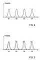
- FIG. 4is a graph illustrating a probability density distribution for the threshold voltage of a system of four charge level flash memory cells
- FIG. 5is a graph illustrating the shift profile for the probability distribution for the threshold voltage of a system of four charge level flash memory cells
- FIG. 6schematically illustrates a high gain coding scheme in accordance with various embodiments of the present invention.
- FIGS. 7 and 8schematically illustrate exemplary channel block implementations in accordance with various embodiments of the present invention.
- the phrase “A/B”means A or B.
- the phrase “A and/or B”means “(A), (B), or (A and B)”.
- the phrase “at least one of A, B, and C”means “(A), (B), (C), (A and B), (A and C), (B and C), or (A, B and C)”.
- the phrase “(A)B”means “(B) or (AB)” that is, A is an optional element.
- Embodiments of the present inventionprovide multi-level signal memory with LDPC and interleaving.
- Memory arrangement 100includes one or more memory blocks 102 that each includes memory cell arrays, as well as read and write circuits.
- Memory arrangement 100also includes a channel block 104 that performs signal processing used to decode signal levels received from memory blocks 102 .
- channel block 104also performs signal processing to code various data values to write into memory blocks 102 .
- a controller 108is provided to interface to external system(s) to receive and send data signals through its external data interface, to and from channel block 104 .
- Controller 106performs various tasks including tasks that direct where data values need to be written into or read from memory blocks 102 depending upon command instructions received through its external interface.
- memory blocks 102may be flash memory blocks.
- a high gain codingsuch as, for example, trellis coded modulation (TCM) is used by channel block 104 to code and/or decode multi-level signal data values to and/or from a memory block.
- TCMtrellis coded modulation
- the addition of TCMimposes a certain constraint as to what sample sets may be adjacent to a previous and a future sample sequence.
- Various codesmay be used to allow multi-level signals data values with a spread distribution that reduces overlaps with one another, enabling the multi-level signals data values to be more likely detected correctly, using e.g. maximum likelihood detection and decoding with trellis coding.
- Pulse Amplitude Modulation code(PAM), Quadrature Amplitude Modulation code (QAM) and Low Density Parity Check code (LDPC) are examples of codes that may be used.
- PAMPulse Amplitude Modulation code
- QAMQuadrature Amplitude Modulation code
- LDPCLow Density Parity Check code
- an exemplary flash memory cellin accordance with various embodiments of the present invention and depicted in FIG. 2 , includes an insulated gate transistor 200 that includes a floating gate 202 between the channel 204 and the control gate 206 .
- Charge trapped in floating gate 202modifies the turn-on threshold voltage.
- the transistor characteristicsare illustrated in FIG. 3 , corresponding to different charge levels stored on floating gate 202 .
- FIG. 4illustrates a typical probability density function (PDF) for the target threshold voltages of a system of flash memory cells, each cell having four target charge levels.
- PDFprobability density function
- FIG. 5illustrates a typical shift profile for the threshold PDF over time.
- the physics of charge leakage in a memory cellis such that each signal level may leak at a different rate from the others. As such, over time, the signal levels generally will not drop at the same rate.
- multi-level signals that are employed to write various data into memory cells within the memory blockare encoded with the high gain coding.
- the high gain encoded data signalsare output to the memory blocks to write data into the memory block cells.
- memory blocks 102 responsive to the commands of controller 108output data that is stored in at least one memory cell.
- data stored in a whole row of memory cellsmay be outputted at different read-back signal levels.
- the multi-level read-back signals for each cellare transferred to channel block 104 . If a small interface is desired, the signals may be transferred in a serial fashion.
- analog to digital conversion or a digitizing functionmay be performed by an analog to digital converter (ADC) that is included on memory block 102 if inclusion of such ADC is practical.
- ADCanalog to digital converter
- analog signalsmay be transferred back to channel block 104 from memory block 102 as discrete time analog signals. Such transfers, in accordance with various embodiments, may be done serially if desired, or in parallel, in other embodiments. In a serial embodiment, the channel block may either digitize the signal or not based upon whether an analog or digital channel implementation is used. In accordance with various embodiments of the present invention a digital channel implementation is used and thus, the channel block includes an ADC, and memory block 102 and channel block 104 are operatively coupled to one another via a digital bus interface.
- a coding scheme in accordance with various embodiments of the present inventionincludes multi-level signal data values being received at channel block 104 from controller 108 .
- the received data valuesare encoded with LDPC via LDPC encoder/de-coder 600 .
- the LDPC coded valuesare then passed through an interleaver 602 .
- the interleaved valuesare mapped to constellation points by the constellation mapper at 604 .
- the systemimplements bit-interleaved coded modulation (BICM).
- BICMbit-interleaved coded modulation
- Gray code mappingis used.
- the constellation mapincludes 8 constellation points.
- the mapped valuesare transferred from channel block 104 to memory block 102 and written into a memory cell of memory block 102 .
- PAMis used to transmit signals between channel block 104 and memory block 102 .
- the channelsmay include ⁇ 7 v, ⁇ 5 v, ⁇ 3 v, ⁇ 1 v, +1 v, +3 v, +5 v and +7 v transmission voltage levels.
- a least significant bite.g. bit 0
- a most significant bite.g. bit 100
- coded multi-level signal data valuesare transferred from the memory block to channel block 104 , where they are decoded.
- the LDPC encoder/de-coder, interleaver and mapperare included with channel block 104 .
- coding schemein accordance with various embodiments of the present invention, more levels may be realized on a multi-level memory device since the coding allows for more reliable retrieval of data values from the memory, even with the reduced distance between levels.
- an exemplary channel block 104may be configured similar to generally known communication or magnetic hard disk drive (HDD) channels, as illustrated in FIG. 7 .
- such an exemplary channel block 104may include an interface 700 , a run length limited (RLL) encoder 702 and channel modulation 704 along a write path.
- RLLrun length limited
- the exemplary channel block 104may further include a variable gain amplifier (VGA) 706 , an offset setting 708 , a continuous time filter (CTF) block 710 , an ADC 712 , a finite impulse response (FIR) block 714 , a Viterbi detector 716 , an RLL decoder 718 , error generators 720 , an offset control loop 722 , a gain control loop 724 , a clock recovery 726 and clock generator 728 along a read path, coupled to each other substantially as illustrated.
- VGAvariable gain amplifier
- CTFcontinuous time filter
- FIRfinite impulse response
- Some simplificationmay be made from a conventional channel block.
- a timing recovery circuit726 , 728 .
- Such a timing recovery circuitmay be included if desired such as, for example, for very high data-rate applications.
- the sampling clock frequencymatches exactly to the incoming data signal frequency and thus, only the delay is potentially unknown. For such a system only a Type I timing recovery loop may be desired.
- the signal returning from memory block 102may match well to the target response, i.e., the original signal, such that linear equalizers in the channel block (CTF 710 and FIR 714 ) may not be necessary.
- Other functional blocks typical of a communication/HDD channelmay be included, in accordance with various embodiments of the present invention, for memory arrangement 100 .
- automatic gain control loop 724 , Viterbi detector 716 (with trellis control) and channel encoder/decoder ( 702 , 718 )may also be included.
- Viterbi detector 716may implement adaptive and non-linear branch metrics calculators (e.g., the Viterbi detector may use a subset non-linear detector algorithm used in magnetic HDD).
- channel block 104may also include a sample data buffer capable of storing a large section of data samples so iterative or over-a-block processing may be performed (e.g., block averaging for gain control so that signal levels may become normalized before other processing by the channel block).
- a sample data buffercapable of storing a large section of data samples so iterative or over-a-block processing may be performed (e.g., block averaging for gain control so that signal levels may become normalized before other processing by the channel block).
- FIG. 8An example of such an arrangement for channel block 104 is schematically illustrated in FIG. 8 .
- such an exemplary channel block 104may include an interface 800 , RLL encoder 802 and channel modulation 804 along a write path.
- the exemplary channel block 104may further include a VGA 806 , offset setting 808 , ADC 810 , sample buffer 812 , offset setting 814 , gain control 816 , offset setting 818 , feed forward offset control 820 , offset setting 822 , gain control 824 , offset setting 826 , offset control 828 , error generator 830 , Viterbi detector 832 and RLL decoder 834 , coupled to each other substantially as illustrated.
- the memory blockis a flash-type memory device.
- the present inventionhas been substantially described as such, although those skilled in the art will understand that other types of memory may benefit from the present invention.
- the present inventionis useful for many types of memory devices such as, for example and not limited to, floating gate devices, oxide-nitride-oxide (ONO) charged trapping devices, and phase change memory devices.
- the portable electronic devicesmay include reduced instruction set (RISC) processors and wireless communication support, such as wireless communication in accordance with one or more of the Institute of Electrical and Electronic Engineer's (IEEE) 802.11 family of standards.
- RISCreduced instruction set
Landscapes
- Engineering & Computer Science (AREA)
- Theoretical Computer Science (AREA)
- Physics & Mathematics (AREA)
- Probability & Statistics with Applications (AREA)
- Quality & Reliability (AREA)
- General Engineering & Computer Science (AREA)
- General Physics & Mathematics (AREA)
- Error Detection And Correction (AREA)
- Techniques For Improving Reliability Of Storages (AREA)
Abstract
Description
Claims (27)
Priority Applications (7)
| Application Number | Priority Date | Filing Date | Title |
|---|---|---|---|
| US11/627,250US7971130B2 (en) | 2006-03-31 | 2007-01-25 | Multi-level signal memory with LDPC and interleaving |
| JP2009502244AJP5356214B2 (en) | 2006-03-31 | 2007-03-27 | Multilevel signal memory with LDPC and interleaving |
| EP07734144AEP2008363A1 (en) | 2006-03-31 | 2007-03-27 | Multi-level memory with ldpc bit interleaved coded modulation |
| KR1020087026874AKR20090005359A (en) | 2006-03-31 | 2007-03-27 | LDPC bit interleaved coded modulation multi-level memory |
| PCT/IB2007/000822WO2007116275A1 (en) | 2006-03-31 | 2007-03-27 | Multi-level memory with ldpc bit interleaved coded modulation |
| IL194484AIL194484A (en) | 2006-03-31 | 2008-10-02 | Multi-level memory with ldpc bit interleaved coded modulation |
| US13/169,790US8869014B2 (en) | 2006-03-31 | 2011-06-27 | Multi-level signal memory with LDPC and interleaving |
Applications Claiming Priority (2)
| Application Number | Priority Date | Filing Date | Title |
|---|---|---|---|
| US78829106P | 2006-03-31 | 2006-03-31 | |
| US11/627,250US7971130B2 (en) | 2006-03-31 | 2007-01-25 | Multi-level signal memory with LDPC and interleaving |
Related Child Applications (1)
| Application Number | Title | Priority Date | Filing Date |
|---|---|---|---|
| US13/169,790ContinuationUS8869014B2 (en) | 2006-03-31 | 2011-06-27 | Multi-level signal memory with LDPC and interleaving |
Publications (2)
| Publication Number | Publication Date |
|---|---|
| US20070245214A1 US20070245214A1 (en) | 2007-10-18 |
| US7971130B2true US7971130B2 (en) | 2011-06-28 |
Family
ID=38328116
Family Applications (2)
| Application Number | Title | Priority Date | Filing Date |
|---|---|---|---|
| US11/627,250Active2030-03-31US7971130B2 (en) | 2006-03-31 | 2007-01-25 | Multi-level signal memory with LDPC and interleaving |
| US13/169,790Active2028-07-17US8869014B2 (en) | 2006-03-31 | 2011-06-27 | Multi-level signal memory with LDPC and interleaving |
Family Applications After (1)
| Application Number | Title | Priority Date | Filing Date |
|---|---|---|---|
| US13/169,790Active2028-07-17US8869014B2 (en) | 2006-03-31 | 2011-06-27 | Multi-level signal memory with LDPC and interleaving |
Country Status (6)
| Country | Link |
|---|---|
| US (2) | US7971130B2 (en) |
| EP (1) | EP2008363A1 (en) |
| JP (1) | JP5356214B2 (en) |
| KR (1) | KR20090005359A (en) |
| IL (1) | IL194484A (en) |
| WO (1) | WO2007116275A1 (en) |
Cited By (16)
| Publication number | Priority date | Publication date | Assignee | Title |
|---|---|---|---|---|
| US20120102379A1 (en)* | 2010-10-22 | 2012-04-26 | Sandisk Corporation | System and method of interleaving data according to an adjustable parameter |
| US8219886B1 (en)* | 2006-01-20 | 2012-07-10 | Marvell International Ltd. | High density multi-level memory |
| US8527849B2 (en)* | 2011-08-19 | 2013-09-03 | Stec, Inc. | High speed hard LDPC decoder |
| US20130326306A1 (en)* | 2012-05-29 | 2013-12-05 | International Business Machines Corporation | Partial reverse concatenation for data storage devices using composite codes |
| US8792274B1 (en) | 2007-10-01 | 2014-07-29 | Marvell International Ltd. | Multi-level memory cell read, program, and erase techniques |
| US20140215285A1 (en)* | 2013-01-31 | 2014-07-31 | Lsi Corporation | Integrated-interleaved low density parity check (ldpc) codes |
| US20150039973A1 (en)* | 2013-07-05 | 2015-02-05 | Samsung Electronics Co., Ltd. | Transmitter apparatus and signal processing method thereof |
| US20150236721A1 (en)* | 2014-02-19 | 2015-08-20 | Samsung Electronics Co., Ltd. | Transmitting apparatus and interleaving method thereof |
| US9178534B2 (en) | 2012-05-29 | 2015-11-03 | International Business Machines Corporation | Methods for partial reverse concatenation for data storage devices using composite codes |
| US9183852B2 (en) | 2012-05-29 | 2015-11-10 | International Business Machines Corporation | Magnetic tape recording in data format using an efficient reverse concatenated modulation code |
| US9595978B2 (en)* | 2015-05-19 | 2017-03-14 | Samsung Electronics Co., Ltd. | Transmitting apparatus and interleaving method thereof |
| US9634692B2 (en)* | 2015-05-19 | 2017-04-25 | Samsung Electronics Co., Ltd. | Transmitting apparatus and interleaving method thereof |
| US9680505B2 (en)* | 2015-05-19 | 2017-06-13 | Samsung Electronics Co., Ltd. | Transmitting apparatus and interleaving method thereof |
| US9692453B2 (en)* | 2015-05-19 | 2017-06-27 | Samsung Electronics Co., Ltd. | Transmitting apparatus and interleaving method thereof |
| US11082159B2 (en) | 2013-07-05 | 2021-08-03 | Samsung Electronics Co., Ltd. | Transmitter apparatus and signal processing method thereof |
| US11563448B2 (en) | 2014-02-19 | 2023-01-24 | Samsung Electronics Co., Ltd. | Receiving apparatus and de-interleaving method thereof |
Families Citing this family (37)
| Publication number | Priority date | Publication date | Assignee | Title |
|---|---|---|---|---|
| US8725929B1 (en) | 2006-11-06 | 2014-05-13 | Marvell World Trade Ltd. | Adaptive read and write systems and methods for memory cells |
| US8645793B2 (en) | 2008-06-03 | 2014-02-04 | Marvell International Ltd. | Statistical tracking for flash memory |
| US7941590B2 (en)* | 2006-11-06 | 2011-05-10 | Marvell World Trade Ltd. | Adaptive read and write systems and methods for memory cells |
| US7992070B2 (en)* | 2006-12-27 | 2011-08-02 | Nec Laboratories America, Inc. | Bit-interleaved LDPC-coded modulation for high-speed optical transmission |
| US7808834B1 (en) | 2007-04-13 | 2010-10-05 | Marvell International Ltd. | Incremental memory refresh |
| US8031526B1 (en) | 2007-08-23 | 2011-10-04 | Marvell International Ltd. | Write pre-compensation for nonvolatile memory |
| US8189381B1 (en) | 2007-08-28 | 2012-05-29 | Marvell International Ltd. | System and method for reading flash memory cells |
| US8085605B2 (en) | 2007-08-29 | 2011-12-27 | Marvell World Trade Ltd. | Sequence detection for flash memory with inter-cell interference |
| TWI538415B (en) | 2007-11-26 | 2016-06-11 | Sony Corp | Data processing device and data processing method |
| TWI390856B (en) | 2007-11-26 | 2013-03-21 | Sony Corp | Data processing device and data processing method |
| EP2308058B1 (en)* | 2008-07-01 | 2016-01-27 | LSI Corporation | Methods and apparatus for read-side intercell interference mitigation in flash memories |
| US8301979B2 (en)* | 2008-10-07 | 2012-10-30 | Sandisk Il Ltd. | Low density parity code (LDPC) decoding for memory with multiple log likelihood ratio (LLR) decoders |
| US8583979B1 (en)* | 2008-10-17 | 2013-11-12 | Sk Hynix Memory Solutions Inc. | Multiple interleavers in a coding system |
| US20100220514A1 (en)* | 2009-03-02 | 2010-09-02 | Lyric Semiconductor, Inc. | Storage devices with soft processing |
| US8458114B2 (en)* | 2009-03-02 | 2013-06-04 | Analog Devices, Inc. | Analog computation using numerical representations with uncertainty |
| US8107306B2 (en) | 2009-03-27 | 2012-01-31 | Analog Devices, Inc. | Storage devices with soft processing |
| KR101678407B1 (en)* | 2010-05-10 | 2016-11-23 | 삼성전자주식회사 | Data storage device and program method thereof |
| US8464137B2 (en) | 2010-12-03 | 2013-06-11 | International Business Machines Corporation | Probabilistic multi-tier error correction in not-and (NAND) flash memory |
| EP2525496A1 (en)* | 2011-05-18 | 2012-11-21 | Panasonic Corporation | Bit-interleaved coding and modulation (BICM) with quasi-cyclic LDPC codes |
| WO2013065085A1 (en) | 2011-11-01 | 2013-05-10 | Hitachi, Ltd. | Nonvolatile storage system compensating prior probability for low-density parity check codes |
| US8892986B2 (en)* | 2012-03-08 | 2014-11-18 | Micron Technology, Inc. | Apparatuses and methods for combining error coding and modulation schemes |
| US9098105B2 (en)* | 2012-08-24 | 2015-08-04 | Avago Technologies General Ip (Singapore) Pte. Ltd. | Dynamic Y-buffer size adjustment for retained sector reprocessing |
| US9059737B2 (en) | 2013-01-11 | 2015-06-16 | HGST Netherlands B.V. | Disk drive with distributed codeword blocks |
| US9196299B2 (en)* | 2013-08-23 | 2015-11-24 | Avago Technologies General Ip (Singapore) Pte. Ltd. | Systems and methods for enhanced data encoding and decoding |
| US9602141B2 (en) | 2014-04-21 | 2017-03-21 | Sandisk Technologies Llc | High-speed multi-block-row layered decoder for low density parity check (LDPC) codes |
| US9748973B2 (en)* | 2014-04-22 | 2017-08-29 | Sandisk Technologies Llc | Interleaved layered decoder for low-density parity check codes |
| US9503125B2 (en) | 2014-05-08 | 2016-11-22 | Sandisk Technologies Llc | Modified trellis-based min-max decoder for non-binary low-density parity-check error-correcting codes |
| KR102287625B1 (en)* | 2015-02-16 | 2021-08-10 | 한국전자통신연구원 | Bit interleaver for 4096-symbol mapping and low density parity check codeword with 64800 length, 2/15 rate, and method using the same |
| KR102287627B1 (en)* | 2015-02-16 | 2021-08-10 | 한국전자통신연구원 | Bit interleaver for 4096-symbol mapping and low density parity check codeword with 64800 length, 4/15 rate, and method using the same |
| KR102287623B1 (en)* | 2015-02-16 | 2021-08-10 | 한국전자통신연구원 | Bit interleaver for 1024-symbol mapping and low density parity check codeword with 64800 length, 4/15 rate, and method using the same |
| US10425260B2 (en) | 2017-08-07 | 2019-09-24 | Micron Technology, Inc. | Multi-level signaling in memory with wide system interface |
| US10277435B2 (en) | 2017-08-07 | 2019-04-30 | Micron Technology, Inc. | Method to vertically align multi-level cells |
| US10447512B2 (en)* | 2017-08-07 | 2019-10-15 | Micron Technology, Inc. | Channel equalization for multi-level signaling |
| US10530617B2 (en) | 2017-08-07 | 2020-01-07 | Micron Technology, Inc. | Programmable channel equalization for multi-level signaling |
| US11437112B2 (en) | 2018-12-06 | 2022-09-06 | Micron Technology, Inc. | Multi-level signaling for a memory device |
| US11870616B2 (en)* | 2020-01-27 | 2024-01-09 | Micron Technology, Inc. | Postamble for multi-level signal modulation |
| US11481271B2 (en)* | 2021-03-16 | 2022-10-25 | Western Digital Technologies, Inc. | Storage system and method for using subcodes and convolutional-based LDPC interleaved coding schemes with read threshold calibration support |
Citations (4)
| Publication number | Priority date | Publication date | Assignee | Title |
|---|---|---|---|---|
| US6125050A (en)* | 1996-12-17 | 2000-09-26 | Siemens Aktiengesellschaft | Configuration for driving parallel lines in a memory cell configuration |
| US7373581B2 (en)* | 2002-12-03 | 2008-05-13 | Nec Corporation | Device, program, and method for decoding LDPC codes |
| US7421041B2 (en)* | 2004-03-01 | 2008-09-02 | Qualcomm, Incorporated | Iterative channel and interference estimation and decoding |
| US7516390B2 (en)* | 2005-01-10 | 2009-04-07 | Broadcom Corporation | LDPC (Low Density Parity Check) coding and interleaving implemented in MIMO communication systems |
Family Cites Families (10)
| Publication number | Priority date | Publication date | Assignee | Title |
|---|---|---|---|---|
| US7043681B2 (en) | 2002-05-03 | 2006-05-09 | Ibiquity Digital Corporation | Digital audio broadcasting method and apparatus using complementary pattern-mapped convolutional codes |
| US7231557B2 (en)* | 2003-04-02 | 2007-06-12 | Qualcomm Incorporated | Methods and apparatus for interleaving in a block-coherent communication system |
| JP2005078721A (en) | 2003-09-01 | 2005-03-24 | Nippon Telegr & Teleph Corp <Ntt> | Error correction method and memory circuit |
| US7334181B2 (en)* | 2003-09-04 | 2008-02-19 | The Directv Group, Inc. | Method and system for providing short block length low density parity check (LDPC) codes |
| US7281192B2 (en)* | 2004-04-05 | 2007-10-09 | Broadcom Corporation | LDPC (Low Density Parity Check) coded signal decoding using parallel and simultaneous bit node and check node processing |
| US7243287B2 (en)* | 2004-05-03 | 2007-07-10 | Broadcom Corporation | Decoding LDPC (Low Density Parity Check) code and graphs using multiplication (or addition in log-domain) on both sides of bipartite graph |
| US7760880B2 (en)* | 2004-10-13 | 2010-07-20 | Viasat, Inc. | Decoder architecture system and method |
| US8122315B2 (en)* | 2005-12-01 | 2012-02-21 | Electronics And Telecommunications Research Institute | LDPC decoding apparatus and method using type-classified index |
| US8006172B2 (en)* | 2007-07-10 | 2011-08-23 | Oracle America, Inc. | Auxiliary path iterative decoding |
| US8020063B2 (en)* | 2007-07-26 | 2011-09-13 | Harris Corporation | High rate, long block length, low density parity check encoder |
- 2007
- 2007-01-25USUS11/627,250patent/US7971130B2/enactiveActive
- 2007-03-27KRKR1020087026874Apatent/KR20090005359A/ennot_activeCeased
- 2007-03-27WOPCT/IB2007/000822patent/WO2007116275A1/enactiveApplication Filing
- 2007-03-27JPJP2009502244Apatent/JP5356214B2/enactiveActive
- 2007-03-27EPEP07734144Apatent/EP2008363A1/ennot_activeCeased
- 2008
- 2008-10-02ILIL194484Apatent/IL194484A/enactiveIP Right Grant
- 2011
- 2011-06-27USUS13/169,790patent/US8869014B2/enactiveActive
Patent Citations (4)
| Publication number | Priority date | Publication date | Assignee | Title |
|---|---|---|---|---|
| US6125050A (en)* | 1996-12-17 | 2000-09-26 | Siemens Aktiengesellschaft | Configuration for driving parallel lines in a memory cell configuration |
| US7373581B2 (en)* | 2002-12-03 | 2008-05-13 | Nec Corporation | Device, program, and method for decoding LDPC codes |
| US7421041B2 (en)* | 2004-03-01 | 2008-09-02 | Qualcomm, Incorporated | Iterative channel and interference estimation and decoding |
| US7516390B2 (en)* | 2005-01-10 | 2009-04-07 | Broadcom Corporation | LDPC (Low Density Parity Check) coding and interleaving implemented in MIMO communication systems |
Non-Patent Citations (18)
| Title |
|---|
| 802.11h, IEEE Standard for Information technology-Telectommunications and information exchange between systems-Local and metropolitan area networks-Specific requirements, Part 11: Wireless LAN Medium Access Control (MAC) and Physical Layer (PHY) specifications, Amendment 6: Medium Access Control (MAC) Security Enhancements, IEEE Std 802.11i-2004, 190 pgs. |
| 802.11h, IEEE Standard for Information technology-Telectommunications and information exchange between systems-Local and metropolitan area networks-Specific requirements-Part 11: Wireless LAN Medium Access Control (MAC) and Physical Layer (PHY) specifications, Amendment 5: Spectrum and Transmit Power Management Extensions in the 5 GHz band in Europe, IEEE Std 802.11h-2003, 75 pgs. |
| Draft Supplement to Standard [for] Information Technology-Telecommunications and information exchange between systems-Local and metropolitan area networks-Specific requirements-Part 11: Wireless LAN Medium Access Control (MAC) and Physical Layer (PHY) specifications: Further Higher-Speed Physical Layer Extension in the 2.4 GHz Band, IEEE Std 802.11g/D2.8, May 2002, 53 pgs. |
| Draft Supplement to Standard for Information Technology-Telecommunications and Information Exchange Between Systems-LAN/MAN Specific Requirements-Part 11: Wireless LAN Medium Access Control (MAC) and Physical Layer (PHY) specifications: Specification for Enhanced Security, IEEE STD 802.11i/D3.0, Nov. 2002, 211 pgs. |
| Gregori S et al: "Construction of polyvalent error control codes for multilevel memories", Proc. Intern. Conference on Electronics, Circuits and Systems, vol. 2, Dec. 17, 2000, pp. 751-754, XP010535817. |
| Hsi-Chia Chang et al: "Multi-level memory systems using error control codes", Proceedings of the 2004 International Symposium on Circuits and Systems, vol. 2, May 23, 2004, pp. 393-396, XP010720188. |
| IEEE P802.11, Wireless LANs, TGn Sync Proposal Technical Specification, May 18, 2005, IEEE 802.11-04/08898r6, 131 pgs. |
| IEEE P802.11g/D8.2, Draft Supplement to Standard [for] Information Technology-Telecommunications and information exchange between systems-Local and metropolitan area networks-Specific requirements-Part 11: Wireless LAN Medium Access Control (MAC) and Physical Layer (PHY) specification: Further Higher Data Rate Extension in the 2.4 GHz Band, Apr. 2003, 69 pgs. |
| IEEE P802.11g/D8.2, Draft Supplement to Standard [for] Information Technology-Telecommunications and information exchange between systems-Local and metropolitan area networks-Specific requirements-Part 11: Wireless LAN Medium Access Control (MAC) and Physical Layer (PHY) specifications: Further Higher Data Rate Extension in the 2.4 GHz Band, Apr. 2003, 69 pgs. |
| IEEE Standard for Information technology-Telectommunications and information exchange between systems-Local and metropolitan area networks-Specific requirements-Part 11: Wireless LAN Medium Access Control (MAC) and Physical Layer (PHY) specifications: Amendment 2: Higher-Speed Physical Layer (PHY) extension in the 2.4 [continued on p. 2] HGz Band-Corrigendum 1, IEEE Std 802.11b-1999/Cor Jan. 2001, 23 pgs. |
| IEEE Standard for Information technology-Telectommunications and information exchange between systems-Local and metropolitan area networks-Specific requirements-Part 11: Wireless LAN Medium Access Control (MAC) and Physical Layer (PHY) specifications: Amendment 7: Medium Access Control (MAC) Quality of Service (QoS) Enhancements, IEEE 802.11e/D11.0, Oct. 2004, 195 pgs. |
| International Standard, Information technology-Telectommunications and information exchange between systems-Local and metropolitan area networks-Specific requirements-Part 11: Wireless LAN Medium Access Control (MAC) and Physical Layer (PHY) specifications, ISO/IEC 8802-11:1999(E), ANSI/IEEE, Std 802.11, 1999 edition, 531 pages. |
| Lou H-L et al: "Coded Modulation to Increase Storage Capacity of Multilevel Memories", Proc. IEEE Globecom 1998, vol. vol 6, 1998, pp. 3379-3384, XP000805261. |
| Rossi D et al: "Fast and compact error correcting scheme for reliable multilevel flash memories", Proceedings of the Eighth IEEE International On-Line Testing Workshop, Jul. 8, 2002, pp. 221-225, XP010601444. |
| Supplemental to IEEE Standard for Information technology-Telecommunications and information exchange between systems-Local and metropolitan area networks-Specific requirements-Part 11: Wireless LAN Medium Access Control (MAC) and Physical Layer (PHY) specifications: Higher-Speed Physical Layer Extension in the 2.4 HGz Band, IEEE Std 802.11b-1999, 96 pgs. |
| Supplemental to IEEE Standard for Information technology-Telecommunications and information exchange between systems-Local and metropolitan area networks-Specific requirements-Part 11: Wireless LAN Medium Access Control (MAC) and Physical Layer (PHY) specifications: High-speed Physical Layer in the 5 GHZ Band, IEEE Std 802.11a-1999, 91 pgs. |
| Winstead C: "Analog Soft Decoding for Multi-Level Memories", Proceedings 35th International Symposium on Multiple-Valued Logic, May 19, 2005, pp. 132-137, XP010798331. |
| Zhang Zhi et al: "Low-density parity-check codes and high spectral efficiency modulation", Proc. Personal, Indoor and Mobile Radio Communications Conference, Sep. 7, 2003, pp. 444-448, XP010681635. |
Cited By (38)
| Publication number | Priority date | Publication date | Assignee | Title |
|---|---|---|---|---|
| US8583991B1 (en) | 2006-01-20 | 2013-11-12 | Marvell International Ltd. | High density multi-level memory |
| US8219886B1 (en)* | 2006-01-20 | 2012-07-10 | Marvell International Ltd. | High density multi-level memory |
| US8792274B1 (en) | 2007-10-01 | 2014-07-29 | Marvell International Ltd. | Multi-level memory cell read, program, and erase techniques |
| US8560919B2 (en)* | 2010-10-22 | 2013-10-15 | Sandisk Technologies Inc. | System and method of interleaving data according to an adjustable parameter |
| US20120102379A1 (en)* | 2010-10-22 | 2012-04-26 | Sandisk Corporation | System and method of interleaving data according to an adjustable parameter |
| US8527849B2 (en)* | 2011-08-19 | 2013-09-03 | Stec, Inc. | High speed hard LDPC decoder |
| US9190076B2 (en) | 2012-05-29 | 2015-11-17 | International Business Machines Corporation | Data format using an efficient reverse concatenated modulation code for magnetic tape recording |
| US20130326306A1 (en)* | 2012-05-29 | 2013-12-05 | International Business Machines Corporation | Partial reverse concatenation for data storage devices using composite codes |
| US11381258B2 (en) | 2012-05-29 | 2022-07-05 | Awemane Ltd. | Partial reverse concatenation for data storage devices using composite codes |
| US10680655B2 (en) | 2012-05-29 | 2020-06-09 | International Business Machines Corporation | Partial reverse concatenation for data storage devices using composite codes |
| US10484018B2 (en) | 2012-05-29 | 2019-11-19 | International Business Machines Corporation | Partial reverse concatenation for data storage devices using composite codes |
| US9558782B2 (en)* | 2012-05-29 | 2017-01-31 | International Business Machines Corporation | Partial reverse concatenation for data storage devices using composite codes |
| US9178534B2 (en) | 2012-05-29 | 2015-11-03 | International Business Machines Corporation | Methods for partial reverse concatenation for data storage devices using composite codes |
| US9183852B2 (en) | 2012-05-29 | 2015-11-10 | International Business Machines Corporation | Magnetic tape recording in data format using an efficient reverse concatenated modulation code |
| US9077378B2 (en)* | 2013-01-31 | 2015-07-07 | Lsi Corporation | Integrated-interleaved low density parity check (LDPC) codes |
| US9160367B2 (en) | 2013-01-31 | 2015-10-13 | Seagate Technology Llc | Integrated-interleaved low density parity check (LDPC) codes |
| US20140215285A1 (en)* | 2013-01-31 | 2014-07-31 | Lsi Corporation | Integrated-interleaved low density parity check (ldpc) codes |
| US10367606B2 (en) | 2013-07-05 | 2019-07-30 | Samsung Electronics Co., Ltd. | Transmitter apparatus and signal processing method thereof |
| US11936478B2 (en) | 2013-07-05 | 2024-03-19 | Samsung Electronics Co., Ltd. | Transmitter apparatus and signal processing method thereof |
| US11601220B2 (en) | 2013-07-05 | 2023-03-07 | Samsung Electronics Co., Ltd. | Transmitter apparatus and signal processing method thereof |
| US11082159B2 (en) | 2013-07-05 | 2021-08-03 | Samsung Electronics Co., Ltd. | Transmitter apparatus and signal processing method thereof |
| US20150039973A1 (en)* | 2013-07-05 | 2015-02-05 | Samsung Electronics Co., Ltd. | Transmitter apparatus and signal processing method thereof |
| US9484957B2 (en)* | 2013-07-05 | 2016-11-01 | Samsung Electronics Co., Ltd. | Transmitter apparatus and signal processing method thereof |
| US9602137B2 (en)* | 2014-02-19 | 2017-03-21 | Samsung Electronics Co., Ltd. | Transmitting apparatus and interleaving method thereof |
| US11563448B2 (en) | 2014-02-19 | 2023-01-24 | Samsung Electronics Co., Ltd. | Receiving apparatus and de-interleaving method thereof |
| US20150236721A1 (en)* | 2014-02-19 | 2015-08-20 | Samsung Electronics Co., Ltd. | Transmitting apparatus and interleaving method thereof |
| US10367531B2 (en) | 2015-05-19 | 2019-07-30 | Samsung Electronics Co., Ltd. | Transmitting apparatus and interleaving method thereof |
| US10367532B2 (en) | 2015-05-19 | 2019-07-30 | Samsung Electronics Co., Ltd. | Transmitting apparatus and interleaving method thereof |
| US10361725B2 (en) | 2015-05-19 | 2019-07-23 | Samsung Electronics Co., Ltd. | Transmitting apparatus and interleaving method thereof |
| US11057050B2 (en) | 2015-05-19 | 2021-07-06 | Samsung Electronics Co., Ltd. | Transmitting apparatus and interleaving method thereof |
| US11057056B2 (en) | 2015-05-19 | 2021-07-06 | Samsung Electronics Co., Ltd. | Transmitting apparatus and interleaving method thereof |
| US11057057B2 (en) | 2015-05-19 | 2021-07-06 | Samsung Electronics Co., Ltd. | Transmitting apparatus and interleaving method thereof |
| US10348330B2 (en) | 2015-05-19 | 2019-07-09 | Samsung Electronics Co., Ltd. | Transmitting apparatus and interleaving method thereof |
| US11133830B2 (en) | 2015-05-19 | 2021-09-28 | Samsung Electronics Co., Ltd. | Transmitting apparatus and interleaving method thereof |
| US9692453B2 (en)* | 2015-05-19 | 2017-06-27 | Samsung Electronics Co., Ltd. | Transmitting apparatus and interleaving method thereof |
| US9680505B2 (en)* | 2015-05-19 | 2017-06-13 | Samsung Electronics Co., Ltd. | Transmitting apparatus and interleaving method thereof |
| US9634692B2 (en)* | 2015-05-19 | 2017-04-25 | Samsung Electronics Co., Ltd. | Transmitting apparatus and interleaving method thereof |
| US9595978B2 (en)* | 2015-05-19 | 2017-03-14 | Samsung Electronics Co., Ltd. | Transmitting apparatus and interleaving method thereof |
Also Published As
| Publication number | Publication date |
|---|---|
| JP2009531767A (en) | 2009-09-03 |
| KR20090005359A (en) | 2009-01-13 |
| EP2008363A1 (en) | 2008-12-31 |
| US20070245214A1 (en) | 2007-10-18 |
| IL194484A0 (en) | 2009-08-03 |
| US20110258509A1 (en) | 2011-10-20 |
| US8869014B2 (en) | 2014-10-21 |
| JP5356214B2 (en) | 2013-12-04 |
| IL194484A (en) | 2012-10-31 |
| WO2007116275A1 (en) | 2007-10-18 |
Similar Documents
| Publication | Publication Date | Title |
|---|---|---|
| US7971130B2 (en) | Multi-level signal memory with LDPC and interleaving | |
| US8583991B1 (en) | High density multi-level memory | |
| TWI459402B (en) | Memory system, method for reading data stored in a memory cell of a memory | |
| EP1987519B1 (en) | Method and system for error correction in flash memory | |
| KR101373789B1 (en) | Flash memory with coding and signal processing | |
| US8156398B2 (en) | Parameter estimation based on error correction code parity check equations | |
| US8156403B2 (en) | Combined distortion estimation and error correction coding for memory devices | |
| CN101512661B (en) | Combined distortion estimation and error correction coding for memory devices | |
| US8266484B1 (en) | Circuits, architectures, apparatuses, systems, methods, algorithms, software and firmware for using reserved cells to indicate defect positions | |
| US9582359B2 (en) | Write mapping to mitigate hard errors via soft-decision decoding | |
| JP4999921B2 (en) | Combination of distortion estimation and error correction coding for memory devices. | |
| CN101868829A (en) | M + N bit programming and M + L bit read for M bit memory cells | |
| CN111190764A (en) | Method for obtaining soft information of LDPC code of NAND flash memory |
Legal Events
| Date | Code | Title | Description |
|---|---|---|---|
| AS | Assignment | Owner name:MARVELL SEMICONDUCTOR, INC., CALIFORNIA Free format text:ASSIGNMENT OF ASSIGNORS INTEREST;ASSIGNOR:RAMAMOORTHY, ADITYA;REEL/FRAME:018805/0950 Effective date:20070124 | |
| AS | Assignment | Owner name:MARVELL WORLD TRADE LTD., BARBADOS Free format text:ASSIGNMENT OF ASSIGNORS INTEREST;ASSIGNOR:MARVELL INTERNATIONAL LTD.;REEL/FRAME:019020/0694 Effective date:20070308 Owner name:MARVELL INTERNATIONAL LTD., BERMUDA Free format text:ASSIGNMENT OF ASSIGNORS INTEREST;ASSIGNOR:MARVELL SEMICONDUCTOR, INC.;REEL/FRAME:019020/0666 Effective date:20070307 Owner name:MARVELL INTERNATIONAL LTD., BERMUDA Free format text:LICENSE;ASSIGNOR:MARVELL WORLD TRADE LTD.;REEL/FRAME:019020/0741 Effective date:20070312 | |
| STCF | Information on status: patent grant | Free format text:PATENTED CASE | |
| FPAY | Fee payment | Year of fee payment:4 | |
| MAFP | Maintenance fee payment | Free format text:PAYMENT OF MAINTENANCE FEE, 8TH YEAR, LARGE ENTITY (ORIGINAL EVENT CODE: M1552); ENTITY STATUS OF PATENT OWNER: LARGE ENTITY Year of fee payment:8 | |
| AS | Assignment | Owner name:MARVELL INTERNATIONAL LTD., BERMUDA Free format text:ASSIGNMENT OF ASSIGNORS INTEREST;ASSIGNOR:MARVELL WORLD TRADE LTD.;REEL/FRAME:051778/0537 Effective date:20191231 | |
| AS | Assignment | Owner name:CAVIUM INTERNATIONAL, CAYMAN ISLANDS Free format text:ASSIGNMENT OF ASSIGNORS INTEREST;ASSIGNOR:MARVELL INTERNATIONAL LTD.;REEL/FRAME:052918/0001 Effective date:20191231 | |
| AS | Assignment | Owner name:MARVELL ASIA PTE, LTD., SINGAPORE Free format text:ASSIGNMENT OF ASSIGNORS INTEREST;ASSIGNOR:CAVIUM INTERNATIONAL;REEL/FRAME:053475/0001 Effective date:20191231 | |
| MAFP | Maintenance fee payment | Free format text:PAYMENT OF MAINTENANCE FEE, 12TH YEAR, LARGE ENTITY (ORIGINAL EVENT CODE: M1553); ENTITY STATUS OF PATENT OWNER: LARGE ENTITY Year of fee payment:12 |