US7970987B2 - Partial block data programming and reading operations in a non-volatile memory - Google Patents
Partial block data programming and reading operations in a non-volatile memoryDownload PDFInfo
- Publication number
- US7970987B2 US7970987B2US12/900,397US90039710AUS7970987B2US 7970987 B2US7970987 B2US 7970987B2US 90039710 AUS90039710 AUS 90039710AUS 7970987 B2US7970987 B2US 7970987B2
- Authority
- US
- United States
- Prior art keywords
- data
- page
- pages
- block
- new
- Prior art date
- Legal status (The legal status is an assumption and is not a legal conclusion. Google has not performed a legal analysis and makes no representation as to the accuracy of the status listed.)
- Expired - Fee Related
Links
Images


Classifications
- G—PHYSICS
- G11—INFORMATION STORAGE
- G11C—STATIC STORES
- G11C16/00—Erasable programmable read-only memories
- G11C16/02—Erasable programmable read-only memories electrically programmable
- G11C16/06—Auxiliary circuits, e.g. for writing into memory
- G11C16/10—Programming or data input circuits
- G11C16/102—External programming circuits, e.g. EPROM programmers; In-circuit programming or reprogramming; EPROM emulators
- G—PHYSICS
- G06—COMPUTING OR CALCULATING; COUNTING
- G06F—ELECTRIC DIGITAL DATA PROCESSING
- G06F12/00—Accessing, addressing or allocating within memory systems or architectures
- G06F12/02—Addressing or allocation; Relocation
- G—PHYSICS
- G06—COMPUTING OR CALCULATING; COUNTING
- G06F—ELECTRIC DIGITAL DATA PROCESSING
- G06F12/00—Accessing, addressing or allocating within memory systems or architectures
- G06F12/02—Addressing or allocation; Relocation
- G06F12/0223—User address space allocation, e.g. contiguous or non contiguous base addressing
- G06F12/023—Free address space management
- G06F12/0238—Memory management in non-volatile memory, e.g. resistive RAM or ferroelectric memory
- G06F12/0246—Memory management in non-volatile memory, e.g. resistive RAM or ferroelectric memory in block erasable memory, e.g. flash memory
- G—PHYSICS
- G11—INFORMATION STORAGE
- G11C—STATIC STORES
- G11C16/00—Erasable programmable read-only memories
- G11C16/02—Erasable programmable read-only memories electrically programmable
- G11C16/06—Auxiliary circuits, e.g. for writing into memory
- G11C16/10—Programming or data input circuits
- G11C16/102—External programming circuits, e.g. EPROM programmers; In-circuit programming or reprogramming; EPROM emulators
- G11C16/105—Circuits or methods for updating contents of nonvolatile memory, especially with 'security' features to ensure reliable replacement, i.e. preventing that old data is lost before new data is reliably written
- G—PHYSICS
- G06—COMPUTING OR CALCULATING; COUNTING
- G06F—ELECTRIC DIGITAL DATA PROCESSING
- G06F2212/00—Indexing scheme relating to accessing, addressing or allocation within memory systems or architectures
- G06F2212/10—Providing a specific technical effect
- G06F2212/1016—Performance improvement
- G—PHYSICS
- G06—COMPUTING OR CALCULATING; COUNTING
- G06F—ELECTRIC DIGITAL DATA PROCESSING
- G06F2212/00—Indexing scheme relating to accessing, addressing or allocation within memory systems or architectures
- G06F2212/10—Providing a specific technical effect
- G06F2212/1032—Reliability improvement, data loss prevention, degraded operation etc
- G—PHYSICS
- G06—COMPUTING OR CALCULATING; COUNTING
- G06F—ELECTRIC DIGITAL DATA PROCESSING
- G06F2212/00—Indexing scheme relating to accessing, addressing or allocation within memory systems or architectures
- G06F2212/72—Details relating to flash memory management
- G06F2212/7202—Allocation control and policies
- G—PHYSICS
- G06—COMPUTING OR CALCULATING; COUNTING
- G06F—ELECTRIC DIGITAL DATA PROCESSING
- G06F2212/00—Indexing scheme relating to accessing, addressing or allocation within memory systems or architectures
- G06F2212/72—Details relating to flash memory management
- G06F2212/7208—Multiple device management, e.g. distributing data over multiple flash devices
- G—PHYSICS
- G06—COMPUTING OR CALCULATING; COUNTING
- G06F—ELECTRIC DIGITAL DATA PROCESSING
- G06F2212/00—Indexing scheme relating to accessing, addressing or allocation within memory systems or architectures
- G06F2212/72—Details relating to flash memory management
- G06F2212/7209—Validity control, e.g. using flags, time stamps or sequence numbers
- G—PHYSICS
- G11—INFORMATION STORAGE
- G11C—STATIC STORES
- G11C2216/00—Indexing scheme relating to G11C16/00 and subgroups, for features not directly covered by these groups
- G11C2216/12—Reading and writing aspects of erasable programmable read-only memories
- G11C2216/16—Flash programming of all the cells in an array, sector or block simultaneously
Definitions
- This inventionpertains to the field of semiconductor non-volatile data storage system architectures and their methods of operation, and has application to data storage systems based on flash electrically erasable and programmable read-only memories (EEPROMs).
- EEPROMselectrically erasable and programmable read-only memories
- flash EEPROM devicesA common application of flash EEPROM devices is as a mass data storage subsystem for electronic devices. Such subsystems are commonly implemented as either removable memory cards that can be inserted into multiple host systems or as non-removable embedded storage within the host system. In both implementations, the subsystem includes one or more flash devices and often a subsystem controller.
- Flash EEPROM devicesare composed of one or more arrays of transistor cells, each cell capable of non-volatile storage of one or more bits of data. Thus flash memory does not require power to retain the data programmed therein. Once programmed however, a cell must be erased before it can be reprogrammed with a new data value.
- These arrays of cellsare partitioned into groups to provide for efficient implementation of read, program and erase functions.
- a typical flash memory architecture for mass storagearranges large groups of cells into erasable blocks, wherein a block contains the smallest number of cells (unit of erase) that are erasable at one time.
- each blockcontains enough cells to store one sector of user data plus some overhead data related to the user data and/or to the block in which it is stored.
- the amount of user data included in a sectoris the standard 512 bytes in one class of such memory systems but can be of some other size. Because the isolation of individual blocks of cells from one another that is required to make them individually erasable takes space on the integrated circuit chip, another class of flash memories makes the blocks significantly larger so there is less space required for such isolation. But since it is also desired to handle user data in much smaller sectors, each large block is often further partitioned into individually addressable pages that are the basic unit for reading and programming user data (unit of programming and/or reading). Each page usually stores one sector of user data, but a page may store a partial sector or multiple sectors.
- a “sector”is used herein to refer to an amount of user data that is transferred to and from the host as a unit.
- the subsystem controller in a large block systemperforms a number of functions including the translation between logical addresses (LBAs) received by the memory sub-system from a host, and physical block numbers (PBNs) and page addresses within the memory cell array. This translation often involves use of intermediate terms for a logical block number (LBN) and logical page.
- LBAslogical addresses
- PBNsphysical block numbers
- the controlleralso manages the low level flash circuit operation through a series of commands that it issues to the flash memory devices via an interface bus. Another function the controller performs is to maintain the integrity of data stored to the subsystem through various means, such as by using an error correction code (ECC).
- ECCerror correction code
- the data in all the pages of a blockare usually updated together by writing the updated data to the pages within an unassigned, erased block, and a logical-to-physical block number table is updated with the new address
- the original blockis then available to be erased.
- the data stored in a number of pages less than all of the pages within a given blockmust be updated.
- the data stored in the remaining pages of the given blockremains unchanged. The probability of this occurring is higher in systems where the number of sectors of data stored per block is higher.
- One technique now used to accomplish such a partial block updateis to write the data of the pages to be updated into a corresponding number of the pages of an unused erased block and then copy the unchanged pages from the original block into pages of the new block.
- the original blockmay then be erased and added to an inventory of unused blocks in which data may later be programmed.
- Another techniquesimilarly writes the updated pages to a new block but eliminates the need to copy the other pages of data into the new block by changing the flags of the pages in the original block which are being updated to indicate they contain obsolete data. Then when the data are read, the updated data read from pages of the new block are combined with the unchanged data read from pages of the original block that are not flagged as obsolete.
- both the copying of unchanged data from the original to the new blocks and the need to update flags within the original blockare avoided when the data of fewer than all of the pages within a block are being updated. This is accomplished by maintaining both the superceded data pages and the updated pages of data with a common logical address.
- the original and updated pages of dataare then distinguished by the relative order in which they were programmed. During reading, the most recent data stored in the pages having the same logical address are combined with the unchanged pages of data while data in the original versions of the updated pages are ignored.
- the updated datacan be written to either pages within a different block than the original data, or to available unused pages within the same block.
- a form of time stampis stored with each page of data that allows determining the relative order that pages with the same logical address were written.
- a form of time stampis stored with each block of data, and the most recent copy of a page within a block is established by its physical location within the block.
- a further operational featurewhich may be used in conjunction with the above summarized techniques, keeps track of the logical offset of individual pages of data within the individual memory cell blocks, so that the updated data need not be stored with the same physical page offset as the superceded data. This allows more efficient use of the pages of new blocks, and even allows the updated data to be stored in any erased pages of the same block as the superceded data.
- Another principal aspect of the present inventiongroups together two or more blocks positioned in separate units of the memory array (also termed “sub-arrays”) for programming and reading together as part of a single operation.
- a multiple block groupis referenced herein as a “metablock.”
- Its component blocksmay be either all located on a single memory integrated circuit chip, or, in systems using more than one such chip, located on two or more different chips.
- data in fewer than all of the pages of one of these blocksis updated, the use of another block in that same unit is normally required.
- the techniques described above, or othersmay be employed separately with each block of the metablock. Therefore, when data within pages of more than one block of the metablock are updated, pages within more than one additional block are required to be used.
- updated data from pages of more than one of the blocks in the metablockcan be stored in pages of a common block in only one of the units. This significantly reduces the number of unused erased blocks that are needed to store updated data, thereby making more efficient use of the available memory cell blocks to store data. This technique is particularly useful when the memory system frequently updates single pages from a metablock.
- FIG. 1is a block diagram of a typical prior art flash EEPROM memory array with memory control logic, data and address registers;
- FIG. 2illustrates an architecture utilizing memories of FIG. 1 with a system controller
- FIG. 3is a timing diagram showing a typical copy operation of the memory system of FIG. 2 ;
- FIG. 4illustrates an existing process of updating data in less than all of the pages of a multi-paged block
- FIGS. 5A and 5Bare tables of corresponding logical and physical block addresses for each of the original and new blocks of FIG. 4 , respectively;
- FIG. 6illustrates another existing process of updating data in less than all of the pages of a multi-paged block
- FIGS. 7A and 7Bare tables of corresponding logical and physical page addresses for the original and new blocks of FIG. 6 , respectively;
- FIG. 8illustrates an example of an improved process of updating data in less than all of the pages of a multi-paged block
- FIG. 9is a table of corresponding logical and physical page numbers for the new block of FIG. 8 ;
- FIG. 10provides an example of a layout of the data in a page shown in FIG. 8 ;
- FIG. 11illustrates a further development of the example of FIG. 8 ;
- FIG. 12is a table of corresponding logical and physical page numbers for the new block of FIG. 11 ;
- FIG. 13illustrates one way to read the updated data in the blocks of FIG. 11 ;
- FIG. 14is a flow diagram of a process of programming data into a memory system organized as illustrated in FIGS. 8 and 9 ;
- FIG. 15illustrates an existing multi-unit memory with blocks from the individual units being linked together into a metablock
- FIG. 16illustrates an improved method of updating data of a metablock in the multi-unit memory of FIG. 12 when the amount of updated data is much less that the data storage capacity of the metablock.
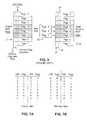
- FIG. 1shows a typical flash memory device internal architecture.
- the primary featuresinclude an input/output (I/O) bus 411 and control signals 412 to interface to an external controller, a memory control circuit 450 to control internal memory operations with registers for command, address and status signals.
- One or more arrays 400 of flash EEPROM cellsare included, each array having its own row decoder (XDEC) 401 and column decoder (YDEC) 402 , a group of sense amplifiers and program control circuitry (SA/PROG) 454 and a data register 404 .
- the memory cellsusually include one or more conductive floating gates as storage elements but other long term electron charge storage elements may be used instead.
- the memory cell arraymay be operated with two levels of charge defined for each storage element to therefore store one bit of data with each element. Alternatively, more than two storage states may be defined for each storage element, in which case more than one bit of data is stored in each element.
- a plurality of arrays 400together with related X decoders, Y decoders, program/verified circuitry, data registers, and the like are provided, for example as taught by U.S. Pat. No. 5,890,192, issued Mar. 30, 1999, and assigned to Sandisk Corporation, the assignee of this application, which is hereby incorporated by this reference.
- Related memory system featuresare described in co-pending patent application Ser. No. 09/505,555, filed Feb. 17, 2000 by Kevin Conley et al., which application is expressly incorporated herein by this reference.
- the external interface I/O bus 411 and control signals 412can include the following:
- FIG. 1shows only one flash memory array 400 with its related components, but a multiplicity of such arrays can exist on a single flash memory chip that share a common interface and memory control circuitry but have separate XDEC, YDEC, SA/PROG and DATA REG circuitry in order to allow parallel read and program operations.
- Datais transferred from the memory array through the data register 404 to an external controller via the data registers' coupling to the I/O bus AD[7:0] 411 .
- the data register 404is also coupled the sense amplifier/programming circuit 454 .
- the number of elements of the data register coupled to each sense amplifier/programming circuit elementmay depend on the number of bits stored in each storage element of the memory cells, flash EEPROM cells each containing one or more floating gates as the storage elements.
- Each storage elementmay store a plurality of bits, such as 2 or 4, if the memory cells are operated in a multi-state mode. Alternatively, the memory cells may be operated in a binary mode to store one bit of data per storage element.
- the row decoder 401decodes row addresses for the array 400 in order to select the physical page to be accessed.
- the row decoder 401receives row addresses via internal row address lines 419 from the memory control logic 450 .
- a column decoder 402receives column addresses via internal column address lines 429 from the memory control logic 450 .
- FIG. 2shows an architecture of a typical non-volatile data storage system, in this case employing flash memory cells as the storage media.
- this systemis encapsulated within a removable card having an electrical connector extending along one side to provide the host interface when inserted into a receptacle of a host.
- the system of FIG. 2may be embedded into a host system in the form of a permanently installed embedded circuit or otherwise.
- the systemutilizes a single controller 301 that performs high level host and memory control functions.
- the flash memory mediais composed of one or more flash memory devices, each such device often formed on its own integrated circuit chip.
- the system controller and the flash memoryare connected by a bus 302 that allows the controller 301 to load command, address, and transfer data to and from the flash memory array.
- the controller 301interfaces with a host system (not shown) with which user data is transferred to and from the flash memory array.
- the host interfaceincludes a mating plug and socket assembly (not shown) on the card and host equipment.
- the controller 301receives a command from the host to read or write one or more sectors of user data starting at a particular logical address. This address may or may not align with a boundary of a physical block of memory cells.
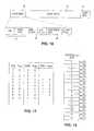
- FIG. 4wherein two of a large number of blocks of memory are included.
- One block 11(PBN 0 ) is illustrated to be divided into 8 pages for storing one sector of user data in each of its pages.
- Overhead data fields contained within each pageinclude a field 13 containing the LBN of the block 11 .
- the order of the logical pages within a logical blockis fixed with respect to the corresponding physical pages within a physical block.
- a second similarly configured block 15(PBN 1 ) is selected from an inventory of unused, erased blocks.
- Data within pages 3 - 5 of the original block 11are being updated by three pages of new data 17 .
- the new datais written into the corresponding pages 3 - 5 of the new block 15 , and user data from pages 0 - 2 , 6 and 7 of the block 11 are copied into corresponding pages of the new block 15 .
- All pages of the new block 15are preferably programmed in a single sequence of programming operations.
- the original block 11can be erased and placed in inventory for later use.
- the copying of data between the blocks 11 and 15which involves reading the data from one or more pages in the original block and subsequently programming the same data to pages in a newly assigned block, greatly reduces the write performance and usable lifetime of the storage system.
- partial tablesshow mapping of the logical blocks into the original and new physical blocks 11 and 15 before ( FIG. 5A ) and after ( FIG. 5B ) the updating of data described with respect to FIG. 4 .
- the original block 11stores pages 0 - 7 of LBN 0 into corresponding pages 0 - 7 of PBN 0 .
- the new block 15stores pages 0 - 7 of LBN 0 in corresponding pages 0 - 7 of PBN 1 . Receipt of a request to read data from LBN 0 is then directed to the physical block 15 instead of the physical block 11 .
- a table in the form of that shown in FIGS. 5A and 5Bis built from the LBN field 13 read from a physical page and knowledge of the PBN that is addressed when reading the data field 13 .
- the tableis usually stored in a volatile memory of the controller for ease of access, although only a portion of a complete table for the entire system is typically stored at any one time.
- a portion of the tableis usually formed immediately in advance of a read or programming operation that involves the blocks included in the table portion.
- flagsare recorded with the user data in pages and are used to indicate that pages of data in the original block that are being superceded by the newly written data are invalid. Only the new data is written to the newly assigned block. Thus the data in pages of the block not involved in the write operation but contained in the same physical block as the superceded data need not be copied into the new block.
- This operationis illustrated in FIG. 6 , where pages 3 - 5 of data within an original block 21 (PBN 0 ) are again being updated. Updated pages 3 - 5 of data 23 are written into corresponding pages of a new block 25 .
- an old/new flag 27is written in each of the pages 3 - 5 to indicate the data of those pages is old, while the flag 27 for the remaining pages 0 - 2 , 6 and 7 remains set at “new”.
- the new PBN 1is written into another overhead data field of each of the pages 3 - 5 in the block 21 to indicate where the updated data are located.
- the LBN and pageare stored in a field 31 within each of the physical pages.
- FIGS. 7A and 7Bare tables of the correspondence between the data LBN/page and the PBN/page before ( FIG. 7A ) and after ( FIG. 7B ) the data update is complete.
- the unchanged pages 0 - 2 , 6 and 7 of the LBNremain mapped into PBN 0 while the updated pages 3 - 5 are shown to reside in PBN 1 .
- the table of FIG. 7Bis built by the memory controller by reading the overhead data fields 27 , 29 and 31 of the pages within the block PBN 0 after the data update. Since the flag 27 is set to “old” in each of pages 3 - 5 of the original block PBN 0 , that block will no longer appear in the table for those pages.
- the new block number PBN 1appears instead, having been read from the overhead fields 29 ′ of the updated pages.
- the user data stored in the pages listed in the right column of FIG. 7Bare read and then assembled in the order shown for transfer to the host.
- Various flagsare typically located in the same physical page as the other associated overhead data, such as the LBN and an ECC.
- the memory arraymust have the capability that its pages can be programmed in at least at least two stages between erasures.
- the blockmust support the ability to program a page when other pages in the block with higher offsets or addresses have been already programmed.
- a limitation of some flash memorieshowever prevents the usage of such flags by specifying that the pages in a block can only be programmed in a physically sequential manner.
- the pagessupport a finite number of program cycles and in some cases additional programming of programmed pages is not permitted.
- flash EEPROMFlash EEPROM
- An example memory system where this has been found to be a problemis a NAND type, where a column of memory cells is formed as a series circuit string between a bit line and a common potential. Each word line extends across a row of memory cells formed of one cell in each such string.
- Such a memoryis particularly susceptible to such memory state disturbs when being operated in a multi-state mode to store more than one bit of data in each such cell.
- Such operationdivides an available window of a memory cell transistor threshold voltage range into narrow non-overlapping voltage level ranges, each range becoming narrower as the number of levels, and thus the number of bits being stored in each cell, are increased. For example, if four threshold ranges are used, two bits of data are stored in each cell's storage element.
- LBNlogical block number
- PBNsphysical block numbers
- One blockis the original block and the other contains the updated page data.
- Dataare written to the page location in the block corresponding to the low order bits of its logical address (LBA). This mapping is typical in various types of memory systems.
- pages containing updated dataare also assigned the same LBN and page offsets as the pages whose data has been superceded.
- the memory controllerdistinguishes the pages containing the superceded data from those containing the new, updated version either (1) by keeping track of the order in which the pages having the same logical addresses were written, such as by use of a counter, and/or (2) from the physical page addresses wherein, when pages are written in order within blocks from the lowest page address to the highest, the higher physical address contains the most recent copy of the data.
- the datais accessed for reading, therefore, those in the most current pages are used in cases where there are pages containing superceded data that have the same logical addresses, while the superceded data are ignored.
- FIGS. 8 and 9A first specific implementation of this technique is described with respect to FIGS. 8 and 9 .
- the situationis the same in this example as that in the prior art techniques described with respect to FIGS. 4-7B , namely the partial re-write of data within a block 35 , although each block is now shown to contain 16 pages.
- New data 37 for each of the pages 3 - 5 of the block 35 (PBN 35 )is written into three pages of a new block 39 (PBN 1 ) that has previously been erased, similar to that described previously.
- a LBN and page offset overhead data field 41 written into the pages of PBN 1 that contain the updated datais the same as that in the pages of the superceded data in the initial block PBN 0 .
- the logical LBN and page offsets, in the first column,are mapped into both the first physical block (PBN 0 ), in the second column, and, for the pages that have been updated, also into the second physical block (PBN 1 ) in the third column.
- the LBN and logical page offsets 41 ′ written into each of the three pages of updated data within the new block PBN 1are the same as those 41 written into each of a corresponding logical page of the original block PBN 0 .
- each pagecontains another overhead field 43 that provides an indication of its time of programming, at least relative to the time that other pages with the same logical address are programmed. This allows the controller to determine, when reading the data from the memory, the relative ages of the pages of data that are assigned the same logical address.
- the field 43which contains a form of time stamp
- the most straight forward wayis to record in that field, when the data of its associated page is programmed, the output of a real-time clock in the system. Later programmed pages with the same logical address then have a later time recorded in the field 43 . But when such a real-time clock is not available in the system, other techniques can be used.
- One specific techniqueis to store the output of a modulo-N counter as the value of the field 43 .
- the range of the countershould be one more than the number of pages that are contemplated to be stored with the same logical page number.
- the controllerWhen updating the data of a particular page in the original block PBN 0 , for example, the controller first reads the count stored in the field 43 of the page whose data are being updated, increments the count by some amount, such as one, and then writes that incremented count in the new block PBN 1 as the field 43 ′.
- the counterupon reaching a count of N+1, rolls over to 0. Since the number of blocks with the same LBN is less than N, there is always a point of discontinuity in the values of stored counts. It is easy then to handle the rollover with normalized to the point of discontinuity.
- the controllerwhen called upon to read the data, easily distinguishes between the new and superceded pages' data by comparing the counts in the fields 43 and 43 ′ of pages having the same LBA and page offset.
- data from the identified new pagesare then assembled, along with original pages that have not been updated, into the most recent version of the data file.
- the new data pages 37are stored in the first three pages 0 - 2 of the new block PBN 1 , rather than in the same pages 3 - 5 which they replace in the original block PBN 0 .
- the updated dataneed not necessarily be stored in the same page offset of the new block as that of the old block where superceded data is contained.
- Page(s) of updated datacan also be written to erased pages of the same block as the page of data being superceded.
- one NAND systemrequires that the pages within the blocks be programmed in sequential order. That means that programming of the middle pages 3 - 5 , as done in the new block 25 ( FIG. 6 ), wastes the pages 0 - 2 , which cannot later be programmed.
- the new data 37By storing the new data 37 in the first available pages of the new block 39 ( FIG. 8 ) in such a restrictive system, the remaining pages 3 - 7 are available for later use to store other data.
- FIG. 10An example of the structure of data stored in an individual page of the blocks of FIG. 8 is shown in FIG. 10 .
- the largest partis user data 45 .
- An error correction code (ECC) 47 calculated from the user datais also stored in the page.
- Overhead data 49including the LBN and page tag 41 (logical page offset), the time stamp 43 and an ECC 51 calculated from the overhead data are also stored in the page.
- ECC 50By having an ECC 50 covering the overhead data that is separate from the user data ECC 47 , the overhead 49 may be read separately from the user data and evaluated as valid without the need to transfer all of the data stored in the page. Alternatively, however, where the separate reading of the overhead data 49 is not a frequent event, all of the data in the page may be covered by a single ECC in order to reduce the total number of bits of ECC in a page.
- time stampis used only to determine the relative age of the data stored in blocks, while the most recent pages among those that carry the same LBN and page number are determined by their relative physical locations.
- the time stamp 43then does not need to be stored as part of each page. Rather, a single time stamp can be recorded for each block, either as part of the block or elsewhere within the non-volatile memory, and is updated each time a page of data is written into the block. Data is then read from pages in an order of descending physical address, starting from the last page of the most recently updated block containing data pages having the same LBN.
- the pagesare first read in the new block PBN 1 from the last (page 15 ) to the first (page 0 ), followed by reading the pages of the original block PBN 0 in the same reverse order.
- the superceded data in those pages of the original block PBN 0 that are identified by the same logical page numberscan be skipped during the reading process.
- physical pages 3 , 4 and 5 of the old block PBN 0are skipped during reading, in this example, once the controller determines that their LBN/pages 41 are the same as those of the pages already read from the new block PBN 1 .
- This processcan increase the speed of reading and reduce the number of overhead bits 49 that need to be stored for each page. Further, when this reverse page reading technique is employed, the table of FIG. 9 used by the controller during a reading operation can be simplified into the form of FIGS. 5A and 5B . Only an identity of those physical blocks containing data of a common logical block and the relative times that the physical blocks were programmed need to be known in order to carry out this efficient reading process.
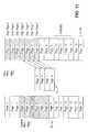
- FIG. 11illustrates an extension of the example of FIG. 8 by including a second update to the data originally written in the block PBN 0 .
- New data 51 for logical pages 5 , 6 , 7 and 8is written to the respective physical pages 3 , 4 , 5 and 6 of the new block PBN 1 , along with their LBN and page number. Note, in this example, that the data of logical page 5 is being updated for the second time.
- the most recently written logical pages 8 , 7 , 6 and 5 of the data of interestare first read in that order.
- the LBN/page overhead field in physical page 2 of PBN 1is the same as that read from the physical page 3 , so the user data of page 2 is not read.
- the physical pages 1 and 0are then read.
- the pages of the original block PBN 0are read, beginning with physical page 15 .
- the controllerwill note that the LBN/page fields of each of pages 8 - 3 match those of pages whose data has already been read, so the old data need not be read from those pages. The efficiency of the reading process is thus improved.
- the original data of physical pages 2 - 0are read since that data was not updated.
- this example of reading pages in a reverse orderefficiently sorts out the new data pages from the superceded data pages because data are written in physical page locations of an erased block in order from page 0 on.
- This techniqueis not limited to use with a memory system having such a specific programming constraint, however. So long as the order in which pages are programmed within a given block is known, the data from those pages may be read in the reverse order from which they were written. What is desired is that the most recently programmed pages having a common LBN with others that were earlier programmed be read first, and these are the most recently programmed pages. The most recent versions of updated pages are read first so that the superceded versions may easily be identified thereafter.
- FIG. 12A table showing the correspondence between the logical data and physical page addresses for the example of FIG. 11 is given in FIG. 12 .
- the table of FIG. 12constructed by reading the overhead data from each of the pages in blocks to which data of a common LBN has been written, can be used by the first implementation when the reverse page reading technique is not used.
- the table of FIG. 12need be built only to identify a correspondence between an LBN and all PBNs containing data of that LBN.
- FIG. 13An efficient way to organize pages of data being read from a physical block, where one or more of the pages has been updated, is illustrated by FIG. 13 .
- Enough spaceis provided in a volatile memory of the controller to buffer at least several pages of data at a time, and preferably a full block of data. That is what is shown in FIG. 13 .
- Sixteen pages of dataequal to the amount stored in a non-volatile memory block, are stored in the controller memory. Since the pages are most commonly read out of order, each page of data is stored in its proper position with respect to the other pages. For example, in the reverse page read operation of FIG. 11 , logical page 8 if the first to be read, so it is stored in position 8 of the controller memory, as indicated by the “1” in a circle.
- the nextis logical page 7 , and so forth, until all pages of data desired by the host are read and stored in the controller memory.
- the entire set of page datais then transferred to the host without having to manipulate the order of the data in the buffer memory.
- the pages of datahave already be organized by writing them to the proper location in the controller memory.
- a method of programming a non-volatile memory system that utilizes the techniques described with respect to FIGS. 8 and 9is illustrated in the flow chart of FIG. 14 .
- Data for pages of an existing file to be updatedare received from a host system, as indicated by the block 52 . It is first determined by a step 53 whether the number of pages of updated data to be stored is equal to or greater than the storage capacity of a block of the system, 16 pages being shown as the block capacity, for simplicity, in the above described example. If so, one or more unused, erased blocks are addressed, in a step 55 , and the new data pages are written to the addressed block(s), in a step 57 .
- the updating of one block or more of datawill result in one or more blocks storing the data that have been superceded by the new data. If so, as indicated by a step 59 , those blocks with superceded data are identified for erasure. For the purpose of increasing performance, it is preferable that erase operations occur in the background, or when host requested programming or reading operations are not taking place. After being erased, the blocks are returned to the inventory of unused, erased blocks for further use. Alternatively, erasure of the blocks can be deferred until they are needed for programming operations.
- a next step 61determines whether there are enough unused pages in a block having some pages programmed with other data. If so, such a block is addressed, in a step 63 . If not, a totally unused, erased block is addressed, in a step 65 . In either case, in a step 67 , the new data are programmed into unused pages of the addressed block. As part of this programming process, the LBN and page offset is written into the fields 41 , and the time stamp into the fields 43 of each of the pages ( FIG. 8 ) of the updated data, in the manner described above.
- a desirable feature of the programming processis to make available for future programming any blocks that store only superceded data. So the question is asked, in a step 69 , whether the data updating process has resulted in an entire block remaining with only superceded data. If so, such a block is queued for erasure, in a step 71 , and the process is then completed. If not, the step 71 is omitted and the data update is finished.
- One implementationdivides the memory array into largely independent sub-arrays or units, such as multiple units 80 - 83 of FIG. 15 , each unit in turn being divided into a large number of blocks, as shown. Pages of data are then programmed at the same time into more than one of the units.
- Another configurationfurther combines one or more of these units from multiple memory chips. These multiple chips may be connected to a single bus (as shown in FIG. 2 ) or multiple independent busses for higher data throughput. An extension of this is to link blocks from different units for programming, reading and erasing together, an example being shown in FIG. 15 .
- Blocks 85 - 88 from respective ones of the units 80 - 83can be operated together as a metablock, for example.
- each blockthe smallest erasable group of the memory array, is typically divided into multiple pages, a page containing the smallest number of cells that are programmable together within the block. Therefore, a programming operation of the metablock shown in FIG. 15 will usually include the simultaneously programming of data into at least one page of each of the blocks 85 - 88 forming the metablock, which is repeated until the metablock is full or the incoming data has all been programmed.
- Other metablocksare formed of different blocks from the array units, one block from each unit.
- pages of data less than an entire blockoften need to be updated. This can be done for individual blocks of a metablock in the same manner as described above with respect to either of FIG. 4 or 6 , but preferably by use of the improved technique described with respect to FIG. 8 .
- an additional block of memory within the same unitis also used.
- a data updatemay require writing new data for one or more pages of two or more of the blocks of a metablock. This can then require use of up to four additional blocks 90 - 93 , one in each of the four units, to update a data file stored in the metablock, even though the data in only a few pages is being updated.
- updates to pages of data within any of the blocks of the illustrated metablockare made, as illustrated by FIG. 16 , to a single additional block 90 in the memory unit 80 , so long as unused pages in the block 80 remain. If, for example, data in three pages of the block 86 and two pages of the block 88 are being updated at one time, all five pages of the new data are written into the block 90 . This can save the use of one block of memory, thereby to effectively increase the number of available erased blocks by one block. This helps avoid, or at least postpone, the time when an inventory of erased blocks becomes exhausted.
Landscapes
- Engineering & Computer Science (AREA)
- Theoretical Computer Science (AREA)
- Physics & Mathematics (AREA)
- General Engineering & Computer Science (AREA)
- General Physics & Mathematics (AREA)
- Computer Security & Cryptography (AREA)
- Read Only Memory (AREA)
- Techniques For Improving Reliability Of Storages (AREA)
- Memory System (AREA)
- Non-Volatile Memory (AREA)
Abstract
Description
- CS—Chip Select. Used to activate flash memory interface.
- RS—Read Strobe. Used to indicate the I/O bus is being used to transfer data from the memory array.
- WS—Write Strobe. Used to indicate the I/O bus is being used to transfer data to the memory array.
- AS—Address Strobe. Indicates that the I/O bus is being used to transfer address information.
- AD[7:0]—Address/Data Bus This I/O bus is used to transfer data between controller and the flash memory command, address and data registers of the
memory control 450.
Claims (16)
Priority Applications (2)
| Application Number | Priority Date | Filing Date | Title |
|---|---|---|---|
| US12/900,397US7970987B2 (en) | 2001-01-19 | 2010-10-07 | Partial block data programming and reading operations in a non-volatile memory |
| US13/168,756US8316177B2 (en) | 2001-01-19 | 2011-06-24 | Partial block data programming and reading operations in a non-volatile memory |
Applications Claiming Priority (4)
| Application Number | Priority Date | Filing Date | Title |
|---|---|---|---|
| US09/766,436US6763424B2 (en) | 2001-01-19 | 2001-01-19 | Partial block data programming and reading operations in a non-volatile memory |
| US10/841,388US6968421B2 (en) | 2001-01-19 | 2004-05-07 | Partial block data programming and reading operations in a non-volatile memory |
| US11/250,238US7818490B2 (en) | 2001-01-19 | 2005-10-13 | Partial block data programming and reading operations in a non-volatile memory |
| US12/900,397US7970987B2 (en) | 2001-01-19 | 2010-10-07 | Partial block data programming and reading operations in a non-volatile memory |
Related Parent Applications (1)
| Application Number | Title | Priority Date | Filing Date |
|---|---|---|---|
| US11/250,238ContinuationUS7818490B2 (en) | 2001-01-19 | 2005-10-13 | Partial block data programming and reading operations in a non-volatile memory |
Related Child Applications (1)
| Application Number | Title | Priority Date | Filing Date |
|---|---|---|---|
| US13/168,756ContinuationUS8316177B2 (en) | 2001-01-19 | 2011-06-24 | Partial block data programming and reading operations in a non-volatile memory |
Publications (2)
| Publication Number | Publication Date |
|---|---|
| US20110029724A1 US20110029724A1 (en) | 2011-02-03 |
| US7970987B2true US7970987B2 (en) | 2011-06-28 |
Family
ID=25076410
Family Applications (6)
| Application Number | Title | Priority Date | Filing Date |
|---|---|---|---|
| US09/766,436Expired - LifetimeUS6763424B2 (en) | 2001-01-19 | 2001-01-19 | Partial block data programming and reading operations in a non-volatile memory |
| US10/841,388Expired - LifetimeUS6968421B2 (en) | 2001-01-19 | 2004-05-07 | Partial block data programming and reading operations in a non-volatile memory |
| US11/250,238Expired - Fee RelatedUS7818490B2 (en) | 2001-01-19 | 2005-10-13 | Partial block data programming and reading operations in a non-volatile memory |
| US12/371,460Expired - Fee RelatedUS7657702B2 (en) | 2001-01-19 | 2009-02-13 | Partial block data programming and reading operations in a non-volatile memory |
| US12/900,397Expired - Fee RelatedUS7970987B2 (en) | 2001-01-19 | 2010-10-07 | Partial block data programming and reading operations in a non-volatile memory |
| US13/168,756Expired - Fee RelatedUS8316177B2 (en) | 2001-01-19 | 2011-06-24 | Partial block data programming and reading operations in a non-volatile memory |
Family Applications Before (4)
| Application Number | Title | Priority Date | Filing Date |
|---|---|---|---|
| US09/766,436Expired - LifetimeUS6763424B2 (en) | 2001-01-19 | 2001-01-19 | Partial block data programming and reading operations in a non-volatile memory |
| US10/841,388Expired - LifetimeUS6968421B2 (en) | 2001-01-19 | 2004-05-07 | Partial block data programming and reading operations in a non-volatile memory |
| US11/250,238Expired - Fee RelatedUS7818490B2 (en) | 2001-01-19 | 2005-10-13 | Partial block data programming and reading operations in a non-volatile memory |
| US12/371,460Expired - Fee RelatedUS7657702B2 (en) | 2001-01-19 | 2009-02-13 | Partial block data programming and reading operations in a non-volatile memory |
Family Applications After (1)
| Application Number | Title | Priority Date | Filing Date |
|---|---|---|---|
| US13/168,756Expired - Fee RelatedUS8316177B2 (en) | 2001-01-19 | 2011-06-24 | Partial block data programming and reading operations in a non-volatile memory |
Country Status (11)
| Country | Link |
|---|---|
| US (6) | US6763424B2 (en) |
| EP (4) | EP1645964A3 (en) |
| JP (3) | JP4155824B2 (en) |
| KR (2) | KR101076830B1 (en) |
| CN (3) | CN1290021C (en) |
| AT (1) | ATE327556T1 (en) |
| AU (1) | AU2002236723A1 (en) |
| DE (1) | DE60211653T2 (en) |
| ES (1) | ES2262782T3 (en) |
| TW (1) | TWI221217B (en) |
| WO (1) | WO2002058074A2 (en) |
Cited By (5)
| Publication number | Priority date | Publication date | Assignee | Title |
|---|---|---|---|---|
| US20100177250A1 (en)* | 2007-06-01 | 2010-07-15 | Hiromasa Hoshino | Recording apparatus and recording method |
| US9116793B2 (en) | 2012-06-12 | 2015-08-25 | International Business Machines Corporation | Maintaining versions of data in solid state memory |
| US9122582B2 (en) | 2012-06-12 | 2015-09-01 | International Business Machines Corporation | File system for maintaining data versions in solid state memory |
| US9122581B2 (en) | 2012-06-12 | 2015-09-01 | International Business Machines Corporation | Data versioning in solid state memory |
| US9135161B2 (en) | 2012-06-12 | 2015-09-15 | International Business Machines Corporation | Flash translation layer system for maintaining data versions in solid state memory |
Families Citing this family (456)
| Publication number | Priority date | Publication date | Assignee | Title |
|---|---|---|---|---|
| US5657332A (en)* | 1992-05-20 | 1997-08-12 | Sandisk Corporation | Soft errors handling in EEPROM devices |
| JP3215237B2 (en)* | 1993-10-01 | 2001-10-02 | 富士通株式会社 | Storage device and method for writing / erasing storage device |
| KR100544175B1 (en)* | 1999-05-08 | 2006-01-23 | 삼성전자주식회사 | Recording medium and defect area processing method for storing linking type information |
| US6426893B1 (en)* | 2000-02-17 | 2002-07-30 | Sandisk Corporation | Flash eeprom system with simultaneous multiple data sector programming and storage of physical block characteristics in other designated blocks |
| US6763424B2 (en) | 2001-01-19 | 2004-07-13 | Sandisk Corporation | Partial block data programming and reading operations in a non-volatile memory |
| CA2452534A1 (en)* | 2001-07-03 | 2003-01-16 | Research In Motion Limited | System and method of object-oriented persistence |
| US7108975B2 (en)* | 2001-09-21 | 2006-09-19 | Regents Of The University Of Michigan | Atlastin |
| KR100449708B1 (en)* | 2001-11-16 | 2004-09-22 | 삼성전자주식회사 | Flash memory management method |
| US6871257B2 (en) | 2002-02-22 | 2005-03-22 | Sandisk Corporation | Pipelined parallel programming operation in a non-volatile memory system |
| JP2004062554A (en)* | 2002-07-30 | 2004-02-26 | Oki Electric Ind Co Ltd | Managing method of flash memory |
| JP4358111B2 (en)* | 2002-08-29 | 2009-11-04 | パナソニック株式会社 | Semiconductor memory device and data writing method to flash memory |
| US7039788B1 (en) | 2002-10-28 | 2006-05-02 | Sandisk Corporation | Method and apparatus for splitting a logical block |
| EP1556868B1 (en)* | 2002-10-28 | 2007-09-05 | SanDisk Corporation | Automated wear leveling in non-volatile storage systems |
| US7234036B1 (en) | 2002-10-28 | 2007-06-19 | Sandisk Corporation | Method and apparatus for resolving physical blocks associated with a common logical block |
| US7254668B1 (en)* | 2002-10-28 | 2007-08-07 | Sandisk Corporation | Method and apparatus for grouping pages within a block |
| DE10252059B3 (en)* | 2002-11-08 | 2004-04-15 | Infineon Technologies Ag | Data memory operating method e.g. for portable data carrier or mobile data processor, using back-up memory for retaining memory cell contents upon current interruption during programming |
| US7478248B2 (en)* | 2002-11-27 | 2009-01-13 | M-Systems Flash Disk Pioneers, Ltd. | Apparatus and method for securing data on a portable storage device |
| EP1435576B1 (en)* | 2003-01-03 | 2013-03-20 | Austria Card Plastikkarten und Ausweissysteme GmbH | Method and apparatus for block-oriented memory management provided in smart card controllers |
| US6944063B2 (en) | 2003-01-28 | 2005-09-13 | Sandisk Corporation | Non-volatile semiconductor memory with large erase blocks storing cycle counts |
| JP2004265162A (en)* | 2003-03-03 | 2004-09-24 | Renesas Technology Corp | Storage device and address management method |
| KR100526178B1 (en)* | 2003-03-31 | 2005-11-03 | 삼성전자주식회사 | Access apparatus and method using flash memory |
| US20040228411A1 (en)* | 2003-05-12 | 2004-11-18 | Sony Corporation | Method and system for decoder clock control in presence of jitter |
| US7117326B2 (en)* | 2003-06-26 | 2006-10-03 | Intel Corporation | Tracking modifications to a memory |
| US6891740B2 (en)* | 2003-08-29 | 2005-05-10 | Hitachi Global Storage Technologies Netherlands B.V. | Method for speculative streaming data from a disk drive |
| US7188228B1 (en) | 2003-10-01 | 2007-03-06 | Sandisk Corporation | Hybrid mapping implementation within a non-volatile memory system |
| US7012835B2 (en)* | 2003-10-03 | 2006-03-14 | Sandisk Corporation | Flash memory data correction and scrub techniques |
| US7173852B2 (en)* | 2003-10-03 | 2007-02-06 | Sandisk Corporation | Corrected data storage and handling methods |
| JP2005128771A (en)* | 2003-10-23 | 2005-05-19 | Fujitsu Ltd | Data file system, data access server, and data access program |
| DE10349595B3 (en)* | 2003-10-24 | 2004-12-09 | Hyperstone Ag | Writing sectors of block-deletable memory, writes to alternative memory block sectors in sequence, storing their positions in sector table |
| KR100608602B1 (en)* | 2003-12-10 | 2006-08-03 | 삼성전자주식회사 | Flash memory, mapping control device and method therefor |
| JP2005190288A (en)* | 2003-12-26 | 2005-07-14 | Tdk Corp | Memory controller, flash memory system therewith, and method for controlling flash memory |
| US20050144363A1 (en)* | 2003-12-30 | 2005-06-30 | Sinclair Alan W. | Data boundary management |
| US7433993B2 (en)* | 2003-12-30 | 2008-10-07 | San Disk Corportion | Adaptive metablocks |
| US8504798B2 (en)* | 2003-12-30 | 2013-08-06 | Sandisk Technologies Inc. | Management of non-volatile memory systems having large erase blocks |
| US7383375B2 (en)* | 2003-12-30 | 2008-06-03 | Sandisk Corporation | Data run programming |
| US7173863B2 (en) | 2004-03-08 | 2007-02-06 | Sandisk Corporation | Flash controller cache architecture |
| US7631138B2 (en)* | 2003-12-30 | 2009-12-08 | Sandisk Corporation | Adaptive mode switching of flash memory address mapping based on host usage characteristics |
| US20050144516A1 (en)* | 2003-12-30 | 2005-06-30 | Gonzalez Carlos J. | Adaptive deterministic grouping of blocks into multi-block units |
| WO2005066792A2 (en)* | 2003-12-30 | 2005-07-21 | Sandisk Corporation | Non-volatile memory and method with memory planes alignment |
| US7139864B2 (en)* | 2003-12-30 | 2006-11-21 | Sandisk Corporation | Non-volatile memory and method with block management system |
| KR100526188B1 (en)* | 2003-12-30 | 2005-11-04 | 삼성전자주식회사 | Method for address mapping and managing mapping information, and flash memory thereof |
| DE102004005290B3 (en)* | 2004-02-03 | 2005-07-21 | Giesecke & Devrient Gmbh | Securing data in non-volatile data memory divided into segments involves management data per segment containing further data element to determine age range of second segment data compared to first segment data for incomplete clearing |
| US7136973B2 (en) | 2004-02-04 | 2006-11-14 | Sandisk Corporation | Dual media storage device |
| US7127549B2 (en) | 2004-02-04 | 2006-10-24 | Sandisk Corporation | Disk acceleration using first and second storage devices |
| KR100526190B1 (en)* | 2004-02-06 | 2005-11-03 | 삼성전자주식회사 | Remapping method for flash memory |
| US7529904B2 (en)* | 2004-03-31 | 2009-05-05 | International Business Machines Corporation | Storing location identifier in array and array pointer in data structure for write process management |
| US7325090B2 (en) | 2004-04-29 | 2008-01-29 | Sandisk Il Ltd. | Refreshing data stored in a flash memory |
| US7490283B2 (en) | 2004-05-13 | 2009-02-10 | Sandisk Corporation | Pipelined data relocation and improved chip architectures |
| JP4253272B2 (en)* | 2004-05-27 | 2009-04-08 | 株式会社東芝 | Memory card, semiconductor device, and control method of semiconductor memory |
| US8429313B2 (en)* | 2004-05-27 | 2013-04-23 | Sandisk Technologies Inc. | Configurable ready/busy control |
| US7395384B2 (en) | 2004-07-21 | 2008-07-01 | Sandisk Corproation | Method and apparatus for maintaining data on non-volatile memory systems |
| US8607016B2 (en)* | 2004-07-21 | 2013-12-10 | Sandisk Technologies Inc. | FAT analysis for optimized sequential cluster management |
| US8375146B2 (en) | 2004-08-09 | 2013-02-12 | SanDisk Technologies, Inc. | Ring bus structure and its use in flash memory systems |
| JP3942612B2 (en)* | 2004-09-10 | 2007-07-11 | 東京エレクトロンデバイス株式会社 | Storage device, memory management method, and program |
| JP4586469B2 (en)* | 2004-09-15 | 2010-11-24 | ソニー株式会社 | MEMORY CONTROL DEVICE, MEMORY CONTROL METHOD, PROGRAM |
| KR100624960B1 (en)* | 2004-10-05 | 2006-09-15 | 에스티마이크로일렉트로닉스 엔.브이. | Semiconductor memory device and its package and memory card using the same |
| US7441067B2 (en) | 2004-11-15 | 2008-10-21 | Sandisk Corporation | Cyclic flash memory wear leveling |
| US7120051B2 (en) | 2004-12-14 | 2006-10-10 | Sandisk Corporation | Pipelined programming of non-volatile memories using early data |
| US7420847B2 (en) | 2004-12-14 | 2008-09-02 | Sandisk Corporation | Multi-state memory having data recovery after program fail |
| US7158421B2 (en) | 2005-04-01 | 2007-01-02 | Sandisk Corporation | Use of data latches in multi-phase programming of non-volatile memories |
| US7315916B2 (en)* | 2004-12-16 | 2008-01-01 | Sandisk Corporation | Scratch pad block |
| US7366826B2 (en)* | 2004-12-16 | 2008-04-29 | Sandisk Corporation | Non-volatile memory and method with multi-stream update tracking |
| US7395404B2 (en)* | 2004-12-16 | 2008-07-01 | Sandisk Corporation | Cluster auto-alignment for storing addressable data packets in a non-volatile memory array |
| US7386655B2 (en)* | 2004-12-16 | 2008-06-10 | Sandisk Corporation | Non-volatile memory and method with improved indexing for scratch pad and update blocks |
| US7412560B2 (en) | 2004-12-16 | 2008-08-12 | Sandisk Corporation | Non-volatile memory and method with multi-stream updating |
| US8122193B2 (en) | 2004-12-21 | 2012-02-21 | Samsung Electronics Co., Ltd. | Storage device and user device including the same |
| US7409473B2 (en) | 2004-12-21 | 2008-08-05 | Sandisk Corporation | Off-chip data relocation |
| KR100669342B1 (en)* | 2004-12-21 | 2007-01-16 | 삼성전자주식회사 | How to Program Nand Flash Memory Devices |
| US7882299B2 (en)* | 2004-12-21 | 2011-02-01 | Sandisk Corporation | System and method for use of on-chip non-volatile memory write cache |
| US7849381B2 (en)* | 2004-12-21 | 2010-12-07 | Sandisk Corporation | Method for copying data in reprogrammable non-volatile memory |
| KR100684887B1 (en)* | 2005-02-04 | 2007-02-20 | 삼성전자주식회사 | Data storage device including flash memory and its merge method |
| US7212440B2 (en) | 2004-12-30 | 2007-05-01 | Sandisk Corporation | On-chip data grouping and alignment |
| KR100698655B1 (en) | 2005-01-04 | 2007-03-23 | 주식회사 팬택앤큐리텔 | The file update system of the mobile communication terminal, the boot management system of the mobile communication terminal to prevent fatal errors due to the loss of the EFS area header, the mobile communication terminal to prevent the fatal error due to the file update method and the loss of the EFS area header. How to boot the terminal |
| US7315917B2 (en)* | 2005-01-20 | 2008-01-01 | Sandisk Corporation | Scheduling of housekeeping operations in flash memory systems |
| US20060161724A1 (en)* | 2005-01-20 | 2006-07-20 | Bennett Alan D | Scheduling of housekeeping operations in flash memory systems |
| US20060184719A1 (en)* | 2005-02-16 | 2006-08-17 | Sinclair Alan W | Direct data file storage implementation techniques in flash memories |
| US20060184718A1 (en)* | 2005-02-16 | 2006-08-17 | Sinclair Alan W | Direct file data programming and deletion in flash memories |
| US9104315B2 (en) | 2005-02-04 | 2015-08-11 | Sandisk Technologies Inc. | Systems and methods for a mass data storage system having a file-based interface to a host and a non-file-based interface to secondary storage |
| US7877539B2 (en)* | 2005-02-16 | 2011-01-25 | Sandisk Corporation | Direct data file storage in flash memories |
| US7206230B2 (en) | 2005-04-01 | 2007-04-17 | Sandisk Corporation | Use of data latches in cache operations of non-volatile memories |
| US7447078B2 (en) | 2005-04-01 | 2008-11-04 | Sandisk Corporation | Method for non-volatile memory with background data latch caching during read operations |
| US7463521B2 (en) | 2005-04-01 | 2008-12-09 | Sandisk Corporation | Method for non-volatile memory with managed execution of cached data |
| EP1712984A1 (en)* | 2005-04-15 | 2006-10-18 | Deutsche Thomson-Brandt Gmbh | Method and system for accessing logical data blocks in a storage system that includes multiple memories which are connected to at least one common bus |
| US9384818B2 (en) | 2005-04-21 | 2016-07-05 | Violin Memory | Memory power management |
| CN103116565A (en) | 2005-04-21 | 2013-05-22 | 提琴存储器公司 | Configurable switching element, interconnection network and interconnection method among networks |
| US8200887B2 (en) | 2007-03-29 | 2012-06-12 | Violin Memory, Inc. | Memory management system and method |
| JP5130646B2 (en) | 2005-06-06 | 2013-01-30 | ソニー株式会社 | Storage device |
| US7797479B2 (en)* | 2005-06-30 | 2010-09-14 | Intel Corporation | Technique to write to a non-volatile memory |
| US7552271B2 (en) | 2005-08-03 | 2009-06-23 | Sandisk Corporation | Nonvolatile memory with block management |
| US7984084B2 (en)* | 2005-08-03 | 2011-07-19 | SanDisk Technologies, Inc. | Non-volatile memory with scheduled reclaim operations |
| US7480766B2 (en)* | 2005-08-03 | 2009-01-20 | Sandisk Corporation | Interfacing systems operating through a logical address space and on a direct data file basis |
| US7669003B2 (en)* | 2005-08-03 | 2010-02-23 | Sandisk Corporation | Reprogrammable non-volatile memory systems with indexing of directly stored data files |
| US7558906B2 (en) | 2005-08-03 | 2009-07-07 | Sandisk Corporation | Methods of managing blocks in nonvolatile memory |
| US7949845B2 (en)* | 2005-08-03 | 2011-05-24 | Sandisk Corporation | Indexing of file data in reprogrammable non-volatile memories that directly store data files |
| US7627733B2 (en) | 2005-08-03 | 2009-12-01 | Sandisk Corporation | Method and system for dual mode access for storage devices |
| KR100714873B1 (en)* | 2005-09-06 | 2007-05-07 | 삼성전자주식회사 | Method for updating data in nonvolatile memory and apparatus therefor |
| US8429326B2 (en) | 2005-09-12 | 2013-04-23 | Mediatek Inc. | Method and system for NAND-flash identification without reading device ID table |
| CN100375026C (en)* | 2005-09-13 | 2008-03-12 | 联想(北京)有限公司 | Quick storage equipment software installing/updating method |
| JP4751163B2 (en)* | 2005-09-29 | 2011-08-17 | 株式会社東芝 | Memory system |
| US20070089023A1 (en)* | 2005-09-30 | 2007-04-19 | Sigmatel, Inc. | System and method for system resource access |
| US7814262B2 (en)* | 2005-10-13 | 2010-10-12 | Sandisk Corporation | Memory system storing transformed units of data in fixed sized storage blocks |
| US7529905B2 (en)* | 2005-10-13 | 2009-05-05 | Sandisk Corporation | Method of storing transformed units of data in a memory system having fixed sized storage blocks |
| US7509471B2 (en)* | 2005-10-27 | 2009-03-24 | Sandisk Corporation | Methods for adaptively handling data writes in non-volatile memories |
| US7631162B2 (en) | 2005-10-27 | 2009-12-08 | Sandisck Corporation | Non-volatile memory with adaptive handling of data writes |
| US20070106842A1 (en)* | 2005-11-04 | 2007-05-10 | Conley Kevin M | Enhanced first level storage caching methods using nonvolatile memory |
| US7634585B2 (en)* | 2005-11-04 | 2009-12-15 | Sandisk Corporation | In-line cache using nonvolatile memory between host and disk device |
| US7447066B2 (en)* | 2005-11-08 | 2008-11-04 | Sandisk Corporation | Memory with retargetable memory cell redundancy |
| US7877540B2 (en)* | 2005-12-13 | 2011-01-25 | Sandisk Corporation | Logically-addressed file storage methods |
| US7730453B2 (en)* | 2005-12-13 | 2010-06-01 | Microsoft Corporation | Runtime detection for invalid use of zero-length memory allocations |
| US7747837B2 (en) | 2005-12-21 | 2010-06-29 | Sandisk Corporation | Method and system for accessing non-volatile storage devices |
| JP2009521049A (en)* | 2005-12-21 | 2009-05-28 | エヌエックスピー ビー ヴィ | Memory with block erasable storage locations |
| US20070143561A1 (en)* | 2005-12-21 | 2007-06-21 | Gorobets Sergey A | Methods for adaptive file data handling in non-volatile memories with a directly mapped file storage system |
| US20070156998A1 (en)* | 2005-12-21 | 2007-07-05 | Gorobets Sergey A | Methods for memory allocation in non-volatile memories with a directly mapped file storage system |
| US20070143566A1 (en)* | 2005-12-21 | 2007-06-21 | Gorobets Sergey A | Non-volatile memories with data alignment in a directly mapped file storage system |
| US20070143567A1 (en)* | 2005-12-21 | 2007-06-21 | Gorobets Sergey A | Methods for data alignment in non-volatile memories with a directly mapped file storage system |
| JP2009521045A (en)* | 2005-12-21 | 2009-05-28 | エヌエックスピー ビー ヴィ | Nonvolatile memory having block erasable memory locations |
| US7769978B2 (en)* | 2005-12-21 | 2010-08-03 | Sandisk Corporation | Method and system for accessing non-volatile storage devices |
| US7793068B2 (en) | 2005-12-21 | 2010-09-07 | Sandisk Corporation | Dual mode access for non-volatile storage devices |
| US20070143378A1 (en)* | 2005-12-21 | 2007-06-21 | Gorobets Sergey A | Non-volatile memories with adaptive file handling in a directly mapped file storage system |
| US7546515B2 (en)* | 2005-12-27 | 2009-06-09 | Sandisk Corporation | Method of storing downloadable firmware on bulk media |
| US7536627B2 (en)* | 2005-12-27 | 2009-05-19 | Sandisk Corporation | Storing downloadable firmware on bulk media |
| KR100772863B1 (en)* | 2006-01-13 | 2007-11-02 | 삼성전자주식회사 | Method and apparatus for shortening page replacement time in system applying demand paging technique |
| US7793059B2 (en)* | 2006-01-18 | 2010-09-07 | Apple Inc. | Interleaving policies for flash memory |
| US7609561B2 (en)* | 2006-01-18 | 2009-10-27 | Apple Inc. | Disabling faulty flash memory dies |
| US7752391B2 (en)* | 2006-01-20 | 2010-07-06 | Apple Inc. | Variable caching policy system and method |
| US20070174641A1 (en)* | 2006-01-25 | 2007-07-26 | Cornwell Michael J | Adjusting power supplies for data storage devices |
| US7702935B2 (en)* | 2006-01-25 | 2010-04-20 | Apple Inc. | Reporting flash memory operating voltages |
| TWI311327B (en)* | 2006-01-26 | 2009-06-21 | Nuvoton Technology Corporatio | Method for page random write and read in the block of flash memory |
| US7861122B2 (en)* | 2006-01-27 | 2010-12-28 | Apple Inc. | Monitoring health of non-volatile memory |
| US7594043B2 (en)* | 2006-01-27 | 2009-09-22 | Apple Inc. | Reducing dismount time for mass storage class devices |
| US7912994B2 (en)* | 2006-01-27 | 2011-03-22 | Apple Inc. | Reducing connection time for mass storage class peripheral by internally prefetching file data into local cache in response to connection to host |
| JP2007280108A (en)* | 2006-04-07 | 2007-10-25 | Sony Corp | Storage medium controller, storage medium control method, and program |
| US7849302B2 (en)* | 2006-04-10 | 2010-12-07 | Apple Inc. | Direct boot arrangement using a NAND flash memory |
| US7467253B2 (en)* | 2006-04-13 | 2008-12-16 | Sandisk Corporation | Cycle count storage systems |
| US7451264B2 (en)* | 2006-04-13 | 2008-11-11 | Sandisk Corporation | Cycle count storage methods |
| US7568135B2 (en) | 2006-05-15 | 2009-07-28 | Apple Inc. | Use of alternative value in cell detection |
| US7613043B2 (en)* | 2006-05-15 | 2009-11-03 | Apple Inc. | Shifting reference values to account for voltage sag |
| US7911834B2 (en)* | 2006-05-15 | 2011-03-22 | Apple Inc. | Analog interface for a flash memory die |
| US8000134B2 (en)* | 2006-05-15 | 2011-08-16 | Apple Inc. | Off-die charge pump that supplies multiple flash devices |
| US7701797B2 (en)* | 2006-05-15 | 2010-04-20 | Apple Inc. | Two levels of voltage regulation supplied for logic and data programming voltage of a memory device |
| US7551486B2 (en) | 2006-05-15 | 2009-06-23 | Apple Inc. | Iterative memory cell charging based on reference cell value |
| US7639542B2 (en)* | 2006-05-15 | 2009-12-29 | Apple Inc. | Maintenance operations for multi-level data storage cells |
| US7852690B2 (en)* | 2006-05-15 | 2010-12-14 | Apple Inc. | Multi-chip package for a flash memory |
| US7639531B2 (en)* | 2006-05-15 | 2009-12-29 | Apple Inc. | Dynamic cell bit resolution |
| US7511646B2 (en)* | 2006-05-15 | 2009-03-31 | Apple Inc. | Use of 8-bit or higher A/D for NAND cell value |
| JP4153535B2 (en)* | 2006-05-30 | 2008-09-24 | Tdk株式会社 | MEMORY CONTROLLER, FLASH MEMORY SYSTEM PROVIDED WITH MEMORY CONTROLLER, AND FLASH MEMORY CONTROL METHOD |
| US7567461B2 (en)* | 2006-08-18 | 2009-07-28 | Micron Technology, Inc. | Method and system for minimizing number of programming pulses used to program rows of non-volatile memory cells |
| US8001314B2 (en) | 2006-09-12 | 2011-08-16 | Apple Inc. | Storing a driver for controlling a memory |
| US7593259B2 (en)* | 2006-09-13 | 2009-09-22 | Mosaid Technologies Incorporated | Flash multi-level threshold distribution scheme |
| US7696044B2 (en)* | 2006-09-19 | 2010-04-13 | Sandisk Corporation | Method of making an array of non-volatile memory cells with floating gates formed of spacers in substrate trenches |
| US7646054B2 (en)* | 2006-09-19 | 2010-01-12 | Sandisk Corporation | Array of non-volatile memory cells with floating gates formed of spacers in substrate trenches |
| US7886204B2 (en)* | 2006-09-27 | 2011-02-08 | Sandisk Corporation | Methods of cell population distribution assisted read margining |
| US7716538B2 (en)* | 2006-09-27 | 2010-05-11 | Sandisk Corporation | Memory with cell population distribution assisted read margining |
| US20080091871A1 (en)* | 2006-10-12 | 2008-04-17 | Alan David Bennett | Non-volatile memory with worst-case control data management |
| US20080091901A1 (en)* | 2006-10-12 | 2008-04-17 | Alan David Bennett | Method for non-volatile memory with worst-case control data management |
| KR100771521B1 (en) | 2006-10-30 | 2007-10-30 | 삼성전자주식회사 | Flash memory device including multi-level cells and method of writing data thereof |
| US8151060B2 (en) | 2006-11-28 | 2012-04-03 | Hitachi, Ltd. | Semiconductor memory system having a snapshot function |
| US8019938B2 (en)* | 2006-12-06 | 2011-09-13 | Fusion-I0, Inc. | Apparatus, system, and method for solid-state storage as cache for high-capacity, non-volatile storage |
| US9495241B2 (en) | 2006-12-06 | 2016-11-15 | Longitude Enterprise Flash S.A.R.L. | Systems and methods for adaptive data storage |
| US9116823B2 (en) | 2006-12-06 | 2015-08-25 | Intelligent Intellectual Property Holdings 2 Llc | Systems and methods for adaptive error-correction coding |
| US8074011B2 (en)* | 2006-12-06 | 2011-12-06 | Fusion-Io, Inc. | Apparatus, system, and method for storage space recovery after reaching a read count limit |
| JP2008152464A (en)* | 2006-12-15 | 2008-07-03 | Toshiba Corp | Storage device |
| KR101354152B1 (en)* | 2006-12-18 | 2014-01-27 | 삼성전자주식회사 | Method for command scheduling of virtual file system embodied in non-volatile data storage and apparatus thereof |
| US7554855B2 (en)* | 2006-12-20 | 2009-06-30 | Mosaid Technologies Incorporated | Hybrid solid-state memory system having volatile and non-volatile memory |
| US7800161B2 (en)* | 2006-12-21 | 2010-09-21 | Sandisk Corporation | Flash NAND memory cell array with charge storage elements positioned in trenches |
| US7642160B2 (en)* | 2006-12-21 | 2010-01-05 | Sandisk Corporation | Method of forming a flash NAND memory cell array with charge storage elements positioned in trenches |
| US8370561B2 (en)* | 2006-12-24 | 2013-02-05 | Sandisk Il Ltd. | Randomizing for suppressing errors in a flash memory |
| US8127200B2 (en)* | 2006-12-24 | 2012-02-28 | Sandisk Il Ltd. | Flash memory device and system with randomizing for suppressing errors |
| US7739444B2 (en) | 2006-12-26 | 2010-06-15 | Sandisk Corporation | System using a direct data file system with a continuous logical address space interface |
| US8209461B2 (en) | 2006-12-26 | 2012-06-26 | Sandisk Technologies Inc. | Configuration of host LBA interface with flash memory |
| US8046522B2 (en)* | 2006-12-26 | 2011-10-25 | SanDisk Technologies, Inc. | Use of a direct data file system with a continuous logical address space interface and control of file address storage in logical blocks |
| US8166267B2 (en)* | 2006-12-26 | 2012-04-24 | Sandisk Technologies Inc. | Managing a LBA interface in a direct data file memory system |
| US20080155175A1 (en)* | 2006-12-26 | 2008-06-26 | Sinclair Alan W | Host System That Manages a LBA Interface With Flash Memory |
| US7917686B2 (en)* | 2006-12-26 | 2011-03-29 | Sandisk Corporation | Host system with direct data file interface configurability |
| KR100825802B1 (en)* | 2007-02-13 | 2008-04-29 | 삼성전자주식회사 | A data writing method of a nonvolatile memory device which copies data having logical pages earlier than a logical page of write data from a data block. |
| US7577059B2 (en)* | 2007-02-27 | 2009-08-18 | Mosaid Technologies Incorporated | Decoding control with address transition detection in page erase function |
| US20090088088A1 (en)* | 2007-02-28 | 2009-04-02 | Crick Information Technologies | Personal Information Communication Device and Method |
| WO2008106269A1 (en)* | 2007-02-28 | 2008-09-04 | Ty Joseph Caswell | Personal information communication device and method |
| US7804718B2 (en)* | 2007-03-07 | 2010-09-28 | Mosaid Technologies Incorporated | Partial block erase architecture for flash memory |
| US7613051B2 (en)* | 2007-03-14 | 2009-11-03 | Apple Inc. | Interleaving charge pumps for programmable memories |
| US7814304B2 (en)* | 2007-03-14 | 2010-10-12 | Apple Inc. | Switching drivers between processors |
| US7573773B2 (en)* | 2007-03-28 | 2009-08-11 | Sandisk Corporation | Flash memory with data refresh triggered by controlled scrub data reads |
| US7477547B2 (en)* | 2007-03-28 | 2009-01-13 | Sandisk Corporation | Flash memory refresh techniques triggered by controlled scrub data reads |
| US11010076B2 (en) | 2007-03-29 | 2021-05-18 | Violin Systems Llc | Memory system with multiple striping of raid groups and method for performing the same |
| US9632870B2 (en) | 2007-03-29 | 2017-04-25 | Violin Memory, Inc. | Memory system with multiple striping of raid groups and method for performing the same |
| US7996599B2 (en)* | 2007-04-25 | 2011-08-09 | Apple Inc. | Command resequencing in memory operations |
| US20080288712A1 (en) | 2007-04-25 | 2008-11-20 | Cornwell Michael J | Accessing metadata with an external host |
| US7870327B1 (en) | 2007-04-25 | 2011-01-11 | Apple Inc. | Controlling memory operations using a driver and flash memory type tables |
| US7869277B1 (en) | 2007-04-25 | 2011-01-11 | Apple Inc. | Managing data writing to memories |
| US7913032B1 (en) | 2007-04-25 | 2011-03-22 | Apple Inc. | Initiating memory wear leveling |
| JP4702703B2 (en)* | 2007-04-26 | 2011-06-15 | Tdk株式会社 | MEMORY CONTROLLER, FLASH MEMORY SYSTEM HAVING MEMORY CONTROLLER, AND FLASH MEMORY CONTROL METHOD |
| US8332574B2 (en)* | 2007-04-30 | 2012-12-11 | Sandisk Il Ltd. | Method for efficient storage of metadata in flash memory |
| US7577029B2 (en)* | 2007-05-04 | 2009-08-18 | Mosaid Technologies Incorporated | Multi-level cell access buffer with dual function |
| US8073648B2 (en)* | 2007-05-14 | 2011-12-06 | Sandisk Il Ltd. | Measuring threshold voltage distribution in memory using an aggregate characteristic |
| US20080294813A1 (en)* | 2007-05-24 | 2008-11-27 | Sergey Anatolievich Gorobets | Managing Housekeeping Operations in Flash Memory |
| US20080294814A1 (en)* | 2007-05-24 | 2008-11-27 | Sergey Anatolievich Gorobets | Flash Memory System with Management of Housekeeping Operations |
| US8239639B2 (en)* | 2007-06-08 | 2012-08-07 | Sandisk Technologies Inc. | Method and apparatus for providing data type and host file information to a mass storage system |
| US8713283B2 (en)* | 2007-06-08 | 2014-04-29 | Sandisk Technologies Inc. | Method of interfacing a host operating through a logical address space with a direct file storage medium |
| US20080307156A1 (en)* | 2007-06-08 | 2008-12-11 | Sinclair Alan W | System For Interfacing A Host Operating Through A Logical Address Space With A Direct File Storage Medium |
| US8504784B2 (en)* | 2007-06-27 | 2013-08-06 | Sandisk Technologies Inc. | Scheduling methods of phased garbage collection and housekeeping operations in a flash memory system |
| JP5087347B2 (en)* | 2007-09-06 | 2012-12-05 | 株式会社日立製作所 | Semiconductor memory device and method for controlling semiconductor memory device |
| US8365040B2 (en) | 2007-09-20 | 2013-01-29 | Densbits Technologies Ltd. | Systems and methods for handling immediate data errors in flash memory |
| US8566504B2 (en)* | 2007-09-28 | 2013-10-22 | Sandisk Technologies Inc. | Dynamic metablocks |
| US8694715B2 (en) | 2007-10-22 | 2014-04-08 | Densbits Technologies Ltd. | Methods for adaptively programming flash memory devices and flash memory systems incorporating same |
| JP4535117B2 (en) | 2007-11-06 | 2010-09-01 | ソニー株式会社 | MEMORY DEVICE, MEMORY MANAGEMENT METHOD, AND PROGRAM |
| US8296498B2 (en)* | 2007-11-13 | 2012-10-23 | Sandisk Technologies Inc. | Method and system for virtual fast access non-volatile RAM |
| US7613045B2 (en)* | 2007-11-26 | 2009-11-03 | Sandisk Il, Ltd. | Operation sequence and commands for measuring threshold voltage distribution in memory |
| US8321625B2 (en) | 2007-12-05 | 2012-11-27 | Densbits Technologies Ltd. | Flash memory device with physical cell value deterioration accommodation and methods useful in conjunction therewith |
| US7836226B2 (en) | 2007-12-06 | 2010-11-16 | Fusion-Io, Inc. | Apparatus, system, and method for coordinating storage requests in a multi-processor/multi-thread environment |
| US8195912B2 (en)* | 2007-12-06 | 2012-06-05 | Fusion-io, Inc | Apparatus, system, and method for efficient mapping of virtual and physical addresses |
| US8359516B2 (en) | 2007-12-12 | 2013-01-22 | Densbits Technologies Ltd. | Systems and methods for error correction and decoding on multi-level physical media |
| US20090164745A1 (en)* | 2007-12-21 | 2009-06-25 | Alan Sinclair | System and Method for Controlling an Amount of Unprogrammed Capacity in Memory Blocks of a Mass Storage System |
| US8880483B2 (en)* | 2007-12-21 | 2014-11-04 | Sandisk Technologies Inc. | System and method for implementing extensions to intelligently manage resources of a mass storage system |
| US8762620B2 (en)* | 2007-12-27 | 2014-06-24 | Sandisk Enterprise Ip Llc | Multiprocessor storage controller |
| TW200931425A (en)* | 2008-01-11 | 2009-07-16 | Phison Electronics Corp | Method for managing flash memory blocks and controller using the same |
| US8068365B2 (en) | 2008-02-04 | 2011-11-29 | Mosaid Technologies Incorporated | Non-volatile memory device having configurable page size |
| WO2009097681A1 (en) | 2008-02-04 | 2009-08-13 | Mosaid Technologies Incorporated | Flexible memory operations in nand flash devices |
| WO2009104330A1 (en) | 2008-02-20 | 2009-08-27 | 株式会社ソニー・コンピュータエンタテインメント | Memory control method and device, and memory access control method, computer program, and recording medium |
| JP2009199211A (en)* | 2008-02-20 | 2009-09-03 | Sony Computer Entertainment Inc | Memory control method and device and computer program |
| JP4675985B2 (en)* | 2008-03-01 | 2011-04-27 | 株式会社東芝 | Memory system |
| JP2009211234A (en)* | 2008-03-01 | 2009-09-17 | Toshiba Corp | Memory system |
| WO2009118720A2 (en) | 2008-03-25 | 2009-10-01 | Densbits Technologies Ltd. | Apparatus and methods for hardware-efficient unbiased rounding |
| US8695087B2 (en)* | 2008-04-04 | 2014-04-08 | Sandisk Il Ltd. | Access control for a memory device |
| US20100017558A1 (en) | 2008-04-11 | 2010-01-21 | Richard Matthew Fruin | Memory device operable in read-only and re-writable modes of operation |
| KR100982440B1 (en) | 2008-06-12 | 2010-09-15 | (주)명정보기술 | Data management system in single flash memory |
| US7848144B2 (en)* | 2008-06-16 | 2010-12-07 | Sandisk Corporation | Reverse order page writing in flash memories |
| JP5180726B2 (en)* | 2008-07-31 | 2013-04-10 | 株式会社日立製作所 | Storage device and data write control method |
| US20100037102A1 (en)* | 2008-08-08 | 2010-02-11 | Seagate Technology Llc | Fault-tolerant non-volatile buddy memory structure |
| US8438325B2 (en)* | 2008-10-09 | 2013-05-07 | Cadence Design Systems, Inc. | Method and apparatus for improving small write performance in a non-volatile memory |
| US8650355B2 (en)* | 2008-10-15 | 2014-02-11 | Seagate Technology Llc | Non-volatile resistive sense memory on-chip cache |
| US7830700B2 (en)* | 2008-11-12 | 2010-11-09 | Seagate Technology Llc | Resistive sense memory array with partial block update capability |
| JP5193822B2 (en)* | 2008-11-19 | 2013-05-08 | 株式会社東芝 | Write-once memory device |
| US8452940B2 (en)* | 2008-12-30 | 2013-05-28 | Sandisk Technologies Inc. | Optimized memory management for random and sequential data writing |
| US8205063B2 (en)* | 2008-12-30 | 2012-06-19 | Sandisk Technologies Inc. | Dynamic mapping of logical ranges to write blocks |
| US8244960B2 (en) | 2009-01-05 | 2012-08-14 | Sandisk Technologies Inc. | Non-volatile memory and method with write cache partition management methods |
| US8700840B2 (en)* | 2009-01-05 | 2014-04-15 | SanDisk Technologies, Inc. | Nonvolatile memory with write cache having flush/eviction methods |
| US20100174845A1 (en)* | 2009-01-05 | 2010-07-08 | Sergey Anatolievich Gorobets | Wear Leveling for Non-Volatile Memories: Maintenance of Experience Count and Passive Techniques |
| US8040744B2 (en)* | 2009-01-05 | 2011-10-18 | Sandisk Technologies Inc. | Spare block management of non-volatile memories |
| US8094500B2 (en)* | 2009-01-05 | 2012-01-10 | Sandisk Technologies Inc. | Non-volatile memory and method with write cache partitioning |
| JP4666081B2 (en)* | 2009-02-09 | 2011-04-06 | Tdk株式会社 | MEMORY CONTROLLER, FLASH MEMORY SYSTEM HAVING MEMORY CONTROLLER, AND FLASH MEMORY CONTROL METHOD |
| JP4844639B2 (en)* | 2009-02-19 | 2011-12-28 | Tdk株式会社 | MEMORY CONTROLLER, FLASH MEMORY SYSTEM HAVING MEMORY CONTROLLER, AND FLASH MEMORY CONTROL METHOD |
| US8489801B2 (en)* | 2009-03-04 | 2013-07-16 | Henry F. Huang | Non-volatile memory with hybrid index tag array |
| JP5341584B2 (en)* | 2009-03-17 | 2013-11-13 | 株式会社東芝 | Controller and memory system |
| US8458574B2 (en) | 2009-04-06 | 2013-06-04 | Densbits Technologies Ltd. | Compact chien-search based decoding apparatus and method |
| US8819385B2 (en) | 2009-04-06 | 2014-08-26 | Densbits Technologies Ltd. | Device and method for managing a flash memory |
| US8832353B2 (en)* | 2009-04-07 | 2014-09-09 | Sandisk Technologies Inc. | Host stop-transmission handling |
| KR101556779B1 (en)* | 2009-04-17 | 2015-10-02 | 삼성전자주식회사 | Access method of storage device |
| US8296503B2 (en)* | 2009-05-26 | 2012-10-23 | Mediatek Inc. | Data updating and recovering methods for a non-volatile memory array |
| CN102576330B (en) | 2009-06-12 | 2015-01-28 | 提琴存储器公司 | Storage system with persistent garbage collection mechanism |
| US8307241B2 (en)* | 2009-06-16 | 2012-11-06 | Sandisk Technologies Inc. | Data recovery in multi-level cell nonvolatile memory |
| US20110035540A1 (en)* | 2009-08-10 | 2011-02-10 | Adtron, Inc. | Flash blade system architecture and method |
| TWI425513B (en)* | 2009-08-13 | 2014-02-01 | Silicon Motion Inc | Method for identifying a page of a block of a flash memory, and associated memory device |
| US8130543B2 (en)* | 2009-08-13 | 2012-03-06 | Macronix International Co., Ltd. | Method and apparatus for increasing memory programming efficiency through dynamic switching of sense amplifiers |
| KR20110018157A (en)* | 2009-08-17 | 2011-02-23 | 삼성전자주식회사 | How to access flash memory devices |
| US8995197B1 (en) | 2009-08-26 | 2015-03-31 | Densbits Technologies Ltd. | System and methods for dynamic erase and program control for flash memory device memories |
| US9330767B1 (en) | 2009-08-26 | 2016-05-03 | Avago Technologies General Ip (Singapore) Pte. Ltd. | Flash memory module and method for programming a page of flash memory cells |
| JP5377175B2 (en)* | 2009-09-08 | 2013-12-25 | 株式会社東芝 | Controller and data storage device |
| US8255655B2 (en)* | 2009-10-02 | 2012-08-28 | Sandisk Technologies Inc. | Authentication and securing of write-once, read-many (WORM) memory devices |
| US8730729B2 (en)* | 2009-10-15 | 2014-05-20 | Densbits Technologies Ltd. | Systems and methods for averaging error rates in non-volatile devices and storage systems |
| US8724387B2 (en) | 2009-10-22 | 2014-05-13 | Densbits Technologies Ltd. | Method, system, and computer readable medium for reading and programming flash memory cells using multiple bias voltages |
| US8364929B2 (en)* | 2009-10-23 | 2013-01-29 | Seagate Technology Llc | Enabling spanning for a storage device |
| US8745353B2 (en)* | 2009-10-23 | 2014-06-03 | Seagate Technology Llc | Block boundary resolution for mismatched logical and physical block sizes |
| US8977802B2 (en) | 2009-11-11 | 2015-03-10 | Panasonic Intellectual Property Management Co., Ltd. | Access device, information recording device, controller, real time information recording system, access method, and program |
| US8745357B2 (en) | 2009-11-30 | 2014-06-03 | Hewlett-Packard Development Company, L.P. | Remapping for memory wear leveling |
| US9037777B2 (en) | 2009-12-22 | 2015-05-19 | Densbits Technologies Ltd. | Device, system, and method for reducing program/read disturb in flash arrays |
| TWI446349B (en)* | 2010-03-04 | 2014-07-21 | Phison Electronics Corp | Non-volatile memory access method and system, and non-volatile memory controller |
| CN103473182B (en)* | 2010-03-12 | 2016-05-11 | 群联电子股份有限公司 | Non-volatile memory access method and non-volatile memory controller |
| US8745317B2 (en) | 2010-04-07 | 2014-06-03 | Densbits Technologies Ltd. | System and method for storing information in a multi-level cell memory |
| US8886664B2 (en)* | 2010-05-13 | 2014-11-11 | Microsoft Corporation | Decreasing duplicates and loops in an activity record |
| US8381018B2 (en) | 2010-05-21 | 2013-02-19 | Mediatek Inc. | Method for data recovery for flash devices |
| US8838878B2 (en)* | 2010-06-01 | 2014-09-16 | Greenliant Llc | Method of writing to a NAND memory block based file system with log based buffering |
| KR20110138076A (en)* | 2010-06-18 | 2011-12-26 | 삼성전자주식회사 | Data storage device and its writing method |
| US8626986B2 (en)* | 2010-06-30 | 2014-01-07 | Sandisk Technologies Inc. | Pre-emptive garbage collection of memory blocks |
| US8468431B2 (en) | 2010-07-01 | 2013-06-18 | Densbits Technologies Ltd. | System and method for multi-dimensional encoding and decoding |
| JP4818453B1 (en)* | 2010-07-30 | 2011-11-16 | 株式会社東芝 | Electronic device and data reading method |
| US8964464B2 (en) | 2010-08-24 | 2015-02-24 | Densbits Technologies Ltd. | System and method for accelerated sampling |
| US8850161B2 (en)* | 2010-10-13 | 2014-09-30 | Riverbed Technology, Inc. | Method of improving performance of a data storage device |
| US9063878B2 (en) | 2010-11-03 | 2015-06-23 | Densbits Technologies Ltd. | Method, system and computer readable medium for copy back |
| US9003153B2 (en) | 2010-11-08 | 2015-04-07 | Greenliant Llc | Method of storing blocks of data in a plurality of memory devices in a redundant manner, a memory controller and a memory system |
| US20120117305A1 (en)* | 2010-11-08 | 2012-05-10 | Greenliant Llc | Method Of Storing Blocks Of Data In A Plurality Of Memory Devices For High Speed Sequential Read, A Memory Controller And A Memory System |
| US8850100B2 (en) | 2010-12-07 | 2014-09-30 | Densbits Technologies Ltd. | Interleaving codeword portions between multiple planes and/or dies of a flash memory device |
| US8472280B2 (en) | 2010-12-21 | 2013-06-25 | Sandisk Technologies Inc. | Alternate page by page programming scheme |
| US8626989B2 (en)* | 2011-02-02 | 2014-01-07 | Micron Technology, Inc. | Control arrangements and methods for accessing block oriented nonvolatile memory |
| US8909851B2 (en) | 2011-02-08 | 2014-12-09 | SMART Storage Systems, Inc. | Storage control system with change logging mechanism and method of operation thereof |
| US8935466B2 (en) | 2011-03-28 | 2015-01-13 | SMART Storage Systems, Inc. | Data storage system with non-volatile memory and method of operation thereof |
| US8990665B1 (en) | 2011-04-06 | 2015-03-24 | Densbits Technologies Ltd. | System, method and computer program product for joint search of a read threshold and soft decoding |
| US9324433B2 (en)* | 2011-04-25 | 2016-04-26 | Microsoft Technology Licensing, Llc | Intelligent flash reprogramming |
| TWI442230B (en)* | 2011-04-28 | 2014-06-21 | Phison Electronics Corp | Data writing method, memory controller and memory storage apparatus |
| US9195592B1 (en) | 2011-05-12 | 2015-11-24 | Densbits Technologies Ltd. | Advanced management of a non-volatile memory |
| US9396106B2 (en) | 2011-05-12 | 2016-07-19 | Avago Technologies General Ip (Singapore) Pte. Ltd. | Advanced management of a non-volatile memory |
| US9501392B1 (en) | 2011-05-12 | 2016-11-22 | Avago Technologies General Ip (Singapore) Pte. Ltd. | Management of a non-volatile memory module |
| US9372792B1 (en) | 2011-05-12 | 2016-06-21 | Avago Technologies General Ip (Singapore) Pte. Ltd. | Advanced management of a non-volatile memory |
| US8996790B1 (en) | 2011-05-12 | 2015-03-31 | Densbits Technologies Ltd. | System and method for flash memory management |
| US9110785B1 (en) | 2011-05-12 | 2015-08-18 | Densbits Technologies Ltd. | Ordered merge of data sectors that belong to memory space portions |
| US20120297256A1 (en)* | 2011-05-20 | 2012-11-22 | Qualcomm Incorporated | Large Ram Cache |
| US8719648B2 (en) | 2011-07-27 | 2014-05-06 | International Business Machines Corporation | Interleaving of memory repair data compression and fuse programming operations in single fusebay architecture |
| US8467260B2 (en) | 2011-08-05 | 2013-06-18 | International Business Machines Corporation | Structure and method for storing multiple repair pass data into a fusebay |
| US8484543B2 (en) | 2011-08-08 | 2013-07-09 | International Business Machines Corporation | Fusebay controller structure, system, and method |
| JP2014522066A (en) | 2011-08-09 | 2014-08-28 | エルエスアイ コーポレーション | Interoperation of I/O devices with computing hosts |
| US20130042051A1 (en)* | 2011-08-10 | 2013-02-14 | Skymedi Corporation | Program method for a non-volatile memory |
| US9098399B2 (en) | 2011-08-31 | 2015-08-04 | SMART Storage Systems, Inc. | Electronic system with storage management mechanism and method of operation thereof |
| US8537627B2 (en) | 2011-09-01 | 2013-09-17 | International Business Machines Corporation | Determining fusebay storage element usage |
| US9063844B2 (en) | 2011-09-02 | 2015-06-23 | SMART Storage Systems, Inc. | Non-volatile memory management system with time measure mechanism and method of operation thereof |
| US9021231B2 (en) | 2011-09-02 | 2015-04-28 | SMART Storage Systems, Inc. | Storage control system with write amplification control mechanism and method of operation thereof |
| US9021319B2 (en) | 2011-09-02 | 2015-04-28 | SMART Storage Systems, Inc. | Non-volatile memory management system with load leveling and method of operation thereof |
| US9477590B2 (en)* | 2011-09-16 | 2016-10-25 | Apple Inc. | Weave sequence counter for non-volatile memory systems |
| US9588883B2 (en) | 2011-09-23 | 2017-03-07 | Conversant Intellectual Property Management Inc. | Flash memory system |
| KR101562781B1 (en) | 2011-10-05 | 2015-10-23 | 엘에스아이 코포레이션 | Self-journaling and hierarchical consistency for non-volatile storage |
| TWI454911B (en)* | 2011-10-12 | 2014-10-01 | Phison Electronics Corp | Data writing method, memory controller and memory storage apparatus |
| US8687421B2 (en) | 2011-11-21 | 2014-04-01 | Sandisk Technologies Inc. | Scrub techniques for use with dynamic read |
| KR101893145B1 (en) | 2011-12-06 | 2018-10-05 | 삼성전자주식회사 | Memory systems and block copy methods thereof |
| US8762627B2 (en) | 2011-12-21 | 2014-06-24 | Sandisk Technologies Inc. | Memory logical defragmentation during garbage collection |
| US8843711B1 (en)* | 2011-12-28 | 2014-09-23 | Netapp, Inc. | Partial write without read-modify |
| US9329989B2 (en) | 2011-12-30 | 2016-05-03 | SanDisk Technologies, Inc. | System and method for pre-interleaving sequential data |
| US8775722B2 (en) | 2011-12-30 | 2014-07-08 | Sandisk Technologies Inc. | Storing data in parallel in a flash storage device using on chip page shifting between planes |
| US9239781B2 (en) | 2012-02-07 | 2016-01-19 | SMART Storage Systems, Inc. | Storage control system with erase block mechanism and method of operation thereof |
| US8996788B2 (en) | 2012-02-09 | 2015-03-31 | Densbits Technologies Ltd. | Configurable flash interface |
| US8947941B2 (en) | 2012-02-09 | 2015-02-03 | Densbits Technologies Ltd. | State responsive operations relating to flash memory cells |
| US9298252B2 (en) | 2012-04-17 | 2016-03-29 | SMART Storage Systems, Inc. | Storage control system with power down mechanism and method of operation thereof |
| US8996793B1 (en) | 2012-04-24 | 2015-03-31 | Densbits Technologies Ltd. | System, method and computer readable medium for generating soft information |
| US8838937B1 (en) | 2012-05-23 | 2014-09-16 | Densbits Technologies Ltd. | Methods, systems and computer readable medium for writing and reading data |
| US8879325B1 (en) | 2012-05-30 | 2014-11-04 | Densbits Technologies Ltd. | System, method and computer program product for processing read threshold information and for reading a flash memory module |
| US8949689B2 (en) | 2012-06-11 | 2015-02-03 | SMART Storage Systems, Inc. | Storage control system with data management mechanism and method of operation thereof |
| WO2014002160A1 (en)* | 2012-06-25 | 2014-01-03 | 富士通株式会社 | Storage control device, storage control method, and storage control program |
| US8750045B2 (en) | 2012-07-27 | 2014-06-10 | Sandisk Technologies Inc. | Experience count dependent program algorithm for flash memory |
| US9699263B1 (en) | 2012-08-17 | 2017-07-04 | Sandisk Technologies Llc. | Automatic read and write acceleration of data accessed by virtual machines |
| US9921954B1 (en) | 2012-08-27 | 2018-03-20 | Avago Technologies General Ip (Singapore) Pte. Ltd. | Method and system for split flash memory management between host and storage controller |
| US9368225B1 (en) | 2012-11-21 | 2016-06-14 | Avago Technologies General Ip (Singapore) Pte. Ltd. | Determining read thresholds based upon read error direction statistics |
| DE102012022728A1 (en)* | 2012-11-21 | 2014-05-22 | Unify Gmbh & Co. Kg | A method of controlling a flash memory for mass storage comprised of a communication device connectable to a host, and computer program product for executing the method |
| CN103001863B (en)* | 2012-11-27 | 2015-09-09 | 中国科学院声学研究所 | Packet quick copy method, packet read method |
| US9047172B2 (en) | 2012-11-29 | 2015-06-02 | Intel Corporation | Adaptive power control of memory map storage devices |
| US9671962B2 (en) | 2012-11-30 | 2017-06-06 | Sandisk Technologies Llc | Storage control system with data management mechanism of parity and method of operation thereof |
| US9195584B2 (en) | 2012-12-10 | 2015-11-24 | Sandisk Technologies Inc. | Dynamic block linking with individually configured plane parameters |
| US9612948B2 (en) | 2012-12-27 | 2017-04-04 | Sandisk Technologies Llc | Reads and writes between a contiguous data block and noncontiguous sets of logical address blocks in a persistent storage device |
| US9454420B1 (en) | 2012-12-31 | 2016-09-27 | Sandisk Technologies Llc | Method and system of reading threshold voltage equalization |
| US9069659B1 (en) | 2013-01-03 | 2015-06-30 | Densbits Technologies Ltd. | Read threshold determination using reference read threshold |
| TWI497292B (en)* | 2013-01-09 | 2015-08-21 | Memoright Corp | A Method of Finding System Data Based on Index Block |
| US9076545B2 (en) | 2013-01-17 | 2015-07-07 | Sandisk Tecnologies Inc. | Dynamic adjustment of read voltage levels based on memory cell threshold voltage distribution |
| US9395924B2 (en) | 2013-01-22 | 2016-07-19 | Seagate Technology Llc | Management of and region selection for writes to non-volatile memory |
| US9123445B2 (en) | 2013-01-22 | 2015-09-01 | SMART Storage Systems, Inc. | Storage control system with data management mechanism and method of operation thereof |
| US8913428B2 (en) | 2013-01-25 | 2014-12-16 | Sandisk Technologies Inc. | Programming non-volatile storage system with multiple memory die |
| US9026757B2 (en)* | 2013-01-25 | 2015-05-05 | Sandisk Technologies Inc. | Non-volatile memory programming data preservation |
| US10445229B1 (en)* | 2013-01-28 | 2019-10-15 | Radian Memory Systems, Inc. | Memory controller with at least one address segment defined for which data is striped across flash memory dies, with a common address offset being used to obtain physical addresses for the data in each of the dies |
| US9214965B2 (en) | 2013-02-20 | 2015-12-15 | Sandisk Enterprise Ip Llc | Method and system for improving data integrity in non-volatile storage |
| US9329928B2 (en) | 2013-02-20 | 2016-05-03 | Sandisk Enterprise IP LLC. | Bandwidth optimization in a non-volatile memory system |
| US9183137B2 (en) | 2013-02-27 | 2015-11-10 | SMART Storage Systems, Inc. | Storage control system with data management mechanism and method of operation thereof |
| US8972776B2 (en)* | 2013-03-06 | 2015-03-03 | Seagate Technology, Llc | Partial R-block recycling |
| US9470720B2 (en) | 2013-03-08 | 2016-10-18 | Sandisk Technologies Llc | Test system with localized heating and method of manufacture thereof |
| US9478271B2 (en)* | 2013-03-14 | 2016-10-25 | Seagate Technology Llc | Nonvolatile memory data recovery after power failure |
| US9870830B1 (en) | 2013-03-14 | 2018-01-16 | Sandisk Technologies Llc | Optimal multilevel sensing for reading data from a storage medium |
| US9465732B2 (en) | 2013-03-15 | 2016-10-11 | Sandisk Technologies Llc | Binning of blocks for dynamic linking |
| US9037902B2 (en) | 2013-03-15 | 2015-05-19 | Sandisk Technologies Inc. | Flash memory techniques for recovering from write interrupt resulting from voltage fault |
| US9043780B2 (en) | 2013-03-27 | 2015-05-26 | SMART Storage Systems, Inc. | Electronic system with system modification control mechanism and method of operation thereof |
| US9170941B2 (en) | 2013-04-05 | 2015-10-27 | Sandisk Enterprises IP LLC | Data hardening in a storage system |
| US10049037B2 (en) | 2013-04-05 | 2018-08-14 | Sandisk Enterprise Ip Llc | Data management in a storage system |
| US9543025B2 (en) | 2013-04-11 | 2017-01-10 | Sandisk Technologies Llc | Storage control system with power-off time estimation mechanism and method of operation thereof |
| US10546648B2 (en) | 2013-04-12 | 2020-01-28 | Sandisk Technologies Llc | Storage control system with data management mechanism and method of operation thereof |
| CN104103309B (en)* | 2013-04-15 | 2017-11-17 | 旺宏电子股份有限公司 | Method of operating NAND array and computer readable non-transitory storage medium |
| US9213633B2 (en) | 2013-04-30 | 2015-12-15 | Seagate Technology Llc | Flash translation layer with lower write amplification |
| US9136876B1 (en) | 2013-06-13 | 2015-09-15 | Densbits Technologies Ltd. | Size limited multi-dimensional decoding |
| US9898056B2 (en) | 2013-06-19 | 2018-02-20 | Sandisk Technologies Llc | Electronic assembly with thermal channel and method of manufacture thereof |
| US9313874B2 (en) | 2013-06-19 | 2016-04-12 | SMART Storage Systems, Inc. | Electronic system with heat extraction and method of manufacture thereof |
| US9367353B1 (en) | 2013-06-25 | 2016-06-14 | Sandisk Technologies Inc. | Storage control system with power throttling mechanism and method of operation thereof |
| US9244519B1 (en) | 2013-06-25 | 2016-01-26 | Smart Storage Systems. Inc. | Storage system with data transfer rate adjustment for power throttling |
| JP5969130B2 (en)* | 2013-07-18 | 2016-08-17 | 株式会社日立製作所 | Information processing device |
| US9524235B1 (en) | 2013-07-25 | 2016-12-20 | Sandisk Technologies Llc | Local hash value generation in non-volatile data storage systems |
| US9146850B2 (en) | 2013-08-01 | 2015-09-29 | SMART Storage Systems, Inc. | Data storage system with dynamic read threshold mechanism and method of operation thereof |
| US9431113B2 (en) | 2013-08-07 | 2016-08-30 | Sandisk Technologies Llc | Data storage system with dynamic erase block grouping mechanism and method of operation thereof |
| US9448946B2 (en) | 2013-08-07 | 2016-09-20 | Sandisk Technologies Llc | Data storage system with stale data mechanism and method of operation thereof |
| US9361222B2 (en) | 2013-08-07 | 2016-06-07 | SMART Storage Systems, Inc. | Electronic system with storage drive life estimation mechanism and method of operation thereof |
| US9639463B1 (en) | 2013-08-26 | 2017-05-02 | Sandisk Technologies Llc | Heuristic aware garbage collection scheme in storage systems |
| US9413491B1 (en) | 2013-10-08 | 2016-08-09 | Avago Technologies General Ip (Singapore) Pte. Ltd. | System and method for multiple dimension decoding and encoding a message |
| US9348694B1 (en) | 2013-10-09 | 2016-05-24 | Avago Technologies General Ip (Singapore) Pte. Ltd. | Detecting and managing bad columns |
| US9397706B1 (en) | 2013-10-09 | 2016-07-19 | Avago Technologies General Ip (Singapore) Pte. Ltd. | System and method for irregular multiple dimension decoding and encoding |
| US9786388B1 (en) | 2013-10-09 | 2017-10-10 | Avago Technologies General Ip (Singapore) Pte. Ltd. | Detecting and managing bad columns |
| US9442662B2 (en) | 2013-10-18 | 2016-09-13 | Sandisk Technologies Llc | Device and method for managing die groups |
| US9436831B2 (en) | 2013-10-30 | 2016-09-06 | Sandisk Technologies Llc | Secure erase in a memory device |
| US9152555B2 (en) | 2013-11-15 | 2015-10-06 | Sandisk Enterprise IP LLC. | Data management with modular erase in a data storage system |
| US9703816B2 (en) | 2013-11-19 | 2017-07-11 | Sandisk Technologies Llc | Method and system for forward reference logging in a persistent datastore |
| US9612773B2 (en)* | 2013-11-21 | 2017-04-04 | Samsung Electronics Co., Ltd. | User device having a host flash translation layer (FTL), a method for transferring an erase count thereof, a method for transferring reprogram information thereof, and a method for transferring a page offset of an open block thereof |
| US9520197B2 (en) | 2013-11-22 | 2016-12-13 | Sandisk Technologies Llc | Adaptive erase of a storage device |
| US9520162B2 (en) | 2013-11-27 | 2016-12-13 | Sandisk Technologies Llc | DIMM device controller supervisor |
| US9582058B2 (en) | 2013-11-29 | 2017-02-28 | Sandisk Technologies Llc | Power inrush management of storage devices |
| US9329992B2 (en)* | 2013-12-04 | 2016-05-03 | Silicon Motion, Inc. | Data storage device and flash memory control method |
| US9236133B2 (en)* | 2013-12-13 | 2016-01-12 | Micron Technology, Inc. | Adjusted read for partially programmed block |
| KR102116258B1 (en) | 2013-12-24 | 2020-06-05 | 삼성전자주식회사 | Memory system and user device including the same |
| US9536612B1 (en) | 2014-01-23 | 2017-01-03 | Avago Technologies General Ip (Singapore) Pte. Ltd | Digital signaling processing for three dimensional flash memory arrays |
| US10120792B1 (en) | 2014-01-29 | 2018-11-06 | Avago Technologies General Ip (Singapore) Pte. Ltd. | Programming an embedded flash storage device |
| KR102195298B1 (en) | 2014-02-13 | 2020-12-24 | 삼성전자주식회사 | Partial page program method for a nonvolatile memory device |
| US9703636B2 (en) | 2014-03-01 | 2017-07-11 | Sandisk Technologies Llc | Firmware reversion trigger and control |
| US9230689B2 (en) | 2014-03-17 | 2016-01-05 | Sandisk Technologies Inc. | Finding read disturbs on non-volatile memories |
| US9454448B2 (en) | 2014-03-19 | 2016-09-27 | Sandisk Technologies Llc | Fault testing in storage devices |
| US9448876B2 (en) | 2014-03-19 | 2016-09-20 | Sandisk Technologies Llc | Fault detection and prediction in storage devices |
| JP6260395B2 (en)* | 2014-03-27 | 2018-01-17 | Tdk株式会社 | Memory controller, memory system, and memory control method |
| US9626400B2 (en) | 2014-03-31 | 2017-04-18 | Sandisk Technologies Llc | Compaction of information in tiered data structure |
| US9626399B2 (en) | 2014-03-31 | 2017-04-18 | Sandisk Technologies Llc | Conditional updates for reducing frequency of data modification operations |
| US9697267B2 (en) | 2014-04-03 | 2017-07-04 | Sandisk Technologies Llc | Methods and systems for performing efficient snapshots in tiered data structures |
| US9542262B1 (en) | 2014-05-29 | 2017-01-10 | Avago Technologies General Ip (Singapore) Pte. Ltd. | Error correction |
| US10114557B2 (en) | 2014-05-30 | 2018-10-30 | Sandisk Technologies Llc | Identification of hot regions to enhance performance and endurance of a non-volatile storage device |
| US10146448B2 (en) | 2014-05-30 | 2018-12-04 | Sandisk Technologies Llc | Using history of I/O sequences to trigger cached read ahead in a non-volatile storage device |
| US10656840B2 (en) | 2014-05-30 | 2020-05-19 | Sandisk Technologies Llc | Real-time I/O pattern recognition to enhance performance and endurance of a storage device |
| US10162748B2 (en) | 2014-05-30 | 2018-12-25 | Sandisk Technologies Llc | Prioritizing garbage collection and block allocation based on I/O history for logical address regions |
| US9703491B2 (en) | 2014-05-30 | 2017-07-11 | Sandisk Technologies Llc | Using history of unaligned writes to cache data and avoid read-modify-writes in a non-volatile storage device |
| US10656842B2 (en) | 2014-05-30 | 2020-05-19 | Sandisk Technologies Llc | Using history of I/O sizes and I/O sequences to trigger coalesced writes in a non-volatile storage device |
| US10372613B2 (en) | 2014-05-30 | 2019-08-06 | Sandisk Technologies Llc | Using sub-region I/O history to cache repeatedly accessed sub-regions in a non-volatile storage device |
| US9652381B2 (en) | 2014-06-19 | 2017-05-16 | Sandisk Technologies Llc | Sub-block garbage collection |
| KR102292172B1 (en)* | 2014-06-23 | 2021-08-25 | 삼성전자주식회사 | Nonvolatile memory system and operating method of memory controller |
| US9892033B1 (en) | 2014-06-24 | 2018-02-13 | Avago Technologies General Ip (Singapore) Pte. Ltd. | Management of memory units |
| US9584159B1 (en) | 2014-07-03 | 2017-02-28 | Avago Technologies General Ip (Singapore) Pte. Ltd. | Interleaved encoding |
| US9972393B1 (en) | 2014-07-03 | 2018-05-15 | Avago Technologies General Ip (Singapore) Pte. Ltd. | Accelerating programming of a flash memory module |
| US9449702B1 (en) | 2014-07-08 | 2016-09-20 | Avago Technologies General Ip (Singapore) Pte. Ltd. | Power management |
| US9443601B2 (en) | 2014-09-08 | 2016-09-13 | Sandisk Technologies Llc | Holdup capacitor energy harvesting |
| US10114562B2 (en) | 2014-09-16 | 2018-10-30 | Sandisk Technologies Llc | Adaptive block allocation in nonvolatile memory |
| US9552171B2 (en) | 2014-10-29 | 2017-01-24 | Sandisk Technologies Llc | Read scrub with adaptive counter management |
| US9978456B2 (en) | 2014-11-17 | 2018-05-22 | Sandisk Technologies Llc | Techniques for reducing read disturb in partially written blocks of non-volatile memory |
| US9524211B1 (en) | 2014-11-18 | 2016-12-20 | Avago Technologies General Ip (Singapore) Pte. Ltd. | Codeword management |
| US9349479B1 (en) | 2014-11-18 | 2016-05-24 | Sandisk Technologies Inc. | Boundary word line operation in nonvolatile memory |
| US9563504B2 (en) | 2014-12-05 | 2017-02-07 | Sandisk Technologies Llc | Partial block erase for data refreshing and open-block programming |
| US10305515B1 (en) | 2015-02-02 | 2019-05-28 | Avago Technologies International Sales Pte. Limited | System and method for encoding using multiple linear feedback shift registers |
| US9449700B2 (en) | 2015-02-13 | 2016-09-20 | Sandisk Technologies Llc | Boundary word line search and open block read methods with reduced read disturb |
| US9594623B2 (en) | 2015-03-24 | 2017-03-14 | Nxp Usa, Inc. | System on chip and method of updating program code on a system on chip |
| KR102291806B1 (en) | 2015-04-20 | 2021-08-24 | 삼성전자주식회사 | Nonvolatile memory system and operation method thereof |
| US10628255B1 (en) | 2015-06-11 | 2020-04-21 | Avago Technologies International Sales Pte. Limited | Multi-dimensional decoding |
| US9851921B1 (en) | 2015-07-05 | 2017-12-26 | Avago Technologies General Ip (Singapore) Pte. Ltd. | Flash memory chip processing |
| KR20170011645A (en)* | 2015-07-23 | 2017-02-02 | 에스케이하이닉스 주식회사 | Memory system including semiconductor memory device and operating method thereof |
| KR102491624B1 (en)* | 2015-07-27 | 2023-01-25 | 삼성전자주식회사 | Method for operating data storage device and method for operating system having same |
| TWI601141B (en)* | 2015-08-21 | 2017-10-01 | 晨星半導體股份有限公司 | Access method of flash memory and associated memory controller and electronic device |
| CN106484630A (en)* | 2015-08-31 | 2017-03-08 | 晨星半导体股份有限公司 | Access method of flash memory and related memory controller and electronic device |
| US9653154B2 (en) | 2015-09-21 | 2017-05-16 | Sandisk Technologies Llc | Write abort detection for multi-state memories |
| US10532481B2 (en)* | 2015-11-25 | 2020-01-14 | Ridge Tool Company | Punch tool system |
| US9954558B1 (en) | 2016-03-03 | 2018-04-24 | Avago Technologies General Ip (Singapore) Pte. Ltd. | Fast decoding of data stored in a flash memory |
| TWI631463B (en) | 2016-03-22 | 2018-08-01 | 威盛電子股份有限公司 | Non-volatile memory apparatus and operating method thereof |
| TWI599880B (en) | 2016-03-22 | 2017-09-21 | 威盛電子股份有限公司 | Non-volatile memory apparatus and operating method thereof |
| US10019198B2 (en) | 2016-04-01 | 2018-07-10 | Intel Corporation | Method and apparatus for processing sequential writes to portions of an addressable unit |
| US10031845B2 (en)* | 2016-04-01 | 2018-07-24 | Intel Corporation | Method and apparatus for processing sequential writes to a block group of physical blocks in a memory device |
| TWI604455B (en)* | 2016-05-13 | 2017-11-01 | Silicon Motion Inc | Data management method and data block management method for data storage device and memory controller |
| US9817593B1 (en) | 2016-07-11 | 2017-11-14 | Sandisk Technologies Llc | Block management in non-volatile memory system with non-blocking control sync system |
| US9881682B1 (en) | 2016-11-23 | 2018-01-30 | Seagate Technology Llc | Fine grained data retention monitoring in solid state drives |
| FR3065303B1 (en)* | 2017-04-12 | 2019-06-07 | Stmicroelectronics (Rousset) Sas | WRITING METHOD IN A NON-VOLATILE MEMORY DEVICE AND CORRESPONDING NON-VOLATILE MEMORY DEVICE |
| US10115472B1 (en) | 2017-08-02 | 2018-10-30 | International Business Machines Corporation | Reducing read disturb effect on partially programmed blocks of non-volatile memory |
| CN109407963A (en)* | 2017-08-15 | 2019-03-01 | 深圳市中兴微电子技术有限公司 | A kind of method and device for realizing storage management |
| JP2019079464A (en) | 2017-10-27 | 2019-05-23 | 東芝メモリ株式会社 | Memory system and control method |
| CN107919110A (en)* | 2017-11-27 | 2018-04-17 | 哈尔滨理工大学 | A kind of decoded mode for music score |
| US10529435B2 (en)* | 2018-01-05 | 2020-01-07 | Sandisk Technologies Llc | Fast detection of defective memory block to prevent neighbor plane disturb |
| CN111587424A (en)* | 2018-01-29 | 2020-08-25 | 惠普发展公司,有限责任合伙企业 | Validity of datasets stored in memory |
| KR20190120966A (en)* | 2018-04-17 | 2019-10-25 | 에스케이하이닉스 주식회사 | Storage device and operating method thereof |
| CN110489052B (en)* | 2018-05-14 | 2022-11-25 | 慧荣科技股份有限公司 | data storage device |
| KR102530327B1 (en) | 2018-06-01 | 2023-05-08 | 삼성전자주식회사 | Nonvolatile memory device and operating method thereof |
| US11055226B2 (en)* | 2018-06-29 | 2021-07-06 | Intel Corporation | Mitigation of cache-latency based side-channel attacks |
| US10733027B2 (en)* | 2018-10-07 | 2020-08-04 | Hewlett Packard Enterprise Development Lp | Memory allocator |
| WO2020160169A1 (en)* | 2019-01-30 | 2020-08-06 | Sunrise Memory Corporation | Device with embedded high-bandwidth, high-capacity memory using wafer bonding |
| KR102835408B1 (en) | 2019-07-30 | 2025-07-18 | 에스케이하이닉스 주식회사 | Data storage device and operating method thereof |
| US11347404B2 (en)* | 2019-08-01 | 2022-05-31 | EMC IP Holding Company, LLC | System and method for sharing spare storage capacity between a log structured file system and RAID |
| US11287989B2 (en) | 2020-03-24 | 2022-03-29 | Western Digital Technologies, Inc. | Dynamic allocation of sub blocks |
| US11721397B2 (en) | 2020-12-28 | 2023-08-08 | Sandisk Technologies Llc | Power saving and fast read sequence for non-volatile memory |
| JP2022147448A (en)* | 2021-03-23 | 2022-10-06 | キオクシア株式会社 | Memory system and data management method |
Citations (70)
| Publication number | Priority date | Publication date | Assignee | Title |
|---|---|---|---|---|
| EP0250876A2 (en) | 1986-05-30 | 1988-01-07 | Bull HN Information Systems Inc. | Apparatus and method for page replacement in a data-processing system having a virtual memory |
| US5043940A (en) | 1988-06-08 | 1991-08-27 | Eliyahou Harari | Flash EEPROM memory systems having multistate storage cells |
| US5172338A (en) | 1989-04-13 | 1992-12-15 | Sundisk Corporation | Multi-state EEprom read and write circuits and techniques |
| US5341330A (en) | 1992-10-30 | 1994-08-23 | Intel Corporation | Method for writing to a flash memory array during erase suspend intervals |
| JPH06250798A (en) | 1993-02-24 | 1994-09-09 | Internatl Business Mach Corp <Ibm> | Batch erasure type nonvolatile memory and semiconductor disk device using it |
| WO1994020906A1 (en) | 1993-03-08 | 1994-09-15 | M-Systems Ltd. | Flash file system |
| WO1994022075A1 (en) | 1993-03-15 | 1994-09-29 | M-Systems Ltd. | A flash memory system providing both bios and user storage capability |
| US5388248A (en) | 1992-03-31 | 1995-02-07 | Intel Corporation | Flash memory card including plural flash memories and circuitry for selectively outputting ready/busy signals in different operating modes |
| US5388083A (en) | 1993-03-26 | 1995-02-07 | Cirrus Logic, Inc. | Flash memory mass storage architecture |
| US5479638A (en) | 1993-03-26 | 1995-12-26 | Cirrus Logic, Inc. | Flash memory mass storage architecture incorporation wear leveling technique |
| US5481691A (en) | 1991-04-22 | 1996-01-02 | International Business Machines Corporation | Cache page replacement using sequential LIFO and non-sequential LRU cast out |
| US5485595A (en) | 1993-03-26 | 1996-01-16 | Cirrus Logic, Inc. | Flash memory mass storage architecture incorporating wear leveling technique without using cam cells |
| US5544356A (en) | 1990-12-31 | 1996-08-06 | Intel Corporation | Block-erasable non-volatile semiconductor memory which tracks and stores the total number of write/erase cycles for each block |
| JPH08212019A (en) | 1995-01-31 | 1996-08-20 | Mitsubishi Electric Corp | Semiconductor disk device |
| JPH08221223A (en) | 1995-02-16 | 1996-08-30 | Mitsubishi Electric Corp | Semiconductor disk device |
| US5568439A (en) | 1988-06-08 | 1996-10-22 | Harari; Eliyahou | Flash EEPROM system which maintains individual memory block cycle counts |
| FR2742893A1 (en) | 1995-12-20 | 1997-06-27 | Schlumberger Ind Sa | Writing to re-writable memory e.g. memory card, smart card or non-contact card |
| US5649200A (en) | 1993-01-08 | 1997-07-15 | Atria Software, Inc. | Dynamic rule-based version control system |
| US5648929A (en) | 1995-03-23 | 1997-07-15 | Mitsubishi Electric Semiconductor Software Co., Ltd. | Flash memory card |
| US5682499A (en) | 1995-06-06 | 1997-10-28 | International Business Machines Corporation | Directory rebuild method and apparatus for maintaining and rebuilding directory information for compressed data on direct access storage device (DASD) |
| WO1997043764A1 (en) | 1996-05-10 | 1997-11-20 | Memory Corporation Plc | Memory device |
| JPH1091490A (en) | 1996-09-12 | 1998-04-10 | Sanyo Electric Co Ltd | Storage device using flash memory |
| JPH10105661A (en) | 1996-06-28 | 1998-04-24 | Sony Corp | Information processing method, information processor and transmission medium |
| WO1998044420A1 (en) | 1997-03-31 | 1998-10-08 | Lexar Media, Inc. | Moving sectors within a block in a flash memory |
| US5822781A (en) | 1992-10-30 | 1998-10-13 | Intel Corporation | Sector-based storage device emulator having variable-sized sector |
| US5835935A (en) | 1995-09-13 | 1998-11-10 | Lexar Media, Inc. | Method of and architecture for controlling system data with automatic wear leveling in a semiconductor non-volatile mass storage memory |
| US5845313A (en) | 1995-07-31 | 1998-12-01 | Lexar | Direct logical block addressing flash memory mass storage architecture |
| US5860090A (en) | 1995-10-20 | 1999-01-12 | Informix Software, Inc. | Append-only storage in a disk array using striping and parity caching |
| US5860124A (en) | 1996-09-30 | 1999-01-12 | Intel Corporation | Method for performing a continuous over-write of a file in nonvolatile memory |
| US5867417A (en) | 1991-04-11 | 1999-02-02 | Sandisk Corporation | Computer memory cards using flash EEPROM integrated circuit chips and memory-controller systems |
| EP0896280A2 (en) | 1997-08-08 | 1999-02-10 | Kabushiki Kaisha Toshiba | Method for controlling nonvolatile semiconductor memory system |
| WO1999007000A2 (en) | 1997-08-01 | 1999-02-11 | Saifun Semiconductors Ltd. | Two bit eeprom using asymmetrical charge trapping |
| US5890192A (en) | 1996-11-05 | 1999-03-30 | Sandisk Corporation | Concurrent write of multiple chunks of data into multiple subarrays of flash EEPROM |
| US5896393A (en) | 1996-05-23 | 1999-04-20 | Advanced Micro Devices, Inc. | Simplified file management scheme for flash memory |
| JPH11110300A (en) | 1997-09-30 | 1999-04-23 | Sony Corp | External storage device and device and method for data processing |
| WO1999021093A1 (en) | 1997-10-16 | 1999-04-29 | M-Systems Flash Disk Pioneers Ltd. | Improved flash file system |
| US5907856A (en) | 1995-07-31 | 1999-05-25 | Lexar Media, Inc. | Moving sectors within a block of information in a flash memory mass storage architecture |
| US5924092A (en) | 1997-02-07 | 1999-07-13 | International Business Machines Corporation | Computer system and method which sort array elements to optimize array modifications |
| US5987563A (en) | 1992-02-20 | 1999-11-16 | Fujitsu Limited | Flash memory accessed using only the logical address |
| US5986933A (en) | 1996-12-17 | 1999-11-16 | Kabushiki Kaisha Toshiba | Semiconductor memory device having variable number of selected cell pages and subcell arrays |
| US5987478A (en)* | 1995-10-31 | 1999-11-16 | Intel Corporation | Virtual small block file manager for flash memory array |
| US5999947A (en) | 1997-05-27 | 1999-12-07 | Arkona, Llc | Distributing database differences corresponding to database change events made to a database table located on a server computer |
| EP0977121A2 (en) | 1998-07-28 | 2000-02-02 | Sony Corporation | Non-volatile memory, recording apparatus and recording method |
| US6023423A (en) | 1996-12-25 | 2000-02-08 | Kabushiki Kaisha Toshiba | Nonvolatile semiconductor memory device |
| US6034897A (en) | 1999-04-01 | 2000-03-07 | Lexar Media, Inc. | Space management for managing high capacity nonvolatile memory |
| US6040997A (en) | 1998-03-25 | 2000-03-21 | Lexar Media, Inc. | Flash memory leveling architecture having no external latch |
| JP2000163302A (en) | 1997-09-30 | 2000-06-16 | Sony Corp | External storage device, data processor, and data processing method |
| US6078520A (en)* | 1993-04-08 | 2000-06-20 | Hitachi, Ltd. | Flash memory control method and information processing system therewith |
| WO2000049488A1 (en) | 1999-02-17 | 2000-08-24 | Memory Corporation Plc | Memory system |
| US6122195A (en) | 1997-03-31 | 2000-09-19 | Lexar Media, Inc. | Method and apparatus for decreasing block write operation times performed on nonvolatile memory |
| US6125435A (en) | 1995-09-13 | 2000-09-26 | Lexar Media, Inc. | Alignment of cluster address to block addresses within a semiconductor non-volatile mass storage memory |
| WO2000060605A1 (en) | 1999-04-01 | 2000-10-12 | Lexar Media, Inc. | Space management for managing high capacity nonvolatile memory |
| US6161163A (en) | 1993-10-01 | 2000-12-12 | Fujitsu Limited | Method of writing, erasing, and controlling memory for memory device |
| US6202138B1 (en) | 1995-07-31 | 2001-03-13 | Lexar Media, Inc | Increasing the memory performance of flash memory devices by writing sectors simultaneously to multiple flash memory devices |
| US6219768B1 (en) | 1997-09-30 | 2001-04-17 | Sony Corporation | Employing stored management data for supervision of data storage |
| US6219752B1 (en) | 1997-08-08 | 2001-04-17 | Kabushiki Kaisha Toshiba | Disk storage data updating method and disk storage controller |
| US6288862B1 (en) | 1999-07-30 | 2001-09-11 | Storage Technology Corporation | Method and mechanism to distinguish valid from outdated recording blocks in a tape drive |
| US6330633B1 (en) | 1997-07-09 | 2001-12-11 | Sony Corporation | Data processing method and apparatus |
| US6330634B1 (en) | 1997-09-30 | 2001-12-11 | Sony Corporation | External storage apparatus having redundant boot blocks, and data processing method therefor |
| WO2002049309A2 (en) | 2000-12-12 | 2002-06-20 | Frederico Renier | Method of certifying transmission, reception and authenticity of electronic documents and related network unit |
| WO2002049039A2 (en) | 2000-11-22 | 2002-06-20 | Sandisk Corporation | Techniques for operating non-volatile memory systems with data sectors having different sizes than the sizes of the pages and/or blocks of the memory |
| US20020097594A1 (en)* | 2000-11-30 | 2002-07-25 | Bruce Ricardo H. | Parallel erase operations in memory systems |
| WO2002058074A2 (en) | 2001-01-19 | 2002-07-25 | Sandisk Corporation | Partial block data programming and reading operations in a non-volatile memory |
| US6426893B1 (en) | 2000-02-17 | 2002-07-30 | Sandisk Corporation | Flash eeprom system with simultaneous multiple data sector programming and storage of physical block characteristics in other designated blocks |
| US6449625B1 (en) | 1999-04-20 | 2002-09-10 | Lucent Technologies Inc. | Use of a two-way stack approach to optimize flash memory management for embedded database systems |
| US6567307B1 (en) | 2000-07-21 | 2003-05-20 | Lexar Media, Inc. | Block management for mass storage |
| US6715068B1 (en) | 1999-03-31 | 2004-03-30 | Fuji Photo Optical Co., Ltd. | Multi-microcomputer system |
| US6839285B2 (en) | 1999-12-22 | 2005-01-04 | Stmicroelectronics S.A. | Page by page programmable flash memory |
| US6925012B2 (en) | 1991-11-26 | 2005-08-02 | Renesas Technology Corp. | Storage device employing a flash memory |
| US7167944B1 (en) | 2000-07-21 | 2007-01-23 | Lexar Media, Inc. | Block management for mass storage |
Family Cites Families (6)
| Publication number | Priority date | Publication date | Assignee | Title |
|---|---|---|---|---|
| US5012132A (en) | 1989-10-05 | 1991-04-30 | Xicor, Inc. | Dual mode high voltage coupler |
| DE69421305T2 (en)* | 1993-02-15 | 2000-07-20 | Babcock-Hitachi K.K., Tokio/Tokyo | Method and device for preventive maintenance of system components |
| US6226728B1 (en)* | 1998-04-21 | 2001-05-01 | Intel Corporation | Dynamic allocation for efficient management of variable sized data within a nonvolatile memory |
| JP3992960B2 (en)* | 2000-10-26 | 2007-10-17 | 松下電器産業株式会社 | Recording apparatus and program |
| US7020739B2 (en)* | 2000-12-06 | 2006-03-28 | Tdk Corporation | Memory controller, flash memory system having memory controller and method for controlling flash memory device |
| US6835311B2 (en) | 2002-01-31 | 2004-12-28 | Koslow Technologies Corporation | Microporous filter media, filtration systems containing same, and methods of making and using |
- 2001
- 2001-01-19USUS09/766,436patent/US6763424B2/ennot_activeExpired - Lifetime
- 2002
- 2002-01-07WOPCT/US2002/000366patent/WO2002058074A2/enactiveIP Right Grant
- 2002-01-07EPEP05077929Apatent/EP1645964A3/ennot_activeWithdrawn
- 2002-01-07EPEP15166112.1Apatent/EP2953030A1/ennot_activeWithdrawn
- 2002-01-07KRKR1020087028861Apatent/KR101076830B1/ennot_activeExpired - Fee Related
- 2002-01-07ATAT02703078Tpatent/ATE327556T1/ennot_activeIP Right Cessation
- 2002-01-07CNCNB028038827Apatent/CN1290021C/ennot_activeExpired - Lifetime
- 2002-01-07AUAU2002236723Apatent/AU2002236723A1/ennot_activeAbandoned
- 2002-01-07ESES02703078Tpatent/ES2262782T3/ennot_activeExpired - Lifetime
- 2002-01-07DEDE60211653Tpatent/DE60211653T2/ennot_activeExpired - Lifetime
- 2002-01-07JPJP2002558275Apatent/JP4155824B2/ennot_activeExpired - Fee Related
- 2002-01-07EPEP20060075106patent/EP1653323B1/ennot_activeExpired - Lifetime
- 2002-01-07EPEP02703078Apatent/EP1352394B1/ennot_activeExpired - Lifetime
- 2002-01-07CNCNB2006101423583Apatent/CN100485641C/ennot_activeExpired - Fee Related
- 2002-01-07CNCNB2006101423598Apatent/CN100485642C/ennot_activeExpired - Fee Related
- 2002-01-07KRKR1020037009551Apatent/KR100944996B1/ennot_activeExpired - Lifetime
- 2002-01-08TWTW091100155Apatent/TWI221217B/ennot_activeIP Right Cessation
- 2004
- 2004-05-07USUS10/841,388patent/US6968421B2/ennot_activeExpired - Lifetime
- 2005
- 2005-10-13USUS11/250,238patent/US7818490B2/ennot_activeExpired - Fee Related
- 2007
- 2007-08-06JPJP2007203823Apatent/JP4750766B2/ennot_activeExpired - Lifetime
- 2008
- 2008-03-24JPJP2008075388Apatent/JP4768771B2/ennot_activeExpired - Lifetime
- 2009
- 2009-02-13USUS12/371,460patent/US7657702B2/ennot_activeExpired - Fee Related
- 2010
- 2010-10-07USUS12/900,397patent/US7970987B2/ennot_activeExpired - Fee Related
- 2011
- 2011-06-24USUS13/168,756patent/US8316177B2/ennot_activeExpired - Fee Related
Patent Citations (94)
| Publication number | Priority date | Publication date | Assignee | Title |
|---|---|---|---|---|
| EP0250876A2 (en) | 1986-05-30 | 1988-01-07 | Bull HN Information Systems Inc. | Apparatus and method for page replacement in a data-processing system having a virtual memory |
| US5568439A (en) | 1988-06-08 | 1996-10-22 | Harari; Eliyahou | Flash EEPROM system which maintains individual memory block cycle counts |
| US5043940A (en) | 1988-06-08 | 1991-08-27 | Eliyahou Harari | Flash EEPROM memory systems having multistate storage cells |
| US5172338A (en) | 1989-04-13 | 1992-12-15 | Sundisk Corporation | Multi-state EEprom read and write circuits and techniques |
| US5172338B1 (en) | 1989-04-13 | 1997-07-08 | Sandisk Corp | Multi-state eeprom read and write circuits and techniques |
| US5544356A (en) | 1990-12-31 | 1996-08-06 | Intel Corporation | Block-erasable non-volatile semiconductor memory which tracks and stores the total number of write/erase cycles for each block |
| US5867417A (en) | 1991-04-11 | 1999-02-02 | Sandisk Corporation | Computer memory cards using flash EEPROM integrated circuit chips and memory-controller systems |
| US6947332B2 (en) | 1991-04-11 | 2005-09-20 | Sandisk Corporation | Computer memory cards using flash EEPROM integrated circuit chips and memory-controller systems |
| US5481691A (en) | 1991-04-22 | 1996-01-02 | International Business Machines Corporation | Cache page replacement using sequential LIFO and non-sequential LRU cast out |
| US6925012B2 (en) | 1991-11-26 | 2005-08-02 | Renesas Technology Corp. | Storage device employing a flash memory |
| US5987563A (en) | 1992-02-20 | 1999-11-16 | Fujitsu Limited | Flash memory accessed using only the logical address |
| US5388248A (en) | 1992-03-31 | 1995-02-07 | Intel Corporation | Flash memory card including plural flash memories and circuitry for selectively outputting ready/busy signals in different operating modes |
| US5822781A (en) | 1992-10-30 | 1998-10-13 | Intel Corporation | Sector-based storage device emulator having variable-sized sector |
| US5341330A (en) | 1992-10-30 | 1994-08-23 | Intel Corporation | Method for writing to a flash memory array during erase suspend intervals |
| US5649200A (en) | 1993-01-08 | 1997-07-15 | Atria Software, Inc. | Dynamic rule-based version control system |
| JPH06250798A (en) | 1993-02-24 | 1994-09-09 | Internatl Business Mach Corp <Ibm> | Batch erasure type nonvolatile memory and semiconductor disk device using it |
| US5598370A (en) | 1993-02-24 | 1997-01-28 | International Business Machines Corporation | Nonvolatile memory with cluster-erase flash capability and solid state file apparatus using the same |
| US5457658A (en) | 1993-02-24 | 1995-10-10 | International Business Machines Corporation | Nonvolatile memory with cluster-erase flash capability and solid state file apparatus using the same |
| WO1994020906A1 (en) | 1993-03-08 | 1994-09-15 | M-Systems Ltd. | Flash file system |
| US5404485A (en) | 1993-03-08 | 1995-04-04 | M-Systems Flash Disk Pioneers Ltd. | Flash file system |
| WO1994022075A1 (en) | 1993-03-15 | 1994-09-29 | M-Systems Ltd. | A flash memory system providing both bios and user storage capability |
| US5485595A (en) | 1993-03-26 | 1996-01-16 | Cirrus Logic, Inc. | Flash memory mass storage architecture incorporating wear leveling technique without using cam cells |
| US5479638A (en) | 1993-03-26 | 1995-12-26 | Cirrus Logic, Inc. | Flash memory mass storage architecture incorporation wear leveling technique |
| US5388083A (en) | 1993-03-26 | 1995-02-07 | Cirrus Logic, Inc. | Flash memory mass storage architecture |
| US6078520A (en)* | 1993-04-08 | 2000-06-20 | Hitachi, Ltd. | Flash memory control method and information processing system therewith |
| US6584579B1 (en) | 1993-10-01 | 2003-06-24 | Fujitsu Limited | Method of writing, erasing, and controlling memory for memory device |
| US6161163A (en) | 1993-10-01 | 2000-12-12 | Fujitsu Limited | Method of writing, erasing, and controlling memory for memory device |
| JPH08212019A (en) | 1995-01-31 | 1996-08-20 | Mitsubishi Electric Corp | Semiconductor disk device |
| US5627783A (en) | 1995-01-31 | 1997-05-06 | Mitsubishi Denki Kabushiki Kaisha | Semiconductor disk device |
| JPH08221223A (en) | 1995-02-16 | 1996-08-30 | Mitsubishi Electric Corp | Semiconductor disk device |
| US5740396A (en) | 1995-02-16 | 1998-04-14 | Mitsubishi Denki Kabushiki Kaisha | Solid state disk device having a flash memory accessed by utilizing an address conversion table to convert sector address information to a physical block number |
| US5648929A (en) | 1995-03-23 | 1997-07-15 | Mitsubishi Electric Semiconductor Software Co., Ltd. | Flash memory card |
| US5682499A (en) | 1995-06-06 | 1997-10-28 | International Business Machines Corporation | Directory rebuild method and apparatus for maintaining and rebuilding directory information for compressed data on direct access storage device (DASD) |
| US5924113A (en) | 1995-07-31 | 1999-07-13 | Lexar Media, Inc. | Direct logical block addressing flash memory mass storage architecture |
| US6202138B1 (en) | 1995-07-31 | 2001-03-13 | Lexar Media, Inc | Increasing the memory performance of flash memory devices by writing sectors simultaneously to multiple flash memory devices |
| US5838614A (en) | 1995-07-31 | 1998-11-17 | Lexar Microsystems, Inc. | Identification and verification of a sector within a block of mass storage flash memory |
| US5845313A (en) | 1995-07-31 | 1998-12-01 | Lexar | Direct logical block addressing flash memory mass storage architecture |
| US5907856A (en) | 1995-07-31 | 1999-05-25 | Lexar Media, Inc. | Moving sectors within a block of information in a flash memory mass storage architecture |
| US6223308B1 (en) | 1995-07-31 | 2001-04-24 | Lexar Media, Inc. | Identification and verification of a sector within a block of mass STO rage flash memory |
| US6115785A (en) | 1995-07-31 | 2000-09-05 | Lexar Media, Inc. | Direct logical block addressing flash memory mass storage architecture |
| US6125435A (en) | 1995-09-13 | 2000-09-26 | Lexar Media, Inc. | Alignment of cluster address to block addresses within a semiconductor non-volatile mass storage memory |
| US5835935A (en) | 1995-09-13 | 1998-11-10 | Lexar Media, Inc. | Method of and architecture for controlling system data with automatic wear leveling in a semiconductor non-volatile mass storage memory |
| US5860090A (en) | 1995-10-20 | 1999-01-12 | Informix Software, Inc. | Append-only storage in a disk array using striping and parity caching |
| US5987478A (en)* | 1995-10-31 | 1999-11-16 | Intel Corporation | Virtual small block file manager for flash memory array |
| FR2742893A1 (en) | 1995-12-20 | 1997-06-27 | Schlumberger Ind Sa | Writing to re-writable memory e.g. memory card, smart card or non-contact card |
| WO1997043764A1 (en) | 1996-05-10 | 1997-11-20 | Memory Corporation Plc | Memory device |
| US5896393A (en) | 1996-05-23 | 1999-04-20 | Advanced Micro Devices, Inc. | Simplified file management scheme for flash memory |
| JPH10105661A (en) | 1996-06-28 | 1998-04-24 | Sony Corp | Information processing method, information processor and transmission medium |
| JPH1091490A (en) | 1996-09-12 | 1998-04-10 | Sanyo Electric Co Ltd | Storage device using flash memory |
| US5860124A (en) | 1996-09-30 | 1999-01-12 | Intel Corporation | Method for performing a continuous over-write of a file in nonvolatile memory |
| US5890192A (en) | 1996-11-05 | 1999-03-30 | Sandisk Corporation | Concurrent write of multiple chunks of data into multiple subarrays of flash EEPROM |
| US5986933A (en) | 1996-12-17 | 1999-11-16 | Kabushiki Kaisha Toshiba | Semiconductor memory device having variable number of selected cell pages and subcell arrays |
| US6023423A (en) | 1996-12-25 | 2000-02-08 | Kabushiki Kaisha Toshiba | Nonvolatile semiconductor memory device |
| US5924092A (en) | 1997-02-07 | 1999-07-13 | International Business Machines Corporation | Computer system and method which sort array elements to optimize array modifications |
| US6151247A (en) | 1997-03-31 | 2000-11-21 | Lexar Media, Inc. | Method and apparatus for decreasing block write operation times performed on nonvolatile memory |
| WO1998044420A1 (en) | 1997-03-31 | 1998-10-08 | Lexar Media, Inc. | Moving sectors within a block in a flash memory |
| US6122195A (en) | 1997-03-31 | 2000-09-19 | Lexar Media, Inc. | Method and apparatus for decreasing block write operation times performed on nonvolatile memory |
| US5999947A (en) | 1997-05-27 | 1999-12-07 | Arkona, Llc | Distributing database differences corresponding to database change events made to a database table located on a server computer |
| US6330633B1 (en) | 1997-07-09 | 2001-12-11 | Sony Corporation | Data processing method and apparatus |
| WO1999007000A2 (en) | 1997-08-01 | 1999-02-11 | Saifun Semiconductors Ltd. | Two bit eeprom using asymmetrical charge trapping |
| US6219752B1 (en) | 1997-08-08 | 2001-04-17 | Kabushiki Kaisha Toshiba | Disk storage data updating method and disk storage controller |
| EP0896280A2 (en) | 1997-08-08 | 1999-02-10 | Kabushiki Kaisha Toshiba | Method for controlling nonvolatile semiconductor memory system |
| US6845438B1 (en) | 1997-08-08 | 2005-01-18 | Kabushiki Kaisha Toshiba | Method for controlling non-volatile semiconductor memory system by using look up table |
| US6219768B1 (en) | 1997-09-30 | 2001-04-17 | Sony Corporation | Employing stored management data for supervision of data storage |
| JP2000163302A (en) | 1997-09-30 | 2000-06-16 | Sony Corp | External storage device, data processor, and data processing method |
| JPH11110300A (en) | 1997-09-30 | 1999-04-23 | Sony Corp | External storage device and device and method for data processing |
| JP3070539B2 (en) | 1997-09-30 | 2000-07-31 | ソニー株式会社 | External storage device, data processing device, and data processing method |
| US6330634B1 (en) | 1997-09-30 | 2001-12-11 | Sony Corporation | External storage apparatus having redundant boot blocks, and data processing method therefor |
| US5937425A (en) | 1997-10-16 | 1999-08-10 | M-Systems Flash Disk Pioneers Ltd. | Flash file system optimized for page-mode flash technologies |
| WO1999021093A1 (en) | 1997-10-16 | 1999-04-29 | M-Systems Flash Disk Pioneers Ltd. | Improved flash file system |
| US6040997A (en) | 1998-03-25 | 2000-03-21 | Lexar Media, Inc. | Flash memory leveling architecture having no external latch |
| EP0977121A2 (en) | 1998-07-28 | 2000-02-02 | Sony Corporation | Non-volatile memory, recording apparatus and recording method |
| WO2000049488A1 (en) | 1999-02-17 | 2000-08-24 | Memory Corporation Plc | Memory system |
| US6725321B1 (en) | 1999-02-17 | 2004-04-20 | Lexar Media, Inc. | Memory system |
| US6715068B1 (en) | 1999-03-31 | 2004-03-30 | Fuji Photo Optical Co., Ltd. | Multi-microcomputer system |
| US6134151A (en) | 1999-04-01 | 2000-10-17 | Lexar Media, Inc. | Space management for managing high capacity nonvolatile memory |
| US6034897A (en) | 1999-04-01 | 2000-03-07 | Lexar Media, Inc. | Space management for managing high capacity nonvolatile memory |
| WO2000060605A1 (en) | 1999-04-01 | 2000-10-12 | Lexar Media, Inc. | Space management for managing high capacity nonvolatile memory |
| US6262918B1 (en) | 1999-04-01 | 2001-07-17 | Lexar Media, Inc. | Space management for managing high capacity nonvolatile memory |
| US6449625B1 (en) | 1999-04-20 | 2002-09-10 | Lucent Technologies Inc. | Use of a two-way stack approach to optimize flash memory management for embedded database systems |
| US6288862B1 (en) | 1999-07-30 | 2001-09-11 | Storage Technology Corporation | Method and mechanism to distinguish valid from outdated recording blocks in a tape drive |
| US6839285B2 (en) | 1999-12-22 | 2005-01-04 | Stmicroelectronics S.A. | Page by page programmable flash memory |
| US6426893B1 (en) | 2000-02-17 | 2002-07-30 | Sandisk Corporation | Flash eeprom system with simultaneous multiple data sector programming and storage of physical block characteristics in other designated blocks |
| US6567307B1 (en) | 2000-07-21 | 2003-05-20 | Lexar Media, Inc. | Block management for mass storage |
| US7167944B1 (en) | 2000-07-21 | 2007-01-23 | Lexar Media, Inc. | Block management for mass storage |
| US6684289B1 (en) | 2000-11-22 | 2004-01-27 | Sandisk Corporation | Techniques for operating non-volatile memory systems with data sectors having different sizes than the sizes of the pages and/or blocks of the memory |
| WO2002049039A2 (en) | 2000-11-22 | 2002-06-20 | Sandisk Corporation | Techniques for operating non-volatile memory systems with data sectors having different sizes than the sizes of the pages and/or blocks of the memory |
| US20020097594A1 (en)* | 2000-11-30 | 2002-07-25 | Bruce Ricardo H. | Parallel erase operations in memory systems |
| WO2002049309A2 (en) | 2000-12-12 | 2002-06-20 | Frederico Renier | Method of certifying transmission, reception and authenticity of electronic documents and related network unit |
| US6763424B2 (en) | 2001-01-19 | 2004-07-13 | Sandisk Corporation | Partial block data programming and reading operations in a non-volatile memory |
| WO2002058074A2 (en) | 2001-01-19 | 2002-07-25 | Sandisk Corporation | Partial block data programming and reading operations in a non-volatile memory |
| US6968421B2 (en) | 2001-01-19 | 2005-11-22 | Sandisk Corporation | Partial block data programming and reading operations in a non-volatile memory |
| EP1352394B1 (en) | 2001-01-19 | 2006-05-24 | SanDisk Corporation | Partial block data programming and reading operations in a non-volatile memory |
| US7657702B2 (en) | 2001-01-19 | 2010-02-02 | Sandisk Corporation | Partial block data programming and reading operations in a non-volatile memory |
Non-Patent Citations (64)
| Title |
|---|
| "FTL Updates, PCMCIA Document No. 0165", Personal Computer Memory Card International Association, Version 002, Release 003, Mar. 4, 1996, pp. 1-26. |
| "International Preliminary Examination Report", European Patent Office, Corresponding Application PCT/US02/00366, Jul. 4, 2003, 7 pages. |
| Barre, "Flash Memory Magnetic Disk Replacement," IEEE Transactions on Magnetics, vol. 29, No. 6, Nov. 1993, 4 pages. |
| Chan, "World's Smallest Solid State Storage Device Sets New Industry Standard," IEEE, Nov. 4-6, 1997, pp. 484-487. |
| Deposition of John Mangan dated Jul. 10, 2008, vol. 1, 61 pages. |
| Deposition of John Mangan dated Jul. 11, 2008, vol. 2, 37 pages. |
| Deposition of Kevin M. Conley dated Jul. 24, 2008, vol. I, 49 pages. |
| Deposition of Kevin M. Conley dated Jul. 25, 2008, vol. II, 35 pages. |
| Deposition of Kevin M. Conley dated Sep. 11, 2008, vol. III, 35 pages. |
| EPO, "Examiner's Search Report,"corresponding European Patent Application No. 05 07 7929, mailed on Dec. 16, 2010, 3 pages. |
| EPO, "Examiner's Search Report,"corresponding European Patent Application No. 06 07 5106, mailed on Dec. 16, 2010, 3 pages. |
| European Patent Office, "Communication Pursuant to Article 96(2) EPC" mailed in related European patent application No. 02703078.2-2210 on Dec. 2, 2004, 3 pages. |
| Exhibits No. 1 through No. 10 to the Deposition of John Mangan, dated Jul. 10 and Jul. 11, 2008, total 540 pages. |
| Exhibits No. 1 through No. 12, No. 15 through No. 22, No. 24 through No. 26, No. 28 through No. 32, to Deposition of Kevin M. Conley, dated Jul. 24 and Jul. 25, 2008, total 573 pages. |
| Exhibits No. 11 through No. 15, No. 17 through No. 25, No. 29, No. 31, No. 32 to the Deposition of John Mangan, dated Jul. 10 and Jul. 11, 2008, total 504 pages. |
| Exhibits No. 16 through 28 from Kynett's Expert Report, dated Aug. 8, 2008, 331 pages. |
| Exhibits No. 36 through 41 from Kynett's Expert Report, dated Aug. 8, 2008, 69 pages. |
| Exhibits No. 37 through No. 56, No. 58, No. 59, No. 61 through No. 72, to Deposition of Kevin M. Conley, dated Jul. 24 and Jul. 25, 2008, total 729 pages. |
| Exhibits No. 46 through 57 from Kynett's Expert Report, dated Aug. 8, 2008, 157 pages. |
| Exhibits No. 65 through 72 from Kynett's Expert Report, dated Aug. 8, 2008, 63 pages. |
| Heller Ehrman, Letter from A. Sharma to J. Yoon identifying Heller's Respondents' Prior Art, dated Mar. 10, 2008, 7 pages. |
| Hsia et al., "A Reconfigurable Interconnect For In-Silicon Electronic Assembly", IEEE, (1982) pp. 7-16. |
| Hsia et al., "Adaptive Wafer Scale Integration", Proceeding of the 11th Conference (1979 International), Japanese Journal of Applied Physics, vol. 19 (1980) Supplement 19-1, pp. 193-202. |
| Hsia, "Memory Applications Of The MNOS", 1972 Wescon Technical Papers vol. 16, (1972) pp. 1-5. |
| Japanese Patent Office, "Decision of Refusal," corresponding Japanese Patent Application No. 2002-558275 on Nov. 27, 2007, 3 pages (including translation). |
| Japanese Patent Office, "Notification of Reasons for Refusal," corresponding Japanese Patent Application No. 2002-558275, mailed on May 13, 2008, 3 pages. |
| Korean Patent Office, "Notice of Preliminary Rejections," corresponding Korean Patent Application No. 2008-7028861, mailed on Mar. 10, 2009, 8 pages (inlcuding translation.). |
| Korean Patent Office, "Office Action," corresponding Korean Patent Application No. 2003-7009551, mailed on Aug. 25, 2008, 14 pages (including translation.). |
| Korean Patent Office,"Preliminary Rejection," corresponding Korean Patent Application No. 2008-7028861, mailed on Jan. 28, 2010, 11 pages (including translation.). |
| Korean Patent Office,"Preliminary Rejection," corresponding Korean Patent Application No. 2008-7028861, mailed on Jan. 28, 2010, 12 pages (including translation.). |
| Mergi, Aryeh and Schneider, Robert, "M-Systems & SCM Flash Filing Software Flash Translation Layer-FTL", PCMCIA, Jul. 1994, 15 pages. |
| Niijima, "Design of a solid-state file using flash EEPROM," IBM J. Res. Develop, vol. 39, No. 5, Sep. 1995, 15 pages (as marked up by Dr. Harari). |
| Notice of Opposition to a European Patent for SanDisk Corporation, Patent No. 1,352,394, Application No. 02703078.2, dated Mar. 1, 2007, 17 pages. |
| Notification of Reasons for Refusal for SanDisk Corporation, Japanese Patent Application No. 2002-558275, mailed Feb. 23, 2007, 10 pages. |
| PCMCIA, PC Card Standard 6.0. PCMCIA Mar. 1997, vol. 1, Overview and Glossary, 29 pages. |
| PCMCIA, PC Card Standard 6.0. PCMCIA Mar. 1997, vol. 3, Physical Specification, 61 pages. |
| PCMCIA, PC Card Standard 6.0. PCMCIA Mar. 1997, vol. 7, Media Formats Storage, Specification, 39 pages. |
| PCT International Search Report, European Patent Office, corresponding PCT Application No. PCT/US02/00366, Jul. 4, 2003, 5 pages. |
| Petro Estakhri et al., "Moving Sectors Within a Block of Information in a Flash Memory Mass Storage Architecture", U.S. Appl. No. 09/620,544, filed Jul. 21, 2000, 48 pages. |
| Photo International, Digital: SanDisk Introduces 64, 80, 96 and 160 MB CompactFlash Memory, Feb. 1999, 1 page. |
| SanDisk Corporation, Preliminary MultiMediaCard Product Manual, Apr. 28, 1998, 96 pages. |
| SanDisk Corporation, SDP-32 Mbit "Mizer" Low Cost HD, Logical Format 20-10-00050, Rev. 8, Dec. 5, 1997, 32 pages. |
| Sandisk Israel, MediaClip Memory Card MMC Controller Top Level Design, Version 0.1, Nov. 13, 1996, 74 pages. |
| The Patent Office of the People's Republic of China, "Notification of the First Office Action," corresponding Chinese Patent Application No. 200610142358.3 on Dec. 14, 2007, 3 pages. |
| The Patent Office of the People's Republic of China, "Notification of the First Office Action," corresponding Chinese Patent Application No. 200610142359.8 on Dec. 14, 2007, 8 pages (including translation. |
| The Patent Office of the People's Republic of China, "Notification of the First Office Action," mailed in related Chinese Application No. 02803882.7 on Jan. 27, 2006, 14 pages, including translation. |
| United States International Trade Commission, "In the Matter of Certain Flash Memory Controllers, Drives, Memory Cards and Media Players, and Products Containing Same," Inv. No. 337-TA-619, Initial Determination on Violation of Section 337 and Recommended Determination on Remedy and Bond, Administrative Law Judge Charles E. Bullock, Public Version, May 5, 2009, 398 pages. |
| United States International Trade Commission, In the Matter of Certain Flash Memory Controllers, Drivers, Memory Cards, and Media Palyers and Products Containing same, Inv. No. 337-TA-619, Order No. 33: Order Construing the Terms of the Asserted Claims of the Patents at Issue, Jul. 15, 2008, pp. i-iii, 1-10 and 54-67. |
| United States International Trade Commission, Investigation No. 337-TA-619, Dr. Subramanian's testimony dated Oct. 30, 2008, 60 pages. |
| United States International Trade Commission, Investigation No. 337-TA-619, Dr. Subramanian's testimony dated Oct. 31, 2008, 59 pages. |
| United States International Trade Commission, Investigation No. 337-TA-619, Dr. Thomas Rhyne's testimony dated Oct. 27, 2008, 86 pages. |
| United States International Trade Commission, Investigation No. 337-TA-619, Dr. Thomas Rhyne's testimony dated Oct. 28, 2008, 84 pages. |
| United States International Trade Commission, Investigation No. 337-TA-619, Dr. Thomas Rhyne's testimony dated Oct. 29, 2008, 34 pages. |
| United States International Trade Commission, Investigation No. 337-TA-619, Niles Kynett's testimony dated Oct. 29, 2008, 22 pages. |
| United States International Trade Commission, Investigation No. 337-TA-619, Niles Kynett's testimony dated Oct. 30, 2008, 23 pages. |
| United States International Trade Commission, Investigation No. 337-TA-619, Notice of Prior Art of Respondents Apacer Technology, Inc. and Apacer Memory America, Inc., Silicon Motion Technology Corporation, Silicon Motion, Inc. (Taiwan), Silicon Motion, Inc. (California) and Silicon Motion International, Inc., Transcend Information, Inc. (Taiwan), Transcend Information, Inc. (California) and Transcend Information Maryland, Inc., dated Jul. 11, 2008, 17 pages. |
| United States International Trade Commission, Investigation No. 337-TA-619, Professor M. Ray Mercer's testimony dated Nov. 3, 2008, 30 pages. |
| United States International Trade Commission, Investigation No. 337-TA-619, Respondents Kingston Technology Co., Inc., Kingston Technology Corporation, Memosun, Inc., Payton Technology Corporation, and Phison Electronics Corporation's Notice of Prior Art, dated Jul. 11, 2008, 19 pages. |
| United States International Trade Commission, Investigation No. 337-TA-619, Respondents LG Electronics, Inc. and LG Electronics U.S.A., Inc's Notice of Prior Art, Jul. 11, 2008, 16 pages. |
| United States International Trade Commission, Investigation No. 337-TA-619, The Heller Respondents' Notice of Prior Art, dated Jul. 11, 2008, 23 pages. |
| United States International Trade Commission, Investigation No. 337-TA-619, witness statement of Kevin Conley dated Oct. 9, 2008, 9 pages. |
| USPTO, "Notice of Allowance and Fee(s) Due," mailed in related U.S. Appl. No. 12/371,460 on Nov. 16, 2009, 24 pages. |
| V. Niles Kynett, "Expert Report on the Invalidity of the '424 Patent," dated Aug. 8, 2008, 99 pages (including Exhibit 4.). |
| Wells et al. "Flash Solid State Drive with 6MB/s Read/Write Channel and Data Compression," ISSCC 93/Session 3/Non-Volatile, Dynamic, and Experimental Memories/Paper WP 3.6, 4 pages. |
Cited By (15)
| Publication number | Priority date | Publication date | Assignee | Title |
|---|---|---|---|---|
| US20100177250A1 (en)* | 2007-06-01 | 2010-07-15 | Hiromasa Hoshino | Recording apparatus and recording method |
| US8346051B2 (en)* | 2007-06-01 | 2013-01-01 | Panasonic Corporation | Recording apparatus and recording method |
| US9116793B2 (en) | 2012-06-12 | 2015-08-25 | International Business Machines Corporation | Maintaining versions of data in solid state memory |
| US9122582B2 (en) | 2012-06-12 | 2015-09-01 | International Business Machines Corporation | File system for maintaining data versions in solid state memory |
| US9122584B2 (en) | 2012-06-12 | 2015-09-01 | International Business Machines Corporation | File system for maintaining data version in solid state memory |
| US9122581B2 (en) | 2012-06-12 | 2015-09-01 | International Business Machines Corporation | Data versioning in solid state memory |
| US9135163B2 (en) | 2012-06-12 | 2015-09-15 | International Business Machines Corporation | Maintaining versions of data in solid state memory |
| US9135162B2 (en) | 2012-06-12 | 2015-09-15 | International Business Machines Corporation | Data versioning in solid state memory |
| US9135161B2 (en) | 2012-06-12 | 2015-09-15 | International Business Machines Corporation | Flash translation layer system for maintaining data versions in solid state memory |
| US9229852B2 (en) | 2012-06-12 | 2016-01-05 | International Business Machines Corporation | Flash translation layer system for maintaining data versions in solid state memory |
| US9460802B2 (en) | 2012-06-12 | 2016-10-04 | International Business Machines Corporation | Maintaining versions of data in solid state memory |
| US9575682B2 (en) | 2012-06-12 | 2017-02-21 | International Business Machines Corporation | Maintaining versions of data in solid state memory |
| US9582511B2 (en) | 2012-06-12 | 2017-02-28 | International Business Machines Corporation | Maintaining versions of data in solid state memory |
| US9778873B2 (en) | 2012-06-12 | 2017-10-03 | International Business Machines Corporation | Maintaining versions of data in solid state memory |
| US9817581B2 (en) | 2012-06-12 | 2017-11-14 | International Business Machines Corporation | Maintaining versions of data in solid state memory |
Also Published As
Similar Documents
| Publication | Publication Date | Title |
|---|---|---|
| US7970987B2 (en) | Partial block data programming and reading operations in a non-volatile memory | |
| US7212440B2 (en) | On-chip data grouping and alignment | |
| EP1312095B1 (en) | Method and structure for reliable data copy operation for non-volatile memories | |
| US7197595B2 (en) | Nonvolatile memory and method of address management | |
| US7818492B2 (en) | Source and shadow wear-leveling method and apparatus |
Legal Events
| Date | Code | Title | Description |
|---|---|---|---|
| STCF | Information on status: patent grant | Free format text:PATENTED CASE | |
| AS | Assignment | Owner name:INTELLIGENT INTELLECTUAL PROPERTY HOLDINGS LLC., D Free format text:ASSIGNMENT OF ASSIGNORS INTEREST;ASSIGNOR:SANDISK CORPORATION;REEL/FRAME:030953/0253 Effective date:20130801 | |
| AS | Assignment | Owner name:SANDISK CORPORATION, CALIFORNIA Free format text:SECURITY AGREEMENT;ASSIGNOR:INTELLIGENT INTELLECTUAL PROPERTY HOLDINGS LLC;REEL/FRAME:031074/0651 Effective date:20130820 | |
| AS | Assignment | Owner name:PS3 LUXCO SARL, LUXEMBOURG Free format text:ASSIGNMENT OF ASSIGNORS INTEREST;ASSIGNOR:INTELLIGENT INTELLECTUAL PROPERTY HOLDINGS LLC;REEL/FRAME:031723/0836 Effective date:20130821 | |
| AS | Assignment | Owner name:PS2 LUXCO SARL, LUXEMBOURG Free format text:ASSIGNMENT OF ASSIGNORS INTEREST;ASSIGNOR:PS3 LUXCO SARL;REEL/FRAME:031734/0555 Effective date:20130821 | |
| AS | Assignment | Owner name:LONGITUDE FLASH MEMORY SYSTEMS S.A.R.L., LUXEMBOUR Free format text:CHANGE OF NAME;ASSIGNOR:PS2 LUXCO S.A.R.L.;REEL/FRAME:031814/0068 Effective date:20131112 | |
| FEPP | Fee payment procedure | Free format text:PAYOR NUMBER ASSIGNED (ORIGINAL EVENT CODE: ASPN); ENTITY STATUS OF PATENT OWNER: LARGE ENTITY | |
| FPAY | Fee payment | Year of fee payment:4 | |
| IPR | Aia trial proceeding filed before the patent and appeal board: inter partes review | Free format text:TRIAL NO: IPR2015-01931 Opponent name:APPLE INC. Effective date:20150918 | |
| AS | Assignment | Owner name:SANDISK TECHNOLOGIES, INC., TEXAS Free format text:ASSIGNMENT OF ASSIGNORS INTEREST;ASSIGNOR:LONGITUDE FLASH MEMORY SYSTEMS SARL;REEL/FRAME:038166/0445 Effective date:20160318 | |
| AS | Assignment | Owner name:SANDISK TECHNOLOGIES LLC, TEXAS Free format text:CHANGE OF NAME;ASSIGNOR:SANDISK TECHNOLOGIES INC;REEL/FRAME:038807/0850 Effective date:20160516 | |
| AS | Assignment | Owner name:SANDISK CORPORATION, CALIFORNIA Free format text:TERMINATION AND RELEASE OF SECURITY INTEREST IN PATENTS;ASSIGNORS:SANDISK CORPORATION;SANDISK TECHNOLOGIES, INC.;REEL/FRAME:038825/0137 Effective date:20160427 | |
| MAFP | Maintenance fee payment | Free format text:PAYMENT OF MAINTENANCE FEE, 8TH YEAR, LARGE ENTITY (ORIGINAL EVENT CODE: M1552); ENTITY STATUS OF PATENT OWNER: LARGE ENTITY Year of fee payment:8 | |
| FEPP | Fee payment procedure | Free format text:MAINTENANCE FEE REMINDER MAILED (ORIGINAL EVENT CODE: REM.); ENTITY STATUS OF PATENT OWNER: LARGE ENTITY | |
| LAPS | Lapse for failure to pay maintenance fees | Free format text:PATENT EXPIRED FOR FAILURE TO PAY MAINTENANCE FEES (ORIGINAL EVENT CODE: EXP.); ENTITY STATUS OF PATENT OWNER: LARGE ENTITY | |
| STCH | Information on status: patent discontinuation | Free format text:PATENT EXPIRED DUE TO NONPAYMENT OF MAINTENANCE FEES UNDER 37 CFR 1.362 | |
| FP | Lapsed due to failure to pay maintenance fee | Effective date:20230628 |