US7970283B2 - High speed SFP transceiver - Google Patents
High speed SFP transceiverDownload PDFInfo
- Publication number
- US7970283B2 US7970283B2US11/074,609US7460905AUS7970283B2US 7970283 B2US7970283 B2US 7970283B2US 7460905 AUS7460905 AUS 7460905AUS 7970283 B2US7970283 B2US 7970283B2
- Authority
- US
- United States
- Prior art keywords
- transceiver module
- rosa
- tosa
- recited
- sfp
- Prior art date
- Legal status (The legal status is an assumption and is not a legal conclusion. Google has not performed a legal analysis and makes no representation as to the accuracy of the status listed.)
- Active, expires
Links
Images


Classifications
- G—PHYSICS
- G02—OPTICS
- G02B—OPTICAL ELEMENTS, SYSTEMS OR APPARATUS
- G02B6/00—Light guides; Structural details of arrangements comprising light guides and other optical elements, e.g. couplings
- G02B6/24—Coupling light guides
- G02B6/42—Coupling light guides with opto-electronic elements
- G02B6/4201—Packages, e.g. shape, construction, internal or external details
- G02B6/4246—Bidirectionally operating package structures
- H—ELECTRICITY
- H04—ELECTRIC COMMUNICATION TECHNIQUE
- H04B—TRANSMISSION
- H04B10/00—Transmission systems employing electromagnetic waves other than radio-waves, e.g. infrared, visible or ultraviolet light, or employing corpuscular radiation, e.g. quantum communication
- H—ELECTRICITY
- H04—ELECTRIC COMMUNICATION TECHNIQUE
- H04B—TRANSMISSION
- H04B10/00—Transmission systems employing electromagnetic waves other than radio-waves, e.g. infrared, visible or ultraviolet light, or employing corpuscular radiation, e.g. quantum communication
- H04B10/25—Arrangements specific to fibre transmission
- H—ELECTRICITY
- H04—ELECTRIC COMMUNICATION TECHNIQUE
- H04B—TRANSMISSION
- H04B10/00—Transmission systems employing electromagnetic waves other than radio-waves, e.g. infrared, visible or ultraviolet light, or employing corpuscular radiation, e.g. quantum communication
- H04B10/40—Transceivers
Definitions
- the present inventionrelates generally to optical communication networks and associated systems, methods and devices. More particularly, embodiments of the invention are concerned with transceivers that achieve relatively high data rates without using CDR signal compensation, while nonetheless maintaining substantial compliance with applicable performance standards.
- Datacan be efficiently propagated through fiber optic networks and devices by the transmission of optical “1” and “0” digital signals. Maintenance of the integrity of the transmitted data, as well as the speed, or rate, at which the data is transferred relies in large part on the timing of the data. That is, the operation of fiber optic data transmission systems is predicated on the ability to reliably ensure that particular bits of data are transmitted at particular times.
- typical fiber optic data transmission systemsincorporate a clock signal that defines the time periods in which data is to be transmitted.
- the clockmay be included in the data stream, or may take the form of a separate signal.
- the use of clock that is common to the transmitter and the receivermeans that the same reference is employed for both data transmission and reception processes throughout the data transmission system.
- Jittercan be caused by environmental factors, circuit design, or by the system components themselves. Because no system performs ideally, typical fiber optic data transmission systems are designed to tolerate a certain amount of jitter without experiencing materially adverse effects in terms of overall system performance. The amount of jitter that can be safely tolerated is sometimes referred to as the jitter budget of the system, or of a component. Significant problems may arise however, when the jitter budget is exceeded.
- excessive jittercan result in data pulse overlap so that a particular data pulse moves forward into the preceding data pulse, or backward into the succeeding data pulse.
- the receivermay not be able to detect the presence or absence of a particular pulse, and data integrity is lost.
- CDRclock and data recovery
- transceiver modulethat employs a simplified architecture without CDR compensation, while also achieving relatively high data rates in a manner that is substantially compliant with various performance and other standards. Accordingly, embodiments of the invention are generally concerned with optoelectronic transceivers that employ a relatively low speed architecture that is nonetheless capable of achieving relatively high data rates without requiring CDR or comparable data signal integrity compensation.
- One exemplary embodiment of the inventionis concerned with a Fibre Channel compatible transceiver that is generally implemented in the form of a 4 G SFP transceiver, although some exceptions may apply with regard to particular embodiments. Because the transceiver is generally compliant with the SFP MSA, no CDR data signal integrity compensation is implemented in the exemplary transceiver. That is, the SFP architecture, as provided for in the SFP MSA, does not include or implement CDR data signal integrity compensation.
- the exemplary transceiverincludes an integrated post-amplifier and laser driver (“LDPA”) in communication with a transmitter optical subassembly (“TOSA”) and receiver optical subassembly (“ROSA”), where the ROSA and TOSA are nominally rated for 10 Gb/s operation.
- the transceiverfurther includes digital diagnostics systems and functionality, implemented in part by a diagnostics control chip (“DCC”) that interfaces with both internal and external devices.
- DCCdiagnostics control chip
- the DCC and the LDPAare located on opposing sides of the transceiver circuit board so as to facilitate efficient use of the space in the transceiver housing.
- the lengths of one or more traces of the transceiverare minimized to the extent that the exemplary implementation will permit, so as to enhance performance.
- exemplary embodimentsprovide various useful results.
- 8 G functionalityis provided within a 4 G SFP architecture and form factor.
- the 8 G data rate, and othersare achieved without necessitating the use of any CDR data signal integrity compensation, while maintaining compliance with performance standards for the transceiver.
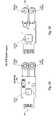
- FIG. 1is a high level schematic of an exemplary embodiment of an 8 G SFP module having a 4 G SFP architecture
- FIG. 2Ais a view of a first side of an exemplary 8 G SFP board showing the arrangement of a ROSA, TOSA, EEPROM and FCC;
- FIG. 2Bis a view of a second side of an exemplary 8 G SFP board showing the arrangement of the ROSA, TOSA, and an LDPA;
- FIG. 3indicates electrical and optical eye diagrams corresponding to operation of an exemplary embodiment of the 8 G SFP transceiver at about a 2.5 Gb/s data rate;
- FIG. 4indicates electrical and optical eye diagrams corresponding to operation an exemplary embodiment of the 8 G SFP transceiver at about a 4.25 Gb/s data rate
- FIG. 5indicates electrical and optical eye diagrams corresponding to operation of an exemplary embodiment of the 8 G SFP transceiver at about a 8.5 Gb/s data rate.
- Exemplary embodiments of the inventionare concerned with an 2/4/8 Gb/s (“8 G”) SFP transceiver that substantially comprises a 4 G SFP architecture.
- 8 G2/4/8 Gb/s
- nominal rates of 8 Gare achieved within a desired SFP MSA form factor while meeting performance standards, and without necessitating CDR data signal integrity compensation.
- 8 G nominal data ratesare achieved with the 4 G SFP architecture. Such data rates may be achieved in this way for various protocols, one example of which is Fibre Channel. Note that the aforementioned 8 G nominal data rate is approximately 8.5 G in the Fibre Channel protocol, and may take other values in connection with other protocols. Accordingly, the scope of the invention is not limited simply to 8 Gb/s and 8.5 Gb/s data rates. In addition to supporting the nominal 8 G data rate, at least some embodiments of the invention are also backwards compatible with nominal 1/2/4 G data rates for protocols which include Fibre Channel. This is particularly useful since the transceiver can thus operate in connection with 1/2/4 G legacy systems.
- exemplary embodiments of the inventionare able to achieve relatively high data rates, with acceptable performance, without requiring data signal integrity compensation. Elimination of data signal integrity compensation circuits and devices enables relatively low power dissipation to be achieved. In general, power dissipations in the region of about ⁇ 1 W can be achieved. In some short wave applications, power dissipation is only about ⁇ 600 mW, and in some long wave applications, power dissipation is only about ⁇ 800 mW.
- an exemplary SFP transceiverAs noted above, one exemplary embodiment of the invention is concerned with a Fibre Channel compatible transceiver that is generally implemented in the form of a 4 G SFP transceiver, such as is employed in Fibre Channel and Ethernet applications. Because the transceiver is generally compliant with the SFP MSA, incorporated herein in its entirety by this reference, no data signal integrity compensation methods or circuitry are implemented in the exemplary transceiver and, as the disclosure herein indicates, no such data signal integrity compensation is necessary to achieve data rates such as 8.5 Gb/s.
- exemplary transceiversthat do not require or implement CDR, or comparable, functionality may be referred to herein as comprising or implementing “uncompensated” data signal generation and/or processing components and circuitry. More generally, such transceivers may be referred to as comprising or embodying an “uncompensated” architecture. In similar fashion, operation of such exemplary transceivers may be referred to generally herein as “uncompensated” operation.
- At least some embodiments of the inventioncomprise a 2/4/8 G SFP transceiver without CDR. Other embodiments are directed to a 4/8 G SFP transceiver without CDR. More generally, embodiments of the invention are concerned with SFP transceivers that are able to support some or all of the 1/2/4/8 G nominal data rates, although such transceivers may generally be referred to herein as an “8 G SFP transceiver.”
- exemplary embodiments of the inventionhave the same port density as 1/2/4 G Fibre Channel and have an optical backward compatibility with 2/4 G Fibre Channel. Additionally, embodiments of the invention are electrically and mechanically backward compatible with 2/4 G Fibre Channel, that is, the electrical connector and cage of the transceiver are configured to interface with 2/4 G Fibre Channel systems and components.
- an exemplary embodiment of the 8 G SFP transceivercan be employed in connection with 2/4 G legacy systems, and legacy 2/4 G modules can be used in 8 G systems.
- the 8 G SFP transceivermay be adjusted or modified. As one example, if backward compatibility of the 8 G SFP transceiver is only needed for 2/4 G Fibre Channel, bandwidth tunability of the receiver may not be required. Correspondingly, some embodiments of the invention employ a receiver with a sensitivity of ⁇ 19 dBm at 10.7 G. The receiver may or may not be a fixed bandwidth receiver.
- Sample receiver sensitivity specificationsinclude: ⁇ 20 dBm (FTRJ8524) at 1.0626 G; ⁇ 18 dBm (FTRJ8524) at 2.125 G; and, ⁇ 15 dBm (FTRJ8524) at 4.25 G.
- One exemplary embodiment of the inventionhas a measured receiver sensitivity of ⁇ 20 dBm (FTRJ8524) at 4.25 G.
- Another embodiment of the inventionusing the exemplary HFD6x80-41 ROSA and Vitesse post amplifier discussed below, has a measured receiver sensitivity of ⁇ 16 dBm (FTRJ8524) at 8.5 G, with an extinction ratio (“ER”) of 3-4 dB and 10 ⁇ 10 .
- FIG. 1is a block diagram illustrating aspects of an exemplary transceiver module 100
- FIG. 2is a photograph of an 8 G board 102 that conforms to the SFP MSA.
- the illustrated transceiver 100includes an integrated LDPA 101 configured for communication with a TOSA 103 and a ROSA 105 , where the ROSA 103 and TOSA 105 are nominally rated for 10 Gb/s operation.
- LDPA 101is a 4 G laser driver-post amplifier such as those produced by Vitesse Semiconductor Corporation (“Vitesse”).
- VitesseVitesse Semiconductor Corporation
- One particular Vitesse model that may be usedis the Vitesse VSC7964 laser driver and limiting amplifier.
- other LDPAs of comparable functionality and configurationmay alternatively be employed.
- Separate laser drivers and post-amplifiersmay also be used in some embodiments of the invention.
- the TOSA 103 and ROSA 105are exemplified by optoelectronic devices produced by Advanced Optical Components (“ADOPCO”) of Richardson, Tex.
- the TOSA 103may comprise, for example, an ADOPCO HFE6x9x-56 TOSA with an 850 nm vertical cavity surface emitting laser (“VCSEL”) and having an associated nominal data rate of 10 G.
- the ROSA 105may comprise, for example, an ADOPCO HFD6x80-41 ROSA with 850 nm P-I-N detector and preamp, and having an associated nominal data rate of 10 G.
- the ROSA 105 and TOSA 103are hard-connected to the circuit board 102 of the transceiver 100 . In alternative embodiments however, the ROSA and/or TOSA employ flex connections.
- ROSA and/or TOSAof comparable functionality, performance, and configuration may alternatively be employed however.
- a ROSA and/or TOSA having a nominal data rate greater or less than 10 Gmay be employed in some cases.
- embodiments of the inventionare not limited to 850 nm devices, and devices operating at other wavelengths may also be employed.
- optical transmitters other than VCSELsmay be employed. Examples of alternative optical transmitters include distributed feedback (“DFB”) lasers and Fabry-Perot (“FP”) lasers.
- DFBdistributed feedback
- FPFabry-Perot
- the exemplary 8 G SFP transceiver 100further includes digital diagnostics systems and functionality, implemented in part by a diagnostics control chip (“DCC”) 104 that interfaces with both internal and external devices.
- DCCdiagnostics control chip
- One suitable diagnostics control chipis an Atmel SL828 microcontroller, although other devices of comparable functionality and configuration may alternatively be employed.
- the exemplary 8 G SFP transceiver 100is configured so that the DCC 104 and the LDPA 101 are located on opposing sides of the transceiver circuit board so as to facilitate efficient use of the space in the transceiver housing.
- the illustrated embodimentfurther includes, among other things, an EEPROM 106 .
- aspects of embodiments of the inventionmay be modified as necessary to achieve the nominal 8 G rate in an SFP form factor.
- the lengths of one or more traces of the transceiver boardmay be minimized to the extent that the exemplary implementation will permit, so as to enhance performance.
- fixed electrical equalization and preemphasismay be implemented in the transceiver if particular traces, such as FR4 traces for example, exceed a certain length, such as about 2 to about 3 inches for example.
- Suitable trace lengthsmay vary from one embodiment to another but can be readily determined in various ways, such as through the use of a module demonstrator for example.
- Exemplary embodiments of the 8 G SFP transceiverare well suited for use in connection with the Fibre Channel protocol. However, the scope of the invention is not limited to any particular protocol.
- the 8 G SFP transceivercan be used as a short wave solution for 100 m multimode fiber (“MMF”) (50 ⁇ m 500 MHz km).
- MMFmultimode fiber
- the 8 G SFP transceivercan be used as a short wave solution for distances up to at least about 10 km using single mode fiber (“SMF”).
- SMFsingle mode fiber
- embodiments of the inventionmay take various forms. For example, 100 m short wave applications are suitable for employing an 850 nm VCSEL. Longer link lengths, such as 1-2 km long transceiver other than the optical emitter may additionally or alternatively be modified if necessary.
- FIGS. 3 through 5indicate that both optical and electrical masks are maintained at the following data rates: 2.5 G (Rx sensitivity of ⁇ 19 dBm); 4.25 G (Rx sensitivity ⁇ 19 dBm); and, 8.5 G (Rx sensitivity ⁇ 16 dBm).
- the distortion in the upper portion of the optical eye diagramis due to a bad connector, and does not reflect any shortcoming in the construction, arrangement or performance of the associated transceiver.
- embodiments of the inventionare able to employ a 4 G SFP architecture to successfully operate at relatively high data rates, such as 8.5 Gb/s or higher, without CDR or comparable compensation, while maintaining compliance with operational standards and requirements such as masks and eye diagram requirements.
Landscapes
- Physics & Mathematics (AREA)
- Electromagnetism (AREA)
- Engineering & Computer Science (AREA)
- Computer Networks & Wireless Communication (AREA)
- Signal Processing (AREA)
- General Physics & Mathematics (AREA)
- Optics & Photonics (AREA)
- Optical Couplings Of Light Guides (AREA)
- Optical Communication System (AREA)
Abstract
Description
Claims (18)
Priority Applications (8)
| Application Number | Priority Date | Filing Date | Title |
|---|---|---|---|
| US11/074,609US7970283B2 (en) | 2005-03-07 | 2005-03-07 | High speed SFP transceiver |
| TW095106635ATW200637197A (en) | 2005-03-07 | 2006-02-27 | High speed SFP transceiver |
| EP06737366AEP1856823A2 (en) | 2005-03-07 | 2006-03-06 | High speed sfp transceiver |
| JP2008500861AJP2008533825A (en) | 2005-03-07 | 2006-03-06 | High-speed SEP transceiver |
| AU2006220618AAU2006220618A1 (en) | 2005-03-07 | 2006-03-06 | High speed SFP transceiver |
| KR1020077022032AKR20070120114A (en) | 2005-03-07 | 2006-03-06 | High Speed SPF Transceiver |
| CNA2006800075533ACN101138176A (en) | 2005-03-07 | 2006-03-06 | High speed sfp transceiver |
| PCT/US2006/008187WO2006096751A2 (en) | 2005-03-07 | 2006-03-06 | High speed sfp transceiver |
Applications Claiming Priority (1)
| Application Number | Priority Date | Filing Date | Title |
|---|---|---|---|
| US11/074,609US7970283B2 (en) | 2005-03-07 | 2005-03-07 | High speed SFP transceiver |
Publications (2)
| Publication Number | Publication Date |
|---|---|
| US20060198639A1 US20060198639A1 (en) | 2006-09-07 |
| US7970283B2true US7970283B2 (en) | 2011-06-28 |
Family
ID=36944224
Family Applications (1)
| Application Number | Title | Priority Date | Filing Date |
|---|---|---|---|
| US11/074,609Active2026-01-20US7970283B2 (en) | 2005-03-07 | 2005-03-07 | High speed SFP transceiver |
Country Status (8)
| Country | Link |
|---|---|
| US (1) | US7970283B2 (en) |
| EP (1) | EP1856823A2 (en) |
| JP (1) | JP2008533825A (en) |
| KR (1) | KR20070120114A (en) |
| CN (1) | CN101138176A (en) |
| AU (1) | AU2006220618A1 (en) |
| TW (1) | TW200637197A (en) |
| WO (1) | WO2006096751A2 (en) |
Cited By (7)
| Publication number | Priority date | Publication date | Assignee | Title |
|---|---|---|---|---|
| US20120195601A1 (en)* | 2011-01-27 | 2012-08-02 | Avago Technologies Fiber Ip (Singapore) Pte. Ltd. | Optical transmitter with hybridly integrated driver |
| US9038141B2 (en) | 2011-12-07 | 2015-05-19 | Adc Telecommunications, Inc. | Systems and methods for using active optical cable segments |
| US9207417B2 (en) | 2012-06-25 | 2015-12-08 | Adc Telecommunications, Inc. | Physical layer management for an active optical module |
| US9380874B2 (en) | 2012-07-11 | 2016-07-05 | Commscope Technologies Llc | Cable including a secure physical layer management (PLM) whereby an aggregation point can be associated with a plurality of inputs |
| US9473361B2 (en) | 2012-07-11 | 2016-10-18 | Commscope Technologies Llc | Physical layer management at a wall plate device |
| US9544058B2 (en) | 2013-09-24 | 2017-01-10 | Commscope Technologies Llc | Pluggable active optical module with managed connectivity support and simulated memory table |
| US9933984B1 (en)* | 2014-09-29 | 2018-04-03 | Advanced Testing Technologies, Inc. | Method and arrangement for eye diagram display of errors of digital waveforms |
Families Citing this family (10)
| Publication number | Priority date | Publication date | Assignee | Title |
|---|---|---|---|---|
| US8296117B2 (en)* | 2008-01-31 | 2012-10-23 | Ca, Inc. | Business process optimizer |
| US8175991B2 (en)* | 2008-01-31 | 2012-05-08 | Ca, Inc. | Business optimization engine that extracts process life cycle information in real time by inserting stubs into business applications |
| US20090198533A1 (en)* | 2008-01-31 | 2009-08-06 | Computer Associates Think, Inc. | Business process extractor |
| WO2010068596A1 (en) | 2008-12-11 | 2010-06-17 | Pulse Engineering, Inc. | Connector shielding apparatus and methods |
| GB2477104B (en)* | 2010-01-21 | 2017-02-22 | Ge Oil & Gas Uk Ltd | Communications connection in a subsea well |
| CN101958755A (en)* | 2010-10-25 | 2011-01-26 | 江苏飞格光电有限公司 | SFP (Small Form-factor Pluggable) miniaturized photoelectric receiving-transmitting module |
| CN102801967B (en)* | 2012-07-10 | 2017-02-08 | 深圳市易飞扬通信技术有限公司 | SFP (System File Protection) optical module for transferring non-compressed video signal |
| CN103138839B (en)* | 2013-02-22 | 2015-05-13 | 烽火通信科技股份有限公司 | Hardware implementation system compatible with multi-rate fiber channel services |
| CN114531185B (en)* | 2022-02-11 | 2023-06-16 | 南京邮电大学 | Transceiver joint design method based on symbol-level information |
| US20240068905A1 (en)* | 2022-08-25 | 2024-02-29 | Ii-Vi Delaware, Inc. | Pluggable Optical Time Domain Reflectometer |
Citations (12)
| Publication number | Priority date | Publication date | Assignee | Title |
|---|---|---|---|---|
| US6272154B1 (en)* | 1998-10-30 | 2001-08-07 | Tellium Inc. | Reconfigurable multiwavelength network elements |
| JP2002051010A (en) | 2000-06-02 | 2002-02-15 | Trw Inc | Optical electronic communication system provided with photo detector array and time compensation in turbulence medium |
| US20020149821A1 (en)* | 2001-02-05 | 2002-10-17 | Aronson Lewis B. | Integrated memory mapped controller circuit for fiber optics transceiver |
| US20030002108A1 (en)* | 2001-06-27 | 2003-01-02 | International Business Machines Corporation | Detection of data transmission rates using passing frequency-selective filtering |
| WO2004002023A2 (en)* | 2002-06-25 | 2003-12-31 | Finisar Corporation | Transceiver module and integrated circuit with dual eye openers |
| US20040022544A1 (en)* | 2002-08-02 | 2004-02-05 | Dan Case | Transceiver with programmable signal parameters |
| GB2397408A (en) | 2003-01-15 | 2004-07-21 | Agilent Technologies Inc | EEPROM emulation in an optical transceiver |
| TW200425588A (en) | 2003-05-08 | 2004-11-16 | Hon Hai Prec Ind Co Ltd | SFP transceiver |
| US20050003696A1 (en) | 2002-12-04 | 2005-01-06 | Tyco Electronics Corporation | Lever style de-latch mechanism for pluggable electronic module |
| WO2005015798A1 (en) | 2003-08-07 | 2005-02-17 | Pirelli & C. S.P.A. | A modular, easily configurable and expandible node structure for an optical communications network |
| JP2005535271A (en) | 2002-08-02 | 2005-11-17 | フィニサー コーポレイション | Transceiver with programmable signal parameters |
| US7156562B2 (en)* | 2003-07-15 | 2007-01-02 | National Semiconductor Corporation | Opto-electronic module form factor having adjustable optical plane height |
- 2005
- 2005-03-07USUS11/074,609patent/US7970283B2/enactiveActive
- 2006
- 2006-02-27TWTW095106635Apatent/TW200637197A/enunknown
- 2006-03-06AUAU2006220618Apatent/AU2006220618A1/ennot_activeAbandoned
- 2006-03-06EPEP06737366Apatent/EP1856823A2/ennot_activeWithdrawn
- 2006-03-06JPJP2008500861Apatent/JP2008533825A/enactivePending
- 2006-03-06CNCNA2006800075533Apatent/CN101138176A/enactivePending
- 2006-03-06WOPCT/US2006/008187patent/WO2006096751A2/enactiveApplication Filing
- 2006-03-06KRKR1020077022032Apatent/KR20070120114A/ennot_activeCeased
Patent Citations (12)
| Publication number | Priority date | Publication date | Assignee | Title |
|---|---|---|---|---|
| US6272154B1 (en)* | 1998-10-30 | 2001-08-07 | Tellium Inc. | Reconfigurable multiwavelength network elements |
| JP2002051010A (en) | 2000-06-02 | 2002-02-15 | Trw Inc | Optical electronic communication system provided with photo detector array and time compensation in turbulence medium |
| US20020149821A1 (en)* | 2001-02-05 | 2002-10-17 | Aronson Lewis B. | Integrated memory mapped controller circuit for fiber optics transceiver |
| US20030002108A1 (en)* | 2001-06-27 | 2003-01-02 | International Business Machines Corporation | Detection of data transmission rates using passing frequency-selective filtering |
| WO2004002023A2 (en)* | 2002-06-25 | 2003-12-31 | Finisar Corporation | Transceiver module and integrated circuit with dual eye openers |
| US20040022544A1 (en)* | 2002-08-02 | 2004-02-05 | Dan Case | Transceiver with programmable signal parameters |
| JP2005535271A (en) | 2002-08-02 | 2005-11-17 | フィニサー コーポレイション | Transceiver with programmable signal parameters |
| US20050003696A1 (en) | 2002-12-04 | 2005-01-06 | Tyco Electronics Corporation | Lever style de-latch mechanism for pluggable electronic module |
| GB2397408A (en) | 2003-01-15 | 2004-07-21 | Agilent Technologies Inc | EEPROM emulation in an optical transceiver |
| TW200425588A (en) | 2003-05-08 | 2004-11-16 | Hon Hai Prec Ind Co Ltd | SFP transceiver |
| US7156562B2 (en)* | 2003-07-15 | 2007-01-02 | National Semiconductor Corporation | Opto-electronic module form factor having adjustable optical plane height |
| WO2005015798A1 (en) | 2003-08-07 | 2005-02-17 | Pirelli & C. S.P.A. | A modular, easily configurable and expandible node structure for an optical communications network |
Non-Patent Citations (10)
| Title |
|---|
| Abe et al: "Short Wave SFF Small Form Factor Transceivers", IEEE, 2001 Electronic Components and Technology Conference, May 29, 2001-Jun. 1, 2001, pp. 1-5.* |
| Abe,S., "Short Wave SFF Small Form Factor Transceivers", 2001 Electronic Components and Technology Conference. |
| Gomatam et al: "Performance Study of 8.5G Links", Oct. 13, 2004, ftp://ftp.t10.org/t11/document.04/04-661v1.pdf, pp. 1-13, and documents showing the publication date.* |
| Gomatam et al: "Performance Study of 8.5G Links", Oct. 13, 2004, ftp://ftp.t10.org/t11/document.04/04-661v1.pdf, pp. 1-13.* |
| Hashimoto et al: "A Bidirectional Single Fiber 1.25 Gb/s Optical Transceiver Module with SFP Package Using PLC", 2003 Electronic Components and Technology Conference, p. 279-283.* |
| Infeineon Technologies: "SPF-Small Form-factor Pluggable Multimode 850 nm 2.125 and 1.0625 Gbit/s Fiber Channel 1.25 Gigabit Ethernet Transceiver with LCTM Connector", Apr. 25, 2003, http://www.datasheetcatalog.org/datasheet/infineon/1-V23818-M305-B57-030425-1440.pdf, pp. 1-20.* |
| Priyadarshi et al: "The First Hot Pluggable 2.5 Gb/s DWDM Transceiver in an SFP Form Factor", IEEE Optical Communications, Feb. 2005, p. S29-S31.* |
| Priyadarshi, S. et al., "The First Hot Pluggable 2.5 Gb/s DWDM Transceiver in an SFP Form Factor", IEEE Optical Communications, Feb. 2005, pp. 529-531. |
| Vitesse: "Performance Study of 8.5G Links", Oct. 13, 2004.* |
| Vitesse: "SFP Pro Chipset and Reference Design", Oct. 2004.* |
Cited By (13)
| Publication number | Priority date | Publication date | Assignee | Title |
|---|---|---|---|---|
| US8611755B2 (en)* | 2011-01-27 | 2013-12-17 | Avago Technologies General Ip (Singapore) Pte. Ltd. | Optical transmitter with hybridly integrated driver |
| US20120195601A1 (en)* | 2011-01-27 | 2012-08-02 | Avago Technologies Fiber Ip (Singapore) Pte. Ltd. | Optical transmitter with hybridly integrated driver |
| USRE47365E1 (en) | 2011-12-07 | 2019-04-23 | Commscope Technologies Llc | Systems and methods for using active optical cable segments |
| US9038141B2 (en) | 2011-12-07 | 2015-05-19 | Adc Telecommunications, Inc. | Systems and methods for using active optical cable segments |
| US9207417B2 (en) | 2012-06-25 | 2015-12-08 | Adc Telecommunications, Inc. | Physical layer management for an active optical module |
| US9602897B2 (en) | 2012-06-25 | 2017-03-21 | Commscope Technologies Llc | Physical layer management for an active optical module |
| US9380874B2 (en) | 2012-07-11 | 2016-07-05 | Commscope Technologies Llc | Cable including a secure physical layer management (PLM) whereby an aggregation point can be associated with a plurality of inputs |
| US9473361B2 (en) | 2012-07-11 | 2016-10-18 | Commscope Technologies Llc | Physical layer management at a wall plate device |
| US9742704B2 (en) | 2012-07-11 | 2017-08-22 | Commscope Technologies Llc | Physical layer management at a wall plate device |
| US9544058B2 (en) | 2013-09-24 | 2017-01-10 | Commscope Technologies Llc | Pluggable active optical module with managed connectivity support and simulated memory table |
| US10205519B2 (en) | 2013-09-24 | 2019-02-12 | Commscope Technologies Llc | Pluggable active optical module with managed connectivity support and simulated memory table |
| US10700778B2 (en) | 2013-09-24 | 2020-06-30 | Commscope Technologies Llc | Pluggable active optical module with managed connectivity support and simulated memory table |
| US9933984B1 (en)* | 2014-09-29 | 2018-04-03 | Advanced Testing Technologies, Inc. | Method and arrangement for eye diagram display of errors of digital waveforms |
Also Published As
| Publication number | Publication date |
|---|---|
| CN101138176A (en) | 2008-03-05 |
| US20060198639A1 (en) | 2006-09-07 |
| WO2006096751A3 (en) | 2007-04-26 |
| KR20070120114A (en) | 2007-12-21 |
| TW200637197A (en) | 2006-10-16 |
| WO2006096751A2 (en) | 2006-09-14 |
| JP2008533825A (en) | 2008-08-21 |
| EP1856823A2 (en) | 2007-11-21 |
| AU2006220618A1 (en) | 2006-09-14 |
Similar Documents
| Publication | Publication Date | Title |
|---|---|---|
| AU2006220618A1 (en) | High speed SFP transceiver | |
| US6665498B1 (en) | High-speed optical data links | |
| US7380993B2 (en) | Optical transceiver for 100 gigabit/second transmission | |
| US9172473B2 (en) | Active linear amplifier inside transmitter module | |
| US20080292322A1 (en) | Optoelectronic devices with intelligent transmitter modules | |
| US6951426B2 (en) | Pad architecture for backwards compatibility for bi-directional transceiver module | |
| US8135281B2 (en) | Free space optical connector | |
| US20040264879A1 (en) | Optical cable with integrated electrical connector | |
| JP2016201790A (en) | Two-way free-space laser communication system for Gigabit Ethernet telemetry data | |
| CN102116914A (en) | Miniaturized double-path optical module | |
| US7481656B2 (en) | Optical transceiver PCB mounting system having EMI containment features | |
| US9497525B2 (en) | Optical engines and optical cable assemblies having electrical signal conditioning | |
| US20240223349A1 (en) | Communication device, communication system, and optical module | |
| US7580434B2 (en) | Dual laser driver architecture in an optical transceiver | |
| KR20080080341A (en) | System and method and optical transceiver for increasing optical link distance | |
| Tsunoda et al. | 24 to 34-Gb/s× 4 multi-rate VCSEL-based optical transceiver with referenceless CDR | |
| Tsunoda et al. | 25.78-Gb/s VCSEL-based optical transceiver with retimer-embedded driver and receiver ICs | |
| CN115664527A (en) | Optical module and optical communication system | |
| CN201974550U (en) | Miniaturized double-channel optical module | |
| EP1417786A1 (en) | High-speed optical data links | |
| EP1357682A1 (en) | Module apparatus for optical communication and circuit pack therefor | |
| Wang et al. | Power Efficient Parallel Optical Communication Links | |
| CDRs et al. | optical | |
| JPH05130040A (en) | Optical transmitter-receiver |
Legal Events
| Date | Code | Title | Description |
|---|---|---|---|
| AS | Assignment | Owner name:FINISAR CORPORATION, CALIFORNIA Free format text:ASSIGNMENT OF ASSIGNORS INTEREST;ASSIGNORS:GIARETTA, GIORGIO;ENG, JULIE SHERIDAN;MCVEY, THOMAS GORDON BECK;REEL/FRAME:016014/0016;SIGNING DATES FROM 20050314 TO 20050315 | |
| AS | Assignment | Owner name:FINISAR CORPORATION, CALIFORNIA Free format text:CORRECTIVE ASSIGNMENT TO CORRECT THE LAST NAME OF THIRD ASSIGNOR PREVIOUSLY RECORDED ON REEL 016014 FRAME 0016;ASSIGNORS:GIARETTA, GIORGIO;ENG, JULIE SHERIDAN;MASON, THOMAS GORDON BECK;REEL/FRAME:016276/0981;SIGNING DATES FROM 20050314 TO 20050315 | |
| STCF | Information on status: patent grant | Free format text:PATENTED CASE | |
| CC | Certificate of correction | ||
| FPAY | Fee payment | Year of fee payment:4 | |
| MAFP | Maintenance fee payment | Free format text:PAYMENT OF MAINTENANCE FEE, 8TH YEAR, LARGE ENTITY (ORIGINAL EVENT CODE: M1552); ENTITY STATUS OF PATENT OWNER: LARGE ENTITY Year of fee payment:8 | |
| AS | Assignment | Owner name:BANK OF AMERICA, N.A., AS ADMINISTRATIVE AGENT, NO Free format text:NOTICE OF GRANT OF SECURITY INTEREST IN PATENTS;ASSIGNORS:II-VI INCORPORATED;MARLOW INDUSTRIES, INC.;EPIWORKS, INC.;AND OTHERS;REEL/FRAME:050484/0204 Effective date:20190924 Owner name:BANK OF AMERICA, N.A., AS ADMINISTRATIVE AGENT, NORTH CAROLINA Free format text:NOTICE OF GRANT OF SECURITY INTEREST IN PATENTS;ASSIGNORS:II-VI INCORPORATED;MARLOW INDUSTRIES, INC.;EPIWORKS, INC.;AND OTHERS;REEL/FRAME:050484/0204 Effective date:20190924 | |
| AS | Assignment | Owner name:II-VI DELAWARE, INC., DELAWARE Free format text:ASSIGNMENT OF ASSIGNORS INTEREST;ASSIGNOR:FINISAR CORPORATION;REEL/FRAME:052286/0001 Effective date:20190924 | |
| AS | Assignment | Owner name:JPMORGAN CHASE BANK, N.A., AS COLLATERAL AGENT, NEW YORK Free format text:SECURITY INTEREST;ASSIGNORS:II-VI INCORPORATED;II-VI DELAWARE, INC.;M CUBED TECHNOLOGIES, INC.;AND OTHERS;REEL/FRAME:060562/0254 Effective date:20220701 | |
| AS | Assignment | Owner name:PHOTOP TECHNOLOGIES, INC., CALIFORNIA Free format text:PATENT RELEASE AND REASSIGNMENT;ASSIGNOR:BANK OF AMERICA, N.A., AS ADMINISTRATIVE AGENT;REEL/FRAME:060574/0001 Effective date:20220701 Owner name:II-VI OPTOELECTRONIC DEVICES, INC., NEW JERSEY Free format text:PATENT RELEASE AND REASSIGNMENT;ASSIGNOR:BANK OF AMERICA, N.A., AS ADMINISTRATIVE AGENT;REEL/FRAME:060574/0001 Effective date:20220701 Owner name:II-VI DELAWARE, INC., PENNSYLVANIA Free format text:PATENT RELEASE AND REASSIGNMENT;ASSIGNOR:BANK OF AMERICA, N.A., AS ADMINISTRATIVE AGENT;REEL/FRAME:060574/0001 Effective date:20220701 Owner name:II-VI PHOTONICS (US), INC., MASSACHUSETTS Free format text:PATENT RELEASE AND REASSIGNMENT;ASSIGNOR:BANK OF AMERICA, N.A., AS ADMINISTRATIVE AGENT;REEL/FRAME:060574/0001 Effective date:20220701 Owner name:M CUBED TECHNOLOGIES, INC., CONNECTICUT Free format text:PATENT RELEASE AND REASSIGNMENT;ASSIGNOR:BANK OF AMERICA, N.A., AS ADMINISTRATIVE AGENT;REEL/FRAME:060574/0001 Effective date:20220701 Owner name:II-VI OPTICAL SYSTEMS, INC., CALIFORNIA Free format text:PATENT RELEASE AND REASSIGNMENT;ASSIGNOR:BANK OF AMERICA, N.A., AS ADMINISTRATIVE AGENT;REEL/FRAME:060574/0001 Effective date:20220701 Owner name:FINISAR CORPORATION, CALIFORNIA Free format text:PATENT RELEASE AND REASSIGNMENT;ASSIGNOR:BANK OF AMERICA, N.A., AS ADMINISTRATIVE AGENT;REEL/FRAME:060574/0001 Effective date:20220701 Owner name:OPTIUM CORPORATION, CALIFORNIA Free format text:PATENT RELEASE AND REASSIGNMENT;ASSIGNOR:BANK OF AMERICA, N.A., AS ADMINISTRATIVE AGENT;REEL/FRAME:060574/0001 Effective date:20220701 Owner name:COADNA PHOTONICS, INC., PENNSYLVANIA Free format text:PATENT RELEASE AND REASSIGNMENT;ASSIGNOR:BANK OF AMERICA, N.A., AS ADMINISTRATIVE AGENT;REEL/FRAME:060574/0001 Effective date:20220701 Owner name:KAILIGHT PHOTONICS, INC., CALIFORNIA Free format text:PATENT RELEASE AND REASSIGNMENT;ASSIGNOR:BANK OF AMERICA, N.A., AS ADMINISTRATIVE AGENT;REEL/FRAME:060574/0001 Effective date:20220701 Owner name:LIGHTSMYTH TECHNOLOGIES, INC., OREGON Free format text:PATENT RELEASE AND REASSIGNMENT;ASSIGNOR:BANK OF AMERICA, N.A., AS ADMINISTRATIVE AGENT;REEL/FRAME:060574/0001 Effective date:20220701 Owner name:EPIWORKS, INC., ILLINOIS Free format text:PATENT RELEASE AND REASSIGNMENT;ASSIGNOR:BANK OF AMERICA, N.A., AS ADMINISTRATIVE AGENT;REEL/FRAME:060574/0001 Effective date:20220701 Owner name:MARLOW INDUSTRIES, INC., TEXAS Free format text:PATENT RELEASE AND REASSIGNMENT;ASSIGNOR:BANK OF AMERICA, N.A., AS ADMINISTRATIVE AGENT;REEL/FRAME:060574/0001 Effective date:20220701 Owner name:II-VI INCORPORATED, PENNSYLVANIA Free format text:PATENT RELEASE AND REASSIGNMENT;ASSIGNOR:BANK OF AMERICA, N.A., AS ADMINISTRATIVE AGENT;REEL/FRAME:060574/0001 Effective date:20220701 | |
| MAFP | Maintenance fee payment | Free format text:PAYMENT OF MAINTENANCE FEE, 12TH YEAR, LARGE ENTITY (ORIGINAL EVENT CODE: M1553); ENTITY STATUS OF PATENT OWNER: LARGE ENTITY Year of fee payment:12 |