US7969235B2 - Self-adaptive multi-stage charge pump - Google Patents
Self-adaptive multi-stage charge pumpDownload PDFInfo
- Publication number
- US7969235B2 US7969235B2US12/570,646US57064609AUS7969235B2US 7969235 B2US7969235 B2US 7969235B2US 57064609 AUS57064609 AUS 57064609AUS 7969235 B2US7969235 B2US 7969235B2
- Authority
- US
- United States
- Prior art keywords
- output
- stages
- charge pump
- gate
- generation
- Prior art date
- Legal status (The legal status is an assumption and is not a legal conclusion. Google has not performed a legal analysis and makes no representation as to the accuracy of the status listed.)
- Expired - Fee Related
Links
Images


Classifications
- H—ELECTRICITY
- H02—GENERATION; CONVERSION OR DISTRIBUTION OF ELECTRIC POWER
- H02M—APPARATUS FOR CONVERSION BETWEEN AC AND AC, BETWEEN AC AND DC, OR BETWEEN DC AND DC, AND FOR USE WITH MAINS OR SIMILAR POWER SUPPLY SYSTEMS; CONVERSION OF DC OR AC INPUT POWER INTO SURGE OUTPUT POWER; CONTROL OR REGULATION THEREOF
- H02M3/00—Conversion of DC power input into DC power output
- H02M3/02—Conversion of DC power input into DC power output without intermediate conversion into AC
- H02M3/04—Conversion of DC power input into DC power output without intermediate conversion into AC by static converters
- H02M3/06—Conversion of DC power input into DC power output without intermediate conversion into AC by static converters using resistors or capacitors, e.g. potential divider
- H02M3/07—Conversion of DC power input into DC power output without intermediate conversion into AC by static converters using resistors or capacitors, e.g. potential divider using capacitors charged and discharged alternately by semiconductor devices with control electrode, e.g. charge pumps
- H02M3/073—Charge pumps of the Schenkel-type
Definitions
- This inventionpertains generally to the field of charge pumps and more particularly to multi-stage charge pumps where the number of stages self-adjusts.
- Charge pumpsuse a switching process to provide a DC output voltage larger or lower than its DC input voltage.
- a charge pumpwill have a capacitor coupled to switches between an input and an output.
- the charging half cyclethe capacitor couples in parallel to the input so as to charge up to the input voltage.
- the transfer half cyclethe charged capacitor couples in series with the input voltage so as to provide an output voltage twice the level of the input voltage.
- FIGS. 1 a and 1 bThis process is illustrated in FIGS. 1 a and 1 b .
- the capacitor 5is arranged in parallel with the input voltage V IN to illustrate the charging half cycle.
- the charged capacitor 5is arranged in series with the input voltage to illustrate the transfer half cycle.
- the positive terminal of the charged capacitor 5will thus be 2*V IN with respect to ground.
- Charge pumpsare used in many contexts. For example, they are used as peripheral circuits on flash and other non-volatile memories to generate many of the needed operating voltages, such as programming or erase voltages, from a lower power supply voltage.
- a number of charge pump designs, such as conventional Dickson-type pumps,are know in the art. But given the common reliance upon charge pumps, there is an on going need for improvements in pump design, particularly with respect to trying to reduce the amount of layout area and the efficiency of pumps.
- a charge pump circuit for generating an output voltageincludes N output generation stages, where N is an integer greater than one, each of which has a first branch receiving a first clock signal and providing a first output and a second branch receiving a second clock signal and providing a second output.
- the first and second clock signalsare non-overlapping.
- the charge pump circuitalso includes N corresponding gate stages, each having a first branch receiving the first clock signal and providing a first output and a second branch receiving the second clock signal and providing a second output, wherein the output generation stages and the corresponding gate stages have the same structure.
- the charge pump circuitfurther includes N corresponding first transistors and N corresponding second transistors.
- the output generation stagesare connected in series with the first and second output of each of the output generation stages except the last in the series respectively connected through the corresponding first and second transistors to provide the input for the next output generation stage, the first and second outputs of the last in the series of output generation stages respectively connected through the corresponding first and second transistors to provide the output voltage of the charge pump.
- the gate stagesare connected in series with the first and second output of each of the gate stages except the last in the series connected through a corresponding diode to provide the input for the next gate stage, and the first and second outputs of each of the gate stages respectively connected to the control gate the correspond first and second transistors.
- a charge pump system circuit for generating an outputincludes N output generation stages and corresponding N gate stages, wherein the output generation stages and the corresponding gate stages have the same structure and N is an integer greater than one.
- the charge pump systemfurther includes N corresponding switches.
- the output generation stagesare connected in series with an output of each of the output generation stages except the last in the series being connected through the corresponding switch to provide an input for the next output generation stage, the output of the last in the series of output being connected through the corresponding switch to provide the output of the charge pump.
- the gate stagesare connected in series with an output of each of the gate stages respectively connected to the control the correspond switch.
- the charge pump systemalso includes regulation circuitry connected to receive the output of the charge pump and to regulate the operation of the output generation stages based upon said output of the charge pump, whereby the number of output generation stages active in boosting the output is automatically adjusted.
- FIG. 1 ais a simplified circuit diagram of the charging half cycle in a generic charge pump.
- FIG. 1 bis a simplified circuit diagram of the transfer half cycle in a generic charge pump.
- FIG. 2is a top-level block diagram for a regulated charge pump.
- FIGS. 3A and 3Bshow a 2 stage, 2 branch version of a conventional Dickson type charge pump and corresponding clock signals.
- FIGS. 4A and 4Bshow an exemplary embodiment based on a voltage doubler-type of charge pump.
- FIG. 5shows a comparison of the output I-V curve for the exemplary embodiment versus a conventional pump design.
- FIG. 6shows a comparison of the output (Iout/Iin) versus Vout curve for the exemplary embodiment versus a conventional pump design.
- FIG. 7shows a comparison of the output (Iout/area) versus Vout curve for the exemplary embodiment versus a conventional pump design.
- FIGS. 8A-8Cillustrates some aspects of a branch of a 4-stage Dickson-type pump and its regulation.
- FIG. 9is an exemplary embodiment of a self-adaptive charge pump.
- FIG. 2is a top-level block diagram of a typical charge pump arrangement. The designs described here differ from the prior art in details of how the pump section 201 .
- the pump 201has as inputs a clock signal and a voltage Vreg and provides an output Vout. The high (Vdd) and low (ground) connections are not explicitly shown.
- the voltage Vregis provided by the regulator 203 , which has as inputs a reference voltage Vref from an external voltage source and the output voltage Vout.
- the regulator block 203regulates the value of Vreg such that the desired value of Vout can be obtained.
- the pump section 201will typically have cross-coupled elements, such at described below for the exemplary embodiments. (A charge pump is typically taken to refer to both the pump portion 201 and the regulator 203 , when a regulator is included, although in some usages “charge pump” refers to just the pump section 201 .)
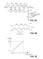
- FIG. 3Ashows a 2 stage, 2 branch version of a conventional Dickson type charge pump that receives Vcc as its input voltage on the left and generates from it an output voltage on the right.
- the top branchhas a pair of capacitors 303 and 307 with top plates connected along the branch and bottom plates respectively connected to the non-overlapping clock signals CLK 1 and CLK 2 , such as those shown in FIG. 3B .
- the capacitors 303 and 307are connected between the series of transistors 301 , 305 , and 309 , which are all diode connected to keep the charge from flowing back to the left.
- the bottom branchis constructed of transistors 311 , 315 , and 319 and capacitors 313 and 317 arranged in the same manner as the top branch, but with the clocks reversed so the tow branches will alternately drive the output.
- the transistors in FIG. 3Aare connected to function as diodes, they are not ideal diodes, in the sense that there will be a voltage drop across each of transistors. Between the drain and source of each of these transistors will be a voltage drop. This voltage drop will be the threshold voltage, Vt, of the transistor when there is no current flowing and Vt+ ⁇ Vds when there is current, where extra drain-source voltage drop can become proportionately quite large as current increases. Consequently, these voltage drops will reduce the output voltage of a real charge pump below that of the idealized charge pump like that discussed above in the Background with respect to FIG. 1 .
- the number of stages in each branchcan be increased to just pump the voltage up higher and the later stages can be used to cancel the threshold voltages.
- Another examplecould be a four phase Vt cancellation scheme.
- these prior cancellation techniqueshave limitations of one sort or another. For example, increases in the number of stages results in increases for both the required layout area and power consumption. Further, as each subsequent transistor in the series is subjected to higher voltages, their respective voltage drops become higher and the incremental gain in each stage correspondingly diminishes. In a four phase Vt cancellation scheme, the clock skews used can be difficult to control due to mismatch and routings.
- the techniques presented herecancel the threshold voltage by introducing a threshold voltage cancellation section that has the same structure as the main section of the charge pump that supplies the output.
- the threshold voltage cancellation stageuses the outputs from the section of the main section that it is mirroring to control the transistors. This will be illustrated using an exemplary embodiment based on a voltage doubler type of charge pump, which has been found to particular for use as an efficient low voltage output charge pump, where, in this example, the goal is to generate a target output of 4 volts from an input voltage of 2.5 volts.
- the sort of Dickson pump of FIG. 3is the basic architecture for a charge pump; however, for these sorts of values, Dickson pumps have relatively large die size, higher Icc consumption and less efficiency. Normal Vt cancellation schemes are difficult to apply to such architectures. As noted above, these are normally implemented with Dickson pump by pumping to higher than 4 volts in order to meet the design requirement and overcome the higher internal impendence.
- FIG. 4Ashows the exemplary embodiment.
- the main, or output, pump sectionprovides the output to drive the load and has the structure of a voltage doubler.
- the input voltage Vccis provided to both branches and through transistor 401 to node N 1 in the first branch and through transistor 403 to node N 2 in the second branch.
- the control gates of each of these transistorsis then attached to receive the voltage on the other branch, with the gate of 403 to node N 1 and the gate of 401 to N 2 .
- Each of the nodesis also coupled to a capacitor, respectively capacitor 405 driven by the clock signal CLK 1 and capacitor 407 driven by the clock signal CLK 2 .
- the clock signalsare again non-overlapping clocks such as shown in FIG. 4B .
- the clock signalscan be generated in any of the known manners. As the clocks alternate, the output of each branch will alternately (ideally) provide a doubled output voltage from the nodes N 1 and N 2 , which are then combined to form the pump output.
- the nodes N 1 and N 2are respectively connected to the output through transistors 421 and 423 .
- these two transistorswould be connected as diodes, having their control gates connected to also receive the voltages on N 1 and N 2 , respectively.
- thiswould result in the sort of voltage drops described above.
- a threshold voltage cancellation sectionas shown on the left side of FIG. 4A is introduced to supply the control gate voltages for these output transistors 421 and 423 .
- the Vt cancellation sectionhas the same structure and the output section and mirrors its function.
- a first branchincludes transistor 411 and capacitor 415 and a second branch includes transistor 413 and capacitor 417 , with the control gates of the transistor in each branch cross-coupled to the output node of the other branch.
- the output of each branch of the threshold cancellation stageis used to drive the output transistor of the corresponding branch in the output section: the node N 11 of the cancellation section is used for the control gate voltage of transistor 421 and the node N 22 of the cancellation section is used for the control gate voltage of transistor 423 .
- the capacitors in the cancellation sectionare clocked the same as the same element that they mirror in the output section, when the node N 1 of the output section is high, the node N 11 in the cancellation section will also be high, so that transistor 421 is on and the output voltage passed; N 1 and N 11 will similarly be low at the same time, so that 421 is turned off to prevent the back flow of charge.
- the nodes N 2 , N 22 and transistor 423function similarly.
- this sort of arrangement for the cancellation of thresholdcan be used charge pump types. More generally, when used with other designs, in addition to the output section, which will be formed with the same architecture as usual, there will also be a voltage threshold cancellation section formed with the same structure. In the main output section, the transistors typically connected as diodes to charge from back flowing will now have their control gates connected to be set to a voltage from the mirrored node in the voltage cancellation section. For example, going back to FIG. 3 A, taking the shown Dickson pump as the output section, a voltage cancellation stage of the same structure (less transistors 309 and 319 , which take the role of 421 and 423 in FIG. 4A ) would also be included. The level on the equivalent of the top plate of 307 on the cancellation stage would control the gate of 309 , the level on the equivalent of the top plate of 303 would control the gate of 305 , and so on for the other branch.
- the various mirrored elements of the circuitsneed not have the same size since the elements of the output stage need to drive the load of the charge pump, whereas those of the cancellation are only driving some control gates.
- the transistors 401 and 403 and capacitors 405 and 407need provide sufficient output for the application (e.g., 4 volts and 2 mA).
- the transistors 411 and 413 and capacitors 415 and 417need only provide sufficient output for the control gate voltage of transistors 421 and 423 . For example, if the transistors in the cancellation stages need only be sized a tenth or twentieth that of the elements they mirror in the output stage.
- the exemplary embodiment of FIG. 4Ahas been found to be of higher efficiency for the target values (output of 2 mA at 4V with an input voltage of 2.5V). More specifically, using a voltage doubler for both the main and the Vt cancellation stage yields about twice the efficiency, with 50% less input current (Icc) consumption. Area efficiency is also improve as the doubler type design can provide these values with less stages, yielding an area efficiency requirement of about 40% that of a conventional Dickson pump.
- the scheme presented herealso has a number of other advantages. Unlike other Vt cancellation techniques, there is no requirement of the main, output section's stages to cancel the Vts, as the cancellation section handles this. There is also no reliance on complex clock phases or skews since the two pump sections operate in phase with each other. Additionally, the use of identical structures for the two sections results in a better and easier layout matching and clock skew matching of the pump clocks. In particular, the simple design and simple layout requirements are a distinct practical advantage.
- FIGS. 5-7can help illustrate the efficient of the exemplary embodiment as a low output voltage pump.
- FIG. 5shows a comparison of the output I-V curve for the exemplary embodiment versus a conventional pump design.
- the operation regionwill typically be for voltages of 4.5V or less, as the design is particularly effective between 3V and 4V.
- the design of FIG. 4Acan have its number of stages expanded.
- FIG. 6shows a comparison of the output (Iout/Iin) versus Vout curve for the exemplary embodiment versus a conventional pump design.
- FIG. 7shows a comparison of the output (Iout/area) versus Vout curve for the exemplary embodiment versus a conventional pump design.
- the charge pumpcan have multiple stages. Multi-stage charge pumps and, in the exemplary embodiment, a multi-stage implementation of the sort of design described above with respect to FIGS. 4A and 4B are considered.
- FIG. 8Ashows a branch of a four stage Dickson-type charge pump and some of the regulation circuitry.
- a series of diodes 801 , 805 , 809 , 813 and 817are connected in series with a capacitor ( 803 , 807 , 811 , 815 ,) having a top plate connected between each pair of diodes.
- the bottom plates of the capacitorsalternately receive the non-overlapping clock signals CLK 1 and CLK 2 . In this way, the output generates the level Vout from the input VCC.
- FIG. 8Ashows a branch of a four stage Dickson-type charge pump and some of the regulation circuitry.
- a series of diodes 801 , 805 , 809 , 813 and 817here implemented as diode connected transistors are connected in series with a capacitor ( 803 , 807 , 811 , 815 ,) having a top plate connected between each pair of diodes.
- the bottom plates of the capacitorsalternately receive the non
- the outputcan be fed into a voltage divider, here formed of resistors R 1 821 and R 2 823 , to provide a lower voltage (Vdiv) that can be compared to the reference value Vref by Amp 825 to generate the signal Control for regulating the pump, much as described above with respect to FIGS. 2 and 3 .
- Voutmay need to range from 4 volts up to 28 volts for erasing or programming in operation.
- the number of stages used for the pumpis based upon the highest voltage, in this example 28 volts.
- the regulation circuitrythen varies the operation of the pump to provide the desired output level, as illustrated schematically in FIG. 8C .
- the desired output Vout over the exemplary 4 volt to 28 volt rangeis plotted against the corresponding Control signal, here converted to a digital value ranging from 00 to FF in this example.
- the regulationcan then be implemented by any of the standard, such as varying the clock frequency (1/tosc), clock amplitude (Vclock), pump input (VCC), etc.
- Voutoperates at 4 volts with 10 stages is much less efficient than if operated at 4 volts with only 2 stages.
- having more stages than needed for the lower voltage outputsresults in a large amount of noise and higher power usage when operating at the lower voltage levels. Consequently, although a traditional charge pump needs to have enough stages to be able to provide the highest needed output value, when operating at lower values it will not as efficient as, and noisier than, a pump specific to the lower output.
- a charge pump systemwhere the number of stages active in boosting the output voltage is automatically self-adaptive based on the desired output.
- the exemplary embodimentis based on a multi-stage implementation of the design of FIG. 4B .
- the number of stageis chosen is still based on the maximum output wanted from the design, but when regulated to provide lower output levels, the later stages progressively drop out, so that although the stages are still there, they no longer perform a pumping function and instead act as filtering stages to further reduce noise.
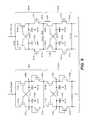
- FIG. 9illustrates an exemplary embodiment.
- a multiple number of main, or output, pump stagesare connected in series, with the output of one stage in the series connected as input the next state.
- Only two of the stages, 951 a and 951 bare explicitly shown to keep the figure manageable and each of the stages has the same structure as on the right hand side of FIG. 4A , but rearranged slight for convenience. (Basically, the placement of the capacitors and output nodes have been swapped between the representations.)
- For the first stage in the serieswill be the input voltage, such a Vcc, and the output of the last main stage in the series will be the output for the pump.
- the legs of each main stageare connected to supply the stages output though a corresponding pair of switches controlled by a corresponding gate stage.
- the two or more gate stagesare shown, with 961 a and 961 b corresponding to 951 a and 951 b .
- These gate stagesare (again after some rearrangement) the same as shown on the left of FIG. 4A .
- the output of one stageis supplied from the each of legs through a corresponding diode to provide the input of the next gate stage and the level on each leg (prior to the diode) controls the corresponding switch on the main, output stage side (the explicit connection is not shown to keep the e diagram manageable).
- thisshows a voltage double-type structure having a cross-coupled left and right legs that receive the input Va,in, that is either the input level of the pump (for the first stage) or the output of the previous stage (for all stages after the first).
- the left and right legsrespectively have transistors 401 a , 403 a whose control gates are connected to other leg below these transistors.
- the gates of 401 a , 403 aare also respected connected to the top plates of the capacitors 405 a , 407 a , which in turn have there respective bottom plates driven by the non-overlapping clock signals CLK 1 , CLK 2 .
- the output of the two legsare then combined through the transistors 421 a , 423 a that are respectively controlled by the levels on the nodes N 1 a , N 2 a of the corresponding gate stage 961 a to provide the output Va,out for stage 951 a , which then acts as the input Vb,in for the next stage.
- the threshold voltage on the pass gates 421 a , 423 bis cancelled, as described above with respect FIGS. 4A and 4B and the subsequent discussion.
- the last stage in the serieswill then provide the output for the pump.
- each of theseagain has a cross-coupled structure similar to that of the corresponding main output stage, as is also discussed in more detail above.
- the gates stagesare connected in series, with each stage's output supplying the next stage's input, except for first, which receives an initial input, and the last, which is only connected to control the pass gates of the last stage (much as shown on the left side of FIG. 4A ).
- the legs of the gate stages in the seriesare connected through a pass gate to provide the input to the next stage.
- the pass gatesare implemented as the diode connected transistors 431 a , 433 a and 431 b , 433 b , although other implementations could use an additional Vt cancellation arrangement for some or all of these pass gates as well. It should be noted that for the gate stages the load is fixed, and that there is no DC current load, only a capacitive load from the pass gates ( 421 , 423 ) on the main, output stage side.
- FIG. 9shows that it has another advantage, namely that at each stage the voltage is self-adapted to settle by the final output voltage being regulated into using the appropriate number of stages for the desired of output.
- the output regulationis varying from, for example, 4 volts to 28 volts as shown
- the number of stages, when all activeis selected to be able to provide the highest value of 28 volts; but, when regulated for lower output, the circuit of FIG. 9 will settle to the optimum number of pump stages, which will lead to the minimum charge pump output impedance.
- Thisis achieved in a self-adaptive manner, without the system needing to determine how many stages it wants to be active and generating as set of control signals to achieve this.
- Thisis distinct from the sort of prior art variable stage charge pump systems, such as those of U.S. Pat. Nos. 6,370,075 and 6,486,728, where control circuitry must determine the desired number of stages wanted to be active and then asserts a set of corresponding control signals to effect this.
- the subsequent gate stages( 961 b and any later gate stages) will continue to boost the levels (e.g., N 1 b , N 2 b ) used on the pass gates (e.g., 421 b , 423 b ) of the main stages down stream from 951 a , such as 951 b .
- the pass gates 421 b and 423 bAs well as any subsequent ones, being left on.
- main stage 951 b and subsequent stagesno longer are active to boost the output, but instead now act as filters of this output.
- 951 bwill self-adaptively revert back to a pumping function in the reverse manner.
- stage 951 bThis sort of transition of a pump stage, from being active as a pumping stage into performing a filtering function and back into pumping stage, described with respect to stage 951 b will similarly in a self-adaptive way for the other stages of the pump, starting with the last of the main output stages in the series.
- the number of stages for both the gate stages and main stagesare selected to be able provide the highest needed output.
- the pumpneeds to provide an output voltage over the 4V-28V range again and that to produce the 28 volt level uses six stages. When 28V are needed, all six stages are active pumping, but if the output drops to below, say, 25V, this can be reached with only five stages and the last will transition as described for stage 951 b .
- the fifth stagewould switch from actively pumping and both the last two stages would act as a filter capacitance, and so one until at the lowest output levels, only the first one or two stages are active in boosting, with the rest acting as a filtering capacitance.
- the stageswill kick back into the pumping mode in this self-adaptive manner.
- any of the various regulation schemescan be applied to the design here.
- the output voltage from the main stagecould be sampled and the Control signal can either be a logically value or an analog value.
- the Control signalcan be used to, say, control the input voltage supply level, the clock frequency, clock amplitude and so on to maintain the regulation level.
- the regulation control signalsuch as Control in FIG. 8A , would need to be used to alter the generation of the clock signals supplied to the pump, a sort of connection not explicitly represented in FIG. 2 .
- the regulation of the gate stagescan be done similarly to the output stages, or done independently with a separate regulator. It the gate stages are using the same regulation as the main stages, it may be desirable to have its output at the various stage to offset relative to the main stage output, using a diode for example.
Landscapes
- Engineering & Computer Science (AREA)
- Power Engineering (AREA)
- Dc-Dc Converters (AREA)
Abstract
Description
This application is a continuation-in-part of U.S. application Ser. No. 12/135,945 filed on Jun. 9, 2008, which is incorporated herein by reference in its entirety for all purposes.
This invention pertains generally to the field of charge pumps and more particularly to multi-stage charge pumps where the number of stages self-adjusts.
Charge pumps use a switching process to provide a DC output voltage larger or lower than its DC input voltage. In general, a charge pump will have a capacitor coupled to switches between an input and an output. During one clock half cycle, the charging half cycle, the capacitor couples in parallel to the input so as to charge up to the input voltage. During a second clock cycle, the transfer half cycle, the charged capacitor couples in series with the input voltage so as to provide an output voltage twice the level of the input voltage. This process is illustrated inFIGS. 1 aand1b. InFIG. 1 a, thecapacitor 5 is arranged in parallel with the input voltage VINto illustrate the charging half cycle. InFIG. 1 b, thecharged capacitor 5 is arranged in series with the input voltage to illustrate the transfer half cycle. As seen inFIG. 1 b, the positive terminal of thecharged capacitor 5 will thus be 2*VINwith respect to ground.
Charge pumps are used in many contexts. For example, they are used as peripheral circuits on flash and other non-volatile memories to generate many of the needed operating voltages, such as programming or erase voltages, from a lower power supply voltage. A number of charge pump designs, such as conventional Dickson-type pumps, are know in the art. But given the common reliance upon charge pumps, there is an on going need for improvements in pump design, particularly with respect to trying to reduce the amount of layout area and the efficiency of pumps.
A charge pump circuit for generating an output voltage is described. The charge pump includes N output generation stages, where N is an integer greater than one, each of which has a first branch receiving a first clock signal and providing a first output and a second branch receiving a second clock signal and providing a second output. The first and second clock signals are non-overlapping. The charge pump circuit also includes N corresponding gate stages, each having a first branch receiving the first clock signal and providing a first output and a second branch receiving the second clock signal and providing a second output, wherein the output generation stages and the corresponding gate stages have the same structure. The charge pump circuit further includes N corresponding first transistors and N corresponding second transistors. The output generation stages are connected in series with the first and second output of each of the output generation stages except the last in the series respectively connected through the corresponding first and second transistors to provide the input for the next output generation stage, the first and second outputs of the last in the series of output generation stages respectively connected through the corresponding first and second transistors to provide the output voltage of the charge pump. The gate stages are connected in series with the first and second output of each of the gate stages except the last in the series connected through a corresponding diode to provide the input for the next gate stage, and the first and second outputs of each of the gate stages respectively connected to the control gate the correspond first and second transistors.
According to another set of aspects, a charge pump system circuit for generating an output is described. The charge pump system includes N output generation stages and corresponding N gate stages, wherein the output generation stages and the corresponding gate stages have the same structure and N is an integer greater than one. The charge pump system further includes N corresponding switches. The output generation stages are connected in series with an output of each of the output generation stages except the last in the series being connected through the corresponding switch to provide an input for the next output generation stage, the output of the last in the series of output being connected through the corresponding switch to provide the output of the charge pump. The gate stages are connected in series with an output of each of the gate stages respectively connected to the control the correspond switch. The charge pump system also includes regulation circuitry connected to receive the output of the charge pump and to regulate the operation of the output generation stages based upon said output of the charge pump, whereby the number of output generation stages active in boosting the output is automatically adjusted.
Various aspects, advantages, features and embodiments of the present invention are included in the following description of exemplary examples thereof, which description should be taken in conjunction with the accompanying drawings. All patents, patent applications, articles, other publications, documents and things referenced herein are hereby incorporated herein by this reference in their entirety for all purposes. To the extent of any inconsistency or conflict in the definition or use of terms between any of the incorporated publications, documents or things and the present application, those of the present application shall prevail.
The various aspects and features of the present invention may be better understood by examining the following figures, in which:
The techniques presented here are widely applicable to various charge pump designs for the use of cancelling the threshold voltages of the switches (typically implemented as diodes in the prior art) used to prevent the backflow of charge after pump stages. In the following, the description will primarily be based on an exemplary embodiment using a voltage doubler-type of circuit, but the concepts can also be applied to other pump designs.
More information on prior art charge pumps, such as Dickson type pumps, and charge pumps generally, can be found, for example, in “Charge Pump Circuit Design” by Pan and Samaddar, McGraw-Hill, 2006, or “Charge Pumps: An Overview”, Pylarinos and Rogers, Department of Electrical and Computer Engineering University of Toronto, available on the webpage “www.eecg.toronto.edu/˜kphang/ece1371/chargepumps.pdf”. Further information on various other charge pump aspects and designs can be found in U.S. Pat. Nos. 5,436,587; 6,370,075; 6,556,465; 6,760,262; 6,922,096; 7,030,683; 7,554,311; 7,368,979; and 7,135,910; US Patent Publication numbers 2009-0153230-A1; 2009-0153232-A1; and 2009-0058506-A1; and applications Nos. 11/295,906 filed on Dec. 6, 2005; 11/303,387 filed on Dec. 16, 2005; 11/845,939, filed Aug. 28, 2007; 12/144,808 filed on Jun. 24, 2008; 12/135,948 filed Jun. 9, 2008; 12/146,243 filed Jun. 25, 2008; 12/337,050 filed Dec. 17, 2008; and 12/506,998 filed on Jul. 21, 2009. Examples of a pump system with a variable number of branches can be found, for example, in U.S. Pat. No. 5,781,473 and with a variable number of stages can be found, for example, in U.S. Pat. No. 6,370,075.
Although the transistors inFIG. 3A are connected to function as diodes, they are not ideal diodes, in the sense that there will be a voltage drop across each of transistors. Between the drain and source of each of these transistors will be a voltage drop. This voltage drop will be the threshold voltage, Vt, of the transistor when there is no current flowing and Vt+ΔVds when there is current, where extra drain-source voltage drop can become proportionately quite large as current increases. Consequently, these voltage drops will reduce the output voltage of a real charge pump below that of the idealized charge pump like that discussed above in the Background with respect toFIG. 1 .
Various methods are known to overcome this voltage drops. For example, the number of stages in each branch can be increased to just pump the voltage up higher and the later stages can be used to cancel the threshold voltages. Another example could be a four phase Vt cancellation scheme. However, these prior cancellation techniques have limitations of one sort or another. For example, increases in the number of stages results in increases for both the required layout area and power consumption. Further, as each subsequent transistor in the series is subjected to higher voltages, their respective voltage drops become higher and the incremental gain in each stage correspondingly diminishes. In a four phase Vt cancellation scheme, the clock skews used can be difficult to control due to mismatch and routings.
Instead, the techniques presented here cancel the threshold voltage by introducing a threshold voltage cancellation section that has the same structure as the main section of the charge pump that supplies the output. In the main section, rather than use the transistors connected as diodes, the threshold voltage cancellation stage uses the outputs from the section of the main section that it is mirroring to control the transistors. This will be illustrated using an exemplary embodiment based on a voltage doubler type of charge pump, which has been found to particular for use as an efficient low voltage output charge pump, where, in this example, the goal is to generate a target output of 4 volts from an input voltage of 2.5 volts.
More specifically, with an input voltage of Vcc=2.5 volts, to generate a 4 volt output supply able to deliver 2 mA output current, with minimum input current Ice and area requirements and good power efficiency is challenging. Normally, the sort of Dickson pump ofFIG. 3 is the basic architecture for a charge pump; however, for these sorts of values, Dickson pumps have relatively large die size, higher Icc consumption and less efficiency. Normal Vt cancellation schemes are difficult to apply to such architectures. As noted above, these are normally implemented with Dickson pump by pumping to higher than 4 volts in order to meet the design requirement and overcome the higher internal impendence.
To prevent the charge from flowing back from the output into the pump, the nodes N1 and N2 are respectively connected to the output throughtransistors FIG. 4A is introduced to supply the control gate voltages for theseoutput transistors
The Vt cancellation section has the same structure and the output section and mirrors its function. A first branch includestransistor 411 andcapacitor 415 and a second branch includestransistor 413 andcapacitor 417, with the control gates of the transistor in each branch cross-coupled to the output node of the other branch. The output of each branch of the threshold cancellation stage is used to drive the output transistor of the corresponding branch in the output section: the node N11 of the cancellation section is used for the control gate voltage oftransistor 421 and the node N22 of the cancellation section is used for the control gate voltage oftransistor 423. Since the capacitors in the cancellation section are clocked the same as the same element that they mirror in the output section, when the node N1 of the output section is high, the node N11 in the cancellation section will also be high, so thattransistor 421 is on and the output voltage passed; N1 and N11 will similarly be low at the same time, so that421 is turned off to prevent the back flow of charge. The nodes N2, N22 andtransistor 423 function similarly.
Although described here for a pump design based on a voltage doubler, this sort of arrangement for the cancellation of threshold can be used charge pump types. More generally, when used with other designs, in addition to the output section, which will be formed with the same architecture as usual, there will also be a voltage threshold cancellation section formed with the same structure. In the main output section, the transistors typically connected as diodes to charge from back flowing will now have their control gates connected to be set to a voltage from the mirrored node in the voltage cancellation section. For example, going back to FIG.3A, taking the shown Dickson pump as the output section, a voltage cancellation stage of the same structure (less transistors FIG. 4A ) would also be included. The level on the equivalent of the top plate of307 on the cancellation stage would control the gate of309, the level on the equivalent of the top plate of303 would control the gate of305, and so on for the other branch.
It should be noted that although the output section and the cancellation section have the same structure, the various mirrored elements of the circuits need not have the same size since the elements of the output stage need to drive the load of the charge pump, whereas those of the cancellation are only driving some control gates. Returning to the exemplary embodiment, thetransistors capacitors transistors capacitors transistors
Compared with a typical prior art design based upon a Dickson pump, the exemplary embodiment ofFIG. 4A has been found to be of higher efficiency for the target values (output of 2 mA at 4V with an input voltage of 2.5V). More specifically, using a voltage doubler for both the main and the Vt cancellation stage yields about twice the efficiency, with 50% less input current (Icc) consumption. Area efficiency is also improve as the doubler type design can provide these values with less stages, yielding an area efficiency requirement of about 40% that of a conventional Dickson pump.
The scheme presented here also has a number of other advantages. Unlike other Vt cancellation techniques, there is no requirement of the main, output section's stages to cancel the Vts, as the cancellation section handles this. There is also no reliance on complex clock phases or skews since the two pump sections operate in phase with each other. Additionally, the use of identical structures for the two sections results in a better and easier layout matching and clock skew matching of the pump clocks. In particular, the simple design and simple layout requirements are a distinct practical advantage.
Self-Adaptive Multi-Stage Implementation
As noted above, for higher outputs the charge pump can have multiple stages. Multi-stage charge pumps and, in the exemplary embodiment, a multi-stage implementation of the sort of design described above with respect toFIGS. 4A and 4B are considered.
First, the a multi-stage version of the sort of Dickson-type charge discussed above with respect toFIG. 3A is looked at some more to provide some context.FIG. 8A shows a branch of a four stage Dickson-type charge pump and some of the regulation circuitry. A series ofdiodes FIG. 8B illustrate the non-overlapping clock signals CLK1 and CLK2 having amplitude Vclock and period tosc. For regulating the charge pump, the output can be fed into a voltage divider, here formed ofresistors R1 821 andR2 823, to provide a lower voltage (Vdiv) that can be compared to the reference value Vref by Amp825 to generate the signal Control for regulating the pump, much as described above with respect toFIGS. 2 and 3 .
Charge pump systems are often called upon to generate a large range of output voltages Vpp from the pump output. For example, in an application as a peripheral element on a flash EEPROM memory, Vout may need to range from 4 volts up to 28 volts for erasing or programming in operation. In order to cover this range, the number of stages used for the pump is based upon the highest voltage, in this example 28 volts. The regulation circuitry then varies the operation of the pump to provide the desired output level, as illustrated schematically inFIG. 8C .
InFIG. 8C the desired output Vout over the exemplary 4 volt to 28 volt range is plotted against the corresponding Control signal, here converted to a digital value ranging from 00 to FF in this example. The regulation can then be implemented by any of the standard, such as varying the clock frequency (1/tosc), clock amplitude (Vclock), pump input (VCC), etc.
While the pump may need to supply a few pulses near 28 volts, the majority of the Vout pulses are typically at a much lower voltage. Pump output impedance is a function of the number of stages. As output impedance increases, the pump is less efficient. For example, Vout operates at 4 volts with 10 stages is much less efficient than if operated at 4 volts with only 2 stages. Also, having more stages than needed for the lower voltage outputs results in a large amount of noise and higher power usage when operating at the lower voltage levels. Consequently, although a traditional charge pump needs to have enough stages to be able to provide the highest needed output value, when operating at lower values it will not as efficient as, and noisier than, a pump specific to the lower output.
To overcome these shortcoming, a charge pump system is described where the number of stages active in boosting the output voltage is automatically self-adaptive based on the desired output. The exemplary embodiment is based on a multi-stage implementation of the design ofFIG. 4B . The number of stage is chosen is still based on the maximum output wanted from the design, but when regulated to provide lower output levels, the later stages progressively drop out, so that although the stages are still there, they no longer perform a pumping function and instead act as filtering stages to further reduce noise.
In more detail, looking thefirst stage 951aon the output side ofFIG. 9 , this shows a voltage double-type structure having a cross-coupled left and right legs that receive the input Va,in, that is either the input level of the pump (for the first stage) or the output of the previous stage (for all stages after the first). The left and right legs respectively havetransistors capacitors transistors corresponding gate stage 961ato provide the output Va,out forstage 951a, which then acts as the input Vb,in for the next stage. In this way, the threshold voltage on thepass gates FIGS. 4A and 4B and the subsequent discussion. The last stage in the series will then provide the output for the pump.
For the gate stages, each of these again has a cross-coupled structure similar to that of the corresponding main output stage, as is also discussed in more detail above. The gates stages are connected in series, with each stage's output supplying the next stage's input, except for first, which receives an initial input, and the last, which is only connected to control the pass gates of the last stage (much as shown on the left side ofFIG. 4A ). The legs of the gate stages in the series (excepting the last) are connected through a pass gate to provide the input to the next stage. InFIG. 9 , the pass gates are implemented as the diode connectedtransistors
In this way, higher output voltages can be generated in delivering power to the output, while still cancelling off the threshold voltages of the pass gates on the output side. An analysis of the arrangement ofFIG. 9 also shows that it has another advantage, namely that at each stage the voltage is self-adapted to settle by the final output voltage being regulated into using the appropriate number of stages for the desired of output.
More specifically, if the output regulation is varying from, for example, 4 volts to 28 volts as shown, the number of stages, when all active, is selected to be able to provide the highest value of 28 volts; but, when regulated for lower output, the circuit ofFIG. 9 will settle to the optimum number of pump stages, which will lead to the minimum charge pump output impedance. This is achieved in a self-adaptive manner, without the system needing to determine how many stages it wants to be active and generating as set of control signals to achieve this. This is distinct from the sort of prior art variable stage charge pump systems, such as those of U.S. Pat. Nos. 6,370,075 and 6,486,728, where control circuitry must determine the desired number of stages wanted to be active and then asserts a set of corresponding control signals to effect this.
To see how this occurs, consider the case where the circuit ofFIG. 9 is being regulated to generate an output voltage less than its maximum. The input voltage will be raised progressively though the main stages until it reaches the desired level for the output, which, if this value is sufficiently below the maximum, will happen before the last stage. Consider the case where the output ofstage 951a, Va,out, has reached this desired level. On the gate stage side, the nodes N1aand N2aof thecorresponding gate stage 961astill operate to controlpass gates pass gates main stage 951band subsequent stages no longer are active to boost the output, but instead now act as filters of this output. When a higher output is again needed,951bwill self-adaptively revert back to a pumping function in the reverse manner.
This sort of transition of a pump stage, from being active as a pumping stage into performing a filtering function and back into pumping stage, described with respect to stage951bwill similarly in a self-adaptive way for the other stages of the pump, starting with the last of the main output stages in the series. As noted before, the number of stages for both the gate stages and main stages are selected to be able provide the highest needed output. To take an example, say the pump needs to provide an output voltage over the 4V-28V range again and that to produce the 28 volt level uses six stages. When 28V are needed, all six stages are active pumping, but if the output drops to below, say, 25V, this can be reached with only five stages and the last will transition as described forstage 951b. Similarly, when the desired output drops 20V or less, the fifth stage would switch from actively pumping and both the last two stages would act as a filter capacitance, and so one until at the lowest output levels, only the first one or two stages are active in boosting, with the rest acting as a filtering capacitance. When the output is regulated back up, the stages will kick back into the pumping mode in this self-adaptive manner.
Consequently, as the output regulation is varied from 4V to 28V (or whatever the range is), the circuit will settle to the optimum number of pump stages, leading to a minimum charge pump output impendence. Under this arrangement, the pump impedance is self-adaptive to the output setting. There will consequently be less output noise due to the bypassed stages which also transition to a filtering capacitance. Such a minimizing of charge output impedance will lead can help to optimize the charge pump's performance. Consequently, in addition to the Vt cancellation for the transfer gates of the high voltage charge pump, this provides a simple scheme that is self adaptive to achieve the minimum output impedance and minimize output ripple, all without the need for some sort of control circuitry to somehow determine the desired number of stages and actively implement this somehow.
Concerning regulation, any of the various regulation schemes, such as those described above or in the various references cited above, can be applied to the design here. For example, the output voltage from the main stage could be sampled and the Control signal can either be a logically value or an analog value. The Control signal can be used to, say, control the input voltage supply level, the clock frequency, clock amplitude and so on to maintain the regulation level. (In this clock cases, the regulation control signal, such as Control inFIG. 8A , would need to be used to alter the generation of the clock signals supplied to the pump, a sort of connection not explicitly represented inFIG. 2 .) The regulation of the gate stages can be done similarly to the output stages, or done independently with a separate regulator. It the gate stages are using the same regulation as the main stages, it may be desirable to have its output at the various stage to offset relative to the main stage output, using a diode for example.
Although the invention has been described with reference to particular embodiments, the description is only an example of the invention's application and should not be taken as a limitation. Consequently, various adaptations and combinations of features of the embodiments disclosed are within the scope of the invention as encompassed by the following claims.
Claims (20)
1. A charge pump system circuit to generate an output voltage, including:
a plurality of N output generation stages, each having a first branch receiving a first clock signal and providing a first output and a second branch receiving a second clock signal and providing a second output, wherein the first and second clock signals are non-overlapping;
a corresponding plurality of N gate stages, each having a first branch receiving the first clock signal and providing a first output and a second branch receiving the second clock signal and providing a second output, wherein the output generation stages and the corresponding gate stages have the same structure; and
a corresponding plurality of N first transistors and a corresponding plurality N second transistors,
wherein the output generation stages are connected in series with the first and second output of each of the output generation stages except the last in the series respectively connected through the corresponding first and second transistors to provide the input for the next output generation stage, the first and second outputs of the last in the series of output generation stages respectively connected through the corresponding first and second transistors to provide the output voltage of the charge pump, and
wherein the gate stages are connected in series with the first and second output of each of the gate stages except the last in the series connected through a corresponding diode to provide the input for the next gate stage, the first and second outputs of each of the gate stages respectively connected to the control gate the correspond first and second transistors, and the first and second outputs of the last in the series being respectively connected to only the control gate the correspond first and second transistor, whereby the number of output generation stages active in boosting the output is automatically adjusted based upon said output of the charge pump.
2. The charge pump system circuit ofclaim 1 , wherein the first and second branches of each of the output generation stages and the gate stages respectively include a first and a second capacitor, the first clock signal being supplied to a plate of the first capacitor and the second clock signal being supplied to a plate of the second capacitor.
3. The charge pump system circuit ofclaim 1 , wherein circuit elements of the output generation stages are sized differently than the corresponding elements in the gate stages.
4. The charge pump system circuit ofclaim 1 , wherein the stages have a voltage doubler-type of structure.
5. The charge pump system circuit ofclaim 4 , wherein, for each of said stages, the first branch comprises:
a first transistor connected between an input voltage and a first output node from which the first output is provided, wherein a plate of the first capacitor not connected to receive the first clock signal is connected to the first output node; and
wherein the second branch comprises:
a second transistor connected between the input voltage and a second output node from which the second output is provided, wherein a plate of the second capacitor not connected to receive the second clock signal is connected to the second output node,
wherein the gate of the first transistor is connected to the second output node and the gate of the second transistor is connected to the first output node.
6. The charge pump system circuit ofclaim 5 , wherein the first and second transistors of the gate stages are sized smaller than the first and second transistors of the corresponding output generation stages.
7. The charge pump system circuit ofclaim 1 , further comprising:
regulation circuitry connected to receive the output of the charge pump and to regulate the operation of the output generation stages based upon said output of the charge pump.
8. The charge pump system ofclaim 7 , further comprising clock generation circuitry connected to the output generation stages to supply thereto a clock signal, the clock generation circuitry further connected to the regulation circuitry to receive a control signal derived from the output of the charge pump by the regulation circuitry, whereby the operation of the output generation stages are regulated.
9. The charge pump system ofclaim 8 , where the clock generation circuitry varies the frequency of the clock signal in response to the control signal.
10. The charge pump system ofclaim 8 , where the clock generation circuitry varies the amplitude of the clock signal in response to the control signal.
11. The charge pump system ofclaim 7 , wherein the regulation circuitry regulates the operation of the output generation stages by varying an input voltage level of the first of the output generation stages in response to the output of the charge pump.
12. The charge pump system ofclaim 7 , wherein the regulation circuitry regulates the gate stages independently of the output generation stages.
13. The charge pump system ofclaim 7 , wherein the regulation circuitry regulates the gate stages in the same manner as the output generation stages.
14. A charge pump system circuit to generate an output, including:
a plurality of N output generation stages;
a corresponding plurality of N gate stages, wherein the output generation stages and the corresponding gate stages have the same structure;
a corresponding plurality of N switches, wherein the output generation stages are connected in series with an output of each of the output generation stages except the last in the series being connected through the corresponding switch to provide an input for the next output generation stage, the output of the last in the series of output being connected through the corresponding switch to provide the output of the charge pump, and wherein the gate stages are connected in series with an output of each of the gate stages respectively connected to the control the corresponding switch, the output of the last gate stage in the series being only connected to drive the corresponding switch; and
regulation circuitry connected to receive the output of the charge pump and to regulate the operation of the output generation stages based upon said output of the charge pump,
wherein the number of output generation stages active in boosting the output is automatically adjusted based upon said output of the charge pump without being directly set by the regulation circuitry.
15. The charge pump system ofclaim 14 , further comprising clock generation circuitry connected to the output generation stages to supply thereto a clock signal, the clock generation circuitry further connected to the regulation circuitry to receive a control signal derived from the output of the charge pump by the regulation circuitry, whereby the operation of the output generation stages are regulated.
16. The charge pump system ofclaim 15 , where the clock generation circuitry varies the frequency of the clock signal in response to the control signal.
17. The charge pump system ofclaim 15 , where the clock generation circuitry varies the amplitude of the clock signal in response to the control signal.
18. The charge pump system ofclaim 14 , wherein the regulation circuitry regulates the operation of the output generation stages by varying an input voltage level of the first of the output generation stages in response to the output of the charge pump.
19. The charge pump system ofclaim 14 , wherein the regulation circuitry regulates the gate stages independently of the output generation stages.
20. The charge pump system ofclaim 14 , wherein the regulation circuitry regulates the gate stages in the same manner as the output generation stages.
Priority Applications (1)
| Application Number | Priority Date | Filing Date | Title |
|---|---|---|---|
| US12/570,646US7969235B2 (en) | 2008-06-09 | 2009-09-30 | Self-adaptive multi-stage charge pump |
Applications Claiming Priority (2)
| Application Number | Priority Date | Filing Date | Title |
|---|---|---|---|
| US12/135,945US20090302930A1 (en) | 2008-06-09 | 2008-06-09 | Charge Pump with Vt Cancellation Through Parallel Structure |
| US12/570,646US7969235B2 (en) | 2008-06-09 | 2009-09-30 | Self-adaptive multi-stage charge pump |
Related Parent Applications (1)
| Application Number | Title | Priority Date | Filing Date |
|---|---|---|---|
| US12/135,945Continuation-In-PartUS20090302930A1 (en) | 2008-06-09 | 2008-06-09 | Charge Pump with Vt Cancellation Through Parallel Structure |
Publications (2)
| Publication Number | Publication Date |
|---|---|
| US20100019832A1 US20100019832A1 (en) | 2010-01-28 |
| US7969235B2true US7969235B2 (en) | 2011-06-28 |
Family
ID=41568093
Family Applications (1)
| Application Number | Title | Priority Date | Filing Date |
|---|---|---|---|
| US12/570,646Expired - Fee RelatedUS7969235B2 (en) | 2008-06-09 | 2009-09-30 | Self-adaptive multi-stage charge pump |
Country Status (1)
| Country | Link |
|---|---|
| US (1) | US7969235B2 (en) |
Cited By (47)
| Publication number | Priority date | Publication date | Assignee | Title |
|---|---|---|---|---|
| US20110018617A1 (en)* | 2009-07-24 | 2011-01-27 | Khin Htoo | Charge Pump with Reduced Energy Consumption Through Charge Sharing and Clock Boosting Suitable for High Voltage Word Line in Flash Memories |
| US8294509B2 (en) | 2010-12-20 | 2012-10-23 | Sandisk Technologies Inc. | Charge pump systems with reduction in inefficiencies due to charge sharing between capacitances |
| US20120274393A1 (en)* | 2011-04-01 | 2012-11-01 | Stmicroelectronics S.R.I. | Dynamic biasing circuit for a protection stage using low voltage transistors |
| US8305807B2 (en) | 2010-07-09 | 2012-11-06 | Sandisk Technologies Inc. | Detection of broken word-lines in memory arrays |
| US8326256B1 (en)* | 2008-07-15 | 2012-12-04 | Impinj, Inc. | RFID tag with MOS bipolar hybrid rectifier |
| US8339185B2 (en) | 2010-12-20 | 2012-12-25 | Sandisk 3D Llc | Charge pump system that dynamically selects number of active stages |
| US8379454B2 (en) | 2011-05-05 | 2013-02-19 | Sandisk Technologies Inc. | Detection of broken word-lines in memory arrays |
| US8384467B1 (en) | 2012-03-22 | 2013-02-26 | Cypress Semiconductor Corporation | Reconfigurable charge pump |
| WO2013036342A1 (en) | 2011-09-09 | 2013-03-14 | Sandisk Technologies Inc. | Charge pump system dynamically reconfigurable for read and program |
| US8400212B1 (en) | 2011-09-22 | 2013-03-19 | Sandisk Technologies Inc. | High voltage charge pump regulation system with fine step adjustment |
| WO2013043269A2 (en) | 2011-09-22 | 2013-03-28 | Sandisk Technologies Inc. | Dynamic switching approach to reduce area and power consumption of high voltage charge pumps |
| US8432732B2 (en) | 2010-07-09 | 2013-04-30 | Sandisk Technologies Inc. | Detection of word-line leakage in memory arrays |
| US8514630B2 (en) | 2010-07-09 | 2013-08-20 | Sandisk Technologies Inc. | Detection of word-line leakage in memory arrays: current based approach |
| WO2014042820A1 (en) | 2012-09-14 | 2014-03-20 | Sandisk Technologies Inc. | Circuits for prevention of reverse leakage in vth-cancellation charge pumps |
| WO2014052163A1 (en) | 2012-09-27 | 2014-04-03 | Sandisk Technologies Inc. | Charge pump based over-sampling adc for current detection |
| US8710907B2 (en) | 2008-06-24 | 2014-04-29 | Sandisk Technologies Inc. | Clock generator circuit for a charge pump |
| US8730722B2 (en) | 2012-03-02 | 2014-05-20 | Sandisk Technologies Inc. | Saving of data in cases of word-line to word-line short in memory arrays |
| US8750042B2 (en) | 2011-07-28 | 2014-06-10 | Sandisk Technologies Inc. | Combined simultaneous sensing of multiple wordlines in a post-write read (PWR) and detection of NAND failures |
| US8775901B2 (en) | 2011-07-28 | 2014-07-08 | SanDisk Technologies, Inc. | Data recovery for defective word lines during programming of non-volatile memory arrays |
| US8847911B2 (en) | 2011-04-05 | 2014-09-30 | Cypress Semiconductor Corporation | Circuit to provide signal to sense array |
| US20150002214A1 (en)* | 2011-01-18 | 2015-01-01 | Peregrine Semiconductor Corporation | Differential Charge Pump |
| US8981835B2 (en)* | 2013-06-18 | 2015-03-17 | Sandisk Technologies Inc. | Efficient voltage doubler |
| US8994452B2 (en) | 2008-07-18 | 2015-03-31 | Peregrine Semiconductor Corporation | Low-noise high efficiency bias generation circuits and method |
| US9165683B2 (en) | 2013-09-23 | 2015-10-20 | Sandisk Technologies Inc. | Multi-word line erratic programming detection |
| US9190902B2 (en) | 2003-09-08 | 2015-11-17 | Peregrine Semiconductor Corporation | Low noise charge pump method and apparatus |
| US9195255B1 (en) | 2012-03-22 | 2015-11-24 | Parade Technologies, Ltd. | Reconfigurable charge pump |
| US9202593B1 (en) | 2014-09-02 | 2015-12-01 | Sandisk Technologies Inc. | Techniques for detecting broken word lines in non-volatile memories |
| US9240249B1 (en) | 2014-09-02 | 2016-01-19 | Sandisk Technologies Inc. | AC stress methods to screen out bit line defects |
| US9354654B2 (en) | 2011-05-11 | 2016-05-31 | Peregrine Semiconductor Corporation | High voltage ring pump with inverter stages and voltage boosting stages |
| US9443612B2 (en) | 2014-07-10 | 2016-09-13 | Sandisk Technologies Llc | Determination of bit line to low voltage signal shorts |
| US9449694B2 (en) | 2014-09-04 | 2016-09-20 | Sandisk Technologies Llc | Non-volatile memory with multi-word line select for defect detection operations |
| US9460809B2 (en) | 2014-07-10 | 2016-10-04 | Sandisk Technologies Llc | AC stress mode to screen out word line to word line shorts |
| US9484086B2 (en) | 2014-07-10 | 2016-11-01 | Sandisk Technologies Llc | Determination of word line to local source line shorts |
| US9514835B2 (en) | 2014-07-10 | 2016-12-06 | Sandisk Technologies Llc | Determination of word line to word line shorts between adjacent blocks |
| US9520776B1 (en) | 2015-09-18 | 2016-12-13 | Sandisk Technologies Llc | Selective body bias for charge pump transfer switches |
| US9647536B2 (en) | 2015-07-28 | 2017-05-09 | Sandisk Technologies Llc | High voltage generation using low voltage devices |
| US9659666B2 (en) | 2015-08-31 | 2017-05-23 | Sandisk Technologies Llc | Dynamic memory recovery at the sub-block level |
| US9660590B2 (en) | 2008-07-18 | 2017-05-23 | Peregrine Semiconductor Corporation | Low-noise high efficiency bias generation circuits and method |
| US9698676B1 (en) | 2016-03-11 | 2017-07-04 | Sandisk Technologies Llc | Charge pump based over-sampling with uniform step size for current detection |
| US9768683B2 (en) | 2011-01-18 | 2017-09-19 | Peregrine Semiconductor Corporation | Differential charge pump |
| US9810723B2 (en) | 2012-09-27 | 2017-11-07 | Sandisk Technologies Llc | Charge pump based over-sampling ADC for current detection |
| US9904403B2 (en) | 2015-06-30 | 2018-02-27 | Synaptics Incorporated | RF emission spectrum randomization and targeted nulling for an electronic device |
| US9917507B2 (en) | 2015-05-28 | 2018-03-13 | Sandisk Technologies Llc | Dynamic clock period modulation scheme for variable charge pump load currents |
| US9990979B2 (en) | 2015-10-02 | 2018-06-05 | Samsung Electronics Co., Ltd. | Semiconductor memory device capable of reducing peak current with respect to external power in multi-memory die structures |
| US10587267B2 (en)* | 2017-11-21 | 2020-03-10 | Texas Instruments Incorporated | Level shifter circuit generating bipolar clock signals |
| US12272419B2 (en) | 2022-10-12 | 2025-04-08 | Samsung Electronics Co., Ltd. | Charge pump having switch circuits for blocking leakage current during sudden power-off, and flash memory including the same |
| US12348132B2 (en) | 2023-02-16 | 2025-07-01 | SanDisk Technologies, Inc. | Stage based frequency optimization for area reduction of charge pumps |
Families Citing this family (16)
| Publication number | Priority date | Publication date | Assignee | Title |
|---|---|---|---|---|
| US20110133820A1 (en)* | 2009-12-09 | 2011-06-09 | Feng Pan | Multi-Stage Charge Pump with Variable Number of Boosting Stages |
| US8106701B1 (en) | 2010-09-30 | 2012-01-31 | Sandisk Technologies Inc. | Level shifter with shoot-through current isolation |
| US8537593B2 (en) | 2011-04-28 | 2013-09-17 | Sandisk Technologies Inc. | Variable resistance switch suitable for supplying high voltage to drive load |
| US8726104B2 (en) | 2011-07-28 | 2014-05-13 | Sandisk Technologies Inc. | Non-volatile memory and method with accelerated post-write read using combined verification of multiple pages |
| US8395434B1 (en) | 2011-10-05 | 2013-03-12 | Sandisk Technologies Inc. | Level shifter with negative voltage capability |
| US8836412B2 (en) | 2013-02-11 | 2014-09-16 | Sandisk 3D Llc | Charge pump with a power-controlled clock buffer to reduce power consumption and output voltage ripple |
| US9024680B2 (en) | 2013-06-24 | 2015-05-05 | Sandisk Technologies Inc. | Efficiency for charge pumps with low supply voltages |
| US9077238B2 (en) | 2013-06-25 | 2015-07-07 | SanDisk Technologies, Inc. | Capacitive regulation of charge pumps without refresh operation interruption |
| US9007046B2 (en) | 2013-06-27 | 2015-04-14 | Sandisk Technologies Inc. | Efficient high voltage bias regulation circuit |
| US9083231B2 (en) | 2013-09-30 | 2015-07-14 | Sandisk Technologies Inc. | Amplitude modulation for pass gate to improve charge pump efficiency |
| US9154027B2 (en) | 2013-12-09 | 2015-10-06 | Sandisk Technologies Inc. | Dynamic load matching charge pump for reduced current consumption |
| US9330776B2 (en) | 2014-08-14 | 2016-05-03 | Sandisk Technologies Inc. | High voltage step down regulator with breakdown protection |
| EP3319216A1 (en)* | 2016-11-03 | 2018-05-09 | GN Hearing A/S | Switched capacitor dc-dc power converter |
| DK3396833T3 (en)* | 2017-04-28 | 2019-11-18 | Gn Hearing As | Hearing aid comprising SWITCHED CAPACITOR-DC-DC CONVERTERS WITH LOW ELECTROMAGNETIC EMISSION |
| US11908521B2 (en) | 2022-02-01 | 2024-02-20 | Western Digital Technologies, Inc. | Non-volatile memory with redundant control line driver |
| WO2024097409A2 (en)* | 2022-11-04 | 2024-05-10 | Arizona Board Of Regents On Behalf Of The University Of Arizona | Context-aware circuit design for wearable biosymbiotic devices |
Citations (175)
| Publication number | Priority date | Publication date | Assignee | Title |
|---|---|---|---|---|
| US3697860A (en) | 1971-03-15 | 1972-10-10 | Westinghouse Electric Corp | Dc static switch circuit with a main switch device and a power sharing circuit portion |
| US4271488A (en) | 1979-04-13 | 1981-06-02 | Tektronix, Inc. | High-speed acquisition system employing an analog memory matrix |
| US4511811A (en) | 1982-02-08 | 1985-04-16 | Seeq Technology, Inc. | Charge pump for providing programming voltage to the word lines in a semiconductor memory array |
| US4583157A (en) | 1985-02-08 | 1986-04-15 | At&T Bell Laboratories | Integrated circuit having a variably boosted node |
| US4636748A (en) | 1985-06-26 | 1987-01-13 | Data General Corporation | Charge pump for use in a phase-locked loop |
| US4736121A (en) | 1985-09-10 | 1988-04-05 | Sos Microelettronica S.p.A. | Charge pump circuit for driving N-channel MOS transistors |
| US4742549A (en) | 1984-10-05 | 1988-05-03 | Elevator Gmbh | Procedure for watching over the area in front of a lift |
| US4888738A (en) | 1988-06-29 | 1989-12-19 | Seeq Technology | Current-regulated, voltage-regulated erase circuit for EEPROM memory |
| US4952821A (en) | 1987-06-12 | 1990-08-28 | Oki Electric Industry Co., Ltd. | Voltage detection circuit and comparison voltage generator therefor |
| US5008799A (en) | 1990-04-05 | 1991-04-16 | Montalvo Antonio J | Back-to-back capacitor charge pumps |
| US5036229A (en) | 1989-07-18 | 1991-07-30 | Gazelle Microcircuits, Inc. | Low ripple bias voltage generator |
| US5059815A (en) | 1990-04-05 | 1991-10-22 | Advanced Micro Devices, Inc. | High voltage charge pumps with series capacitors |
| US5103191A (en) | 1989-07-25 | 1992-04-07 | Siemens Aktiengesellschaft | Circuit configuration for phase locking |
| US5168174A (en) | 1991-07-12 | 1992-12-01 | Texas Instruments Incorporated | Negative-voltage charge pump with feedback control |
| US5175706A (en) | 1989-12-07 | 1992-12-29 | Sgs-Thomson Microelectronics S.A. | Programming voltage generator circuit for programmable memory |
| US5220531A (en) | 1991-01-02 | 1993-06-15 | Information Storage Devices, Inc. | Source follower storage cell and improved method and apparatus for iterative write for integrated circuit analog signal recording and playback |
| US5241494A (en) | 1990-09-26 | 1993-08-31 | Information Storage Devices | Integrated circuit system for analog signal recording and playback |
| US5263000A (en) | 1992-10-22 | 1993-11-16 | Advanced Micro Devices, Inc. | Drain power supply |
| US5301097A (en) | 1992-06-10 | 1994-04-05 | Intel Corporation | Multi-staged charge-pump with staggered clock phases for providing high current capability |
| US5363333A (en) | 1992-09-30 | 1994-11-08 | Nec Corporation | Dynamic random access memory device having power supply system appropriately biasing switching transistors and storage capacitors in burn-in testing process |
| US5388064A (en) | 1991-11-26 | 1995-02-07 | Information Storage Devices, Inc. | Programmable non-volatile analog voltage source devices and methods |
| US5392205A (en) | 1991-11-07 | 1995-02-21 | Motorola, Inc. | Regulated charge pump and method therefor |
| US5436587A (en) | 1993-11-24 | 1995-07-25 | Sundisk Corporation | Charge pump circuit with exponetral multiplication |
| US5483434A (en) | 1992-01-14 | 1996-01-09 | Seesink; Petrus H. | High voltage generator having output current control |
| US5483486A (en) | 1994-10-19 | 1996-01-09 | Intel Corporation | Charge pump circuit for providing multiple output voltages for flash memory |
| US5493249A (en) | 1993-12-06 | 1996-02-20 | Micron Technology, Inc. | System powered with inter-coupled charge pumps |
| US5508971A (en) | 1994-10-17 | 1996-04-16 | Sandisk Corporation | Programmable power generation circuit for flash EEPROM memory systems |
| US5521547A (en) | 1992-06-24 | 1996-05-28 | Nec Corporation | Boost voltage generating circuit |
| US5563779A (en) | 1994-12-05 | 1996-10-08 | Motorola, Inc. | Method and apparatus for a regulated supply on an integrated circuit |
| US5596532A (en) | 1995-10-18 | 1997-01-21 | Sandisk Corporation | Flash EEPROM self-adaptive voltage generation circuit operative within a continuous voltage source range |
| EP0756220A1 (en) | 1995-07-28 | 1997-01-29 | STMicroelectronics S.r.l. | Charge pump circuit with improved features |
| US5602794A (en) | 1995-09-29 | 1997-02-11 | Intel Corporation | Variable stage charge pump |
| US5623436A (en) | 1993-06-17 | 1997-04-22 | Information Storage Devices | Method and apparatus for adjustment and control of an iterative method of recording analog signals with on-chip trimming techniques |
| US5625544A (en) | 1996-04-25 | 1997-04-29 | Programmable Microelectronics Corp. | Charge pump |
| US5629646A (en) | 1995-03-21 | 1997-05-13 | Texas Instruments Incorporated | Apparatus and method for power reduction in dRAM units |
| US5629890A (en) | 1994-09-14 | 1997-05-13 | Information Storage Devices, Inc. | Integrated circuit system for analog signal storing and recovery incorporating read while writing voltage program method |
| US5638320A (en) | 1994-11-02 | 1997-06-10 | Invoice Technology, Inc. | High resolution analog storage EPROM and flash EPROM |
| US5680341A (en) | 1996-01-16 | 1997-10-21 | Invoice Technology | Pipelined record and playback for analog non-volatile memory |
| US5689201A (en) | 1995-08-08 | 1997-11-18 | Oregon State University | Track-and-hold circuit utilizing a negative of the input signal for tracking |
| US5699312A (en) | 1996-04-18 | 1997-12-16 | Altera Corporation | Programmable voltage supply circuitry |
| US5734286A (en) | 1993-05-19 | 1998-03-31 | Kabushiki Kaisha Toshiba | Driving device of charge pump circuit and driving pulse generation method thereof |
| US5745409A (en) | 1995-09-28 | 1998-04-28 | Invox Technology | Non-volatile memory with analog and digital interface and storage |
| US5748533A (en) | 1996-03-26 | 1998-05-05 | Invoice Technology, Inc. | Read circuit which uses a coarse-to-fine search when reading the threshold voltage of a memory cell |
| US5748534A (en) | 1996-03-26 | 1998-05-05 | Invox Technology | Feedback loop for reading threshold voltage |
| US5796293A (en) | 1995-11-13 | 1998-08-18 | Samsung Electronics Co., Ltd. | Voltage boosting circuits having backup voltage boosting capability |
| EP0860945A2 (en) | 1997-02-25 | 1998-08-26 | SHARP Corporation | Voltage level shifter circuit |
| US5801987A (en) | 1997-03-17 | 1998-09-01 | Motorola, Inc. | Automatic transition charge pump for nonvolatile memories |
| US5818757A (en) | 1996-07-22 | 1998-10-06 | Invox Technology | Analog and multi-level memory with reduced program disturb |
| US5818766A (en) | 1997-03-05 | 1998-10-06 | Integrated Silicon Solution Inc. | Drain voltage pump circuit for nonvolatile memory device |
| US5828596A (en) | 1996-09-26 | 1998-10-27 | Sharp Kabushiki Kaisha | Semiconductor memory device |
| US5828592A (en) | 1997-03-12 | 1998-10-27 | Information Storage Devices, Inc. | Analog signal recording and playback integrated circuit and message management system |
| US5864247A (en) | 1995-08-21 | 1999-01-26 | Matsushita Electronics Corporation | Voltage detection circuit, power-on/off reset circuit, and semiconductor device |
| EP0902525A2 (en) | 1997-09-12 | 1999-03-17 | Information Storage Devices, Inc. | Method and apparatus for reducing power supply current surges in a charge pump using a delayed clock line |
| US5943226A (en) | 1997-02-27 | 1999-08-24 | Lg Semicon Co., Ltd. | Bootstrap charge pump circuit |
| US5945870A (en) | 1996-07-18 | 1999-08-31 | Altera Corporation | Voltage ramp rate control circuit |
| US5969565A (en) | 1996-05-17 | 1999-10-19 | Nec Corporation | Voltage booster circuit |
| US5973546A (en) | 1996-06-27 | 1999-10-26 | Advanced Micro Devices, Inc. | Charge pump circuit architecture |
| US5977803A (en) | 1997-02-24 | 1999-11-02 | Mitsubishi Denki Kabushiki Kaisha | Capacitance type sensor interface circuit |
| US5982222A (en) | 1995-12-30 | 1999-11-09 | Samsung Electronics, Co., Ltd. | High voltage generating circuit for a semiconductor memory device |
| US5999040A (en) | 1997-03-19 | 1999-12-07 | Stmicroelectronics S.A. | Voltage booster circuit with controlled number of stages |
| US6008690A (en) | 1997-06-11 | 1999-12-28 | Nec Corporation | Booster circuit |
| US6018264A (en) | 1998-02-11 | 2000-01-25 | Lg Semicon Co., Ltd. | Pumping circuit with amplitude limited to prevent an over pumping for semiconductor device |
| US6023187A (en) | 1997-12-23 | 2000-02-08 | Mitsubishi Semiconductor America, Inc. | Voltage pump for integrated circuit and operating method thereof |
| US6026002A (en) | 1996-03-28 | 2000-02-15 | Siemens Aktiengesellschaft | Circuit configuration for supplying an electronic load circuit |
| US6031399A (en) | 1998-02-13 | 2000-02-29 | National Semiconductor Corporation | Selectively configurable analog signal sampler |
| US6104225A (en) | 1997-04-21 | 2000-08-15 | Fujitsu Limited | Semiconductor device using complementary clock and signal input state detection circuit used for the same |
| US6107862A (en) | 1997-02-28 | 2000-08-22 | Seiko Instruments Inc. | Charge pump circuit |
| US6134145A (en) | 1998-06-23 | 2000-10-17 | Sandisk Corporation | High data rate write process for non-volatile flash memories |
| US6154088A (en) | 1996-07-18 | 2000-11-28 | Micron Technology, Inc. | Clocking scheme and charge transfer switch for increasing the efficiency of a charge pump or other circuit |
| WO2001006336A1 (en) | 1999-07-15 | 2001-01-25 | Maxim Integrated Products, Inc. | Pulse frequency operation of regulated charge pumps |
| US6184726B1 (en) | 1998-06-30 | 2001-02-06 | Sandisk Corporation | Adjustable level shifter circuits for analog or multilevel memories |
| US6188590B1 (en)* | 1996-12-18 | 2001-02-13 | Macronix International Co., Ltd. | Regulator system for charge pump circuits |
| US6198645B1 (en) | 1998-07-02 | 2001-03-06 | National Semiconductor Corporation | Buck and boost switched capacitor gain stage with optional shared rest state |
| US6208198B1 (en) | 1998-10-27 | 2001-03-27 | Hyundai Electronics Industries Co., Ltd. | Drain voltage pumping circuit |
| US6249445B1 (en) | 1999-02-15 | 2001-06-19 | Nec Corporation | Booster including charge pumping circuit with its electric power consumption reduced and method of operating the same |
| US6249898B1 (en) | 1998-06-30 | 2001-06-19 | Synopsys, Inc. | Method and system for reliability analysis of CMOS VLSI circuits based on stage partitioning and node activities |
| US6285622B1 (en) | 1999-10-29 | 2001-09-04 | Mitsubishi Denki Kabushiki Kaisha | Semiconductor device |
| US6314025B1 (en) | 1998-06-23 | 2001-11-06 | Sandisk Corporation | High data rate write process for non-volatile flash memories |
| US6320796B1 (en) | 2000-11-10 | 2001-11-20 | Marvell International, Ltd. | Variable slope charge pump control |
| US6320428B1 (en) | 1997-02-26 | 2001-11-20 | Kabushiki Kaisha Toshiba | Semiconductor integrated circuit device |
| US6329869B1 (en)* | 1999-05-19 | 2001-12-11 | Nec Corporation | Semiconductor device with less influence of noise |
| US6344984B1 (en) | 1999-09-03 | 2002-02-05 | Nec Corporation | Voltage multiplier having an intermediate tap |
| US6344959B1 (en) | 1998-05-01 | 2002-02-05 | Unitrode Corporation | Method for sensing the output voltage of a charge pump circuit without applying a load to the output stage |
| US20020014908A1 (en) | 1998-12-21 | 2002-02-07 | Christl Lauterbach | Device for voltage multiplication with high efficiency, combination of the device with a battery-operated apparatus, and low-power loss generation of a programming voltage |
| US6359798B1 (en) | 2000-12-08 | 2002-03-19 | Samsung Electronics Co., Ltd. | Charge pump voltage converter |
| US6400202B1 (en) | 2000-02-10 | 2002-06-04 | International Business Machines Corporation | Programmable delay element and synchronous DRAM using the same |
| US6404274B1 (en) | 1998-04-09 | 2002-06-11 | Kabushiki Kaisha Toshiba | Internal voltage generating circuit capable of generating variable multi-level voltages |
| US20020075706A1 (en)* | 1990-04-06 | 2002-06-20 | Mosaid Technologies Incorporated | Boosted voltage supply |
| US6424570B1 (en) | 2001-06-26 | 2002-07-23 | Advanced Micro Devices, Inc. | Modulated charge pump with uses an analog to digital converter to compensate for supply voltage variations |
| US6445243B2 (en) | 2000-05-10 | 2002-09-03 | Sanyo Electric Co., Ltd. | Charge-pump circuit and control method thereof |
| US6456170B1 (en) | 1999-06-01 | 2002-09-24 | Fujitsu Limited | Comparator and voltage controlled oscillator circuit |
| US20020140463A1 (en) | 2001-03-15 | 2002-10-03 | Paul Cheung | Programmable soft-start control for charge pump |
| US6476666B1 (en)* | 2001-05-30 | 2002-11-05 | Alliance Semiconductor Corporation | Bootstrapped charge pump |
| US6486728B2 (en) | 2001-03-16 | 2002-11-26 | Matrix Semiconductor, Inc. | Multi-stage charge pump |
| US6518830B2 (en) | 2000-08-22 | 2003-02-11 | Stmicroelectronics S.R.L. | High efficiency electronic circuit for generating and regulating a supply voltage |
| US6525614B2 (en) | 2000-11-17 | 2003-02-25 | Sanyo Electric Co., Ltd. | Voltage boost system having feedback control |
| US6525949B1 (en) | 2000-12-22 | 2003-02-25 | Matrix Semiconductor, Inc. | Charge pump circuit |
| US6531792B2 (en) | 2001-04-10 | 2003-03-11 | Fujitsu Limited | DC-DC converter and storage apparatus |
| US6538930B2 (en) | 2001-01-09 | 2003-03-25 | Mitsubishi Denki Kabushiki Kaisha | Charge pump circuit for generating positive and negative voltage with reverse current prevention circuit and a nonvolatile memory using the same |
| US6545529B2 (en) | 2000-05-02 | 2003-04-08 | Hynix Semiconductor Inc. | High voltage generating circuit |
| US6577535B2 (en) | 2001-02-16 | 2003-06-10 | Sandisk Corporation | Method and system for distributed power generation in multi-chip memory systems |
| US20030128560A1 (en) | 2002-01-10 | 2003-07-10 | Saiki William John | High voltage generation and regulation system for digital multilevel nonvolatile memory |
| US6606267B2 (en) | 1998-06-23 | 2003-08-12 | Sandisk Corporation | High data rate write process for non-volatile flash memories |
| US20030214346A1 (en)* | 2002-02-25 | 2003-11-20 | Stmicroelectronics S.R.I. | Charge pump for negative voltages |
| US6724241B1 (en) | 2002-10-25 | 2004-04-20 | Atmel Corporation | Variable charge pump circuit with dynamic load |
| US6734718B1 (en) | 2002-12-23 | 2004-05-11 | Sandisk Corporation | High voltage ripple reduction |
| US6781440B2 (en) | 2002-02-18 | 2004-08-24 | Winbond Electronics Corp. | Charge pump circuit with voltage multiplier for boosting clock signal and method thereof |
| US6798274B2 (en) | 2002-03-27 | 2004-09-28 | Sanyo Electric Co., Ltd. | Booster and imaging device using booster |
| US6801454B2 (en) | 2002-10-01 | 2004-10-05 | Sandisk Corporation | Voltage generation circuitry having temperature compensation |
| US6834001B2 (en) | 2001-09-26 | 2004-12-21 | Sanyo Electric Co., Ltd. | Multi-stage switched capacitor DC-DC converter |
| US6859091B1 (en) | 2003-09-18 | 2005-02-22 | Maxim Integrated Products, Inc. | Continuous linear regulated zero dropout charge pump with high efficiency load predictive clocking scheme |
| US6878981B2 (en) | 2003-03-20 | 2005-04-12 | Tower Semiconductor Ltd. | Triple-well charge pump stage with no threshold voltage back-bias effect |
| US20050093614A1 (en)* | 2003-10-30 | 2005-05-05 | Dong-Uk Lee | Multi stage voltage pump circuit |
| US6891764B2 (en) | 2003-04-11 | 2005-05-10 | Intel Corporation | Apparatus and method to read a nonvolatile memory |
| US6894554B2 (en) | 2002-01-17 | 2005-05-17 | Seiko Epson Corporation | Step-up circuits |
| US6922096B2 (en) | 2003-08-07 | 2005-07-26 | Sandisk Corporation | Area efficient charge pump |
| US20050195017A1 (en)* | 2004-03-03 | 2005-09-08 | Tien-Tzu Chen | High efficiency charge pump with prevention from reverse current |
| US20050248386A1 (en) | 2004-05-10 | 2005-11-10 | Sandisk Corporation | Four phase charge pump operable without phase overlap with improved efficiency |
| US6975135B1 (en) | 2002-12-10 | 2005-12-13 | Altera Corporation | Universally programmable output buffer |
| US6990031B2 (en) | 2001-09-03 | 2006-01-24 | Elpida Memory, Inc. | Semiconductor memory device control method and semiconductor memory device |
| US7002381B1 (en) | 2001-12-11 | 2006-02-21 | Advanced Micro Devices, Inc. | Switched-capacitor controller to control the rise times of on-chip generated high voltages |
| US7023260B2 (en) | 2003-06-30 | 2006-04-04 | Matrix Semiconductor, Inc. | Charge pump circuit incorporating corresponding parallel charge pump stages and method therefor |
| US20060114053A1 (en) | 2004-11-30 | 2006-06-01 | Renesas Technology Corp. | Charge-pump-type power supply circuit |
| US7116154B2 (en) | 2003-08-06 | 2006-10-03 | Spansion Llc | Low power charge pump |
| US7120051B2 (en) | 2004-12-14 | 2006-10-10 | Sandisk Corporation | Pipelined programming of non-volatile memories using early data |
| US7129759B2 (en) | 2004-02-03 | 2006-10-31 | Nec Electronics Corporation | Integrated circuit including an overvoltage protection circuit |
| US20060244518A1 (en) | 2005-04-29 | 2006-11-02 | Hynix Semiconductor Inc. | Internal voltage generator |
| US7135911B2 (en) | 2000-05-24 | 2006-11-14 | Kabushiki Kaisha Toshiba | Potential detector and semiconductor integrated circuit |
| US7135910B2 (en) | 2002-09-27 | 2006-11-14 | Sandisk Corporation | Charge pump with fibonacci number multiplication |
| US20070001745A1 (en) | 2005-06-29 | 2007-01-04 | Chih-Jen Yen | Charge pump for generating arbitrary voltage levels |
| US20070069805A1 (en) | 2005-09-29 | 2007-03-29 | Hynix Semiconductor Inc. | Internal voltage generating circuit |
| US7208996B2 (en)* | 2004-03-26 | 2007-04-24 | Sanyo Electric Co., Ltd. | Charge pump circuit |
| US7224591B2 (en) | 2005-02-24 | 2007-05-29 | Sharp Kabushiki Kaisha | Charge pump DC/DC converter circuit |
| US7227780B2 (en) | 2004-11-30 | 2007-06-05 | Spansion Llc | Semiconductor device and control method thereof |
| US20070126494A1 (en) | 2005-12-06 | 2007-06-07 | Sandisk Corporation | Charge pump having shunt diode for improved operating efficiency |
| US20070139100A1 (en) | 2005-12-16 | 2007-06-21 | Sandisk Corporation | Voltage regulation with active supplemental current for output stabilization |
| US20070139099A1 (en) | 2005-12-16 | 2007-06-21 | Sandisk Corporation | Charge pump regulation control for improved power efficiency |
| US7239192B2 (en) | 2003-08-06 | 2007-07-03 | Stmicroelectronics Sa | Self-reparable device to generate a high voltage, and method for repairing a device to generate a high voltage |
| US7253676B2 (en) | 2003-12-25 | 2007-08-07 | Kabushiki Kaisha Toshiba | Semiconductor device and driving method of semiconductor device |
| US7259612B2 (en) | 2005-06-28 | 2007-08-21 | Atmel Corporation | Efficient charge pump for a wide range of supply voltages |
| US20070222498A1 (en) | 2006-03-24 | 2007-09-27 | Freescale Semiconductor Inc. | Slew rate control of a charge pump |
| US7276960B2 (en) | 2005-07-18 | 2007-10-02 | Dialog Semiconductor Gmbh | Voltage regulated charge pump with regulated charge current into the flying capacitor |
| US20070229149A1 (en) | 2006-03-30 | 2007-10-04 | Sandisk Corporation | Voltage regulator having high voltage protection |
| US20080024096A1 (en) | 2006-07-31 | 2008-01-31 | Sandisk Corporation | Hybrid charge pump regulation |
| US7345335B2 (en) | 2004-06-09 | 2008-03-18 | Kabushiki Kaisha Toshiba | Semiconductor integrated circuit, booster circuitry, and non-volatile semiconductor memory device |
| US7368979B2 (en) | 2006-09-19 | 2008-05-06 | Sandisk Corporation | Implementation of output floating scheme for hv charge pumps |
| US20080111604A1 (en) | 2005-03-17 | 2008-05-15 | Boerstler David W | Digital circuit to measure and/or correct duty cycles |
| US20080116963A1 (en) | 2006-11-20 | 2008-05-22 | Hynix Semiconductor Inc. | Clock control circuit and voltage pumping device using the same |
| US20080157852A1 (en) | 2006-12-29 | 2008-07-03 | Sandisk Corporation | Unified voltage generation apparatus with improved power efficiency |
| DE102007026290A1 (en) | 2006-12-28 | 2008-07-03 | Samsung Electronics Co., Ltd., Suwon | High voltage generating circuit, has regulator generating high voltage measuring current for measuring high voltage depending on level of high voltage, for controlling control signal, and for generating activation signal |
| US20080157859A1 (en) | 2006-12-29 | 2008-07-03 | Sandisk Corporation | Unified voltage generation method with improved power efficiency |
| US7397677B1 (en) | 2006-02-08 | 2008-07-08 | National Semiconductor Corporation | Apparatus and method for charge pump control with adjustable series resistance |
| US20080198662A1 (en) | 2007-02-20 | 2008-08-21 | Nima Mokhlesi | Dynamic verify based on threshold voltage distribution |
| US20080218134A1 (en) | 2007-03-08 | 2008-09-11 | Matsushita Electric Industrial Co., Ltd. | Power supply apparatus |
| US20080239802A1 (en) | 2007-03-30 | 2008-10-02 | Tyler Thorp | Device with Load-Based Voltage Generation |
| US20080239856A1 (en) | 2007-03-30 | 2008-10-02 | Tyler Thorp | Method for Load-Based Voltage Generation |
| US7443735B2 (en) | 2006-12-22 | 2008-10-28 | Sandisk Corporation | Method of reducing wordline recovery time |
| US20080278222A1 (en)* | 2006-07-19 | 2008-11-13 | Stmicroelectronics S.R.I. | Charge pump circuit |
| US7463521B2 (en) | 2005-04-01 | 2008-12-09 | Sandisk Corporation | Method for non-volatile memory with managed execution of cached data |
| US7468628B2 (en) | 2004-11-08 | 2008-12-23 | Hynix Semiconductor Inc. | Internal voltage generators for semiconductor memory device |
| US20090033306A1 (en) | 2007-08-02 | 2009-02-05 | Toru Tanzawa | Voltage trimming |
| US20090051413A1 (en)* | 2007-08-20 | 2009-02-26 | Taiwan Semiconductor Manufacturing Company, Ltd. | Apparatus and method for increasing charge pump efficiency |
| US20090058507A1 (en) | 2007-08-28 | 2009-03-05 | Prajit Nandi | Bottom Plate Regulated Charge Pump |
| US20090058506A1 (en) | 2007-08-28 | 2009-03-05 | Prajit Nandi | Bottom Plate Regulation of Charge Pumps |
| US20090091366A1 (en) | 2007-10-09 | 2009-04-09 | Hynix Semiconductor, Inc. | Voltage generator of semiconductor integrated circuit |
| US7521978B2 (en) | 2005-11-02 | 2009-04-21 | Hynix Semiconductor Inc. | Clock driver |
| US20090121780A1 (en) | 2007-11-12 | 2009-05-14 | Macronix International Co., Ltd. | Multiple-stage charge pump with charge recycle circuit |
| US20090153232A1 (en) | 2007-05-25 | 2009-06-18 | Atmel Corporation | Low voltage charge pump |
| US20090153231A1 (en) | 2007-12-12 | 2009-06-18 | Feng Pan | Diode Connected Regulation of Charge Pumps |
| US20090153230A1 (en) | 2007-12-12 | 2009-06-18 | Feng Pan | Low Voltage Charge Pump with Regulation |
| US20090167418A1 (en) | 2007-10-24 | 2009-07-02 | Vijay Raghavan | Supply Regulated Charge Pump System |
| US7579903B2 (en) | 2005-08-03 | 2009-08-25 | Nec Electronics Corporation | Power-source potential control circuit and method of trimming power-source potential |
| US20090219077A1 (en)* | 2008-02-29 | 2009-09-03 | Stefano Pietri | Voltage multiplier with improved efficiency |
| US7671572B2 (en) | 2006-04-07 | 2010-03-02 | Samsung Electronics Co. Ltd. | Voltage boost circuit and voltage boosting method using voltage boost clock signal with varying frequency |
| US20100244935A1 (en) | 2007-11-05 | 2010-09-30 | Electronics And Telecommunications Research Institute | High-voltage cmos charge pump |
- 2009
- 2009-09-30USUS12/570,646patent/US7969235B2/ennot_activeExpired - Fee Related
Patent Citations (204)
| Publication number | Priority date | Publication date | Assignee | Title |
|---|---|---|---|---|
| US3697860A (en) | 1971-03-15 | 1972-10-10 | Westinghouse Electric Corp | Dc static switch circuit with a main switch device and a power sharing circuit portion |
| US4271488A (en) | 1979-04-13 | 1981-06-02 | Tektronix, Inc. | High-speed acquisition system employing an analog memory matrix |
| US4511811A (en) | 1982-02-08 | 1985-04-16 | Seeq Technology, Inc. | Charge pump for providing programming voltage to the word lines in a semiconductor memory array |
| US4742549A (en) | 1984-10-05 | 1988-05-03 | Elevator Gmbh | Procedure for watching over the area in front of a lift |
| US4583157A (en) | 1985-02-08 | 1986-04-15 | At&T Bell Laboratories | Integrated circuit having a variably boosted node |
| US4636748A (en) | 1985-06-26 | 1987-01-13 | Data General Corporation | Charge pump for use in a phase-locked loop |
| US4736121A (en) | 1985-09-10 | 1988-04-05 | Sos Microelettronica S.p.A. | Charge pump circuit for driving N-channel MOS transistors |
| US4952821A (en) | 1987-06-12 | 1990-08-28 | Oki Electric Industry Co., Ltd. | Voltage detection circuit and comparison voltage generator therefor |
| US4888738A (en) | 1988-06-29 | 1989-12-19 | Seeq Technology | Current-regulated, voltage-regulated erase circuit for EEPROM memory |
| US5036229A (en) | 1989-07-18 | 1991-07-30 | Gazelle Microcircuits, Inc. | Low ripple bias voltage generator |
| US5103191A (en) | 1989-07-25 | 1992-04-07 | Siemens Aktiengesellschaft | Circuit configuration for phase locking |
| US5175706A (en) | 1989-12-07 | 1992-12-29 | Sgs-Thomson Microelectronics S.A. | Programming voltage generator circuit for programmable memory |
| US5059815A (en) | 1990-04-05 | 1991-10-22 | Advanced Micro Devices, Inc. | High voltage charge pumps with series capacitors |
| US5008799A (en) | 1990-04-05 | 1991-04-16 | Montalvo Antonio J | Back-to-back capacitor charge pumps |
| US20020075706A1 (en)* | 1990-04-06 | 2002-06-20 | Mosaid Technologies Incorporated | Boosted voltage supply |
| US5241494A (en) | 1990-09-26 | 1993-08-31 | Information Storage Devices | Integrated circuit system for analog signal recording and playback |
| US5220531A (en) | 1991-01-02 | 1993-06-15 | Information Storage Devices, Inc. | Source follower storage cell and improved method and apparatus for iterative write for integrated circuit analog signal recording and playback |
| US5168174A (en) | 1991-07-12 | 1992-12-01 | Texas Instruments Incorporated | Negative-voltage charge pump with feedback control |
| US5392205A (en) | 1991-11-07 | 1995-02-21 | Motorola, Inc. | Regulated charge pump and method therefor |
| US5388064A (en) | 1991-11-26 | 1995-02-07 | Information Storage Devices, Inc. | Programmable non-volatile analog voltage source devices and methods |
| US5483434A (en) | 1992-01-14 | 1996-01-09 | Seesink; Petrus H. | High voltage generator having output current control |
| US5301097A (en) | 1992-06-10 | 1994-04-05 | Intel Corporation | Multi-staged charge-pump with staggered clock phases for providing high current capability |
| US5521547A (en) | 1992-06-24 | 1996-05-28 | Nec Corporation | Boost voltage generating circuit |
| US5363333A (en) | 1992-09-30 | 1994-11-08 | Nec Corporation | Dynamic random access memory device having power supply system appropriately biasing switching transistors and storage capacitors in burn-in testing process |
| US5263000A (en) | 1992-10-22 | 1993-11-16 | Advanced Micro Devices, Inc. | Drain power supply |
| US5734286A (en) | 1993-05-19 | 1998-03-31 | Kabushiki Kaisha Toshiba | Driving device of charge pump circuit and driving pulse generation method thereof |
| US5623436A (en) | 1993-06-17 | 1997-04-22 | Information Storage Devices | Method and apparatus for adjustment and control of an iterative method of recording analog signals with on-chip trimming techniques |
| US5436587A (en) | 1993-11-24 | 1995-07-25 | Sundisk Corporation | Charge pump circuit with exponetral multiplication |
| US5493249A (en) | 1993-12-06 | 1996-02-20 | Micron Technology, Inc. | System powered with inter-coupled charge pumps |
| US5629890A (en) | 1994-09-14 | 1997-05-13 | Information Storage Devices, Inc. | Integrated circuit system for analog signal storing and recovery incorporating read while writing voltage program method |
| US5563825A (en) | 1994-10-17 | 1996-10-08 | Sandisk Corporation | Programmable power generation circuit for flash eeprom memory systems |
| US5592420A (en) | 1994-10-17 | 1997-01-07 | Sandisk Corporation | Programmable power generation circuit for flash EEPROM memory systems |
| US5568424A (en) | 1994-10-17 | 1996-10-22 | Sandisk Corporation | Programmable power generation circuit for flash EEPROM memory systems |
| US5508971A (en) | 1994-10-17 | 1996-04-16 | Sandisk Corporation | Programmable power generation circuit for flash EEPROM memory systems |
| US5693570A (en) | 1994-10-17 | 1997-12-02 | Sandisk Corporation | Process for manufacturing a programmable power generation circuit for flash EEPROM memory systems |
| US5621685A (en) | 1994-10-17 | 1997-04-15 | Sandisk Corporation | Programmable power generation circuit for flash EEPROM memory systems |
| US5483486A (en) | 1994-10-19 | 1996-01-09 | Intel Corporation | Charge pump circuit for providing multiple output voltages for flash memory |
| US5638320A (en) | 1994-11-02 | 1997-06-10 | Invoice Technology, Inc. | High resolution analog storage EPROM and flash EPROM |
| US5694356A (en) | 1994-11-02 | 1997-12-02 | Invoice Technology, Inc. | High resolution analog storage EPROM and flash EPROM |
| US5687115A (en) | 1994-11-02 | 1997-11-11 | Invoice Technology, Inc. | Write circuits for analog memory |
| US5563779A (en) | 1994-12-05 | 1996-10-08 | Motorola, Inc. | Method and apparatus for a regulated supply on an integrated circuit |
| US5629646A (en) | 1995-03-21 | 1997-05-13 | Texas Instruments Incorporated | Apparatus and method for power reduction in dRAM units |
| EP0756220A1 (en) | 1995-07-28 | 1997-01-29 | STMicroelectronics S.r.l. | Charge pump circuit with improved features |
| US5689201A (en) | 1995-08-08 | 1997-11-18 | Oregon State University | Track-and-hold circuit utilizing a negative of the input signal for tracking |
| US5864247A (en) | 1995-08-21 | 1999-01-26 | Matsushita Electronics Corporation | Voltage detection circuit, power-on/off reset circuit, and semiconductor device |
| US5745409A (en) | 1995-09-28 | 1998-04-28 | Invox Technology | Non-volatile memory with analog and digital interface and storage |
| US5801980A (en) | 1995-09-28 | 1998-09-01 | Invox Technology | Testing of an analog memory using an on-chip digital input/output interface |
| US5781473A (en) | 1995-09-29 | 1998-07-14 | Intel Corporation | Variable stage charge pump |
| US5732039A (en) | 1995-09-29 | 1998-03-24 | Intel Corporation | Variable stage charge pump |
| US5767735A (en) | 1995-09-29 | 1998-06-16 | Intel Corporation | Variable stage charge pump |
| US5602794A (en) | 1995-09-29 | 1997-02-11 | Intel Corporation | Variable stage charge pump |
| US5596532A (en) | 1995-10-18 | 1997-01-21 | Sandisk Corporation | Flash EEPROM self-adaptive voltage generation circuit operative within a continuous voltage source range |
| US5796293A (en) | 1995-11-13 | 1998-08-18 | Samsung Electronics Co., Ltd. | Voltage boosting circuits having backup voltage boosting capability |
| US5982222A (en) | 1995-12-30 | 1999-11-09 | Samsung Electronics, Co., Ltd. | High voltage generating circuit for a semiconductor memory device |
| US5680341A (en) | 1996-01-16 | 1997-10-21 | Invoice Technology | Pipelined record and playback for analog non-volatile memory |
| US5748533A (en) | 1996-03-26 | 1998-05-05 | Invoice Technology, Inc. | Read circuit which uses a coarse-to-fine search when reading the threshold voltage of a memory cell |
| US5748534A (en) | 1996-03-26 | 1998-05-05 | Invox Technology | Feedback loop for reading threshold voltage |
| US6026002A (en) | 1996-03-28 | 2000-02-15 | Siemens Aktiengesellschaft | Circuit configuration for supplying an electronic load circuit |
| US5699312A (en) | 1996-04-18 | 1997-12-16 | Altera Corporation | Programmable voltage supply circuitry |
| US5790469A (en) | 1996-04-18 | 1998-08-04 | Altera Corporation | Programmable voltage supply circuitry |
| US5625544A (en) | 1996-04-25 | 1997-04-29 | Programmable Microelectronics Corp. | Charge pump |
| US5969565A (en) | 1996-05-17 | 1999-10-19 | Nec Corporation | Voltage booster circuit |
| US5973546A (en) | 1996-06-27 | 1999-10-26 | Advanced Micro Devices, Inc. | Charge pump circuit architecture |
| US6154088A (en) | 1996-07-18 | 2000-11-28 | Micron Technology, Inc. | Clocking scheme and charge transfer switch for increasing the efficiency of a charge pump or other circuit |
| US5945870A (en) | 1996-07-18 | 1999-08-31 | Altera Corporation | Voltage ramp rate control circuit |
| US5818757A (en) | 1996-07-22 | 1998-10-06 | Invox Technology | Analog and multi-level memory with reduced program disturb |
| US5828596A (en) | 1996-09-26 | 1998-10-27 | Sharp Kabushiki Kaisha | Semiconductor memory device |
| US6188590B1 (en)* | 1996-12-18 | 2001-02-13 | Macronix International Co., Ltd. | Regulator system for charge pump circuits |
| US5977803A (en) | 1997-02-24 | 1999-11-02 | Mitsubishi Denki Kabushiki Kaisha | Capacitance type sensor interface circuit |
| EP0860945A2 (en) | 1997-02-25 | 1998-08-26 | SHARP Corporation | Voltage level shifter circuit |
| US6320428B1 (en) | 1997-02-26 | 2001-11-20 | Kabushiki Kaisha Toshiba | Semiconductor integrated circuit device |
| US5943226A (en) | 1997-02-27 | 1999-08-24 | Lg Semicon Co., Ltd. | Bootstrap charge pump circuit |
| US6107862A (en) | 1997-02-28 | 2000-08-22 | Seiko Instruments Inc. | Charge pump circuit |
| US5818766A (en) | 1997-03-05 | 1998-10-06 | Integrated Silicon Solution Inc. | Drain voltage pump circuit for nonvolatile memory device |
| US5828592A (en) | 1997-03-12 | 1998-10-27 | Information Storage Devices, Inc. | Analog signal recording and playback integrated circuit and message management system |
| US5801987A (en) | 1997-03-17 | 1998-09-01 | Motorola, Inc. | Automatic transition charge pump for nonvolatile memories |
| US5999040A (en) | 1997-03-19 | 1999-12-07 | Stmicroelectronics S.A. | Voltage booster circuit with controlled number of stages |
| US6104225A (en) | 1997-04-21 | 2000-08-15 | Fujitsu Limited | Semiconductor device using complementary clock and signal input state detection circuit used for the same |
| US6008690A (en) | 1997-06-11 | 1999-12-28 | Nec Corporation | Booster circuit |
| EP0902525A2 (en) | 1997-09-12 | 1999-03-17 | Information Storage Devices, Inc. | Method and apparatus for reducing power supply current surges in a charge pump using a delayed clock line |
| US6023187A (en) | 1997-12-23 | 2000-02-08 | Mitsubishi Semiconductor America, Inc. | Voltage pump for integrated circuit and operating method thereof |
| US6018264A (en) | 1998-02-11 | 2000-01-25 | Lg Semicon Co., Ltd. | Pumping circuit with amplitude limited to prevent an over pumping for semiconductor device |
| US6031399A (en) | 1998-02-13 | 2000-02-29 | National Semiconductor Corporation | Selectively configurable analog signal sampler |
| US6404274B1 (en) | 1998-04-09 | 2002-06-11 | Kabushiki Kaisha Toshiba | Internal voltage generating circuit capable of generating variable multi-level voltages |
| US6344959B1 (en) | 1998-05-01 | 2002-02-05 | Unitrode Corporation | Method for sensing the output voltage of a charge pump circuit without applying a load to the output stage |
| US6606267B2 (en) | 1998-06-23 | 2003-08-12 | Sandisk Corporation | High data rate write process for non-volatile flash memories |
| US6944058B2 (en) | 1998-06-23 | 2005-09-13 | Sandisk Corporation | High data rate write process for non-volatile flash memories |
| US6134145A (en) | 1998-06-23 | 2000-10-17 | Sandisk Corporation | High data rate write process for non-volatile flash memories |
| US6314025B1 (en) | 1998-06-23 | 2001-11-06 | Sandisk Corporation | High data rate write process for non-volatile flash memories |
| US6760262B2 (en) | 1998-06-30 | 2004-07-06 | Sandisk Corporation | Charge pump circuit adjustable in response to an external voltage source |
| US6249898B1 (en) | 1998-06-30 | 2001-06-19 | Synopsys, Inc. | Method and system for reliability analysis of CMOS VLSI circuits based on stage partitioning and node activities |
| US6208542B1 (en) | 1998-06-30 | 2001-03-27 | Sandisk Corporation | Techniques for storing digital data in an analog or multilevel memory |
| US6184726B1 (en) | 1998-06-30 | 2001-02-06 | Sandisk Corporation | Adjustable level shifter circuits for analog or multilevel memories |
| US6556465B2 (en) | 1998-06-30 | 2003-04-29 | Sandisk Corporation | Adjustable circuits for analog or multi-level memory |
| US6370075B1 (en) | 1998-06-30 | 2002-04-09 | Sandisk Corporation | Charge pump circuit adjustable in response to an external voltage source |
| US6185119B1 (en) | 1998-06-30 | 2001-02-06 | Sandisk Corporation | Analog memory IC with fully differential signal path |
| US6198645B1 (en) | 1998-07-02 | 2001-03-06 | National Semiconductor Corporation | Buck and boost switched capacitor gain stage with optional shared rest state |
| US6208198B1 (en) | 1998-10-27 | 2001-03-27 | Hyundai Electronics Industries Co., Ltd. | Drain voltage pumping circuit |
| US20020014908A1 (en) | 1998-12-21 | 2002-02-07 | Christl Lauterbach | Device for voltage multiplication with high efficiency, combination of the device with a battery-operated apparatus, and low-power loss generation of a programming voltage |
| US6249445B1 (en) | 1999-02-15 | 2001-06-19 | Nec Corporation | Booster including charge pumping circuit with its electric power consumption reduced and method of operating the same |
| US6329869B1 (en)* | 1999-05-19 | 2001-12-11 | Nec Corporation | Semiconductor device with less influence of noise |
| US6456170B1 (en) | 1999-06-01 | 2002-09-24 | Fujitsu Limited | Comparator and voltage controlled oscillator circuit |
| WO2001006336A1 (en) | 1999-07-15 | 2001-01-25 | Maxim Integrated Products, Inc. | Pulse frequency operation of regulated charge pumps |
| US6344984B1 (en) | 1999-09-03 | 2002-02-05 | Nec Corporation | Voltage multiplier having an intermediate tap |
| US6285622B1 (en) | 1999-10-29 | 2001-09-04 | Mitsubishi Denki Kabushiki Kaisha | Semiconductor device |
| US6400202B1 (en) | 2000-02-10 | 2002-06-04 | International Business Machines Corporation | Programmable delay element and synchronous DRAM using the same |
| US6545529B2 (en) | 2000-05-02 | 2003-04-08 | Hynix Semiconductor Inc. | High voltage generating circuit |
| US6445243B2 (en) | 2000-05-10 | 2002-09-03 | Sanyo Electric Co., Ltd. | Charge-pump circuit and control method thereof |
| US7135911B2 (en) | 2000-05-24 | 2006-11-14 | Kabushiki Kaisha Toshiba | Potential detector and semiconductor integrated circuit |
| US6518830B2 (en) | 2000-08-22 | 2003-02-11 | Stmicroelectronics S.R.L. | High efficiency electronic circuit for generating and regulating a supply voltage |
| US6320796B1 (en) | 2000-11-10 | 2001-11-20 | Marvell International, Ltd. | Variable slope charge pump control |
| US6525614B2 (en) | 2000-11-17 | 2003-02-25 | Sanyo Electric Co., Ltd. | Voltage boost system having feedback control |
| US6359798B1 (en) | 2000-12-08 | 2002-03-19 | Samsung Electronics Co., Ltd. | Charge pump voltage converter |
| US6525949B1 (en) | 2000-12-22 | 2003-02-25 | Matrix Semiconductor, Inc. | Charge pump circuit |
| US6538930B2 (en) | 2001-01-09 | 2003-03-25 | Mitsubishi Denki Kabushiki Kaisha | Charge pump circuit for generating positive and negative voltage with reverse current prevention circuit and a nonvolatile memory using the same |
| US6577535B2 (en) | 2001-02-16 | 2003-06-10 | Sandisk Corporation | Method and system for distributed power generation in multi-chip memory systems |
| US20020140463A1 (en) | 2001-03-15 | 2002-10-03 | Paul Cheung | Programmable soft-start control for charge pump |
| US6486728B2 (en) | 2001-03-16 | 2002-11-26 | Matrix Semiconductor, Inc. | Multi-stage charge pump |
| US6531792B2 (en) | 2001-04-10 | 2003-03-11 | Fujitsu Limited | DC-DC converter and storage apparatus |
| US6476666B1 (en)* | 2001-05-30 | 2002-11-05 | Alliance Semiconductor Corporation | Bootstrapped charge pump |
| US6424570B1 (en) | 2001-06-26 | 2002-07-23 | Advanced Micro Devices, Inc. | Modulated charge pump with uses an analog to digital converter to compensate for supply voltage variations |
| US6990031B2 (en) | 2001-09-03 | 2006-01-24 | Elpida Memory, Inc. | Semiconductor memory device control method and semiconductor memory device |
| US6834001B2 (en) | 2001-09-26 | 2004-12-21 | Sanyo Electric Co., Ltd. | Multi-stage switched capacitor DC-DC converter |
| US7002381B1 (en) | 2001-12-11 | 2006-02-21 | Advanced Micro Devices, Inc. | Switched-capacitor controller to control the rise times of on-chip generated high voltages |
| US20030128560A1 (en) | 2002-01-10 | 2003-07-10 | Saiki William John | High voltage generation and regulation system for digital multilevel nonvolatile memory |
| US6894554B2 (en) | 2002-01-17 | 2005-05-17 | Seiko Epson Corporation | Step-up circuits |
| US6781440B2 (en) | 2002-02-18 | 2004-08-24 | Winbond Electronics Corp. | Charge pump circuit with voltage multiplier for boosting clock signal and method thereof |
| US20030214346A1 (en)* | 2002-02-25 | 2003-11-20 | Stmicroelectronics S.R.I. | Charge pump for negative voltages |
| US6819162B2 (en)* | 2002-02-25 | 2004-11-16 | Stmicroelectronics S.R.L. | Charge pump for negative voltages |
| US6798274B2 (en) | 2002-03-27 | 2004-09-28 | Sanyo Electric Co., Ltd. | Booster and imaging device using booster |
| US7135910B2 (en) | 2002-09-27 | 2006-11-14 | Sandisk Corporation | Charge pump with fibonacci number multiplication |
| US6801454B2 (en) | 2002-10-01 | 2004-10-05 | Sandisk Corporation | Voltage generation circuitry having temperature compensation |
| US6724241B1 (en) | 2002-10-25 | 2004-04-20 | Atmel Corporation | Variable charge pump circuit with dynamic load |
| US6975135B1 (en) | 2002-12-10 | 2005-12-13 | Altera Corporation | Universally programmable output buffer |
| US6734718B1 (en) | 2002-12-23 | 2004-05-11 | Sandisk Corporation | High voltage ripple reduction |
| US7116155B2 (en) | 2002-12-23 | 2006-10-03 | Sandisk Corporation | High voltage ripple reduction and substrate protection |
| US6878981B2 (en) | 2003-03-20 | 2005-04-12 | Tower Semiconductor Ltd. | Triple-well charge pump stage with no threshold voltage back-bias effect |
| US6891764B2 (en) | 2003-04-11 | 2005-05-10 | Intel Corporation | Apparatus and method to read a nonvolatile memory |
| US7023260B2 (en) | 2003-06-30 | 2006-04-04 | Matrix Semiconductor, Inc. | Charge pump circuit incorporating corresponding parallel charge pump stages and method therefor |
| US7239192B2 (en) | 2003-08-06 | 2007-07-03 | Stmicroelectronics Sa | Self-reparable device to generate a high voltage, and method for repairing a device to generate a high voltage |
| US7116154B2 (en) | 2003-08-06 | 2006-10-03 | Spansion Llc | Low power charge pump |
| US6922096B2 (en) | 2003-08-07 | 2005-07-26 | Sandisk Corporation | Area efficient charge pump |
| US7113023B2 (en) | 2003-08-07 | 2006-09-26 | Sandisk Corporation | Area efficient charge pump |
| US20050237103A1 (en)* | 2003-08-07 | 2005-10-27 | Raul-Adrian Cernea | Area efficient charge pump |
| US6859091B1 (en) | 2003-09-18 | 2005-02-22 | Maxim Integrated Products, Inc. | Continuous linear regulated zero dropout charge pump with high efficiency load predictive clocking scheme |
| US20050093614A1 (en)* | 2003-10-30 | 2005-05-05 | Dong-Uk Lee | Multi stage voltage pump circuit |
| US7253676B2 (en) | 2003-12-25 | 2007-08-07 | Kabushiki Kaisha Toshiba | Semiconductor device and driving method of semiconductor device |
| US7129759B2 (en) | 2004-02-03 | 2006-10-31 | Nec Electronics Corporation | Integrated circuit including an overvoltage protection circuit |
| US6995603B2 (en) | 2004-03-03 | 2006-02-07 | Aimtron Technology Corp. | High efficiency charge pump with prevention from reverse current |
| US20050195017A1 (en)* | 2004-03-03 | 2005-09-08 | Tien-Tzu Chen | High efficiency charge pump with prevention from reverse current |
| US7208996B2 (en)* | 2004-03-26 | 2007-04-24 | Sanyo Electric Co., Ltd. | Charge pump circuit |
| US7030683B2 (en) | 2004-05-10 | 2006-04-18 | Sandisk Corporation | Four phase charge pump operable without phase overlap with improved efficiency |
| US20050248386A1 (en) | 2004-05-10 | 2005-11-10 | Sandisk Corporation | Four phase charge pump operable without phase overlap with improved efficiency |
| US7345335B2 (en) | 2004-06-09 | 2008-03-18 | Kabushiki Kaisha Toshiba | Semiconductor integrated circuit, booster circuitry, and non-volatile semiconductor memory device |
| US7468628B2 (en) | 2004-11-08 | 2008-12-23 | Hynix Semiconductor Inc. | Internal voltage generators for semiconductor memory device |
| US7227780B2 (en) | 2004-11-30 | 2007-06-05 | Spansion Llc | Semiconductor device and control method thereof |
| US20060114053A1 (en) | 2004-11-30 | 2006-06-01 | Renesas Technology Corp. | Charge-pump-type power supply circuit |
| US7345928B2 (en) | 2004-12-14 | 2008-03-18 | Sandisk Corporation | Data recovery methods in multi-state memory after program fail |
| US7120051B2 (en) | 2004-12-14 | 2006-10-10 | Sandisk Corporation | Pipelined programming of non-volatile memories using early data |
| US7224591B2 (en) | 2005-02-24 | 2007-05-29 | Sharp Kabushiki Kaisha | Charge pump DC/DC converter circuit |
| US20080111604A1 (en) | 2005-03-17 | 2008-05-15 | Boerstler David W | Digital circuit to measure and/or correct duty cycles |
| US7463521B2 (en) | 2005-04-01 | 2008-12-09 | Sandisk Corporation | Method for non-volatile memory with managed execution of cached data |
| US20060244518A1 (en) | 2005-04-29 | 2006-11-02 | Hynix Semiconductor Inc. | Internal voltage generator |
| US7259612B2 (en) | 2005-06-28 | 2007-08-21 | Atmel Corporation | Efficient charge pump for a wide range of supply voltages |
| US20070001745A1 (en) | 2005-06-29 | 2007-01-04 | Chih-Jen Yen | Charge pump for generating arbitrary voltage levels |
| US7276960B2 (en) | 2005-07-18 | 2007-10-02 | Dialog Semiconductor Gmbh | Voltage regulated charge pump with regulated charge current into the flying capacitor |
| US7579903B2 (en) | 2005-08-03 | 2009-08-25 | Nec Electronics Corporation | Power-source potential control circuit and method of trimming power-source potential |
| US20070069805A1 (en) | 2005-09-29 | 2007-03-29 | Hynix Semiconductor Inc. | Internal voltage generating circuit |
| US7521978B2 (en) | 2005-11-02 | 2009-04-21 | Hynix Semiconductor Inc. | Clock driver |
| US20070126494A1 (en) | 2005-12-06 | 2007-06-07 | Sandisk Corporation | Charge pump having shunt diode for improved operating efficiency |
| US20070139099A1 (en) | 2005-12-16 | 2007-06-21 | Sandisk Corporation | Charge pump regulation control for improved power efficiency |
| US7372320B2 (en) | 2005-12-16 | 2008-05-13 | Sandisk Corporation | Voltage regulation with active supplemental current for output stabilization |
| US20070139100A1 (en) | 2005-12-16 | 2007-06-21 | Sandisk Corporation | Voltage regulation with active supplemental current for output stabilization |
| US7397677B1 (en) | 2006-02-08 | 2008-07-08 | National Semiconductor Corporation | Apparatus and method for charge pump control with adjustable series resistance |
| US20070222498A1 (en) | 2006-03-24 | 2007-09-27 | Freescale Semiconductor Inc. | Slew rate control of a charge pump |
| US20070229149A1 (en) | 2006-03-30 | 2007-10-04 | Sandisk Corporation | Voltage regulator having high voltage protection |
| US7671572B2 (en) | 2006-04-07 | 2010-03-02 | Samsung Electronics Co. Ltd. | Voltage boost circuit and voltage boosting method using voltage boost clock signal with varying frequency |
| US20080278222A1 (en)* | 2006-07-19 | 2008-11-13 | Stmicroelectronics S.R.I. | Charge pump circuit |
| US7554311B2 (en) | 2006-07-31 | 2009-06-30 | Sandisk Corporation | Hybrid charge pump regulation |
| US20080024096A1 (en) | 2006-07-31 | 2008-01-31 | Sandisk Corporation | Hybrid charge pump regulation |
| US7368979B2 (en) | 2006-09-19 | 2008-05-06 | Sandisk Corporation | Implementation of output floating scheme for hv charge pumps |
| US7772914B2 (en) | 2006-11-20 | 2010-08-10 | Hynix Semiconductor Inc. | Clock control circuit and voltage pumping device using the same |
| US20080116963A1 (en) | 2006-11-20 | 2008-05-22 | Hynix Semiconductor Inc. | Clock control circuit and voltage pumping device using the same |
| US7443735B2 (en) | 2006-12-22 | 2008-10-28 | Sandisk Corporation | Method of reducing wordline recovery time |
| DE102007026290A1 (en) | 2006-12-28 | 2008-07-03 | Samsung Electronics Co., Ltd., Suwon | High voltage generating circuit, has regulator generating high voltage measuring current for measuring high voltage depending on level of high voltage, for controlling control signal, and for generating activation signal |
| US7440342B2 (en) | 2006-12-29 | 2008-10-21 | Sandisk Corporation | Unified voltage generation method with improved power efficiency |
| US20080157859A1 (en) | 2006-12-29 | 2008-07-03 | Sandisk Corporation | Unified voltage generation method with improved power efficiency |
| US20080157852A1 (en) | 2006-12-29 | 2008-07-03 | Sandisk Corporation | Unified voltage generation apparatus with improved power efficiency |
| US20080198662A1 (en) | 2007-02-20 | 2008-08-21 | Nima Mokhlesi | Dynamic verify based on threshold voltage distribution |
| US20080218134A1 (en) | 2007-03-08 | 2008-09-11 | Matsushita Electric Industrial Co., Ltd. | Power supply apparatus |
| US20080239802A1 (en) | 2007-03-30 | 2008-10-02 | Tyler Thorp | Device with Load-Based Voltage Generation |
| US20080239856A1 (en) | 2007-03-30 | 2008-10-02 | Tyler Thorp | Method for Load-Based Voltage Generation |
| US20090153232A1 (en) | 2007-05-25 | 2009-06-18 | Atmel Corporation | Low voltage charge pump |
| US20090033306A1 (en) | 2007-08-02 | 2009-02-05 | Toru Tanzawa | Voltage trimming |
| US20090051413A1 (en)* | 2007-08-20 | 2009-02-26 | Taiwan Semiconductor Manufacturing Company, Ltd. | Apparatus and method for increasing charge pump efficiency |
| US20090058507A1 (en) | 2007-08-28 | 2009-03-05 | Prajit Nandi | Bottom Plate Regulated Charge Pump |
| US20090058506A1 (en) | 2007-08-28 | 2009-03-05 | Prajit Nandi | Bottom Plate Regulation of Charge Pumps |
| US20090091366A1 (en) | 2007-10-09 | 2009-04-09 | Hynix Semiconductor, Inc. | Voltage generator of semiconductor integrated circuit |
| US20090167418A1 (en) | 2007-10-24 | 2009-07-02 | Vijay Raghavan | Supply Regulated Charge Pump System |
| US20100244935A1 (en) | 2007-11-05 | 2010-09-30 | Electronics And Telecommunications Research Institute | High-voltage cmos charge pump |
| US20090121780A1 (en) | 2007-11-12 | 2009-05-14 | Macronix International Co., Ltd. | Multiple-stage charge pump with charge recycle circuit |
| US20090153230A1 (en) | 2007-12-12 | 2009-06-18 | Feng Pan | Low Voltage Charge Pump with Regulation |
| US20090153231A1 (en) | 2007-12-12 | 2009-06-18 | Feng Pan | Diode Connected Regulation of Charge Pumps |
| US20090219077A1 (en)* | 2008-02-29 | 2009-09-03 | Stefano Pietri | Voltage multiplier with improved efficiency |
Non-Patent Citations (20)
| Title |
|---|
| Advanced Information "ISD5008," ISD, San Jose, CA, Nov. 1998, 2 pages. |
| Ang et al., "An On-Chip Voltage Regulator Using Switched Decoupling Capacitors," 2000 IEEE International Solid-State Circuits Conference, 2 pages. |
| Data Sheet "ISD1520," San Jose, CA, Apr. 1998, 18 pages. |
| Data Sheet "ISD33060/075/090/120-4 Products," ISD, San Jose, CA, Apr. 1998, 31 pages. |
| Data Sheet "ISD4003 Series," ISD, San Jose, CA, Apr. 1998, 27 pages. |
| Data Sheet "ISD4004 Series," ISD, San Jose, CA, Sep. 1998, 28 pages. |
| Data Sheet "IVS1530," Invox Technology, Campbell, CA, Oct. 1997, 8 pages. |
| Data Sheet "IVS1560," Invox Technology, Campbell, CA, Feb. 1998, 14 pages. |
| Feng Pan et al., "Charge Pump Circuit Design", McGraw-Hill, 2006, 26 pages. |
| Louie Pylarinos et al., "Charge Pumps: An Overview", Department of Electrical and Computer Engineering University of Toronto, 7 pages. |
| Ogden, "Charge Pumped OP-AMP Supplies the Missing Rail," Electronics World, Nov. 1993, pp. 902-903. |
| Press Release "ISD Announces the Only Fully-Integrated Voice Storage Microchip Designed For Every Digital Cellular Handset," ISD, San Jose, CA, Nov. 16, 1998, 2 pages. |
| Rabl, H., Ladungspumpe fur SIMPOS-Transistoren (The Charge Pump for SIMPOS Transistors), Elektronik Industrie, 20 (6): 36-41, 1989-English language Abstract provided. |
| Takahashi, "Complementary Charge Pump Voltage Booster," Transactions of the Institute of Electronics, Information and Communication Engineers, C-II J80C-11(8):253-260, 1997-English language abstract provided. |
| U.S. Appl. No. 12/135,945, entitled "Charge Pump with Vt Cancellation Through Parallel Structure," filed Jun. 9, 2008, 18 pages. |
| U.S. Appl. No. 12/144,808, entitled "Clock Generator Circuit for a Charge Pump," filed Jun. 24, 2008, 15 pages. |
| U.S. Appl. No. 12/146,243, entitled "Techniques of Ripple Reduction for Charge Pumps," filed Jun. 25, 2008, 16 pages. |
| U.S. Appl. No. 12/337,050, entitled "Regulation of Recovery Rates in Charge Pumps," filed Dec. 17, 2008, 17 pages. |
| User's Manual "ISD-T266SA CompactSPEECH(TM) Digital Speech Processor with Serial Flash Interface," ISD, San Jose, CA, Jul. 1997, 88 pages. |
| User's Manual "ISD-T266SA CompactSPEECH™ Digital Speech Processor with Serial Flash Interface," ISD, San Jose, CA, Jul. 1997, 88 pages. |
Cited By (60)
| Publication number | Priority date | Publication date | Assignee | Title |
|---|---|---|---|---|
| US9190902B2 (en) | 2003-09-08 | 2015-11-17 | Peregrine Semiconductor Corporation | Low noise charge pump method and apparatus |
| US10965276B2 (en) | 2003-09-08 | 2021-03-30 | Psemi Corporation | Low noise charge pump method and apparatus |
| US8710907B2 (en) | 2008-06-24 | 2014-04-29 | Sandisk Technologies Inc. | Clock generator circuit for a charge pump |
| US8326256B1 (en)* | 2008-07-15 | 2012-12-04 | Impinj, Inc. | RFID tag with MOS bipolar hybrid rectifier |
| US8994452B2 (en) | 2008-07-18 | 2015-03-31 | Peregrine Semiconductor Corporation | Low-noise high efficiency bias generation circuits and method |
| US9660590B2 (en) | 2008-07-18 | 2017-05-23 | Peregrine Semiconductor Corporation | Low-noise high efficiency bias generation circuits and method |
| US20110018617A1 (en)* | 2009-07-24 | 2011-01-27 | Khin Htoo | Charge Pump with Reduced Energy Consumption Through Charge Sharing and Clock Boosting Suitable for High Voltage Word Line in Flash Memories |
| US8339183B2 (en) | 2009-07-24 | 2012-12-25 | Sandisk Technologies Inc. | Charge pump with reduced energy consumption through charge sharing and clock boosting suitable for high voltage word line in flash memories |
| US8514630B2 (en) | 2010-07-09 | 2013-08-20 | Sandisk Technologies Inc. | Detection of word-line leakage in memory arrays: current based approach |
| US8305807B2 (en) | 2010-07-09 | 2012-11-06 | Sandisk Technologies Inc. | Detection of broken word-lines in memory arrays |
| US8432732B2 (en) | 2010-07-09 | 2013-04-30 | Sandisk Technologies Inc. | Detection of word-line leakage in memory arrays |
| US8339185B2 (en) | 2010-12-20 | 2012-12-25 | Sandisk 3D Llc | Charge pump system that dynamically selects number of active stages |
| USRE46263E1 (en) | 2010-12-20 | 2017-01-03 | Sandisk Technologies Llc | Charge pump system that dynamically selects number of active stages |
| US8294509B2 (en) | 2010-12-20 | 2012-10-23 | Sandisk Technologies Inc. | Charge pump systems with reduction in inefficiencies due to charge sharing between capacitances |
| US9768683B2 (en) | 2011-01-18 | 2017-09-19 | Peregrine Semiconductor Corporation | Differential charge pump |
| US9264053B2 (en) | 2011-01-18 | 2016-02-16 | Peregrine Semiconductor Corporation | Variable frequency charge pump |
| US9413362B2 (en)* | 2011-01-18 | 2016-08-09 | Peregrine Semiconductor Corporation | Differential charge pump |
| US20150002214A1 (en)* | 2011-01-18 | 2015-01-01 | Peregrine Semiconductor Corporation | Differential Charge Pump |
| US20120274393A1 (en)* | 2011-04-01 | 2012-11-01 | Stmicroelectronics S.R.I. | Dynamic biasing circuit for a protection stage using low voltage transistors |
| US8604868B2 (en)* | 2011-04-01 | 2013-12-10 | Stmicroelectronics S.R.L. | Dynamic biasing circuit for a protection stage using low voltage transistors |
| US8847911B2 (en) | 2011-04-05 | 2014-09-30 | Cypress Semiconductor Corporation | Circuit to provide signal to sense array |
| US8379454B2 (en) | 2011-05-05 | 2013-02-19 | Sandisk Technologies Inc. | Detection of broken word-lines in memory arrays |
| US9354654B2 (en) | 2011-05-11 | 2016-05-31 | Peregrine Semiconductor Corporation | High voltage ring pump with inverter stages and voltage boosting stages |
| US8750042B2 (en) | 2011-07-28 | 2014-06-10 | Sandisk Technologies Inc. | Combined simultaneous sensing of multiple wordlines in a post-write read (PWR) and detection of NAND failures |
| US8775901B2 (en) | 2011-07-28 | 2014-07-08 | SanDisk Technologies, Inc. | Data recovery for defective word lines during programming of non-volatile memory arrays |
| US8873288B2 (en) | 2011-07-28 | 2014-10-28 | Sandisk Technologies Inc. | Simultaneous sensing of multiple wordlines and detection of NAND failures |
| WO2013036342A1 (en) | 2011-09-09 | 2013-03-14 | Sandisk Technologies Inc. | Charge pump system dynamically reconfigurable for read and program |
| US8699247B2 (en) | 2011-09-09 | 2014-04-15 | Sandisk Technologies Inc. | Charge pump system dynamically reconfigurable for read and program |
| WO2013043269A2 (en) | 2011-09-22 | 2013-03-28 | Sandisk Technologies Inc. | Dynamic switching approach to reduce area and power consumption of high voltage charge pumps |
| US8400212B1 (en) | 2011-09-22 | 2013-03-19 | Sandisk Technologies Inc. | High voltage charge pump regulation system with fine step adjustment |
| US8514628B2 (en) | 2011-09-22 | 2013-08-20 | Sandisk Technologies Inc. | Dynamic switching approach to reduce area and power consumption of high voltage charge pumps |
| WO2013043268A2 (en) | 2011-09-22 | 2013-03-28 | Sandisk Technologies Inc. | High voltage charge pump regulation system with fine step adjustment |
| US8730722B2 (en) | 2012-03-02 | 2014-05-20 | Sandisk Technologies Inc. | Saving of data in cases of word-line to word-line short in memory arrays |
| US8384467B1 (en) | 2012-03-22 | 2013-02-26 | Cypress Semiconductor Corporation | Reconfigurable charge pump |
| US9195255B1 (en) | 2012-03-22 | 2015-11-24 | Parade Technologies, Ltd. | Reconfigurable charge pump |
| WO2014042820A1 (en) | 2012-09-14 | 2014-03-20 | Sandisk Technologies Inc. | Circuits for prevention of reverse leakage in vth-cancellation charge pumps |
| US9164526B2 (en) | 2012-09-27 | 2015-10-20 | Sandisk Technologies Inc. | Sigma delta over-sampling charge pump analog-to-digital converter |
| WO2014052163A1 (en) | 2012-09-27 | 2014-04-03 | Sandisk Technologies Inc. | Charge pump based over-sampling adc for current detection |
| US9810723B2 (en) | 2012-09-27 | 2017-11-07 | Sandisk Technologies Llc | Charge pump based over-sampling ADC for current detection |
| US8981835B2 (en)* | 2013-06-18 | 2015-03-17 | Sandisk Technologies Inc. | Efficient voltage doubler |
| US9165683B2 (en) | 2013-09-23 | 2015-10-20 | Sandisk Technologies Inc. | Multi-word line erratic programming detection |
| US9460809B2 (en) | 2014-07-10 | 2016-10-04 | Sandisk Technologies Llc | AC stress mode to screen out word line to word line shorts |
| US9514835B2 (en) | 2014-07-10 | 2016-12-06 | Sandisk Technologies Llc | Determination of word line to word line shorts between adjacent blocks |
| US9484086B2 (en) | 2014-07-10 | 2016-11-01 | Sandisk Technologies Llc | Determination of word line to local source line shorts |
| US9653175B2 (en) | 2014-07-10 | 2017-05-16 | Sandisk Technologies Llc | Determination of word line to word line shorts between adjacent blocks |
| US9443612B2 (en) | 2014-07-10 | 2016-09-13 | Sandisk Technologies Llc | Determination of bit line to low voltage signal shorts |
| US9202593B1 (en) | 2014-09-02 | 2015-12-01 | Sandisk Technologies Inc. | Techniques for detecting broken word lines in non-volatile memories |
| US9240249B1 (en) | 2014-09-02 | 2016-01-19 | Sandisk Technologies Inc. | AC stress methods to screen out bit line defects |
| US9449694B2 (en) | 2014-09-04 | 2016-09-20 | Sandisk Technologies Llc | Non-volatile memory with multi-word line select for defect detection operations |
| US9917507B2 (en) | 2015-05-28 | 2018-03-13 | Sandisk Technologies Llc | Dynamic clock period modulation scheme for variable charge pump load currents |
| US9904403B2 (en) | 2015-06-30 | 2018-02-27 | Synaptics Incorporated | RF emission spectrum randomization and targeted nulling for an electronic device |
| US9647536B2 (en) | 2015-07-28 | 2017-05-09 | Sandisk Technologies Llc | High voltage generation using low voltage devices |
| US9659666B2 (en) | 2015-08-31 | 2017-05-23 | Sandisk Technologies Llc | Dynamic memory recovery at the sub-block level |
| US9520776B1 (en) | 2015-09-18 | 2016-12-13 | Sandisk Technologies Llc | Selective body bias for charge pump transfer switches |
| US9990979B2 (en) | 2015-10-02 | 2018-06-05 | Samsung Electronics Co., Ltd. | Semiconductor memory device capable of reducing peak current with respect to external power in multi-memory die structures |
| US9698676B1 (en) | 2016-03-11 | 2017-07-04 | Sandisk Technologies Llc | Charge pump based over-sampling with uniform step size for current detection |
| US10587267B2 (en)* | 2017-11-21 | 2020-03-10 | Texas Instruments Incorporated | Level shifter circuit generating bipolar clock signals |
| US10979052B2 (en) | 2017-11-21 | 2021-04-13 | Texas Instruments Incorporated | Level shifter circuit generating bipolar clock signals |
| US12272419B2 (en) | 2022-10-12 | 2025-04-08 | Samsung Electronics Co., Ltd. | Charge pump having switch circuits for blocking leakage current during sudden power-off, and flash memory including the same |
| US12348132B2 (en) | 2023-02-16 | 2025-07-01 | SanDisk Technologies, Inc. | Stage based frequency optimization for area reduction of charge pumps |
Also Published As
| Publication number | Publication date |
|---|---|
| US20100019832A1 (en) | 2010-01-28 |
Similar Documents
| Publication | Publication Date | Title |
|---|---|---|
| US7969235B2 (en) | Self-adaptive multi-stage charge pump | |
| US20110133820A1 (en) | Multi-Stage Charge Pump with Variable Number of Boosting Stages | |
| US7973592B2 (en) | Charge pump with current based regulation | |
| US7683700B2 (en) | Techniques of ripple reduction for charge pumps | |
| US7586362B2 (en) | Low voltage charge pump with regulation | |
| US8294509B2 (en) | Charge pump systems with reduction in inefficiencies due to charge sharing between capacitances | |
| US8044705B2 (en) | Bottom plate regulation of charge pumps | |
| US20090058507A1 (en) | Bottom Plate Regulated Charge Pump | |
| US8699247B2 (en) | Charge pump system dynamically reconfigurable for read and program | |
| US20090302930A1 (en) | Charge Pump with Vt Cancellation Through Parallel Structure | |
| US6002599A (en) | Voltage regulation circuit with adaptive swing clock scheme | |
| US9154027B2 (en) | Dynamic load matching charge pump for reduced current consumption | |
| US20090153231A1 (en) | Diode Connected Regulation of Charge Pumps | |
| US20090315616A1 (en) | Clock Generator Circuit for a Charge Pump | |
| WO2006121524A1 (en) | Methods and apparatus for dynamically reconfiguring a charge pump during output transients | |
| US7652522B2 (en) | High efficiency low cost bi-directional charge pump circuit for very low voltage applications | |
| KR20080026612A (en) | Efficient Charge Pump over a Wide Range of Supply Voltages | |
| US8981835B2 (en) | Efficient voltage doubler | |
| US20080130329A1 (en) | Voltage control apparatus of semiconductor device | |
| KR20070032927A (en) | Semiconductor device having charge pump type boost circuit | |
| US7683699B2 (en) | Charge pump | |
| US9083231B2 (en) | Amplitude modulation for pass gate to improve charge pump efficiency | |
| WO2014042820A1 (en) | Circuits for prevention of reverse leakage in vth-cancellation charge pumps | |
| US20070103225A1 (en) | Charge pump circuit | |
| JP2001157437A (en) | Charge pump type booster circuit |
Legal Events
| Date | Code | Title | Description |
|---|---|---|---|
| AS | Assignment | Owner name:SANDISK CORPORATION, CALIFORNIA Free format text:ASSIGNMENT OF ASSIGNORS INTEREST;ASSIGNOR:PAN, FENG;REEL/FRAME:023324/0591 Effective date:20090929 | |
| STCF | Information on status: patent grant | Free format text:PATENTED CASE | |
| FPAY | Fee payment | Year of fee payment:4 | |
| AS | Assignment | Owner name:SANDISK TECHNOLOGIES LLC, TEXAS Free format text:CHANGE OF NAME;ASSIGNOR:SANDISK TECHNOLOGIES INC;REEL/FRAME:038807/0850 Effective date:20160516 | |
| FEPP | Fee payment procedure | Free format text:MAINTENANCE FEE REMINDER MAILED (ORIGINAL EVENT CODE: REM.); ENTITY STATUS OF PATENT OWNER: LARGE ENTITY | |
| LAPS | Lapse for failure to pay maintenance fees | Free format text:PATENT EXPIRED FOR FAILURE TO PAY MAINTENANCE FEES (ORIGINAL EVENT CODE: EXP.); ENTITY STATUS OF PATENT OWNER: LARGE ENTITY | |
| STCH | Information on status: patent discontinuation | Free format text:PATENT EXPIRED DUE TO NONPAYMENT OF MAINTENANCE FEES UNDER 37 CFR 1.362 | |
| FP | Expired due to failure to pay maintenance fee | Effective date:20190628 |