US7966581B2 - Generic non-volatile service layer - Google Patents
Generic non-volatile service layerDownload PDFInfo
- Publication number
- US7966581B2 US7966581B2US12/252,564US25256408AUS7966581B2US 7966581 B2US7966581 B2US 7966581B2US 25256408 AUS25256408 AUS 25256408AUS 7966581 B2US7966581 B2US 7966581B2
- Authority
- US
- United States
- Prior art keywords
- layer
- service layer
- integrated circuit
- host
- volatile
- Prior art date
- Legal status (The legal status is an assumption and is not a legal conclusion. Google has not performed a legal analysis and makes no representation as to the accuracy of the status listed.)
- Expired - Fee Related, expires
Links
Images


Classifications
- G—PHYSICS
- G06—COMPUTING OR CALCULATING; COUNTING
- G06F—ELECTRIC DIGITAL DATA PROCESSING
- G06F30/00—Computer-aided design [CAD]
- G06F30/30—Circuit design
- G06F30/32—Circuit design at the digital level
- G06F30/333—Design for testability [DFT], e.g. scan chain or built-in self-test [BIST]
- G—PHYSICS
- G06—COMPUTING OR CALCULATING; COUNTING
- G06F—ELECTRIC DIGITAL DATA PROCESSING
- G06F30/00—Computer-aided design [CAD]
- G06F30/30—Circuit design
Definitions
- Electronic devicesgenerally operate to store and retrieve data in a fast and efficient manner.
- Some storage devicesutilize numerous chips on a circuit board to facilitate the various functions of the device. The chips occasionally are stacked vertically and packaged to save space on a circuit board.
- Various embodiments of the present inventionare generally directed to a method and apparatus for constructing and operating an integrated circuit in an electronic device.
- a generic service layeris integrated in a three dimensional integrated circuit.
- the integrated circuitis tested using a testing pattern stored in a non-volatile memory and reconfigured to be a permanent non-testing function of the integrated circuit.
- a three dimensional integrated circuitcomprises a generic non-volatile service layer affixed to a host layer in a multi-layer integrated circuit chip package.
- the generic non-volatile service layeris configured in a first configuration to test the host layer using a test pattern stored in a non-volatile memory.
- a reconfiguration of the generic non-volatile service layer to a second configurationresults in a permanent non-testing component of the integrated circuit.
- FIG. 1is a generalized functional representation of an exemplary electronic device constructed and operated in accordance with various embodiments of the present invention.
- FIG. 2illustrates a conventional printed circuit board.
- FIG. 3shows generic non-volatile service layer operated in accordance with various embodiments of the present invention.
- FIG. 4displays control circuitry of a generic non-volatile service layer operated in accordance with the various embodiments of the present invention.
- FIG. 5shows a generic non-volatile service layer operated in accordance with various embodiments of the present invention.
- FIG. 6displays control circuitry of a generic non-volatile service layer operated in accordance with various embodiments of the present invention.
- FIG. 7illustrates a generic non-volatile service layer operated in accordance with various embodiments of the present invention.
- FIG. 8shows a generic non-volatile service layer operated in accordance with various embodiments of the present invention.
- FIG. 9displays a printed circuit board utilizing a generic non-volatile service layer constructed in accordance with various embodiments of the present invention.
- FIG. 10a flow diagram of a service operation carried out in accordance with the various embodiments of the present invention.
- FIG. 1provides a functional block representation of an electrical device 100 , such as a data storage device constructed and operated in accordance with various embodiments of the present invention.
- the electrical deviceis contemplated as comprising a three dimensional integrated circuit. It will be appreciated, however, that such characterization of the device 100 is merely for purposes of illustrating a particular embodiment and is not limiting to the claimed subject matter.
- Top level control of the device 100is carried out by a suitable controller 102 , which may be a programmable or hardware based microcontroller.
- the controller 102communicates with a host device via a controller interface (I/F) circuit 104 and a host I/F circuit 106 .
- I/Fcontroller interface
- Local storage of requisite commands, programming, operational data, etc.is provided via random access memory (RAM) 108 and read-only memory (ROM) 110 .
- RAMrandom access memory
- ROMread-only memory
- a buffer 112serves to temporarily store input write data from the host device and readback data pending transfer to the host device.
- a memory spaceis shown at 114 to comprise a number of memory arrays 116 (denoted Array 0 -N), although it will be appreciated that a single array can be utilized as desired.
- Each array 116comprises a block of semiconductor memory of selected storage capacity.
- a hard disk interface 117can be included to allow a magnetic data storage device to be implemented. The hard disk interface 117 can be accessed by the memory interface 118 either individually or in combination with other data storage memory arrays 116 .
- Communications between the controller 102 and the memory space 114are coordinated via a memory (MEM) I/F 118 .
- MEMmemory
- EDCerror detection and correction
- the various circuits depicted in FIG. 1are arranged as a single chip set formed on one or more semiconductor dies with suitable encapsulation, housing and interconnection features (not separately shown for purposes of clarity).
- Input power to operate the deviceis handled by a suitable power management circuit 122 and is supplied from a suitable source such as from a battery, AC power input, etc. Power can also be supplied to the device 100 directly from the host.
- LBAslogical block addressing
- Host commandscan be issued in terms of LBAs, and the device 100 can carry out a corresponding LBA-to-PBA (physical block address) conversion to identify and service the associated locations at which the data are to be stored or retrieved.
- LBA-to-PBAphysical block address
- FIG. 2provides an exemplary printed circuit board 124 .
- a printed circuit board 124is often utilized in various electronic devices 100 including, but not limited to, data storage devices. The functions of an electronic device 100 are controlled by the hardware installed on, and connected by, the printed circuit board 124 .
- Hardware on a printed circuit board 124can include an application specific integrated circuit (ASIC) controller 126 , a memory buffer 128 , control logic 130 , and a signal processor 132 , as a nonlimiting list of examples.
- ASICapplication specific integrated circuit
- the printed circuit board 124can employ numerous individual chips with independent functions, individual chips with multiple functions, or a single package having multiple functions either alone or in combination with one another.
- the memory buffer 128can consist of two dies: a non-volatile memory such as, but not limited to NOR flash, and a volatile memory such as, but not limited to dynamic RAM (DRAM).
- DRAMdynamic RAM
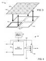
- a generic non-volatile service layer 134 operated in accordance with various embodiments of the present inventionis displayed in FIG. 3 .
- the service layer 134can be configured as a testing layer 136 .
- an array of unit test structures (UTS) 138is included in the testing layer 136 .
- the UTS 138are programmable to test host functions 140 with a testing pattern stored in a non-volatile memory.
- the host functions 140are coupled to a host layer 142 .
- host functions 140can be included in the host layer 142 .
- a selected host function 140can have a test wrapper 144 at least partially surrounding it to isolate the testing of a single function 140 .
- several test wrappers 144can be implemented on various host functions 140 to be tested simultaneously or in succession.
- a configuration input 148can be configured to provide configuration data to the test resources 150 .
- the test resources 150can include one, or many, UTS 138 or an alternative test component to examine the operation of the host layer 142 .
- the test resources 150can be configured to perform a variety of combinational or sequential logic operations which can be programmed by the configuration data.
- an input register 152provides data to the test resources 150 .
- the functionality of the test resources 150can be implemented by various testing patterns that can be stored in the memory element 154 that can comprise spin torque random access memory (STRAM), resistive random access memory (RRAM), or phase change random access memory (PCRAM).
- STRAMspin torque random access memory
- RRAMresistive random access memory
- PCRAMphase change random access memory
- the configuration datais routed to a multiplexer 156 that sends output data 158 .
- the multiplexercan also be configured to receive output test signals 160 from the test resources 150 .
- various UTS 138can be inputted to the multiplexer 156 to provide more accurate output data 158 .
- the multiplexer 156can be configured to receive a single, or numerous inputs.
- the test resources 150can be configured to be a single type of resource, such as a sensor, or a variety of types of resources to work simultaneously or in succession to provide test output signals 160 .
- a performance layer 164is configured with an array of memory cells 166 .
- the memory cells 166can comprise various volatile and non-volatile memories such as, but not limited to STRAM, RRAM, PCRAM, dynamic random access memory (DRAM), or static random access memory (SRAM).
- the performance layer 164is configured to communicate with a look-up table 168 positioned on the host layer 142 . It should be noted that an array of look-up tables 168 can be implemented on the host layer 142 and capable of communicating with the memory cells 166 of the performance layer 164 . Further, the array of memory cells 166 can be configured to operate in a manner similar to a field programmable gate array (FPGA).
- FPGAfield programmable gate array
- FIG. 6generally illustrates control circuitry 170 operated in accordance with various embodiments of the present invention.
- a plurality of inputs 172is shown sending signals to the look-up table 168 of FIG. 5 .
- a memory element 174is connected to the look-up table 168 and allows for dynamically configuring the table. It should be noted that the memory element 174 can comprise various memories including, but not limited to, STRAM, RRAM, PCRAM, DRAM, and SRAM.
- the look-up table 168sends a table output 176 to a delay flip flop (DFF) 178 as well as a multiplexer 180 .
- the DFF 178has an input clock signal 182 controlling the operation of the flip flop 178 .
- the multiplexer 180sends a multiplexer output 184 to a host (not shown).
- FIG. 7shows a generic non-volatile service layer 186 operated in accordance with various embodiments of the present invention.
- a performance layer 164is configured to comprise various security components 188 .
- the security components 188can include, but are not limited to, a key, identification, handler, and configuration file.
- the security components 188are configured to communicate with an integrated circuit 190 implemented on the host layer 142 .
- the communication between the security components 188 and the integrated circuit 190can be configured to determine that the proper user is accessing the integrated circuit 190 . Further, the security components 188 can restrict access to the integrated circuit to only predetermined users.
- the security components 188can comprise a variety of data storage arrays. When the input key matches the device-specific key under certain algorithms, the data will be written into a predetermined storage component to allow full functionality of the performance layer 164 .
- FIG. 8generally illustrates a generic non-volatile service layer 192 operated in accordance with various embodiments of the present invention.
- a performance layer 164is configured to include at least a configuration region 194 that communicates with routing matrix 196 coupled to the host layer 142 , and integrated circuit 190 .
- the configuration region 194allows for the rerouting of circuitry such as, but not limited to, decoder address or redundant components.
- the inputs of such a routing matrixcan be stored in the performance layer 164 with programmability and reconfigured to correspond to redundancy requirements of the host layer 142 .
- a printed circuit board 200is generally illustrated employing a package 202 constructed in accordance with various embodiments of the present invention.
- the generic non-volatile service layer 134can be implemented in an integrated circuit that is installed on a printed circuit board 200 .
- the integrated circuitcan be a three-dimensional chip package 202 .
- the generic non-volatile service layer 134is configured to test an integrated circuit and subsequently reconfigured to a performance function such as, but not limited to, FPGA, security protocol, or redundancy correction as shown in FIGS. 5 , 7 , and 8 .
- the installation of a three-dimensional packageeliminates the need for connection pathways on the printed circuit board 200 and creates a blank area 204 where no electrical connections are present.
- the blank area 204surrounds the primary area of circuit board interconnect savings that leads to greater circuit board 200 performance due in part to reduced noise.
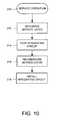
- FIG. 10displays a flow diagram of a service operation 210 performed in accordance with the various embodiments of the present invention.
- the service operation 210initially integrates the generic non-volatile service layer 134 to a host layer 142 of a three dimensional integrated circuit at step 212 .
- the service layer 134is tested with a testing pattern stored in non-volatile memory to ensure quality and reliability of the integrated circuit.
- the service layer 134is reconfigured to carry out a performance function in step 216 .
- the performance functioncan be, but is not limited to, a FPGA, security protocol, or redundancy correction.
- the performance function of the service layer 134is a permanent function of the integrated circuit.
- the integrated circuitis installed in an electronic device that can be, but is not limited to, a printed circuit board such as 200 of FIG. 9 .
- the various embodiments illustrated hereinprovide advantages in both electronic device efficiency and complexity.
- the use of tested and repaired known good die in conjunction with single function chips in a packageincreases the performance of the electrical device while reducing the noise associated with conventional chip integration.
- the various embodiments discussed hereinhave numerous potential applications and are not limited to a certain field of electronic media or type of data storage devices.
Landscapes
- Engineering & Computer Science (AREA)
- Computer Hardware Design (AREA)
- Physics & Mathematics (AREA)
- Theoretical Computer Science (AREA)
- Evolutionary Computation (AREA)
- Geometry (AREA)
- General Engineering & Computer Science (AREA)
- General Physics & Mathematics (AREA)
- Semiconductor Integrated Circuits (AREA)
- Tests Of Electronic Circuits (AREA)
Abstract
Description
Claims (16)
Priority Applications (1)
| Application Number | Priority Date | Filing Date | Title |
|---|---|---|---|
| US12/252,564US7966581B2 (en) | 2008-10-16 | 2008-10-16 | Generic non-volatile service layer |
Applications Claiming Priority (1)
| Application Number | Priority Date | Filing Date | Title |
|---|---|---|---|
| US12/252,564US7966581B2 (en) | 2008-10-16 | 2008-10-16 | Generic non-volatile service layer |
Publications (2)
| Publication Number | Publication Date |
|---|---|
| US20100100857A1 US20100100857A1 (en) | 2010-04-22 |
| US7966581B2true US7966581B2 (en) | 2011-06-21 |
Family
ID=42109621
Family Applications (1)
| Application Number | Title | Priority Date | Filing Date |
|---|---|---|---|
| US12/252,564Expired - Fee RelatedUS7966581B2 (en) | 2008-10-16 | 2008-10-16 | Generic non-volatile service layer |
Country Status (1)
| Country | Link |
|---|---|
| US (1) | US7966581B2 (en) |
Families Citing this family (5)
| Publication number | Priority date | Publication date | Assignee | Title |
|---|---|---|---|---|
| US8269204B2 (en) | 2009-07-02 | 2012-09-18 | Actel Corporation | Back to back resistive random access memory cells |
| US10270451B2 (en) | 2015-12-17 | 2019-04-23 | Microsemi SoC Corporation | Low leakage ReRAM FPGA configuration cell |
| US10147485B2 (en) | 2016-09-29 | 2018-12-04 | Microsemi Soc Corp. | Circuits and methods for preventing over-programming of ReRAM-based memory cells |
| WO2018106450A1 (en) | 2016-12-09 | 2018-06-14 | Microsemi Soc Corp. | Resistive random access memory cell |
| US10522224B2 (en) | 2017-08-11 | 2019-12-31 | Microsemi Soc Corp. | Circuitry and methods for programming resistive random access memory devices |
Citations (21)
| Publication number | Priority date | Publication date | Assignee | Title |
|---|---|---|---|---|
| US6551857B2 (en)* | 1997-04-04 | 2003-04-22 | Elm Technology Corporation | Three dimensional structure integrated circuits |
| US20050023656A1 (en)* | 2002-08-08 | 2005-02-03 | Leedy Glenn J. | Vertical system integration |
| US20050066226A1 (en)* | 2003-09-23 | 2005-03-24 | Adams R. Dean | Redundant memory self-test |
| US20050278666A1 (en)* | 2003-09-15 | 2005-12-15 | Diamond Michael B | System and method for testing and configuring semiconductor functional circuits |
| US7064018B2 (en) | 2002-07-08 | 2006-06-20 | Viciciv Technology | Methods for fabricating three dimensional integrated circuits |
| US20070080448A1 (en) | 2005-10-11 | 2007-04-12 | International Business Machines Corporation | Method and structure for optimizing yield of 3-d chip manufacture |
| US7219271B2 (en)* | 2001-12-14 | 2007-05-15 | Sandisk 3D Llc | Memory device and method for redundancy/self-repair |
| US7312109B2 (en) | 2002-07-08 | 2007-12-25 | Viciciv, Inc. | Methods for fabricating fuse programmable three dimensional integrated circuits |
| US7334159B1 (en)* | 2003-09-29 | 2008-02-19 | Rockwell Automation Technologies, Inc. | Self-testing RAM system and method |
| US7379327B2 (en)* | 2006-06-26 | 2008-05-27 | Grandis, Inc. | Current driven switching of magnetic storage cells utilizing spin transfer and magnetic memories using such cells having enhanced read and write margins |
| US20080163139A1 (en) | 2006-12-29 | 2008-07-03 | Cadence Design Systems, Inc. | Method, system, and computer program product for preparing multiple layers of semiconductor substrates for electronic designs |
| US7412343B2 (en)* | 2002-07-01 | 2008-08-12 | University Of North Carolina At Charlotte | Methods for delay-fault testing in field-programmable gate arrays |
| US20080229269A1 (en)* | 2007-03-12 | 2008-09-18 | International Business Machines Corporation | Design structure for integrating nonvolatile memory capability within sram devices |
| US7463062B2 (en)* | 2004-07-27 | 2008-12-09 | Easic Corporation | Structured integrated circuit device |
| US20090063916A1 (en)* | 2007-08-28 | 2009-03-05 | Thomas Vogelsang | Method for self-test and self-repair in a multi-chip package environment |
| US20090106716A1 (en)* | 2007-10-18 | 2009-04-23 | Virage Logic Corporation | Various methods and apparatuses for memory modeling using a structural primitive verification for memory compilers |
| US20090129186A1 (en)* | 2007-11-20 | 2009-05-21 | Josef Schnell | Self-diagnostic scheme for detecting errors |
| US20090300441A1 (en)* | 2008-05-27 | 2009-12-03 | Alexandre Andreev | Address controlling in the mbist chain architecture |
| US20100061207A1 (en)* | 2008-09-09 | 2010-03-11 | Seagate Technology Llc | Data storage device including self-test features |
| US20100083037A1 (en)* | 2008-09-30 | 2010-04-01 | Infineon Technologies Ag | Memory repair |
| US7750421B2 (en)* | 2007-07-23 | 2010-07-06 | Magic Technologies, Inc. | High performance MTJ element for STT-RAM and method for making the same |
- 2008
- 2008-10-16USUS12/252,564patent/US7966581B2/ennot_activeExpired - Fee Related
Patent Citations (26)
| Publication number | Priority date | Publication date | Assignee | Title |
|---|---|---|---|---|
| US6551857B2 (en)* | 1997-04-04 | 2003-04-22 | Elm Technology Corporation | Three dimensional structure integrated circuits |
| US7219271B2 (en)* | 2001-12-14 | 2007-05-15 | Sandisk 3D Llc | Memory device and method for redundancy/self-repair |
| US7412343B2 (en)* | 2002-07-01 | 2008-08-12 | University Of North Carolina At Charlotte | Methods for delay-fault testing in field-programmable gate arrays |
| US7312109B2 (en) | 2002-07-08 | 2007-12-25 | Viciciv, Inc. | Methods for fabricating fuse programmable three dimensional integrated circuits |
| US7064018B2 (en) | 2002-07-08 | 2006-06-20 | Viciciv Technology | Methods for fabricating three dimensional integrated circuits |
| US7402897B2 (en)* | 2002-08-08 | 2008-07-22 | Elm Technology Corporation | Vertical system integration |
| US20050023656A1 (en)* | 2002-08-08 | 2005-02-03 | Leedy Glenn J. | Vertical system integration |
| US20090194768A1 (en)* | 2002-08-08 | 2009-08-06 | Leedy Glenn J | Vertical system integration |
| US20080284611A1 (en)* | 2002-08-08 | 2008-11-20 | Elm Technology Corporation | Vertical system integration |
| US20050278666A1 (en)* | 2003-09-15 | 2005-12-15 | Diamond Michael B | System and method for testing and configuring semiconductor functional circuits |
| US20050066226A1 (en)* | 2003-09-23 | 2005-03-24 | Adams R. Dean | Redundant memory self-test |
| US7334159B1 (en)* | 2003-09-29 | 2008-02-19 | Rockwell Automation Technologies, Inc. | Self-testing RAM system and method |
| US7463062B2 (en)* | 2004-07-27 | 2008-12-09 | Easic Corporation | Structured integrated circuit device |
| US20080142959A1 (en) | 2005-10-11 | 2008-06-19 | Demulder Edward M | Method and Structure for Optimizing Yield of 3-D Chip Manufacture |
| US20070080448A1 (en) | 2005-10-11 | 2007-04-12 | International Business Machines Corporation | Method and structure for optimizing yield of 3-d chip manufacture |
| US7379327B2 (en)* | 2006-06-26 | 2008-05-27 | Grandis, Inc. | Current driven switching of magnetic storage cells utilizing spin transfer and magnetic memories using such cells having enhanced read and write margins |
| US20080163139A1 (en) | 2006-12-29 | 2008-07-03 | Cadence Design Systems, Inc. | Method, system, and computer program product for preparing multiple layers of semiconductor substrates for electronic designs |
| US20080229269A1 (en)* | 2007-03-12 | 2008-09-18 | International Business Machines Corporation | Design structure for integrating nonvolatile memory capability within sram devices |
| US7750421B2 (en)* | 2007-07-23 | 2010-07-06 | Magic Technologies, Inc. | High performance MTJ element for STT-RAM and method for making the same |
| US20090063916A1 (en)* | 2007-08-28 | 2009-03-05 | Thomas Vogelsang | Method for self-test and self-repair in a multi-chip package environment |
| US20090106716A1 (en)* | 2007-10-18 | 2009-04-23 | Virage Logic Corporation | Various methods and apparatuses for memory modeling using a structural primitive verification for memory compilers |
| US20090129186A1 (en)* | 2007-11-20 | 2009-05-21 | Josef Schnell | Self-diagnostic scheme for detecting errors |
| US7694196B2 (en)* | 2007-11-20 | 2010-04-06 | Qimonda North America Corp. | Self-diagnostic scheme for detecting errors |
| US20090300441A1 (en)* | 2008-05-27 | 2009-12-03 | Alexandre Andreev | Address controlling in the mbist chain architecture |
| US20100061207A1 (en)* | 2008-09-09 | 2010-03-11 | Seagate Technology Llc | Data storage device including self-test features |
| US20100083037A1 (en)* | 2008-09-30 | 2010-04-01 | Infineon Technologies Ag | Memory repair |
Non-Patent Citations (2)
| Title |
|---|
| Jing Li, "An Alternate Design Paradigm using Scaled Low Temperature Poly-Silicon Thin Film Transistor (LTPS TFT) for Low Power and Low-Cost Applications," Sep. 2007, 1-90, Purdue University, US. |
| Weisheng Zhao, Eric Belhaire, Bernard Dieny, Guillaume Prenat and Claude Chappert, "TAS-MRAM based Non-volatile FPGA logic circuit," IEEE, 2007, 1-8. |
Also Published As
| Publication number | Publication date |
|---|---|
| US20100100857A1 (en) | 2010-04-22 |
Similar Documents
| Publication | Publication Date | Title |
|---|---|---|
| US9300298B2 (en) | Programmable logic circuit using three-dimensional stacking techniques | |
| EP3129987B1 (en) | Soft post package repair of memory devices | |
| US9972611B2 (en) | Stacked semiconductor package having fault detection and a method for identifying a fault in a stacked package | |
| CN107148650B (en) | Apparatus and method for performing post-package trim | |
| US8380927B2 (en) | Upgradable system with reconfigurable interconnect | |
| TWI590250B (en) | Apparatus and method for configuring input/output of memory for mixed memory modules | |
| US8648339B2 (en) | Semiconductor device including first semiconductor chip including first pads connected to first terminals, and second semiconductor chip including second pads connected to second terminals | |
| US7966581B2 (en) | Generic non-volatile service layer | |
| KR20130033456A (en) | An integrated memory core and memory interface circuit | |
| US11113222B2 (en) | NAND switch | |
| JP3657498B2 (en) | Semiconductor memory device and reading method in test mode thereof | |
| KR20170036884A (en) | Repair circuit, semiconductor apparatus and semiconductor system using the same | |
| US20160246712A1 (en) | Indirection data structures implemented as reconfigurable hardware | |
| US8081504B2 (en) | Computer memory device with status register | |
| CN102024489A (en) | Semiconductor memory device and multilayered chip semiconductor device | |
| TWI451428B (en) | Programmable loading test system with advance features for completed memory system | |
| CN117912527A (en) | Multimodal memory device and system | |
| JP3588075B2 (en) | Integrated circuit and test method for the integrated circuit | |
| US7936057B2 (en) | High bandwidth package | |
| KR20190069782A (en) | Stacked Memory Apparatus Using Base Die Spare Cell and Repair Method Thereof | |
| US12243606B2 (en) | Semiconductor device, memory system and method of controlling semiconductor device thereof | |
| US6909624B2 (en) | Semiconductor memory device and test method thereof | |
| US20100177562A1 (en) | Computer memory device with multiple interfaces | |
| US9529744B2 (en) | Interface between multiple controllers | |
| JP2008077635A (en) | Memory system |
Legal Events
| Date | Code | Title | Description |
|---|---|---|---|
| AS | Assignment | Owner name:SEAGATE TECHNOLOGY LLC,CALIFORNIA Free format text:ASSIGNMENT OF ASSIGNORS INTEREST;ASSIGNORS:CHEN, YIRAN;SETIADI, DADI;LI, HAI;AND OTHERS;REEL/FRAME:021690/0426 Effective date:20081014 Owner name:SEAGATE TECHNOLOGY LLC, CALIFORNIA Free format text:ASSIGNMENT OF ASSIGNORS INTEREST;ASSIGNORS:CHEN, YIRAN;SETIADI, DADI;LI, HAI;AND OTHERS;REEL/FRAME:021690/0426 Effective date:20081014 | |
| AS | Assignment | Owner name:WELLS FARGO BANK, NATIONAL ASSOCIATION, AS COLLATERAL AGENT AND SECOND PRIORITY REPRESENTATIVE, CALIFORNIA Free format text:SECURITY AGREEMENT;ASSIGNORS:MAXTOR CORPORATION;SEAGATE TECHNOLOGY LLC;SEAGATE TECHNOLOGY INTERNATIONAL;REEL/FRAME:022757/0017 Effective date:20090507 Owner name:JPMORGAN CHASE BANK, N.A., AS ADMINISTRATIVE AGENT AND FIRST PRIORITY REPRESENTATIVE, NEW YORK Free format text:SECURITY AGREEMENT;ASSIGNORS:MAXTOR CORPORATION;SEAGATE TECHNOLOGY LLC;SEAGATE TECHNOLOGY INTERNATIONAL;REEL/FRAME:022757/0017 Effective date:20090507 Owner name:JPMORGAN CHASE BANK, N.A., AS ADMINISTRATIVE AGENT Free format text:SECURITY AGREEMENT;ASSIGNORS:MAXTOR CORPORATION;SEAGATE TECHNOLOGY LLC;SEAGATE TECHNOLOGY INTERNATIONAL;REEL/FRAME:022757/0017 Effective date:20090507 Owner name:WELLS FARGO BANK, NATIONAL ASSOCIATION, AS COLLATE Free format text:SECURITY AGREEMENT;ASSIGNORS:MAXTOR CORPORATION;SEAGATE TECHNOLOGY LLC;SEAGATE TECHNOLOGY INTERNATIONAL;REEL/FRAME:022757/0017 Effective date:20090507 | |
| AS | Assignment | Owner name:SEAGATE TECHNOLOGY INTERNATIONAL, CALIFORNIA Free format text:RELEASE;ASSIGNOR:JPMORGAN CHASE BANK, N.A., AS ADMINISTRATIVE AGENT;REEL/FRAME:025662/0001 Effective date:20110114 Owner name:SEAGATE TECHNOLOGY LLC, CALIFORNIA Free format text:RELEASE;ASSIGNOR:JPMORGAN CHASE BANK, N.A., AS ADMINISTRATIVE AGENT;REEL/FRAME:025662/0001 Effective date:20110114 Owner name:MAXTOR CORPORATION, CALIFORNIA Free format text:RELEASE;ASSIGNOR:JPMORGAN CHASE BANK, N.A., AS ADMINISTRATIVE AGENT;REEL/FRAME:025662/0001 Effective date:20110114 Owner name:SEAGATE TECHNOLOGY HDD HOLDINGS, CALIFORNIA Free format text:RELEASE;ASSIGNOR:JPMORGAN CHASE BANK, N.A., AS ADMINISTRATIVE AGENT;REEL/FRAME:025662/0001 Effective date:20110114 | |
| AS | Assignment | Owner name:THE BANK OF NOVA SCOTIA, AS ADMINISTRATIVE AGENT, CANADA Free format text:SECURITY AGREEMENT;ASSIGNOR:SEAGATE TECHNOLOGY LLC;REEL/FRAME:026010/0350 Effective date:20110118 Owner name:THE BANK OF NOVA SCOTIA, AS ADMINISTRATIVE AGENT, Free format text:SECURITY AGREEMENT;ASSIGNOR:SEAGATE TECHNOLOGY LLC;REEL/FRAME:026010/0350 Effective date:20110118 | |
| STCF | Information on status: patent grant | Free format text:PATENTED CASE | |
| AS | Assignment | Owner name:SEAGATE TECHNOLOGY LLC, CALIFORNIA Free format text:TERMINATION AND RELEASE OF SECURITY INTEREST IN PATENT RIGHTS;ASSIGNOR:WELLS FARGO BANK, NATIONAL ASSOCIATION, AS COLLATERAL AGENT AND SECOND PRIORITY REPRESENTATIVE;REEL/FRAME:030833/0001 Effective date:20130312 Owner name:SEAGATE TECHNOLOGY INTERNATIONAL, CAYMAN ISLANDS Free format text:TERMINATION AND RELEASE OF SECURITY INTEREST IN PATENT RIGHTS;ASSIGNOR:WELLS FARGO BANK, NATIONAL ASSOCIATION, AS COLLATERAL AGENT AND SECOND PRIORITY REPRESENTATIVE;REEL/FRAME:030833/0001 Effective date:20130312 Owner name:EVAULT INC. (F/K/A I365 INC.), CALIFORNIA Free format text:TERMINATION AND RELEASE OF SECURITY INTEREST IN PATENT RIGHTS;ASSIGNOR:WELLS FARGO BANK, NATIONAL ASSOCIATION, AS COLLATERAL AGENT AND SECOND PRIORITY REPRESENTATIVE;REEL/FRAME:030833/0001 Effective date:20130312 Owner name:SEAGATE TECHNOLOGY US HOLDINGS, INC., CALIFORNIA Free format text:TERMINATION AND RELEASE OF SECURITY INTEREST IN PATENT RIGHTS;ASSIGNOR:WELLS FARGO BANK, NATIONAL ASSOCIATION, AS COLLATERAL AGENT AND SECOND PRIORITY REPRESENTATIVE;REEL/FRAME:030833/0001 Effective date:20130312 | |
| FPAY | Fee payment | Year of fee payment:4 | |
| FEPP | Fee payment procedure | Free format text:MAINTENANCE FEE REMINDER MAILED (ORIGINAL EVENT CODE: REM.); ENTITY STATUS OF PATENT OWNER: LARGE ENTITY | |
| LAPS | Lapse for failure to pay maintenance fees | Free format text:PATENT EXPIRED FOR FAILURE TO PAY MAINTENANCE FEES (ORIGINAL EVENT CODE: EXP.); ENTITY STATUS OF PATENT OWNER: LARGE ENTITY | |
| STCH | Information on status: patent discontinuation | Free format text:PATENT EXPIRED DUE TO NONPAYMENT OF MAINTENANCE FEES UNDER 37 CFR 1.362 | |
| FP | Lapsed due to failure to pay maintenance fee | Effective date:20190621 | |
| AS | Assignment | Owner name:SEAGATE TECHNOLOGY PUBLIC LIMITED COMPANY, CALIFORNIA Free format text:RELEASE BY SECURED PARTY;ASSIGNOR:THE BANK OF NOVA SCOTIA;REEL/FRAME:072193/0001 Effective date:20250303 Owner name:SEAGATE TECHNOLOGY, CALIFORNIA Free format text:RELEASE BY SECURED PARTY;ASSIGNOR:THE BANK OF NOVA SCOTIA;REEL/FRAME:072193/0001 Effective date:20250303 Owner name:SEAGATE TECHNOLOGY HDD HOLDINGS, CALIFORNIA Free format text:RELEASE BY SECURED PARTY;ASSIGNOR:THE BANK OF NOVA SCOTIA;REEL/FRAME:072193/0001 Effective date:20250303 Owner name:I365 INC., CALIFORNIA Free format text:RELEASE BY SECURED PARTY;ASSIGNOR:THE BANK OF NOVA SCOTIA;REEL/FRAME:072193/0001 Effective date:20250303 Owner name:SEAGATE TECHNOLOGY LLC, CALIFORNIA Free format text:RELEASE BY SECURED PARTY;ASSIGNOR:THE BANK OF NOVA SCOTIA;REEL/FRAME:072193/0001 Effective date:20250303 Owner name:SEAGATE TECHNOLOGY INTERNATIONAL, CAYMAN ISLANDS Free format text:RELEASE BY SECURED PARTY;ASSIGNOR:THE BANK OF NOVA SCOTIA;REEL/FRAME:072193/0001 Effective date:20250303 Owner name:SEAGATE HDD CAYMAN, CAYMAN ISLANDS Free format text:RELEASE BY SECURED PARTY;ASSIGNOR:THE BANK OF NOVA SCOTIA;REEL/FRAME:072193/0001 Effective date:20250303 Owner name:SEAGATE TECHNOLOGY (US) HOLDINGS, INC., CALIFORNIA Free format text:RELEASE BY SECURED PARTY;ASSIGNOR:THE BANK OF NOVA SCOTIA;REEL/FRAME:072193/0001 Effective date:20250303 |