US7966481B2 - Computer system and method for executing port communications without interrupting the receiving computer - Google Patents
Computer system and method for executing port communications without interrupting the receiving computerDownload PDFInfo
- Publication number
- US7966481B2 US7966481B2US11/653,187US65318707AUS7966481B2US 7966481 B2US7966481 B2US 7966481B2US 65318707 AUS65318707 AUS 65318707AUS 7966481 B2US7966481 B2US 7966481B2
- Authority
- US
- United States
- Prior art keywords
- program
- computer
- processor
- executing
- instructions
- Prior art date
- Legal status (The legal status is an assumption and is not a legal conclusion. Google has not performed a legal analysis and makes no representation as to the accuracy of the status listed.)
- Expired - Fee Related, expires
Links
Images


Classifications
- G—PHYSICS
- G06—COMPUTING OR CALCULATING; COUNTING
- G06F—ELECTRIC DIGITAL DATA PROCESSING
- G06F1/00—Details not covered by groups G06F3/00 - G06F13/00 and G06F21/00
- G06F1/26—Power supply means, e.g. regulation thereof
- G06F1/32—Means for saving power
Definitions
- the present inventionrelates to the field of computers and computer processors, and more particularly to a method and means for allowing a computer to execute instructions as they are received from an external source without first storing said instructions, and an associated method to facilitate communications between computers and the ability of a computer to use the available resources of another computer.
- the predominant current usage of the present inventive direct execution method and apparatusis in the combination of multiple computers on a single microchip, wherein operating efficiency is important not only because of the desire for increased operating speed but also because of the power savings and heat reduction that are a consequence of the greater efficiency.
- the use of multiple processorscreates a need for communication between the processors. Therefore, there is a significant portion of time spent in transferring instructions and data between processors. Each additional instruction that must be executed in order to accomplish this places an incremental delay in the process which, cumulatively, can be very significant.
- the conventional method for communicating instructions or data from one computer to anotherinvolves first storing the data or instruction in the receiving computer and then, subsequently calling it for execution (in the case of an instruction) or for operation thereon (in the case of data).
- I/Oinput/output
- a processorcan go about performing its assigned task and then, when an I/O port/device needs attention or the status changes, it sends an Interrupt Request (IRQ) to the processor.
- IRQInterrupt Request
- the processorOnce the processor receives an Interrupt Request, it will, for example, finish its current instruction, place a few things on the stack, and then execute the appropriate Interrupt Service Routine (ISR).
- ISRInterrupt Service Routine
- the processorreturns to where it left off.
- the processordoesn't have to waste time, looking to see if the I/O device is in need of attention, but rather the device will only service the interrupt when it needs attention.
- the use of interruptsis far less than desirable in many cases, since there can be a great deal of overhead associated with the use of interrupts. For example, each time an interrupt occurs, a computer may have to temporarily store certain data relating to the task it was previously trying to accomplish, then load data pertaining to the interrupt, and then reload the data necessary for the prior task once the interrupt is handled.
- Forth systemshave been able to have more than one “thread” of code executing at one time. This is often called a cooperative round-robin.
- the order in which the threads get a turn using the central processing unit (CPU)is fixed; for example, thread 4 always gets its turn after thread 3 and before thread 5 .
- Each threadis allowed to keep the CPU as long as it wants to, and then relinquish it voluntarily. The thread does this by calling the word PAUSE. Only a few data items need to be saved during a PAUSE function in order for the original task to be restored, as opposed to large contexts that need to be saved during an interrupt function.
- Each threadmay or may not have work to do. If task 4 has work to do and the task before it in the round-robin (task 3 ) calls PAUSE, then task 4 will wake up and work until it decides to PAUSE again. If task 4 has no work to do, it passes control on to task 5 . When a task calls a word which will perform an input/output function, and will therefore need to wait for the input/output to finish, a PAUSE is built into the input/output call.
- PAUSEThe predictability of PAUSE allows for very efficient code. Frequently, a Forth based cooperative round-robin can give every existing thread a turn at the CPU in less time than it would take a pre-emptive multitasker to decide who should get the CPU next. However, a particular task may tend to overwhelm or overtake the CPU.
- Another area of operating efficiencycan be found by minimizing leakage current in a computer system.
- leakage currentincreases as insulation layers become thinner.
- leakage powercould reach as high as 50% of the active power.
- One attempt to curb leakage currentcan be found by utilizing sleep transistors. Sleep transistors act like a switch by isolating or disconnecting the power supply and blocks of logic when they are not needed. This can reduce leakage power by a factor of 2-1000 times, as disclosed in an article entitled How to Provide a Power - Efficient Architecture , by Bob Crepps, published in Embedded.com, Jul. 24, 2006.
- CMOScomplementary metal-oxide semiconductor
- the sleep transistorshave to be carefully sized to decrease their voltage drop while they are on. Two gates that switch at different times can share a sleep transistor. However, this is not practical for large circuits. Algorithms are necessary to determine the best implementation of sleep transistors for large circuits.
- a computer processor arrayin which power usage and heat dissipation are minimized, and computing efficiency is maximized. This is realized in part by a computer processor array, in which processors, also called nodes or cores become inactive but alert when not in an operating mode.
- processorsalso called nodes or cores become inactive but alert when not in an operating mode.
- the inactive node or coreconsumes essentially no power while inactive, and becomes active when an adjacent node or pin attempts to communicate with it. After execution of an incoming task, the node will go back to an inactive state until another task is sent to the node.
- Array efficiencyis also realized when a core is currently executing code or instructions, and a neighboring core communicates to the executing core. Rather then interrupting the executing core as in a conventional computing system, cores can be programmed to occasionally pause to check for incoming messages. If an incoming message awaits, then the executing core can act on the incoming message after pausing, and then continue with its original task.
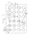
- FIG. 1is a diagrammatic view of a computer processor array, according to the present invention.
- FIG. 2is a detailed diagram showing a subset of the computer processors of FIG. 1 and a more detailed view of the interconnecting data buses of FIG. 1 ;
- FIG. 3is a block diagram depicting a general layout of one of the processors of FIGS. 1 and 2 ;
- FIG. 4is a diagrammatic representation of an instruction word according to the present inventive application.
- FIG. 5is a flow diagram depicting an example of a micro-loop according to the present invention.
- FIG. 6is a flow diagram depicting an example of the inventive method for executing instructions from a port
- FIG. 7is a flow diagram depicting an example of the inventive improved method for alerting a processor
- FIG. 8is a flow diagram depicting a method for awakening a processor and sending input to an executing processor
- FIG. 9is a diagrammatic view of the processor array of FIG. 1 with the processor or node identification and sharing ports with adjacent processors utilizing mirroring;
- FIG. 9 ais a partial view of FIG. 9 with additional port detail
- FIG. 10is a partial view of an I/O register
- FIG. 11is a flow diagram depicting a worker mode loop
- FIG. 12is a flow diagram depicting an executing processor with a PAUSE routine.
- processorsalso called computers, nodes, or cores
- processorsalso called computers, nodes, or cores
- processorsthat operate in a mode referred to as “asleep but alert” or “inactive but alert” which both refer to a mode of operation in which the processor's functions have been temporarily suspended, halted, or ceased where essentially no power is being utilized.
- the processoris alert or in a state of readiness to immediately begin processing functions when instructed to do so.
- the inactive processorreceives processing instructions, it is referred to as “being awakened” or “becoming activated.”
- a mode for carrying out the inventionis given by an array of individual computer processors.
- the arrayis depicted in a diagrammatic view in FIG. 1 and is designated therein by the general reference character 10 .
- the processor array 10has a plurality (twenty four in the example shown) of computer processors 12 (sometimes also referred to as “cores” or “nodes” in the example of an array). In the example shown, all of the processors 12 are located on a single die 14 . According to the present invention, each of the processors 12 is a generally independently functioning processor, as will be discussed in more detail hereinafter.
- the processors 12are interconnected by a plurality (the quantities of which will be discussed in more detail hereinafter) of interconnecting data buses 16 .
- the data buses 16are bidirectional asynchronous high speed parallel data buses, although it is within the scope of the invention that other interconnecting means might be employed for the purpose.
- the array 10not only is data communication between the processors 12 asynchronous, but the individual processors 12 also operate in an internally asynchronous mode. This has been found by the inventor to provide important advantages. For example, since a clock signal does not have to be distributed throughout the processor array 10 , a great deal of power is saved. Furthermore, not having to distribute a clock signal eliminates many timing problems that could limit the size of the array 10 or cause other known difficulties. Also, the fact that the individual processors operate asynchronously saves a great deal of power, since each processor will use essentially no power when it is not executing instructions because there is no clock running therein.
- Such additional componentsinclude, but are not limited to power buses, external connection pads, and other such common aspects of a microprocessor chip.
- Processor 12 eis an example of one of the processors 12 that is not on the periphery of the array 10 . That is, processor 12 e has four orthogonally adjacent processors 12 a , 12 b , 12 c and 12 d , although it is within the scope of this invention that more than four adjacent processors could be utilized. This grouping of processors 12 a through 12 e will be used, by way of example, hereinafter in relation to a more detailed discussion of the communications between the processors 12 of the array 10 . As can be seen in the view of FIG. 1 , interior processors such as processor 12 e will have at lease four other processors 12 with which they can directly communicate via the buses 16 .
- processors 12 on the periphery of the array 10will be in direct communication with only three or, in the case of the corner processors 12 , only two other of the processors 12 .
- FIG. 2is a more detailed view of a portion of FIG. 1 showing only some of the processors 12 and, in particular, processors 12 a through 12 e , inclusive.
- the view of FIG. 2also reveals that the data buses 16 each have a read line 18 , a write line 20 and a plurality (eighteen, in this example) of data lines 22 .
- the data lines 22are capable of transferring all the bits of one eighteen-bit instruction word simultaneously in parallel.
- some of the processors 12are mirror images of adjacent processors. However, whether the processors 12 are all oriented identically or as mirror images of adjacent processors is not a limiting aspect of this presently described invention.
- a processor 12such as the processor 12 e can set high one, two, three or all four of its read lines 18 such that it is prepared to receive data from the respective one, two, three or all four adjacent processors 12 .
- a processor 12it is also possible for a processor 12 to set one, two, three or all four of its write lines 20 high.
- the receiving processormay try to set the write line 20 low slightly before the sending processor 12 releases (stops pulling high) its write line 20 . In such an instance, as soon as the sending processor 12 releases its write line 20 , the write line 20 will be pulled low by the receiving computer 12 e . It is important to note that when the write line 20 of the sending processor 12 goes high, the data or code is already transferred; therefore, the receiving processor ( 12 e in this instance) merely needs to latch the data/code for an essentially instantaneous response.
- processor 12 ewould set the write line 20 between processor 12 e and processor 12 a to high. If the read line 18 between processor 12 e and processor 12 a has then not already been set to high by processor 12 a , then processor 12 e will simply wait until processor 12 a does set that read line 20 high. When both of a corresponding pair of write line 18 and read line 20 are set high, then the data awaiting to be transferred on the data lines 22 is transferred.
- the receiving processor 12sets both the read line 18 and the write line 20 between the two processors ( 12 e and 12 a in this example) to low as soon as the sending processor 12 e releases the write line 18 .
- a processor 12such as the processor 12 e has set one of its write lines 20 high in anticipation of writing it will simply wait, using essentially no power, until the data is “requested”, as described above, from the appropriate adjacent processor 12 , unless the processor 12 to which the data is to be sent has already set its read line 18 high, in which case the data is transmitted immediately. Similarly, whenever a processor 12 has set one or more of its read lines 18 to high in anticipation of reading, it will simply wait, using essentially no power, until the write line 20 connected to a selected processor 12 goes high to transfer an instruction word between the two processors 12 .
- processors 12there may be several potential means and/or methods to cause the processors 12 to function as described.
- the processors 12so behave simply because they are operating generally asynchronously internally (in addition to transferring data there-between in the asynchronous manner described). That is, instructions are generally completed sequentially. When either a write or read instruction occurs, there can be no further action until that instruction is completed (or, perhaps alternatively, until it is aborted, as by a “reset” or the like). There is no regular clock pulse, in the prior art sense.
- a pulseis generated to accomplish a next instruction only when the instruction being executed either is not a read or write type instruction (given that a read or write type instruction would require completion, often by another entity) or else when the read or write type operation is, in fact, completed.
- FIG. 3is a block diagram depicting the general layout of an example of one of the processors 12 of FIGS. 1 and 2 .
- each of the processors 12is a generally self contained computer having its own random access memory (RAM) 24 and read only memory (ROM) 26 .
- RAMrandom access memory
- ROMread only memory
- the processors 12are also sometimes referred to as individual “nodes”, given that they are, in the present example, combined on a single chip.
- a return stack 28(including an R register 29 , discussed hereinafter), an instruction area 30 , an arithmetic logic unit (“ALU” or “processor”) 32 , a data stack 34 , a decode logic section 36 for decoding instructions, and a slot sequencer 42 .
- ALUarithmetic logic unit
- the processors 12are dual stack processors having the data stack 34 and the separate return stack 28 .
- FIG. 3also shows circular register arrays 28 a and 34 a for the return stack and data stack, respectively, along with the T register 44 and S register 46 of the data stack 34 .
- the processor 12has four communication ports 38 for communicating with adjacent processors 12 .
- the communication ports 38are tri-state drivers, having an off status, a receive status (for driving signals into the processor 12 ) and a send status (for driving signals out of the processor 12 ). If the particular processor 12 is not on the interior of the array ( FIG. 1 ) such as the example of processor 12 e , then one or more of the communication ports 38 will not be used in that particular processor, at least for the purposes described above. However, those communication ports 38 that do abut the edge of the die 14 can have additional circuitry, either designed into such processor 12 or else external to the processor 12 but associated therewith, to cause such communication port 38 to act as an external I/O port 39 ( FIG. 1 ).
- Examples of such external I/O ports 39include, but are not limited to, USB (universal serial bus) ports, RS232 serial bus ports, parallel communications ports, analog to digital and/or digital to analog conversion ports, and many other possible variations. No matter what type of additional or modified circuitry is employed for this purpose, according to the presently described embodiment of the invention, the method of operation of the “external” I/O ports 39 regarding the handling of instructions and/or data received there from will be alike to that described herein, in relation to the “internal” communication ports 38 .
- an “edge” processor 12 fis depicted with associated interface circuitry 80 (shown in block diagrammatic form) for communicating through an external I/O port 39 with an external device 82 .
- the instruction area 30includes a number of registers 40 including, in this example, an A register 40 a , a B register 40 b and a P register 40 c .
- the A register 40 ais a full eighteen-bit register
- the B register 40 b and the P register 40 care nine-bit registers.
- An I/O register 47(18 bit) is located between the memory (ROM 26 and RAM 24 ) and the communication ports 38 . The I/O register 47 will be disclosed in greater detail hereinafter.
- the present processor 12is implemented to execute native Forth language instructions.
- Forth wordsare constructed from the native processor instructions designed into the processor.
- the collection of Forth wordsis known as a “dictionary”.
- the processor 12reads eighteen bits at a time from RAM 24 , ROM 26 or directly from one of the data buses 16 ( FIG. 2 ).
- operand-less instructionssince in Forth most instructions (known as operand-less instructions) obtain their operands directly from the stacks 28 and 34 , they are generally only five bits in length, such that up to four instructions can be included in a single eighteen-bit instruction word, with the condition that the last instruction in the group is selected from a limited set of instructions that require only three bits.
- FIG. 4is a diagrammatic representation of an instruction word 48 .
- the instruction word 48can actually contain instructions, data, or some combination thereof.
- the instruction word 48consists of eighteen bits 50 . This being a binary computer, each of the bits 50 will be a ‘1’ or ‘0’.
- the eighteen-bit wide instruction word 48can contain up to four instructions 52 in four slots 54 called slot zero 54 a , slot one 54 b , slot two 54 c and slot three 54 d .
- the eighteen-bit instruction words 48are always read as a whole. Therefore, since there is always a potential of having up to four instructions in the instruction word 48 , a NOP (no operation) instruction is included in the instruction set of the processor 12 to provide for instances when using all of the available slots 54 might be unnecessary or even undesirable.
- the instruction area 30also has an 18 bit instruction register 30 a for storing the instruction word 48 that is presently being used, and an additional 5 bit opcode register 30 b for the instruction in the particular instruction word presently being executed.
- each instruction 52is set according to whether or not that instruction is either of a read or a write type of instruction, as opposed to that instruction being one that requires no input or output.
- the remaining bits 50 in the instruction 52provide the remainder of the particular opcode for that instruction.
- one or more of the bitsmay be used to indicate where data is to be read from, or written to, in that particular processor 12 .
- data to be writtenalways comes from the T register 44 (the top of the data stack 34 ); however data can be selectively read into either the T register 44 or else the instruction area 30 from where it can be executed.
- either data or instructionscan be communicated in the manner described herein and instructions can therefore, be executed directly from the data bus 16 .
- One or more of the bits 50will be used to indicate which of the ports 38 , if any, is to be set to read or write. This later operation is optionally accomplished by using one or more bits to designate a register 40 , such as the A register 40 a , the B register 40 b , or the like.
- the designated register 40will be preloaded with data having a bit corresponding to each of the ports 38 (and, also, any other potential entity with which the processor 12 may be attempting to communicate, such as memory (RAM 24 or ROM 26 ), an external communications port 39 , or the like.)
- each of four bits in the particular register 40can correspond to each of the up port 38 a , the right port 38 b , the left port 38 c or the down port 38 d . In such case, where there is a ‘1’ at any of those bit locations, communication will be set to proceed through the corresponding port 38 .
- a read opcodemight set more than one port 38 for communication in a single instruction.
- processor 12 eis attempting to write to processor 12 c , although the example is applicable to communication between any adjacent processors 12 .
- the selected write line 20in this example, the write line 20 between processors 12 e and 12 c
- the selected write line 20is set high; if the corresponding read line 18 is already high then data is immediately sent from the selected location through the selected communications port 38 .
- processor 12 ewill simply stop operation until the corresponding read line 18 does go high.
- both the read line 18 and the corresponding write line 20 between processors 12 e and 12 care high, then both lines 18 and 20 will be released by each of the respective processors 12 that is holding it high.
- the sending processor 12 ewill be holding the write line 18 high while the receiving processor 12 c will be holding the read line 20 high).
- the receiving processor 12 cwill pull both lines 18 and 20 low.
- the receiving processor 12 cmay attempt to pull the lines 18 and 20 low before the sending processor 12 e has released the write line 18 .
- any attempt to pull a line 18 or 20 lowwill not actually succeed until that line 18 or 20 is released by the processor 12 that is holding it high.
- processor 12 eattempts to write to processor 12 c first, or whether processor 12 c first attempts to read from processor 12 e .
- the operationcannot be completed until both processors 12 e and 12 c are ready and, whichever processor 12 e or 12 c is ready first, that first processor 12 simply “becomes inactive” until the other processor 12 e or 12 c completes the transfer.
- both the writing processor 12 e and the receiving processor 12 cbecome inactive when they execute the write and read instructions, respectively, but the last one to enter into the transaction reactivates nearly instantaneously when both the read line 18 and the write line 20 are high, whereas the first processor 12 to initiate the transaction can stay inactive nearly indefinitely until the second processor 12 is ready to complete the process.
- the inventor believes that a key feature for enabling efficient asynchronous communications between devicesis a type of acknowledge signal or condition.
- most communication between deviceshas been clocked and there is no direct way for a sending device to know that the receiving device has properly received the data.
- Methodssuch as checksum operations may have been used to attempt to insure that data is correctly received, but the sending device has no direct indication that the operation is completed.
- the present inventive methodprovides the necessary acknowledge condition that allows, or at least makes practical, asynchronous communications between the devices.
- the acknowledge conditionalso makes it possible for one or more of the devices to “become inactive” until the acknowledge condition occurs.
- An acknowledge conditioncould be communicated between the processors 12 by a separate signal being sent between the processors 12 (either over the interconnecting data bus 16 or over a separate signal line), and such an acknowledge signal would be within the scope of this aspect of the present invention.
- a separate signalbeing sent between the processors 12 (either over the interconnecting data bus 16 or over a separate signal line)
- such an acknowledge signalwould be within the scope of this aspect of the present invention.
- the method for acknowledgementdoes not require any additional signal, clock cycle, timing pulse, or any such resource beyond that described, to actually affect the communication.
- FIG. 5is a diagrammatic representation of a micro-loop 100 .
- the micro-loop 100not unlike other prior art loops, has a FOR instruction 102 and a NEXT instruction 104 . Since an instruction word 48 ( FIG. 4 ) contains as many as four instructions 52 , an instruction word 48 can include three operation instructions 106 within a single instruction word 48 .
- the operation instructions 106can be essentially any of the available instructions that a programmer might want to include in the micro-loop 100 .
- a typical example of a micro-loop 100 that might be transmitted from one processor 12 to anothermight be a set of instructions for reading from, or writing to the RAM 24 of the second processor 12 , such that the first processor 12 could “borrow” available RAM 24 capacity.
- the FOR instruction 102pushes a value onto the return stack 28 representing the number of iterations desired. That is, the value on the T register 44 at the top of the data stack 34 is pushed onto the R register 29 of the return stack 28 .
- the FOR instruction 102can be located in any slot 54 . Where the FOR instruction 102 is not located in slot three 54 d , then the remaining instructions 52 in that instruction word 48 will be executed before going on to the micro-loop 100 , which will generally be the next loaded instruction word 48 .
- the NEXT instruction 104 depicted in the view of FIG. 5is a particular type of NEXT instruction 104 . This is because it is located in slot three 54 d ( FIG. 4 ) According to this embodiment of the invention, it is assumed that all of the data in a particular instruction word 48 that follows an “ordinary” NEXT instruction (not shown) is an address (the address where the for/next loop begins).
- the opcode for the NEXT instruction 104is the same, no matter which of the four slots 54 it is in (with the obvious exception that the last two digits are assumed if it is in slot three 54 d , rather than being explicitly written, as discussed previously herein).
- the NEXT instruction 104 in slot three 54 dis a MICRO-NEXT instruction 104 a .
- the MICRO-NEXT instruction 104 auses the address of the first instruction 52 , located in slot zero 54 a of the same instruction word 48 in which it is located, as the address to which to return.
- the MICRO-NEXT instruction 104 aalso takes the value from the R register 29 (which was originally pushed there by the FOR instruction 102 ), decrements it by 1, and then returns it to the R register 29 .
- the MICRO-NEXT instructionWhen the value on the R register 29 reaches a predetermined value (such as zero), then the MICRO-NEXT instruction will load the next instruction word 48 and continue on as described previously herein. However, when the MICRO-NEXT instruction 104 a reads a value from the R register 29 that is greater than the predetermined value, it will resume operation at slot zero 54 a of its own instruction word 48 and execute the three instructions 52 located in slots zero through three, inclusive, thereof. That is, a MICRO-NEXT instruction 104 a will always, in this embodiment of the invention, execute three operation instructions 106 . Because, in some instances, it may not be desired to use all three potentially available instructions 52 , a “NOP” instruction is available to fill one or two of the slots 54 , as required.
- a predetermined valuesuch as zero
- micro-loops 100can be used entirely within a single processor 12 . Indeed, the entire set of available machine language instructions is available for use as the operation instructions 106 , and the application and use of micro-loops is limited only by the imagination of the programmer. However, when the ability to execute an entire micro-loop 100 within a single instruction word 48 is combined with the ability to allow a processor 12 to send the instruction word 48 to a neighbor processor 12 to execute the instructions 52 therein essentially directly from the data bus 16 , this provides a powerful tool for allowing a processor 12 to utilize the resources of its neighbors.
- the small micro-loop 100can be communicated between processors 12 , as described herein and it can be executed directly from the communications port 38 of the receiving processor 12 , just like any other set of instructions contained in an instruction word 48 , as described herein. While there are many uses for this sort of “micro-loop” 100 , a typical use would be where one processor 12 wants to store some data onto the memory of a neighbor processor 12 . It could, for example, first send an instruction to that neighbor processor telling it to store an incoming data word to a particular memory address, then increment that address, then repeat for a given number of iterations (the number of data words to be transmitted). To read the data back, the first processor would just instruct the second processor (the one used for storage here) to write the stored data back to the first processor, using a similar micro-loop.
- a processor 12can use an otherwise resting neighbor processor 12 for storage of excess data when the data storage need exceeds the relatively small capacity built into each individual processor 12 . While this example has been described in terms of data storage, the same technique can equally be used to allow a processor 12 to have its neighbor share its computational resources—by creating a micro-loop 100 that causes the other processor 12 to perform some operations, store the result, and repeat a given number of times. As can be appreciated, the number of ways in which this inventive micro-loop 100 structure can be used is nearly infinite.
- either data or instructionscan be communicated in the manner described herein and instructions can, therefore, be executed essentially directly from the data bus 16 . That is, there is no need to store instructions to RAM 24 and then recall them before execution. Instead, according to this aspect of the invention, an instruction word 48 that is received on a communications port 38 is not treated essentially differently than it would be were it recalled from RAM 24 or ROM 26 .
- the FETCH instructionuses the address on the A register 40 a to determine from where to fetch an 18 bit word. Of course, the program will have to have already provided for placing the correct address on the A register 40 a .
- the A register 40 ais an 18 bit register, such that there is a sufficient range of address data available that any of the potential sources from which a fetch can occur can be differentiated. That is, there is a range of addresses assigned to ROM, a different range of addresses assigned to RAM, and there are specific addresses for each of the ports 38 and for the external I/O port 39 .
- a FETCH instructionalways places the 18 bits that it fetches on the T register 44 . An important advantage exists here in that there are no instruction fetches inside the loop. Therefore, there is approximately a 30% increase in efficiency, with a corresponding decrease in power consumption.
- executable instructionsare temporarily stored in the instruction register 30 a .
- the processorwill automatically fetch the “next” instruction word 48 .
- the “program counter” or “pc”, herein called the P register 40 cis determined by the “program counter” or “pc”, herein called the P register 40 c .
- the P register 40 cis often automatically incremented, as is the case where a sequence of instruction words 48 is to be fetched from RAM 24 or ROM 26 .
- a JUMP or CALL instructionwill cause the P register 40 c to be loaded with the address designated by the data in the remainder of the presently loaded instruction word 48 after the JUMP or CALL instruction, rather than being incremented.
- the P register 40 cis then loaded with an address corresponding to one or more of the ports 38 , then the next instruction word 48 will be loaded into the instruction register 30 a from the ports 38 .
- the P register 40 calso does not increment when an instruction word 48 has just been retrieved from a port 38 into the instruction register 30 a . Rather, it will continue to retain that same port address until a specific JUMP or CALL instruction is executed to change the P register 40 c .
- processor 12once the processor 12 is told to look for its next instruction from a port 38 , it will continue to look for instructions from that same port 38 (or ports 38 ) until it is told to look elsewhere, such as back to the memory (RAM 24 or ROM 26 ) for its next instruction word 48 .
- the processor 12knows that the next eighteen bits fetched is to be placed in the instruction register 30 a when there are no more executable instructions left in the present instruction word 48 .
- there are no more executable instructions left in the present instruction word 48 after a JUMP or CALL instruction(or also after certain other instructions that will not be specifically discussed here) because, by definition, the remainder of the 18 bit instruction word following a JUMP or CALL instruction is dedicated to the address referred to by the JUMP or CALL instruction.
- Another way of stating thisis that the above described processes are unique in many ways, including but not limited to the fact that a JUMP or CALL instruction can, optionally, be to a port 38 , rather than to just a memory address, or the like.
- the processor 12can look for its next instruction from one port 38 or from any of a group of the ports 38 . Therefore, addresses are provided to correspond to various combinations of the ports 38 .
- a processoris told to FETCH an instruction from a group of ports 38 , then it will accept the first available instruction word 48 from any of the selected ports 38 . If no neighbor processor 12 has already attempted to write to any of those ports 38 , then the processor 12 in question will “become inactive”, as described in detail above, until a neighbor does write to the selected port 38 .
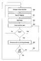
- FIG. 6is a flow diagram depicting an example of the above described direct execution method 120 .
- a “normal” flow of operationswill commence when, as discussed previously herein, there are no more executable instructions left in the instruction register 30 a .
- the processor 12will “fetch” another instruction word (note that the term “fetch” is used here in a general sense, in that an actual FETCH instruction is not used), as indicated by a “fetch word” operation 122 . That operation will be accomplished according to the address in the P register 40 c (as indicated by an “address” decision operation 124 in the flow diagram of FIG. 6 ).
- the next instruction word 48will be retrieved from the designated memory location in a “fetch from memory” operation 126 . If, on the other hand, the address in the P register 40 c is that of a port 38 or ports 38 (not a memory address), then the next instruction word 48 will be retrieved from the designated port location in a “fetch from port” operation 128 . In either case, the instruction word 48 being retrieved is placed in the instruction register 30 a in a “retrieve instruction word” operation 130 . In an “execute instruction word” operation 132 , the instructions in the slots 54 of the instruction word 48 are accomplished sequentially, as described previously herein.
- a “jump” decision operation 134it is determined if one of the operations in the instruction word 48 is a JUMP instruction, or other instruction that would divert operation away from the continued “normal” progression as discussed previously herein. If yes, then the address provided in the instruction word 48 after the JUMP (or other such) instruction is provided to the P register 40 c in a “load P register” operation 136 , and the sequence begins again in the “fetch word” operation 122 , as indicated in the diagram of FIG. 6 . If no, then the next action depends upon whether the last instruction FETCH was from a port 38 or from a memory address, as indicated in a “port address” decision operation 138 .
- the last instruction FETCHwas from a port 38 , then no change is made to the P register 30 a and the sequence is repeated starting with the “fetch word” operation 122 . If, on the other hand, the last instruction FETCH was from a memory address (RAM 24 or ROM 26 ), then the address in the P register 30 a is incremented, as indicated by an “increment P register” operation 140 in FIG. 6 , before the “fetch word” operation 122 is accomplished.
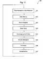
- FIG. 7is a flow diagram depicting an example of a method for alerting a processor 150 .
- the processors 12 of the embodiment describedwill “become inactive” while awaiting an input. Such an input can be from a neighboring processor 12 , as in the embodiment described in relation to FIGS. 1 through 4 .
- the processors 12 that have communication ports 38 that abut the edge of the die 14can have additional circuitry, either designed into such processor 12 or else external to the processor 12 but associated therewith, to cause such communication port 38 to act as an external I/O port 39 .
- the inventive combinationcan provide the additional advantage that the “inactive” processor 12 can be poised and ready to activate and spring into some prescribed action when an input is received. This process is referred to as a worker mode.
- Each processor 12is programmed to JUMP to an address when it is started. That address will be the address of the first instruction word 48 that will start that particular processor 12 on its designated job.
- the instruction wordcan be located, for example, in the ROM 26 .
- a processor 12may load a program, such as a program known as a worker mode loop.
- the worker mode loop for center processors 12 , edge processors 12 , and corner processors 12will be different.
- some processors 12may have specific tasks at boot-up in ROM associated with their positions within the array 10 . Worker mode loops will be described in greater detail hereinafter.
- a processor 12is caused to “become inactive” such that it is awaiting input from a neighbor processor 12 , or more than one (as many as all four) neighbor processors or, in the case of an “edge” processor 12 an external input, or some combination of external inputs and/or inputs from a neighbor processor 12 .
- a processor 12can “become inactive” awaiting completion of either a read or a write operation.
- the waiting processor 12will have set its read line 18 high awaiting a “write” from the neighbor or outside source. Indeed, it is presently anticipated that will be the usual condition. However, it is within the scope of the invention that the waiting processor 12 will have set its write line 20 high and, therefore, that it will become activated when the neighbor or outside source “reads” from it.
- the inactive processor 12is caused to resume operation because the neighboring processor 12 or external device 39 has completed the transaction being awaited. If the transaction being awaited was the receipt of an instruction word 48 to be executed, then the processor 12 will proceed to execute the instructions therein. If the transaction being awaited was the receipt of data, then the processor 12 will proceed to execute the next instruction in queue, which will be either the instruction in the next slot 54 in the present instruction word 48 , or else the next instruction word 48 will be loaded and the next instruction will be in slot 0 of that next instruction word 48 . In any case, while being used in the described manner, then that next instruction will begin a sequence of one or more instructions for handling the input just received.
- Options for handling such inputcan include reacting to perform some predefined function internally, communicating with one or more of the other processors 12 in the array 10 , or even ignoring the input (just as conventional prior art interrupts may be ignored under prescribed conditions).
- the optionsare depicted in the view of FIG. 7 as an “act on input” operation 156 . It should be noted that, in some instances, the content of the input may not be important. In some cases, for example, it may be only the very fact that an external device has attempted communication that is of interest.
- a processor 12When a processor 12 has one or more of its read lines 18 (or a write line 20 ) set high, it can be said to be in an “alert” condition. In the alert condition, the processor 12 is ready to immediately execute any instruction sent to it on the data bus 16 corresponding to the read line or lines 18 that are set high or, alternatively, to act on data that is transferred over the data bus 16 . Where there is an array of processors 12 available, one or more can be used, at any given time, to be in the above described alert condition such that any of a prescribed set of inputs will trigger it into action.
- a processorcan be placed in the alert condition and dedicated to awaiting the input of interest, such that not a single instruction period is wasted in beginning execution of the instructions triggered by such input.
- processors in the alert conditionwill actually be “inactive”, meaning that they are using essentially no power, but “alert” in that they will be instantly triggered into action by an input.
- alert conditioncould be embodied in a processor even if it were not “inactive”.
- the described alert conditioncan be used in essentially any situation where a conventional prior art interrupt (either a hardware interrupt or a software interrupt) might have otherwise been used.
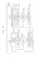
- FIG. 8is another example of a processor alert method 150 a .
- Thisis but one example wherein interaction between a monitoring processor 12 f ( FIG. 1 ) and another processor 12 g ( FIG. 1 ) that is assigned to some other task may be desirable or necessary.
- Thisis indicative of the nature of the cooperative coprocessor approach of the present invention, wherein each of the processors 12 has its own assignment which it carries out generally independently, except for those occasions when interaction is accomplished as described herein.
- This inventionprovides an alternative to the use of interrupts to handle inputs, whether such inputs come from an external input device, or from another processor 12 in the array 10 .
- processors 12can be assigned to receive and act upon certain inputs.
- the “activate” operation 154 , and the “act on input” operation 156each are accomplished as described previously herein in relation to the first example of the processor alert method 150 .
- the processor 12 fenters a “send info?” decision operation 158 wherein, according to its programming, it is determined if the input just received requires the attention of the other processor 12 g . If no, then the processor 12 f returns to inactive but alert status, or some other alternative such as was discussed previously herein.
- the processor 12 finitiates communication with the processor 12 g as described in detail previously herein in a “send to other” operation 160 .
- the processor 12 fcould be sending instructions such as it may have generated internally in response to the input from the external device 82 .
- the processor 12 fcould pass on data to the processor 12 g and such data could be internally generated in processor 12 or else “passed through” from the external device 82 .
- the processor 12 fin some situations, might attempt to read from the processor 12 g when it receives an input from the external device 82 . All of these opportunities are available to the programmer.
- the processor 12 gis generally executing code to accomplish its assigned primary task, whatever that might be, as indicated in an “execute primary function” operation 162 . However, if the programmer has decided that occasional interaction between the processors 12 f and 12 g is desirable, then the programmer will have provided that the processor 12 g occasionally pause to see if one or more of its neighbors has attempted a communication, as indicated in a “look for input” operation 166 . An “input?” decision operation 168 is made in the event that there is a communication waiting (as, for example, if the processor 12 f has already initiated a write to the processor 12 g ).
- the processor 12 gwill complete the communication, as described in detail previously herein, in a “receive from other” operation 170 . If no, then the processor 12 g will return to the execution of its assigned function, as shown in FIG. 8 . After the “receive from other” operation 170 , the processor 12 g will act on the input received in an “act on input” operation 172 . As mentioned above, the programmer could have provided that the processor 12 g would be expecting instructions such as input, in which case the processor 12 g would execute the instructions as described previously herein. Alternatively, the processor 12 g might be programmed to be expecting data to act upon.
- the processor 12 greturns to the accomplishment of its primary function (that is, it returns to the “execute primary function” operation 162 ).
- the programmingmight be such that certain inputs received from the processor 12 f will cause it to abort its previously assigned primary function and begin a new one, or else it might simply temporarily stop and await further input.
- the various possibilities for action hereare limited only by the imagination of the programmer.
- a given processor 12need not be interrupted while it is performing a task because another processor 12 is assigned the task of monitoring and handling inputs that might otherwise require an interrupt.
- the processor 12 that is busy handling another taskalso cannot be disturbed unless and until its programming provides that it look to its ports 38 for input. Therefore, it will sometimes be desirable to cause the processor 12 to pause or suspend its current task to look for other inputs.
- the concept of “Pause” and how it is usedwill be discussed in greater detail later.
- Each port 38 between processors 12comprises data lines 22 and one read line 18 and one write line 20 , which inclusively make up the data bus 16 .
- each port 38also comprises handshake control signals.
- the data lines 22connect between the ports 38 of two adjacent processors 12 .
- a word or op codemay reside in the T register 44 of processor 12 e during a STORE (write) instruction; the write line 20 of processor 12 e would then be set high.
- the read line 18 of processor 12 cis set high, then data is transferred into the T register 44 of processor 12 c in a FETCH (read) instruction. After the transaction is complete, both the read line 18 and the write line 20 are set low. In this example, this data becomes an instruction when it is read by the P register 40 c.
- a processor 12When a processor 12 reads a message, the message could be in the form of data, instructions, or signals. Instructions may be stored into memory and used later by the same processor 12 , or stored into and executed directly from a port 38 by a different processor 12 . If a processor 12 is reading from memory using its P register 40 c , it will either immediately execute the instruction by putting the instruction into the instruction register 30 a , or it will read the message as data and put it into the T register 44 . A FETCH instruction will read a message as data when the FETCH instruction is directed or addressed to a port 38 . If a JUMP or CALL instruction is to a port 38 , or a RETURN instruction is to a port 38 address, then the P register 40 c will read what is written to the port 38 as instructions and the instruction will be treated as executable code.
- a receiving processor 12could read a message as data and then write a message as data.
- a message that is routedi.e. sent from one processor 12 to a non-adjacent processor 12 through intermediary processors 12 ) is interpreted as data and read into the T register 44 of each successive processor 12 until the intended recipient is reached, then the message is interpreted as code (read from the P register 40 c ) and then executed.
- FIG. 1showed an array 10 of interconnected processors 12 located on a single die 14 ; a total of 24 processors 12 were given as an example, wherein each processor 12 has several pins located about its periphery.
- Each processor 12has four ports 38 that are designated as right, down, left, and up (RDLU).
- processor 12 ehas four adjacent processors 12 , wherein processor 12 b is the right neighbor, processor 12 d is the down neighbor, processor 12 c is the left neighbor, and processor 12 a is the up neighbor, all with respect to the center processor 12 e . Even though the edge processors 12 have only three adjacent neighbors and the corner processors 12 have only two adjacent neighbors, these edge and corner processors 12 still have four ports 38 which are also designated as RDLU.
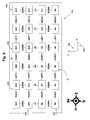
- FIG. 9is a block diagrammatic depiction of an alternative array 10 a .
- the array 10 ahas twenty four (24) processors 12 .
- the processors 12are arranged in a particular relative orientation referred to as “mirroring”. That is, the processors 12 in the second and fourth rows 173 from the top of the array 10 a have been flipped about their x-axes 174 , so that the down ports 38 d are now facing upward. All of the processors 12 in the second, fourth, and sixth columns 176 with respect to the left side of the array 10 a have been flipped about their y-axes 178 , such that the right ports 38 b are now facing towards the left side of the array 10 .
- processors N 6 , N 8 , N 10 , N 18 , N 20 and N 22maintaining their original RDLU orientations; processors N 0 , N 2 , N 4 , N 12 , N 14 , and N 16 having been flipped about their x-axes 174 only; processors N 7 , N 9 , N 11 , N 19 , N 21 , and N 23 having been flipped about their y-axes 178 only; and nodes N 1 , N 3 , N 5 , N 13 , N 15 , and N 17 having been flipped about both their x-axes 174 and their y-axes 178 .
- NSEWNorth, South, East and West
- the directions of North, South, East, and Westmaintain their relative directions, even with mirroring. This is relevant during routing, which was previously described as sending a message from a processor 12 to another non-adjacent processor 12 through intermediary processors 12 .
- Directions (NSEW)are in a table located in ROM 26 .
- Left ports 38 c and up ports 38 ado not connect to anything internal to the array 10 a when they are on the outside border of the array 10 a although, as discussed previously herein, they will probably connect to an external I/O port 39 ( FIG. 1 ).
- Down ports 38 d and right ports 38 balways connect to another processor 12 so long as the number of rows and columns is an even number.
- processor N 7has four orthogonally adjacent neighbors, namely N 6 which is connected to right port 38 b , N 1 which is connected to down port 38 d , N 8 which is connected to left port 38 c , and N 13 which is connected to the up port 38 a .
- 9 ais an expanded view of four nodes, namely N 7 , N 8 , N 13 , and N 14 from FIG. 9 , with right port 38 b , down port 38 d , left port 38 c , and up port 38 a notations.
- Each processor 12has an 18 bit I/O register 47 , as shown in FIG. 3 .
- Each I/O register 47contains, inter alia, information as to whether an adjacent neighbor is reading from or writing to its ports 38 .
- FIG. 10is a partial view of an I/O register 47 for a processor 12 .
- Bits B 9 through B 16indicate the read and write status for a processor 12 .
- the I/O register 47contains the read and write handshake status bits 50 on its communication ports 38 . These are read-only bits 50 . By reading these, a processor 12 can see if a neighbor is inactive waiting to write to one of its ports 38 or is inactive waiting to read from one of its ports 38 .
- the I/O register 47 write line status bit of processor 12will go high, indicating that a write message from that particular neighbor is waiting to be sent. Likewise, if a neighbor is waiting to read from processor 12 , then the I/O register 47 read line status bit of processor 12 will go high, indicating that a read message for that particular neighbor is waiting to be received.
- the I/O register 47 for Node 7indicates the read and write status bits (B 16 and B 15 , respectively) for the right port 38 b , which is connected to processor N 6 in this example.
- Bits B 14 and B 13are the read and write status bits, respectively, for the down port 38 d (connected to processor N 1 ); bits B 12 and B 11 are the read and write status bits, respectively, for the left port 38 c (connected to processor N 8 ); and bits B 10 and B 9 are the read and write status bits, respectively, for the up port 38 a (connected to processor N 13 ).
- bits 16 - 9always give the read and write status of adjacent nodes in the order of right, down, left, and up (RDLU).
- I/O register 47Another explanation of the I/O register 47 is as follows with continued reference to FIG. 10 , which shows a partial I/O register for Node 7 . If bit B 16 is high, then there is a read request from processor N 6 ; if bit B 15 is high, then there is a write request from processor N 6 ; if bit B 14 is high, then there is a read request from processor N 1 ; and so forth.
- PAUSEcauses a processor 12 to temporarily suspend its processing tasks or remain inactive in order to check for incoming data or instructions.
- a NOP(also referred to as a “no-op”) is a no operation instruction, and is designated by four dots ( . . . ) in the instruction code.
- a NOPmay be used in the instance when using some or all of the available slots 54 might be unnecessary or undesirable.
- four NOPs( . . . ) are used as a message header, in part because it must be safe to throw away the header (as after being activated) and also safe to execute the header (as when already executing or taking a break from executing the processor's own code), both of which conditions are met by a NOP instruction. It also has to be safe for multiple messages to arrive from different directions generally simultaneously. When each message begins with four NOPs, a simultaneous reading of two or more different messages will not be catastrophic since each processor is reading the same message header.
- a processor 12can be designated as primarily a worker or “production type” processor 12 . In the absence of any other instructions, this processor 12 can become a worker by default, and perform a worker mode loop 200 as in FIG. 11 , the loop being located in ROM. This worker processor 12 remains asleep or inactive until a message header containing four NOPS is sent to the worker processor 12 at the start of the worker mode loop 200 .
- FIG. 11is a flow diagram representing an example of a worker mode loop 200 which utilizes a PAUSE routine. When a worker processor 12 is inactive in a default worker mode loop 200 in ROM, the four NOPs of the message header are read as data in a “read message” operation 210 .
- a FETCH A instructionreads one word as data, which is four NOPs from a neighbor processor 12 , which is placed into the T register 44 of the worker processor 12 . Reading these four NOPS will wake up the worker processor 12 , as indicated by a “wake up” operation 211 in the flow chart of FIG. 11 .
- the “wake-up” messagewill activate the worker processor 12 .
- the contents or addresses of the B register 40 bare pointed at the I/O register 47 as a default setting, and therefore a FETCH B instruction will read the contents of the I/O register 47 in a “read I/O register” operation 212 to determine from which port the message was sent.
- a “begin pause” operation 213the worker processor 12 is absent of any processing activities, in order to prepare for the next step of “check the appropriate port(s)” operation 214 , according to the contents of the I/O register 47 that were read in the previous step 212 .
- the step of “execute message(s)” operation 215 from the appropriate port(s)occurs next.
- PAUSEwill end in an “end pause” operation 216 .
- the worker processor 12will become inactive in an “asleep/inactive” operation 217 , and wait until another message header arrives to activate or wake the worker processor 12 .
- all worker processors 12sleep and PAUSE.
- the worker processor 12sleeps, wakes up and reads the I/O register 47 where all neighbor processor 12 write requests are checked, begins PAUSE, and then executes the incoming message.
- At the end of an incoming messagethere is a return (;), or a JUMP to a port 38 with a return (;).
- the worker processor 12then goes back to the PAUSE routine, checks the next bit in the I/O register 47 for another message, executes the message, if any, then returns to the worker loop and goes to sleep waiting for more messages.
- PAUSEtreats incoming messages that are present as waking tasks, and treats ports 38 with nothing on them as sleeping tasks.
- FIG. 12The second occurrence of using PAUSE is shown in FIG. 12 , where a processor 12 is “processing a primary function” operation 220 . From time to time, the processor 12 will check the I/O register 47 in a “read I/O register” operation 221 to check the incoming status of adjacent processors 12 . If the I/O register 47 indicates that there is an incoming message, then the processor 12 will PAUSE in a “call pause” operation 222 . The processor 12 will then check the port 38 which was indicated by the I/O register 47 in a “check port for input” operation 223 .
- the processor 12will “execute all the code in the incoming message” operation 225 , including the four NOPs. After executing the incoming message, there is a “last port done?” decision operation 226 made as to whether there are other ports 38 waiting to send a message. If other port(s) need to be checked for possible input, then operations are repeated starting at step 223 with a “check port for input” operation. If there is no input there, as indicated by decision 224 , the processor 12 will go back to its original task (step 220 )—it will never go to sleep under those conditions. After checking all ports 38 in the order of right, down, left, and up (RDLU) for incoming messages and executing any code, the last port will be done (step 226 ), and the processor 12 will return to its original primary function at step 220 .
- RDLUdown, left, and up
- That processor 12wakes up with a data read.
- the processor 12can read with the A register 40 a (data) or the B register 40 b (data), or the P register 40 c (data or code); reading a whole message with the P register 40 c means it will execute an entire message including the four NOPs.
- a processor 12can read all four ports 38 as a worker, then go to sleep if no message is waiting ( FIG. 11 ). If a processor 12 is busy doing a task (loop), then a PAUSE call can be worked into a task ring to suspend the first task. The main task will be suspended and it will read the four ports 38 which adds four more tasks to the task ring, then it goes back to the main suspended task ( FIG. 12 ).
- Processors with I/O pins connectedhave bits in the I/O port 39 that set and show the status of those pins. Some pins are read-only and can be read by reading a bit in an I/O port 39 . Some pins are read/write and can be read or written by reading or writing bits in the I/O register 47 . After a read or write has been completed, the handshake signals are gone and are not readable in the I/O register 47 . Pins connected to the wake-up pin handshake circuit of an unconnected port will not be visible in the I/O register 47 .
- Serial processorshave their serial input pin connected to an I/O register bit (bit 17 ) where they can be read as data, but they are also connected to the handshake line of an unconnected corn port.
- a processor 12 that reads that unconnected corn portwill wake up when data on the pin tells the processor 12 that a write to the pin or phantom port is taking place.
- the processor 12When a real port 38 is read, the processor 12 will sleep until it gets the write handshake signal and will then wake up reading the data.
- the ROM codedistinguishes between a processor 12 being awakened by a pin and being awakened by a port 38 by reading the pin after the processor 12 is awake. If the pin is low, the processor 12 reads the I/O register 47 and pauses. If the pin is high, the processor 12 performs serial boot code.
- a read or write handshake bitis raised.
- the paired read or write handshake bitis raised by the other processor 12 , all bits raised by that processor 12 are lowered, the processors 12 wake up, and the data is transferred. After the data is transferred, any read/write handshake flag bits that were raised are lowered.
- a processor 12JUMPs to RDLU (the name of the address of four neighbor ports 38 ), it tries to read and raises read flags on all four ports 38 . It then goes to sleep in essentially a no power mode. When a neighbor(s) writes to one or more of these ports 38 and raises the write flag(s), all port 38 flags are reset and the first processor 12 wakes up. The same thing happens if the processor 12 reads the address using the A register 40 a or the B register 40 b and a data FETCH or STORE. It goes to sleep until one of the four (or three or two) neighbors wakes it up with data.
- a wake-up pinis read as part of an address four port 38 read and the pin is not high, then the processor 12 knows that the wake-up came from one of the other three neighbors.
- Serial boots in ROM on serial boot processors 12come from a pin which wakes up the processor 12 ; if the pin is high, then code is loaded from the serial pin and booted by the processor 12 .
- X0stands for execute on the 0 node of the RAM server; messages headed for node 0 on certain paths are defined in ROM. One must not route messages against each other. PAUSE allows messages to be routed safely.
- a RAM server buffer(on node 6, a node next to the RAM server) allows incoming messages to node 0 of the RAM server to be buffered in RAM on node 6 so that they do not back up and block messages sent out from the RAM server. This is the recommended routing path that doesn't conflict with X0.
- a set of tasksresides on a port 38 or ports 38 and local memory.
- FETCH B and PAUSEwill sequentially examine all ports 38 for incoming executable code and treat ports 38 as tasks. Instructions on a port 38 can be executed directly from the port 38 without loading into the processor's RAM first.
- PAUSE routine between multiple processors 12has been disclosed herein with reference to Forth, all of the concepts of the PAUSE routine between multiple processors 12 could be applied to other programming languages as well.
Landscapes
- Engineering & Computer Science (AREA)
- Theoretical Computer Science (AREA)
- Physics & Mathematics (AREA)
- General Engineering & Computer Science (AREA)
- General Physics & Mathematics (AREA)
- Multi Processors (AREA)
Abstract
Description
Claims (35)
Priority Applications (6)
| Application Number | Priority Date | Filing Date | Title |
|---|---|---|---|
| US11/653,187US7966481B2 (en) | 2006-02-16 | 2007-01-12 | Computer system and method for executing port communications without interrupting the receiving computer |
| EP07250647AEP1821211A3 (en) | 2006-02-16 | 2007-02-15 | Cooperative multitasking method in a multiprocessor system |
| TW96105683ATW200809529A (en) | 2006-02-16 | 2007-02-15 | Computer system with increased operating efficiency |
| KR1020077009922AKR20090016644A (en) | 2006-02-16 | 2007-02-16 | Computer system increases operational efficiency |
| JP2008555371AJP2009527815A (en) | 2006-02-16 | 2007-02-16 | Computer system with increased operating efficiency |
| PCT/US2007/004082WO2007098025A2 (en) | 2006-02-16 | 2007-02-16 | Computer system with increased operating efficiency |
Applications Claiming Priority (7)
| Application Number | Priority Date | Filing Date | Title |
|---|---|---|---|
| US11/355,513US7904695B2 (en) | 2006-02-16 | 2006-02-16 | Asynchronous power saving computer |
| US78826506P | 2006-03-31 | 2006-03-31 | |
| US79734506P | 2006-05-03 | 2006-05-03 | |
| US11/441,818US7934075B2 (en) | 2006-02-16 | 2006-05-26 | Method and apparatus for monitoring inputs to an asyncrhonous, homogenous, reconfigurable computer array |
| US81808406P | 2006-06-30 | 2006-06-30 | |
| US84949806P | 2006-09-29 | 2006-09-29 | |
| US11/653,187US7966481B2 (en) | 2006-02-16 | 2007-01-12 | Computer system and method for executing port communications without interrupting the receiving computer |
Related Parent Applications (2)
| Application Number | Title | Priority Date | Filing Date |
|---|---|---|---|
| US11/355,513Continuation-In-PartUS7904695B2 (en) | 2005-05-26 | 2006-02-16 | Asynchronous power saving computer |
| US11/441,818Continuation-In-PartUS7934075B2 (en) | 2006-02-16 | 2006-05-26 | Method and apparatus for monitoring inputs to an asyncrhonous, homogenous, reconfigurable computer array |
Publications (2)
| Publication Number | Publication Date |
|---|---|
| US20070226457A1 US20070226457A1 (en) | 2007-09-27 |
| US7966481B2true US7966481B2 (en) | 2011-06-21 |
Family
ID=38534964
Family Applications (1)
| Application Number | Title | Priority Date | Filing Date |
|---|---|---|---|
| US11/653,187Expired - Fee RelatedUS7966481B2 (en) | 2006-02-16 | 2007-01-12 | Computer system and method for executing port communications without interrupting the receiving computer |
Country Status (1)
| Country | Link |
|---|---|
| US (1) | US7966481B2 (en) |
Families Citing this family (6)
| Publication number | Priority date | Publication date | Assignee | Title |
|---|---|---|---|---|
| US7937557B2 (en)* | 2004-03-16 | 2011-05-03 | Vns Portfolio Llc | System and method for intercommunication between computers in an array |
| US7904695B2 (en) | 2006-02-16 | 2011-03-08 | Vns Portfolio Llc | Asynchronous power saving computer |
| US7904615B2 (en) | 2006-02-16 | 2011-03-08 | Vns Portfolio Llc | Asynchronous computer communication |
| US7966481B2 (en) | 2006-02-16 | 2011-06-21 | Vns Portfolio Llc | Computer system and method for executing port communications without interrupting the receiving computer |
| KR101738641B1 (en) | 2010-12-17 | 2017-05-23 | 삼성전자주식회사 | Apparatus and method for compilation of program on multi core system |
| US10599208B2 (en)* | 2015-09-08 | 2020-03-24 | Toshiba Memory Corporation | Memory system and controller |
Citations (211)
| Publication number | Priority date | Publication date | Assignee | Title |
|---|---|---|---|---|
| US3757306A (en) | 1971-08-31 | 1973-09-04 | Texas Instruments Inc | Computing systems cpu |
| US3868677A (en) | 1972-06-21 | 1975-02-25 | Gen Electric | Phase-locked voltage-to-digital converter |
| US4107773A (en) | 1974-05-13 | 1978-08-15 | Texas Instruments Incorporated | Advanced array transform processor with fixed/floating point formats |
| US4215401A (en) | 1978-09-28 | 1980-07-29 | Environmental Research Institute Of Michigan | Cellular digital array processor |
| US4215422A (en) | 1978-05-22 | 1980-07-29 | International Business Machines Corporation | Selectively modifiable phrase storage for a typewriter |
| US4298932A (en) | 1979-06-11 | 1981-11-03 | International Business Machines Corporation | Serial storage subsystem for a data processor |
| US4462074A (en) | 1981-11-19 | 1984-07-24 | Codex Corporation | Do loop circuit |
| GB2154343A (en) | 1984-02-16 | 1985-09-04 | Xerox Corp | Adaptive self repairing processor array |
| US4589067A (en) | 1983-05-27 | 1986-05-13 | Analogic Corporation | Full floating point vector processor with dynamically configurable multifunction pipelined ALU |
| US4593351A (en) | 1981-06-12 | 1986-06-03 | International Business Machines Corporation | High speed machine for the physical design of very large scale integrated circuits |
| US4665494A (en) | 1982-12-17 | 1987-05-12 | Victor Company Of Japan, Limited | Spectrum display device for audio signals |
| US4672331A (en) | 1983-06-21 | 1987-06-09 | Cushing Vincent J | Signal conditioner for electromagnetic flowmeter |
| EP0227319A2 (en) | 1985-12-26 | 1987-07-01 | Analog Devices, Inc. | Instruction cache memory |
| US4739474A (en)* | 1983-03-10 | 1988-04-19 | Martin Marietta Corporation | Geometric-arithmetic parallel processor |
| US4742511A (en)* | 1985-06-13 | 1988-05-03 | Texas Instruments Incorporated | Method and apparatus for routing packets in a multinode computer interconnect network |
| US4789927A (en) | 1986-04-07 | 1988-12-06 | Silicon Graphics, Inc. | Interleaved pipeline parallel processing architecture |
| US4821231A (en) | 1983-04-18 | 1989-04-11 | Motorola, Inc. | Method and apparatus for selectively evaluating an effective address for a coprocessor |
| US4868745A (en) | 1986-05-30 | 1989-09-19 | Hewlett-Packard Company | Data processing system and method for the direct and indirect execution of uniformly structured object types |
| US4942517A (en) | 1987-10-08 | 1990-07-17 | Eastman Kodak Company | Enhanced input/output architecture for toroidally-connected distributed-memory parallel computers |
| US4943909A (en) | 1987-07-08 | 1990-07-24 | At&T Bell Laboratories | Computational origami |
| US4961167A (en) | 1988-08-26 | 1990-10-02 | Mitsubishi Denki Kabushiki Kaisha | Substrate bias generator in a dynamic random access memory with auto/self refresh functions and a method of generating a substrate bias therein |
| US4984151A (en) | 1985-03-01 | 1991-01-08 | Advanced Micro Devices, Inc. | Flexible, next-address generation microprogram sequencer |
| US5021947A (en) | 1986-03-31 | 1991-06-04 | Hughes Aircraft Company | Data-flow multiprocessor architecture with three dimensional multistage interconnection network for efficient signal and data processing |
| CN1051995A (en) | 1989-11-21 | 1991-06-05 | 德国Itt工业股份有限公司 | Data-driven array processor |
| US5029124A (en) | 1988-05-17 | 1991-07-02 | Digital Equipment Corporation | Method and apparatus for providing high speed parallel transfer of bursts of data |
| US5053952A (en) | 1987-06-05 | 1991-10-01 | Wisc Technologies, Inc. | Stack-memory-based writable instruction set computer having a single data bus |
| US5159338A (en) | 1990-11-30 | 1992-10-27 | Kabushiki Kaisha Toshiba | Sampling frequency conversion apparatus |
| EP0156654B1 (en) | 1984-03-29 | 1993-02-24 | Mitsubishi Denki Kabushiki Kaisha | Control method for a half-duplex data transmission system |
| US5218682A (en) | 1991-05-10 | 1993-06-08 | Chrysler Corporation | Two-way handshake circuit and method for communication between processors |
| US5317735A (en) | 1990-06-14 | 1994-05-31 | U.S. Philips Corporation | System for parallel computation with three phase processing in processor tiers in which new instructions trigger execution and forwarding |
| US5319757A (en) | 1984-11-21 | 1994-06-07 | Harris Corporation | FORTH specific language microprocessor |
| US5359568A (en) | 1992-06-06 | 1994-10-25 | Motorola, Inc. | FIFO memory system |
| US5375238A (en) | 1990-11-20 | 1994-12-20 | Nec Corporation | Nesting management mechanism for use in loop control system |
| US5377333A (en) | 1991-09-20 | 1994-12-27 | Hitachi, Ltd. | Parallel processor system having computing clusters and auxiliary clusters connected with network of partial networks and exchangers |
| US5386585A (en) | 1993-02-03 | 1995-01-31 | Intel Corporation | Self-timed data pipeline apparatus using asynchronous stages having toggle flip-flops |
| US5390304A (en)* | 1990-09-28 | 1995-02-14 | Texas Instruments, Incorporated | Method and apparatus for processing block instructions in a data processor |
| US5396609A (en) | 1989-01-19 | 1995-03-07 | Gesellschaft Fur Strahlen- Und Umweltforschung Mbh (Gsf) | Method of protecting programs and data in a computer against unauthorized access and modification by monitoring address regions |
| DE3937807C2 (en) | 1988-11-19 | 1995-04-06 | Vaillant Joh Gmbh & Co | Method for transferring data between two sending and receiving stations |
| US5434989A (en) | 1991-02-19 | 1995-07-18 | Matsushita Electric Industrial Co., Ltd. | Cache memory for efficient access with address selectors |
| US5440749A (en) | 1989-08-03 | 1995-08-08 | Nanotronics Corporation | High performance, low cost microprocessor architecture |
| US5475856A (en) | 1991-11-27 | 1995-12-12 | International Business Machines Corporation | Dynamic multi-mode parallel processing array |
| US5485624A (en) | 1991-06-19 | 1996-01-16 | Hewlett-Packard Company | Co-processor monitoring address generated by host processor to obtain DMA parameters in the unused portion of instructions |
| US5535417A (en) | 1993-09-27 | 1996-07-09 | Hitachi America, Inc. | On-chip DMA controller with host computer interface employing boot sequencing and address generation schemes |
| US5535393A (en) | 1991-09-20 | 1996-07-09 | Reeve; Christopher L. | System for parallel processing that compiles a filed sequence of instructions within an iteration space |
| EP0724221A2 (en) | 1995-01-26 | 1996-07-31 | International Business Machines Corporation | Method and apparatus for executing dissimilar seq. of instructions in the processor of a single-instruction-multiple data (SIMD) computer |
| US5551045A (en) | 1988-12-21 | 1996-08-27 | Mitsubishi Denki Kabushiki Kaisha | Microprocessor with reset execution from an arbitrary address |
| US5550489A (en) | 1995-09-29 | 1996-08-27 | Quantum Corporation | Secondary clock source for low power, fast response clocking |
| JP2509678Y2 (en) | 1991-01-29 | 1996-09-04 | 宇部興産株式会社 | Billet loader for extrusion press |
| GB2299422A (en) | 1995-03-30 | 1996-10-02 | Sony Uk Ltd | Object code allocation in multiple processor systems |
| US5581767A (en) | 1993-06-16 | 1996-12-03 | Nippon Sheet Glass Co., Ltd. | Bus structure for multiprocessor system having separated processor section and control/memory section |
| US5630154A (en)* | 1994-10-11 | 1997-05-13 | Hughes Aircraft Company | Programmable systolic array system arranged in a found arrangement for passing data through programmable number of cells in a time interleaved manner |
| US5649198A (en) | 1993-02-19 | 1997-07-15 | Fujitsu Limited | Mapping calculation units by dividing a calculation model which can be calculated in parallel on an application program |
| US5657485A (en) | 1994-08-18 | 1997-08-12 | Mitsubishi Denki Kabushiki Kaisha | Program control operation to execute a loop processing not immediately following a loop instruction |
| US5673423A (en) | 1988-02-02 | 1997-09-30 | Tm Patents, L.P. | Method and apparatus for aligning the operation of a plurality of processors |
| US5692197A (en) | 1995-03-31 | 1997-11-25 | Sun Microsystems, Inc. | Method and apparatus for reducing power consumption in a computer network without sacrificing performance |
| US5706491A (en) | 1994-10-18 | 1998-01-06 | Cyrix Corporation | Branch processing unit with a return stack including repair using pointers from different pipe stages |
| US5717943A (en) | 1990-11-13 | 1998-02-10 | International Business Machines Corporation | Advanced parallel array processor (APAP) |
| US5727194A (en) | 1995-06-07 | 1998-03-10 | Hitachi America, Ltd. | Repeat-bit based, compact system and method for implementing zero-overhead loops |
| US5737628A (en) | 1993-12-10 | 1998-04-07 | Cray Research, Inc. | Multiprocessor computer system with interleaved processing element nodes |
| US5740463A (en) | 1994-07-22 | 1998-04-14 | Mitsubishi Denki Kabushiki Kaisha | Information processing system and method of computation performed with an information processing system |
| US5752259A (en) | 1996-03-26 | 1998-05-12 | Advanced Micro Devices, Inc. | Instruction cache configured to provide instructions to a microprocessor having a clock cycle time less than a cache access time of said instruction cache |
| US5765015A (en) | 1990-11-13 | 1998-06-09 | International Business Machines Corporation | Slide network for an array processor |
| US5784602A (en)* | 1996-10-08 | 1998-07-21 | Advanced Risc Machines Limited | Method and apparatus for digital signal processing for integrated circuit architecture |
| US5826101A (en) | 1990-09-28 | 1998-10-20 | Texas Instruments Incorporated | Data processing device having split-mode DMA channel |
| US5832291A (en) | 1995-12-15 | 1998-11-03 | Raytheon Company | Data processor with dynamic and selectable interconnections between processor array, external memory and I/O ports |
| US5867330A (en) | 1994-11-11 | 1999-02-02 | Canon Kabushiki Kaisha | Reproducing apparatus detecting pilot signals by binary data processing |
| US5893148A (en) | 1994-03-03 | 1999-04-06 | International Business Machines Corporation | System and method for allocating cache memory storage space |
| US5911082A (en) | 1997-02-25 | 1999-06-08 | Audio Digitalimaging Inc. | Parallel processing building block chip |
| US5937202A (en)* | 1993-02-11 | 1999-08-10 | 3-D Computing, Inc. | High-speed, parallel, processor architecture for front-end electronics, based on a single type of ASIC, and method use thereof |
| US6003128A (en) | 1997-05-01 | 1999-12-14 | Advanced Micro Devices, Inc. | Number of pipeline stages and loop length related counter differential based end-loop prediction |
| US6023753A (en) | 1997-06-30 | 2000-02-08 | Billion Of Operations Per Second, Inc. | Manifold array processor |
| US6038655A (en) | 1993-02-09 | 2000-03-14 | Dallas Semiconductor Corporation | Microcontroller having register direct and register indirect addressing |
| EP0992896A1 (en) | 1998-10-06 | 2000-04-12 | Texas Instruments Inc. | Pipeline protection |
| US6057791A (en) | 1998-02-18 | 2000-05-02 | Oasis Design, Inc. | Apparatus and method for clocking digital and analog circuits on a common substrate to enhance digital operation and reduce analog sampling error |
| US6081215A (en) | 1998-07-06 | 2000-06-27 | Motorola, Inc. | High speed interlaced analog interface |
| US6085304A (en) | 1997-11-28 | 2000-07-04 | Teranex, Inc. | Interface for processing element array |
| US6092183A (en) | 1994-03-16 | 2000-07-18 | Hitachi, Ltd. | Data processor for processing a complex instruction by dividing it into executing units |
| US6094030A (en) | 1999-05-13 | 2000-07-25 | Deltatee Enterprises Ltd. | Resistance and charging monitor within a standby battery bank |
| US6101598A (en) | 1997-11-14 | 2000-08-08 | Cirrus Logic, Inc. | Methods for debugging a multiprocessor system |
| US6112296A (en) | 1997-12-18 | 2000-08-29 | Advanced Micro Devices, Inc. | Floating point stack manipulation using a register map and speculative top of stack values |
| US6145072A (en) | 1993-08-12 | 2000-11-07 | Hughes Electronics Corporation | Independently non-homogeneously dynamically reconfigurable two dimensional interprocessor communication topology for SIMD multi-processors and apparatus for implementing same |
| US6148392A (en) | 1998-09-08 | 2000-11-14 | Hyundai Electronics Industries Co., Ltd. | Low power implementation of an asynchronous stock having a constant response time |
| US6154809A (en) | 1995-11-10 | 2000-11-28 | Nippon Telegraph & Telephone Corporation | Mathematical morphology processing method |
| US6173389B1 (en) | 1997-12-04 | 2001-01-09 | Billions Of Operations Per Second, Inc. | Methods and apparatus for dynamic very long instruction word sub-instruction selection for execution time parallelism in an indirect very long instruction word processor |
| US6178525B1 (en) | 1997-02-27 | 2001-01-23 | Sgs-Thomson Microelectronics Limited | Trigger sequencing controller |
| US6192388B1 (en) | 1996-06-20 | 2001-02-20 | Avid Technology, Inc. | Detecting available computers to participate in computationally complex distributed processing problem |
| US6219685B1 (en) | 1998-09-04 | 2001-04-17 | Intel Corporation | Method to detect IEEE overflow and underflow conditions |
| US6223282B1 (en) | 1997-12-29 | 2001-04-24 | Samsung Electronics Co., Ltd. | Circuit for controlling execution of loop in digital signal processing chip |
| US6232905B1 (en) | 1999-03-08 | 2001-05-15 | Agere Systems Guardian Corp. | Clocking technique for reducing sampling noise in an analog-to-digital converter |
| US6233670B1 (en) | 1991-06-17 | 2001-05-15 | Mitsubishi Denki Kabushiki Kaisha | Superscalar processor with direct result bypass between execution units having comparators in execution units for comparing operand and result addresses and activating result bypassing |
| US6236645B1 (en) | 1998-03-09 | 2001-05-22 | Broadcom Corporation | Apparatus for, and method of, reducing noise in a communications system |
| US6279101B1 (en) | 1992-08-12 | 2001-08-21 | Advanced Micro Devices, Inc. | Instruction decoder/dispatch |
| US6307425B1 (en) | 1996-07-18 | 2001-10-23 | Micron Technology, Inc. | Clocking scheme and charge transfer switch for increasing the efficiency of a charge pump or other circuit |
| US6308229B1 (en) | 1998-08-28 | 2001-10-23 | Theseus Logic, Inc. | System for facilitating interfacing between multiple non-synchronous systems utilizing an asynchronous FIFO that uses asynchronous logic |
| US20020004912A1 (en) | 1990-06-01 | 2002-01-10 | Amphus, Inc. | System, architecture, and method for logical server and other network devices in a dynamically configurable multi-server network environment |
| US20020010844A1 (en) | 1998-06-10 | 2002-01-24 | Karen L. Noel | Method and apparatus for dynamically sharing memory in a multiprocessor system |
| US20020019951A1 (en) | 2000-08-02 | 2002-02-14 | Masahito Kubo | Timer adjusting system |
| EP1182544A2 (en) | 1989-06-22 | 2002-02-27 | Sun Microsystems, Inc. | Multiprocessor system with multiple instruction sources |
| US6353880B1 (en) | 1998-07-22 | 2002-03-05 | Scenix Semiconductor, Inc. | Four stage pipeline processing for a microcontroller |
| US6367005B1 (en) | 1998-04-21 | 2002-04-02 | Idea Corporation Of Delaware | System and method for synchronizing a register stack engine (RSE) and backing memory image with a processor's execution of instructions during a state saving context switch |
| US6381705B1 (en) | 1999-02-09 | 2002-04-30 | Stmicroelectronics S.A. | Method and device for reducing current consumption of a microcontroller |
| US6388600B1 (en) | 2000-11-13 | 2002-05-14 | Trw Inc. | Asynchronous superconductor serial multiply-accumulator |
| US6404663B2 (en) | 1999-06-14 | 2002-06-11 | Fujitsu Limited | Semiconductor integrated circuit having testing mode for modifying operation timing |
| US6404274B1 (en) | 1998-04-09 | 2002-06-11 | Kabushiki Kaisha Toshiba | Internal voltage generating circuit capable of generating variable multi-level voltages |
| US6427204B1 (en) | 1999-06-25 | 2002-07-30 | International Business Machines Corporation | Method for just in-time delivery of instructions in a data processing system |
| US6449709B1 (en) | 1998-06-02 | 2002-09-10 | Adaptec, Inc. | Fast stack save and restore system and method |
| US6460128B1 (en) | 1994-05-11 | 2002-10-01 | Intel Corporation | Mesh network with method and apparatus for interleaved binary exchange |
| WO2002088936A1 (en) | 2001-05-02 | 2002-11-07 | Portalplayer, Inc. | Multiprocessor communication system and method |
| US20020186159A1 (en) | 2001-05-03 | 2002-12-12 | Mario Reinhold | Amplitude detection for controlling the decision instant for sampling as a data flow |
| US6502141B1 (en) | 1999-12-14 | 2002-12-31 | International Business Machines Corporation | Method and system for approximate, monotonic time synchronization for a multiple node NUMA system |
| US20030005168A1 (en) | 2001-06-29 | 2003-01-02 | Leerssen Scott Alan | System and method for auditing system call events with system call wrappers |
| US20030009502A1 (en) | 2001-06-29 | 2003-01-09 | Nec Corporation | Complex vector operation processor with pipeline processing function and system using the same |
| US6507947B1 (en) | 1999-08-20 | 2003-01-14 | Hewlett-Packard Company | Programmatic synthesis of processor element arrays |
| US6507649B1 (en) | 1998-12-18 | 2003-01-14 | Ericsson Inc. | Mechanism and method for distributing ISUP stacks over multiple loosely coupled processors |
| US20030028750A1 (en) | 2001-07-25 | 2003-02-06 | Hogenauer Eugene B. | Method and system for digital signal processing in an adaptive computing engine |
| US6522282B1 (en) | 2001-11-07 | 2003-02-18 | Telefonaktiebolaget Lm Ericsson (Publ) | Estimation of timing offsets in parallel A/D converters |
| US20030035549A1 (en) | 1999-11-29 | 2003-02-20 | Bizjak Karl M. | Signal processing system and method |
| WO2003019356A1 (en) | 2001-08-22 | 2003-03-06 | Adelante Technologies B.V. | Pipelined processor and instruction loop execution method |
| US6542105B2 (en) | 2000-12-18 | 2003-04-01 | Canon Kabushiki Kaisha | A/D converter |
| US20030065905A1 (en) | 2001-10-01 | 2003-04-03 | Nec Corporation | Parallel computation processor, parallel computation control method and program thereof |
| US6560716B1 (en) | 1999-11-10 | 2003-05-06 | Lsi Logic Corporation | System for measuring delay of digital signal using clock generator and delay unit wherein a set of digital elements of clock generator identical to a set of digital elements of delay unit |
| US20030113031A1 (en) | 1997-04-15 | 2003-06-19 | Wal Gooitzen Siemen Van Der | Parallel pipeline image processing system |
| US20030135710A1 (en) | 2002-01-17 | 2003-07-17 | Farwell William D. | Reconfigurable processor architectures |
| US20030179123A1 (en) | 2002-03-22 | 2003-09-25 | Devilbiss Alan D. | Analog-to-digital conversion using a counter |
| US6636122B2 (en) | 2001-10-09 | 2003-10-21 | Zilog, Inc. | Analog frequency locked loop with digital oversampling feedback control and filter |
| US6647027B1 (en) | 1999-11-10 | 2003-11-11 | Lsi Logic Corporation | Method and apparatus for multi-channel data delay equalization |
| US20030217242A1 (en) | 2002-05-17 | 2003-11-20 | Samsung Electronics Co., Ltd. | System and method for synchronizing a plurality of processors in a processor array |
| US6657462B2 (en) | 2001-09-24 | 2003-12-02 | Broadcom Corporation | Conditional clock buffer circuit |
| US6665793B1 (en) | 1999-12-28 | 2003-12-16 | Institute For The Development Of Emerging Architectures, L.L.C. | Method and apparatus for managing access to out-of-frame Registers |
| US6671112B2 (en) | 1995-08-11 | 2003-12-30 | Fujitsu Limited | Semiconductor integrated circuit device |
| US20040003219A1 (en) | 2002-06-26 | 2004-01-01 | Teruaki Uehara | Loop control circuit and loop control method |
| US20040030859A1 (en) | 2002-06-26 | 2004-02-12 | Doerr Michael B. | Processing system with interspersed processors and communication elements |
| US20040059895A1 (en) | 2001-01-18 | 2004-03-25 | Christian May | Microprocessor circuit for portable data carriers and method for operating the circuit |
| US6725361B1 (en) | 2000-06-16 | 2004-04-20 | Transmeta Corporation | Method and apparatus for emulating a floating point stack in a translation process |
| US6732253B1 (en) | 2000-11-13 | 2004-05-04 | Chipwrights Design, Inc. | Loop handling for single instruction multiple datapath processor architectures |
| US20040098707A1 (en) | 2002-11-18 | 2004-05-20 | Microsoft Corporation | Generic wrapper scheme |
| US20040095264A1 (en) | 2002-11-14 | 2004-05-20 | Thomas John Carl | Power converter circuitry and method |
| US20040107332A1 (en) | 2002-10-30 | 2004-06-03 | Nec Electronics Corporation | Array-type processor |
| US20040143638A1 (en) | 2002-06-28 | 2004-07-22 | Beckmann Curt E. | Apparatus and method for storage processing through scalable port processors |
| US20040215929A1 (en)* | 2003-04-28 | 2004-10-28 | International Business Machines Corporation | Cross-chip communication mechanism in distributed node topology |
| US6826674B1 (en) | 1999-08-30 | 2004-11-30 | Ip Flex, Inc. | Program product and data processor |
| US6825843B2 (en) | 2002-07-18 | 2004-11-30 | Nvidia Corporation | Method and apparatus for loop and branch instructions in a programmable graphics pipeline |
| US20040250046A1 (en) | 2003-03-31 | 2004-12-09 | Gonzalez Ricardo E. | Systems and methods for software extensible multi-processing |
| US6845412B1 (en) | 2001-11-07 | 2005-01-18 | Lsi Logic Corporation | Method and system for a host processor to broadcast data to instruction or data memories of several processors in a multi-processor integrated circuit |
| US20050015572A1 (en) | 2003-07-09 | 2005-01-20 | Hiroshi Tanaka | Semiconductor integrated circuit |
| US20050027548A1 (en) | 2003-07-31 | 2005-02-03 | Jacobs Philip C. | Cost minimization of services provided by multiple service providers |
| US20050034029A1 (en) | 1999-01-29 | 2005-02-10 | Intermec Ip Corp. | Remote anomaly diagnosis and reconfiguration of an automatic data collection device platform over a telecommunications network |
| US6898721B2 (en) | 2001-06-22 | 2005-05-24 | Gallitzin Allegheny Llc | Clock generation systems and methods |
| US20050114565A1 (en) | 2003-03-31 | 2005-05-26 | Stretch, Inc. | Systems and methods for selecting input/output configuration in an integrated circuit |
| US20050149693A1 (en)* | 2000-02-24 | 2005-07-07 | Pts Corporation | Methods and apparatus for dual-use coprocessing/debug interface |
| US20050182581A1 (en) | 2002-05-14 | 2005-08-18 | Analysis And Measurement Services Corporation | Testing of wire systems and end devices installed in industrial processes |
| US6937538B2 (en) | 2000-02-02 | 2005-08-30 | Broadcom Corporation | Asynchronously resettable decoder for a semiconductor memory |
| US20050196060A1 (en) | 2004-03-03 | 2005-09-08 | Demin Wang | Curved wavelet transform for image and video compression |
| US20050206648A1 (en) | 2004-03-16 | 2005-09-22 | Perry Ronald N | Pipeline and cache for processing data progressively |
| US20050223204A1 (en) | 2004-03-30 | 2005-10-06 | Nec Electronics Corporation | Data processing apparatus adopting pipeline processing system and data processing method used in the same |
| US20050228904A1 (en) | 2004-03-16 | 2005-10-13 | Moore Charles H | Computer processor array |
| US6959372B1 (en) | 2002-02-19 | 2005-10-25 | Cogent Chipware Inc. | Processor cluster architecture and associated parallel processing methods |
| US20050237083A1 (en) | 2003-07-31 | 2005-10-27 | Actel Corporation, A California Corporation | Programmable system on a chip |
| US6966002B1 (en) | 1999-04-30 | 2005-11-15 | Trymedia Systems, Inc. | Methods and apparatus for secure distribution of software |
| US20050257037A1 (en) | 2003-04-04 | 2005-11-17 | Arm Limited | Controlling execution of a block of program instructions within a computer processing system |
| US20050262278A1 (en) | 2004-05-20 | 2005-11-24 | Schmidt Dominik J | Integrated circuit with a plurality of host processor family types |
| US6970895B2 (en) | 2001-10-01 | 2005-11-29 | Koninklijke Philips Electronics N.V. | Programmable delay indexed data path register file for array processing |
| US20060059377A1 (en) | 2001-04-18 | 2006-03-16 | Sherburne Robert W Jr | Low power clocking systems and methods |
| US7028163B2 (en) | 1998-06-22 | 2006-04-11 | Samsung Electronics, Co., Ltd. | Apparatus for controlling multi-word stack operations using a multi-bank stack in digital data processors |
| US20060082445A1 (en) | 1996-05-13 | 2006-04-20 | O'toole James E | Radio frequency data communications device |
| US20060101238A1 (en) | 2004-09-17 | 2006-05-11 | Pradip Bose | Adaptive fetch gating in multithreaded processors, fetch control and method of controlling fetches |
| US20060097901A1 (en) | 2004-10-08 | 2006-05-11 | Dieter Draxelmayr | Analog-to-digital converter operable with staggered timing |
| US20060149925A1 (en) | 1991-07-08 | 2006-07-06 | Seiko Epson Corporation | High-performance superscalar-based computer system with out-of-order instruction execution and concurrent results distribution |
| US7079046B2 (en) | 2003-03-28 | 2006-07-18 | Yokogawa Electric Corporation | Multi-point data acquisition apparatus |
| US7084793B2 (en) | 2003-01-15 | 2006-08-01 | Infineon Technologies Ag | Method and device for estimating time errors in time interleaved A/D converter system |
| US7089438B2 (en) | 2002-06-25 | 2006-08-08 | Micron Technology, Inc. | Circuit, system and method for selectively turning off internal clock drivers |
| US20060212867A1 (en) | 2005-03-17 | 2006-09-21 | Microsoft Corporation | Determining an actual amount of time a processor consumes in executing a portion of code |
| US20060218375A1 (en) | 2003-02-12 | 2006-09-28 | Swarztrauber Paul N | System and method of transferring data between a massive number of processors |
| US20060224831A1 (en) | 2005-04-04 | 2006-10-05 | Toshiba America Electronic Components | Systems and methods for loading data into the cache of one processor to improve performance of another processor in a multiprocessor system |
| US7131113B2 (en) | 2002-12-12 | 2006-10-31 | International Business Machines Corporation | System and method on generating multi-dimensional trace files and visualizing them using multiple Gantt charts |
| US20060248317A1 (en) | 2002-08-07 | 2006-11-02 | Martin Vorbach | Method and device for processing data |
| US20060248360A1 (en) | 2001-05-18 | 2006-11-02 | Fung Henry T | Multi-server and multi-CPU power management system and method |
| US20060259743A1 (en) | 2005-05-10 | 2006-11-16 | Masakazu Suzuoki | Methods and apparatus for power management in a computing system |
| US20060271764A1 (en) | 2005-05-24 | 2006-11-30 | Coresonic Ab | Programmable digital signal processor including a clustered SIMD microarchitecture configured to execute complex vector instructions |
| US20060279970A1 (en) | 2002-11-14 | 2006-12-14 | Kent Kernahan | Switching power converter controller |
| US20060279969A1 (en) | 2004-07-27 | 2006-12-14 | Silicon Laboratories Inc. | Distributed power supply system with separate SYNC control for controlling remote digital DC/DC converters |
| US20060279445A1 (en) | 2005-06-13 | 2006-12-14 | Kinyua Martin K | System and method for improved time-interleaved analog-to-digital converter arrays |
| US7155602B2 (en) | 2001-04-30 | 2006-12-26 | Src Computers, Inc. | Interface for integrating reconfigurable processors into a general purpose computing system |
| US7157934B2 (en) | 2003-08-19 | 2007-01-02 | Cornell Research Foundation, Inc. | Programmable asynchronous pipeline arrays |
| US7162573B2 (en) | 2003-06-25 | 2007-01-09 | Intel Corporation | Communication registers for processing elements |
| US20070035611A1 (en) | 2005-07-27 | 2007-02-15 | Chao-Hung Wu | Mobile audio/video data transmission system and method for the same |
| US20070036150A1 (en) | 1998-04-03 | 2007-02-15 | Pounds Gregory E | Systems and methods for TDM/packet communications using telephony station cards including voltage generators |
| US20070041438A1 (en) | 2004-01-30 | 2007-02-22 | Sony Corporation | Sampling rate conversion device and method, and audio device |
| US20070070079A1 (en) | 2002-01-17 | 2007-03-29 | University Of Washington | Programmable 3d graphics pipeline for multimedia applications |
| US20070113058A1 (en) | 2005-11-14 | 2007-05-17 | Texas Instruments Incorporated | Microprocessor with indepedent SIMD loop buffer |
| US20070153953A1 (en) | 2006-01-04 | 2007-07-05 | Matthias Garzarolli | Phase-Locked Loop |
| US7249357B2 (en) | 2001-08-20 | 2007-07-24 | Silicon Graphics, Inc. | Transparent distribution and execution of data in a multiprocessor environment |
| US7255476B2 (en) | 2004-04-14 | 2007-08-14 | International Business Machines Corporation | On chip temperature measuring and monitoring circuit and method |
| US20070192646A1 (en) | 2006-02-16 | 2007-08-16 | Moore Charles H | Asynchronous power saving computer |
| US20070192575A1 (en) | 2006-02-16 | 2007-08-16 | Moore Charles H | Microloop computer instructions |
| US20070192570A1 (en) | 2006-02-16 | 2007-08-16 | Moore Charles H | Execution of instructions directly from input source |
| US20070192566A1 (en) | 2006-02-16 | 2007-08-16 | Moore Charles H | Method and apparatus for monitoring inputs to a computer |
| US20070192504A1 (en) | 2006-02-16 | 2007-08-16 | Moore Charles H | Asynchronous computer communication |
| US7263624B2 (en) | 2000-05-12 | 2007-08-28 | Altera Corporation | Methods and apparatus for power control in a scalable array of processor elements |
| US7265640B1 (en) | 2004-12-23 | 2007-09-04 | Xilinx, Inc. | Circuit approach for common mode control in high-frequency clocks |
| US7269805B1 (en) | 2004-04-30 | 2007-09-11 | Xilinx, Inc. | Testing of an integrated circuit having an embedded processor |
| US20070226457A1 (en) | 2006-02-16 | 2007-09-27 | Moore Charles H | Computer system with increased operating efficiency |
| US7319355B2 (en) | 2006-01-03 | 2008-01-15 | Taiwan Semiconductor Manufacturing Co., Ltd. | Pulse generator |
| US7380100B2 (en) | 2001-09-07 | 2008-05-27 | Ipflex Inc. | Data processing system and control method utilizing a plurality of date transfer means |
| US7386689B2 (en) | 2000-08-31 | 2008-06-10 | Micron Technology, Inc. | Method and apparatus for connecting a massively parallel processor array to a memory array in a bit serial manner |
| US7403055B2 (en) | 2005-08-31 | 2008-07-22 | Infineon Technologies Ag | Duty cycle detector with first and second oscillating signals |
| US20080270648A1 (en) | 2007-04-27 | 2008-10-30 | Technology Properties Limited | System and method for multi-port read and write operations |
| US20080270751A1 (en) | 2007-04-27 | 2008-10-30 | Technology Properties Limited | System and method for processing data in a pipeline of computers |
| US7471643B2 (en) | 2002-07-01 | 2008-12-30 | Panasonic Corporation | Loosely-biased heterogeneous reconfigurable arrays |
| US7512728B2 (en) | 1998-08-31 | 2009-03-31 | Axis Systems, Inc | Inter-chip communication system |
| US7528756B2 (en) | 2007-03-22 | 2009-05-05 | Vns Portfolio Llc | Analog-to-digital converter system with increased sampling frequency |
- 2007
- 2007-01-12USUS11/653,187patent/US7966481B2/ennot_activeExpired - Fee Related
Patent Citations (218)
| Publication number | Priority date | Publication date | Assignee | Title |
|---|---|---|---|---|
| US3757306A (en) | 1971-08-31 | 1973-09-04 | Texas Instruments Inc | Computing systems cpu |
| US3868677A (en) | 1972-06-21 | 1975-02-25 | Gen Electric | Phase-locked voltage-to-digital converter |
| US4107773A (en) | 1974-05-13 | 1978-08-15 | Texas Instruments Incorporated | Advanced array transform processor with fixed/floating point formats |
| US4215422A (en) | 1978-05-22 | 1980-07-29 | International Business Machines Corporation | Selectively modifiable phrase storage for a typewriter |
| US4215401A (en) | 1978-09-28 | 1980-07-29 | Environmental Research Institute Of Michigan | Cellular digital array processor |
| US4298932A (en) | 1979-06-11 | 1981-11-03 | International Business Machines Corporation | Serial storage subsystem for a data processor |
| US4593351A (en) | 1981-06-12 | 1986-06-03 | International Business Machines Corporation | High speed machine for the physical design of very large scale integrated circuits |
| US4462074A (en) | 1981-11-19 | 1984-07-24 | Codex Corporation | Do loop circuit |
| US4665494A (en) | 1982-12-17 | 1987-05-12 | Victor Company Of Japan, Limited | Spectrum display device for audio signals |
| US4739474A (en)* | 1983-03-10 | 1988-04-19 | Martin Marietta Corporation | Geometric-arithmetic parallel processor |
| US4821231A (en) | 1983-04-18 | 1989-04-11 | Motorola, Inc. | Method and apparatus for selectively evaluating an effective address for a coprocessor |
| US4589067A (en) | 1983-05-27 | 1986-05-13 | Analogic Corporation | Full floating point vector processor with dynamically configurable multifunction pipelined ALU |
| US4672331A (en) | 1983-06-21 | 1987-06-09 | Cushing Vincent J | Signal conditioner for electromagnetic flowmeter |
| US4591980A (en) | 1984-02-16 | 1986-05-27 | Xerox Corporation | Adaptive self-repairing processor array |
| GB2154343A (en) | 1984-02-16 | 1985-09-04 | Xerox Corp | Adaptive self repairing processor array |
| EP0156654B1 (en) | 1984-03-29 | 1993-02-24 | Mitsubishi Denki Kabushiki Kaisha | Control method for a half-duplex data transmission system |
| US5319757A (en) | 1984-11-21 | 1994-06-07 | Harris Corporation | FORTH specific language microprocessor |
| US4984151A (en) | 1985-03-01 | 1991-01-08 | Advanced Micro Devices, Inc. | Flexible, next-address generation microprogram sequencer |
| US4742511A (en)* | 1985-06-13 | 1988-05-03 | Texas Instruments Incorporated | Method and apparatus for routing packets in a multinode computer interconnect network |
| EP0227319A2 (en) | 1985-12-26 | 1987-07-01 | Analog Devices, Inc. | Instruction cache memory |
| US5021947A (en) | 1986-03-31 | 1991-06-04 | Hughes Aircraft Company | Data-flow multiprocessor architecture with three dimensional multistage interconnection network for efficient signal and data processing |
| US4789927A (en) | 1986-04-07 | 1988-12-06 | Silicon Graphics, Inc. | Interleaved pipeline parallel processing architecture |
| US4868745A (en) | 1986-05-30 | 1989-09-19 | Hewlett-Packard Company | Data processing system and method for the direct and indirect execution of uniformly structured object types |
| US5053952A (en) | 1987-06-05 | 1991-10-01 | Wisc Technologies, Inc. | Stack-memory-based writable instruction set computer having a single data bus |
| US4943909A (en) | 1987-07-08 | 1990-07-24 | At&T Bell Laboratories | Computational origami |
| US4942517A (en) | 1987-10-08 | 1990-07-17 | Eastman Kodak Company | Enhanced input/output architecture for toroidally-connected distributed-memory parallel computers |
| US5673423A (en) | 1988-02-02 | 1997-09-30 | Tm Patents, L.P. | Method and apparatus for aligning the operation of a plurality of processors |
| US5029124A (en) | 1988-05-17 | 1991-07-02 | Digital Equipment Corporation | Method and apparatus for providing high speed parallel transfer of bursts of data |
| US4961167A (en) | 1988-08-26 | 1990-10-02 | Mitsubishi Denki Kabushiki Kaisha | Substrate bias generator in a dynamic random access memory with auto/self refresh functions and a method of generating a substrate bias therein |
| DE3937807C2 (en) | 1988-11-19 | 1995-04-06 | Vaillant Joh Gmbh & Co | Method for transferring data between two sending and receiving stations |
| US5551045A (en) | 1988-12-21 | 1996-08-27 | Mitsubishi Denki Kabushiki Kaisha | Microprocessor with reset execution from an arbitrary address |
| US5396609A (en) | 1989-01-19 | 1995-03-07 | Gesellschaft Fur Strahlen- Und Umweltforschung Mbh (Gsf) | Method of protecting programs and data in a computer against unauthorized access and modification by monitoring address regions |
| EP1182544A2 (en) | 1989-06-22 | 2002-02-27 | Sun Microsystems, Inc. | Multiprocessor system with multiple instruction sources |
| US5440749A (en) | 1989-08-03 | 1995-08-08 | Nanotronics Corporation | High performance, low cost microprocessor architecture |
| US6598148B1 (en) | 1989-08-03 | 2003-07-22 | Patriot Scientific Corporation | High performance microprocessor having variable speed system clock |
| US5410723A (en) | 1989-11-21 | 1995-04-25 | Deutsche Itt Industries Gmbh | Wavefront array processor for blocking the issuance of first handshake signal (req) by the presence of second handshake signal (ack) which indicates the readyness of the receiving cell |
| CN1051995A (en) | 1989-11-21 | 1991-06-05 | 德国Itt工业股份有限公司 | Data-driven array processor |
| US20020004912A1 (en) | 1990-06-01 | 2002-01-10 | Amphus, Inc. | System, architecture, and method for logical server and other network devices in a dynamically configurable multi-server network environment |
| US5317735A (en) | 1990-06-14 | 1994-05-31 | U.S. Philips Corporation | System for parallel computation with three phase processing in processor tiers in which new instructions trigger execution and forwarding |
| US5390304A (en)* | 1990-09-28 | 1995-02-14 | Texas Instruments, Incorporated | Method and apparatus for processing block instructions in a data processor |
| US5826101A (en) | 1990-09-28 | 1998-10-20 | Texas Instruments Incorporated | Data processing device having split-mode DMA channel |
| US5717943A (en) | 1990-11-13 | 1998-02-10 | International Business Machines Corporation | Advanced parallel array processor (APAP) |
| US5765015A (en) | 1990-11-13 | 1998-06-09 | International Business Machines Corporation | Slide network for an array processor |
| US5375238A (en) | 1990-11-20 | 1994-12-20 | Nec Corporation | Nesting management mechanism for use in loop control system |
| US5159338A (en) | 1990-11-30 | 1992-10-27 | Kabushiki Kaisha Toshiba | Sampling frequency conversion apparatus |
| JP2509678Y2 (en) | 1991-01-29 | 1996-09-04 | 宇部興産株式会社 | Billet loader for extrusion press |
| US5434989A (en) | 1991-02-19 | 1995-07-18 | Matsushita Electric Industrial Co., Ltd. | Cache memory for efficient access with address selectors |
| US5218682A (en) | 1991-05-10 | 1993-06-08 | Chrysler Corporation | Two-way handshake circuit and method for communication between processors |
| US6233670B1 (en) | 1991-06-17 | 2001-05-15 | Mitsubishi Denki Kabushiki Kaisha | Superscalar processor with direct result bypass between execution units having comparators in execution units for comparing operand and result addresses and activating result bypassing |
| US5485624A (en) | 1991-06-19 | 1996-01-16 | Hewlett-Packard Company | Co-processor monitoring address generated by host processor to obtain DMA parameters in the unused portion of instructions |
| US20060149925A1 (en) | 1991-07-08 | 2006-07-06 | Seiko Epson Corporation | High-performance superscalar-based computer system with out-of-order instruction execution and concurrent results distribution |
| US5535393A (en) | 1991-09-20 | 1996-07-09 | Reeve; Christopher L. | System for parallel processing that compiles a filed sequence of instructions within an iteration space |
| US5377333A (en) | 1991-09-20 | 1994-12-27 | Hitachi, Ltd. | Parallel processor system having computing clusters and auxiliary clusters connected with network of partial networks and exchangers |
| US5475856A (en) | 1991-11-27 | 1995-12-12 | International Business Machines Corporation | Dynamic multi-mode parallel processing array |
| US5359568A (en) | 1992-06-06 | 1994-10-25 | Motorola, Inc. | FIFO memory system |
| US6279101B1 (en) | 1992-08-12 | 2001-08-21 | Advanced Micro Devices, Inc. | Instruction decoder/dispatch |
| US5386585A (en) | 1993-02-03 | 1995-01-31 | Intel Corporation | Self-timed data pipeline apparatus using asynchronous stages having toggle flip-flops |
| US6038655A (en) | 1993-02-09 | 2000-03-14 | Dallas Semiconductor Corporation | Microcontroller having register direct and register indirect addressing |
| US5937202A (en)* | 1993-02-11 | 1999-08-10 | 3-D Computing, Inc. | High-speed, parallel, processor architecture for front-end electronics, based on a single type of ASIC, and method use thereof |
| US5649198A (en) | 1993-02-19 | 1997-07-15 | Fujitsu Limited | Mapping calculation units by dividing a calculation model which can be calculated in parallel on an application program |
| US5581767A (en) | 1993-06-16 | 1996-12-03 | Nippon Sheet Glass Co., Ltd. | Bus structure for multiprocessor system having separated processor section and control/memory section |
| US6145072A (en) | 1993-08-12 | 2000-11-07 | Hughes Electronics Corporation | Independently non-homogeneously dynamically reconfigurable two dimensional interprocessor communication topology for SIMD multi-processors and apparatus for implementing same |
| US5535417A (en) | 1993-09-27 | 1996-07-09 | Hitachi America, Inc. | On-chip DMA controller with host computer interface employing boot sequencing and address generation schemes |
| US5737628A (en) | 1993-12-10 | 1998-04-07 | Cray Research, Inc. | Multiprocessor computer system with interleaved processing element nodes |
| US5893148A (en) | 1994-03-03 | 1999-04-06 | International Business Machines Corporation | System and method for allocating cache memory storage space |
| US6092183A (en) | 1994-03-16 | 2000-07-18 | Hitachi, Ltd. | Data processor for processing a complex instruction by dividing it into executing units |
| US6460128B1 (en) | 1994-05-11 | 2002-10-01 | Intel Corporation | Mesh network with method and apparatus for interleaved binary exchange |
| US5740463A (en) | 1994-07-22 | 1998-04-14 | Mitsubishi Denki Kabushiki Kaisha | Information processing system and method of computation performed with an information processing system |
| US5657485A (en) | 1994-08-18 | 1997-08-12 | Mitsubishi Denki Kabushiki Kaisha | Program control operation to execute a loop processing not immediately following a loop instruction |
| US5630154A (en)* | 1994-10-11 | 1997-05-13 | Hughes Aircraft Company | Programmable systolic array system arranged in a found arrangement for passing data through programmable number of cells in a time interleaved manner |
| US5706491A (en) | 1994-10-18 | 1998-01-06 | Cyrix Corporation | Branch processing unit with a return stack including repair using pointers from different pipe stages |
| US5867330A (en) | 1994-11-11 | 1999-02-02 | Canon Kabushiki Kaisha | Reproducing apparatus detecting pilot signals by binary data processing |
| EP0724221A2 (en) | 1995-01-26 | 1996-07-31 | International Business Machines Corporation | Method and apparatus for executing dissimilar seq. of instructions in the processor of a single-instruction-multiple data (SIMD) computer |
| US5944814A (en) | 1995-03-30 | 1999-08-31 | Sony Corporation | Parallel processing digital audio processing apparatus |
| GB2299422A (en) | 1995-03-30 | 1996-10-02 | Sony Uk Ltd | Object code allocation in multiple processor systems |
| US5692197A (en) | 1995-03-31 | 1997-11-25 | Sun Microsystems, Inc. | Method and apparatus for reducing power consumption in a computer network without sacrificing performance |
| US5727194A (en) | 1995-06-07 | 1998-03-10 | Hitachi America, Ltd. | Repeat-bit based, compact system and method for implementing zero-overhead loops |
| US6671112B2 (en) | 1995-08-11 | 2003-12-30 | Fujitsu Limited | Semiconductor integrated circuit device |
| US5550489A (en) | 1995-09-29 | 1996-08-27 | Quantum Corporation | Secondary clock source for low power, fast response clocking |
| US6154809A (en) | 1995-11-10 | 2000-11-28 | Nippon Telegraph & Telephone Corporation | Mathematical morphology processing method |
| US5832291A (en) | 1995-12-15 | 1998-11-03 | Raytheon Company | Data processor with dynamic and selectable interconnections between processor array, external memory and I/O ports |
| US5752259A (en) | 1996-03-26 | 1998-05-12 | Advanced Micro Devices, Inc. | Instruction cache configured to provide instructions to a microprocessor having a clock cycle time less than a cache access time of said instruction cache |
| US20060082445A1 (en) | 1996-05-13 | 2006-04-20 | O'toole James E | Radio frequency data communications device |
| US6192388B1 (en) | 1996-06-20 | 2001-02-20 | Avid Technology, Inc. | Detecting available computers to participate in computationally complex distributed processing problem |
| US6307425B1 (en) | 1996-07-18 | 2001-10-23 | Micron Technology, Inc. | Clocking scheme and charge transfer switch for increasing the efficiency of a charge pump or other circuit |
| US5784602A (en)* | 1996-10-08 | 1998-07-21 | Advanced Risc Machines Limited | Method and apparatus for digital signal processing for integrated circuit architecture |
| US5911082A (en) | 1997-02-25 | 1999-06-08 | Audio Digitalimaging Inc. | Parallel processing building block chip |
| US6178525B1 (en) | 1997-02-27 | 2001-01-23 | Sgs-Thomson Microelectronics Limited | Trigger sequencing controller |
| US20030113031A1 (en) | 1997-04-15 | 2003-06-19 | Wal Gooitzen Siemen Van Der | Parallel pipeline image processing system |
| US6003128A (en) | 1997-05-01 | 1999-12-14 | Advanced Micro Devices, Inc. | Number of pipeline stages and loop length related counter differential based end-loop prediction |
| US6023753A (en) | 1997-06-30 | 2000-02-08 | Billion Of Operations Per Second, Inc. | Manifold array processor |
| US7197624B2 (en) | 1997-06-30 | 2007-03-27 | Altera Corporation | Manifold array processor |
| US6101598A (en) | 1997-11-14 | 2000-08-08 | Cirrus Logic, Inc. | Methods for debugging a multiprocessor system |
| US6085304A (en) | 1997-11-28 | 2000-07-04 | Teranex, Inc. | Interface for processing element array |
| US6173389B1 (en) | 1997-12-04 | 2001-01-09 | Billions Of Operations Per Second, Inc. | Methods and apparatus for dynamic very long instruction word sub-instruction selection for execution time parallelism in an indirect very long instruction word processor |
| US6112296A (en) | 1997-12-18 | 2000-08-29 | Advanced Micro Devices, Inc. | Floating point stack manipulation using a register map and speculative top of stack values |
| US6223282B1 (en) | 1997-12-29 | 2001-04-24 | Samsung Electronics Co., Ltd. | Circuit for controlling execution of loop in digital signal processing chip |
| US6057791A (en) | 1998-02-18 | 2000-05-02 | Oasis Design, Inc. | Apparatus and method for clocking digital and analog circuits on a common substrate to enhance digital operation and reduce analog sampling error |
| US6236645B1 (en) | 1998-03-09 | 2001-05-22 | Broadcom Corporation | Apparatus for, and method of, reducing noise in a communications system |
| US20070036150A1 (en) | 1998-04-03 | 2007-02-15 | Pounds Gregory E | Systems and methods for TDM/packet communications using telephony station cards including voltage generators |
| US6404274B1 (en) | 1998-04-09 | 2002-06-11 | Kabushiki Kaisha Toshiba | Internal voltage generating circuit capable of generating variable multi-level voltages |
| US6367005B1 (en) | 1998-04-21 | 2002-04-02 | Idea Corporation Of Delaware | System and method for synchronizing a register stack engine (RSE) and backing memory image with a processor's execution of instructions during a state saving context switch |
| US6449709B1 (en) | 1998-06-02 | 2002-09-10 | Adaptec, Inc. | Fast stack save and restore system and method |
| US20020010844A1 (en) | 1998-06-10 | 2002-01-24 | Karen L. Noel | Method and apparatus for dynamically sharing memory in a multiprocessor system |
| US7028163B2 (en) | 1998-06-22 | 2006-04-11 | Samsung Electronics, Co., Ltd. | Apparatus for controlling multi-word stack operations using a multi-bank stack in digital data processors |
| US6081215A (en) | 1998-07-06 | 2000-06-27 | Motorola, Inc. | High speed interlaced analog interface |
| US6353880B1 (en) | 1998-07-22 | 2002-03-05 | Scenix Semiconductor, Inc. | Four stage pipeline processing for a microcontroller |
| US6308229B1 (en) | 1998-08-28 | 2001-10-23 | Theseus Logic, Inc. | System for facilitating interfacing between multiple non-synchronous systems utilizing an asynchronous FIFO that uses asynchronous logic |
| US7512728B2 (en) | 1998-08-31 | 2009-03-31 | Axis Systems, Inc | Inter-chip communication system |
| US6219685B1 (en) | 1998-09-04 | 2001-04-17 | Intel Corporation | Method to detect IEEE overflow and underflow conditions |
| US6148392A (en) | 1998-09-08 | 2000-11-14 | Hyundai Electronics Industries Co., Ltd. | Low power implementation of an asynchronous stock having a constant response time |
| EP0992896A1 (en) | 1998-10-06 | 2000-04-12 | Texas Instruments Inc. | Pipeline protection |
| US6507649B1 (en) | 1998-12-18 | 2003-01-14 | Ericsson Inc. | Mechanism and method for distributing ISUP stacks over multiple loosely coupled processors |
| US20050034029A1 (en) | 1999-01-29 | 2005-02-10 | Intermec Ip Corp. | Remote anomaly diagnosis and reconfiguration of an automatic data collection device platform over a telecommunications network |
| US6381705B1 (en) | 1999-02-09 | 2002-04-30 | Stmicroelectronics S.A. | Method and device for reducing current consumption of a microcontroller |
| US6232905B1 (en) | 1999-03-08 | 2001-05-15 | Agere Systems Guardian Corp. | Clocking technique for reducing sampling noise in an analog-to-digital converter |
| US6966002B1 (en) | 1999-04-30 | 2005-11-15 | Trymedia Systems, Inc. | Methods and apparatus for secure distribution of software |
| US6094030A (en) | 1999-05-13 | 2000-07-25 | Deltatee Enterprises Ltd. | Resistance and charging monitor within a standby battery bank |
| US6404663B2 (en) | 1999-06-14 | 2002-06-11 | Fujitsu Limited | Semiconductor integrated circuit having testing mode for modifying operation timing |
| US6427204B1 (en) | 1999-06-25 | 2002-07-30 | International Business Machines Corporation | Method for just in-time delivery of instructions in a data processing system |
| US6507947B1 (en) | 1999-08-20 | 2003-01-14 | Hewlett-Packard Company | Programmatic synthesis of processor element arrays |
| US6826674B1 (en) | 1999-08-30 | 2004-11-30 | Ip Flex, Inc. | Program product and data processor |
| US6647027B1 (en) | 1999-11-10 | 2003-11-11 | Lsi Logic Corporation | Method and apparatus for multi-channel data delay equalization |
| US6560716B1 (en) | 1999-11-10 | 2003-05-06 | Lsi Logic Corporation | System for measuring delay of digital signal using clock generator and delay unit wherein a set of digital elements of clock generator identical to a set of digital elements of delay unit |
| US20030035549A1 (en) | 1999-11-29 | 2003-02-20 | Bizjak Karl M. | Signal processing system and method |
| US6502141B1 (en) | 1999-12-14 | 2002-12-31 | International Business Machines Corporation | Method and system for approximate, monotonic time synchronization for a multiple node NUMA system |
| US6665793B1 (en) | 1999-12-28 | 2003-12-16 | Institute For The Development Of Emerging Architectures, L.L.C. | Method and apparatus for managing access to out-of-frame Registers |
| US6937538B2 (en) | 2000-02-02 | 2005-08-30 | Broadcom Corporation | Asynchronously resettable decoder for a semiconductor memory |
| US20050149693A1 (en)* | 2000-02-24 | 2005-07-07 | Pts Corporation | Methods and apparatus for dual-use coprocessing/debug interface |
| US7263624B2 (en) | 2000-05-12 | 2007-08-28 | Altera Corporation | Methods and apparatus for power control in a scalable array of processor elements |
| US6725361B1 (en) | 2000-06-16 | 2004-04-20 | Transmeta Corporation | Method and apparatus for emulating a floating point stack in a translation process |
| US20020019951A1 (en) | 2000-08-02 | 2002-02-14 | Masahito Kubo | Timer adjusting system |
| US7386689B2 (en) | 2000-08-31 | 2008-06-10 | Micron Technology, Inc. | Method and apparatus for connecting a massively parallel processor array to a memory array in a bit serial manner |
| US6388600B1 (en) | 2000-11-13 | 2002-05-14 | Trw Inc. | Asynchronous superconductor serial multiply-accumulator |
| US6732253B1 (en) | 2000-11-13 | 2004-05-04 | Chipwrights Design, Inc. | Loop handling for single instruction multiple datapath processor architectures |
| US6542105B2 (en) | 2000-12-18 | 2003-04-01 | Canon Kabushiki Kaisha | A/D converter |
| US20040059895A1 (en) | 2001-01-18 | 2004-03-25 | Christian May | Microprocessor circuit for portable data carriers and method for operating the circuit |
| US20060059377A1 (en) | 2001-04-18 | 2006-03-16 | Sherburne Robert W Jr | Low power clocking systems and methods |
| US7155602B2 (en) | 2001-04-30 | 2006-12-26 | Src Computers, Inc. | Interface for integrating reconfigurable processors into a general purpose computing system |
| WO2002088936A1 (en) | 2001-05-02 | 2002-11-07 | Portalplayer, Inc. | Multiprocessor communication system and method |
| US20020186159A1 (en) | 2001-05-03 | 2002-12-12 | Mario Reinhold | Amplitude detection for controlling the decision instant for sampling as a data flow |
| US6930628B2 (en) | 2001-05-03 | 2005-08-16 | Coreoptics, Inc. | Amplitude detection for controlling the decision instant for sampling as a data flow |
| US20060248360A1 (en) | 2001-05-18 | 2006-11-02 | Fung Henry T | Multi-server and multi-CPU power management system and method |
| US6898721B2 (en) | 2001-06-22 | 2005-05-24 | Gallitzin Allegheny Llc | Clock generation systems and methods |
| US20030009502A1 (en) | 2001-06-29 | 2003-01-09 | Nec Corporation | Complex vector operation processor with pipeline processing function and system using the same |
| US20030005168A1 (en) | 2001-06-29 | 2003-01-02 | Leerssen Scott Alan | System and method for auditing system call events with system call wrappers |
| US20030028750A1 (en) | 2001-07-25 | 2003-02-06 | Hogenauer Eugene B. | Method and system for digital signal processing in an adaptive computing engine |
| US7249357B2 (en) | 2001-08-20 | 2007-07-24 | Silicon Graphics, Inc. | Transparent distribution and execution of data in a multiprocessor environment |
| WO2003019356A1 (en) | 2001-08-22 | 2003-03-06 | Adelante Technologies B.V. | Pipelined processor and instruction loop execution method |
| US7380100B2 (en) | 2001-09-07 | 2008-05-27 | Ipflex Inc. | Data processing system and control method utilizing a plurality of date transfer means |
| US6657462B2 (en) | 2001-09-24 | 2003-12-02 | Broadcom Corporation | Conditional clock buffer circuit |
| US20030065905A1 (en) | 2001-10-01 | 2003-04-03 | Nec Corporation | Parallel computation processor, parallel computation control method and program thereof |
| US7136989B2 (en) | 2001-10-01 | 2006-11-14 | Nec Corporation | Parallel computation processor, parallel computation control method and program thereof |
| US6970895B2 (en) | 2001-10-01 | 2005-11-29 | Koninklijke Philips Electronics N.V. | Programmable delay indexed data path register file for array processing |
| US6636122B2 (en) | 2001-10-09 | 2003-10-21 | Zilog, Inc. | Analog frequency locked loop with digital oversampling feedback control and filter |
| US6845412B1 (en) | 2001-11-07 | 2005-01-18 | Lsi Logic Corporation | Method and system for a host processor to broadcast data to instruction or data memories of several processors in a multi-processor integrated circuit |
| US6522282B1 (en) | 2001-11-07 | 2003-02-18 | Telefonaktiebolaget Lm Ericsson (Publ) | Estimation of timing offsets in parallel A/D converters |
| US20030135710A1 (en) | 2002-01-17 | 2003-07-17 | Farwell William D. | Reconfigurable processor architectures |
| US20070070079A1 (en) | 2002-01-17 | 2007-03-29 | University Of Washington | Programmable 3d graphics pipeline for multimedia applications |
| US6959372B1 (en) | 2002-02-19 | 2005-10-25 | Cogent Chipware Inc. | Processor cluster architecture and associated parallel processing methods |
| US20030179123A1 (en) | 2002-03-22 | 2003-09-25 | Devilbiss Alan D. | Analog-to-digital conversion using a counter |
| US20050182581A1 (en) | 2002-05-14 | 2005-08-18 | Analysis And Measurement Services Corporation | Testing of wire systems and end devices installed in industrial processes |
| US20030217242A1 (en) | 2002-05-17 | 2003-11-20 | Samsung Electronics Co., Ltd. | System and method for synchronizing a plurality of processors in a processor array |
| US7089438B2 (en) | 2002-06-25 | 2006-08-08 | Micron Technology, Inc. | Circuit, system and method for selectively turning off internal clock drivers |
| US20040030859A1 (en) | 2002-06-26 | 2004-02-12 | Doerr Michael B. | Processing system with interspersed processors and communication elements |
| US20040003219A1 (en) | 2002-06-26 | 2004-01-01 | Teruaki Uehara | Loop control circuit and loop control method |
| US20040143638A1 (en) | 2002-06-28 | 2004-07-22 | Beckmann Curt E. | Apparatus and method for storage processing through scalable port processors |
| US7471643B2 (en) | 2002-07-01 | 2008-12-30 | Panasonic Corporation | Loosely-biased heterogeneous reconfigurable arrays |
| US6825843B2 (en) | 2002-07-18 | 2004-11-30 | Nvidia Corporation | Method and apparatus for loop and branch instructions in a programmable graphics pipeline |
| US20060248317A1 (en) | 2002-08-07 | 2006-11-02 | Martin Vorbach | Method and device for processing data |
| US20040107332A1 (en) | 2002-10-30 | 2004-06-03 | Nec Electronics Corporation | Array-type processor |
| US20060279970A1 (en) | 2002-11-14 | 2006-12-14 | Kent Kernahan | Switching power converter controller |
| US20040095264A1 (en) | 2002-11-14 | 2004-05-20 | Thomas John Carl | Power converter circuitry and method |
| US20040098707A1 (en) | 2002-11-18 | 2004-05-20 | Microsoft Corporation | Generic wrapper scheme |
| US7131113B2 (en) | 2002-12-12 | 2006-10-31 | International Business Machines Corporation | System and method on generating multi-dimensional trace files and visualizing them using multiple Gantt charts |
| US7084793B2 (en) | 2003-01-15 | 2006-08-01 | Infineon Technologies Ag | Method and device for estimating time errors in time interleaved A/D converter system |
| US20060218375A1 (en) | 2003-02-12 | 2006-09-28 | Swarztrauber Paul N | System and method of transferring data between a massive number of processors |
| US7079046B2 (en) | 2003-03-28 | 2006-07-18 | Yokogawa Electric Corporation | Multi-point data acquisition apparatus |
| US20050114565A1 (en) | 2003-03-31 | 2005-05-26 | Stretch, Inc. | Systems and methods for selecting input/output configuration in an integrated circuit |
| US20040250046A1 (en) | 2003-03-31 | 2004-12-09 | Gonzalez Ricardo E. | Systems and methods for software extensible multi-processing |
| US20050257037A1 (en) | 2003-04-04 | 2005-11-17 | Arm Limited | Controlling execution of a block of program instructions within a computer processing system |
| US20040215929A1 (en)* | 2003-04-28 | 2004-10-28 | International Business Machines Corporation | Cross-chip communication mechanism in distributed node topology |
| US7162573B2 (en) | 2003-06-25 | 2007-01-09 | Intel Corporation | Communication registers for processing elements |
| US20050015572A1 (en) | 2003-07-09 | 2005-01-20 | Hiroshi Tanaka | Semiconductor integrated circuit |
| US20050027548A1 (en) | 2003-07-31 | 2005-02-03 | Jacobs Philip C. | Cost minimization of services provided by multiple service providers |
| US20050237083A1 (en) | 2003-07-31 | 2005-10-27 | Actel Corporation, A California Corporation | Programmable system on a chip |
| US7157934B2 (en) | 2003-08-19 | 2007-01-02 | Cornell Research Foundation, Inc. | Programmable asynchronous pipeline arrays |
| US20070041438A1 (en) | 2004-01-30 | 2007-02-22 | Sony Corporation | Sampling rate conversion device and method, and audio device |
| US20050196060A1 (en) | 2004-03-03 | 2005-09-08 | Demin Wang | Curved wavelet transform for image and video compression |
| US20050228904A1 (en) | 2004-03-16 | 2005-10-13 | Moore Charles H | Computer processor array |
| US20050206648A1 (en) | 2004-03-16 | 2005-09-22 | Perry Ronald N | Pipeline and cache for processing data progressively |
| US20050223204A1 (en) | 2004-03-30 | 2005-10-06 | Nec Electronics Corporation | Data processing apparatus adopting pipeline processing system and data processing method used in the same |
| US7255476B2 (en) | 2004-04-14 | 2007-08-14 | International Business Machines Corporation | On chip temperature measuring and monitoring circuit and method |
| US7269805B1 (en) | 2004-04-30 | 2007-09-11 | Xilinx, Inc. | Testing of an integrated circuit having an embedded processor |
| US20050262278A1 (en) | 2004-05-20 | 2005-11-24 | Schmidt Dominik J | Integrated circuit with a plurality of host processor family types |
| US20060279969A1 (en) | 2004-07-27 | 2006-12-14 | Silicon Laboratories Inc. | Distributed power supply system with separate SYNC control for controlling remote digital DC/DC converters |
| US20060101238A1 (en) | 2004-09-17 | 2006-05-11 | Pradip Bose | Adaptive fetch gating in multithreaded processors, fetch control and method of controlling fetches |
| US20060097901A1 (en) | 2004-10-08 | 2006-05-11 | Dieter Draxelmayr | Analog-to-digital converter operable with staggered timing |
| US7265640B1 (en) | 2004-12-23 | 2007-09-04 | Xilinx, Inc. | Circuit approach for common mode control in high-frequency clocks |
| US20060212867A1 (en) | 2005-03-17 | 2006-09-21 | Microsoft Corporation | Determining an actual amount of time a processor consumes in executing a portion of code |
| US20060224831A1 (en) | 2005-04-04 | 2006-10-05 | Toshiba America Electronic Components | Systems and methods for loading data into the cache of one processor to improve performance of another processor in a multiprocessor system |
| US20060259743A1 (en) | 2005-05-10 | 2006-11-16 | Masakazu Suzuoki | Methods and apparatus for power management in a computing system |
| US20060271764A1 (en) | 2005-05-24 | 2006-11-30 | Coresonic Ab | Programmable digital signal processor including a clustered SIMD microarchitecture configured to execute complex vector instructions |
| US20060279445A1 (en) | 2005-06-13 | 2006-12-14 | Kinyua Martin K | System and method for improved time-interleaved analog-to-digital converter arrays |
| US20070035611A1 (en) | 2005-07-27 | 2007-02-15 | Chao-Hung Wu | Mobile audio/video data transmission system and method for the same |
| US7403055B2 (en) | 2005-08-31 | 2008-07-22 | Infineon Technologies Ag | Duty cycle detector with first and second oscillating signals |
| US20070113058A1 (en) | 2005-11-14 | 2007-05-17 | Texas Instruments Incorporated | Microprocessor with indepedent SIMD loop buffer |
| US7319355B2 (en) | 2006-01-03 | 2008-01-15 | Taiwan Semiconductor Manufacturing Co., Ltd. | Pulse generator |
| US20070153953A1 (en) | 2006-01-04 | 2007-07-05 | Matthias Garzarolli | Phase-Locked Loop |
| US20070226457A1 (en) | 2006-02-16 | 2007-09-27 | Moore Charles H | Computer system with increased operating efficiency |
| US20070192504A1 (en) | 2006-02-16 | 2007-08-16 | Moore Charles H | Asynchronous computer communication |
| US20070192566A1 (en) | 2006-02-16 | 2007-08-16 | Moore Charles H | Method and apparatus for monitoring inputs to a computer |
| US20070192570A1 (en) | 2006-02-16 | 2007-08-16 | Moore Charles H | Execution of instructions directly from input source |
| US20070192575A1 (en) | 2006-02-16 | 2007-08-16 | Moore Charles H | Microloop computer instructions |
| US20070192646A1 (en) | 2006-02-16 | 2007-08-16 | Moore Charles H | Asynchronous power saving computer |
| US7528756B2 (en) | 2007-03-22 | 2009-05-05 | Vns Portfolio Llc | Analog-to-digital converter system with increased sampling frequency |
| US20080270648A1 (en) | 2007-04-27 | 2008-10-30 | Technology Properties Limited | System and method for multi-port read and write operations |
| US20080270751A1 (en) | 2007-04-27 | 2008-10-30 | Technology Properties Limited | System and method for processing data in a pipeline of computers |
Non-Patent Citations (149)
| Title |
|---|
| 25x Emulator; Chuck Moore; Euroforth 2001 (Online); Nov. 26, 2001, XP002490984 Schloss Dagstuhl, Saarland, Germany; Retreived from the Internet: p. 2, para 8; url:http://www.complang.tuwien.ac.at/anton/euroforth/ef01/moore01b.pdf. |
| 8Xc251SB Embedded Microcontroller User's Manual, Intel, Feb. 1995, pp. 1-9, 9-438, and sections 9-1 to 9-4. |
| A Digital Background Calibration Technique for Time-Interleaved Analog-To-Digital Converters, Daihong Fu et al.; IEEE Journal of Solid-State Circuits, vol. 33, No. 12, Dec, 1998. |
| Ambric's New Parallel Processor; Globally Asynchronous Architecture Eases Parallel Programming; Tom R. Halfhill; Microprocessor Report, Scottsdale, AZ; Oct. 10, 2006; pp. 1-9. |
| An Asynchronous Array of Simple Processors for DSP Applications; Zhiyi et al., Yu; IEEE International Conference Digest of Technical Papers, Feb. 6-9, 2006; pp. 1696-1705. |
| An Improved Dynamic Register Array Concept for High-Performance RISC Processors; Scholz, T. et al.; IEEE; 1995; pp. 181-190. |
| An Instruction Buffer for Low-Power DSP; Brackenbury, M. L. L.; Advanced Research In Asynchronous Circuits and Systems, 2000 (ASYNC 2000) Proceedings, Sixth international Symposium on Eilat, Israel, Apr. 2-6, 2000; Los Alamitos, CA, USA; IEEE Comput. Soc., US; Apr. 2, 2000, pp. 176-186. |
| An Ultra Low-Power Processor for Sensor Networks; Ekanayake et al., V.; Sigplan Notices ACM, vol. 39, No. 11, Nov. 2004; pp. 27-36. |
| Analog to Digital Conversion: Technical Aspects; Loumeau et al.; Annales des Telecommunications, vol. 57, Nos. 5-6; Jun. 3, 2002; pp. 338-385. |
| Analog/RF Circuit Design Techniques for Nanometerscale IC Technologies; Nauta et al.; Proceedings of the 31st European Solid-State Circuits Conf, 2005; Sep. 12, 2005; pp. 45-53. |
| ASPRO-216: A Standard-Cell Q.D.I. 16-Bit RISC Asynchronous Microprocessor; Renaudin et al.;Proceedings. International Symposium on Advanced Research in Asychronous Circuits and Systems; Jan. 1, 1989, pp. 2231. |
| B16-Ein Forth Prozessor im FPGA; Paysan; INET (Online); Feb. 2, 2003, XP002490986; Retreived from the Internet: url:http://www.jwdt.com/ {paysan/b16.pdf> p. 1. |
| B16—Ein Forth Prozessor im FPGA; Paysan; INET (Online); Feb. 2, 2003, XP002490986; Retreived from the Internet: url:http://www.jwdt.com/ {paysan/b16.pdf> p. 1. |
| BitSNAP: Dynamic Significance Compression for a Low-Energy Sensor Network Asynchronous Processor; Ekanayake et al., V.N.; Asynchronous Circuits & Systems, Mar. 14-16, 2005; pp. 144-154. |
| C18 Colorforth Compiler; Chuck Moore; Euroforth 2001 (Online); Nov. 26, 2001,XP002490985, Schloss Dagstuhl, Saarland, Germany; Retreived from the Internet:url:http://www.complang.tuwien.ac.at/anton/euroforth/ef01/moore01a.pdf> pp. 1. |
| Capturing Data from Gigasample Analog-to-Digital Converters; King, I/O Magazine; Jan. 2006. |
| CMOS Digital Integrated Circuits, Kang et al., 1999, McGraw-Hill, 2nd edition, pp. 549-550. |
| CN Application No. 200580008575.7, Office Action dated Mar. 15, 2010 (English translation). |
| CN Application No. 200780000013.7, Office Action dated Mar. 30, 2010 (English translation). |
| CN Application No. 200780000014.1, Office Action dated Jul. 24, 2009 (English translation). |
| CN Application No. 200780000015.6, Office Action dated Dec. 18, 2009 (English translation). |
| Computer Archtecture: a Quantitative Approach; Hennessy et al., John L.; Morgan Kaufmann Publishers, 3rd Edition, 2003; p. 98. |
| Connection Machine Model CM-5 System Overview; Palmer et al., Thinking Machine Corp., Cambridge, Mass., IEEE Jul. 1992, pp. 474-483. |
| Datawave: A Single-Chip Multiprocessor for Video Applications; Schmidt et al., U.; IEEE Micro, IEEE Service Center, vol. 11, No. 3, Jun. 1, 1991; pp. 22-25, 88. |
| Design of a High-Performance Analog-to-Digital Converter; Nary, Kevin; dated Mar. 22, 2007. |
| Energy Characterization of a Tiled Architecture Processor with On-Chip Networks; Kim, J.S.; Proceedings of the 2003 International Symposium on Low Power Electronics & Design, Aug. 25-27, 2003; pp. 424-427. |
| Enhanced Serial Port on the 83C51FA, Intel, Nov. 1987. |
| EP Application No. 05723250.6, European Search Report dated Jul. 31, 2009. |
| EP Application No. 05723250.6, Office Action dated Mar. 19, 2010. |
| EP Application No. 05723250.6, Office Action dated Sep. 7, 2010. |
| EP Application No. 07250614.0, European Search Report dated Jun. 13, 2007. |
| EP Application No. 07250614.0, Office Action dated Feb. 18, 2008. |
| EP Application No. 07250614.0, Office Action dated Jan. 29, 2010. |
| EP Application No. 07250645.4, European Search Report dated Jun. 27, 2007. |
| EP Application No. 07250645.4, Notice of Allowance dated Oct. 21, 2009. |
| EP Application No. 07250645.4, Office Action dated Feb. 14, 2008. |
| EP Application No. 07250646.2, Extended European Search Report dated Aug. 25, 2008. |
| EP Application No. 07250646.2, Office Action dated May 5, 2009. |
| EP Application No. 07250646.2, Partial European Search Report dated Jul. 24, 2007. |
| EP Application No. 07250647.0, Extended European Search Report dated May 21, 2008. |
| EP Application No. 07250647.0, Office Action dated Jan. 9, 2009. |
| EP Application No. 07250647.0, Partial European Search Report dated Jul. 3, 2007. |
| EP Application No. 07250647.0-2211, Extended European Search Report dated May 21, 2008. |
| EP Application No. 07250648.8, European Search Report dated May 21, 2007. |
| EP Application No. 07250648.8, Office Action dated Feb. 14, 2008. |
| EP Application No. 07250648.8, Office Action dated Jul. 15, 2009. |
| EP Application No. 07250649.6, Extended European Search Report dated Jul. 2, 2007. |
| EP Application No. 07250649.6, Notice of Allowance dated Jul. 26, 2010. |
| EP Application No. 07250649.6, Office Action dated Feb. 14, 2008. |
| EP Application No. 07250649.6, Office Action dated Jan. 29, 2010. |
| EP Application No. 08251499.3, European Search Report dated Aug. 13, 2008. |
| EP Application No. 08251499.3, Office Action dated May 20, 2009. |
| EP Application No. 08251505.7, European Search Report dated Aug. 4, 2008. |
| EP Application No. 08251505.7, Office Action dated Jul. 15, 2009. |
| Evolvable Platform for Array Processing: A One-Chip Approach, Girau et al., Microelectronics for Neural, Fuzzy and Bio-Inspired Systems, 1999. MIC Roneuro '99. Proceedings of the Seventh International Conference on Granada, Spain, Apr. 7-9, 1999,Los Alamitos, CA(US) IEEE Computer Soc, US, Apr. 7, 1999, pp. 187-193, XP010329509. |
| Field Programmable Processor Arrays, Nussbaum et al., Evolvable Systems: From Biology to Hardware. Second International Conference, ICES 98 Proceedings, Springer-VerlagBerlin, DE, 1998, pp. 311-322, XP002536744. |
| Flits: Pervasive Computing for Processor and Memory Constrained Systems, Majurski et al., NIST, pp. 31-38; not dated. |
| Functionally Asynchronous Array Processor for Morphological Filtering of Greyscale Images; Robin et al., F.; IEEE Proceedings: Computers and Digital Techniques, vol. 143, No. 5, Sep. 24, 1996; pp. 273-281. |
| IEEE Standard for Boot (Initialization Configuration) Firmware: Core Requirements and Practices, IEEE Std 1275; 1994. |
| Introduction to Java's Architecture, Bill Venners, Artima.com; Jan. 8, 1999, pp. 1-10. |
| Itanium Processor Microarchitecture; Sharangpani, H. et al.: IEEE; 2000; pp. 24-43. |
| iWarp: A 100-MPOS, LIW Microprocessor for Multicomputers; Peterson et al.; IEEE Micro; IEEE Service Center, Los Alamitos, CA; vol. 11, No. 3, Jun. 1, 1991, pp. 26-29, 81-87. |
| JP Application No. 2007-503910, Office Action dated Sep. 2, 2009 (English translation). |
| Low-Power Electronics Design; Piguet, Christian; CRC Press, 2005, pp. 7-1-7-18. |
| M68HC11 Microcontrollers Reference Manual, Motorola, Rev. 6, Apr. 2002, p. 29-31, 46, 203,234, 549. |
| Microchip, PIC18F6585/8585/6680/8680 Data Sheet, Microchip Technology Inc., 2004;pp. 1-31, 229-248. |
| Mikroprozessortechnik-, Flik, 2001, Springer Verlag, Berlin, p. 528-533, figures 8-5a, ISBN: 3-540-42042-8; German Translation. |
| Mikroprozessortechnik—, Flik, 2001, Springer Verlag, Berlin, p. 528-533, figures 8-5a, ISBN: 3-540-42042-8; German Translation. |
| PCT Application No. PCT/US2005/005140, International Preliminary Report on Patentability dated Mar. 5, 2009. |
| PCT Application No. PCT/US2005/005140, International Search Report and Written Opinion dated Jun. 17, 2008. |
| PCT Application No. PCT/US2007/004029, International Preliminary Report on Patentability dated Sep. 18, 2008. |
| PCT Application No. PCT/US2007/004029, International Search Report and Written Opinion dated Aug. 25, 2008. |
| PCT Application No. PCT/US2007/004030, International Preliminary Report on Patentability dated Dec. 18, 2008. |
| PCT Application No. PCT/US2007/004030, International Search Report and Written Opinion dated Nov. 10, 2008. |
| PCT Application No. PCT/US2007/004031, International Preliminary Report on Patentability dated Aug. 28, 2008. |
| PCT Application No. PCT/US2007/004031, International Search Report and Written Opinion dated Jul. 7, 2008. |
| PCT Application No. PCT/US2007/004080, International Preliminary Report on Patentability dated Aug. 28, 2008. |
| PCT Application No. PCT/US2007/004080, International Search Report and Written Opinion dated May 5, 2008. |
| PCT Application No. PCT/US2007/004082, International Preliminary Report on Patentability dated Dec. 31, 2008. |
| PCT Application No. PCT/US2007/004082, International Search Report and Written Opinion dated Nov. 10, 2008. |
| PCT Application No. PCT/US2007/004083, International Preliminary Report on Patentability dated Mar. 12, 2009. |
| PCT Application No. PCT/US2007/004083, International Search Report and Written Opinion dated Sep. 4, 2008. |
| PCT Application No. PCT/US2008/005335, International Preliminary Report on Patentability dated May 29, 2009. |
| PCT Application No. PCT/US2008/005335, International Search Report and Written Opinion dated Dec. 8, 2008. |
| PCT Application No. PCT/US2008/005336, International Preliminary Report on Patentability dated Dec. 28, 2009. |
| PCT Application No. PCT/US2008/005336, International Search Report and Written Opinion dated Oct. 9, 2008. |
| Performance and Power Analysis of Globally Asynchronous Locally Synchronous Multi-Processor Systems, Zhiyi Yu et al., Emerging VLSI Technologies and Architectures, 2006. IEEE Computer Society Annual Symposium on Klarlsruhe, Germany, Mar. 2-3, 2006, Piscataway, NJ, USA, IEEE, Mar. 2, 2006 pp. 378-383. |
| Rather, E. D., Colburn, D. R., and Moore, C. H. 1993. The evolution of Forth. SIGPLAN Not. 28, 3 (Mar. 1993), 177-199.* |
| Stack Computers: The New Wave; Koopman, Jr.; Philip; Mountain View Press, La Honda, CA; 1989; pp. 1-232. |
| Teilzeitarbeit im Prozessor (Processor time-sharing); Frees, W.; Electronik, WEKA Fachzeitschriftenverlag, Poing, DE; vol. 45, No. 9; Apr. 30, 1996; pp. 100-106 (English Translation). |
| Teilzeitarbeit im Prozessor; Frees, W.; Electronik, WEKA Fachzeitschriftenverlag, Poing, DE, vol. 45, No. 9, Apr. 30, 1996; pp. 100-106. |
| The Architecture of the SC32 Forth Engine; Hayes et al.; Journal of Forth Application and Research, Institute for Applied Forth Research; Rochester, US; vol. 5, No. 4, 1989, pp. 493-506 (pp. 500-501 Fig 3). |
| The Computer Engineering Handbook; Oklobdzija, Vojin G.; CRC Press, 2002; Chapter 7: Architectures for Low Power. |
| The PASM Project: A Study of Reconfigurable Parallel Computing; Siegel et al., H.J.; Parallel Architectures, Algorithms and Networks, Jun. 12-14, 1996; pp. 529-536. |
| The Raw Microprocessor: A Computational Fabric for Software Circuits and General-Purpose Programs; Agarwal et al.; IEEE Micro; IEEE , Service Center, Los Alamitos, CA; vol. 22, No. 2, Mar. 1, 2002, pp. 25-35. |
| U.S. Appl. No. 10/365,089, filed Feb. 12, 2003, Swarztrauber. |
| U.S. Appl. No. 10/801,942, Interview Summary dated Nov. 14, 2007. |
| U.S. Appl. No. 10/801,942, Notice of Allowance dated Nov. 10, 2010. |
| U.S. Appl. No. 10/801,942, Office Action dated Aug. 8, 2007. |
| U.S. Appl. No. 10/801,942, Office Action dated Jan. 29, 2007. |
| U.S. Appl. No. 10/801,942, Office Action dated Jun. 19, 2008. |
| U.S. Appl. No. 10/801,942, Office Action dated Mar. 10, 2009. |
| U.S. Appl. No. 10/801,942, Office Action dated May 15, 2006. |
| U.S. Appl. No. 10/801,942, Office Action dated May 20, 2010. |
| U.S. Appl. No. 11/355,495, Interview Summary dated Nov. 18, 2008. |
| U.S. Appl. No. 11/355,495, Interview Summary dated Sep. 29, 2010. |
| U.S. Appl. No. 11/355,495, Notice of Allowance dated Nov. 2, 2010. |
| U.S. Appl. No. 11/355,495, Office Action dated Apr. 20, 2010. |
| U.S. Appl. No. 11/355,495, Office Action dated Feb. 2, 2009. |
| U.S. Appl. No. 11/355,495, Office Action dated Jun. 10, 2008. |
| U.S. Appl. No. 11/355,495, Office Action dated Oct. 3, 2007. |
| U.S. Appl. No. 11/355,495, Office Action dated Sep. 24, 2009. |
| U.S. Appl. No. 11/355,513, Interview Summary dated Oct. 12, 2010. |
| U.S. Appl. No. 11/355,513, Notice of Allowance dated Nov. 3, 2010. |
| U.S. Appl. No. 11/355,513, Office Action dated Dec. 28, 2009. |
| U.S. Appl. No. 11/355,513, Office Action dated Jul. 22, 2010. |
| U.S. Appl. No. 11/355,513, Office Action dated May 1, 2009. |
| U.S. Appl. No. 11/355,513, Office Action dated Sep. 25, 2008. |
| U.S. Appl. No. 11/441,784, Amendment Considered Notice dated Apr. 15, 2010. |
| U.S. Appl. No. 11/441,784, Interview Summary dated Nov. 9, 2009. |
| U.S. Appl. No. 11/441,784, Notice of Allowance dated Jan. 27, 2010. |
| U.S. Appl. No. 11/441,784, Office Action dated Feb. 19, 2008. |
| U.S. Appl. No. 11/441,784, Office Action dated Mar. 17, 2010. |
| U.S. Appl. No. 11/441,784, Office Action dated Nov. 27, 2007. |
| U.S. Appl. No. 11/441,784, Office Action dated Nov. 7, 2008. |
| U.S. Appl. No. 11/441,784, Restriction Requirement dated Aug. 21, 2007. |
| U.S. Appl. No. 11/441,812, Notice of Allowance dated Oct. 21, 2010. |
| U.S. Appl. No. 11/441,812, Office Action dated Apr. 2, 2009. |
| U.S. Appl. No. 11/441,812, Office Action dated Aug. 21, 2007. |
| U.S. Appl. No. 11/441,812, Office Action dated Jan. 15, 2010. |
| U.S. Appl. No. 11/441,812, Restriction Requirement dated Jul. 10, 2008. |
| U.S. Appl. No. 11/441,818, Office Action dated Apr. 1, 2009. |
| U.S. Appl. No. 11/441,818, Office Action dated Jan. 5, 2010. |
| U.S. Appl. No. 11/441,818, Office Action dated Jul. 10, 2008. |
| U.S. Appl. No. 11/441,818, Office Action dated Sep. 5, 2007. |
| U.S. Appl. No. 11/741,649, Notice of Allowance dated Feb. 27, 2009. |
| U.S. Appl. No. 11/741,649, Office Action dated May 12, 2008. |
| U.S. Appl. No. 11/741,659, Notice of Allowance dated Jun. 9, 2010. |
| U.S. Appl. No. 11/741,659, Office Action dated Dec. 29, 2008. |
| U.S. Appl. No. 11/741,659, Office Action dated Sep. 16, 2009. |
| U.S. Appl. No. 11/810,183, Notice of Allowance dated Jul. 27, 2010. |
| U.S. Appl. No. 11/810,183, Office Action dated Jun. 23, 2008. |
| U.S. Appl. No. 11/810,183, Office Action dated Mar. 31, 2009. |
| U.S. Appl. No. 12/803,652, Office Action dated Sep. 22, 2010. |
| Use IRAM for Rasterization, Kang Y et al., Image Processing, 1998, ICIP 98 Proceedings, 1998; International Conference on Chicago, IL, USA. Oct. 4-7, 1998, Los Alamitos, CA, USA, IEEE Comput. Soc. US, vol. 3,Oct. 4, 1998, pp. 1010-1013. |
| VBScript Looping Statements; W3Schools; www.w3schools.com/vbscript/vbsript-looping.asp; Jul. 2000. |
| VBScript Looping Statements; W3Schools; www.w3schools.com/vbscript/vbsript—looping.asp; Jul. 2000. |
| White Paper on Parallel Successive Approximation ADC; Elbornsson, PhD., MathCoreEngineering AB; Oct. 18, 2005. |
| XP-002488692 (2.1.3 Adressierungsarten und Befehlsformate); Flik, T.; 2 Der Mikroprozessortechnik; 2001, Springer, Berlin; ISBN: 3-540-42042-8; pp. 76-84. |
Also Published As
| Publication number | Publication date |
|---|---|
| US20070226457A1 (en) | 2007-09-27 |
Similar Documents
| Publication | Publication Date | Title |
|---|---|---|
| US7958333B2 (en) | Processor with memory access stage adapted to fetch an instruction of a thread when no memory access operation is detected | |
| EP1821211A2 (en) | Cooperative multitasking method in a multiprocessor system | |
| US8825924B2 (en) | Asynchronous computer communication | |
| US7966481B2 (en) | Computer system and method for executing port communications without interrupting the receiving computer | |
| US7904695B2 (en) | Asynchronous power saving computer | |
| US20100281238A1 (en) | Execution of instructions directly from input source | |
| JPH10124456A (en) | Asynchronous data processing device | |
| US8468323B2 (en) | Clockless computer using a pulse generator that is triggered by an event other than a read or write instruction in place of a clock | |
| US7934075B2 (en) | Method and apparatus for monitoring inputs to an asyncrhonous, homogenous, reconfigurable computer array | |
| EP1821199B1 (en) | Execution of microloop computer instructions received from an external source | |
| US6704863B1 (en) | Low-latency DMA handling in pipelined processors | |
| US6708259B1 (en) | Programmable wake up of memory transfer controllers in a memory transfer engine | |
| US20100325389A1 (en) | Microprocessor communications system | |
| EP1821217B1 (en) | Asynchronous computer communication | |
| TW200809529A (en) | Computer system with increased operating efficiency | |
| JP2003029966A (en) | Data processing device |
Legal Events
| Date | Code | Title | Description |
|---|---|---|---|
| AS | Assignment | Owner name:TECHNOLOGY PROPERTIES LIMITED, CALIFORNIA Free format text:ASSIGNMENT OF ASSIGNORS INTEREST;ASSIGNORS:MOORE, CHARLES H.;FOX, JEFFREY ARTHUR;RIBLE, JOHN W.;REEL/FRAME:020872/0112;SIGNING DATES FROM 20070314 TO 20070504 Owner name:TECHNOLOGY PROPERTIES LIMITED, CALIFORNIA Free format text:ASSIGNMENT OF ASSIGNORS INTEREST;ASSIGNORS:MOORE, CHARLES H.;FOX, JEFFREY ARTHUR;RIBLE, JOHN W.;SIGNING DATES FROM 20070314 TO 20070504;REEL/FRAME:020872/0112 | |
| AS | Assignment | Owner name:VNS PORTFOLIO LLC, CALIFORNIA Free format text:ASSIGNMENT OF ASSIGNORS INTEREST;ASSIGNOR:TECHNOLOGY PROPERTIES LIMITED;REEL/FRAME:020988/0234 Effective date:20080423 Owner name:VNS PORTFOLIO LLC,CALIFORNIA Free format text:ASSIGNMENT OF ASSIGNORS INTEREST;ASSIGNOR:TECHNOLOGY PROPERTIES LIMITED;REEL/FRAME:020988/0234 Effective date:20080423 | |
| AS | Assignment | Owner name:TECHNOLOGY PROPERTIES LIMITED LLC, CALIFORNIA Free format text:LICENSE;ASSIGNOR:VNS PORTFOLIO LLC;REEL/FRAME:022353/0124 Effective date:20060419 Owner name:TECHNOLOGY PROPERTIES LIMITED LLC,CALIFORNIA Free format text:LICENSE;ASSIGNOR:VNS PORTFOLIO LLC;REEL/FRAME:022353/0124 Effective date:20060419 | |
| STCF | Information on status: patent grant | Free format text:PATENTED CASE | |
| FEPP | Fee payment procedure | Free format text:PAT HOLDER CLAIMS SMALL ENTITY STATUS, ENTITY STATUS SET TO SMALL (ORIGINAL EVENT CODE: LTOS); ENTITY STATUS OF PATENT OWNER: SMALL ENTITY | |
| AS | Assignment | Owner name:ARRAY PORTFOLIO LLC, CALIFORNIA Free format text:ASSIGNMENT OF ASSIGNORS INTEREST;ASSIGNORS:MOORE, CHARLES H.;GREENARRAYS, INC.;REEL/FRAME:030289/0279 Effective date:20130127 | |
| AS | Assignment | Owner name:ARRAY PORTFOLIO LLC, CALIFORNIA Free format text:ASSIGNMENT OF ASSIGNORS INTEREST;ASSIGNOR:VNS PORTFOLIO LLC;REEL/FRAME:030935/0747 Effective date:20130123 | |
| FPAY | Fee payment | Year of fee payment:4 | |
| SULP | Surcharge for late payment | ||
| FEPP | Fee payment procedure | Free format text:MAINTENANCE FEE REMINDER MAILED (ORIGINAL EVENT CODE: REM.); ENTITY STATUS OF PATENT OWNER: SMALL ENTITY | |
| LAPS | Lapse for failure to pay maintenance fees | Free format text:PATENT EXPIRED FOR FAILURE TO PAY MAINTENANCE FEES (ORIGINAL EVENT CODE: EXP.); ENTITY STATUS OF PATENT OWNER: SMALL ENTITY | |
| STCH | Information on status: patent discontinuation | Free format text:PATENT EXPIRED DUE TO NONPAYMENT OF MAINTENANCE FEES UNDER 37 CFR 1.362 | |
| FP | Lapsed due to failure to pay maintenance fee | Effective date:20190621 |