US7961989B2 - Optical chassis, camera having an optical chassis, and associated methods - Google Patents
Optical chassis, camera having an optical chassis, and associated methodsDownload PDFInfo
- Publication number
- US7961989B2 US7961989B2US11/932,693US93269307AUS7961989B2US 7961989 B2US7961989 B2US 7961989B2US 93269307 AUS93269307 AUS 93269307AUS 7961989 B2US7961989 B2US 7961989B2
- Authority
- US
- United States
- Prior art keywords
- substrate
- spacer
- camera
- substrates
- detector
- Prior art date
- Legal status (The legal status is an assumption and is not a legal conclusion. Google has not performed a legal analysis and makes no representation as to the accuracy of the status listed.)
- Expired - Fee Related, expires
Links
Images


Classifications
- G—PHYSICS
- G02—OPTICS
- G02B—OPTICAL ELEMENTS, SYSTEMS OR APPARATUS
- G02B6/00—Light guides; Structural details of arrangements comprising light guides and other optical elements, e.g. couplings
- G02B6/24—Coupling light guides
- G02B6/42—Coupling light guides with opto-electronic elements
- G02B6/4201—Packages, e.g. shape, construction, internal or external details
- G02B6/4204—Packages, e.g. shape, construction, internal or external details the coupling comprising intermediate optical elements, e.g. lenses, holograms
- H—ELECTRICITY
- H10—SEMICONDUCTOR DEVICES; ELECTRIC SOLID-STATE DEVICES NOT OTHERWISE PROVIDED FOR
- H10F—INORGANIC SEMICONDUCTOR DEVICES SENSITIVE TO INFRARED RADIATION, LIGHT, ELECTROMAGNETIC RADIATION OF SHORTER WAVELENGTH OR CORPUSCULAR RADIATION
- H10F39/00—Integrated devices, or assemblies of multiple devices, comprising at least one element covered by group H10F30/00, e.g. radiation detectors comprising photodiode arrays
- H10F39/011—Manufacture or treatment of image sensors covered by group H10F39/12
- H10F39/026—Wafer-level processing
- H—ELECTRICITY
- H10—SEMICONDUCTOR DEVICES; ELECTRIC SOLID-STATE DEVICES NOT OTHERWISE PROVIDED FOR
- H10F—INORGANIC SEMICONDUCTOR DEVICES SENSITIVE TO INFRARED RADIATION, LIGHT, ELECTROMAGNETIC RADIATION OF SHORTER WAVELENGTH OR CORPUSCULAR RADIATION
- H10F77/00—Constructional details of devices covered by this subclass
- H10F77/50—Encapsulations or containers
- H—ELECTRICITY
- H01—ELECTRIC ELEMENTS
- H01L—SEMICONDUCTOR DEVICES NOT COVERED BY CLASS H10
- H01L2224/00—Indexing scheme for arrangements for connecting or disconnecting semiconductor or solid-state bodies and methods related thereto as covered by H01L24/00
- H01L2224/01—Means for bonding being attached to, or being formed on, the surface to be connected, e.g. chip-to-package, die-attach, "first-level" interconnects; Manufacturing methods related thereto
- H01L2224/42—Wire connectors; Manufacturing methods related thereto
- H01L2224/47—Structure, shape, material or disposition of the wire connectors after the connecting process
- H01L2224/48—Structure, shape, material or disposition of the wire connectors after the connecting process of an individual wire connector
- H01L2224/4805—Shape
- H01L2224/4809—Loop shape
- H01L2224/48091—Arched
- H—ELECTRICITY
- H04—ELECTRIC COMMUNICATION TECHNIQUE
- H04N—PICTORIAL COMMUNICATION, e.g. TELEVISION
- H04N23/00—Cameras or camera modules comprising electronic image sensors; Control thereof
- H04N23/57—Mechanical or electrical details of cameras or camera modules specially adapted for being embedded in other devices
- Y—GENERAL TAGGING OF NEW TECHNOLOGICAL DEVELOPMENTS; GENERAL TAGGING OF CROSS-SECTIONAL TECHNOLOGIES SPANNING OVER SEVERAL SECTIONS OF THE IPC; TECHNICAL SUBJECTS COVERED BY FORMER USPC CROSS-REFERENCE ART COLLECTIONS [XRACs] AND DIGESTS
- Y10—TECHNICAL SUBJECTS COVERED BY FORMER USPC
- Y10T—TECHNICAL SUBJECTS COVERED BY FORMER US CLASSIFICATION
- Y10T29/00—Metal working
- Y10T29/53—Means to assemble or disassemble
- Y10T29/5313—Means to assemble electrical device
- Y10T29/53174—Means to fasten electrical component to wiring board, base, or substrate
- Y10T29/53178—Chip component
Definitions
- the present inventionis directed to a wafer based optical chassis and associated methods. More particularly, the present invention is directed to protecting active elements in an optical system and realizing electrical input/output without requiring separate packaging.
- Active elementssuch as optoelectronic chips, e.g., light sources for transmitters and detectors for receivers, are typically housed in a transistor outline (TO) can.
- TOtransistor outline
- Such a TO canis typically made of metal, has a large form factor, involves an expensive serial manufacturing process and requires active alignment with external passive optical elements. This large form factor separates the active element from an external passive optic along the optical axis, resulting in the passive optic needing to handle a more divergent beam, rendering the optic bigger, thereby further increasing the size of the system.
- the TOcan has electrical termination concerns, limiting the speed of the active elements.
- the present inventionis therefore directed to a optical chassis, camera having the same, and associated methods that substantially overcome one or more of the problems due to the limitations and disadvantages of the related art.
- a cameraincluding a mount substrate, a detector on a first surface of the mount substrate, a spacer on the mount substrate, the spacer including a hole exposing the detector, a cover on the spacer, the cover covering the hole, the mount substrate, the spacer and the cover together sealing the detector, the cover having a planar surface facing the detector, and an external electrical interconnection for the detector provided outside the sealing, the external electrical interconnection being on a first surface and a second surface, different from the first surface, of the mount substrate, the external electrical interconnection adapted to connect the detector to an electrical contact pad.
- the cameramay include a passive optical element on a surface of the cover opposite the planar surface.
- the cameramay include a via extending through a bottom surface of the mount substrate, the electrical interconnection going through the via and connecting the detector on the first surface of the mount substrate to the electrical contact pad on a bottom surface of the mount substrate.
- the mount substratemay be a detector chip and an active area of the detector chip may be integrated in the first surface of the mount substrate.
- the first surfacemay or may not be parallel with the second surface.
- the cameramay include an optical element on a substrate, substantially planar regions of the substrate being secured to the cover.
- the cameramay include an upper substrate, a lower substrate, and a spacer between the upper and lower substrates, wherein a substantially planar region of the lower substrate, on a surface of the lower substrate opposite the second spacer, being secured to the cover.
- the cameramay include an optical element on at least one of the upper and lower substrates.
- the optical elementmay be on a surface adjacent the spacer.
- the spacermay be an adhesive, e.g., a punched adhesive.
- the spacermay include an aperture.
- At least one of the above and other featuresmay be realized by providing a camera, including an upper substrate, a middle substrate, a first spacer between the upper and middle substrates, the middle and upper substrates and the first spacer defining a first interior space, a lower substrate, a second spacer between the middle and lower substrates, the middle and lower substrates and the second spacer defining a second interior space, a first optical element on the upper substrate, a second optical element on the lower substrate, at least one of the first and second optical elements being in the first interior space, a detector on the lower substrate in the second interior space, and an electrical contact coupled to the detector on the lower substrate outside the second interior space.
- the first and second spacersmay be an adhesive, e.g., a punched adhesive.
- At least one of the above and other featuresmay be realized by providing a method of making a camera, including providing an upper substrate, providing a middle substrate, providing a first spacer between the upper and middle substrates, the middle and upper substrates and the first spacer defining a first interior space, providing a lower substrate, providing a second spacer between the middle and lower substrates, the middle and lower substrates and the second spacer defining a second interior space, providing a first optical element on the upper substrate, providing a second optical element on the lower substrate, at least one of the first and second optical elements being in the first interior space, providing a detector on the lower substrate in the second interior space, and providing an electrical contact coupled to the detector on the lower substrate outside the second interior space.
- At least three of the upper substrate, the first spacer, the middle substrate, the second spacer and the lower substratemay be provided on a wafer level.
- At least one of providing the first and second spacersmay include simultaneously providing an adhesive.
- FIG. 1illustrates an elevational perspective view of an embodiment of the optical chassis
- FIG. 2illustrates a detailed elevational perspective view of the optoelectronic devices and electrical interconnections of the optical chassis of FIG. 1 ;
- FIG. 3illustrates an elevational perspective exploded view of the wafer components to be used to create the optical chassis of FIG. 1 ;
- FIG. 4illustrates an elevational perspective view of the passive optical element wafers of FIG. 3 secured together
- FIG. 5illustrates an elevational perspective view of the active element wafer to be bonded to the stack of wafers in FIG. 4 and then vertically separated to form the optical chassis of FIG. 1 ;
- FIG. 6illustrates an elevational perspective view of another embodiment of the optical chassis
- FIG. 7illustrates a detailed perspective bottom view of the electrical interconnections of the optical chassis shown in FIG. 6 ;
- FIGS. 8 a - 8 dillustrates schematic drawings of creation and use of an electrical connection on the face of a substrate
- FIG. 9illustrates a schematic side view of another embodiment of electrical connections for the optical chassis
- FIG. 10illustrates a schematic side view of the optical chassis with a larger optical element bonded thereto:
- FIG. 11illustrates a schematic side view of the optical chassis in a common housing with a larger optical element
- FIG. 12Aillustrates a schematic cross-section of a specific configuration of the optical chassis of the present invention inserted in a system
- FIG. 12Billustrates a schematic cross-section of the specific configuration of the optical chassis of FIG. 12A alone
- FIG. 13Aillustrates a schematic top view of alignment of the active optical element to the mirror
- FIG. 13Bis a schematic side view of alignment of the active optical element to the mirror
- FIG. 14Aillustrates a schematic top view of alignment of the active optical element to the optics block
- FIG. 14Billustrates a schematic bottom view of alignment features of the optics block
- FIG. 15illustrates an elevational perspective view of another embodiment of the optical chassis.
- FIG. 16illustrates a cross-sectional perspective view of an optics stack for use with an optical chassis.
- the term “wafer”is to mean any substrate on which a plurality of components are formed on a planar surface which are to be separated through the planar surface prior to final use.
- the term “camera”is to mean any system including an optical imaging system relaying optical signals to a detector system, e.g. an image capture system, which outputs information, e.g., an image.
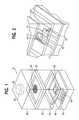
- FIG. 1shows an embodiment of an optical chassis 5 of the present invention having four substrates. These four substrates include a mount substrate 10 , a spacer substrate 20 , a sealer substrate 30 and an optional optics substrate 40 .
- the mount substrate 10serves as a mount for optoelectronic devices, here a light source 12 and a power monitor 14 , and provides the electrical interconnections, here including a wire bond 16 , conductive patterns 17 and metalized trenches 18 .
- the conductive patterns 17each include a pad for the wire bond 16 and connect the pad to the trench 18 for external communication.
- the conductive patterns 17may be created by patterning conductive material on the mount substrate 10 in a known manner.
- the trenches 18may be created by removing a portion of the mount substrate 10 in a conventional manner and filling this portion with conductive material.
- the conductive material for the trenches 18may be provided at the same time the conductive patterns 17 are formed.
- the details of the mount substrate 10can be seen more clearly in FIG. 2 .
- the spacer substrate 20provides room for the beam output from the light source 12 to expand. If the optoelectronic device 12 does not have its active area on its top face, e.g., an edge emitting laser, an appropriate portion of a sidewall 22 of the spacer substrate 20 may be angled and coated with a reflective coating to appropriately direct the beam in the optical chassis 5 .
- a hole 24 in the spacer wafer 20may be formed by etching a silicon wafer, producing the characteristic angled sidewall 22 from such an etch.
- the spacer substrate 20in conjunction with the sealer substrate 30 , hermetically seals and protects the optoelectronic devices 12 , 14 from the environment.
- the sealer substrate 30may also include an optical element on either surface thereof, e.g., an optical element which reduces the divergence of the beam output from the light source 12 .
- the optional optics substrate 40includes at least one optical element.
- a diffractive optical element 44 on a first surface of the optics substrate 40directs some of the light from the light source 12 to the power monitor 14 , as disclosed, for example, in commonly assigned U.S. Pat. No. 6,314,223 entitled “Diffractive Vertical Cavity Surface Emitting Laser Power Monitor and System.”
- a coupling element 42 on a second surface of the optics substrate 40may couple the light between the optoelectronic device, here the light source 12 , and further applications, e.g., a fiber.
- more than one functionalitymay be incorporated into each optical element.
- a separation feature 32e.g., an indentation or stand off, may be provided on either the sealer substrate 30 or the optional optics substrate 40 to insure proper functioning of the optical element.
- the sealer substrate 30is transparent.
- the sealer substrate 30may be glass or may be some other transparent material that closely matches the coefficient of thermal expansion of the spacer substrate 20 , e.g., Pyrex when the spacer substrate is silicon.
- the smaller size of the chassis 5e.g., roughly 2 mm by 2 mm in x and y, also helps with any thermal mismatch, since there is not a lot of strain placed in the securing joints between the substrates.
- mating featuresmay be provided on a terminal surface thereof.
- a standoff 43encircling the optical element 42 may be provided.
- the standoff 43may be SU-8 and provides both alignment of the optical chassis 5 with additional devices and provides separation of the optical element 42 .
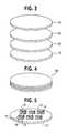
- a plurality of each of these substratesmay be created on a wafer level, secured together with other substrates in a vertical stack, and then vertically separated to form a plurality of individual optical chassis 5 .
- a mount wafer 10 ′, a spacer wafer 20 ′, a sealer wafer 30 ′ and an optional optics wafer 40 ′are to be aligned and secured together on a wafer level.
- Each of these wafersincludes a plurality of the respective mount substrates 10 , spacer substrates 20 , sealer substrates 30 and optional optical substrates 40 .
- the top three wafers 40 ′, 30 ′ and 20 ′may be created completely on a wafer level in known fashions. These wafers may then be secured together as shown in FIG. 4 forming a secured stack wafer 50 ′. These wafers may be aligned and secured as set forth, for example, in U.S. Pat. No. 6,096,155 entitled “Method of Dicing Wafer Level Integrated Optical Elements.”
- a plurality of metalized trenches 18 for providing the electrical interconnectionsmay be formed on the wafer level.
- the optoelectronic elements 12 , 14may then be positioned on the mount wafer 10 ′, e.g., using pick-and-place techniques, and then wire bonded 16 to the metalized trenches 18 .
- the metalized trenches 18may extend along the mount wafer 10 ′, so the separation of the mount wafer 10 ′ will expose the metal on the edge of the mount substrate, as can be seen in FIGS. 1 and 2 .
- the secured stack wafer 50 ′is then secured to the mount wafer 10 ′ and then vertically separated to form a plurality of optical chassis 5 as shown in FIG. 1 .
- the secured stack wafermay be vertically separated to form secured stack substrates, which are then bonded to the mount wafer 10 ′.
- FIGS. 6 and 7An alternative optical chassis 55 is shown in FIGS. 6 and 7 .
- the optional optical substrate 40is not included. Only a diffractive optical element 34 for power monitoring and/or efficient coupling is provided on the sealer substrate 30 .
- the spacer substrate 20is the same as in FIG. 1 .
- the mount substrate 60provides different electrical connections as in FIG. 1 for the light source 12 and the power monitor 14 .
- the optoelectronic devicesare again wire bonded, here to conductive pads 65 .
- conductivee.g., metalized, through holes or vias 64 and conductive structures 62 , e.g., solder balls, are used to provide the electrical interconnections to the electrooptical elements on the top surface of the mount substrate 60 .
- conductive structuresmay be large enough to obscure the hole in the mount substrate to insure the seal, to avoid creating a thermal gradient and to avoid extra oxidation. This solution may be particularly useful if the mount substrate is a ceramic, since it is expensive to put solder on ceramic.
- the sealmay be hermetic.
- FIGS. 8A-8DAnother alternative for providing electrical interconnections to the optoelectronic element on a wafer level is shown in FIGS. 8A-8D .
- a saw or other etching deviceis used to produce V-shaped groove 81 in a wafer 80 .
- the groove 81 and the wafer 80are coated with an electrically conductive coating 82 , e.g., metal, as shown in FIG. 8B .
- the wafer 80is separated at the V-groove 81 and at another portion to form a mount substrate 83 , as shown in FIG. 8C .
- the groove 81needs to be wide enough so that an angle remains after separation. For example, if dicing is used as the separation technique, the groove will need to be wider than the blade width of the dicing saw.
- an optoelectronic device 86is mounted on the conductive coating 82 of the mount substrate 83 .
- a solder ball 84 or other conductive structuremay then used to connect the conductive coating 82 to an electrical connection on a board 88 .
- the other substrates 20 , 30 and optionally 40may be stacked over the mount substrate 83 as shown in the other configurations.
- Electrical input/outputmay also be realized as shown in FIG. 9 , in which the substrates forming the optical chassis do not have the same width, thereby forming a ledge 15 , with the electrical connection being realized on a portion of the chassis 5 providing the ledge 15 .
- the ledge 15may be formed by having the mount substrate 10 extend further in at least one direction than the adjacent spacer substrate 20 .
- the electrical contactsmay be formed on the surface of the ledge or a portion of the ledge 15 may be removed to form the trenches 18 therein to increase the surface for electrical contact.
- Such a ledgemay be formed by die bonding a secured stacked substrate having the spacer substrate 20 and the sealer substrate 30 to the mount substrate 10 .
- Forming such a ledge on wafer levelmay be realized in a number of manners, including using dicing saws of different thicknesses and dicing through opposite surfaces, e.g., flipping the wafer after partial dicing, of the secured stacked wafer, including the mount wafer 10 ′. Details of forming such a ledge on a wafer level are set forth in the commonly assigned, co-pending application entitled “Separating of Optical Integrated Modules and Structures Formed Thereby,” filed Oct. 23, 2001, which is hereby incorporated by reference in its entirety.
- the optical chassis of the present inventionmay be used to simply replace the conventional TO-can element and can have the conventional optics aligned thereto, as is currently done for the TO-can optoelectronics. Two manners of achieving this are shown in shown in FIGS. 10 and 11 .
- the vertically integrated optical chassis 55 of the present inventionmay have an optical element 90 , including optical elements larger in the x- and/or y-direction than the optical chassis 55 , die-bonded thereto.
- the optical element 90may be separate from but aligned with the optical chassis 55 , here shown in a common housing 92 . This separation reduces the alignment tolerances for the optical element 90 .
- the sealer substrate 30may still include optics thereon for improving the light from the light source 12 , e.g., collimating or at least reducing the divergence of the light.
- FIGS. 12A-12BA specific configuration of an optical chassis in accordance with the present invention is shown in FIGS. 12A-12B .
- an optical chassis 100is attached to a flex lead 150 , inserted into a magnet 160 , on which a fiber stop 170 and then a fiber sleeve 180 is secured.
- This structuremay be provided on a heat sink.
- the optical chassis 100includes a mount substrate 110 having a ledge 115 , a spacer substrate 120 and a sealer substrate 130 .
- An optoelectronic device 112 and wire bonds 116are on the mount substrate 110 .
- the sealer substrate 130includes a lens 132 and an angled, reflective sidewall 122 .
- the angled, reflective sidewall 122serves as a mirror to direct light between the optoelectronic device 112 and the fiber in the fiber sleeve 180 . If the active area or facet of the optoelectronic device is not on an edge thereof, this angled, reflective sidewall 122 is not needed.
- An additional spacer substrate 136which may include additional spacing structures 138 , separates the lens 132 from an isolator stack 140 .
- the spacing structures 138are used when a passive optical element is on one or more opposing surfaces in the stack and the surfaces would otherwise contact the passive optical element.
- the spacing structuresmay be integral with the surface or may be provided on the surface. Alternatively, these spacing structures may be on the sealer substrate 130 .
- the electrical connection of the optoelectronic device 116is realized using the ledge 115 , as discussed in connection with FIG. 9 .
- the isolator stack 140includes a first polarizer 142 , a Faraday rotator 144 and a second polarizer 146 .
- the magnet 170which may be a ring magnet, surrounds the isolator stack 140 when the optical chassis 100 is inserted as shown in FIG. 12A , thereby completing the isolator. If the Faraday rotator 144 is a latching type, then the separate magnet 170 is not needed.
- the active elementsare secured to the mount substrate such that they remain secured and withstand subsequent processing, e.g., the securing of the substrate.
- the construction of the optical chassis of the present inventionneeds to be determined in an appropriate order, with the least robust technique being performed last.
- the materials used for the securing of the active elements, realizing the electrical connections and the securing of the substratesmust be selected in accordance with the required order.
- the active elementsmay be secured on the mount substrate using a gold-tin (AuSn) solder and the substrates may then be secured using a material with a lower melting point, e.g., silver-tin (AgSn) solder.
- FIGS. 13A-14BTechniques for realizing alignment of the optical elements in the optical chassis are shown in FIGS. 13A-14B .
- characteristicse.g., lens thickness, radius of curvature (ROC), of individual elements.
- ROCradius of curvature
- the variation in ROCmay be compensated for with the placement of the angled surface 122 of the spacer substrate 120 , as shown in FIG. 13A-13B .
- the separation d between the optoelectronic device 112 and a back edge of the angled surface 122is determined in accordance with the ROC of the lens to be used. If the angled surface 122 has an angle of approximately 45°, this distance d will be roughly equal to the height of the spacer substrate 120 . Thus, this aligning of the optoelectronic device 112 with the angled surface 122 compensates for any variations in the thickness of the spacer substrate 120 , as well as taking the ROC of the lens into account.
- the aligning of the lens to the optoelectronic device 112is shown in FIGS. 14A-14B .
- the image of the active area of the optoelectronic device 112 in the reflective angled surface 122may be used to align the lens.
- a bottom surface of the substrate having the lens thereonwhich may be the sealer substrate 130 as shown in FIGS. 12A-12B , includes alignment features 134 , here in the form of a crosshair centered on the lens on the top surface of the substrate.
- the alignment features 134are then centered with the image of the active area of the optoelectronic device 112 as reflected by the angled surface 122 to insure proper alignment there between. Since the height of the optoelectronic element changes its location on the angled surface 122 , by aligning the lens to the reflection from the angled surface 122 , variations in the height of the optoelectronic element may be compensated for as well.
- the lensmay be aligned by directly viewing the active area using alignment features 134 .
- the alignment thereofis not critical. Since the sealer substrate 130 is transparent, alignment features do not need to be provided thereon, as alignment features on surfaces below the sealer substrate may be viewed through it. If there are optical elements on other substrates, and the sealer substrate 130 is transparent, the same alignment techniques may be employed.
- the optical chassismay include a sealer substrate 230 , a spacer substrate 220 , and a mount substrate 260 .
- the sealer substrate 230 , the spacer substrate 220 and the mount substrate 260may form an enclosure 240 .
- the mount substrate 260is illustrated in FIG. 15 as being larger in the x-y plane than the sealer substrate 230 and the spacer substrate 220 , the mount substrate may be the same size in the x-y plane as the remaining substrates.
- the spacer substrate 220may be formed from a wafer, e.g., a silicon wafer, etc. or may be an adhesive, e.g., a punched adhesive, or simultaneously provided, as set forth, for example, in U.S. Pat. No. 6,669,803, which is hereby incorporated by reference in its entirety.
- the sealer substrate 230may include an optical element 232 on one or both surfaces in the x-y plane.
- the optical element(s)may provide an image onto the detector array 262 .
- n/2 substrates on the sealer substrate 230may provide up to n parallel surfaces on which optical elements may be created.
- An example of such an optics stack 270is illustrated in the schematic cross-sectional perspective view of FIG. 16 .
- the optics stack 270may have a same dimension in the x-y plane as the sealer substrate 230 or may be smaller or larger in the x-y plane than the sealer substrate 230 .
- the optics stack 270may include a first substrate 280 , a spacer 285 , and a second substrate 290 , thereby providing four parallel surfaces on which optical elements may be formed.
- the first substrate 280 , the spacer 285 and the second substrate 290may form interior space 295 .
- a first optical element 282is on an upper surface of first substrate 280 and a second optical element 292 is on an upper surface of the second substrate 290 , i.e., within the interior space 295 .
- the spacer 285may be integrated with one or both of the adjacent substrates, formed from a wafer, e.g., a silicon wafer, etc. or may be an adhesive, e.g., a punched adhesive, or simultaneously provided, as set forth, for example, in U.S. Pat. No. 6,669,803, which is hereby incorporated by reference in its entirety.
- the mount substrate 260may be a sensor substrate, and may include detector array 262 .
- the detector array 262may be in the enclosure 240 .
- the detector array 262may be a CMOS photodiode array, i.e., may be monolithically integrated in the mount substrate 260 , which may be a CMOS IC substrate.
- the detector array 262may receive an image output from the optical element 232 .
- the mount substratemay further include an array of microlenses (not shown) on the detector array 262 .
- conductivee.g., metalized, through holes or vias (not seen in this view) and conductive structures 266 , e.g., solder balls, may be used to provide the electrical interconnections to the detector array 262 on the top surface of the mount substrate 260 .
- These through holesmay have any appropriate cross section.
- the sealer substrate 230 and the spacer substrate 220may be secured and singulated on the wafer level, with or without the optics stack 270 of FIG. 16 . Then, a plurality of resultant structure may be secured to a corresponding plurality of detector arrays mount substrates on the wafer level. The mount substrate may then be singulated to form the optical chassis 200 .
- any of the two adjacent substrates in the z directionmay be secured on a wafer level, with resultant structures secured to remaining substrate(s) on wafer level.
- the optics stack 270may be secured on a wafer level, and singulated, then the substrates forming the optical chassis 200 may be secured on a wafer level, a plurality of optics stacks 270 may be secured to the wafer level optical chassis, and then the optical chassis may be singulated to form individual optical chassis with the optics stacks 270 thereon.
- the mount substrate 260is larger in the x-y plane than the sealer substrate 230 and the spacer substrate 220 , illustrated in FIG. 15 , these may still be secured on a wafer level.
- a first singulation stepmay be used to expose an upper surface of the mount substrate 260 , then a second singulation step, which may be the same process or a different process as the first singulation step, may be used to form the individual optical chassis 200 .
- an optical chassis having a small form factormay be created at least partially on a wafer level, including electrical interconnections.
- the optical chassis of the present inventionalso provides a seal without requiring a TO can or other separate housing. Further, since substrates of the optical chassis are secured to one another, rather than to a carrier as in a TO can, better alignment can be maintained for longer.
- any of the electrical interconnections shownmay be used with any optical chassis embodiments.
- additional optical substrates or elements as neededmay be secured to the optical chassis.
- the optics stackmay be secured to any of the optics chassis.
- any of the configurations of the optical chassismay be created at least partially on a wafer level as discussed regarding FIGS. 3-5 .
Landscapes
- Physics & Mathematics (AREA)
- General Physics & Mathematics (AREA)
- Optics & Photonics (AREA)
- Solid State Image Pick-Up Elements (AREA)
Abstract
Description
Claims (17)
Priority Applications (1)
| Application Number | Priority Date | Filing Date | Title |
|---|---|---|---|
| US11/932,693US7961989B2 (en) | 2001-10-23 | 2007-10-31 | Optical chassis, camera having an optical chassis, and associated methods |
Applications Claiming Priority (5)
| Application Number | Priority Date | Filing Date | Title |
|---|---|---|---|
| US09/983,278US6798931B2 (en) | 2001-03-06 | 2001-10-23 | Separating of optical integrated modules and structures formed thereby |
| US45766403P | 2003-03-26 | 2003-03-26 | |
| US10/809,914US7224856B2 (en) | 2001-10-23 | 2004-03-26 | Wafer based optical chassis and associated methods |
| US11/783,530US7751659B2 (en) | 2001-10-23 | 2007-04-10 | Optical apparatus |
| US11/932,693US7961989B2 (en) | 2001-10-23 | 2007-10-31 | Optical chassis, camera having an optical chassis, and associated methods |
Related Parent Applications (1)
| Application Number | Title | Priority Date | Filing Date |
|---|---|---|---|
| US11/783,530Continuation-In-PartUS7751659B2 (en) | 2001-10-23 | 2007-04-10 | Optical apparatus |
Publications (2)
| Publication Number | Publication Date |
|---|---|
| US20080251707A1 US20080251707A1 (en) | 2008-10-16 |
| US7961989B2true US7961989B2 (en) | 2011-06-14 |
Family
ID=39852866
Family Applications (1)
| Application Number | Title | Priority Date | Filing Date |
|---|---|---|---|
| US11/932,693Expired - Fee RelatedUS7961989B2 (en) | 2001-10-23 | 2007-10-31 | Optical chassis, camera having an optical chassis, and associated methods |
Country Status (1)
| Country | Link |
|---|---|
| US (1) | US7961989B2 (en) |
Cited By (5)
| Publication number | Priority date | Publication date | Assignee | Title |
|---|---|---|---|---|
| US20100006784A1 (en)* | 2008-07-09 | 2010-01-14 | Michael Mack | Method and system for a light source assembly supporting direct coupling to an integrated circuit |
| US20100321564A1 (en)* | 2004-04-08 | 2010-12-23 | Feldman Michael R | Camera system and associated methods |
| US20140037247A1 (en)* | 2012-07-31 | 2014-02-06 | Sagi Varghese Mathai | Apparatus for use in optoelectronics having a sandwiched lens |
| US9417389B2 (en) | 2008-11-06 | 2016-08-16 | Luxtera, Inc. | Coupling optical signals into silicon optoelectronic chips |
| US20170031115A1 (en)* | 2015-07-29 | 2017-02-02 | Corning Optical Communications LLC | Wafer-level integrated opto-electronic module |
Families Citing this family (10)
| Publication number | Priority date | Publication date | Assignee | Title |
|---|---|---|---|---|
| US7224856B2 (en)* | 2001-10-23 | 2007-05-29 | Digital Optics Corporation | Wafer based optical chassis and associated methods |
| KR20090033070A (en)* | 2007-09-27 | 2009-04-01 | 엘지이노텍 주식회사 | Camera module |
| WO2010129460A1 (en) | 2009-05-03 | 2010-11-11 | Lensvector Inc. | Camera module with tolerance adjustment using embedded active optics |
| WO2011008443A2 (en)* | 2009-06-29 | 2011-01-20 | Lensvector Inc. | Wafer level camera module with active optical element |
| US9065991B2 (en) | 2010-11-04 | 2015-06-23 | Lensvector Inc. | Methods of adjustment free manufacture of focus free camera modules |
| US9634051B2 (en)* | 2012-07-17 | 2017-04-25 | Heptagon Micro Optics Pte. Ltd. | Optical devices, in particular computational cameras, and methods for manufacturing the same |
| JPWO2017179144A1 (en)* | 2016-04-13 | 2019-02-21 | オリンパス株式会社 | Method of manufacturing optical unit for endoscope and endoscope |
| US10824054B2 (en) | 2017-01-24 | 2020-11-03 | Lg Electronics Inc. | Mobile terminal |
| WO2018139790A1 (en)* | 2017-01-24 | 2018-08-02 | 엘지전자 주식회사 | Mobile/portable terminal |
| KR102780349B1 (en)* | 2020-05-20 | 2025-03-12 | 삼성전자주식회사 | Probe card test apparatus |
Citations (37)
| Publication number | Priority date | Publication date | Assignee | Title |
|---|---|---|---|---|
| US4873566A (en)* | 1985-10-28 | 1989-10-10 | American Telephone And Telegraph Company | Multilayer ceramic laser package |
| US4945400A (en) | 1988-03-03 | 1990-07-31 | At&T Bell Laboratories | Subassembly for optoelectronic devices |
| US5011256A (en) | 1988-10-28 | 1991-04-30 | E. I. Du Pont De Nemours And Company | Package for an opto-electronic component |
| US5406543A (en)* | 1993-04-07 | 1995-04-11 | Olympus Optical Co., Ltd. | Optical head with semiconductor laser |
| US5668033A (en) | 1995-05-18 | 1997-09-16 | Nippondenso Co., Ltd. | Method for manufacturing a semiconductor acceleration sensor device |
| EP0881671A2 (en) | 1997-05-28 | 1998-12-02 | Matsushita Electric Industrial Co., Ltd. | Method for fabricating semiconductor device |
| US5926696A (en) | 1994-01-12 | 1999-07-20 | Lucent Technologies Inc. | Ball grid array plastic package |
| EP0975072A2 (en) | 1998-07-22 | 2000-01-26 | Canon Kabushiki Kaisha | Apparatus with an optical functional device having a special wiring electrode and method for fabricating the same |
| WO2000011714A1 (en) | 1998-08-25 | 2000-03-02 | Commissariat A L'energie Atomique | Collective method for conditioning a plurality of components initially formed in a common substrate |
| US6096155A (en) | 1996-09-27 | 2000-08-01 | Digital Optics Corporation | Method of dicing wafer level integrated multiple optical elements |
| US6102068A (en)* | 1997-09-23 | 2000-08-15 | Hewlett-Packard Company | Selector valve assembly |
| US6104690A (en)* | 1996-09-27 | 2000-08-15 | Digital Optics Corporation | Integrated optical apparatus and associated methods |
| US6150188A (en) | 1998-02-26 | 2000-11-21 | Micron Technology Inc. | Integrated circuits using optical fiber interconnects formed through a semiconductor wafer and methods for forming same |
| US6249136B1 (en) | 1999-06-28 | 2001-06-19 | Advanced Micro Devices, Inc. | Bottom side C4 bumps for integrated circuits |
| US20010010702A1 (en)* | 2000-02-02 | 2001-08-02 | Koichiro Tanaka | Beam homogenizer, laser irradiation apparatus, semiconductor device, and method of fabricating the semiconductor device |
| WO2001061748A1 (en) | 2000-02-16 | 2001-08-23 | Nova Crystals, Inc. | Method for fabricating light emitting diodes |
| EP1130646A1 (en) | 2000-02-29 | 2001-09-05 | Agilent Technologies Inc. a Delaware Corporation | Chip-mounted enclosure |
| US20020094528A1 (en)* | 2000-11-29 | 2002-07-18 | Salafsky Joshua S. | Method and apparatus using a surface-selective nonlinear optical technique for detection of probe-target interations |
| US20020126940A1 (en)* | 2001-03-06 | 2002-09-12 | Kathman Alan D. | Separating of optical integrated modules and structures formed thereby |
| US6472758B1 (en) | 2000-07-20 | 2002-10-29 | Amkor Technology, Inc. | Semiconductor package including stacked semiconductor dies and bond wires |
| US20020176459A1 (en)* | 2001-05-25 | 2002-11-28 | Martinsen Robert Jens | Method and apparatus for controlling thermal variations in an optical device |
| US20030002809A1 (en)* | 1998-06-08 | 2003-01-02 | Jian Benjamin B. | Vertically integrated optical devices coupled to optical fibers |
| US6509807B1 (en)* | 1997-04-08 | 2003-01-21 | X2Y Attenuators, Llc | Energy conditioning circuit assembly |
| US20030020091A1 (en)* | 2001-07-25 | 2003-01-30 | Motorola, Inc. | Structure and method for fabricating an optical switch utilizing the formation of a compliant substrate |
| US6606011B2 (en)* | 1998-04-07 | 2003-08-12 | X2Y Attenuators, Llc | Energy conditioning circuit assembly |
| US20030162214A1 (en)* | 1993-11-01 | 2003-08-28 | Nanogen, Inc. | Self-addressable self-assembling microelectronic systems and devices for molecular biological analysis and diagnostics |
| US20030222223A1 (en)* | 2002-06-03 | 2003-12-04 | Toshihiro Kamei | Solid-state detector and optical system for microchip analyzers |
| US20040077121A1 (en)* | 2002-04-22 | 2004-04-22 | Hiroshi Maeda | Solid-state imaging device and method of manufacturing said solid-state imaging device |
| US20040113549A1 (en)* | 2001-01-31 | 2004-06-17 | Roberts John K | High power radiation emitter device and heat dissipating package for electronic components |
| US20050225654A1 (en)* | 2004-04-08 | 2005-10-13 | Digital Optics Corporation | Thin color camera |
| US6969204B2 (en) | 2002-11-26 | 2005-11-29 | Hymite A/S | Optical package with an integrated lens and optical assemblies incorporating the package |
| US20060113622A1 (en)* | 2004-11-30 | 2006-06-01 | International Business Machines Corporation | A damascene copper wiring image sensor |
| US20070126898A1 (en)* | 2004-09-27 | 2007-06-07 | Digital Optics Corporation | Thin camera and associated methods |
| US7262073B2 (en)* | 2004-09-11 | 2007-08-28 | Samsung Electronics Co., Ltd. | CMOS image sensor and method of manufacturing same |
| US20080118241A1 (en)* | 2006-11-16 | 2008-05-22 | Tekolste Robert | Control of stray light in camera systems employing an optics stack and associated methods |
| US20080136956A1 (en)* | 2006-11-17 | 2008-06-12 | Tessera North America | Internal noise reducing structures in camera systems employing an optics stack and associated methods |
| US7714262B2 (en)* | 2005-07-01 | 2010-05-11 | Richard Ian Olsen | Digital camera with integrated ultraviolet (UV) response |
Family Cites Families (1)
| Publication number | Priority date | Publication date | Assignee | Title |
|---|---|---|---|---|
| DE10027008B4 (en)* | 2000-05-31 | 2016-12-29 | Robert Bosch Gmbh | metering |
- 2007
- 2007-10-31USUS11/932,693patent/US7961989B2/ennot_activeExpired - Fee Related
Patent Citations (45)
| Publication number | Priority date | Publication date | Assignee | Title |
|---|---|---|---|---|
| US4873566A (en)* | 1985-10-28 | 1989-10-10 | American Telephone And Telegraph Company | Multilayer ceramic laser package |
| US4945400A (en) | 1988-03-03 | 1990-07-31 | At&T Bell Laboratories | Subassembly for optoelectronic devices |
| US5011256A (en) | 1988-10-28 | 1991-04-30 | E. I. Du Pont De Nemours And Company | Package for an opto-electronic component |
| US5406543A (en)* | 1993-04-07 | 1995-04-11 | Olympus Optical Co., Ltd. | Optical head with semiconductor laser |
| US20030162214A1 (en)* | 1993-11-01 | 2003-08-28 | Nanogen, Inc. | Self-addressable self-assembling microelectronic systems and devices for molecular biological analysis and diagnostics |
| US5926696A (en) | 1994-01-12 | 1999-07-20 | Lucent Technologies Inc. | Ball grid array plastic package |
| US5668033A (en) | 1995-05-18 | 1997-09-16 | Nippondenso Co., Ltd. | Method for manufacturing a semiconductor acceleration sensor device |
| US6104690A (en)* | 1996-09-27 | 2000-08-15 | Digital Optics Corporation | Integrated optical apparatus and associated methods |
| US6096155A (en) | 1996-09-27 | 2000-08-01 | Digital Optics Corporation | Method of dicing wafer level integrated multiple optical elements |
| US6509807B1 (en)* | 1997-04-08 | 2003-01-21 | X2Y Attenuators, Llc | Energy conditioning circuit assembly |
| EP0881671A2 (en) | 1997-05-28 | 1998-12-02 | Matsushita Electric Industrial Co., Ltd. | Method for fabricating semiconductor device |
| US6184066B1 (en)* | 1997-05-28 | 2001-02-06 | Matsushita Electric Industrial Co., Ltd. | Method for fabricating semiconductor device |
| US6102068A (en)* | 1997-09-23 | 2000-08-15 | Hewlett-Packard Company | Selector valve assembly |
| US6150188A (en) | 1998-02-26 | 2000-11-21 | Micron Technology Inc. | Integrated circuits using optical fiber interconnects formed through a semiconductor wafer and methods for forming same |
| US6606011B2 (en)* | 1998-04-07 | 2003-08-12 | X2Y Attenuators, Llc | Energy conditioning circuit assembly |
| US6981804B2 (en)* | 1998-06-08 | 2006-01-03 | Arrayed Fiberoptics Corporation | Vertically integrated optical devices coupled to optical fibers |
| US20030002809A1 (en)* | 1998-06-08 | 2003-01-02 | Jian Benjamin B. | Vertically integrated optical devices coupled to optical fibers |
| US6597713B2 (en)* | 1998-07-22 | 2003-07-22 | Canon Kabushiki Kaisha | Apparatus with an optical functional device having a special wiring electrode and method for fabricating the same |
| EP0975072A2 (en) | 1998-07-22 | 2000-01-26 | Canon Kabushiki Kaisha | Apparatus with an optical functional device having a special wiring electrode and method for fabricating the same |
| WO2000011714A1 (en) | 1998-08-25 | 2000-03-02 | Commissariat A L'energie Atomique | Collective method for conditioning a plurality of components initially formed in a common substrate |
| US6581279B1 (en) | 1998-08-25 | 2003-06-24 | Commissariat A L'energie Atomique | Method of collectively packaging electronic components |
| US6249136B1 (en) | 1999-06-28 | 2001-06-19 | Advanced Micro Devices, Inc. | Bottom side C4 bumps for integrated circuits |
| US20010010702A1 (en)* | 2000-02-02 | 2001-08-02 | Koichiro Tanaka | Beam homogenizer, laser irradiation apparatus, semiconductor device, and method of fabricating the semiconductor device |
| US20020068373A1 (en)* | 2000-02-16 | 2002-06-06 | Nova Crystals, Inc. | Method for fabricating light emitting diodes |
| WO2001061748A1 (en) | 2000-02-16 | 2001-08-23 | Nova Crystals, Inc. | Method for fabricating light emitting diodes |
| EP1130646A1 (en) | 2000-02-29 | 2001-09-05 | Agilent Technologies Inc. a Delaware Corporation | Chip-mounted enclosure |
| US6472758B1 (en) | 2000-07-20 | 2002-10-29 | Amkor Technology, Inc. | Semiconductor package including stacked semiconductor dies and bond wires |
| US20020094528A1 (en)* | 2000-11-29 | 2002-07-18 | Salafsky Joshua S. | Method and apparatus using a surface-selective nonlinear optical technique for detection of probe-target interations |
| US20060244118A1 (en)* | 2001-01-31 | 2006-11-02 | Gentex Corporation | High power radiation emitter device and heat dissipating package for electronic components |
| US20040113549A1 (en)* | 2001-01-31 | 2004-06-17 | Roberts John K | High power radiation emitter device and heat dissipating package for electronic components |
| US20020126940A1 (en)* | 2001-03-06 | 2002-09-12 | Kathman Alan D. | Separating of optical integrated modules and structures formed thereby |
| US20020176459A1 (en)* | 2001-05-25 | 2002-11-28 | Martinsen Robert Jens | Method and apparatus for controlling thermal variations in an optical device |
| US20030020091A1 (en)* | 2001-07-25 | 2003-01-30 | Motorola, Inc. | Structure and method for fabricating an optical switch utilizing the formation of a compliant substrate |
| US20040077121A1 (en)* | 2002-04-22 | 2004-04-22 | Hiroshi Maeda | Solid-state imaging device and method of manufacturing said solid-state imaging device |
| US20030222223A1 (en)* | 2002-06-03 | 2003-12-04 | Toshihiro Kamei | Solid-state detector and optical system for microchip analyzers |
| US6969204B2 (en) | 2002-11-26 | 2005-11-29 | Hymite A/S | Optical package with an integrated lens and optical assemblies incorporating the package |
| US20050225654A1 (en)* | 2004-04-08 | 2005-10-13 | Digital Optics Corporation | Thin color camera |
| US7773143B2 (en)* | 2004-04-08 | 2010-08-10 | Tessera North America, Inc. | Thin color camera having sub-pixel resolution |
| US20070262366A1 (en)* | 2004-09-11 | 2007-11-15 | Samsung Electronics Co,. Ltd. | Cmos image sensor and method of manufacturing same |
| US7262073B2 (en)* | 2004-09-11 | 2007-08-28 | Samsung Electronics Co., Ltd. | CMOS image sensor and method of manufacturing same |
| US20070126898A1 (en)* | 2004-09-27 | 2007-06-07 | Digital Optics Corporation | Thin camera and associated methods |
| US20060113622A1 (en)* | 2004-11-30 | 2006-06-01 | International Business Machines Corporation | A damascene copper wiring image sensor |
| US7714262B2 (en)* | 2005-07-01 | 2010-05-11 | Richard Ian Olsen | Digital camera with integrated ultraviolet (UV) response |
| US20080118241A1 (en)* | 2006-11-16 | 2008-05-22 | Tekolste Robert | Control of stray light in camera systems employing an optics stack and associated methods |
| US20080136956A1 (en)* | 2006-11-17 | 2008-06-12 | Tessera North America | Internal noise reducing structures in camera systems employing an optics stack and associated methods |
Cited By (15)
| Publication number | Priority date | Publication date | Assignee | Title |
|---|---|---|---|---|
| US8953087B2 (en)* | 2004-04-08 | 2015-02-10 | Flir Systems Trading Belgium Bvba | Camera system and associated methods |
| US20100321564A1 (en)* | 2004-04-08 | 2010-12-23 | Feldman Michael R | Camera system and associated methods |
| US8440989B2 (en)* | 2008-07-09 | 2013-05-14 | Luxtera Inc. | Method and system for a light source assembly supporting direct coupling to an integrated circuit |
| US20100006784A1 (en)* | 2008-07-09 | 2010-01-14 | Michael Mack | Method and system for a light source assembly supporting direct coupling to an integrated circuit |
| US8168939B2 (en)* | 2008-07-09 | 2012-05-01 | Luxtera, Inc. | Method and system for a light source assembly supporting direct coupling to an integrated circuit |
| US10234646B2 (en) | 2008-07-09 | 2019-03-19 | Luxtera, Inc. | Light source assembly supporting direct coupling to an integrated circuit |
| US9417389B2 (en) | 2008-11-06 | 2016-08-16 | Luxtera, Inc. | Coupling optical signals into silicon optoelectronic chips |
| US9684128B2 (en) | 2008-11-06 | 2017-06-20 | Luxtera, Inc. | Method and system for coupling optical signals into silicon optoelectronics chips |
| US9904012B2 (en) | 2008-11-06 | 2018-02-27 | Luxtera, Inc. | Coupling optical signals into silicon optoelectronic chips |
| US10185086B2 (en) | 2008-11-06 | 2019-01-22 | Luxtera, Inc. | Method and system for coupling optical signals into silicon optoelectronic chips |
| US10451801B2 (en) | 2008-11-06 | 2019-10-22 | Luxtera, Inc. | Method and system for coupling optical signals into silicon optoelectronic chips |
| US20140037247A1 (en)* | 2012-07-31 | 2014-02-06 | Sagi Varghese Mathai | Apparatus for use in optoelectronics having a sandwiched lens |
| US8934745B2 (en)* | 2012-07-31 | 2015-01-13 | Hewlett-Packard Development Company, L.P. | Apparatus for use in optoelectronics having a sandwiched lens |
| US20170031115A1 (en)* | 2015-07-29 | 2017-02-02 | Corning Optical Communications LLC | Wafer-level integrated opto-electronic module |
| US10082633B2 (en)* | 2015-07-29 | 2018-09-25 | Corning Optical Communications LLC | Wafer-level integrated opto-electronic module |
Also Published As
| Publication number | Publication date |
|---|---|
| US20080251707A1 (en) | 2008-10-16 |
Similar Documents
| Publication | Publication Date | Title |
|---|---|---|
| US7961989B2 (en) | Optical chassis, camera having an optical chassis, and associated methods | |
| US7751659B2 (en) | Optical apparatus | |
| US8803269B2 (en) | Wafer scale packaging platform for transceivers | |
| US9442255B2 (en) | Low profile fiber-to-module interface with relaxed alignment tolerances | |
| JP5086521B2 (en) | Optical receiver package | |
| US9465176B2 (en) | Small form factor transceiver compatible with solder processing | |
| CN100530865C (en) | Surface emitting laser package having integrated optical element and alignment post | |
| US9151916B2 (en) | Compact optical package made with planar structures | |
| US20160291269A1 (en) | Photonic integrated circuit chip packaging | |
| US6533471B2 (en) | Optical subassembly | |
| US9507112B2 (en) | Photoelectric conversion module and method of manufacturing photoelectric conversion module | |
| JP3532456B2 (en) | Semiconductor device having optical signal input / output mechanism | |
| JP4969775B2 (en) | Optical device package having reflector and alignment post | |
| US6643420B2 (en) | Optical subassembly | |
| JP4728625B2 (en) | Optical semiconductor device and optical module using the same | |
| CA2523418C (en) | Package for optoelectronic device on wafer level and associated methods | |
| US7141871B2 (en) | Method for manufacturing encapsulated opto-electronic devices and encapsulated device thus obtained | |
| US7375315B2 (en) | Integrated optical transceiver and related methods | |
| US7842914B2 (en) | Optoelectronic package, camera including the same and related methods | |
| TW202527046A (en) | Integrated optoelectronic module |
Legal Events
| Date | Code | Title | Description |
|---|---|---|---|
| AS | Assignment | Owner name:TESSERA NORTH AMERICA, NORTH CAROLINA Free format text:ASSIGNMENT OF ASSIGNORS INTEREST;ASSIGNORS:KATHMAN, ALAN D.;MORRIS, JAMES E.;HAMMOND, JOHN BARNETT;AND OTHERS;REEL/FRAME:020483/0121;SIGNING DATES FROM 20080104 TO 20080116 Owner name:TESSERA NORTH AMERICA, NORTH CAROLINA Free format text:ASSIGNMENT OF ASSIGNORS INTEREST;ASSIGNORS:KATHMAN, ALAN D.;MORRIS, JAMES E.;HAMMOND, JOHN BARNETT;AND OTHERS;SIGNING DATES FROM 20080104 TO 20080116;REEL/FRAME:020483/0121 | |
| STCF | Information on status: patent grant | Free format text:PATENTED CASE | |
| AS | Assignment | Owner name:DIGITALOPTICS CORPORATION, CALIFORNIA Free format text:ASSIGNMENT OF ASSIGNORS INTEREST;ASSIGNOR:DIGITALOPTICS CORPORATION EAST;REEL/FRAME:031888/0371 Effective date:20131112 | |
| AS | Assignment | Owner name:DIGITALOPTICS CORPORATION EAST, NORTH CAROLINA Free format text:CHANGE OF NAME;ASSIGNOR:TESSERA NORTH AMERICA, INC.;REEL/FRAME:032590/0399 Effective date:20110701 | |
| FPAY | Fee payment | Year of fee payment:4 | |
| AS | Assignment | Owner name:NAN CHANG O-FILM OPTOELECTRONICS TECHNOLOGY LTD, C Free format text:ASSIGNMENT OF ASSIGNORS INTEREST;ASSIGNORS:DIGITALOPTICS CORPORATION;DIGITALOPTICS CORPORATION MEMS;FOTONATION LIMITED;REEL/FRAME:034883/0237 Effective date:20141114 | |
| AS | Assignment | Owner name:DIGITALOPTICS CORPORATION, CALIFORNIA Free format text:CORRECTIVE ASSIGNMENT TO CORRECT THE FILING DATE INSIDE AN ASSIGNMENT. PREVIOUSLY RECORDED AT REEL: 031888 FRAME: 0371. ASSIGNOR(S) HEREBY CONFIRMS THE ASSIGNMENT;ASSIGNOR:DIGITALOPTICS CORPORATION EAST;REEL/FRAME:037629/0291 Effective date:20131112 | |
| FEPP | Fee payment procedure | Free format text:MAINTENANCE FEE REMINDER MAILED (ORIGINAL EVENT CODE: REM.); ENTITY STATUS OF PATENT OWNER: LARGE ENTITY | |
| LAPS | Lapse for failure to pay maintenance fees | Free format text:PATENT EXPIRED FOR FAILURE TO PAY MAINTENANCE FEES (ORIGINAL EVENT CODE: EXP.); ENTITY STATUS OF PATENT OWNER: LARGE ENTITY | |
| STCH | Information on status: patent discontinuation | Free format text:PATENT EXPIRED DUE TO NONPAYMENT OF MAINTENANCE FEES UNDER 37 CFR 1.362 | |
| FP | Lapsed due to failure to pay maintenance fee | Effective date:20190614 |