US7961511B2 - Hybrid programming methods and systems for non-volatile memory storage elements - Google Patents
Hybrid programming methods and systems for non-volatile memory storage elementsDownload PDFInfo
- Publication number
- US7961511B2 US7961511B2US11/535,452US53545206AUS7961511B2US 7961511 B2US7961511 B2US 7961511B2US 53545206 AUS53545206 AUS 53545206AUS 7961511 B2US7961511 B2US 7961511B2
- Authority
- US
- United States
- Prior art keywords
- programming
- cell
- writing
- programmed state
- volatile memory
- Prior art date
- Legal status (The legal status is an assumption and is not a legal conclusion. Google has not performed a legal analysis and makes no representation as to the accuracy of the status listed.)
- Active
Links
Images


Classifications
- G—PHYSICS
- G11—INFORMATION STORAGE
- G11C—STATIC STORES
- G11C11/00—Digital stores characterised by the use of particular electric or magnetic storage elements; Storage elements therefor
- G11C11/56—Digital stores characterised by the use of particular electric or magnetic storage elements; Storage elements therefor using storage elements with more than two stable states represented by steps, e.g. of voltage, current, phase, frequency
- G11C11/5621—Digital stores characterised by the use of particular electric or magnetic storage elements; Storage elements therefor using storage elements with more than two stable states represented by steps, e.g. of voltage, current, phase, frequency using charge storage in a floating gate
- G11C11/5628—Programming or writing circuits; Data input circuits
- G—PHYSICS
- G11—INFORMATION STORAGE
- G11C—STATIC STORES
- G11C16/00—Erasable programmable read-only memories
- G11C16/02—Erasable programmable read-only memories electrically programmable
- G11C16/04—Erasable programmable read-only memories electrically programmable using variable threshold transistors, e.g. FAMOS
- G11C16/0483—Erasable programmable read-only memories electrically programmable using variable threshold transistors, e.g. FAMOS comprising cells having several storage transistors connected in series
- G—PHYSICS
- G11—INFORMATION STORAGE
- G11C—STATIC STORES
- G11C16/00—Erasable programmable read-only memories
- G11C16/02—Erasable programmable read-only memories electrically programmable
- G11C16/06—Auxiliary circuits, e.g. for writing into memory
- G11C16/10—Programming or data input circuits
- G—PHYSICS
- G11—INFORMATION STORAGE
- G11C—STATIC STORES
- G11C16/00—Erasable programmable read-only memories
- G11C16/02—Erasable programmable read-only memories electrically programmable
- G11C16/06—Auxiliary circuits, e.g. for writing into memory
- G11C16/34—Determination of programming status, e.g. threshold voltage, overprogramming or underprogramming, retention
- G11C16/3418—Disturbance prevention or evaluation; Refreshing of disturbed memory data
Definitions
- the present inventionrelates generally to technology for programming memory devices. More particularly, the present invention relates to a hybrid approach to the programming of non-volatile memory devices, and particularly, flash memory devices.
- Non-volatile semiconductor memory devicesand in particular flash memory devices, are becoming increasingly popular means of storage for small devices such as digital cameras, MP3 players, cellular telephones, personal digital assistants (PDAs), laptop computers, etc.
- Other forms of nonvolatile memoryinclude EPROM (Electrically Programmable Read Only Memory) and EEPROM (Electrically Erasable and Programmable Read Only Memory.
- flash memory cell transistorscontain a floating gate that is electrically isolated and located between a control gate and typically a p-type substrate. Programming of a memory cell results in raising the threshold value of the transistor to a positive value as a result of electrons being injected through the insulating dielectric layer into the floating gate. Conversely, erasing results in lowering the threshold value of the transistor to a negative value as a result of electrons being removed from the floating gate. In this manner, the threshold value of the memory cell indicates its corresponding logic state. Programming is generally accomplished by using one of three major mechanisms: Fowler-Nordheim (FN) tunneling, source side [hot-electron] injection (SSI) and channel, or substrate, hot-electron injection (CHEI or SHEI).
- FNFowler-Nordheim
- SSIsource side [hot-electron] injection
- CHEI or SHEIhot-electron injection
- EASBerased area self boosting
- Various techniqueshave improved the inhibition of program disturb, but still suffer from their own problems and fail to prevent program disturb in all instances. For example, in EASB, if the voltage applied to unselected wordlines is too low, channel boosting can be insufficient to prevent program disturb. Conversely, if this voltage is too high, there will be unintentional programming of memory cells on unselected wordlines as a result of tunneling.
- the three aforementioned techniquesalso suffer from a disturb mechanism that depends on whether or not the source-side neighbor cell is programmed. For example, if the source-side neighboring cell is programmed, it will have a negative charge on the floating gate.
- control gate of the source side neighboris at 0V, a highly reverse biased junction is created under the gate. This can lead to the phenomenon of GIDL resulting in a reduced boost potential, which can eventually lead to program disturb (in this case erasure). Conversely, if the source-side neighbor is erased, its threshold voltage is likely negative and the transistor of the cell may not turn off.
- wordline zero(WL 0 ) is particularly susceptible to certain program disturb mechanisms. This is a result of WL 0 being positioned adjacent to the source select gate (select gate source or SGS), which is typically held at 0V during many programming methods (such as FN Tunneling) by the SGS line. This has the effect of creating a high electric field across the source of the transistor on WL 0 which can cause program disturb
- an improved method of programming a non-volatile memory cell to a final programmed stateis described.
- the hybrid method describedis a more robust protocol suitable for reliably programming selected memory cells while eliminating programming disturbs.
- a hybrid method of programming a non-volatile memory cell to a final programmed statecomprises first programming the non-volatile memory cell to a first initial state according to a first initial programming mechanism. Subsequently, the non-volatile memory cell is programmed according to a second different programming mechanism thereby completing the programming of the non-volatile memory cell to the final programmed state.
- the first mechanismis a coarse mechanism capable of moving the threshold voltage distributions by large amounts using only a few programming pulses, while the second mechanism is enabled to fine-tune the distributions to their final desired states.
- the non-volatile memory cellis one of a number of non-volatile memory cells arranged to form a non-volatile memory array suitable for storing data.
- the non-volatile memory arrayis arranged in a NAND-type memory array architecture having a number of wordlines and bitlines.
- the described methodis contemplated for use on a multilevel type memory array that when programmed stores data in the form of at least one lower page and at least one associated upper page.
- the described methodis particularly advantageous for programming multilevel arrays where tighter more precisely positioned threshold voltage distributions are required.
- the first programming mechanismis used to program the lower page of the multilevel array and the second programming mechanism is used to program the upper page.
- the first programming mechanismis based on Fowler-Nordheim (FN) Tunneling, while the second programming mechanism is based on source side injection (SSI).
- FNFowler-Nordheim
- SSIsource side injection
- second programming mechanisms based on gate induced drain leakage (GIDL) and/or substrate hot electron injection (SHEI)are contemplated for use.
- the present inventionis especially pertinent to memory cells being programmed on wordline zero (WL 0 ).
- the hybrid methodis only employed to program WL 0 because memory cells on WL 0 are the most susceptible to program disturb mechanisms and, additionally, show the most improvement when programmed with the hybrid method of the present invention.
- FIG. 1illustrates an exemplary MOSFET having a floating gate.
- FIG. 2illustrates an exemplary non-volatile memory string.
- FIG. 3illustrates an exemplary non-volatile memory array.
- FIG. 4 aillustrates a plot of lower page threshold voltage states versus # of cells.
- FIG. 4 billustrates a plot showing the splitting of the lower page states of FIG. 4 a.
- FIG. 4 cillustrates a plot showing upper page states produced by splitting the lower page states of FIG. 4 a.
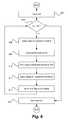
- FIG. 5shows a flowchart illustrating a hybrid algorithm of programming a non-volatile memory cell in accordance with an embodiment of the present invention.
- FIG. 6shows a flowchart illustrating a first method of programming a non-volatile memory cell in accordance with an embodiment of the present invention.
- FIG. 7shows a flowchart illustrating a second method of programming a non-volatile memory cell in accordance with an embodiment of the present invention.
- FIG. 8illustrates the memory cell of FIG. 1 under erase bias conditions in accordance with an embodiment of the present invention.
- FIG. 9illustrates a memory cell under FN tunneling programming bias conditions in accordance with an embodiment of the present invention.
- FIG. 10illustrates a memory cell under SSI programming bias conditions in accordance with an embodiment of the present invention.
- a memory cellis programmed according to two distinct programming mechanisms. The objective is to use a first programming mechanism that is fast, although course in its precision, to program the memory cell to a first state. Subsequently, a second slower, but much more precise, mechanism is used to fine-tune the memory cell to a final programmed state.
- the non-volatile memory storage systemis a flash memory chip having a NAND architecture, although the present invention is applicable to other forms of non-volatile memory including EPROM and EEPROM, and additionally to NOR architectures as well.
- the arrayconsists of non-volatile memory storage elements that are p-type substrate floating gate MOSFETs.
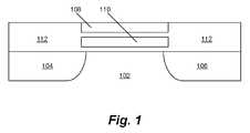
- FIG. 1illustrates an exemplary floating gate MOSFET, such as that used in this architecture, having a substrate 102 , a source 104 , a drain 106 , a control gate 108 , a floating gate 110 , and a dielectric 112 surrounding the floating gate.
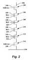
- NAND flash memorya number of such transistors, also known hereafter as cells, memory cells or memory storage elements, are arranged in series. On either side of the series of memory cells is an additional transistor known as a select transistor, or gate. Collectively, the memory cells and two select gates are referred to as a NAND string. By way of illustration, the equivalent circuit of a 4-transistor NAND string is illustrated in FIG. 2 . The four memory cells are labeled 206 , 208 , 210 and 212 .
- the first select gate 204referred to as the select gate drain (SGD), connects the NAND string to bitline 202 .
- SGDselect gate drain
- the second select gate 214connects the NAND string to sourceline 216 .
- Select gates 204 and 214are controlled by control gates 218 and 236 , respectively.
- An SGD linecontrols the control gate 218 for the select gate 204
- an SGS linecontrols the control gate 236 for the select gate 214 .
- the four series transistors 206 - 212each have both a control gate and a floating gate.
- transistor 206has a control gate 220 and a floating gate 222 ; transistor 208 has a control gate 224 and a floating gate 226 ; transistor 210 has a control gate 228 and a floating gate 230 ; and transistor 212 has a control gate 232 and a floating gate 234 .
- Control gates 220 , 224 , 228 and 232are connected to wordlines WL 3 , WL 2 , WL 1 and WL 0 , respectively. It should be noted that although the example provided describes a NAND string that includes four memory cells, other numbers of cells may be arranged in series and are permissible as well.
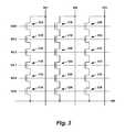
- FIG. 3illustrates an example of a NAND string array showing three NAND strings 301 , 302 and 303 of a memory array having many more NAND strings not shown.
- each of the NAND strings of FIG. 3includes two select gates and four memory cells.
- NAND string 301includes select gates 304 and 314 as well as memory cells 306 , 308 , 310 and 312 .
- NAND string 302includes select gates 316 and 326 as well as memory cells 318 , 320 , 322 and 324 .
- NAND string 303includes select gates 328 and 338 as well as memory cells 330 , 332 , 334 and 336 .
- control gates in a given row, or wordlineare connected.
- WL 0connects the control gates of memory cells 312 , 324 and 336 .
- Each of the NAND stringsare also connected to the same sourceline via select gates 314 , 326 and 338 .
- the SGS linecontrols the source side select gates 314 , 326 , and 338
- the SGD linecontrols the select gates 304 , 316 and 328 , which connect the NAND strings to their respective bitlines.
- a MLCis a non-volatile memory chip capable of storing multiple bits of data at a single memory cell location.
- each memory cell of an MLCis generally no different than that used in a conventional non-volatile memory chip, the difference laying in the programming of each memory cell.
- itis the level of the threshold voltage that distinguishes one logic state from another.
- each memory cellcan be programmed into one of four possible threshold voltage levels.
- a first programming passpositions the threshold voltage of the cell into one of two states. Collectively, these states are referred to as a lower page.
- a second programming passis then enabled to split one of the two aforementioned states by shifting the threshold voltage level to further program the cell.
- these four possible secondary statesare referred to as an upper page.
- the threshold voltage levels in an MLCneed to be more finely tuned than those in a standard memory chip, thereby rendering the multilevel chip more susceptible to programming disturbs.
- the disturbmay be severe enough such that only two states (i.e., a single bit) may be stored because the upper page states overlap and/or cannot be reliably distinguished from the lower page, as can be appreciated through examining FIG. 4 that illustrates three plots of threshold voltage distributions such as that may be observed in a 4LC.
- the lower page states 402 and 404 illustrated in FIG. 4 acorrespond to the erased (logic 1) distribution and programmed (logic 0) distribution, respectively.
- FIG. 4 billustrates a midway point in a second pass of programming in which midway distributions 406 , 408 , 410 and 412 are formed as the distributions 402 and 404 are being split into final programmed upper pages.
- FIG. 4 cillustrates the final (sufficiently distributed) upper page states E 414 , A 416 , B 418 and C 420 representing logic 11, 10, 01, and 00, respectively, produced by splitting and shifting the lower page states.
- a hybrid method of programming a non-volatile memory storage elementis described that substantially reduces the likelihood of programming disturb events especially with regards to wordline zero.
- a selected block of memory cellsis erased.
- the substrates of selected memory cells to be erasedare raised to a large positive erase voltage (i.e. 16V) while the wordlines corresponding to the selected cells are simultaneously grounded and sources and bit-lines are floated.
- FIG. 8illustrates the erase operation, in which arrows 802 and 804 indicate electron flows of the electrons 806 stored in the floating gate 110 .
- a first pattern of desired states for selected cells within a page of the blockis loaded.
- the programming algorithmthen proceeds to step 506 , where a first programming mechanism is used to program selected cells within the page.
- the programming operationis carried out using Fowler-Nordheim (FN) tunneling to initially program the selected memory cells.
- FNFowler-Nordheim
- a second pattern of desired statesis loaded.
- the programming operation of the memory cellis then completed by way of a second programming mechanism at step 510 that brings the selected memory cells to final programmed states.
- the second mechanismis based on using SSI to program the selected memory cells.
- GIDL or CHEI (SHEI) mechanismsmay be used as the second mechanism.
- the second mechanismmay also involve a combination of SSI, GIDL and CHEI.
- the first and second programming mechanismsmay be applied in any combination.
- the first mechanismis used to program a lower page of the memory chip while the second mechanism is used to program an upper page.
- This embodimentis preferred on one hand because the upper and lower pages are programmed during separate programming passes regardless of the algorithm, and thus, this provides a natural break in which to switch methods, but furthermore, programming of the lower page doesn't generally require the fine-tuning of the Vt distributions that is required when programming an upper page of an MLC.
- WL 0is programmed using the hybrid method described herein. There are a few reasons for this, one of which is that it has been observed that WL 0 is the most susceptible to certain program disturbs.
- SSIis used to program the upper page of WL 0 . It is easier to employ the SSI mechanism on WL 0 than it is on the other wordlines because, for the case of WL 0 , the voltage required for SSI is fairly well known. The reason for this is that the SGS isn't programmed, and hence, it has a fairly fixed Vt.
- FIG. 6shows a flowchart illustrating a method of programming using FN tunneling.
- the cellis subjected to a read operation 602 .
- the threshold voltage of the memory cellis verified.
- a program voltagei.e. 15V
- step 610unselected bitlines are pre-charged to a high voltage, generally Vdd, while, in step 612 , unselected wordlines are held at a passing voltage, Vpass, and the SGS is held at 0V.
- Vpgm and Vpassare incremented in step 614 and the process is repeated until the condition 604 is satisfied. It should be noted that other biasing schemes for programming with FN tunneling are well known in the art and are permitted as well.
- FIG. 9The bias conditions described above for programming with FN tunneling are illustrated in FIG. 9 , where a selected memory cell 904 on WL 0 is being programmed. Adjacent to the cell 904 are a select gate source 902 connected to an SGS line and a second memory cell 906 connected to WL 1 . The arrows 908 and 910 indicate the direction the electrons 912 are traveling. FIG. 9 also clearly shows why WL 0 is particularly susceptible to program disturb. With a large Vpgm (i.e. as high as 25 V) being applied to the selected cell and the SGS line being grounded, a large electric field is created in the n+ region between the two transistors. These electrons may, in turn, be injected into the floating gate of the selected memory cell. In contrast, when programming other memory cells on other wordlines besides WL 0 , the regions between the transistors don't typically experience such high fields because the neighboring cells will typically not be grounded.
- Vpgmi.e. as high as 25 V
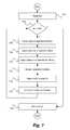
- FIG. 7shows a flowchart illustrating a method of programming using SSI.
- SSIis a method of programming whereby electrons are injected from the drain of one transistor into the gate above the source of an adjacent transistor.
- many of the bitline bias sensesare reversed with respect to FN tunneling.
- the cellis first subjected to a read operation 702 .
- the threshold voltage of the memory cellis verified.
- step 704it is then determined whether or not a second target verification voltage level, Vt 2 , is reached. If the threshold voltage of the memory cell is greater than Vt 2 , the cell is locked-out in step 718 .
- a high positive program voltage, Vpgmis applied to the control gate of the selected memory cell by biasing the appropriate wordline while, in step 708 , a high bias (4-5 V) is applied to the selected bitline.
- unselected wordlinesare held at a passing voltage, Vpass, while, in step 712 , unselected bitlines are grounded.
- the SGS lineis ramped from 0V until the threshold voltage of the select gate source is surpassed. It is around this threshold voltage that SSI begins. It should be noted that the SGS line is ramped so as to guarantee that the bias supplied to the SGS passes Vt.
- the floating gate of the selected cell on WL 0serves as a collector of electrons and the SGS serves as the injector.
- Vpgm and Vpassare incremented in step 716 and the process is repeated until the condition 704 is satisfied.
- FIG. 10The bias conditions described above for SSI programming are illustrated in FIG. 10 , where a selected memory cell 1004 on WL 0 is being programmed. Adjacent to the cell 1004 are a select gate source 1002 connected to an SGS line and a second memory cell 1006 connected to WL 1 . The arrows 1008 and 1010 indicate the direction the electrons 1012 are traveling. When the source select gate is ramped through its Vt, a conducting channel of electrons is created between its source and drain. Since the unselected wordlines are held at a passing voltage, the bias applied to the selected bitline draws electrons from the select gate source into the source of the selected memory cell 1004 . The large Vpgm applied to the control gate of cell 1004 causes electrons in the source to be injected into the floating gate of the cell 1004 .
- boost-based schemesfor boosting the channel voltage in a selected memory cell.
- the selected wordlineis often biased to Vdd while unselected wordlines are biased with a voltage, Vboost, which is greater than Vpass.
- Vboosta voltage
- Such boosting schemestake advantage of the channel capacitance of unselected cells.
- the strength of boostingincreases as the number of wordlines increases and scales down as the device geometries scale down.
- the much larger BL capacitancecan be used to provide the boost.
- SSIis very efficient in generating hot electrons in the channel of the selected transistor receiving the electrons and also provides very high efficiency in collecting these channel hot electrons into the floating gate. SSI also requires significantly less current than other modes of programming, improves reliability and allows for re-programming using on-chip charge pumps.
- the inventionmay be implemented in many other forms without departing from the spirit or scope of the invention.
- the inventionmay be implemented as a device that includes computer code stored on a computer readable medium for using a first programming mechanism to program a non-volatile memory cell to a first programmed state, and computer code stored on a computer readable medium for using a second programming mechanism to program the non-volatile memory cell from the first programmed state to a final programmed state.
Landscapes
- Engineering & Computer Science (AREA)
- Microelectronics & Electronic Packaging (AREA)
- Computer Hardware Design (AREA)
- Read Only Memory (AREA)
- Non-Volatile Memory (AREA)
- Semiconductor Memories (AREA)
Abstract
Description
Claims (3)
Priority Applications (3)
| Application Number | Priority Date | Filing Date | Title |
|---|---|---|---|
| US11/535,452US7961511B2 (en) | 2006-09-26 | 2006-09-26 | Hybrid programming methods and systems for non-volatile memory storage elements |
| PCT/US2007/078774WO2008039661A1 (en) | 2006-09-26 | 2007-09-18 | Hybrid programming methods and systems for non-volatile memory storage elements |
| TW096135598ATWI385664B (en) | 2006-09-26 | 2007-09-21 | Hybrid programming methods for non-volatile memory storage elements |
Applications Claiming Priority (1)
| Application Number | Priority Date | Filing Date | Title |
|---|---|---|---|
| US11/535,452US7961511B2 (en) | 2006-09-26 | 2006-09-26 | Hybrid programming methods and systems for non-volatile memory storage elements |
Publications (2)
| Publication Number | Publication Date |
|---|---|
| US20080084761A1 US20080084761A1 (en) | 2008-04-10 |
| US7961511B2true US7961511B2 (en) | 2011-06-14 |
Family
ID=38922699
Family Applications (1)
| Application Number | Title | Priority Date | Filing Date |
|---|---|---|---|
| US11/535,452ActiveUS7961511B2 (en) | 2006-09-26 | 2006-09-26 | Hybrid programming methods and systems for non-volatile memory storage elements |
Country Status (3)
| Country | Link |
|---|---|
| US (1) | US7961511B2 (en) |
| TW (1) | TWI385664B (en) |
| WO (1) | WO2008039661A1 (en) |
Cited By (2)
| Publication number | Priority date | Publication date | Assignee | Title |
|---|---|---|---|---|
| US20130170293A1 (en)* | 2011-12-28 | 2013-07-04 | Steven Sprouse | Hybrid multi-level cell programming sequences |
| US9158671B2 (en) | 2011-08-17 | 2015-10-13 | Samsung Electronics Co., Ltd. | Nonvolatile memory system with migration manager |
Families Citing this family (10)
| Publication number | Priority date | Publication date | Assignee | Title |
|---|---|---|---|---|
| US7944749B2 (en)* | 2006-12-21 | 2011-05-17 | Sandisk Corporation | Method of low voltage programming of non-volatile memory cells |
| US7623389B2 (en) | 2006-12-21 | 2009-11-24 | Sandisk Corporation | System for low voltage programming of non-volatile memory cells |
| US7894263B2 (en)* | 2007-09-28 | 2011-02-22 | Sandisk Corporation | High voltage generation and control in source-side injection programming of non-volatile memory |
| KR101468098B1 (en)* | 2008-06-23 | 2014-12-04 | 삼성전자주식회사 | Flash memory device and memory system including same |
| KR101569894B1 (en)* | 2008-11-12 | 2015-11-17 | 삼성전자주식회사 | Program method of nonvolatile memory device |
| US9183911B2 (en) | 2011-11-17 | 2015-11-10 | Everspin Technologies, Inc. | Hybrid read scheme for spin torque MRAM |
| US10522226B2 (en)* | 2018-05-01 | 2019-12-31 | Silicon Storage Technology, Inc. | Method and apparatus for high voltage generation for analog neural memory in deep learning artificial neural network |
| US10741568B2 (en)* | 2018-10-16 | 2020-08-11 | Silicon Storage Technology, Inc. | Precision tuning for the programming of analog neural memory in a deep learning artificial neural network |
| US12075618B2 (en) | 2018-10-16 | 2024-08-27 | Silicon Storage Technology, Inc. | Input and digital output mechanisms for analog neural memory in a deep learning artificial neural network |
| JP2021047942A (en)* | 2019-09-17 | 2021-03-25 | キオクシア株式会社 | Semiconductor storage device |
Citations (39)
| Publication number | Priority date | Publication date | Assignee | Title |
|---|---|---|---|---|
| US5280446A (en)* | 1990-09-20 | 1994-01-18 | Bright Microelectronics, Inc. | Flash eprom memory circuit having source side programming |
| US5406521A (en)* | 1992-10-30 | 1995-04-11 | Nec Corporation | Semiconductor memory device and data erase method for it |
| US5521867A (en)* | 1993-12-01 | 1996-05-28 | Advanced Micro Devices, Inc. | Adjustable threshold voltage conversion circuit |
| US5621684A (en)* | 1995-03-31 | 1997-04-15 | Samsung Electronics Co., Ltd. | Nonvolatile semiconductor member with different pass potential applied to the first two adjacent word |
| US5761121A (en)* | 1996-10-31 | 1998-06-02 | Programmable Microelectronics Corporation | PMOS single-poly non-volatile memory structure |
| US5912842A (en)* | 1995-11-14 | 1999-06-15 | Programmable Microelectronics Corp. | Nonvolatile PMOS two transistor memory cell and array |
| US5966329A (en) | 1997-10-09 | 1999-10-12 | Programmable Microelectronics Corporation | Apparatus and method for programming PMOS memory cells |
| US5969987A (en)* | 1995-07-31 | 1999-10-19 | Information Storage Devices, Inc. | Non-volatile electrically alterable semiconductor memory for analog and digital storage |
| US5973962A (en)* | 1997-12-29 | 1999-10-26 | Samsung Electronics Co., Ltd. | Method of programming non-volatile memory devices having a NAND type cell array |
| US6044015A (en)* | 1995-08-11 | 2000-03-28 | Imec Vzw | Method of programming a flash EEPROM memory cell array optimized for low power consumption |
| US6046935A (en)* | 1996-03-18 | 2000-04-04 | Kabushiki Kaisha Toshiba | Semiconductor device and memory system |
| US6160737A (en)* | 1998-08-10 | 2000-12-12 | Aplus Flash Technology, Inc. | Bias conditions for repair, program and erase operations of non-volatile memory |
| US6243290B1 (en)* | 1999-08-31 | 2001-06-05 | Hitachi, Ltd. | Nonvolatile semiconductor memory device |
| US6392931B1 (en)* | 1998-11-27 | 2002-05-21 | Stmicroelectronics S.R.L. | Method for high precision programming nonvolatile memory cells, with optimized programming speed |
| US20020141240A1 (en)* | 2001-03-30 | 2002-10-03 | Akihiko Satoh | Semiconductor device and a integrated circuit card |
| US6529410B1 (en) | 2000-09-20 | 2003-03-04 | Advanced Micro Devices, Inc. | NAND array structure and method with buried layer |
| US20030109093A1 (en)* | 2001-10-31 | 2003-06-12 | Eliyahou Harari | Multi-state non-volatile integrated circuit memory systems that employ dielectric storage elements |
| US6657891B1 (en)* | 2002-11-29 | 2003-12-02 | Kabushiki Kaisha Toshiba | Semiconductor memory device for storing multivalued data |
| US20040170056A1 (en)* | 2002-11-29 | 2004-09-02 | Kabushiki Kaisha Toshiba | Semiconductor memory device for storing multivalued data |
| US20040196695A1 (en)* | 2003-04-04 | 2004-10-07 | Renesas Technology Corp. | Nonvolatile memory device and semiconductor device |
| US6807095B2 (en)* | 2001-06-27 | 2004-10-19 | Sandisk Corporation | Multi-state nonvolatile memory capable of reducing effects of coupling between storage elements |
| US20050078527A1 (en)* | 2003-10-10 | 2005-04-14 | Liu Chen Chin | Method of over-erase prevention in a non-volatile memory device and related structure |
| US6897522B2 (en)* | 2001-10-31 | 2005-05-24 | Sandisk Corporation | Multi-state non-volatile integrated circuit memory systems that employ dielectric storage elements |
| US20050127428A1 (en)* | 2003-12-10 | 2005-06-16 | Nima Mokhlesi | Pillar cell flash memory technology |
| US20050133860A1 (en)* | 2003-12-17 | 2005-06-23 | Micron Technology, Inc. | Vertical NROM NAND flash memory array |
| US20050157552A1 (en)* | 2004-01-21 | 2005-07-21 | Gertjan Hemink | Programming non-volatile memory |
| US20050162924A1 (en)* | 2004-01-27 | 2005-07-28 | Guterman Daniel C. | Variable current sinking for coarse/fine programming of non-volatile memory |
| US20050265063A1 (en)* | 2004-02-24 | 2005-12-01 | Micron Technology, Inc. | 4F2 EEPROM NROM memory arrays with vertical devices |
| US6975537B2 (en)* | 2003-03-05 | 2005-12-13 | Sandisk Corporation | Source side self boosting technique for non-volatile memory |
| US6992929B2 (en) | 2004-03-17 | 2006-01-31 | Actrans System Incorporation, Usa | Self-aligned split-gate NAND flash memory and fabrication process |
| US6996003B2 (en)* | 2002-02-27 | 2006-02-07 | Sandisk Corporation | Operating techniques for reducing program and read disturbs of a non-volatile memory |
| US7020017B2 (en)* | 2004-04-06 | 2006-03-28 | Sandisk Corporation | Variable programming of non-volatile memory |
| US7042044B2 (en)* | 2004-02-18 | 2006-05-09 | Koucheng Wu | Nor-type channel-program channel-erase contactless flash memory on SOI |
| US7057939B2 (en)* | 2004-04-23 | 2006-06-06 | Sandisk Corporation | Non-volatile memory and control with improved partial page program capability |
| US7110298B2 (en)* | 2004-07-20 | 2006-09-19 | Sandisk Corporation | Non-volatile system with program time control |
| US7151692B2 (en)* | 2004-01-27 | 2006-12-19 | Macronix International Co., Ltd. | Operation scheme for programming charge trapping non-volatile memory |
| US7230847B2 (en)* | 2004-12-23 | 2007-06-12 | Sandisk Corporation | Substrate electron injection techniques for programming non-volatile charge storage memory cells |
| US20070242514A1 (en)* | 2005-03-10 | 2007-10-18 | O2Ic, Inc. | NAND-structured nonvolatile memory cell |
| US20070257307A1 (en)* | 2006-05-04 | 2007-11-08 | Elite Semiconductor Memory Technology, Inc. | NAND non-volatile two-bit memory and fabrication method |
- 2006
- 2006-09-26USUS11/535,452patent/US7961511B2/enactiveActive
- 2007
- 2007-09-18WOPCT/US2007/078774patent/WO2008039661A1/enactiveApplication Filing
- 2007-09-21TWTW096135598Apatent/TWI385664B/ennot_activeIP Right Cessation
Patent Citations (40)
| Publication number | Priority date | Publication date | Assignee | Title |
|---|---|---|---|---|
| US5280446A (en)* | 1990-09-20 | 1994-01-18 | Bright Microelectronics, Inc. | Flash eprom memory circuit having source side programming |
| US5406521A (en)* | 1992-10-30 | 1995-04-11 | Nec Corporation | Semiconductor memory device and data erase method for it |
| US5521867A (en)* | 1993-12-01 | 1996-05-28 | Advanced Micro Devices, Inc. | Adjustable threshold voltage conversion circuit |
| US5621684A (en)* | 1995-03-31 | 1997-04-15 | Samsung Electronics Co., Ltd. | Nonvolatile semiconductor member with different pass potential applied to the first two adjacent word |
| US5969987A (en)* | 1995-07-31 | 1999-10-19 | Information Storage Devices, Inc. | Non-volatile electrically alterable semiconductor memory for analog and digital storage |
| US6044015A (en)* | 1995-08-11 | 2000-03-28 | Imec Vzw | Method of programming a flash EEPROM memory cell array optimized for low power consumption |
| US5912842A (en)* | 1995-11-14 | 1999-06-15 | Programmable Microelectronics Corp. | Nonvolatile PMOS two transistor memory cell and array |
| US6046935A (en)* | 1996-03-18 | 2000-04-04 | Kabushiki Kaisha Toshiba | Semiconductor device and memory system |
| US5761121A (en)* | 1996-10-31 | 1998-06-02 | Programmable Microelectronics Corporation | PMOS single-poly non-volatile memory structure |
| US5966329A (en) | 1997-10-09 | 1999-10-12 | Programmable Microelectronics Corporation | Apparatus and method for programming PMOS memory cells |
| US5973962A (en)* | 1997-12-29 | 1999-10-26 | Samsung Electronics Co., Ltd. | Method of programming non-volatile memory devices having a NAND type cell array |
| US6160737A (en)* | 1998-08-10 | 2000-12-12 | Aplus Flash Technology, Inc. | Bias conditions for repair, program and erase operations of non-volatile memory |
| US6392931B1 (en)* | 1998-11-27 | 2002-05-21 | Stmicroelectronics S.R.L. | Method for high precision programming nonvolatile memory cells, with optimized programming speed |
| US6243290B1 (en)* | 1999-08-31 | 2001-06-05 | Hitachi, Ltd. | Nonvolatile semiconductor memory device |
| US6529410B1 (en) | 2000-09-20 | 2003-03-04 | Advanced Micro Devices, Inc. | NAND array structure and method with buried layer |
| US20020141240A1 (en)* | 2001-03-30 | 2002-10-03 | Akihiko Satoh | Semiconductor device and a integrated circuit card |
| US6807095B2 (en)* | 2001-06-27 | 2004-10-19 | Sandisk Corporation | Multi-state nonvolatile memory capable of reducing effects of coupling between storage elements |
| US20030109093A1 (en)* | 2001-10-31 | 2003-06-12 | Eliyahou Harari | Multi-state non-volatile integrated circuit memory systems that employ dielectric storage elements |
| US6897522B2 (en)* | 2001-10-31 | 2005-05-24 | Sandisk Corporation | Multi-state non-volatile integrated circuit memory systems that employ dielectric storage elements |
| US6996003B2 (en)* | 2002-02-27 | 2006-02-07 | Sandisk Corporation | Operating techniques for reducing program and read disturbs of a non-volatile memory |
| US20040170056A1 (en)* | 2002-11-29 | 2004-09-02 | Kabushiki Kaisha Toshiba | Semiconductor memory device for storing multivalued data |
| US6657891B1 (en)* | 2002-11-29 | 2003-12-02 | Kabushiki Kaisha Toshiba | Semiconductor memory device for storing multivalued data |
| US6975537B2 (en)* | 2003-03-05 | 2005-12-13 | Sandisk Corporation | Source side self boosting technique for non-volatile memory |
| US20040196695A1 (en)* | 2003-04-04 | 2004-10-07 | Renesas Technology Corp. | Nonvolatile memory device and semiconductor device |
| US20050078527A1 (en)* | 2003-10-10 | 2005-04-14 | Liu Chen Chin | Method of over-erase prevention in a non-volatile memory device and related structure |
| US20050127428A1 (en)* | 2003-12-10 | 2005-06-16 | Nima Mokhlesi | Pillar cell flash memory technology |
| US20050133860A1 (en)* | 2003-12-17 | 2005-06-23 | Micron Technology, Inc. | Vertical NROM NAND flash memory array |
| US7035146B2 (en)* | 2004-01-21 | 2006-04-25 | Sandisk Corporation | Programming non-volatile memory |
| US20050157552A1 (en)* | 2004-01-21 | 2005-07-21 | Gertjan Hemink | Programming non-volatile memory |
| US20050162924A1 (en)* | 2004-01-27 | 2005-07-28 | Guterman Daniel C. | Variable current sinking for coarse/fine programming of non-volatile memory |
| US7151692B2 (en)* | 2004-01-27 | 2006-12-19 | Macronix International Co., Ltd. | Operation scheme for programming charge trapping non-volatile memory |
| US7042044B2 (en)* | 2004-02-18 | 2006-05-09 | Koucheng Wu | Nor-type channel-program channel-erase contactless flash memory on SOI |
| US20050265063A1 (en)* | 2004-02-24 | 2005-12-01 | Micron Technology, Inc. | 4F2 EEPROM NROM memory arrays with vertical devices |
| US6992929B2 (en) | 2004-03-17 | 2006-01-31 | Actrans System Incorporation, Usa | Self-aligned split-gate NAND flash memory and fabrication process |
| US7020017B2 (en)* | 2004-04-06 | 2006-03-28 | Sandisk Corporation | Variable programming of non-volatile memory |
| US7057939B2 (en)* | 2004-04-23 | 2006-06-06 | Sandisk Corporation | Non-volatile memory and control with improved partial page program capability |
| US7110298B2 (en)* | 2004-07-20 | 2006-09-19 | Sandisk Corporation | Non-volatile system with program time control |
| US7230847B2 (en)* | 2004-12-23 | 2007-06-12 | Sandisk Corporation | Substrate electron injection techniques for programming non-volatile charge storage memory cells |
| US20070242514A1 (en)* | 2005-03-10 | 2007-10-18 | O2Ic, Inc. | NAND-structured nonvolatile memory cell |
| US20070257307A1 (en)* | 2006-05-04 | 2007-11-08 | Elite Semiconductor Memory Technology, Inc. | NAND non-volatile two-bit memory and fabrication method |
Non-Patent Citations (8)
| Title |
|---|
| Cheng-Yuan Hsu et al., "Split-Gate NAND Flash Memory at 120nm Technology Node Featuring Fast Programming and Erase," Digest of Technical Papers, 2004 Symposium on VLSI Technology (2004). |
| Dana Lee et al., "Vertical floating-gate 4.5F2 Split-gate NOR Flash Memory at 110nm Node," Digest of Technical Papers, 2004 Symposium on VLSI Technology (2004). |
| International Search Report dated Feb. 27, 2008 from corresponding International Application No. PCT/US2007/078774. |
| Jae-Duk Lee et al., "A New Programming Disturbance Phenomenon in NAND Flash Memory by Source/Drain Hot-Electrons Generated by GIDL Current," Proceedings of IEEE 21st Non-Volatile Memory Semiconductor Workshop p31 (2006). |
| Ken'ichiro Sonoda et al., "Compact Modeling of Source-Side Injection Programming for 90nm-Node AG-AND Flash Memory," Int'l Conf. on Simulation of Semiconductor Processes and Devices, p. 123 (2005). |
| Montanari, D.; Van Houdt, J; Wellekens D.; Vanhorebeek, G.; Haspeslagh, L.; Deferm, L.; Groeseneken, G.; Maes, H.E.; Multi-level charge storage in source-side injection flash EEPROM; Nonvolatile Memory Technology Conference, 1996., Sixth Biennial IEEE International; Jun. 24-26, 1996 pp. 80-83.* |
| Written Opinion dated Feb. 27, 2008 from corresponding International Application No. PCT/US2007/078774. |
| Yoocheol Shin et al., "A Novel NAND-type MONOS Memory using 63nm Process Technology for Multi-Gigabit Flash EEPROMs," IEDM Tech. Digest p. 337 (2005). |
Cited By (3)
| Publication number | Priority date | Publication date | Assignee | Title |
|---|---|---|---|---|
| US9158671B2 (en) | 2011-08-17 | 2015-10-13 | Samsung Electronics Co., Ltd. | Nonvolatile memory system with migration manager |
| US20130170293A1 (en)* | 2011-12-28 | 2013-07-04 | Steven Sprouse | Hybrid multi-level cell programming sequences |
| US8634239B2 (en)* | 2011-12-28 | 2014-01-21 | Sandisk Technologies Inc. | Hybrid multi-level cell programming sequences |
Also Published As
| Publication number | Publication date |
|---|---|
| WO2008039661A1 (en) | 2008-04-03 |
| US20080084761A1 (en) | 2008-04-10 |
| TWI385664B (en) | 2013-02-11 |
| TW200822120A (en) | 2008-05-16 |
Similar Documents
| Publication | Publication Date | Title |
|---|---|---|
| US7961511B2 (en) | Hybrid programming methods and systems for non-volatile memory storage elements | |
| US11183235B2 (en) | Non-volatile semiconductor memory device adapted to store a multi-valued data in a single memory cell | |
| US8254179B2 (en) | Method of programming a flash memory device | |
| US7944749B2 (en) | Method of low voltage programming of non-volatile memory cells | |
| JP3863485B2 (en) | Nonvolatile semiconductor memory device | |
| US8023331B2 (en) | Semiconductor memory device including stacked gate having charge accumulation layer and control gate and method of writing data to semiconductor memory device | |
| US8780630B2 (en) | Operating method of semiconductor device | |
| US7839686B2 (en) | Semiconductor memory device capable of executing high-speed read | |
| US7623389B2 (en) | System for low voltage programming of non-volatile memory cells | |
| KR101405405B1 (en) | Non-volatile semiconductor memory device with dummy cells and method for adjusting threshold voltage of dummy cells | |
| US8804426B2 (en) | Methods of operating semiconductor device | |
| EP2102868B1 (en) | Method and system of low voltage programming of non-volatile memory cells |
Legal Events
| Date | Code | Title | Description |
|---|---|---|---|
| AS | Assignment | Owner name:SANDISK CORPORATION, CALIFORNIA Free format text:ASSIGNMENT OF ASSIGNORS INTEREST;ASSIGNORS:LEE, DANA;DONG, YINGDA;CHEN, CHANGYUAN;AND OTHERS;REEL/FRAME:018307/0407 Effective date:20060922 | |
| STCF | Information on status: patent grant | Free format text:PATENTED CASE | |
| AS | Assignment | Owner name:SANDISK TECHNOLOGIES INC., TEXAS Free format text:ASSIGNMENT OF ASSIGNORS INTEREST;ASSIGNOR:SANDISK CORPORATION;REEL/FRAME:026381/0879 Effective date:20110404 | |
| FPAY | Fee payment | Year of fee payment:4 | |
| AS | Assignment | Owner name:SANDISK TECHNOLOGIES LLC, TEXAS Free format text:CHANGE OF NAME;ASSIGNOR:SANDISK TECHNOLOGIES INC;REEL/FRAME:038809/0472 Effective date:20160516 | |
| MAFP | Maintenance fee payment | Free format text:PAYMENT OF MAINTENANCE FEE, 8TH YEAR, LARGE ENTITY (ORIGINAL EVENT CODE: M1552); ENTITY STATUS OF PATENT OWNER: LARGE ENTITY Year of fee payment:8 | |
| MAFP | Maintenance fee payment | Free format text:PAYMENT OF MAINTENANCE FEE, 12TH YEAR, LARGE ENTITY (ORIGINAL EVENT CODE: M1553); ENTITY STATUS OF PATENT OWNER: LARGE ENTITY Year of fee payment:12 | |
| AS | Assignment | Owner name:SANDISK TECHNOLOGIES, INC., CALIFORNIA Free format text:ASSIGNMENT OF ASSIGNORS INTEREST;ASSIGNOR:SANDISK TECHNOLOGIES LLC;REEL/FRAME:069796/0423 Effective date:20241227 | |
| AS | Assignment | Owner name:SANDISK TECHNOLOGIES, INC., CALIFORNIA Free format text:PARTIAL RELEASE OF SECURITY INTERESTS;ASSIGNOR:JPMORGAN CHASE BANK, N.A., AS AGENT;REEL/FRAME:071382/0001 Effective date:20250424 Owner name:JPMORGAN CHASE BANK, N.A., AS COLLATERAL AGENT, ILLINOIS Free format text:SECURITY AGREEMENT;ASSIGNOR:SANDISK TECHNOLOGIES, INC.;REEL/FRAME:071050/0001 Effective date:20250424 |