US7960803B2 - Electronic device having a hafnium nitride and hafnium oxide film - Google Patents
Electronic device having a hafnium nitride and hafnium oxide filmDownload PDFInfo
- Publication number
- US7960803B2 US7960803B2US12/359,748US35974809AUS7960803B2US 7960803 B2US7960803 B2US 7960803B2US 35974809 AUS35974809 AUS 35974809AUS 7960803 B2US7960803 B2US 7960803B2
- Authority
- US
- United States
- Prior art keywords
- electronic device
- dielectric
- hafnium
- layer
- dielectric layer
- Prior art date
- Legal status (The legal status is an assumption and is not a legal conclusion. Google has not performed a legal analysis and makes no representation as to the accuracy of the status listed.)
- Expired - Lifetime, expires
Links
Images


Classifications
- H—ELECTRICITY
- H01—ELECTRIC ELEMENTS
- H01L—SEMICONDUCTOR DEVICES NOT COVERED BY CLASS H10
- H01L21/00—Processes or apparatus adapted for the manufacture or treatment of semiconductor or solid state devices or of parts thereof
- H01L21/02—Manufacture or treatment of semiconductor devices or of parts thereof
- H01L21/02104—Forming layers
- H01L21/02107—Forming insulating materials on a substrate
- H01L21/02225—Forming insulating materials on a substrate characterised by the process for the formation of the insulating layer
- H01L21/0226—Forming insulating materials on a substrate characterised by the process for the formation of the insulating layer formation by a deposition process
- H01L21/02263—Forming insulating materials on a substrate characterised by the process for the formation of the insulating layer formation by a deposition process deposition from the gas or vapour phase
- H01L21/02271—Forming insulating materials on a substrate characterised by the process for the formation of the insulating layer formation by a deposition process deposition from the gas or vapour phase deposition by decomposition or reaction of gaseous or vapour phase compounds, i.e. chemical vapour deposition
- H01L21/0228—Forming insulating materials on a substrate characterised by the process for the formation of the insulating layer formation by a deposition process deposition from the gas or vapour phase deposition by decomposition or reaction of gaseous or vapour phase compounds, i.e. chemical vapour deposition deposition by cyclic CVD, e.g. ALD, ALE, pulsed CVD
- C—CHEMISTRY; METALLURGY
- C23—COATING METALLIC MATERIAL; COATING MATERIAL WITH METALLIC MATERIAL; CHEMICAL SURFACE TREATMENT; DIFFUSION TREATMENT OF METALLIC MATERIAL; COATING BY VACUUM EVAPORATION, BY SPUTTERING, BY ION IMPLANTATION OR BY CHEMICAL VAPOUR DEPOSITION, IN GENERAL; INHIBITING CORROSION OF METALLIC MATERIAL OR INCRUSTATION IN GENERAL
- C23C—COATING METALLIC MATERIAL; COATING MATERIAL WITH METALLIC MATERIAL; SURFACE TREATMENT OF METALLIC MATERIAL BY DIFFUSION INTO THE SURFACE, BY CHEMICAL CONVERSION OR SUBSTITUTION; COATING BY VACUUM EVAPORATION, BY SPUTTERING, BY ION IMPLANTATION OR BY CHEMICAL VAPOUR DEPOSITION, IN GENERAL
- C23C16/00—Chemical coating by decomposition of gaseous compounds, without leaving reaction products of surface material in the coating, i.e. chemical vapour deposition [CVD] processes
- C23C16/22—Chemical coating by decomposition of gaseous compounds, without leaving reaction products of surface material in the coating, i.e. chemical vapour deposition [CVD] processes characterised by the deposition of inorganic material, other than metallic material
- C23C16/30—Deposition of compounds, mixtures or solid solutions, e.g. borides, carbides, nitrides
- C23C16/34—Nitrides
- C—CHEMISTRY; METALLURGY
- C23—COATING METALLIC MATERIAL; COATING MATERIAL WITH METALLIC MATERIAL; CHEMICAL SURFACE TREATMENT; DIFFUSION TREATMENT OF METALLIC MATERIAL; COATING BY VACUUM EVAPORATION, BY SPUTTERING, BY ION IMPLANTATION OR BY CHEMICAL VAPOUR DEPOSITION, IN GENERAL; INHIBITING CORROSION OF METALLIC MATERIAL OR INCRUSTATION IN GENERAL
- C23C—COATING METALLIC MATERIAL; COATING MATERIAL WITH METALLIC MATERIAL; SURFACE TREATMENT OF METALLIC MATERIAL BY DIFFUSION INTO THE SURFACE, BY CHEMICAL CONVERSION OR SUBSTITUTION; COATING BY VACUUM EVAPORATION, BY SPUTTERING, BY ION IMPLANTATION OR BY CHEMICAL VAPOUR DEPOSITION, IN GENERAL
- C23C16/00—Chemical coating by decomposition of gaseous compounds, without leaving reaction products of surface material in the coating, i.e. chemical vapour deposition [CVD] processes
- C23C16/22—Chemical coating by decomposition of gaseous compounds, without leaving reaction products of surface material in the coating, i.e. chemical vapour deposition [CVD] processes characterised by the deposition of inorganic material, other than metallic material
- C23C16/30—Deposition of compounds, mixtures or solid solutions, e.g. borides, carbides, nitrides
- C23C16/40—Oxides
- C23C16/405—Oxides of refractory metals or yttrium
- C—CHEMISTRY; METALLURGY
- C23—COATING METALLIC MATERIAL; COATING MATERIAL WITH METALLIC MATERIAL; CHEMICAL SURFACE TREATMENT; DIFFUSION TREATMENT OF METALLIC MATERIAL; COATING BY VACUUM EVAPORATION, BY SPUTTERING, BY ION IMPLANTATION OR BY CHEMICAL VAPOUR DEPOSITION, IN GENERAL; INHIBITING CORROSION OF METALLIC MATERIAL OR INCRUSTATION IN GENERAL
- C23C—COATING METALLIC MATERIAL; COATING MATERIAL WITH METALLIC MATERIAL; SURFACE TREATMENT OF METALLIC MATERIAL BY DIFFUSION INTO THE SURFACE, BY CHEMICAL CONVERSION OR SUBSTITUTION; COATING BY VACUUM EVAPORATION, BY SPUTTERING, BY ION IMPLANTATION OR BY CHEMICAL VAPOUR DEPOSITION, IN GENERAL
- C23C16/00—Chemical coating by decomposition of gaseous compounds, without leaving reaction products of surface material in the coating, i.e. chemical vapour deposition [CVD] processes
- C23C16/44—Chemical coating by decomposition of gaseous compounds, without leaving reaction products of surface material in the coating, i.e. chemical vapour deposition [CVD] processes characterised by the method of coating
- C23C16/455—Chemical coating by decomposition of gaseous compounds, without leaving reaction products of surface material in the coating, i.e. chemical vapour deposition [CVD] processes characterised by the method of coating characterised by the method used for introducing gases into reaction chamber or for modifying gas flows in reaction chamber
- C23C16/45523—Pulsed gas flow or change of composition over time
- C23C16/45525—Atomic layer deposition [ALD]
- C23C16/45527—Atomic layer deposition [ALD] characterized by the ALD cycle, e.g. different flows or temperatures during half-reactions, unusual pulsing sequence, use of precursor mixtures or auxiliary reactants or activations
- C23C16/45529—Atomic layer deposition [ALD] characterized by the ALD cycle, e.g. different flows or temperatures during half-reactions, unusual pulsing sequence, use of precursor mixtures or auxiliary reactants or activations specially adapted for making a layer stack of alternating different compositions or gradient compositions
- H—ELECTRICITY
- H01—ELECTRIC ELEMENTS
- H01L—SEMICONDUCTOR DEVICES NOT COVERED BY CLASS H10
- H01L21/00—Processes or apparatus adapted for the manufacture or treatment of semiconductor or solid state devices or of parts thereof
- H01L21/02—Manufacture or treatment of semiconductor devices or of parts thereof
- H01L21/04—Manufacture or treatment of semiconductor devices or of parts thereof the devices having potential barriers, e.g. a PN junction, depletion layer or carrier concentration layer
- H01L21/18—Manufacture or treatment of semiconductor devices or of parts thereof the devices having potential barriers, e.g. a PN junction, depletion layer or carrier concentration layer the devices having semiconductor bodies comprising elements of Group IV of the Periodic Table or AIIIBV compounds with or without impurities, e.g. doping materials
- H01L21/28—Manufacture of electrodes on semiconductor bodies using processes or apparatus not provided for in groups H01L21/20 - H01L21/268
- H01L21/28008—Making conductor-insulator-semiconductor electrodes
- H01L21/28017—Making conductor-insulator-semiconductor electrodes the insulator being formed after the semiconductor body, the semiconductor being silicon
- H01L21/28158—Making the insulator
- H01L21/28167—Making the insulator on single crystalline silicon, e.g. using a liquid, i.e. chemical oxidation
- H01L21/28194—Making the insulator on single crystalline silicon, e.g. using a liquid, i.e. chemical oxidation by deposition, e.g. evaporation, ALD, CVD, sputtering, laser deposition
- H—ELECTRICITY
- H01—ELECTRIC ELEMENTS
- H01L—SEMICONDUCTOR DEVICES NOT COVERED BY CLASS H10
- H01L21/00—Processes or apparatus adapted for the manufacture or treatment of semiconductor or solid state devices or of parts thereof
- H01L21/02—Manufacture or treatment of semiconductor devices or of parts thereof
- H01L21/04—Manufacture or treatment of semiconductor devices or of parts thereof the devices having potential barriers, e.g. a PN junction, depletion layer or carrier concentration layer
- H01L21/18—Manufacture or treatment of semiconductor devices or of parts thereof the devices having potential barriers, e.g. a PN junction, depletion layer or carrier concentration layer the devices having semiconductor bodies comprising elements of Group IV of the Periodic Table or AIIIBV compounds with or without impurities, e.g. doping materials
- H01L21/28—Manufacture of electrodes on semiconductor bodies using processes or apparatus not provided for in groups H01L21/20 - H01L21/268
- H01L21/28008—Making conductor-insulator-semiconductor electrodes
- H01L21/28017—Making conductor-insulator-semiconductor electrodes the insulator being formed after the semiconductor body, the semiconductor being silicon
- H01L21/28158—Making the insulator
- H01L21/28167—Making the insulator on single crystalline silicon, e.g. using a liquid, i.e. chemical oxidation
- H01L21/28202—Making the insulator on single crystalline silicon, e.g. using a liquid, i.e. chemical oxidation in a nitrogen-containing ambient, e.g. nitride deposition, growth, oxynitridation, NH3 nitridation, N2O oxidation, thermal nitridation, RTN, plasma nitridation, RPN
- H—ELECTRICITY
- H10—SEMICONDUCTOR DEVICES; ELECTRIC SOLID-STATE DEVICES NOT OTHERWISE PROVIDED FOR
- H10D—INORGANIC ELECTRIC SEMICONDUCTOR DEVICES
- H10D64/00—Electrodes of devices having potential barriers
- H10D64/60—Electrodes characterised by their materials
- H10D64/66—Electrodes having a conductor capacitively coupled to a semiconductor by an insulator, e.g. MIS electrodes
- H10D64/68—Electrodes having a conductor capacitively coupled to a semiconductor by an insulator, e.g. MIS electrodes characterised by the insulator, e.g. by the gate insulator
- H10D64/681—Electrodes having a conductor capacitively coupled to a semiconductor by an insulator, e.g. MIS electrodes characterised by the insulator, e.g. by the gate insulator having a compositional variation, e.g. multilayered
- H10D64/685—Electrodes having a conductor capacitively coupled to a semiconductor by an insulator, e.g. MIS electrodes characterised by the insulator, e.g. by the gate insulator having a compositional variation, e.g. multilayered being perpendicular to the channel plane
- H—ELECTRICITY
- H10—SEMICONDUCTOR DEVICES; ELECTRIC SOLID-STATE DEVICES NOT OTHERWISE PROVIDED FOR
- H10D—INORGANIC ELECTRIC SEMICONDUCTOR DEVICES
- H10D64/00—Electrodes of devices having potential barriers
- H10D64/60—Electrodes characterised by their materials
- H10D64/66—Electrodes having a conductor capacitively coupled to a semiconductor by an insulator, e.g. MIS electrodes
- H10D64/68—Electrodes having a conductor capacitively coupled to a semiconductor by an insulator, e.g. MIS electrodes characterised by the insulator, e.g. by the gate insulator
- H10D64/691—Electrodes having a conductor capacitively coupled to a semiconductor by an insulator, e.g. MIS electrodes characterised by the insulator, e.g. by the gate insulator comprising metallic compounds, e.g. metal oxides or metal silicates
- H—ELECTRICITY
- H10—SEMICONDUCTOR DEVICES; ELECTRIC SOLID-STATE DEVICES NOT OTHERWISE PROVIDED FOR
- H10D—INORGANIC ELECTRIC SEMICONDUCTOR DEVICES
- H10D64/00—Electrodes of devices having potential barriers
- H10D64/60—Electrodes characterised by their materials
- H10D64/66—Electrodes having a conductor capacitively coupled to a semiconductor by an insulator, e.g. MIS electrodes
- H10D64/68—Electrodes having a conductor capacitively coupled to a semiconductor by an insulator, e.g. MIS electrodes characterised by the insulator, e.g. by the gate insulator
- H10D64/693—Electrodes having a conductor capacitively coupled to a semiconductor by an insulator, e.g. MIS electrodes characterised by the insulator, e.g. by the gate insulator the insulator comprising nitrogen, e.g. nitrides, oxynitrides or nitrogen-doped materials
- H—ELECTRICITY
- H01—ELECTRIC ELEMENTS
- H01L—SEMICONDUCTOR DEVICES NOT COVERED BY CLASS H10
- H01L21/00—Processes or apparatus adapted for the manufacture or treatment of semiconductor or solid state devices or of parts thereof
- H01L21/02—Manufacture or treatment of semiconductor devices or of parts thereof
- H01L21/02104—Forming layers
- H01L21/02107—Forming insulating materials on a substrate
- H01L21/02109—Forming insulating materials on a substrate characterised by the type of layer, e.g. type of material, porous/non-porous, pre-cursors, mixtures or laminates
- H01L21/02112—Forming insulating materials on a substrate characterised by the type of layer, e.g. type of material, porous/non-porous, pre-cursors, mixtures or laminates characterised by the material of the layer
- H01L21/02172—Forming insulating materials on a substrate characterised by the type of layer, e.g. type of material, porous/non-porous, pre-cursors, mixtures or laminates characterised by the material of the layer the material containing at least one metal element, e.g. metal oxides, metal nitrides, metal oxynitrides or metal carbides
- H01L21/02175—Forming insulating materials on a substrate characterised by the type of layer, e.g. type of material, porous/non-porous, pre-cursors, mixtures or laminates characterised by the material of the layer the material containing at least one metal element, e.g. metal oxides, metal nitrides, metal oxynitrides or metal carbides characterised by the metal
- H01L21/02181—Forming insulating materials on a substrate characterised by the type of layer, e.g. type of material, porous/non-porous, pre-cursors, mixtures or laminates characterised by the material of the layer the material containing at least one metal element, e.g. metal oxides, metal nitrides, metal oxynitrides or metal carbides characterised by the metal the material containing hafnium, e.g. HfO2
- H—ELECTRICITY
- H01—ELECTRIC ELEMENTS
- H01L—SEMICONDUCTOR DEVICES NOT COVERED BY CLASS H10
- H01L21/00—Processes or apparatus adapted for the manufacture or treatment of semiconductor or solid state devices or of parts thereof
- H01L21/02—Manufacture or treatment of semiconductor devices or of parts thereof
- H01L21/02104—Forming layers
- H01L21/02107—Forming insulating materials on a substrate
- H01L21/02109—Forming insulating materials on a substrate characterised by the type of layer, e.g. type of material, porous/non-porous, pre-cursors, mixtures or laminates
- H01L21/022—Forming insulating materials on a substrate characterised by the type of layer, e.g. type of material, porous/non-porous, pre-cursors, mixtures or laminates the layer being a laminate, i.e. composed of sublayers, e.g. stacks of alternating high-k metal oxides
- H—ELECTRICITY
- H10—SEMICONDUCTOR DEVICES; ELECTRIC SOLID-STATE DEVICES NOT OTHERWISE PROVIDED FOR
- H10D—INORGANIC ELECTRIC SEMICONDUCTOR DEVICES
- H10D30/00—Field-effect transistors [FET]
- H10D30/60—Insulated-gate field-effect transistors [IGFET]
Definitions
- This applicationrelates generally to semiconductor devices and device fabrication and, more particularly, to dielectric layers and their method of fabrication.
- the semiconductor industryhas a market driven need to reduce the size of devices such as transistors, and to thus increase the operational speed of the device as well as reduce the device power consumption.
- the thickness of the silicon dioxide, SiO 2 , gate dielectricis reduced in proportion to the shrinkage of the gate length.
- MOSFETmetal-oxide-semiconductor field effect transistor
- This scaling of gate dielectric thicknessmay be the most difficult issue facing the production of the next generation of MOSFETs.
- ICsintegrated circuits
- DRAMsdynamic random access memories
- this device scalingincludes scaling the gate dielectric, which has primarily been formed of silicon dioxide (SiO 2 ).
- SiO 2silicon dioxide
- a thermally grown amorphous SiO 2 layerprovides a good electrically and thermodynamically stable material, where the interface of the SiO 2 layer with underlying silicon provides a high quality interface as well as superior electrical isolation properties.
- continued scaling in microelectronic deviceshas created problems as the gate dielectric has become thinner, such as increased leakage currents passing through the gate dielectric.
- dielectric materials with higher dielectric constants (k) than the relatively low k value of silicon dioxideare dielectric constants (k) than the relatively low k value of silicon dioxide.
- An embodiment for a method for forming an electronic deviceincludes forming a dielectric layer by using atomic layer deposition (ALD) technique to form a dielectric having hafnium nitride, Hf 3 N 4 , and hafnium oxide, HfO 2 .
- An embodimentincludes forming an integrated circuit having a dielectric made by using an atomic layer deposition to form hafnium nitride layers and hafnium oxide layers, and having a conductive layer on the dielectric. Either the hafnium nitride or the hafnium oxide may be deposited first, and there may be single layers of each, or multiple layers of either or both materials.
- Another embodimentincludes a method of forming a memory array having an atomic layer deposited dielectric formed of hafnium nitride and hafnium oxide, contacting a conductive layer and forming an address decoder coupled to the memory array.
- Embodimentsinclude structures for capacitors, transistors, memory devices, and electronic systems with dielectric layers containing an atomic layer deposited hafnium nitride and hafnium oxide dielectric, and methods for forming such structures.
- FIG. 1depicts an atomic layer deposition system for fabricating a dielectric layer formed as a nanolaminate layered sequence of hafnium nitride and hafnium oxide, according to various embodiments;
- FIG. 2illustrates a flow diagram of elements for an embodiment of a method to form a dielectric layer containing hafnium nitride and hafnium oxide by atomic layer deposition according to various embodiments;
- FIG. 3illustrates an embodiment of a configuration of a transistor having a dielectric layer containing an atomic layer deposited dielectric layer containing hafnium nitride and hafnium oxide;
- FIG. 4shows an embodiment of a configuration of a capacitor having a dielectric layer containing atomic layer deposited hafnium nitride and hafnium oxide;
- FIG. 5is a simplified diagram of an embodiment of a controller coupled to an electronic device containing an atomic layer deposited nanolaminate layered sequence of hafnium nitride and hafnium oxide;
- FIG. 6illustrates a diagram of an embodiment of an electronic system having devices with a dielectric film containing an atomic layer deposited nanolaminate dielectric layer having a layered sequence of hafnium nitride and hafnium oxide.
- wafer and substrate used in the following descriptioninclude any structure having an exposed surface with which to form an integrated circuit (IC) structure.
- substrateis understood to include semiconductor wafers.
- substrateis also used to refer to semiconductor structures during processing, and may include other layers that have been fabricated thereupon. Both wafer and substrate include doped and undoped semiconductors, epitaxial semiconductor layers supported by a base semiconductor or insulator, as well as other semiconductor structures well known to one skilled in the art.
- conductoris understood to generally include n-type and p-type semiconductors, and the term insulator or dielectric is defined to include any material that is less electrically conductive than the materials referred to as conductors or as semiconductors.
- horizontalas used in this application is defined as a plane parallel to the conventional plane or surface of a wafer or substrate, regardless of the orientation of the wafer or substrate.
- verticalrefers to a direction perpendicular to the horizontal as defined above. Prepositions, such as “on”, “side” (as in “sidewall”), “higher”, “lower”, “over” and “under” are defined with respect to the conventional plane or surface being on the top surface of the wafer or substrate, regardless of the orientation of the wafer or substrate.
- MOSFETmetal oxide semiconductor field effect transistor
- dielectric constant (k) valuessilicon dioxide or silicon nitride.
- An additional advantage of some high-k materialsis the improved diffusion barrier preventing gate electrode dopants, such as boron and phosphorous, from entering the semiconductor below the gate dielectric.
- Hafniumis elemental metal number 72, and is situated on the periodic table of elements next to tantalum and right after the lanthanide metals. Hafnium is commonly used to control nuclear reactions and to scavenge gases in vacuum systems. Hafnium oxide has a formula of HfO 2 , a dielectric constant k of about 17, and a dielectric leakage rate of about 10 ⁇ 8 A/cm 2 at a 1 MV/cm electric field strength.
- Hafnium oxide layerscan be atomic layer deposited (ALD) using various precursors such as hafnium tetraiodide and oxygen at a temperature of between 400 to 700° C., or hafnium tetrachloride and steam at 300° C., or anhydrous hafnium nitrate (Hf(NO 3 ) 4 ) and ozone at 160° C.
- ALDatomic layer deposited
- the hafnium oxidemay be grown by ALD of a hafnium-containing precursor having a formula of Hf[N(CH 3 )(C 2 H 5 )] 4 , which may be known as a homoleptic tetrakis(dialkylamino) metal(IV) compound, and water vapor at a deposition temperature of from 200° C. to 300° C. Dielectric constant values and dielectric leakage current values do not vary significantly over the 200 to 300° C. deposition temperature range.
- tetrakis(dialkylamino) metal compoundsmay also be used, such as tetrakis dimethlyamine, Hf[N(CH 3 ) 2 ] 4 , or tetrakis diethlyamine, Hf[N(C 2 H 5 ) 2 ] 4 .
- Hafnium nitridehas a formula of Hf 3 N 4 , and a dielectric constant k of about 30.
- Hafnium nitride filmscan be atomic layer deposited using various precursors such as the homoleptic tetrakis(dialkylamino) metal (IV) compounds discussed above, and ammonia, NH 3 , at 150 to 250° C. deposition temperature. In consideration of the two materials' temperature ranges, an embodiment has the deposition temperature between 200 to 250° C.
- the preparation of the above mentioned tetrakis(dialkylamino) metal compoundsmay be synthesized from hafnium chloride and the various amine salts as is known in the chemical art.
- hafnium oxide and hafnium nitride filmsmay have a very tightly controlled thickness for each deposition cycle that depends on the saturation of the substrate surface.
- hafnium oxide layersmay typically be 0.14 nm thick per deposition cycle. If repetitive layers of hafnium oxide are grown upon one another, then the single resulting film of hafnium oxide will have a thickness that is easily controlled by simply controlling the number of deposition cycles run.
- the surface of the ALD layer formedis also very smooth and continuous, even over sharp underlying topography.
- One of the useful properties of ALD in forming dielectric layersis the high level of what is known as “step coverage”, even over sharp edges and in trenches having aspect ratios of depth to width of 40 to 1.
- the hafnium oxide layerhas 100% step coverage over 90 degree angle steps.
- the deposition cyclesmay also be alternated between the two different dielectrics, and the resulting film may either be a nanolaminate of the two or more different dielectrics, or the two or more dielectrics may form an alloy with each other if the similarity between the two or more dielectrics results in miscible materials.
- the film propertiesmay vary depending upon the ratio of the two or more different materials, and thus materials may be formed that have engineered properties.
- to form a dielectric layer having an overall dielectric constant k value of about 24deposit one layer of hafnium oxide and then one layer of hafnium nitride, and repeat until the desired overall dielectric thickness is achieved. In this way a material having k of 17, such as hafnium oxide, may be combined with a material having k of 30, such as hafnium nitride, to form a dielectric layer having the desired dielectric constant k of 24.
- a composite dielectric layer of hafnium nitride and hafnium oxidemay be beneficially used because the relatively high dielectric constant (high-k) of from 17 to 30 of the film (depending upon the ratio of hafnium oxide to hafnium nitride) as compared to 3.9 for silicon dioxide, and the excellent current leakage value of hafnium oxide, provides the functionality of a much thinner silicon dioxide film without the reliability loss and leakage currents consequent to using such physically thin films.
- high-kdielectric constant
- a gate dielectric in a transistorhas both a physical gate dielectric thickness and an equivalent oxide thickness (t eq ).
- the equivalent oxide thicknessquantifies the electrical properties, such as capacitance, of the gate dielectric in terms of a representative physical thickness.
- t eqis defined as the thickness of a theoretical SiO 2 layer that would be required to have the same capacitance density as a given dielectric, ignoring leakage current and reliability considerations.
- a SiO 2 layer of thickness, t, deposited on a Si surface as a gate dielectricwill have a t eq larger than its thickness, t.
- This t eqresults from the capacitance in the surface channel on which the SiO 2 is deposited due to the formation of a depletion/inversion region.
- This depletion/inversion regioncan result in t eq being from 3 to 6 Angstroms ( ⁇ ) larger than the SiO 2 thickness, t.
- the gate dielectric equivalent oxide thicknessto under 10 ⁇
- the physical thickness requirement for a SiO 2 layer used for a gate dielectricwould need to be approximately 4 to 7 ⁇ .
- SiO 2 layerAdditional requirements on a SiO 2 layer would depend on the gate electrode used in conjunction with the SiO 2 gate dielectric. Using a conventional polysilicon gate would result in an additional increase in t eq for the SiO 2 layer. This additional thickness could be eliminated by using a metal gate electrode, though metal gates are not currently used in typical complementary metal-oxide-semiconductor field effect transistor (CMOS) technology. Thus, future devices would be designed towards a physical SiO 2 gate dielectric layer of about 5 ⁇ or less.
- CMOScomplementary metal-oxide-semiconductor field effect transistor
- Silicon dioxideis used as a gate dielectric, in part, due to its electrical isolation properties in a SiO 2 —Si based structure. This electrical isolation is due to the relatively large band gap of SiO 2 (8.9 eV), which makes it a good insulator. Significant reductions in its band gap would eliminate it as a material for use as a gate dielectric.
- the thickness of a SiO 2 layerdecreases, the number of atomic layers, or monolayers of the material in the thickness decreases. At a certain thickness, the number of monolayers will be sufficiently small that the SiO 2 layer will not have a complete arrangement of atoms as in a thicker or bulk layer.
- a thin SiO 2 layer of only one or two monolayerswill not form a full band gap.
- the lack of a full band gap in a SiO 2 gate dielectricmay cause an effective short between an underlying conductive silicon channel and an overlying polysilicon gate. This undesirable property sets a limit on the physical thickness to which a SiO 2 layer can be scaled. The minimum thickness due to this monolayer effect is thought to be about 7-8 ⁇ . Therefore, for future devices to have a t eq less than about 10 ⁇ , other dielectrics than SiO 2 need to be considered for use as a gate dielectric.
- materials with a dielectric constant greater than that of SiO 2will have a physical thickness that can be considerably larger than a desired t eq , while providing the desired equivalent oxide thickness.
- an alternate dielectric material with a dielectric constant of 10could have a thickness of about 25.6 ⁇ to provide a t eq of 10 ⁇ , not including any depletion/inversion layer effects.
- a reduced equivalent oxide thickness for transistorscan be realized by using dielectric materials with higher dielectric constants than SiO 2 .
- the thinner equivalent oxide thickness required for lower transistor operating voltages and smaller transistor dimensionsmay be realized by a significant number of materials, but additional fabricating requirements makes determining a suitable replacement for SiO 2 difficult.
- the current view for the future of the microelectronics industrystill predicts silicon-based devices. This requires that the gate dielectric employed be grown on a silicon substrate or silicon layer, which places significant constraints on the substitute dielectric material. During the formation of the dielectric on the silicon layer, there exists the possibility that a small layer of SiO 2 could be formed in addition to the desired dielectric. The result would effectively be a dielectric layer consisting of two sub-layers in parallel with each other and the silicon layer on which the dielectric is formed.
- the resulting capacitancewould be that of two dielectrics in series.
- the t eqt SiO2 +( k ox /k ) t.
- SiO 2As a gate dielectric, One of the advantages of using SiO 2 as a gate dielectric has been that the formation of the SiO 2 layer results in an amorphous gate dielectric. Having an amorphous structure for a gate dielectric provides reduced leakage current problems associated with grain boundaries in polycrystalline gate dielectrics, which may cause high leakage paths. Additionally, grain size and orientation changes throughout a polycrystalline gate dielectric can cause variations in the film's dielectric constant, along with uniformity and surface topography problems. Typically, materials having the advantage of a high dielectric constant relative to SiO 2 also have the disadvantage of a crystalline form, at least in a bulk configuration. The best candidates for replacing SiO 2 as a gate dielectric are those with high dielectric constants, and which can be fabricated as a thin layer with an amorphous form.
- Candidates to replace SiO 2include high-k dielectric materials.
- High-k materialsinclude materials having a dielectric constant greater than silicon dioxide, for example, dielectric materials having a dielectric constant greater than about twice the dielectric constant of silicon dioxide.
- An appropriate high-k gate dielectricshould have a large energy gap (E g ) and large energy barrier heights with the silicon substrate for both electrons and holes.
- the band gapis inversely related to the dielectric constant for a high-k material, which lessens some advantages of the high-k material.
- a set of high-k dielectric candidates for replacing silicon oxide as the dielectric material in electronic components in integrated circuitincludes the lanthanide oxides such as Pr 2 O 3 , La 2 O 3 , Nd 2 O 3 , Sm 2 O 3 , Gd 2 O 3 , Dy 2 O 3 , Ce 2 O 3 , Tb 2 O 3 , Er 2 O 3 , Eu 2 O 3 , Lu 2 O 3 , Tm 2 O 3 , Ho 2 O 3 , Pm 2 O 3 , and Yb 2 O 3 .
- Other candidatesinclude various lanthanide silicates, zirconium oxide ZrO 2 , and hafnium oxide HfO 2 .
- Such high dielectric constant layersprovide a significantly thinner equivalent oxide thickness compared with a silicon oxide layer having the same physical thickness.
- such dielectric layersprovide a significantly thicker physical thickness than a silicon oxide layer having the same equivalent oxide thickness. This increased physical thickness aids in reducing leakage current, in particular the leakage current caused by tunneling mechanisms.
- Another consideration for selecting the material and method for forming a dielectric film for use in electronic devices and systemsconcerns the roughness of a dielectric film on a substrate. Surface roughness of the dielectric film has a significant effect on the electrical properties of the gate oxide, and the resulting operating characteristics of the transistor.
- the leakage current through a physical 1.0 nm gate dielectricmay increase by a factor of 10 for every 0.1 increase in the root-mean-square (RMS) roughness of the dielectric layer.
- RMSroot-mean-square
- particles of the material to be depositedbombard the surface at a high energy. When a particle hits the surface, some particles adhere, and other particles cause damage. High energy impacts remove body region particles, creating pits.
- the surface of such a deposited layermay have a rough contour due to the rough interface at the body region.
- a dielectric film having a substantially smooth surface relative to other processing techniquesis formed using atomic layer deposition (ALD). Further, forming such a dielectric film using atomic layer deposition can provide for controlling transitions between material layers. As a result of such control, atomic layer deposited dielectric film may have an engineered transition with a substrate surface, or may be formed with many thin layers of different dielectric materials to enable selection of the dielectric constant to a value between that available from pure dielectric compounds.
- ALDatomic layer deposition
- ALDwhich may be known as atomic layer epitaxy (ALE), is a modification of chemical vapor deposition (CVD) and may also be called “alternately pulsed-CVD.”
- ALEatomic layer epitaxy
- CVDchemical vapor deposition
- ALDgaseous precursors are introduced one at a time to the substrate surface mounted within a reaction chamber (or reactor). This introduction of the gaseous precursors takes the form of pulses of each gaseous precursor.
- the precursor gasis made to flow into a specific area or region for a short period of time.
- the reaction chamberis purged with a gas, which in many cases is an inert gas, and/or evacuated.
- the first precursorsaturates and is chemisorbed at the substrate surface, during the first pulsing phase. Subsequent pulsing with a purging gas removes excess precursor from the reaction chamber, specifically the precursor that has not been chemisorbed.
- the second pulsing phaseintroduces a second precursor to the substrate where the growth reaction of the desired film takes place, with a reaction thickness that depends upon the amount of the chemisorbed first precursor. Subsequent to the film growth reaction, reaction byproducts and precursor excess are purged from the reaction chamber. With a precursor chemistry where the precursors adsorb and aggressively react with each other on the substrate, one ALD cycle can be performed in less than one second in properly designed flow type reaction chambers. Typically, precursor pulse times range from about 0.5 sec to about 2 to 3 seconds.
- ALDALD processes
- the saturation of all the reaction and purging phasesmakes the film growth self-limiting.
- This self-limiting growthresults in large area uniformity and conformality, which has important applications for such cases as planar substrates, deep trenches, and in the processing of porous silicon and high surface area silica and alumina powders.
- ALDprovides for controlling film thickness in a straightforward manner by controlling the number of growth cycles.
- ALDwas originally developed to manufacture luminescent and dielectric films needed in electroluminescent displays. Significant efforts have been made to apply ALD to the growth of doped zinc sulfide and alkaline earth metal sulfide films. Additionally, ALD has been studied for the growth of different epitaxial II-V and II-VI films, nonepitaxial crystalline or amorphous oxide and nitride films, and multilayer structures of these. There has also been considerable interest in the ALD growth of silicon and germanium films, but due to the difficult precursor chemistry, this has not been very successful.
- the precursors used in an ALD processmay be gaseous, liquid or solid.
- liquid or solid precursorsshould be volatile with high vapor pressures or low sublimation temperatures.
- the vapor pressureshould be high enough for effective mass transportation.
- solid and some liquid precursorsmay need to be heated inside the reaction chamber and introduced through heated tubes to the substrates. The necessary vapor pressure should be reached at a temperature below the substrate temperature to avoid the condensation of the precursors on the substrate. Due to the self-limiting growth mechanisms of ALD, relatively low vapor pressure solid precursors may be used, though evaporation rates may vary somewhat during the process because of changes in their surface area.
- precursors used in ALDthere are several other characteristics for precursors used in ALD.
- the precursorsshould be thermally stable at the substrate temperature because their decomposition would destroy the surface control and accordingly the advantages of the ALD method that relies on the reaction of the precursor at the substrate surface. A slight decomposition, if slow compared to the ALD growth, can be tolerated.
- the precursorsshould chemisorb on, or react with the surface, though the interaction between the precursor and the surface as well as the mechanism for the adsorption is different for different precursors.
- the molecules at the substrate surfaceshould react aggressively with the second precursor, which may be called a reactant, to form the desired solid film. Additionally, precursors should not react with the film to cause etching, and precursors should not dissolve in the film.
- the use of highly reactive precursors in ALDmay contrast with the precursors for conventional metallo-organic CVD (MOCVD) type reactions.
- the by-products in the reactionshould be gaseous in order to allow their easy removal from the reaction chamber during a purge stage. Further, the by-products should not react or adsorb on the surface.
- RS-ALDreaction sequence ALD
- ALDatomic layer deposition
- the self-limiting process sequenceinvolves sequential surface chemical reactions.
- RS-ALDrelies on chemistry between a reactive surface and a reactive molecular precursor.
- molecular precursorsare pulsed into the ALD reaction chamber separately.
- the metal precursor reaction at the substrateis typically followed by an inert gas pulse (or purge) to remove excess precursor and by-products from the reaction chamber prior to an input pulse of the next precursor of the fabrication sequence.
- filmscan be layered in equal metered sequences that are all identical in chemical kinetics, deposition per cycle, composition, and thickness.
- ALD sequencesgenerally deposit less than a full layer of the deposited material (for example hafnium oxide) per deposition cycle.
- a deposition or growth rate of about 0.25 to about 2.00 ⁇ per ALD cyclecan be realized.
- ALDatomic layer deposition
- a cycle of an ALD deposition sequenceincludes pulsing a precursor material, pulsing a purging gas for the precursor, pulsing a reactant precursor, and pulsing the reactant's purging gas, resulting in a very consistent deposition thickness that depends upon the amount of the first precursor that adsorbs onto, and saturates, the surface.
- This cyclemay be repeated until the desired thickness is achieved in a single material dielectric layer, or may be alternated with pulsing a third precursor material, pulsing a purging gas for the third precursor, pulsing a fourth reactant precursor, and pulsing the fourth reactant's purging gas.
- a nanolaminatemeans a composite film of ultra thin layers of two or more different materials in a layered stack, where the layers are alternating layers of the different materials having a thickness on the order of a nanometer, and may be a continuous film only a single monolayer thick of the material.
- the nanolayersare not limited to alternating single layers of each material, but may include having several layers of one material alternating with a single layer of the other material, to obtain a desired ratio of the two or more materials. Such an arrangement may obtain a dielectric constant that is between the values of the two or more materials singly.
- a nanolaminatemay also include several layers of one material formed by an ALD reaction either over or under a single layer of a different material formed by another type of reaction, such as a MOCVD reaction. The layers of different materials may remain separate after deposition, or they may react with each other to form an alloy layer.
- a nanolaminate layer of hafnium oxideis formed on a substrate mounted in a reaction chamber using ALD.
- multiple layersmay be formed in a repetitive sequence using precursor gases individually pulsed into the reaction chamber.
- An embodimentincludes forming the hafnium oxide layers using a precursor gas such as hafnium tetrakisdimethylamine, having a chemical formula of Hf[N(CH 4 ) 2 ] 4 , and a reactant of water vapor.
- An embodimentincludes forming the hafnium nitride layers using a hafnium tetrakisdimethylamine as above, and a reactant of ammonia.
- Other solid or liquid precursorsmay be used in an appropriately designed reaction chamber.
- Such precursors in an ALD reaction chambermay result in lower deposition temperatures in the range of 150 to 300° C., and the ability to use mildly oxidizing reactant materials such as H 2 O, H 2 O 2 , various alcohols, N 2 O, NH 3 , ozone or oxygen.
- Purge gasesmay include nitrogen, helium, argon or neon.
- Such filmsmay survive high temperature anneals (sometimes used to reduce fixed surface state charges and improve metal to semiconductor resistance) of up to 1000° C., and have low leakage currents of less than 5 ⁇ 10 ⁇ 8 ⁇ /cm 2 at electric field strengths of one MVolt/cm.
- FIG. 1shows an embodiment of an atomic layer deposition system 100 for forming a dielectric film containing hafnium nitride and hafnium oxide.
- a substrate 108 on a heating element/wafer holder 106is located inside a reaction chamber 102 of ALD system 100 .
- the heating element 106is thermally coupled to substrate 108 to control the substrate temperature.
- a gas-distribution fixture 110introduces precursor, reactant and purge gases to the substrate 108 in a uniform fashion.
- the gases introduced by the gas distribution fixturesometimes referred to as a showerhead, react with the substrate 108 , and any excess gas and reaction products are removed from chamber 102 by vacuum pump 104 through a control valve 105 .
- Each gasoriginates from individual gas sources 114 , 118 , 122 , 126 , 130 , and 134 , with a flow rate and time controlled by mass-flow controllers 116 , 120 , 124 , 128 , 132 and 136 , respectively.
- Gas sources 122 and 130provide a precursor gas either by storing the precursor as a gas or by providing for evaporating a solid or liquid material to form the selected precursor gas.
- purging gas sources 114 and 118are also included in the system.
- the embodimentmay use only one of the purge gases for all four disclosed illustrative purging steps, or both purge gases may be used simultaneously, or alternately, as required for the particular desired result.
- additional purging gas sourcescan be constructed in ALD system 100 , one purging gas source for each different precursor and reactant gas, for example. For a process that uses the same purging gas for multiple precursor gases, fewer purging gas sources may be required for ALD system 100 .
- the precursor, reactant and purge gas sourcesare coupled by their associated mass-flow controllers to a common gas line or conduit 112 , which is coupled to the gas-distribution fixture 110 inside the reaction chamber 102 .
- Gas conduit 112may also be coupled to another vacuum pump, or exhaust pump, not shown, to remove excess precursor gases, purging gases, and by-product gases at the end of a purging sequence from the gas conduit 112 .
- Vacuum pump, or exhaust pump, 104is coupled to chamber 102 by control valve 105 , which may be a mass-flow valve, to remove excess precursor gases, purging gases, and by-product gases from reaction chamber 102 at the end of a purging sequence.
- control valve 105may be a mass-flow valve, to remove excess precursor gases, purging gases, and by-product gases from reaction chamber 102 at the end of a purging sequence.
- control displays, mounting apparatus, temperature sensing devices, substrate maneuvering apparatus, and necessary electrical connections as are known to those skilled in the artare not shown in FIG. 1 .
- ALD system 100is well suited for depositing HfO 2 and Hf 3 N 4 films, other commercially available ALD systems may also be used.
- reaction chambersfor deposition of films are understood by those of ordinary skill in the art of semiconductor fabrication. A variety of such commercially available reaction chambers may be used. Furthermore, one of ordinary skill in the art will comprehend the necessary detection, measurement, and control techniques in the art of semiconductor fabrication upon reading and understanding the disclosure.
- ALD system 100may be controlled by a computer. To focus on the use of ALD system 100 , the computer is not shown. Those skilled in the art can appreciate that the individual elements such as pressure control, temperature control, and gas flow within ALD system 100 can be under computer control.
- FIG. 2illustrates a flow diagram of operational steps for an embodiment of a method to form a nanolaminate dielectric layer containing hafnium nitride layers alternating with hafnium oxide layers in various ways, such as nine layers of hafnium oxide and nine layers of hafnium nitride, which pattern may be repeated until a film of a desired thickness is formed.
- a substrateis prepared to react immediately with, and chemisorb the first precursor gas. This preparation will remove contaminants such as thin organic films, dirt, and native oxide from the surface of the substrate, and may include a hydrofluoric acid rinse, or a sputter etch in the reaction chamber 102 ( FIG. 1 ).
- a first precursor materialenters the reaction chamber for a predetermined length of time, for example 0.5-2.0 seconds.
- the first precursor materialis chemically adsorbed onto the surface of the substrate, the amount depending upon the temperature of the substrate, in one embodiment 250° C., and the presence of sufficient flow of the precursor material.
- the pulsing of the precursormay use a pulsing period that provides uniform coverage of a chemisorbed monolayer on the substrate surface, or may use a pulsing period that provides partial formation of a monolayer on the substrate surface.
- a first purge gasenters the reaction chamber for a predetermined length of time sufficient to remove substantially all of the non-chemisorbed first precursor material. Typical times may be 1.0-2.0 seconds with a purge gas comprising nitrogen, argon, neon, combinations thereof, or other gases such as hydrogen.
- a first reactant gasenters the chamber for a predetermined length of time, sufficient to provide enough of the reactant to chemically combine with the amount of chemisorbed first precursor material on the surface of the substrate.
- Typical reactant materialsinclude mildly oxidizing materials, including, but not limited to, water vapor, hydrogen peroxide, nitrogen oxides, ammonia, ozone and oxygen gas, and combinations thereof.
- a second purge gaswhich may be the same or different from the first purge gas, enters the chamber for a predetermined length of time, sufficient to remove substantially all non-reacted materials and any reaction byproducts from the chamber.
- a second precursor materialenters the reaction chamber for a predetermined length of time, typically 0.5-2.0 seconds.
- the second precursor materialis chemically adsorbed onto the surface of the substrate, which in this case is the top surface of the first dielectric material, the amount of precursor absorbed depending upon the temperature of the substrate, and the presence of sufficient flow of the precursor material.
- the pulsing of the precursormay use a pulsing period that provides uniform coverage of an adsorbed monolayer on the substrate surface, or may use a pulsing period that provides partial formation of a monolayer on the substrate surface.
- the first purge gasis shown as entering the chamber, but the invention is not so limited.
- the purge gas used in the second dielectric material depositionmay be the same or different from either of the two previously noted purge gases, and FIG. 1 could be shown as having more than the two purge gases shown.
- the purge cyclecontinues for a predetermined length of time sufficient to remove substantially all of the non-chemisorbed second precursor material.
- a second reactant gaswhich may the same or different from the first reactant gas, enters the chamber for a predetermined length of time, sufficient to provide enough of the reactant to chemically combine with the amount of chemisorbed second precursor material on the surface of the substrate.
- another purge gasenters the chamber, which may be the same or different from any of the three previously discussed purge gases, for a predetermined length of time, sufficient to remove substantially all non-reacted materials and any reaction byproducts from the chamber.
- the desired thicknesses of the first and second dielectric materials in the dielectricmay not be the same thickness, and there may be more deposition cycles for one dielectric material as compared to the other. If the second dielectric layer has reached the desired thickness, the process moves on to a decision at 224 as to whether the number of layers of the first and second dielectric materials has reached the desired number.
- a single layer of the first dielectric having a desired thickness, and a single layer of the second dielectric having a desired thickness,have been completed at this point in the process. If more than a single layer of each dielectric material is desired, the process moves back to another deposition of the first dielectric material at 206 . After the number of interleaved layers of dielectrics one and two has reached the desired value, the deposition ends at 226 .
- hafnium oxidemay have a dielectric constant of 17 and hafnium nitride may have a dielectric constant of 30, and because the highly controlled layer thickness may be a single monolayer for each one of the interleaved dielectric layers, the physical thickness needed to obtain the equivalent dielectric properties of a very thin silicon dioxide layer may have from two to ten layers of each of the two described dielectric materials.
- the embodiments described hereinprovide a process for growing a dielectric film having a wide range of useful equivalent oxide thicknesses, t eq , associated with a dielectric constant in the range from about 17 to about 30.
- an embodiment for a hafnium nitride and hafnium oxidemay have a physical thickness that is more than four times larger than the equivalent silicon dioxide thickness, providing enhanced probability for reducing leakage current, especially due to tunneling mechanisms.
- the novel processcan be implemented to form transistors, capacitors, memory devices, and other electronic systems including information handling devices.
- the present subject matteris not limited to two dielectric materials, and the equipment described in FIG. 1 could have included a precursor and reactant 3, 4, which are not described for simplicity.
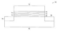
- FIG. 3illustrates a single transistor in an embodiment of a method to form a dielectric layer containing an ALD deposited hafnium nitride and hafnium oxide dielectric layer.
- a substrate 302is prepared, typically a silicon or silicon-containing material. In other embodiments, germanium, gallium arsenide, silicon-on-sapphire substrates, or other suitable substrates may also be used.
- the preparation processincludes cleaning substrate 302 and forming various layers and regions of the substrate, such as drain diffusion 304 and source diffusion 306 of an illustrative metal oxide semiconductor (MOS) transistor 300 , prior to forming a gate dielectric.
- MOSmetal oxide semiconductor
- the substrateis cleaned to provide an initial substrate depleted of its native oxide.
- the initial substrateis cleaned to provide a hydrogen-terminated surface.
- a silicon substrateundergoes a final hydrofluoric (HF) rinse prior to ALD processing to provide the silicon substrate with a hydrogen-terminated surface without a native silicon oxide layer. Cleaning immediately preceding atomic layer deposition aids in reducing an occurrence of silicon oxide at an interface between silicon based substrate and dielectric formed using the atomic layer deposition process.
- the sequencing of the formation of the regions of the transistor being processedmay follow the generally understood fabrication of a MOS transistor as is well known to those skilled in the art.
- the dielectric covering the area on the substrate 302 between the source and drain diffused regions 304 and 306may be deposited by ALD in this illustrative embodiment, and may comprise one or more hafnium oxide layers 310 and 314 , each potentially formed of many individual hafnium oxide layers, in an illustrative example, nine layers. There are also shown interleaved hafnium nitride layers 308 , 312 and 316 . Alternatively, there may be other combinations of interleaved and non-interleaved layers of varying thickness and deposition method. This nanolaminate dielectric layer is referred to as the gate oxide, and while shown as distinct and individual layers for clarity, may also be a single alloyed layer.
- the illustrative embodimentshows the hafnium oxide layers 310 and 314 having the same thickness; however, the desired dielectric properties of the overall dielectric film may be best achieved by adjusting the ratio of the thickness of the two dielectric layers to different values.
- the lowest dielectric in this illustrative exampleis a hafnium nitride layer, but the embodiments are not so limited, and hafnium oxide may be made the lowest layer.
- the transistor 300has a conductive material forming a gate 318 in this illustrative embodiment, but the dielectric may also be used in a floating gate device such as an EEPROM transistor, as either one or both of the floating gate and the control gate oxide layers.
- the conductive materialmay be polysilicon or various metals.
- the gate dielectric(layers 308 - 316 ) includes a tunnel gate insulator and a floating gate dielectric in a flash memory device.
- Use of dielectric layers containing an atomic layer deposited dielectric layer for a gate dielectric and/or floating gate dielectric in which the dielectric layer contacts a conductive layeris not limited to silicon based substrates, but may be used with a variety of semiconductor substrates.
- a methodincludes forming a first conductive layer 402 , a second conductive layer 404 , and having a dielectric having interleaved layers 406 - 416 of two or more different dielectric materials, such as hafnium oxide and hafnium nitride, formed between the two conductive layers.
- the conductive layers 402 and 404may include metals, doped polysilicon, silicided metals, polycides, or conductive organic compounds, without affecting the teachings of this embodiment.
- the sequencing and thickness of the individual dielectric layers 406 - 416depends on the application and may include a single layer of each material, one layer of one of the materials and multiple layers of the other, or other combinations of layers including different layer thicknesses.
- a nanolaminate structurecan be engineered to have a predetermined dielectric constant and composition.
- the total thickness of layers 408 , 412 and 416is equal to the thickness of layers 406 , 410 and 414 , providing a 50% combination of a first material (for example hafnium nitride) and a second material (for example hafnium oxide) and resulting in a dielectric layer having a dielectric constant k about halfway between the dielectric constant 17 of hafnium oxide and the dielectric constant 30 of hafnium nitride.
- the dielectric layersare shown in this illustrative example as being distinct layers, the oxide may be alloyed together to form a single material layer. Structures such as the nanolaminate structure shown in FIGS. 3 and 4 may be used in NROM flash memory devices as well as other integrated circuits. Transistors, capacitors, and other devices having dielectric films may be implemented into memory devices and electronic systems including information handling devices. Embodiments of these information handling devices include wireless systems, telecommunication systems, computers and integrated circuits.
- FIG. 5illustrates a diagram for an electronic system 500 having one or more devices having a dielectric layer containing an atomic layer deposited oxide layer formed according to various embodiments.
- Electronic system 500includes a controller 502 , a bus 504 , and an electronic device 506 , where bus 504 provides electrical conductivity between controller 502 and electronic device 506 .
- controller 502 and/or electronic device 506includes an embodiment for a dielectric layer containing an ALD deposited dielectric layer as previously discussed herein.
- Electronic system 500may include, but is not limited to, information handling devices, wireless systems, telecommunication systems, fiber optic systems, electro-optic systems, and computers.
- FIG. 6depicts a diagram of an embodiment of a system 600 having a controller 602 and a memory 606 .
- Controller 602 and/or memory 606includes a dielectric layer having an ALD dielectric layer.
- System 600also includes an electronic apparatus 608 , and a bus 604 , where bus 604 may provide electrical conductivity and data transmission between controller 602 and electronic apparatus 608 , and between controller 602 and memory 606 .
- Bus 604may include an address, a data bus, and a control bus, each independently configured.
- Bus 604also uses common conductive lines for providing address, data, and/or control, the use of which may be regulated by controller 602 .
- electronic apparatus 608includes additional memory devices configured similarly to memory 606 .
- An embodimentincludes an additional peripheral device or devices 610 coupled to bus 604 .
- controller 602is a processor. Any of controller 602 , memory 606 , bus 604 , electronic apparatus 608 , and peripheral device or devices 610 may include a dielectric layer having an ALD deposited oxide layer in accordance with the disclosed embodiments.
- System 600may include, but is not limited to, information handling devices, telecommunication systems, and computers.
- Peripheral devices 610may include displays, additional storage memory, or other control devices that may operate in conjunction with controller 602 and/or memory 606 . It will be understood that embodiments are equally applicable to any size and type of memory circuit and are not intended to be limited to a particular type of memory device.
- Memory typesinclude a DRAM, SRAM (Static Random Access Memory) or Flash memories. Additionally, the DRAM could be a synchronous DRAM commonly referred to as SGRAM (Synchronous Graphics Random Access Memory), SDRAM (Synchronous Dynamic Random Access Memory), SDRAM II, and DDR SDRAM (Double Data Rate SDRAM), as well as and other emerging DRAM technologies.
- Formation of hafnium oxide layers by ALD depositionmay be realized using a homoleptic tetrakisdialkylamine metal(IV) precursor chemical, and an oxidizing reactant, such as water vapor.
- Hafnium nitride layers by ALD depositionmay be realized by using a homoleptic tetrakisdialkylamine metal (IV) precursor chemical, and a reactant such as ammonia.
- such dielectric filmsmay be formed by ALD reactions processed at relatively low temperatures, such as 250° C., may be amorphous and possess smooth surfaces.
- Such ALD dielectric filmsmay provide enhanced electrical properties as compared to physical deposition methods, such as sputtering or typical chemical layer depositions, due to their smoother surface, and reduced damage, resulting in reduced leakage current. Additionally, such dielectric layers provide a significantly thicker physical thickness than a silicon oxide layer having the same electrical equivalent oxide thickness, where the increased thickness may also reduce leakage current issues. These properties of ALD deposited dielectric layers allow for application as dielectric layers in electronic devices and systems.
- Dielectric layers formed from hafnium nitride and hafnium oxidehave beneficial properties for gate dielectrics and capacitor dielectric materials including thermal stability, high dielectric constant and low leakage currents.
- the conductive layers contacting the dielectricmay include metals, semiconductor materials, polycrystalline semiconductor materials and doped materials of either conductivity type.
- Capacitors, transistors, higher level ICs or devices including memory devices, and electronic systemsare constructed utilizing the novel process for forming a dielectric film having an ultra thin equivalent oxide thickness, t eq .
- Gate dielectric layers or films containing atomic layer deposited hafnium oxideare formed having a dielectric constant (k) substantially higher than that of silicon oxide, such that these dielectric films possess an equivalent thickness, t eq , thinner than SiO 2 gate dielectrics of the same physical thickness.
- the high dielectric constant relative to silicon dioxideallows the use of much larger physical thickness of these high-k dielectric materials for the same t eq of SiO 2 . Films having the relatively larger physical thickness aids in processing gate dielectrics and other dielectric layers in electronic devices and systems, and improves the electrical properties of the dielectrics.
Landscapes
- Chemical & Material Sciences (AREA)
- Engineering & Computer Science (AREA)
- Chemical Kinetics & Catalysis (AREA)
- General Chemical & Material Sciences (AREA)
- Organic Chemistry (AREA)
- Metallurgy (AREA)
- Mechanical Engineering (AREA)
- Materials Engineering (AREA)
- General Physics & Mathematics (AREA)
- Power Engineering (AREA)
- Microelectronics & Electronic Packaging (AREA)
- Computer Hardware Design (AREA)
- Manufacturing & Machinery (AREA)
- Condensed Matter Physics & Semiconductors (AREA)
- Physics & Mathematics (AREA)
- Crystallography & Structural Chemistry (AREA)
- Inorganic Chemistry (AREA)
- Formation Of Insulating Films (AREA)
- Semiconductor Memories (AREA)
- Insulated Gate Type Field-Effect Transistor (AREA)
Abstract
Description
t=(k/kox)teq=(k/3.9) teq.
Thus, materials with a dielectric constant greater than that of SiO2will have a physical thickness that can be considerably larger than a desired teq, while providing the desired equivalent oxide thickness. For example, an alternate dielectric material with a dielectric constant of 10 could have a thickness of about 25.6 Å to provide a teqof 10 Å, not including any depletion/inversion layer effects. Thus, a reduced equivalent oxide thickness for transistors can be realized by using dielectric materials with higher dielectric constants than SiO2.
teq=tSiO2+(kox/k)t.
Thus, if a SiO2layer is formed in the process, the teqis again limited by a SiO2layer. In the event that a barrier layer is formed between the silicon layer and the desired dielectric in which the barrier layer prevents the formation of a SiO2layer, the teqwould be limited by the layer with the lowest dielectric constant. However, whether a single dielectric layer with a high dielectric constant or a barrier layer with a higher dielectric constant than SiO2is employed, the layer directly in contact, or interfacing with the silicon layer must provide a high quality interface to maintain high channel carrier mobility.
Claims (25)
Priority Applications (1)
| Application Number | Priority Date | Filing Date | Title |
|---|---|---|---|
| US12/359,748US7960803B2 (en) | 2005-02-23 | 2009-01-26 | Electronic device having a hafnium nitride and hafnium oxide film |
Applications Claiming Priority (2)
| Application Number | Priority Date | Filing Date | Title |
|---|---|---|---|
| US11/063,717US7498247B2 (en) | 2005-02-23 | 2005-02-23 | Atomic layer deposition of Hf3N4/HfO2 films as gate dielectrics |
| US12/359,748US7960803B2 (en) | 2005-02-23 | 2009-01-26 | Electronic device having a hafnium nitride and hafnium oxide film |
Related Parent Applications (1)
| Application Number | Title | Priority Date | Filing Date |
|---|---|---|---|
| US11/063,717ContinuationUS7498247B2 (en) | 2005-02-23 | 2005-02-23 | Atomic layer deposition of Hf3N4/HfO2 films as gate dielectrics |
Publications (2)
| Publication Number | Publication Date |
|---|---|
| US20090134499A1 US20090134499A1 (en) | 2009-05-28 |
| US7960803B2true US7960803B2 (en) | 2011-06-14 |
Family
ID=36913328
Family Applications (2)
| Application Number | Title | Priority Date | Filing Date |
|---|---|---|---|
| US11/063,717Active2025-11-07US7498247B2 (en) | 2005-02-23 | 2005-02-23 | Atomic layer deposition of Hf3N4/HfO2 films as gate dielectrics |
| US12/359,748Expired - LifetimeUS7960803B2 (en) | 2005-02-23 | 2009-01-26 | Electronic device having a hafnium nitride and hafnium oxide film |
Family Applications Before (1)
| Application Number | Title | Priority Date | Filing Date |
|---|---|---|---|
| US11/063,717Active2025-11-07US7498247B2 (en) | 2005-02-23 | 2005-02-23 | Atomic layer deposition of Hf3N4/HfO2 films as gate dielectrics |
Country Status (1)
| Country | Link |
|---|---|
| US (2) | US7498247B2 (en) |
Cited By (1)
| Publication number | Priority date | Publication date | Assignee | Title |
|---|---|---|---|---|
| US11251189B2 (en) | 2009-02-09 | 2022-02-15 | Longitude Flash Memory Solutions Ltd. | Gate fringing effect based channel formation for semiconductor device |
Families Citing this family (92)
| Publication number | Priority date | Publication date | Assignee | Title |
|---|---|---|---|---|
| US6852167B2 (en) | 2001-03-01 | 2005-02-08 | Micron Technology, Inc. | Methods, systems, and apparatus for uniform chemical-vapor depositions |
| US7068544B2 (en) | 2001-08-30 | 2006-06-27 | Micron Technology, Inc. | Flash memory with low tunnel barrier interpoly insulators |
| US8026161B2 (en) | 2001-08-30 | 2011-09-27 | Micron Technology, Inc. | Highly reliable amorphous high-K gate oxide ZrO2 |
| US7476925B2 (en) | 2001-08-30 | 2009-01-13 | Micron Technology, Inc. | Atomic layer deposition of metal oxide and/or low asymmetrical tunnel barrier interploy insulators |
| US7589029B2 (en) | 2002-05-02 | 2009-09-15 | Micron Technology, Inc. | Atomic layer deposition and conversion |
| US7160577B2 (en) | 2002-05-02 | 2007-01-09 | Micron Technology, Inc. | Methods for atomic-layer deposition of aluminum oxides in integrated circuits |
| US7135421B2 (en) | 2002-06-05 | 2006-11-14 | Micron Technology, Inc. | Atomic layer-deposited hafnium aluminum oxide |
| US6921702B2 (en) | 2002-07-30 | 2005-07-26 | Micron Technology Inc. | Atomic layer deposited nanolaminates of HfO2/ZrO2 films as gate dielectrics |
| US6884739B2 (en) | 2002-08-15 | 2005-04-26 | Micron Technology Inc. | Lanthanide doped TiOx dielectric films by plasma oxidation |
| US6790791B2 (en) | 2002-08-15 | 2004-09-14 | Micron Technology, Inc. | Lanthanide doped TiOx dielectric films |
| US7199023B2 (en) | 2002-08-28 | 2007-04-03 | Micron Technology, Inc. | Atomic layer deposited HfSiON dielectric films wherein each precursor is independendently pulsed |
| US7084078B2 (en) | 2002-08-29 | 2006-08-01 | Micron Technology, Inc. | Atomic layer deposited lanthanide doped TiOx dielectric films |
| US7101813B2 (en) | 2002-12-04 | 2006-09-05 | Micron Technology Inc. | Atomic layer deposited Zr-Sn-Ti-O films |
| US6958302B2 (en) | 2002-12-04 | 2005-10-25 | Micron Technology, Inc. | Atomic layer deposited Zr-Sn-Ti-O films using TiI4 |
| US7192892B2 (en) | 2003-03-04 | 2007-03-20 | Micron Technology, Inc. | Atomic layer deposited dielectric layers |
| US7135369B2 (en) | 2003-03-31 | 2006-11-14 | Micron Technology, Inc. | Atomic layer deposited ZrAlxOy dielectric layers including Zr4AlO9 |
| US7192824B2 (en) | 2003-06-24 | 2007-03-20 | Micron Technology, Inc. | Lanthanide oxide / hafnium oxide dielectric layers |
| US7601649B2 (en) | 2004-08-02 | 2009-10-13 | Micron Technology, Inc. | Zirconium-doped tantalum oxide films |
| US7081421B2 (en) | 2004-08-26 | 2006-07-25 | Micron Technology, Inc. | Lanthanide oxide dielectric layer |
| US7494939B2 (en) | 2004-08-31 | 2009-02-24 | Micron Technology, Inc. | Methods for forming a lanthanum-metal oxide dielectric layer |
| US7588988B2 (en) | 2004-08-31 | 2009-09-15 | Micron Technology, Inc. | Method of forming apparatus having oxide films formed using atomic layer deposition |
| US7235501B2 (en) | 2004-12-13 | 2007-06-26 | Micron Technology, Inc. | Lanthanum hafnium oxide dielectrics |
| US7560395B2 (en) | 2005-01-05 | 2009-07-14 | Micron Technology, Inc. | Atomic layer deposited hafnium tantalum oxide dielectrics |
| US7508648B2 (en)* | 2005-02-08 | 2009-03-24 | Micron Technology, Inc. | Atomic layer deposition of Dy doped HfO2 films as gate dielectrics |
| US7374964B2 (en) | 2005-02-10 | 2008-05-20 | Micron Technology, Inc. | Atomic layer deposition of CeO2/Al2O3 films as gate dielectrics |
| US7399666B2 (en)* | 2005-02-15 | 2008-07-15 | Micron Technology, Inc. | Atomic layer deposition of Zr3N4/ZrO2 films as gate dielectrics |
| US7498247B2 (en)* | 2005-02-23 | 2009-03-03 | Micron Technology, Inc. | Atomic layer deposition of Hf3N4/HfO2 films as gate dielectrics |
| KR100584783B1 (en)* | 2005-02-24 | 2006-05-30 | 삼성전자주식회사 | Composite film formation method and gate structure and capacitor manufacturing method using the same |
| US7365027B2 (en) | 2005-03-29 | 2008-04-29 | Micron Technology, Inc. | ALD of amorphous lanthanide doped TiOx films |
| US7687409B2 (en) | 2005-03-29 | 2010-03-30 | Micron Technology, Inc. | Atomic layer deposited titanium silicon oxide films |
| US7390756B2 (en) | 2005-04-28 | 2008-06-24 | Micron Technology, Inc. | Atomic layer deposited zirconium silicon oxide films |
| US7662729B2 (en) | 2005-04-28 | 2010-02-16 | Micron Technology, Inc. | Atomic layer deposition of a ruthenium layer to a lanthanide oxide dielectric layer |
| US20060267113A1 (en)* | 2005-05-27 | 2006-11-30 | Tobin Philip J | Semiconductor device structure and method therefor |
| US7572695B2 (en) | 2005-05-27 | 2009-08-11 | Micron Technology, Inc. | Hafnium titanium oxide films |
| JP2006344837A (en)* | 2005-06-09 | 2006-12-21 | Matsushita Electric Ind Co Ltd | Semiconductor device and manufacturing method thereof |
| US7432139B2 (en) | 2005-06-29 | 2008-10-07 | Amberwave Systems Corp. | Methods for forming dielectrics and metal electrodes |
| US20070001231A1 (en)* | 2005-06-29 | 2007-01-04 | Amberwave Systems Corporation | Material systems for dielectrics and metal electrodes |
| US7927948B2 (en) | 2005-07-20 | 2011-04-19 | Micron Technology, Inc. | Devices with nanocrystals and methods of formation |
| US7575978B2 (en) | 2005-08-04 | 2009-08-18 | Micron Technology, Inc. | Method for making conductive nanoparticle charge storage element |
| US7989290B2 (en) | 2005-08-04 | 2011-08-02 | Micron Technology, Inc. | Methods for forming rhodium-based charge traps and apparatus including rhodium-based charge traps |
| US7402534B2 (en)* | 2005-08-26 | 2008-07-22 | Applied Materials, Inc. | Pretreatment processes within a batch ALD reactor |
| US8110469B2 (en) | 2005-08-30 | 2012-02-07 | Micron Technology, Inc. | Graded dielectric layers |
| US7410910B2 (en) | 2005-08-31 | 2008-08-12 | Micron Technology, Inc. | Lanthanum aluminum oxynitride dielectric films |
| US7972974B2 (en) | 2006-01-10 | 2011-07-05 | Micron Technology, Inc. | Gallium lanthanide oxide films |
| US7709402B2 (en) | 2006-02-16 | 2010-05-04 | Micron Technology, Inc. | Conductive layers for hafnium silicon oxynitride films |
| US7816737B2 (en)* | 2006-03-31 | 2010-10-19 | Tokyo Electron Limited | Semiconductor device with gate dielectric containing mixed rare earth elements |
| US8012442B2 (en)* | 2006-03-31 | 2011-09-06 | Tokyo Electron Limited | Method of forming mixed rare earth nitride and aluminum nitride films by atomic layer deposition |
| US7759746B2 (en)* | 2006-03-31 | 2010-07-20 | Tokyo Electron Limited | Semiconductor device with gate dielectric containing aluminum and mixed rare earth elements |
| US20070237697A1 (en)* | 2006-03-31 | 2007-10-11 | Tokyo Electron Limited | Method of forming mixed rare earth oxide and aluminate films by atomic layer deposition |
| US8097300B2 (en)* | 2006-03-31 | 2012-01-17 | Tokyo Electron Limited | Method of forming mixed rare earth oxynitride and aluminum oxynitride films by atomic layer deposition |
| US7582161B2 (en) | 2006-04-07 | 2009-09-01 | Micron Technology, Inc. | Atomic layer deposited titanium-doped indium oxide films |
| US7727908B2 (en) | 2006-08-03 | 2010-06-01 | Micron Technology, Inc. | Deposition of ZrA1ON films |
| US7582549B2 (en) | 2006-08-25 | 2009-09-01 | Micron Technology, Inc. | Atomic layer deposited barium strontium titanium oxide films |
| US7432548B2 (en) | 2006-08-31 | 2008-10-07 | Micron Technology, Inc. | Silicon lanthanide oxynitride films |
| US7759747B2 (en) | 2006-08-31 | 2010-07-20 | Micron Technology, Inc. | Tantalum aluminum oxynitride high-κ dielectric |
| US7544604B2 (en) | 2006-08-31 | 2009-06-09 | Micron Technology, Inc. | Tantalum lanthanide oxynitride films |
| US7605030B2 (en) | 2006-08-31 | 2009-10-20 | Micron Technology, Inc. | Hafnium tantalum oxynitride high-k dielectric and metal gates |
| US7563730B2 (en) | 2006-08-31 | 2009-07-21 | Micron Technology, Inc. | Hafnium lanthanide oxynitride films |
| US7776765B2 (en) | 2006-08-31 | 2010-08-17 | Micron Technology, Inc. | Tantalum silicon oxynitride high-k dielectrics and metal gates |
| US7767262B2 (en)* | 2006-09-29 | 2010-08-03 | Tokyo Electron Limited | Nitrogen profile engineering in nitrided high dielectric constant films |
| US20080079111A1 (en)* | 2006-09-29 | 2008-04-03 | Tokyo Electron Limited | Semiconductor devices containing nitrided high dielectric constant films |
| US8067772B2 (en)* | 2006-12-05 | 2011-11-29 | Semiconductor Energy Laboratory Co., Ltd. | Semiconductor device and manufacturing method thereof |
| US8367506B2 (en) | 2007-06-04 | 2013-02-05 | Micron Technology, Inc. | High-k dielectrics with gold nano-particles |
| US7632745B2 (en)* | 2007-06-30 | 2009-12-15 | Intel Corporation | Hybrid high-k gate dielectric film |
| US7772073B2 (en)* | 2007-09-28 | 2010-08-10 | Tokyo Electron Limited | Semiconductor device containing a buried threshold voltage adjustment layer and method of forming |
| FR2928663A1 (en)* | 2008-03-17 | 2009-09-18 | Centre Nat Rech Scient | PROCESS FOR PRODUCING A THIN FILM OF OXIDE OR HAFNIUM SILICATE NITRIDE, COORDINATION COMPOUND USED IN THIS METHOD AND METHOD FOR PRODUCING AN INTEGRATED ELECTRONIC CIRCUIT |
| US8679962B2 (en) | 2008-08-21 | 2014-03-25 | Taiwan Semiconductor Manufacturing Company, Ltd. | Integrated circuit metal gate structure and method of fabrication |
| US8076241B2 (en)* | 2009-09-30 | 2011-12-13 | Tokyo Electron Limited | Methods for multi-step copper plating on a continuous ruthenium film in recessed features |
| JP5963456B2 (en)* | 2011-02-18 | 2016-08-03 | 株式会社日立国際電気 | Semiconductor device manufacturing method, substrate processing apparatus, and substrate processing method |
| US8847196B2 (en)* | 2011-05-17 | 2014-09-30 | Micron Technology, Inc. | Resistive memory cell |
| US8846443B2 (en)* | 2011-08-05 | 2014-09-30 | Intermolecular, Inc. | Atomic layer deposition of metal oxides for memory applications |
| US8440520B2 (en) | 2011-08-23 | 2013-05-14 | Tokyo Electron Limited | Diffused cap layers for modifying high-k gate dielectrics and interface layers |
| JP2013077805A (en)* | 2011-09-16 | 2013-04-25 | Hitachi Kokusai Electric Inc | Method of manufacturing semiconductor device, substrate processing method, substrate processing apparatus, and program |
| US9318336B2 (en) | 2011-10-27 | 2016-04-19 | Globalfoundries U.S. 2 Llc | Non-volatile memory structure employing high-k gate dielectric and metal gate |
| US8633118B2 (en) | 2012-02-01 | 2014-01-21 | Tokyo Electron Limited | Method of forming thin metal and semi-metal layers by thermal remote oxygen scavenging |
| US8865538B2 (en) | 2012-03-30 | 2014-10-21 | Tokyo Electron Limited | Method of integrating buried threshold voltage adjustment layers for CMOS processing |
| US20130316546A1 (en)* | 2012-05-24 | 2013-11-28 | Intermolecular, Inc. | Methods of atomic layer deposition of hafnium oxide as gate dielectrics |
| US8865581B2 (en) | 2012-10-19 | 2014-10-21 | Tokyo Electron Limited | Hybrid gate last integration scheme for multi-layer high-k gate stacks |
| KR102106259B1 (en) | 2013-08-16 | 2020-05-04 | 삼성전자 주식회사 | Method for forming a trench of semiconductor device |
| TWI590329B (en)* | 2014-03-02 | 2017-07-01 | 東京威力科創股份有限公司 | Method for improving nucleation rate and electrical mobility of high dielectric constant film in semiconductor device by microwave plasma treatment |
| KR102230196B1 (en) | 2015-04-23 | 2021-03-19 | 삼성전자주식회사 | Semiconductor device and method for manufacturing the same |
| CN110024089B (en)* | 2016-11-30 | 2023-06-27 | 株式会社理光 | Oxide or oxynitride insulator film and coating solution for forming same, field effect transistor and manufacturing method thereof |
| US10816891B2 (en) | 2016-12-14 | 2020-10-27 | Taiwan Semiconductor Manufacturing Company, Ltd. | Photomask and fabrication method therefor |
| US11923404B2 (en) | 2018-04-02 | 2024-03-05 | Lam Research Corporation | Modifying ferroelectric properties of hafnium oxide with hafnium nitride layers |
| US12256547B2 (en) | 2020-01-22 | 2025-03-18 | Sunrise Memory Corporation | Silicon oxide nitride tunnel dielectric for a storage transistor in a 3-dimensional NOR memory string array |
| TWI767512B (en)* | 2020-01-22 | 2022-06-11 | 美商森恩萊斯記憶體公司 | Cool electron erasing in thin-film storage transistors |
| CN111883543B (en)* | 2020-07-28 | 2022-09-27 | 北海惠科光电技术有限公司 | Manufacturing method of array substrate, array substrate and display device |
| CN112349792B (en)* | 2020-11-06 | 2023-01-31 | 浙江师范大学 | Monocrystalline silicon passivation contact structure and preparation method thereof |
| CN114985551B (en)* | 2022-05-31 | 2023-10-31 | 宜兴市联丰化工机械有限公司 | Warm-pressing forming process of stainless steel seal head |
| CN115274420B (en)* | 2022-08-15 | 2024-07-26 | 福州大学 | Preparation method of ALD hafnium dioxide thin film based on flexible substrate |
| CN116960166B (en)* | 2023-09-14 | 2023-11-24 | 泉州师范学院 | A high dielectric constant nano-laminated dielectric film and its preparation method |
| CN119230414A (en)* | 2024-12-04 | 2024-12-31 | 苏州烯晶半导体科技有限公司 | A preparation process for a gate dielectric layer on the surface of a low-dimensional material field effect transistor |
Citations (131)
| Publication number | Priority date | Publication date | Assignee | Title |
|---|---|---|---|---|
| US3357961A (en) | 1965-05-24 | 1967-12-12 | Exxon Research Engineering Co | Copolymers of ethylene and hexadiene 1, 5 |
| US4215156A (en) | 1977-08-26 | 1980-07-29 | International Business Machines Corporation | Method for fabricating tantalum semiconductor contacts |
| EP0540993A1 (en) | 1991-11-06 | 1993-05-12 | Ramtron International Corporation | Structure and fabrication of high transconductance MOS field effect transistor using a buffer layer/ferroelectric/buffer layer stack as the gate dielectric |
| US5562952A (en) | 1993-11-11 | 1996-10-08 | Nissin Electric Co., Ltd. | Plasma-CVD method and apparatus |
| US5572052A (en) | 1992-07-24 | 1996-11-05 | Mitsubishi Denki Kabushiki Kaisha | Electronic device using zirconate titanate and barium titanate ferroelectrics in insulating layer |
| US5674563A (en) | 1993-09-14 | 1997-10-07 | Nissan Motor Co., Ltd. | Method for ferroelectric thin film production |
| US5698022A (en) | 1996-08-14 | 1997-12-16 | Advanced Technology Materials, Inc. | Lanthanide/phosphorus precursor compositions for MOCVD of lanthanide/phosphorus oxide films |
| US5745334A (en) | 1996-03-25 | 1998-04-28 | International Business Machines Corporation | Capacitor formed within printed circuit board |
| US5751021A (en) | 1995-04-24 | 1998-05-12 | Sharp Kk | Semiconductor light-emitting device |
| US5795808A (en) | 1995-11-13 | 1998-08-18 | Hyundai Electronics Industries C., Ltd. | Method for forming shallow junction for semiconductor device |
| US5827571A (en) | 1994-06-08 | 1998-10-27 | Hyundai Electronics Industries Co., Ltd. | Hot-wall CVD method for forming a ferroelectric film |
| US6013553A (en) | 1997-07-24 | 2000-01-11 | Texas Instruments Incorporated | Zirconium and/or hafnium oxynitride gate dielectric |
| US6203613B1 (en) | 1999-10-19 | 2001-03-20 | International Business Machines Corporation | Atomic layer deposition with nitrate containing precursors |
| US6225168B1 (en) | 1998-06-04 | 2001-05-01 | Advanced Micro Devices, Inc. | Semiconductor device having metal gate electrode and titanium or tantalum nitride gate dielectric barrier layer and process of fabrication thereof |
| EP1096042A1 (en) | 1999-10-25 | 2001-05-02 | Motorola, Inc. | Method for fabricating a semiconductor structure including a metal oxide interface with silicon |
| US6297539B1 (en) | 1999-07-19 | 2001-10-02 | Sharp Laboratories Of America, Inc. | Doped zirconia, or zirconia-like, dielectric film transistor structure and deposition method for same |
| US6303481B2 (en) | 1999-12-29 | 2001-10-16 | Hyundai Electronics Industries Co., Ltd. | Method for forming a gate insulating film for semiconductor devices |
| US20010030352A1 (en) | 2000-02-29 | 2001-10-18 | Alexander Ruf | Method for increasing the capacitance in a storage trench and trench capacitor having increased capacitance |
| US6348386B1 (en) | 2001-04-16 | 2002-02-19 | Motorola, Inc. | Method for making a hafnium-based insulating film |
| US20020037615A1 (en) | 2000-09-27 | 2002-03-28 | Kouji Matsuo | Semiconductor device and method of fabricating the same |
| US20020068466A1 (en) | 2000-12-06 | 2002-06-06 | Seung-Hwan Lee | Methods of forming thin films by atomic layer deposition |
| US20020089023A1 (en) | 2001-01-05 | 2002-07-11 | Motorola, Inc. | Low leakage current metal oxide-nitrides and method of fabricating same |
| US6420279B1 (en) | 2001-06-28 | 2002-07-16 | Sharp Laboratories Of America, Inc. | Methods of using atomic layer deposition to deposit a high dielectric constant material on a substrate |
| US20020094632A1 (en) | 2000-08-31 | 2002-07-18 | Agarwal Vishnu K. | Capacitor fabrication methods and capacitor constructions |
| US20020111001A1 (en) | 2001-02-09 | 2002-08-15 | Micron Technology, Inc. | Formation of metal oxide gate dielectric |
| US6436799B1 (en) | 2000-09-26 | 2002-08-20 | Cypress Semiconductor, Corporation | Process for annealing semiconductors and/or integrated circuits |
| US6451695B2 (en) | 1999-03-11 | 2002-09-17 | Genus, Inc. | Radical-assisted sequential CVD |
| US6452229B1 (en) | 2002-02-21 | 2002-09-17 | Advanced Micro Devices, Inc. | Ultra-thin fully depleted SOI device with T-shaped gate and method of fabrication |
| US20020146916A1 (en) | 2001-03-29 | 2002-10-10 | Kiyoshi Irino | Semiconductor device having a high-dielectric gate insulation film and fabrication process thereof |
| US20020155688A1 (en) | 2001-04-20 | 2002-10-24 | Ahn Kie Y. | Highly reliable gate oxide and method of fabrication |
| US20020172768A1 (en) | 2001-05-21 | 2002-11-21 | Nec Corporation | Method for vapor deposition of a metal compound film |
| US20020177293A1 (en) | 1999-02-26 | 2002-11-28 | Wilk Glen D. | Hafnium nitride gate dielectric |
| US20020192975A1 (en) | 2001-06-13 | 2002-12-19 | Ahn Kie Y. | Dielectric layer forming method and devices formed therewith |
| US6498065B1 (en) | 1998-08-04 | 2002-12-24 | Micron Technology, Inc. | Memory address decode array with vertical transistors |
| US6509280B2 (en) | 2001-02-22 | 2003-01-21 | Samsung Electronics Co., Ltd. | Method for forming a dielectric layer of a semiconductor device |
| US20030017717A1 (en) | 2001-07-18 | 2003-01-23 | Ahn Kie Y. | Methods for forming dielectric materials and methods for forming semiconductor devices |
| US6518634B1 (en) | 2000-09-01 | 2003-02-11 | Motorola, Inc. | Strontium nitride or strontium oxynitride gate dielectric |
| US20030045078A1 (en) | 2001-08-30 | 2003-03-06 | Micron Technology, Inc. | Highly reliable amorphous high-K gate oxide ZrO2 |
| US20030043637A1 (en) | 2001-08-30 | 2003-03-06 | Micron Technology, Inc | Flash memory with low tunnel barrier interpoly insulators |
| US20030045060A1 (en) | 2001-08-30 | 2003-03-06 | Micron Technology, Inc. | Crystalline or amorphous medium-k gate oxides, Y2O3 and Gd2O3 |
| US20030049942A1 (en) | 2001-08-31 | 2003-03-13 | Suvi Haukka | Low temperature gate stack |
| US20030048666A1 (en) | 2001-08-30 | 2003-03-13 | Micron Technology, Inc. | Graded composition metal oxide tunnel barrier interpoly insulators |
| US20030059535A1 (en) | 2001-09-25 | 2003-03-27 | Lee Luo | Cycling deposition of low temperature films in a cold wall single wafer process chamber |
| US6541079B1 (en) | 1999-10-25 | 2003-04-01 | International Business Machines Corporation | Engineered high dielectric constant oxide and oxynitride heterostructure gate dielectrics by an atomic beam deposition technique |
| US6551929B1 (en) | 2000-06-28 | 2003-04-22 | Applied Materials, Inc. | Bifurcated deposition process for depositing refractory metal layers employing atomic layer deposition and chemical vapor deposition techniques |
| US6559014B1 (en) | 2001-10-15 | 2003-05-06 | Advanced Micro Devices, Inc. | Preparation of composite high-K / standard-K dielectrics for semiconductor devices |
| US6559007B1 (en) | 2000-04-06 | 2003-05-06 | Micron Technology, Inc. | Method for forming flash memory device having a tunnel dielectric comprising nitrided oxide |
| US6562491B1 (en) | 2001-10-15 | 2003-05-13 | Advanced Micro Devices, Inc. | Preparation of composite high-K dielectrics |
| US20030104666A1 (en) | 2001-02-05 | 2003-06-05 | International Business Machines Corporation | Method for forming dielectric stack without interfacial layer |
| US20030119291A1 (en) | 2001-12-20 | 2003-06-26 | Micron Technology, Inc. | Low-temperature grown high-quality ultra-thin praseodymium gate dielectrics |
| US20030116804A1 (en) | 2001-12-26 | 2003-06-26 | Visokay Mark Robert | Bilayer deposition to avoid unwanted interfacial reactions during high K gate dielectric processing |
| US20030119246A1 (en) | 2001-12-20 | 2003-06-26 | Micron Technology, Inc. | Low-temperature grown high quality ultra-thin CoTiO3 gate dielectrics |
| US6590252B2 (en) | 2000-11-06 | 2003-07-08 | Matsushita Electric Industrial Co., Ltd. | Semiconductor device with oxygen diffusion barrier layer termed from composite nitride |
| US6592942B1 (en) | 2000-07-07 | 2003-07-15 | Asm International N.V. | Method for vapour deposition of a film onto a substrate |
| US20030132491A1 (en) | 2002-01-17 | 2003-07-17 | Micron Technology, Inc. | Highly reliable amorphous high-K gate dielectric ZrOxNy |
| US6617639B1 (en) | 2002-06-21 | 2003-09-09 | Advanced Micro Devices, Inc. | Use of high-K dielectric material for ONO and tunnel oxide to improve floating gate flash memory coupling |
| US20030176049A1 (en) | 2002-03-15 | 2003-09-18 | Hegde Rama I. | Gate dielectric and method therefor |
| US20030185980A1 (en) | 2002-04-01 | 2003-10-02 | Nec Corporation | Thin film forming method and a semiconductor device manufacturing method |
| US6632279B1 (en) | 1999-10-14 | 2003-10-14 | Asm Microchemistry, Oy | Method for growing thin oxide films |
| US6638859B2 (en) | 1999-12-22 | 2003-10-28 | Genus, Inc. | Apparatus and method to achieve continuous interface and ultrathin film during atomic layer deposition |
| US20030207540A1 (en) | 2002-05-02 | 2003-11-06 | Micron Technology, Inc. | Atomic layer-deposited laaio3 films for gate dielectrics |
| US20030207032A1 (en) | 2002-05-02 | 2003-11-06 | Micron Technology, Inc. | Methods, systems, and apparatus for atomic-layer deposition of aluminum oxides in integrated circuits |
| US6652924B2 (en) | 1996-08-16 | 2003-11-25 | Licensee For Microelectronics: Asm America, Inc. | Sequential chemical vapor deposition |
| US6656764B1 (en) | 2002-05-15 | 2003-12-02 | Taiwan Semiconductor Manufacturing Company | Process for integration of a high dielectric constant gate insulator layer in a CMOS device |
| US20030227033A1 (en) | 2002-06-05 | 2003-12-11 | Micron Technology, Inc. | Atomic layer-deposited HfA1O3 films for gate dielectrics |
| US20030232501A1 (en) | 2002-06-14 | 2003-12-18 | Kher Shreyas S. | Surface pre-treatment for enhancement of nucleation of high dielectric constant materials |
| US20030232511A1 (en) | 2002-06-14 | 2003-12-18 | Applied Materials, Inc. | ALD metal oxide deposition process using direct oxidation |
| US20030235961A1 (en) | 2002-04-17 | 2003-12-25 | Applied Materials, Inc. | Cyclical sequential deposition of multicomponent films |
| US6674138B1 (en) | 2001-12-31 | 2004-01-06 | Advanced Micro Devices, Inc. | Use of high-k dielectric materials in modified ONO structure for semiconductor devices |
| US20040009679A1 (en) | 2001-01-19 | 2004-01-15 | Yeo Jae-Hyun | Method of forming material using atomic layer deposition and method of forming capacitor of semiconductor device using the same |
| US20040012043A1 (en) | 2002-07-17 | 2004-01-22 | Gealy F. Daniel | Novel dielectric stack and method of making same |
| US6686212B1 (en) | 2002-10-31 | 2004-02-03 | Sharp Laboratories Of America, Inc. | Method to deposit a stacked high-κ gate dielectric for CMOS applications |
| US20040023461A1 (en) | 2002-07-30 | 2004-02-05 | Micron Technology, Inc. | Atomic layer deposited nanolaminates of HfO2/ZrO2 films as gate dielectrics |
| US20040028811A1 (en) | 2002-08-06 | 2004-02-12 | Young-Jin Cho | Bismuth titanium silicon oxide, bismuth titanium silicon oxide thin film, and method for forming the thin film |
| US20040033661A1 (en) | 2002-08-16 | 2004-02-19 | Yeo Jae-Hyun | Semiconductor device and method for manufacturing the same |
| US20040038554A1 (en) | 2002-08-21 | 2004-02-26 | Ahn Kie Y. | Composite dielectric forming methods and composite dielectrics |
| US20040043541A1 (en) | 2002-08-29 | 2004-03-04 | Ahn Kie Y. | Atomic layer deposited lanthanide doped TiOx dielectric films |
| US20040043635A1 (en) | 2002-08-28 | 2004-03-04 | Micron Technology, Inc. | Systems and methods for forming metal oxides using metal diketonates and/or ketoimines |
| US20040043569A1 (en) | 2002-08-28 | 2004-03-04 | Ahn Kie Y. | Atomic layer deposited HfSiON dielectric films |
| US6709989B2 (en) | 2001-06-21 | 2004-03-23 | Motorola, Inc. | Method for fabricating a semiconductor structure including a metal oxide interface with silicon |
| US20040110348A1 (en) | 2002-12-04 | 2004-06-10 | Micron Technology, Inc. | Atomic layer deposited Zr-Sn-Ti-O films using TiI4 |
| US20040110391A1 (en) | 2002-12-04 | 2004-06-10 | Micron Technology, Inc. | Atomic layer deposited Zr-Sn-Ti-O films |
| US6750126B1 (en) | 2003-01-08 | 2004-06-15 | Texas Instruments Incorporated | Methods for sputter deposition of high-k dielectric films |
| US6756298B2 (en) | 2000-01-18 | 2004-06-29 | Micron Technology, Inc. | Methods and apparatus for making integrated-circuit wiring from copper, silver, gold, and other metals |
| US20040135186A1 (en) | 2002-12-27 | 2004-07-15 | Nec Electronics Corporation | Semiconductor device and method for manufacturing same |
| US20040144980A1 (en) | 2003-01-27 | 2004-07-29 | Ahn Kie Y. | Atomic layer deposition of metal oxynitride layers as gate dielectrics and semiconductor device structures utilizing metal oxynitride layers |
| US6770536B2 (en) | 2002-10-03 | 2004-08-03 | Agere Systems Inc. | Process for semiconductor device fabrication in which a insulating layer is formed on a semiconductor substrate |
| US6777353B2 (en) | 2000-04-14 | 2004-08-17 | Asm Microchemistry Oy | Process for producing oxide thin films |
| US6780704B1 (en) | 1999-12-03 | 2004-08-24 | Asm International Nv | Conformal thin films over textured capacitor electrodes |
| US20040171280A1 (en) | 2003-02-27 | 2004-09-02 | Sharp Laboratories Of America, Inc. | Atomic layer deposition of nanolaminate film |
| US20040168627A1 (en) | 2003-02-27 | 2004-09-02 | Sharp Laboratories Of America, Inc. | Atomic layer deposition of oxide film |
| US20040175882A1 (en) | 2003-03-04 | 2004-09-09 | Micron Technology, Inc. | Atomic layer deposited dielectric layers |
| US6790791B2 (en) | 2002-08-15 | 2004-09-14 | Micron Technology, Inc. | Lanthanide doped TiOx dielectric films |
| US6794315B1 (en) | 2003-03-06 | 2004-09-21 | Board Of Trustees Of The University Of Illinois | Ultrathin oxide films on semiconductors |
| US6800567B2 (en) | 2001-08-27 | 2004-10-05 | Hynix Semiconductor Inc. | Method for forming polyatomic layers |
| US6803311B2 (en) | 2002-09-17 | 2004-10-12 | Hynix Semiconductor Inc. | Method for forming metal films |
| US20040203254A1 (en) | 2003-04-11 | 2004-10-14 | Sharp Laboratories Of America, Inc. | Modulated temperature method of atomic layer deposition (ALD) of high dielectric constant films |
| US6808978B2 (en) | 2002-04-26 | 2004-10-26 | Hynix Semiconductor Inc. | Method for fabricating metal electrode with atomic layer deposition (ALD) in semiconductor device |
| US20040214399A1 (en) | 2003-04-22 | 2004-10-28 | Micron Technology, Inc. | Atomic layer deposited ZrTiO4 films |
| US6812100B2 (en) | 2002-03-13 | 2004-11-02 | Micron Technology, Inc. | Evaporation of Y-Si-O films for medium-k dielectrics |
| US6821873B2 (en) | 2002-01-10 | 2004-11-23 | Texas Instruments Incorporated | Anneal sequence for high-κ film property optimization |
| US6821862B2 (en) | 2000-06-27 | 2004-11-23 | Samsung Electronics Co., Ltd. | Methods of manufacturing integrated circuit devices that include a metal oxide layer disposed on another layer to protect the other layer from diffusion of impurities and integrated circuit devices manufactured using same |
| US20040235313A1 (en) | 2002-11-27 | 2004-11-25 | Agere Systems, Inc. | Process for fabricating a semiconductor device having an insulating layer formed over a semiconductor substrate |
| US6828632B2 (en) | 2002-07-18 | 2004-12-07 | Micron Technology, Inc. | Stable PD-SOI devices and methods |
| US20040262700A1 (en) | 2003-06-24 | 2004-12-30 | Micron Technology, Inc. | Lanthanide oxide / hafnium oxide dielectrics |
| US20040266217A1 (en) | 2003-06-24 | 2004-12-30 | Kyoung-Seok Kim | Method of forming high dielectric film using atomic layer deposition and method of manufacturing capacitor having the high dielectric film |
| US6844260B2 (en) | 2003-01-30 | 2005-01-18 | Micron Technology, Inc. | Insitu post atomic layer deposition destruction of active species |
| US20050020017A1 (en) | 2003-06-24 | 2005-01-27 | Micron Technology, Inc. | Lanthanide oxide / hafnium oxide dielectric layers |
| US20050023594A1 (en) | 2002-06-05 | 2005-02-03 | Micron Technology, Inc. | Pr2O3-based la-oxide gate dielectrics |
| US20050026458A1 (en) | 2003-07-03 | 2005-02-03 | Cem Basceri | Methods of forming hafnium-containing materials, methods of forming hafnium oxide, and constructions comprising hafnium oxide |
| US20050054165A1 (en) | 2003-03-31 | 2005-03-10 | Micron Technology, Inc. | Atomic layer deposited ZrAlxOy dielectric layers |
| US20050051828A1 (en) | 2003-04-22 | 2005-03-10 | Park Ki-Yeon | Methods of forming metal thin films, lanthanum oxide films, and high dielectric films for semiconductor devices using atomic layer deposition |
| US20050077519A1 (en) | 2003-10-10 | 2005-04-14 | Kie Ahn | Lanthanide oxide/zirconium oxide atomic layer deposited nanolaminate gate dielectrics |
| US6888739B2 (en) | 2002-06-21 | 2005-05-03 | Micron Technology Inc. | Nanocrystal write once read only memory for archival storage |
| US6893984B2 (en) | 2002-02-20 | 2005-05-17 | Micron Technology Inc. | Evaporated LaA1O3 films for gate dielectrics |
| US20050205947A1 (en) | 2004-03-17 | 2005-09-22 | National University Of Singapore | Thermal robust semiconductor device using HfN as metal gate electrode and the manufacturing process thereof |
| US20050275033A1 (en) | 2004-05-11 | 2005-12-15 | Shiyang Zhu | Schottky barrier source/drain N-MOSFET using ytterbium silicide |
| US6989565B1 (en) | 2002-04-15 | 2006-01-24 | Lsi Logic Corporation | Memory device having an electron trapping layer in a high-K dielectric gate stack |
| US20060022283A1 (en) | 2004-07-30 | 2006-02-02 | Thomas Shawn G | Interfacial layer for use with high k dielectric materials |
| US20060054943A1 (en) | 2004-09-14 | 2006-03-16 | Infineon Technologies North America Corp. | Flash EEPROM with metal floating gate electrode |
| US20060183272A1 (en) | 2005-02-15 | 2006-08-17 | Micron Technology, Inc. | Atomic layer deposition of Zr3N4/ZrO2 films as gate dielectrics |
| US20060189164A1 (en) | 2003-03-07 | 2006-08-24 | Nikko Materials Co., Ltd | Hafnium alloy target and process for producing the same |
| US20060208215A1 (en) | 2003-04-04 | 2006-09-21 | Craig Metzner | Method for hafnium nitride deposition |
| US20070010061A1 (en) | 2005-07-07 | 2007-01-11 | Micron Technology, Inc. | Metal-substituted transistor gates |
| US20070018214A1 (en) | 2005-07-25 | 2007-01-25 | Micron Technology, Inc. | Magnesium titanium oxide films |
| US20070020835A1 (en) | 2005-02-10 | 2007-01-25 | Micron Technology, Inc. | Atomic layer deposition of CeO2/Al2O3 films as gate dielectrics |
| US20070037415A1 (en) | 2004-12-13 | 2007-02-15 | Micron Technology, Inc. | Lanthanum hafnium oxide dielectrics |
| US20070045752A1 (en) | 2005-08-31 | 2007-03-01 | Leonard Forbes | Self aligned metal gates on high-K dielectrics |
| US20070134931A1 (en) | 2005-12-08 | 2007-06-14 | Micron Technology, Inc. | Lanthanide yttrium aluminum oxide dielectric films |
| US7410910B2 (en) | 2005-08-31 | 2008-08-12 | Micron Technology, Inc. | Lanthanum aluminum oxynitride dielectric films |
| US7498247B2 (en) | 2005-02-23 | 2009-03-03 | Micron Technology, Inc. | Atomic layer deposition of Hf3N4/HfO2 films as gate dielectrics |
Family Cites Families (4)
| Publication number | Priority date | Publication date | Assignee | Title |
|---|---|---|---|---|
| US6407435B1 (en) | 2000-02-11 | 2002-06-18 | Sharp Laboratories Of America, Inc. | Multilayer dielectric stack and method |
| US6660660B2 (en) | 2000-10-10 | 2003-12-09 | Asm International, Nv. | Methods for making a dielectric stack in an integrated circuit |
| US6884739B2 (en)* | 2002-08-15 | 2005-04-26 | Micron Technology Inc. | Lanthanide doped TiOx dielectric films by plasma oxidation |
| KR100945648B1 (en)* | 2002-10-29 | 2010-03-04 | 매그나칩 반도체 유한회사 | Transistor of semiconductor device and manufacturing method thereof |
- 2005
- 2005-02-23USUS11/063,717patent/US7498247B2/enactiveActive
- 2009
- 2009-01-26USUS12/359,748patent/US7960803B2/ennot_activeExpired - Lifetime
Patent Citations (185)
| Publication number | Priority date | Publication date | Assignee | Title |
|---|---|---|---|---|
| US3357961A (en) | 1965-05-24 | 1967-12-12 | Exxon Research Engineering Co | Copolymers of ethylene and hexadiene 1, 5 |
| US4215156A (en) | 1977-08-26 | 1980-07-29 | International Business Machines Corporation | Method for fabricating tantalum semiconductor contacts |
| EP0540993A1 (en) | 1991-11-06 | 1993-05-12 | Ramtron International Corporation | Structure and fabrication of high transconductance MOS field effect transistor using a buffer layer/ferroelectric/buffer layer stack as the gate dielectric |
| US5572052A (en) | 1992-07-24 | 1996-11-05 | Mitsubishi Denki Kabushiki Kaisha | Electronic device using zirconate titanate and barium titanate ferroelectrics in insulating layer |
| US5674563A (en) | 1993-09-14 | 1997-10-07 | Nissan Motor Co., Ltd. | Method for ferroelectric thin film production |
| US5562952A (en) | 1993-11-11 | 1996-10-08 | Nissin Electric Co., Ltd. | Plasma-CVD method and apparatus |
| US5827571A (en) | 1994-06-08 | 1998-10-27 | Hyundai Electronics Industries Co., Ltd. | Hot-wall CVD method for forming a ferroelectric film |
| US5751021A (en) | 1995-04-24 | 1998-05-12 | Sharp Kk | Semiconductor light-emitting device |
| US5795808A (en) | 1995-11-13 | 1998-08-18 | Hyundai Electronics Industries C., Ltd. | Method for forming shallow junction for semiconductor device |
| US5745334A (en) | 1996-03-25 | 1998-04-28 | International Business Machines Corporation | Capacitor formed within printed circuit board |
| US5698022A (en) | 1996-08-14 | 1997-12-16 | Advanced Technology Materials, Inc. | Lanthanide/phosphorus precursor compositions for MOCVD of lanthanide/phosphorus oxide films |
| US6652924B2 (en) | 1996-08-16 | 2003-11-25 | Licensee For Microelectronics: Asm America, Inc. | Sequential chemical vapor deposition |
| US6013553A (en) | 1997-07-24 | 2000-01-11 | Texas Instruments Incorporated | Zirconium and/or hafnium oxynitride gate dielectric |
| US6020243A (en) | 1997-07-24 | 2000-02-01 | Texas Instruments Incorporated | Zirconium and/or hafnium silicon-oxynitride gate dielectric |
| US6225168B1 (en) | 1998-06-04 | 2001-05-01 | Advanced Micro Devices, Inc. | Semiconductor device having metal gate electrode and titanium or tantalum nitride gate dielectric barrier layer and process of fabrication thereof |
| US6498065B1 (en) | 1998-08-04 | 2002-12-24 | Micron Technology, Inc. | Memory address decode array with vertical transistors |
| US20020177293A1 (en) | 1999-02-26 | 2002-11-28 | Wilk Glen D. | Hafnium nitride gate dielectric |
| US6552388B2 (en) | 1999-02-26 | 2003-04-22 | Texas Instruments Incorporated | Hafnium nitride gate dielectric |
| US6451695B2 (en) | 1999-03-11 | 2002-09-17 | Genus, Inc. | Radical-assisted sequential CVD |
| US6297539B1 (en) | 1999-07-19 | 2001-10-02 | Sharp Laboratories Of America, Inc. | Doped zirconia, or zirconia-like, dielectric film transistor structure and deposition method for same |
| US6632279B1 (en) | 1999-10-14 | 2003-10-14 | Asm Microchemistry, Oy | Method for growing thin oxide films |
| US20040007171A1 (en) | 1999-10-14 | 2004-01-15 | Mikko Ritala | Method for growing thin oxide films |
| US6203613B1 (en) | 1999-10-19 | 2001-03-20 | International Business Machines Corporation | Atomic layer deposition with nitrate containing precursors |
| EP1096042A1 (en) | 1999-10-25 | 2001-05-02 | Motorola, Inc. | Method for fabricating a semiconductor structure including a metal oxide interface with silicon |
| US6541079B1 (en) | 1999-10-25 | 2003-04-01 | International Business Machines Corporation | Engineered high dielectric constant oxide and oxynitride heterostructure gate dielectrics by an atomic beam deposition technique |
| US6780704B1 (en) | 1999-12-03 | 2004-08-24 | Asm International Nv | Conformal thin films over textured capacitor electrodes |
| US6831315B2 (en) | 1999-12-03 | 2004-12-14 | Asm International N.V. | Conformal thin films over textured capacitor electrodes |
| US6638859B2 (en) | 1999-12-22 | 2003-10-28 | Genus, Inc. | Apparatus and method to achieve continuous interface and ultrathin film during atomic layer deposition |
| US6303481B2 (en) | 1999-12-29 | 2001-10-16 | Hyundai Electronics Industries Co., Ltd. | Method for forming a gate insulating film for semiconductor devices |
| US6756298B2 (en) | 2000-01-18 | 2004-06-29 | Micron Technology, Inc. | Methods and apparatus for making integrated-circuit wiring from copper, silver, gold, and other metals |
| US20010030352A1 (en) | 2000-02-29 | 2001-10-18 | Alexander Ruf | Method for increasing the capacitance in a storage trench and trench capacitor having increased capacitance |
| US6699747B2 (en) | 2000-02-29 | 2004-03-02 | Infineon Technologies Ag | Method for increasing the capacitance in a storage trench |
| US6559007B1 (en) | 2000-04-06 | 2003-05-06 | Micron Technology, Inc. | Method for forming flash memory device having a tunnel dielectric comprising nitrided oxide |
| US6777353B2 (en) | 2000-04-14 | 2004-08-17 | Asm Microchemistry Oy | Process for producing oxide thin films |
| US6821862B2 (en) | 2000-06-27 | 2004-11-23 | Samsung Electronics Co., Ltd. | Methods of manufacturing integrated circuit devices that include a metal oxide layer disposed on another layer to protect the other layer from diffusion of impurities and integrated circuit devices manufactured using same |
| US6551929B1 (en) | 2000-06-28 | 2003-04-22 | Applied Materials, Inc. | Bifurcated deposition process for depositing refractory metal layers employing atomic layer deposition and chemical vapor deposition techniques |
| US6592942B1 (en) | 2000-07-07 | 2003-07-15 | Asm International N.V. | Method for vapour deposition of a film onto a substrate |
| US20020094632A1 (en) | 2000-08-31 | 2002-07-18 | Agarwal Vishnu K. | Capacitor fabrication methods and capacitor constructions |
| US6518634B1 (en) | 2000-09-01 | 2003-02-11 | Motorola, Inc. | Strontium nitride or strontium oxynitride gate dielectric |
| US6436799B1 (en) | 2000-09-26 | 2002-08-20 | Cypress Semiconductor, Corporation | Process for annealing semiconductors and/or integrated circuits |
| US6737309B2 (en) | 2000-09-27 | 2004-05-18 | Kabushiki Kaisha Toshiba | Complementary MISFET |
| US20040183143A1 (en) | 2000-09-27 | 2004-09-23 | Kabushiki Kaisha Toshiba | Semiconductor device and method of fabricating the same |
| US20020037615A1 (en) | 2000-09-27 | 2002-03-28 | Kouji Matsuo | Semiconductor device and method of fabricating the same |
| US6964893B2 (en) | 2000-09-27 | 2005-11-15 | Kabushiki Kaisha Toshiba | Semiconductor device and method of fabricating the same |
| US6590252B2 (en) | 2000-11-06 | 2003-07-08 | Matsushita Electric Industrial Co., Ltd. | Semiconductor device with oxygen diffusion barrier layer termed from composite nitride |
| US20020068466A1 (en) | 2000-12-06 | 2002-06-06 | Seung-Hwan Lee | Methods of forming thin films by atomic layer deposition |
| US20020089023A1 (en) | 2001-01-05 | 2002-07-11 | Motorola, Inc. | Low leakage current metal oxide-nitrides and method of fabricating same |
| US20040009679A1 (en) | 2001-01-19 | 2004-01-15 | Yeo Jae-Hyun | Method of forming material using atomic layer deposition and method of forming capacitor of semiconductor device using the same |
| US20030104666A1 (en) | 2001-02-05 | 2003-06-05 | International Business Machines Corporation | Method for forming dielectric stack without interfacial layer |
| US20020111001A1 (en) | 2001-02-09 | 2002-08-15 | Micron Technology, Inc. | Formation of metal oxide gate dielectric |
| US20030003702A1 (en) | 2001-02-09 | 2003-01-02 | Micron Technology, Inc. | Formation of metal oxide gate dielectric |
| US6495436B2 (en) | 2001-02-09 | 2002-12-17 | Micron Technology, Inc. | Formation of metal oxide gate dielectric |
| US6608378B2 (en) | 2001-02-09 | 2003-08-19 | Micron Technology, Inc. | Formation of metal oxide gate dielectric |
| US6509280B2 (en) | 2001-02-22 | 2003-01-21 | Samsung Electronics Co., Ltd. | Method for forming a dielectric layer of a semiconductor device |
| US20020146916A1 (en) | 2001-03-29 | 2002-10-10 | Kiyoshi Irino | Semiconductor device having a high-dielectric gate insulation film and fabrication process thereof |
| US6348386B1 (en) | 2001-04-16 | 2002-02-19 | Motorola, Inc. | Method for making a hafnium-based insulating film |
| US20020155688A1 (en) | 2001-04-20 | 2002-10-24 | Ahn Kie Y. | Highly reliable gate oxide and method of fabrication |
| US6514828B2 (en) | 2001-04-20 | 2003-02-04 | Micron Technology, Inc. | Method of fabricating a highly reliable gate oxide |
| US6661058B2 (en) | 2001-04-20 | 2003-12-09 | Micron Technology, Inc. | Highly reliable gate oxide and method of fabrication |
| US20020155689A1 (en) | 2001-04-20 | 2002-10-24 | Ahn Kie Y. | Highly reliable gate oxide and method of fabrication |
| US20020172768A1 (en) | 2001-05-21 | 2002-11-21 | Nec Corporation | Method for vapor deposition of a metal compound film |
| US20020192975A1 (en) | 2001-06-13 | 2002-12-19 | Ahn Kie Y. | Dielectric layer forming method and devices formed therewith |
| US6787413B2 (en) | 2001-06-13 | 2004-09-07 | Micron Technology, Inc. | Capacitor structure forming methods |
| US20020192979A1 (en) | 2001-06-13 | 2002-12-19 | Ahn Kie Y. | Dielectric layer forming method and devices formed therewith |
| US20050037563A1 (en) | 2001-06-13 | 2005-02-17 | Ahn Kie Y. | Capacitor structures |
| US6709989B2 (en) | 2001-06-21 | 2004-03-23 | Motorola, Inc. | Method for fabricating a semiconductor structure including a metal oxide interface with silicon |
| US6420279B1 (en) | 2001-06-28 | 2002-07-16 | Sharp Laboratories Of America, Inc. | Methods of using atomic layer deposition to deposit a high dielectric constant material on a substrate |
| US6534420B2 (en) | 2001-07-18 | 2003-03-18 | Micron Technology, Inc. | Methods for forming dielectric materials and methods for forming semiconductor devices |
| US20030017717A1 (en) | 2001-07-18 | 2003-01-23 | Ahn Kie Y. | Methods for forming dielectric materials and methods for forming semiconductor devices |
| US6800567B2 (en) | 2001-08-27 | 2004-10-05 | Hynix Semiconductor Inc. | Method for forming polyatomic layers |
| US20030048666A1 (en) | 2001-08-30 | 2003-03-13 | Micron Technology, Inc. | Graded composition metal oxide tunnel barrier interpoly insulators |
| US20030045078A1 (en) | 2001-08-30 | 2003-03-06 | Micron Technology, Inc. | Highly reliable amorphous high-K gate oxide ZrO2 |
| US20030043637A1 (en) | 2001-08-30 | 2003-03-06 | Micron Technology, Inc | Flash memory with low tunnel barrier interpoly insulators |
| US20030045060A1 (en) | 2001-08-30 | 2003-03-06 | Micron Technology, Inc. | Crystalline or amorphous medium-k gate oxides, Y2O3 and Gd2O3 |
| US6844203B2 (en) | 2001-08-30 | 2005-01-18 | Micron Technology, Inc. | Gate oxides, and methods of forming |
| US20050026349A1 (en) | 2001-08-30 | 2005-02-03 | Micron Technology, Inc. | Flash memory with low tunnel barrier interpoly insulators |
| US20050029605A1 (en) | 2001-08-30 | 2005-02-10 | Micron Technology, Inc. | Highly reliable amorphous high-k gate oxide ZrO2 |
| US20050032292A1 (en) | 2001-08-30 | 2005-02-10 | Micron Technology, Inc. | Crystalline or amorphous medium-K gate oxides, Y2O3 and Gd2O3 |
| US20030049942A1 (en) | 2001-08-31 | 2003-03-13 | Suvi Haukka | Low temperature gate stack |
| US20030059535A1 (en) | 2001-09-25 | 2003-03-27 | Lee Luo | Cycling deposition of low temperature films in a cold wall single wafer process chamber |
| US6559014B1 (en) | 2001-10-15 | 2003-05-06 | Advanced Micro Devices, Inc. | Preparation of composite high-K / standard-K dielectrics for semiconductor devices |
| US6562491B1 (en) | 2001-10-15 | 2003-05-13 | Advanced Micro Devices, Inc. | Preparation of composite high-K dielectrics |
| US20040185654A1 (en) | 2001-12-20 | 2004-09-23 | Micron Technology, Inc. | Low-temperature growth high-quality ultra-thin praseodymium gate dielectrics |
| US20040183108A1 (en) | 2001-12-20 | 2004-09-23 | Micron Technology, Inc. | Low-temperature grown high-quality ultra-thin praseodymium gate dielectrics |
| US20030119246A1 (en) | 2001-12-20 | 2003-06-26 | Micron Technology, Inc. | Low-temperature grown high quality ultra-thin CoTiO3 gate dielectrics |
| US20030119291A1 (en) | 2001-12-20 | 2003-06-26 | Micron Technology, Inc. | Low-temperature grown high-quality ultra-thin praseodymium gate dielectrics |
| US6900122B2 (en) | 2001-12-20 | 2005-05-31 | Micron Technology, Inc. | Low-temperature grown high-quality ultra-thin praseodymium gate dielectrics |
| US20030116804A1 (en) | 2001-12-26 | 2003-06-26 | Visokay Mark Robert | Bilayer deposition to avoid unwanted interfacial reactions during high K gate dielectric processing |
| US6674138B1 (en) | 2001-12-31 | 2004-01-06 | Advanced Micro Devices, Inc. | Use of high-k dielectric materials in modified ONO structure for semiconductor devices |
| US6821873B2 (en) | 2002-01-10 | 2004-11-23 | Texas Instruments Incorporated | Anneal sequence for high-κ film property optimization |
| US6767795B2 (en) | 2002-01-17 | 2004-07-27 | Micron Technology, Inc. | Highly reliable amorphous high-k gate dielectric ZrOXNY |
| US20040222476A1 (en) | 2002-01-17 | 2004-11-11 | Micron Technology, Inc. | Highly reliable amorphous high-k gate dielectric ZrOxNy |
| US20030132491A1 (en) | 2002-01-17 | 2003-07-17 | Micron Technology, Inc. | Highly reliable amorphous high-K gate dielectric ZrOxNy |
| US7205620B2 (en) | 2002-01-17 | 2007-04-17 | Micron Technology, Inc. | Highly reliable amorphous high-k gate dielectric ZrOxNy |
| US6893984B2 (en) | 2002-02-20 | 2005-05-17 | Micron Technology Inc. | Evaporated LaA1O3 films for gate dielectrics |
| US6452229B1 (en) | 2002-02-21 | 2002-09-17 | Advanced Micro Devices, Inc. | Ultra-thin fully depleted SOI device with T-shaped gate and method of fabrication |
| US6812100B2 (en) | 2002-03-13 | 2004-11-02 | Micron Technology, Inc. | Evaporation of Y-Si-O films for medium-k dielectrics |
| US20030176049A1 (en) | 2002-03-15 | 2003-09-18 | Hegde Rama I. | Gate dielectric and method therefor |
| US20030185980A1 (en) | 2002-04-01 | 2003-10-02 | Nec Corporation | Thin film forming method and a semiconductor device manufacturing method |
| US6989565B1 (en) | 2002-04-15 | 2006-01-24 | Lsi Logic Corporation | Memory device having an electron trapping layer in a high-K dielectric gate stack |
| US20030235961A1 (en) | 2002-04-17 | 2003-12-25 | Applied Materials, Inc. | Cyclical sequential deposition of multicomponent films |
| US6808978B2 (en) | 2002-04-26 | 2004-10-26 | Hynix Semiconductor Inc. | Method for fabricating metal electrode with atomic layer deposition (ALD) in semiconductor device |
| US20040164357A1 (en) | 2002-05-02 | 2004-08-26 | Micron Technology, Inc. | Atomic layer-deposited LaAIO3 films for gate dielectrics |
| US20030207032A1 (en) | 2002-05-02 | 2003-11-06 | Micron Technology, Inc. | Methods, systems, and apparatus for atomic-layer deposition of aluminum oxides in integrated circuits |
| US20030207540A1 (en) | 2002-05-02 | 2003-11-06 | Micron Technology, Inc. | Atomic layer-deposited laaio3 films for gate dielectrics |
| US6656764B1 (en) | 2002-05-15 | 2003-12-02 | Taiwan Semiconductor Manufacturing Company | Process for integration of a high dielectric constant gate insulator layer in a CMOS device |
| US20050023594A1 (en) | 2002-06-05 | 2005-02-03 | Micron Technology, Inc. | Pr2O3-based la-oxide gate dielectrics |
| US20050023624A1 (en) | 2002-06-05 | 2005-02-03 | Micron Technology, Inc. | Atomic layer-deposited HfAlO3 films for gate dielectrics |
| US20030227033A1 (en) | 2002-06-05 | 2003-12-11 | Micron Technology, Inc. | Atomic layer-deposited HfA1O3 films for gate dielectrics |
| US20030232511A1 (en) | 2002-06-14 | 2003-12-18 | Applied Materials, Inc. | ALD metal oxide deposition process using direct oxidation |
| US20030232501A1 (en) | 2002-06-14 | 2003-12-18 | Kher Shreyas S. | Surface pre-treatment for enhancement of nucleation of high dielectric constant materials |
| US7067439B2 (en) | 2002-06-14 | 2006-06-27 | Applied Materials, Inc. | ALD metal oxide deposition process using direct oxidation |
| US6888739B2 (en) | 2002-06-21 | 2005-05-03 | Micron Technology Inc. | Nanocrystal write once read only memory for archival storage |
| US6617639B1 (en) | 2002-06-21 | 2003-09-09 | Advanced Micro Devices, Inc. | Use of high-K dielectric material for ONO and tunnel oxide to improve floating gate flash memory coupling |
| US20040012043A1 (en) | 2002-07-17 | 2004-01-22 | Gealy F. Daniel | Novel dielectric stack and method of making same |
| US20050023578A1 (en) | 2002-07-18 | 2005-02-03 | Micron Technology, Inc. | Stable PD-SOI devices and methods |
| US20050023613A1 (en) | 2002-07-18 | 2005-02-03 | Micron Technology, Inc. | Stable PD-SOI devices and methods |
| US6828632B2 (en) | 2002-07-18 | 2004-12-07 | Micron Technology, Inc. | Stable PD-SOI devices and methods |
| US20040023461A1 (en) | 2002-07-30 | 2004-02-05 | Micron Technology, Inc. | Atomic layer deposited nanolaminates of HfO2/ZrO2 films as gate dielectrics |
| US20050227442A1 (en) | 2002-07-30 | 2005-10-13 | Micron Technology, Inc. | Atomic layer deposited nanolaminates of HfO2/ZrO2 films as gate dielectrics |
| US20060252211A1 (en) | 2002-07-30 | 2006-11-09 | Micron Technology, Inc. | ATOMIC LAYER DEPOSITED NANOLAMINATES OF HfO2/ZrO2 FILMS AS GATE DIELECTRICS |
| US6921702B2 (en) | 2002-07-30 | 2005-07-26 | Micron Technology Inc. | Atomic layer deposited nanolaminates of HfO2/ZrO2 films as gate dielectrics |
| US20050277256A1 (en) | 2002-07-30 | 2005-12-15 | Micron Technology, Inc. | Nanolaminates of hafnium oxide and zirconium oxide |
| US20060246741A1 (en) | 2002-07-30 | 2006-11-02 | Micron Technology, Inc. | ATOMIC LAYER DEPOSITED NANOLAMINATES OF HfO2/ZrO2 FILMS AS GATE DIELECTRICS |
| US7169673B2 (en) | 2002-07-30 | 2007-01-30 | Micron Technology, Inc. | Atomic layer deposited nanolaminates of HfO2/ZrO2 films as gate dielectrics |
| US20040028811A1 (en) | 2002-08-06 | 2004-02-12 | Young-Jin Cho | Bismuth titanium silicon oxide, bismuth titanium silicon oxide thin film, and method for forming the thin film |
| US6790791B2 (en) | 2002-08-15 | 2004-09-14 | Micron Technology, Inc. | Lanthanide doped TiOx dielectric films |
| US20040033661A1 (en) | 2002-08-16 | 2004-02-19 | Yeo Jae-Hyun | Semiconductor device and method for manufacturing the same |
| US20050009370A1 (en) | 2002-08-21 | 2005-01-13 | Ahn Kie Y. | Composite dielectric forming methods and composite dielectrics |
| US20040038554A1 (en) | 2002-08-21 | 2004-02-26 | Ahn Kie Y. | Composite dielectric forming methods and composite dielectrics |
| US20050023625A1 (en) | 2002-08-28 | 2005-02-03 | Micron Technology, Inc. | Atomic layer deposited HfSiON dielectric films |
| US20040043635A1 (en) | 2002-08-28 | 2004-03-04 | Micron Technology, Inc. | Systems and methods for forming metal oxides using metal diketonates and/or ketoimines |
| US20040043569A1 (en) | 2002-08-28 | 2004-03-04 | Ahn Kie Y. | Atomic layer deposited HfSiON dielectric films |
| US20040043541A1 (en) | 2002-08-29 | 2004-03-04 | Ahn Kie Y. | Atomic layer deposited lanthanide doped TiOx dielectric films |
| US6803311B2 (en) | 2002-09-17 | 2004-10-12 | Hynix Semiconductor Inc. | Method for forming metal films |
| US6770536B2 (en) | 2002-10-03 | 2004-08-03 | Agere Systems Inc. | Process for semiconductor device fabrication in which a insulating layer is formed on a semiconductor substrate |
| US6686212B1 (en) | 2002-10-31 | 2004-02-03 | Sharp Laboratories Of America, Inc. | Method to deposit a stacked high-κ gate dielectric for CMOS applications |
| US20040235313A1 (en) | 2002-11-27 | 2004-11-25 | Agere Systems, Inc. | Process for fabricating a semiconductor device having an insulating layer formed over a semiconductor substrate |
| US20040110348A1 (en) | 2002-12-04 | 2004-06-10 | Micron Technology, Inc. | Atomic layer deposited Zr-Sn-Ti-O films using TiI4 |
| US20050029604A1 (en) | 2002-12-04 | 2005-02-10 | Micron Technology, Inc. | Atomic layer deposited Zr-Sn-Ti-O films using TiI4 |
| US20040110391A1 (en) | 2002-12-04 | 2004-06-10 | Micron Technology, Inc. | Atomic layer deposited Zr-Sn-Ti-O films |
| US20040135186A1 (en) | 2002-12-27 | 2004-07-15 | Nec Electronics Corporation | Semiconductor device and method for manufacturing same |
| US6750126B1 (en) | 2003-01-08 | 2004-06-15 | Texas Instruments Incorporated | Methods for sputter deposition of high-k dielectric films |
| US20040144980A1 (en) | 2003-01-27 | 2004-07-29 | Ahn Kie Y. | Atomic layer deposition of metal oxynitride layers as gate dielectrics and semiconductor device structures utilizing metal oxynitride layers |
| US6844260B2 (en) | 2003-01-30 | 2005-01-18 | Micron Technology, Inc. | Insitu post atomic layer deposition destruction of active species |
| US20040168627A1 (en) | 2003-02-27 | 2004-09-02 | Sharp Laboratories Of America, Inc. | Atomic layer deposition of oxide film |
| US6930059B2 (en) | 2003-02-27 | 2005-08-16 | Sharp Laboratories Of America, Inc. | Method for depositing a nanolaminate film by atomic layer deposition |
| US20040171280A1 (en) | 2003-02-27 | 2004-09-02 | Sharp Laboratories Of America, Inc. | Atomic layer deposition of nanolaminate film |
| US20060001151A1 (en) | 2003-03-04 | 2006-01-05 | Micron Technology, Inc. | Atomic layer deposited dielectric layers |
| US20040175882A1 (en) | 2003-03-04 | 2004-09-09 | Micron Technology, Inc. | Atomic layer deposited dielectric layers |
| WO2004079796A3 (en) | 2003-03-04 | 2005-02-10 | Micron Technology Inc | Atomic layer deposited dielectric layers |
| US6794315B1 (en) | 2003-03-06 | 2004-09-21 | Board Of Trustees Of The University Of Illinois | Ultrathin oxide films on semiconductors |
| US20060189164A1 (en) | 2003-03-07 | 2006-08-24 | Nikko Materials Co., Ltd | Hafnium alloy target and process for producing the same |
| US20050054165A1 (en) | 2003-03-31 | 2005-03-10 | Micron Technology, Inc. | Atomic layer deposited ZrAlxOy dielectric layers |
| US20060208215A1 (en) | 2003-04-04 | 2006-09-21 | Craig Metzner | Method for hafnium nitride deposition |
| US20040203254A1 (en) | 2003-04-11 | 2004-10-14 | Sharp Laboratories Of America, Inc. | Modulated temperature method of atomic layer deposition (ALD) of high dielectric constant films |
| US20050051828A1 (en) | 2003-04-22 | 2005-03-10 | Park Ki-Yeon | Methods of forming metal thin films, lanthanum oxide films, and high dielectric films for semiconductor devices using atomic layer deposition |
| US20040214399A1 (en) | 2003-04-22 | 2004-10-28 | Micron Technology, Inc. | Atomic layer deposited ZrTiO4 films |
| US20040262700A1 (en) | 2003-06-24 | 2004-12-30 | Micron Technology, Inc. | Lanthanide oxide / hafnium oxide dielectrics |
| US20050023626A1 (en) | 2003-06-24 | 2005-02-03 | Micron Technology, Inc. | Lanthanide oxide / hafnium oxide dielectrics |
| US20040266217A1 (en) | 2003-06-24 | 2004-12-30 | Kyoung-Seok Kim | Method of forming high dielectric film using atomic layer deposition and method of manufacturing capacitor having the high dielectric film |
| US20050020017A1 (en) | 2003-06-24 | 2005-01-27 | Micron Technology, Inc. | Lanthanide oxide / hafnium oxide dielectric layers |
| US20050029547A1 (en) | 2003-06-24 | 2005-02-10 | Micron Technology, Inc. | Lanthanide oxide / hafnium oxide dielectric layers |
| US20050026458A1 (en) | 2003-07-03 | 2005-02-03 | Cem Basceri | Methods of forming hafnium-containing materials, methods of forming hafnium oxide, and constructions comprising hafnium oxide |
| US20050077519A1 (en) | 2003-10-10 | 2005-04-14 | Kie Ahn | Lanthanide oxide/zirconium oxide atomic layer deposited nanolaminate gate dielectrics |
| US20050205947A1 (en) | 2004-03-17 | 2005-09-22 | National University Of Singapore | Thermal robust semiconductor device using HfN as metal gate electrode and the manufacturing process thereof |
| US20050275033A1 (en) | 2004-05-11 | 2005-12-15 | Shiyang Zhu | Schottky barrier source/drain N-MOSFET using ytterbium silicide |
| US20060022283A1 (en) | 2004-07-30 | 2006-02-02 | Thomas Shawn G | Interfacial layer for use with high k dielectric materials |
| US20060054943A1 (en) | 2004-09-14 | 2006-03-16 | Infineon Technologies North America Corp. | Flash EEPROM with metal floating gate electrode |
| US7235501B2 (en) | 2004-12-13 | 2007-06-26 | Micron Technology, Inc. | Lanthanum hafnium oxide dielectrics |
| US20070037415A1 (en) | 2004-12-13 | 2007-02-15 | Micron Technology, Inc. | Lanthanum hafnium oxide dielectrics |
| US20070020835A1 (en) | 2005-02-10 | 2007-01-25 | Micron Technology, Inc. | Atomic layer deposition of CeO2/Al2O3 films as gate dielectrics |
| US20060183272A1 (en) | 2005-02-15 | 2006-08-17 | Micron Technology, Inc. | Atomic layer deposition of Zr3N4/ZrO2 films as gate dielectrics |
| US20060263972A1 (en) | 2005-02-15 | 2006-11-23 | Micron Technology, Inc. | ATOMIC LAYER DEPOSITION OF Zr3N4/ZrO2 FILMS AS GATE DIELECTRICS |
| US7423311B2 (en) | 2005-02-15 | 2008-09-09 | Micron Technology, Inc. | Atomic layer deposition of Zr3N4/ZrO2 films as gate dielectrics |
| US7399666B2 (en) | 2005-02-15 | 2008-07-15 | Micron Technology, Inc. | Atomic layer deposition of Zr3N4/ZrO2 films as gate dielectrics |
| US7498247B2 (en) | 2005-02-23 | 2009-03-03 | Micron Technology, Inc. | Atomic layer deposition of Hf3N4/HfO2 films as gate dielectrics |
| US20070010060A1 (en) | 2005-07-07 | 2007-01-11 | Micron Technology, Inc. | Metal-substituted transistor gates |
| US20070007560A1 (en) | 2005-07-07 | 2007-01-11 | Micron Technology, Inc. | Metal-substituted transistor gates |
| US20070007635A1 (en) | 2005-07-07 | 2007-01-11 | Micron Technology, Inc. | Self aligned metal gates on high-k dielectrics |
| US20070010061A1 (en) | 2005-07-07 | 2007-01-11 | Micron Technology, Inc. | Metal-substituted transistor gates |
| US20070018214A1 (en) | 2005-07-25 | 2007-01-25 | Micron Technology, Inc. | Magnesium titanium oxide films |
| US20070045752A1 (en) | 2005-08-31 | 2007-03-01 | Leonard Forbes | Self aligned metal gates on high-K dielectrics |
| US7410910B2 (en) | 2005-08-31 | 2008-08-12 | Micron Technology, Inc. | Lanthanum aluminum oxynitride dielectric films |
| US20070134931A1 (en) | 2005-12-08 | 2007-06-14 | Micron Technology, Inc. | Lanthanide yttrium aluminum oxide dielectric films |
Non-Patent Citations (38)
| Title |
|---|
| Aarik, Jaan, "Atomic layer growth of epitaxial TiO2 thin films from TiCl4 and H2O on alpha-Al2O3 substrates", Journal of Crystal Growth, 242(1-2), (2002), 189-198. |
| Aarik, Jaan, "Phase transformations in hafnium dioxide thin films grown by atomic layer deposition at high temperatures", Applied Surface Science, 173(1-2), (Mar. 2001), 15-21. |
| Aarik, Jaan, "Texture development in nanocrystalline hafnium dioxide thin films grown by atomic layer deposition", Journal of Crystal Growth, 220(1-2), (Nov. 15, 2000), 105-113. |
| Becker, Jill S., "Atomic Layer Deposition of Insulating Hafnium and Zirconium Nitrides", Chem. Mater. 16, (2004), 3497-3501. |
| Bradley, D. C., "Metallo-organic Compounds Containing Metal-Nitrogen Bonds", J. Chem Soc. (A), (1969), 980-984. |
| Bradley, D. C., "Metallo-organic Compounds containing metal-Nitrogen bonds", J. Chem. Soc., (1960), 3857-3861. |
| Chin, A., et al., "High Quality La2O3 and Al2O3 Gate Dielectrics with Equivalent Oxide Thickness 5-10A", Digest of Technical Papers. 2000 Symposium on VLSI Technology, 2000, Honolulu, (Jun. 13-15, 2000), 16-17. |
| Copel, M., et al., "Formation of a stratified lanthanum silicate dielectric by reaction with Si(001)", Applied Physics Letters, 78(11), (Mar. 12, 2001), 1607-1609. |
| Dimoulas, A., et al., "Structural and electrical quality of the high-k dielectric Y2O3 on Si (001): Dependence on growth parameters", Journal of Applied Physics, 92(1), (Jul. 1, 2002), 426-431. |
| Forsgren, Katarina, "Atomic Layer Deposition of HfO2 using hafnium iodide", Conference held in Monterey, California, (May 2001), 1 page. |
| Guha, S, et al., "Atomic beam deposition of lanthanum-and yttrium-based oxide thin films for gate dielectrics", Applied Physics Letters, 77, (2000), 2710-2712. |
| Guha, S., et al., "High temperature stability of Al2O3 dielectrics on Si: Interfacial metal diffusion and mobility degradation", Applied Physics Letters, vol. 81, No. 16, (Oct. 14, 2002), 2956-2958. |
| Gusev, E P, "Ultrathin High-K Dielectrics Grown by Atomic Layer Deposition: A Comparative Study of ZrO2, HfO2, Y2O3 and Al2O3", Electrochemical Society Proceedings vol. 2001-9, (2001), 189-195. |
| Hoshino, Y., "Characterization and Control of the HfO2Si(001) Interfaces", Applied Physics Letters, 81, (Sep. 30, 2002), 2650-2652. |
| Huang, C. H., et al., "La2O3Si0.3Ge0.7 p-MOSFETs with high hole mobility and good device characteristics", IEEE Electron Device Letters, 23(12), (Dec. 2002), 710-712. |
| Iwai, H., et al., "Advanced gate dielectric materials for sub-100 nm CMOS", International Electron Devices Meeting, 2002. IEDM '02. Digest., (Dec. 8-11, 2002), 625-628. |
| Iwamoto, K., "Advanced Layer-By-Layer Deposition and Annealing Process for High-Quality High-K Dielectrics Formation", Electrochemical Society Proceedings vol. 2003 (14), (2003), 265-272. |
| Jeon, Sanghun, et al., "Excellent electrical characteristics of lanthanide (Pr, Nd, Sm, Gd, and Dy) oxide and lanthanide-doped oxide for MOS gate dielectric applications", Electron Devices Meeting, 2001. IEDM Technical Digest. International, (2001), 471-474. |
| Ko, Myoung-Gyun, et al., "High density plasma enhanced atomic layer deposition of lanthanum oxide for high-k gate oxide material", 207th Meeting of the Electrochemical Society, (May 2005), 1 page. |
| Kukli, Kaupo, "Properties of HfO2 Thin Films Grown by ALD from Hafnium tetrakis(ethylmethylamide) and Water", Journal of the Electrochemical Society, 151 (8), (2004), F189-F193. |
| Kwo, J., et al., "High E gate dielectrics Gd2O3 and Y2O3 for silicon", Applied Physics Letters, 77(1), (Jul. 3, 2000), 130-132. |
| Leskela, M., "ALD precursor chemistry: Evolution and future challenges", J. Phys. IV France, 9, (1999), 837-852. |
| Lu, Xu-Bing, et al., "Structure and dielectric properties of amorphous LaAIO3 and LaAIOx Ny films as alternative gate dielectric materials", Journal of Applied Physics, 94(2), (Jul. 15, 2003), 1229-1234. |
| Maria, J. P., et al., "High temperature stability in lanthanum and zirconia-based gate dielectrics", Journal of Applied Physics, 90(7), (Oct. 1, 2001), 3476-3482. |
| Michaelson, Herbert B., "The work function of the elements and its periodicity", Journal of Applied Physics, 48(11), (Nov. 1977), 4729-4733. |
| Nakajima, et al., "Atomic-layer-deposited silicon-nitride/SiO2 highly stacked gate dielectrics for highly reliable p-metal-oxide-semiconductor filed-effect transistors", Applied Physics Letters, vol. 77, (Oct. 2000), 2855-2857. |
| Ritala, M., "Atomic layer deposition of oxide thin films with metal alkoxides as oxygen sources", Science, 288(5464), (Apr. 14, 2000), 319-321. |
| Shimizu, Takashi, et al., "Electrical Properties of Ruthenium/Metalorganic Chemical Vapor Deposited La-Oxide/Si Field Effect Transistors", Jpn. J. Appl. Phys., vol. 42, Part 2, No. 11A, (2003), L1315-L1317. |
| Sneh, Ofer, "Thin film atomic layer deposition equipment for semiconductor processing", Thin Solid Films, 402(1-2), (2002), 248-261. |
| Sneh, Ofer, "Thin film atomic layer deposition equipment for semiconductor processing", Thin Solid Films, 402, (2002), 248-261. |
| Suntola, T., "Atomic Layer Epitaxy", Handbook of Crystal Growth, 3; Thin Films of Epitaxy, Part B: Growth Mechanics and Dynamics, Amsterdam, (1994), 601-663. |
| Suntola, Tuomo, "Atomic layer epitaxy", Thin Solid Films, 216(1), (Aug. 28, 1992), 84-89. |
| Tewg, J.Y., "Electrical and Physical Characterization of Zirconium-Doped Tantalum Oxide Films", Electrochemical Society Proceedings, vol. 2002-28, (2002), 75-81. |
| Wilk, G. D., "High-K gate dielectrics: Current status and materials properties considerations", Journal of Applied Physics, 89(10), (May 2001), 5243-5275. |
| Yamada, Hirotoshi, et al., "MOCVD of High-Dielectric-Constant Lanthanum Oxide Thin Films", Journal of the Electrochemical Society, 150(8), (Aug. 2003), G429-G435. |
| Yamamoto, K., "Effect of Hf metal predeposition on the properties of sputtered HfO2/Hf stacked gate dielectrics", Applied Physics Letters, 81, (Sep. 9, 2002), 2053-2055. |
| Zhang, H, et al., "High permitivity thin film nanolaminates", Journal of Applied Physics, 87(4), (Feb. 2000), 1921-1924. |
| Zhong, Huicai, et al., "Electrical Properties of Ru and RuO2 Gate Electrodes for Si-PMOSFET with ZrO2 and Zr-Silicate Dielectrics", Journal of Electronic Materials, 30(12), (Dec. 2001), 1493-1498. |
Cited By (2)
| Publication number | Priority date | Publication date | Assignee | Title |
|---|---|---|---|---|
| US11251189B2 (en) | 2009-02-09 | 2022-02-15 | Longitude Flash Memory Solutions Ltd. | Gate fringing effect based channel formation for semiconductor device |
| US11950412B2 (en) | 2009-02-09 | 2024-04-02 | Longitude Flash Memory Solutions Ltd. | Gate fringing effect based channel formation for semiconductor device |
Also Published As
| Publication number | Publication date |
|---|---|
| US7498247B2 (en) | 2009-03-03 |
| US20090134499A1 (en) | 2009-05-28 |
| US20060189154A1 (en) | 2006-08-24 |
Similar Documents
| Publication | Publication Date | Title |
|---|---|---|
| US7960803B2 (en) | Electronic device having a hafnium nitride and hafnium oxide film | |
| US8742515B2 (en) | Memory device having a dielectric containing dysprosium doped hafnium oxide | |
| US7399666B2 (en) | Atomic layer deposition of Zr3N4/ZrO2 films as gate dielectrics | |
| US9502256B2 (en) | ZrAION films | |
| US8933449B2 (en) | Apparatus having a dielectric containing scandium and gadolinium | |
| US7374964B2 (en) | Atomic layer deposition of CeO2/Al2O3 films as gate dielectrics | |
| US8102013B2 (en) | Lanthanide doped TiOx films | |
| US8497542B2 (en) | ZrXHfYSn1-X-YO2 films as high K gate dielectrics | |
| US8237216B2 (en) | Apparatus having a lanthanum-metal oxide semiconductor device | |
| US20060125030A1 (en) | Hybrid ALD-CVD of PrxOy/ZrO2 films as gate dielectrics |
Legal Events
| Date | Code | Title | Description |
|---|---|---|---|
| FEPP | Fee payment procedure | Free format text:PAYOR NUMBER ASSIGNED (ORIGINAL EVENT CODE: ASPN); ENTITY STATUS OF PATENT OWNER: LARGE ENTITY | |
| STCF | Information on status: patent grant | Free format text:PATENTED CASE | |
| FPAY | Fee payment | Year of fee payment:4 | |
| AS | Assignment | Owner name:U.S. BANK NATIONAL ASSOCIATION, AS COLLATERAL AGENT, CALIFORNIA Free format text:SECURITY INTEREST;ASSIGNOR:MICRON TECHNOLOGY, INC.;REEL/FRAME:038669/0001 Effective date:20160426 Owner name:U.S. BANK NATIONAL ASSOCIATION, AS COLLATERAL AGEN Free format text:SECURITY INTEREST;ASSIGNOR:MICRON TECHNOLOGY, INC.;REEL/FRAME:038669/0001 Effective date:20160426 | |
| AS | Assignment | Owner name:MORGAN STANLEY SENIOR FUNDING, INC., AS COLLATERAL AGENT, MARYLAND Free format text:PATENT SECURITY AGREEMENT;ASSIGNOR:MICRON TECHNOLOGY, INC.;REEL/FRAME:038954/0001 Effective date:20160426 Owner name:MORGAN STANLEY SENIOR FUNDING, INC., AS COLLATERAL Free format text:PATENT SECURITY AGREEMENT;ASSIGNOR:MICRON TECHNOLOGY, INC.;REEL/FRAME:038954/0001 Effective date:20160426 | |
| AS | Assignment | Owner name:U.S. BANK NATIONAL ASSOCIATION, AS COLLATERAL AGENT, CALIFORNIA Free format text:CORRECTIVE ASSIGNMENT TO CORRECT THE REPLACE ERRONEOUSLY FILED PATENT #7358718 WITH THE CORRECT PATENT #7358178 PREVIOUSLY RECORDED ON REEL 038669 FRAME 0001. ASSIGNOR(S) HEREBY CONFIRMS THE SECURITY INTEREST;ASSIGNOR:MICRON TECHNOLOGY, INC.;REEL/FRAME:043079/0001 Effective date:20160426 Owner name:U.S. BANK NATIONAL ASSOCIATION, AS COLLATERAL AGEN Free format text:CORRECTIVE ASSIGNMENT TO CORRECT THE REPLACE ERRONEOUSLY FILED PATENT #7358718 WITH THE CORRECT PATENT #7358178 PREVIOUSLY RECORDED ON REEL 038669 FRAME 0001. ASSIGNOR(S) HEREBY CONFIRMS THE SECURITY INTEREST;ASSIGNOR:MICRON TECHNOLOGY, INC.;REEL/FRAME:043079/0001 Effective date:20160426 | |
| AS | Assignment | Owner name:JPMORGAN CHASE BANK, N.A., AS COLLATERAL AGENT, ILLINOIS Free format text:SECURITY INTEREST;ASSIGNORS:MICRON TECHNOLOGY, INC.;MICRON SEMICONDUCTOR PRODUCTS, INC.;REEL/FRAME:047540/0001 Effective date:20180703 Owner name:JPMORGAN CHASE BANK, N.A., AS COLLATERAL AGENT, IL Free format text:SECURITY INTEREST;ASSIGNORS:MICRON TECHNOLOGY, INC.;MICRON SEMICONDUCTOR PRODUCTS, INC.;REEL/FRAME:047540/0001 Effective date:20180703 | |
| AS | Assignment | Owner name:MICRON TECHNOLOGY, INC., IDAHO Free format text:RELEASE BY SECURED PARTY;ASSIGNOR:U.S. BANK NATIONAL ASSOCIATION, AS COLLATERAL AGENT;REEL/FRAME:047243/0001 Effective date:20180629 | |
| MAFP | Maintenance fee payment | Free format text:PAYMENT OF MAINTENANCE FEE, 8TH YEAR, LARGE ENTITY (ORIGINAL EVENT CODE: M1552); ENTITY STATUS OF PATENT OWNER: LARGE ENTITY Year of fee payment:8 | |
| AS | Assignment | Owner name:MICRON TECHNOLOGY, INC., IDAHO Free format text:RELEASE BY SECURED PARTY;ASSIGNOR:MORGAN STANLEY SENIOR FUNDING, INC., AS COLLATERAL AGENT;REEL/FRAME:050937/0001 Effective date:20190731 | |
| AS | Assignment | Owner name:MICRON SEMICONDUCTOR PRODUCTS, INC., IDAHO Free format text:RELEASE BY SECURED PARTY;ASSIGNOR:JPMORGAN CHASE BANK, N.A., AS COLLATERAL AGENT;REEL/FRAME:051028/0001 Effective date:20190731 Owner name:MICRON TECHNOLOGY, INC., IDAHO Free format text:RELEASE BY SECURED PARTY;ASSIGNOR:JPMORGAN CHASE BANK, N.A., AS COLLATERAL AGENT;REEL/FRAME:051028/0001 Effective date:20190731 | |
| MAFP | Maintenance fee payment | Free format text:PAYMENT OF MAINTENANCE FEE, 12TH YEAR, LARGE ENTITY (ORIGINAL EVENT CODE: M1553); ENTITY STATUS OF PATENT OWNER: LARGE ENTITY Year of fee payment:12 |