US7960776B2 - Transistor with floating gate and electret - Google Patents
Transistor with floating gate and electretDownload PDFInfo
- Publication number
- US7960776B2 US7960776B2US11/862,867US86286707AUS7960776B2US 7960776 B2US7960776 B2US 7960776B2US 86286707 AUS86286707 AUS 86286707AUS 7960776 B2US7960776 B2US 7960776B2
- Authority
- US
- United States
- Prior art keywords
- gate
- sensing
- coating
- floating gate
- electret
- Prior art date
- Legal status (The legal status is an assumption and is not a legal conclusion. Google has not performed a legal analysis and makes no representation as to the accuracy of the status listed.)
- Expired - Fee Related, expires
Links
Images


Classifications
- H—ELECTRICITY
- H10—SEMICONDUCTOR DEVICES; ELECTRIC SOLID-STATE DEVICES NOT OTHERWISE PROVIDED FOR
- H10D—INORGANIC ELECTRIC SEMICONDUCTOR DEVICES
- H10D30/00—Field-effect transistors [FET]
- H10D30/60—Insulated-gate field-effect transistors [IGFET]
- H10D30/68—Floating-gate IGFETs
- H10D30/681—Floating-gate IGFETs having only two programming levels
- H10D30/684—Floating-gate IGFETs having only two programming levels programmed by hot carrier injection
- H10D30/685—Floating-gate IGFETs having only two programming levels programmed by hot carrier injection from the channel
- G—PHYSICS
- G01—MEASURING; TESTING
- G01N—INVESTIGATING OR ANALYSING MATERIALS BY DETERMINING THEIR CHEMICAL OR PHYSICAL PROPERTIES
- G01N27/00—Investigating or analysing materials by the use of electric, electrochemical, or magnetic means
- G01N27/26—Investigating or analysing materials by the use of electric, electrochemical, or magnetic means by investigating electrochemical variables; by using electrolysis or electrophoresis
- G01N27/403—Cells and electrode assemblies
- G01N27/414—Ion-sensitive or chemical field-effect transistors, i.e. ISFETS or CHEMFETS
- H—ELECTRICITY
- H10—SEMICONDUCTOR DEVICES; ELECTRIC SOLID-STATE DEVICES NOT OTHERWISE PROVIDED FOR
- H10D—INORGANIC ELECTRIC SEMICONDUCTOR DEVICES
- H10D30/00—Field-effect transistors [FET]
- H10D30/01—Manufacture or treatment
- H10D30/021—Manufacture or treatment of FETs having insulated gates [IGFET]
- H10D30/0411—Manufacture or treatment of FETs having insulated gates [IGFET] of FETs having floating gates
Definitions
- CMOScomplementary metal-oxide-semiconductor
- CMOScomplementary metal-oxide-semiconductor
- the linear sensing elementsalthough easier for noise compensation, pose fundamental limits on the sensitivity and dynamic range trade-offs.
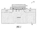
- FIG. 1is a block diagram of an EEPROM structure according to an example embodiment.
- FIG. 2is a block diagram of an EEPROM having extended floating gates according to an example embodiment.
- FIG. 3is a diagram of a capacitor divider model for the EEPROM device of FIG. 2 according to an example embodiment.
- FIG. 4is a cross section o the EEPROM of FIG. 2 taken along line 4 - 4 .
- FIG. 5illustrates typical threshold voltage characteristics for different EEPROMs according to an example embodiment.
- FIG. 6illustrates typical threshold voltage characteristics for different EEPROMs according to an example embodiment.
- FIG. 7illustrates time characteristics with different poling biases according to an example embodiment.
- FIG. 8illustrates measurement of a pressure effect according to an example embodiment.
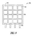
- FIG. 9is a representation of a pixel layout according to an example embodiment.
- Charge-base universal sensors for chemicals, molecules, pressure, and lightcan be mass produced with a simple post processing of the function-specific coating in standard CMOS processes.
- the various sensors and associated pixel circuits as shown in an array 900 in FIG. 9may share the same CMOS chip and the specific sensor function is achieved by the post processing coating. Tight integration with CMOS pixel circuits also allows better sensitivity, bandwidth and low power operations.
- Top metal pixels 910are in contact with a sense coating 920 in one embodiment.
- Readout ports 930provide a mechanism to obtain information about the state of the sense coating in the presence of a desired parameter or parameters to be sensed.
- binding wiressuch as a metal binding wire illustrated at 940 may be coupled to the metal pixels 910 , and then sense coated for applications such as in vivo biomedical sensing.
- Array 900may be one dimensional or two dimensional in various embodiments. Even three dimensional arrays may be formed in further embodiments.
- an extended floating gate (FG) of a MOSFETmetal-oxide semiconductor field-effect transistor
- FGextended floating gate
- MOSFETmetal-oxide semiconductor field-effect transistor
- a control gatethe MOS channel
- a sensing gatewhich can be led out to top metal pixels in physical contact with a post-processing sensing coating.
- the change in the sensing coatingeither as an outer Helmholtz potential ( ⁇ OHP ), diffusive capacitive load C DIF or effective polarization, will be reflected on nonlinear MOS channel IV curves according to governing equations.
- ⁇ OHPouter Helmholtz potential
- DIFdiffusive capacitive load
- effective polarizationthe change in the sensing coating, either as an outer Helmholtz potential ( ⁇ OHP ), diffusive capacitive load C DIF or effective polarization, will be reflected on nonlinear MOS channel IV curves according to governing equations.
- a nonlinear drain currentgives additional design freedom in the trade-off of sensitivity and
- the sensing coatingis a polymer electret film.
- An electretis a dielectric material exhibiting a quasi-permanent electrostatic charge or charge dipole.
- the electret chargecan be the combination of surface charges, space charges, and charge polarization.
- space-charge in electretscan be achieved by injecting carriers from discharging or particle beams.
- Other methodsconsist of carrier generation within the dielectric by light, radiation or heat with simultaneous charge separation by an electric field.
- Dipolar electretscan be often obtained by application of a high electric field at room temperature.
- the MOSFETis an EEPROM (Electrically Erasable Programmable Read Only Memory) device with an extended floating gate.
- the charges in the polymer electret filmare capacitively coupled to the floating gate, in the same manner of the conventional control gate directly driven by biases.
- the polymer electret filmsits on a sensing gate electrically isolated from the floating gate by a dielectric.
- the net charge density in the polymer film weighted by the distance to the sensing gatewill influence the potential on the floating gate. Accordingly, the threshold voltage of the EEPROM device at the control gate will change and can be correlated to the electret charge density.
- FIG. 1shows a basic EEPROM structure 100 with a substrate 105 having n-type source 110 and drain 115 .
- the device 100is similar to a traditional MOSFET except that an extra electrically floating conductor layer 120 is sandwiched between the control gate 125 and the channel 130 .
- Oxide or other insulating layers 135 and 140separate the gate 125 , floating gate 120 and channel 130 respectively.
- the static charge stored in the floating gate 120has over 10-year lifetime and will influence the threshold voltage of the MOSFET channel 130 , which is used to distinguish the stored binary information.
- the channel hot carrier injectionis illustrated in FIG. 1 , which is performed by applying a high voltage on the control gate 125 (usually around 12V) and drain 115 ( ⁇ 6V) terminals with a grounded source.
- the substrate 105is often grounded or further reverse biased to enhance the injection efficiency.
- electrons 150 with enough kinetic energy to overcome the oxide energy barrier 140will be trapped at the floating gate 120 .
- the trapped negative chargeswill delay channel inversion, which translates into an effective increase in the MOSFET threshold voltage.
- a higher control gate voltageis needed to overcome the effect of the floating-gate 120 charges.
- the erasure operationis performed with the gate 125 grounded and the source 110 at a high voltage, typically also around 12V, when the electrons in the floating gate 120 will leak out through the Fowler-Norhdeim (F-N) tunneling mechanism.
- F-NFowler-Norhdeim
- Different areas of the gate oxide 140are used for programming and erasure in this illustration.
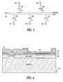
- FIG. 2illustrates a device 200 that utilizes an EEPROM device 205 , 210 to monitor the threshold voltage.
- a first extended floating gateis shown at 215 , with a sensing gate 220 having an electret polymer coating an oxide etch window 225 .
- a second extended gateis shown at 230 , with a sensing gate 235 having an electret polymer coating an oxide etch window 240 .
- the surface area of the second extended floating gate 230is much larger than the surface area of the first extended floating gate 215 .
- the width of the second extended floating gateis larger than approximately 50 ⁇ m.
- the device 200may be fabricated through a MOSIS (Metal Oxide Semiconductor Implementation Service) foundry with a 2-polysilicon and 2-metal process. Different poling methods may be used for devices with different sensing gate areas. Due to the fast and sensitive extraction, real-time monitoring of poling characteristics can be obtained.
- MOSISMetal Oxide Semiconductor Implementation Service
- FIG. 3illustrates a capacitor-divider model for the EEPROM device 200 of FIG. 2 .
- a floating gate 310is connected with many input nodes through different dielectric layers, which is the same as the parallel connection of capacitors from the nodes as illustrated in FIG. 3 .
- the net charge in the floating gateis the sum of the charge in each capacitor.
- V FG at 315is the floating-gate potential.
- V CG 320 , V D 325 , V B 330 , and V S 335are the input signal voltages of control-gate, drain, substrate, and source, respectively.
- V E 340is effective potential on the sensing gate set by the polymer electret film.
- C CG 345 , C S 350 , C D 355 , C B 360 , and C E 365are the capacitive coupling coefficients between the floating gate and each of the input nodes.
- Q FGdenote the net charge in the floating gate
- Q FGC CG ( V FG ⁇ V CG )+ C E ( V FG ⁇ V E )+ C D ( V FG ⁇ V D )+ C B ( V FG ⁇ V B )+ C S ( V FG ⁇ V S ) .
- Q FGis equal to the initial charge on the floating gate, which may be taken as zero at the moment for simplicity. If voltages are measured with respect to the grounded substrate with the source and the substrate being shorted, equation (1) reduces to
- V FG — TH and V CG — THare denoted as the threshold voltages of the EEPROM seen from the floating gate and the control gate, respectively.
- the EEPROMturns on at the condition of V FG >V FG — TH , namely
- Equation (4)is rearranged for V CG as
- V CG> C TOTAL C CG ⁇ V FG ⁇ _ ⁇ TH - C E C CG ⁇ V E - C D C CG ⁇ V D . ( 5 )
- V CG ⁇ _ ⁇ TH iC TOTAL C CG ⁇ V FG ⁇ _ ⁇ TH - C D C CG ⁇ V D . ( 6 )
- V FG — TH in equation (6)shifts to V FG — TH ⁇ Q E /C TOTAL after poling.
- V CG — TH ishifts to V CG — TH f as
- FIG. 4is a cross section of EEPROM 210 with extended floating gate 230 taking along lines 4 - 4 in FIG. 2 .
- EEPROM 210has n-type source and drain with a large extended floating gate 230 , which provides amplified capacitive coupling to the sensing gate 235 .
- An oxide etch window as a post-processing stepis applied to remove a passivation layer on top of the sensing gate.
- Two different extended gate areas in FIG. 2are employed to decouple the parasitic elements.
- the large sensing gate 235has an area of approximately 28,800 ⁇ m 2 , which is ten times larger than the small one. Even smaller areas may be used in further embodiments.
- Post-processing of a polymer coating as illustrated at 410can be done either by direct attachment from pre-made solid polymer films or by dip-coating from polymer solutions.
- an insulatoris formed on top of the control gate, extended floating gate and sensing gate, and the oxide is removed over a portion of the sensing gate to allow contact with the polymer electret sensing coating.
- the portion of removed oxidemay also serve as a portion of a channel for a microfluidic channel to deliver fluid which may contain chemicals to be sensed, or for sensing the pressure exerted by the fluid.
- a covermay be attached to complete the channel.
- the filmmay be a thin film, or may fill up the depression in the oxide shown in FIG. 4 .
- a Teflon® AFpolytetrafluoroethylene amorphous fluoropolymer
- the drying stepis by a hot plate at 130° C. to evaporate the FC75 solvent from 3M.
- the Teflon film thicknessis measured by a profilometer at 60 nm. This is just one example of a process of applying a polymer electret film. Many other methods may be used to obtain coating of desired films of varying thickness.
- the polymer coatingis an electret that is directly coupled to the sensing gate 235 .
- the sensing gate 235is capacitively coupled to the extended floating gate 230 through a dielectric, such as an oxide layer 415 .
- the IV responsesalready show distinctive characteristics in different base solutions where the surface site adsorption (and hence ⁇ OHP ) will affect the threshold voltage V TH and the sensing-gate capacitance C SG will affect the substhreshold slope S.
- extracted C SGalone can be used to distinguish chemical concentration and chemical species, where selectivity in chemical mixture can be achieved from response surface plots, which can reduce the dependence for a fluid reference potential.
- An extracted ⁇ OHP vs. ion concentrations with uncharged floating gateshould have a slope inversely proportional to the number of charge but independent of the chemical species and surface coating. When the floating gate is charged, however, the extracted ⁇ OHP is distinctive to the ion species and coating, which can be used for selectivity enhancement and electrowetting control.
- BSAbovine serum albumin
- lysozymeTwo sample proteins, BSA (bovine serum albumin) and lysozyme are used to demonstrate the molecular sensing capabilities in one example.
- the proteinsare denatured with SDS (sodium dodecyl sulfate), which causes the proteins to unfold by wrapping around the polypeptide backbone.
- SDSbinds to the backbone with a mass ratio of 1.4:1, and in this way confers a negative charge to the protein in proportion to its mass.
- BSA and lysozymeare robust proteins that have significantly different masses of 66.2 kDa and 14.4 kDa, respectively.
- the difference in massesleads to differences in external net charge and, in turn, to differences in the ⁇ OHP and C DIF of the CvMOS device. Distinctive charge and capacitive responses can be observed from the two different molecules when the floating gate is charged with electron injection.
- CvMOScan serve as a pressure sensor.
- a wide range of sensitivitycan be achieved by selecting the pressure effects.
- Teflon AFpolarized by a poling electrical stress, is used for illustration where the sensitivity is in the 10 kPa range.
- mechano-polingis done by applying mechanical pressure on Teflon AF that has gone through photo-poling.
- the original amorphous Teflonis not piezoelectric due to lack of long-range directional order of charge density. However, if Teflon already contains significant space charges, it will demonstrate pressure responses from mechanical strain. For the same characterization structure, a mechanical pressure effect can be accurately determined, which may be used as a charge-based pressure sensor.
- the sensor devicecan function as a pressure sensor with a large tuning range.
- the piezoelectric materialcan be sandwiched between two metal layers, which can also be used as additional grounding electrodes to further stabilize the device response.
- Both inorganic (such as PZT) and organic (PVDF) piezoelectric coatingcan be used, depending on the range of pressure of interest.
- PVDF coatingnot only has the feasible range for sensing, but also can be implemented in a flexible electrode.
- the sensor devicecan function as a temperature sensor.
- Most pyroelectric materialsalso demonstrate piezoelectric responses, and the individual contribution from the pressure and heat can be decoupled from two or more sensing gate with either different coating materials, or different thickness of the same pyroelectric/piezoelectric material.
- Light sensing by CvMOScan be achieved with P3HT photovoltaic polymer coating.
- the polarization of P3HT and hence the IV changesdepend on the wavelength and intensity. Different light sources thus give distinctive IV responses in FIG. 13 . Notice that this is not due to the enhanced leakage of floating gate charges as the IV curve will quickly revert back to the one of charged FG with no light when the light is turned off. Detailed wavelength responses can also be obtained.
- electret charginginvolves photo poling by UV light with high DC biases.
- UV lampswere used to produce 8 W of one of the 254/302/365 nm wavelengths, which is located near the sample on a probe station.
- a plate probe of high voltage during the photo polingis located directly on the polymer film surface and the ground is connected to the substrate.
- This setupwill put a large electric field across the electret polymer film. Further UV illumination will excite electrons and holes in the insulating polymer film traveling in opposite directions by the applied electric field. Some carriers can go out of the external surfaces of the polymer film and the others can be trapped to form space charge.
- UV irradiationhas been verified by applying transparent ITO (Indium-tin Oxide) contacts on the electret film, and found that the electric field uniformity is not a critical factor in photo poling. Dipole polarization can also result from different electron and hole transport properties. Photoelectret equilibrium charge density is mainly governed by the polarizing field intensity, which can be estimated by the product of light intensity and time of polarizing. The samples are erased by 254 nm UV light of 1.6 W for an hour without applied electric fields before all poling tests, which serves as the reference in obtaining threshold voltage difference.
- ITOIndium-tin Oxide
- the results from representative tests with different poling conditionsshow the range and sensitivity of the described characterization method.
- the size difference of the extended gate areais used to de-embed the intrinsic parasitic elements and to obtain a larger range of effective electret charge per unit area.
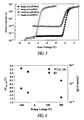
- FIG. 5shows typical threshold voltage characteristics of two EEPROMs with 302 nm UV and a 200V poling voltage.
- the thresholdshifts over a large range and after photopoling.
- Other alternative poling processesmay include pressure poling and corona charging.
- ⁇ V CG — TH with the larger sensing gate areais bigger according to Eq. (8).
- ⁇ V CG — THis not exactly proportional to the ratio of the extended gate areas because the small extended gate area has relatively large parasitic capacitance.
- ⁇ V CG — TH of the two EEPROMs under testare ⁇ 6.0V and ⁇ 0.10V.
- the charge densities ⁇ Eare 7.66 ⁇ 10 ⁇ 9 coul/cm 2 and 1.27 ⁇ 10 ⁇ 10 coul/cm 2 of positive charges for the large and small sensing gates, respectively.
- the difference in charge densitycan be explained by the UV shadowing and film thickness variation in the smaller sensing gate.
- the anomalous high current in the deep subthreshold region (V CG ⁇ 1.0V) in the small sensing gate caseis repeatable and does not appear before the Teflon coating.
- FIG. 6shows the threshold voltage characteristics of the EEPROM device with different poling voltages, ⁇ 50V, ⁇ 100V, and 200V.
- the changes of the threshold voltageare 0.448V, 0.262V, and ⁇ 1.152V, respectively, which correspond to the charge densities ⁇ E in the polymer film as ⁇ 5.72 ⁇ 10 ⁇ 10 , ⁇ 3.35 ⁇ 10 ⁇ 10 and 1.47 ⁇ 10 ⁇ 9 coul/cm 2 respectively.
- the polarity and magnitude of the extracted charge density under different poling biasesagree well with the expected values of the Teflon AF.
- FIG. 7shows the time characteristics of ⁇ V CG — TH with different poling biases.
- the shift of the threshold voltageis saturated after 15 minutes poling application.
- ⁇ V CG — THsaturates in 2-3 minutes.
- the effective charge densitywill saturate because the electric field within the electret film will decrease with the generation of static charges or charge dipoles during the poling process.
- FIG. 8illustrates the measurements of a pressure effect.
- the Teflon AF on the sensing gateis subject to mechanical pressure.
- the originally nonpolar Teflon AF filmwill be polarized after the photo poling process with residual charges, which will continuously change with further mechanical strain.
- FIG. 8shows the time characteristics of ⁇ V CG — TH when pressure is applied to the Teflon AF film after the photo poling procedure.
- the changes of the threshold voltage of each pressureare ⁇ 0.176V, ⁇ 0.246V and ⁇ 0.356V after 10 minutes of applied pressure.
- the effective charge densitiesare 2.25 ⁇ 10 ⁇ 10 coul/cm 2 , 3.14 ⁇ 10 ⁇ 10 coul/cm 2 and 4.55 ⁇ 10 ⁇ 10 coul/cm 2 of positive charges for 0.0176 MPa, 0.0301 MPa, and 0.0478 MPa, respectively.
- an electret on an extended floating gate of a transistorprovides a charge based approach to sensing multiple different parameters on a single substrate.
- the use of a polymer electretallows for post circuit processes to form a multitude of different sensors by using different polymers that are compatible with the formed circuitry.
Landscapes
- Life Sciences & Earth Sciences (AREA)
- Chemical & Material Sciences (AREA)
- Health & Medical Sciences (AREA)
- Physics & Mathematics (AREA)
- Biochemistry (AREA)
- Microelectronics & Electronic Packaging (AREA)
- Chemical Kinetics & Catalysis (AREA)
- Electrochemistry (AREA)
- Engineering & Computer Science (AREA)
- Analytical Chemistry (AREA)
- Molecular Biology (AREA)
- General Health & Medical Sciences (AREA)
- General Physics & Mathematics (AREA)
- Immunology (AREA)
- Pathology (AREA)
- Pressure Sensors (AREA)
- Investigating Or Analyzing Materials By The Use Of Electric Means (AREA)
Abstract
Description
QFG=CCG(VFG−VCG)+CE(VFG−VE)+CD(VFG−VD)+CB(VFG−VB)+CS(VFG−VS) . (1)
Equation (4) is rearranged for VCGas
ρE=QE/ASG=−ΔVCG
where ASGis the area of the sensing gate.
Claims (11)
Priority Applications (1)
| Application Number | Priority Date | Filing Date | Title |
|---|---|---|---|
| US11/862,867US7960776B2 (en) | 2006-09-27 | 2007-09-27 | Transistor with floating gate and electret |
Applications Claiming Priority (2)
| Application Number | Priority Date | Filing Date | Title |
|---|---|---|---|
| US84751606P | 2006-09-27 | 2006-09-27 | |
| US11/862,867US7960776B2 (en) | 2006-09-27 | 2007-09-27 | Transistor with floating gate and electret |
Publications (2)
| Publication Number | Publication Date |
|---|---|
| US20080094074A1 US20080094074A1 (en) | 2008-04-24 |
| US7960776B2true US7960776B2 (en) | 2011-06-14 |
Family
ID=39317302
Family Applications (1)
| Application Number | Title | Priority Date | Filing Date |
|---|---|---|---|
| US11/862,867Expired - Fee RelatedUS7960776B2 (en) | 2006-09-27 | 2007-09-27 | Transistor with floating gate and electret |
Country Status (1)
| Country | Link |
|---|---|
| US (1) | US7960776B2 (en) |
Cited By (35)
| Publication number | Priority date | Publication date | Assignee | Title |
|---|---|---|---|---|
| US8841217B1 (en) | 2013-03-13 | 2014-09-23 | Life Technologies Corporation | Chemical sensor with protruded sensor surface |
| US8858782B2 (en) | 2010-06-30 | 2014-10-14 | Life Technologies Corporation | Ion-sensing charge-accumulation circuits and methods |
| US8912005B1 (en) | 2010-09-24 | 2014-12-16 | Life Technologies Corporation | Method and system for delta double sampling |
| US8912580B2 (en) | 2009-05-29 | 2014-12-16 | Life Technologies Corporation | Active chemically-sensitive sensors with in-sensor current sources |
| US8936763B2 (en) | 2008-10-22 | 2015-01-20 | Life Technologies Corporation | Integrated sensor arrays for biological and chemical analysis |
| US8963216B2 (en) | 2013-03-13 | 2015-02-24 | Life Technologies Corporation | Chemical sensor with sidewall spacer sensor surface |
| US8962366B2 (en) | 2013-01-28 | 2015-02-24 | Life Technologies Corporation | Self-aligned well structures for low-noise chemical sensors |
| US9023189B2 (en) | 2006-12-14 | 2015-05-05 | Life Technologies Corporation | High density sensor array without wells |
| US9080968B2 (en) | 2013-01-04 | 2015-07-14 | Life Technologies Corporation | Methods and systems for point of use removal of sacrificial material |
| US9116117B2 (en) | 2013-03-15 | 2015-08-25 | Life Technologies Corporation | Chemical sensor with sidewall sensor surface |
| US9128044B2 (en) | 2013-03-15 | 2015-09-08 | Life Technologies Corporation | Chemical sensors with consistent sensor surface areas |
| US9164070B2 (en) | 2010-06-30 | 2015-10-20 | Life Technologies Corporation | Column adc |
| US9194000B2 (en) | 2008-06-25 | 2015-11-24 | Life Technologies Corporation | Methods and apparatus for measuring analytes using large scale FET arrays |
| US9269708B2 (en) | 2006-12-14 | 2016-02-23 | Life Technologies Corporation | Methods and apparatus for measuring analytes using large scale FET arrays |
| US9270264B2 (en) | 2012-05-29 | 2016-02-23 | Life Technologies Corporation | System for reducing noise in a chemical sensor array |
| US9404920B2 (en) | 2006-12-14 | 2016-08-02 | Life Technologies Corporation | Methods and apparatus for detecting molecular interactions using FET arrays |
| US9600208B2 (en) | 2014-11-21 | 2017-03-21 | Palo Alto Research Center Incorporated | Passive detector with nonvolatile memory storage |
| US9618475B2 (en) | 2010-09-15 | 2017-04-11 | Life Technologies Corporation | Methods and apparatus for measuring analytes |
| US9671363B2 (en) | 2013-03-15 | 2017-06-06 | Life Technologies Corporation | Chemical sensor with consistent sensor surface areas |
| US9823217B2 (en) | 2013-03-15 | 2017-11-21 | Life Technologies Corporation | Chemical device with thin conductive element |
| US9835585B2 (en) | 2013-03-15 | 2017-12-05 | Life Technologies Corporation | Chemical sensor with protruded sensor surface |
| US9841398B2 (en) | 2013-01-08 | 2017-12-12 | Life Technologies Corporation | Methods for manufacturing well structures for low-noise chemical sensors |
| US9927393B2 (en) | 2009-05-29 | 2018-03-27 | Life Technologies Corporation | Methods and apparatus for measuring analytes |
| US9960253B2 (en) | 2010-07-03 | 2018-05-01 | Life Technologies Corporation | Chemically sensitive sensor with lightly doped drains |
| US9970984B2 (en) | 2011-12-01 | 2018-05-15 | Life Technologies Corporation | Method and apparatus for identifying defects in a chemical sensor array |
| US10077472B2 (en) | 2014-12-18 | 2018-09-18 | Life Technologies Corporation | High data rate integrated circuit with power management |
| US10100357B2 (en) | 2013-05-09 | 2018-10-16 | Life Technologies Corporation | Windowed sequencing |
| US10309924B2 (en) | 2013-06-07 | 2019-06-04 | Cornell University | Floating gate based sensor apparatus and related floating gate based sensor applications |
| US10379079B2 (en) | 2014-12-18 | 2019-08-13 | Life Technologies Corporation | Methods and apparatus for measuring analytes using large scale FET arrays |
| US10451585B2 (en) | 2009-05-29 | 2019-10-22 | Life Technologies Corporation | Methods and apparatus for measuring analytes |
| US10458942B2 (en) | 2013-06-10 | 2019-10-29 | Life Technologies Corporation | Chemical sensor array having multiple sensors per well |
| US10605767B2 (en) | 2014-12-18 | 2020-03-31 | Life Technologies Corporation | High data rate integrated circuit with transmitter configuration |
| US11231451B2 (en) | 2010-06-30 | 2022-01-25 | Life Technologies Corporation | Methods and apparatus for testing ISFET arrays |
| US11307166B2 (en) | 2010-07-01 | 2022-04-19 | Life Technologies Corporation | Column ADC |
| US11339430B2 (en) | 2007-07-10 | 2022-05-24 | Life Technologies Corporation | Methods and apparatus for measuring analytes using large scale FET arrays |
Families Citing this family (10)
| Publication number | Priority date | Publication date | Assignee | Title |
|---|---|---|---|---|
| WO2010014283A1 (en)* | 2008-07-30 | 2010-02-04 | Max Power Semiconductor Inc. | Lateral devices containing permanent charge |
| US20110137184A1 (en)* | 2008-08-19 | 2011-06-09 | Fan Ren | Pressure sensing |
| EP2342552B1 (en)* | 2008-10-22 | 2022-09-14 | Life Technologies Corporation | Floating gate chemical field effect transistor array with bilayer gate dielectric |
| FR2952183A1 (en)* | 2009-10-30 | 2011-05-06 | St Microelectronics Crolles 2 | DETECTOR OF BIOLOGICAL OR CHEMICAL MATERIAL AND CORRESPONDING DETECTOR MATRIX |
| US8878257B2 (en) | 2010-06-04 | 2014-11-04 | Freescale Semiconductor, Inc. | Methods and apparatus for an ISFET |
| GB2484339B (en)* | 2010-10-08 | 2016-12-21 | Dnae Group Holdings Ltd | Electrostatic discharge protection |
| JP6309734B2 (en)* | 2013-10-04 | 2018-04-11 | 株式会社日立ハイテクノロジーズ | Biomolecule measuring device |
| US9423376B2 (en) | 2014-04-30 | 2016-08-23 | Freescale Semiconductor, Inc. | Differential pair sensing circuit structures |
| EP3176574B1 (en)* | 2015-12-02 | 2021-01-27 | Emberion Oy | A sensor apparatus and associated methods |
| DE102019114130A1 (en)* | 2019-05-27 | 2020-12-03 | Christian-Albrechts-Universität Zu Kiel | Electrical component and method for sensing mechanical deformation |
Citations (6)
| Publication number | Priority date | Publication date | Assignee | Title |
|---|---|---|---|---|
| US4851682A (en) | 1987-03-20 | 1989-07-25 | Kureha Kagaku Kogyo Kabushiki Kaisha | Pyroelectric infrared sensor |
| US6141243A (en) | 1996-11-12 | 2000-10-31 | Fraunhofer-Gesellschaft Zur Forderung Der Angewandten Forschung E.V. | Sensor element |
| US20050230271A1 (en) | 2004-01-12 | 2005-10-20 | Kalle Levon | Floating gate field effect transistors for chemical and/or biological sensing |
| US7053439B2 (en)* | 2002-10-29 | 2006-05-30 | Edwin Kan | Chemoreceptive semiconductor structure |
| US7186380B2 (en)* | 2002-07-01 | 2007-03-06 | Hewlett-Packard Development Company, L.P. | Transistor and sensors made from molecular materials with electric dipoles |
| US20070254455A1 (en)* | 2006-04-28 | 2007-11-01 | Semiconductor Energy Laboratory Co., Ltd. | Semiconductor integrated circuit, manufacturing method thereof, and semiconductor device using semiconductor integrated circuit |
- 2007
- 2007-09-27USUS11/862,867patent/US7960776B2/ennot_activeExpired - Fee Related
Patent Citations (7)
| Publication number | Priority date | Publication date | Assignee | Title |
|---|---|---|---|---|
| US4851682A (en) | 1987-03-20 | 1989-07-25 | Kureha Kagaku Kogyo Kabushiki Kaisha | Pyroelectric infrared sensor |
| US6141243A (en) | 1996-11-12 | 2000-10-31 | Fraunhofer-Gesellschaft Zur Forderung Der Angewandten Forschung E.V. | Sensor element |
| US7186380B2 (en)* | 2002-07-01 | 2007-03-06 | Hewlett-Packard Development Company, L.P. | Transistor and sensors made from molecular materials with electric dipoles |
| US7053439B2 (en)* | 2002-10-29 | 2006-05-30 | Edwin Kan | Chemoreceptive semiconductor structure |
| US20050230271A1 (en) | 2004-01-12 | 2005-10-20 | Kalle Levon | Floating gate field effect transistors for chemical and/or biological sensing |
| US7462512B2 (en)* | 2004-01-12 | 2008-12-09 | Polytechnic University | Floating gate field effect transistors for chemical and/or biological sensing |
| US20070254455A1 (en)* | 2006-04-28 | 2007-11-01 | Semiconductor Energy Laboratory Co., Ltd. | Semiconductor integrated circuit, manufacturing method thereof, and semiconductor device using semiconductor integrated circuit |
Non-Patent Citations (2)
| Title |
|---|
| Berry, R. B., et al., "Comparison of respiratory event detection by a polyvinylidene fluoride film airflow sensor and a pneumotachograph in sleep apnea patients.", Chest, 128(3), (Sep. 2005),1331-8. |
| Kressmann, R. , et al., "Space-charge Electrets", IEEE Transactions on Dielectrics and Electrical Insulation, 3(5), (Oct. 1996),607-623. |
Cited By (86)
| Publication number | Priority date | Publication date | Assignee | Title |
|---|---|---|---|---|
| US10502708B2 (en) | 2006-12-14 | 2019-12-10 | Life Technologies Corporation | Chemically-sensitive sensor array calibration circuitry |
| US11732297B2 (en)* | 2006-12-14 | 2023-08-22 | Life Technologies Corporation | Methods and apparatus for measuring analytes using large scale FET arrays |
| US20220340965A1 (en)* | 2006-12-14 | 2022-10-27 | Life Technologies Corporation | Methods and Apparatus for Measuring Analytes Using Large Scale FET Arrays |
| US12140560B2 (en) | 2006-12-14 | 2024-11-12 | Life Technologies Corporation | Methods and apparatus for measuring analytes using large scale FET arrays |
| US10203300B2 (en) | 2006-12-14 | 2019-02-12 | Life Technologies Corporation | Methods and apparatus for measuring analytes using large scale FET arrays |
| US12066399B2 (en) | 2006-12-14 | 2024-08-20 | Life Technologies Corporation | Methods and apparatus for measuring analytes using large scale FET arrays |
| US11435314B2 (en) | 2006-12-14 | 2022-09-06 | Life Technologies Corporation | Chemically-sensitive sensor array device |
| US9951382B2 (en) | 2006-12-14 | 2018-04-24 | Life Technologies Corporation | Methods and apparatus for measuring analytes using large scale FET arrays |
| US9023189B2 (en) | 2006-12-14 | 2015-05-05 | Life Technologies Corporation | High density sensor array without wells |
| US10415079B2 (en) | 2006-12-14 | 2019-09-17 | Life Technologies Corporation | Methods and apparatus for detecting molecular interactions using FET arrays |
| US9989489B2 (en) | 2006-12-14 | 2018-06-05 | Life Technnologies Corporation | Methods for calibrating an array of chemically-sensitive sensors |
| US10633699B2 (en) | 2006-12-14 | 2020-04-28 | Life Technologies Corporation | Methods and apparatus for measuring analytes using large scale FET arrays |
| US9404920B2 (en) | 2006-12-14 | 2016-08-02 | Life Technologies Corporation | Methods and apparatus for detecting molecular interactions using FET arrays |
| US9134269B2 (en) | 2006-12-14 | 2015-09-15 | Life Technologies Corporation | Methods and apparatus for measuring analytes using large scale FET arrays |
| US10816506B2 (en) | 2006-12-14 | 2020-10-27 | Life Technologies Corporation | Method for measuring analytes using large scale chemfet arrays |
| US9269708B2 (en) | 2006-12-14 | 2016-02-23 | Life Technologies Corporation | Methods and apparatus for measuring analytes using large scale FET arrays |
| US11339430B2 (en) | 2007-07-10 | 2022-05-24 | Life Technologies Corporation | Methods and apparatus for measuring analytes using large scale FET arrays |
| US9194000B2 (en) | 2008-06-25 | 2015-11-24 | Life Technologies Corporation | Methods and apparatus for measuring analytes using large scale FET arrays |
| US11137369B2 (en) | 2008-10-22 | 2021-10-05 | Life Technologies Corporation | Integrated sensor arrays for biological and chemical analysis |
| US11874250B2 (en) | 2008-10-22 | 2024-01-16 | Life Technologies Corporation | Integrated sensor arrays for biological and chemical analysis |
| US12146853B2 (en) | 2008-10-22 | 2024-11-19 | Life Technologies Corporation | Methods and apparatus including array of reaction chambers over array of chemFET sensors for measuring analytes |
| US9964515B2 (en) | 2008-10-22 | 2018-05-08 | Life Technologies Corporation | Integrated sensor arrays for biological and chemical analysis |
| US8936763B2 (en) | 2008-10-22 | 2015-01-20 | Life Technologies Corporation | Integrated sensor arrays for biological and chemical analysis |
| US11448613B2 (en) | 2008-10-22 | 2022-09-20 | Life Technologies Corporation | ChemFET sensor array including overlying array of wells |
| US9944981B2 (en) | 2008-10-22 | 2018-04-17 | Life Technologies Corporation | Methods and apparatus for measuring analytes |
| US10451585B2 (en) | 2009-05-29 | 2019-10-22 | Life Technologies Corporation | Methods and apparatus for measuring analytes |
| US10809226B2 (en) | 2009-05-29 | 2020-10-20 | Life Technologies Corporation | Methods and apparatus for measuring analytes |
| US9927393B2 (en) | 2009-05-29 | 2018-03-27 | Life Technologies Corporation | Methods and apparatus for measuring analytes |
| US12038405B2 (en) | 2009-05-29 | 2024-07-16 | Life Technologies Corporation | Methods and apparatus for measuring analytes |
| US8994076B2 (en) | 2009-05-29 | 2015-03-31 | Life Technologies Corporation | Chemically-sensitive field effect transistor based pixel array with protection diodes |
| US11692964B2 (en) | 2009-05-29 | 2023-07-04 | Life Technologies Corporation | Methods and apparatus for measuring analytes |
| US11768171B2 (en) | 2009-05-29 | 2023-09-26 | Life Technologies Corporation | Methods and apparatus for measuring analytes |
| US8912580B2 (en) | 2009-05-29 | 2014-12-16 | Life Technologies Corporation | Active chemically-sensitive sensors with in-sensor current sources |
| US10718733B2 (en) | 2009-05-29 | 2020-07-21 | Life Technologies Corporation | Methods and apparatus for measuring analytes |
| US12038406B2 (en) | 2010-06-30 | 2024-07-16 | Life Technologies Corporation | Semiconductor-based chemical detection device |
| US11231451B2 (en) | 2010-06-30 | 2022-01-25 | Life Technologies Corporation | Methods and apparatus for testing ISFET arrays |
| US10481123B2 (en) | 2010-06-30 | 2019-11-19 | Life Technologies Corporation | Ion-sensing charge-accumulation circuits and methods |
| US8858782B2 (en) | 2010-06-30 | 2014-10-14 | Life Technologies Corporation | Ion-sensing charge-accumulation circuits and methods |
| US10641729B2 (en) | 2010-06-30 | 2020-05-05 | Life Technologies Corporation | Column ADC |
| US9239313B2 (en) | 2010-06-30 | 2016-01-19 | Life Technologies Corporation | Ion-sensing charge-accumulation circuits and methods |
| US9164070B2 (en) | 2010-06-30 | 2015-10-20 | Life Technologies Corporation | Column adc |
| US11307166B2 (en) | 2010-07-01 | 2022-04-19 | Life Technologies Corporation | Column ADC |
| US9960253B2 (en) | 2010-07-03 | 2018-05-01 | Life Technologies Corporation | Chemically sensitive sensor with lightly doped drains |
| US9958415B2 (en) | 2010-09-15 | 2018-05-01 | Life Technologies Corporation | ChemFET sensor including floating gate |
| US9618475B2 (en) | 2010-09-15 | 2017-04-11 | Life Technologies Corporation | Methods and apparatus for measuring analytes |
| US12050195B2 (en) | 2010-09-15 | 2024-07-30 | Life Technologies Corporation | Methods and apparatus for measuring analytes using chemfet arrays |
| US9958414B2 (en) | 2010-09-15 | 2018-05-01 | Life Technologies Corporation | Apparatus for measuring analytes including chemical sensor array |
| US9110015B2 (en) | 2010-09-24 | 2015-08-18 | Life Technologies Corporation | Method and system for delta double sampling |
| US8912005B1 (en) | 2010-09-24 | 2014-12-16 | Life Technologies Corporation | Method and system for delta double sampling |
| US10598723B2 (en) | 2011-12-01 | 2020-03-24 | Life Technologies Corporation | Method and apparatus for identifying defects in a chemical sensor array |
| US10365321B2 (en) | 2011-12-01 | 2019-07-30 | Life Technologies Corporation | Method and apparatus for identifying defects in a chemical sensor array |
| US9970984B2 (en) | 2011-12-01 | 2018-05-15 | Life Technologies Corporation | Method and apparatus for identifying defects in a chemical sensor array |
| US10404249B2 (en) | 2012-05-29 | 2019-09-03 | Life Technologies Corporation | System for reducing noise in a chemical sensor array |
| US9270264B2 (en) | 2012-05-29 | 2016-02-23 | Life Technologies Corporation | System for reducing noise in a chemical sensor array |
| US9985624B2 (en) | 2012-05-29 | 2018-05-29 | Life Technologies Corporation | System for reducing noise in a chemical sensor array |
| US9080968B2 (en) | 2013-01-04 | 2015-07-14 | Life Technologies Corporation | Methods and systems for point of use removal of sacrificial material |
| US9852919B2 (en) | 2013-01-04 | 2017-12-26 | Life Technologies Corporation | Methods and systems for point of use removal of sacrificial material |
| US9841398B2 (en) | 2013-01-08 | 2017-12-12 | Life Technologies Corporation | Methods for manufacturing well structures for low-noise chemical sensors |
| US10436742B2 (en) | 2013-01-08 | 2019-10-08 | Life Technologies Corporation | Methods for manufacturing well structures for low-noise chemical sensors |
| US8962366B2 (en) | 2013-01-28 | 2015-02-24 | Life Technologies Corporation | Self-aligned well structures for low-noise chemical sensors |
| US8841217B1 (en) | 2013-03-13 | 2014-09-23 | Life Technologies Corporation | Chemical sensor with protruded sensor surface |
| US9995708B2 (en) | 2013-03-13 | 2018-06-12 | Life Technologies Corporation | Chemical sensor with sidewall spacer sensor surface |
| US8963216B2 (en) | 2013-03-13 | 2015-02-24 | Life Technologies Corporation | Chemical sensor with sidewall spacer sensor surface |
| US10422767B2 (en) | 2013-03-15 | 2019-09-24 | Life Technologies Corporation | Chemical sensor with consistent sensor surface areas |
| US10481124B2 (en) | 2013-03-15 | 2019-11-19 | Life Technologies Corporation | Chemical device with thin conductive element |
| US9671363B2 (en) | 2013-03-15 | 2017-06-06 | Life Technologies Corporation | Chemical sensor with consistent sensor surface areas |
| US9116117B2 (en) | 2013-03-15 | 2015-08-25 | Life Technologies Corporation | Chemical sensor with sidewall sensor surface |
| US9823217B2 (en) | 2013-03-15 | 2017-11-21 | Life Technologies Corporation | Chemical device with thin conductive element |
| US9128044B2 (en) | 2013-03-15 | 2015-09-08 | Life Technologies Corporation | Chemical sensors with consistent sensor surface areas |
| US9835585B2 (en) | 2013-03-15 | 2017-12-05 | Life Technologies Corporation | Chemical sensor with protruded sensor surface |
| US11028438B2 (en) | 2013-05-09 | 2021-06-08 | Life Technologies Corporation | Windowed sequencing |
| US10100357B2 (en) | 2013-05-09 | 2018-10-16 | Life Technologies Corporation | Windowed sequencing |
| US10655175B2 (en) | 2013-05-09 | 2020-05-19 | Life Technologies Corporation | Windowed sequencing |
| US10309924B2 (en) | 2013-06-07 | 2019-06-04 | Cornell University | Floating gate based sensor apparatus and related floating gate based sensor applications |
| US10962501B2 (en) | 2013-06-07 | 2021-03-30 | Cornell University | Floating gate based sensor apparatus and related floating gate based sensor applications |
| US11499938B2 (en) | 2013-06-10 | 2022-11-15 | Life Technologies Corporation | Chemical sensor array having multiple sensors per well |
| US11774401B2 (en) | 2013-06-10 | 2023-10-03 | Life Technologies Corporation | Chemical sensor array having multiple sensors per well |
| US10816504B2 (en) | 2013-06-10 | 2020-10-27 | Life Technologies Corporation | Chemical sensor array having multiple sensors per well |
| US10458942B2 (en) | 2013-06-10 | 2019-10-29 | Life Technologies Corporation | Chemical sensor array having multiple sensors per well |
| US9600208B2 (en) | 2014-11-21 | 2017-03-21 | Palo Alto Research Center Incorporated | Passive detector with nonvolatile memory storage |
| US11536688B2 (en) | 2014-12-18 | 2022-12-27 | Life Technologies Corporation | High data rate integrated circuit with transmitter configuration |
| US10767224B2 (en) | 2014-12-18 | 2020-09-08 | Life Technologies Corporation | High data rate integrated circuit with power management |
| US10605767B2 (en) | 2014-12-18 | 2020-03-31 | Life Technologies Corporation | High data rate integrated circuit with transmitter configuration |
| US10379079B2 (en) | 2014-12-18 | 2019-08-13 | Life Technologies Corporation | Methods and apparatus for measuring analytes using large scale FET arrays |
| US10077472B2 (en) | 2014-12-18 | 2018-09-18 | Life Technologies Corporation | High data rate integrated circuit with power management |
| US12196704B2 (en) | 2014-12-18 | 2025-01-14 | Life Technologies Corporation | High data rate integrated circuit with transmitter configuration |
Also Published As
| Publication number | Publication date |
|---|---|
| US20080094074A1 (en) | 2008-04-24 |
Similar Documents
| Publication | Publication Date | Title |
|---|---|---|
| US7960776B2 (en) | Transistor with floating gate and electret | |
| Kressmann et al. | Space-charge electrets | |
| US20240377352A1 (en) | High sensitivity isfet sensor | |
| US7053439B2 (en) | Chemoreceptive semiconductor structure | |
| US10132773B2 (en) | Using floating gate field effect transistors for chemical and/or biological sensing | |
| US5712816A (en) | Method for evaluating the dielectric layer of nonvolatile EPROM, EEPROM and flash-EEPROM memories | |
| JP2000505947A (en) | Memory device using proton transfer | |
| JPH077140A (en) | Evaluating method and testing equipment for gate oxide layer of nonvolatile memory | |
| EP3217167B1 (en) | Humidity sensors with transistor structures and piezoelectric layer | |
| EP3657165A1 (en) | Method for providing calibration data for a gas sensor device, method of calibrating a gas sensor device, and processing device for a gas sensor device | |
| Buitrago et al. | Electrical characterization of high performance, liquid gated vertically stacked SiNW-based 3D FET biosensors | |
| US6762453B1 (en) | Programmable memory transistor | |
| CN1320622C (en) | Semiconductor element and system, wafers, its use and measuring method | |
| US20080023699A1 (en) | A test structure and method for detecting charge effects during semiconductor processing | |
| US7858975B2 (en) | Organic field effect transistor systems and methods | |
| De Nardi et al. | Direct measurements of charge in floating gate transistor channels of flash memories using scanning capacitance microscopy | |
| Al-Ahdal et al. | ISFET threshold voltage programming in CMOS using electron tunnelling | |
| JPS5886777A (en) | Setting method for threshold voltage of mnos memory cell | |
| Lai et al. | A CMOS biocompatible charge detector for biosensing applications | |
| Honda et al. | Visualization of electrons and holes localized in the thin gate film ofmetal-oxide-nitride-oxide-semiconductor type Flash memory by scanning nonlineardielectric microscopy | |
| US20080258179A1 (en) | Hybrid molecular electronic device for switching, memory, and sensor applications, and method of fabricating same | |
| Tareq et al. | An extended floating gate gas sensor using polypyrrole as a sensing polymer | |
| Kim et al. | Fast and sensitive electret polymer characterization by extended floating gate MOSFET | |
| KR101878848B1 (en) | Biosensor based on field-effect transistor having multi-dielectric stack and fabrication method thereof | |
| Sikora et al. | Technologies and reliability of modern embedded flash cells |
Legal Events
| Date | Code | Title | Description |
|---|---|---|---|
| AS | Assignment | Owner name:CORNELL RESEARCH FOUNDATION, INC, NEW YORK Free format text:ASSIGNMENT OF ASSIGNORS INTEREST;ASSIGNORS:KIM, MYONGSEOB;SHEN, NICK YU-MIN;LEE, CHUNGHO;AND OTHERS;REEL/FRAME:020326/0069;SIGNING DATES FROM 20071113 TO 20071221 Owner name:CORNELL RESEARCH FOUNDATION, INC, NEW YORK Free format text:ASSIGNMENT OF ASSIGNORS INTEREST;ASSIGNORS:KIM, MYONGSEOB;SHEN, NICK YU-MIN;LEE, CHUNGHO;AND OTHERS;SIGNING DATES FROM 20071113 TO 20071221;REEL/FRAME:020326/0069 | |
| FEPP | Fee payment procedure | Free format text:PAYOR NUMBER ASSIGNED (ORIGINAL EVENT CODE: ASPN); ENTITY STATUS OF PATENT OWNER: SMALL ENTITY | |
| STCF | Information on status: patent grant | Free format text:PATENTED CASE | |
| AS | Assignment | Owner name:NATIONAL SCIENCE FOUNDATION, VIRGINIA Free format text:CONFIRMATORY LICENSE;ASSIGNOR:CORNELL UNIVERSITY;REEL/FRAME:026733/0194 Effective date:20110803 | |
| FPAY | Fee payment | Year of fee payment:4 | |
| MAFP | Maintenance fee payment | Free format text:PAYMENT OF MAINTENANCE FEE, 8TH YR, SMALL ENTITY (ORIGINAL EVENT CODE: M2552); ENTITY STATUS OF PATENT OWNER: SMALL ENTITY Year of fee payment:8 | |
| FEPP | Fee payment procedure | Free format text:MAINTENANCE FEE REMINDER MAILED (ORIGINAL EVENT CODE: REM.); ENTITY STATUS OF PATENT OWNER: SMALL ENTITY | |
| LAPS | Lapse for failure to pay maintenance fees | Free format text:PATENT EXPIRED FOR FAILURE TO PAY MAINTENANCE FEES (ORIGINAL EVENT CODE: EXP.); ENTITY STATUS OF PATENT OWNER: SMALL ENTITY | |
| STCH | Information on status: patent discontinuation | Free format text:PATENT EXPIRED DUE TO NONPAYMENT OF MAINTENANCE FEES UNDER 37 CFR 1.362 | |
| FP | Lapsed due to failure to pay maintenance fee | Effective date:20230614 |