US7957805B2 - Implantable microstimulator with external electrodes disposed on a film substrate and methods of manufacture and use - Google Patents
Implantable microstimulator with external electrodes disposed on a film substrate and methods of manufacture and useDownload PDFInfo
- Publication number
- US7957805B2 US7957805B2US11/142,154US14215405AUS7957805B2US 7957805 B2US7957805 B2US 7957805B2US 14215405 AUS14215405 AUS 14215405AUS 7957805 B2US7957805 B2US 7957805B2
- Authority
- US
- United States
- Prior art keywords
- housing
- film substrate
- electrodes
- disposed
- vias
- Prior art date
- Legal status (The legal status is an assumption and is not a legal conclusion. Google has not performed a legal analysis and makes no representation as to the accuracy of the status listed.)
- Expired - Fee Related, expires
Links
- 239000000758substrateSubstances0.000titleclaimsabstractdescription87
- 238000000034methodMethods0.000titleclaimsdescription19
- 238000004519manufacturing processMethods0.000titleclaimsdescription11
- 239000004020conductorSubstances0.000claimsdescription27
- 229910052751metalInorganic materials0.000claimsdescription15
- 239000002184metalSubstances0.000claimsdescription15
- 239000000463materialSubstances0.000claimsdescription13
- 230000008878couplingEffects0.000claimsdescription9
- 238000010168coupling processMethods0.000claimsdescription9
- 238000005859coupling reactionMethods0.000claimsdescription9
- 239000000919ceramicSubstances0.000claimsdescription6
- 238000004891communicationMethods0.000claimsdescription3
- 229920006254polymer filmPolymers0.000claims3
- 238000003825pressingMethods0.000claims3
- 239000010408filmSubstances0.000description13
- 210000001519tissueAnatomy0.000description13
- 238000000576coating methodMethods0.000description10
- 239000011248coating agentSubstances0.000description9
- 230000000638stimulationEffects0.000description9
- 239000004033plasticSubstances0.000description4
- 229920003023plasticPolymers0.000description4
- 230000004936stimulating effectEffects0.000description4
- 238000005229chemical vapour depositionMethods0.000description3
- 238000005530etchingMethods0.000description3
- 238000002513implantationMethods0.000description3
- 210000005036nerveAnatomy0.000description3
- 238000005240physical vapour depositionMethods0.000description3
- VYPSYNLAJGMNEJ-UHFFFAOYSA-NSilicium dioxideChemical compoundO=[Si]=OVYPSYNLAJGMNEJ-UHFFFAOYSA-N0.000description2
- GWEVSGVZZGPLCZ-UHFFFAOYSA-NTitan oxideChemical compoundO=[Ti]=OGWEVSGVZZGPLCZ-UHFFFAOYSA-N0.000description2
- 229910045601alloyInorganic materials0.000description2
- 239000000956alloySubstances0.000description2
- 230000015572biosynthetic processEffects0.000description2
- 210000004027cellAnatomy0.000description2
- 150000001875compoundsChemical class0.000description2
- -1for exampleSubstances0.000description2
- 229910010272inorganic materialInorganic materials0.000description2
- 239000011147inorganic materialSubstances0.000description2
- 238000003780insertionMethods0.000description2
- 230000037431insertionEffects0.000description2
- 150000002739metalsChemical class0.000description2
- 210000004126nerve fiberAnatomy0.000description2
- 239000012811non-conductive materialSubstances0.000description2
- 230000035699permeabilityEffects0.000description2
- BASFCYQUMIYNBI-UHFFFAOYSA-NplatinumChemical compound[Pt]BASFCYQUMIYNBI-UHFFFAOYSA-N0.000description2
- 238000004544sputter depositionMethods0.000description2
- 238000002560therapeutic procedureMethods0.000description2
- OKTJSMMVPCPJKN-UHFFFAOYSA-NCarbonChemical compound[C]OKTJSMMVPCPJKN-UHFFFAOYSA-N0.000description1
- 206010011985Decubitus ulcerDiseases0.000description1
- 239000004642PolyimideSubstances0.000description1
- 208000004210Pressure UlcerDiseases0.000description1
- 201000001880Sexual dysfunctionDiseases0.000description1
- 229910052581Si3N4Inorganic materials0.000description1
- 208000000921Urge Urinary IncontinenceDiseases0.000description1
- UELITFHSCLAHKR-UHFFFAOYSA-Nacibenzolar-S-methylChemical compoundCSC(=O)C1=CC=CC2=C1SN=N2UELITFHSCLAHKR-UHFFFAOYSA-N0.000description1
- 230000000975bioactive effectEffects0.000description1
- 230000005540biological transmissionEffects0.000description1
- 239000003990capacitorSubstances0.000description1
- 229910052799carbonInorganic materials0.000description1
- 239000000969carrierSubstances0.000description1
- 230000001413cellular effectEffects0.000description1
- 229920001940conductive polymerPolymers0.000description1
- 238000007796conventional methodMethods0.000description1
- 238000000151depositionMethods0.000description1
- 238000003618dip coatingMethods0.000description1
- 208000037265diseases, disorders, signs and symptomsDiseases0.000description1
- 238000005553drillingMethods0.000description1
- 239000003814drugSubstances0.000description1
- 229940079593drugDrugs0.000description1
- 238000007772electroless platingMethods0.000description1
- 238000009713electroplatingMethods0.000description1
- 230000001856erectile effectEffects0.000description1
- 238000010304firingMethods0.000description1
- 239000000446fuelSubstances0.000description1
- 239000005556hormoneSubstances0.000description1
- 229940088597hormoneDrugs0.000description1
- 230000001939inductive effectEffects0.000description1
- 238000002386leachingMethods0.000description1
- 239000000203mixtureSubstances0.000description1
- 230000004048modificationEffects0.000description1
- 238000012986modificationMethods0.000description1
- 238000000465mouldingMethods0.000description1
- 210000003205muscleAnatomy0.000description1
- 210000001087myotubuleAnatomy0.000description1
- 230000000926neurological effectEffects0.000description1
- 235000001968nicotinic acidNutrition0.000description1
- 239000011368organic materialSubstances0.000description1
- 230000003204osmotic effectEffects0.000description1
- 210000003903pelvic floorAnatomy0.000description1
- 230000000737periodic effectEffects0.000description1
- 229910052697platinumInorganic materials0.000description1
- 229920001721polyimidePolymers0.000description1
- 229920000642polymerPolymers0.000description1
- 239000002861polymer materialSubstances0.000description1
- 238000007639printingMethods0.000description1
- 230000008569processEffects0.000description1
- 229940002612prodrugDrugs0.000description1
- 239000000651prodrugSubstances0.000description1
- 238000005546reactive sputteringMethods0.000description1
- 230000009467reductionEffects0.000description1
- 239000012858resilient materialSubstances0.000description1
- 231100000872sexual dysfunctionToxicity0.000description1
- 235000012239silicon dioxideNutrition0.000description1
- 239000000377silicon dioxideSubstances0.000description1
- HQVNEWCFYHHQES-UHFFFAOYSA-Nsilicon nitrideChemical compoundN12[Si]34N5[Si]62N3[Si]51N64HQVNEWCFYHHQES-UHFFFAOYSA-N0.000description1
- 239000004447silicone coatingSubstances0.000description1
- 229920002379silicone rubberPolymers0.000description1
- 239000004945silicone rubberSubstances0.000description1
- 238000005507sprayingMethods0.000description1
- 239000010409thin filmSubstances0.000description1
- 239000004408titanium dioxideSubstances0.000description1
- 238000011282treatmentMethods0.000description1
- 201000002282venous insufficiencyDiseases0.000description1
- 238000003466weldingMethods0.000description1
Images


Classifications
- A—HUMAN NECESSITIES
- A61—MEDICAL OR VETERINARY SCIENCE; HYGIENE
- A61N—ELECTROTHERAPY; MAGNETOTHERAPY; RADIATION THERAPY; ULTRASOUND THERAPY
- A61N1/00—Electrotherapy; Circuits therefor
- A61N1/18—Applying electric currents by contact electrodes
- A61N1/32—Applying electric currents by contact electrodes alternating or intermittent currents
- A61N1/36—Applying electric currents by contact electrodes alternating or intermittent currents for stimulation
- A61N1/3605—Implantable neurostimulators for stimulating central or peripheral nerve system
- A—HUMAN NECESSITIES
- A61—MEDICAL OR VETERINARY SCIENCE; HYGIENE
- A61N—ELECTROTHERAPY; MAGNETOTHERAPY; RADIATION THERAPY; ULTRASOUND THERAPY
- A61N1/00—Electrotherapy; Circuits therefor
- A61N1/18—Applying electric currents by contact electrodes
- A61N1/32—Applying electric currents by contact electrodes alternating or intermittent currents
- A61N1/36—Applying electric currents by contact electrodes alternating or intermittent currents for stimulation
- A61N1/372—Arrangements in connection with the implantation of stimulators
- A61N1/37205—Microstimulators, e.g. implantable through a cannula
- A—HUMAN NECESSITIES
- A61—MEDICAL OR VETERINARY SCIENCE; HYGIENE
- A61N—ELECTROTHERAPY; MAGNETOTHERAPY; RADIATION THERAPY; ULTRASOUND THERAPY
- A61N1/00—Electrotherapy; Circuits therefor
- A61N1/18—Applying electric currents by contact electrodes
- A61N1/32—Applying electric currents by contact electrodes alternating or intermittent currents
- A61N1/36—Applying electric currents by contact electrodes alternating or intermittent currents for stimulation
- A61N1/372—Arrangements in connection with the implantation of stimulators
- A61N1/375—Constructional arrangements, e.g. casings
- A61N1/3756—Casings with electrodes thereon, e.g. leadless stimulators
Definitions
- the inventionis directed to implantable microstimulators with one or more external electrodes and methods of manufacturing and using the devices.
- the inventionis directed to implantable microstimulators with one or more external electrodes disposed on a film substrate and methods of manufacturing and using the devices.
- Implantable microstimulatorshave been developed to provide therapy for a variety of disorders, as well as other treatments.
- implantable microstimulatorscan be used in neurological therapy by stimulating nerves or muscles, for urinary urge incontinence by stimulating nerve fibers proximal to the pudendal nerves of the pelvic floor, for erectile and other sexual dysfunctions by stimulating the cavernous nerve(s), for reduction of pressure sores or venous stasis, etc.
- Implantable microstimulatorssuch as the BION® device (available from Advanced Bionics Corporation, Sylmar, Calif.), have exposed electrodes and a small, often cylindrical, housing that contains the electronic circuitry and power source that produce electrical pulses at the electrodes for stimulation of the neighboring tissue. It is preferable that the electronic circuitry and power source be held within the housing in a hermetically-sealed environment for the protection of the user and the protection of the circuitry and power source. Once implanted, it is often preferable that the microstimulator can be controlled and/or that the electrical source can be charged without removing the microstimulator from the implanted environment.
- the electrodes used for a microstimulator with a cylindrical housingare often disposed at the ends of the housing or in rings around the housing. This provides 360° stimulation around the microstimulator. In at least some applications, however, the tissue to be stimulated is positioned on only one side of the microstimulator. Therefore, some of the energy produced by the microstimulator is not productively used in stimulating the desired tissue.
- One embodimentis an implantable microstimulator that includes a housing, an electronic subassembly, conductive vias, and an electrode arrangement.
- the housingdefines an interior and an exterior with the electronic subassembly disposed in the interior of the housing.
- the conductive viasextend from the interior to the exterior of the housing.
- the electrode arrangementis disposed on the housing and includes a film substrate with electrodes disposed on the film substrate and coupled to the electronic subassembly through the plurality of vias.
- Another embodimentis an implantable device that includes a housing, an electronic subassembly, conductive vias, a film substrate, and a support member.
- the housingdefines an interior and an exterior with the electronic subassembly disposed in the interior of the housing.
- Conductive viasextend from the interior to the exterior of the housing.
- the film substratehas contact pads in electrical contact with the conductive vias.
- the support memberis coupled to the housing and disposed over the substrate and vias and applies pressure to the substrate to maintain the electrical contact between the vias and the contact pads.
- Yet another embodimentis a method of making an implantable microstimulator.
- An electronic subassemblyis placed into a non-conductive housing and conductive vias are formed through the housing. Electrodes, conductors, and contact pads are formed on a film substrate with the conductors coupling the electrodes to the contact pads.
- the film substrateis disposed on the housing with the contact pads in electrical communication with the vias.
- the electronic subassemblyis coupled to the conductive vias.
- FIG. 1is a perspective view of one embodiment of a portion of a microstimulator, according to the invention.
- FIG. 2is a cross-sectional view of one embodiment of a portion of a microstimulator, according to the invention.
- FIG. 3is a perspective view of one embodiment of external electrodes disposed on a film substrate for use in a microstimulator, according to the invention
- FIG. 4is a perspective view of the portion of FIG. 2 and the electrodes/substrate of FIG. 3 disposed together to form a microstimulator, according to the invention
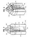
- FIG. 5is a perspective side view of one embodiment of a microstimulator with a support element, according to the invention.
- FIG. 6is a perspective view from a different angle of the microstimulator of FIG. 5 ;
- FIG. 7is a schematic overview of components for a system for microstimulation of body tissues, according to the invention.
- the inventionis directed to implantable microstimulators with one or more external electrodes and methods of manufacturing and using the devices.
- the inventionis directed to implantable microstimulators with one or more external electrodes disposed on a film substrate and methods of manufacturing and using the devices.
- implantable microstimulatorshave been made using housing and electrodes often disposed at the end(s) of the housing. Examples of such microstimulators are found in U.S. Pat. Nos. 5,139,539; 5,239,540; 5,312,439; 6,051,017; 6,609,032; U.S. Patent Application Publication No. 2004/0059392, now U.S. Pat. No. 7,437,193 issued Oct. 14, 2008 and PCT Patent Applications Publication Nos. 98/37926; 98/43700; and 98/43701.
- An implantable microstimulatorcan include a housing with one or more electrodes on a film substrate that is disposed on the exterior surface of the housing. Conductive vias through the housing provide contact with contact pads disposed on the film substrate to couple the electrodes with an electronic subassembly disposed within the housing. A support structure can also be provided to apply pressure to the film substrate and maintain contact between the contact pads and conductive vias.
- electrodes on only one side of the implantable microstimulatorcan be selected to provide stimulation of the desired tissue. This may provide more efficient stimulation of the tissue when compared to an implantable microstimulator with electrodes disposed on more than one side of the microstimulator or electrodes which provide roughly 360° stimulation from a portion (e.g., the tip) of the microstimulator.
- FIGS. 1 and 2illustrate a portion 100 of one embodiment of an implantable microstimulator.
- the implantable microstimulatorincludes a housing 102 , a power source 120 , an electronics subassembly 122 , an optional antenna 124 , one or more conductors 127 extending from the electronics subassembly 122 to the conductive via(s) 104 , and one or more conductive vias 104 extending through the housing to couple the electronic subassembly to electrodes disposed on the exterior of the housing.
- Other embodiments of an implantable microstimulatormay include more or fewer components.
- the power source 120components of the electronics subassembly 122 , and/or the optional antenna 124 can be provided outside of the housing in a separate unit and coupled to the implantable microstimulator by a lead. Examples of such arrangements are described in U.S. patent application Ser. No. 11/056,762, incorporated herein by reference.
- FIG. 3illustrates a second portion 150 of the implantable microstimulator.
- This portionincludes a first substrate 152 , one or more electrodes 154 , one or more contact pads 156 , conductor(s) 158 coupling the electrode(s) 154 to the contact pad(s) 156 , and optionally a second substrate 160 disposed over the first substrate so that at least a portion of the conductors is disposed between the first and second substrates.
- FIG. 4illustrates the two portions 100 , 150 ( FIGS. 2 and 3 ) coupled together with the contact pads 156 disposed over the vias 104 ( FIG. 1 ) so that the electrode(s) 154 are coupled to the electronic subassembly 122 ( FIG. 2 ) within the housing 102 .
- the housing 102can be formed of any material that resists the transport of moisture into the interior of the housing and is sufficiently sturdy to protect the components on the interior of the housing from damage under expected implantation and usage conditions. At least the portion of the housing 102 adjacent to the vias 104 is non-conductive. In some embodiments, the housing is entirely non-conductive. Suitable materials for the housing (or a portion of the housing) include metals, ceramics, and plastics.
- the housingcan have any shape including, for example, cylindrical, parallelepiped, cubic, and the like.
- a non-cylindrical shapefor example, a parallelepiped shape
- the non-cylindrical shapecan aid a practitioner in positioning the microstimulator correctly in relation to the tissue to be stimulated.
- the shapehas sides which are distinguishable based on at least one dimension.
- the housing 102has a roughly parallelepiped shape with two opposing sides 170 that are wider than two adjacent sides 172 . This difference in dimension can aid the practitioner implanting the device in correctly positioning the microstimulator relative to the tissue to be stimulated.
- the electrodes 154can be disposed on the wider side(s) 170 so that the practitioner can identify which side (for example, one of the wider sides) should be positioned adjacent the tissue to be stimulated.
- electrodesare provided on both of the wider sides of the housing so that a practitioner does not need to identify which of the two sides has electrodes. This can facilitate quicker implantation of the device into the patient.
- the lateral width of a side of the housingcan be the same or can vary along the length of the housing.
- the width of a sidecan be, for example, no greater then 5 mm, no greater than 4 mm, no greater than 3.3 mm, or no greater than 3 mm. This width can be in the range of from, for example, 1 to 5 mm.
- the length of the microstimulatoris no greater than 30 mm. Typically the length of the microstimulator is in the range of 10 to 30 mm.
- the housingcan be covered, in full or in part, with a coating.
- the coatingcan be provided to improve or alter one or more properties of the housing including, for example, biocompatibility, hydrophobicity, moisture permeability, leaching of material into or out of the housing, and the like.
- the optional coatingcan be a polymer material, inorganic material, or organic material.
- the housingmay be coated with an inorganic material, such as, for example, silicon dioxide, silicon nitride, titanium dioxide, or the like, to reduce moisture permeability.
- a silicone coatingmay be used to improve biocompatibility.
- a coatingcan be applied which contains a compound, such as, for example, a drug, prodrug, hormone, or other bioactive molecule, that can be released over time when the microstimulator is implanted.
- a plastic housingmay include such a compound to be released over time after implantation.
- the coatingincludes two or more layers of the same or different materials.
- the formation of the coatingcan be accomplished using any method including, for example, dip-coating, sputtering, reactive sputtering, physical or chemical vapor deposition, spray coating, and the like.
- the coatingcan be applied before the other microstimulator components have been assembled with the housing or at any other point in the microstimulator manufacturing process including applying the coating after the microstimulator has been completely assembled.
- the coatingis non-conductive.
- the one or more conductive vias 104are provided through a non-conductive portion of the housing 102 . In at least some embodiments, there are at least two conductive vias, but there can be any number of vias including two, four, six, eight, ten, or more conductive vias.
- the conductive vias 104can all be formed through a single side of the housing 102 , as illustrated in FIGS. 1 and 2 or vias can be formed through two or more sides of the housing.
- the vias 104are typically filled with a conductive material such as a metal (including alloys).
- the vias 104are used to couple the electrodes 154 to the electronic subassembly 122 which provides the stimulation signals to the electrodes.
- each viaincludes a channel 130 through the housing, a capture pad 132 disposed on the surface of the housing 102 , and an optional protrusion 134 ( FIG. 1 ) that can facilitate alignment and contact with the contact pads 156 .
- capture padscan also be formed on the interior surface of the housing to facilitate connection of the conductors 127 to the vias 104 .
- a non-conductive platee.g., a ceramic plate
- the holescan be provided in the plate by molding them in the plate or drilling the plate. The holes are filled with metal or other conductive material to form the channels of the via.
- a platinum (or other metal) pastecan be disposed in holes of a green state ceramic plate and then the plate and paste can be fired. In some instances, firing the ceramic plate may alter the position of the vias slightly. Providing the wider capture pads 132 over the vias 104 can reduce tolerances for registration of the contact pads 156 with the vias to maintain good electrical contact.
- a metal layercan be disposed on a surface of the plate and then the metal layer can be patterned using conventional techniques to form the capture pads 132 and optional protrusions 134 .
- a metal layercan be sputtered, or otherwise deposited using methods such as physical vapor deposition, chemical vapor deposition, electroplating, and electroless plating, onto the surface of the plate.
- the metal layercan be selectively etched to form the capture pads. Using capture pads that are larger in diameter than the vias can make connection with the contact pads easier and less sensitive to alignment.
- the first substrate 152can be a thin film substrate.
- the first substratecan be made of any suitable non-conductive material including polymers/plastics.
- the selected materialshould be suitable for the formation of electrodes, contact pads, and conductors on the material and it should be biocompatible.
- a suitable materialis polyimide.
- the contact pads 156 , conductors, 158 , and electrodes 154can be disposed on the first substrate 152 in any manner.
- a metal layercan be disposed on the first substrate 152 and the contact pads 156 , conductors, 158 , and electrodes 154 can be formed by etching the metal layer. Any deposition technique can be used to form the metal layer including physical vapor deposition, chemical vapor deposition, sputtering, and the like. Conventional etching techniques can be used to form the desired structures.
- the contact pads 156 , conductors, 158 , and electrodes 154can be formed by printing these components onto the substrate 152 using a conductive ink.
- a portion of the first substrate underneath the contact pads 156can be removed (for example, by etching) to expose the contact pads 156 to allow them to make contact with the capture pads 132 on the housing 102 .
- the contact padscan be formed on a side of the first substrate opposite the conductors and electrodes and vias can be formed through the first substrate and filled with conductive material to couple the contact pads to the conductors.
- the first substrate 152can have a variety of shapes and configurations.
- the substratecan be formed so that it can be disposed on two or more sides of the housing 102 or on a single side of the housing. In the illustrated example, the substrate is disposed on three sides of the housing. In some embodiments (such as the illustrated example), a substrate shape is selected so that electrodes can be disposed on two or more sides of the housing. In the illustrated example, electrodes are disposed on opposing sides of the housing. In other embodiments, electrodes may only be disposed on one side of the housing.
- the first substrate 152is attached to the housing 102 so that the first substrate does not move relative to the housing.
- the first substratecan be adhesively mounted onto the housing.
- a second substrate 160is disposed over at least a portion of the contact pads 156 and/or conductors 158 .
- the second substratecan be a single piece of material or can be several separate pieces.
- the second substrate 160leaves at least a portion of the electrodes 154 exposed.
- the second substrate 160can be selectively etched or die cut to expose the electrodes.
- the second substratecan be made of the same or a different material than the first substrate.
- the second substratecan be coupled to the first substrate using any method, including welding at least a portion of the first and second substrates together (e.g., around the periphery of the substrates) or adhesively mounting the second substrate on the first substrate.
- the second substrate 160can provide protection for the conductors 158 and/or contact pads 156 .
- the second substratecan provide support for the contact pads when a portion of the first substrate is removed to expose the contact pads to permit contact with the capture pads 132 .
- the electrodes 154typically form the anode and cathode of the microstimulator.
- the electronic subassemblymay be configured to allow each individual electrode to selectably operate as an anode or cathode or some electrodes may be designated as operable as cathodes only and other electrodes designated as operable as anodes only.
- the electronic subassemblymay be configured to allow multiple anodes and/or cathodes or may be configured to allow only one electrode to be an anode and one electrode to be a cathode at any given time.
- the electrodes 154 , conductors 158 , and contact pads 156can be formed using any conductive material. Examples of suitable materials include metals, alloys, conductive polymers/plastics, and conductive carbon.
- the microstimulatorincludes a support member 180 , as illustrated in FIGS. 5 and 6 , to facilitate and maintain contact between the contact pads 156 on the first substrate 152 and the capture pads 132 /vias 104 on the housing 102 .
- the support memberapplies pressure to maintain the contact.
- the support member 180includes a bridge 182 and a contact element 184 .
- the bridge 182is provided to attach the support member 180 to the housing 102 and hold the contact element 184 in place.
- a bridgecan be made of metal and can be welded to a metallic portion of the housing.
- a metallic ring 190can be brazed to a ceramic portion 192 of the housing 102 which contains the vias 104 .
- the metallic bridge 182is welded or otherwise attached to the metallic ring 190 .
- the contact element 184is disposed between the bridge 182 and the housing 102 .
- the contact element 184is formed of a non-conductive material.
- the material of the contact element 184is resilient and somewhat compressible. Such an arrangement may permit easier assembly as the resilient material can be slightly deformed to allow conformation of the contact element with the contact pads/capture pads.
- silicone rubbersuch as SILASTICTM.
- a power source 120can be disposed within the housing 100 .
- Any power sourcecan be used including, for example, a battery such as a primary battery or a rechargeable battery.
- Example of other power sourcesinclude super capacitors, nuclear or atomic batteries, mechanical resonators, infrared collectors, thermally-powered energy sources, flexural powered energy sources, bioenergy power sources, fuel cells, bioelectric cells, osmotic pressure pumps, and the like including the power sources described in U.S. Patent Application Publication No. 2004/0059392, now U.S. Pat. No. 7,437,193, incorporated herein by reference.
- powercan be supplied by an external power source through inductive coupling via the optional antenna 124 or a secondary antenna.
- the external power sourcecan be in a device that is mounted on the skin of the user or in a unit that is provided near the microstimulator user on a permanent or periodic basis.
- the batterymay be recharged using the optional antenna 124 , if desired. Power can be provided to the battery 120 for recharging by inductively coupling the battery through the antenna to a recharging unit 210 (see FIG. 7 ) external to the user. Examples of such arrangements can be found in the microstimulator references identified above.
- electrical currentis emitted by the electrodes 154 to stimulate motor nerve fibers, muscle fibers, or other body tissues near the microstimulator.
- the electronic subassembly 122provides the electronics used to operate the microstimulator and generate the electrical pulses at the electrodes 154 to produce stimulation of the body tissues.
- FIG. 7illustrates one embodiment of components of the electronic subassembly and associated units. It will be understood that the electronic subassembly can include more, fewer, or different components and can have a variety of different configurations including those configurations disclosed in the microstimulator references cited above. Some or all of the components of the electronic subassembly can be positioned on one or more circuit boards or similar carriers within the housing, if desired.
- a processor 204is provided to control the timing and electrical characteristics of the microstimulator.
- the processorcan, if desired, control one or more of the timing, frequency, strength, duration, and waveform of the pulses.
- the processor 204can select which electrodes can be used to provide stimulation, if desired.
- the processormay select which electrode(s) are cathodes and which electrode(s) are anodes.
- the processormay be used to identify which electrodes provide the most useful stimulation of the desired tissue. This process may be performed using an external programming unit, as described below, that is in communication with the processor 204 .
- any processorcan be used and can be as simple as an electronic device that produces pulses at a regular interval or the processor can be capable of receiving and interpreting instructions from an external programming unit 208 that allow modification of pulse characteristics.
- the processor 204is coupled to a receiver 202 which, in turn, is coupled to the optional antenna 124 . This allows the processor to receive instructions from an external source to direct the pulse characteristics and the selection of electrodes, if desired.
- the antenna 124is capable of receiving signals (e.g., RF signals) from an external telemetry unit 206 which is programmed by a programming unit 208 .
- the programming unit 208can be external to, or part of, the telemetry unit 206 .
- the telemetry unit 206can be a device that is worn on the skin of the user or can be carried by the user and can have a form similar to a pager or cellular phone, if desired.
- the telemetry unitmay not be worn or carried by the user but may only be available at a home station or at a clinician's office.
- the programming unit 208can be any unit that can provide information to the telemetry unit for transmission to the implanted microstimulator.
- the programming unit 208can be part of the telemetry unit 206 or can provide signals or information to the telemetry unit via a wireless or wired connection.
- One example of a suitable programming unitis a computer operated by the user or clinician to send signals to the telemetry unit.
- the signals sent to the processor 204 via the antenna 124 and receiver 202can be used to modify or otherwise direct the operation of the microstimulator.
- the signalsmay be used to modify the pulses of the microstimulator such as modifying one or more of pulse duration, pulse frequency, pulse waveform, and pulse strength.
- the signalsmay also direct the microstimulator to cease operation or to start operation or to start charging the battery.
- the microstimulatormay include a transmitter (not shown) coupled to the processor and antenna for transmitting signals back to the telemetry unit 206 or another unit capable of receiving the signals.
- the microstimulatormay transmit signals indicating whether the microstimulator is operating properly or not or indicating when the battery needs to be charged.
- the processormay also be capable of transmitting information about the pulse characteristics so that a user or clinician can determine or verify the characteristics.
- the optional antenna 124can have any form.
- the antennacomprises a coiled wire that is wrapped at least partially around the electronic subassembly within or on the housing.
- the electronic subassembly, power source, and antennacan be manufactured as described in U.S. Patent Application No. 2004/0059392, now U.S. Pat. No. 7,437,193. These components can then be placed inside the housing (or, alternatively, the housing can be formed, e.g., molded, around the components).
- the portion 150 of the microstimulator containing the film substrate 152 and electrodes 154 , as well as the vias 104 in the housing 102can be formed as described above. Coatings on the electrodes or housing, if any, can be applied at appropriate points during the manufacturing process.
Landscapes
- Health & Medical Sciences (AREA)
- Engineering & Computer Science (AREA)
- Biomedical Technology (AREA)
- Nuclear Medicine, Radiotherapy & Molecular Imaging (AREA)
- Radiology & Medical Imaging (AREA)
- Life Sciences & Earth Sciences (AREA)
- Animal Behavior & Ethology (AREA)
- General Health & Medical Sciences (AREA)
- Public Health (AREA)
- Veterinary Medicine (AREA)
- Neurology (AREA)
- Neurosurgery (AREA)
- Electrotherapy Devices (AREA)
Abstract
Description
Claims (20)
Priority Applications (1)
| Application Number | Priority Date | Filing Date | Title |
|---|---|---|---|
| US11/142,154US7957805B2 (en) | 2005-06-01 | 2005-06-01 | Implantable microstimulator with external electrodes disposed on a film substrate and methods of manufacture and use |
Applications Claiming Priority (1)
| Application Number | Priority Date | Filing Date | Title |
|---|---|---|---|
| US11/142,154US7957805B2 (en) | 2005-06-01 | 2005-06-01 | Implantable microstimulator with external electrodes disposed on a film substrate and methods of manufacture and use |
Publications (2)
| Publication Number | Publication Date |
|---|---|
| US20060276842A1 US20060276842A1 (en) | 2006-12-07 |
| US7957805B2true US7957805B2 (en) | 2011-06-07 |
Family
ID=37495142
Family Applications (1)
| Application Number | Title | Priority Date | Filing Date |
|---|---|---|---|
| US11/142,154Expired - Fee RelatedUS7957805B2 (en) | 2005-06-01 | 2005-06-01 | Implantable microstimulator with external electrodes disposed on a film substrate and methods of manufacture and use |
Country Status (1)
| Country | Link |
|---|---|
| US (1) | US7957805B2 (en) |
Cited By (13)
| Publication number | Priority date | Publication date | Assignee | Title |
|---|---|---|---|---|
| WO2015095233A1 (en) | 2013-12-19 | 2015-06-25 | Boston Scientific Neuromodulation Corporation | Methods and systems for employing a duty cycle in electrical stimulation of patient tissue |
| US9072904B2 (en) | 2006-10-18 | 2015-07-07 | Boston Scientific Neuromodulation Corporation | Multi-electrode implantable stimulator device with a single current path decoupling capacitor |
| US9289612B1 (en) | 2014-12-11 | 2016-03-22 | Medtronic Inc. | Coordination of ventricular pacing in a leadless pacing system |
| US9399140B2 (en) | 2014-07-25 | 2016-07-26 | Medtronic, Inc. | Atrial contraction detection by a ventricular leadless pacing device for atrio-synchronous ventricular pacing |
| US9492669B2 (en) | 2014-11-11 | 2016-11-15 | Medtronic, Inc. | Mode switching by a ventricular leadless pacing device |
| US9492668B2 (en) | 2014-11-11 | 2016-11-15 | Medtronic, Inc. | Mode switching by a ventricular leadless pacing device |
| US9623234B2 (en) | 2014-11-11 | 2017-04-18 | Medtronic, Inc. | Leadless pacing device implantation |
| US9724519B2 (en) | 2014-11-11 | 2017-08-08 | Medtronic, Inc. | Ventricular leadless pacing device mode switching |
| US10390720B2 (en) | 2014-07-17 | 2019-08-27 | Medtronic, Inc. | Leadless pacing system including sensing extension |
| US11207527B2 (en) | 2016-07-06 | 2021-12-28 | Cardiac Pacemakers, Inc. | Method and system for determining an atrial contraction timing fiducial in a leadless cardiac pacemaker system |
| US11617879B2 (en)* | 2012-12-07 | 2023-04-04 | Medtronic, Inc. | Minimally invasive implantable neurostimulation system |
| US12357792B2 (en) | 2019-01-04 | 2025-07-15 | Shifamed Holdings, Llc | Internal recharging systems and methods of use |
| US12440656B2 (en) | 2021-04-23 | 2025-10-14 | Shifamed Holdings, Llc | Power management for interatrial shunts and associated systems and methods |
Families Citing this family (6)
| Publication number | Priority date | Publication date | Assignee | Title |
|---|---|---|---|---|
| US7920915B2 (en)* | 2005-11-16 | 2011-04-05 | Boston Scientific Neuromodulation Corporation | Implantable stimulator |
| WO2007098200A2 (en)* | 2006-02-16 | 2007-08-30 | Imthera Medical, Inc. | An rfid-based apparatus, system, and method for therapeutic treatment of obstructive sleep apnea |
| WO2008157435A1 (en)* | 2007-06-14 | 2008-12-24 | Northstar Neuroscience, Nc. | Microdevice-based electrode assemblies and associated neural stimulation systems, devices, and methods |
| US8131377B2 (en)* | 2007-07-11 | 2012-03-06 | Boston Scientific Neuromodulation Corporation | Telemetry listening window management for an implantable medical device |
| EP2395839B1 (en)* | 2009-02-13 | 2014-05-07 | Topica Pharmaceuticals, Inc | Anti-fungal formulation |
| WO2021163489A1 (en)* | 2020-02-13 | 2021-08-19 | Cardiac Pacemakers, Inc. | Implantable medical device having a biocompatible circuit board with embedded electrodes |
Citations (29)
| Publication number | Priority date | Publication date | Assignee | Title |
|---|---|---|---|---|
| US3718142A (en) | 1971-04-23 | 1973-02-27 | Medtronic Inc | Electrically shielded, gas-permeable implantable electro-medical apparatus |
| US3926198A (en)* | 1974-06-10 | 1975-12-16 | Arco Med Prod Co | Cardiac pacer |
| US4254775A (en)* | 1979-07-02 | 1981-03-10 | Mieczyslaw Mirowski | Implantable defibrillator and package therefor |
| US5103818A (en)* | 1990-11-13 | 1992-04-14 | Siemens-Pacesetter, Inc. | System and method for completing electrical connections in an implantable medical device |
| US5193539A (en) | 1991-12-18 | 1993-03-16 | Alfred E. Mann Foundation For Scientific Research | Implantable microstimulator |
| US5193540A (en) | 1991-12-18 | 1993-03-16 | Alfred E. Mann Foundation For Scientific Research | Structure and method of manufacture of an implantable microstimulator |
| EP0534782A1 (en)* | 1991-09-26 | 1993-03-31 | Medtronic, Inc. | Implantable medical device enclosure |
| US5207218A (en)* | 1991-02-27 | 1993-05-04 | Medtronic, Inc. | Implantable pulse generator |
| US5312439A (en) | 1991-12-12 | 1994-05-17 | Loeb Gerald E | Implantable device having an electrolytic storage electrode |
| US5314458A (en)* | 1990-06-01 | 1994-05-24 | University Of Michigan | Single channel microstimulator |
| US5535097A (en)* | 1993-11-23 | 1996-07-09 | Medtronic, Inc. | Implantable medical device including a first enclosure portion having a feedthrough in a second interior surface |
| US5607463A (en)* | 1993-03-30 | 1997-03-04 | Medtronic, Inc. | Intravascular medical device |
| US5645572A (en)* | 1996-03-12 | 1997-07-08 | Angeion Corporation | Implantable cardioverter defibrillator with slew rate limiting |
| US5755743A (en)* | 1996-06-05 | 1998-05-26 | Implex Gmbh Spezialhorgerate | Implantable unit |
| WO1998037926A1 (en) | 1997-02-26 | 1998-09-03 | Alfred E. Mann Foundation For Scientific Research | Battery-powered patient implantable device |
| US5817130A (en)* | 1996-05-03 | 1998-10-06 | Sulzer Intermedics Inc. | Implantable cardiac cardioverter/defibrillator with EMI suppression filter with independent ground connection |
| WO1998043700A1 (en) | 1997-03-27 | 1998-10-08 | Alfred E. Mann Foundation For Scientific Research | System of implantable devices for monitoring and/or affecting body parameters |
| US5895980A (en)* | 1996-12-30 | 1999-04-20 | Medical Pacing Concepts, Ltd. | Shielded pacemaker enclosure |
| US6051017A (en)* | 1996-02-20 | 2000-04-18 | Advanced Bionics Corporation | Implantable microstimulator and systems employing the same |
| US6315721B2 (en)* | 1997-02-26 | 2001-11-13 | Alfred E. Mann Foundation For Scientific Research | System of implantable devices for monitoring and/or affecting body parameters |
| US6453199B1 (en)* | 1996-04-01 | 2002-09-17 | Valery Ivanovich Kobozev | Electrical gastro-intestinal tract stimulator |
| US20020171065A1 (en)* | 2001-04-02 | 2002-11-21 | Nashua Corporation | Circuit elements having an embedded conductive trace and methods of manufacture |
| US20030097166A1 (en)* | 2001-11-16 | 2003-05-22 | The Regents Of The University Of California | Flexible electrode array for artifical vision |
| US6609032B1 (en) | 1999-01-07 | 2003-08-19 | Advanced Bionics Corporation | Fitting process for a neural stimulation system |
| US20040059392A1 (en)* | 2002-06-28 | 2004-03-25 | Jordi Parramon | Microstimulator having self-contained power source |
| US20040068298A1 (en)* | 2000-03-17 | 2004-04-08 | Jordi Parramon | Voltage converter for implantable microstimulator using RF-powering coil |
| US20040260372A1 (en)* | 2003-06-23 | 2004-12-23 | Canfield David L. | Housing for an implantable medical device |
| US7047074B2 (en)* | 2001-02-20 | 2006-05-16 | Biophan Technologies, Inc. | Electromagnetic interference immune tissue invasive system |
| US20060212075A1 (en)* | 2005-03-18 | 2006-09-21 | Marnfeldt Goran N | Implantable microstimulator with conductive plastic electrode and methods of manufacture and use |
Family Cites Families (1)
| Publication number | Priority date | Publication date | Assignee | Title |
|---|---|---|---|---|
| US3718412A (en)* | 1971-10-01 | 1973-02-27 | Ramsey Corp | Pumping seal for rotary piston engines |
- 2005
- 2005-06-01USUS11/142,154patent/US7957805B2/ennot_activeExpired - Fee Related
Patent Citations (30)
| Publication number | Priority date | Publication date | Assignee | Title |
|---|---|---|---|---|
| US3718142A (en) | 1971-04-23 | 1973-02-27 | Medtronic Inc | Electrically shielded, gas-permeable implantable electro-medical apparatus |
| US3926198A (en)* | 1974-06-10 | 1975-12-16 | Arco Med Prod Co | Cardiac pacer |
| US4254775A (en)* | 1979-07-02 | 1981-03-10 | Mieczyslaw Mirowski | Implantable defibrillator and package therefor |
| US5314458A (en)* | 1990-06-01 | 1994-05-24 | University Of Michigan | Single channel microstimulator |
| US5103818A (en)* | 1990-11-13 | 1992-04-14 | Siemens-Pacesetter, Inc. | System and method for completing electrical connections in an implantable medical device |
| US5207218A (en)* | 1991-02-27 | 1993-05-04 | Medtronic, Inc. | Implantable pulse generator |
| EP0534782A1 (en)* | 1991-09-26 | 1993-03-31 | Medtronic, Inc. | Implantable medical device enclosure |
| US5312439A (en) | 1991-12-12 | 1994-05-17 | Loeb Gerald E | Implantable device having an electrolytic storage electrode |
| US5193540A (en) | 1991-12-18 | 1993-03-16 | Alfred E. Mann Foundation For Scientific Research | Structure and method of manufacture of an implantable microstimulator |
| US5193539A (en) | 1991-12-18 | 1993-03-16 | Alfred E. Mann Foundation For Scientific Research | Implantable microstimulator |
| US5607463A (en)* | 1993-03-30 | 1997-03-04 | Medtronic, Inc. | Intravascular medical device |
| US5535097A (en)* | 1993-11-23 | 1996-07-09 | Medtronic, Inc. | Implantable medical device including a first enclosure portion having a feedthrough in a second interior surface |
| US6051017A (en)* | 1996-02-20 | 2000-04-18 | Advanced Bionics Corporation | Implantable microstimulator and systems employing the same |
| US5645572A (en)* | 1996-03-12 | 1997-07-08 | Angeion Corporation | Implantable cardioverter defibrillator with slew rate limiting |
| US6453199B1 (en)* | 1996-04-01 | 2002-09-17 | Valery Ivanovich Kobozev | Electrical gastro-intestinal tract stimulator |
| US5817130A (en)* | 1996-05-03 | 1998-10-06 | Sulzer Intermedics Inc. | Implantable cardiac cardioverter/defibrillator with EMI suppression filter with independent ground connection |
| US5755743A (en)* | 1996-06-05 | 1998-05-26 | Implex Gmbh Spezialhorgerate | Implantable unit |
| US5895980A (en)* | 1996-12-30 | 1999-04-20 | Medical Pacing Concepts, Ltd. | Shielded pacemaker enclosure |
| WO1998037926A1 (en) | 1997-02-26 | 1998-09-03 | Alfred E. Mann Foundation For Scientific Research | Battery-powered patient implantable device |
| US6315721B2 (en)* | 1997-02-26 | 2001-11-13 | Alfred E. Mann Foundation For Scientific Research | System of implantable devices for monitoring and/or affecting body parameters |
| WO1998043701A1 (en) | 1997-03-27 | 1998-10-08 | Alfred E. Mann Foundation For Scientific Research | System of implantable devices for monitoring and/or affecting body parameters |
| WO1998043700A1 (en) | 1997-03-27 | 1998-10-08 | Alfred E. Mann Foundation For Scientific Research | System of implantable devices for monitoring and/or affecting body parameters |
| US6609032B1 (en) | 1999-01-07 | 2003-08-19 | Advanced Bionics Corporation | Fitting process for a neural stimulation system |
| US20040068298A1 (en)* | 2000-03-17 | 2004-04-08 | Jordi Parramon | Voltage converter for implantable microstimulator using RF-powering coil |
| US7047074B2 (en)* | 2001-02-20 | 2006-05-16 | Biophan Technologies, Inc. | Electromagnetic interference immune tissue invasive system |
| US20020171065A1 (en)* | 2001-04-02 | 2002-11-21 | Nashua Corporation | Circuit elements having an embedded conductive trace and methods of manufacture |
| US20030097166A1 (en)* | 2001-11-16 | 2003-05-22 | The Regents Of The University Of California | Flexible electrode array for artifical vision |
| US20040059392A1 (en)* | 2002-06-28 | 2004-03-25 | Jordi Parramon | Microstimulator having self-contained power source |
| US20040260372A1 (en)* | 2003-06-23 | 2004-12-23 | Canfield David L. | Housing for an implantable medical device |
| US20060212075A1 (en)* | 2005-03-18 | 2006-09-21 | Marnfeldt Goran N | Implantable microstimulator with conductive plastic electrode and methods of manufacture and use |
Non-Patent Citations (2)
| Title |
|---|
| U.S. Appl. No. 11/040,209, filed Jan. 20, 2005, Inventor Colvin et al., "Implantable Microstimulator with Plastic Housing and Methods of Manufacture and Use". |
| U.S. Appl. No. 11/056,762, filed Feb. 11, 2005, Inventor He, "An Implantable Microstimulator Having a Separate Battery Unit and Methods of Use Thereof". |
Cited By (22)
| Publication number | Priority date | Publication date | Assignee | Title |
|---|---|---|---|---|
| US9072904B2 (en) | 2006-10-18 | 2015-07-07 | Boston Scientific Neuromodulation Corporation | Multi-electrode implantable stimulator device with a single current path decoupling capacitor |
| US11364378B2 (en) | 2006-10-18 | 2022-06-21 | Boston Scientific Neuromodulation Corporation | Multi-electrode implantable stimulator device with a single current path decoupling capacitor |
| US9737713B2 (en) | 2006-10-18 | 2017-08-22 | Boston Scientific Neuromodulation Corporation | Multi-electrode implantable stimulator device with a single current path decoupling capacitor |
| US10518091B2 (en) | 2006-10-18 | 2019-12-31 | Boston Scientific Neuromodulation Corporation | Multi-electrode implantable stimulator device with a single current path decoupling capacitor |
| US11617879B2 (en)* | 2012-12-07 | 2023-04-04 | Medtronic, Inc. | Minimally invasive implantable neurostimulation system |
| WO2015095233A1 (en) | 2013-12-19 | 2015-06-25 | Boston Scientific Neuromodulation Corporation | Methods and systems for employing a duty cycle in electrical stimulation of patient tissue |
| EP4000680A2 (en) | 2013-12-19 | 2022-05-25 | Boston Scientific Neuromodulation Corporation | Methods and systems for employing a duty cycle in electrical stimulation of patient tissue |
| US9643010B2 (en) | 2013-12-19 | 2017-05-09 | Boston Scientific Neuromodulation Corporation | Methods and systems for employing a duty cycle in electrical stimulation of patient tissue |
| US10390720B2 (en) | 2014-07-17 | 2019-08-27 | Medtronic, Inc. | Leadless pacing system including sensing extension |
| US10674928B2 (en) | 2014-07-17 | 2020-06-09 | Medtronic, Inc. | Leadless pacing system including sensing extension |
| US9399140B2 (en) | 2014-07-25 | 2016-07-26 | Medtronic, Inc. | Atrial contraction detection by a ventricular leadless pacing device for atrio-synchronous ventricular pacing |
| USRE48197E1 (en) | 2014-07-25 | 2020-09-08 | Medtronic, Inc. | Atrial contraction detection by a ventricular leadless pacing device for atrio-synchronous ventricular pacing |
| US9492668B2 (en) | 2014-11-11 | 2016-11-15 | Medtronic, Inc. | Mode switching by a ventricular leadless pacing device |
| US10279168B2 (en) | 2014-11-11 | 2019-05-07 | Medtronic, Inc. | Leadless pacing device implantation |
| US9808628B2 (en) | 2014-11-11 | 2017-11-07 | Medtronic, Inc. | Mode switching by a ventricular leadless pacing device |
| US9724519B2 (en) | 2014-11-11 | 2017-08-08 | Medtronic, Inc. | Ventricular leadless pacing device mode switching |
| US9623234B2 (en) | 2014-11-11 | 2017-04-18 | Medtronic, Inc. | Leadless pacing device implantation |
| US9492669B2 (en) | 2014-11-11 | 2016-11-15 | Medtronic, Inc. | Mode switching by a ventricular leadless pacing device |
| US9289612B1 (en) | 2014-12-11 | 2016-03-22 | Medtronic Inc. | Coordination of ventricular pacing in a leadless pacing system |
| US11207527B2 (en) | 2016-07-06 | 2021-12-28 | Cardiac Pacemakers, Inc. | Method and system for determining an atrial contraction timing fiducial in a leadless cardiac pacemaker system |
| US12357792B2 (en) | 2019-01-04 | 2025-07-15 | Shifamed Holdings, Llc | Internal recharging systems and methods of use |
| US12440656B2 (en) | 2021-04-23 | 2025-10-14 | Shifamed Holdings, Llc | Power management for interatrial shunts and associated systems and methods |
Also Published As
| Publication number | Publication date |
|---|---|
| US20060276842A1 (en) | 2006-12-07 |
Similar Documents
| Publication | Publication Date | Title |
|---|---|---|
| US8060215B2 (en) | Implantable microstimulator having a battery unit and methods of use therefor | |
| US7957805B2 (en) | Implantable microstimulator with external electrodes disposed on a film substrate and methods of manufacture and use | |
| US20070219595A1 (en) | Stimulator system with electrode array and the method of making the same | |
| US7330756B2 (en) | Implantable microstimulator with conductive plastic electrode and methods of manufacture and use | |
| US7672734B2 (en) | Non-linear electrode array | |
| US7706892B2 (en) | Implantable microstimulator with plastic housing and methods of manufacture and use | |
| US8700178B2 (en) | Stimulator leads and methods for lead fabrication | |
| US9744367B2 (en) | Feed through interconnect assembly for an implantable stimulation system and methods of making and using | |
| US20100262201A1 (en) | Implantable stimulator with integrated plastic housing/metal contacts and manufacture and use | |
| US7444180B2 (en) | Implantable microstimulator with dissecting tip and/or retrieving anchor and methods of manufacture and use | |
| US8712542B2 (en) | Deposited conductive layers for leads of implantable electric stimulation systems and methods of making and using | |
| US8359107B2 (en) | Electrode design for leads of implantable electric stimulation systems and methods of making and using | |
| US8406883B1 (en) | Lead assembly for electrical stimulation systems and methods of making and using | |
| US20080140168A1 (en) | Electrode arrangements for tissue stimulation and methods of use and manufacture | |
| US9351655B2 (en) | Systems, devices, and methods for electrically coupling terminals to electrodes of electrical stimulation systems | |
| AU2007235178B2 (en) | Non-linear electrode array | |
| US8249721B2 (en) | Method for fabricating a neurostimulation lead contact array | |
| US20220226641A1 (en) | Electrical stimulation cuff devices and systems with directional electrode configurations |
Legal Events
| Date | Code | Title | Description |
|---|---|---|---|
| AS | Assignment | Owner name:ADVANCED BIONICS CORPORATION, CALIFORNIA Free format text:ASSIGNMENT OF ASSIGNORS INTEREST;ASSIGNOR:HE, TOM XIAOHAI;REEL/FRAME:018519/0036 Effective date:20050527 | |
| AS | Assignment | Owner name:BOSTON SCIENTIFIC NEUROMODULATION CORPORATION, CAL Free format text:CHANGE OF NAME;ASSIGNOR:ADVANCED BIONICS CORPORATION;REEL/FRAME:020296/0477 Effective date:20071116 Owner name:BOSTON SCIENTIFIC NEUROMODULATION CORPORATION, CALIFORNIA Free format text:CHANGE OF NAME;ASSIGNOR:ADVANCED BIONICS CORPORATION;REEL/FRAME:020296/0477 Effective date:20071116 Owner name:BOSTON SCIENTIFIC NEUROMODULATION CORPORATION,CALI Free format text:CHANGE OF NAME;ASSIGNOR:ADVANCED BIONICS CORPORATION;REEL/FRAME:020296/0477 Effective date:20071116 | |
| STCF | Information on status: patent grant | Free format text:PATENTED CASE | |
| FPAY | Fee payment | Year of fee payment:4 | |
| FEPP | Fee payment procedure | Free format text:MAINTENANCE FEE REMINDER MAILED (ORIGINAL EVENT CODE: REM.); ENTITY STATUS OF PATENT OWNER: LARGE ENTITY | |
| LAPS | Lapse for failure to pay maintenance fees | Free format text:PATENT EXPIRED FOR FAILURE TO PAY MAINTENANCE FEES (ORIGINAL EVENT CODE: EXP.); ENTITY STATUS OF PATENT OWNER: LARGE ENTITY | |
| STCH | Information on status: patent discontinuation | Free format text:PATENT EXPIRED DUE TO NONPAYMENT OF MAINTENANCE FEES UNDER 37 CFR 1.362 | |
| FP | Lapsed due to failure to pay maintenance fee | Effective date:20190607 |