US7956383B2 - Field effect transistor - Google Patents
Field effect transistorDownload PDFInfo
- Publication number
- US7956383B2 US7956383B2US12/060,505US6050508AUS7956383B2US 7956383 B2US7956383 B2US 7956383B2US 6050508 AUS6050508 AUS 6050508AUS 7956383 B2US7956383 B2US 7956383B2
- Authority
- US
- United States
- Prior art keywords
- nitride semiconductor
- plane
- semiconductor layer
- field effect
- effect transistor
- Prior art date
- Legal status (The legal status is an assumption and is not a legal conclusion. Google has not performed a legal analysis and makes no representation as to the accuracy of the status listed.)
- Active, expires
Links
- 230000005669field effectEffects0.000titleclaimsabstractdescription67
- 239000004065semiconductorSubstances0.000claimsabstractdescription78
- 150000004767nitridesChemical class0.000claimsabstractdescription71
- 239000010410layerSubstances0.000claimsdescription171
- 239000012535impuritySubstances0.000claimsdescription7
- 239000002356single layerSubstances0.000claimsdescription2
- 229910002601GaNInorganic materials0.000description75
- JMASRVWKEDWRBT-UHFFFAOYSA-NGallium nitrideChemical compound[Ga]#NJMASRVWKEDWRBT-UHFFFAOYSA-N0.000description75
- 229910002704AlGaNInorganic materials0.000description53
- 238000000034methodMethods0.000description37
- 230000004888barrier functionEffects0.000description24
- 229910052581Si3N4Inorganic materials0.000description23
- HQVNEWCFYHHQES-UHFFFAOYSA-Nsilicon nitrideChemical compoundN12[Si]34N5[Si]62N3[Si]51N64HQVNEWCFYHHQES-UHFFFAOYSA-N0.000description22
- 239000000758substrateSubstances0.000description20
- 238000002955isolationMethods0.000description13
- 229910052594sapphireInorganic materials0.000description13
- 239000010980sapphireSubstances0.000description13
- 238000004519manufacturing processMethods0.000description12
- VYPSYNLAJGMNEJ-UHFFFAOYSA-NSilicium dioxideChemical compoundO=[Si]=OVYPSYNLAJGMNEJ-UHFFFAOYSA-N0.000description10
- 230000015572biosynthetic processEffects0.000description9
- 230000000052comparative effectEffects0.000description9
- 230000004048modificationEffects0.000description9
- 238000012986modificationMethods0.000description9
- 230000010287polarizationEffects0.000description9
- PMHQVHHXPFUNSP-UHFFFAOYSA-Mcopper(1+);methylsulfanylmethane;bromideChemical compoundBr[Cu].CSCPMHQVHHXPFUNSP-UHFFFAOYSA-M0.000description7
- 238000012545processingMethods0.000description7
- 239000000969carrierSubstances0.000description6
- 238000001312dry etchingMethods0.000description6
- 230000000694effectsEffects0.000description6
- CJNBYAVZURUTKZ-UHFFFAOYSA-Nhafnium(IV) oxideInorganic materialsO=[Hf]=OCJNBYAVZURUTKZ-UHFFFAOYSA-N0.000description5
- 239000000377silicon dioxideSubstances0.000description5
- 230000015556catabolic processEffects0.000description4
- 230000008859changeEffects0.000description4
- 229910052681coesiteInorganic materials0.000description4
- 229910052906cristobaliteInorganic materials0.000description4
- 150000002500ionsChemical class0.000description4
- 229910052751metalInorganic materials0.000description4
- 239000002184metalSubstances0.000description4
- 238000005268plasma chemical vapour depositionMethods0.000description4
- 230000008569processEffects0.000description4
- 125000006850spacer groupChemical group0.000description4
- 230000002269spontaneous effectEffects0.000description4
- 238000004544sputter depositionMethods0.000description4
- 229910052682stishoviteInorganic materials0.000description4
- 239000010936titaniumSubstances0.000description4
- 229910052905tridymiteInorganic materials0.000description4
- ZOXJGFHDIHLPTG-UHFFFAOYSA-NBoronChemical compound[B]ZOXJGFHDIHLPTG-UHFFFAOYSA-N0.000description3
- KRHYYFGTRYWZRS-UHFFFAOYSA-NFluoraneChemical compoundFKRHYYFGTRYWZRS-UHFFFAOYSA-N0.000description3
- YCKRFDGAMUMZLT-UHFFFAOYSA-NFluorine atomChemical compound[F]YCKRFDGAMUMZLT-UHFFFAOYSA-N0.000description3
- 229910021140PdSiInorganic materials0.000description3
- PNEYBMLMFCGWSK-UHFFFAOYSA-Naluminium oxideInorganic materials[O-2].[O-2].[O-2].[Al+3].[Al+3]PNEYBMLMFCGWSK-UHFFFAOYSA-N0.000description3
- 229910052796boronInorganic materials0.000description3
- 229910052593corundumInorganic materials0.000description3
- 238000010586diagramMethods0.000description3
- 229910052731fluorineInorganic materials0.000description3
- 239000011737fluorineSubstances0.000description3
- 238000002513implantationMethods0.000description3
- 230000003647oxidationEffects0.000description3
- 238000007254oxidation reactionMethods0.000description3
- HBMJWWWQQXIZIP-UHFFFAOYSA-Nsilicon carbideChemical compound[Si+]#[C-]HBMJWWWQQXIZIP-UHFFFAOYSA-N0.000description3
- 229910001845yogo sapphireInorganic materials0.000description3
- IJGRMHOSHXDMSA-UHFFFAOYSA-NAtomic nitrogenChemical compoundN#NIJGRMHOSHXDMSA-UHFFFAOYSA-N0.000description2
- KDLHZDBZIXYQEI-UHFFFAOYSA-NPalladiumChemical compound[Pd]KDLHZDBZIXYQEI-UHFFFAOYSA-N0.000description2
- 229910007991Si-NInorganic materials0.000description2
- XUIMIQQOPSSXEZ-UHFFFAOYSA-NSiliconChemical compound[Si]XUIMIQQOPSSXEZ-UHFFFAOYSA-N0.000description2
- 229910006294Si—NInorganic materials0.000description2
- 238000005229chemical vapour depositionMethods0.000description2
- 238000009616inductively coupled plasmaMethods0.000description2
- 238000005468ion implantationMethods0.000description2
- 239000000463materialSubstances0.000description2
- 230000003071parasitic effectEffects0.000description2
- 229920006395saturated elastomerPolymers0.000description2
- 229910052710siliconInorganic materials0.000description2
- 239000010703siliconSubstances0.000description2
- 229910010271silicon carbideInorganic materials0.000description2
- 238000005245sinteringMethods0.000description2
- 238000012546transferMethods0.000description2
- RTAQQCXQSZGOHL-UHFFFAOYSA-NTitaniumChemical compound[Ti]RTAQQCXQSZGOHL-UHFFFAOYSA-N0.000description1
- AUCDRFABNLOFRE-UHFFFAOYSA-Nalumane;indiumChemical compound[AlH3].[In]AUCDRFABNLOFRE-UHFFFAOYSA-N0.000description1
- 229910052782aluminiumInorganic materials0.000description1
- XAGFODPZIPBFFR-UHFFFAOYSA-NaluminiumChemical compound[Al]XAGFODPZIPBFFR-UHFFFAOYSA-N0.000description1
- RNQKDQAVIXDKAG-UHFFFAOYSA-Naluminum galliumChemical compound[Al].[Ga]RNQKDQAVIXDKAG-UHFFFAOYSA-N0.000description1
- 150000001875compoundsChemical class0.000description1
- 239000013078crystalSubstances0.000description1
- 238000006731degradation reactionMethods0.000description1
- 238000005530etchingMethods0.000description1
- 238000002474experimental methodMethods0.000description1
- 239000003574free electronSubstances0.000description1
- 239000007789gasSubstances0.000description1
- 239000012212insulatorSubstances0.000description1
- QPJSUIGXIBEQAC-UHFFFAOYSA-Nn-(2,4-dichloro-5-propan-2-yloxyphenyl)acetamideChemical compoundCC(C)OC1=CC(NC(C)=O)=C(Cl)C=C1ClQPJSUIGXIBEQAC-UHFFFAOYSA-N0.000description1
- 229910052757nitrogenInorganic materials0.000description1
- TWNQGVIAIRXVLR-UHFFFAOYSA-Noxo(oxoalumanyloxy)alumaneChemical compoundO=[Al]O[Al]=OTWNQGVIAIRXVLR-UHFFFAOYSA-N0.000description1
- 229910052763palladiumInorganic materials0.000description1
- 230000000704physical effectEffects0.000description1
- 230000009467reductionEffects0.000description1
- 230000000630rising effectEffects0.000description1
- 235000012239silicon dioxideNutrition0.000description1
- 229910052719titaniumInorganic materials0.000description1
Images


Classifications
- H—ELECTRICITY
- H10—SEMICONDUCTOR DEVICES; ELECTRIC SOLID-STATE DEVICES NOT OTHERWISE PROVIDED FOR
- H10D—INORGANIC ELECTRIC SEMICONDUCTOR DEVICES
- H10D30/00—Field-effect transistors [FET]
- H10D30/40—FETs having zero-dimensional [0D], one-dimensional [1D] or two-dimensional [2D] charge carrier gas channels
- H10D30/47—FETs having zero-dimensional [0D], one-dimensional [1D] or two-dimensional [2D] charge carrier gas channels having 2D charge carrier gas channels, e.g. nanoribbon FETs or high electron mobility transistors [HEMT]
- H10D30/471—High electron mobility transistors [HEMT] or high hole mobility transistors [HHMT]
- H10D30/475—High electron mobility transistors [HEMT] or high hole mobility transistors [HHMT] having wider bandgap layer formed on top of lower bandgap active layer, e.g. undoped barrier HEMTs such as i-AlGaN/GaN HEMTs
- H10D30/4755—High electron mobility transistors [HEMT] or high hole mobility transistors [HHMT] having wider bandgap layer formed on top of lower bandgap active layer, e.g. undoped barrier HEMTs such as i-AlGaN/GaN HEMTs having wide bandgap charge-carrier supplying layers, e.g. modulation doped HEMTs such as n-AlGaAs/GaAs HEMTs
- H—ELECTRICITY
- H10—SEMICONDUCTOR DEVICES; ELECTRIC SOLID-STATE DEVICES NOT OTHERWISE PROVIDED FOR
- H10D—INORGANIC ELECTRIC SEMICONDUCTOR DEVICES
- H10D30/00—Field-effect transistors [FET]
- H10D30/01—Manufacture or treatment
- H10D30/015—Manufacture or treatment of FETs having heterojunction interface channels or heterojunction gate electrodes, e.g. HEMT
- H—ELECTRICITY
- H10—SEMICONDUCTOR DEVICES; ELECTRIC SOLID-STATE DEVICES NOT OTHERWISE PROVIDED FOR
- H10D—INORGANIC ELECTRIC SEMICONDUCTOR DEVICES
- H10D64/00—Electrodes of devices having potential barriers
- H10D64/20—Electrodes characterised by their shapes, relative sizes or dispositions
- H10D64/27—Electrodes not carrying the current to be rectified, amplified, oscillated or switched, e.g. gates
- H10D64/311—Gate electrodes for field-effect devices
- H10D64/411—Gate electrodes for field-effect devices for FETs
- H10D64/511—Gate electrodes for field-effect devices for FETs for IGFETs
- H10D64/517—Gate electrodes for field-effect devices for FETs for IGFETs characterised by the conducting layers
- H10D64/518—Gate electrodes for field-effect devices for FETs for IGFETs characterised by the conducting layers characterised by their lengths or sectional shapes
- H—ELECTRICITY
- H10—SEMICONDUCTOR DEVICES; ELECTRIC SOLID-STATE DEVICES NOT OTHERWISE PROVIDED FOR
- H10D—INORGANIC ELECTRIC SEMICONDUCTOR DEVICES
- H10D62/00—Semiconductor bodies, or regions thereof, of devices having potential barriers
- H10D62/40—Crystalline structures
- H10D62/405—Orientations of crystalline planes
- H—ELECTRICITY
- H10—SEMICONDUCTOR DEVICES; ELECTRIC SOLID-STATE DEVICES NOT OTHERWISE PROVIDED FOR
- H10D—INORGANIC ELECTRIC SEMICONDUCTOR DEVICES
- H10D62/00—Semiconductor bodies, or regions thereof, of devices having potential barriers
- H10D62/80—Semiconductor bodies, or regions thereof, of devices having potential barriers characterised by the materials
- H10D62/85—Semiconductor bodies, or regions thereof, of devices having potential barriers characterised by the materials being Group III-V materials, e.g. GaAs
- H10D62/8503—Nitride Group III-V materials, e.g. AlN or GaN
- H—ELECTRICITY
- H10—SEMICONDUCTOR DEVICES; ELECTRIC SOLID-STATE DEVICES NOT OTHERWISE PROVIDED FOR
- H10D—INORGANIC ELECTRIC SEMICONDUCTOR DEVICES
- H10D64/00—Electrodes of devices having potential barriers
- H10D64/20—Electrodes characterised by their shapes, relative sizes or dispositions
- H10D64/27—Electrodes not carrying the current to be rectified, amplified, oscillated or switched, e.g. gates
- H10D64/311—Gate electrodes for field-effect devices
- H10D64/411—Gate electrodes for field-effect devices for FETs
- H10D64/511—Gate electrodes for field-effect devices for FETs for IGFETs
- H10D64/512—Disposition of the gate electrodes, e.g. buried gates
- H10D64/513—Disposition of the gate electrodes, e.g. buried gates within recesses in the substrate, e.g. trench gates, groove gates or buried gates
- H—ELECTRICITY
- H10—SEMICONDUCTOR DEVICES; ELECTRIC SOLID-STATE DEVICES NOT OTHERWISE PROVIDED FOR
- H10D—INORGANIC ELECTRIC SEMICONDUCTOR DEVICES
- H10D64/00—Electrodes of devices having potential barriers
- H10D64/60—Electrodes characterised by their materials
- H10D64/62—Electrodes ohmically coupled to a semiconductor
- H—ELECTRICITY
- H10—SEMICONDUCTOR DEVICES; ELECTRIC SOLID-STATE DEVICES NOT OTHERWISE PROVIDED FOR
- H10D—INORGANIC ELECTRIC SEMICONDUCTOR DEVICES
- H10D64/00—Electrodes of devices having potential barriers
- H10D64/60—Electrodes characterised by their materials
- H10D64/66—Electrodes having a conductor capacitively coupled to a semiconductor by an insulator, e.g. MIS electrodes
- H10D64/68—Electrodes having a conductor capacitively coupled to a semiconductor by an insulator, e.g. MIS electrodes characterised by the insulator, e.g. by the gate insulator
- H10D64/693—Electrodes having a conductor capacitively coupled to a semiconductor by an insulator, e.g. MIS electrodes characterised by the insulator, e.g. by the gate insulator the insulator comprising nitrogen, e.g. nitrides, oxynitrides or nitrogen-doped materials
Definitions
- the inventionrelates to a normally-off type nitride semiconductor field effect transistor that is used in a high breakdown voltage power transistor.
- a GaN (gallium nitride) based compound semiconductorhas a high breakdown field and a high saturation electron velocity and therefore is a very attractive semiconductor material for a future power transistor that requires a low on-state resistance and a high breakdown voltage.
- AlGaN/GaN (aluminum gallium nitride/gallium nitride) heterostructureformed on a substrate having a (0001) plane as a main surface, charges are formed at the heterointerface by spontaneous polarization and piezoelectric polarization, and a sheet carrier concentration of 1 ⁇ 10 13 cm ⁇ 2 or more is obtained even in an undoped state.
- a high current density HFETHetero-junction Field Effect Transistor
- 2DEG2-Dimensional Electron Gas
- a conventional AlGaN/GaN HFETis a so-called normally-on type HFET in which a source-drain current flows when a drain voltage is applied with a gate electrode of 0 V.
- a power transistor to be used in practical applicationsshould be a so-called normally-off type power transistor in which no current flows when a gate voltage is 0 V.
- a normally-on type power transistorhas safety problems; for example, a circuit is damaged in case of power outage.
- the normally-on type power transistoris operated by applying a positive voltage to a drain electrode and a negative voltage to a gate electrode. Therefore, two power supplies, that is, positive and negative power supplies, are required for the normally-on type power transistor.
- a normally-off type power transistoris operated by applying a positive voltage to both a drain electrode and a gate electrode. Therefore, the normally-off type power transistor can be operated with a single power supply.
- a normally-off type FEThas a sufficiently low gate leakage current until a drain current is saturated.
- a conventional Schottky gate structurehowever, a significant forward current flows at a gate voltage Vg of about +1 V, and therefore, a gate leakage current flows before a drain current is saturated. Accordingly, instead of the Schottky gate structure, a gate structure in which a gate leakage current is low even when a positive gate voltage is applied is required for the normally-off type FET.
- a conventional normally-off type GaN-based FETwill be described.
- a method for forming a MIS (Metal Insulator Semiconductor)-type AlGaN/GaN HFET as a low gate leakage current element by forming an SiN (silicon nitride) insulating film under a gate electrodehas been reported (e.g., see Japanese Laid-Open Patent Publication No. 2006-173294). Since SiN used as the insulating film has a wide bandgap, carriers are less likely to be transported between a gate metal and a semiconductor layer, and a gate leakage current can be reduced as compared to the Schottky gate structure.
- a normally-off type AlGaN/GaN MIS-HFET in which a 2DEG at the AlGaN/GaN interface is depleted by implanting fluorine (F) ions into an AlGaN layer directly below a gate electrode by plasma processing and an SiN film is formed between the gate electrode and an AlGaN layerhas been reported as a MIS-HFET that meets the above requirements (e.g., see R. Wang, Y. Cai, C. W. Tang, K. M. Lau, K. J. Chen, “Enhancement-Mode Si 3 N 4 /AlGaN/GaN MISHFETs,” IEEE Electron Device Lett., vol. 27, no. 10, pp. 793-795, October 2006).
- a field effect transistor of the inventionis formed on a so-called nonpolar plane of a nitride semiconductor.
- This structuresuppresses generation of charges from spontaneous polarization and piezoelectric polarization. Therefore, a normally-off type Group-III nitride semiconductor field effect transistor can be implemented.
- the nonpolar planeis used as a main surface, increase in sheet carriers in a channel layer from formation of an insulating film can be prevented. Therefore, shift of a threshold voltage to negative bias of the normally-off type field effect transistor can be prevented.
- a field effect transistorincludes: a first nitride semiconductor layer having a plane perpendicular to a (0001) plane or a plane tilted with respect to the (0001) plane as a main surface; a second nitride semiconductor layer formed on the first nitride semiconductor layer and having a wider bandgap than the first nitride semiconductor layer; a third nitride semiconductor layer formed on the second nitride semiconductor layer; a source electrode and a drain electrode formed so as to contact at least a part of the second nitride semiconductor layer or the third nitride semiconductor layer; a gate electrode provided between the source electrode and the drain electrode in the third nitride semiconductor layer and formed in a recess that exposes a part of the second nitride semiconductor layer; and an insulating film formed between the third nitride semiconductor layer and the gate electrode.
- the first nitride semiconductor layerhas a plane perpendicular to the (0001) plane or a plane tilted with respect to the (0001) plane as a main surface. Therefore, generation of charges from spontaneous polarization and piezoelectric polarization can be suppressed. A normally-off type nitride semiconductor field effect transistor can thus be implemented. Moreover, since a plane perpendicular to the (0001) plane or a plane tilted with respect to the (0001) plane is used as a main surface of the first nitride semiconductor layer, increase in sheet carriers in a channel layer can be prevented when the insulating film is formed between the third nitride semiconductor layer and the gate electrode.
- a normally-off type nitride semiconductor field effect transistor having a higher threshold voltage and excellent operation characteristicscan be obtained by using a so-called gate recess structure.
- impurities providing n-type conductivityare doped in at least one of the second nitride semiconductor layer and the third nitride semiconductor layer.
- the insulating filmis formed so as to cover at least a part of each surface of the source electrode and the drain electrode.
- This structureeliminates the need to remove the insulating film by a dry etching method before formation of ohmic electrodes, that is, the source electrode and the drain electrode. Therefore, a normally-off type nitride semiconductor field effect transistor can be obtained without involving damage by plasma processing.
- the field effect transistor of the inventionhas normally-off characteristics.
- the insulating filmis a single-layer film of SiN, SiO 2 , Al 2 O 3 , HfO 2 , or AlN, or a multi-layer film including at least two of SiN, SiO 2 , Al 2 O 3 , HfO 2 , and AlN.
- a low gate leakage current normally-off type nitride semiconductor field effect transistorcan thus be implemented.
- the plane perpendicular to the (0001) plane or the plane tilted with respect to the (0001) planeis a (11-20) plane, a (1-100) plane, a (1-101) plane, a (1-102) plane, a (11-22) plane, or a (11-24) plane.
- the first nitride semiconductor layeris made of GaN
- the second nitride semiconductor layeris made of Al x Ga 1-x N (0 ⁇ x ⁇ 1)
- the third nitride semiconductor layeris made of GaN.
- a 2DEGis formed at the heterointerface between the first nitride semiconductor layer and the second nitride semiconductor layer at a gate bias voltage higher than a threshold voltage, and electrons can travel through the 2DEG as a channel. Accordingly, a normally-off type nitride semiconductor field effect transistor having a low series resistance can be implemented. Moreover, since the third nitride semiconductor layer can be used as a low resistance GaN cap layer, a normally-off type nitride semiconductor field effect transistor having a low series parasitic resistance can be formed.
- a low gate leakage current normally-off type nitride semiconductor field effect transistorcan be implemented by the invention.
- FIG. 1is a cross-sectional view of a field effect transistor according to an embodiment of the invention.
- FIG. 2Ais a graph showing current-voltage characteristics of a field effect transistor according to an embodiment of the invention and a comparative example by a logarithmic scale
- FIG. 2Bis a graph showing current-voltage characteristics of a field effect transistor according to an embodiment of the invention and a comparative example by a linear scale
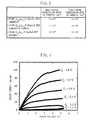
- FIG. 3is a table showing a change in a sheet carrier concentration before and after formation of a SiN gate insulating film in an a-plane AlGaN/GaN HFET as a field effect transistor according to an embodiment of the invention and a c-plane AlGaN/GaN HFET of a comparative example;
- FIG. 4is a graph showing current-voltage characteristics of a field effect transistor according to an embodiment of the invention.
- FIG. 5is a graph showing transfer characteristics of a field effect transistor according to an embodiment of the invention.
- FIG. 6is a graph showing high frequency characteristics of a field effect transistor according to an embodiment of the invention.
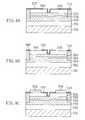
- FIGS. 7A , 7 B, and 7 Care cross-sectional views sequentially illustrating the steps of a method for manufacturing a field effect transistor according to an embodiment of the invention
- FIGS. 8A , 8 B, and 8 Care cross-sectional views sequentially illustrating the steps of a method for manufacturing a field effect transistor according to an embodiment of the invention
- FIG. 9is a cross-sectional view illustrating a step of a method for manufacturing a field effect transistor according to an embodiment of the invention.
- FIGS. 10A , 10 B, and 10 Care cross-sectional views sequentially illustrating the steps of a method for manufacturing a field effect transistor according to a modification of an embodiment of the invention
- FIGS. 11A , 11 B, and 11 Care cross-sectional views sequentially illustrating the steps of a method for manufacturing a field effect transistor according to a modification of an embodiment of the invention
- FIGS. 12A , 12 B, and 12 Care cross-sectional views sequentially illustrating the steps of a method for manufacturing a field effect transistor according to a modification of an embodiment of the invention
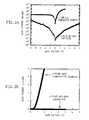
- FIGS. 13A and 13Bare schematic conduction band diagrams illustrating a behavior of a sheet carrier concentration at the AlGaN/GaN interface of a c-plane AlGaN/GaN HFET of a conventional example, where FIG. 13A shows the case in which a gate electrode is provided directly on a c-plane AlGaN/GaN HFET, and FIG. 13B shows the case in which a SiN film is formed between a c-plane AlGaN/GaN HFET and a gate electrode; and
- FIGS. 13C and 13Dare schematic conduction band diagrams illustrating a behavior of a sheet carrier concentration at the AlGaN/GaN interface of an a-plane AlGaN/GaN HFET, where FIG. 13C shows the case in which a gate electrode is provided directly on an a-plane AlGaN/GaN HFET in a comparative example, and FIG. 13D shows the case in which a SiN film is formed between an a-plane AlGaN/GaN HFET and a gate electrode in the invention.
- an a-planeindicates a (11-20) plane
- an r-planeindicates a (1-102) plane
- a c-planeindicates a (0001) plane unless otherwise mentioned.
- a negative sign given to a Miller index of plane orientationindicates inversion of an index following the negative sign.
- FIG. 1shows a cross-sectional structure of an AlGaN/GaN heterojunction field effect transistor having an a-plane as a main surface (hereinafter, simply referred to as an a-plane AlGaN/GaN HFET) according to a first embodiment of the invention.
- the sapphire substrate 101has an r-plane as a main surface, and each of the buffer layer 102 , the undoped GaN layer 103 , the AlN spacer layer 104 , the n-type Al x Ga 1-x N barrier layer 105 , and the n-type GaN cap layer 106 has an a-plane as a main surface.
- the n-type Al x Ga 1-x N barrier layer 105 hereinhas an Al composition of 0.25.
- the spacer layer 104 formed between the GaN layer 103 and the barrier layer 105need not necessarily be provided.
- a part of the cap layer 106is removed by, e.g. a dry etching method to form a recess (opening) exposing the barrier layer 105 from the cap layer 106 .
- a SiN gate insulating film 107 having a thickness of 3 nmis formed so as to cover the side surface and the bottom surface of the recess.
- a high resistance isolation layer 110is formed at both ends of each layer from the cap layer 106 to the upper portion of the GaN layer 103 by implantation of, e.g., boron (B + ) ions.
- the isolation layer 110may be formed by a mesa isolation method or a selective oxidation method.
- a Ti/Al (titanium/aluminum) ohmic electrode (source-drain electrode) 109is formed on both sides of the recess on the cap layer 106 at a distance from the recess.
- a PdSi (palladium silicon) gate electrode 108is formed as a so-called recess gate in the recess in the cap layer 106 with the gate insulating film 107 interposed therebetween.
- the n-type AlGaN barrier layer 105has a thickness of 15 nm.
- a thinner barrier layer 105is formed so that a depletion layer formed under the gate electrode 108 reaches a channel of the GaN layer 103 , the channel can be pinched off without application of a gate voltage.
- a threshold voltage of the normally-off type AlGaN/GaN HFETcan further be increased.
- the thickness of the barrier layer 105is not limited to 15 nm, and the barrier layer 105 may be thinner than 15 nm.
- the MIS gate structureis used in this embodiment.
- a MES (Metal Semiconductor) gate structuremay be used as long as normally-off type characteristics can be obtained.
- an electrode contact resistanceis reduced by forming the n-type GaN cap layer 106 having an a-plane as a main surface by doping n-type impurities at a high concentration, and forming the source/drain electrode 109 on the n-type GaN cap layer 106 .
- a sufficiently low contact resistance of 2.7 ⁇ 10 ⁇ 6 ⁇ cm 2can be obtained between the source/drain electrode 109 and the cap layer 106 . Accordingly, a normally-off type a-plane AlGaN/GaN HFET having a low source-drain series resistance can be obtained.
- the cap layer 106may alternatively be formed by forming n-type doped Al 0.25 Ga 0.75 N/GaN periodically, for example, with seven periods, with a thickness of 50 nm, or may be an In x Al y Ga 1-x-y N (indium aluminum gallium nitride) layer (0 ⁇ x ⁇ 1, 0 ⁇ y ⁇ 1, and 0 ⁇ x+y ⁇ 1).
- a so-called ohmic recess structuremay be formed by forming a recess under the ohmic electrode 109 in the cap layer 106 so that the ohmic electrode 109 contacts the barrier layer 105 .
- Typical dimensions of the field effect transistor of this embodimentare as follows: the gate recess has a width of 0.6 ⁇ m in the gate length direction; the upper portion of the gate electrode 108 has a gate length of 1.0 ⁇ m; and both ends of the upper portion of the gate electrode 108 in the gate length direction overlap the cap layer 106 with a width of 0.2 ⁇ m.
- the field effect transistor of this embodimenthas a narrow recess structure.
- a 2DEG layeris formed near a heterojunction at the interface between the GaN layer 103 and the spacer layer 104 under the gate electrode 108 when a gate bias voltage higher than the threshold voltage is applied.
- electrons serving as carrierstravel through a path formed by the source electrode 109 , the cap layer 106 under the source electrode 109 , the 2DEG layer, the cap layer 106 under the drain electrode 109 , and the drain electrode 109 . Accordingly, in an on state, electrons can travel only in the 2DEG layer as a channel, whereby a low on-state resistance field effect transistor can be implemented. Since the gate electrode 108 and the cap layer 106 contact each other with the SiN gate insulating film 107 interposed therebetween, no significant gate leakage current is generated even when a forward voltage of 5 V or higher is applied.
- a channel resistance and a source resistancecan be reduced by further reducing the width of the gate recess.
- a normally-off type a-plane AlGaN/GaN HFET having a low source-drain series resistancecan thus be produced.
- FIG. 2Bshows gate-drain forward current-voltage characteristics in the a-plane AlGaN/GaN HFET according to this embodiment by a linear scale.
- a forward rising voltageis about 0.5 V in the MES type HFET of the comparative example, while no significant gate leakage current is recognized in the MIS type HFET of the invention even when a forward voltage of 5 V is applied.
- a gate leakage currentcan thus be reduced by using a MIS gate structure.
- the gate insulating film 107is made of SiN in this embodiment.
- the gate insulating filmmay be made of any material such as SiO 2 (silicon dioxide), HfO 2 (hafnium dioxide), Al 2 O 3 (aluminum oxide), or AlN as long as the same effects can be obtained.
- the gate insulating filmmay be a multi-layer film made of a combination of at least two kinds of the above insulating films.
- FIG. 3shows a change in a sheet carrier concentration before and after formation of the SiN gate insulating film 107 in the a-plane AlGaN/GaN HFET of this embodiment and a c-plane AlGaN/GaN HFET of a comparative example.
- An Al compositionis 0.25 and an AlGaN layer has a thickness of 25 nm in the embodiment and the comparative example.
- an Al compositionis 0.4 and an AlGaN layer has a thickness of 6 nm.
- the sheet carrier concentrationhardly changes by formation of SiN.
- the sheet carrier concentrationis approximately doubled by formation of SiN.
- the sheet carrier concentrationis increased to about four times by formation of SiN.
- the sheet carrier concentrationchanges only slightly in the MIS-HFET that includes a nitride semiconductor layer having an a-plane as a main surface as in the invention. Therefore, both a low gate leakage current and a normally-off type operation can be implemented at the same time without taking into consideration a change in a threshold voltage by the MIS structure.
- FIGS. 13A through 13Dare schematic conduction band diagrams illustrating a behavior of a sheet carrier concentration at the AlGaN/GaN interface of an AlGaN/GaN HFET.
- one of the causes that increase a sheet carrier concentration in a c-plane AlGaN/GaN HFET having a SiN film on the surface of an AlGaN layeris as follows: Si becomes donor impurities by Si—N bonding at the SiN/AlGaN interface, whereby positive charges are formed and a surface potential is reduced. As a result, electrons are compensated for at the AlGaN/GaN interface, and the concentration of a 2-dimensional electron gas (2DEG) layer is increased.
- 2DEG2-dimensional electron gas
- FIG. 4shows the relation between a drain current and a drain voltage of the field effect transistor of the embodiment. It can be seen from FIG. 4 that the threshold voltage is +1.3 V and a normally-off type field effect transistor is obtained.
- FIG. 5shows transfer characteristics of the field effect transistor of the embodiment. As shown in FIG. 5 , a maximum drain current I max is 112 mA/mm and a maximum mutual conductance g mmax is 47 mS/mm.
- FIG. 6shows frequency dependencies of a current gain and a maximum stable power gain (MSG) or maximum available power gain (MAG) calculated from a measured S parameter in the field effect transistor of the embodiment. It can be seen that, at a gate voltage V g of 4.5 V and a drain-source voltage V ds of 4.5 V, a current gain cutoff frequency (f T ) and a maximum oscillating frequency (f max ) in the field effect transistor are 2.3 GHz and 4.0 GHz, respectively.
- MSGmaximum stable power gain
- MAGmaximum available power gain
- an a-plane(a (11-20) plane) is used as a main growth surface of each nitride semiconductor layer.
- a (1-100) plane, a (1-101) plane, a (1-102) plane, a (11-22) plane, or a (11-24) plane, or any other orientationsmay be used as long as the same effects can be obtained.
- a sapphire substrate having an r-plane as a main surfaceis used as the substrate 101 .
- the substratemay be made of silicon carbide (SiC), gallium nitride (GaN), silicon (Si), or the like and the substrate may have any orientation as long as the same effects can be obtained.
- FIGS. 7A through 7C , FIGS. 8A through 8C , and FIG. 9show cross-sectional structures sequentially illustrating the steps of a method for manufacturing a field effect transistor according to an embodiment of the invention.
- an AlN buffer layer 702 having a thickness of 500 nm, an undoped GaN layer 703 having a thickness of 3 ⁇ m, an AlN spacer layer 704 having a thickness of 1 nm, an Al 0.25 Ga 0.75 N barrier layer (electron supply layer) 705 having a thickness of 15 nm, and a Si-doped n-type GaN cap layer 706 having a thickness of 50 nmare sequentially epitaxially grown on a main surface of a sapphire substrate 701 by, for example, a MOCVD (Metal Organic Chemical Vapor Deposition) method.
- MOCVDMetal Organic Chemical Vapor Deposition
- the substrate 701has an r-plane as a main surface, and each of the buffer layer 702 , the GaN layer 703 , the spacer layer 704 , the barrier layer 705 , and the cap layer 706 has an a-plane as a main surface (a growth surface).
- a recess(a gate recess) is then formed by selectively etching the cap layer 706 so as to expose the barrier layer 705 by a dry etching method such as an ICP (Inductively Coupled Plasma) method.
- ICPInductively Coupled Plasma
- an isolation layer 710is then formed on both side of the gate recess so that each isolation layer 710 is located at a distance from the gate recess. More specifically, the isolation layer 710 is formed by selectively implanting boron (B + ) ions from the cap layer 706 to the upper portion of the GaN layer 703 so as to selectively increase the resistance of each semiconductor layer.
- the process of increasing the resistanceis not limited to the ion implantation method. For example, a selective thermal oxidation method may alternatively be used.
- a SiN gate insulating film 707 having a thickness of 3 nmis then formed on the whole surface including the wall surface and the bottom surface of the gate recess on the isolation layer 710 and the cap layer 706 by, for example, a plasma CVD (Chemical Vapor Deposition) method.
- the gate insulating film 707may be formed by an MOCVD method instead of the plasma CVD method.
- the cap layer 706is selectively exposed from the gate insulating film 707 by removing the gate insulating film 707 in an ohmic electrode formation region between the gate recess and each isolation layer 710 by a dry etching method. A contact resistance between an ohmic electrode to be formed and the cap layer 706 is thus reduced.
- a Ti/Al ohmic electrode (source/drain electrode) 709is formed on the exposed cap layer 706 by, for example, a sputtering method and a lift-off method. A sintering process is then conducted.
- a PdSi gate electrode 708is formed in the gate recess in the cap layer 706 and on the periphery of the gate recess with the gate insulating film 707 interposed therebetween by, for example, a sputtering method and a lift-off method.
- the substrate 701 for epitaxial growthis a sapphire substrate having an r-plane as a main surface.
- the inventionis not limited to sapphire having an r-plane as a main surface.
- the substrate 701may be made of SiC, GaN, Si, or the like and any orientation may be used as a main surface of the substrate 701 as long as the same effects as those obtained by sapphire having an r-plane as a main surface can be obtained.
- FIGS. 10A through 10C , FIGS. 11A through 11C , and FIGS. 12A through 12Cshow cross-sectional structures sequentially illustrating the steps of the method for manufacturing a field effect transistor according to the modification of the embodiment.
- an AlN buffer layer 802 having a thickness of 500 nm, an undoped GaN layer 803 having a thickness of 3 ⁇ m, an AlN spacer layer 804 having a thickness of 1 nm, and an Al 0.25 Ga 0.75 N barrier layer (electron supply layer) 805 having a thickness of 15 nmare sequentially epitaxially grown on a main surface of a sapphire substrate 801 by, for example, a MOCVD method.
- the substrate 801has an r-plane as a main surface
- each of the buffer layer 802 , the GaN layer 803 , the spacer layer 804 , and the barrier layer 805has an a-plane as a main surface (a growth surface).
- a SiO 2 mask film 811 having a thickness of 100 nmis then selectively formed in a gate recess formation region on the barrier layer 805 .
- a Si-doped n-type GaN cap layer 806 having an a-plane as a main surfaceis then formed with a thickness of 50 nm on the barrier layer 805 having the mask film 811 formed thereon by a MOCVD method.
- the cap layer 806is grown on the barrier layer 805 except on the mask film 811 .
- a recess (a gate recess) exposing the barrier layer 805is then formed in the cap layer 806 by removing the mask film 811 with hydrofluoric acid (HF) or the like.
- HFhydrofluoric acid
- the exposed surface of the barrier layer 805 from the cap layer 806is not subjected to damage from plasma processing that is conducted in a dry etching method.
- an isolation layer 810is then formed on both side of the gate recess so that each isolation layer 810 is located at a distance from the gate recess. More specifically, the isolation layer 810 is formed by selectively implanting boron (B + ) ions from the cap layer 806 to the upper portion of the GaN layer 803 so as to selectively increase the resistance of each semiconductor layer.
- the process of increasing the resistanceis not limited to the ion implantation method. For example, a selective thermal oxidation method may alternatively be used.
- a Ti/Al ohmic electrode (source/drain electrode) 809is selectively formed in a region between the gate recess and each isolation layer 810 on the cap layer 806 by, for example, a sputtering method and a lift-off method. A sintering process is then conducted.
- a SiN gate insulating film 807 having a thickness of 3 nmis then formed on the whole surface including the wall surface and the bottom surface of the gate recess on the isolation layer 810 , the cap layer 806 , and the ohmic electrode 809 by, for example, a plasma CVD method.
- the gate insulating film 807may be formed by an MOCVD method instead of the plasma CVD method.
- a PdSi gate electrode 808is then formed in the gate recess in the cap layer 806 and on the periphery of the gate recess with the gate insulating film 807 interposed therebetween by, for example, a sputtering method and a lift-off method.
- a contact hole exposing the top surface of each ohmic electrode 809is then selectively formed by removing the gate insulating film 807 on each ohmic electrode 809 by a dry etching method.
- the barrier layer 805is not subjected to damage from plasma processing when the gate recess exposing the barrier layer 805 is formed in the cap layer 806 . Therefore, a low gate leakage current normally-off type field effect transistor can be obtained.
- the substrate 801 for epitaxial growthis a sapphire substrate having an r-plane as a main surface.
- the inventionis not limited to sapphire having an r-plane as a main surface.
- the substrate 801may be made of SiC, GaN, Si, or the like and any orientation may be used as a main surface of the substrate 801 as long as the same effects as those obtained by sapphire having an r-plane as a main surface can be obtained.
- a low gate leakage current normally-off type nitride semiconductor field effect transistorthat is applicable to, for example, a high power transistor can be implemented by the invention.
Landscapes
- Junction Field-Effect Transistors (AREA)
Abstract
Description
Claims (8)
Applications Claiming Priority (2)
| Application Number | Priority Date | Filing Date | Title |
|---|---|---|---|
| JP2007-111451 | 2007-04-20 | ||
| JP2007111451AJP2008270521A (en) | 2007-04-20 | 2007-04-20 | Field effect transistor |
Publications (2)
| Publication Number | Publication Date |
|---|---|
| US20080258243A1 US20080258243A1 (en) | 2008-10-23 |
| US7956383B2true US7956383B2 (en) | 2011-06-07 |
Family
ID=39871354
Family Applications (1)
| Application Number | Title | Priority Date | Filing Date |
|---|---|---|---|
| US12/060,505Active2029-04-29US7956383B2 (en) | 2007-04-20 | 2008-04-01 | Field effect transistor |
Country Status (2)
| Country | Link |
|---|---|
| US (1) | US7956383B2 (en) |
| JP (1) | JP2008270521A (en) |
Cited By (18)
| Publication number | Priority date | Publication date | Assignee | Title |
|---|---|---|---|---|
| US20100127275A1 (en)* | 2008-11-26 | 2010-05-27 | Furukawa Electric Co., Ltd. | Gan-based field effect transistor and method of manufacturing the same |
| US20100244045A1 (en)* | 2005-03-02 | 2010-09-30 | Panasonic Corporation | Semiconductor device and method for manufacturing the same |
| US20100252816A1 (en)* | 2009-04-01 | 2010-10-07 | Taiwan Semiconductor Manufacturing Company, Ltd. | High-Mobility Multiple-Gate Transistor with Improved On-to-Off Current Ratio |
| US20100252862A1 (en)* | 2009-04-01 | 2010-10-07 | Chih-Hsin Ko | Source/Drain Engineering of Devices with High-Mobility Channels |
| US20100276668A1 (en)* | 2009-04-30 | 2010-11-04 | Chih-Hsin Ko | Reducing Source/Drain Resistance of III-V Based Transistors |
| US20100301392A1 (en)* | 2009-06-01 | 2010-12-02 | Chih-Hsin Ko | Source/Drain Re-Growth for Manufacturing III-V Based Transistors |
| US20100301390A1 (en)* | 2009-05-29 | 2010-12-02 | Chih-Hsin Ko | Gradient Ternary or Quaternary Multiple-Gate Transistor |
| US20110133205A1 (en)* | 2009-12-08 | 2011-06-09 | Sharp Kabushiki Kaisha | Field-effect transistor |
| US20110156050A1 (en)* | 2009-12-28 | 2011-06-30 | Sumitomo Electric Industries, Ltd. | Semiconductor device and method for producing the same |
| US20140361309A1 (en)* | 2008-04-23 | 2014-12-11 | Transphorm Inc. | Enhancement Mode III-N HEMTs |
| US9318593B2 (en) | 2014-07-21 | 2016-04-19 | Transphorm Inc. | Forming enhancement mode III-nitride devices |
| US9536966B2 (en) | 2014-12-16 | 2017-01-03 | Transphorm Inc. | Gate structures for III-N devices |
| US9536967B2 (en) | 2014-12-16 | 2017-01-03 | Transphorm Inc. | Recessed ohmic contacts in a III-N device |
| US9590060B2 (en) | 2013-03-13 | 2017-03-07 | Transphorm Inc. | Enhancement-mode III-nitride devices |
| US9704968B2 (en) | 2011-12-28 | 2017-07-11 | Taiwan Semiconductor Manufacturing Company, Ltd. | Method of forming a high electron mobility transistor |
| US10224401B2 (en) | 2016-05-31 | 2019-03-05 | Transphorm Inc. | III-nitride devices including a graded depleting layer |
| US20200052074A1 (en)* | 2015-11-24 | 2020-02-13 | Sumitomo Electric Industries, Ltd. | Silicon carbide epitaxial substrate and method of manufacturing silicon carbide semiconductor device |
| US11322599B2 (en) | 2016-01-15 | 2022-05-03 | Transphorm Technology, Inc. | Enhancement mode III-nitride devices having an Al1-xSixO gate insulator |
Families Citing this family (36)
| Publication number | Priority date | Publication date | Assignee | Title |
|---|---|---|---|---|
| US7800116B2 (en)* | 2007-03-29 | 2010-09-21 | Panasonic Corporation | Group III-nitride semiconductor device with a cap layer |
| JP5032965B2 (en)* | 2007-12-10 | 2012-09-26 | パナソニック株式会社 | Nitride semiconductor transistor and manufacturing method thereof |
| EP2161754A3 (en)* | 2008-09-03 | 2010-06-16 | Kabushiki Kaisha Toshiba | A semiconductor device and fabrication method for the same |
| JP5549081B2 (en)* | 2009-01-16 | 2014-07-16 | 日本電気株式会社 | Semiconductor device and manufacturing method thereof |
| JP5195532B2 (en)* | 2009-03-04 | 2013-05-08 | 住友電気工業株式会社 | Compound semiconductor electronic device and compound semiconductor integrated electronic device |
| JP2010212596A (en)* | 2009-03-12 | 2010-09-24 | Sharp Corp | Field effect transistor |
| JP5537555B2 (en) | 2009-09-29 | 2014-07-02 | 株式会社東芝 | Semiconductor device |
| JP2011077386A (en)* | 2009-09-30 | 2011-04-14 | Sumitomo Electric Ind Ltd | High electron mobility transistor, epitaxial substrate, and method of manufacturing high electron mobility transistor |
| JP2011082216A (en) | 2009-10-02 | 2011-04-21 | Fujitsu Ltd | Compound semiconductor device and method for manufacturing the same |
| TWI420578B (en)* | 2010-01-14 | 2013-12-21 | Great Power Semiconductor Corp | Trenched power semiconductor structure with reduced gate impedance and fabrication method thereof |
| JP5635803B2 (en) | 2010-05-07 | 2014-12-03 | トランスフォーム・ジャパン株式会社 | Compound semiconductor device manufacturing method and compound semiconductor device |
| US8344421B2 (en) | 2010-05-11 | 2013-01-01 | Iqe Rf, Llc | Group III-nitride enhancement mode field effect devices and fabrication methods |
| JP5672868B2 (en)* | 2010-08-31 | 2015-02-18 | 富士通株式会社 | Compound semiconductor device and manufacturing method thereof |
| JP2012114242A (en)* | 2010-11-25 | 2012-06-14 | Mitsubishi Electric Corp | Heterojunction field effect transistor and method of manufacturing the same |
| JP5654884B2 (en)* | 2011-01-26 | 2015-01-14 | 株式会社東芝 | Manufacturing method of nitride semiconductor device |
| JP2012169470A (en)* | 2011-02-15 | 2012-09-06 | Nippon Telegr & Teleph Corp <Ntt> | Semiconductor device and manufacturing method of the same |
| US8653559B2 (en) | 2011-06-29 | 2014-02-18 | Hrl Laboratories, Llc | AlGaN/GaN hybrid MOS-HFET |
| KR20130004760A (en) | 2011-07-04 | 2013-01-14 | 삼성전자주식회사 | Power devices and methods for manufacturing the same |
| JP6017125B2 (en)* | 2011-09-16 | 2016-10-26 | ルネサスエレクトロニクス株式会社 | Semiconductor device and manufacturing method of semiconductor device |
| US9018677B2 (en)* | 2011-10-11 | 2015-04-28 | Taiwan Semiconductor Manufacturing Company, Ltd. | Semiconductor structure and method of forming the same |
| US9601638B2 (en)* | 2011-10-19 | 2017-03-21 | Nxp Usa, Inc. | GaN-on-Si switch devices |
| US8963162B2 (en)* | 2011-12-28 | 2015-02-24 | Taiwan Semiconductor Manufacturing Company, Ltd. | High electron mobility transistor |
| US9076850B2 (en) | 2012-07-30 | 2015-07-07 | Samsung Electronics Co., Ltd. | High electron mobility transistor |
| KR20140066015A (en)* | 2012-11-22 | 2014-05-30 | 삼성전자주식회사 | Hetero junction field effect transistor and method for manufacturing the same |
| JP5716765B2 (en)* | 2013-02-07 | 2015-05-13 | 住友電気工業株式会社 | Epitaxial substrate |
| US8916427B2 (en)* | 2013-05-03 | 2014-12-23 | Texas Instruments Incorporated | FET dielectric reliability enhancement |
| JP6548065B2 (en)* | 2014-01-24 | 2019-07-24 | 国立大学法人 名古屋工業大学 | Normally-off type nitride semiconductor field effect transistor with improved ohmic characteristics |
| TWI556321B (en)* | 2014-04-23 | 2016-11-01 | 穩懋半導體股份有限公司 | Process for implanting boron isolation structure with high electron mobility transistor |
| US10276712B2 (en) | 2014-05-29 | 2019-04-30 | Hrl Laboratories, Llc | III-nitride field-effect transistor with dual gates |
| TWI577046B (en)* | 2014-12-23 | 2017-04-01 | 錼創科技股份有限公司 | Semiconductor light emitting element and manufacturing method thereof |
| US9812532B1 (en)* | 2015-08-28 | 2017-11-07 | Hrl Laboratories, Llc | III-nitride P-channel transistor |
| JP6641876B2 (en)* | 2015-10-21 | 2020-02-05 | 住友電気工業株式会社 | Method for manufacturing semiconductor device |
| CN108292678B (en) | 2015-11-19 | 2021-07-06 | Hrl实验室有限责任公司 | Ill-nitride field effect transistor with double gate |
| CN107230720A (en)* | 2016-03-25 | 2017-10-03 | 北京大学 | The preparation method of gallium nitride heterojunction field-effect transistor |
| JP6658253B2 (en)* | 2016-04-21 | 2020-03-04 | 富士通株式会社 | Semiconductor device and method of manufacturing semiconductor device |
| US11569182B2 (en)* | 2019-10-22 | 2023-01-31 | Analog Devices, Inc. | Aluminum-based gallium nitride integrated circuits |
Citations (3)
| Publication number | Priority date | Publication date | Assignee | Title |
|---|---|---|---|---|
| US20060124962A1 (en)* | 2004-12-09 | 2006-06-15 | Matsushita Electric Industrial Co., Ltd. | Field effect transistor and method for fabricating the same |
| JP2006173294A (en) | 2004-12-15 | 2006-06-29 | Nippon Telegr & Teleph Corp <Ntt> | Semiconductor device |
| US20060157729A1 (en)* | 2005-01-14 | 2006-07-20 | Matsushita Electric Industrial Co., Ltd. | Semiconductor device |
Family Cites Families (9)
| Publication number | Priority date | Publication date | Assignee | Title |
|---|---|---|---|---|
| JP2003347315A (en)* | 2002-05-23 | 2003-12-05 | Sharp Corp | Semiconductor device, manufacturing method thereof, power amplifier, and radio communication system |
| JP2006013277A (en)* | 2004-06-29 | 2006-01-12 | Hitachi Cable Ltd | Nitride-based compound semiconductor crystal, manufacturing method thereof, and semiconductor device |
| EP1801865A4 (en)* | 2004-08-27 | 2009-11-04 | Nat Inst Inf & Comm Tech | GALLIUM-NITRIDE FIELD EFFECT TRANSISTOR AND METHOD FOR PRODUCING THE SAME |
| JP4883931B2 (en)* | 2005-04-26 | 2012-02-22 | 京セラ株式会社 | Manufacturing method of semiconductor laminated substrate |
| JP4869576B2 (en)* | 2004-09-29 | 2012-02-08 | 新日本無線株式会社 | Nitride semiconductor device and manufacturing method thereof |
| JP2006222414A (en)* | 2005-01-14 | 2006-08-24 | Matsushita Electric Ind Co Ltd | Semiconductor device |
| JP2007042779A (en)* | 2005-08-02 | 2007-02-15 | Nippon Telegr & Teleph Corp <Ntt> | T-shaped gate structure nitride field effect transistor and method of manufacturing the same |
| JP2007081096A (en)* | 2005-09-14 | 2007-03-29 | Nec Corp | Semiconductor device |
| JP2007088185A (en)* | 2005-09-21 | 2007-04-05 | Toshiba Corp | Semiconductor device and manufacturing method thereof |
- 2007
- 2007-04-20JPJP2007111451Apatent/JP2008270521A/enactivePending
- 2008
- 2008-04-01USUS12/060,505patent/US7956383B2/enactiveActive
Patent Citations (3)
| Publication number | Priority date | Publication date | Assignee | Title |
|---|---|---|---|---|
| US20060124962A1 (en)* | 2004-12-09 | 2006-06-15 | Matsushita Electric Industrial Co., Ltd. | Field effect transistor and method for fabricating the same |
| JP2006173294A (en) | 2004-12-15 | 2006-06-29 | Nippon Telegr & Teleph Corp <Ntt> | Semiconductor device |
| US20060157729A1 (en)* | 2005-01-14 | 2006-07-20 | Matsushita Electric Industrial Co., Ltd. | Semiconductor device |
Non-Patent Citations (2)
| Title |
|---|
| Higashiwaki, M. et al., "AlGaN/GaN Heterostructure Field-Effect Transistors with Current Gain Cut-off Frequency of 152 GHz on Sapphire Substrates," J.J. Appl. Phys. vol. 44, pp. L475-L478, 2005. |
| Wang, R. et al., "Enhancement-Mode Si3N4/AlGaN/GaN MISHFETs," IEEE Electron Device Lett., vol. 27, No. 10, pp. 793-795, Oct. 2006. |
Cited By (47)
| Publication number | Priority date | Publication date | Assignee | Title |
|---|---|---|---|---|
| US20100244045A1 (en)* | 2005-03-02 | 2010-09-30 | Panasonic Corporation | Semiconductor device and method for manufacturing the same |
| US8710548B2 (en)* | 2005-03-02 | 2014-04-29 | Panasonic Corporation | Semiconductor device and method for manufacturing the same |
| US9941399B2 (en) | 2008-04-23 | 2018-04-10 | Transphorm Inc. | Enhancement mode III-N HEMTs |
| US9437708B2 (en) | 2008-04-23 | 2016-09-06 | Transphorm Inc. | Enhancement mode III-N HEMTs |
| US9196716B2 (en)* | 2008-04-23 | 2015-11-24 | Transphorm Inc. | Enhancement mode III-N HEMTs |
| US20140361309A1 (en)* | 2008-04-23 | 2014-12-11 | Transphorm Inc. | Enhancement Mode III-N HEMTs |
| US8330167B2 (en)* | 2008-11-26 | 2012-12-11 | Furukawa Electric Co., Ltd | GaN-based field effect transistor and method of manufacturing the same |
| US20100127275A1 (en)* | 2008-11-26 | 2010-05-27 | Furukawa Electric Co., Ltd. | Gan-based field effect transistor and method of manufacturing the same |
| US10109748B2 (en) | 2009-04-01 | 2018-10-23 | Taiwan Semiconductor Manufacturing Company, Ltd. | High-mobility multiple-gate transistor with improved on-to-off current ratio |
| US8927371B2 (en) | 2009-04-01 | 2015-01-06 | Taiwan Semiconductor Manufacturing Company, Ltd. | High-mobility multiple-gate transistor with improved on-to-off current ratio |
| US9590068B2 (en) | 2009-04-01 | 2017-03-07 | Taiwan Semiconductor Manufacturing Company, Ltd. | High-mobility multiple-gate transistor with improved on-to-off current ratio |
| US20100252862A1 (en)* | 2009-04-01 | 2010-10-07 | Chih-Hsin Ko | Source/Drain Engineering of Devices with High-Mobility Channels |
| US8674341B2 (en) | 2009-04-01 | 2014-03-18 | Taiwan Semiconductor Manufacturing Company, Ltd. | High-mobility multiple-gate transistor with improved on-to-off current ratio |
| US20100252816A1 (en)* | 2009-04-01 | 2010-10-07 | Taiwan Semiconductor Manufacturing Company, Ltd. | High-Mobility Multiple-Gate Transistor with Improved On-to-Off Current Ratio |
| US8816391B2 (en) | 2009-04-01 | 2014-08-26 | Taiwan Semiconductor Manufacturing Company, Ltd. | Source/drain engineering of devices with high-mobility channels |
| US8455860B2 (en) | 2009-04-30 | 2013-06-04 | Taiwan Semiconductor Manufacturing Company, Ltd. | Reducing source/drain resistance of III-V based transistors |
| US8674408B2 (en) | 2009-04-30 | 2014-03-18 | Taiwan Semiconductor Manufacturing Company, Ltd. | Reducing source/drain resistance of III-V based transistors |
| US20100276668A1 (en)* | 2009-04-30 | 2010-11-04 | Chih-Hsin Ko | Reducing Source/Drain Resistance of III-V Based Transistors |
| US20100301390A1 (en)* | 2009-05-29 | 2010-12-02 | Chih-Hsin Ko | Gradient Ternary or Quaternary Multiple-Gate Transistor |
| US10269970B2 (en) | 2009-05-29 | 2019-04-23 | Taiwan Semiconductor Manufacturing Company, Ltd. | Gradient ternary or quaternary multiple-gate transistor |
| US9768305B2 (en) | 2009-05-29 | 2017-09-19 | Taiwan Semiconductor Manufacturing Company, Ltd. | Gradient ternary or quaternary multiple-gate transistor |
| US9006788B2 (en) | 2009-06-01 | 2015-04-14 | Taiwan Semiconductor Manufacturing Company, Ltd. | Source/drain re-growth for manufacturing III-V based transistors |
| US20100301392A1 (en)* | 2009-06-01 | 2010-12-02 | Chih-Hsin Ko | Source/Drain Re-Growth for Manufacturing III-V Based Transistors |
| US8617976B2 (en) | 2009-06-01 | 2013-12-31 | Taiwan Semiconductor Manufacturing Company, Ltd. | Source/drain re-growth for manufacturing III-V based transistors |
| US20110133205A1 (en)* | 2009-12-08 | 2011-06-09 | Sharp Kabushiki Kaisha | Field-effect transistor |
| US20110156050A1 (en)* | 2009-12-28 | 2011-06-30 | Sumitomo Electric Industries, Ltd. | Semiconductor device and method for producing the same |
| US8405125B2 (en)* | 2009-12-28 | 2013-03-26 | Sumitomo Electric Industries, Ltd. | Semiconductor device and method for producing the same |
| US9704968B2 (en) | 2011-12-28 | 2017-07-11 | Taiwan Semiconductor Manufacturing Company, Ltd. | Method of forming a high electron mobility transistor |
| US10741665B2 (en) | 2011-12-28 | 2020-08-11 | Taiwan Semiconductor Manufacturing Company, Ltd. | Method of forming a high electron mobility transistor |
| US12230690B2 (en) | 2011-12-28 | 2025-02-18 | Taiwan Semiconductor Manufacturing Company, Ltd. | Method of forming a high electron mobility transistor |
| US11804538B2 (en) | 2011-12-28 | 2023-10-31 | Taiwan Semiconductor Manufacturing Company, Ltd. | Method of forming a high electron mobility transistor |
| US11404557B2 (en) | 2011-12-28 | 2022-08-02 | Taiwan Semiconductor Manufacturing Company, Ltd. | Method of forming a high electron mobility transistor |
| US10050117B2 (en) | 2011-12-28 | 2018-08-14 | Taiwan Semiconductor Manufacturing Company, Ltd. | Method of forming a high electron mobility transistor |
| US10535763B2 (en) | 2013-03-13 | 2020-01-14 | Transphorm Inc. | Enhancement-mode III-nitride devices |
| US10043898B2 (en) | 2013-03-13 | 2018-08-07 | Transphorm Inc. | Enhancement-mode III-nitride devices |
| US9590060B2 (en) | 2013-03-13 | 2017-03-07 | Transphorm Inc. | Enhancement-mode III-nitride devices |
| US9318593B2 (en) | 2014-07-21 | 2016-04-19 | Transphorm Inc. | Forming enhancement mode III-nitride devices |
| US9935190B2 (en) | 2014-07-21 | 2018-04-03 | Transphorm Inc. | Forming enhancement mode III-nitride devices |
| US9536967B2 (en) | 2014-12-16 | 2017-01-03 | Transphorm Inc. | Recessed ohmic contacts in a III-N device |
| US9536966B2 (en) | 2014-12-16 | 2017-01-03 | Transphorm Inc. | Gate structures for III-N devices |
| US10770550B2 (en)* | 2015-11-24 | 2020-09-08 | Sumitomo Electric Industries, Ltd. | Silicon carbide epitaxial substrate having grooves extending along main surface and method of manufacturing silicon carbide semiconductor device |
| US11004941B2 (en) | 2015-11-24 | 2021-05-11 | Sumitomo Electric Industries, Ltd. | Silicon carbide epitaxial substrate having grooves extending along main surface and method of manufacturing silicon carbide semiconductor device |
| US20200052074A1 (en)* | 2015-11-24 | 2020-02-13 | Sumitomo Electric Industries, Ltd. | Silicon carbide epitaxial substrate and method of manufacturing silicon carbide semiconductor device |
| US11322599B2 (en) | 2016-01-15 | 2022-05-03 | Transphorm Technology, Inc. | Enhancement mode III-nitride devices having an Al1-xSixO gate insulator |
| US11121216B2 (en) | 2016-05-31 | 2021-09-14 | Transphorm Technology, Inc. | III-nitride devices including a graded depleting layer |
| US10224401B2 (en) | 2016-05-31 | 2019-03-05 | Transphorm Inc. | III-nitride devices including a graded depleting layer |
| US10629681B2 (en) | 2016-05-31 | 2020-04-21 | Transphorm Technology, Inc. | III-nitride devices including a graded depleting layer |
Also Published As
| Publication number | Publication date |
|---|---|
| JP2008270521A (en) | 2008-11-06 |
| US20080258243A1 (en) | 2008-10-23 |
Similar Documents
| Publication | Publication Date | Title |
|---|---|---|
| US7956383B2 (en) | Field effect transistor | |
| US20220416072A1 (en) | Nitride semiconductor device and method of manufacturing the same | |
| US8101972B2 (en) | Nitride semiconductor device and method for fabricating the same | |
| JP5114947B2 (en) | Nitride semiconductor device and manufacturing method thereof | |
| JP5653607B2 (en) | GaN-based field effect transistor and manufacturing method thereof | |
| US8390029B2 (en) | Semiconductor device for reducing and/or preventing current collapse | |
| JP5810293B2 (en) | Nitride semiconductor device | |
| US8716756B2 (en) | Semiconductor device | |
| KR101365302B1 (en) | Compound semiconductor device and method for fabricating the same | |
| JP5495257B2 (en) | Group III nitride field effect transistor and method of manufacturing the same | |
| JP5566670B2 (en) | GaN-based field effect transistor | |
| JP5126733B2 (en) | Field effect transistor and manufacturing method thereof | |
| JPH10223901A (en) | Field effect transistor and method of manufacturing the same | |
| US10727328B2 (en) | Semiconductor device and manufacturing method thereof | |
| WO2009110254A1 (en) | Field effect transistor and method for manufacturing the same | |
| JP5546104B2 (en) | GaN-based field effect transistor | |
| US8283700B2 (en) | Field effect transistor and manufacturing method thereof | |
| JP2010153748A (en) | Method of manufacturing field effect semiconductor device | |
| KR101935928B1 (en) | High Electron Mobility Transistor having Reduced Gate Leakage Current | |
| JP2006286698A (en) | Electronic device and power converter | |
| JP2010267881A (en) | Field effect transistor and manufacturing method thereof | |
| JP2015204425A (en) | Field effect transistor and manufacturing method thereof |
Legal Events
| Date | Code | Title | Description |
|---|---|---|---|
| AS | Assignment | Owner name:MATSUSHITA ELECTRIC INDUSTRIAL CO., LTD., JAPAN Free format text:ASSIGNMENT OF ASSIGNORS INTEREST;ASSIGNORS:KURODA, MASAYUKI;UEDA, TETSUZO;REEL/FRAME:021260/0227 Effective date:20080311 | |
| AS | Assignment | Owner name:PANASONIC CORPORATION, JAPAN Free format text:CHANGE OF NAME;ASSIGNOR:MATSUSHITA ELECTRIC INDUSTRIAL CO., LTD.;REEL/FRAME:021897/0606 Effective date:20081001 Owner name:PANASONIC CORPORATION,JAPAN Free format text:CHANGE OF NAME;ASSIGNOR:MATSUSHITA ELECTRIC INDUSTRIAL CO., LTD.;REEL/FRAME:021897/0606 Effective date:20081001 | |
| STCF | Information on status: patent grant | Free format text:PATENTED CASE | |
| FEPP | Fee payment procedure | Free format text:PAYOR NUMBER ASSIGNED (ORIGINAL EVENT CODE: ASPN); ENTITY STATUS OF PATENT OWNER: LARGE ENTITY | |
| FPAY | Fee payment | Year of fee payment:4 | |
| MAFP | Maintenance fee payment | Free format text:PAYMENT OF MAINTENANCE FEE, 8TH YEAR, LARGE ENTITY (ORIGINAL EVENT CODE: M1552); ENTITY STATUS OF PATENT OWNER: LARGE ENTITY Year of fee payment:8 | |
| REFU | Refund | Free format text:REFUND - PAYMENT OF MAINTENANCE FEEM 8TH YEAR, MICRO ENTITY (ORIGINAL EVENT CODE: R3552); ENTITY STATUS OF PATENT OWNER: LARGE ENTITY Free format text:REFUND - SURCHARGE FOR LATE PAYMENT, MICRO ENTITY (ORIGINAL EVENT CODE: R3555); ENTITY STATUS OF PATENT OWNER: LARGE ENTITY | |
| FEPP | Fee payment procedure | Free format text:SURCHARGE FOR LATE PAYMENT, MICRO ENTITY (ORIGINAL EVENT CODE: M3555); ENTITY STATUS OF PATENT OWNER: LARGE ENTITY | |
| MAFP | Maintenance fee payment | Free format text:PAYMENT OF MAINTENANCE FEE, 8TH YEAR, MICRO ENTITY (ORIGINAL EVENT CODE: M3552); ENTITY STATUS OF PATENT OWNER: LARGE ENTITY Year of fee payment:8 | |
| MAFP | Maintenance fee payment | Free format text:PAYMENT OF MAINTENANCE FEE, 12TH YEAR, LARGE ENTITY (ORIGINAL EVENT CODE: M1553); ENTITY STATUS OF PATENT OWNER: LARGE ENTITY Year of fee payment:12 |