US7955972B2 - Methods for growing low-resistivity tungsten for high aspect ratio and small features - Google Patents
Methods for growing low-resistivity tungsten for high aspect ratio and small featuresDownload PDFInfo
- Publication number
- US7955972B2 US7955972B2US12/030,645US3064508AUS7955972B2US 7955972 B2US7955972 B2US 7955972B2US 3064508 AUS3064508 AUS 3064508AUS 7955972 B2US7955972 B2US 7955972B2
- Authority
- US
- United States
- Prior art keywords
- tungsten
- feature
- nucleation layer
- layer
- substrate
- Prior art date
- Legal status (The legal status is an assumption and is not a legal conclusion. Google has not performed a legal analysis and makes no representation as to the accuracy of the status listed.)
- Expired - Fee Related
Links
- WFKWXMTUELFFGS-UHFFFAOYSA-NtungstenChemical compound[W]WFKWXMTUELFFGS-UHFFFAOYSA-N0.000titleclaimsabstractdescription166
- 239000010937tungstenSubstances0.000titleclaimsabstractdescription166
- 229910052721tungstenInorganic materials0.000titleclaimsabstractdescription166
- 238000000034methodMethods0.000titleclaimsabstractdescription113
- 238000010899nucleationMethods0.000claimsabstractdescription120
- 230000006911nucleationEffects0.000claimsabstractdescription118
- 230000008569processEffects0.000claimsabstractdescription63
- 238000000151depositionMethods0.000claimsabstractdescription48
- 239000000758substrateSubstances0.000claimsabstractdescription48
- 238000005229chemical vapour depositionMethods0.000claimsabstractdescription32
- 239000002243precursorSubstances0.000claimsabstractdescription26
- 229910052796boronInorganic materials0.000claimsabstractdescription22
- ZOXJGFHDIHLPTG-UHFFFAOYSA-NBoronChemical compound[B]ZOXJGFHDIHLPTG-UHFFFAOYSA-N0.000claimsabstractdescription21
- UFHFLCQGNIYNRP-UHFFFAOYSA-NHydrogenChemical compound[H][H]UFHFLCQGNIYNRP-UHFFFAOYSA-N0.000claimsabstractdescription19
- 239000001257hydrogenSubstances0.000claimsabstractdescription17
- 229910052739hydrogenInorganic materials0.000claimsabstractdescription17
- 239000003638chemical reducing agentSubstances0.000claimsabstractdescription14
- 230000008021depositionEffects0.000claimsdescription35
- 239000000376reactantSubstances0.000claimsdescription6
- 230000015572biosynthetic processEffects0.000claimsdescription5
- 238000010438heat treatmentMethods0.000claims2
- 229920006395saturated elastomerPolymers0.000claims1
- 239000007789gasSubstances0.000abstractdescription22
- 230000009467reductionEffects0.000abstractdescription3
- 239000010410layerSubstances0.000description130
- 238000006243chemical reactionMethods0.000description16
- XKRFYHLGVUSROY-UHFFFAOYSA-NArgonChemical compound[Ar]XKRFYHLGVUSROY-UHFFFAOYSA-N0.000description10
- 229910009035WF6Inorganic materials0.000description10
- NXHILIPIEUBEPD-UHFFFAOYSA-Htungsten hexafluorideChemical compoundF[W](F)(F)(F)(F)FNXHILIPIEUBEPD-UHFFFAOYSA-H0.000description10
- 235000012431wafersNutrition0.000description9
- IJGRMHOSHXDMSA-UHFFFAOYSA-NAtomic nitrogenChemical compoundN#NIJGRMHOSHXDMSA-UHFFFAOYSA-N0.000description8
- 238000005137deposition processMethods0.000description8
- 238000000231atomic layer depositionMethods0.000description7
- 239000012159carrier gasSubstances0.000description7
- 239000010936titaniumSubstances0.000description6
- RTAQQCXQSZGOHL-UHFFFAOYSA-NTitaniumChemical compound[Ti]RTAQQCXQSZGOHL-UHFFFAOYSA-N0.000description5
- 229910052786argonInorganic materials0.000description5
- UORVGPXVDQYIDP-UHFFFAOYSA-NboraneChemical compoundBUORVGPXVDQYIDP-UHFFFAOYSA-N0.000description5
- 238000010926purgeMethods0.000description5
- 229910052719titaniumInorganic materials0.000description5
- BLRPTPMANUNPDV-UHFFFAOYSA-NSilaneChemical compound[SiH4]BLRPTPMANUNPDV-UHFFFAOYSA-N0.000description4
- 239000000463materialSubstances0.000description4
- 239000000203mixtureSubstances0.000description4
- 229910052757nitrogenInorganic materials0.000description4
- 239000004065semiconductorSubstances0.000description4
- 229910000077silaneInorganic materials0.000description4
- XUIMIQQOPSSXEZ-UHFFFAOYSA-NSiliconChemical compound[Si]XUIMIQQOPSSXEZ-UHFFFAOYSA-N0.000description3
- 230000008901benefitEffects0.000description3
- 229910000085boraneInorganic materials0.000description3
- 238000010586diagramMethods0.000description3
- 230000004048modificationEffects0.000description3
- 238000012986modificationMethods0.000description3
- 238000005240physical vapour depositionMethods0.000description3
- 229910052710siliconInorganic materials0.000description3
- 239000010703siliconSubstances0.000description3
- VYPSYNLAJGMNEJ-UHFFFAOYSA-NSilicium dioxideChemical compoundO=[Si]=OVYPSYNLAJGMNEJ-UHFFFAOYSA-N0.000description2
- NRTOMJZYCJJWKI-UHFFFAOYSA-NTitanium nitrideChemical compound[Ti]#NNRTOMJZYCJJWKI-UHFFFAOYSA-N0.000description2
- 229910008940W(CO)6Inorganic materials0.000description2
- 229910003091WCl6Inorganic materials0.000description2
- 230000004075alterationEffects0.000description2
- -1boron halidesChemical class0.000description2
- 229910052751metalInorganic materials0.000description2
- 239000002184metalSubstances0.000description2
- KPGXUAIFQMJJFB-UHFFFAOYSA-Htungsten hexachlorideChemical compoundCl[W](Cl)(Cl)(Cl)(Cl)ClKPGXUAIFQMJJFB-UHFFFAOYSA-H0.000description2
- 239000011800void materialSubstances0.000description2
- 229910015844BCl3Inorganic materials0.000description1
- 230000004913activationEffects0.000description1
- 230000006978adaptationEffects0.000description1
- 238000004630atomic force microscopyMethods0.000description1
- 239000013590bulk materialSubstances0.000description1
- 230000015556catabolic processEffects0.000description1
- 239000013626chemical specieSubstances0.000description1
- 230000003247decreasing effectEffects0.000description1
- 238000006731degradation reactionMethods0.000description1
- ZOCHARZZJNPSEU-UHFFFAOYSA-NdiboronChemical compoundB#BZOCHARZZJNPSEU-UHFFFAOYSA-N0.000description1
- 238000010790dilutionMethods0.000description1
- 239000012895dilutionSubstances0.000description1
- 238000009826distributionMethods0.000description1
- 230000000694effectsEffects0.000description1
- 238000005516engineering processMethods0.000description1
- 239000001307heliumSubstances0.000description1
- 229910052734heliumInorganic materials0.000description1
- SWQJXJOGLNCZEY-UHFFFAOYSA-Nhelium atomChemical compound[He]SWQJXJOGLNCZEY-UHFFFAOYSA-N0.000description1
- 150000002431hydrogenChemical class0.000description1
- 239000012535impuritySubstances0.000description1
- 238000004519manufacturing processMethods0.000description1
- 238000001465metallisationMethods0.000description1
- 238000000059patterningMethods0.000description1
- 238000011112process operationMethods0.000description1
- 230000009257reactivityEffects0.000description1
- 235000012239silicon dioxideNutrition0.000description1
- 239000000377silicon dioxideSubstances0.000description1
- 239000002356single layerSubstances0.000description1
- FAQYAMRNWDIXMY-UHFFFAOYSA-NtrichloroboraneChemical compoundClB(Cl)ClFAQYAMRNWDIXMY-UHFFFAOYSA-N0.000description1
Images


Classifications
- C—CHEMISTRY; METALLURGY
- C23—COATING METALLIC MATERIAL; COATING MATERIAL WITH METALLIC MATERIAL; CHEMICAL SURFACE TREATMENT; DIFFUSION TREATMENT OF METALLIC MATERIAL; COATING BY VACUUM EVAPORATION, BY SPUTTERING, BY ION IMPLANTATION OR BY CHEMICAL VAPOUR DEPOSITION, IN GENERAL; INHIBITING CORROSION OF METALLIC MATERIAL OR INCRUSTATION IN GENERAL
- C23C—COATING METALLIC MATERIAL; COATING MATERIAL WITH METALLIC MATERIAL; SURFACE TREATMENT OF METALLIC MATERIAL BY DIFFUSION INTO THE SURFACE, BY CHEMICAL CONVERSION OR SUBSTITUTION; COATING BY VACUUM EVAPORATION, BY SPUTTERING, BY ION IMPLANTATION OR BY CHEMICAL VAPOUR DEPOSITION, IN GENERAL
- C23C16/00—Chemical coating by decomposition of gaseous compounds, without leaving reaction products of surface material in the coating, i.e. chemical vapour deposition [CVD] processes
- C23C16/02—Pretreatment of the material to be coated
- C23C16/0272—Deposition of sub-layers, e.g. to promote the adhesion of the main coating
- C23C16/0281—Deposition of sub-layers, e.g. to promote the adhesion of the main coating of metallic sub-layers
- C—CHEMISTRY; METALLURGY
- C23—COATING METALLIC MATERIAL; COATING MATERIAL WITH METALLIC MATERIAL; CHEMICAL SURFACE TREATMENT; DIFFUSION TREATMENT OF METALLIC MATERIAL; COATING BY VACUUM EVAPORATION, BY SPUTTERING, BY ION IMPLANTATION OR BY CHEMICAL VAPOUR DEPOSITION, IN GENERAL; INHIBITING CORROSION OF METALLIC MATERIAL OR INCRUSTATION IN GENERAL
- C23C—COATING METALLIC MATERIAL; COATING MATERIAL WITH METALLIC MATERIAL; SURFACE TREATMENT OF METALLIC MATERIAL BY DIFFUSION INTO THE SURFACE, BY CHEMICAL CONVERSION OR SUBSTITUTION; COATING BY VACUUM EVAPORATION, BY SPUTTERING, BY ION IMPLANTATION OR BY CHEMICAL VAPOUR DEPOSITION, IN GENERAL
- C23C16/00—Chemical coating by decomposition of gaseous compounds, without leaving reaction products of surface material in the coating, i.e. chemical vapour deposition [CVD] processes
- C23C16/04—Coating on selected surface areas, e.g. using masks
- C23C16/045—Coating cavities or hollow spaces, e.g. interior of tubes; Infiltration of porous substrates
- C—CHEMISTRY; METALLURGY
- C23—COATING METALLIC MATERIAL; COATING MATERIAL WITH METALLIC MATERIAL; CHEMICAL SURFACE TREATMENT; DIFFUSION TREATMENT OF METALLIC MATERIAL; COATING BY VACUUM EVAPORATION, BY SPUTTERING, BY ION IMPLANTATION OR BY CHEMICAL VAPOUR DEPOSITION, IN GENERAL; INHIBITING CORROSION OF METALLIC MATERIAL OR INCRUSTATION IN GENERAL
- C23C—COATING METALLIC MATERIAL; COATING MATERIAL WITH METALLIC MATERIAL; SURFACE TREATMENT OF METALLIC MATERIAL BY DIFFUSION INTO THE SURFACE, BY CHEMICAL CONVERSION OR SUBSTITUTION; COATING BY VACUUM EVAPORATION, BY SPUTTERING, BY ION IMPLANTATION OR BY CHEMICAL VAPOUR DEPOSITION, IN GENERAL
- C23C16/00—Chemical coating by decomposition of gaseous compounds, without leaving reaction products of surface material in the coating, i.e. chemical vapour deposition [CVD] processes
- C23C16/06—Chemical coating by decomposition of gaseous compounds, without leaving reaction products of surface material in the coating, i.e. chemical vapour deposition [CVD] processes characterised by the deposition of metallic material
- C23C16/08—Chemical coating by decomposition of gaseous compounds, without leaving reaction products of surface material in the coating, i.e. chemical vapour deposition [CVD] processes characterised by the deposition of metallic material from metal halides
- C23C16/14—Deposition of only one other metal element
- C—CHEMISTRY; METALLURGY
- C23—COATING METALLIC MATERIAL; COATING MATERIAL WITH METALLIC MATERIAL; CHEMICAL SURFACE TREATMENT; DIFFUSION TREATMENT OF METALLIC MATERIAL; COATING BY VACUUM EVAPORATION, BY SPUTTERING, BY ION IMPLANTATION OR BY CHEMICAL VAPOUR DEPOSITION, IN GENERAL; INHIBITING CORROSION OF METALLIC MATERIAL OR INCRUSTATION IN GENERAL
- C23C—COATING METALLIC MATERIAL; COATING MATERIAL WITH METALLIC MATERIAL; SURFACE TREATMENT OF METALLIC MATERIAL BY DIFFUSION INTO THE SURFACE, BY CHEMICAL CONVERSION OR SUBSTITUTION; COATING BY VACUUM EVAPORATION, BY SPUTTERING, BY ION IMPLANTATION OR BY CHEMICAL VAPOUR DEPOSITION, IN GENERAL
- C23C16/00—Chemical coating by decomposition of gaseous compounds, without leaving reaction products of surface material in the coating, i.e. chemical vapour deposition [CVD] processes
- C23C16/44—Chemical coating by decomposition of gaseous compounds, without leaving reaction products of surface material in the coating, i.e. chemical vapour deposition [CVD] processes characterised by the method of coating
- C23C16/455—Chemical coating by decomposition of gaseous compounds, without leaving reaction products of surface material in the coating, i.e. chemical vapour deposition [CVD] processes characterised by the method of coating characterised by the method used for introducing gases into reaction chamber or for modifying gas flows in reaction chamber
- C23C16/45523—Pulsed gas flow or change of composition over time
- C23C16/45525—Atomic layer deposition [ALD]
- H—ELECTRICITY
- H01—ELECTRIC ELEMENTS
- H01L—SEMICONDUCTOR DEVICES NOT COVERED BY CLASS H10
- H01L21/00—Processes or apparatus adapted for the manufacture or treatment of semiconductor or solid state devices or of parts thereof
- H01L21/02—Manufacture or treatment of semiconductor devices or of parts thereof
- H01L21/04—Manufacture or treatment of semiconductor devices or of parts thereof the devices having potential barriers, e.g. a PN junction, depletion layer or carrier concentration layer
- H01L21/18—Manufacture or treatment of semiconductor devices or of parts thereof the devices having potential barriers, e.g. a PN junction, depletion layer or carrier concentration layer the devices having semiconductor bodies comprising elements of Group IV of the Periodic Table or AIIIBV compounds with or without impurities, e.g. doping materials
- H01L21/28—Manufacture of electrodes on semiconductor bodies using processes or apparatus not provided for in groups H01L21/20 - H01L21/268
- H01L21/283—Deposition of conductive or insulating materials for electrodes conducting electric current
- H01L21/285—Deposition of conductive or insulating materials for electrodes conducting electric current from a gas or vapour, e.g. condensation
- H01L21/28506—Deposition of conductive or insulating materials for electrodes conducting electric current from a gas or vapour, e.g. condensation of conductive layers
- H01L21/28512—Deposition of conductive or insulating materials for electrodes conducting electric current from a gas or vapour, e.g. condensation of conductive layers on semiconductor bodies comprising elements of Group IV of the Periodic Table
- H01L21/28556—Deposition of conductive or insulating materials for electrodes conducting electric current from a gas or vapour, e.g. condensation of conductive layers on semiconductor bodies comprising elements of Group IV of the Periodic Table by chemical means, e.g. CVD, LPCVD, PECVD, laser CVD
- H01L21/28562—Selective deposition
- H—ELECTRICITY
- H01—ELECTRIC ELEMENTS
- H01L—SEMICONDUCTOR DEVICES NOT COVERED BY CLASS H10
- H01L21/00—Processes or apparatus adapted for the manufacture or treatment of semiconductor or solid state devices or of parts thereof
- H01L21/70—Manufacture or treatment of devices consisting of a plurality of solid state components formed in or on a common substrate or of parts thereof; Manufacture of integrated circuit devices or of parts thereof
- H01L21/71—Manufacture of specific parts of devices defined in group H01L21/70
- H01L21/768—Applying interconnections to be used for carrying current between separate components within a device comprising conductors and dielectrics
- H01L21/76838—Applying interconnections to be used for carrying current between separate components within a device comprising conductors and dielectrics characterised by the formation and the after-treatment of the conductors
- H01L21/76841—Barrier, adhesion or liner layers
- H01L21/76871—Layers specifically deposited to enhance or enable the nucleation of further layers, i.e. seed layers
- H01L21/76876—Layers specifically deposited to enhance or enable the nucleation of further layers, i.e. seed layers for deposition from the gas phase, e.g. CVD
- H—ELECTRICITY
- H01—ELECTRIC ELEMENTS
- H01L—SEMICONDUCTOR DEVICES NOT COVERED BY CLASS H10
- H01L21/00—Processes or apparatus adapted for the manufacture or treatment of semiconductor or solid state devices or of parts thereof
- H01L21/70—Manufacture or treatment of devices consisting of a plurality of solid state components formed in or on a common substrate or of parts thereof; Manufacture of integrated circuit devices or of parts thereof
- H01L21/71—Manufacture of specific parts of devices defined in group H01L21/70
- H01L21/768—Applying interconnections to be used for carrying current between separate components within a device comprising conductors and dielectrics
- H01L21/76838—Applying interconnections to be used for carrying current between separate components within a device comprising conductors and dielectrics characterised by the formation and the after-treatment of the conductors
- H01L21/76877—Filling of holes, grooves or trenches, e.g. vias, with conductive material
Definitions
- This inventionrelates to methods for preparing tungsten films.
- the inventionis particularly useful for integrated circuit applications that require thin tungsten films having low electrical resistance.
- the deposition of tungsten films using chemical vapor deposition (CVD) techniquesis an integral part of many semiconductor fabrication processes.
- the tungsten filmsmay be used to produce low resistivity electrical connections in the form of horizontal interconnects, vias between adjacent metal layers, and contacts between a first metal layer and the devices on the silicon substrate.
- CVDchemical vapor deposition
- the waferis heated to the process temperature in a vacuum chamber, and then a very thin portion of tungsten film, which serves as a seed or nucleation layer, is deposited. Thereafter, the remainder of the tungsten film (the bulk layer) is deposited on the nucleation layer.
- the bulk layeris formed by the reduction of tungsten hexafluoride (WF 6 ) on the growing tungsten layer.
- WF 6tungsten hexafluoride
- the bulk layeris generally deposited more rapidly than the nucleation layer, but cannot be produced easily and reliably without first forming the nucleation layer.
- CVD and other deposition methodscan be used to form a thin tungsten nucleation layer.
- the WF 6 and reducing gasare simultaneously introduced into the reaction chamber. This produces a continuous chemical reaction of mixed reactant gases that continuously forms tungsten film on the substrate surface.
- CVD nucleation layersare deposited from WF 6 —SiH4 with an argon carrier gas. In some instances, CVD nucleation performance is enhanced by the presence of H 2 in carrier gas mixture. Note that the WF 6 —SiH 4 reaction is much faster than the WF 6 -H 2 reaction due to lower activation energy and greater reactivity.
- Other deposition methodssuch as atomic layer deposition (ALD) and pulsed nucleation layer (PNL) techniques may also be used to form nucleation layers.
- ALDatomic layer deposition
- PNLpulsed nucleation layer
- tungsten electrical connectsbe increasingly thin yet maintain very low resistance.
- it is critical that tungsten deposition processprovide tungsten having very low resistivity.
- CVD-deposited bulk tungstenmakes up most of the film, but how the CVD film grows depends on the nucleation film.
- CVD and other methodshave been able to deposit nucleation layers, their ability to provide nucleation layers for the deposition of low resistivity tungsten in smaller features with high aspect ratios is limited. What are therefore needed are improved methods for forming a conformal nucleation layer that will lead to low resistivity tungsten films with good step coverage for small features.
- the present inventionaddresses this need by providing methods for depositing low resistivity tungsten films in small features and features having high aspect ratios.
- the methodsinvolve depositing very thin tungsten nucleation layers by pulsed nucleation layer (PNL) processes and then using chemical vapor deposition (CVD) to deposit a tungsten layer to fill the feature.
- Depositing the tungsten nucleation layerinvolves exposing the substrate to alternating pulses of a boron-containing reducing agent and a tungsten-containing precursor without using any hydrogen gas, e.g., as a carrier or background gas. Using this process, a conformal tungsten nucleation layer can be deposited to a thickness as small as about 10 Angstroms.
- the featuremay then be wholly or partially filled with tungsten by a hydrogen reduction chemical vapor deposition process. Resistivities of about 14 ⁇ -cm for a 500 Angstrom film may be obtained.
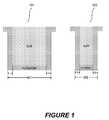
- FIG. 1shows simple cross-sectional diagrams of tungsten deposition in low and high aspect ratio features.
- FIGS. 2A-2Care simple cross-sectional diagrams illustrating deposition of tungsten in a narrow width feature using various processes.
- FIG. 3is a process flow sheet showing relevant operations of methods according to various embodiments of the present invention.
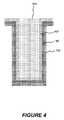
- FIG. 4is a simple cross-sectional diagram of a film stack including a titanium adhesion layer together with a tungsten nucleation layer and a tungsten bulk layer formed in accordance with this invention.
- PNLpulsed nucleation layer
- PNLpulses of the reducing agent, purge gases, and tungsten-containing precursors are sequentially injected into and purged from the reaction chamber. The process is repeated in a cyclical fashion until the desired thickness is achieved.
- PNLis similar to atomic layer deposition techniques reported in the literature. PNL is generally distinguished from atomic layer deposition (ALD) by its higher operating pressure range (greater than 1 Torr) and its higher growth rate per cycle (greater than 1 monolayer film growth per cycle).
- ALDatomic layer deposition
- PNLbroadly embodies any cyclical process of sequentially adding reactants for reaction on a semiconductor substrate. Thus, the concept embodies techniques conventionally referred to as ALD.
- a nucleation layeris a thin conformal layer which serves to facilitate the subsequent formation of a bulk material thereon.
- the nucleation layermay be formed using one or more PNL cycles. Additional discussion regarding PNL type processes can be found in the related U.S. patent application Ser. Nos. 10/435,010, 10/649,351 and 10/690,492, 11/265,531, incorporated herein by reference.
- the tungsten (W) contact or line resistanceincreases due to scattering effects in the thinner W film.
- efficient tungsten deposition processesrequire tungsten nucleation layers, these layers typically have higher electrical resistivities than the bulk tungsten layers.
- the tungsten nucleation layershould be kept as thin as possible.
- ⁇the resistivity of the material
- Lthe length of the layer in the direction of the current flow
- Athe cross-sectional area perpendicular to current flow.
- FIG. 1shows a relatively low aspect ratio feature 101 is shown in comparison to a relatively high aspect ratio feature 103 .
- These featuresare not drawn to scale but to illustrate the qualitative difference between nucleation layers in high and low aspect ratio features).
- the thickness tis the same for both features, but the width W 2 of feature 103 is much less than width W 1 of feature 101 and the nucleation layer takes up a significantly higher percentage of the total volume of the feature. As a result, the nucleation layer has a much high relative contribution to the overall resistance of the feature.
- nucleation layer thicknessfor example from a 50 A film to ⁇ 30 A
- small featuresfor example a feature having a 10:1 aspect ratio or 400 A opening
- nucleation layer thicknessfor example from a 50 A film to ⁇ 30 A
- nucleation layer thicknessfor example from a 50 A film to ⁇ 30 A
- featuresfor example a feature having a 10:1 aspect ratio or 400 A opening
- current PNL nucleation layers for standard and low resistivity W processeshas a limitation of nucleation layer thickness of around 30 A in order to obtain good step coverage and plug fill. Reducing the nucleation layer further using current processes results in degradation of the step coverage.
- Thin and uniform nucleation layersare also important for obtaining high quality, void-free tungsten deposition in narrow width and/or high aspect ratio features.
- Depositing thin nucleation layers with previous processesresulted in nucleation layers only forming on the top of the feature, without depositing a continuous nucleation layer in the bottom of the feature.
- Most tungsten fill processesfill in from the side as well at the bottom of the feature, so that when there is no nucleation layer at the bottom, CVD film cannot grow from the bottom or from the sidewall near the bottom of the feature. But the top will have some nucleation film, and CVD tungsten grows much faster on the top than the bottom sidewall due to unequal nucleation layer deposition.
- FIG. 2shows tungsten deposition in high aspect ratio features using various processes.
- tungsten depositionis shown using a low-resistivity tungsten process, which is able obtain good feature fill for aspect ratios of 10:1 or lower and features widths of above about 400 Angstroms.
- This processinvolves one or more PNL cycles at low temperature (e.g., about 300 C) to deposit the nucleation layer followed by CVD bulk deposition.
- Multiple reducing agent pulse/tungsten-precursor pulse cyclesare performed to deposit the nucleation layer.
- Hydrogenis typically run in the background and/or as a carrier gas (for the reducing agent and/or tungsten precursor) during the PNL process.
- FIG. 2Ais a rough schematic of a feature with a nucleation layer of 30 Angstroms, which contains a void. (The schematic is not shown to scale).
- FIG. 2Bshows a rough schematic of a feature with patchy nucleation layer deposition. Step coverage is very poor. Subsequent bulk deposition (now shown) is very poor with voids.
- the processes described hereinprovide very thin nucleation layers having good step coverage—optimal characteristics.
- An example of a resulting featureis shown in FIG. 2C .
- the filmsalso have lower resistivities than previously obtainable.
- the methods described hereinmay also be used in other applications to deposit ultra-thin tungsten nucleation layers having low resistivity.
- Embodiments described hereinachieve good step coverage and low resistivity W film with as little as 12 A of a nucleation layer for very aggressive features. This is compared to conventional PNL nucleation deposition processes that fail to give good step coverage and W plug fill with such thin nucleation layers.
- the bulk resistivity of the resulting PNL nucleation filmis less than that of the standard PNL process.
- the combination of lower bulk resistivity and thinner nucleation thicknessgives lower stack resistivity than the standard process. For example, for a 20 Angstrom nucleation layer, the bulk resistivity using embodiments described herein is about 50 ⁇ -cm, compared to about 75 ⁇ -cm using the standard process.
- the inventorshave recognized that running hydrogen in the background or as a carrier gas—as is conventionally done in processes such as described above with reference to FIG. 2 A—results in a higher deposition rate and thicker nucleation layer deposited. This is true even at the low temperatures used to deposit low resistivity tungsten. It is believed that in essence the reaction becomes more CVD-like, resulting in decreased step coverage. Without being bound by a particular theory it is believed that by alternating PNL boron-containing reducing agent/tungsten-containing precursor pulses without any hydrogen present, the reactants are pushed down better into high aspect ratio features.
- FIG. 3is a flow chart depicting one process flow in accordance with certain embodiments of the present invention.
- a substrateis provided and positioned in a reaction chamber as indicated by a process block 301 .
- the substrateis a partially fabricated electronic device (e.g., a partially fabricated integrated circuit). Specific applications of the invention are be described further below.
- the substratecontains a feature that has a high aspect ratio and/or narrow width.
- High aspect ratiosrange from 5:1-30:1. In certain embodiments, the aspect ratio is at least 10:1 or 20:1. Features having widths as narrow as 300-400 Angstroms also benefit from this process. In some cases, both the feature has both a high aspect ratio and a narrow width, but features having only one of these geometric characteristics benefit from the processes. For example, in one embodiment, a low resistivity tungsten layer is deposited in a feature having a width around 500 Angstrom and aspect ratio of about 30:1—a geometry at which high quality low resistivity tungsten by processes described above with reference to FIG. 2A is not possible.
- the substrateis exposed to a boron-containing reducing agent to form a boron-containing layer on the substrate surface.
- boron-containing reducing agentsare used for low-resistivity applications.
- a silanemay be used in place of the boron-containing reducing agent to achieve good step coverage in high aspect ratio and/or small features, without the benefit of the low resistivity tungsten.
- the boron-containing layeris often a layer of elemental boron, though in some embodiments, it may contain other chemical species or impurities from the boron-containing species itself or from residual gases in the reaction chamber. Any suitable boron-containing species may be used, including borane (BH 3 ), diborane (B 2 H 6 ), triborane, etc. Examples of other boron-containing species include boron halides (e.g., BF 3 , BCl 3 ) with hydrogen.
- Substrate temperatureis low—below about 35° C., for example between about 250 and 350 C or 250 and 325 C. In certain embodiments, the temperature is around 300 C.
- diboraneis provided from a diluted source (e.g., 5% diborane and 95% nitrogen). Diborane may be delivered the reaction chamber using other or additional carrier gases such as nitrogen, argon, and/or silane. Importantly, no hydrogen is used.
- the flow of boron-containing species to the reaction chamberis stopped and the reaction chamber is purged with a carrier gas such as argon, hydrogen, nitrogen or helium.
- a carrier gassuch as argon, hydrogen, nitrogen or helium.
- only argonis used at the carrier gas. The gas purge clears the regions near the substrate surface of residual gas reactants that could react with fresh gas reactants for the next reaction step.
- the next operation 305involves contacting the substrate with a tungsten-containing precursor to form a portion of the tungsten nucleation layer.
- a tungsten-containing precursormay be used.
- the tungsten-containing precursoris one of WF 6 , WCl 6 and W(CO) 6 .
- the tungsten-containing precursoris typically provided in a dilution gas, such as argon, nitrogen, or a combination thereof.
- the tungsten-containing precursoris delivered in a non-hydrogen environment.
- the substrate temperatureis low—below about 350 C, for example between about 250 and 350 C or 250 and 325 C. In certain embodiments, the temperature is around 300 C.
- Tungsten-containing precursor dosage and substrate exposure timewill vary depending upon a number factors.
- the substrateis preferably exposed until the adsorbed boron species is sufficiently consumed by reaction with the tungsten-containing precursor to produce a portion of the tungsten nucleation layer. Thereafter, the flow of tungsten-containing precursor to the reaction chamber is stopped and the reaction chamber is purged.
- the resulting portion of tungsten nucleation layer deposited in one boron-containing reducing agent/tungsten-containing precursor PNL cycleis typically about five Angstroms
- the low temperature boron-containing reducing agent pulse and tungsten precursor pulse operationsare repeated to build up the tungsten nucleation layer in an operation 307 .
- the first one or two cyclesmay not result in thickness gain due to nucleation deloay.
- the tungsten nucleation layershould be sufficiently thin so as to not unduly increase the overall tungsten film, but sufficiently thick so as to support a high quality bulk tungsten deposition.
- the process described aboveis able to deposit a tungsten nucleation layer that can support high quality bulk deposition as low as about 10 Angstroms in the high aspect ratio and/or narrow width feature.
- the thickness of the deposited nucleation layeris typically between about 10 and 30 Angstroms.
- Temperatureis one of the process conditions that affects the amount of tungsten deposited. Others include pressure, flow rate and exposure time. As discussed above, in many embodiments, maintaining temperatures at or below about 35° C. results in less material deposited during a cycle than in previously described tungsten nucleation layer deposition processes. This in turn provides lower resistivity. These PNL steps are generally performed at low temperature, e.g., below about 45° C. and in some embodiments below about 35° C., and may result in less material deposited during a cycle than in previously described tungsten nucleation layer deposition processes. In some embodiments, temperatures may be about 20° C. Because of this, for most applications of the invention, the desired thickness of the tungsten nucleation layer requires more than one PNL cycle.
- the tungsten nucleation layeris fully formed and next a bulk tungsten layer is deposited in the feature in a process operation 309 .
- the bulk tungstenis deposited using a CVD process.
- CVD processesrapidly produce low resistivity films. Any suitable CVD process may be used with any suitable tungsten-containing precursor.
- the same tungsten-containing precursor used in the PNL processes for forming the tungsten nucleation layeris use—typically one of WF 6 , WCl 6 and W(CO) 6 . Frequently, the CVD process is performed using a mixture of molecular hydrogen and one or more of these precursors.
- the CVD processmay employ a tungsten precursor together with silane or a mixture of hydrogen and silane or a mixture of hydrogen and borane (such as diborane).
- Non-CVD processcan also be employed to form the bulk layer. These include ALD/PNL and physical vapor deposition (PVD).
- the bulk tungstencan be deposited to any thickness.
- Tungsten interconnect lines for integrated circuit applicationsmay have a total thickness (tungsten nucleation layer and bulk tungsten) of between about 20 and 1,000 Angstroms.
- the total tungsten film thicknesstypically is no more than about 600 Angstroms.
- the resulting tungsten filmwill preferably have a resistivity of no greater than about 30 ⁇ -cm. Resistivity depends on how much of the total thickness is due to the nucleation layer.
- the resistivity for 500 A film (nucleation+CVD tungsten) deposited using a PNL nucleation deposition process as described with reference to FIG. 2Ais about 18 ⁇ -cm. Using the process described above with reference to FIG. 3 , the resistivity for a 500 A film is about 14 ⁇ -cm.
- the process flow of FIG. 1is complete. While the process parameters can be varied in order to influence the thickness of the nucleation layer formed at a particular cycle of the process, it has been found that depositing less material per cycle may improve step coverage, adhesion and/or resistivity. For this reason, deposition temperature is maintained at or less than about 350 C, though as discussed above, higher temperatures may also be used during the PNL deposition steps according to some embodiments.
- ultra-thin W nucleation layere.g., ⁇ 20 A
- the overall contact resistanceis improved further. Overall contact and trench line resistance may be reduced by 50%.
- the following processesare examples of processes that may be used to fill high aspect ratio features with tungsten, resulting in good gap fill and low resistivity.
- a W nucleation layerwas formed in a feature having an AR of 30:1 and a 0.15 ⁇ m opening the following pulsed nucleation layer process:
- a W bulk layerwas then formed using a CVD process (H 2 -WF 6 ) at 80 Torr and 395 C.
- the thickness of the nucleation layerwas about 80 Angstroms. Total thickness was 2000 Angstroms. Resistivity was of the film as measured on a blanket wafer was 11 ⁇ -cm. Step coverage was greater than 90%.
- a W nucleation layerwas formed in a feature having a 10:1 AR and a 0.075 ⁇ m opening using the following pulsed nucleation layer process:
- W bulk layerwas then formed using a CVD process (H 2 -WF 6 ) at 40 Torr and 395 C.
- the thickness of the nucleation layerwas about 20 Angstroms. Total thickness was 2000 Angstroms. Resistivity was of the film as measured on a blanket wafer was 11 ⁇ -cm. Step coverage was greater than 90%.
- the methods of the inventionmay be carried out in various types of deposition apparatus available from various vendors.
- suitable apparatusinclude a Novellus Concept-1 Altus, a Concept 2 Altus, a Concept-2 ALTUS-S, a Concept 3 Altus deposition system, or any of a variety of other commercially available CVD tools.
- the processcan be performed on multiple deposition stations sequentially. See, e.g., U.S. Pat. No. 6,143,082, which is incorporated herein by reference for all purposes.
- the pulsed nucleation processis performed at a first station that is one of two, five or even more deposition stations positioned within a single deposition chamber.
- the reducing gases and the tungsten-containing gasesare alternately introduced to the surface of the semiconductor substrate, at the first station, using an individual gas supply system that creates a localized atmosphere at the substrate surface.
- the waferis moved to a second deposition station and a new wafer is moved into place on the first station.
- the wafersmay be indexed from one deposition station to the next to enable parallel wafer processing after one or more repetitions of the cycle.
- the full thickness of the tungsten filmis achieved by additional cycles with alternating reducing gases and tungsten-containing gases at one or more of the other deposition stations. This is repeated until all substrates are coated to the desired thickness. It is the sum of these individual depositions that forms the total amount of tungsten nucleation layer deposited. Any number of deposition stations, each capable of having a localized atmosphere isolated from adjacent stations, is possible within the single chamber.
- the inventionalso provides for a deposition chamber in which alternating deposition stations are dedicated to deliver either tungsten-containing gases or reducing gases. More specifically, the deposition stations in the chamber are separated into two groups with the first group dedicated to delivery of the reducing gases and the second group for introducing tungsten-containing gas. These stations also can provide for the simultaneous delivery of carrier gases and/or hydrogen with the dedicated gases.
- tungstenis deposited by moving wafers from station to station such that the wafer is sequentially exposed to the reducing gases and then the tungsten-containing gases until the desired thickness of tungsten is obtained.
- the present inventionmay be used to deposit thin, low resistivity tungsten layers for many different applications.
- One preferred applicationis for interconnects in integrated circuits such as memory chips and microprocessors.
- Interconnectsare current lines found on a single metallization layer and are generally long thin flat structures. These may be formed by a blanket deposition of a tungsten layer (by a process as described above), followed by a patterning operation that defines the location of current carrying tungsten lines and removal of the tungsten from regions outside the tungsten lines.
- a primary example of an interconnect applicationis a bit line in a memory chip.
- the inventionis not limited to interconnect applications and extends to vias, contacts and other tungsten structures commonly found in electronic devices. In general, the invention finds application in any environment where thin, low-resistivity tungsten layers are required.
- the inventionis also focuses on low resistivity, tungsten layers having relatively thin proportions, typically on the order of 500 angstroms or less, preferably, 300 angstroms or less. But more generally, the invention applies to a broader range of tungsten layers, including those with thicknesses of between about 5 angstroms to 1000 angstroms.
- the roughness of the tungsten layeris not greater than about 10% of the total thickness of the deposited tungsten layer, and more preferably not greater than about 5% of the total thickness of the deposited tungsten layer.
- the roughness of a tungsten layercan be measured by various techniques such as atomic force microscopy.
- FIG. 4is a cross-section illustration of a film stack that can be formed using methods of the invention.
- the film stackmay represent interconnect applications as described previously.
- the film stack of FIG. 4is formed in an underlying substrate having a feature tungsten is to be deposited.
- the featurewhich may be a single component or more commonly a complex multi-feature structure having various conductive, insulating, and semiconductor components.
- the substratemay have a top layer comprising silicon or a dielectric such as silicon dioxide.
- Contacting the substrateis, in the following order, a titanium layer 403 , a titanium nitride layer 405 , a tungsten nucleation layer 407 (formed in accordance with this invention) and a tungsten bulk layer 409 .
- Titanium layer 403is typically deposited by a CVD process which provides reasonably good adhesion to the underlying substrate 401 .
- Titanium nitride layer 405is typically deposited using CVD or PVD methods and is used to protect the underlying titanium and/or silicon from exposure to tungsten hexafluoride (WF 6 ) during subsequent tungsten deposition. It has been found that WF 6 reacts very aggressively and sometimes explosively with titanium.
- Tungsten nucleation layer 407 and tungsten bulk layer 409are formed in accordance with the methods of the present invention as described above. In interconnect applications as described above, layers 403 , 405 , 407 and 409 are all etched to form interconnect lines. In another embodiment, a tungsten nitride layer is employed instead of the Ti/TiN layer.
Landscapes
- Chemical & Material Sciences (AREA)
- Engineering & Computer Science (AREA)
- General Chemical & Material Sciences (AREA)
- Chemical Kinetics & Catalysis (AREA)
- Physics & Mathematics (AREA)
- Manufacturing & Machinery (AREA)
- Metallurgy (AREA)
- Organic Chemistry (AREA)
- Materials Engineering (AREA)
- Condensed Matter Physics & Semiconductors (AREA)
- General Physics & Mathematics (AREA)
- Mechanical Engineering (AREA)
- Computer Hardware Design (AREA)
- Microelectronics & Electronic Packaging (AREA)
- Power Engineering (AREA)
- Electrodes Of Semiconductors (AREA)
- Chemical Vapour Deposition (AREA)
- Internal Circuitry In Semiconductor Integrated Circuit Devices (AREA)
Abstract
Description
Rtotal=Rbulk+Rnucleation=ρbulk(Lbulk/A)+ρnucleation(Lnucleation/A)
This is shown in the above simplified equation of total resistance, Rtotal, where ρ is the resistivity of the material, L is the length of the layer in the direction of the current flow and A is the cross-sectional area perpendicular to current flow. (It should be noted that contributions to the total resistance are neglected in the above equation). Because the ρnucleation>ρbulk, the thickness of the nucleation layer should be minimized to keep the total resistance as low as possible. On the other hand, the tungsten nucleation should be sufficiently thick to fully cover the underlying substrate to support high quality bulk deposition. So, to achieve an optimal thickness, the tungsten nucleation layer may be formed in one or more PNL deposition cycles.
Claims (22)
Priority Applications (4)
| Application Number | Priority Date | Filing Date | Title |
|---|---|---|---|
| US12/030,645US7955972B2 (en) | 2001-05-22 | 2008-02-13 | Methods for growing low-resistivity tungsten for high aspect ratio and small features |
| US13/095,734US8409985B2 (en) | 2001-05-22 | 2011-04-27 | Methods for growing low-resistivity tungsten for high aspect ratio and small features |
| US13/633,502US9076843B2 (en) | 2001-05-22 | 2012-10-02 | Method for producing ultra-thin tungsten layers with improved step coverage |
| US14/738,685US9583385B2 (en) | 2001-05-22 | 2015-06-12 | Method for producing ultra-thin tungsten layers with improved step coverage |
Applications Claiming Priority (7)
| Application Number | Priority Date | Filing Date | Title |
|---|---|---|---|
| US29291701P | 2001-05-22 | 2001-05-22 | |
| US09/975,074US6635965B1 (en) | 2001-05-22 | 2001-10-09 | Method for producing ultra-thin tungsten layers with improved step coverage |
| US10/649,351US7141494B2 (en) | 2001-05-22 | 2003-08-26 | Method for reducing tungsten film roughness and improving step coverage |
| US10/815,560US7262125B2 (en) | 2001-05-22 | 2004-03-31 | Method of forming low-resistivity tungsten interconnects |
| US11/265,531US7589017B2 (en) | 2001-05-22 | 2005-11-01 | Methods for growing low-resistivity tungsten film |
| US90401507P | 2007-02-27 | 2007-02-27 | |
| US12/030,645US7955972B2 (en) | 2001-05-22 | 2008-02-13 | Methods for growing low-resistivity tungsten for high aspect ratio and small features |
Related Parent Applications (1)
| Application Number | Title | Priority Date | Filing Date |
|---|---|---|---|
| US11/265,531Continuation-In-PartUS7589017B2 (en) | 2001-05-22 | 2005-11-01 | Methods for growing low-resistivity tungsten film |
Related Child Applications (1)
| Application Number | Title | Priority Date | Filing Date |
|---|---|---|---|
| US13/095,734ContinuationUS8409985B2 (en) | 2001-05-22 | 2011-04-27 | Methods for growing low-resistivity tungsten for high aspect ratio and small features |
Publications (2)
| Publication Number | Publication Date |
|---|---|
| US20080254623A1 US20080254623A1 (en) | 2008-10-16 |
| US7955972B2true US7955972B2 (en) | 2011-06-07 |
Family
ID=46330130
Family Applications (2)
| Application Number | Title | Priority Date | Filing Date |
|---|---|---|---|
| US12/030,645Expired - Fee RelatedUS7955972B2 (en) | 2001-05-22 | 2008-02-13 | Methods for growing low-resistivity tungsten for high aspect ratio and small features |
| US13/095,734Expired - Fee RelatedUS8409985B2 (en) | 2001-05-22 | 2011-04-27 | Methods for growing low-resistivity tungsten for high aspect ratio and small features |
Family Applications After (1)
| Application Number | Title | Priority Date | Filing Date |
|---|---|---|---|
| US13/095,734Expired - Fee RelatedUS8409985B2 (en) | 2001-05-22 | 2011-04-27 | Methods for growing low-resistivity tungsten for high aspect ratio and small features |
Country Status (1)
| Country | Link |
|---|---|
| US (2) | US7955972B2 (en) |
Cited By (57)
| Publication number | Priority date | Publication date | Assignee | Title |
|---|---|---|---|---|
| US20100055904A1 (en)* | 2008-08-29 | 2010-03-04 | Novellus Systems Inc. | Method for reducing tungsten roughness and improving reflectivity |
| US20100159694A1 (en)* | 2008-06-12 | 2010-06-24 | Novellus Systems Inc. | Method for depositing thin tungsten film with low resistivity and robust micro-adhesion characteristics |
| US20100267230A1 (en)* | 2009-04-16 | 2010-10-21 | Anand Chandrashekar | Method for forming tungsten contacts and interconnects with small critical dimensions |
| US20100273327A1 (en)* | 2007-12-05 | 2010-10-28 | Novellus Systems, Inc. | Method for improving uniformity and adhesion of low resistivity tungsten film |
| US20110059608A1 (en)* | 2009-09-09 | 2011-03-10 | Novellus Systems, Inc. | Method for improving adhesion of low resistivity tungsten/tungsten nitride layers |
| US20110221044A1 (en)* | 2010-03-12 | 2011-09-15 | Michal Danek | Tungsten barrier and seed for copper filled tsv |
| US8062977B1 (en) | 2008-01-31 | 2011-11-22 | Novellus Systems, Inc. | Ternary tungsten-containing resistive thin films |
| US8101521B1 (en) | 2007-07-24 | 2012-01-24 | Novellus Systems, Inc. | Methods for improving uniformity and resistivity of thin tungsten films |
| US8367546B2 (en) | 2007-12-21 | 2013-02-05 | Novellus Systems, Inc. | Methods for forming all tungsten contacts and lines |
| US20130320538A1 (en)* | 2012-05-31 | 2013-12-05 | Micron Technology, Inc. | Integrated Circuit Substrates Comprising Through-Substrate Vias And Methods Of Forming Through-Substrate Vias |
| US8853080B2 (en) | 2012-09-09 | 2014-10-07 | Novellus Systems, Inc. | Method for depositing tungsten film with low roughness and low resistivity |
| US8859417B2 (en) | 2013-01-03 | 2014-10-14 | Globalfoundries Inc. | Gate electrode(s) and contact structure(s), and methods of fabrication thereof |
| US8975184B2 (en) | 2012-07-27 | 2015-03-10 | Novellus Systems, Inc. | Methods of improving tungsten contact resistance in small critical dimension features |
| US9034760B2 (en) | 2012-06-29 | 2015-05-19 | Novellus Systems, Inc. | Methods of forming tensile tungsten films and compressive tungsten films |
| US9076843B2 (en) | 2001-05-22 | 2015-07-07 | Novellus Systems, Inc. | Method for producing ultra-thin tungsten layers with improved step coverage |
| US9082826B2 (en) | 2013-05-24 | 2015-07-14 | Lam Research Corporation | Methods and apparatuses for void-free tungsten fill in three-dimensional semiconductor features |
| US9153486B2 (en) | 2013-04-12 | 2015-10-06 | Lam Research Corporation | CVD based metal/semiconductor OHMIC contact for high volume manufacturing applications |
| US9159571B2 (en) | 2009-04-16 | 2015-10-13 | Lam Research Corporation | Tungsten deposition process using germanium-containing reducing agent |
| US9240347B2 (en) | 2012-03-27 | 2016-01-19 | Novellus Systems, Inc. | Tungsten feature fill |
| US9362163B2 (en) | 2013-07-30 | 2016-06-07 | Lam Research Corporation | Methods and apparatuses for atomic layer cleaning of contacts and vias |
| US9449921B1 (en) | 2015-12-15 | 2016-09-20 | International Business Machines Corporation | Voidless contact metal structures |
| US9548228B2 (en) | 2009-08-04 | 2017-01-17 | Lam Research Corporation | Void free tungsten fill in different sized features |
| US9589835B2 (en) | 2008-12-10 | 2017-03-07 | Novellus Systems, Inc. | Method for forming tungsten film having low resistivity, low roughness and high reflectivity |
| US9589808B2 (en) | 2013-12-19 | 2017-03-07 | Lam Research Corporation | Method for depositing extremely low resistivity tungsten |
| US9613818B2 (en) | 2015-05-27 | 2017-04-04 | Lam Research Corporation | Deposition of low fluorine tungsten by sequential CVD process |
| US9754824B2 (en) | 2015-05-27 | 2017-09-05 | Lam Research Corporation | Tungsten films having low fluorine content |
| US9953984B2 (en) | 2015-02-11 | 2018-04-24 | Lam Research Corporation | Tungsten for wordline applications |
| US9972504B2 (en) | 2015-08-07 | 2018-05-15 | Lam Research Corporation | Atomic layer etching of tungsten for enhanced tungsten deposition fill |
| US9978610B2 (en) | 2015-08-21 | 2018-05-22 | Lam Research Corporation | Pulsing RF power in etch process to enhance tungsten gapfill performance |
| US9978605B2 (en) | 2015-05-27 | 2018-05-22 | Lam Research Corporation | Method of forming low resistivity fluorine free tungsten film without nucleation |
| US9991128B2 (en) | 2016-02-05 | 2018-06-05 | Lam Research Corporation | Atomic layer etching in continuous plasma |
| US9997405B2 (en) | 2014-09-30 | 2018-06-12 | Lam Research Corporation | Feature fill with nucleation inhibition |
| US10056264B2 (en) | 2015-06-05 | 2018-08-21 | Lam Research Corporation | Atomic layer etching of GaN and other III-V materials |
| US10096487B2 (en) | 2015-08-19 | 2018-10-09 | Lam Research Corporation | Atomic layer etching of tungsten and other metals |
| US10217663B2 (en)* | 2016-02-02 | 2019-02-26 | Semiconductor Manufacturing International (Shanghai) Corporation | Apparatus for uniform metal deposition |
| US10256142B2 (en) | 2009-08-04 | 2019-04-09 | Novellus Systems, Inc. | Tungsten feature fill with nucleation inhibition |
| US10510590B2 (en) | 2017-04-10 | 2019-12-17 | Lam Research Corporation | Low resistivity films containing molybdenum |
| US10566213B2 (en) | 2016-12-19 | 2020-02-18 | Lam Research Corporation | Atomic layer etching of tantalum |
| US10566211B2 (en) | 2016-08-30 | 2020-02-18 | Lam Research Corporation | Continuous and pulsed RF plasma for etching metals |
| US10763083B2 (en) | 2017-10-06 | 2020-09-01 | Lam Research Corporation | High energy atomic layer etching |
| US20210408228A1 (en)* | 2020-06-30 | 2021-12-30 | Changxin Memory Technologies, Inc. | Semiconductor device and method for forming semiconductor device |
| US11348795B2 (en) | 2017-08-14 | 2022-05-31 | Lam Research Corporation | Metal fill process for three-dimensional vertical NAND wordline |
| US11355345B2 (en) | 2016-08-16 | 2022-06-07 | Lam Research Corporation | Method for preventing line bending during metal fill process |
| US11450513B2 (en) | 2018-03-30 | 2022-09-20 | Lam Research Corporation | Atomic layer etching and smoothing of refractory metals and other high surface binding energy materials |
| US11549175B2 (en) | 2018-05-03 | 2023-01-10 | Lam Research Corporation | Method of depositing tungsten and other metals in 3D NAND structures |
| US11821071B2 (en) | 2019-03-11 | 2023-11-21 | Lam Research Corporation | Precursors for deposition of molybdenum-containing films |
| US11970776B2 (en) | 2019-01-28 | 2024-04-30 | Lam Research Corporation | Atomic layer deposition of metal films |
| US11972952B2 (en) | 2018-12-14 | 2024-04-30 | Lam Research Corporation | Atomic layer deposition on 3D NAND structures |
| US12002679B2 (en) | 2019-04-11 | 2024-06-04 | Lam Research Corporation | High step coverage tungsten deposition |
| US12074029B2 (en) | 2018-11-19 | 2024-08-27 | Lam Research Corporation | Molybdenum deposition |
| US12077858B2 (en) | 2019-08-12 | 2024-09-03 | Lam Research Corporation | Tungsten deposition |
| US12203168B2 (en) | 2019-08-28 | 2025-01-21 | Lam Research Corporation | Metal deposition |
| US12237221B2 (en) | 2019-05-22 | 2025-02-25 | Lam Research Corporation | Nucleation-free tungsten deposition |
| US12280091B2 (en) | 2021-02-03 | 2025-04-22 | Lam Research Corporation | Etch selectivity control in atomic layer etching |
| US12327762B2 (en) | 2019-10-15 | 2025-06-10 | Lam Research Corporation | Molybdenum fill |
| US12334351B2 (en) | 2019-09-03 | 2025-06-17 | Lam Research Corporation | Molybdenum deposition |
| US12444651B2 (en) | 2022-06-28 | 2025-10-14 | Novellus Systems, Inc. | Tungsten feature fill with nucleation inhibition |
Families Citing this family (197)
| Publication number | Priority date | Publication date | Assignee | Title |
|---|---|---|---|---|
| US7955972B2 (en) | 2001-05-22 | 2011-06-07 | Novellus Systems, Inc. | Methods for growing low-resistivity tungsten for high aspect ratio and small features |
| US20100144140A1 (en)* | 2008-12-10 | 2010-06-10 | Novellus Systems, Inc. | Methods for depositing tungsten films having low resistivity for gapfill applications |
| WO2010077847A2 (en)* | 2008-12-31 | 2010-07-08 | Applied Materials, Inc. | Method of depositing tungsten film with reduced resistivity and improved surface morphology |
| US9034768B2 (en) | 2010-07-09 | 2015-05-19 | Novellus Systems, Inc. | Depositing tungsten into high aspect ratio features |
| US8124531B2 (en) | 2009-08-04 | 2012-02-28 | Novellus Systems, Inc. | Depositing tungsten into high aspect ratio features |
| US11374118B2 (en) | 2009-10-12 | 2022-06-28 | Monolithic 3D Inc. | Method to form a 3D integrated circuit |
| US10366970B2 (en) | 2009-10-12 | 2019-07-30 | Monolithic 3D Inc. | 3D semiconductor device and structure |
| US10388863B2 (en) | 2009-10-12 | 2019-08-20 | Monolithic 3D Inc. | 3D memory device and structure |
| US10043781B2 (en) | 2009-10-12 | 2018-08-07 | Monolithic 3D Inc. | 3D semiconductor device and structure |
| US11984445B2 (en) | 2009-10-12 | 2024-05-14 | Monolithic 3D Inc. | 3D semiconductor devices and structures with metal layers |
| US11018133B2 (en) | 2009-10-12 | 2021-05-25 | Monolithic 3D Inc. | 3D integrated circuit |
| US10910364B2 (en) | 2009-10-12 | 2021-02-02 | Monolitaic 3D Inc. | 3D semiconductor device |
| US10354995B2 (en) | 2009-10-12 | 2019-07-16 | Monolithic 3D Inc. | Semiconductor memory device and structure |
| US10157909B2 (en) | 2009-10-12 | 2018-12-18 | Monolithic 3D Inc. | 3D semiconductor device and structure |
| US12027518B1 (en) | 2009-10-12 | 2024-07-02 | Monolithic 3D Inc. | 3D semiconductor devices and structures with metal layers |
| US10217667B2 (en) | 2011-06-28 | 2019-02-26 | Monolithic 3D Inc. | 3D semiconductor device, fabrication method and system |
| US12362219B2 (en) | 2010-11-18 | 2025-07-15 | Monolithic 3D Inc. | 3D semiconductor memory device and structure |
| US11482440B2 (en) | 2010-12-16 | 2022-10-25 | Monolithic 3D Inc. | 3D semiconductor device and structure with a built-in test circuit for repairing faulty circuits |
| US10497713B2 (en) | 2010-11-18 | 2019-12-03 | Monolithic 3D Inc. | 3D semiconductor memory device and structure |
| US11018191B1 (en) | 2010-10-11 | 2021-05-25 | Monolithic 3D Inc. | 3D semiconductor device and structure |
| US11469271B2 (en) | 2010-10-11 | 2022-10-11 | Monolithic 3D Inc. | Method to produce 3D semiconductor devices and structures with memory |
| US11024673B1 (en) | 2010-10-11 | 2021-06-01 | Monolithic 3D Inc. | 3D semiconductor device and structure |
| US11158674B2 (en) | 2010-10-11 | 2021-10-26 | Monolithic 3D Inc. | Method to produce a 3D semiconductor device and structure |
| US11600667B1 (en) | 2010-10-11 | 2023-03-07 | Monolithic 3D Inc. | Method to produce 3D semiconductor devices and structures with memory |
| US10896931B1 (en) | 2010-10-11 | 2021-01-19 | Monolithic 3D Inc. | 3D semiconductor device and structure |
| US10290682B2 (en) | 2010-10-11 | 2019-05-14 | Monolithic 3D Inc. | 3D IC semiconductor device and structure with stacked memory |
| US11227897B2 (en) | 2010-10-11 | 2022-01-18 | Monolithic 3D Inc. | Method for producing a 3D semiconductor memory device and structure |
| US11315980B1 (en) | 2010-10-11 | 2022-04-26 | Monolithic 3D Inc. | 3D semiconductor device and structure with transistors |
| US11257867B1 (en) | 2010-10-11 | 2022-02-22 | Monolithic 3D Inc. | 3D semiconductor device and structure with oxide bonds |
| US11869915B2 (en) | 2010-10-13 | 2024-01-09 | Monolithic 3D Inc. | Multilevel semiconductor device and structure with image sensors and wafer bonding |
| US11043523B1 (en) | 2010-10-13 | 2021-06-22 | Monolithic 3D Inc. | Multilevel semiconductor device and structure with image sensors |
| US11694922B2 (en) | 2010-10-13 | 2023-07-04 | Monolithic 3D Inc. | Multilevel semiconductor device and structure with oxide bonding |
| US11437368B2 (en) | 2010-10-13 | 2022-09-06 | Monolithic 3D Inc. | Multilevel semiconductor device and structure with oxide bonding |
| US11855100B2 (en) | 2010-10-13 | 2023-12-26 | Monolithic 3D Inc. | Multilevel semiconductor device and structure with oxide bonding |
| US11063071B1 (en) | 2010-10-13 | 2021-07-13 | Monolithic 3D Inc. | Multilevel semiconductor device and structure with waveguides |
| US11855114B2 (en) | 2010-10-13 | 2023-12-26 | Monolithic 3D Inc. | Multilevel semiconductor device and structure with image sensors and wafer bonding |
| US10679977B2 (en) | 2010-10-13 | 2020-06-09 | Monolithic 3D Inc. | 3D microdisplay device and structure |
| US12080743B2 (en) | 2010-10-13 | 2024-09-03 | Monolithic 3D Inc. | Multilevel semiconductor device and structure with image sensors and wafer bonding |
| US11404466B2 (en) | 2010-10-13 | 2022-08-02 | Monolithic 3D Inc. | Multilevel semiconductor device and structure with image sensors |
| US12360310B2 (en) | 2010-10-13 | 2025-07-15 | Monolithic 3D Inc. | Multilevel semiconductor device and structure with oxide bonding |
| US10833108B2 (en) | 2010-10-13 | 2020-11-10 | Monolithic 3D Inc. | 3D microdisplay device and structure |
| US11605663B2 (en) | 2010-10-13 | 2023-03-14 | Monolithic 3D Inc. | Multilevel semiconductor device and structure with image sensors and wafer bonding |
| US11327227B2 (en) | 2010-10-13 | 2022-05-10 | Monolithic 3D Inc. | Multilevel semiconductor device and structure with electromagnetic modulators |
| US11929372B2 (en) | 2010-10-13 | 2024-03-12 | Monolithic 3D Inc. | Multilevel semiconductor device and structure with image sensors and wafer bonding |
| US11984438B2 (en) | 2010-10-13 | 2024-05-14 | Monolithic 3D Inc. | Multilevel semiconductor device and structure with oxide bonding |
| US12094892B2 (en) | 2010-10-13 | 2024-09-17 | Monolithic 3D Inc. | 3D micro display device and structure |
| US11164898B2 (en) | 2010-10-13 | 2021-11-02 | Monolithic 3D Inc. | Multilevel semiconductor device and structure |
| US11163112B2 (en) | 2010-10-13 | 2021-11-02 | Monolithic 3D Inc. | Multilevel semiconductor device and structure with electromagnetic modulators |
| US10998374B1 (en) | 2010-10-13 | 2021-05-04 | Monolithic 3D Inc. | Multilevel semiconductor device and structure |
| US10978501B1 (en) | 2010-10-13 | 2021-04-13 | Monolithic 3D Inc. | Multilevel semiconductor device and structure with waveguides |
| US10943934B2 (en) | 2010-10-13 | 2021-03-09 | Monolithic 3D Inc. | Multilevel semiconductor device and structure |
| US11133344B2 (en) | 2010-10-13 | 2021-09-28 | Monolithic 3D Inc. | Multilevel semiconductor device and structure with image sensors |
| US11901210B2 (en) | 2010-11-18 | 2024-02-13 | Monolithic 3D Inc. | 3D semiconductor device and structure with memory |
| US12033884B2 (en) | 2010-11-18 | 2024-07-09 | Monolithic 3D Inc. | Methods for producing a 3D semiconductor device and structure with memory cells and multiple metal layers |
| US11164770B1 (en) | 2010-11-18 | 2021-11-02 | Monolithic 3D Inc. | Method for producing a 3D semiconductor memory device and structure |
| US11569117B2 (en) | 2010-11-18 | 2023-01-31 | Monolithic 3D Inc. | 3D semiconductor device and structure with single-crystal layers |
| US12125737B1 (en) | 2010-11-18 | 2024-10-22 | Monolithic 3D Inc. | 3D semiconductor device and structure with metal layers and memory cells |
| US12068187B2 (en) | 2010-11-18 | 2024-08-20 | Monolithic 3D Inc. | 3D semiconductor device and structure with bonding and DRAM memory cells |
| US11482439B2 (en) | 2010-11-18 | 2022-10-25 | Monolithic 3D Inc. | Methods for producing a 3D semiconductor memory device comprising charge trap junction-less transistors |
| US11862503B2 (en) | 2010-11-18 | 2024-01-02 | Monolithic 3D Inc. | Method for producing a 3D semiconductor device and structure with memory cells and multiple metal layers |
| US12144190B2 (en) | 2010-11-18 | 2024-11-12 | Monolithic 3D Inc. | 3D semiconductor device and structure with bonding and memory cells preliminary class |
| US11018042B1 (en) | 2010-11-18 | 2021-05-25 | Monolithic 3D Inc. | 3D semiconductor memory device and structure |
| US12272586B2 (en) | 2010-11-18 | 2025-04-08 | Monolithic 3D Inc. | 3D semiconductor memory device and structure with memory and metal layers |
| US12100611B2 (en) | 2010-11-18 | 2024-09-24 | Monolithic 3D Inc. | Methods for producing a 3D semiconductor device and structure with memory cells and multiple metal layers |
| US11521888B2 (en) | 2010-11-18 | 2022-12-06 | Monolithic 3D Inc. | 3D semiconductor device and structure with high-k metal gate transistors |
| US11004719B1 (en) | 2010-11-18 | 2021-05-11 | Monolithic 3D Inc. | Methods for producing a 3D semiconductor memory device and structure |
| US11094576B1 (en) | 2010-11-18 | 2021-08-17 | Monolithic 3D Inc. | Methods for producing a 3D semiconductor memory device and structure |
| US11443971B2 (en) | 2010-11-18 | 2022-09-13 | Monolithic 3D Inc. | 3D semiconductor device and structure with memory |
| US11508605B2 (en) | 2010-11-18 | 2022-11-22 | Monolithic 3D Inc. | 3D semiconductor memory device and structure |
| US11923230B1 (en) | 2010-11-18 | 2024-03-05 | Monolithic 3D Inc. | 3D semiconductor device and structure with bonding |
| US11107721B2 (en) | 2010-11-18 | 2021-08-31 | Monolithic 3D Inc. | 3D semiconductor device and structure with NAND logic |
| US11784082B2 (en) | 2010-11-18 | 2023-10-10 | Monolithic 3D Inc. | 3D semiconductor device and structure with bonding |
| US11482438B2 (en) | 2010-11-18 | 2022-10-25 | Monolithic 3D Inc. | Methods for producing a 3D semiconductor memory device and structure |
| US11211279B2 (en) | 2010-11-18 | 2021-12-28 | Monolithic 3D Inc. | Method for processing a 3D integrated circuit and structure |
| US11615977B2 (en) | 2010-11-18 | 2023-03-28 | Monolithic 3D Inc. | 3D semiconductor memory device and structure |
| US11804396B2 (en) | 2010-11-18 | 2023-10-31 | Monolithic 3D Inc. | Methods for producing a 3D semiconductor device and structure with memory cells and multiple metal layers |
| US11854857B1 (en) | 2010-11-18 | 2023-12-26 | Monolithic 3D Inc. | Methods for producing a 3D semiconductor device and structure with memory cells and multiple metal layers |
| US11495484B2 (en) | 2010-11-18 | 2022-11-08 | Monolithic 3D Inc. | 3D semiconductor devices and structures with at least two single-crystal layers |
| US11355381B2 (en) | 2010-11-18 | 2022-06-07 | Monolithic 3D Inc. | 3D semiconductor memory device and structure |
| US11031275B2 (en) | 2010-11-18 | 2021-06-08 | Monolithic 3D Inc. | 3D semiconductor device and structure with memory |
| US11610802B2 (en) | 2010-11-18 | 2023-03-21 | Monolithic 3D Inc. | Method for producing a 3D semiconductor device and structure with single crystal transistors and metal gate electrodes |
| US12136562B2 (en) | 2010-11-18 | 2024-11-05 | Monolithic 3D Inc. | 3D semiconductor device and structure with single-crystal layers |
| US12154817B1 (en) | 2010-11-18 | 2024-11-26 | Monolithic 3D Inc. | Methods for producing a 3D semiconductor memory device and structure |
| US12243765B2 (en) | 2010-11-18 | 2025-03-04 | Monolithic 3D Inc. | 3D semiconductor device and structure with metal layers and memory cells |
| US11735462B2 (en) | 2010-11-18 | 2023-08-22 | Monolithic 3D Inc. | 3D semiconductor device and structure with single-crystal layers |
| US11355380B2 (en) | 2010-11-18 | 2022-06-07 | Monolithic 3D Inc. | Methods for producing 3D semiconductor memory device and structure utilizing alignment marks |
| US11121021B2 (en) | 2010-11-18 | 2021-09-14 | Monolithic 3D Inc. | 3D semiconductor device and structure |
| US10388568B2 (en) | 2011-06-28 | 2019-08-20 | Monolithic 3D Inc. | 3D semiconductor device and system |
| US8883637B2 (en) | 2011-06-30 | 2014-11-11 | Novellus Systems, Inc. | Systems and methods for controlling etch selectivity of various materials |
| US20130224948A1 (en)* | 2012-02-28 | 2013-08-29 | Globalfoundries Inc. | Methods for deposition of tungsten in the fabrication of an integrated circuit |
| US10381266B2 (en) | 2012-03-27 | 2019-08-13 | Novellus Systems, Inc. | Tungsten feature fill with nucleation inhibition |
| US11437269B2 (en) | 2012-03-27 | 2022-09-06 | Novellus Systems, Inc. | Tungsten feature fill with nucleation inhibition |
| US11476181B1 (en) | 2012-04-09 | 2022-10-18 | Monolithic 3D Inc. | 3D semiconductor device and structure with metal layers |
| US11594473B2 (en) | 2012-04-09 | 2023-02-28 | Monolithic 3D Inc. | 3D semiconductor device and structure with metal layers and a connective path |
| US11410912B2 (en) | 2012-04-09 | 2022-08-09 | Monolithic 3D Inc. | 3D semiconductor device with vias and isolation layers |
| US11694944B1 (en) | 2012-04-09 | 2023-07-04 | Monolithic 3D Inc. | 3D semiconductor device and structure with metal layers and a connective path |
| US10600888B2 (en) | 2012-04-09 | 2020-03-24 | Monolithic 3D Inc. | 3D semiconductor device |
| US11881443B2 (en) | 2012-04-09 | 2024-01-23 | Monolithic 3D Inc. | 3D semiconductor device and structure with metal layers and a connective path |
| US11164811B2 (en) | 2012-04-09 | 2021-11-02 | Monolithic 3D Inc. | 3D semiconductor device with isolation layers and oxide-to-oxide bonding |
| US11088050B2 (en) | 2012-04-09 | 2021-08-10 | Monolithic 3D Inc. | 3D semiconductor device with isolation layers |
| US11616004B1 (en) | 2012-04-09 | 2023-03-28 | Monolithic 3D Inc. | 3D semiconductor device and structure with metal layers and a connective path |
| US11735501B1 (en) | 2012-04-09 | 2023-08-22 | Monolithic 3D Inc. | 3D semiconductor device and structure with metal layers and a connective path |
| US11217565B2 (en) | 2012-12-22 | 2022-01-04 | Monolithic 3D Inc. | Method to form a 3D semiconductor device and structure |
| US12051674B2 (en) | 2012-12-22 | 2024-07-30 | Monolithic 3D Inc. | 3D semiconductor device and structure with metal layers |
| US11916045B2 (en) | 2012-12-22 | 2024-02-27 | Monolithic 3D Inc. | 3D semiconductor device and structure with metal layers |
| US11961827B1 (en) | 2012-12-22 | 2024-04-16 | Monolithic 3D Inc. | 3D semiconductor device and structure with metal layers |
| US11063024B1 (en) | 2012-12-22 | 2021-07-13 | Monlithic 3D Inc. | Method to form a 3D semiconductor device and structure |
| US11018116B2 (en) | 2012-12-22 | 2021-05-25 | Monolithic 3D Inc. | Method to form a 3D semiconductor device and structure |
| US11784169B2 (en) | 2012-12-22 | 2023-10-10 | Monolithic 3D Inc. | 3D semiconductor device and structure with metal layers |
| US11309292B2 (en) | 2012-12-22 | 2022-04-19 | Monolithic 3D Inc. | 3D semiconductor device and structure with metal layers |
| US11967583B2 (en) | 2012-12-22 | 2024-04-23 | Monolithic 3D Inc. | 3D semiconductor device and structure with metal layers |
| US11177140B2 (en) | 2012-12-29 | 2021-11-16 | Monolithic 3D Inc. | 3D semiconductor device and structure |
| US10115663B2 (en) | 2012-12-29 | 2018-10-30 | Monolithic 3D Inc. | 3D semiconductor device and structure |
| US10600657B2 (en) | 2012-12-29 | 2020-03-24 | Monolithic 3D Inc | 3D semiconductor device and structure |
| US10903089B1 (en) | 2012-12-29 | 2021-01-26 | Monolithic 3D Inc. | 3D semiconductor device and structure |
| US12249538B2 (en) | 2012-12-29 | 2025-03-11 | Monolithic 3D Inc. | 3D semiconductor device and structure including power distribution grids |
| US11430668B2 (en) | 2012-12-29 | 2022-08-30 | Monolithic 3D Inc. | 3D semiconductor device and structure with bonding |
| US11430667B2 (en) | 2012-12-29 | 2022-08-30 | Monolithic 3D Inc. | 3D semiconductor device and structure with bonding |
| US10892169B2 (en) | 2012-12-29 | 2021-01-12 | Monolithic 3D Inc. | 3D semiconductor device and structure |
| US11087995B1 (en) | 2012-12-29 | 2021-08-10 | Monolithic 3D Inc. | 3D semiconductor device and structure |
| US11004694B1 (en) | 2012-12-29 | 2021-05-11 | Monolithic 3D Inc. | 3D semiconductor device and structure |
| US10651054B2 (en) | 2012-12-29 | 2020-05-12 | Monolithic 3D Inc. | 3D semiconductor device and structure |
| US12094965B2 (en) | 2013-03-11 | 2024-09-17 | Monolithic 3D Inc. | 3D semiconductor device and structure with metal layers and memory cells |
| US10325651B2 (en) | 2013-03-11 | 2019-06-18 | Monolithic 3D Inc. | 3D semiconductor device with stacked memory |
| US8902663B1 (en) | 2013-03-11 | 2014-12-02 | Monolithic 3D Inc. | Method of maintaining a memory state |
| US11869965B2 (en) | 2013-03-11 | 2024-01-09 | Monolithic 3D Inc. | 3D semiconductor device and structure with metal layers and memory cells |
| US11935949B1 (en) | 2013-03-11 | 2024-03-19 | Monolithic 3D Inc. | 3D semiconductor device and structure with metal layers and memory cells |
| US11088130B2 (en) | 2014-01-28 | 2021-08-10 | Monolithic 3D Inc. | 3D semiconductor device and structure |
| US11923374B2 (en) | 2013-03-12 | 2024-03-05 | Monolithic 3D Inc. | 3D semiconductor device and structure with metal layers |
| US10840239B2 (en) | 2014-08-26 | 2020-11-17 | Monolithic 3D Inc. | 3D semiconductor device and structure |
| US12100646B2 (en) | 2013-03-12 | 2024-09-24 | Monolithic 3D Inc. | 3D semiconductor device and structure with metal layers |
| US11398569B2 (en) | 2013-03-12 | 2022-07-26 | Monolithic 3D Inc. | 3D semiconductor device and structure |
| US10224279B2 (en) | 2013-03-15 | 2019-03-05 | Monolithic 3D Inc. | Semiconductor device and structure |
| US11487928B2 (en) | 2013-04-15 | 2022-11-01 | Monolithic 3D Inc. | Automation for monolithic 3D devices |
| US11574109B1 (en) | 2013-04-15 | 2023-02-07 | Monolithic 3D Inc | Automation methods for 3D integrated circuits and devices |
| US11720736B2 (en) | 2013-04-15 | 2023-08-08 | Monolithic 3D Inc. | Automation methods for 3D integrated circuits and devices |
| US11270055B1 (en) | 2013-04-15 | 2022-03-08 | Monolithic 3D Inc. | Automation for monolithic 3D devices |
| US9021414B1 (en) | 2013-04-15 | 2015-04-28 | Monolithic 3D Inc. | Automation for monolithic 3D devices |
| US11341309B1 (en) | 2013-04-15 | 2022-05-24 | Monolithic 3D Inc. | Automation for monolithic 3D devices |
| US11030371B2 (en) | 2013-04-15 | 2021-06-08 | Monolithic 3D Inc. | Automation for monolithic 3D devices |
| US20150111374A1 (en)* | 2013-10-18 | 2015-04-23 | International Business Machines Corporation | Surface treatment in a dep-etch-dep process |
| TWI672737B (en)* | 2013-12-27 | 2019-09-21 | 美商蘭姆研究公司 | Tungsten nucleation process to enable low resistivity tungsten feature fill |
| US11031394B1 (en) | 2014-01-28 | 2021-06-08 | Monolithic 3D Inc. | 3D semiconductor device and structure |
| US11107808B1 (en) | 2014-01-28 | 2021-08-31 | Monolithic 3D Inc. | 3D semiconductor device and structure |
| US12094829B2 (en) | 2014-01-28 | 2024-09-17 | Monolithic 3D Inc. | 3D semiconductor device and structure |
| US10297586B2 (en) | 2015-03-09 | 2019-05-21 | Monolithic 3D Inc. | Methods for processing a 3D semiconductor device |
| US9748137B2 (en) | 2014-08-21 | 2017-08-29 | Lam Research Corporation | Method for void-free cobalt gap fill |
| US11056468B1 (en) | 2015-04-19 | 2021-07-06 | Monolithic 3D Inc. | 3D semiconductor device and structure |
| US10825779B2 (en) | 2015-04-19 | 2020-11-03 | Monolithic 3D Inc. | 3D semiconductor device and structure |
| US10381328B2 (en) | 2015-04-19 | 2019-08-13 | Monolithic 3D Inc. | Semiconductor device and structure |
| US11011507B1 (en) | 2015-04-19 | 2021-05-18 | Monolithic 3D Inc. | 3D semiconductor device and structure |
| US10170320B2 (en) | 2015-05-18 | 2019-01-01 | Lam Research Corporation | Feature fill with multi-stage nucleation inhibition |
| US11956952B2 (en) | 2015-08-23 | 2024-04-09 | Monolithic 3D Inc. | Semiconductor memory device and structure |
| US11978731B2 (en) | 2015-09-21 | 2024-05-07 | Monolithic 3D Inc. | Method to produce a multi-level semiconductor memory device and structure |
| US12100658B2 (en) | 2015-09-21 | 2024-09-24 | Monolithic 3D Inc. | Method to produce a 3D multilayer semiconductor device and structure |
| US12250830B2 (en) | 2015-09-21 | 2025-03-11 | Monolithic 3D Inc. | 3D semiconductor memory devices and structures |
| US11114427B2 (en) | 2015-11-07 | 2021-09-07 | Monolithic 3D Inc. | 3D semiconductor processor and memory device and structure |
| US11937422B2 (en) | 2015-11-07 | 2024-03-19 | Monolithic 3D Inc. | Semiconductor memory device and structure |
| CN108401468A (en) | 2015-09-21 | 2018-08-14 | 莫诺利特斯3D有限公司 | 3D semiconductor devices and structures |
| US12178055B2 (en) | 2015-09-21 | 2024-12-24 | Monolithic 3D Inc. | 3D semiconductor memory devices and structures |
| US10522225B1 (en) | 2015-10-02 | 2019-12-31 | Monolithic 3D Inc. | Semiconductor device with non-volatile memory |
| US10418369B2 (en) | 2015-10-24 | 2019-09-17 | Monolithic 3D Inc. | Multi-level semiconductor memory device and structure |
| US10847540B2 (en) | 2015-10-24 | 2020-11-24 | Monolithic 3D Inc. | 3D semiconductor memory device and structure |
| US11991884B1 (en) | 2015-10-24 | 2024-05-21 | Monolithic 3D Inc. | 3D semiconductor device and structure with logic and memory |
| US12219769B2 (en) | 2015-10-24 | 2025-02-04 | Monolithic 3D Inc. | 3D semiconductor device and structure with logic and memory |
| US11296115B1 (en) | 2015-10-24 | 2022-04-05 | Monolithic 3D Inc. | 3D semiconductor device and structure |
| US12035531B2 (en) | 2015-10-24 | 2024-07-09 | Monolithic 3D Inc. | 3D semiconductor device and structure with logic and memory |
| US11114464B2 (en) | 2015-10-24 | 2021-09-07 | Monolithic 3D Inc. | 3D semiconductor device and structure |
| US12016181B2 (en) | 2015-10-24 | 2024-06-18 | Monolithic 3D Inc. | 3D semiconductor device and structure with logic and memory |
| US12120880B1 (en) | 2015-10-24 | 2024-10-15 | Monolithic 3D Inc. | 3D semiconductor device and structure with logic and memory |
| US10468263B2 (en) | 2015-12-19 | 2019-11-05 | Applied Materials, Inc. | Tungsten deposition without barrier layer |
| US10991586B2 (en) | 2015-12-19 | 2021-04-27 | Applied Materials, Inc. | In-situ tungsten deposition without barrier layer |
| US11329059B1 (en) | 2016-10-10 | 2022-05-10 | Monolithic 3D Inc. | 3D memory devices and structures with thinned single crystal substrates |
| US11251149B2 (en) | 2016-10-10 | 2022-02-15 | Monolithic 3D Inc. | 3D memory device and structure |
| US11869591B2 (en) | 2016-10-10 | 2024-01-09 | Monolithic 3D Inc. | 3D memory devices and structures with control circuits |
| US11711928B2 (en) | 2016-10-10 | 2023-07-25 | Monolithic 3D Inc. | 3D memory devices and structures with control circuits |
| US11812620B2 (en) | 2016-10-10 | 2023-11-07 | Monolithic 3D Inc. | 3D DRAM memory devices and structures with control circuits |
| US11930648B1 (en) | 2016-10-10 | 2024-03-12 | Monolithic 3D Inc. | 3D memory devices and structures with metal layers |
| US12225704B2 (en) | 2016-10-10 | 2025-02-11 | Monolithic 3D Inc. | 3D memory devices and structures with memory arrays and metal layers |
| US10211099B2 (en) | 2016-12-19 | 2019-02-19 | Lam Research Corporation | Chamber conditioning for remote plasma process |
| SG11202009514WA (en)* | 2018-04-24 | 2020-11-27 | Applied Materials Inc | Tungsten deposition without barrier layer |
| WO2019209289A1 (en)* | 2018-04-25 | 2019-10-31 | Entegris, Inc. | Low temperature molybdenum film depositon utilizing boron nucleation layers |
| US20210140043A1 (en)* | 2018-07-26 | 2021-05-13 | Lam Research Corporation | Deposition of pure metal films |
| CN110880489B (en)* | 2018-09-05 | 2025-04-04 | 长鑫存储技术有限公司 | Semiconductor interconnect structure and method for manufacturing the same |
| US10930493B2 (en)* | 2018-10-29 | 2021-02-23 | Applied Materials, Inc. | Linerless continuous amorphous metal films |
| JP7705347B2 (en) | 2018-12-05 | 2025-07-09 | ラム リサーチ コーポレーション | Void-free, low stress filling |
| JP7705349B2 (en) | 2019-02-13 | 2025-07-09 | ラム リサーチ コーポレーション | Tungsten feature filling with inhibition control |
| US10892016B1 (en) | 2019-04-08 | 2021-01-12 | Monolithic 3D Inc. | 3D memory semiconductor devices and structures |
| US11018156B2 (en) | 2019-04-08 | 2021-05-25 | Monolithic 3D Inc. | 3D memory semiconductor devices and structures |
| US11158652B1 (en) | 2019-04-08 | 2021-10-26 | Monolithic 3D Inc. | 3D memory semiconductor devices and structures |
| US11763864B2 (en) | 2019-04-08 | 2023-09-19 | Monolithic 3D Inc. | 3D memory semiconductor devices and structures with bit-line pillars |
| US11296106B2 (en) | 2019-04-08 | 2022-04-05 | Monolithic 3D Inc. | 3D memory semiconductor devices and structures |
| US20210125862A1 (en)* | 2019-10-25 | 2021-04-29 | Qualcomm Incorporated | Super via integration in integrated circuits |
| CN113871344B (en)* | 2020-06-30 | 2025-03-28 | 长鑫存储技术有限公司 | Semiconductor device and method for forming semiconductor device |
| US11377733B2 (en)* | 2020-08-07 | 2022-07-05 | Sandisk Technologies Llc | Fluorine-free tungsten deposition process employing in-situ oxidation and apparatuses for effecting the same |
| US12037682B2 (en)* | 2021-10-05 | 2024-07-16 | Applied Materials, Inc. | Methods for forming low resistivity tungsten features |
| CN119522482A (en)* | 2022-06-30 | 2025-02-25 | 应用材料公司 | Plasma-enhanced tungsten nucleation at low resistivity |
Citations (64)
| Publication number | Priority date | Publication date | Assignee | Title |
|---|---|---|---|---|
| US4746375A (en) | 1987-05-08 | 1988-05-24 | General Electric Company | Activation of refractory metal surfaces for electroless plating |
| US4804560A (en) | 1986-03-17 | 1989-02-14 | Fujitsu Limited | Method of selectively depositing tungsten upon a semiconductor substrate |
| US5028565A (en) | 1989-08-25 | 1991-07-02 | Applied Materials, Inc. | Process for CVD deposition of tungsten layer on semiconductor wafer |
| US5227329A (en) | 1990-08-31 | 1993-07-13 | Hitachi, Ltd. | Method of manufacturing semiconductor device |
| US5250329A (en) | 1989-04-06 | 1993-10-05 | Microelectronics And Computer Technology Corporation | Method of depositing conductive lines on a dielectric |
| US5326723A (en) | 1992-09-09 | 1994-07-05 | Intel Corporation | Method for improving stability of tungsten chemical vapor deposition |
| US5391394A (en) | 1990-01-08 | 1995-02-21 | Lsi Logic Corporation | Tungsten deposition process for low contact resistivity to silicon |
| US5661080A (en) | 1992-12-10 | 1997-08-26 | Hyundai Electronics Industries Co., Ltd. | Method for fabricating tungsten plug |
| US5726096A (en) | 1993-12-17 | 1998-03-10 | Hyundai Electronics Industries Co., Ltd. | Method for forming a tungsten silicide layer in a semiconductor device |
| US5795824A (en) | 1997-08-28 | 1998-08-18 | Novellus Systems, Inc. | Method for nucleation of CVD tungsten films |
| US5804249A (en) | 1997-02-07 | 1998-09-08 | Lsi Logic Corporation | Multistep tungsten CVD process with amorphization step |
| US5817576A (en) | 1994-09-27 | 1998-10-06 | Applied Materials, Inc. | Utilization of SiH4 soak and purge in deposition processes |
| US5926720A (en)* | 1997-09-08 | 1999-07-20 | Lsi Logic Corporation | Consistent alignment mark profiles on semiconductor wafers using PVD shadowing |
| US5956609A (en) | 1997-08-11 | 1999-09-21 | Taiwan Semiconductor Manufacturing Company, Ltd. | Method for reducing stress and improving step-coverage of tungsten interconnects and plugs |
| US6001729A (en) | 1995-01-10 | 1999-12-14 | Kawasaki Steel Corporation | Method of forming wiring structure for semiconductor device |
| US6017818A (en) | 1996-01-22 | 2000-01-25 | Texas Instruments Incorporated | Process for fabricating conformal Ti-Si-N and Ti-B-N based barrier films with low defect density |
| US6037263A (en) | 1998-11-05 | 2000-03-14 | Vanguard International Semiconductor Corporation | Plasma enhanced CVD deposition of tungsten and tungsten compounds |
| US6066366A (en) | 1998-07-22 | 2000-05-23 | Applied Materials, Inc. | Method for depositing uniform tungsten layers by CVD |
| US6099904A (en) | 1997-12-02 | 2000-08-08 | Applied Materials, Inc. | Low resistivity W using B2 H6 nucleation step |
| US6107200A (en) | 1998-03-12 | 2000-08-22 | Fujitsu Limited | Semiconductor device manufacturing method |
| US6143082A (en) | 1998-10-08 | 2000-11-07 | Novellus Systems, Inc. | Isolation of incompatible processes in a multi-station processing chamber |
| US6174812B1 (en) | 1999-06-08 | 2001-01-16 | United Microelectronics Corp. | Copper damascene technology for ultra large scale integration circuits |
| WO2001027347A1 (en) | 1999-10-15 | 2001-04-19 | Asm Microchemistry Oy | Method of depositing transition metal nitride thin films |
| US6245654B1 (en) | 1999-03-31 | 2001-06-12 | Taiwan Semiconductor Manufacturing Company, Ltd | Method for preventing tungsten contact/via plug loss after a backside pressure fault |
| US20010008808A1 (en) | 1995-10-25 | 2001-07-19 | Fernando Gonzalez | A Method Of Fabricating A DRAM Transistor With A Dual Gate Oxide Technique |
| US6265312B1 (en) | 1999-08-02 | 2001-07-24 | Stmicroelectronics, Inc. | Method for depositing an integrated circuit tungsten film stack that includes a post-nucleation pump down step |
| US20010014533A1 (en) | 1999-01-08 | 2001-08-16 | Shih-Wei Sun | Method of fabricating salicide |
| US6277744B1 (en) | 2000-01-21 | 2001-08-21 | Advanced Micro Devices, Inc. | Two-level silane nucleation for blanket tungsten deposition |
| US20010015494A1 (en) | 1997-06-13 | 2001-08-23 | Kie Y. Ahn | Integrated circuit wiring with low rc time delay |
| US6294468B1 (en) | 1999-05-24 | 2001-09-25 | Agere Systems Guardian Corp. | Method of chemical vapor depositing tungsten films |
| US6297152B1 (en) | 1996-12-12 | 2001-10-02 | Applied Materials, Inc. | CVD process for DCS-based tungsten silicide |
| US6309966B1 (en) | 1999-09-03 | 2001-10-30 | Motorola, Inc. | Apparatus and method of a low pressure, two-step nucleation tungsten deposition |
| US20010044041A1 (en) | 2000-05-18 | 2001-11-22 | Badding Michael E. | High performance solid electrolyte fuel cells |
| US6355558B1 (en) | 1999-06-10 | 2002-03-12 | Texas Instruments Incorporated | Metallization structure, and associated method, to improve crystallographic texture and cavity fill for CVD aluminum/PVD aluminum alloy films |
| US6404054B1 (en) | 1998-10-28 | 2002-06-11 | Samsung Electronics Co., Ltd. | Tungsten layer formation method for semiconductor device and semiconductor device using the same |
| US20020090796A1 (en) | 1999-09-13 | 2002-07-11 | Applied Materials, Inc. | Silicon layer to improve plug filling by CVD |
| US20020177316A1 (en) | 2000-11-16 | 2002-11-28 | Miller Anne E. | Slurry and method for chemical mechanical polishing of copper |
| US20030059980A1 (en) | 2001-09-25 | 2003-03-27 | Ling Chen | Copper interconnect barrier layer structure and formation method |
| US6551929B1 (en) | 2000-06-28 | 2003-04-22 | Applied Materials, Inc. | Bifurcated deposition process for depositing refractory metal layers employing atomic layer deposition and chemical vapor deposition techniques |
| US6566250B1 (en) | 2002-03-18 | 2003-05-20 | Taiwant Semiconductor Manufacturing Co., Ltd | Method for forming a self aligned capping layer |
| US6566262B1 (en) | 2001-11-01 | 2003-05-20 | Lsi Logic Corporation | Method for creating self-aligned alloy capping layers for copper interconnect structures |
| US20030104126A1 (en) | 2001-10-10 | 2003-06-05 | Hongbin Fang | Method for depositing refractory metal layers employing sequential deposition techniques |
| US20030127043A1 (en) | 2001-07-13 | 2003-07-10 | Applied Materials, Inc. | Pulsed nucleation deposition of tungsten layers |
| US6635965B1 (en) | 2001-05-22 | 2003-10-21 | Novellus Systems, Inc. | Method for producing ultra-thin tungsten layers with improved step coverage |
| US20040014315A1 (en) | 2001-07-16 | 2004-01-22 | Applied Materials, Inc. | Formation of composite tungsten films |
| US20040044127A1 (en) | 2002-08-22 | 2004-03-04 | Konica Corporation | Organic-inorganic hybrid film, its manufacturing method, optical film, and polarizing film |
| US6706625B1 (en) | 2002-12-06 | 2004-03-16 | Chartered Semiconductor Manufacturing Ltd. | Copper recess formation using chemical process for fabricating barrier cap for lines and vias |
| US6720261B1 (en) | 1999-06-02 | 2004-04-13 | Agere Systems Inc. | Method and system for eliminating extrusions in semiconductor vias |
| US6740585B2 (en) | 2001-07-25 | 2004-05-25 | Applied Materials, Inc. | Barrier formation using novel sputter deposition method with PVD, CVD, or ALD |
| US20040202786A1 (en) | 2001-05-22 | 2004-10-14 | Novellus Systems, Inc. | Method of forming low-resistivity tungsten interconnects |
| US20040206267A1 (en) | 2002-12-23 | 2004-10-21 | Sankar Sambasivan | Aluminum phosphate coatings |
| US6844258B1 (en) | 2003-05-09 | 2005-01-18 | Novellus Systems, Inc. | Selective refractory metal and nitride capping |
| US20050031786A1 (en) | 2001-05-22 | 2005-02-10 | Novellus Systems, Inc. | Method for reducing tungsten film roughness and improving step coverage |
| US6861356B2 (en) | 1997-11-05 | 2005-03-01 | Tokyo Electron Limited | Method of forming a barrier film and method of forming wiring structure and electrodes of semiconductor device having a barrier film |
| US6902763B1 (en) | 1999-10-15 | 2005-06-07 | Asm International N.V. | Method for depositing nanolaminate thin films on sensitive surfaces |
| US20050136594A1 (en) | 2003-12-23 | 2005-06-23 | Hynix Semiconductor Inc. | Method for forming bit-line of semiconductor device |
| US6936538B2 (en)* | 2001-07-16 | 2005-08-30 | Applied Materials, Inc. | Method and apparatus for depositing tungsten after surface treatment to improve film characteristics |
| US6962873B1 (en) | 2002-12-10 | 2005-11-08 | Novellus Systems, Inc. | Nitridation of electrolessly deposited cobalt |
| US7005372B2 (en) | 2003-01-21 | 2006-02-28 | Novellus Systems, Inc. | Deposition of tungsten nitride |
| US20080124926A1 (en) | 2001-05-22 | 2008-05-29 | Novellus Systems, Inc. | Methods for growing low-resistivity tungsten film |
| US7429402B2 (en)* | 2004-12-10 | 2008-09-30 | Applied Materials, Inc. | Ruthenium as an underlayer for tungsten film deposition |
| US20090149022A1 (en) | 2007-12-05 | 2009-06-11 | Novellus Systems, Inc. | Method for improving uniformity and adhesion of low resistivity tungsten film |
| US7655567B1 (en) | 2007-07-24 | 2010-02-02 | Novellus Systems, Inc. | Methods for improving uniformity and resistivity of thin tungsten films |
| US7754604B2 (en) | 2003-08-26 | 2010-07-13 | Novellus Systems, Inc. | Reducing silicon attack and improving resistivity of tungsten nitride film |
Family Cites Families (24)
| Publication number | Priority date | Publication date | Assignee | Title |
|---|---|---|---|---|
| JPS62260340A (en)* | 1986-05-06 | 1987-11-12 | Toshiba Corp | Manufacturing method of semiconductor device |
| US6331483B1 (en)* | 1998-12-18 | 2001-12-18 | Tokyo Electron Limited | Method of film-forming of tungsten |
| US6429126B1 (en)* | 2000-03-29 | 2002-08-06 | Applied Materials, Inc. | Reduced fluorine contamination for tungsten CVD |
| US7405158B2 (en) | 2000-06-28 | 2008-07-29 | Applied Materials, Inc. | Methods for depositing tungsten layers employing atomic layer deposition techniques |
| US6908848B2 (en)* | 2000-12-20 | 2005-06-21 | Samsung Electronics, Co., Ltd. | Method for forming an electrical interconnection providing improved surface morphology of tungsten |
| US7955972B2 (en) | 2001-05-22 | 2011-06-07 | Novellus Systems, Inc. | Methods for growing low-resistivity tungsten for high aspect ratio and small features |
| JP2005504885A (en)* | 2001-07-25 | 2005-02-17 | アプライド マテリアルズ インコーポレイテッド | Barrier formation using a novel sputter deposition method |
| US6905543B1 (en)* | 2002-06-19 | 2005-06-14 | Novellus Systems, Inc | Methods of forming tungsten nucleation layer |
| US7211508B2 (en)* | 2003-06-18 | 2007-05-01 | Applied Materials, Inc. | Atomic layer deposition of tantalum based barrier materials |
| JP4606006B2 (en)* | 2003-09-11 | 2011-01-05 | ルネサスエレクトロニクス株式会社 | Manufacturing method of semiconductor device |
| US7605469B2 (en)* | 2004-06-30 | 2009-10-20 | Intel Corporation | Atomic layer deposited tantalum containing adhesion layer |
| US7220671B2 (en)* | 2005-03-31 | 2007-05-22 | Intel Corporation | Organometallic precursors for the chemical phase deposition of metal films in interconnect applications |
| US7524765B2 (en)* | 2005-11-02 | 2009-04-28 | Intel Corporation | Direct tailoring of the composition and density of ALD films |
| US8153831B2 (en)* | 2006-09-28 | 2012-04-10 | Praxair Technology, Inc. | Organometallic compounds, processes for the preparation thereof and methods of use thereof |
| US8053365B2 (en)* | 2007-12-21 | 2011-11-08 | Novellus Systems, Inc. | Methods for forming all tungsten contacts and lines |
| US8062977B1 (en) | 2008-01-31 | 2011-11-22 | Novellus Systems, Inc. | Ternary tungsten-containing resistive thin films |
| US8058170B2 (en)* | 2008-06-12 | 2011-11-15 | Novellus Systems, Inc. | Method for depositing thin tungsten film with low resistivity and robust micro-adhesion characteristics |
| US8551885B2 (en) | 2008-08-29 | 2013-10-08 | Novellus Systems, Inc. | Method for reducing tungsten roughness and improving reflectivity |
| JP2010180303A (en)* | 2009-02-04 | 2010-08-19 | Sumitomo Chemical Co Ltd | Hydrophilizing agent, method of producing the same, and use of the same |
| US20100267230A1 (en)* | 2009-04-16 | 2010-10-21 | Anand Chandrashekar | Method for forming tungsten contacts and interconnects with small critical dimensions |
| US8207062B2 (en)* | 2009-09-09 | 2012-06-26 | Novellus Systems, Inc. | Method for improving adhesion of low resistivity tungsten/tungsten nitride layers |
| DE102009055392B4 (en)* | 2009-12-30 | 2014-05-22 | Globalfoundries Dresden Module One Limited Liability Company & Co. Kg | Semiconductor component and method for producing the semiconductor device |
| US8709948B2 (en)* | 2010-03-12 | 2014-04-29 | Novellus Systems, Inc. | Tungsten barrier and seed for copper filled TSV |
| US20120199887A1 (en) | 2011-02-03 | 2012-08-09 | Lana Chan | Methods of controlling tungsten film properties |
- 2008
- 2008-02-13USUS12/030,645patent/US7955972B2/ennot_activeExpired - Fee Related
- 2011
- 2011-04-27USUS13/095,734patent/US8409985B2/ennot_activeExpired - Fee Related
Patent Citations (76)
| Publication number | Priority date | Publication date | Assignee | Title |
|---|---|---|---|---|
| US4804560A (en) | 1986-03-17 | 1989-02-14 | Fujitsu Limited | Method of selectively depositing tungsten upon a semiconductor substrate |
| US4746375A (en) | 1987-05-08 | 1988-05-24 | General Electric Company | Activation of refractory metal surfaces for electroless plating |
| US5250329A (en) | 1989-04-06 | 1993-10-05 | Microelectronics And Computer Technology Corporation | Method of depositing conductive lines on a dielectric |
| US5028565A (en) | 1989-08-25 | 1991-07-02 | Applied Materials, Inc. | Process for CVD deposition of tungsten layer on semiconductor wafer |
| US5391394A (en) | 1990-01-08 | 1995-02-21 | Lsi Logic Corporation | Tungsten deposition process for low contact resistivity to silicon |
| US5227329A (en) | 1990-08-31 | 1993-07-13 | Hitachi, Ltd. | Method of manufacturing semiconductor device |
| US5326723A (en) | 1992-09-09 | 1994-07-05 | Intel Corporation | Method for improving stability of tungsten chemical vapor deposition |
| US5661080A (en) | 1992-12-10 | 1997-08-26 | Hyundai Electronics Industries Co., Ltd. | Method for fabricating tungsten plug |
| US5726096A (en) | 1993-12-17 | 1998-03-10 | Hyundai Electronics Industries Co., Ltd. | Method for forming a tungsten silicide layer in a semiconductor device |
| US5817576A (en) | 1994-09-27 | 1998-10-06 | Applied Materials, Inc. | Utilization of SiH4 soak and purge in deposition processes |
| US6001729A (en) | 1995-01-10 | 1999-12-14 | Kawasaki Steel Corporation | Method of forming wiring structure for semiconductor device |
| US20010008808A1 (en) | 1995-10-25 | 2001-07-19 | Fernando Gonzalez | A Method Of Fabricating A DRAM Transistor With A Dual Gate Oxide Technique |
| US6017818A (en) | 1996-01-22 | 2000-01-25 | Texas Instruments Incorporated | Process for fabricating conformal Ti-Si-N and Ti-B-N based barrier films with low defect density |
| US6297152B1 (en) | 1996-12-12 | 2001-10-02 | Applied Materials, Inc. | CVD process for DCS-based tungsten silicide |
| US5804249A (en) | 1997-02-07 | 1998-09-08 | Lsi Logic Corporation | Multistep tungsten CVD process with amorphization step |
| US20010015494A1 (en) | 1997-06-13 | 2001-08-23 | Kie Y. Ahn | Integrated circuit wiring with low rc time delay |
| US5956609A (en) | 1997-08-11 | 1999-09-21 | Taiwan Semiconductor Manufacturing Company, Ltd. | Method for reducing stress and improving step-coverage of tungsten interconnects and plugs |
| US5795824A (en) | 1997-08-28 | 1998-08-18 | Novellus Systems, Inc. | Method for nucleation of CVD tungsten films |
| US5926720A (en)* | 1997-09-08 | 1999-07-20 | Lsi Logic Corporation | Consistent alignment mark profiles on semiconductor wafers using PVD shadowing |
| US6861356B2 (en) | 1997-11-05 | 2005-03-01 | Tokyo Electron Limited | Method of forming a barrier film and method of forming wiring structure and electrodes of semiconductor device having a barrier film |
| US6099904A (en) | 1997-12-02 | 2000-08-08 | Applied Materials, Inc. | Low resistivity W using B2 H6 nucleation step |
| US6206967B1 (en) | 1997-12-02 | 2001-03-27 | Applied Materials, Inc. | Low resistivity W using B2H6 nucleation step |
| US6107200A (en) | 1998-03-12 | 2000-08-22 | Fujitsu Limited | Semiconductor device manufacturing method |
| US6066366A (en) | 1998-07-22 | 2000-05-23 | Applied Materials, Inc. | Method for depositing uniform tungsten layers by CVD |
| US6143082A (en) | 1998-10-08 | 2000-11-07 | Novellus Systems, Inc. | Isolation of incompatible processes in a multi-station processing chamber |
| US6404054B1 (en) | 1998-10-28 | 2002-06-11 | Samsung Electronics Co., Ltd. | Tungsten layer formation method for semiconductor device and semiconductor device using the same |
| US6037263A (en) | 1998-11-05 | 2000-03-14 | Vanguard International Semiconductor Corporation | Plasma enhanced CVD deposition of tungsten and tungsten compounds |
| US20010014533A1 (en) | 1999-01-08 | 2001-08-16 | Shih-Wei Sun | Method of fabricating salicide |
| US6245654B1 (en) | 1999-03-31 | 2001-06-12 | Taiwan Semiconductor Manufacturing Company, Ltd | Method for preventing tungsten contact/via plug loss after a backside pressure fault |
| US6294468B1 (en) | 1999-05-24 | 2001-09-25 | Agere Systems Guardian Corp. | Method of chemical vapor depositing tungsten films |
| US6720261B1 (en) | 1999-06-02 | 2004-04-13 | Agere Systems Inc. | Method and system for eliminating extrusions in semiconductor vias |
| US6174812B1 (en) | 1999-06-08 | 2001-01-16 | United Microelectronics Corp. | Copper damascene technology for ultra large scale integration circuits |
| US6355558B1 (en) | 1999-06-10 | 2002-03-12 | Texas Instruments Incorporated | Metallization structure, and associated method, to improve crystallographic texture and cavity fill for CVD aluminum/PVD aluminum alloy films |
| US6265312B1 (en) | 1999-08-02 | 2001-07-24 | Stmicroelectronics, Inc. | Method for depositing an integrated circuit tungsten film stack that includes a post-nucleation pump down step |
| US6309966B1 (en) | 1999-09-03 | 2001-10-30 | Motorola, Inc. | Apparatus and method of a low pressure, two-step nucleation tungsten deposition |
| US20020090796A1 (en) | 1999-09-13 | 2002-07-11 | Applied Materials, Inc. | Silicon layer to improve plug filling by CVD |
| US6902763B1 (en) | 1999-10-15 | 2005-06-07 | Asm International N.V. | Method for depositing nanolaminate thin films on sensitive surfaces |
| WO2001027347A1 (en) | 1999-10-15 | 2001-04-19 | Asm Microchemistry Oy | Method of depositing transition metal nitride thin films |
| US6277744B1 (en) | 2000-01-21 | 2001-08-21 | Advanced Micro Devices, Inc. | Two-level silane nucleation for blanket tungsten deposition |
| US20010044041A1 (en) | 2000-05-18 | 2001-11-22 | Badding Michael E. | High performance solid electrolyte fuel cells |
| US6551929B1 (en) | 2000-06-28 | 2003-04-22 | Applied Materials, Inc. | Bifurcated deposition process for depositing refractory metal layers employing atomic layer deposition and chemical vapor deposition techniques |
| US20020177316A1 (en) | 2000-11-16 | 2002-11-28 | Miller Anne E. | Slurry and method for chemical mechanical polishing of copper |
| US7141494B2 (en) | 2001-05-22 | 2006-11-28 | Novellus Systems, Inc. | Method for reducing tungsten film roughness and improving step coverage |
| US20040202786A1 (en) | 2001-05-22 | 2004-10-14 | Novellus Systems, Inc. | Method of forming low-resistivity tungsten interconnects |
| US7589017B2 (en) | 2001-05-22 | 2009-09-15 | Novellus Systems, Inc. | Methods for growing low-resistivity tungsten film |
| US6635965B1 (en) | 2001-05-22 | 2003-10-21 | Novellus Systems, Inc. | Method for producing ultra-thin tungsten layers with improved step coverage |
| US20080124926A1 (en) | 2001-05-22 | 2008-05-29 | Novellus Systems, Inc. | Methods for growing low-resistivity tungsten film |
| US7262125B2 (en) | 2001-05-22 | 2007-08-28 | Novellus Systems, Inc. | Method of forming low-resistivity tungsten interconnects |
| US20050031786A1 (en) | 2001-05-22 | 2005-02-10 | Novellus Systems, Inc. | Method for reducing tungsten film roughness and improving step coverage |
| US7211144B2 (en) | 2001-07-13 | 2007-05-01 | Applied Materials, Inc. | Pulsed nucleation deposition of tungsten layers |
| US20030127043A1 (en) | 2001-07-13 | 2003-07-10 | Applied Materials, Inc. | Pulsed nucleation deposition of tungsten layers |
| US6936538B2 (en)* | 2001-07-16 | 2005-08-30 | Applied Materials, Inc. | Method and apparatus for depositing tungsten after surface treatment to improve film characteristics |
| US20040014315A1 (en) | 2001-07-16 | 2004-01-22 | Applied Materials, Inc. | Formation of composite tungsten films |
| US6939804B2 (en) | 2001-07-16 | 2005-09-06 | Applied Materials, Inc. | Formation of composite tungsten films |
| US6740585B2 (en) | 2001-07-25 | 2004-05-25 | Applied Materials, Inc. | Barrier formation using novel sputter deposition method with PVD, CVD, or ALD |
| US20030059980A1 (en) | 2001-09-25 | 2003-03-27 | Ling Chen | Copper interconnect barrier layer structure and formation method |
| US6607976B2 (en) | 2001-09-25 | 2003-08-19 | Applied Materials, Inc. | Copper interconnect barrier layer structure and formation method |
| US6797340B2 (en) | 2001-10-10 | 2004-09-28 | Applied Materials, Inc. | Method for depositing refractory metal layers employing sequential deposition techniques |
| US20030104126A1 (en) | 2001-10-10 | 2003-06-05 | Hongbin Fang | Method for depositing refractory metal layers employing sequential deposition techniques |
| US6566262B1 (en) | 2001-11-01 | 2003-05-20 | Lsi Logic Corporation | Method for creating self-aligned alloy capping layers for copper interconnect structures |
| US6566250B1 (en) | 2002-03-18 | 2003-05-20 | Taiwant Semiconductor Manufacturing Co., Ltd | Method for forming a self aligned capping layer |
| US20040044127A1 (en) | 2002-08-22 | 2004-03-04 | Konica Corporation | Organic-inorganic hybrid film, its manufacturing method, optical film, and polarizing film |
| US6706625B1 (en) | 2002-12-06 | 2004-03-16 | Chartered Semiconductor Manufacturing Ltd. | Copper recess formation using chemical process for fabricating barrier cap for lines and vias |
| US6962873B1 (en) | 2002-12-10 | 2005-11-08 | Novellus Systems, Inc. | Nitridation of electrolessly deposited cobalt |
| US20040206267A1 (en) | 2002-12-23 | 2004-10-21 | Sankar Sambasivan | Aluminum phosphate coatings |
| US7005372B2 (en) | 2003-01-21 | 2006-02-28 | Novellus Systems, Inc. | Deposition of tungsten nitride |
| US20060094238A1 (en) | 2003-01-21 | 2006-05-04 | Novellus Systems, Inc. | Deposition of tungsten nitride |
| US7691749B2 (en) | 2003-01-21 | 2010-04-06 | Novellus Systems, Inc. | Deposition of tungsten nitride |
| US7157798B1 (en) | 2003-05-09 | 2007-01-02 | Novellus Systems, Inc. | Selective refractory metal and nitride capping |
| US6844258B1 (en) | 2003-05-09 | 2005-01-18 | Novellus Systems, Inc. | Selective refractory metal and nitride capping |
| US7754604B2 (en) | 2003-08-26 | 2010-07-13 | Novellus Systems, Inc. | Reducing silicon attack and improving resistivity of tungsten nitride film |
| US20050136594A1 (en) | 2003-12-23 | 2005-06-23 | Hynix Semiconductor Inc. | Method for forming bit-line of semiconductor device |
| US7429402B2 (en)* | 2004-12-10 | 2008-09-30 | Applied Materials, Inc. | Ruthenium as an underlayer for tungsten film deposition |
| US7655567B1 (en) | 2007-07-24 | 2010-02-02 | Novellus Systems, Inc. | Methods for improving uniformity and resistivity of thin tungsten films |
| US20090149022A1 (en) | 2007-12-05 | 2009-06-11 | Novellus Systems, Inc. | Method for improving uniformity and adhesion of low resistivity tungsten film |
| US7772114B2 (en) | 2007-12-05 | 2010-08-10 | Novellus Systems, Inc. | Method for improving uniformity and adhesion of low resistivity tungsten film |
Non-Patent Citations (92)
| Title |
|---|
| Allowed Claims from U.S. Appl. No. 09/975,074. |
| Allowed Claims from U.S. Appl. No. 10/435,010. |
| Allowed Claims from U.S. Appl. No. 10/649,351. |
| Allowed Claims from U.S. Appl. No. 10/690,492. |
| Allowed Claims from U.S. Appl. No. 10/815,560. |
| Allowed Claims from U.S. Appl. No. 11/265,531. |
| Allowed Claims from U.S. Appl. No. 11/305,368. |
| Allowed Claims from U.S. Appl. No. 11/349,035. |
| Allowed Claims from U.S. Appl. No. 11/782,570. |
| Ashtiani et al., "Ternary Tungsten-Containing Resistive Thin Films," Novellus Systems, Inc., U.S. Appl. No. 12/363,330, filed Jan. 30, 2009. |
| Ashtiani et al., "Ternary Tungsten-Containing Thin Film Heater Elements," Novellus Systems, Inc., U.S. Appl. No. 61/025,237, filed Jan. 31, 2008. |
| Ashtiani et al., "Ternary Tungsten-Containing Thin Films," Novellus Systems, Inc., U.S. Appl. No. 12/363,330, filed Jan. 30, 2009. |
| Bell et al., "Batch Reactor Kinetic Studies of Tungsten LPCVD from Silane and Tungsten Hexafluoride", J. Electrochem. Soc., Jan. 1996, vol. 143, No. 1, pp. 296-302. |
| Chan et al., "Method for Improving Uniformity and Adhesion of Low Resistivity Tungsten Film," Novellus Systems, Inc., U.S. Appl. No. 11/951,236, filed Dec. 5, 2007. |
| Chan et al., "Method for Improving Uniformity and Adhesion of Low Resistivity Tungsten Film," Novellus Systems, Inc., U.S. Appl. No. 12/829,119, filed Jul. 1, 2010. |
| Chan et al., "Methods for Growing Low-Resistivity Tungsten Film", Novellus Systems, Inc., filed Nov. 1, 2005, U.S. Appl. No. 11/265,531, pp. 1-35. |
| Chan et al., "Methods for Growing Low-Resistivity Tungsten Film," Novellus Systems, Inc., U.S. Appl. No. 11/265,531, filed Nov. 1, 2005. |
| Chan et al., "Methods for Growing Low-Resistivity Tungsten Film1", Novellus Systems Inc., U.S. Appl. No. 12/538,770, filed Aug. 10, 2009. |
| Chandrashekar et al., "Method For Depositing Thin Tungsten Film With Low Resistivity And Robust Micro-Adhesion Characteristics," Novellus Systems, Inc., U.S. Appl. No. 12/407,541, filed Mar. 19, 2009. |
| Chandrashekar et al., "Method for depositing thin tungsten film with low resistivity and robust micro-adhesion characteristics," Novellus Systems, Inc., U.S. Appl. No. 61/061,078, filed Jun. 12, 2008. |
| Chandrashekar, et al., "Method for Forming Tungsten Contacts and Interconnects with Small Critical Dimensions," Novellus Systems, Inc, filed Apr. 6, 2010, U.S. Appl. No. 12/755,248. |
| Chen et al., "Method for Reducing Tungsten Roughness and Improving Reflectivity," Novellus Systems, Inc., U.S. Appl. No. 12/202,126, filed Aug. 29, 2008. |
| Chen, et al., "Methods for Depositing Ultra Thin Low Resistivity Tungsten Film for Small Critical Dimension Contacts and Interconnects," Novellus Systems, Inc, filed Apr. 6, 2010, U.S. Appl. No. 12/755,259. |
| Collins et al., "Pulsed Deposition of Ultra Thin Tungsten for Plugfill of High Aspect Ratio Contacts," Presentation made at Semicon Korea 2003, Jan. 21, 2003, 9 pages. |
| Collins, et al., "Pulsed Deposition of Ultra Thin Tungsten for Plugfill of High Aspect Ratio Contacts," Semiconductor Equipment and Materials International, Semicon Korea, Jan. 21, 2003, 3 pages. |
| Danek, et al, "Tungsten Barrier And Seed For Copper Fillled TSV," Novellus Systems, Inc., filed Mar. 12, 2010, U.S. Appl. No. 12/723,532. |
| Elam et al, "Nucleation and Growth During Tungsten Atomic Layer Deposition on SiO2 Surfaces," Thin Solid Films, 2001, 13 Pages. |
| Gao et al., "Method for Improving Adhesion of Low Resistivity Tungsten/Tungsten Nitride Layers," Novellus Systems, Inc., U.S. Appl. No. 12/556,490, filed Sep. 9, 2009. |
| Gao et al., "Methods for Improving Uniformity and Resistivity of Thin Tungsten Films," Novellus Systems, Inc, filed Dec. 11, 2009, U.S. Appl. No. 12/636,616. |
| Gao et al., "Methods for Improving Uniformity and Resistivity of Thin Tungsten Films," Novellus Systems, Inc, filed Jul. 24, 2007, U.S. Appl. No. 11/782,570, pp. 1-23. |
| George et al., "Surface Chemistry for atomic Layer Growth", J. Phys. Chem, 1996, vol. 100, No. 31, pp. 13121-13131. |
| Hoover, Cynthia, "Enabling Materials for Contact Metallization," Praxair Electronic Materials R&D, Jul. 2007, pp. 1-16. |
| Humayun et al., "Methods for Forming All Tungsten Contacts and Lines," Novellus Systems, Inc., U.S. Appl. No. 11/963,698, filed Dec. 21, 2007. |
| International Search Report and Written Opinion mailed Apr. 12, 2010 from Application No. PCT/US2009/055349. |
| Ken K. Lai and H. Henry Lamb, Precursors for Organometallic Chemical Vapor Deposition of Tungsten Carbide Films, 1995, Chemistry Material, pp. 2284-2292. |
| Klaus et al., "Atomic layer deposition of tungsten using sequential surface chemistry with a sacrificial stripping reaction", Thin Solid Films 360 (2000) 145-153. |
| Klaus et al., "Atomically Controlled Growth of Tungsten and Tungsten Nitride Using Sequential Surface Reactions," Applied Surface Science, 162-163, (2000) 479-491. |
| Lee et al., PCT Search Report, Completed Oct. 15, 2004, PCT/US2004/006940, Int'l filing date May 3, 2004. |
| Lee et al., Pulsed Deposition of Ultra Thin Tungsten and its Application for Plugfill of High Aspect Ratio Contacts, Abstract, Jan. 21, 2003, 1 page. |
| Lee et al., Written Opinion, Completed Oct. 15, 2004, PCT/US2004/006940, Int'l filing date May 3, 2004. |
| Levy et al., "Deposition of Tungsten Nitride", Novellus Systems, Inc., filed Dec. 16, 2005, U.S. Appl. No. 11/305,368, pp. 1-39. |
| Li et al., "Deposition of WNxCy Thin Films by ALCVD(TM) Method for Diffusion Barriers in Metallization," IITC Conference Report, 2002, 3 Pages. |
| Li et al., "Deposition of WNxCy Thin Films by ALCVD™ Method for Diffusion Barriers in Metallization," IITC Conference Report, 2002, 3 Pages. |
| Notice of Allowance and Fee Due mailed Apr. 24, 2007, from U.S. Appl. No. 10/815,560. |
| Notice of Allowance and Fee Due mailed Aug. 25, 2006, from U.S. Appl. No. 10/984,126. |
| Notice of Allowance and Fee Due mailed Jul. 21, 2006, from U.S. Appl. No. 10/649,351. |
| Notice of Allowance and Fee Due mailed Mar. 12, 2003, from U.S. Appl. No. 09/975,074. |
| Notice of Allowance and Fee Due mailed Oct. 7, 2004, from U.S. Appl. No. 10/435,010. |
| Notice of Allowance and Fee Due mailed Sep. 14, 2005, from U.S. Appl. No. 10/690,492. |
| Presentation by Inventor James Fair: "Chemical Vapor Deposition of Refractory Metal Silicides," 27 Pages, 1983. |
| Purchase of ethylcyclopentadienyl)dicarbonylnitrosyltungsten from Praxair in Oct. 2006. |
| Saito et al., "A Novel Copper Interconnection Technology Using Self Aligned Metal Capping Method," IEEE, 3 Pages, 2001. |
| U.S. Final Office Action mail Feb. 25, 2009, from U.S. Appl. No. 11/349,035. |
| U.S. Final Office Action mailed Apr. 28, 2009, from U.S. Appl. No. 11/782,570. |
| U.S. Final Office Action mailed Dec. 9, 2009 from U.S. Appl. No. 11/963,698. |
| U.S. Final Office Action mailed Feb. 26, 2009, from U.S. Appl. No. 11/265,531. |
| U.S. Final Office Action mailed May 7, 2010 from U.S. Appl. No. 12/202,126. |
| U.S. Final Office Action mailed Nov. 20, 2009 from U.S. Appl. No. 11/349,035. |
| U.S. Final Office Action mailed Oct. 19, 2010 from U.S. Appl. No. 12/407,541. |
| U.S. Notice of Allowance and Allowed Claims mailed Apr. 6, 2010 from U.S. Appl. No. 11/951,236. |
| U.S. Notice of Allowance mailed Mar. 2, 2010 from U.S. Appl. No. 11/349,035. |
| U.S. Notice of Allowance mailed May 4, 2009 from U.S. Appl. No. 11/265,531. |
| U.S. Notice of Allowance mailed Nov. 17, 2009 from U.S. Appl. No. 11/305,368. |
| U.S. Notice of Allowance mailed Sep. 17, 2009 from U.S. Appl. No. 11/782,570. |
| U.S. Office Action for U.S. Appl. No. 12/538,770 mailed Nov. 23, 2010. |
| U.S. Office Action mailed Apr. 17, 2006, from U.S. Appl. No. 10/815,560. |
| U.S. Office Action mailed Apr. 3, 2009, from U.S. Appl. No. 11/305,368. |
| U.S. Office Action mailed Aug. 21, 2008, from U.S. Appl. No. 11/265,531. |
| U.S. Office Action mailed Aug. 5, 2009, from U.S. Appl. No. 11/951,236. |
| U.S. Office Action mailed Dec. 28, 2005, from U.S. Appl. No. 10/815,560. |
| U.S. Office Action mailed Dec. 30, 2005, from U.S. Appl. No. 10/649,351. |
| U.S. Office Action mailed Feb. 8, 2005, from U.S. Appl. No. 10/649,351. |
| U.S. Office Action mailed Jan. 26, 2010 from U.S. Appl. No. 11/951,236. |
| U.S. Office Action mailed Jul. 12, 2005, from U.S. Appl. No. 10/815,560. |
| U.S. Office Action mailed Jul. 14, 2005, from U.S. Appl. No. 10/649,351. |
| U.S. Office Action mailed Jul. 17, 2002, from U.S. Appl. No. 09/975,074. |
| U.S. Office Action mailed Jul. 26, 2010 from U.S. Appl. No. 12/202,126. |
| U.S. Office Action mailed Jun. 11, 2009, from U.S. Appl. No. 11/963,698. |
| U.S. Office Action mailed Jun. 11, 2010 from U.S. Appl. No. 11/963,698. |
| U.S. Office Action mailed Jun. 11, 2010, from U.S. Appl. No. 11/963,698. |
| U.S. Office Action mailed Jun. 22, 2004, from U.S. Appl. No. 10/435,010. |
| U.S. Office Action mailed Jun. 27, 2008, from U.S. Appl. No. 11/305,368. |
| U.S. Office Action mailed Jun. 4, 2009, from U.S. Appl. No. 11/349,035. |
| U.S. Office Action mailed Mar. 23, 2005, from U.S. Appl. No. 10/690,492. |
| U.S. Office Action mailed May 17, 2006, from U.S. Appl. No. 10/984,126. |
| U.S. Office Action mailed May 3, 2010 from U.S. Appl. No. 12/407,541. |
| U.S. Office Action mailed Nov. 23, 2005, from U.S. Appl. No. 10/984,126. |
| U.S. Office Action mailed Oct. 16, 2008, from U.S. Appl. No. 11/349,035. |
| U.S. Office Action mailed Oct. 21, 2009 from U.S. Appl. No. 12/202,126. |
| U.S. Office Action mailed Sep. 28, 2006, from U.S. Appl. No. 10/815,560. |
| U.S. Office Action mailed Sep. 29, 2008, from U.S. Appl. No. 11/782,570. |
| Wongsenakhum et al., "Reducing Silicon Attack and Improving Resistivity of Tungsten Nitride Film", Novellus Systems, Inc., filed Feb. 6, 2006, U.S. Appl. No. 11/349,035, pp. 1-26. |
Cited By (84)
| Publication number | Priority date | Publication date | Assignee | Title |
|---|---|---|---|---|
| US9583385B2 (en) | 2001-05-22 | 2017-02-28 | Novellus Systems, Inc. | Method for producing ultra-thin tungsten layers with improved step coverage |
| US9076843B2 (en) | 2001-05-22 | 2015-07-07 | Novellus Systems, Inc. | Method for producing ultra-thin tungsten layers with improved step coverage |
| US8101521B1 (en) | 2007-07-24 | 2012-01-24 | Novellus Systems, Inc. | Methods for improving uniformity and resistivity of thin tungsten films |
| US8329576B2 (en) | 2007-12-05 | 2012-12-11 | Novellus Systems, Inc. | Method for improving uniformity and adhesion of low resistivity tungsten film |
| US20100273327A1 (en)* | 2007-12-05 | 2010-10-28 | Novellus Systems, Inc. | Method for improving uniformity and adhesion of low resistivity tungsten film |
| US8367546B2 (en) | 2007-12-21 | 2013-02-05 | Novellus Systems, Inc. | Methods for forming all tungsten contacts and lines |
| US8062977B1 (en) | 2008-01-31 | 2011-11-22 | Novellus Systems, Inc. | Ternary tungsten-containing resistive thin films |
| US8409987B2 (en) | 2008-06-12 | 2013-04-02 | Novellus Systems, Inc. | Method for depositing thin tungsten film with low resistivity and robust micro-adhesion characteristics |
| US8058170B2 (en) | 2008-06-12 | 2011-11-15 | Novellus Systems, Inc. | Method for depositing thin tungsten film with low resistivity and robust micro-adhesion characteristics |
| US20100159694A1 (en)* | 2008-06-12 | 2010-06-24 | Novellus Systems Inc. | Method for depositing thin tungsten film with low resistivity and robust micro-adhesion characteristics |
| US20100055904A1 (en)* | 2008-08-29 | 2010-03-04 | Novellus Systems Inc. | Method for reducing tungsten roughness and improving reflectivity |
| US8551885B2 (en) | 2008-08-29 | 2013-10-08 | Novellus Systems, Inc. | Method for reducing tungsten roughness and improving reflectivity |
| US9589835B2 (en) | 2008-12-10 | 2017-03-07 | Novellus Systems, Inc. | Method for forming tungsten film having low resistivity, low roughness and high reflectivity |
| US9159571B2 (en) | 2009-04-16 | 2015-10-13 | Lam Research Corporation | Tungsten deposition process using germanium-containing reducing agent |
| US20100267235A1 (en)* | 2009-04-16 | 2010-10-21 | Feng Chen | Methods for depositing ultra thin low resistivity tungsten film for small critical dimension contacts and interconnects |
| US9673146B2 (en) | 2009-04-16 | 2017-06-06 | Novellus Systems, Inc. | Low temperature tungsten film deposition for small critical dimension contacts and interconnects |
| US8623733B2 (en) | 2009-04-16 | 2014-01-07 | Novellus Systems, Inc. | Methods for depositing ultra thin low resistivity tungsten film for small critical dimension contacts and interconnects |
| US9236297B2 (en) | 2009-04-16 | 2016-01-12 | Novellus Systems, Inc. | Low tempature tungsten film deposition for small critical dimension contacts and interconnects |
| US20100267230A1 (en)* | 2009-04-16 | 2010-10-21 | Anand Chandrashekar | Method for forming tungsten contacts and interconnects with small critical dimensions |
| US9653353B2 (en) | 2009-08-04 | 2017-05-16 | Novellus Systems, Inc. | Tungsten feature fill |
| US10103058B2 (en) | 2009-08-04 | 2018-10-16 | Novellus Systems, Inc. | Tungsten feature fill |
| US9548228B2 (en) | 2009-08-04 | 2017-01-17 | Lam Research Corporation | Void free tungsten fill in different sized features |
| US10256142B2 (en) | 2009-08-04 | 2019-04-09 | Novellus Systems, Inc. | Tungsten feature fill with nucleation inhibition |
| US8207062B2 (en) | 2009-09-09 | 2012-06-26 | Novellus Systems, Inc. | Method for improving adhesion of low resistivity tungsten/tungsten nitride layers |
| US20110059608A1 (en)* | 2009-09-09 | 2011-03-10 | Novellus Systems, Inc. | Method for improving adhesion of low resistivity tungsten/tungsten nitride layers |
| US8709948B2 (en) | 2010-03-12 | 2014-04-29 | Novellus Systems, Inc. | Tungsten barrier and seed for copper filled TSV |
| US20110221044A1 (en)* | 2010-03-12 | 2011-09-15 | Michal Danek | Tungsten barrier and seed for copper filled tsv |
| US9240347B2 (en) | 2012-03-27 | 2016-01-19 | Novellus Systems, Inc. | Tungsten feature fill |
| US9330975B2 (en)* | 2012-05-31 | 2016-05-03 | Micron Technology, Inc. | Integrated circuit substrates comprising through-substrate vias and methods of forming through-substrate vias |
| US20130320538A1 (en)* | 2012-05-31 | 2013-12-05 | Micron Technology, Inc. | Integrated Circuit Substrates Comprising Through-Substrate Vias And Methods Of Forming Through-Substrate Vias |
| US9034760B2 (en) | 2012-06-29 | 2015-05-19 | Novellus Systems, Inc. | Methods of forming tensile tungsten films and compressive tungsten films |
| US8975184B2 (en) | 2012-07-27 | 2015-03-10 | Novellus Systems, Inc. | Methods of improving tungsten contact resistance in small critical dimension features |
| US8853080B2 (en) | 2012-09-09 | 2014-10-07 | Novellus Systems, Inc. | Method for depositing tungsten film with low roughness and low resistivity |
| US8859417B2 (en) | 2013-01-03 | 2014-10-14 | Globalfoundries Inc. | Gate electrode(s) and contact structure(s), and methods of fabrication thereof |
| US9153486B2 (en) | 2013-04-12 | 2015-10-06 | Lam Research Corporation | CVD based metal/semiconductor OHMIC contact for high volume manufacturing applications |
| US9082826B2 (en) | 2013-05-24 | 2015-07-14 | Lam Research Corporation | Methods and apparatuses for void-free tungsten fill in three-dimensional semiconductor features |
| US9362163B2 (en) | 2013-07-30 | 2016-06-07 | Lam Research Corporation | Methods and apparatuses for atomic layer cleaning of contacts and vias |
| US9589808B2 (en) | 2013-12-19 | 2017-03-07 | Lam Research Corporation | Method for depositing extremely low resistivity tungsten |
| US9997405B2 (en) | 2014-09-30 | 2018-06-12 | Lam Research Corporation | Feature fill with nucleation inhibition |
| US10529722B2 (en) | 2015-02-11 | 2020-01-07 | Lam Research Corporation | Tungsten for wordline applications |
| US9953984B2 (en) | 2015-02-11 | 2018-04-24 | Lam Research Corporation | Tungsten for wordline applications |
| US10546751B2 (en) | 2015-05-27 | 2020-01-28 | Lam Research Corporation | Forming low resistivity fluorine free tungsten film without nucleation |
| US9754824B2 (en) | 2015-05-27 | 2017-09-05 | Lam Research Corporation | Tungsten films having low fluorine content |
| US9978605B2 (en) | 2015-05-27 | 2018-05-22 | Lam Research Corporation | Method of forming low resistivity fluorine free tungsten film without nucleation |
| US9613818B2 (en) | 2015-05-27 | 2017-04-04 | Lam Research Corporation | Deposition of low fluorine tungsten by sequential CVD process |
| US10056264B2 (en) | 2015-06-05 | 2018-08-21 | Lam Research Corporation | Atomic layer etching of GaN and other III-V materials |
| US9972504B2 (en) | 2015-08-07 | 2018-05-15 | Lam Research Corporation | Atomic layer etching of tungsten for enhanced tungsten deposition fill |
| US11069535B2 (en) | 2015-08-07 | 2021-07-20 | Lam Research Corporation | Atomic layer etch of tungsten for enhanced tungsten deposition fill |
| US10096487B2 (en) | 2015-08-19 | 2018-10-09 | Lam Research Corporation | Atomic layer etching of tungsten and other metals |
| US9978610B2 (en) | 2015-08-21 | 2018-05-22 | Lam Research Corporation | Pulsing RF power in etch process to enhance tungsten gapfill performance |
| US10395944B2 (en) | 2015-08-21 | 2019-08-27 | Lam Research Corporation | Pulsing RF power in etch process to enhance tungsten gapfill performance |
| US9859216B2 (en) | 2015-12-15 | 2018-01-02 | International Business Machines Corporation | Voidless contact metal structures |
| US9449921B1 (en) | 2015-12-15 | 2016-09-20 | International Business Machines Corporation | Voidless contact metal structures |
| US9997407B2 (en) | 2015-12-15 | 2018-06-12 | International Business Machines Corporation | Voidless contact metal structures |
| US10217663B2 (en)* | 2016-02-02 | 2019-02-26 | Semiconductor Manufacturing International (Shanghai) Corporation | Apparatus for uniform metal deposition |
| US9991128B2 (en) | 2016-02-05 | 2018-06-05 | Lam Research Corporation | Atomic layer etching in continuous plasma |
| US12362188B2 (en) | 2016-08-16 | 2025-07-15 | Lam Research Corporation | Method for preventing line bending during metal fill process |
| US11355345B2 (en) | 2016-08-16 | 2022-06-07 | Lam Research Corporation | Method for preventing line bending during metal fill process |
| US10566211B2 (en) | 2016-08-30 | 2020-02-18 | Lam Research Corporation | Continuous and pulsed RF plasma for etching metals |
| US10566213B2 (en) | 2016-12-19 | 2020-02-18 | Lam Research Corporation | Atomic layer etching of tantalum |
| US11721558B2 (en) | 2016-12-19 | 2023-08-08 | Lam Research Corporation | Designer atomic layer etching |
| US11239094B2 (en) | 2016-12-19 | 2022-02-01 | Lam Research Corporation | Designer atomic layer etching |
| US10566212B2 (en) | 2016-12-19 | 2020-02-18 | Lam Research Corporation | Designer atomic layer etching |
| US10510590B2 (en) | 2017-04-10 | 2019-12-17 | Lam Research Corporation | Low resistivity films containing molybdenum |
| US10777453B2 (en) | 2017-04-10 | 2020-09-15 | Lam Research Corporation | Low resistivity films containing molybdenum |
| US11348795B2 (en) | 2017-08-14 | 2022-05-31 | Lam Research Corporation | Metal fill process for three-dimensional vertical NAND wordline |
| US10763083B2 (en) | 2017-10-06 | 2020-09-01 | Lam Research Corporation | High energy atomic layer etching |
| US11450513B2 (en) | 2018-03-30 | 2022-09-20 | Lam Research Corporation | Atomic layer etching and smoothing of refractory metals and other high surface binding energy materials |
| US11549175B2 (en) | 2018-05-03 | 2023-01-10 | Lam Research Corporation | Method of depositing tungsten and other metals in 3D NAND structures |
| US12148623B2 (en) | 2018-11-19 | 2024-11-19 | Lam Research Corporation | Deposition of tungsten on molybdenum templates |
| US12074029B2 (en) | 2018-11-19 | 2024-08-27 | Lam Research Corporation | Molybdenum deposition |
| US11972952B2 (en) | 2018-12-14 | 2024-04-30 | Lam Research Corporation | Atomic layer deposition on 3D NAND structures |
| US11970776B2 (en) | 2019-01-28 | 2024-04-30 | Lam Research Corporation | Atomic layer deposition of metal films |
| US12351914B2 (en) | 2019-01-28 | 2025-07-08 | Lam Research Corporation | Deposition of films using molybdenum precursors |
| US11821071B2 (en) | 2019-03-11 | 2023-11-21 | Lam Research Corporation | Precursors for deposition of molybdenum-containing films |
| US12002679B2 (en) | 2019-04-11 | 2024-06-04 | Lam Research Corporation | High step coverage tungsten deposition |
| US12237221B2 (en) | 2019-05-22 | 2025-02-25 | Lam Research Corporation | Nucleation-free tungsten deposition |
| US12077858B2 (en) | 2019-08-12 | 2024-09-03 | Lam Research Corporation | Tungsten deposition |
| US12203168B2 (en) | 2019-08-28 | 2025-01-21 | Lam Research Corporation | Metal deposition |
| US12334351B2 (en) | 2019-09-03 | 2025-06-17 | Lam Research Corporation | Molybdenum deposition |
| US12327762B2 (en) | 2019-10-15 | 2025-06-10 | Lam Research Corporation | Molybdenum fill |
| US20210408228A1 (en)* | 2020-06-30 | 2021-12-30 | Changxin Memory Technologies, Inc. | Semiconductor device and method for forming semiconductor device |
| US12280091B2 (en) | 2021-02-03 | 2025-04-22 | Lam Research Corporation | Etch selectivity control in atomic layer etching |
| US12444651B2 (en) | 2022-06-28 | 2025-10-14 | Novellus Systems, Inc. | Tungsten feature fill with nucleation inhibition |
Also Published As
| Publication number | Publication date |
|---|---|
| US20080254623A1 (en) | 2008-10-16 |
| US8409985B2 (en) | 2013-04-02 |
| US20110223763A1 (en) | 2011-09-15 |
Similar Documents
| Publication | Publication Date | Title |
|---|---|---|
| US7955972B2 (en) | Methods for growing low-resistivity tungsten for high aspect ratio and small features | |
| US7655567B1 (en) | Methods for improving uniformity and resistivity of thin tungsten films | |
| US8048805B2 (en) | Methods for growing low-resistivity tungsten film | |
| US7262125B2 (en) | Method of forming low-resistivity tungsten interconnects | |
| US11587829B2 (en) | Doping control of metal nitride films | |
| US6399490B1 (en) | Highly conformal titanium nitride deposition process for high aspect ratio structures | |
| KR100261017B1 (en) | Method for Forming Metal Wiring Layer of Semiconductor Device | |
| US7851360B2 (en) | Organometallic precursors for seed/barrier processes and methods thereof | |
| KR100287180B1 (en) | Method for manufacturing semiconductor device including metal interconnection formed using interface control layer | |
| US6602770B2 (en) | Silicon layer to improve plug filling by CVD | |
| US7838441B2 (en) | Deposition and densification process for titanium nitride barrier layers | |
| KR100274603B1 (en) | Method for manufacturing semiconductor device and apparatus for manufacturing same | |
| US7419904B2 (en) | Method for forming barrier film and method for forming electrode film | |
| KR102189781B1 (en) | Methods for depositing manganese and manganese nitrides | |
| KR102036245B1 (en) | Doped tantalum nitride for copper barrier applications | |
| US6090709A (en) | Methods for chemical vapor deposition and preparation of conformal titanium-based films | |
| US20100159694A1 (en) | Method for depositing thin tungsten film with low resistivity and robust micro-adhesion characteristics | |
| US20100151676A1 (en) | Densification process for titanium nitride layer for submicron applications | |
| US6204175B1 (en) | Method of depositing a smooth conformal aluminum film on a refractory metal nitride layer | |
| EP1221177A1 (en) | Conformal lining layers for damascene metallization | |
| JP2004525510A (en) | Copper interconnect structure with diffusion barrier | |
| KR20020063206A (en) | METHOD FOR FORMING TiSiN FILM, DIFFUSION PREVENTIVE FILM COMPRISING TiSiN FILM, SEMICONDUCTOR DEVICE AND ITS PRODUCTION METHOD, AND APPARATUS FOR FORMING TiSiN FILM | |
| US6284649B1 (en) | Chemical vapor phase growing method of a metal nitride film and a method of manufacturing an electronic device using the same | |
| CN1182958A (en) | Method for manufacturing tungsten nitride layer and method for manufacturing metal wiring using the same principle | |
| JP3003607B2 (en) | Barrier film forming method and semiconductor device |
Legal Events
| Date | Code | Title | Description |
|---|---|---|---|
| AS | Assignment | Owner name:NOVELLUS SYSTEMS, INC., CALIFORNIA Free format text:ASSIGNMENT OF ASSIGNORS INTEREST;ASSIGNORS:CHAN, LANA HIULUI;ASHTIANI, KAIHAN;COLLINS, JOSHUA;REEL/FRAME:020511/0497;SIGNING DATES FROM 20080130 TO 20080208 Owner name:NOVELLUS SYSTEMS, INC., CALIFORNIA Free format text:ASSIGNMENT OF ASSIGNORS INTEREST;ASSIGNORS:CHAN, LANA HIULUI;ASHTIANI, KAIHAN;COLLINS, JOSHUA;SIGNING DATES FROM 20080130 TO 20080208;REEL/FRAME:020511/0497 | |
| STCF | Information on status: patent grant | Free format text:PATENTED CASE | |
| FPAY | Fee payment | Year of fee payment:4 | |
| MAFP | Maintenance fee payment | Free format text:PAYMENT OF MAINTENANCE FEE, 8TH YEAR, LARGE ENTITY (ORIGINAL EVENT CODE: M1552); ENTITY STATUS OF PATENT OWNER: LARGE ENTITY Year of fee payment:8 | |
| FEPP | Fee payment procedure | Free format text:MAINTENANCE FEE REMINDER MAILED (ORIGINAL EVENT CODE: REM.); ENTITY STATUS OF PATENT OWNER: LARGE ENTITY | |
| LAPS | Lapse for failure to pay maintenance fees | Free format text:PATENT EXPIRED FOR FAILURE TO PAY MAINTENANCE FEES (ORIGINAL EVENT CODE: EXP.); ENTITY STATUS OF PATENT OWNER: LARGE ENTITY | |
| STCH | Information on status: patent discontinuation | Free format text:PATENT EXPIRED DUE TO NONPAYMENT OF MAINTENANCE FEES UNDER 37 CFR 1.362 | |
| FP | Lapsed due to failure to pay maintenance fee | Effective date:20230607 |