US7951669B2 - Methods of making flash memory cell arrays having dual control gates per memory cell charge storage element - Google Patents
Methods of making flash memory cell arrays having dual control gates per memory cell charge storage elementDownload PDFInfo
- Publication number
- US7951669B2 US7951669B2US11/279,725US27972506AUS7951669B2US 7951669 B2US7951669 B2US 7951669B2US 27972506 AUS27972506 AUS 27972506AUS 7951669 B2US7951669 B2US 7951669B2
- Authority
- US
- United States
- Prior art keywords
- strips
- layer
- conductive material
- dielectric
- forming
- Prior art date
- Legal status (The legal status is an assumption and is not a legal conclusion. Google has not performed a legal analysis and makes no representation as to the accuracy of the status listed.)
- Active, expires
Links
Images


Classifications
- G—PHYSICS
- G11—INFORMATION STORAGE
- G11C—STATIC STORES
- G11C16/00—Erasable programmable read-only memories
- G11C16/02—Erasable programmable read-only memories electrically programmable
- G11C16/04—Erasable programmable read-only memories electrically programmable using variable threshold transistors, e.g. FAMOS
- G11C16/0483—Erasable programmable read-only memories electrically programmable using variable threshold transistors, e.g. FAMOS comprising cells having several storage transistors connected in series
- H—ELECTRICITY
- H10—SEMICONDUCTOR DEVICES; ELECTRIC SOLID-STATE DEVICES NOT OTHERWISE PROVIDED FOR
- H10B—ELECTRONIC MEMORY DEVICES
- H10B41/00—Electrically erasable-and-programmable ROM [EEPROM] devices comprising floating gates
- H10B41/30—Electrically erasable-and-programmable ROM [EEPROM] devices comprising floating gates characterised by the memory core region
- H—ELECTRICITY
- H10—SEMICONDUCTOR DEVICES; ELECTRIC SOLID-STATE DEVICES NOT OTHERWISE PROVIDED FOR
- H10B—ELECTRONIC MEMORY DEVICES
- H10B69/00—Erasable-and-programmable ROM [EPROM] devices not provided for in groups H10B41/00 - H10B63/00, e.g. ultraviolet erasable-and-programmable ROM [UVEPROM] devices
- H—ELECTRICITY
- H10—SEMICONDUCTOR DEVICES; ELECTRIC SOLID-STATE DEVICES NOT OTHERWISE PROVIDED FOR
- H10D—INORGANIC ELECTRIC SEMICONDUCTOR DEVICES
- H10D30/00—Field-effect transistors [FET]
- H10D30/60—Insulated-gate field-effect transistors [IGFET]
- H10D30/68—Floating-gate IGFETs
- H10D30/6891—Floating-gate IGFETs characterised by the shapes, relative sizes or dispositions of the floating gate electrode
- H10D30/6894—Floating-gate IGFETs characterised by the shapes, relative sizes or dispositions of the floating gate electrode having one gate at least partly in a trench
- H—ELECTRICITY
- H10—SEMICONDUCTOR DEVICES; ELECTRIC SOLID-STATE DEVICES NOT OTHERWISE PROVIDED FOR
- H10B—ELECTRONIC MEMORY DEVICES
- H10B41/00—Electrically erasable-and-programmable ROM [EEPROM] devices comprising floating gates
- H10B41/30—Electrically erasable-and-programmable ROM [EEPROM] devices comprising floating gates characterised by the memory core region
- H10B41/35—Electrically erasable-and-programmable ROM [EEPROM] devices comprising floating gates characterised by the memory core region with a cell select transistor, e.g. NAND
Definitions
- This inventionrelates generally to non-volatile semiconductor memories of the flash EEPROM (Electrically Erasable and Programmable Read Only Memory) type, their formation, structure and use, and specifically to methods of making NAND memory cell arrays.
- flash EEPROMElectrically Erasable and Programmable Read Only Memory
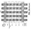
- One popular flash EEPROM architectureutilizes a NAND array, wherein a large number of strings of memory cells are connected through one or more select transistors between individual bit lines and a reference potential. A portion of such an array is shown in plan view in FIG. 2A .
- BL 0 -BL 4represent diffused bit line connections to global vertical metal bit lines (not shown).
- four floating gate memory cellsare shown in each string, the individual strings typically include 16, 32 or more memory cell charge storage elements, such as floating gates, in a column.
- Control gate (word) lines labeled WL 0 -WL 3 and string selection lines DSL and SSLextend across multiple strings over rows of floating gates, often in polysilicon (labeled P 2 in FIG. 2B , a cross-section along line A-A of FIG.
- the control gate linesare typically formed over the floating gates as a self-aligned stack, and are capacitively coupled with each other through an intermediate dielectric layer 19 , as shown in FIG. 2B .
- the top and bottom of the stringconnect to the bit line and a common source line respectively, commonly through a transistor using the floating gate material (P 1 ) as its active gate electrically driven from the periphery.
- P 1floating gate material
- An individual cell within a columnis read and verified during programming by causing the remaining cells in the string to be turned on hard by placing a relatively high voltage on their respective word lines and by placing a relatively lower voltage on the one selected word line so that the current flowing through each string is primarily dependent only upon the level of charge stored in the addressed cell below the selected word line. That current typically is sensed for a large number of strings in parallel, thereby to read charge level states along a row of floating gates in parallel. Examples of NAND memory cell array architectures and their operation as part of a memory system are found in U.S. Pat. Nos. 5,570,315, 5,774,397 and 6,046,935.
- the charge storage elements of current flash EEPROM arraysare most commonly electrically conductive floating gates, typically formed from doped polysilicon material.
- Another type of memory cell useful in flash EEPROM systemsutilizes a non-conductive dielectric material in place of a conductive floating gate to store charge in a non-volatile manner. Such a cell is described in an article by Chan et al., “A True Single-Transistor Oxide-Nitride-Oxide EEPROM Device,” IEEE Electron Device Letters, Vol. EDL-8, No. 3, March 1987, pp. 93-95.
- a triple layer dielectric formed of silicon oxide, silicon nitride and silicon oxide (“ONO”)is sandwiched between a conductive control gate and a surface of a semi-conductive substrate above the memory cell channel.
- the cellis programmed by injecting electrons from the cell channel into the nitride, where they are trapped and stored in a limited region. This stored charge then changes the threshold voltage of a portion of the channel of the cell in a manner that is detectable.
- the cellis erased by injecting hot holes into the nitride. See also Nozaki et al., “A 1-Mb EEPROM with MONOS Memory Cell for Semiconductor Disk Application,” IEEE Journal of Solid-State Circuits, Vol. 26, No. 4, April 1991, pp. 497-501, which describes a similar cell in a split-gate configuration where a doped polysilicon gate extends over a portion of the memory cell channel to form a separate select transistor.
- Memory cells of a typical non-volatile flash arrayare divided into discrete blocks of cells that are erased together. That is, the block contains the minimum number of cells that are separately erasable together as an erase unit, although more than one block may be erased in a single erasing operation.
- Each blocktypically stores one or more pages of data, a page defined as the minimum number of cells that are simultaneously subjected to a data programming and read operation as the basic unit of programming and reading, although more than one page may be programmed or read in a single operation.
- Each pagetypically stores one or more sectors of data, the size of the sector being defined by the host system. An example is a sector of 512 bytes of user data, following a standard established with magnetic disk drives, plus some number of bytes of overhead information about the user data and/or the block in which it is stored.
- flash EEPROM arraysAs in most all integrated circuit applications, the pressure to shrink the silicon substrate area required to implement some integrated circuit function also exists with flash EEPROM arrays. It is continually desired to increase the amount of digital data that can be stored in a given area of a silicon substrate, in order to increase the storage capacity of a given size memory card and other types of packages, or to both increase capacity and decrease size. Another way to increase the storage density of data is to store more than one bit of data per memory cell charge storage element. This is accomplished by dividing a window of a storage element charge level voltage range into more than two states. The use of four such states allows each cell to store two bits of data, eight states stores three bits of data per cell, and so on. A multiple state flash EEPROM structure and operation is described in U.S. Pat. Nos. 5,043,940 and 5,172,338.
- a significant limitation on the continued shrinking of the size of current non-volatile memory cell arraysis the floating gate dielectric. This cannot practically be made thinner than the approximately 70 Angstrom (7 nm) minimum thickness currently being used without resulting in leakage and difficulties in long term data retention. This means that the voltages required to be coupled to the floating gates to control conduction in the memory cell channels below them cannot be reduced as the size of the various gates and distances between them are reduced. Undesired coupling of voltages between the various gates increases as the distance between them decreases unless a compensating reduction in the voltage levels being used can be made. It is important that such a reduction be made if future scaling of memory arrays is to be made.
- the coupling ratiois equal to the capacitance between the floating and control gates, divided by the capacitance between the floating gate and all adjacent electrodes, most specifically the substrate, as is well known.
- the values of these capacitancesdepend upon the size of the opposing surface areas that are coupled, and the thickness and dielectric constants of the dielectric layers between them. Reduction of the coupling ratio is difficult to achieve in NAND arrays because of their stacked control and floating gate structures.
- the coupling area of the floating gate with the substrateis made smaller as part of a shrink, which as a denominator could result in an increase in the coupling ratio, the coupling area between the floating gate and the control gate is similarly reduced, which causes the numerator to decrease as well.
- Another undesired effect of scalingis an increase in parasitic capacitances between conductive array elements, particularly between adjacent floating gates. Errors in programming or in reading the state of one floating gate can, for example, be caused by the close proximity of the charge stored on the floating gate of an adjacent cell. This coupling can create a significant number of errors in multi-state operation where the allowed range of threshold voltages of the floating gate transistor that is devoted to each state is very small.
- a first plurality of horizontal strips of conductive materialare formed in one direction across the surface of a substrate but separated from it by a tunneling dielectric and separated from each other by gaps in a second direction essentially perpendicular to the first direction, forming a first set of conductive strips.
- the gaps between these stripsare subsequently filled with conductive material insulated from both of the adjacent first conductive strips and the underlying substrate, thus forming a plurality of second conductive strips parallel to the first set of strips.
- a plurality of a third set of parallel strips running in the second directionare then formed and the conductive material of both the first and second set of strips along with the separating insulator are removed in the gaps between the third set of strips. Additionally the substrate is partially etched in this region forming a shallow trench and this trench is filled with an insulator, thereby forming a two dimensional array of conductive elements. Elements from the first set of strips form the floating gates of a non-volatile memory device and a pair of adjacent elements from the second set of strips form the control gates which can be electrically coupled to the adjacent floating gates to control their potential.
- a fourth set of conductive stripsis formed in the first direction with gaps in the second direction such that each individual strip is in ohmic contact with a plurality of control gates formed from a common second strip, thus forming wordlines capable of controlling the potential on each of the underlying control gates.
- An individual floating gatecan store a charge state that can be programmed and read out by varying the potential on the adjacent control gates. This charge state can be a multi-level state representing one or more binary bits of information.
- the region of the substrate under the control gatescan be doped to provide conductivity between adjacent memory cells even the absence of the control gate voltage.
- adjacent floating gates in the first directionmay be offset with respect to each other.
- the first set of stripsmay be formed using spacer technology and their widths and spacings may be less than that directly attainable from the exposure capability of the equipment available to image such patterns.
- either the first set of strips or the second set of stripsmay be recessed at least partially into the silicon surface.
- FIG. 1is a block diagram of a type of memory system in which the memory cell array and operational improvements of the present invention may be implemented;
- FIG. 2Ais a plan view of a prior art NAND array
- FIG. 2Bis a cross-sectional view of the prior art NAND array of FIG. 2A taken along the line A-A;
- FIG. 3is a plan view of an example memory cell array in a NAND configuration
- FIG. 4is a cross-sectional view of the array of FIG. 3 , taken at section A-A thereof;
- FIG. 5Ais a cross-sectional view of the array of FIG. 3 , taken at section B-B thereof;
- FIG. 5Bis a cross-sectional view of the array of FIG. 3 , taken at section C-C thereof,
- FIG. 6is a cross-sectional view of a modified version of the array of FIGS. 3-5 , taken at section B-B, at a corresponding process stage to FIG. 5A of the first embodiment.
- FIGS. 7-10are cross-section views of sequentially formed structures of a second embodiment of the array of FIGS. 3-5 , taken at section A-A of FIG. 3 ;
- FIG. 11is an enlarged cross-sectional view of a memory cell of either of the embodiments of FIGS. 3-5 or 7 - 10 , to illustrate an advantage thereof;
- FIG. 12is a cross-sectional view of an alternate memory cell construction that may be implemented in either of the embodiments of FIGS. 3-5 or 7 - 10 ;
- FIG. 13illustrates the capacitive coupling between gate elements and the substrate of either of the embodiments of FIGS. 3-5 or 7 - 10 ;
- FIG. 14is an equivalent circuit diagram of a memory cell array according to either of the embodiments of FIGS. 3-5 or 7 - 10 ;
- FIG. 15is a table of example memory cell array operating conditions that reference the circuit diagram of FIG. 14 ;
- FIG. 16is a circuit diagram of one NAND string used for illustration of methods of reading the NAND memory
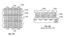
- FIGS. 17A-17N and 17 Pshow sequential processing steps according to an alternate embodiment that form a memory array
- FIGS. 18A-18Dillustrates use of the process of FIGS. 17A-17N and 17 P to form a memory array with a different topography
- FIGS. 19A-19Bshow another embodiment that is a variation of the embodiment of FIGS. 17A-17N and 17 P;
- FIGS. 20A-20Cshow yet another embodiment that is a variation of the embodiments of FIGS. 17A-17N , 17 P and 19 A- 19 B;
- FIG. 21is a flowchart summarizing the processes of FIGS. 17A-20C .
- FIG. 1An example memory system in which the various aspects of the present invention may be implemented is illustrated by the block diagram of FIG. 1 .
- a memory cell array 1 including a plurality of memory cells M arranged in a matrixis controlled by a column control circuit 2 , a row control circuit 3 , a c-source control circuit 4 and a c-p-well control circuit 5 .
- the memory cell array 1is, in this example, of the NAND type that is described above in the Background and in references incorporated therein by reference.
- a control circuit 2is connected to bit lines (BL) of the memory cell array 1 for reading data stored in the memory cells (M), for determining a state of the memory cells (M) during a program operation, and for controlling potential levels of the bit lines (BL) to promote the programming or to inhibit the programming.
- the row control circuit 3is connected to word lines (WL) to select one of the word lines (WL), to apply read voltages, to apply program voltages combined with the bit line potential levels controlled by the column control circuit 2 , and to apply an erase voltage coupled with a voltage of a p-type region on which the memory cells (M) are formed.
- the c-source control circuit 4controls a common source line (labeled as “c-source” in FIG. 1 ) connected to the memory cells (M).
- the c-p-well control circuit 5controls the c-p-well voltage.
- the data stored in the memory cells (M)are read out by the column control circuit 2 and are output to external I/O lines via an I/O line and a data input/output buffer 6 .
- Program data to be stored in the memory cellsare input to the data input/output buffer 6 via the external I/O lines, and transferred to the column control circuit 2 .
- the external I/O linesare connected to a controller 9 .
- the controller 9includes various types of registers and other memory including a volatile random-access-memory (RAM) 10 .
- Command data for controlling the flash memory deviceare inputted to command circuits 7 connected to external control lines that are connected with the controller 9 .
- the command datainforms the flash memory of what operation is requested.
- the input commandis transferred to a state machine 8 that controls the column control circuit 2 , the row control circuit 3 , the c-source control circuit 4 , the c-p-well control circuit 5 and the data input/output buffer 6 .
- the state machine 8can output a status data of the flash memory such as READY/BUSY or PASS/FAIL.
- the controller 9is connected or connectable with a host system such as a personal computer, a digital camera, or a personal digital assistant. It is the host that initiates commands, such as to store or read data to or from the memory array 1 , and provides or receives such data, respectively.
- the controllerconverts such commands into command signals that can be interpreted and executed by the command circuits 7 .
- the controlleralso typically contains buffer memory for the user data being written to or read from the memory array.
- a typical memory systemincludes one integrated circuit chip 11 that includes the controller 9 , and one or more integrated circuit chips 12 that each contain a memory array and associated control, input/output and state machine circuits. The trend, of course, is to integrate the memory array and controller circuits of a system together on one or more integrated circuit chips.
- the memory system of FIG. 1may be embedded as part of the host system, or may be included in a memory card that is removably insertible into a mating socket of a host system.
- a memory cardmay include the entire memory system, or the controller and memory array, with associated peripheral circuits, may be provided in separate cards.
- FIG. 3Major components of a few memory cells of a NAND array are illustrated in plan view in FIG. 3 , with an equivalent circuit thereof shown in FIG. 14 where corresponding elements are indicated by the same reference number as in FIG. 3 but with a prime (′) added.
- Five strings 21 - 25 of series connected memory cellsare included, with three floating gate charge storage elements shown in each string.
- the string 21includes floating gates 27 , 28 and 29
- the string 22has floating gates 30 , 31 and 32
- the string 23includes floating gates 33 , 34 and 35
- the string 24has floating gates 36 , 37 and 38
- the string 25includes floating gates 39 , 40 and 41 . Only a small rectangular array of fifteen memory cells is illustrated for ease of explanation.
- the memory arrayis typically positioned over one or more well regions contained within a common substrate in order to allow the local substrate potential of the memory array to be electrically controlled independent of the common substrate potential.
- substratewith respect to a memory array of transistors throughout this description will include reference to such well regions unless specifically noted.
- Each of the NAND strings 21 - 25includes two select transistors, one at each end of the string, to controllably connect the string between a different one of global bit lines BL 0 -BL 4 ( FIG. 14 ) and a reference potential V S .
- V Sis normally ground during read but may assume a small positive value during programming to assist in minimizing leakage across the source select transistor.
- Voltage V SSLis applied to respective gates 43 - 47 of select transistors T 0S -T 4S control connection of one end of their respective memory cell strings 21 - 25 to V S .
- the other ends of the strings 21 - 25are connected through respective select transistors T 0D -T 4D ( FIG.
- the column control circuits 2( FIG. 1 ) apply a voltage to each bit line that is representative of the specific data to be written, or sense the voltage or current during a read operation.
- the select transistors T 0S -T 4S and T 0D -T 4D( FIG. 14 ) include respective source and drain regions 55 - 64 and 65 - 74 ( FIG. 3 ) in a semiconductor substrate 77 at its surface 79 ( FIGS. 4 , 5 A and 5 B).
- a typical prior art NAND arrayincludes control gate (word) lines extending across multiple strings over rows of floating gates with a suitable insulating dielectric layer therebetween. Close coupling between the control and floating gates is desirable, as discussed above, in order to minimize the control gate voltages that are required to raise the coupled floating gates to the voltage levels necessary for programming and reading their states.
- One control gate (word) lineis used for each row of floating gates.
- the control gatesare typically used as masks to form the floating gates, which then have the same dimensions in the y-direction as the control gates.
- control gate (word) lines 81 - 84are positioned between the floating gates instead of on top of them.
- Each of the control gate linesextends across multiple strings of memory cells and is capacitively coupled through a suitable insulating dielectric, such as multi-layer oxide-nitride-oxide (ONO), to the floating gates on both sides. Additional coupling area is obtained by using the sidewall areas of both sides of the floating gates.
- the floating gatescan be made thicker (higher) than usual in order to increase this coupling area, and the control gates in between them are then made to be at least as thick as the floating gates in order to take advantage of the added coupling area.
- This coupling areamay be controlled largely independently of the coupling area of the floating gates and the substrate, resulting in a desirably high coupling ratio even as the coupling area of the floating gates with the substrate is reduced during future shrinks.
- control gate lines 81 and 82are elongated in the x-direction across the array and separated in the y -direction by the length of the intervening floating gates and the thicknesses of the dielectric layers between them.
- the channel length of the select transistors 43 - 47 and 49 - 53is typically slightly larger than the minimum feature size to ensure it can effectively block all conduction including leakage when the maximum voltage is applied across it.
- FIG. 3A method of forming the array of FIG. 3 , and additional features of the array, can be explained by reference primarily to the orthogonal cross-section views of FIG. 4 (line A-A in the y-direction of FIG. 3 through one string of memory cells), FIG. 5A (line B-B in the x-direction of FIG. 3 along a row of memory cells extending across multiple strings), and FIG. 5B (line C-C in the x-direction of FIG. 3 along a word line).
- a layer 91 of tunnel silicon oxide (SiO 2 )is grown on the surface 79 of the substrate 77 to a thickness of about 8 nm.
- a first layer of doped polysiliconis then formed over at least the area of the array, typically by low -pressure chemical vapor deposition (LPCVD), to a thickness of from 50 to 200 nm. from which the floating gates are later formed. This is thicker than the usual first polysilicon layer in prior art NAND devices, with the result that the later formed floating gates are thicker than previously.
- a thin pad 93 of silicon dioxideis then formed over the top of the polysilicon layer, followed by depositing a layer 95 of silicon nitride (Si 3 N 4 ) of thickness typically between 100 and 300 nm.
- a maskis then formed on the top of the nitride layer for etching the exposed Nitride, oxide pad, polysilicon and tunnel oxide to leave stacked strips elongated across the substrate in the y -direction and separated in the x-direction by the smallest spacing dimension resolvable by the mask formation process.
- the width of these stripsis also preferably made equal to their spacing.
- the etchis anisotropic and exposes the surface 79 of the substrate 77 between these strips.
- a next series of stepsprovides electrical isolation between resulting columns of floating gates by Shallow Trench Isolation (STI).
- the exposed substrate surfaceis then anisotropically etched to form trenches 97 - 100 ( FIG. 5A ) elongated in the y-direction and positioned between the polysilicon/dielectric stack strips in the x-direction. These trenches are preferably etched to a depth of 100-300 nm.
- the exposed silicon surface regionmay be implanted with a light Boron dose to locally increase the field oxide threshold voltage if needed.
- a thick oxide layeris then deposited over the entire array area to completely fill these trenches and the spaces between the polysilicon/dielectric stacked strips.
- CMPChemical Mechanical Polishing
- a relatively flat surfacethen exists across the tops of the nitride strips 95 and thick oxide (regions 97 - 100 in FIG. 5A ).
- high temperature annealingmay be employed to relieve the mechanical stress in the silicon isolation trenches as well as to densify the thick oxide in these trenches. It is also possible to form the array without employing shallow trench isolation, for example by forming thick dielectric isolation above the silicon surface rather than in trenches etched into it.
- a maskis formed with strips extending in the x-direction, perpendicular to the polysilicon/dielectric strips just formed, between which the polysilicon/dielectric strips are removed down to the tunnel dielectric layer 91 by an anisotropic etch.
- the sum of the width of the strips of the mask and the spaces between themare made to be as small as possible, the pitch of the process.
- the actual maskmay be photoresist over another deposited layer of nitride or oxide that is masked and etched to form the masking strips in the x-direction, followed by etching the thus exposed underlying first polysilicon layer and a portion of the exposed field oxide regions. This separates the remaining strips of the first polysilicon layer into the individual floating gates.
- the etch processfirst removes approximately 100-200 nm of exposed field oxide and then the chemistry is changed to selectively remove the entire exposed first polysilicon layer while stopping on the underlying tunnel oxide.
- the first polysilicon layercan also be used to form the select transistor gates 45 and 51 as shown.
- trenchesare formed alongside the first polysilicon strips with lengths in the x-direction. Over the active regions these trenches will extend the full height of the floating gate plus the thickness of masking layers 93 and 95 , and over the field regions they will extend 100-200 nm as was formed during the first polysilicon separation step described previously. It is in these trenches that the control gate lines 81 - 84 , select gates lines 80 and 85 , and source and bit line contacts are formed. But before forming these control gate lines, ions are implanted in the trenches in regions noted on areas of the plan view of FIG. 3 that are lightly dotted. The cross-sectional view of FIG.
- N+ ionsmay typically be implanted with a dose within a range of 5E13-1E15.
- a dielectric layer 103is then formed over the exposed surfaces of the structure, including conforming to the sidewalls and bottom surfaces of the newly formed trenches.
- the layer 103is preferably ONO but may also be a material having a higher dielectric constant.
- a second layer of doped polysiliconis then deposited over the array area, including completely filling the trenches and contacting the dielectric layer 103 .
- This polysiliconis then removed from the top of the structure by CMP, down to the nitride layer 95 (or alternately to the portion of ONO layer 103 immediately in contact with layer 95 ) that is used as a stop, followed by a controlled etch of the polysilicon a small distance into the trenches.
- This polysiliconis also removed using a masking step from those regions of the periphery and array in which contacts to source & drain regions are desired.
- the control gate lines 81 - 84 , the SSL line 80 , and the DSL line 85are the result. These lines are made to extend at least as high as the floating gates to which they are capacitively coupled through the dielectric layer 103 .
- control gate linesare typically driven from one end and extend over a significant portion of the memory array, their series resistance is of concern. Consequently the doped polysilicon may be replaced or supplemented with a variety of materials to address this concern.
- the tops of the control gate linesmay be silicided and a thicker layer than normal may be used in this application since they are defined by CMP rather than chemical etching.
- another conductive materialsuch as tungsten or molybdenum, may be used instead of the doped second polysilicon.
- the control gatescan be formed as a hybrid of polysilicon capped by low resistivity metallic interconnect.
- FIG. 5Bshows a cross section through section C-C of FIG. 3 at this stage of the process.
- the array of NAND stringsis covered with a dielectric insulation layer (not shown), and one or more layers of standard via/metalization (aluminum or copper interconnects) follows to provide electrical access to all bit lines, source lines, word lines and access transistors.
- metalization layerscan be used as local or global interconnects to reduce the resistivity of long word lines that may become exceedingly narrow and therefore quite highly resistive across large memory arrays.
- FIGS. 3-5There are several methods of interconnecting the select gates and implementing the source and drain contacts.
- One such methodis illustrated in FIGS. 3-5 in which the SSL 80 and DSL 85 lines are formed from P 2 (the same material as the word lines).
- the select gate transistorsuse P 1 as their gate material, which should be directly contacted and not left floating.
- One way to accomplish thisis with a direct contact between the horizontal P 2 line and each P 1 gate.
- a maskis used to selectively remove the ONO layer 103 only on the side of the SSL select gate nearest the common source line contact and on the side of the DSL select gate nearest the bit line contact.
- a second P 2 layeris deposited such that the combined thickness of P 2 after CMP polishing and etch-back as described earlier is as shown in FIG. 4 .
- This second P 2 depositionmakes ohmic contact with both the first P 2 deposition and the P 1 gate material and allows the P 2 SSL and DSL lines to directly contact the P 1 gates of the respective select transistors.
- Contacts to the source select transistor's source region which is common to many NAND stringscan be made using a horizontal metal line (M 0 79 in FIG. 3 ), and contacts to the drain select transistor's drain region are made to a vertical metal line (not shown), one metal line for each column of NAND strings. These connections are typically made at the same time as the interconnections in the periphery region.
- An alternate method (not shown) of making contact to the select gatesis to use a mask to open contact regions on top of each gate and interconnect these regions with a horizontal poly or metal line located directly above the select transistors gates, again typically during formation of the periphery circuits and interconnections.
- FIGS. 3-5has a more planar topography than the usual NAND array.
- a primary advantage of this structureis the increased coupling area between the floating gates and the control gates, which leads to an improved capacitive coupling ratio, which in turn allows lower control gate voltages to be used during operation of the memory cell array. Additionally, positioning of the control gate lines between the floating gates in the strings shields these floating gates from each other, thereby significantly reducing, or even eliminating, the undesirable coupling between adjacent floating gates in the column direction. Also, as best shown in FIG.
- control gate lines 81 - 84can be capacitively coupled through the dielectric layers 91 and 103 with the ion implanted source and drain regions in the substrate 77 , and thus employed to raise (boost) the voltage of the substrate surface 79 in these regions.
- the level of the ion implantationcan be made less than usual if the control gate lines are used to control the level of conduction through the implanted regions under them, which this structure allows.
- advantagemay be taken of future reductions of the process pitch to reduce the sizes of floating gates and other elements, and the spaces between them, even though the thickness of the floating gate oxide layer is not reduced. If the thickness of the floating gate oxide is not reduced then the voltage on the floating gate cannot be reduced. However, if the coupling ratio or coupling area between the floating gate and the control gate can be increased, the control gate voltage can be reduced consistent with the requirements of the process shrink. Use of dual control gates coupled to opposing sidewalls of individual floating gates along with increased thickness of the floating gate provides this increased coupling area.
- FIGS. 6-10are cross-sectional views along a NAND string in the y-direction after sequential processing steps are performed.
- FIGS. 4 and 10of the first and second embodiments at comparable stages of their formation, show that the number of memory cell floating gates included in the same length of the NAND string is much higher in FIG. 10 than in FIG. 4 , almost twice as many.
- the structuresappear in the x-direction to be the same.
- the structure of this second embodimenthas the same features and advantages described above for the first embodiment, plus a significantly smaller memory cell size in the y-direction. This is accomplished by a novel combination of undercutting and use of spacers to form elements smaller than the smallest lithographically resolvable element size of the process being used.
- FIG. 6shows a cross section B-B along the x-direction of the array of FIG. 3 after a first series of processing steps to form the vertical strips of polysilicon P 1 (later to become the floating gates) separated by the STI field oxide according to the second embodiment.
- the initial steps in forming the intermediate structure of FIG. 6are the same as described above for the first embodiment as shown in FIG. 5A at a comparable stage of the process.
- a substrate 111is appropriately doped to contain one or more wells and a layer 115 of tunnel oxide is grown over a surface 113 of the substrate.
- a layer of doped polysiliconis then deposited over the oxide, an oxide pad formed on its top, a nitride layer formed over that and the polysilicon/dielectric layers then etched into strips extending in the y-direction.
- the STI trenchesare then formed between the polysilicon strips and filled with oxide. The excess oxide is removed by CMP down to the nitride layers used as a stop.
- One difference with the first embodimentis that the nitride layer corresponding to 95 of FIG. 5A has been removed from the oxide pad 119 , for example using a wet etch.
- a relatively thick (50-200 nm.) dielectric layer 121such as densified silicon dioxide, is then deposited over the oxide pad 119 as shown in FIG. 7 .
- a photoresist mask 123is then formed over this dielectric layer with strips extending in the x-direction, and having widths and spacing in the y-direction determined by the lithographically minimum resolvable element size.
- the dielectric layers 121 and 119are then etched through this mask. The width of the resulting strips can be made smaller than the width of the mask strips by undercutting or over-etching sideways.
- FIG. 8A next series of steps are illustrated by FIG. 8 .
- a thin (approximately 5 nm. thick) oxide pad 125is reformed on the surface of the polysilicon strips.
- the thickness of the deposited nitrideprimarily determines a length L of the spacer, which in turn (as described later) determines the length of the floating gates, which is significantly less than the minimum width of the process being used to form the structure.
- a width W of the undercut oxide strips and the length L of the spacersare preferably chosen to result in substantially equal spacing of the spacers 127 along the lengths of the polysilicon strips 117 , since (as described later) this determines the spacing of the resulting floating gates in the y-direction.
- the materials for the strips 121 and spacers 127may be exchanged, the strips 121 being a nitride and the spacers 127 being an oxide, as the importance of the materials used is to allow removal by etching of the strips 121 while leaving the spacers 127 intact.
- FIGS. 8 and 9This removal and other steps are illustrated by FIGS. 8 and 9 .
- the gaps between the nitride spacers 127( FIG. 8 ) are first filled with oxide so that etching away the oxide strips 121 does not result in over etching the field isolation oxide that is exposed between the NAND strings.
- CMPthen removes any excess oxide, down to tops of the nitride spacers 127 used as CMP stops.
- This oxide between the spacers 127 and the oxide strips 121are then anisotropically etched together back to the top surface of the polysilicon layer 117 , which may be used as end point detection to terminate this oxide etch.
- this isolation oxidecould be masked with a material that is not etched as the oxide strips 121 are removed, and this masking material then removed after the oxide strips 121 have been removed.
- a next stepis to use the remaining nitride spacers 127 as a mask to separate the polysilicon strips, such as the strip 117 , into islands of isolated floating gates.
- Anisotropically etching the polysiliconleaves floating gates 131 - 138 .
- the source and drain ion implantationthen takes place, using the floating gates and covering nitride spacers as a mask.
- the N+ ion implant dosecan be within a range of from 5E13 to 1E15.
- Implanted regions 141 - 147 between the floating gatesare the result. It should be noted that even though floating gate structures 131 - 138 may be tall and extremely thin, they are nonetheless mechanically stable by virtue of support from adjoining walls of the isolation oxide.
- a next stepis the formation of a dielectric layer 151 that conforms to the outside surface of the memory array, as it exists in the stage illustrated in FIG. 9 .
- the dielectric 151is preferably made of ONO to a thickness of between 100 and 200 nm.
- a second layer of doped polysiliconis deposited by LPCVD over the array to completely fill the gaps between floating gates in contact with the dielectric layer 151 . Excess polysilicon material is then removed by CMP back to the nitride layer material in the ONO layer 151 , or, if ONO is not used, to the tops of the nitride spacers 127 that remain as part of the structure.
- control gate lines 153 - 159are separate control gate lines 153 - 159 .
- theymay be formed and treated using any of the variations as described in the first embodiment.
- the exposed surface of the structureis then covered by a passivation dielectric layer, following by forming metal conductive lines and vias to connect the lines with source and drain regions at the end of the memory cell strings, and the control gate lines along their lengths.
- the structure of the second embodimenthas all the advantages described above for the first embodiment, plus a higher density of floating gates along the NAND strings. This added advantage results from making the length L of the floating gates and space W between them smaller than the minimum definable lithographic feature size.
- the typical NAND stringbegins to suffer more severely from edge trapping of electrons in the oxide at the side edges of the floating gate, as indicated at 161 and 163 .
- edge trapping of electrons in the oxideat the side edges of the floating gate, as indicated at 161 and 163 .
- some tunneled electronsremain trapped in thicker portions of the oxide immediately adjoining the tunnel oxide over the channel region. This trapped charge contributes to the conduction state of the memory cell transistor; the more trapped electrons, the higher the threshold voltage during read.
- this oxide trapped chargemay be ejected back into the substrate.
- FIG. 12illustrates a modification that may be made to either of the embodiments described above, in a cross-sectional view taken along a NAND memory cell string.
- the process flowmay be modified to introduce shallow cavities or trenches in the active silicon between adjacent floating gate transistors in the NAND series string. Two such trenches 165 and 167 are shown in FIG. 12 .
- the trenchesare formed by etching into the substrate to a depth of between 20 nm to 50 nm, and is performed after the floating gates have been formed and the exposed tunnel dielectric between them has been removed.
- the silicon of these shallow trenchesPrior to deposition of the second polysilicon layer from which the control gate lines are formed, the silicon of these shallow trenches is implanted with phosphorus or arsenic, typically to a dose of between 5E13 and 1E15 at a low energy, to form source and drain regions 169 and 171 .
- a p-type doping of the memory cell channel regions of the substratewhich typically takes place at an initial stage of the processing, can be made sufficiently low that the silicon surface in these trenches is inverted when the overlying control gate is held to a slightly positive voltage (VCG>0.5V).
- VCG>0.5Vslightly positive voltage
- the control gate voltagesare set at a sufficiently positive voltage to induce an inversion layer along the surface of the trenches and therefore permit conductivity between adjacent floating gate transistors along the NAND string.
- the N + implant into the silicon source and drain regions along the NAND stringis either at a very low dose, perhaps between 1E13 and 5E13, or is altogether omitted.
- the fundamental element of the new NAND cell structure of both embodiments described aboveis the formation of two, rather than one, control gates, for each floating gate, rather than stacking the control gate over the floating gate as is traditional.
- a schematic representation of thisis given in FIG. 13 to show the coupling between the gates.
- Capacitive coupling C CF1 and C CF2exists between opposing sidewalls of a floating gate FG and respective adjacent control gates CG 1 and CG 2 on opposite sides of the floating gate. This coupling is through the ONO or other interpoly dielectric (not shown) that is positioned between these gates.
- None of the control gatesnecessarily couples to the floating gates from their top surfaces, as is customary in conventional structures. Thus most of the coupling between the two control gates and the floating gates of each transistor is along the vertical walls that they share.
- the capacitive coupling ratio of the floating gate transistor in the new configurationcan be improved greatly from an increased physical height of the floating gate and an opposing control gate.
- the coupling ratiois approximately:
- the tunnel dielectric of capacitor C FSincludes an SiO 2 film of thickness between 7 and 9 nanometers, while the dielectric of capacitors C CF1 and C CF2 is typically a sandwich ONO dielectric with an oxide equivalent electrical thickness of between 14 and 18 nanometers. Therefore, if the area of capacitive coupling along each of the two vertical walls of the floating gate is twice the area of channel coupling, then the coupling ratio equals approximately 0.66, which is quite adequate for proper device operation. If a higher value is desired, so that maximum program and erase voltages can be further decreased, this can be readily achieved by forming all floating gates with a greater thickness. This increases the coupling area with adjacent control gates, without increasing the coupling area of the floating gates with the substrate.
- the new structureprovides a path to scaling down minimum floating gate transistor feature size without reducing the coupling ratio ⁇ , and without the need to maintain very high program and erase voltages in highly scaled NAND devices.
- a set of exemplary voltages that perform these operations in the NAND embodiments described aboveis given in the table of FIG. 15 .
- the row of floating gates 28 , 31 , 34 , 37 and 40( FIGS. 3 and 14 ) is being accessed for programming.
- a single floating gate capacitively coupled with two control gatesresults in an equivalent capacitor divider circuit.
- each of the three capacitances of each of the floating gates with the control gate 82 , the control gate 83 and the substrateare equal.
- V CG1 and V CG2are applied to each of the control gates lines 82 and 83 and 0 volts to the substrate, then the voltage of each of the floating gates in the row will be the sum of these three voltages (40 volts) divided by 3, or 13.3 volts Therefore, there is a voltage drop of 13.3 volts across the tunnel dielectric layer separating the floating gate from the substrate channel region. This creates an extremely high electric field that causes electrons to tunnel from the substrate through the gate dielectric and onto the floating gate (Fowler-Nordheim tunneling). Note that in this discussion we are not including the voltage contribution coming from net negative or positive charge on any floating gate from a previous erase or programming operation.
- Programming voltagesare typically applied in pulse sequences, with typical pulse duration of several microseconds.
- the unselected rows of floating gates on either side of this rowshould not be allowed to be affected.
- Floating gates 27 , 30 , 33 , 36 and 39are in one of these adjacent rows and floating gates 29 , 32 , 35 , 38 and 41 in the other ( FIGS. 3 and 14 ).
- one side of each of these floating gatesis capacitively coupled to one of the control gates 82 and 83 that are at 20 volts, in this example. But the opposite side of each of these floating gates is at the same time capacitively coupled with either of the control gates 81 or 84 .
- the floating gate voltages in these unselected rowswill be about 7.3 volts. This voltage across the floating gate oxide will be insufficient to cause electrons to tunnel through the oxide from the substrate channel during the programming pulses.
- 16shows one NAND string consisting of 8 transistors (T 0 -T 7 ) and 9 word lines (WL 0 -WL 8 ) for simplicity, but it is assumed that the actual array consists of multiple parallel NAND strings, each with 16, 32 or more transistors as described previously in regard to FIGS. 3 and 14 .
- T 4multi-state transistor
- the desired reading mechanismis successive increase of the floating gate voltage until bit line conduction is observed
- the voltage on the floating gateshould be increased sequentially from a low value to the high value (3.3 volt) in nearly as many steps as there are states in the cell. For example, if four states are stored in the cell, at least three voltage steps are required to differentiate between the four states.
- V R0is chosen as the control gate voltage that when applied to both of the adjacent control gates will distinguish the lowest threshold state (erase) from the lowest programmed charge storage state (“1”). Typical values would be between 0 and 1 volt.
- bit line currentis sensed to determine presence or absence of conduction.
- V R0 voltall word lines at V R0 volt are set to a new voltage, V R1 , and all word lines at 10 ⁇ V R0 volt are set to a new voltage 10 ⁇ V R1 and the absence or presence of bit line current is sensed.
- V R1is chosen to distinguish between the lowest programmed state (“1”) and the next highest programmed state (“2”). This process is continued until all possible programmed states are sensed. This approach maintains a constant and minimum necessary voltage on each floating gate and tends to minimize the possibility of a read disturb condition to the charge state of all floating gates.
- An alternate approach to read the selected floating gate stateis to place VR0 volt on both of the word lines (WL 4 and WL 5 ) immediately adjacent to the selected transistor (T 4 ), 10 ⁇ V R0 volt on the next adjacent word lines (WL 3 and WL 6 ) both above and below the selected cell, and 5 volts on all remaining word lines. As the voltage on the selected word lines is raised, the voltage on the two adjacent word lines can be lowered by the same amount.
- This approachhas the advantage that a maximum of four control gates are being switched but has the disadvantage that the transistors adjacent to the selected transistor are continually stressed more than necessary because their floating gate voltage is held at 5 volts rather than 3.3 volts as in the previous approach.
- Erase by blockis performed the same way as prior art NAND blocks. All control gates in a block are either at 0V (erased block) or floating (non-erased block) while the local substrate (p-well and underlying n-well) for the entire array is raised to ⁇ 20V.
- the voltages shown in the table of FIG. 15are provided by way of an example only, and other voltages may work equally well or even better.
- This conceptmay be employed to use global word lines to access and selectively set the voltages on more than one local control gate (word) lines. Furthermore, as the thicknesses of the various dielectric layers adjacent to each floating gate are scaled down in future generations, all voltages should be correspondingly scaled down to avoid excessively high electric fields with their attendant possibility of shorts and destructive dielectric breakdown.
- a set of elongated vertical strips of floating gate materialare first defined forming strips and used as a mask to form the isolating trenches separating these strips, thus forming the active regions that will later become the NAND strings. This is then followed by a masking operation forming horizontal strips that are used to etch these vertical strips of floating gate material, thereby forming a two-dimensional array of individual floating gates. Without an additional masking step, horizontal wordlines intrinsically forming control gates are formed in the resulting spaces between the rows of individual floating gates.
- elongated strips of floating gate materialare formed in the horizontal direction using a first mask and strips of control gate material are formed between these floating gate strips but insulated from them, preferably without the use of an additional mask.
- both the floating gate and control gate stripsare isolated in the vertical direction using a second mask to form a two dimensional array of isolated floating gates and control gates. This second mask defines the active regions that will later become the NAND strings and the isolation regions therebetween.
- an additional layer of conductive materialis deposited and using a third mask, the isolated control gates are interconnected forming word lines running generally in the horizontal direction. Details of several embodiments following this overall approach are described in the following sections. In some of these embodiments spacers are employed to accurately form the elongated floating gate strips to a narrow dimension that is smaller than the minimum lithographic dimension.
- FIG. 17Ais a plan view showing a set of photoresist strips of width W′ and pitch P running horizontally in the X direction.
- FIG. 17Bis a cross section through section A-A of FIG. 17A and shows a collection of layers underlying the photoresist strips 1711 .
- a substrate 1700is appropriately doped to contain one or more wells and a layer of tunnel dielectric 1702 is grown or formed by deposition over a surface 1701 of the substrate, typically to a thickness in the range of 5 nm to 10 nm.
- a layer of polysilicon 1705 having a thickness in the range of 30 to 80 nmis then deposited over dielectric 1702 , an oxide pad 1708 is thermally grown or deposited on its top surface, and a nitride layer 1709 is deposited over the oxide pad forming a composite dielectric layer.
- the polysilicon 1705is typically doped during deposition and will later be patterned to form the individual floating gates.
- the oxide pad 1708may be a low temperature deposited oxide such as TEOS (Tetraethyl Orthosilicate), and its thickness may be in the range of 30 to 60 nm.
- the nitride layer 1709may be in the range of 60 to 100 nm.
- spacers used to etch horizontal strips of floating gate materialis very similar to that described earlier in the Second NAND Array Embodiment, and is repeated here in outline form for the convenience of the reader, although the choice of the specific dielectric materials used to form the spacers has been changed as suggested in that description. It should be clear to a person skilled in the art that the actual materials used for the formation of the spacers need not be dielectric materials. For example, polysilicon material or other deposited layers can be suitably used to define the spacers.
- Dielectric 1702may be a layer of silicon dioxide or a sandwich structure including of one or more thin dielectrics such as silicon nitride, aluminum oxide, hafnium oxide, hafnium silicon oxide, or other wide bandgap or high K dielectrics.
- a photoresist mask 1711is formed over this composite dielectric layer defining a first set of strips 1711 extending in the x-direction through at least major portions of the entire array area, and having width W′ and pitch P in the y-direction determined by the lithographically minimum resolvable element size (refer to plan view FIG. 17A ). At least the top layer of the composite dielectric is then etched through this mask. The width of the resulting strips W can be made smaller than the width of the mask strips W′ by undercutting or over-etching sideways. This may be desirable to arrive at a set of parallel floating gate strips of width W with approximately equal spacings between them while conforming to the photolithographic limitations of the equipment used to define and etch these first set of strips.
- the spacer materialis deposited over the array, typically using an LPCVD process, and is then anisotropically etched to leave spacers 1715 along the walls on both sides of the first set of strips 1709 .
- the spacer materialis silicon oxide and its deposited thickness primarily determines the length L of the spacer, which as described later determines the channel length of the transistor channels to be formed under the floating gates. L can be significantly less than the minimum photolithographic width of the process being used to form the structure W′.
- a width W of the undercut nitride strips and the length L of the spacersare preferably but not necessarily chosen to result in substantially equal spacing of the spacer strips 1715 , since this determines the spacing of the resulting floating gates in the y-direction as described later.
- Lmay be in the range of 15 to 50 nm.
- FIGS. 17C , 17 D, and 17 EThis removal and other steps are illustrated by FIGS. 17C , 17 D, and 17 E.
- Reactive ion etchingmay be used to form the spacers, removing excess spacer material above and in regions between the nitride strips 1709 .
- the nitrideis then removed by chemical etching exposing the oxide layer 1708 everywhere except under the spacers 1715 .
- the oxide 1708 and polysilicon 1705are etched using the spacers as a mask, preferably stopping on the underlying tunnel dielectric layer 1702 , forming a composite stack 1719 .
- spacer 1715is an oxide layer
- its minimum thicknessmust be chosen such as to preserve a sufficient remaining thickness after etching through oxide layer 1708 , so that the remaining spacer can withstand the subsequent etch of polysilicon 1705 .
- the polysilicon etchis preferably chosen to etch the polysilicon at a much faster rate than the spacer material. In other embodiments it may be desirable to remove the tunnel dielectric layer 1702 in the region between the stacks 1719 and re-grow or reform a new dielectric layer. Layers 1708 and 1755 may optionally be removed.
- the next series of steps shown in FIGS. 17F and Gforms parallel sets of control gate material in the slots between the composite strips 1719 containing the floating gate strips.
- An insulating layer 1725 forming the inter-poly dielectric (IPD)is deposited over the composite stack.
- This layeris preferably a composite layer formed of a thermally grown and/or deposited oxide followed by deposited nitride followed by a second layer of deposited oxide (ONO), although other IPD materials including the dielectrics cited earlier with respect to layer 1702 either singularly or in combination are also possible. Portions of this layer or the layer in its entirety may be removed from the top surface of the composite stack, but preferably remains at least on the sidewalls.
- a doping material 1730is implanted into the substrate 1700 in the regions between the floating gate strips.
- This doping materialis of opposite conductivity type from that at the surface of the substrate 1701 and typically several orders of magnitude higher in concentration.
- This stepforms source and drain regions ohmically connecting the channels of the floating gate transistors and providing serial connectivity for the NAND string.
- the concentration of this dopingmay be drastically reduced or the step eliminated so that conductivity between floating gates is influenced or controlled by the control gate as explained earlier in connection with FIG. 13 .
- a layer of polysilicon 1735 Mis deposited, typically doped during deposition, filling the exposed slots and covering the composite strips.
- Other materialsespecially high temperature metals such as Tungsten, Tantalum, Molybdenum singly or in combination with their silicides, may be substituted for polysilicon. Portions of this material will eventually serve as the dual control gates straddling each floating gate in the final device.
- Some of the considerations involved in selecting such a materialinclude overall compatibility with silicon processing and deposition conditions, heat treatments, and anneal environments used later in the process. Additional considerations include the ability to conform and fill very narrow spaces, the use of metals with high workfunction, and the use of low resistivity materials, especially the ability to minimize depletion or voltage drop within the material under high field conditions.
- material 1735 Mis polysilicon it may be capped with a barrier metal such as TiN or TaN, or by selective silicidation, to ensure good ohmic contacting to the ensuing wordline material, as described below.
- control gate strips 1735can be recessed into the silicon substrate as described earlier (see FIG. 12 ).
- the substrate 1700Prior to depositing insulating layer 1725 the substrate 1700 is etched to a depth typically between 20 to 50 nm, and a thin thermal oxide is grown to passivate the substrate and the exposed edges of the floating gate strips. Then layer 1725 is deposited, source-drain formation optionally occurs (in one embodiment by ion implantation), followed by deposition of the control gate material 1735 M.
- This structureincreases the effective channel lengths of the transistors in the NAND string by the extent of the vertical walls of the recesses formed in the substrate.
- the polysilicon or conductive material 1735 M over the floating gate stripsmay be removed using standard etch techniques, reactive ion etching, or CMP, preferably without the use of an additional masking step.
- This type of process often referred to as a damascene processis well known to those skilled in the art, and described in standard reference texts such as “Silicon Processing for the VLSI Era, Volume 4” by Stanley Wolf, published by Lattice Press.
- the resultis that deposited layer 1735 M is formed into a set of parallel control gate strips 1735 , and the array area contains parallel sets of floating gate strips separated by sets of control gate strips, both sets of strips running horizontally.
- control gate lines 17Fare shown as being wider than the floating gate lines, but this for ease of illustration only and in some embodiments the floating gate lines are wider than the control gate lines.
- Control gate strips 1735are shown in FIG. 17I to be essentially rectangular in cross section for ease of drawing, but this is highly idealized in practice where such perfect contours are seldom obtained. In practice they may partially overlap the top of stack 1719 , but the essential feature is that adjacent strips 1735 be isolated from each other at some region over the top surface of stack 1719 .
- the next step in the processis to etch through the parallel floating gate and control gate strips and etch into the silicon substrate thus defining the active areas containing the NAND strings (see FIG. 17H through FIG. 17M ).
- a photoresist layer(possibly formed over additional deposited layers) is applied and masked to form vertical strips 1741 , as shown in FIG. 17H , a plan view of the relevant memory area.
- FIG. 17Ishows a cross section of the structure along section A-A of FIG. 17H with the photoresist 1741 visible over the floating gate stacks 1719 and the control gate strips 1735 .
- the parallel strip structureis etched down to the substrate surface.
- an oxide/nitride etchis performed to cut through layers 1715 and 1708 ( FIG. 17E ) over the floating gate strips if present, and layer 1725 thereby exposing the floating gate material.
- Any insulator over the control gate materialis also removed, and the polysilicon control gate and polysilicon floating gate are etched, stopping at the underlying tunnel dielectric 1702 or the gate insulator under the control gate.
- the floating gate and control gatemay be etched in separate steps. The etch chemistry is changed and these layers are removed in regions not originally covered by photoresist 1741 .
- the silicon substrate 1700is etched, typically to a depth in the range of 100 to 300 nm and the photoresist removed.
- a thin thermal oxide in the range of 2 to 5 nmis typically grown to pacify the exposed silicon edges and an oxide is deposited, filling the trenches and also covering the regions of the floating gates and control gates previously covered by photoresist.
- the deposited oxideis typically densified by heat treatment, such as a one hour anneal in Nitrogen at 850° C.
- This stepis followed by a planarizing step, for example by CMP, reactive ion etching, or other suitable techniques to remove the excess deposited oxide over the active areas leaving a flat surface with a filled oxide region 1745 as shown in FIG. 17L and FIG.
- FIG. 17Mwhich are cross sections through cut lines B-B and C-C of FIG. 17K respectively.
- the sequence of steps involved in etching through the parallel strips and into the substrate followed by filling the resulting trench with a deposited insulator and removing it from over the active regionsis referenced later in this description by the acronym STI (shallow trench isolation).
- STIshallow trench isolation
- the end result of the planarization stepmay result in the deposited oxide not totally filling the trench but being partially removed by overetching or other means.
- control gates 1735are discontinuous and must be interconnected to form wordlines used to apply a common control voltage to all control gates connected to each wordline. This is accomplished as shown in plan view in FIG. 17N , and FIG. 17P , a cross section through cut line A-A of FIG. 17N .
- the exposed top surfaces of the isolated control gatesmust establish a good ohmic contact with the connecting material 1755 that will form the word lines. This is accomplished for example by siliciding these top surfaces or by formation of a barrier metal such as Titanium Nitride or Tungsten Nitride.
- the connecting material 1755 that connects the isolated control gatesis desirably a low resistance material and patterned as wide as possible.
- this materialis a high melting point metal containing excess silicon, forming a silicide such as Tungsten silicide (WSix), Cobalt silicide or Nickel silicide, though many other combinations are possible.
- a silicidesuch as Tungsten silicide (WSix), Cobalt silicide or Nickel silicide, though many other combinations are possible.
- the materialis deposited, annealed to make ohmic contact with the control gate segments 1735 ′, and etched to isolate the parallel lines.
- the patterningmay preferably be accomplished using spacer technology since in this example the wordline pitch is less than the photolithographic limit.
- One example of how this patterning can be accomplishedis to deposit a sheet of Tungsten silicide (WSix) to a thickness of approximately 150 nm followed by a composite capping layer of 20 nm polysilicon followed by 60 nm of silicon nitride.
- the silicon nitrideis then masked and etched leaving horizontal strips of width W at a pitch P, similar to the process described in FIG. 17A earlier.
- a spacer materialis formed on the edge of the silicon nitride strips followed by etching the exposed portions of the polysilicon capping layer.
- the exposed polysilicon silicide layeris removed leaving parallel continuous wordlines under the spacers, the wordlines in ohmic contact with the isolated control gates.
- an interlevel dielectricis deposited to serve as an insulator between the conductive wordlines and subsequent interconnection metal layers.
- Contactsmust be established to each end of the NAND strings, and this may be performed by using a doping mask to limit an ion implantation of doping material (typically Phosphorus or Arsenic) to a defined contact area of the source and bit line regions of the NAND string, followed by removal of the insulation material from at least portions of these regions and subsequent deposition and patterning of a metal or low resistance interconnection material.
- doping materialtypically Phosphorus or Arsenic
- FIG. 18shows an alternate topographical embodiment following the same process outline of FIG. 17 in which alternate columns of floating gates and control gates are slightly displaced in the vertical direction with respect to their neighbors.
- FIG. 18Athat corresponds to FIG. 17D it is seen that the floating gate strips 1805 meander though they are generally elongated in the horizontal direction.
- FIG. 18Bthe space between strips 1805 is filled with strips of control gate material 1825 analogous to material 1725 .
- the photoresist mask design 1841 defining the STI regionscovers the jog regions of the parallel strips and after completion of the STI process steps the result is isolated floating gates 1805 ′ and control gates 1825 ′ in which corresponding gates in adjacent columns are offset with respect to their neighbors. This structure may be advantageous to minimize coupling between floating gates in adjacent columns.
- cross-sectional shape of the floating gate described in these embodimentsis relatively rectangular, included within the scope of the invention is shaping the cross-sectional area to form other types of shapes. Examples of different floating gate shapes are described in U.S. Pat. Nos. 6,894,930 and 5,343,063.
- FIG. 19Ashows a plan view of the completed structure corresponding to FIG. 17N
- FIG. 19Bshows a cross section along section A-A of FIG. 19A .
- the processbegins by growing a thin sacrificial thermal oxide followed by a silicon nitride deposition over a silicon substrate 1900 containing appropriate well regions and having surface 1901 .
- the thickness of the silicon nitrideis related to the desired thickness of the ensuing floating gate, but may be of the order of several hundred nm.
- the silicon nitrideis patterned into horizontal strips using a first mask and the sacrificial oxide exposed in these stripe openings is also removed. Then the exposed silicon substrate is etched to the desired depth, typically in the range of 20 to 100 nm.
- the tunnel dielectric 1902is formed as described above with respect to 1702 .
- the first polysiliconis deposited and etched back using reactive ion etching, CMP, or other means to the original silicon nitride surface.
- CMPreactive ion etching
- the nitride and the remaining sacrificial oxideis removed, resulting in horizontal strips of polysilicon 1905 partially submerged into the substrate surface that will later form the floating gates.
- a second gate oxideis grown over the exposed substrate surface 1901 followed by deposition of insulating layer 1925 as described earlier with respect to layer 1925 .
- source and drain regionsmay be formed equivalent to regions 1730 described earlier.
- a second layer of polysilicon or other conductive material equivalent to layer 1735 Mis deposited and etched back preferably without the use of a photoresist masking step to leave isolated strips of conductive material 1935 spaced between the first set of strips 1905 .
- the pairs of strips 1905 and 1935are isolated using an STI process as described earlier, a field oxide is deposited and etched back to form vertical strips of isolation 1945 and isolated floating gates 1905 ′ and control gates 1935 ′.
- Conductive wordline material 1955 equivalent to 1755 described earlieris deposited and etched to contact the isolated control gates 1935 ′, followed by formation of bit line contacts, interconnection metal layers and their associated contacts and vias.
- the partially submerged floating gate structurecan be formed using spacer technology.
- the processis very similar to that described earlier with respect to FIG. 19 .
- a sacrificial oxide 2004is grown over surface 2001 of silicon substrate 2000 followed by a deposition of silicon nitride.
- the nitrideis patterned and etched into horizontal strips as in Alternate Embodiment 1 using standard photolithography, shown in cross section as 2006 .
- Oxide spacer material 2008is then deposited and etched back to the top surface of the nitride.
- a second layer of nitride 2009is deposited completing the structure shown in FIG. 20A .
- This structureis then etched back using the oxide spacer material and the sacrificial oxide as an etch stop, leaving not only the original regions of nitride 2006 but also nitride regions 2006 a in the area between the oxide spacers 2019 where the first layer of nitride was removed, as shown in FIG. 20B .
- the oxide spacersare then removed along with the underlying sacrificial oxide, and etching continues into the substrate to form the shallow trenches 2018 for the floating gates.
- a tunnel dielectric 2002is grown or deposited in the trenches, a first layer of doped polysilicon deposited and planarized as in earlier embodiments resulting in strips of floating gate material 2005 shown in cross section in FIG. 20C .
- the remaining stepsare similar to alternate embodiment 1.
- Nitride 2006 and the underlying sacrificial oxideare removed, a control gate oxide grown, an ONO or equivalent layer deposited over the entire structure, a second control gate material is deposited and planarized forming a parallel set of strips 2035 , STI isolation is formed isolating the floating gate and control gate strips, the individual control gates interconnected into wordlines, and bit line contacts, interconnection metal layers and their associated contacts and vias are formed.
- FIG. 21is a flowchart summarizing the processes of FIGS. 17-20 .
- the Floating Gate (FG) materialis deposited over a substrate containing the tunnel oxide and suitable well regions.
- the floating gateis patterned, either using a photoresist mask or spacers defined from such a mask, forming strips generally running in the horizontal direction though periodic local offsets are included as an option.
- the patterningmay etch shallow groves or depressions into the substrate to partially receive the floating gate material, and the floating gate material etched back to a masking surface thus defining isolated strips as described in FIG. 19 or FIG. 20 .
- some form of insulationis applied to the floating gate strips to insulate them from subsequently deposited control gate material.
- source and drain regionsmay be formed between the floating gate strips.
- the substrateis etched to recess the control gate, creating a longer channel between adjacent floating gates.
- control gate (CG) materialis deposited and defined into strips between the floating gate strips, preferably using a damascene type process as described earlier.
- the floating gate and control gate stripsare isolated in the vertical direction using a photo mask, preferably by etching completely through them and into the substrate, and filling the resulting trenches with a deposited insulator as in an STI process.
- an additional conductive materialis deposited and masked into wordline strips running generally in the horizontal direction and making ohmic contact to the individual control gates.
- global contacts to the top and bottom of the individual NAND stringsare formed and interconnected using one or more conductive interconnect material layers.
- One aspect of the device structure described in these embodiments to be notedis that as the resulting devices sizes are scaled to smaller dimensions and especially through the use of spacer technology the conductivity of the control gate becomes critical. As a high voltage is applied to this node through the wordlines the narrow control gate must couple this voltage onto the floating gate to control proper device operation, and a high coupling ratio is desirable. However, if the conductivity of the control gate is not sufficiently low, a depletion region will form in the control gate and the effective electrical “distance” between the wordline voltage and the adjacent floating gate will increase by the width of this depletion region. In the limit a narrow control gate may be completely depleted and the coupling ratio undesirably reduced.
Landscapes
- Engineering & Computer Science (AREA)
- Microelectronics & Electronic Packaging (AREA)
- Non-Volatile Memory (AREA)
- Semiconductor Memories (AREA)
Abstract
Description
Claims (25)
Priority Applications (3)
| Application Number | Priority Date | Filing Date | Title |
|---|---|---|---|
| US11/279,725US7951669B2 (en) | 2006-04-13 | 2006-04-13 | Methods of making flash memory cell arrays having dual control gates per memory cell charge storage element |
| PCT/US2007/066610WO2007121343A2 (en) | 2006-04-13 | 2007-04-13 | Methods of making flash memory cell arrays having dual control gates per memory cell charge storage element |
| TW096113160ATW200802735A (en) | 2006-04-13 | 2007-04-13 | Methods of making flash memory cell arrays having dual control gates per memory cell charge storage element |
Applications Claiming Priority (1)
| Application Number | Priority Date | Filing Date | Title |
|---|---|---|---|
| US11/279,725US7951669B2 (en) | 2006-04-13 | 2006-04-13 | Methods of making flash memory cell arrays having dual control gates per memory cell charge storage element |
Publications (2)
| Publication Number | Publication Date |
|---|---|
| US20070243680A1 US20070243680A1 (en) | 2007-10-18 |
| US7951669B2true US7951669B2 (en) | 2011-05-31 |
Family
ID=38481130
Family Applications (1)
| Application Number | Title | Priority Date | Filing Date |
|---|---|---|---|
| US11/279,725Active2028-08-06US7951669B2 (en) | 2006-04-13 | 2006-04-13 | Methods of making flash memory cell arrays having dual control gates per memory cell charge storage element |
Country Status (3)
| Country | Link |
|---|---|
| US (1) | US7951669B2 (en) |
| TW (1) | TW200802735A (en) |
| WO (1) | WO2007121343A2 (en) |
Cited By (37)
| Publication number | Priority date | Publication date | Assignee | Title |
|---|---|---|---|---|
| US20080318381A1 (en)* | 2007-06-20 | 2008-12-25 | George Matamis | Methods of forming high density semiconductor devices using recursive spacer technique |
| US20120152460A1 (en)* | 2010-12-15 | 2012-06-21 | Ho-Young Kim | Test mask set and mask set |
| WO2014031341A2 (en) | 2012-08-23 | 2014-02-27 | Sandisk Technologies Inc. | Structures and methods of making nand flash memory |
| WO2014042960A2 (en) | 2012-09-14 | 2014-03-20 | Sandisk Technologies Inc. | Processes for nand flash memory fabrication |
| WO2014042895A1 (en) | 2012-09-14 | 2014-03-20 | Sandisk Technologies Inc. | Methods of making word lines and select lines in nand flash memory |
| US20140115230A1 (en)* | 2012-10-23 | 2014-04-24 | Sandisk Technologies Inc. | Flash Memory with Data Retention Partition |
| WO2014074311A1 (en) | 2012-11-08 | 2014-05-15 | Sandisk Technologies Inc. | Flash memory with data retention bias |
| WO2014172101A1 (en) | 2013-04-18 | 2014-10-23 | Sandisk Technologies Inc. | Memory cell with bilayer floating gate |
| US8886877B1 (en) | 2014-05-15 | 2014-11-11 | Sandisk Technologies Inc. | In-situ block folding for nonvolatile memory |
| US8902652B1 (en) | 2014-05-13 | 2014-12-02 | Sandisk Technologies Inc. | Systems and methods for lower page writes |
| US8932955B1 (en) | 2013-09-04 | 2015-01-13 | Sandisk Technologies Inc. | Triple patterning NAND flash memory with SOC |
| US8942038B2 (en) | 2013-04-02 | 2015-01-27 | SanDisk Technologies, Inc. | High endurance nonvolatile memory |
| US8964467B1 (en) | 2013-12-05 | 2015-02-24 | Sandisk Technologies Inc. | Systems and methods for partial page programming of multi level cells |
| US9009398B2 (en) | 2013-07-02 | 2015-04-14 | Sandisk Technologies Inc. | Write operations for defect management in nonvolatile memory |
| US9043537B1 (en) | 2013-11-21 | 2015-05-26 | Sandisk Technologies Inc. | Update block programming order |
| WO2015084540A1 (en) | 2013-12-02 | 2015-06-11 | Sandisk Technologies Inc. | Multi-die write management |
| US9063671B2 (en) | 2013-07-02 | 2015-06-23 | Sandisk Technologies Inc. | Write operations with full sequence programming for defect management in nonvolatile memory |
| WO2015116453A1 (en) | 2014-01-30 | 2015-08-06 | Sandisk Technologies Inc. | Pattern breaking in multi-die write management |
| US9129854B2 (en) | 2012-10-04 | 2015-09-08 | Sandisk Technologies Inc. | Full metal gate replacement process for NAND flash memory |
| US9182928B2 (en) | 2013-12-06 | 2015-11-10 | Sandisk Technologies Inc. | Lower page only host burst writes |
| US9224744B1 (en) | 2014-09-03 | 2015-12-29 | Sandisk Technologies Inc. | Wide and narrow patterning using common process |
| US9224637B1 (en) | 2014-08-26 | 2015-12-29 | Sandisk Technologies Inc. | Bi-level dry etching scheme for transistor contacts |
| US9245898B2 (en) | 2014-06-30 | 2016-01-26 | Sandisk Technologies Inc. | NAND flash memory integrated circuits and processes with controlled gate height |
| US9330969B2 (en) | 2014-02-12 | 2016-05-03 | Sandisk Technologies Inc. | Air gap formation between bit lines with top protection |
| US9390922B1 (en) | 2015-02-06 | 2016-07-12 | Sandisk Technologies Llc | Process for forming wide and narrow conductive lines |
| US9401275B2 (en) | 2014-09-03 | 2016-07-26 | Sandisk Technologies Llc | Word line with multi-layer cap structure |
| US9425047B1 (en) | 2015-02-19 | 2016-08-23 | Sandisk Technologies Llc | Self-aligned process using variable-fluidity material |
| US9443862B1 (en) | 2015-07-24 | 2016-09-13 | Sandisk Technologies Llc | Select gates with select gate dielectric first |
| US9466523B2 (en) | 2014-07-29 | 2016-10-11 | Sandisk Technologies Llc | Contact hole collimation using etch-resistant walls |
| US9484314B2 (en) | 2014-08-29 | 2016-11-01 | Sandisk Technologies Llc | Word line hook up with protected air gap |
| US9502428B1 (en) | 2015-04-29 | 2016-11-22 | Sandisk Technologies Llc | Sidewall assisted process for wide and narrow line formation |
| US9595444B2 (en) | 2015-05-14 | 2017-03-14 | Sandisk Technologies Llc | Floating gate separation in NAND flash memory |
| US9613971B2 (en) | 2015-07-24 | 2017-04-04 | Sandisk Technologies Llc | Select gates with central open areas |
| US9613806B2 (en) | 2013-09-04 | 2017-04-04 | Sandisk Technologies Llc | Triple patterning NAND flash memory |
| US9627393B2 (en) | 2015-06-30 | 2017-04-18 | Sandisk Technologies Llc | Height reduction in memory periphery |
| US20170133391A1 (en)* | 2014-06-20 | 2017-05-11 | Floadia Corporation | Non-Volatile Semiconductor Memory Device |
| US9858009B2 (en) | 2015-10-26 | 2018-01-02 | Sandisk Technologies Llc | Data folding in 3D nonvolatile memory |
Families Citing this family (38)
| Publication number | Priority date | Publication date | Assignee | Title |
|---|---|---|---|---|
| US6888755B2 (en) | 2002-10-28 | 2005-05-03 | Sandisk Corporation | Flash memory cell arrays having dual control gates per memory cell charge storage element |
| US7951669B2 (en)* | 2006-04-13 | 2011-05-31 | Sandisk Corporation | Methods of making flash memory cell arrays having dual control gates per memory cell charge storage element |
| US7773403B2 (en)* | 2007-01-15 | 2010-08-10 | Sandisk Corporation | Spacer patterns using assist layer for high density semiconductor devices |
| US7795080B2 (en)* | 2007-01-15 | 2010-09-14 | Sandisk Corporation | Methods of forming integrated circuit devices using composite spacer structures |
| US7592225B2 (en)* | 2007-01-15 | 2009-09-22 | Sandisk Corporation | Methods of forming spacer patterns using assist layer for high density semiconductor devices |
| US7704832B2 (en)* | 2007-04-02 | 2010-04-27 | Sandisk Corporation | Integrated non-volatile memory and peripheral circuitry fabrication |
| US7582529B2 (en)* | 2007-04-02 | 2009-09-01 | Sandisk Corporation | Methods of fabricating non-volatile memory with integrated peripheral circuitry and pre-isolation memory cell formation |
| US7807580B2 (en)* | 2007-04-30 | 2010-10-05 | Spansion Llc | Triple poly-si replacement scheme for memory devices |
| US8946803B2 (en)* | 2007-12-06 | 2015-02-03 | Sandisk Technologies Inc. | Method of forming a floating gate with a wide base and a narrow stem |
| KR20090065754A (en)* | 2007-12-18 | 2009-06-23 | 주식회사 동부하이텍 | Semiconductor device and manufacturing method |
| US7807529B2 (en)* | 2007-12-19 | 2010-10-05 | Sandisk Corporation | Lithographically space-defined charge storage regions in non-volatile memory |
| US7615447B2 (en)* | 2007-12-19 | 2009-11-10 | Sandisk Corporation | Composite charge storage structure formation in non-volatile memory using etch stop technologies |
| US8546152B2 (en)* | 2007-12-19 | 2013-10-01 | Sandisk Technologies Inc. | Enhanced endpoint detection in non-volatile memory fabrication processes |
| US7888210B2 (en)* | 2007-12-19 | 2011-02-15 | Sandisk Corporation | Non-volatile memory fabrication and isolation for composite charge storage structures |
| US7736973B2 (en)* | 2008-01-25 | 2010-06-15 | Sandisk Corporation | Non-volatile memory arrays having dual control gate cell structures and a thick control gate dielectric and methods of forming |
| US7907448B2 (en)* | 2008-10-07 | 2011-03-15 | Spansion Llc | Scaled down select gates of NAND flash memory cell strings and method of forming same |
| US7799638B2 (en)* | 2008-10-31 | 2010-09-21 | Macronix International Co., Ltd | Method for forming a memory array |
| US8361856B2 (en) | 2010-11-01 | 2013-01-29 | Micron Technology, Inc. | Memory cells, arrays of memory cells, and methods of forming memory cells |
| US8329567B2 (en) | 2010-11-03 | 2012-12-11 | Micron Technology, Inc. | Methods of forming doped regions in semiconductor substrates |
| US8450175B2 (en) | 2011-02-22 | 2013-05-28 | Micron Technology, Inc. | Methods of forming a vertical transistor and at least a conductive line electrically coupled therewith |
| US8569831B2 (en) | 2011-05-27 | 2013-10-29 | Micron Technology, Inc. | Integrated circuit arrays and semiconductor constructions |
| JP2013098216A (en)* | 2011-10-28 | 2013-05-20 | Elpida Memory Inc | Semiconductor device, memory card, data processing system, and manufacturing method of semiconductor device |
| US8637914B2 (en)* | 2011-12-13 | 2014-01-28 | Micron Technology, Inc. | Memory cells having a plurality of control gates and memory cells having a control gate and a shield |
| US8865595B2 (en)* | 2012-01-05 | 2014-10-21 | Taiwan Semiconductor Manufacturing Company, Ltd. | Device and methods for forming partially self-aligned trenches |
| US9036391B2 (en) | 2012-03-06 | 2015-05-19 | Micron Technology, Inc. | Arrays of vertically-oriented transistors, memory arrays including vertically-oriented transistors, and memory cells |
| US8736061B2 (en)* | 2012-06-07 | 2014-05-27 | GlobalFoundries, Inc. | Integrated circuits having a continuous active area and methods for fabricating same |
| US9006060B2 (en) | 2012-08-21 | 2015-04-14 | Micron Technology, Inc. | N-type field effect transistors, arrays comprising N-type vertically-oriented transistors, methods of forming an N-type field effect transistor, and methods of forming an array comprising vertically-oriented N-type transistors |
| US9129896B2 (en) | 2012-08-21 | 2015-09-08 | Micron Technology, Inc. | Arrays comprising vertically-oriented transistors, integrated circuitry comprising a conductive line buried in silicon-comprising semiconductor material, methods of forming a plurality of conductive lines buried in silicon-comprising semiconductor material, and methods of forming an array comprising vertically-oriented transistors |
| US9478550B2 (en) | 2012-08-27 | 2016-10-25 | Micron Technology, Inc. | Arrays of vertically-oriented transistors, and memory arrays including vertically-oriented transistors |
| US9111853B2 (en) | 2013-03-15 | 2015-08-18 | Micron Technology, Inc. | Methods of forming doped elements of semiconductor device structures |
| TWI512952B (en)* | 2013-05-06 | 2015-12-11 | Macronix Int Co Ltd | Memory device and method of fabricating the same |
| US9362001B2 (en)* | 2014-10-14 | 2016-06-07 | Ememory Technology Inc. | Memory cell capable of operating under low voltage conditions |
| US10192875B2 (en) | 2014-10-14 | 2019-01-29 | Ememory Technology Inc. | Non-volatile memory with protective stress gate |
| US9953717B2 (en)* | 2016-03-31 | 2018-04-24 | Sandisk Technologies Llc | NAND structure with tier select gate transistors |
| TWI588943B (en)* | 2016-10-19 | 2017-06-21 | 力旺電子股份有限公司 | Non-volatile memory |
| US10580492B2 (en)* | 2017-09-15 | 2020-03-03 | Silicon Storage Technology, Inc. | System and method for implementing configurable convoluted neural networks with flash memories |
| CN112768453B (en) | 2018-04-19 | 2024-04-26 | 长江存储科技有限责任公司 | Memory device and method of forming the same |
| TWI685978B (en)* | 2019-01-04 | 2020-02-21 | 力晶積成電子製造股份有限公司 | Semiconductor device and method of manufacturing the same |
Citations (81)
| Publication number | Priority date | Publication date | Assignee | Title |
|---|---|---|---|---|
| JPS60117783A (en) | 1983-11-30 | 1985-06-25 | Toshiba Corp | Non-volatile semiconductor memory device |
| EP0373698A2 (en) | 1988-12-12 | 1990-06-20 | Koninklijke Philips Electronics N.V. | Selective asperity definition technique suitable for use in fabricating floating-gate transistor |
| US5023680A (en) | 1988-11-10 | 1991-06-11 | Texas Instruments Incorporated | Floating-gate memory array with silicided buried bitlines and with single-step-defined floating gates |
| US5025494A (en) | 1988-11-10 | 1991-06-18 | Texas Instruments Incorporated | Cross-point contact-free floating-gate memory array with silicided buried bitlines |
| US5043940A (en) | 1988-06-08 | 1991-08-27 | Eliyahou Harari | Flash EEPROM memory systems having multistate storage cells |
| US5095344A (en) | 1988-06-08 | 1992-03-10 | Eliyahou Harari | Highly compact eprom and flash eeprom devices |
| US5159570A (en) | 1987-12-22 | 1992-10-27 | Texas Instruments Incorporated | Four memory state EEPROM |
| US5172338A (en) | 1989-04-13 | 1992-12-15 | Sundisk Corporation | Multi-state EEprom read and write circuits and techniques |
| US5229632A (en) | 1990-02-19 | 1993-07-20 | Kabushiki Kaisha Toshiba | Electrically erasable memory device having erase-electrode connected to substrate junction |
| JPH0637328A (en) | 1992-07-20 | 1994-02-10 | Fujitsu Ltd | Semiconductor storage device |
| US5343063A (en) | 1990-12-18 | 1994-08-30 | Sundisk Corporation | Dense vertical programmable read only memory cell structure and processes for making them |
| US5422504A (en) | 1994-05-02 | 1995-06-06 | Motorola Inc. | EEPROM memory device having a sidewall spacer floating gate electrode and process |
| US5483487A (en) | 1994-07-05 | 1996-01-09 | Taiwan Semiconductor Manufacturing Comp. Ltd. | Electrically programmable memory device with improved dual floating gates |
| US5570315A (en) | 1993-09-21 | 1996-10-29 | Kabushiki Kaisha Toshiba | Multi-state EEPROM having write-verify control circuit |
| US5677872A (en) | 1995-05-31 | 1997-10-14 | Sandisk Corporation | Low voltage erase of a flash EEPROM system having a common erase electrode for two individual erasable sectors |
| US5736443A (en) | 1996-03-11 | 1998-04-07 | Hyundai Electronics Industries Co., Ltd. | Flash EEPROM cell and method of manufacturing the same |
| JPH10144807A (en) | 1996-11-08 | 1998-05-29 | Sony Corp | Nonvolatile semiconductor memory |
| US5774397A (en) | 1993-06-29 | 1998-06-30 | Kabushiki Kaisha Toshiba | Non-volatile semiconductor memory device and method of programming a non-volatile memory cell to a predetermined state |
| US5877980A (en) | 1996-03-26 | 1999-03-02 | Samsung Electronics Co., Ltd. | Nonvolatile memory device having a program-assist plate |
| US5887145A (en) | 1993-09-01 | 1999-03-23 | Sandisk Corporation | Removable mother/daughter peripheral card |
| US5936887A (en) | 1996-08-13 | 1999-08-10 | Samsung Electronics Co., Ltd. | Non-volatile memory device with NAND type cell structure |
| US5936274A (en) | 1997-07-08 | 1999-08-10 | Micron Technology, Inc. | High density flash memory |
| US5943267A (en) | 1996-05-16 | 1999-08-24 | Altera Corporation | High-density nonvolatile memory cell |
| US5973352A (en) | 1997-08-20 | 1999-10-26 | Micron Technology, Inc. | Ultra high density flash memory having vertically stacked devices |
| US5990514A (en) | 1997-10-04 | 1999-11-23 | Samsung Electronics Co., Ltd. | Nonvolatile semiconductor memory having boosting lines self-aligned with word lines |
| US6013551A (en)* | 1997-09-26 | 2000-01-11 | Taiwan Semiconductor Manufacturing Company, Ltd. | Method of manufacture of self-aligned floating gate, flash memory cell and device manufactured thereby |
| US6044017A (en) | 1997-05-19 | 2000-03-28 | Samsung Electronics, Co., Ltd. | Flash memory device |
| US6046935A (en) | 1996-03-18 | 2000-04-04 | Kabushiki Kaisha Toshiba | Semiconductor device and memory system |
| US6069382A (en) | 1998-02-11 | 2000-05-30 | Cypress Semiconductor Corp. | Non-volatile memory cell having a high coupling ratio |
| JP2000183192A (en) | 1998-12-18 | 2000-06-30 | Sanyo Electric Co Ltd | Nonvolatile semiconductor memory and manufacture thereof |
| US6091104A (en) | 1999-03-24 | 2000-07-18 | Chen; Chiou-Feng | Flash memory cell with self-aligned gates and fabrication process |
| US6103573A (en) | 1999-06-30 | 2000-08-15 | Sandisk Corporation | Processing techniques for making a dual floating gate EEPROM cell array |
| US6127696A (en) | 1991-12-06 | 2000-10-03 | Intel Corporation | High voltage MOS transistor for flash EEPROM applications having a uni-sided lightly doped drain |
| US6133098A (en) | 1999-05-17 | 2000-10-17 | Halo Lsi Design & Device Technology, Inc. | Process for making and programming and operating a dual-bit multi-level ballistic flash memory |
| US6214665B1 (en) | 1997-11-07 | 2001-04-10 | Kabushiki Kaisha Toshiba | Semiconductor memory device having memory cells each having a conductive body of booster plate and a method for manufacturing the same |
| JP2001110917A (en) | 1999-10-04 | 2001-04-20 | Sony Corp | Semiconductor non-volatile memory device and semiconductor device |
| US6222227B1 (en) | 1999-08-09 | 2001-04-24 | Actrans System Inc. | Memory cell with self-aligned floating gate and separate select gate, and fabrication process |
| US20020014645A1 (en) | 2000-06-12 | 2002-02-07 | Toshio Kobayashi | Semiconductor memory device and method for operation thereof |
| US6411548B1 (en) | 1999-07-13 | 2002-06-25 | Kabushiki Kaisha Toshiba | Semiconductor memory having transistors connected in series |
| US20020102774A1 (en) | 1999-02-23 | 2002-08-01 | Dah-Bin Kao | Method and apparatus for split gate source side injection flash memory cell and array with dedicated erase gates |
| US20020127805A1 (en)* | 2001-01-30 | 2002-09-12 | Seiko Epson Corporation | Method of manufacturing semiconductor integrated circuit device including nonvolatile semiconductor memory devices |
| US6472707B1 (en) | 1997-04-08 | 2002-10-29 | Matsushita Electric Industrial Co., Ltd. | Semiconductor memory device |
| EP1265289A2 (en) | 2001-06-06 | 2002-12-11 | Interuniversitair Micro-Elektronica Centrum | Electrically erasable and programmable memory device |
| US6512263B1 (en) | 2000-09-22 | 2003-01-28 | Sandisk Corporation | Non-volatile memory cell array having discontinuous source and drain diffusions contacted by continuous bit line conductors and methods of forming |
| US20030032241A1 (en) | 2001-08-11 | 2003-02-13 | Samsung Electronics Co., Ltd. | Non-volatile memory device having self-aligned gate structure and method of manufacturing same |
| JP2003046005A (en) | 2001-08-01 | 2003-02-14 | Matsushita Electric Ind Co Ltd | Semiconductor storage device and method of manufacturing the same |
| EP1289023A2 (en) | 2001-08-31 | 2003-03-05 | Sharp Kabushiki Kaisha | Nonvolatile semiconductor memory device, fabricating method thereof and operation method thereof |
| US6541815B1 (en) | 2001-10-11 | 2003-04-01 | International Business Machines Corporation | High-density dual-cell flash memory structure |
| US6570214B1 (en)* | 2002-03-01 | 2003-05-27 | Ching-Yuan Wu | Scalable stack-gate flash memory cell and its contactless memory array |
| US6570213B1 (en)* | 2002-02-08 | 2003-05-27 | Silicon Based Technology Corp. | Self-aligned split-gate flash memory cell and its contactless NOR-type memory array |
| US20030109093A1 (en)* | 2001-10-31 | 2003-06-12 | Eliyahou Harari | Multi-state non-volatile integrated circuit memory systems that employ dielectric storage elements |
| US20030155599A1 (en) | 2002-02-21 | 2003-08-21 | International Business Machines Corporation | Twin-cell flash memory structure and method |
| US20030227811A1 (en) | 2002-06-07 | 2003-12-11 | Yoshihisa Sugiura | Non-volatile semiconductor memory |
| US20030232472A1 (en)* | 2002-05-30 | 2003-12-18 | Silicon Based Technology Corp. | Methods of fabbricating a stack-gate non-volatile memory device and its contactless memory arrays |
| US6667510B2 (en)* | 2002-02-19 | 2003-12-23 | Silicon Based Technology Corp. | Self-aligned split-gate flash memory cell and its contactless memory array |
| US20040021171A1 (en) | 2002-08-01 | 2004-02-05 | Nec Electronics Corporation | Non-volatile semiconductor memory device, method for manufacturing same and method for controlling same |
| US6703298B2 (en) | 2002-05-23 | 2004-03-09 | Tower Semiconductor Ltd. | Self-aligned process for fabricating memory cells with two isolated floating gates |
| US20040079988A1 (en)* | 2002-10-28 | 2004-04-29 | Sandisk Corporation | Flash memory cell arrays having dual control gates per memory cell charge storage element |
| US6762092B2 (en) | 2001-08-08 | 2004-07-13 | Sandisk Corporation | Scalable self-aligned dual floating gate memory cell array and methods of forming the array |
| US6807105B2 (en) | 2000-12-15 | 2004-10-19 | Halo Lsi, Inc. | Fast program to program verify method |
| US6853028B2 (en) | 2002-09-04 | 2005-02-08 | Samsung Electronics, Co., Ltd. | Non-volatile memory device having dummy pattern |
| US6859394B2 (en) | 2001-03-06 | 2005-02-22 | Kabushiki Kaisha Toshiba | NAND type non-volatile semiconductor memory device |
| US6885586B2 (en)* | 2002-09-19 | 2005-04-26 | Actrans System Inc. | Self-aligned split-gate NAND flash memory and fabrication process |
| US6894339B2 (en) | 2003-01-02 | 2005-05-17 | Actrans System Inc. | Flash memory with trench select gate and fabrication process |
| US6894930B2 (en) | 2002-06-19 | 2005-05-17 | Sandisk Corporation | Deep wordline trench to shield cross coupling between adjacent cells for scaled NAND |
| US20050145923A1 (en)* | 2004-01-06 | 2005-07-07 | Chiou-Feng Chen | NAND flash memory with enhanced program and erase performance, and fabrication process |
| US6936887B2 (en) | 2001-05-18 | 2005-08-30 | Sandisk Corporation | Non-volatile memory cells utilizing substrate trenches |
| US20060007724A1 (en)* | 2004-02-03 | 2006-01-12 | Chien-Hsing Lee | Double-cell memory device |
| US20060018181A1 (en)* | 2004-06-14 | 2006-01-26 | Kabushiki Kaisha Toshiba | Nonvolatile semiconductor memory |
| US6992929B2 (en) | 2004-03-17 | 2006-01-31 | Actrans System Incorporation, Usa | Self-aligned split-gate NAND flash memory and fabrication process |
| US20060040052A1 (en) | 2001-10-10 | 2006-02-23 | Hongbin Fang | Methods for depositing tungsten layers employing atomic layer deposition techniques |
| US20060081910A1 (en)* | 2004-03-16 | 2006-04-20 | Andy Yu | Non-volatile electrically alterable memory cell for storing multiple data and an array thereof |
| US7038291B2 (en) | 2001-02-06 | 2006-05-02 | Kabushiki Kaisha Toshiba | Semiconductor device and method of fabricating the same |
| US7049652B2 (en) | 2003-12-10 | 2006-05-23 | Sandisk Corporation | Pillar cell flash memory technology |
| US20060231885A1 (en)* | 2001-06-14 | 2006-10-19 | Samsung Electronics Co., Ltd. | Semiconductor device and method of fabricating the same |
| US20060291281A1 (en)* | 2005-06-27 | 2006-12-28 | Pin-Yao Wang | Non-volatile memory, manufacturing and operating method thereof |
| US20070195596A1 (en) | 1999-07-14 | 2007-08-23 | Takashi Kobayashi | Semiconductor integrated circuit device, production and operation method thereof |
| US20070243680A1 (en)* | 2006-04-13 | 2007-10-18 | Eliyahou Harari | Methods of Making Flash Memory Cell Arrays Having Dual Control Gates Per Memory Cell Charge Storage Element |
| US20080067554A1 (en)* | 2006-09-14 | 2008-03-20 | Jae-Hun Jeong | NAND flash memory device with 3-dimensionally arranged memory cell transistors |
| US7362615B2 (en)* | 2005-12-27 | 2008-04-22 | Sandisk Corporation | Methods for active boosting to minimize capacitive coupling effect between adjacent gates of flash memory devices |
| US20080157176A1 (en)* | 2006-12-28 | 2008-07-03 | Kim Won-Joo | Nonvolatile memory device and method of fabricating the same |
- 2006
- 2006-04-13USUS11/279,725patent/US7951669B2/enactiveActive
- 2007
- 2007-04-13WOPCT/US2007/066610patent/WO2007121343A2/enactiveApplication Filing
- 2007-04-13TWTW096113160Apatent/TW200802735A/enunknown
Patent Citations (108)
| Publication number | Priority date | Publication date | Assignee | Title |
|---|---|---|---|---|
| JPS60117783A (en) | 1983-11-30 | 1985-06-25 | Toshiba Corp | Non-volatile semiconductor memory device |
| US5159570A (en) | 1987-12-22 | 1992-10-27 | Texas Instruments Incorporated | Four memory state EEPROM |
| US5043940A (en) | 1988-06-08 | 1991-08-27 | Eliyahou Harari | Flash EEPROM memory systems having multistate storage cells |
| US5095344A (en) | 1988-06-08 | 1992-03-10 | Eliyahou Harari | Highly compact eprom and flash eeprom devices |
| US5025494A (en) | 1988-11-10 | 1991-06-18 | Texas Instruments Incorporated | Cross-point contact-free floating-gate memory array with silicided buried bitlines |
| US5023680A (en) | 1988-11-10 | 1991-06-11 | Texas Instruments Incorporated | Floating-gate memory array with silicided buried bitlines and with single-step-defined floating gates |
| EP0373698A2 (en) | 1988-12-12 | 1990-06-20 | Koninklijke Philips Electronics N.V. | Selective asperity definition technique suitable for use in fabricating floating-gate transistor |
| US5172338B1 (en) | 1989-04-13 | 1997-07-08 | Sandisk Corp | Multi-state eeprom read and write circuits and techniques |
| US5172338A (en) | 1989-04-13 | 1992-12-15 | Sundisk Corporation | Multi-state EEprom read and write circuits and techniques |
| US5229632A (en) | 1990-02-19 | 1993-07-20 | Kabushiki Kaisha Toshiba | Electrically erasable memory device having erase-electrode connected to substrate junction |
| US5343063A (en) | 1990-12-18 | 1994-08-30 | Sundisk Corporation | Dense vertical programmable read only memory cell structure and processes for making them |
| US6127696A (en) | 1991-12-06 | 2000-10-03 | Intel Corporation | High voltage MOS transistor for flash EEPROM applications having a uni-sided lightly doped drain |
| JPH0637328A (en) | 1992-07-20 | 1994-02-10 | Fujitsu Ltd | Semiconductor storage device |
| US5774397A (en) | 1993-06-29 | 1998-06-30 | Kabushiki Kaisha Toshiba | Non-volatile semiconductor memory device and method of programming a non-volatile memory cell to a predetermined state |
| US5887145A (en) | 1993-09-01 | 1999-03-23 | Sandisk Corporation | Removable mother/daughter peripheral card |
| US5570315A (en) | 1993-09-21 | 1996-10-29 | Kabushiki Kaisha Toshiba | Multi-state EEPROM having write-verify control circuit |
| US5422504A (en) | 1994-05-02 | 1995-06-06 | Motorola Inc. | EEPROM memory device having a sidewall spacer floating gate electrode and process |
| US5483487A (en) | 1994-07-05 | 1996-01-09 | Taiwan Semiconductor Manufacturing Comp. Ltd. | Electrically programmable memory device with improved dual floating gates |
| US5677872A (en) | 1995-05-31 | 1997-10-14 | Sandisk Corporation | Low voltage erase of a flash EEPROM system having a common erase electrode for two individual erasable sectors |
| US5736443A (en) | 1996-03-11 | 1998-04-07 | Hyundai Electronics Industries Co., Ltd. | Flash EEPROM cell and method of manufacturing the same |
| US6046935A (en) | 1996-03-18 | 2000-04-04 | Kabushiki Kaisha Toshiba | Semiconductor device and memory system |
| US5877980A (en) | 1996-03-26 | 1999-03-02 | Samsung Electronics Co., Ltd. | Nonvolatile memory device having a program-assist plate |
| US6246607B1 (en) | 1996-03-26 | 2001-06-12 | Samsung Electronics, Co. | Methods of programming nonvolatile memory cells by floating drain or source regions associated therewith |
| US6093605A (en) | 1996-03-26 | 2000-07-25 | Samsung Electronics, Co., Ltd. | Method of manufacturing a nonvolatile memory device having a program-assist plate |
| US6091102A (en) | 1996-05-16 | 2000-07-18 | Altera Corporation | High-density nonvolatile memory cell |
| US5943267A (en) | 1996-05-16 | 1999-08-24 | Altera Corporation | High-density nonvolatile memory cell |
| US6108239A (en)* | 1996-05-16 | 2000-08-22 | Altera Corporation | High-density nonvolatile memory cell |
| US5936887A (en) | 1996-08-13 | 1999-08-10 | Samsung Electronics Co., Ltd. | Non-volatile memory device with NAND type cell structure |
| JPH10144807A (en) | 1996-11-08 | 1998-05-29 | Sony Corp | Nonvolatile semiconductor memory |
| US6472707B1 (en) | 1997-04-08 | 2002-10-29 | Matsushita Electric Industrial Co., Ltd. | Semiconductor memory device |
| US6044017A (en) | 1997-05-19 | 2000-03-28 | Samsung Electronics, Co., Ltd. | Flash memory device |
| US5936274A (en) | 1997-07-08 | 1999-08-10 | Micron Technology, Inc. | High density flash memory |
| US5973352A (en) | 1997-08-20 | 1999-10-26 | Micron Technology, Inc. | Ultra high density flash memory having vertically stacked devices |
| US6013551A (en)* | 1997-09-26 | 2000-01-11 | Taiwan Semiconductor Manufacturing Company, Ltd. | Method of manufacture of self-aligned floating gate, flash memory cell and device manufactured thereby |
| US5990514A (en) | 1997-10-04 | 1999-11-23 | Samsung Electronics Co., Ltd. | Nonvolatile semiconductor memory having boosting lines self-aligned with word lines |
| US6214665B1 (en) | 1997-11-07 | 2001-04-10 | Kabushiki Kaisha Toshiba | Semiconductor memory device having memory cells each having a conductive body of booster plate and a method for manufacturing the same |
| US6455889B2 (en) | 1997-11-07 | 2002-09-24 | Kabushiki Kaisha Toshiba | Semiconductor memory device having memory cells each having a conductive body of booster plate and a method for manufacturing the same |
| US6069382A (en) | 1998-02-11 | 2000-05-30 | Cypress Semiconductor Corp. | Non-volatile memory cell having a high coupling ratio |
| JP2000183192A (en) | 1998-12-18 | 2000-06-30 | Sanyo Electric Co Ltd | Nonvolatile semiconductor memory and manufacture thereof |
| US20020102774A1 (en) | 1999-02-23 | 2002-08-01 | Dah-Bin Kao | Method and apparatus for split gate source side injection flash memory cell and array with dedicated erase gates |
| US6291297B1 (en) | 1999-03-24 | 2001-09-18 | Actrans System Inc. | Flash memory cell with self-aligned gates and fabrication process |
| US6091104A (en) | 1999-03-24 | 2000-07-18 | Chen; Chiou-Feng | Flash memory cell with self-aligned gates and fabrication process |
| US6133098A (en) | 1999-05-17 | 2000-10-17 | Halo Lsi Design & Device Technology, Inc. | Process for making and programming and operating a dual-bit multi-level ballistic flash memory |
| US6103573A (en) | 1999-06-30 | 2000-08-15 | Sandisk Corporation | Processing techniques for making a dual floating gate EEPROM cell array |
| US6411548B1 (en) | 1999-07-13 | 2002-06-25 | Kabushiki Kaisha Toshiba | Semiconductor memory having transistors connected in series |
| US20070195596A1 (en) | 1999-07-14 | 2007-08-23 | Takashi Kobayashi | Semiconductor integrated circuit device, production and operation method thereof |
| US6222227B1 (en) | 1999-08-09 | 2001-04-24 | Actrans System Inc. | Memory cell with self-aligned floating gate and separate select gate, and fabrication process |
| JP2001110917A (en) | 1999-10-04 | 2001-04-20 | Sony Corp | Semiconductor non-volatile memory device and semiconductor device |
| US20020014645A1 (en) | 2000-06-12 | 2002-02-07 | Toshio Kobayashi | Semiconductor memory device and method for operation thereof |
| US6563728B2 (en) | 2000-06-12 | 2003-05-13 | Sony Corporation | Semiconductor memory device and method for operation thereof |
| US6512263B1 (en) | 2000-09-22 | 2003-01-28 | Sandisk Corporation | Non-volatile memory cell array having discontinuous source and drain diffusions contacted by continuous bit line conductors and methods of forming |
| US6807105B2 (en) | 2000-12-15 | 2004-10-19 | Halo Lsi, Inc. | Fast program to program verify method |
| US20020127805A1 (en)* | 2001-01-30 | 2002-09-12 | Seiko Epson Corporation | Method of manufacturing semiconductor integrated circuit device including nonvolatile semiconductor memory devices |
| US7038291B2 (en) | 2001-02-06 | 2006-05-02 | Kabushiki Kaisha Toshiba | Semiconductor device and method of fabricating the same |
| US6859394B2 (en) | 2001-03-06 | 2005-02-22 | Kabushiki Kaisha Toshiba | NAND type non-volatile semiconductor memory device |
| US6936887B2 (en) | 2001-05-18 | 2005-08-30 | Sandisk Corporation | Non-volatile memory cells utilizing substrate trenches |
| EP1265289A2 (en) | 2001-06-06 | 2002-12-11 | Interuniversitair Micro-Elektronica Centrum | Electrically erasable and programmable memory device |
| US20030006450A1 (en) | 2001-06-07 | 2003-01-09 | Luc Haspeslagh | Two bit non-volatile electrically erasable and programmable memory structure, a process for producing said memory structure and methods for programming, reading and erasing said memory structure |
| US6580120B2 (en) | 2001-06-07 | 2003-06-17 | Interuniversitair Microelektronica Centrum (Imec Vzw) | Two bit non-volatile electrically erasable and programmable memory structure, a process for producing said memory structure and methods for programming, reading and erasing said memory structure |
| US20060231885A1 (en)* | 2001-06-14 | 2006-10-19 | Samsung Electronics Co., Ltd. | Semiconductor device and method of fabricating the same |
| JP2003046005A (en) | 2001-08-01 | 2003-02-14 | Matsushita Electric Ind Co Ltd | Semiconductor storage device and method of manufacturing the same |
| US6762092B2 (en) | 2001-08-08 | 2004-07-13 | Sandisk Corporation | Scalable self-aligned dual floating gate memory cell array and methods of forming the array |
| US20030032241A1 (en) | 2001-08-11 | 2003-02-13 | Samsung Electronics Co., Ltd. | Non-volatile memory device having self-aligned gate structure and method of manufacturing same |
| EP1289023A2 (en) | 2001-08-31 | 2003-03-05 | Sharp Kabushiki Kaisha | Nonvolatile semiconductor memory device, fabricating method thereof and operation method thereof |
| US20030047774A1 (en) | 2001-08-31 | 2003-03-13 | Yasuhiro Sugita | Nonvolatile semiconductor memory device, fabricating method thereof and operation method thereof |
| US20060040052A1 (en) | 2001-10-10 | 2006-02-23 | Hongbin Fang | Methods for depositing tungsten layers employing atomic layer deposition techniques |
| US6541815B1 (en) | 2001-10-11 | 2003-04-01 | International Business Machines Corporation | High-density dual-cell flash memory structure |
| US6925007B2 (en) | 2001-10-31 | 2005-08-02 | Sandisk Corporation | Multi-state non-volatile integrated circuit memory systems that employ dielectric storage elements |
| US7341918B2 (en)* | 2001-10-31 | 2008-03-11 | Sandisk Corporation | Multi-state non-volatile integrated circuit memory systems that employ dielectric storage elements |
| US20030109093A1 (en)* | 2001-10-31 | 2003-06-12 | Eliyahou Harari | Multi-state non-volatile integrated circuit memory systems that employ dielectric storage elements |
| US6570213B1 (en)* | 2002-02-08 | 2003-05-27 | Silicon Based Technology Corp. | Self-aligned split-gate flash memory cell and its contactless NOR-type memory array |
| US6667510B2 (en)* | 2002-02-19 | 2003-12-23 | Silicon Based Technology Corp. | Self-aligned split-gate flash memory cell and its contactless memory array |
| US20030155599A1 (en) | 2002-02-21 | 2003-08-21 | International Business Machines Corporation | Twin-cell flash memory structure and method |
| US6570214B1 (en)* | 2002-03-01 | 2003-05-27 | Ching-Yuan Wu | Scalable stack-gate flash memory cell and its contactless memory array |
| US6703298B2 (en) | 2002-05-23 | 2004-03-09 | Tower Semiconductor Ltd. | Self-aligned process for fabricating memory cells with two isolated floating gates |
| US20030232472A1 (en)* | 2002-05-30 | 2003-12-18 | Silicon Based Technology Corp. | Methods of fabbricating a stack-gate non-volatile memory device and its contactless memory arrays |
| US20030227811A1 (en) | 2002-06-07 | 2003-12-11 | Yoshihisa Sugiura | Non-volatile semiconductor memory |
| US6894930B2 (en) | 2002-06-19 | 2005-05-17 | Sandisk Corporation | Deep wordline trench to shield cross coupling between adjacent cells for scaled NAND |
| US6898121B2 (en) | 2002-06-19 | 2005-05-24 | Sandisk Corporation | Deep wordline trench to shield cross coupling between adjacent cells for scaled NAND |
| US20040021171A1 (en) | 2002-08-01 | 2004-02-05 | Nec Electronics Corporation | Non-volatile semiconductor memory device, method for manufacturing same and method for controlling same |
| US6853028B2 (en) | 2002-09-04 | 2005-02-08 | Samsung Electronics, Co., Ltd. | Non-volatile memory device having dummy pattern |
| US6885586B2 (en)* | 2002-09-19 | 2005-04-26 | Actrans System Inc. | Self-aligned split-gate NAND flash memory and fabrication process |
| US20040165443A1 (en)* | 2002-10-28 | 2004-08-26 | Eliyahou Harari | Flash memory cell arrays having dual control gates per memory cell charge storage element |
| US20060187714A1 (en) | 2002-10-28 | 2006-08-24 | Eliyahou Harari | Flash Memory Cell Arrays Having Dual Control Gates Per Memory Cell Charge Storage Element |
| US20100047982A1 (en) | 2002-10-28 | 2010-02-25 | Eliyahou Harari | Flash Memory Cell Arrays Having Dual Control Gates Per Memory Cell Charge Storage Element |
| US7638834B2 (en) | 2002-10-28 | 2009-12-29 | Sandisk Corporation | Flash memory cell arrays having dual control gates per memory cell charge storage element |
| US7486555B2 (en) | 2002-10-28 | 2009-02-03 | Sandisk Corporation | Flash memory cell arrays having dual control gates per memory cell charge storage element |
| US7502261B2 (en) | 2002-10-28 | 2009-03-10 | Sandisk Corporation | Flash memory cell arrays having dual control gates per memory cell charge storage element |
| US6888755B2 (en) | 2002-10-28 | 2005-05-03 | Sandisk Corporation | Flash memory cell arrays having dual control gates per memory cell charge storage element |
| WO2004040583A1 (en) | 2002-10-28 | 2004-05-13 | Sandisk Corporation | Flash memory cell arrays having dual control gates per memory cell charge storage element |
| US7075823B2 (en) | 2002-10-28 | 2006-07-11 | Sandisk Corporation | Flash memory cell arrays having dual control gates per memory cell charge storage element |
| US20060176736A1 (en) | 2002-10-28 | 2006-08-10 | Eliyahou Harari | Flash Memory Cell Arrays Having Dual Control Gates Per Memory Cell Charge Storage Element |
| US20040079988A1 (en)* | 2002-10-28 | 2004-04-29 | Sandisk Corporation | Flash memory cell arrays having dual control gates per memory cell charge storage element |
| US20060202256A1 (en) | 2002-10-28 | 2006-09-14 | Eliyahou Harari | Flash Memory Cell Arrays Having Dual Control Gates Per Memory Cell Charge Storage Element |
| US7303956B2 (en) | 2002-10-28 | 2007-12-04 | Sandisk Corporation | Flash memory cell arrays having dual control gates per memory cell charge storage element |
| US6894339B2 (en) | 2003-01-02 | 2005-05-17 | Actrans System Inc. | Flash memory with trench select gate and fabrication process |
| US7049652B2 (en) | 2003-12-10 | 2006-05-23 | Sandisk Corporation | Pillar cell flash memory technology |
| US20050145923A1 (en)* | 2004-01-06 | 2005-07-07 | Chiou-Feng Chen | NAND flash memory with enhanced program and erase performance, and fabrication process |
| US20060007724A1 (en)* | 2004-02-03 | 2006-01-12 | Chien-Hsing Lee | Double-cell memory device |
| US20060081910A1 (en)* | 2004-03-16 | 2006-04-20 | Andy Yu | Non-volatile electrically alterable memory cell for storing multiple data and an array thereof |
| US6992929B2 (en) | 2004-03-17 | 2006-01-31 | Actrans System Incorporation, Usa | Self-aligned split-gate NAND flash memory and fabrication process |
| US20060018181A1 (en)* | 2004-06-14 | 2006-01-26 | Kabushiki Kaisha Toshiba | Nonvolatile semiconductor memory |
| US20060291281A1 (en)* | 2005-06-27 | 2006-12-28 | Pin-Yao Wang | Non-volatile memory, manufacturing and operating method thereof |
| US7362615B2 (en)* | 2005-12-27 | 2008-04-22 | Sandisk Corporation | Methods for active boosting to minimize capacitive coupling effect between adjacent gates of flash memory devices |
| US20070243680A1 (en)* | 2006-04-13 | 2007-10-18 | Eliyahou Harari | Methods of Making Flash Memory Cell Arrays Having Dual Control Gates Per Memory Cell Charge Storage Element |
| WO2007121343A2 (en) | 2006-04-13 | 2007-10-25 | Sandisk Corporation | Methods of making flash memory cell arrays having dual control gates per memory cell charge storage element |
| US20080067554A1 (en)* | 2006-09-14 | 2008-03-20 | Jae-Hun Jeong | NAND flash memory device with 3-dimensionally arranged memory cell transistors |
| US20080157176A1 (en)* | 2006-12-28 | 2008-07-03 | Kim Won-Joo | Nonvolatile memory device and method of fabricating the same |
Non-Patent Citations (18)
| Title |
|---|
| "Notification of Transmittal of the International Search Report or the Declaration", corresponding PCT application No. PCT/US03/32383, International Searching Authority, European Patent Office, Mar. 24, 2004, 9 pages. |
| Chan et al., "A True Single-Transistor Oxide-Nitride-Oxide EEPROM Device", IEEE Electron Device Letters, vol. EDL-8, No. 3, Mar. 1987, pp. 93-95. |
| Choi et al, "A Triple Polysilicon Stacked Flash Memory Cell With Wordline Self-Boosting Programming", IEEE, 1997, pp. 283-286. |
| Choi et al., "A Novel Booster Plate Technology in High Density NAND Flash Memories for Voltage Scaling-Down and Zero Program Disturbance", IEEE Symposium on VLSI Technology Digest of Technical Papers, 1996, pp. 238-239. |
| EPO, "Office Action," corresponding European Patent Application No. 03770742.9, dated Jun. 11, 2007, 6 pages. |
| Hayashi et al., "Twin MONOS Cell with Dual Control Gates," 2000 Symposium on VLSI Technology Digest of Technical Papers, pp. 122-123. |
| Hsu, Cheng-Yuan et al., "Split-Gate NAND Flash Memory at 120nm Technology Node Featuring Fast Programming and Erase," IEEE 2004 Symposium on VLSI Technology Digest of Technical Papers, Jul. 2004, pp. 78-79. |
| Kim et al., "Fast Parallel Programming of Multi-Level NAND Flash Memory Cells Using the Booster-Line Technology", Symposium on VLSI Technology Digest of Technical Papers, 1997, pp. 65-66. |
| Notification of Transmittal of the International Search Report and the Written Opinion of the International Searching Authority, or the Declaration for SanDisk Corporation, International Application No. PCT/US2007/066610 dated Oct. 23, 2007, 14 pages. |
| Nozaki et al., "A 1-Mb EEPROM With MONOS Memory Cell for Semiconductor Disk Application", IEEE Journal of Solid-State Circuits, vol. 26, No. 4, Apr. 1991, pp. 497-501. |
| Office Action for U.S. Appl. No. 12/607,444 mailed Aug. 12, 2010, 19 pages. |
| Satoh et al., "A Novel Channel Boost Capacitance (CBC) Cell Technology with Low Program Disturbance Suitable for Fast Programming 4Gbit NAND Flash Memories", IEEE Symposium on VLSI Technology Digest of Technical Papers, 1998, pp. 108-109. |
| Suh et al., "A 3.3V 32Mb NAND Flash Memory With Incremental Step Pulse Programming Scheme," IEEE International Solid-State Circuits Conference, Digest of Technical Papers, Feb. 1995, pp. 94-95, 305-306, 128-129 and 350. |
| USPTO, Notice of Allowance for U.S. Appl. No. 11/379,012 mailed Aug. 10, 2007, 14 pages. |
| USPTO, Office Action for U.S. Appl. No. 11/379,004 mailed May 14, 2007, 11 pages. |
| USPTO, Office Action for U.S. Appl. No. 11/379,019 mailed May 14, 2007, 12 pages. |
| Wolf, PhD., Stanley, "Silicon Processing for the VLSI Era, Volume 4-Deep-Submicron Process Technology," published by Lattice Press, 2002, pp. 1-806. |
| Wolf, Silicon Processing for the VLSI Era, vol. 1-Process Technology, Second Edition, copyright 2000, pp. 666-667; pp. 742.* |
Cited By (54)
| Publication number | Priority date | Publication date | Assignee | Title |
|---|---|---|---|---|
| US8143156B2 (en) | 2007-06-20 | 2012-03-27 | Sandisk Technologies Inc. | Methods of forming high density semiconductor devices using recursive spacer technique |
| US20080318381A1 (en)* | 2007-06-20 | 2008-12-25 | George Matamis | Methods of forming high density semiconductor devices using recursive spacer technique |
| US20120152460A1 (en)* | 2010-12-15 | 2012-06-21 | Ho-Young Kim | Test mask set and mask set |
| US9224475B2 (en) | 2012-08-23 | 2015-12-29 | Sandisk Technologies Inc. | Structures and methods for making NAND flash memory |
| WO2014031341A2 (en) | 2012-08-23 | 2014-02-27 | Sandisk Technologies Inc. | Structures and methods of making nand flash memory |
| WO2014042960A2 (en) | 2012-09-14 | 2014-03-20 | Sandisk Technologies Inc. | Processes for nand flash memory fabrication |
| WO2014042895A1 (en) | 2012-09-14 | 2014-03-20 | Sandisk Technologies Inc. | Methods of making word lines and select lines in nand flash memory |
| US9153595B2 (en) | 2012-09-14 | 2015-10-06 | Sandisk Technologies Inc. | Methods of making word lines and select lines in NAND flash memory |
| US9129854B2 (en) | 2012-10-04 | 2015-09-08 | Sandisk Technologies Inc. | Full metal gate replacement process for NAND flash memory |
| WO2014066103A1 (en) | 2012-10-23 | 2014-05-01 | Sandisk Technologies Inc. | Flash memory with data retention partition |
| US20140115230A1 (en)* | 2012-10-23 | 2014-04-24 | Sandisk Technologies Inc. | Flash Memory with Data Retention Partition |
| US9218881B2 (en)* | 2012-10-23 | 2015-12-22 | Sandisk Technologies Inc. | Flash memory blocks with extended data retention |
| WO2014074311A1 (en) | 2012-11-08 | 2014-05-15 | Sandisk Technologies Inc. | Flash memory with data retention bias |
| US8902669B2 (en) | 2012-11-08 | 2014-12-02 | SanDisk Technologies, Inc. | Flash memory with data retention bias |
| US8942038B2 (en) | 2013-04-02 | 2015-01-27 | SanDisk Technologies, Inc. | High endurance nonvolatile memory |
| US8932948B2 (en) | 2013-04-18 | 2015-01-13 | SanDisk Technologies, Inc. | Memory cell floating gate replacement |
| WO2014172101A1 (en) | 2013-04-18 | 2014-10-23 | Sandisk Technologies Inc. | Memory cell with bilayer floating gate |
| US9218242B2 (en) | 2013-07-02 | 2015-12-22 | Sandisk Technologies Inc. | Write operations for defect management in nonvolatile memory |
| US9009398B2 (en) | 2013-07-02 | 2015-04-14 | Sandisk Technologies Inc. | Write operations for defect management in nonvolatile memory |
| US9063671B2 (en) | 2013-07-02 | 2015-06-23 | Sandisk Technologies Inc. | Write operations with full sequence programming for defect management in nonvolatile memory |
| US8932955B1 (en) | 2013-09-04 | 2015-01-13 | Sandisk Technologies Inc. | Triple patterning NAND flash memory with SOC |
| US9613806B2 (en) | 2013-09-04 | 2017-04-04 | Sandisk Technologies Llc | Triple patterning NAND flash memory |
| US9043537B1 (en) | 2013-11-21 | 2015-05-26 | Sandisk Technologies Inc. | Update block programming order |
| US9104556B2 (en) | 2013-11-21 | 2015-08-11 | Sandisk Technologies Inc. | Update block programming order |
| WO2015084540A1 (en) | 2013-12-02 | 2015-06-11 | Sandisk Technologies Inc. | Multi-die write management |
| US9218283B2 (en) | 2013-12-02 | 2015-12-22 | Sandisk Technologies Inc. | Multi-die write management |
| US8964467B1 (en) | 2013-12-05 | 2015-02-24 | Sandisk Technologies Inc. | Systems and methods for partial page programming of multi level cells |
| US9182928B2 (en) | 2013-12-06 | 2015-11-10 | Sandisk Technologies Inc. | Lower page only host burst writes |
| US9244631B2 (en) | 2013-12-06 | 2016-01-26 | Sandisk Technologies Inc. | Lower page only host burst writes |
| US9153324B2 (en) | 2014-01-30 | 2015-10-06 | SanDisk Technologies, Inc. | Pattern breaking in multi-die write management |
| WO2015116453A1 (en) | 2014-01-30 | 2015-08-06 | Sandisk Technologies Inc. | Pattern breaking in multi-die write management |
| US9508437B2 (en) | 2014-01-30 | 2016-11-29 | Sandisk Technologies Llc | Pattern breaking in multi-die write management |
| US9330969B2 (en) | 2014-02-12 | 2016-05-03 | Sandisk Technologies Inc. | Air gap formation between bit lines with top protection |
| US9337085B2 (en) | 2014-02-12 | 2016-05-10 | Sandisk Technologies Inc. | Air gap formation between bit lines with side protection |
| US9355713B2 (en) | 2014-05-13 | 2016-05-31 | Sandisk Technologies Inc. | Systems and methods for lower page writes |
| US8902652B1 (en) | 2014-05-13 | 2014-12-02 | Sandisk Technologies Inc. | Systems and methods for lower page writes |
| US8886877B1 (en) | 2014-05-15 | 2014-11-11 | Sandisk Technologies Inc. | In-situ block folding for nonvolatile memory |
| US9201788B1 (en) | 2014-05-15 | 2015-12-01 | Sandisk Technologies Inc. | In-situ block folding for nonvolatile memory |
| US10680001B2 (en)* | 2014-06-20 | 2020-06-09 | Floadia Corporation | Non-volatile semiconductor memory device |
| US20170133391A1 (en)* | 2014-06-20 | 2017-05-11 | Floadia Corporation | Non-Volatile Semiconductor Memory Device |
| US9245898B2 (en) | 2014-06-30 | 2016-01-26 | Sandisk Technologies Inc. | NAND flash memory integrated circuits and processes with controlled gate height |
| US9466523B2 (en) | 2014-07-29 | 2016-10-11 | Sandisk Technologies Llc | Contact hole collimation using etch-resistant walls |
| US9224637B1 (en) | 2014-08-26 | 2015-12-29 | Sandisk Technologies Inc. | Bi-level dry etching scheme for transistor contacts |
| US9484314B2 (en) | 2014-08-29 | 2016-11-01 | Sandisk Technologies Llc | Word line hook up with protected air gap |
| US9401275B2 (en) | 2014-09-03 | 2016-07-26 | Sandisk Technologies Llc | Word line with multi-layer cap structure |
| US9224744B1 (en) | 2014-09-03 | 2015-12-29 | Sandisk Technologies Inc. | Wide and narrow patterning using common process |
| US9390922B1 (en) | 2015-02-06 | 2016-07-12 | Sandisk Technologies Llc | Process for forming wide and narrow conductive lines |
| US9425047B1 (en) | 2015-02-19 | 2016-08-23 | Sandisk Technologies Llc | Self-aligned process using variable-fluidity material |
| US9502428B1 (en) | 2015-04-29 | 2016-11-22 | Sandisk Technologies Llc | Sidewall assisted process for wide and narrow line formation |
| US9595444B2 (en) | 2015-05-14 | 2017-03-14 | Sandisk Technologies Llc | Floating gate separation in NAND flash memory |
| US9627393B2 (en) | 2015-06-30 | 2017-04-18 | Sandisk Technologies Llc | Height reduction in memory periphery |
| US9443862B1 (en) | 2015-07-24 | 2016-09-13 | Sandisk Technologies Llc | Select gates with select gate dielectric first |
| US9613971B2 (en) | 2015-07-24 | 2017-04-04 | Sandisk Technologies Llc | Select gates with central open areas |
| US9858009B2 (en) | 2015-10-26 | 2018-01-02 | Sandisk Technologies Llc | Data folding in 3D nonvolatile memory |
Also Published As
| Publication number | Publication date |
|---|---|
| WO2007121343A3 (en) | 2007-12-21 |
| US20070243680A1 (en) | 2007-10-18 |
| TW200802735A (en) | 2008-01-01 |
| WO2007121343A2 (en) | 2007-10-25 |
Similar Documents
| Publication | Publication Date | Title |
|---|---|---|
| US7951669B2 (en) | Methods of making flash memory cell arrays having dual control gates per memory cell charge storage element | |
| US7075823B2 (en) | Flash memory cell arrays having dual control gates per memory cell charge storage element | |
| US7795080B2 (en) | Methods of forming integrated circuit devices using composite spacer structures | |
| US8946048B2 (en) | Method of fabricating non-volatile memory with flat cell structures and air gap isolation | |
| US7736973B2 (en) | Non-volatile memory arrays having dual control gate cell structures and a thick control gate dielectric and methods of forming | |
| US7704832B2 (en) | Integrated non-volatile memory and peripheral circuitry fabrication | |
| US7773403B2 (en) | Spacer patterns using assist layer for high density semiconductor devices | |
| US20090162951A1 (en) | Enhanced Endpoint Detection In Non-Volatile Memory Fabrication Processes | |
| US9548311B2 (en) | Non-volatile storage element with suspended charge storage region | |
| US20090162977A1 (en) | Non-Volatile Memory Fabrication And Isolation For Composite Charge Storage Structures | |
| US7592225B2 (en) | Methods of forming spacer patterns using assist layer for high density semiconductor devices | |
| US9224746B2 (en) | Inverted-T word line and formation for non-volatile storage | |
| US20080239821A1 (en) | Nand memory with side-tunneling |
Legal Events
| Date | Code | Title | Description |
|---|---|---|---|
| AS | Assignment | Owner name:SANDISK CORPORATION, CALIFORNIA Free format text:ASSIGNMENT OF ASSIGNORS INTEREST;ASSIGNORS:HARARI, ELIYAHOU;SAMACHISA, GEORGE;REEL/FRAME:017809/0062 Effective date:20060412 | |
| STCF | Information on status: patent grant | Free format text:PATENTED CASE | |
| AS | Assignment | Owner name:SANDISK TECHNOLOGIES INC., TEXAS Free format text:ASSIGNMENT OF ASSIGNORS INTEREST;ASSIGNOR:SANDISK CORPORATION;REEL/FRAME:026334/0729 Effective date:20110404 | |
| FPAY | Fee payment | Year of fee payment:4 | |
| AS | Assignment | Owner name:SANDISK TECHNOLOGIES LLC, TEXAS Free format text:CHANGE OF NAME;ASSIGNOR:SANDISK TECHNOLOGIES INC;REEL/FRAME:038809/0472 Effective date:20160516 | |
| MAFP | Maintenance fee payment | Free format text:PAYMENT OF MAINTENANCE FEE, 8TH YEAR, LARGE ENTITY (ORIGINAL EVENT CODE: M1552); ENTITY STATUS OF PATENT OWNER: LARGE ENTITY Year of fee payment:8 | |
| MAFP | Maintenance fee payment | Free format text:PAYMENT OF MAINTENANCE FEE, 12TH YEAR, LARGE ENTITY (ORIGINAL EVENT CODE: M1553); ENTITY STATUS OF PATENT OWNER: LARGE ENTITY Year of fee payment:12 | |
| AS | Assignment | Owner name:SANDISK TECHNOLOGIES, INC., CALIFORNIA Free format text:ASSIGNMENT OF ASSIGNORS INTEREST;ASSIGNOR:SANDISK TECHNOLOGIES LLC;REEL/FRAME:069796/0423 Effective date:20241227 | |
| AS | Assignment | Owner name:SANDISK TECHNOLOGIES, INC., CALIFORNIA Free format text:PARTIAL RELEASE OF SECURITY INTERESTS;ASSIGNOR:JPMORGAN CHASE BANK, N.A., AS AGENT;REEL/FRAME:071382/0001 Effective date:20250424 Owner name:JPMORGAN CHASE BANK, N.A., AS COLLATERAL AGENT, ILLINOIS Free format text:SECURITY AGREEMENT;ASSIGNOR:SANDISK TECHNOLOGIES, INC.;REEL/FRAME:071050/0001 Effective date:20250424 |