US7949214B2 - Substrate guided relay with pupil expanding input coupler - Google Patents
Substrate guided relay with pupil expanding input couplerDownload PDFInfo
- Publication number
- US7949214B2 US7949214B2US12/266,063US26606308AUS7949214B2US 7949214 B2US7949214 B2US 7949214B2US 26606308 AUS26606308 AUS 26606308AUS 7949214 B2US7949214 B2US 7949214B2
- Authority
- US
- United States
- Prior art keywords
- optical substrate
- light
- input coupler
- guided relay
- major face
- Prior art date
- Legal status (The legal status is an assumption and is not a legal conclusion. Google has not performed a legal analysis and makes no representation as to the accuracy of the status listed.)
- Expired - Fee Related, expires
Links
- 239000000758substrateSubstances0.000titleclaimsabstractdescription177
- 210000001747pupilAnatomy0.000titleclaimsabstractdescription18
- 230000003287optical effectEffects0.000claimsabstractdescription110
- 239000004973liquid crystal related substanceSubstances0.000claimsdescription15
- 210000000887faceAnatomy0.000claimsdescription12
- XUIMIQQOPSSXEZ-UHFFFAOYSA-NSiliconChemical compound[Si]XUIMIQQOPSSXEZ-UHFFFAOYSA-N0.000claimsdescription6
- 238000012545processingMethods0.000claimsdescription6
- 229910052710siliconInorganic materials0.000claimsdescription6
- 239000010703siliconSubstances0.000claimsdescription6
- 238000000576coating methodMethods0.000description27
- 239000011248coating agentSubstances0.000description12
- 230000008901benefitEffects0.000description8
- 238000002310reflectometryMethods0.000description7
- 238000004519manufacturing processMethods0.000description6
- 238000012546transferMethods0.000description4
- BQCADISMDOOEFD-UHFFFAOYSA-NSilverChemical compound[Ag]BQCADISMDOOEFD-UHFFFAOYSA-N0.000description3
- 230000009471actionEffects0.000description3
- 230000008859changeEffects0.000description3
- 230000000694effectsEffects0.000description3
- 238000012986modificationMethods0.000description3
- 230000004048modificationEffects0.000description3
- 229910052709silverInorganic materials0.000description3
- 239000004332silverSubstances0.000description3
- 239000000853adhesiveSubstances0.000description2
- 230000001070adhesive effectEffects0.000description2
- 230000005540biological transmissionEffects0.000description2
- 230000001419dependent effectEffects0.000description2
- 239000003292glueSubstances0.000description2
- 239000000463materialSubstances0.000description2
- 238000000034methodMethods0.000description2
- 230000010287polarizationEffects0.000description2
- 230000008569processEffects0.000description2
- 239000004593EpoxySubstances0.000description1
- VYPSYNLAJGMNEJ-UHFFFAOYSA-NSilicium dioxideChemical compoundO=[Si]=OVYPSYNLAJGMNEJ-UHFFFAOYSA-N0.000description1
- 238000010276constructionMethods0.000description1
- 238000013461designMethods0.000description1
- 125000003700epoxy groupChemical group0.000description1
- 238000005530etchingMethods0.000description1
- 239000005350fused silica glassSubstances0.000description1
- 239000011521glassSubstances0.000description1
- 238000000265homogenisationMethods0.000description1
- 238000005286illuminationMethods0.000description1
- 238000005259measurementMethods0.000description1
- 230000007935neutral effectEffects0.000description1
- 229920000647polyepoxidePolymers0.000description1
- 230000009467reductionEffects0.000description1
- 238000006467substitution reactionMethods0.000description1
- 230000000007visual effectEffects0.000description1
Images


Classifications
- G—PHYSICS
- G02—OPTICS
- G02B—OPTICAL ELEMENTS, SYSTEMS OR APPARATUS
- G02B27/00—Optical systems or apparatus not provided for by any of the groups G02B1/00 - G02B26/00, G02B30/00
- G02B27/0081—Optical systems or apparatus not provided for by any of the groups G02B1/00 - G02B26/00, G02B30/00 with means for altering, e.g. enlarging, the entrance or exit pupil
Definitions
- This inventionrelates generally to optical relay systems, and more particularly to a substrate guided relay that includes an input coupler having one or more reflective surfaces configured to expand received light in at least one dimension.
- Substrate guided relaysare devices that transmit light rays from a source to a viewer.
- substrate guided relaysare optical transfer devices having a light transporting substrate, which may manufactured from glass, fused silica, or other transparent media.
- the substratedirects light from an input coupler to an output coupler.
- the lightis guided along its path by the optical transfer properties of the substrate.
- the output couplerthen delivers the light to the viewer.
- the output couplerdirects the light to a viewing region that is either a projection surface or a user's eye.
- one application for a substrate guided relayis that of a near-to-eye display where the substrate guided relay directs light into the pupil of a user.
- Substrate guided relaysgenerally include three basic components: an input coupler that collects and receives light from a source, a substrate that transfers the light, and an output coupler that delivers light away from the substrate. Once the input coupler collects and receives the light from a source, it delivers the light to the substrate. The substrate then delivers the light to the output coupler which directs the light in the direction preferred for observation.
- the substrate guided relaynot only transmits the light, but can transform the light as well. For example, in many prior art substrate guided relay systems, the substrate also performs expansion of the light. This expansion helps to ensure that the resulting output “bundle” of light is larger than the input “bundle” of light. The expansion also helps to ensure that the output light is uniform and easily viewable.
- the substratecan expand an image after it has been converted to an angularly encoded or collimated image in a variety of sizes.
- FIG. 1a top, plan view of a substrate guided relay.
- FIG. 2illustrates a side, elevation view of a substrate guided relay.
- FIG. 3illustrates a top, plan view of one substrate guided relay in accordance with embodiments of the invention.
- FIG. 4illustrates a side, elevation view of one substrate guided relay in accordance with embodiments of the invention.
- FIG. 5illustrates a top, plan view of one substrate guided relay in accordance with embodiments of the invention.
- FIG. 6illustrates a side, elevation view of one substrate guided relay in accordance with embodiments of the invention.
- FIG. 7illustrates a top, plan view of one substrate guided relay in accordance with embodiments of the invention.
- FIG. 8illustrates a side, elevation view of one substrate guided relay in accordance with embodiments of the invention.
- FIG. 9illustrates a top, plan view of one substrate guided relay in accordance with embodiments of the invention.
- FIG. 10illustrates a side, elevation view of one substrate guided relay in accordance with embodiments of the invention.
- FIG. 11illustrates a top, plan view of one substrate guided relay in accordance with embodiments of the invention.
- FIG. 12illustrates a side, elevation view of one substrate guided relay in accordance with embodiments of the invention.
- FIG. 13illustrates one embodiment of a substrate guided relay being used with a MEMS scanned light source in accordance with embodiments of the invention.
- Embodiments of the present inventionemploy an input coupler having one or more reflective surfaces integrated therein.
- the one or more reflective surfacescan be made from partially reflective layers disposed within the input coupler.
- the reflective surfacescan be full reflector layers disposed within the input coupler.
- the reflective surfacescan be manufactured by configuring a saw-tooth geometry on one side of the input coupler and then using the slanted sides of the saw-tooth pattern as reflective layers.
- an end surface of the substrate itselfcan be configured as a reflective surface. This end reflective surface can then be disposed parallel or coplanar with one of the reflective surfaces of the input coupler, thereby extending the function of the surface of the input coupler. The end may also act as the only reflective surface of the input coupler, making the input coupler a special treatment of the end of the slab guide rather than a separate component.
- the one or more reflective surfacesexpand a receiving surface for input light in at least one direction.
- This expanded receiving surfaceworks to direct light having a cross section larger in one dimension than the input coupler into the optical substrate.
- the one or more reflective layerscollect the expanded light received by the input coupler and direct this expanded light into the optical substrate.
- the expanded receiving surfaceis suitable, for instance, for larger collimated input beams such as those generated by liquid crystal display sources, liquid crystal on silicon sources, and digital light processing sources.
- the expanded receiving surfacehelps facilitate uniform illumination in the output image.
- the inventionis not limited to large input sources, however. As will be illustrated below, embodiments of the invention can also be used with small light sources such as Microelectromechanical System (MEMS) light sources.
- MEMSMicroelectromechanical System
- FIGS. 1 and 2illustrated therein is one embodiment of a substrate guided relay 100 having an input coupler 101 , an optical substrate 102 , and an output coupler 103 .
- FIG. 1is a top, plan view of the substrate guided relay 100
- FIG. 2is a side elevation view of the substrate guided relay 100 .
- Embodiments and operating characteristics of such substrate guided relaysare described in commonly assigned, copending U.S. patent application Ser. No. 11/775,511, filed Jul. 10, 2007, entitled “Substrate-Guided Relays for Use with Scanned Beam Light Sources,” which is incorporated herein by reference.
- the input coupler 101is coupled to the optical substrate at an angle 105 .
- This angleaffects how light leaves the input coupler 101 and enters the optical substrate 102 .
- This angle 105is generally between 30 and 60 degrees. The manufacturing tolerances associated with connecting the input coupler 101 to the optical substrate 102 at this angle 105 are relatively precise.
- the input coupler 101collects and receives light, such as light from a light source 110 .
- the input coupler 101can act as a light homogenizing device. In this capacity the input coupler 101 make copies of incoming light before the light exits the input coupler 101 .
- Examples of this type of input couplerare disclosed in commonly assigned, co-pending U.S. patent application Ser. Nos. 12/167,892 and 12/167,882, entitled “Optical Substrate Guided Relay with Input Homogenizer” and “Substrate Guided Relay with Homogenizing Input Relay,” each filed on Jul. 3, 2008, each of which is incorporated herein by reference.
- light sourcescan be used with the substrate guided relay 100 .
- Examples of light sourcesinclude light emitting diode light sources, liquid crystal display light sources, processing light sources, digital light processing light sources, or MEMS light sources.
- Lightis delivered from the input coupler 101 to the optical substrate 102 through a first interface 106 .
- the input coupler 101can be coupled to the optical substrate 102 along the first interface 106 in a variety of ways, including adhesives, glues, and epoxies, or through optical contacting. As is known in the art, where the optical contacting process is used, this bond can be enhanced by chemically treating the surfaces prior to contacting.
- the first interface 106can include a partially reflective coating.
- This reflective coatingcan be a metallic coating, such as silver, that is configured to work as a p-polarization partially reflective coating.
- Silver coatingsare useful as they can be used to vary reflectance along the first interface 106 by varying the thickness of the silver layer. For instance, such a coating can have a high reflectance near the input, and a lower reflectance further from the input.
- s-polarization partially reflective coatingscan be used at the first interface 106 as well.
- the reflective coatingcan also be designed to be neutral with respect to polarization or to work with either s-polarzied or p-polarized light.
- S-polarization partially reflective coatingsgenerally include coatings that have an s-polarization reflectance within a thirty to seventy percent range, and a lower (generally less than ten percent or so) reflectance p-polarization reflectance for angles and wavelengths of interest.
- P-polarization partially reflective coatingsgenerally include coatings that reflect both p-polarized light and s-polarized light, and exhibit reflectance of p-polarized light at a wavelength and angle of interest greater than twenty percent operating in the vicinity of Brewster's angle (for a low index material with an index—approximately 1.5—and a high index material with refractive index of 1.7-2.1, the angle is approximately fifty degrees when going from high index to low index, and 30 degrees when going from low index to high index).
- the optical substrate 102can vary in thickness and length.
- the distal end 108 of the optical substrate 102can be squared, semi-hexagonal, rounded, or may take other shapes. Additionally, the top and bottom edges of the optical substrate 102 can take on a variety of shapes or geometrical configurations.
- Light passing along the optical substrate 102is generally confined within the optical substrate 102 by the principles of total internal inflection. Alternatively, the light passing through the optical substrate 102 but may be confined by within the optical substrate 102 some other means such as reflective coatings. When the light reflects off a edge of the optical substrate 102 , e.g., edge 107 , it is generally absorbed. Partially reflective coatings, including s-polarization partially reflective coatings, can be used along the faces of the optical substrate to assist with total internal reflection transfer. Coatings may also be used to modify, enhance, or otherwise change the phase change that occurs on each reflection.
- the output coupler 103is configured to receive light from the optical substrate 102 and to enable a viewer (not shown) to see a displayed image, whether it be projected on a projection surface or directed into the viewer's eye.
- the output coupler 103directs light to the viewer through a plurality of partially reflective layers 104 . Note that the output coupler 103 may be disposed either on top of, or beneath, the optical substrate 102 .
- the output coupler 103can be coupled to the optical substrate 102 in a variety of ways, including adhesives, glues, or optical contacting.
- the second interface 109which occurs between the optical substrate 102 and the output coupler 103 , can include a partially reflective coating.
- the output coupler 103can further include a series of partially reflective layers 104 that are configured to receive light from the optical substrate 102 and to direct the light away from the substrate guided relay 100 .
- the array of partially reflective layers 104helps both to direct light away from the substrate guided relay 100 and to expand the exit pupil of the overall device. Note that while partially reflective coatings are used as the partially reflective layers 104 in one embodiment, it will be clear to those of ordinary skill in the art having the benefit of this disclosure that the invention is not so limited. Other devices, including diffractive elements, holograms or lenses, may also be used in conjunction with the output coupler 103 .
- FIGS. 3 and 4illustrated therein is one substrate guided relay 300 in accordance with embodiments of the invention.
- FIG. 3is a top, plan view
- FIG. 4is a side, elevation view.
- the substrate guided relay 300includes an input coupler 301 , an optical substrate 302 , and an output coupler 303 .
- the optical substrate 302has at least one major face 411 .
- the optical substratehas two major faces—a first major face 411 and a second major face 412 .
- the input coupler 301 and output coupler 303are both coupled to a single face—the first major face 411 .
- the input coupler 301 and output coupler 303are coupled to the first major face 411 by optical contacting.
- both the input coupler 301 and output coupler 303are coupled to one major face, as will be illustrated in more detail below, they may be coupled to alternate faces, such as with the input coupler 301 being coupled to the second major face 412 while the output coupler 303 is coupled to the first major face 411 , or vice versa. Additionally, they may both be coupled to the opposite major face—i.e., the second major face 412 .
- a partially reflective coatingmay be disposed between the input coupler 301 and the optical substrate 302 .
- the input coupler 301can be coupled to the optical substrate 302 with no partially reflective coating disposed therebetween.
- the output coupler 303is disposed distally across the optical substrate 302 from the input coupler 301 .
- the output coupler 303is configured to receive light from the optical substrate 302 .
- a partially reflective coatingsuch as a fifty percent s-polarizing partially reflective coating, may be disposed between the output coupler 303 and the optical substrate 302 . Note that this coating can be designed so as to have a varying reflectance layer across its interface.
- regions of the output coupler 303 disposed closer to the input coupler 301may have an area of higher reflectivity (such as sixty percent), while regions of the output coupler 303 disposed more distally relative to the input coupler 301 may have an area of lower reflectivity (such as forty percent).
- the varied reflectivity surfacemay have discrete sections, or may continually vary, such as incrementally varying from a high reflectivity at area to a low reflectivity at area.
- reflectivitymay vary as a function of angle of incident light, polarization of incident light, wavelength of incident light, or any combination thereof. Varying the reflectivity/transmissivity provides—in some applications—for a different transmission of light beams from the optical substrate 302 to the output coupler 303 .
- the output coupler 303includes a plurality of partially reflective layers 304 that are configured to direct light away from the substrate guided relay 300 as an output image.
- the plurality of partially reflective layers 304is disposed within the output coupler 303 and comprises a plurality of partially reflective coatings. Partially reflective coatings provide a visual image to a viewer while still permitting the viewer to see through the overall substrate guided relay 300 . As such, a user employing the substrate guided relay 300 as a display apparatus in eyeglasses would be able to concurrently see both images afar and images presented by the substrate guided relay 300 .
- the one or more partially reflective layers 304may be disposed substantially parallel with one another. In some applications, the one or more partially reflective layers 304 may have substantially similar partial reflection coatings creating a substantially uniform output coupler transmission so that ambient light passing through the output coupler 303 is substantially uniform.
- the input coupler 301includes one or more internal layers 414 that are configured to expand the functional receiving surface for received light in at least one direction. With the expanded functional surface, the input coupler 301 can “couple in” different portions of an extended collimated source, such as a spatially extended image produced by liquid crystal display systems, liquid crystal on silicon systems, digital light projection systems, and so forth.
- the input coupler 301does this by reflecting portions of the expanded, received light off the one or more internal layers 414 into the optical substrate 302 .
- the one or more internal layers 414comprise a series of partially reflective layers such as those in the output coupler 303 .
- the one or more internal layers 414comprise reflectors (reflectors can be used because a user generally needn't look through the input coupler 301 ).
- the one or more internal layers 414are configured to direct light from the input coupler 301 into the optical substrate 302 by reflecting portions of the light off each internal layer 414 .
- the one or more internal layers 414may even expand the light in at least one direction. By being able to “catch” a wider beam of light, the one or more internal layers 414 provide an expanded functional surface for the input beam. This can best be seen in FIG. 4 .
- Light ray 421reflects off of one of the internal layers 414 into the optical substrate 302 . This light ray 421 then begins bouncing along the optical substrate 402 , confined by substantially total internal reflection, until it passes to the output coupler 303 .
- light ray 422reflects off of one of the internal layers 414 into the optical substrate 302 and bounces along the optical substrate 402 until it passes to the output coupler 303 .
- the one or more internal layers 414have the effect of expanding the functional surface of the input beam in the X-direction 423 prior to delivering the received light to the optical substrate 302 . Expansion of the pupil of light is handled by the optical substrate 302 .
- the one or more internal layers 414comprise between one and ten layers.
- etching processescan provide five hundred or more internal layers 414 .
- smaller light sourcessuch as MEMS sources—will use fewer layers while larger light sources—such as liquid crystal display light sources—will use more layers.
- MEMS sourcessuch as MEMS sources
- larger light sourcessuch as liquid crystal display light sources—will use more layers.
- MEMS sourceonly one or two reflective layers may be used in the input coupler 301 .
- a liquid crystal display sourceis used, five or six reflective layers may be used in the input coupler 301 .
- the number of reflective layersmay be determined by application requirements for the substrate guided relay 300 . Where larger numbers of reflective layers are used, the input coupler 301 can be manufactured thinner than when fewer layers are used.
- the one or more internal layers 414can be used to expand the input beam spatially.
- a 1 millimeter beam with having a 40 degree field of viewcan be transformed into a 2 millimeter beam having a 20 degree field of view.
- the substrate guided relays of the present inventioncan also be used in conjunction with light homogenization devices, as recited in the '892 and '882 applications cited above.
- Embodiments of the present inventionare less expensive to manufacture than are many prior art substrate guided relays. Embodiments can be less expensive because alignment tolerances between the input coupler 301 and the substrate guided relay 300 can be relaxed when compared to prior art systems. In effect, softer manufacturing tolerances can be used while retaining adequate output image resolution.
- the input coupler 301can be configured identically to the output coupler 303 .
- the input coupler 301is different in that it has fewer layers that are totally reflective, while the output coupler 303 has a larger number of partially reflective internal layers.
- the input couplers of the present inventionmay simply be optically contacted to the major faces of the substrates without the precise alignment and angle measurements required by prior art substrate guided relays.
- FIGS. 5 and 6illustrated therein is another substrate guided relay 500 in accordance with embodiments of the invention.
- FIG. 5is a top, plan view
- FIG. 6is a side, elevation view.
- FIGS. 5 and 6illustrates the diversity of placement of the input coupler 501 relative to the optical substrate 502 and output coupler 503 offered by embodiments of the invention. While the embodiment of FIGS. 3 and 4 had the input coupler ( 301 ) and output coupler ( 303 ) coupled to the same major face ( 411 ), in FIGS. 5 and 6 the input coupler 501 and output coupler 503 are coupled to different faces.
- the optical substrate 502includes two major faces, a first major face 611 and a second major face 612 .
- the output coupler 503is coupled to the first major face 611
- the input coupler 501is coupled to the second major face 612 .
- the input coupler 501could be coupled to the first major face 611 while the output coupler 503 was coupled to the second major face 612 .
- the input coupler 501 and output coupler 503could both be coupled to the second major face 612 .
- the illustrationsshow light entering and exiting the substrate guided relay at angles substantially perpendicular to the optical substrate 502 , light may enter the input coupler 501 and any angle. Additionally, light may exit the output coupler 503 at any angle as well. In some typical applications, the light beams enter and exit the substrate guided relay at angles less than 30 degrees.
- one or more internal layers 614 in the input coupler 501are configured to direct light from the input coupler 501 into the optical substrate 502 .
- the one or more internal layers 614provide an expanded receiving surface with which to direct light into the optical substrate 502 .
- the internal layers 614 in the input coupler 501 and internal layers 504 in the output coupler 503work together to provide spatial expansion—they expand the light in at least one direction.
- the internal layers 504 of the output coupler 503make copies of the light directed away from the output coupler 503 so as to expand the pupil of that light. This can best be seen in FIG. 6 .
- Light ray 621reflects off of one of the internal layers 614 into the optical substrate 502 .
- This light ray 621then begins bouncing along the optical substrate 502 , confined by substantially total internal reflection, until it passes to the output coupler 503 .
- the layers 504 of the output coupler 503then expand the pupil of the light and direct it away from the substrate guided relay 500 .
- light ray 622reflects off of one of the internal layers 614 into the optical substrate 502 and bounces along the optical substrate 502 until it passes to the output coupler 503 .
- the one or more internal layers 614have the effect of expanding the receiving surface for the input beam in the X-direction prior to—or while—delivering the received light to the optical substrate 502 . Expansion in other directions is handled by the layers 504 of the optical substrate 502 .
- the internal layers of the output coupler 503provide expansion of the light as it exits the substrate guided relay 500 .
- the reflectors of the output coupler 503perform pupil expansion in one direction, while the internal layers 614 of the input coupler 501 permit a large or already expanded pupil to be coupled into the substrate guided relay 500 .
- Each reflector in the output coupler 503reproduces all or a substantial portion of that pupil.
- the width of the pupil coming out of the output coupler 503is roughly equal to the width of the input beam pupil plus the width of the output coupler 503 .
- the substrate guided relay 500can be configured in the opposite orientation. Light can enter through the first major face 611 and then reflect off the internal layers 614 of the input coupler 501 , which is coupled to the second major face 612 , into the optical substrate 502 . In such a configuration, the angle of the internal layers 614 would be reversed. Note also that while light is drawn as entering the substrate guided relay 500 from the bottom or back and exiting from the bottom or back, light could alternatively enter or exit the substrate guided relay 500 from the front and then exit, or enter from the one side and exit from the opposite side.
- the spacing between the internal layers 614are configured in one embodiment such that the distance between each layer, relative to the major face of the optical substrate to which the input coupler is connected, will receive all the light without being interfered by another internal layer. It is also possible to design the input coupler 501 and/or the output coupler 503 so that some, most, or all light is intended to impinge on two or more layers. In this case the input coupler 501 would perform additional pupil expansion and/or increase or improve the uniformity of the pupil. Generally, in this configuration, the reflectance of the individual layers 614 would be lower. This configuration, which will change depending upon application requirements, is dependent upon the number of internal layers used in the input coupler and their spacing.
- FIGS. 7 and 8illustrated therein is another substrate guided relay 700 in accordance with embodiments of the invention.
- FIG. 7is a top, plan view
- FIG. 8is a side, elevation view.
- the end portion 830 of the optical substrate 702extends at a non-orthogonal angle 831 from one of the major faces 811 , 812 of the optical substrate 702 .
- this end portion 830can be polished, coated, or otherwise configured as a reflector to extend the function of the input coupler 701 .
- either an input coupler edge 832 or one of the internal layers 714can be aligned with the end portion 830 to extend the single-ended spatial extending function.
- the input coupler edge 832can be configured to be parallel or substantially coplanar with the end portion 830 . Where this input coupler edge 832 is configured as a reflector, the input coupler edge 832 and end portion 830 combine to reflect incoming light—expanded spatially in one direction—into the optical substrate 702 .
- one of the internal reflective layers 714 of the input coupler 701can be arranged substantially parallel—or in a substantially coplanar arrangement—with a plane defined by the end portion 830 . Again, this alignment of internal reflective layers 714 and end portion 830 works to extend the expansion function.
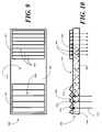
- FIGS. 9 and 10illustrated therein is another substrate guided relay 900 in accordance with embodiments of the invention.
- FIG. 9is a top, plan view
- FIG. 10is a side, elevation view.
- the substrate guided relay 900 of FIGS. 9 and 10works in principle the same way as do previous embodiments.
- the substrate guided relay 900includes, for instance, an optical substrate 902 having at least one major face 1011 and an output coupler 903 coupled to the at least one major face 1011 and having a plurality of partially reflective layers 904 for direct light received from the optical substrate 902 away from the substrate guided relay 900 .
- the substrate guided relay 900also includes an input coupler 901 that is configured to receive light from a source and to expand that received light in one direction and deliver it to the optical substrate 902 .
- the input coupler 901includes reflectors to perform the expansion.
- the reflectorsare configured differently. Rather than being internal reflective layers, in this embodiment the input coupler 901 includes an input coupler face 1041 and a contoured face 1040 .
- the input coupler face 1041is coupled to a major face 1011 of the optical substrate 902 .
- the contoured face 1040is configured as one or more reflectors. In the illustrative embodiment of FIGS.
- the contoured face 1040is configured as a saw-tooth contour so as to expand received light.
- An input coupler 901 of this typehas the advantage of being a “moldable part” in manufacture without a defined internal layer structure.
- the input coupler 901 and the optical substrate 902could be a single molded part with no internal structures.
- the illustrative embodiment shown in FIGS. 9 and 10includes between one and six saw teeth.
- the slanted sides of each of the saw teeth, e.g., saw tooth 1051 and 1052is configured as a reflector to direct light 1021 into the optical substrate.
- the input coupler 901 and output coupler 903can be coupled to a single major face of the optical substrate 902 or different major faces.
- the output coupler 903can be coupled to the first major face 1011 while the input coupler 901 is coupled to the second major face 1012 , or vice-versa.
- lightcan be received through the first major face 1011 or second major face, depending upon the angle of the reflectors of the input coupler 901 .
- FIGS. 11 and 12illustrated therein is another substrate guided relay 1100 in accordance with embodiments of the invention.
- FIG. 11is a top, plan view
- FIG. 12is a side, elevation view.
- the optical substrate 1102includes an end portion 1230 .
- the end portion 1230is adjacent to the input coupler 1101 and extends at a non-orthogonal angle 1231 from one or more of the major faces 1211 , 1212 .
- the configuration of the input coupler 1101can be aligned with the end portion 1230 to expand the functionality of the input coupler 901 .
- a plane defined by at least one of the saw teethcan be aligned in a substantially parallel or coplanar fashion with the end portion 1230 as shown in FIGS. 11 and 12 .
- the input coupler 1101 by itself, or the combination of the input coupler 1101 and the output coupler 1102could be manufactured as molded parts.
- FIG. 13illustrated therein is one substrate guided relay 1300 in accordance with embodiments of the invention being used with a scanned light source 1350 .
- embodiments of the present inventionwork well where input light is spread over an area spanning or substantially spanning the area of the input coupler.
- liquid crystal display sources and liquid crystal on silicon sourceswork well with embodiments of the invention.
- embodiments of the inventionare not so limited. They can equally be used with light sources having small input light beams, such as the MEMS scanned light source 1350 shown in FIG. 13 .
- Examples of MEMS scanning light sources, such as those suitable for use with embodiments of the present invention,are set forth in US Patent Publication No. 2007/0159673, entitled, “Substrate-guided Display with Improved Image Quality,” which is incorporated by reference herein.
- the MEMS scanned light source 1350employs three light sources 1352 , 1353 , 1354 .
- a beam combinercombines the output of light sources 1352 , 1353 , 1354 to produce a combined modulated beam.
- a variable collimation or variable focusing optical element 1355produces a variably shaped beam that is scanned by the scanning mirror 1351 as variably shaped scanned light beam, which is launched into input coupler 1301 of the substrate guided relay 1300 . Note that where a MEMS or other scanned light source is used, the number of reflective layers 1314 used in the input coupler 1301 may be only one or two.
Landscapes
- Physics & Mathematics (AREA)
- General Physics & Mathematics (AREA)
- Optics & Photonics (AREA)
- Projection Apparatus (AREA)
Abstract
Description
Claims (18)
Priority Applications (1)
| Application Number | Priority Date | Filing Date | Title |
|---|---|---|---|
| US12/266,063US7949214B2 (en) | 2008-11-06 | 2008-11-06 | Substrate guided relay with pupil expanding input coupler |
Applications Claiming Priority (1)
| Application Number | Priority Date | Filing Date | Title |
|---|---|---|---|
| US12/266,063US7949214B2 (en) | 2008-11-06 | 2008-11-06 | Substrate guided relay with pupil expanding input coupler |
Publications (2)
| Publication Number | Publication Date |
|---|---|
| US20100111472A1 US20100111472A1 (en) | 2010-05-06 |
| US7949214B2true US7949214B2 (en) | 2011-05-24 |
Family
ID=42131503
Family Applications (1)
| Application Number | Title | Priority Date | Filing Date |
|---|---|---|---|
| US12/266,063Expired - Fee RelatedUS7949214B2 (en) | 2008-11-06 | 2008-11-06 | Substrate guided relay with pupil expanding input coupler |
Country Status (1)
| Country | Link |
|---|---|
| US (1) | US7949214B2 (en) |
Cited By (103)
| Publication number | Priority date | Publication date | Assignee | Title |
|---|---|---|---|---|
| US8666208B1 (en)* | 2010-11-05 | 2014-03-04 | Google Inc. | Moldable waveguide with embedded micro structures |
| US8743464B1 (en)* | 2010-11-03 | 2014-06-03 | Google Inc. | Waveguide with embedded mirrors |
| US9129429B2 (en) | 2012-10-24 | 2015-09-08 | Exelis, Inc. | Augmented reality on wireless mobile devices |
| US9372347B1 (en) | 2015-02-09 | 2016-06-21 | Microsoft Technology Licensing, Llc | Display system |
| US9429692B1 (en) | 2015-02-09 | 2016-08-30 | Microsoft Technology Licensing, Llc | Optical components |
| US9513480B2 (en)* | 2015-02-09 | 2016-12-06 | Microsoft Technology Licensing, Llc | Waveguide |
| US20160357013A1 (en)* | 2014-03-12 | 2016-12-08 | Olympus Corporation | Display apparatus |
| US9535253B2 (en) | 2015-02-09 | 2017-01-03 | Microsoft Technology Licensing, Llc | Display system |
| US9827209B2 (en) | 2015-02-09 | 2017-11-28 | Microsoft Technology Licensing, Llc | Display system |
| US10007117B2 (en) | 2015-09-10 | 2018-06-26 | Vuzix Corporation | Imaging light guide with reflective turning array |
| US10018844B2 (en) | 2015-02-09 | 2018-07-10 | Microsoft Technology Licensing, Llc | Wearable image display system |
| US10089516B2 (en) | 2013-07-31 | 2018-10-02 | Digilens, Inc. | Method and apparatus for contact image sensing |
| US10145533B2 (en) | 2005-11-11 | 2018-12-04 | Digilens, Inc. | Compact holographic illumination device |
| US10156681B2 (en) | 2015-02-12 | 2018-12-18 | Digilens Inc. | Waveguide grating device |
| US10185154B2 (en) | 2011-04-07 | 2019-01-22 | Digilens, Inc. | Laser despeckler based on angular diversity |
| US10209517B2 (en) | 2013-05-20 | 2019-02-19 | Digilens, Inc. | Holographic waveguide eye tracker |
| US10216061B2 (en) | 2012-01-06 | 2019-02-26 | Digilens, Inc. | Contact image sensor using switchable bragg gratings |
| US10234696B2 (en) | 2007-07-26 | 2019-03-19 | Digilens, Inc. | Optical apparatus for recording a holographic device and method of recording |
| US10241330B2 (en) | 2014-09-19 | 2019-03-26 | Digilens, Inc. | Method and apparatus for generating input images for holographic waveguide displays |
| US10254942B2 (en) | 2014-07-31 | 2019-04-09 | Microsoft Technology Licensing, Llc | Adaptive sizing and positioning of application windows |
| US10261321B2 (en) | 2005-11-08 | 2019-04-16 | Lumus Ltd. | Polarizing optical system |
| US10302835B2 (en) | 2017-02-22 | 2019-05-28 | Lumus Ltd. | Light guide optical assembly |
| US10317677B2 (en) | 2015-02-09 | 2019-06-11 | Microsoft Technology Licensing, Llc | Display system |
| US10330777B2 (en) | 2015-01-20 | 2019-06-25 | Digilens Inc. | Holographic waveguide lidar |
| US10359736B2 (en) | 2014-08-08 | 2019-07-23 | Digilens Inc. | Method for holographic mastering and replication |
| US10409144B2 (en) | 2009-10-09 | 2019-09-10 | Digilens Inc. | Diffractive waveguide providing structured illumination for object detection |
| US10423222B2 (en) | 2014-09-26 | 2019-09-24 | Digilens Inc. | Holographic waveguide optical tracker |
| US10437051B2 (en) | 2012-05-11 | 2019-10-08 | Digilens Inc. | Apparatus for eye tracking |
| US10437064B2 (en) | 2015-01-12 | 2019-10-08 | Digilens Inc. | Environmentally isolated waveguide display |
| US10437031B2 (en) | 2016-11-08 | 2019-10-08 | Lumus Ltd. | Light-guide device with optical cutoff edge and corresponding production methods |
| US10459145B2 (en) | 2015-03-16 | 2019-10-29 | Digilens Inc. | Waveguide device incorporating a light pipe |
| US10481319B2 (en) | 2017-03-22 | 2019-11-19 | Lumus Ltd. | Overlapping facets |
| US10503954B2 (en)* | 2017-08-23 | 2019-12-10 | Boe Technology Group Co., Ltd. | Photosensitive module, photosensitive device and display panel |
| US10520731B2 (en) | 2014-11-11 | 2019-12-31 | Lumus Ltd. | Compact head-mounted display system protected by a hyperfine structure |
| US10545346B2 (en) | 2017-01-05 | 2020-01-28 | Digilens Inc. | Wearable heads up displays |
| US10551544B2 (en) | 2018-01-21 | 2020-02-04 | Lumus Ltd. | Light-guide optical element with multiple-axis internal aperture expansion |
| US10564417B2 (en) | 2016-10-09 | 2020-02-18 | Lumus Ltd. | Aperture multiplier using a rectangular waveguide |
| US10592080B2 (en) | 2014-07-31 | 2020-03-17 | Microsoft Technology Licensing, Llc | Assisted presentation of application windows |
| US10591756B2 (en) | 2015-03-31 | 2020-03-17 | Digilens Inc. | Method and apparatus for contact image sensing |
| WO2020071169A1 (en)* | 2018-10-01 | 2020-04-09 | 富士フイルム株式会社 | Display |
| US10642058B2 (en) | 2011-08-24 | 2020-05-05 | Digilens Inc. | Wearable data display |
| US10649214B2 (en) | 2005-02-10 | 2020-05-12 | Lumus Ltd. | Substrate-guide optical device |
| US10670876B2 (en) | 2011-08-24 | 2020-06-02 | Digilens Inc. | Waveguide laser illuminator incorporating a despeckler |
| US10678053B2 (en) | 2009-04-27 | 2020-06-09 | Digilens Inc. | Diffractive projection apparatus |
| US10678412B2 (en) | 2014-07-31 | 2020-06-09 | Microsoft Technology Licensing, Llc | Dynamic joint dividers for application windows |
| US10690851B2 (en) | 2018-03-16 | 2020-06-23 | Digilens Inc. | Holographic waveguides incorporating birefringence control and methods for their fabrication |
| US10690916B2 (en) | 2015-10-05 | 2020-06-23 | Digilens Inc. | Apparatus for providing waveguide displays with two-dimensional pupil expansion |
| US10732569B2 (en) | 2018-01-08 | 2020-08-04 | Digilens Inc. | Systems and methods for high-throughput recording of holographic gratings in waveguide cells |
| US10809528B2 (en) | 2014-04-23 | 2020-10-20 | Lumus Ltd. | Compact head-mounted display system |
| US10859768B2 (en) | 2016-03-24 | 2020-12-08 | Digilens Inc. | Method and apparatus for providing a polarization selective holographic waveguide device |
| US10890707B2 (en) | 2016-04-11 | 2021-01-12 | Digilens Inc. | Holographic waveguide apparatus for structured light projection |
| US10895679B2 (en) | 2017-04-06 | 2021-01-19 | Lumus Ltd. | Light-guide optical element and method of its manufacture |
| US10914950B2 (en) | 2018-01-08 | 2021-02-09 | Digilens Inc. | Waveguide architectures and related methods of manufacturing |
| US10942430B2 (en) | 2017-10-16 | 2021-03-09 | Digilens Inc. | Systems and methods for multiplying the image resolution of a pixelated display |
| US10983340B2 (en) | 2016-02-04 | 2021-04-20 | Digilens Inc. | Holographic waveguide optical tracker |
| US11086216B2 (en) | 2015-02-09 | 2021-08-10 | Microsoft Technology Licensing, Llc | Generating electronic components |
| JPWO2020045626A1 (en)* | 2018-08-31 | 2021-08-26 | 富士フイルム株式会社 | Wearable display device |
| US11204540B2 (en) | 2009-10-09 | 2021-12-21 | Digilens Inc. | Diffractive waveguide providing a retinal image |
| US20220075194A1 (en)* | 2019-12-30 | 2022-03-10 | Lumus Ltd. | Optical Systems including Light-Guide Optical Elements with Two-Dimensional Expansion |
| US11287655B2 (en)* | 2019-06-21 | 2022-03-29 | Samsung Electronics Co.. Ltd. | Holographic display apparatus and method for providing expanded viewing window |
| US11307432B2 (en) | 2014-08-08 | 2022-04-19 | Digilens Inc. | Waveguide laser illuminator incorporating a Despeckler |
| US11378732B2 (en) | 2019-03-12 | 2022-07-05 | DigLens Inc. | Holographic waveguide backlight and related methods of manufacturing |
| US11402801B2 (en) | 2018-07-25 | 2022-08-02 | Digilens Inc. | Systems and methods for fabricating a multilayer optical structure |
| US11442222B2 (en) | 2019-08-29 | 2022-09-13 | Digilens Inc. | Evacuated gratings and methods of manufacturing |
| US11448937B2 (en) | 2012-11-16 | 2022-09-20 | Digilens Inc. | Transparent waveguide display for tiling a display having plural optical powers using overlapping and offset FOV tiles |
| US11448816B2 (en) | 2019-01-24 | 2022-09-20 | Lumus Ltd. | Optical systems including light-guide optical elements with two-dimensional expansion |
| US11460621B2 (en) | 2012-04-25 | 2022-10-04 | Rockwell Collins, Inc. | Holographic wide angle display |
| US11480788B2 (en) | 2015-01-12 | 2022-10-25 | Digilens Inc. | Light field displays incorporating holographic waveguides |
| US11513350B2 (en) | 2016-12-02 | 2022-11-29 | Digilens Inc. | Waveguide device with uniform output illumination |
| US11523092B2 (en) | 2019-12-08 | 2022-12-06 | Lumus Ltd. | Optical systems with compact image projector |
| US11526003B2 (en) | 2018-05-23 | 2022-12-13 | Lumus Ltd. | Optical system including light-guide optical element with partially-reflective internal surfaces |
| US11531201B2 (en) | 2015-02-19 | 2022-12-20 | Lumus Ltd. | Compact head-mounted display system having uniform image |
| US11543583B2 (en) | 2018-09-09 | 2023-01-03 | Lumus Ltd. | Optical systems including light-guide optical elements with two-dimensional expansion |
| US11543594B2 (en) | 2019-02-15 | 2023-01-03 | Digilens Inc. | Methods and apparatuses for providing a holographic waveguide display using integrated gratings |
| US11561335B2 (en) | 2019-12-05 | 2023-01-24 | Lumus Ltd. | Light-guide optical element employing complementary coated partial reflectors, and light-guide optical element having reduced light scattering |
| US11630260B2 (en) | 2020-05-24 | 2023-04-18 | Lumus Ltd. | Production method and corresponding structures of compound light-guide optical elements |
| US11681143B2 (en) | 2019-07-29 | 2023-06-20 | Digilens Inc. | Methods and apparatus for multiplying the image resolution and field-of-view of a pixelated display |
| US11726332B2 (en) | 2009-04-27 | 2023-08-15 | Digilens Inc. | Diffractive projection apparatus |
| US11747568B2 (en) | 2019-06-07 | 2023-09-05 | Digilens Inc. | Waveguides incorporating transmissive and reflective gratings and related methods of manufacturing |
| US11789264B2 (en) | 2021-07-04 | 2023-10-17 | Lumus Ltd. | Display with stacked light-guide elements providing different parts of field of view |
| US11796729B2 (en) | 2021-02-25 | 2023-10-24 | Lumus Ltd. | Optical aperture multipliers having a rectangular waveguide |
| US11822088B2 (en) | 2021-05-19 | 2023-11-21 | Lumus Ltd. | Active optical engine |
| US11860369B2 (en) | 2021-03-01 | 2024-01-02 | Lumus Ltd. | Optical system with compact coupling from a projector into a waveguide |
| US11886008B2 (en) | 2021-08-23 | 2024-01-30 | Lumus Ltd. | Methods of fabrication of compound light-guide optical elements having embedded coupling-in reflectors |
| US11914187B2 (en) | 2019-07-04 | 2024-02-27 | Lumus Ltd. | Image waveguide with symmetric beam multiplication |
| US11914161B2 (en) | 2019-06-27 | 2024-02-27 | Lumus Ltd. | Apparatus and methods for eye tracking based on eye imaging via light-guide optical element |
| US12092914B2 (en) | 2018-01-08 | 2024-09-17 | Digilens Inc. | Systems and methods for manufacturing waveguide cells |
| US12111479B2 (en) | 2019-09-16 | 2024-10-08 | Lumus Ltd. | Image display system with beam multiplication |
| US12124050B2 (en) | 2019-02-28 | 2024-10-22 | Lumus Ltd. | Compact collimated image projector |
| US12124037B2 (en) | 2020-05-24 | 2024-10-22 | Lumus Ltd. | Compound light-guide optical elements |
| US12135445B2 (en) | 2019-04-15 | 2024-11-05 | Lumus Ltd. | Method of fabricating a light-guide optical element |
| US12140790B2 (en) | 2019-07-18 | 2024-11-12 | Lumus Ltd. | Encapsulated light-guide optical element |
| US12140764B2 (en) | 2019-02-15 | 2024-11-12 | Digilens Inc. | Wide angle waveguide display |
| US12158612B2 (en) | 2021-03-05 | 2024-12-03 | Digilens Inc. | Evacuated periodic structures and methods of manufacturing |
| WO2025012891A1 (en)* | 2023-07-09 | 2025-01-16 | Oorym Optics Ltd. | Compact display system having a wide output aperture |
| US12210153B2 (en) | 2019-01-14 | 2025-01-28 | Digilens Inc. | Holographic waveguide display with light control layer |
| US12222508B2 (en) | 2020-08-26 | 2025-02-11 | Lumus Ltd. | Generation of color images using white light as source |
| US12222499B2 (en) | 2020-12-21 | 2025-02-11 | Digilens Inc. | Eye glow suppression in waveguide based displays |
| US12306585B2 (en) | 2018-01-08 | 2025-05-20 | Digilens Inc. | Methods for fabricating optical waveguides |
| US12320983B1 (en) | 2022-08-18 | 2025-06-03 | Lumus Ltd. | Image projector with polarizing catadioptric collimator |
| US12372799B2 (en) | 2020-05-12 | 2025-07-29 | Lumus Ltd. | Rotatable lightpipe |
| US12399326B2 (en) | 2021-01-07 | 2025-08-26 | Digilens Inc. | Grating structures for color waveguides |
| US12397477B2 (en) | 2019-02-05 | 2025-08-26 | Digilens Inc. | Methods for compensating for optical surface nonuniformity |
Families Citing this family (32)
| Publication number | Priority date | Publication date | Assignee | Title |
|---|---|---|---|---|
| US20120105740A1 (en) | 2000-06-02 | 2012-05-03 | Oakley, Inc. | Eyewear with detachable adjustable electronics module |
| US8531773B2 (en) | 2011-01-10 | 2013-09-10 | Microvision, Inc. | Substrate guided relay having a homogenizing layer |
| US8391668B2 (en) | 2011-01-13 | 2013-03-05 | Microvision, Inc. | Substrate guided relay having an absorbing edge to reduce alignment constraints |
| CN204331191U (en) | 2012-02-17 | 2015-05-13 | 奥克利有限公司 | Glasses and dual attachment members |
| US8888275B2 (en)* | 2012-05-08 | 2014-11-18 | Microvision, Inc. | Scanned image projection system employing intermediate image plane |
| WO2014138159A1 (en) | 2013-03-07 | 2014-09-12 | Oakley, Inc. | Regeneratable ant-fogging element for goggle |
| EP2973533A4 (en) | 2013-03-15 | 2016-11-30 | Oakley Inc | ELECTRONIC ORNAMENTATION FOR EYEWEAR |
| EP2784569A1 (en)* | 2013-03-28 | 2014-10-01 | BAE Systems PLC | Improvements in and relating to displays |
| WO2014155096A1 (en)* | 2013-03-28 | 2014-10-02 | Bae Systems Plc | Improvements in and relating to displays |
| GB201305691D0 (en)* | 2013-03-28 | 2013-05-15 | Bae Systems Plc | Improvements in and relating to displays |
| CN205691887U (en) | 2013-06-12 | 2016-11-16 | 奥克利有限公司 | Modular communication system and glasses communication system |
| EP2818910A1 (en)* | 2013-06-26 | 2014-12-31 | BAE Systems PLC | Display comprising an optical waveguide for displaying an image |
| ES2913103T3 (en) | 2013-06-26 | 2022-05-31 | Bae Systems Plc | Display comprising an optical waveguide for displaying an image |
| GB2515520B (en)* | 2013-06-26 | 2017-10-04 | Bae Systems Plc | Improvements in and relating to displays |
| WO2015028991A1 (en)* | 2013-09-01 | 2015-03-05 | Varun Akur Venkatesan | Optical device for light collection |
| JP2017003845A (en)* | 2015-06-12 | 2017-01-05 | セイコーエプソン株式会社 | Light guide device and virtual image display device |
| KR20170030594A (en)* | 2014-08-18 | 2017-03-17 | 세이코 엡슨 가부시키가이샤 | Light guide device and virtual image display apparatus |
| JP6409401B2 (en)* | 2014-08-18 | 2018-10-24 | セイコーエプソン株式会社 | Light guide device and virtual image display device |
| TWI547717B (en)* | 2015-05-13 | 2016-09-01 | 華邦電子股份有限公司 | Head-mounted display |
| US10162180B2 (en)* | 2015-06-04 | 2018-12-25 | Google Llc | Efficient thin curved eyepiece for see-through head wearable display |
| JP6623614B2 (en)* | 2015-08-20 | 2019-12-25 | セイコーエプソン株式会社 | Light guide device and virtual image display device |
| US10215986B2 (en)* | 2016-05-16 | 2019-02-26 | Microsoft Technology Licensing, Llc | Wedges for light transformation |
| TWI669530B (en)* | 2016-08-18 | 2019-08-21 | 以色列商盧姆斯有限公司 | Compact head-mounted display system having uniform image |
| JP6915270B2 (en)* | 2016-09-28 | 2021-08-04 | セイコーエプソン株式会社 | Image display device |
| US10310165B2 (en)* | 2016-09-28 | 2019-06-04 | Seiko Epson Corporation | Image display apparatus |
| US10412378B2 (en) | 2017-05-08 | 2019-09-10 | Microsoft Technology Licensing, Llc | Resonating optical waveguide using multiple diffractive optical elements |
| US10222615B2 (en) | 2017-05-26 | 2019-03-05 | Microsoft Technology Licensing, Llc | Optical waveguide with coherent light source |
| JP7261724B2 (en)* | 2019-11-08 | 2023-04-20 | 株式会社日立エルジーデータストレージ | Video display device and video display system |
| CN113946010A (en)* | 2020-07-16 | 2022-01-18 | 中强光电股份有限公司 | Waveguides and Head Mounted Displays |
| AU2021331833A1 (en) | 2020-08-23 | 2023-03-09 | Lumus Ltd. | Optical system for two-dimensional expansion of an image reducing glints and ghosts from the waveguide |
| DE202021104723U1 (en) | 2020-09-11 | 2021-10-18 | Lumus Ltd. | Image projector coupled to an optical light guide element |
| KR20230009210A (en)* | 2021-07-08 | 2023-01-17 | 삼성전자주식회사 | Displaying device |
Citations (16)
| Publication number | Priority date | Publication date | Assignee | Title |
|---|---|---|---|---|
| US4711512A (en)* | 1985-07-12 | 1987-12-08 | Environmental Research Institute Of Michigan | Compact head-up display |
| US6169613B1 (en)* | 1993-02-26 | 2001-01-02 | Yeda Research & Devel Co., Ltd. | Planar holographic optical device for beam expansion and display |
| US6577411B1 (en)* | 1996-11-12 | 2003-06-10 | Planop-Planar Optics Ltd. | Optical system for alternative or simultaneous direction of light originating from two scenes to the eye of a viewer |
| US6611385B2 (en)* | 2001-04-30 | 2003-08-26 | Samsung Electronics Co., Ltd. | Wearable display system |
| US20040085649A1 (en)* | 2002-07-17 | 2004-05-06 | C.R.F. Societa Consortile Per Azioni | Light guide for display devices of the head-mounted or head-up type |
| US6829095B2 (en) | 2000-06-05 | 2004-12-07 | Lumus, Ltd. | Substrate-guided optical beam expander |
| US20050180687A1 (en) | 2002-03-21 | 2005-08-18 | Yaakov Amitai | Light guide optical device |
| US7021777B2 (en) | 2003-09-10 | 2006-04-04 | Lumus Ltd. | Optical devices particularly for remote viewing applications |
| WO2006085308A1 (en) | 2005-02-10 | 2006-08-17 | Lumus Ltd. | Substrate-guide optical device utilizing polarization beam splitters |
| US20060228073A1 (en)* | 2004-03-29 | 2006-10-12 | Hiroshi Mukawa | Optical device and virtual image display device |
| US20060291021A1 (en)* | 2005-06-17 | 2006-12-28 | Hiroshi Mukawa | Optical device, and virtual image display |
| WO2007054928A1 (en) | 2005-11-08 | 2007-05-18 | Lumus Ltd. | Polarizing optical system |
| US20070159673A1 (en) | 2005-11-21 | 2007-07-12 | Freeman Mark O | Substrate-guided display with improved image quality |
| US20080025667A1 (en) | 2004-08-05 | 2008-01-31 | Yaakov Amitai | Optical Device for Light Coupling |
| WO2008023367A1 (en) | 2006-08-22 | 2008-02-28 | Lumus Ltd. | Substrate-guided optical device |
| US20090190373A1 (en)* | 2006-10-06 | 2009-07-30 | Qualcomm Mems Technologies, Inc. | Illumination device with built-in light coupler |
- 2008
- 2008-11-06USUS12/266,063patent/US7949214B2/ennot_activeExpired - Fee Related
Patent Citations (17)
| Publication number | Priority date | Publication date | Assignee | Title |
|---|---|---|---|---|
| US4711512A (en)* | 1985-07-12 | 1987-12-08 | Environmental Research Institute Of Michigan | Compact head-up display |
| US6169613B1 (en)* | 1993-02-26 | 2001-01-02 | Yeda Research & Devel Co., Ltd. | Planar holographic optical device for beam expansion and display |
| US6577411B1 (en)* | 1996-11-12 | 2003-06-10 | Planop-Planar Optics Ltd. | Optical system for alternative or simultaneous direction of light originating from two scenes to the eye of a viewer |
| US6829095B2 (en) | 2000-06-05 | 2004-12-07 | Lumus, Ltd. | Substrate-guided optical beam expander |
| US6611385B2 (en)* | 2001-04-30 | 2003-08-26 | Samsung Electronics Co., Ltd. | Wearable display system |
| US20050180687A1 (en) | 2002-03-21 | 2005-08-18 | Yaakov Amitai | Light guide optical device |
| US20040085649A1 (en)* | 2002-07-17 | 2004-05-06 | C.R.F. Societa Consortile Per Azioni | Light guide for display devices of the head-mounted or head-up type |
| US7021777B2 (en) | 2003-09-10 | 2006-04-04 | Lumus Ltd. | Optical devices particularly for remote viewing applications |
| US20060228073A1 (en)* | 2004-03-29 | 2006-10-12 | Hiroshi Mukawa | Optical device and virtual image display device |
| US20080025667A1 (en) | 2004-08-05 | 2008-01-31 | Yaakov Amitai | Optical Device for Light Coupling |
| WO2006085308A1 (en) | 2005-02-10 | 2006-08-17 | Lumus Ltd. | Substrate-guide optical device utilizing polarization beam splitters |
| US20060291021A1 (en)* | 2005-06-17 | 2006-12-28 | Hiroshi Mukawa | Optical device, and virtual image display |
| WO2007054928A1 (en) | 2005-11-08 | 2007-05-18 | Lumus Ltd. | Polarizing optical system |
| US20070159673A1 (en) | 2005-11-21 | 2007-07-12 | Freeman Mark O | Substrate-guided display with improved image quality |
| US20070171329A1 (en)* | 2005-11-21 | 2007-07-26 | Freeman Mark O | Display with image-guiding substrate |
| WO2008023367A1 (en) | 2006-08-22 | 2008-02-28 | Lumus Ltd. | Substrate-guided optical device |
| US20090190373A1 (en)* | 2006-10-06 | 2009-07-30 | Qualcomm Mems Technologies, Inc. | Illumination device with built-in light coupler |
Cited By (157)
| Publication number | Priority date | Publication date | Assignee | Title |
|---|---|---|---|---|
| US10962784B2 (en) | 2005-02-10 | 2021-03-30 | Lumus Ltd. | Substrate-guide optical device |
| US10649214B2 (en) | 2005-02-10 | 2020-05-12 | Lumus Ltd. | Substrate-guide optical device |
| US10598937B2 (en) | 2005-11-08 | 2020-03-24 | Lumus Ltd. | Polarizing optical system |
| US10261321B2 (en) | 2005-11-08 | 2019-04-16 | Lumus Ltd. | Polarizing optical system |
| US10145533B2 (en) | 2005-11-11 | 2018-12-04 | Digilens, Inc. | Compact holographic illumination device |
| US10725312B2 (en) | 2007-07-26 | 2020-07-28 | Digilens Inc. | Laser illumination device |
| US10234696B2 (en) | 2007-07-26 | 2019-03-19 | Digilens, Inc. | Optical apparatus for recording a holographic device and method of recording |
| US10678053B2 (en) | 2009-04-27 | 2020-06-09 | Digilens Inc. | Diffractive projection apparatus |
| US11175512B2 (en) | 2009-04-27 | 2021-11-16 | Digilens Inc. | Diffractive projection apparatus |
| US11726332B2 (en) | 2009-04-27 | 2023-08-15 | Digilens Inc. | Diffractive projection apparatus |
| US11204540B2 (en) | 2009-10-09 | 2021-12-21 | Digilens Inc. | Diffractive waveguide providing a retinal image |
| US10409144B2 (en) | 2009-10-09 | 2019-09-10 | Digilens Inc. | Diffractive waveguide providing structured illumination for object detection |
| US8743464B1 (en)* | 2010-11-03 | 2014-06-03 | Google Inc. | Waveguide with embedded mirrors |
| US8666208B1 (en)* | 2010-11-05 | 2014-03-04 | Google Inc. | Moldable waveguide with embedded micro structures |
| US11487131B2 (en) | 2011-04-07 | 2022-11-01 | Digilens Inc. | Laser despeckler based on angular diversity |
| US10185154B2 (en) | 2011-04-07 | 2019-01-22 | Digilens, Inc. | Laser despeckler based on angular diversity |
| US12306418B2 (en) | 2011-08-24 | 2025-05-20 | Rockwell Collins, Inc. | Wearable data display |
| US10670876B2 (en) | 2011-08-24 | 2020-06-02 | Digilens Inc. | Waveguide laser illuminator incorporating a despeckler |
| US11287666B2 (en) | 2011-08-24 | 2022-03-29 | Digilens, Inc. | Wearable data display |
| US10642058B2 (en) | 2011-08-24 | 2020-05-05 | Digilens Inc. | Wearable data display |
| US10216061B2 (en) | 2012-01-06 | 2019-02-26 | Digilens, Inc. | Contact image sensor using switchable bragg gratings |
| US10459311B2 (en) | 2012-01-06 | 2019-10-29 | Digilens Inc. | Contact image sensor using switchable Bragg gratings |
| US11460621B2 (en) | 2012-04-25 | 2022-10-04 | Rockwell Collins, Inc. | Holographic wide angle display |
| US11994674B2 (en) | 2012-05-11 | 2024-05-28 | Digilens Inc. | Apparatus for eye tracking |
| US10437051B2 (en) | 2012-05-11 | 2019-10-08 | Digilens Inc. | Apparatus for eye tracking |
| US10055890B2 (en) | 2012-10-24 | 2018-08-21 | Harris Corporation | Augmented reality for wireless mobile devices |
| US9129429B2 (en) | 2012-10-24 | 2015-09-08 | Exelis, Inc. | Augmented reality on wireless mobile devices |
| US11815781B2 (en)* | 2012-11-16 | 2023-11-14 | Rockwell Collins, Inc. | Transparent waveguide display |
| US20230114549A1 (en)* | 2012-11-16 | 2023-04-13 | Rockwell Collins, Inc. | Transparent waveguide display |
| US11448937B2 (en) | 2012-11-16 | 2022-09-20 | Digilens Inc. | Transparent waveguide display for tiling a display having plural optical powers using overlapping and offset FOV tiles |
| US12405507B2 (en) | 2012-11-16 | 2025-09-02 | Digilens Inc. | Transparent waveguide display with grating lamina that both couple and extract modulated light |
| US11662590B2 (en) | 2013-05-20 | 2023-05-30 | Digilens Inc. | Holographic waveguide eye tracker |
| US10209517B2 (en) | 2013-05-20 | 2019-02-19 | Digilens, Inc. | Holographic waveguide eye tracker |
| US10089516B2 (en) | 2013-07-31 | 2018-10-02 | Digilens, Inc. | Method and apparatus for contact image sensing |
| US10423813B2 (en) | 2013-07-31 | 2019-09-24 | Digilens Inc. | Method and apparatus for contact image sensing |
| US20160357013A1 (en)* | 2014-03-12 | 2016-12-08 | Olympus Corporation | Display apparatus |
| US10809528B2 (en) | 2014-04-23 | 2020-10-20 | Lumus Ltd. | Compact head-mounted display system |
| US10908426B2 (en) | 2014-04-23 | 2021-02-02 | Lumus Ltd. | Compact head-mounted display system |
| US10254942B2 (en) | 2014-07-31 | 2019-04-09 | Microsoft Technology Licensing, Llc | Adaptive sizing and positioning of application windows |
| US10678412B2 (en) | 2014-07-31 | 2020-06-09 | Microsoft Technology Licensing, Llc | Dynamic joint dividers for application windows |
| US10592080B2 (en) | 2014-07-31 | 2020-03-17 | Microsoft Technology Licensing, Llc | Assisted presentation of application windows |
| US11709373B2 (en) | 2014-08-08 | 2023-07-25 | Digilens Inc. | Waveguide laser illuminator incorporating a despeckler |
| US10359736B2 (en) | 2014-08-08 | 2019-07-23 | Digilens Inc. | Method for holographic mastering and replication |
| US11307432B2 (en) | 2014-08-08 | 2022-04-19 | Digilens Inc. | Waveguide laser illuminator incorporating a Despeckler |
| US11726323B2 (en) | 2014-09-19 | 2023-08-15 | Digilens Inc. | Method and apparatus for generating input images for holographic waveguide displays |
| US10241330B2 (en) | 2014-09-19 | 2019-03-26 | Digilens, Inc. | Method and apparatus for generating input images for holographic waveguide displays |
| US10423222B2 (en) | 2014-09-26 | 2019-09-24 | Digilens Inc. | Holographic waveguide optical tracker |
| US10520731B2 (en) | 2014-11-11 | 2019-12-31 | Lumus Ltd. | Compact head-mounted display system protected by a hyperfine structure |
| US10782532B2 (en) | 2014-11-11 | 2020-09-22 | Lumus Ltd. | Compact head-mounted display system protected by a hyperfine structure |
| US11543661B2 (en) | 2014-11-11 | 2023-01-03 | Lumus Ltd. | Compact head-mounted display system protected by a hyperfine structure |
| US11740472B2 (en) | 2015-01-12 | 2023-08-29 | Digilens Inc. | Environmentally isolated waveguide display |
| US11480788B2 (en) | 2015-01-12 | 2022-10-25 | Digilens Inc. | Light field displays incorporating holographic waveguides |
| US11726329B2 (en) | 2015-01-12 | 2023-08-15 | Digilens Inc. | Environmentally isolated waveguide display |
| US10437064B2 (en) | 2015-01-12 | 2019-10-08 | Digilens Inc. | Environmentally isolated waveguide display |
| US10330777B2 (en) | 2015-01-20 | 2019-06-25 | Digilens Inc. | Holographic waveguide lidar |
| US10018844B2 (en) | 2015-02-09 | 2018-07-10 | Microsoft Technology Licensing, Llc | Wearable image display system |
| US9429692B1 (en) | 2015-02-09 | 2016-08-30 | Microsoft Technology Licensing, Llc | Optical components |
| US9513480B2 (en)* | 2015-02-09 | 2016-12-06 | Microsoft Technology Licensing, Llc | Waveguide |
| US9372347B1 (en) | 2015-02-09 | 2016-06-21 | Microsoft Technology Licensing, Llc | Display system |
| US9827209B2 (en) | 2015-02-09 | 2017-11-28 | Microsoft Technology Licensing, Llc | Display system |
| US9535253B2 (en) | 2015-02-09 | 2017-01-03 | Microsoft Technology Licensing, Llc | Display system |
| US10317677B2 (en) | 2015-02-09 | 2019-06-11 | Microsoft Technology Licensing, Llc | Display system |
| US11086216B2 (en) | 2015-02-09 | 2021-08-10 | Microsoft Technology Licensing, Llc | Generating electronic components |
| US12379547B2 (en) | 2015-02-12 | 2025-08-05 | Digilens Inc. | Waveguide grating device |
| US10527797B2 (en) | 2015-02-12 | 2020-01-07 | Digilens Inc. | Waveguide grating device |
| US10156681B2 (en) | 2015-02-12 | 2018-12-18 | Digilens Inc. | Waveguide grating device |
| US11703645B2 (en) | 2015-02-12 | 2023-07-18 | Digilens Inc. | Waveguide grating device |
| US11531201B2 (en) | 2015-02-19 | 2022-12-20 | Lumus Ltd. | Compact head-mounted display system having uniform image |
| US10459145B2 (en) | 2015-03-16 | 2019-10-29 | Digilens Inc. | Waveguide device incorporating a light pipe |
| US12013561B2 (en) | 2015-03-16 | 2024-06-18 | Digilens Inc. | Waveguide device incorporating a light pipe |
| US10591756B2 (en) | 2015-03-31 | 2020-03-17 | Digilens Inc. | Method and apparatus for contact image sensing |
| US10007117B2 (en) | 2015-09-10 | 2018-06-26 | Vuzix Corporation | Imaging light guide with reflective turning array |
| US12405471B2 (en) | 2015-10-05 | 2025-09-02 | Digilens Inc. | Apparatus for providing waveguide displays with two-dimensional pupil expansion |
| US11754842B2 (en) | 2015-10-05 | 2023-09-12 | Digilens Inc. | Apparatus for providing waveguide displays with two-dimensional pupil expansion |
| US10690916B2 (en) | 2015-10-05 | 2020-06-23 | Digilens Inc. | Apparatus for providing waveguide displays with two-dimensional pupil expansion |
| US11281013B2 (en) | 2015-10-05 | 2022-03-22 | Digilens Inc. | Apparatus for providing waveguide displays with two-dimensional pupil expansion |
| US10983340B2 (en) | 2016-02-04 | 2021-04-20 | Digilens Inc. | Holographic waveguide optical tracker |
| US11604314B2 (en) | 2016-03-24 | 2023-03-14 | Digilens Inc. | Method and apparatus for providing a polarization selective holographic waveguide device |
| US10859768B2 (en) | 2016-03-24 | 2020-12-08 | Digilens Inc. | Method and apparatus for providing a polarization selective holographic waveguide device |
| US10890707B2 (en) | 2016-04-11 | 2021-01-12 | Digilens Inc. | Holographic waveguide apparatus for structured light projection |
| US11567316B2 (en) | 2016-10-09 | 2023-01-31 | Lumus Ltd. | Aperture multiplier with depolarizer |
| US10564417B2 (en) | 2016-10-09 | 2020-02-18 | Lumus Ltd. | Aperture multiplier using a rectangular waveguide |
| US11378791B2 (en) | 2016-11-08 | 2022-07-05 | Lumus Ltd. | Light-guide device with optical cutoff edge and corresponding production methods |
| US10437031B2 (en) | 2016-11-08 | 2019-10-08 | Lumus Ltd. | Light-guide device with optical cutoff edge and corresponding production methods |
| US11513350B2 (en) | 2016-12-02 | 2022-11-29 | Digilens Inc. | Waveguide device with uniform output illumination |
| US12298513B2 (en) | 2016-12-02 | 2025-05-13 | Digilens Inc. | Waveguide device with uniform output illumination |
| US10545346B2 (en) | 2017-01-05 | 2020-01-28 | Digilens Inc. | Wearable heads up displays |
| US12248150B2 (en) | 2017-01-05 | 2025-03-11 | Digilens Inc. | Wearable heads up displays |
| US11194162B2 (en) | 2017-01-05 | 2021-12-07 | Digilens Inc. | Wearable heads up displays |
| US11586046B2 (en) | 2017-01-05 | 2023-02-21 | Digilens Inc. | Wearable heads up displays |
| US11194084B2 (en) | 2017-02-22 | 2021-12-07 | Lumus Ltd. | Light guide optical assembly |
| US10684403B2 (en) | 2017-02-22 | 2020-06-16 | Lumus Ltd. | Light guide optical assembly |
| US10302835B2 (en) | 2017-02-22 | 2019-05-28 | Lumus Ltd. | Light guide optical assembly |
| US10473841B2 (en) | 2017-02-22 | 2019-11-12 | Lumus Ltd. | Light guide optical assembly |
| US11125927B2 (en) | 2017-03-22 | 2021-09-21 | Lumus Ltd. | Overlapping facets |
| US10481319B2 (en) | 2017-03-22 | 2019-11-19 | Lumus Ltd. | Overlapping facets |
| US10895679B2 (en) | 2017-04-06 | 2021-01-19 | Lumus Ltd. | Light-guide optical element and method of its manufacture |
| US10503954B2 (en)* | 2017-08-23 | 2019-12-10 | Boe Technology Group Co., Ltd. | Photosensitive module, photosensitive device and display panel |
| US11573483B2 (en) | 2017-10-16 | 2023-02-07 | Digilens Inc. | Systems and methods for multiplying the image resolution of a pixelated display |
| US10942430B2 (en) | 2017-10-16 | 2021-03-09 | Digilens Inc. | Systems and methods for multiplying the image resolution of a pixelated display |
| US10732569B2 (en) | 2018-01-08 | 2020-08-04 | Digilens Inc. | Systems and methods for high-throughput recording of holographic gratings in waveguide cells |
| US12366823B2 (en) | 2018-01-08 | 2025-07-22 | Digilens Inc. | Systems and methods for high-throughput recording of holographic gratings in waveguide cells |
| US12352960B2 (en) | 2018-01-08 | 2025-07-08 | Digilens Inc. | Waveguide architectures and related methods of manufacturing |
| US12092914B2 (en) | 2018-01-08 | 2024-09-17 | Digilens Inc. | Systems and methods for manufacturing waveguide cells |
| US12306585B2 (en) | 2018-01-08 | 2025-05-20 | Digilens Inc. | Methods for fabricating optical waveguides |
| US10914950B2 (en) | 2018-01-08 | 2021-02-09 | Digilens Inc. | Waveguide architectures and related methods of manufacturing |
| US11385393B2 (en) | 2018-01-21 | 2022-07-12 | Lumus Ltd. | Light-guide optical element with multiple-axis internal aperture expansion |
| US10551544B2 (en) | 2018-01-21 | 2020-02-04 | Lumus Ltd. | Light-guide optical element with multiple-axis internal aperture expansion |
| US10690851B2 (en) | 2018-03-16 | 2020-06-23 | Digilens Inc. | Holographic waveguides incorporating birefringence control and methods for their fabrication |
| US11150408B2 (en) | 2018-03-16 | 2021-10-19 | Digilens Inc. | Holographic waveguides incorporating birefringence control and methods for their fabrication |
| US11726261B2 (en) | 2018-03-16 | 2023-08-15 | Digilens Inc. | Holographic waveguides incorporating birefringence control and methods for their fabrication |
| US11526003B2 (en) | 2018-05-23 | 2022-12-13 | Lumus Ltd. | Optical system including light-guide optical element with partially-reflective internal surfaces |
| US11402801B2 (en) | 2018-07-25 | 2022-08-02 | Digilens Inc. | Systems and methods for fabricating a multilayer optical structure |
| US11762201B2 (en) | 2018-08-31 | 2023-09-19 | Fujifilm Corporation | Wearable display device |
| JPWO2020045626A1 (en)* | 2018-08-31 | 2021-08-26 | 富士フイルム株式会社 | Wearable display device |
| US11543583B2 (en) | 2018-09-09 | 2023-01-03 | Lumus Ltd. | Optical systems including light-guide optical elements with two-dimensional expansion |
| WO2020071169A1 (en)* | 2018-10-01 | 2020-04-09 | 富士フイルム株式会社 | Display |
| US11275271B2 (en) | 2018-10-01 | 2022-03-15 | Fujifilm Corporation | Display comprising a transparent screen having a cholesteric liquid crystal layer exhibiting selective reflectivity attached to a light guide plate |
| CN112805622A (en)* | 2018-10-01 | 2021-05-14 | 富士胶片株式会社 | Display device |
| CN112805622B (en)* | 2018-10-01 | 2022-08-19 | 富士胶片株式会社 | Display device |
| US12210153B2 (en) | 2019-01-14 | 2025-01-28 | Digilens Inc. | Holographic waveguide display with light control layer |
| US11448816B2 (en) | 2019-01-24 | 2022-09-20 | Lumus Ltd. | Optical systems including light-guide optical elements with two-dimensional expansion |
| US12397477B2 (en) | 2019-02-05 | 2025-08-26 | Digilens Inc. | Methods for compensating for optical surface nonuniformity |
| US12140764B2 (en) | 2019-02-15 | 2024-11-12 | Digilens Inc. | Wide angle waveguide display |
| US11543594B2 (en) | 2019-02-15 | 2023-01-03 | Digilens Inc. | Methods and apparatuses for providing a holographic waveguide display using integrated gratings |
| US12124050B2 (en) | 2019-02-28 | 2024-10-22 | Lumus Ltd. | Compact collimated image projector |
| US11378732B2 (en) | 2019-03-12 | 2022-07-05 | DigLens Inc. | Holographic waveguide backlight and related methods of manufacturing |
| US12135445B2 (en) | 2019-04-15 | 2024-11-05 | Lumus Ltd. | Method of fabricating a light-guide optical element |
| US12271035B2 (en) | 2019-06-07 | 2025-04-08 | Digilens Inc. | Waveguides incorporating transmissive and reflective gratings and related methods of manufacturing |
| US11747568B2 (en) | 2019-06-07 | 2023-09-05 | Digilens Inc. | Waveguides incorporating transmissive and reflective gratings and related methods of manufacturing |
| US11287655B2 (en)* | 2019-06-21 | 2022-03-29 | Samsung Electronics Co.. Ltd. | Holographic display apparatus and method for providing expanded viewing window |
| US11914161B2 (en) | 2019-06-27 | 2024-02-27 | Lumus Ltd. | Apparatus and methods for eye tracking based on eye imaging via light-guide optical element |
| US11914187B2 (en) | 2019-07-04 | 2024-02-27 | Lumus Ltd. | Image waveguide with symmetric beam multiplication |
| US12140790B2 (en) | 2019-07-18 | 2024-11-12 | Lumus Ltd. | Encapsulated light-guide optical element |
| US11681143B2 (en) | 2019-07-29 | 2023-06-20 | Digilens Inc. | Methods and apparatus for multiplying the image resolution and field-of-view of a pixelated display |
| US11899238B2 (en) | 2019-08-29 | 2024-02-13 | Digilens Inc. | Evacuated gratings and methods of manufacturing |
| US11442222B2 (en) | 2019-08-29 | 2022-09-13 | Digilens Inc. | Evacuated gratings and methods of manufacturing |
| US11592614B2 (en) | 2019-08-29 | 2023-02-28 | Digilens Inc. | Evacuated gratings and methods of manufacturing |
| US12111479B2 (en) | 2019-09-16 | 2024-10-08 | Lumus Ltd. | Image display system with beam multiplication |
| US11561335B2 (en) | 2019-12-05 | 2023-01-24 | Lumus Ltd. | Light-guide optical element employing complementary coated partial reflectors, and light-guide optical element having reduced light scattering |
| US11523092B2 (en) | 2019-12-08 | 2022-12-06 | Lumus Ltd. | Optical systems with compact image projector |
| US11885966B2 (en)* | 2019-12-30 | 2024-01-30 | Lumus Ltd. | Optical systems including light-guide optical elements with two-dimensional expansion |
| US20220075194A1 (en)* | 2019-12-30 | 2022-03-10 | Lumus Ltd. | Optical Systems including Light-Guide Optical Elements with Two-Dimensional Expansion |
| US12372799B2 (en) | 2020-05-12 | 2025-07-29 | Lumus Ltd. | Rotatable lightpipe |
| US12124037B2 (en) | 2020-05-24 | 2024-10-22 | Lumus Ltd. | Compound light-guide optical elements |
| US11630260B2 (en) | 2020-05-24 | 2023-04-18 | Lumus Ltd. | Production method and corresponding structures of compound light-guide optical elements |
| US12222508B2 (en) | 2020-08-26 | 2025-02-11 | Lumus Ltd. | Generation of color images using white light as source |
| US12222499B2 (en) | 2020-12-21 | 2025-02-11 | Digilens Inc. | Eye glow suppression in waveguide based displays |
| US12399326B2 (en) | 2021-01-07 | 2025-08-26 | Digilens Inc. | Grating structures for color waveguides |
| US11796729B2 (en) | 2021-02-25 | 2023-10-24 | Lumus Ltd. | Optical aperture multipliers having a rectangular waveguide |
| US11860369B2 (en) | 2021-03-01 | 2024-01-02 | Lumus Ltd. | Optical system with compact coupling from a projector into a waveguide |
| US12158612B2 (en) | 2021-03-05 | 2024-12-03 | Digilens Inc. | Evacuated periodic structures and methods of manufacturing |
| US11822088B2 (en) | 2021-05-19 | 2023-11-21 | Lumus Ltd. | Active optical engine |
| US11789264B2 (en) | 2021-07-04 | 2023-10-17 | Lumus Ltd. | Display with stacked light-guide elements providing different parts of field of view |
| US11886008B2 (en) | 2021-08-23 | 2024-01-30 | Lumus Ltd. | Methods of fabrication of compound light-guide optical elements having embedded coupling-in reflectors |
| US12320983B1 (en) | 2022-08-18 | 2025-06-03 | Lumus Ltd. | Image projector with polarizing catadioptric collimator |
| WO2025012891A1 (en)* | 2023-07-09 | 2025-01-16 | Oorym Optics Ltd. | Compact display system having a wide output aperture |
Also Published As
| Publication number | Publication date |
|---|---|
| US20100111472A1 (en) | 2010-05-06 |
Similar Documents
| Publication | Publication Date | Title |
|---|---|---|
| US7949214B2 (en) | Substrate guided relay with pupil expanding input coupler | |
| KR102638818B1 (en) | Lcos illumination via loe | |
| CN112424670B (en) | Light-Guiding Optical Elements Using Polarizing Internal Reflectors | |
| CN208953803U (en) | Has the optical system of compact collimated image projector | |
| TWI791049B (en) | Augmented reality display | |
| JP5372925B2 (en) | Substrate guide relay for use with a scanning beam image source | |
| US7613373B1 (en) | Substrate guided relay with homogenizing input relay | |
| US7653268B1 (en) | Substrate guided relay with polarization rotating apparatus | |
| US7570859B1 (en) | Optical substrate guided relay with input homogenizer | |
| CN104503087B (en) | Polarize guide-lighting planar waveguide optical display device | |
| CN114730086B (en) | Display employing astigmatic optics and aberration compensation | |
| TWM591175U (en) | Compact collimating optical device and system | |
| CN113728265B (en) | Laser scanning projection system, virtual reality or augmented reality head mounted device, and method for illuminating a waveguide of an augmented reality or virtual reality head mounted device using a laser scanning projection system | |
| CN110989172B (en) | Waveguide display device with ultra-large field angle | |
| TWI790700B (en) | Optical device | |
| TWI839640B (en) | Optical systems including light-guide optical elements for two-dimensional expansion with retarder element | |
| JP2024506106A (en) | Optical aperture multiplier with rectangular waveguide | |
| US7649680B2 (en) | Wavelength converting apparatus | |
| CN222299883U (en) | Optical system and near-to-eye display device | |
| CN119335745A (en) | Head-up display device | |
| WO2025139329A1 (en) | Light guide device and near-eye display apparatus |
Legal Events
| Date | Code | Title | Description |
|---|---|---|---|
| AS | Assignment | Owner name:MICROVISION, INC.,WASHINGTON Free format text:ASSIGNMENT OF ASSIGNORS INTEREST;ASSIGNOR:DEJONG, CHRISTIAN DEAN;REEL/FRAME:021796/0798 Effective date:20081028 Owner name:MICROVISION, INC., WASHINGTON Free format text:ASSIGNMENT OF ASSIGNORS INTEREST;ASSIGNOR:DEJONG, CHRISTIAN DEAN;REEL/FRAME:021796/0798 Effective date:20081028 | |
| STCF | Information on status: patent grant | Free format text:PATENTED CASE | |
| FPAY | Fee payment | Year of fee payment:4 | |
| MAFP | Maintenance fee payment | Free format text:PAYMENT OF MAINTENANCE FEE, 8TH YEAR, LARGE ENTITY (ORIGINAL EVENT CODE: M1552); ENTITY STATUS OF PATENT OWNER: LARGE ENTITY Year of fee payment:8 | |
| FEPP | Fee payment procedure | Free format text:MAINTENANCE FEE REMINDER MAILED (ORIGINAL EVENT CODE: REM.); ENTITY STATUS OF PATENT OWNER: LARGE ENTITY | |
| LAPS | Lapse for failure to pay maintenance fees | Free format text:PATENT EXPIRED FOR FAILURE TO PAY MAINTENANCE FEES (ORIGINAL EVENT CODE: EXP.); ENTITY STATUS OF PATENT OWNER: LARGE ENTITY | |
| STCH | Information on status: patent discontinuation | Free format text:PATENT EXPIRED DUE TO NONPAYMENT OF MAINTENANCE FEES UNDER 37 CFR 1.362 | |
| FP | Lapsed due to failure to pay maintenance fee | Effective date:20230524 |