US7945722B2 - Routing data units between different address domains - Google Patents
Routing data units between different address domainsDownload PDFInfo
- Publication number
- US7945722B2 US7945722B2US12/894,003US89400310AUS7945722B2US 7945722 B2US7945722 B2US 7945722B2US 89400310 AUS89400310 AUS 89400310AUS 7945722 B2US7945722 B2US 7945722B2
- Authority
- US
- United States
- Prior art keywords
- transparent
- address
- physical interface
- physical
- data units
- Prior art date
- Legal status (The legal status is an assumption and is not a legal conclusion. Google has not performed a legal analysis and makes no representation as to the accuracy of the status listed.)
- Expired - Fee Related
Links
Images

Classifications
- H—ELECTRICITY
- H04—ELECTRIC COMMUNICATION TECHNIQUE
- H04L—TRANSMISSION OF DIGITAL INFORMATION, e.g. TELEGRAPHIC COMMUNICATION
- H04L49/00—Packet switching elements
- H04L49/30—Peripheral units, e.g. input or output ports
- H04L49/3009—Header conversion, routing tables or routing tags
- G—PHYSICS
- G06—COMPUTING OR CALCULATING; COUNTING
- G06F—ELECTRIC DIGITAL DATA PROCESSING
- G06F15/00—Digital computers in general; Data processing equipment in general
- G06F15/16—Combinations of two or more digital computers each having at least an arithmetic unit, a program unit and a register, e.g. for a simultaneous processing of several programs
- H—ELECTRICITY
- H04—ELECTRIC COMMUNICATION TECHNIQUE
- H04L—TRANSMISSION OF DIGITAL INFORMATION, e.g. TELEGRAPHIC COMMUNICATION
- H04L12/00—Data switching networks
- H04L12/28—Data switching networks characterised by path configuration, e.g. LAN [Local Area Networks] or WAN [Wide Area Networks]
- H—ELECTRICITY
- H04—ELECTRIC COMMUNICATION TECHNIQUE
- H04L—TRANSMISSION OF DIGITAL INFORMATION, e.g. TELEGRAPHIC COMMUNICATION
- H04L12/00—Data switching networks
- H04L12/54—Store-and-forward switching systems
- H04L12/56—Packet switching systems
- H—ELECTRICITY
- H04—ELECTRIC COMMUNICATION TECHNIQUE
- H04L—TRANSMISSION OF DIGITAL INFORMATION, e.g. TELEGRAPHIC COMMUNICATION
- H04L49/00—Packet switching elements
- H—ELECTRICITY
- H04—ELECTRIC COMMUNICATION TECHNIQUE
- H04L—TRANSMISSION OF DIGITAL INFORMATION, e.g. TELEGRAPHIC COMMUNICATION
- H04L49/00—Packet switching elements
- H04L49/30—Peripheral units, e.g. input or output ports
- H04L49/3081—ATM peripheral units, e.g. policing, insertion or extraction
- H04L49/309—Header conversion, routing tables or routing tags
Definitions
- the present inventionrelates to data switches.
- PCIPeripheral Component Interconnect
- PCI buseswhether they be PCI Express or previous PCI generations, provide an electrical, physical and logical interconnection for multiple peripheral components of microprocessor based systems.
- PCI Express systemsdiffer substantially from their PCI and PCI/X predecessors in that all communication in the system is performed point-to-point.
- PCI Express busesconnect a maximum of two end points, one on each end of the bus. If a PCI Express bus must communicate with more than one end point, a switch, also known as a fan out device, is required to convert the single PCI Express source to multiple sources.
- the communication protocol in a PCI Express systemis identical to legacy PCI/X systems from the host software perspective.
- each end pointis assigned one or more memory and IO address ranges.
- Each end pointis also assigned a bus/device/function number to uniquely identify it from other end points in the system. With these parameters set a system host can communicate with all end points in the system. In fact, all end points can communicate with all other end points within a system.
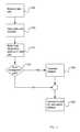
- FIG. 1is a block diagram of a switching environment.
- FIG. 2is a diagram of address domains.
- FIG. 3is a flow chart of a process for switching data units.
- the switching environmentincludes a switch 110 and a number of end points 120 a , 120 b , 120 c , 120 d .
- the switching environment 100may be a point-to-point communications network.
- switchmeans a system element that logically connects two or more ports to allow data units to be routed from one port to another, and the switch 110 is a switch.
- the switchroutes data units using memory-mapped I/O or I/O-mapped I/O (both, collectively, “mapped I/O”).
- the switch 110further includes a buffer 115 and logic 117 .
- the switch 110includes a number of ports 112 a , 112 b , 112 c , 112 d , which are physical interfaces between the buffer 115 and logic 117 and the end points 120 .
- data unitit is meant a frame, cell, datagram, packet or other unit of information. In some embodiments, such as PCI, a data unit is unencapsulated. Data units may be stored in the buffer 115 .
- bufferit is meant a dedicated or shared memory, a group or pipeline of registers, and/or other storage device or group of storage devices which can store data temporarily.
- the buffer 115may operate at a speed commensurate with the communication speed of the switching environment 100 . For example, it may be desirable to provide a dedicated memory for individual portions (as described below) and pipelined registers for multicast portions (as described below).
- the logic 117includes software and/or hardware for providing functionality and features described herein.
- the logic 117may include one or more of: logic arrays, memories, analog circuits, digital circuits, software, firmware, and processors such as microprocessors, field programmable gate arrays (FPGAs), application specific integrated circuits (ASICs), programmable logic devices (PLDs) and programmable logic arrays (PLAs).
- the hardware and firmware components of the logic 117may include various specialized units, circuits, software and interfaces for providing the functionality and features described herein.
- the inventionmay be embodied in whole or in part in software which operates in the switch 110 and may be in the form of firmware, an application program, an applet (e.g., a Java applet), a browser plug-in, a COM object, a dynamic linked library (DLL), a script, one or more subroutines, or an operating system component or service.
- the hardware and software of the invention and its functionsmay be distributed such that some components are performed by the switch 110 and others by other devices.
- the end points 120 a , 120 b , 120 c , 120 dare logical devices which connect to and communicate with the switch 110 respectively through the ports 112 . At least some of the end points may share an address domain, such as a memory address domain or an I/O address domain.
- address domainmeans the total range of addressable locations. If the shared address domain is a memory address domain, then data units are transmitted via memory mapped I/O to a destination address into the shared memory address domain.
- the end points 120may be connected to the ports 112 by electrical contacts, wirelessly, optically or otherwise.
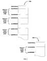
- FIG. 2there is shown a diagram of two address domains 200 , 250 .
- One address domain 200is shared by end points 120 a , 120 b , 120 d
- the other address domain 250is not shared and used only by end point 120 d . This is just an example; there may be more than two address domains, and more than one address domain may be shared.
- the address domains 200 , 250are contiguous ranges. Each address domains is defined by a master end point. Address portions associated with the individual end points 120 may be non-contiguous and the term “portions” is meant to refer to contiguous and non-contiguous spaces.
- the master end point for a given address domainallocates address portions to the other end points which share that address domain. The end points communicate their address space needs to the master device, and the master device allocates address space accordingly.
- Data unitsmay be written into or communicated into an address portion.
- address portions in a 32-bit shared memory address domain or shared I/O address domainwill be at least as large as the largest expected transaction, and comparable to those shown in FIG. 2 .
- separate address portions 210 a , 210 b , 210 cmay be associated with the corresponding end points 120 a , 120 b , 120 c .
- the address domain 200may be allocated so as to provide the corresponding end points 120 a , 120 b , 120 c with unique address portions.
- the address portionsmay be unique within the shared address domain 200 with respect to one another.
- non-shared address domain 250there may be a portion 250 d associated with the end point 120 d .
- the non-shared address domain 250is considered isolated from the shared address domain 210 .
- Other non-shared address domainscould be included, and they would also be considered isolated from the shared address domain, and from each other.
- isolatedit is meant that the address domains are separated such that interaction does not directly take place between them, and therefore uniquely addressable addresses are provided.
- the address portions 210may have various characteristics.
- the address portions 210may have respective sizes. The sizes may be fixed or variable.
- the address portions 210may be defined by a base address, as well as by a size or end address.
- the address portions 210may come to be associated with the end points 120 through an arbitrage process, through centralized assignment (e.g., by a host or the switch 110 ), otherwise or through a combination of these.
- the address portion 210 for a given end point 120need not be contiguous. To avoid errors, it may be desirable if the address portions 210 within the same address domain do not overlap.
- Data unitsmay be directed to one or more of the end points 120 by addressing. That is, a destination address is associated with and may be included in the data units. The destination address determines which end point 120 should receive a given data unit. Thus, data units addressed to the individual portion for a given end point 120 should be received only by that end point 120 . Depending on the embodiment, the destination address may be the same as the base address or may be within the address portion.
- the end points 120may be associated with respective ports 112 . Through this association, a given end point 120 may send data units to and receive data units from its associated port 112 . This association may be on a one-to-one basis. Because of these relationships, the ports 112 also have associations with the address portions 210 of the end points 120 . Thus, the ports 112 may be said to have address portions 210 within the address domains 200 , 250 .
- Ports within a shared addressed domainare considered “transparent”, and those not within a shared address domain are considered “non-transparent”. Data units from one transparent port to another may be transferred directly. However, data units between a transparent port and a non-transparent port require address translation to accommodate the differences in their respective address domains.
- Transparent portsare logical interfaces within a single addressing domain. Non-transparent ports allow interaction between completely separate addressing domains, but addresses from one domain must be converted from one domain to the other.
- the logic 117may allow designation on a port-by-port of transparency or non-transparency, including the address domain for a given port.
- the switch 110may be responsive to requests or instructions from the devices 120 to indicate such things as which address domain the devices will be in, and the address portion associated with a given device.
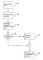
- FIG. 3there is shown a flow chart of a process for switching data units.
- the processemploys a switch having transparent and non-transparent ports, such as the switches described above.
- the transparent portsare associated with a shared address domain
- the non-transparent portsare associated with non-shared address domains.
- Domain maps for each address domainmay be communicated to the switch.
- a master end pointsuch as a processor, which is responsible for allocating address portions within its address domain. End points may communicate their address space needs to the master device, and the master device may allocate address space accordingly. The master device may query end points for their address space needs. These allocations, and other allocations and designations, define the address map which the master end point communicates to the switch.
- the switchmay receive a single communication of an address map from a master end point.
- the switchmay receive partial or revised address maps from time to time.
- a first step 305the switch receives a data unit.
- the switchthen stores the data unit in a buffer (step 310 ).
- the switchdetermines the destination address of the data unit (step 315 ).
- the switchdetermines whether the destination address is associated with a transparent or non-transparent port (step 325 ).
- the switchtranslates the address (step 330 ).
- Many different schemes of memory and I/O address translation for mapping from one address domain into anothermay be used. These schemes include direct memory translation both with and without offsets, and indirect memory translation through lookup registers or tables.
- addressesmay be translated using schemes other than address map translation, such as mailbox mechanisms and doorbell registers.
- the switchforwards the data unit to the port for the designated destination address (step 395 ).
- data unitsare transferred between the transparent ports, between the transparent and non-transparent ports, and between the non-transparent ports.
- non-transparent portsallow data transfers from one address domain to another.
- the switchis a PCI Express switch in which one or more of the interfaces (i.e., ports) are optionally non-transparent.
- a device connected to a non-transparent port of the switchis isolated from the address domain of the other ports on the switch.
- Two or more processors with their own address mapscould all communicate with each other through this type of PCI Express switch.
- Non-transparent operationallows a local subsystem to maintain a full address range completely separate from the main system.
- the presence of the local busis obfuscated from the main system by presenting the non-transparent bridge as an endpoint.
- Bus enumeration and discovery softwareremains unaware of the presence of the secondary local bus, allowing for a higher level of abstraction at the system level.
- a transparent bridgemay be associated with a different type of configuration space than a non-transparent bridge.
- bus enumeration and discovery softwaremay read “through” the bridge device in an attempt to identify additional downstream devices.
- a non-transparent bridgemasks the presence of the secondary local bus by identifying itself as an endpoint. The endpoint association is made via a non-transparent type configuration header.
- bus enumeration and discovery softwareis satisfied and does not attempt to read through the non-transparent bridge.
- a PCI Express switch(including a bridge as described herein) in non-transparent mode allows completely independent and unrestricted address ranges to exist on both sides of the bridge. Transactions passing through the bridge will have their addresses remapped to a correlating destination address.
- a local host processormay be responsible for maintaining address translation and configuration registers. When address configuration is complete, a primary side lockout bit may “wake” the primary PCI Express endpoint interface, allowing it to respond to bus discovery queries.
- Addressesmay be remapped in a three-stage process.
- the size and configuration of each address base address rangeis set by the local host. This allows software agents on the main host to allocate and distribute the main memory map.
- the local hostprograms the translation offset.
- software agents on each side of the bridgeperform standard PCI address mapping techniques to map the respective address regions into system memory space.
- a translation functionUpon receiving a transaction that falls within a given base address range, a translation function overwrites the upper bits of the address with the translated base offset, or some other address translation technique. Thus, separate address ranges are maintained on both sides of the non-transparent bridge.
- a downstream rangemay be associated with requests moving from the PCI Express to the PCI interface.
- An upstream rangeis associated with request moving from the local PCI bus to the PCI Express interface.
Landscapes
- Engineering & Computer Science (AREA)
- Computer Networks & Wireless Communication (AREA)
- Signal Processing (AREA)
- Computer Hardware Design (AREA)
- Theoretical Computer Science (AREA)
- Software Systems (AREA)
- Physics & Mathematics (AREA)
- General Engineering & Computer Science (AREA)
- General Physics & Mathematics (AREA)
- Multi Processors (AREA)
Abstract
Description
Claims (5)
Priority Applications (1)
| Application Number | Priority Date | Filing Date | Title |
|---|---|---|---|
| US12/894,003US7945722B2 (en) | 2003-11-18 | 2010-09-29 | Routing data units between different address domains |
Applications Claiming Priority (5)
| Application Number | Priority Date | Filing Date | Title |
|---|---|---|---|
| US52324603P | 2003-11-18 | 2003-11-18 | |
| US10/993,277US7454552B2 (en) | 2003-11-18 | 2004-11-18 | Switch with transparent and non-transparent ports |
| US11/031,853US7421532B2 (en) | 2003-11-18 | 2005-01-06 | Switching with transparent and non-transparent ports |
| US12/195,122US7814259B2 (en) | 2003-11-18 | 2008-08-20 | PCI express switch with backwards compatibility |
| US12/894,003US7945722B2 (en) | 2003-11-18 | 2010-09-29 | Routing data units between different address domains |
Related Parent Applications (1)
| Application Number | Title | Priority Date | Filing Date |
|---|---|---|---|
| US12/195,122ContinuationUS7814259B2 (en) | 2003-11-18 | 2008-08-20 | PCI express switch with backwards compatibility |
Publications (2)
| Publication Number | Publication Date |
|---|---|
| US20110016258A1 US20110016258A1 (en) | 2011-01-20 |
| US7945722B2true US7945722B2 (en) | 2011-05-17 |
Family
ID=46303664
Family Applications (3)
| Application Number | Title | Priority Date | Filing Date |
|---|---|---|---|
| US11/031,853Active2026-08-05US7421532B2 (en) | 2003-11-18 | 2005-01-06 | Switching with transparent and non-transparent ports |
| US12/195,122Expired - LifetimeUS7814259B2 (en) | 2003-11-18 | 2008-08-20 | PCI express switch with backwards compatibility |
| US12/894,003Expired - Fee RelatedUS7945722B2 (en) | 2003-11-18 | 2010-09-29 | Routing data units between different address domains |
Family Applications Before (2)
| Application Number | Title | Priority Date | Filing Date |
|---|---|---|---|
| US11/031,853Active2026-08-05US7421532B2 (en) | 2003-11-18 | 2005-01-06 | Switching with transparent and non-transparent ports |
| US12/195,122Expired - LifetimeUS7814259B2 (en) | 2003-11-18 | 2008-08-20 | PCI express switch with backwards compatibility |
Country Status (1)
| Country | Link |
|---|---|
| US (3) | US7421532B2 (en) |
Cited By (4)
| Publication number | Priority date | Publication date | Assignee | Title |
|---|---|---|---|---|
| US20110238909A1 (en)* | 2010-03-29 | 2011-09-29 | Pankaj Kumar | Multicasting Write Requests To Multiple Storage Controllers |
| US20150261709A1 (en)* | 2014-03-14 | 2015-09-17 | Emilio Billi | Peripheral component interconnect express (pcie) distributed non- transparent bridging designed for scalability,networking and io sharing enabling the creation of complex architectures. |
| US9910816B2 (en)* | 2013-07-22 | 2018-03-06 | Futurewei Technologies, Inc. | Scalable direct inter-node communication over peripheral component interconnect-express (PCIe) |
| US11681646B1 (en) | 2022-02-16 | 2023-06-20 | Drut Technologies Inc. | Memory disaggregation and reallocation |
Families Citing this family (37)
| Publication number | Priority date | Publication date | Assignee | Title |
|---|---|---|---|---|
| US7454552B2 (en)* | 2003-11-18 | 2008-11-18 | Topside Research, Llc | Switch with transparent and non-transparent ports |
| US7421532B2 (en)* | 2003-11-18 | 2008-09-02 | Topside Research, Llc | Switching with transparent and non-transparent ports |
| US20080301328A1 (en)* | 2004-04-27 | 2008-12-04 | Russ Craig F | Method and system for improved communication between central processing units and input/output processors |
| US7058738B2 (en)* | 2004-04-28 | 2006-06-06 | Microsoft Corporation | Configurable PCI express switch which allows multiple CPUs to be connected to multiple I/O devices |
| US7685319B2 (en) | 2004-09-28 | 2010-03-23 | Cray Canada Corporation | Low latency communication via memory windows |
| US20060282602A1 (en)* | 2005-06-09 | 2006-12-14 | Tse-Hsine Liao | Data transmission device and method thereof |
| US7546574B2 (en)* | 2005-12-02 | 2009-06-09 | Gauda, Inc. | Optical proximity correction on hardware or software platforms with graphical processing units |
| JP4877482B2 (en)* | 2006-04-11 | 2012-02-15 | 日本電気株式会社 | PCI Express link, multi-host computer system, and PCI Express link reconfiguration method |
| US20080052403A1 (en)* | 2006-08-23 | 2008-02-28 | Sun Microsystems, Inc. | Input/output routers with dual internal ports |
| US7594060B2 (en)* | 2006-08-23 | 2009-09-22 | Sun Microsystems, Inc. | Data buffer allocation in a non-blocking data services platform using input/output switching fabric |
| US7676625B2 (en)* | 2006-08-23 | 2010-03-09 | Sun Microsystems, Inc. | Cross-coupled peripheral component interconnect express switch |
| US20080123677A1 (en)* | 2006-08-31 | 2008-05-29 | Honeywell International Inc. | System management bus port switch |
| US7519761B2 (en)* | 2006-10-10 | 2009-04-14 | International Business Machines Corporation | Transparent PCI-based multi-host switch |
| US8122171B2 (en)* | 2009-03-20 | 2012-02-21 | National Instruments Corporation | Bus enumeration in a system with multiple buses |
| JP5318223B2 (en) | 2009-04-06 | 2013-10-16 | 株式会社日立製作所 | Storage subsystem and control method thereof |
| US8463934B2 (en)* | 2009-11-05 | 2013-06-11 | Rj Intellectual Properties, Llc | Unified system area network and switch |
| US8359401B2 (en)* | 2009-11-05 | 2013-01-22 | RJ Intellectual Properties, Inc. | Network switch |
| EP2698723A1 (en) | 2010-03-11 | 2014-02-19 | Ricoh Company, Ltd. | Adapter and communication method |
| JP5764919B2 (en)* | 2010-12-16 | 2015-08-19 | 株式会社リコー | Communication device and communication system |
| US8606984B2 (en)* | 2010-04-12 | 2013-12-10 | International Busines Machines Corporation | Hierarchical to physical bus translation |
| US8868804B2 (en) | 2010-10-20 | 2014-10-21 | Marvell World Trade Ltd. | Unified I/O adapter |
| US8725923B1 (en)* | 2011-03-31 | 2014-05-13 | Emc Corporation | BMC-based communication system |
| CN102393838B (en)* | 2011-07-04 | 2015-03-11 | 华为技术有限公司 | Data processing method and device, PCI-E (peripheral component interface-express) bus system, and server |
| RU2461055C1 (en)* | 2011-07-13 | 2012-09-10 | Федеральное государственное унитарное предприятие "Научно-исследовательский институт "Квант" | Cluster system with direct channel switching |
| US8943257B2 (en)* | 2011-09-30 | 2015-01-27 | Intel Corporation | Protocol neutral fabric |
| US8868672B2 (en)* | 2012-05-14 | 2014-10-21 | Advanced Micro Devices, Inc. | Server node interconnect devices and methods |
| TW201351930A (en)* | 2012-06-04 | 2013-12-16 | Accusys Inc | Switch system and method of operating switch |
| US9137173B2 (en) | 2012-06-19 | 2015-09-15 | Advanced Micro Devices, Inc. | Devices and methods for interconnecting server nodes |
| US8930595B2 (en) | 2012-06-21 | 2015-01-06 | Advanced Micro Devices, Inc. | Memory switch for interconnecting server nodes |
| US9253287B2 (en) | 2012-08-20 | 2016-02-02 | Advanced Micro Devices, Inc. | Speculation based approach for reliable message communications |
| US8875256B2 (en) | 2012-11-13 | 2014-10-28 | Advanced Micro Devices, Inc. | Data flow processing in a network environment |
| US20150113314A1 (en)* | 2013-07-11 | 2015-04-23 | Brian J. Bulkowski | Method and system of implementing a distributed database with peripheral component interconnect express switch |
| US9519606B2 (en)* | 2013-07-22 | 2016-12-13 | GigaIO Networks, Inc. | Network switch |
| US9336173B1 (en) | 2013-12-20 | 2016-05-10 | Microsemi Storage Solutions (U.S.), Inc. | Method and switch for transferring transactions between switch domains |
| US9419918B2 (en)* | 2014-11-07 | 2016-08-16 | Futurewei Technologies, Inc. | Non-transparent bridge method and apparatus for configuring high-dimensional PCI-express networks |
| US11456855B2 (en)* | 2019-10-17 | 2022-09-27 | Arm Limited | Obfuscating data at-transit |
| US11606299B2 (en)* | 2020-06-30 | 2023-03-14 | Viettel Group | Method for reducing impact of flapping links on performance of network devices |
Citations (51)
| Publication number | Priority date | Publication date | Assignee | Title |
|---|---|---|---|---|
| US4330824A (en) | 1978-08-17 | 1982-05-18 | Compagnie Internationale Pour L'informatique Cii Honeywell Bull (Societe Anonyme) | Universal arrangement for the exchange of data between the memories and the processing devices of a computer |
| US4394725A (en) | 1973-11-30 | 1983-07-19 | Compagnie Honeywell Bull | Apparatus and method for transferring information units between processes in a multiprocessing system |
| US4704606A (en) | 1984-11-13 | 1987-11-03 | American Telephone And Telegraph Company And At&T Information Systems Inc. | Variable length packet switching system |
| US4958299A (en) | 1988-06-13 | 1990-09-18 | Fuji Xerox Co., Ltd. | Control device for use with a drawing output unit |
| US5550823A (en) | 1994-04-28 | 1996-08-27 | Nec Corporation | Method and apparatus for performing priority control for cells in output buffer type ATM switch |
| US5555543A (en) | 1995-01-03 | 1996-09-10 | International Business Machines Corporation | Crossbar switch apparatus and protocol |
| US5617421A (en) | 1994-06-17 | 1997-04-01 | Cisco Systems, Inc. | Extended domain computer network using standard links |
| US5649149A (en) | 1994-08-01 | 1997-07-15 | Cypress Semiconductor Corporation | Integrated content addressable memory array with processing logical and a host computer interface |
| US5659713A (en) | 1992-04-24 | 1997-08-19 | Digital Equipment Corporation | Memory stream buffer with variable-size prefetch depending on memory interleaving configuration |
| US5841874A (en) | 1996-08-13 | 1998-11-24 | Motorola, Inc. | Ternary CAM memory architecture and methodology |
| US5860085A (en) | 1994-08-01 | 1999-01-12 | Cypress Semiconductor Corporation | Instruction set for a content addressable memory array with read/write circuits and an interface register logic block |
| US5898689A (en) | 1992-12-04 | 1999-04-27 | Lucent Technologies Inc. | Packet network interface |
| US5905911A (en) | 1990-06-29 | 1999-05-18 | Fujitsu Limited | Data transfer system which determines a size of data being transferred between a memory and an input/output device |
| US5923893A (en) | 1997-09-05 | 1999-07-13 | Motorola, Inc. | Method and apparatus for interfacing a processor to a coprocessor |
| US5961626A (en) | 1997-10-10 | 1999-10-05 | Motorola, Inc. | Method and processing interface for transferring data between host systems and a packetized processing system |
| US5982749A (en) | 1996-03-07 | 1999-11-09 | Lsi Logic Corporation | ATM communication system interconnect/termination unit |
| US6067408A (en) | 1993-05-27 | 2000-05-23 | Advanced Micro Devices, Inc. | Full duplex buffer management and apparatus |
| US6122674A (en) | 1997-07-10 | 2000-09-19 | International Business Machines Corporation | Bi-directional network adapter for interfacing local node of shared memory parallel processing system to multi-stage switching network for communications with remote node |
| US6138185A (en)* | 1998-10-29 | 2000-10-24 | Mcdata Corporation | High performance crossbar switch |
| US6172927B1 (en) | 1997-04-01 | 2001-01-09 | Ramtron International Corporation | First-in, first-out integrated circuit memory device incorporating a retransmit function |
| US6292878B1 (en) | 1996-12-12 | 2001-09-18 | Matsushita Electric Industrial Co., Ltd. | Data recorder and method of access to data recorder |
| US20010037435A1 (en) | 2000-05-31 | 2001-11-01 | Van Doren Stephen R. | Distributed address mapping and routing table mechanism that supports flexible configuration and partitioning in a modular switch-based, shared-memory multiprocessor computer system |
| US6346946B1 (en) | 1998-10-23 | 2002-02-12 | Micron Technology, Inc. | Graphics controller embedded in a core logic unit |
| US6389489B1 (en) | 1999-03-17 | 2002-05-14 | Motorola, Inc. | Data processing system having a fifo buffer with variable threshold value based on input and output data rates and data block size |
| US20020061022A1 (en) | 1999-08-27 | 2002-05-23 | Allen James Johnson | Network switch using network processor and methods |
| US20020099855A1 (en) | 1999-08-27 | 2002-07-25 | Brian Mitchell Bass | Network processor, memory organization and methods |
| US20020114326A1 (en) | 2001-02-16 | 2002-08-22 | Rupaka Mahalingaiah | Address mapping mechanism enabling multi-domain addressing in communication networks |
| US6442674B1 (en) | 1998-12-30 | 2002-08-27 | Intel Corporation | Method and system for bypassing a fill buffer located along a first instruction path |
| US20020122386A1 (en) | 2001-03-05 | 2002-09-05 | International Business Machines Corporation | High speed network processor |
| US6477623B2 (en) | 1998-10-23 | 2002-11-05 | Micron Technology, Inc. | Method for providing graphics controller embedded in a core logic unit |
| US20020165947A1 (en) | 2000-09-25 | 2002-11-07 | Crossbeam Systems, Inc. | Network application apparatus |
| US6493347B2 (en) | 1996-12-16 | 2002-12-10 | Juniper Networks, Inc. | Memory organization in a switching device |
| US20020188754A1 (en) | 2001-04-27 | 2002-12-12 | Foster Michael S. | Method and system for domain addressing in a communications network |
| US6510138B1 (en) | 1999-02-25 | 2003-01-21 | Fairchild Semiconductor Corporation | Network switch with head of line input buffer queue clearing |
| US6557053B1 (en) | 2000-01-04 | 2003-04-29 | International Business Machines Corporation | Queue manager for a buffer |
| US20030084373A1 (en) | 2001-11-01 | 2003-05-01 | Sun Microsystems, Inc. | Method and apparatus for arbitrating transactions between domains in a computer system |
| US20030084219A1 (en) | 2001-10-26 | 2003-05-01 | Maxxan Systems, Inc. | System, apparatus and method for address forwarding for a computer network |
| US6574194B1 (en) | 1998-12-18 | 2003-06-03 | Cypress Semiconductor Corporation | Architecture of data communications switching system and associated method |
| US6611527B1 (en) | 1999-06-09 | 2003-08-26 | Hitachi, Ltd. | Packet switching apparatus with a common buffer |
| US20040019729A1 (en) | 2002-07-29 | 2004-01-29 | Kelley Richard A. | Buffer management and transaction control for transition bridges |
| US20040030857A1 (en) | 2002-07-31 | 2004-02-12 | Brocade Communications Systems, Inc. | Hardware-based translating virtualization switch |
| US6708262B2 (en) | 1997-02-11 | 2004-03-16 | Micron Technology, Inc. | Memory device command signal generator |
| US6714555B1 (en) | 1997-06-04 | 2004-03-30 | Roke Manor Research Limited | Broadband telecommunications switch |
| US6735219B1 (en) | 1998-09-10 | 2004-05-11 | International Business Machines Corporation | Packet-processing apparatus and packet switch adapter for the processing of variable-length packets and a method thereof |
| US20040123014A1 (en) | 2002-12-19 | 2004-06-24 | Intel Corporation | System and method for communicating over intra-hierarchy and inter-hierarchy links |
| US6795870B1 (en) | 2000-04-13 | 2004-09-21 | International Business Machines Corporation | Method and system for network processor scheduler |
| US20040230735A1 (en) | 2003-05-15 | 2004-11-18 | Moll Laurent R. | Peripheral bus switch having virtual peripheral bus and configurable host bridge |
| US20050117578A1 (en) | 2003-11-18 | 2005-06-02 | Heath Stewart | Switching with transparent and non-transparent ports |
| US20060010355A1 (en) | 2004-07-08 | 2006-01-12 | International Business Machines Corporation | Isolation of input/output adapter error domains |
| US7080190B2 (en) | 2002-05-30 | 2006-07-18 | Lsi Logic Corporation | Apparatus and method for providing transparent sharing of channel resources by multiple host machines |
| US7454552B2 (en) | 2003-11-18 | 2008-11-18 | Topside Research, Llc | Switch with transparent and non-transparent ports |
Family Cites Families (3)
| Publication number | Priority date | Publication date | Assignee | Title |
|---|---|---|---|---|
| DE19546789A1 (en)* | 1995-12-14 | 1997-06-19 | Siemens Ag | Process for recycling contaminated metal parts |
| US6393148B1 (en)* | 1999-05-13 | 2002-05-21 | Hewlett-Packard Company | Contrast enhancement of an image using luminance and RGB statistical metrics |
| JP3949369B2 (en)* | 2000-10-20 | 2007-07-25 | 三菱電機株式会社 | AC generator for vehicles |
- 2005
- 2005-01-06USUS11/031,853patent/US7421532B2/enactiveActive
- 2008
- 2008-08-20USUS12/195,122patent/US7814259B2/ennot_activeExpired - Lifetime
- 2010
- 2010-09-29USUS12/894,003patent/US7945722B2/ennot_activeExpired - Fee Related
Patent Citations (56)
| Publication number | Priority date | Publication date | Assignee | Title |
|---|---|---|---|---|
| US4394725A (en) | 1973-11-30 | 1983-07-19 | Compagnie Honeywell Bull | Apparatus and method for transferring information units between processes in a multiprocessing system |
| US4330824A (en) | 1978-08-17 | 1982-05-18 | Compagnie Internationale Pour L'informatique Cii Honeywell Bull (Societe Anonyme) | Universal arrangement for the exchange of data between the memories and the processing devices of a computer |
| US4704606A (en) | 1984-11-13 | 1987-11-03 | American Telephone And Telegraph Company And At&T Information Systems Inc. | Variable length packet switching system |
| US4958299A (en) | 1988-06-13 | 1990-09-18 | Fuji Xerox Co., Ltd. | Control device for use with a drawing output unit |
| US5905911A (en) | 1990-06-29 | 1999-05-18 | Fujitsu Limited | Data transfer system which determines a size of data being transferred between a memory and an input/output device |
| US5659713A (en) | 1992-04-24 | 1997-08-19 | Digital Equipment Corporation | Memory stream buffer with variable-size prefetch depending on memory interleaving configuration |
| US5898689A (en) | 1992-12-04 | 1999-04-27 | Lucent Technologies Inc. | Packet network interface |
| US6067408A (en) | 1993-05-27 | 2000-05-23 | Advanced Micro Devices, Inc. | Full duplex buffer management and apparatus |
| US5550823A (en) | 1994-04-28 | 1996-08-27 | Nec Corporation | Method and apparatus for performing priority control for cells in output buffer type ATM switch |
| US5617421A (en) | 1994-06-17 | 1997-04-01 | Cisco Systems, Inc. | Extended domain computer network using standard links |
| US5649149A (en) | 1994-08-01 | 1997-07-15 | Cypress Semiconductor Corporation | Integrated content addressable memory array with processing logical and a host computer interface |
| US5860085A (en) | 1994-08-01 | 1999-01-12 | Cypress Semiconductor Corporation | Instruction set for a content addressable memory array with read/write circuits and an interface register logic block |
| US5555543A (en) | 1995-01-03 | 1996-09-10 | International Business Machines Corporation | Crossbar switch apparatus and protocol |
| US5982749A (en) | 1996-03-07 | 1999-11-09 | Lsi Logic Corporation | ATM communication system interconnect/termination unit |
| US5841874A (en) | 1996-08-13 | 1998-11-24 | Motorola, Inc. | Ternary CAM memory architecture and methodology |
| US6292878B1 (en) | 1996-12-12 | 2001-09-18 | Matsushita Electric Industrial Co., Ltd. | Data recorder and method of access to data recorder |
| US6493347B2 (en) | 1996-12-16 | 2002-12-10 | Juniper Networks, Inc. | Memory organization in a switching device |
| US6708262B2 (en) | 1997-02-11 | 2004-03-16 | Micron Technology, Inc. | Memory device command signal generator |
| US6172927B1 (en) | 1997-04-01 | 2001-01-09 | Ramtron International Corporation | First-in, first-out integrated circuit memory device incorporating a retransmit function |
| US6714555B1 (en) | 1997-06-04 | 2004-03-30 | Roke Manor Research Limited | Broadband telecommunications switch |
| US6122674A (en) | 1997-07-10 | 2000-09-19 | International Business Machines Corporation | Bi-directional network adapter for interfacing local node of shared memory parallel processing system to multi-stage switching network for communications with remote node |
| US5923893A (en) | 1997-09-05 | 1999-07-13 | Motorola, Inc. | Method and apparatus for interfacing a processor to a coprocessor |
| US5961626A (en) | 1997-10-10 | 1999-10-05 | Motorola, Inc. | Method and processing interface for transferring data between host systems and a packetized processing system |
| US6735219B1 (en) | 1998-09-10 | 2004-05-11 | International Business Machines Corporation | Packet-processing apparatus and packet switch adapter for the processing of variable-length packets and a method thereof |
| US6477623B2 (en) | 1998-10-23 | 2002-11-05 | Micron Technology, Inc. | Method for providing graphics controller embedded in a core logic unit |
| US6346946B1 (en) | 1998-10-23 | 2002-02-12 | Micron Technology, Inc. | Graphics controller embedded in a core logic unit |
| US6138185A (en)* | 1998-10-29 | 2000-10-24 | Mcdata Corporation | High performance crossbar switch |
| US6574194B1 (en) | 1998-12-18 | 2003-06-03 | Cypress Semiconductor Corporation | Architecture of data communications switching system and associated method |
| US6442674B1 (en) | 1998-12-30 | 2002-08-27 | Intel Corporation | Method and system for bypassing a fill buffer located along a first instruction path |
| US6510138B1 (en) | 1999-02-25 | 2003-01-21 | Fairchild Semiconductor Corporation | Network switch with head of line input buffer queue clearing |
| US6389489B1 (en) | 1999-03-17 | 2002-05-14 | Motorola, Inc. | Data processing system having a fifo buffer with variable threshold value based on input and output data rates and data block size |
| US6611527B1 (en) | 1999-06-09 | 2003-08-26 | Hitachi, Ltd. | Packet switching apparatus with a common buffer |
| US6842443B2 (en) | 1999-08-27 | 2005-01-11 | International Business Machines Corporation | Network switch using network processor and methods |
| US20020099855A1 (en) | 1999-08-27 | 2002-07-25 | Brian Mitchell Bass | Network processor, memory organization and methods |
| US20020061022A1 (en) | 1999-08-27 | 2002-05-23 | Allen James Johnson | Network switch using network processor and methods |
| US6557053B1 (en) | 2000-01-04 | 2003-04-29 | International Business Machines Corporation | Queue manager for a buffer |
| US6795870B1 (en) | 2000-04-13 | 2004-09-21 | International Business Machines Corporation | Method and system for network processor scheduler |
| US20010037435A1 (en) | 2000-05-31 | 2001-11-01 | Van Doren Stephen R. | Distributed address mapping and routing table mechanism that supports flexible configuration and partitioning in a modular switch-based, shared-memory multiprocessor computer system |
| US20020165947A1 (en) | 2000-09-25 | 2002-11-07 | Crossbeam Systems, Inc. | Network application apparatus |
| US20020114326A1 (en) | 2001-02-16 | 2002-08-22 | Rupaka Mahalingaiah | Address mapping mechanism enabling multi-domain addressing in communication networks |
| US20020122386A1 (en) | 2001-03-05 | 2002-09-05 | International Business Machines Corporation | High speed network processor |
| US6987760B2 (en) | 2001-03-05 | 2006-01-17 | International Business Machines Corporation | High speed network processor |
| US20020188754A1 (en) | 2001-04-27 | 2002-12-12 | Foster Michael S. | Method and system for domain addressing in a communications network |
| US20030084219A1 (en) | 2001-10-26 | 2003-05-01 | Maxxan Systems, Inc. | System, apparatus and method for address forwarding for a computer network |
| US20030084373A1 (en) | 2001-11-01 | 2003-05-01 | Sun Microsystems, Inc. | Method and apparatus for arbitrating transactions between domains in a computer system |
| US7080190B2 (en) | 2002-05-30 | 2006-07-18 | Lsi Logic Corporation | Apparatus and method for providing transparent sharing of channel resources by multiple host machines |
| US20040019729A1 (en) | 2002-07-29 | 2004-01-29 | Kelley Richard A. | Buffer management and transaction control for transition bridges |
| US20040030857A1 (en) | 2002-07-31 | 2004-02-12 | Brocade Communications Systems, Inc. | Hardware-based translating virtualization switch |
| US20040123014A1 (en) | 2002-12-19 | 2004-06-24 | Intel Corporation | System and method for communicating over intra-hierarchy and inter-hierarchy links |
| US7096305B2 (en) | 2003-05-15 | 2006-08-22 | Broadcom Corporation | Peripheral bus switch having virtual peripheral bus and configurable host bridge |
| US20040230735A1 (en) | 2003-05-15 | 2004-11-18 | Moll Laurent R. | Peripheral bus switch having virtual peripheral bus and configurable host bridge |
| US20050117578A1 (en) | 2003-11-18 | 2005-06-02 | Heath Stewart | Switching with transparent and non-transparent ports |
| US7421532B2 (en) | 2003-11-18 | 2008-09-02 | Topside Research, Llc | Switching with transparent and non-transparent ports |
| US7454552B2 (en) | 2003-11-18 | 2008-11-18 | Topside Research, Llc | Switch with transparent and non-transparent ports |
| US7814259B2 (en)* | 2003-11-18 | 2010-10-12 | Internet Machines, Llc | PCI express switch with backwards compatibility |
| US20060010355A1 (en) | 2004-07-08 | 2006-01-12 | International Business Machines Corporation | Isolation of input/output adapter error domains |
Non-Patent Citations (97)
| Title |
|---|
| Ajanovic, et al., 3GIO Protocol and Software Interface, Intel Corporation, Intel Developer Forum, Feb. 25-28, 2002, slides 1-27. |
| Akber Kazmi, Non-Transparent Bridging Makes PCI-Express HA Friendly, Aug. 14, 2003, http://www.eetimes.com/story/OEG20030814S0015. |
| Arapahoe, 3GIO Base Specification, Rev. 1.0, Release Candidate, Feb. 22, 2002, pp. 1-310. |
| Bhatt, Creating a Third Generation I/O Interconnect, White Paper, 2002, pp. 1-8, Technology and Research Labs, Intel Corporation, http://www.intel.com/technology/pciexpress/downloads/3rdgenwhitepaper.pdf. |
| Bob Davis, PEI-8 PCI Express AS Core, Network Appliance, Inc., Oct. 27, 2002. |
| Budruk, et al., PCI Express System Architecture, Library of Congress Catalog Record, LCCN Control No. 2003015461, book, Published in Boston, 2004. |
| Budruk, et al., PCI Express System Architecture, MindShare, Inc., PC System Architecture Series, Published on Sep. 4, 2003, Cover Page. |
| Budruk, et al., PCI Express System Architecture, MindShare, Inc., Published on Sep. 4, 2003, p. 132-133. |
| Budruk, et al., PCI Express System Architecture, MindShare, Inc., Published on Sep. 4, 2003, p. 42. |
| Budruk, et al., PCI Express System Architecture, MindShare, Inc., Published on Sep. 4, 2003, p. 48 and 50. |
| Budruk, et al., PCI Express System Architecture, MindShare, Inc., Published on Sep. 4, 2003, p. 48. |
| Budruk, et al., PCI Express System Architecture, MindShare, Inc., Published on Sep. 4, 2003, p. 54. |
| Business Wire, StarGen Unveils Plans for Future Communications Products; Will Demonstrate PIC 2.17 StarFabric Development Platform to Show the Capabilities of StarFabric in Communication Applications, Press Release, Article Date, Sep. 23, 2002, http://www.highbeam.com/doc/1G1-91910757.html. |
| Danny Chi et al. Utilizing Non-Transparent Bridign in PCI Express Base(TM) Create Multi Processor Systems, Part I, TechOnLine Webcast, Aug. 26, 2003, http://seminar2.techonline.com/~plx22/aug2603/index.shtml. |
| Danny Chi et al. Utilizing Non-Transparent Bridign in PCI Express Base™ Create Multi Processor Systems, Part I, TechOnLine Webcast, Aug. 26, 2003, http://seminar2.techonline.com/˜plx22/aug2603/index.shtml. |
| Danny Chi, Designing for Performance with PCI Express(TM), Feb. 25, 2003, PLX Technology, TechOnLine Webcast, http://seminar2.techonline.com/~plx22/feb2503/archive/blank.html. |
| Danny Chi, Designing for Performance with PCI Express™, Feb. 25, 2003, PLX Technology, TechOnLine Webcast, http://seminar2.techonline.com/˜plx22/feb2503/archive/blank.html. |
| Dodson, et al., Advanced Switching Makes PCI Express More Comms Friendly, EE/Times, News & Analysis, Dec. 12, 2002, http://www.eetimes.com/electronics-news/4143638/Advanced-Switching-Makes-PCI-Express-More-Comms-Friendly. |
| Dodson, et al., Advanced Switching Makes PCI Express More Comms Friendly, plx tECHNOLOGY, Dec. 12, 2002, http://www.eetimes.com/General/DisplayPrintViewContent?contentltemld=4143638. |
| eeProductCenter, CPCI Board Supports Multiprocessing, Feb. 2, 1999, http://www.eeproductcenter.com/showArticle.jhtml?articleID=15300408. |
| Fahmy, A Survey of ATM Switching Techniques, Aug. 14, 2001, Department of Computer and Information Science, The Ohio State University. |
| Gary Solomon, PCI Express-AS (Advanced Switching) Architecture Overview, AWG ExAS KD Event, Nov. 20, 2002, slides 1-28. |
| Gary Solomon, PCI Express—AS (Advanced Switching) Architecture Overview, AWG ExAS KD Event, Nov. 20, 2002, slides 1-28. |
| Gupta, Scheduling in Input Queued Switches: A Survey, Jun. 1996, Department of Computer Science, Stanford University, California. |
| HiNT Corporation, HiNT Corporation announces its advanced 66 MHz/64 Bit Universal, Dual Mode (Transparent or Non Transparent), Hot Swap Capable (Mid-Transaction Extraction Problem Eliminated) PCI/PCI bridge for embedded and high-end platforms, Mar. 13, 2002. |
| HiNT, HiNT HB6 Dual Mode Universal PCI-to-PCI Bridge, Datasheet, Rev. 1.0, Jan. 18, 2002, pp. 1-187. |
| Intel, 21554 Embedded PCI-to-PCI Bridge Hardware Implementation, Mar. 1999, Application Note, pp. 1-24. |
| Intel, 21554 Embedded PCI-to-PCI Bridge Performance Optimization, Sep. 1998, Application Note, pp. 1-13. |
| Intel, 21554 PCI-to-PCI Bridge for Embedded Applications, Dec. 1998, Product Preview Datasheet, pp. 1-52. |
| Intel, 21554 PCI-to-PCI Bridge, Sep. 2000, Specification Update, pp. 1-16. |
| Intel, 21555 Non-Transparent PCI-to-PCI Bridge, Sep. 2000, Specification Update, pp. 1-14. |
| Intel, 22 Industry Leaders Join Arapahoe Work Group as Key Developers, Intel Developer Forum, Intel Press Release, Aug. 29, 2001. |
| Intel, Improve Video Quality with the PCI Express x16 Graphics Interface, Sales Brief, 2004, pp. 1-2, Intel Corporation, http://www.intel.com/design/chipsets/pciexpress.pdf. |
| Intel, The Impact of Advanced Switching (AS), 2002, TechOnLine Webcast, http://seminar2.techonline.com/~intel22/oct2902/archive/userStart.html. |
| Intel, The Impact of Advanced Switching (AS), 2002, TechOnLine Webcast, http://seminar2.techonline.com/˜intel22/oct2902/archive/userStart.html. |
| Jack Regula, Using Non-Transparent Bridging in PCI Express Systems, PLX Technology Inc., Jun. 1, 2004, pp. 1-31. |
| Jack Regula, Using Non-Transparent Bridging in PCI Express Systems, PLX Technology, Inc., Jun. 1, 2004, pp. 1-31. |
| Jack Regula, Utilizing Non-Transparent Bridging in PCI Express Base to Create Multi-Processor Systems, Part II, Oct. 21, 2003, PLX Technology, TechOnLine Webcast, http://seminar2.techonline.com/~plx22/oct2103/archive/userStart.html?audio=0. |
| Jack Regula, Utilizing Non-Transparent Bridging in PCI Express Base to Create Multi-Processor Systems, Part II, Oct. 21, 2003, PLX Technology, TechOnLine Webcast, http://seminar2.techonline.com/˜plx22/oct2103/archive/userStart.html?audio=0. |
| Jack Regula, Utilizing Non-Transparent Bridign in PCI Express Base(TM) to Create Multi Processor Systems, Part II, TechOnLine Webcast, Oct. 21, 2003, http://seminar2.techonline.com/~plx22/oct2103/index.shtml. |
| Jack Regula, Utilizing Non-Transparent Bridign in PCI Express Base™ to Create Multi Processor Systems, Part II, TechOnLine Webcast, Oct. 21, 2003, http://seminar2.techonline.com/˜plx22/oct2103/index.shtml. |
| Jerry Ascierto, Intel Details Next-Generation I/O Spec, EE/Times, News & Analysis, Aug. 30, 2001, http://www.eetimes.com/electronics-news/4166991/Intel-details-next-generation-I-O-spec. |
| Jerry Steach, PLX Technology Announces PCI Express Collaboration with Catalyst Enterprises, Press Release, Jan. 15, 2004, http://www.plxtech.com/about/news/pr/2004/0115. |
| John Beaton, EID 2002-2003 Demo Plan for PCI Express, May 2002, slides 1-33. |
| John Gudmundson, Enabling Multi-Host System Designs with PCI Express Technology, May 2004, PLX Technology, Tech Feature, PCI Express, pp. 1-5. |
| John Gudmundson, Enabling Multi-Host System Designs with PCI Express Technology, May 2004, PLX Technology, TechFeature, PCI Express, Article. |
| Klein, PCI Express Is the new I/O Solution of Choice, Article, Nov. 2004, pp. 1-5, Technology @ Intel Magazine, Intel Corporation. |
| Loring Wirbel, StarFabric Association Joins Forces with PCI Group, Aug. 12, 2002, EE/Times, News & Analysis, http://www.eetimes.com/electronics-news/4142846/StarFabric-association-joins-forces-with-PCI-group. |
| Mark Hachman, Intel Reveals Details of Arapahoe/3GIO After SIG Approval, Technology News by ExtremeTech, Aug. 3, 2001, http://www.extremetech.com/article2/0,2845,118922,00.asp. |
| Mayhew et al., PCI Express and Advanced Switching: Evolutionary Path to Building Next Generation Interconnects, Proceedings of 11th Symposim on High Performance Interconnects, Aug. 20, 2003, pp. 21-29, IEEE, Piscataway, NJ. |
| MindShare, Inc., MindShare, Inc. Announces Publication of PCI Express System Architecture, Press Release, Aug. 20, 2003, http://www.plxtech.com/about/news/pr/2003/0820. |
| Nicolas Mokhoff, PLX to Specify 3GIO Silicon, Jan. 22, 2002, EE/Times, News & Analysis, http://www.eetimes.com/electronics-news/4141424/PLX-to-specify-3GIO-silicon. |
| PCI Express, PCT Express(TM) Base Specification Revision 1.0, Jul. 22, 2002, pp. 1-422. |
| PCI Express, PCT Express(TM) Base Specification Revision 1.0a, Apr. 15, 2003, pp. 1-428. |
| PCI Express, PCT Express™ Base Specification Revision 1.0, Jul. 22, 2002, pp. 1-422. |
| PCI Express, PCT Express™ Base Specification Revision 1.0a, Apr. 15, 2003, pp. 1-428. |
| PCI-SIG, 22 Industry Leaders Join Arapahoe Work Group as Key Developers, Intel Developer Forum, News Release, Aug. 29, 2001. |
| PCI-SIG, Compaq, Dell, IBM, Intel and Microsoft Work Jointly with PCI-SIG to Create Open Specification for Next General-Purpose I/O, News Release, Aug. 3, 2001. |
| Petaswitch Solutions, Inc., Company Overview, 2001, http://www.peta-switch.com/markets/overview.htm. |
| Petaswitch Solutions, Inc., PetaSwitch Solutions Announces Raising $4 Million in First Round Financing, Press Release, 2001, http://peta-switch.com/newsroom/press-releases.htm. |
| Petaswitch Solutions, Inc., PetaSwitch Solutions Announces Raising $4 Million in First Round Financing, Press Release, 2001, http://peta-switch.com/newsroom/press—releases.htm. |
| Petaswitch Solutions, Inc., The Pisces Chipset, Product Brief, 2001, http://www-peta-switch.com/products/product-brief.htm. |
| Petaswitch Solutions, Inc., The Pisces Chipset, Product Brief, 2001, http://www-peta-switch.com/products/product—brief.htm. |
| PLX Technology, Inc., New PLX PCI Express, PCI, PCI-X Technologies Tested at PCI-SIG Compliance Workshop, Press Release, Mar. 17, 2004, http://www.plxtech.com/about/news/pr/2004/0317. |
| PLX Technology, Inc., PLX Announces Development of I/O Interconnect Devices Based on PCI Express Technology, Press Release, Aug. 19, 2002, http://www.plxtech.com/about/news/pr/2002/0819. |
| PLX Technology, Inc., PLX Demonstrate Digital Imaging Over PCI Express Technology, Press Release, Feb. 17, 2004, http://www.plxtech.com/about/news/pr/2004/0217. |
| PLX Technology, Inc., PLX Joins Intel Developer Network for PCI Express Technology, Press Release, Sep. 9, 2002, http://www.plxtech.com/about/news/pr/2002/0909. |
| PLX Technology, Inc., PLX Provide In-Depth Webcast Oct. 21 on Implementing PCI Express in Multiprocessor Systems, Press Release, Oct. 14, 2003, http://www.plxtech.com/about/news/pr/2003/1014. |
| PLX Technology, Inc., PLX Reaches New Milestone in PCI Express, Press Release, Oct. 26, 2004, http://www.plxtech.com/about/news/pr/2004/1026. |
| PLX Technology, Inc., PLX Showcases I/O Interconnect Expertise in Live Demonstrations, Technical-Session Tutorial, Press Release, Sep. 7, 2004, http://www.plxtech.com/about/news/pr/2004/0907. |
| PLX Technology, Inc., PLX Technology Announces Broad PCI Express Interconnect Family Based on Unique Architecture, Press Release, Jan. 14, 2003, http://www.plxtech.com/about/news/pr/2003/0114. |
| PLX Technology, Inc., PLX Technology Announces First Controller Based on New Switch Fabric Architecture, Press Release, Mar. 26, 2001, http://www.plxtechnology.com/about/news/pr/2001/0326. |
| PLX Technology, Inc., PLX Technology Announces Industry's Smallest PCI Express Bridge Chip, Press Release, Jun. 8, 2004, http://www.plxtech.com/about/news/pr/2004/0608. |
| PLX Technology, Inc., PLX Technology Announces PCI Express Collaboration with Catalysis Enterprises, Press Release Jan. 15, 2004, http://www.plxtech.com/about/news/pr/2004/0115. |
| PLX Technology, Inc., PLX Technology Online Seminar to Instruct System Design Community on How to Implement PCI Express Multiprocessor Applications, Press Release, Aug. 22, 2003, http://www.plxtech.com/about/news/pr12003/0822. |
| PLX Technology, Inc., PLX Technology to Deliver In-Depth PCI Express Seminar in TechOnline Webcast, Press Release, Feb. 19, 2003, http://www.plxtech.com/about/news/pr/2003/0219. |
| PLX Technology, Inc., PLX Technology to Deliver Third In-Depth PCI Express Seminar in TechOnline Webcast, Press Release, Mar. 18, 2003, http://www.plxtech.com/about/news/pr/2003/0318. |
| PLX Technology, Inc., PLX to Showcase First PCT Express* Emulation at IDF, Press Release, Sep. 2, 2003. |
| PLX Technology, Inc., PLX to Test PCI Express Technology at PCI-SIG Compliance Workshop, Press Release, Dec. 9, 2003, http://www.plxtech.com/about/news/pr/2003/1209. |
| PLX Technology, Inc., PLX, MindShare to Deliver Second Comprehensive PCI Express Technical Seminar, Press Release, Jun. 9, 2004, http://www.plxtech.com/about/news/pr/2004/0609. |
| PLX Technology, Inc., PLX, Technology Announces Industry's Most Complee GFlexible Line of PCI Express Switches, Bridges, Press Release, Apr. 19, 2004, http://www.plxtech.com/about/news/pr/2004/0419. |
| PLX Technology, PLX Technology Announces First Controller Based on New Switch Fabric Architecture, Press Release, Mar. 26, 2001, http://www.plxtech.com/about/news/pr/2001/0326. |
| Ramin Neshati, PCI Express * (formerly 3GIO) Specification Ready for Use in Early Designs, Intel Developer Update Magazine, Jul. 2002, pp. 1-4. |
| Ray Weiss, 3GIO Named Successor to PCI/PCI-X, Oct. 29, 2001, Electronic Design, http://electronicdesign.com/article/embedded/3gio-named-successor-to-pci-pci-x3583.aspx. |
| Ray Weiss, Serialized PCI: The Next Bus Link, Jun. 21, 2000, EE/Times, News & Analysis, http://www.eetimes.com/electronics-news/4197032/Serialized-PCI-The-Next-Bus-Link. |
| Regula, et al., Using Non-Transparent Bridging in PCI Express Systems, Sep. 10, 2003, PLX Technology, Inc., pp. 1-31. |
| Rick Merritt, PCI Group Takes Express to Comms OEMs, Jul. 23, 2003, EE/Times, News & Analysis, http://www.eetimes.com/electronics-news/4138926/PCI-group-takes-Express-to-comms-OEMs-item-1. |
| Sarpa, et al., How HyperTransport and PCI Express Complement Each Other, EE/Times, News & Analysis, Dec. 23, 2002, http://www.eetimes.com/electronics-news/4143202/How-HyperTransport-and-PCI-Express-complement-each-other. |
| Schoenen, et al, Distributed Cell Scheduling Algorithms for Virtual-Output-Queued Switches, Dec. 1999, pp. 1211-1215, vol. 1, Globecom, IEEE Global Telecommunications Conference. |
| Stam, Inside PCI Express, Article, Sep. 9, 2002, pp. 1-37, ExtremeTech, http://www.extremetech.com/article2/0,3973,522663,00.asp. |
| Stephen Shankland, Analysts Say Intel Proposal Could Split PC Industry, CNET News, Mar. 1, 2001, http://news.cnetcom/2100-1001-253420.html. |
| Stephen Shankland, Approval Near on Intel PC-Overhaul Plan, ZD Net, CNET News on Jul. 31, 2001, http://www.zdnetasia.com/approval-near-on-intel-pc-overhaul-plan-20098955.htm. |
| Stephen Shankland, Intel, AMD Square Off Over Standard, Jul. 25, 2001, CNET News, http://news.cnet.com/2100-1001-270578.html. |
| Stiliadis, et al., Rate-Proportional Servers: A Design Methodology for Fair Queueing Algorithms, Dec. 1995, Computer Engineering & Information Sciences, University of California, Santa Cruz. |
| Stoica, et al., Earliest Eligible Virtual Deadline First: A Flexible and Accurate Mechanism for Proportional Share Resource Allocation, Department of Computer Science, Old Dominion University, Norfolk, VA. |
| Tommy Lee, PCI Express(TM) Design Enablement Efforts Accelerate Initial Product Testing in Early 2003. News Release, Nov. 19, 2002. |
| Tommy Lee, PCI Express™ Design Enablement Efforts Accelerate Initial Product Testing in Early 2003. News Release, Nov. 19, 2002. |
Cited By (10)
| Publication number | Priority date | Publication date | Assignee | Title |
|---|---|---|---|---|
| US20110238909A1 (en)* | 2010-03-29 | 2011-09-29 | Pankaj Kumar | Multicasting Write Requests To Multiple Storage Controllers |
| CN102209103A (en)* | 2010-03-29 | 2011-10-05 | 英特尔公司 | Multicasting write requests to multiple storage controllers |
| CN102209103B (en)* | 2010-03-29 | 2015-04-08 | 英特尔公司 | Multicasting write requests to multiple storage controllers |
| US9910816B2 (en)* | 2013-07-22 | 2018-03-06 | Futurewei Technologies, Inc. | Scalable direct inter-node communication over peripheral component interconnect-express (PCIe) |
| US20180157614A1 (en)* | 2013-07-22 | 2018-06-07 | Futurewei Technologies, Inc. | SCALABLE DIRECT INTER-NODE COMMUNICATION OVER PERIPHERAL COMPONENT INTERCONNECT-EXPRESS (PCIe) |
| US11036669B2 (en)* | 2013-07-22 | 2021-06-15 | Futurewei Technologies, Inc. | Scalable direct inter-node communication over peripheral component interconnect-express (PCIe) |
| US20150261709A1 (en)* | 2014-03-14 | 2015-09-17 | Emilio Billi | Peripheral component interconnect express (pcie) distributed non- transparent bridging designed for scalability,networking and io sharing enabling the creation of complex architectures. |
| US11681646B1 (en) | 2022-02-16 | 2023-06-20 | Drut Technologies Inc. | Memory disaggregation and reallocation |
| US11899606B2 (en) | 2022-02-16 | 2024-02-13 | Drut Technologies Inc. | Memory disaggregation and reallocation |
| US12117953B2 (en) | 2022-02-16 | 2024-10-15 | Drut Technologies Inc. | Memory disaggregation and reallocation |
Also Published As
| Publication number | Publication date |
|---|---|
| US20110016258A1 (en) | 2011-01-20 |
| US7421532B2 (en) | 2008-09-02 |
| US7814259B2 (en) | 2010-10-12 |
| US20050117578A1 (en) | 2005-06-02 |
| US20080304504A1 (en) | 2008-12-11 |
Similar Documents
| Publication | Publication Date | Title |
|---|---|---|
| US7945722B2 (en) | Routing data units between different address domains | |
| US9984027B2 (en) | Multicasting computer bus switch | |
| CN108268412B (en) | System and method for extending peripheral component interconnect high-speed fabric | |
| US7058750B1 (en) | Scalable distributed memory and I/O multiprocessor system | |
| US10176137B2 (en) | Selectively transparent bridge for peripheral component interconnect express bus system | |
| US20150261709A1 (en) | Peripheral component interconnect express (pcie) distributed non- transparent bridging designed for scalability,networking and io sharing enabling the creation of complex architectures. | |
| WO2013136522A1 (en) | Computer system and method for communicating data between computers | |
| JP5434929B2 (en) | I/O Bus System | |
| US20120284437A1 (en) | Pci express sr-iov/mr-iov virtual function clusters | |
| US20080137676A1 (en) | Bus/device/function translation within and routing of communications packets in a pci switched-fabric in a multi-host environment environment utilizing a root switch | |
| US12050541B2 (en) | PCIe peripheral sharing | |
| US20160202918A1 (en) | Multi-level paging and address translation in a network environment | |
| JP2024123185A (en) | Peripheral Component Interconnect (PCI) backplane connectivity System on a Chip (SoC) | |
| US20070136458A1 (en) | Creation and management of ATPT in switches of multi-host PCI topologies | |
| WO2011090145A1 (en) | Network device, network configuration method and program storage medium storing network device program | |
| EP1730646B1 (en) | Shared input/output load-store architecture | |
| US7454552B2 (en) | Switch with transparent and non-transparent ports | |
| TWI791134B (en) | Communication device, information processing system and communication method | |
| Yin et al. | A reconfigurable rack-scale interconnect architecture based on PCIe fabric | |
| CN117978775A (en) | Address translation method, device, equipment and medium for PCI-E non-transparent bridge | |
| WO2023112646A1 (en) | Information processing device, and method for controlling information processing device | |
| WO2015015652A1 (en) | Server system equipped with server-to-server communication mechanism and method for communication between multiple servers |
Legal Events
| Date | Code | Title | Description |
|---|---|---|---|
| AS | Assignment | Owner name:INTERNET MACHINES, LLC, TEXAS Free format text:ASSIGNMENT OF ASSIGNORS INTEREST;ASSIGNOR:TOPSIDE RESEARCH, LLC;REEL/FRAME:025115/0856 Effective date:20091223 Owner name:INTERNET MACHINES CORP., CALIFORNIA Free format text:ASSIGNMENT OF ASSIGNORS INTEREST;ASSIGNORS:STEWART, HEATH;DE LA GARRIGUE, MICHAEL;HAYWOOD, CHRIS;SIGNING DATES FROM 20050104 TO 20050105;REEL/FRAME:025115/0392 Owner name:TOPSIDE RESEARCH, LLC, CALIFORNIA Free format text:ASSIGNMENT OF ASSIGNORS INTEREST;ASSIGNOR:INTERNET MACHINES CORP.;REEL/FRAME:025115/0775 Effective date:20070418 | |
| STCF | Information on status: patent grant | Free format text:PATENTED CASE | |
| FPAY | Fee payment | Year of fee payment:4 | |
| AS | Assignment | Owner name:AVAGO TECHNOLOGIES GENERAL IP (SINGAPORE) PTE. LTD Free format text:ASSIGNMENT OF ASSIGNORS INTEREST;ASSIGNOR:INTERNET MACHINES LLC;REEL/FRAME:036099/0995 Effective date:20150414 Owner name:AVAGO TECHNOLOGIES GENERAL IP (SINGAPORE) PTE. LTD Free format text:ASSIGNMENT OF ASSIGNORS INTEREST;ASSIGNOR:INTERNET MACHINES LLC;REEL/FRAME:036100/0305 Effective date:20150414 | |
| AS | Assignment | Owner name:BANK OF AMERICA, N.A., AS COLLATERAL AGENT, NORTH CAROLINA Free format text:PATENT SECURITY AGREEMENT;ASSIGNOR:AVAGO TECHNOLOGIES GENERAL IP (SINGAPORE) PTE. LTD.;REEL/FRAME:037808/0001 Effective date:20160201 Owner name:BANK OF AMERICA, N.A., AS COLLATERAL AGENT, NORTH Free format text:PATENT SECURITY AGREEMENT;ASSIGNOR:AVAGO TECHNOLOGIES GENERAL IP (SINGAPORE) PTE. LTD.;REEL/FRAME:037808/0001 Effective date:20160201 | |
| AS | Assignment | Owner name:AVAGO TECHNOLOGIES GENERAL IP (SINGAPORE) PTE. LTD., SINGAPORE Free format text:TERMINATION AND RELEASE OF SECURITY INTEREST IN PATENTS;ASSIGNOR:BANK OF AMERICA, N.A., AS COLLATERAL AGENT;REEL/FRAME:041710/0001 Effective date:20170119 Owner name:AVAGO TECHNOLOGIES GENERAL IP (SINGAPORE) PTE. LTD Free format text:TERMINATION AND RELEASE OF SECURITY INTEREST IN PATENTS;ASSIGNOR:BANK OF AMERICA, N.A., AS COLLATERAL AGENT;REEL/FRAME:041710/0001 Effective date:20170119 | |
| AS | Assignment | Owner name:AVAGO TECHNOLOGIES INTERNATIONAL SALES PTE. LIMITE Free format text:MERGER;ASSIGNOR:AVAGO TECHNOLOGIES GENERAL IP (SINGAPORE) PTE. LTD.;REEL/FRAME:047422/0464 Effective date:20180509 | |
| MAFP | Maintenance fee payment | Free format text:PAYMENT OF MAINTENANCE FEE, 8TH YEAR, LARGE ENTITY (ORIGINAL EVENT CODE: M1552); ENTITY STATUS OF PATENT OWNER: LARGE ENTITY Year of fee payment:8 | |
| AS | Assignment | Owner name:AVAGO TECHNOLOGIES INTERNATIONAL SALES PTE. LIMITE Free format text:CORRECTIVE ASSIGNMENT TO CORRECT THE EXECUTION DATE PREVIOUSLY RECORDED AT REEL: 047422 FRAME: 0464. ASSIGNOR(S) HEREBY CONFIRMS THE MERGER;ASSIGNOR:AVAGO TECHNOLOGIES GENERAL IP (SINGAPORE) PTE. LTD.;REEL/FRAME:048883/0702 Effective date:20180905 | |
| FEPP | Fee payment procedure | Free format text:MAINTENANCE FEE REMINDER MAILED (ORIGINAL EVENT CODE: REM.); ENTITY STATUS OF PATENT OWNER: LARGE ENTITY | |
| LAPS | Lapse for failure to pay maintenance fees | Free format text:PATENT EXPIRED FOR FAILURE TO PAY MAINTENANCE FEES (ORIGINAL EVENT CODE: EXP.); ENTITY STATUS OF PATENT OWNER: LARGE ENTITY | |
| STCH | Information on status: patent discontinuation | Free format text:PATENT EXPIRED DUE TO NONPAYMENT OF MAINTENANCE FEES UNDER 37 CFR 1.362 | |
| FP | Lapsed due to failure to pay maintenance fee | Effective date:20230517 |