US7944743B2 - Methods of making a semiconductor memory device - Google Patents
Methods of making a semiconductor memory deviceDownload PDFInfo
- Publication number
- US7944743B2 US7944743B2US12/537,470US53747009AUS7944743B2US 7944743 B2US7944743 B2US 7944743B2US 53747009 AUS53747009 AUS 53747009AUS 7944743 B2US7944743 B2US 7944743B2
- Authority
- US
- United States
- Prior art keywords
- forming
- floating bodies
- semiconductor substrate
- base substrate
- gate
- Prior art date
- Legal status (The legal status is an assumption and is not a legal conclusion. Google has not performed a legal analysis and makes no representation as to the accuracy of the status listed.)
- Active
Links
- 238000000034methodMethods0.000titleclaimsdescription39
- 239000004065semiconductorSubstances0.000titleclaimsdescription24
- 238000007667floatingMethods0.000claimsabstractdescription46
- 239000000758substrateSubstances0.000claimsabstractdescription39
- 238000002955isolationMethods0.000claimsdescription19
- 229910021420polycrystalline siliconInorganic materials0.000claimsdescription15
- 229920005591polysiliconPolymers0.000claimsdescription15
- 150000004767nitridesChemical class0.000claimsdescription14
- 239000004020conductorSubstances0.000claimsdescription9
- 230000005669field effectEffects0.000claimsdescription7
- 238000000151depositionMethods0.000claimsdescription4
- 229910021419crystalline siliconInorganic materials0.000claimsdescription3
- 210000000746body regionAnatomy0.000abstractdescription21
- 239000003990capacitorSubstances0.000abstractdescription11
- 238000003860storageMethods0.000abstractdescription8
- 230000006870functionEffects0.000abstractdescription6
- 239000000969carrierSubstances0.000abstractdescription5
- XUIMIQQOPSSXEZ-UHFFFAOYSA-NSiliconChemical compound[Si]XUIMIQQOPSSXEZ-UHFFFAOYSA-N0.000description18
- 229910052710siliconInorganic materials0.000description18
- 239000010703siliconSubstances0.000description18
- 230000015572biosynthetic processEffects0.000description17
- 238000004519manufacturing processMethods0.000description15
- 238000010586diagramMethods0.000description5
- 230000002093peripheral effectEffects0.000description5
- 238000005516engineering processMethods0.000description4
- 229910044991metal oxideInorganic materials0.000description4
- 150000004706metal oxidesChemical class0.000description4
- VYPSYNLAJGMNEJ-UHFFFAOYSA-NSilicium dioxideChemical compoundO=[Si]=OVYPSYNLAJGMNEJ-UHFFFAOYSA-N0.000description3
- 238000011065in-situ storageMethods0.000description3
- 238000001020plasma etchingMethods0.000description3
- 229910052814silicon oxideInorganic materials0.000description3
- 238000004891communicationMethods0.000description2
- 230000008021depositionEffects0.000description2
- 230000000694effectsEffects0.000description2
- 239000011521glassSubstances0.000description2
- 239000012212insulatorSubstances0.000description2
- 230000003647oxidationEffects0.000description2
- 238000007254oxidation reactionMethods0.000description2
- 229910052581Si3N4Inorganic materials0.000description1
- 229910008486TiSixInorganic materials0.000description1
- 230000003213activating effectEffects0.000description1
- 230000006978adaptationEffects0.000description1
- 239000003989dielectric materialSubstances0.000description1
- 238000005530etchingMethods0.000description1
- 239000007943implantSubstances0.000description1
- 239000000463materialSubstances0.000description1
- 238000005498polishingMethods0.000description1
- 238000004886process controlMethods0.000description1
- 239000010936titaniumSubstances0.000description1
- 229910052719titaniumInorganic materials0.000description1
- 239000010937tungstenSubstances0.000description1
- WFKWXMTUELFFGS-UHFFFAOYSA-NtungstenChemical compound[W]WFKWXMTUELFFGS-UHFFFAOYSA-N0.000description1
- 229910052721tungstenInorganic materials0.000description1
Images


Classifications
- H—ELECTRICITY
- H10—SEMICONDUCTOR DEVICES; ELECTRIC SOLID-STATE DEVICES NOT OTHERWISE PROVIDED FOR
- H10B—ELECTRONIC MEMORY DEVICES
- H10B12/00—Dynamic random access memory [DRAM] devices
- H—ELECTRICITY
- H10—SEMICONDUCTOR DEVICES; ELECTRIC SOLID-STATE DEVICES NOT OTHERWISE PROVIDED FOR
- H10B—ELECTRONIC MEMORY DEVICES
- H10B12/00—Dynamic random access memory [DRAM] devices
- H10B12/01—Manufacture or treatment
- H—ELECTRICITY
- H10—SEMICONDUCTOR DEVICES; ELECTRIC SOLID-STATE DEVICES NOT OTHERWISE PROVIDED FOR
- H10B—ELECTRONIC MEMORY DEVICES
- H10B12/00—Dynamic random access memory [DRAM] devices
- H10B12/20—DRAM devices comprising floating-body transistors, e.g. floating-body cells
- H—ELECTRICITY
- H10—SEMICONDUCTOR DEVICES; ELECTRIC SOLID-STATE DEVICES NOT OTHERWISE PROVIDED FOR
- H10D—INORGANIC ELECTRIC SEMICONDUCTOR DEVICES
- H10D30/00—Field-effect transistors [FET]
- H10D30/60—Insulated-gate field-effect transistors [IGFET]
- H10D30/711—Insulated-gate field-effect transistors [IGFET] having floating bodies
- H—ELECTRICITY
- H10—SEMICONDUCTOR DEVICES; ELECTRIC SOLID-STATE DEVICES NOT OTHERWISE PROVIDED FOR
- H10D—INORGANIC ELECTRIC SEMICONDUCTOR DEVICES
- H10D64/00—Electrodes of devices having potential barriers
- H10D64/20—Electrodes characterised by their shapes, relative sizes or dispositions
- H10D64/23—Electrodes carrying the current to be rectified, amplified, oscillated or switched, e.g. sources, drains, anodes or cathodes
- H10D64/251—Source or drain electrodes for field-effect devices
- G—PHYSICS
- G11—INFORMATION STORAGE
- G11C—STATIC STORES
- G11C11/00—Digital stores characterised by the use of particular electric or magnetic storage elements; Storage elements therefor
- G11C11/21—Digital stores characterised by the use of particular electric or magnetic storage elements; Storage elements therefor using electric elements
- G11C11/34—Digital stores characterised by the use of particular electric or magnetic storage elements; Storage elements therefor using electric elements using semiconductor devices
- G11C11/40—Digital stores characterised by the use of particular electric or magnetic storage elements; Storage elements therefor using electric elements using semiconductor devices using transistors
- G11C11/401—Digital stores characterised by the use of particular electric or magnetic storage elements; Storage elements therefor using electric elements using semiconductor devices using transistors forming cells needing refreshing or charge regeneration, i.e. dynamic cells
- G—PHYSICS
- G11—INFORMATION STORAGE
- G11C—STATIC STORES
- G11C2211/00—Indexing scheme relating to digital stores characterized by the use of particular electric or magnetic storage elements; Storage elements therefor
- G11C2211/401—Indexing scheme relating to cells needing refreshing or charge regeneration, i.e. dynamic cells
- G11C2211/4016—Memory devices with silicon-on-insulator cells
- H—ELECTRICITY
- H01—ELECTRIC ELEMENTS
- H01L—SEMICONDUCTOR DEVICES NOT COVERED BY CLASS H10
- H01L2924/00—Indexing scheme for arrangements or methods for connecting or disconnecting semiconductor or solid-state bodies as covered by H01L24/00
- H01L2924/10—Details of semiconductor or other solid state devices to be connected
- H01L2924/11—Device type
- H01L2924/13—Discrete devices, e.g. 3 terminal devices
- H01L2924/1304—Transistor
- H01L2924/1306—Field-effect transistor [FET]
- H01L2924/13091—Metal-Oxide-Semiconductor Field-Effect Transistor [MOSFET]
Definitions
- This documentrelates generally to semiconductor integrated circuit technology and particularly, but not by way of limitation, to one-transistor (1T) capacitor-less memory device in which the transistor includes a bias gate separating a floating body from the base substrate of the device.
- a known dynamic random access memory (DRAM) cellincludes a transistor and a capacitor.
- the transistorfunctions as a switch controlling whether a data bit is being written into, read from, or held in the DRAM cell.
- the capacitorfunctions as the storage device.
- This one-transistor/one-capacitor (1T/1C) structurelimits the extent to which the DRAM cell can be miniaturized and hence the memory capacity of the DRAM device given a certain physical size.
- the increasing need for smaller electronic systems and larger memory capacity(such as multi-gigabytes), among other reasons, requires reduction in size of the physical structures inside a memory device. While the minimum size of the transistor has been shrinking with the advance of the semiconductor fabrication technology, the size of the capacitor has become the bottleneck in miniaturization of the DRAM cell.
- a capacitor-less DRAM cell technologyhas been provided by fabricating a metal-oxide semiconductor field-effect transistor (MOSFET) on a silicon-on-insulator (SOI) wafer. Because of the insulator between the MOSFET and the base substrate of the wafer, the body of the MOSFET is electrically floating. This effect is utilized to store data by storing a charge (holes in an n-channel MOSFET, or NMOS) in and drawing the charge out of the floating body, which performs the functions of the capacitor in the typical DRAM cell.
- a “floating body cell”, or FBCeliminates the need for the capacitor in a DRAM cell, thereby removing the capacitor as a bottleneck in the miniaturization of the DRAM cell.
- FIGS. 1A-Dare illustrations of an embodiment of a structure of portions of a DRAM device showing a MOS transistor having a floating body formed on a bias gate during various states of operation.
- FIG. 2is an illustration of a specific embodiment of the structure of portions of the DRAM device of FIG. 1 .
- FIG. 3is an illustration of another specific embodiment of the structure of portions of the DRAM device of FIG. 1 .
- FIG. 4is a circuit schematic illustrating DRAM cells using transistors of FIG. 1 .
- FIG. 5is a block diagram illustrating an embodiment of a memory device utilizing the transistors of FIG. 1 .
- FIG. 6is a block diagram illustrating an embodiment of a processor-based system utilizing the transistors of FIG. 1 .
- FIGS. 7A-Care illustrations of shallow-trench-isolation (STI) and active area formation in an embodiment of a fabrication process for a DRAM device.
- STIshallow-trench-isolation
- FIGS. 8A-Care illustrations of silicon (Si) island formation in the embodiment of the fabrication process.
- FIGS. 9A-Care illustrations of bias gate formation in the embodiment of the fabrication process.
- FIGS. 10A-Care illustrations of planarization in the embodiment of the fabrication process.
- FIGS. 11A-Care illustrations of gate dielectric formation in the embodiment of the fabrication process.
- FIGS. 12A-Care illustrations of array recessed gate formation in the embodiment of the fabrication process.
- FIGS. 13A-Care illustrations of source/drain poly plug contacts formation in the embodiment of the fabrication process.
- FIGS. 14A-Care illustrations of common source interconnection formation in the embodiment of the fabrication process.
- FIGS. 15A-Care illustrations of array drain and peripheral local interconnection formation in the embodiment of the fabrication process.
- MOS transistoror “MOSFET” refers to a metal-oxide semiconductor field-effect transistor
- NMOS transistorrefers to an n-channel metal-oxide semiconductor field-effect transistor (or n-channel MOSFET)
- PMOSrefers to a p-channel metal-oxide semiconductor field-effect transistor (or p-channel MOSFET).
- logic ‘1’ and “logic ‘0’”refer to binary digits represented by two different voltage levels in a digital circuit. “Logic ‘1’” is represented by the higher voltage of the two different voltage levels. “Logic ‘0’” is represented by the lower voltage of the two different voltage levels.
- Capacitor-lessalso referred to as zero-capacitor or 0C refers to the lack of a structure intentionally formed as a storage capacitor in a memory cell.
- Each 1T capacitor-less DRAM cellincludes a MOS transistor having a bias gate layer that separates a floating body region from a base substrate. The MOS transistor functions as a storage device, eliminating the need of the storage capacitor.
- Logic “1”is written to and stored in the storage device by causing majority carriers (holes in an NMOS transistor) to accumulate and be held in the floating body next to the bias gate layer.
- Logic “1”is erased (i.e., logic “0” is written) by removing the majority carriers from where they are held.
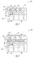
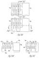
- FIGS. 1A-Dare illustrations of an embodiment of a structure of portions of a DRAM device 100 showing a MOS transistor 104 during various states of operation.
- DRAM device 100includes 1T capacitor-less memory cells each formed with one MOS transistor 104 .
- MOS transistor 104is formed on a base substrate 102 made of single crystalline silicon.
- a conductive bias gate layer 106is formed on a gate dielectric 105 over base substrate 102 .
- the bias gate layer 106is made of in situ doped (ISD) polysilicon.
- a floating body region 108is formed on a gate dielectric 107 over bias gate layer 106 and coupled between a source region 110 and a drain region 112 .
- Source region 110separates a source terminal 116 from floating body region 108 .
- Drain region 112separates a drain terminal 118 from floating body region 108 .
- a gate 114is formed on floating body region 108 between source region 110 and drain region 112 and is separated from source region 110 , drain region 112 , and floating body region 108 by a gate dielectric 115 .
- Gate 114is coupled between a gate terminal 120 from gate dielectric 115 .
- An oxide 122forms an isolation surrounding MOS transistor 104 .
- bias gate layer 106is formed after the formation of floating body region 108 .
- Bias gate layer 106is self-aligned to floating body region 108 as the conductive polysilicon is deposited onto base substrate 102 between the formed floating body regions 108 .
- base substrate 102 and floating body region 108are formed by a single crystalline silicon, and gate dielectrics 105 , 107 , and 115 include the same oxide formed at the same time during the fabrication process.
- An example of a process for fabricating MOS transistor 104is discussed below, with reference to FIGS. 7-15 . In FIGS. 2-3 and 9 - 15 , a gate dielectric exists between the gate and the source, drain, and floating body, between the bias gate and the floating body, and between the bias gate and the base substrate (though not explicitly shown or labeled).
- source terminal 116is coupled to a ground potential (0 V).
- Bias gate layer 106is coupled to a negative potential. In one embodiment, bias gate layer 106 is coupled to a negative potential between approximately ⁇ 0.25 V to ⁇ 2.0 V. In a specific embodiment, bias gate layer 106 is coupled to a negative potential of approximately ⁇ 1.0 V.
- FIG. 1Aillustrates an embodiment of the operation for writing logic “1”.
- gate terminal 120is coupled to a negative gate potential for writing
- drain terminal 118is coupled to a positive drain potential for writing.
- the negative gate potential and positive drain potentialcreate a gate-induced drain leakage (GIDL) current.
- Majority carriers (holes) 124are attracted to the negative potential of bias gate layer 106 , such that logic “1” is written into MOS transistor 104 .
- the negative gate potential for writingis between approximately ⁇ 1.5 V to ⁇ 3.0 V
- the positive drain potential for writingis between approximately 0.8 V to 2.0 V.
- the negative gate potential for writingis approximately ⁇ 2.5 V
- the positive drain potential for writingis approximately 1.8 V.
- gate terminal 120is coupled to a positive gate potential for writing
- drain terminal 118is coupled to a positive drain potential for writing.
- a lower positive gate potential and a higher positive drain potentialcreates impact ionization.
- MOS transistor 104operates in the current saturation region, causing a current to flow while allowing impact ionization to occur near drain region 112 .
- the impact ionizationproduces holes, which are attracted to the negative potential of bias gate layer 106 .
- the positive gate potential for writingis between approximately 0.7 V to 1.5 V
- the positive drain potential for writingis between approximately 1.0 V to 2.5 V.
- the positive gate potential for writingis approximately 1.0 V
- the positive drain potential for writingis approximately 1.5 V.
- FIG. 1Billustrates an embodiment of the operation for writing logic “0”, i.e., erasing logic “1”.
- gate terminal 120is coupled to a positive gate potential for erasing
- drain terminal 118is coupled to a negative drain potential for erasing.
- the inverted channel and the negative drain potentialcreate a potential that removes holes 124 from the region of floating body region 108 near bias gate layer 106 .
- the positive gate potential for erasingis between approximately 0.7 V to 1.5 V
- the negative drain potential for erasingis between approximately ⁇ 0.3 V to ⁇ 1.0 V.
- the positive gate potential for erasingis approximately 1.0 V
- the negative drain potential for erasingis approximately ⁇ 1.0 V.
- gate terminal 120is coupled to a negative gate potential for erasing
- drain terminal 118is coupled to a positive drain potential for erasing.
- the negative gate potential for erasingis between approximately ⁇ 1.5 V to ⁇ 3.0 V
- the positive drain potential for erasingis between approximately 0.0 V to 0.5 V.
- the negative gate potential for erasingis approximately ⁇ 1.8 V
- the positive drain potential for erasingis approximately 0.0 V (ground potential).
- the use of GIDL currentis limited to refresh or read-modify-write operations because the terminal potentials given above may not overwrite logic “1” with a logic “0”.
- the gate potentials for writing logic “1” and logic “0”are substantially the same. Because random data consisting of logic “1's” and “0's” are expected to be written, using the same gate potential avoids limiting the speed of operation due to the time required for changing the gate potential.
- FIG. 1Cillustrates an embodiment of the operation of reading.
- gate terminal 120is coupled to a positive gate potential for reading
- drain terminal 118is connected to a positive drain potential for reading.
- a high gate currentresults in a logic “1” reading.
- a low gate currentresults in a logic “0” reading.
- the positive gate potential for readingis between approximately 0.5 V to 1.5 V
- the positive drain potential for readingis between approximately 0.2 V to 1.0 V.
- the positive gate potential for readingis approximately 1.0 V
- the positive drain potential for readingis approximately 0.3 V.
- FIG. 1Dillustrates an embodiment of the operation of reading.
- gate terminal 120is coupled to a negative gate potential for holding, and drain terminal 118 is coupled to a positive drain potential.
- the negative gate potential for holdingis between approximately ⁇ 0.2 V to ⁇ 1.0 V
- the positive drain potential for readingis between approximately 0.0 V to 0.5 V.
- the negative gate potential for readingis approximately ⁇ 0.5 V
- the positive drain potential for readingis approximately 0 V (the ground potential).
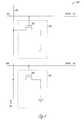
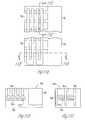
- FIG. 2is an illustration of an embodiment of the structure of portions of a DRAM device 200 , which represents a specific embodiment of DRAM device 100 .
- DRAM device 200includes 1T capacitor-less memory cells each formed with a MOS transistor 204 .
- MOS transistor 204is a specific embodiment of MOS transistor 104 and is implemented as a buried recessed-access device (RAD).
- RADburied recessed-access device
- MOS transistor 204is formed on base substrate 102 between oxide isolations 122 .
- MOS transistor 204includes bias gate layer 106 formed on base substrate 102 , floating body region 108 on bias gate layer 106 between source region 110 and drain region 112 , and buried gate dielectric 214 between source region 110 and drain region 112 .
- Source terminal 116is connected to a ground potential line 230 .
- Gate terminal 120is connected to a word line 232 .
- Drain terminal 118is connected to a bit line 234 via contact plug 236 .
- FIG. 3is an illustration of an embodiment of the structure of portions of a DRAM device 300 , which represents a specific embodiment of DRAM device 100 .
- DRAM device 300includes 1T capacitor-less memory cells each formed with a MOS transistor 304 .
- MOS transistor 304is a specific embodiment of MOS transistor 104 and is implemented as a strapped RAD.
- MOS transistor 304is formed on base substrate 102 between oxide isolations 122 .
- MOS transistor 304includes bias gate layer 106 formed on base substrate 102 , floating body region 108 on bias gate layer 106 between source region 110 and drain region 112 , and buried gate dielectric 314 between source region 110 and drain region 112 .
- Source terminal 116is connected to a ground potential line 330 via contact plug 336 .
- Gate terminal 118is connected to a word line 332 .
- Drain terminalis connected to a bit line 334 .
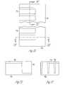
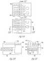
- FIG. 4is a circuit schematic illustrating a portion of a DRAM device 400 including DRAM cells 410 .
- DRAM cells 410are 1T capacitor-less memory cells each include a MOS transistor 404 .
- MOS transistor 404is MOS transistor 104 .
- MOS transistor 404is MOS transistor 204 or MOS transistor 304 .
- MOS transistor 404has a drain terminal coupled to a bit line 406 , a gate terminal coupled to a word line 408 , and a source terminal coupled to a ground potential.
- FIG. 5is a block diagram illustrating an embodiment of a memory device 520 utilizing MOS transistor 104 (including its specific embodiments such as MOS transistors 204 or 304 ).
- Memory device 520contains a memory array 522 , a row decoder 524 , a column decoder 528 , and sense amplifiers 526 .
- Memory array 522includes a plurality of transistor cells 540 each being a 1T capacitor-less memory cell formed with a MOS transistor such as MOS transistor 104 .
- Word lines 538 and bit lines 530are commonly arranged into rows and columns. Bit lines 530 of memory array 522 are connected to sense amplifiers 526 , while word lines 538 are connected to row decoder 524 .
- Address and control signalsare input on address/control lines 532 into memory device 520 and are connected to column decoder 528 , sense amplifiers 526 , and row decoder 524 , and are used to gain read and write access, among other things, to memory array 522 .
- Column decoder 528is connected to sense amplifiers 526 via control and column select signals on column select lines 534 .
- Sense amplifiers 526receives input data destined for memory array 522 , and outputs data read from memory array 522 over input/output (I/O) data lines 536 .
- Datais read from the cells of memory array 522 by activating one of the word lines 538 (via the row decoder 524 ), which couples all of the memory cells corresponding to that word line to respective bit lines 530 , which define the columns of the array.
- One or more bit lines 530are also activated.
- sense amplifiers 526When a particular word line 538 and bit lines 530 are activated, sense amplifiers 526 connected to a bit line column detects and amplifies the conduction sensed through a given transistor cell and transferred to its bit line 530 by measuring the potential difference between the activated bit line 530 and a reference line which may be an inactive bit line. In the read operation the source region of a given cell is coupled to bit line.
- the operation of Memory device sense amplifiersis described, for example, in U.S. Pat. Nos. 5,627,785; 5,280,205; and 5,042,011, all assigned to Micron Technology Inc., the specification of which are incorporated by reference herein in their entirety.
- FIG. 6is a block diagram illustrating an embodiment of a processor-based system utilizing MOS transistor 104 (including its specific embodiments such as MOS transistors 204 or 304 ).
- FIG. 6is a block diagram of an electrical system, or processor-based system, 600 utilizing 1T capacitor-less memory cells each formed with a MOS transistor such as MOS transistor 104 .
- the processor-based system 600may be a computer system, a process control system or any other system employing a processor and associated memory.
- System 600includes a central processing unit (CPU) 652 , e.g., a microprocessor that communicates with the memory 662 and an I/O device 658 over a bus 690 .
- CPUcentral processing unit
- bus 690may be a series of buses and bridges commonly used in a processor-based system, but for convenience purposes only, bus 690 has been illustrated as a single bus.
- a second I/O device 660is illustrated, but is not necessary.
- the processor-based system 600can also include read-only memory (ROM) 664 and may include peripheral devices such as a floppy disk drive 654 and a compact disk (CD) ROM drive 656 that also communicates with the CPU 652 over the bus 690 as is well known in the art.
- ROMread-only memory
- CDcompact disk
- FIG. 6illustrates an embodiment for electronic system circuitry in which one or more transistors including those as illustrated in FIGS. 1A-D , 2 , and 3 are used.
- the illustration of system 600is intended to provide a general understanding of one application for the structure and circuitry of the present invention, and is not intended to serve as a complete description of all the elements and features of an electronic system using the novel 1T capacitor-less memory cells discussed in this document. Further, the invention is equally applicable to any size and type of system 600 using the one or more transistors including those as illustrated in FIGS. 1A-D , 2 , and 3 , and is not intended to be limited to that described above. As one of ordinary skill in the art will understand, such an electronic system can be fabricated in single-package processing units, or even on a single semiconductor chip, in order to reduce the communication time between the processor and the memory device.
- MOS transistor 104Applications containing MOS transistors each having a floating body region separated from a base substrate by a conductive biased gate layer, such as MOS transistor 104 and its specific embodiments described in this document, include electronic systems for use in memory modules, device drivers, power modules, communication modems, processor modules, and application-specific modules, and may include multilayer, multichip modules.
- Such circuitrycan further be a subcomponent of a variety of electronic systems, such as a clock, a television, a cell phone, a personal computer, an automobile, an industrial control system, an aircraft, and others.
- FIGS. 7-15illustrate an embodiment of a fabrication process for a DRAM device according to the present subject matter.
- FIGS. 7-15 and the associated description belowillustrate the process of making MOS transistors having floating body regions separated from a base substrate by a bias gate layer, such as MOS transistors 104 , 204 , and 304 as discussed above. While not intended to be a full description of the fabrication process, FIGS. 7-15 and the associated description below provide sufficient details to enable those skilled in the art to make 1T capacitor-less memory devices by practicing the invention.
- the size of each physical structure of a memory deviceis described by the size of electrically conductive lines (word and bit lines) in terms of lithographic feature size (F).
- the lithographic feature size (F)is one half of the minimum pitch, i.e., one half of the sum of the width of one of the electrically conductive lines and the width of the isolation space between the electrically conductive lines.
- An 8F 2 memory cellrefers to a memory cell that has an area of 8 square lithographic features. Specific sizes discussed below with references to FIGS. 7-15 are based on a process for fabricating of 8F 2 memory cells. However, the process illustrated in FIGS. 7-15 is generally applicable to fabricate memory cells with other cell sizes.
- FIGS. 7A-Cillustrate the formation of shallow-trench-isolations (STIs) 702 and active areas between the STIs 702 .
- FIG. 7Ais a top view of the DRAM device being fabricated, and FIGS. 7B-C are each a cross-sectional view.
- Shallow-trench-isolations 702 and the active areasare formed on a silicon base substrate 700 .
- the active areasare each 3F wide.
- STIs 702are each 1F wide and made of silicon oxide (SiO 2 ).
- the depth of each STI 702is about 3,500 angstroms ( ⁇ ).
- a nitride cap 704is formed on each active area.
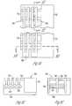
- FIGS. 8A-Cillustrate the formation of silicon islands 810 .
- FIG. 8Ais a top view of the DRAM device being fabricated, and FIGS. 8B-C are each a cross-sectional view.
- Silicon islands 810are formed using a pattern of 1F lines separated by 1F spaces and perpendicular to the STIs 702 and the active areas.
- An in situ trench etchis performed to remove both STIs 702 and the active areas along the 1F lines with a depth of about 2,000 angstroms.
- An in situ undercut etchis then performed to form the silicon islands 810 by disconnecting them from base substrate 700 .
- Silicon islands 810are held by STIs 702 .
- Nitride cap 704also helps prevent silicon islands 810 from being broken off.
- FIGS. 9A-Cillustrate the formation of a conductive bias gate layer 920 .
- FIG. 9Ais a top view of the DRAM device being fabricated, and FIGS. 9B-C are each a cross-sectional view.
- nitride cap 704intact, the exposed silicon is oxidized to form gate dielectric.
- In situ-doped (ISD) polysiliconis deposited to fill the gaps between silicon islands 810 .
- a combination of chemical-mechanical polishing (CMP) and reactive ion etching (RIE), or a simple RIE,is performed to recess the ISD polysilicon at about 1,500 angstroms from a surface 924 , which is the top surface of the device during the fabrication process.
- CMPchemical-mechanical polishing
- RIEreactive ion etching
- bias gate layer 920is defined and self-aligned to silicon islands 810 .
- Voids 922may be present in the ISD polysilicon, which do not affect the function of bias gate layer 920 .
- Bias gate layer 920separates silicon islands 810 from base substrate 700 .
- the gate dielectric formed on the exposed silicon before the deposition of the ISD polysiliconinsulates silicon islands 810 , thus making silicon islands 810 the floating bodies of MOS transistors. That is, when the fabrication process for the DRAM device is completed, each silicon island becomes floating body region 108 , and each bias gate 920 becomes bias gate layer 106 , of a MOS transistor such as MOS transistor 104 , 204 , or 304 as discussed above.
- FIGS. 10A-Cillustrate planarization of surface 924 .
- FIG. 10Ais a top view of the DRAM device being fabricated, and FIGS. 10B-C are each a cross-sectional view.
- the exposed ISD polysilicon of bias gate layer 920is oxidized using thin oxidation.
- the trenchesare filled with SiO 2 , such as by nitride liner and spin-on-dielectric (SID).
- SIDspin-on-dielectric
- a stop-on-nitride (SON) CMPis then performed.
- Surface 924is thus planarized, with sacrificial nitride exposed for subsequent wet nitride removal.
- FIGS. 11A-Cillustrate removal of nitride cap 704 .
- FIG. 11Ais a top view of the DRAM device being fabricated, and FIGS. 11B-C are each a cross-sectional view.
- the remaining portions of nitride cap 704are removed by a hot phosphoric wet nitride removal.
- Thick or thin gate dielectricis formed by oxidation.
- FIGS. 12A-Cillustrate the formation of array recessed gates 1230 .
- FIG. 12Ais a top view of the DRAM device being fabricated, and FIGS. 12B-C are each a cross-sectional view.
- recessed-access-deviceRAD
- Silicon islands 810are recessed by trench etch to about 1,000 angstroms below surface 924 .
- the resultant exposed siliconis oxidized to form the gate dielectric.
- Array and “dummy” gatesmay be defined at the same time.
- Dummy (ground) gates 1232are defined in the array over STIs 702 to isolate the subsequent polysilicon plugs.
- Gate nitride spacers 1234are formed on array recessed gates 1230 and dummy gates 1232 .
- FIGS. 13A-Cillustrate the formation of drain and source polysilicon plugs 1340 .
- FIG. 13Ais a top view of the DRAM device being fabricated, and FIGS. 13B-C are each a cross-sectional view.
- Drain and source implantmay be done before or after the formation of gate nitride spacers 1234 to enhance the GIDL effects.
- Drain and source polysilicon plugs 1340are formed by teos or phosphor-silicon-glass or boro-phosphor-silicon-glass deposition and reflow.
- a stop-on-nitride (SON) CMPfollows. In one embodiment, adjacent source contacts are arranged to tie together to lower contact resistance.
- FIGS. 14A-Cillustrate the formation of common source interconnections 1450 .
- FIG. 14Ais a top view of the DRAM device being fabricated, and FIGS. 14B-C are each a cross-sectional view.
- a thin oxideis deposited on surface 924 , followed by a common source contact etch to open the source contact.
- a common source interconnect conductor 1452is deposited.
- a nitride cap 1454is formed on the common source interconnect conductor 1452 .
- FIGS. 15A-Cillustrate the formation of array drain and peripheral local interconnections.
- FIG. 15Ais a top view of the DRAM device being fabricated, and FIGS. 15B-C are each a cross-sectional view.
- Drain interconnects (bit lines) 1560are each formed with an interconnect conductor 1562 , and nitride cap 1564 is deposited on the interconnect conductor 1562 .
- the interconnect conductorinclude TiSix/W and metal-mode-titanium/Tungsten (MMTi/W).
- MMTi/Wmetal-mode-titanium/Tungsten
- An example of the material forming the nitride capis Si 3 N 4 .
- Array drain contactsare self-aligned-contact (SAC) etched to expose the polysilicon below. Peripheral contacts of the interconnects are exposed by etching.
- the peripheral contacts illustrated in FIG. 15Ainclude source contacts 1570 , gate contacts 1572 , drain contacts 1574 , and bias gate contacts 1756 . These contacts are each connected to a potential line that is to be coupled to a specified potential during the operation of the DRAM device.
- the specified potentialmay be constant during the operation, such as the potential coupled to the source terminal and the bias gate layer of a MOS transistor of the DRAM device, or variable during the operation, such as the potential coupled to the gate terminal and the drain terminal of the MOS transistor.
- An example of the potentials to which source contacts 1570 , gate contacts 1572 , drain contacts 1574 , and bias gate contacts 1756 are coupled to during the operation of the DRAM deviceis given above in FIGS. 1A-D and the associated discussion.
- source contact 1570is coupled to source terminal 116
- gate contact 1572is coupled to gate terminal 120
- drain contact 1574is coupled to drain terminal 118
- bias gate contact 1756is coupled to bias gate layer 106 .
Landscapes
- Engineering & Computer Science (AREA)
- Manufacturing & Machinery (AREA)
- Microelectronics & Electronic Packaging (AREA)
- Computer Hardware Design (AREA)
- Semiconductor Memories (AREA)
Abstract
Description
Claims (15)
Priority Applications (2)
| Application Number | Priority Date | Filing Date | Title |
|---|---|---|---|
| US12/537,470US7944743B2 (en) | 2006-09-07 | 2009-08-07 | Methods of making a semiconductor memory device |
| US13/071,979US8446762B2 (en) | 2006-09-07 | 2011-03-25 | Methods of making a semiconductor memory device |
Applications Claiming Priority (2)
| Application Number | Priority Date | Filing Date | Title |
|---|---|---|---|
| US11/516,814US7589995B2 (en) | 2006-09-07 | 2006-09-07 | One-transistor memory cell with bias gate |
| US12/537,470US7944743B2 (en) | 2006-09-07 | 2009-08-07 | Methods of making a semiconductor memory device |
Related Parent Applications (1)
| Application Number | Title | Priority Date | Filing Date |
|---|---|---|---|
| US11/516,814DivisionUS7589995B2 (en) | 2006-09-07 | 2006-09-07 | One-transistor memory cell with bias gate |
Related Child Applications (1)
| Application Number | Title | Priority Date | Filing Date |
|---|---|---|---|
| US13/071,979ContinuationUS8446762B2 (en) | 2006-09-07 | 2011-03-25 | Methods of making a semiconductor memory device |
Publications (2)
| Publication Number | Publication Date |
|---|---|
| US20090311845A1 US20090311845A1 (en) | 2009-12-17 |
| US7944743B2true US7944743B2 (en) | 2011-05-17 |
Family
ID=38981012
Family Applications (3)
| Application Number | Title | Priority Date | Filing Date |
|---|---|---|---|
| US11/516,814Active2027-03-07US7589995B2 (en) | 2006-09-07 | 2006-09-07 | One-transistor memory cell with bias gate |
| US12/537,470ActiveUS7944743B2 (en) | 2006-09-07 | 2009-08-07 | Methods of making a semiconductor memory device |
| US13/071,979ActiveUS8446762B2 (en) | 2006-09-07 | 2011-03-25 | Methods of making a semiconductor memory device |
Family Applications Before (1)
| Application Number | Title | Priority Date | Filing Date |
|---|---|---|---|
| US11/516,814Active2027-03-07US7589995B2 (en) | 2006-09-07 | 2006-09-07 | One-transistor memory cell with bias gate |
Family Applications After (1)
| Application Number | Title | Priority Date | Filing Date |
|---|---|---|---|
| US13/071,979ActiveUS8446762B2 (en) | 2006-09-07 | 2011-03-25 | Methods of making a semiconductor memory device |
Country Status (4)
| Country | Link |
|---|---|
| US (3) | US7589995B2 (en) |
| KR (1) | KR101057204B1 (en) |
| TW (1) | TWI353041B (en) |
| WO (1) | WO2008030588A1 (en) |
Cited By (4)
| Publication number | Priority date | Publication date | Assignee | Title |
|---|---|---|---|---|
| US20120168879A1 (en)* | 2010-12-29 | 2012-07-05 | Semiconductor Manufacturing International (Beijing) Corporation | Transistor and method for forming the same |
| US8446762B2 (en)* | 2006-09-07 | 2013-05-21 | Micron Technology, Inc. | Methods of making a semiconductor memory device |
| US10515801B2 (en) | 2007-06-04 | 2019-12-24 | Micron Technology, Inc. | Pitch multiplication using self-assembling materials |
| US10644003B2 (en) | 2016-12-02 | 2020-05-05 | Samsung Electronics Co., Ltd. | Semiconductor memory devices having bit line node contact between bit line and active region |
Families Citing this family (48)
| Publication number | Priority date | Publication date | Assignee | Title |
|---|---|---|---|---|
| US7547945B2 (en) | 2004-09-01 | 2009-06-16 | Micron Technology, Inc. | Transistor devices, transistor structures and semiconductor constructions |
| US7518196B2 (en)* | 2005-02-23 | 2009-04-14 | Intel Corporation | Field effect transistor with narrow bandgap source and drain regions and method of fabrication |
| US7384849B2 (en) | 2005-03-25 | 2008-06-10 | Micron Technology, Inc. | Methods of forming recessed access devices associated with semiconductor constructions |
| US7282401B2 (en) | 2005-07-08 | 2007-10-16 | Micron Technology, Inc. | Method and apparatus for a self-aligned recessed access device (RAD) transistor gate |
| US7867851B2 (en) | 2005-08-30 | 2011-01-11 | Micron Technology, Inc. | Methods of forming field effect transistors on substrates |
| US7700441B2 (en) | 2006-02-02 | 2010-04-20 | Micron Technology, Inc. | Methods of forming field effect transistors, methods of forming field effect transistor gates, methods of forming integrated circuitry comprising a transistor gate array and circuitry peripheral to the gate array, and methods of forming integrated circuitry comprising a transistor gate array including first gates and second grounded isolation gates |
| US7602001B2 (en) | 2006-07-17 | 2009-10-13 | Micron Technology, Inc. | Capacitorless one transistor DRAM cell, integrated circuitry comprising an array of capacitorless one transistor DRAM cells, and method of forming lines of capacitorless one transistor DRAM cells |
| US7772632B2 (en) | 2006-08-21 | 2010-08-10 | Micron Technology, Inc. | Memory arrays and methods of fabricating memory arrays |
| US7858471B2 (en)* | 2006-09-13 | 2010-12-28 | Micron Technology, Inc. | Methods of fabricating an access transistor for an integrated circuit device, methods of fabricating periphery transistors and access transistors, and methods of fabricating an access device comprising access transistors in an access circuitry region and peripheral transistors in a peripheral circuitry region spaced from the access circuitry region |
| US7598560B2 (en) | 2007-03-30 | 2009-10-06 | Kavalieros Jack T | Hetero-bimos injection process for non-volatile flash memory |
| KR20090132872A (en)* | 2008-06-23 | 2009-12-31 | 삼성전자주식회사 | Semiconductor Devices and Semiconductor Substrates |
| US8067803B2 (en)* | 2008-10-16 | 2011-11-29 | Micron Technology, Inc. | Memory devices, transistor devices and related methods |
| US8278167B2 (en)* | 2008-12-18 | 2012-10-02 | Micron Technology, Inc. | Method and structure for integrating capacitor-less memory cell with logic |
| KR101528817B1 (en)* | 2009-01-09 | 2015-06-16 | 삼성전자주식회사 | Semiconductor memory device and method of manufacturing the same |
| KR101544509B1 (en)* | 2009-02-03 | 2015-08-13 | 삼성전자주식회사 | Method for manufacturing semiconductor device having transistor |
| KR101073643B1 (en)* | 2009-02-19 | 2011-10-14 | 서울대학교산학협력단 | High performance 1T-DRAM cell device and manufacturing method thereof |
| US8148780B2 (en) | 2009-03-24 | 2012-04-03 | Micron Technology, Inc. | Devices and systems relating to a memory cell having a floating body |
| US7929343B2 (en)* | 2009-04-07 | 2011-04-19 | Micron Technology, Inc. | Methods, devices, and systems relating to memory cells having a floating body |
| WO2010114406A1 (en)* | 2009-03-30 | 2010-10-07 | Murashev Viktor Nikolaevich | Memory cell for a high-speed eeprom and a method for programming same |
| US8508994B2 (en) | 2009-04-30 | 2013-08-13 | Micron Technology, Inc. | Semiconductor device with floating gate and electrically floating body |
| US8288795B2 (en)* | 2010-03-02 | 2012-10-16 | Micron Technology, Inc. | Thyristor based memory cells, devices and systems including the same and methods for forming the same |
| US8513722B2 (en) | 2010-03-02 | 2013-08-20 | Micron Technology, Inc. | Floating body cell structures, devices including same, and methods for forming same |
| US9608119B2 (en) | 2010-03-02 | 2017-03-28 | Micron Technology, Inc. | Semiconductor-metal-on-insulator structures, methods of forming such structures, and semiconductor devices including such structures |
| US8507966B2 (en)* | 2010-03-02 | 2013-08-13 | Micron Technology, Inc. | Semiconductor cells, arrays, devices and systems having a buried conductive line and methods for forming the same |
| US9646869B2 (en) | 2010-03-02 | 2017-05-09 | Micron Technology, Inc. | Semiconductor devices including a diode structure over a conductive strap and methods of forming such semiconductor devices |
| US8859367B2 (en) | 2010-07-09 | 2014-10-14 | Micron Technology, Inc. | Gate constructions of recessed access devices and methods of forming gate constructions of recessed access devices |
| US8598621B2 (en) | 2011-02-11 | 2013-12-03 | Micron Technology, Inc. | Memory cells, memory arrays, methods of forming memory cells, and methods of forming a shared doped semiconductor region of a vertically oriented thyristor and a vertically oriented access transistor |
| US8952418B2 (en) | 2011-03-01 | 2015-02-10 | Micron Technology, Inc. | Gated bipolar junction transistors |
| US8519431B2 (en) | 2011-03-08 | 2013-08-27 | Micron Technology, Inc. | Thyristors |
| US8648414B2 (en)* | 2011-07-01 | 2014-02-11 | Micron Technology, Inc. | Semiconductor structures including bodies of semiconductor material, devices including such structures and related methods |
| US8772848B2 (en) | 2011-07-26 | 2014-07-08 | Micron Technology, Inc. | Circuit structures, memory circuitry, and methods |
| KR20130017647A (en)* | 2011-08-11 | 2013-02-20 | 삼성전자주식회사 | Method of fabricating resistance variable memory device |
| US9472542B2 (en)* | 2013-09-11 | 2016-10-18 | Micron Technology, Inc. | DRAM arrays, semiconductor constructions and DRAM array layouts |
| US9263357B2 (en) | 2013-12-06 | 2016-02-16 | Infineon Technologies Dresden Gmbh | Carrier with hollow chamber and support structure therein |
| US9560765B2 (en)* | 2013-12-06 | 2017-01-31 | Infineon Technologies Dresden Gmbh | Electronic device, a method for manufacturing an electronic device, and a method for operating an electronic device |
| US9613878B2 (en) | 2013-12-06 | 2017-04-04 | Infineon Technologies Dresden Gmbh | Carrier and a method for processing a carrier |
| KR102293245B1 (en) | 2015-03-27 | 2021-08-26 | 에스케이하이닉스 주식회사 | Semiconductor device and method for manufacturing the same |
| US10833175B2 (en)* | 2015-06-04 | 2020-11-10 | International Business Machines Corporation | Formation of dislocation-free SiGe finFET using porous silicon |
| CN105514121B (en)* | 2016-01-26 | 2019-03-15 | 武汉华星光电技术有限公司 | A TFT array substrate and its manufacturing method |
| CN106960683B (en)* | 2017-03-31 | 2020-05-05 | 深圳市华星光电技术有限公司 | Dynamic random access memory applied to liquid crystal display and access method thereof |
| US11367734B2 (en)* | 2020-02-04 | 2022-06-21 | Globalfoundries U.S. Inc. | Charge trap memory devices |
| CN111354797B (en)* | 2020-03-12 | 2023-03-10 | 上海华虹宏力半导体制造有限公司 | Radio frequency device and method of forming the same |
| WO2022269735A1 (en)* | 2021-06-22 | 2022-12-29 | ユニサンティス エレクトロニクス シンガポール プライベート リミテッド | Memory device using semiconductor element |
| US12293913B1 (en)* | 2021-12-22 | 2025-05-06 | Intel Corporation | Directed self-assembly enabled subtractive metal patterning |
| KR20230140036A (en) | 2022-03-29 | 2023-10-06 | 삼성전자주식회사 | Body bias voltage generator and semiconductor device including the same |
| EP4394772A4 (en) | 2022-04-02 | 2025-08-27 | Beijing Superstring Academy Of Memory Tech | MEMORY AND MANUFACTURING METHOD THEREFOR, AND ELECTRONIC DEVICE |
| CN114863970B (en)* | 2022-04-02 | 2023-02-17 | 北京超弦存储器研究院 | Dynamic memory, manufacturing method thereof, reading method thereof and storage device |
| TWI845415B (en)* | 2022-10-24 | 2024-06-11 | 國立中央大學 | Memory circuit, dynamic random access memory and operation method thereof |
Citations (190)
| Publication number | Priority date | Publication date | Assignee | Title |
|---|---|---|---|---|
| US4455740A (en) | 1979-12-07 | 1984-06-26 | Tokyo Shibaura Denki Kabushiki Kaisha | Method of manufacturing a self-aligned U-MOS semiconductor device |
| US4835741A (en) | 1986-06-02 | 1989-05-30 | Texas Instruments Incorporated | Frasable electrically programmable read only memory cell using a three dimensional trench floating gate |
| US4922460A (en) | 1987-01-26 | 1990-05-01 | Mitsubishi Denki Kabushiki Kaisha | Semiconductor memory device with folded bit line structure suitable for high density |
| US4931409A (en) | 1988-01-30 | 1990-06-05 | Kabushiki Kaisha Toshiba | Method of manufacturing semiconductor device having trench isolation |
| US4937641A (en) | 1983-09-28 | 1990-06-26 | Hitachi, Ltd. | Semiconductor memory and method of producing the same |
| US4979004A (en) | 1988-01-29 | 1990-12-18 | Texas Instruments Incorporated | Floating gate memory cell and device |
| US5013680A (en) | 1990-07-18 | 1991-05-07 | Micron Technology, Inc. | Process for fabricating a DRAM array having feature widths that transcend the resolution limit of available photolithography |
| US5014110A (en) | 1988-06-03 | 1991-05-07 | Mitsubishi Denki Kabushiki Kaisha | Wiring structures for semiconductor memory device |
| US5021355A (en) | 1989-05-22 | 1991-06-04 | International Business Machines Corporation | Method of fabricating cross-point lightly-doped drain-source trench transistor |
| US5047117A (en) | 1990-09-26 | 1991-09-10 | Micron Technology, Inc. | Method of forming a narrow self-aligned, annular opening in a masking layer |
| US5107459A (en) | 1990-04-20 | 1992-04-21 | International Business Machines Corporation | Stacked bit-line architecture for high density cross-point memory cell array |
| US5108938A (en) | 1989-03-21 | 1992-04-28 | Grumman Aerospace Corporation | Method of making a trench gate complimentary metal oxide semiconductor transistor |
| US5122848A (en) | 1991-04-08 | 1992-06-16 | Micron Technology, Inc. | Insulated-gate vertical field-effect transistor with high current drive and minimum overlap capacitance |
| US5160491A (en) | 1986-10-21 | 1992-11-03 | Texas Instruments Incorporated | Method of making a vertical MOS transistor |
| US5254218A (en) | 1992-04-22 | 1993-10-19 | Micron Technology, Inc. | Masking layer having narrow isolated spacings and the method for forming said masking layer and the method for forming narrow isolated trenches defined by said masking layer |
| US5281548A (en) | 1992-07-28 | 1994-01-25 | Micron Technology, Inc. | Plug-based floating gate memory |
| US5358879A (en) | 1993-04-30 | 1994-10-25 | Loral Federal Systems Company | Method of making gate overlapped lightly doped drain for buried channel devices |
| US5371024A (en) | 1988-09-30 | 1994-12-06 | Kabushiki Kaisha Toshiba | Semiconductor device and process for manufacturing the same |
| US5376575A (en) | 1991-09-26 | 1994-12-27 | Hyundai Electronics Industries, Inc. | Method of making dynamic random access memory having a vertical transistor |
| US5392237A (en) | 1992-09-25 | 1995-02-21 | Rohm Co., Ltd. | Semiconductor memory device with EEPROM in trench with polysilicon/metal contacting to source and drain in virtual ground type array |
| US5413949A (en) | 1994-04-26 | 1995-05-09 | United Microelectronics Corporation | Method of making self-aligned MOSFET |
| US5446299A (en) | 1994-04-29 | 1995-08-29 | International Business Machines Corporation | Semiconductor random access memory cell on silicon-on-insulator with dual control gates |
| US5480838A (en) | 1992-07-03 | 1996-01-02 | Mitsubishi Denki Kabushiki Kaisha | Method of manufacturing a semiconductor device having vertical transistor with tubular double-gate |
| US5502320A (en) | 1993-03-15 | 1996-03-26 | Kabushiki Kaisha Toshiba | Dynamic random access memory (DRAM) semiconductor device |
| US5514604A (en) | 1993-12-08 | 1996-05-07 | General Electric Company | Vertical channel silicon carbide metal-oxide-semiconductor field effect transistor with self-aligned gate for microwave and power applications, and method of making |
| US5574621A (en) | 1995-03-27 | 1996-11-12 | Motorola, Inc. | Integrated circuit capacitor having a conductive trench |
| US5573837A (en) | 1992-04-22 | 1996-11-12 | Micron Technology, Inc. | Masking layer having narrow isolated spacings and the method for forming said masking layer and the method for forming narrow isolated trenches defined by said masking layer |
| US5612559A (en) | 1993-11-24 | 1997-03-18 | Samsung Electronics Co., Ltd. | Semiconductor device having pillar shaped transistor and a method for manufacturing the same |
| US5619057A (en) | 1994-01-19 | 1997-04-08 | Sony Corporation | Complex film overlying a substrate with defined work function |
| EP0453998B1 (en) | 1990-04-21 | 1997-07-02 | Kabushiki Kaisha Toshiba | Semiconductor memory device having a bit line constituted by a semiconductor layer |
| US5693549A (en) | 1994-09-13 | 1997-12-02 | Lg Semicon Co., Ltd. | Method of fabricating thin film transistor with supplementary gates |
| US5714786A (en) | 1996-10-31 | 1998-02-03 | Micron Technology, Inc. | Transistors having controlled conductive spacers, uses of such transistors and methods of making such transistors |
| US5714412A (en) | 1996-12-02 | 1998-02-03 | Taiwan Semiconductor Manufacturing Company, Ltd | Multi-level, split-gate, flash memory cell and method of manufacture thereof |
| US5739066A (en) | 1996-09-17 | 1998-04-14 | Micron Technology, Inc. | Semiconductor processing methods of forming a conductive gate and line |
| US5753947A (en) | 1995-01-20 | 1998-05-19 | Micron Technology, Inc. | Very high-density DRAM cell structure and method for fabricating it |
| US5763305A (en) | 1996-08-16 | 1998-06-09 | United Microelectronics Corporation | Method for forming a semiconductor memory device with a capacitor |
| US5792690A (en) | 1997-05-15 | 1998-08-11 | Vanguard International Semiconductor Corporation | Method of fabricating a DRAM cell with an area equal to four times the used minimum feature |
| US5792687A (en) | 1996-08-01 | 1998-08-11 | Vanguard International Semiconductor Corporation | Method for fabricating high density integrated circuits using oxide and polysilicon spacers |
| US5798544A (en) | 1994-04-22 | 1998-08-25 | Nec Corporation | Semiconductor memory device having trench isolation regions and bit lines formed thereover |
| US5817552A (en) | 1995-05-24 | 1998-10-06 | Siemens Aktiengesellschaft | Process of making a dram cell arrangement |
| US5841611A (en) | 1994-05-02 | 1998-11-24 | Matsushita Electric Industrial Co., Ltd. | Magnetoresistance effect device and magnetoresistance effect type head, memory device, and amplifying device using the same |
| US5869359A (en) | 1997-08-20 | 1999-02-09 | Prabhakar; Venkatraman | Process for forming silicon on insulator devices having elevated source and drain regions |
| US5909618A (en) | 1997-07-08 | 1999-06-01 | Micron Technology, Inc. | Method of making memory cell with vertical transistor and buried word and body lines |
| US5963469A (en) | 1998-02-24 | 1999-10-05 | Micron Technology, Inc. | Vertical bipolar read access for low voltage memory cell |
| US5972754A (en) | 1998-06-10 | 1999-10-26 | Mosel Vitelic, Inc. | Method for fabricating MOSFET having increased effective gate length |
| US5977579A (en) | 1998-12-03 | 1999-11-02 | Micron Technology, Inc. | Trench dram cell with vertical device and buried word lines |
| US6015990A (en) | 1997-02-27 | 2000-01-18 | Kabushiki Kaisha Toshiba | Semiconductor memory device and method of manufacturing the same |
| US6033963A (en) | 1999-08-30 | 2000-03-07 | Taiwan Semiconductor Manufacturing Company | Method of forming a metal gate for CMOS devices using a replacement gate process |
| US6054355A (en) | 1997-06-30 | 2000-04-25 | Kabushiki Kaisha Toshiba | Method of manufacturing a semiconductor device which includes forming a dummy gate |
| EP1003219A2 (en) | 1998-11-19 | 2000-05-24 | Siemens Aktiengesellschaft | DRAM with stacked capacitor and buried word line |
| US6072209A (en) | 1997-07-08 | 2000-06-06 | Micro Technology, Inc. | Four F2 folded bit line DRAM cell structure having buried bit and word lines |
| DE19928781C1 (en) | 1999-06-23 | 2000-07-06 | Siemens Ag | DRAM cell array has deep word line trenches for increasing transistor channel length and has no fixed potential word lines separating adjacent memory cells |
| US6114735A (en) | 1999-07-02 | 2000-09-05 | Micron Technology, Inc. | Field effect transistors and method of forming field effect transistors |
| US6124611A (en) | 1998-10-30 | 2000-09-26 | Sony Corporation | Epitaxial channel vertical MOS transistor |
| US6150687A (en) | 1997-07-08 | 2000-11-21 | Micron Technology, Inc. | Memory cell having a vertical transistor with buried source/drain and dual gates |
| US6168996B1 (en) | 1997-08-28 | 2001-01-02 | Hitachi, Ltd. | Method of fabricating semiconductor device |
| US6184086B1 (en) | 1995-11-20 | 2001-02-06 | Micron Technology Inc. | Method for forming a floating gate semiconductor device having a portion within a recess |
| US6187643B1 (en) | 1999-06-29 | 2001-02-13 | Varian Semiconductor Equipment Associates, Inc. | Simplified semiconductor device manufacturing using low energy high tilt angle and high energy post-gate ion implantation (PoGI) |
| US6191470B1 (en) | 1997-07-08 | 2001-02-20 | Micron Technology, Inc. | Semiconductor-on-insulator memory cell with buried word and body lines |
| US6215149B1 (en) | 1998-08-18 | 2001-04-10 | Samsung Electronics Co., Ltd. | Trenched gate semiconductor device |
| US6225669B1 (en) | 1998-09-30 | 2001-05-01 | Advanced Micro Devices, Inc. | Non-uniform gate/dielectric field effect transistor |
| US6255165B1 (en) | 1999-10-18 | 2001-07-03 | Advanced Micro Devices, Inc. | Nitride plug to reduce gate edge lifting |
| US6259142B1 (en) | 1998-04-07 | 2001-07-10 | Advanced Micro Devices, Inc. | Multiple split gate semiconductor device and fabrication method |
| US6297106B1 (en) | 1999-05-07 | 2001-10-02 | Chartered Semiconductor Manufacturing Ltd. | Transistors with low overlap capacitance |
| US20010025973A1 (en) | 2000-01-25 | 2001-10-04 | Satoru Yamada | Semiconductor integrated circuit device and process for manufacturing the same |
| US6300177B1 (en) | 2001-01-25 | 2001-10-09 | Chartered Semiconductor Manufacturing Inc. | Method to form transistors with multiple threshold voltages (VT) using a combination of different work function gate materials |
| US6301726B1 (en) | 2000-11-27 | 2001-10-16 | Robert Pena | Method of installing a bathtub |
| US20010038123A1 (en) | 1999-08-11 | 2001-11-08 | Bin Yu | Transistor with dynamic source/drain extensions |
| US6323506B1 (en) | 1999-12-21 | 2001-11-27 | Philips Electronics North America Corporation | Self-aligned silicon carbide LMOSFET |
| US20010052617A1 (en) | 2000-03-01 | 2001-12-20 | Shindengen Electric Manufacturing Co., Ltd | Transistor and method of manufacturing the same |
| US6337497B1 (en) | 1997-05-16 | 2002-01-08 | International Business Machines Corporation | Common source transistor capacitor stack |
| US6340614B1 (en) | 2000-10-03 | 2002-01-22 | Vanguard International Semiconductor Corporation | Method of forming a DRAM cell |
| US6348385B1 (en) | 2000-11-30 | 2002-02-19 | Chartered Semiconductor Manufacturing Ltd. | Method for a short channel CMOS transistor with small overlay capacitance using in-situ doped spacers with a low dielectric constant |
| US6349052B1 (en) | 1999-09-13 | 2002-02-19 | Infineon Technologies Ag | DRAM cell arrangement and method for fabricating it |
| US6362506B1 (en) | 1998-08-26 | 2002-03-26 | Texas Instruments Incorporated | Minimization-feasible word line structure for DRAM cell |
| US6383879B1 (en) | 1999-12-03 | 2002-05-07 | Agere Systems Guardian Corp. | Semiconductor device having a metal gate with a work function compatible with a semiconductor device |
| US6391726B1 (en) | 1999-03-11 | 2002-05-21 | Micron Technology, Inc. | Method of fabricating integrated circuitry |
| US6414356B1 (en) | 1998-03-30 | 2002-07-02 | Micron Technology, Inc. | Circuits and methods for dual-gated transistors |
| US6420786B1 (en) | 1996-02-02 | 2002-07-16 | Micron Technology, Inc. | Conductive spacer in a via |
| US20020127798A1 (en) | 2001-03-08 | 2002-09-12 | Kirk Prall | 2F2 memory device system and method |
| US20020127796A1 (en) | 2001-03-12 | 2002-09-12 | Franz Hofmann | Method for producing a cell of a semiconductor memory |
| US20020130378A1 (en) | 2001-03-15 | 2002-09-19 | Leonard Forbes | Technique to mitigate short channel effects with vertical gate transistor with different gate materials |
| US20020135030A1 (en) | 2001-03-22 | 2002-09-26 | Mitsubishi Denki Kabushiki Kaisha | Semiconductor device and manufacturing method thereof |
| US20020153579A1 (en) | 2001-04-19 | 2002-10-24 | Nec Corporation | Semiconductor device with thin film having high permittivity and uniform thickness |
| US6476444B1 (en) | 1999-03-18 | 2002-11-05 | Hyundai Electronics Industries Co., Ltd. | Semiconductor device and method for fabricating the same |
| US20020163039A1 (en) | 2001-05-04 | 2002-11-07 | Clevenger Lawrence A. | High dielectric constant materials as gate dielectrics (insulators) |
| US6495890B1 (en) | 1999-09-29 | 2002-12-17 | Kabushiki Kaisha Toshiba | Field-effect transistor with multidielectric constant gate insulation layer |
| US6495474B1 (en) | 2000-09-11 | 2002-12-17 | Agere Systems Inc. | Method of fabricating a dielectric layer |
| US20020192911A1 (en) | 2000-08-29 | 2002-12-19 | Parke Stephen A. | Damascene double gated transistors and related manufacturing methods |
| US6498062B2 (en) | 2001-04-27 | 2002-12-24 | Micron Technology, Inc. | DRAM access transistor |
| US20030001290A1 (en) | 2001-06-29 | 2003-01-02 | Kabushiki Kaisha Toshiba | Semiconductor memory device and method for manufacturing the same |
| EP1271632A1 (en) | 2001-02-06 | 2003-01-02 | Matsushita Electric Industrial Co., Ltd. | Method of forming insulating film and method of producing semiconductor device |
| US20030011032A1 (en) | 2000-12-14 | 2003-01-16 | Taku Umebayashi | Semiconductor device and it's manufacturing method |
| US20030042512A1 (en) | 2001-08-30 | 2003-03-06 | Micron Technology, Inc. | Vertical transistor and method of making |
| US6552401B1 (en) | 2000-11-27 | 2003-04-22 | Micron Technology | Use of gate electrode workfunction to improve DRAM refresh |
| US6563183B1 (en) | 2001-12-31 | 2003-05-13 | Advanced Micro Devices, Inc. | Gate array with multiple dielectric properties and method for forming same |
| US20030094651A1 (en) | 2001-11-17 | 2003-05-22 | Hynix Semiconductor Inc. | Transistor in semiconductor devices and method of manufacturing the same |
| US6586808B1 (en) | 2002-06-06 | 2003-07-01 | Advanced Micro Devices, Inc. | Semiconductor device having multi-work function gate electrode and multi-segment gate dielectric |
| US20030161201A1 (en) | 2002-02-26 | 2003-08-28 | Michael Sommer | Semiconductor memory with vertical selection transistor |
| US20030164527A1 (en) | 2002-01-16 | 2003-09-04 | Fuji Electric Co., Ltd. | Semiconductor device and its manufacturing method |
| US20030170955A1 (en) | 2001-07-10 | 2003-09-11 | Takahiro Kawamura | Trench-gate semiconductor device and its manufacturing method |
| US20030169629A1 (en) | 2000-07-31 | 2003-09-11 | Bernd Goebel | Semiconductor memory cell configuration and a method for producing the configuration |
| US6624032B2 (en) | 1999-06-28 | 2003-09-23 | Intel Corporation | Structure and process flow for fabrication of dual gate floating body integrated MOS transistors |
| US6630720B1 (en) | 2001-12-26 | 2003-10-07 | Advanced Micro Devices, Inc. | Asymmetric semiconductor device having dual work function gate and method of fabrication |
| US6632723B2 (en) | 2001-04-26 | 2003-10-14 | Kabushiki Kaisha Toshiba | Semiconductor device |
| US6632714B2 (en) | 1999-03-08 | 2003-10-14 | Kabushiki Kaisha Toshiba | Method for manufacturing semiconductor memory |
| US20030234414A1 (en) | 2002-06-21 | 2003-12-25 | Brown Kris K. | Memory cell and method for forming the same |
| US20040009644A1 (en) | 2001-05-30 | 2004-01-15 | Toshiharu Suzuki | Method for manufacturing channel gate type field effect transistor |
| TW574746B (en) | 2002-12-19 | 2004-02-01 | Taiwan Semiconductor Mfg | Method for manufacturing MOSFET with recessed channel |
| US20040034587A1 (en) | 2002-08-19 | 2004-02-19 | Amberson Matthew Gilbert | System and method for calculating intra-period volatility |
| US6696746B1 (en) | 1998-04-29 | 2004-02-24 | Micron Technology, Inc. | Buried conductors |
| US20040061148A1 (en) | 2002-03-11 | 2004-04-01 | Monolithic System Technology, Inc. | One-transistor floating-body DRAM cell in bulk CMOS process with electrically isolated charge storage region |
| US6717200B1 (en) | 1998-09-30 | 2004-04-06 | Siemens Aktiengesellschaft | Vertical field effect transistor with internal annular gate and method of production |
| US20040070028A1 (en) | 2002-10-15 | 2004-04-15 | Semiconductor Components Industries, Llc | Method of forming a low resistance semiconductor device and structure therefor |
| US6727137B2 (en) | 1997-08-22 | 2004-04-27 | Micron Technology, Inc. | Processing methods of forming integrated circuitry memory devices, methods of forming DRAM arrays, and related semiconductor masks |
| US20040125636A1 (en) | 2001-03-14 | 2004-07-01 | Wlodek Kurjanowicz | Interleaved wordline architecture |
| US20040184298A1 (en) | 2003-03-17 | 2004-09-23 | Hiroyuki Takahashi | Semiconductor memory device |
| US20040197995A1 (en) | 2003-04-01 | 2004-10-07 | Lee Yong-Kyu | Method of manufacturing twin-ONO-type SONOS memory using reverse self-alignment process |
| US20040222458A1 (en) | 2003-05-06 | 2004-11-11 | Mosel Vitelic, Inc. | Termination structure for trench DMOS device and method of making the same |
| US6818515B1 (en) | 2003-06-23 | 2004-11-16 | Promos Technologies Inc. | Method for fabricating semiconductor device with loop line pattern structure |
| US6818947B2 (en) | 2002-09-19 | 2004-11-16 | Fairchild Semiconductor Corporation | Buried gate-field termination structure |
| US20040232466A1 (en) | 2001-08-14 | 2004-11-25 | Albert Birner | Memory cell with trench capacitor and vertical select transistor and an annular contact-making region formed between them |
| US20040266081A1 (en) | 2003-06-25 | 2004-12-30 | Chang-Woo Oh | Methods of forming field effect transistors including raised source/drain regions |
| US6844591B1 (en) | 2003-09-17 | 2005-01-18 | Micron Technology, Inc. | Method of forming DRAM access transistors |
| US20050017240A1 (en) | 2003-07-22 | 2005-01-27 | Pierre Fazan | Integrated circuit device, and method of fabricating same |
| US6849501B2 (en)* | 1999-09-01 | 2005-02-01 | Micron Technology, Inc. | Methods for fabricating an improved floating gate memory cell |
| US20050042833A1 (en) | 2003-08-20 | 2005-02-24 | Jong-Chul Park | Method of manufacturing integrated circuit device including recessed channel transistor |
| US6864536B2 (en) | 2000-12-20 | 2005-03-08 | Winbond Electronics Corporation | Electrostatic discharge protection circuit |
| US20050063224A1 (en) | 2003-09-24 | 2005-03-24 | Pierre Fazan | Low power programming technique for a floating body memory transistor, memory cell, and memory array |
| US20050066892A1 (en) | 2003-09-30 | 2005-03-31 | Tokyo Electron Limited | Deposition of silicon-containing films from hexachlorodisilane |
| US6888770B2 (en) | 2003-05-09 | 2005-05-03 | Kabushiki Kaisha Toshiba | Semiconductor memory device |
| US6888198B1 (en) | 2001-06-04 | 2005-05-03 | Advanced Micro Devices, Inc. | Straddled gate FDSOI device |
| US20050106838A1 (en) | 2003-11-17 | 2005-05-19 | Hoon Lim | Semiconductor devices with a source/drain formed on a recessed portion of an isolation layer and methods of fabricating the same |
| US20050104156A1 (en) | 2003-11-13 | 2005-05-19 | Texas Instruments Incorporated | Forming a semiconductor structure in manufacturing a semiconductor device using one or more epitaxial growth processes |
| US20050124130A1 (en) | 2003-04-30 | 2005-06-09 | Leo Mathew | Semiconductor fabrication process with asymmetrical conductive spacers |
| US20050136616A1 (en) | 2003-12-19 | 2005-06-23 | Young-Sun Cho | Method of fabricating a recess channel array transistor using a mask layer with a high etch selectivity with respect to a silicon substrate |
| US6916711B2 (en) | 2001-08-02 | 2005-07-12 | Samsung Electronics Co., Ltd. | EEPROM memory cell and method of forming the same |
| US20050167751A1 (en) | 2004-02-02 | 2005-08-04 | Kabushiki Kaisha Toshiba | Semiconductor memory device for storing data as state of majority carriers accumulated in channel body and method of manufacturing the same |
| US6939763B2 (en) | 2001-05-29 | 2005-09-06 | Infineon Technologies Ag | DRAM cell arrangement with vertical MOS transistors, and method for its fabrication |
| WO2005083770A1 (en) | 2004-03-02 | 2005-09-09 | Tae-Pok Rhee | Semiconductor device of high breakdown voltage and manufacturing method thereof |
| US6969662B2 (en) | 2001-06-18 | 2005-11-29 | Pierre Fazan | Semiconductor device |
| US20060046424A1 (en) | 2004-08-24 | 2006-03-02 | Chance Randal W | Methods of forming semiconductor constructions |
| US20060046407A1 (en) | 2004-09-01 | 2006-03-02 | Werner Juengling | DRAM cells with vertical transistors |
| US20060043449A1 (en) | 2004-09-01 | 2006-03-02 | Tang Sanh D | Semiconductor constructions and transistors, and methods of forming semiconductor constructions and transistors |
| US7027334B2 (en) | 2003-05-09 | 2006-04-11 | Kabushiki Kaisha Toshiba | Semiconductor memory device |
| US7030436B2 (en) | 2002-12-04 | 2006-04-18 | Micron Technology, Inc. | Embedded DRAM gain memory cell having MOS transistor body provided with a bi-polar transistor charge injecting means |
| US20060083058A1 (en) | 2004-10-04 | 2006-04-20 | Kabushiki Kaisha Toshiba | Semiconductor memory and FBC memory cell driving method |
| US7042009B2 (en) | 2004-06-30 | 2006-05-09 | Intel Corporation | High mobility tri-gate devices and methods of fabrication |
| US7071043B2 (en) | 2002-08-15 | 2006-07-04 | Micron Technology, Inc. | Methods of forming a field effect transistor having source/drain material over insulative material |
| US20060167741A1 (en) | 2005-01-25 | 2006-07-27 | Cisco Technology, Inc. | System and method for designing a supply chain |
| US7091092B2 (en) | 2000-09-27 | 2006-08-15 | Chartered Semiconductor Manufacturing Ltd. | Process flow for a performance enhanced MOSFET with self-aligned, recessed channel |
| US20060194410A1 (en) | 2005-02-28 | 2006-08-31 | Hiroyuki Sugaya | Semiconductor device with cavity and method of manufacture thereof |
| US20060216894A1 (en) | 2005-03-25 | 2006-09-28 | Parekh Kunal R | Methods of forming recessed access devices associated with semiconductor constructions |
| US20060216922A1 (en) | 2005-03-28 | 2006-09-28 | Tran Luan C | Integrated circuit fabrication |
| US7125774B2 (en) | 2003-09-09 | 2006-10-24 | Samsung Electronics Co., Ltd. | Method of manufacturing transistor having recessed channel |
| KR100640616B1 (en) | 2004-12-21 | 2006-11-01 | 삼성전자주식회사 | Field effect transistor structure including a buried gate pattern and a method of manufacturing a semiconductor device comprising the same |
| US7135371B2 (en) | 2002-12-31 | 2006-11-14 | Dongbu Electronics, Co., Ltd. | Methods of fabricating semiconductor devices |
| US20060264001A1 (en) | 2004-08-31 | 2006-11-23 | Luan Tran | Structures with increased photo-alignment margins |
| US7148527B2 (en) | 2002-12-18 | 2006-12-12 | Samsung Electronics Co., Ltd. | Semiconductor devices with enlarged recessed gate electrodes |
| US20070001222A1 (en) | 2005-06-30 | 2007-01-04 | Freescale Semiconductor, Inc. | Single transistor memory cell with reduced recombination rates |
| US20070045712A1 (en) | 2005-09-01 | 2007-03-01 | Haller Gordon A | Memory cell layout and process flow |
| US20070048942A1 (en) | 2005-08-30 | 2007-03-01 | Micron Technology, Inc. | Methods of forming field effect transistors on substrates |
| US20070048941A1 (en) | 2005-09-01 | 2007-03-01 | Micron Technology, Inc. | Transistor gate forming methods and transistor structures |
| US20070051997A1 (en) | 2005-08-31 | 2007-03-08 | Gordon Haller | Semiconductor memory device |
| US20070096204A1 (en) | 2005-10-28 | 2007-05-03 | Elpida Memory, Inc. | Method for manufacturing semiconductor device |
| US7214621B2 (en) | 2005-05-18 | 2007-05-08 | Micron Technology, Inc. | Methods of forming devices associated with semiconductor constructions |
| US20070117310A1 (en) | 2005-03-15 | 2007-05-24 | Micron Technology, Inc. | Multiple deposition for integration of spacers in pitch multiplication process |
| US20070128856A1 (en) | 2005-03-15 | 2007-06-07 | Micron Technology, Inc. | Pitch reduced patterns relative to photolithography features |
| US20070148984A1 (en) | 2004-09-02 | 2007-06-28 | Micron Technology, Inc. | Method for integrated circuit fabrication using pitch multiplication |
| US20070158719A1 (en) | 2006-01-11 | 2007-07-12 | Promos Technologies Inc. | Dynamic random access memory structure and method for preparing the same |
| US7244659B2 (en) | 2005-03-10 | 2007-07-17 | Micron Technology, Inc. | Integrated circuits and methods of forming a field effect transistor |
| US20070178641A1 (en) | 2006-02-02 | 2007-08-02 | Micron Technology, Inc. | Methods of forming field effect transistors, methods of forming field effect transistor gates, methods of forming integrated circuitry comprising a transistor gate array and circuitry peripheral to the gate array, and methods of forming integrated circuitry comprising a transistor gate array including first gates and second grounded isolation gates |
| US7262089B2 (en) | 2004-03-11 | 2007-08-28 | Micron Technology, Inc. | Methods of forming semiconductor structures |
| US20070238299A1 (en) | 2006-04-07 | 2007-10-11 | Micron Technology, Inc. | Simplified pitch doubling process flow |
| US7282401B2 (en) | 2005-07-08 | 2007-10-16 | Micron Technology, Inc. | Method and apparatus for a self-aligned recessed access device (RAD) transistor gate |
| US7285812B2 (en) | 2004-09-02 | 2007-10-23 | Micron Technology, Inc. | Vertical transistors |
| US20070261016A1 (en) | 2006-04-24 | 2007-11-08 | Sandhu Gurtej S | Masking techniques and templates for dense semiconductor fabrication |
| US20080012056A1 (en) | 2006-07-17 | 2008-01-17 | Micron Technology, Inc. | Capacitorless one transistor dram cell, integrated circuitry comprising an array of capacitorless one transistor dram cells, and method of forming lines of capacitorless one transistor dram cells |
| US20080042179A1 (en) | 2006-08-21 | 2008-02-21 | Micron Technology, Inc. | Memory arrays and methods of fabricating memory arrays |
| US20080061346A1 (en) | 2006-09-07 | 2008-03-13 | Micron Technology, Inc. | One-transistor memory cell with bias gate |
| US7349232B2 (en) | 2006-03-15 | 2008-03-25 | Micron Technology, Inc. | 6F2 DRAM cell design with 3F-pitch folded digitline sense amplifier |
| US7393789B2 (en) | 2005-09-01 | 2008-07-01 | Micron Technology, Inc. | Protective coating for planarization |
| US7396781B2 (en) | 2005-06-09 | 2008-07-08 | Micron Technology, Inc. | Method and apparatus for adjusting feature size and position |
| US7413981B2 (en) | 2005-07-29 | 2008-08-19 | Micron Technology, Inc. | Pitch doubled circuit layout |
| US7429536B2 (en) | 2005-05-23 | 2008-09-30 | Micron Technology, Inc. | Methods for forming arrays of small, closely spaced features |
| US7435536B2 (en) | 2004-09-02 | 2008-10-14 | Micron Technology, Inc. | Method to align mask patterns |
| US20080299774A1 (en) | 2007-06-04 | 2008-12-04 | Micron Technology, Inc. | Pitch multiplication using self-assembling materials |
| US20090035665A1 (en) | 2007-07-31 | 2009-02-05 | Micron Technology, Inc. | Process of semiconductor fabrication with mask overlay on pitch multiplied features and associated structures |
| US7488685B2 (en) | 2006-04-25 | 2009-02-10 | Micron Technology, Inc. | Process for improving critical dimension uniformity of integrated circuit arrays |
| US7560390B2 (en) | 2005-06-02 | 2009-07-14 | Micron Technology, Inc. | Multiple spacer steps for pitch multiplication |
Family Cites Families (110)
| Publication number | Priority date | Publication date | Assignee | Title |
|---|---|---|---|---|
| GB2190789B (en) | 1986-04-17 | 1990-05-09 | Plessey Co Plc | System for optically coupling components of integrated circuits |
| US4722910A (en) | 1986-05-27 | 1988-02-02 | Analog Devices, Inc. | Partially self-aligned metal contact process |
| FR2625044B1 (en) | 1987-12-18 | 1990-08-31 | Commissariat Energie Atomique | TRANSISTOR MOS WITH END OF DIELECTRIC INTERFACE OF GRID / RAISED SUBSTRATE AND MANUFACTURING METHOD THEREOF |
| US5244824A (en) | 1990-09-05 | 1993-09-14 | Motorola, Inc. | Trench capacitor and transistor structure and method for making the same |
| US5252586A (en)* | 1990-09-28 | 1993-10-12 | The Du Pont Merck Pharmaceutical Company | Ether derivatives of alkyl piperidines and pyrrolidines as antipsychotic agents |
| US5289030A (en) | 1991-03-06 | 1994-02-22 | Semiconductor Energy Laboratory Co., Ltd. | Semiconductor device with oxide layer |
| US5467305A (en) | 1992-03-12 | 1995-11-14 | International Business Machines Corporation | Three-dimensional direct-write EEPROM arrays and fabrication methods |
| US5532089A (en) | 1993-12-23 | 1996-07-02 | International Business Machines Corporation | Simplified fabrication methods for rim phase-shift masks |
| US5964750A (en) | 1994-03-15 | 1999-10-12 | Medolas Gesellschaft Fuer Medizintechnik Gmbh | Laser catheter for bypass surgery |
| US5567634A (en) | 1995-05-01 | 1996-10-22 | National Semiconductor Corporation | Method of fabricating self-aligned contact trench DMOS transistors |
| DE19524092C2 (en)* | 1995-07-01 | 1997-08-07 | Hewlett Packard Gmbh | Method and device for compressing and displaying digital data, in particular the heart rate of cardiotocographs |
| JPH0982918A (en) | 1995-09-19 | 1997-03-28 | Toshiba Corp | Semiconductor memory device and manufacturing method thereof |
| KR0179175B1 (en) | 1995-10-05 | 1999-03-20 | 문정환 | Method of manufacturing semiconductor memory device |
| JP2751909B2 (en) | 1996-02-26 | 1998-05-18 | 日本電気株式会社 | Method for manufacturing semiconductor device |
| WO1997044797A1 (en) | 1996-05-21 | 1997-11-27 | Siemens Aktiengesellschaft | Thin-film multilayer condenser |
| TW312852B (en)* | 1996-06-08 | 1997-08-11 | United Microelectronics Corp | Manufacturing method of flash memory |
| JPH1022476A (en) | 1996-07-02 | 1998-01-23 | Sony Corp | Capacitive element |
| TW308727B (en) | 1996-08-16 | 1997-06-21 | United Microelectronics Corp | Semiconductor memory device with capacitor (4) |
| US5998256A (en) | 1996-11-01 | 1999-12-07 | Micron Technology, Inc. | Semiconductor processing methods of forming devices on a substrate, forming device arrays on a substrate, forming conductive lines on a substrate, and forming capacitor arrays on a substrate, and integrated circuitry |
| JP4056588B2 (en) | 1996-11-06 | 2008-03-05 | 富士通株式会社 | Semiconductor device and manufacturing method thereof |
| EP0849796A3 (en) | 1996-12-17 | 1999-09-01 | Texas Instruments Incorporated | Improvements in or relating to integrated circuits |
| DE19801095B4 (en) | 1998-01-14 | 2007-12-13 | Infineon Technologies Ag | Power MOSFET |
| US6246083B1 (en) | 1998-02-24 | 2001-06-12 | Micron Technology, Inc. | Vertical gain cell and array for a dynamic random access memory |
| US6767789B1 (en) | 1998-06-26 | 2004-07-27 | International Business Machines Corporation | Method for interconnection between transfer devices and storage capacitors in memory cells and device formed thereby |
| US6458925B1 (en) | 1998-08-03 | 2002-10-01 | University Of Maryland, Baltimore | Peptide antagonists of zonulin and methods for use of the same |
| JP3239109B2 (en) | 1998-08-28 | 2001-12-17 | 株式会社半導体理工学研究センター | Ferroelectric nonvolatile memory and reading method therefor |
| JP4322330B2 (en) | 1998-09-04 | 2009-08-26 | エルピーダメモリ株式会社 | Manufacturing method of semiconductor integrated circuit device |
| US6120952A (en) | 1998-10-01 | 2000-09-19 | Micron Technology, Inc. | Methods of reducing proximity effects in lithographic processes |
| JP2000208762A (en) | 1999-01-13 | 2000-07-28 | Sony Corp | Insulation gate field effect transistor and its manufacture |
| US6383861B1 (en) | 1999-02-18 | 2002-05-07 | Micron Technology, Inc. | Method of fabricating a dual gate dielectric |
| JP2001024161A (en) | 1999-04-30 | 2001-01-26 | Sony Corp | Semiconductor memory cell |
| WO2000070622A1 (en) | 1999-05-14 | 2000-11-23 | Hitachi, Ltd. | Storage circuit |
| US6306755B1 (en) | 1999-05-14 | 2001-10-23 | Koninklijke Philips Electronics N.V. (Kpenv) | Method for endpoint detection during dry etch of submicron features in a semiconductor device |
| US6214670B1 (en) | 1999-07-22 | 2001-04-10 | Taiwan Semiconductor Manufacturing Company | Method for manufacturing short-channel, metal-gate CMOS devices with superior hot carrier performance |
| US6403442B1 (en) | 1999-09-02 | 2002-06-11 | Micron Technology, Inc. | Methods of forming capacitors and resultant capacitor structures |
| US6303518B1 (en) | 1999-09-30 | 2001-10-16 | Novellus Systems, Inc. | Methods to improve chemical vapor deposited fluorosilicate glass (FSG) film adhesion to metal barrier or etch stop/diffusion barrier layers |
| TW432546B (en) | 1999-11-25 | 2001-05-01 | Taiwan Semiconductor Mfg | Manufacturing method of copper damascene |
| WO2001071513A1 (en) | 2000-03-23 | 2001-09-27 | The Uab Research Foundation | Centralized system for distributed content management of an internet or intranet site |
| US6399490B1 (en) | 2000-06-29 | 2002-06-04 | International Business Machines Corporation | Highly conformal titanium nitride deposition process for high aspect ratio structures |
| DE10036725C2 (en) | 2000-07-27 | 2002-11-28 | Infineon Technologies Ag | Process for producing a porous insulating layer with a low dielectric constant on a semiconductor substrate |
| JP2002151654A (en) | 2000-11-10 | 2002-05-24 | Sharp Corp | Dielectric capacitor element and method of manufacturing the same |
| GB0029315D0 (en) | 2000-12-01 | 2001-01-17 | Koninkl Philips Electronics Nv | Method of increasing the conductivity of a transparent conductive layer |
| US6621112B2 (en) | 2000-12-06 | 2003-09-16 | Infineon Technologies Ag | DRAM with vertical transistor and trench capacitor memory cells and methods of fabrication |
| KR100360414B1 (en) | 2001-01-05 | 2002-11-13 | 삼성전자 주식회사 | Method for forming a lower electrode of cylinder type capacitor preventing a twin bit failure |
| KR100388682B1 (en) | 2001-03-03 | 2003-06-25 | 삼성전자주식회사 | Storage electric terminal layer and method for forming thereof |
| JP3671854B2 (en) | 2001-04-05 | 2005-07-13 | 松下電器産業株式会社 | Surface treatment method for silicon substrate |
| US6624486B2 (en) | 2001-05-23 | 2003-09-23 | International Business Machines Corporation | Method for low topography semiconductor device formation |
| KR100431656B1 (en) | 2001-09-11 | 2004-05-17 | 삼성전자주식회사 | Method of manufacturing semiconductor device |
| JP2003092367A (en)* | 2001-09-19 | 2003-03-28 | Oki Electric Ind Co Ltd | Method for manufacturing semiconductor device |
| US6825093B2 (en) | 2001-09-28 | 2004-11-30 | Infineon Technologies Ag | Process window enhancement for deep trench spacer conservation |
| US6724028B2 (en) | 2001-12-10 | 2004-04-20 | Hans Gude Gudesen | Matrix-addressable array of integrated transistor/memory structures |
| US6656748B2 (en) | 2002-01-31 | 2003-12-02 | Texas Instruments Incorporated | FeRAM capacitor post stack etch clean/repair |
| US6515325B1 (en) | 2002-03-06 | 2003-02-04 | Micron Technology, Inc. | Nanotube semiconductor devices and methods for making the same |
| US6946371B2 (en) | 2002-06-10 | 2005-09-20 | Amberwave Systems Corporation | Methods of fabricating semiconductor structures having epitaxially grown source and drain elements |
| DE10226583B4 (en) | 2002-06-14 | 2010-07-08 | Qimonda Ag | DRAM memory cell for fast read / write access and memory cell array |
| US7221596B2 (en) | 2002-07-05 | 2007-05-22 | Impinj, Inc. | pFET nonvolatile memory |
| JP3934507B2 (en) | 2002-08-08 | 2007-06-20 | 株式会社東芝 | Semiconductor memory device and manufacturing method of semiconductor memory device |
| US6914289B2 (en) | 2002-08-15 | 2005-07-05 | Intel Corporation | Hourglass ram |
| US7224024B2 (en)* | 2002-08-29 | 2007-05-29 | Micron Technology, Inc. | Single transistor vertical memory gain cell |
| US6838723B2 (en) | 2002-08-29 | 2005-01-04 | Micron Technology, Inc. | Merged MOS-bipolar capacitor memory cell |
| US6888200B2 (en)* | 2002-08-30 | 2005-05-03 | Micron Technology Inc. | One transistor SOI non-volatile random access memory cell |
| US6645869B1 (en) | 2002-09-26 | 2003-11-11 | Vanguard International Semiconductor Corporation | Etching back process to improve topographic planarization of a polysilicon layer |
| TW588413B (en) | 2002-11-07 | 2004-05-21 | Winbond Electronics Corp | Manufacturing method and device of memory with different depths of isolation trench |
| KR100481867B1 (en) | 2002-11-11 | 2005-04-11 | 삼성전자주식회사 | Ferroelectric capacitor and method for fabricating the same |
| US6645818B1 (en) | 2002-11-13 | 2003-11-11 | Chartered Semiconductor Manufacturing Ltd. | Method to fabricate dual-metal gate for N- and P-FETs |
| US7250650B2 (en) | 2002-11-21 | 2007-07-31 | Infineon Technologies Ag | Field-effect transistor structure and associated semiconductor memory cell |
| TWI231042B (en) | 2002-12-27 | 2005-04-11 | Wintek Corp | Method and device to promote the yield rate and uniformity of AMOLED panel |
| TW578274B (en) | 2003-01-17 | 2004-03-01 | Nanya Technology Corp | Vertical flash memory cell with tip-shape floating gate and method therefor |
| JP4502173B2 (en) | 2003-02-03 | 2010-07-14 | ルネサスエレクトロニクス株式会社 | Semiconductor device and manufacturing method thereof |
| JP2004247656A (en) | 2003-02-17 | 2004-09-02 | Renesas Technology Corp | Semiconductor device and manufacturing method thereof |
| US6956256B2 (en) | 2003-03-04 | 2005-10-18 | Micron Technology Inc. | Vertical gain cell |
| TW578328B (en) | 2003-03-28 | 2004-03-01 | Gemtek Technology Co Ltd | Dual-frequency inverted-F antenna |
| FR2853319B1 (en)* | 2003-04-03 | 2005-05-06 | Rhodia Chimie Sa | RETICULABLE COMPOSITION FOR BATTERY ELECTROLYTE |
| US6720232B1 (en) | 2003-04-10 | 2004-04-13 | Taiwan Semiconductor Manufacturing Company | Method of fabricating an embedded DRAM for metal-insulator-metal (MIM) capacitor structure |
| KR100568854B1 (en) | 2003-06-17 | 2006-04-10 | 삼성전자주식회사 | Transistor Formation Method with Recess Channel in Semiconductor Memory |
| US7105406B2 (en) | 2003-06-20 | 2006-09-12 | Sandisk Corporation | Self aligned non-volatile memory cell and process for fabrication |
| KR100511045B1 (en) | 2003-07-14 | 2005-08-30 | 삼성전자주식회사 | Integration method of a semiconductor device having a recessed gate electrode |
| US6784069B1 (en) | 2003-08-29 | 2004-08-31 | Micron Technology, Inc. | Permeable capacitor electrode |
| US7125781B2 (en) | 2003-09-04 | 2006-10-24 | Micron Technology, Inc. | Methods of forming capacitor devices |
| US7067385B2 (en) | 2003-09-04 | 2006-06-27 | Micron Technology, Inc. | Support for vertically oriented capacitors during the formation of a semiconductor device |
| JP2005093808A (en) | 2003-09-18 | 2005-04-07 | Fujio Masuoka | Memory cell unit, nonvolatile semiconductor memory device including the same, and memory cell array driving method |
| CA2485724C (en)* | 2003-10-24 | 2012-02-07 | Hunter Douglas Industries B.V. | Cord tensioner |
| JP2005142203A (en) | 2003-11-04 | 2005-06-02 | Elpida Memory Inc | Semiconductor device and manufacturing method thereof |
| JP2005175090A (en) | 2003-12-09 | 2005-06-30 | Toshiba Corp | Semiconductor memory device and manufacturing method thereof |
| US6881635B1 (en)* | 2004-03-23 | 2005-04-19 | International Business Machines Corporation | Strained silicon NMOS devices with embedded source/drain |
| KR100614240B1 (en) | 2004-06-10 | 2006-08-18 | 삼성전자주식회사 | Semiconductor device including field effect transistor and method for forming same |
| US7160788B2 (en) | 2004-08-23 | 2007-01-09 | Micron Technology, Inc. | Methods of forming integrated circuits |
| US7202127B2 (en) | 2004-08-27 | 2007-04-10 | Micron Technology, Inc. | Methods of forming a plurality of capacitors |
| US7026689B2 (en)* | 2004-08-27 | 2006-04-11 | Taiwan Semiconductor Manufacturing Company | Metal gate structure for MOS devices |
| US7608503B2 (en) | 2004-11-22 | 2009-10-27 | Macronix International Co., Ltd. | Side wall active pin memory and manufacturing method |
| US20060113588A1 (en) | 2004-11-29 | 2006-06-01 | Sillicon-Based Technology Corp. | Self-aligned trench-type DMOS transistor structure and its manufacturing methods |
| DE102005008478B3 (en) | 2005-02-24 | 2006-10-26 | Infineon Technologies Ag | Process for the preparation of sublithographic structures |
| JP4541220B2 (en) | 2005-04-13 | 2010-09-08 | ルネサスエレクトロニクス株式会社 | Manufacturing method of semiconductor integrated circuit device |
| JP2006352005A (en) | 2005-06-20 | 2006-12-28 | Toshiba Corp | Ferroelectric memory device and manufacturing method thereof |
| US7199005B2 (en) | 2005-08-02 | 2007-04-03 | Micron Technology, Inc. | Methods of forming pluralities of capacitors |
| DE102005040133A1 (en) | 2005-08-03 | 2007-02-08 | Amazonen-Werke H. Dreyer Gmbh & Co. Kg | cultivator |
| KR100843139B1 (en) | 2005-12-15 | 2008-07-02 | 삼성전자주식회사 | Multilevel dynamic memory device having open bit line structure and driving method thereof |
| US7495294B2 (en) | 2005-12-21 | 2009-02-24 | Sandisk Corporation | Flash devices with shared word lines |
| US7476933B2 (en) | 2006-03-02 | 2009-01-13 | Micron Technology, Inc. | Vertical gated access transistor |
| US7495946B2 (en) | 2006-03-02 | 2009-02-24 | Infineon Technologies Ag | Phase change memory fabricated using self-aligned processing |
| US7351666B2 (en) | 2006-03-17 | 2008-04-01 | International Business Machines Corporation | Layout and process to contact sub-lithographic structures |
| JP2008004738A (en) | 2006-06-22 | 2008-01-10 | Elpida Memory Inc | Semiconductor device and manufacturing method thereof |
| US7755132B2 (en) | 2006-08-16 | 2010-07-13 | Sandisk Corporation | Nonvolatile memories with shaped floating gates |
| US7495282B2 (en) | 2007-01-12 | 2009-02-24 | Sandisk Corporation | NAND memory with virtual channel |
| US7732275B2 (en) | 2007-03-29 | 2010-06-08 | Sandisk Corporation | Methods of forming NAND flash memory with fixed charge |
| US7619311B2 (en) | 2007-02-02 | 2009-11-17 | Macronix International Co., Ltd. | Memory cell device with coplanar electrode surface and method |
| US7684245B2 (en) | 2007-10-30 | 2010-03-23 | Atmel Corporation | Non-volatile memory array architecture with joined word lines |
| KR101374323B1 (en) | 2008-01-07 | 2014-03-17 | 삼성전자주식회사 | Semiconductor device and method of manufacturing the same |
| US7759193B2 (en) | 2008-07-09 | 2010-07-20 | Micron Technology, Inc. | Methods of forming a plurality of capacitors |
| US8859367B2 (en) | 2010-07-09 | 2014-10-14 | Micron Technology, Inc. | Gate constructions of recessed access devices and methods of forming gate constructions of recessed access devices |
- 2006
- 2006-09-07USUS11/516,814patent/US7589995B2/enactiveActive
- 2007
- 2007-09-07KRKR1020097004838Apatent/KR101057204B1/enactiveActive
- 2007-09-07WOPCT/US2007/019592patent/WO2008030588A1/enactiveApplication Filing
- 2007-09-07TWTW096133630Apatent/TWI353041B/enactive
- 2009
- 2009-08-07USUS12/537,470patent/US7944743B2/enactiveActive
- 2011
- 2011-03-25USUS13/071,979patent/US8446762B2/enactiveActive
Patent Citations (232)
| Publication number | Priority date | Publication date | Assignee | Title |
|---|---|---|---|---|
| US4455740A (en) | 1979-12-07 | 1984-06-26 | Tokyo Shibaura Denki Kabushiki Kaisha | Method of manufacturing a self-aligned U-MOS semiconductor device |
| US4937641A (en) | 1983-09-28 | 1990-06-26 | Hitachi, Ltd. | Semiconductor memory and method of producing the same |
| US4835741A (en) | 1986-06-02 | 1989-05-30 | Texas Instruments Incorporated | Frasable electrically programmable read only memory cell using a three dimensional trench floating gate |
| US5160491A (en) | 1986-10-21 | 1992-11-03 | Texas Instruments Incorporated | Method of making a vertical MOS transistor |
| US4922460A (en) | 1987-01-26 | 1990-05-01 | Mitsubishi Denki Kabushiki Kaisha | Semiconductor memory device with folded bit line structure suitable for high density |
| US4979004A (en) | 1988-01-29 | 1990-12-18 | Texas Instruments Incorporated | Floating gate memory cell and device |
| US4931409A (en) | 1988-01-30 | 1990-06-05 | Kabushiki Kaisha Toshiba | Method of manufacturing semiconductor device having trench isolation |
| US5014110A (en) | 1988-06-03 | 1991-05-07 | Mitsubishi Denki Kabushiki Kaisha | Wiring structures for semiconductor memory device |
| US5371024A (en) | 1988-09-30 | 1994-12-06 | Kabushiki Kaisha Toshiba | Semiconductor device and process for manufacturing the same |
| US5108938A (en) | 1989-03-21 | 1992-04-28 | Grumman Aerospace Corporation | Method of making a trench gate complimentary metal oxide semiconductor transistor |
| US5021355A (en) | 1989-05-22 | 1991-06-04 | International Business Machines Corporation | Method of fabricating cross-point lightly-doped drain-source trench transistor |
| US5107459A (en) | 1990-04-20 | 1992-04-21 | International Business Machines Corporation | Stacked bit-line architecture for high density cross-point memory cell array |
| EP0453998B1 (en) | 1990-04-21 | 1997-07-02 | Kabushiki Kaisha Toshiba | Semiconductor memory device having a bit line constituted by a semiconductor layer |
| US5013680A (en) | 1990-07-18 | 1991-05-07 | Micron Technology, Inc. | Process for fabricating a DRAM array having feature widths that transcend the resolution limit of available photolithography |
| US5047117A (en) | 1990-09-26 | 1991-09-10 | Micron Technology, Inc. | Method of forming a narrow self-aligned, annular opening in a masking layer |
| US5122848A (en) | 1991-04-08 | 1992-06-16 | Micron Technology, Inc. | Insulated-gate vertical field-effect transistor with high current drive and minimum overlap capacitance |
| US5376575A (en) | 1991-09-26 | 1994-12-27 | Hyundai Electronics Industries, Inc. | Method of making dynamic random access memory having a vertical transistor |
| US5504357A (en) | 1991-09-26 | 1996-04-02 | Hyundai Electronics Industries, Co., Ltd. | Dynamic random access memory having a vertical transistor |
| US5254218A (en) | 1992-04-22 | 1993-10-19 | Micron Technology, Inc. | Masking layer having narrow isolated spacings and the method for forming said masking layer and the method for forming narrow isolated trenches defined by said masking layer |
| US5573837A (en) | 1992-04-22 | 1996-11-12 | Micron Technology, Inc. | Masking layer having narrow isolated spacings and the method for forming said masking layer and the method for forming narrow isolated trenches defined by said masking layer |
| US5480838A (en) | 1992-07-03 | 1996-01-02 | Mitsubishi Denki Kabushiki Kaisha | Method of manufacturing a semiconductor device having vertical transistor with tubular double-gate |
| US5281548A (en) | 1992-07-28 | 1994-01-25 | Micron Technology, Inc. | Plug-based floating gate memory |
| US5392237A (en) | 1992-09-25 | 1995-02-21 | Rohm Co., Ltd. | Semiconductor memory device with EEPROM in trench with polysilicon/metal contacting to source and drain in virtual ground type array |
| US5472893A (en) | 1992-09-25 | 1995-12-05 | Rohm Co., Ltd. | Method of making a floating gate memory device |
| US5502320A (en) | 1993-03-15 | 1996-03-26 | Kabushiki Kaisha Toshiba | Dynamic random access memory (DRAM) semiconductor device |
| US5358879A (en) | 1993-04-30 | 1994-10-25 | Loral Federal Systems Company | Method of making gate overlapped lightly doped drain for buried channel devices |
| US5612559A (en) | 1993-11-24 | 1997-03-18 | Samsung Electronics Co., Ltd. | Semiconductor device having pillar shaped transistor and a method for manufacturing the same |
| US5514604A (en) | 1993-12-08 | 1996-05-07 | General Electric Company | Vertical channel silicon carbide metal-oxide-semiconductor field effect transistor with self-aligned gate for microwave and power applications, and method of making |
| US5619057A (en) | 1994-01-19 | 1997-04-08 | Sony Corporation | Complex film overlying a substrate with defined work function |
| US5798544A (en) | 1994-04-22 | 1998-08-25 | Nec Corporation | Semiconductor memory device having trench isolation regions and bit lines formed thereover |
| US5413949A (en) | 1994-04-26 | 1995-05-09 | United Microelectronics Corporation | Method of making self-aligned MOSFET |
| US5512770A (en) | 1994-04-26 | 1996-04-30 | United Microelectronics Corporation | MOSFET device structure three spaced-apart deep boron implanted channel regions aligned with gate electrode of NMOSFET device |
| US5446299A (en) | 1994-04-29 | 1995-08-29 | International Business Machines Corporation | Semiconductor random access memory cell on silicon-on-insulator with dual control gates |
| US5841611A (en) | 1994-05-02 | 1998-11-24 | Matsushita Electric Industrial Co., Ltd. | Magnetoresistance effect device and magnetoresistance effect type head, memory device, and amplifying device using the same |
| US5693549A (en) | 1994-09-13 | 1997-12-02 | Lg Semicon Co., Ltd. | Method of fabricating thin film transistor with supplementary gates |
| US6096596A (en) | 1995-01-20 | 2000-08-01 | Micron Technology Inc. | Very high-density DRAM cell structure and method for fabricating it |
| US5753947A (en) | 1995-01-20 | 1998-05-19 | Micron Technology, Inc. | Very high-density DRAM cell structure and method for fabricating it |
| US5574621A (en) | 1995-03-27 | 1996-11-12 | Motorola, Inc. | Integrated circuit capacitor having a conductive trench |
| US5817552A (en) | 1995-05-24 | 1998-10-06 | Siemens Aktiengesellschaft | Process of making a dram cell arrangement |
| US6184086B1 (en) | 1995-11-20 | 2001-02-06 | Micron Technology Inc. | Method for forming a floating gate semiconductor device having a portion within a recess |
| US6420786B1 (en) | 1996-02-02 | 2002-07-16 | Micron Technology, Inc. | Conductive spacer in a via |
| US5792687A (en) | 1996-08-01 | 1998-08-11 | Vanguard International Semiconductor Corporation | Method for fabricating high density integrated circuits using oxide and polysilicon spacers |
| US5763305A (en) | 1996-08-16 | 1998-06-09 | United Microelectronics Corporation | Method for forming a semiconductor memory device with a capacitor |
| US5739066A (en) | 1996-09-17 | 1998-04-14 | Micron Technology, Inc. | Semiconductor processing methods of forming a conductive gate and line |
| US6090693A (en) | 1996-10-31 | 2000-07-18 | Micron Technology, Inc. | Transistors having controlled conductive spacers, uses of such transistors and methods of making such transistors |
| US5714786A (en) | 1996-10-31 | 1998-02-03 | Micron Technology, Inc. | Transistors having controlled conductive spacers, uses of such transistors and methods of making such transistors |
| US7005710B1 (en) | 1996-10-31 | 2006-02-28 | Micron Technology, Inc. | Transistors having controlled conductive spacers, uses of such transistors and methods of making such transistors |
| US6005273A (en) | 1996-10-31 | 1999-12-21 | Micron Technology, Inc. | Transistors having controlled conductive spacers, uses of such transistors and methods of making such transistors |
| US5714412A (en) | 1996-12-02 | 1998-02-03 | Taiwan Semiconductor Manufacturing Company, Ltd | Multi-level, split-gate, flash memory cell and method of manufacture thereof |
| US6015990A (en) | 1997-02-27 | 2000-01-18 | Kabushiki Kaisha Toshiba | Semiconductor memory device and method of manufacturing the same |
| US5792690A (en) | 1997-05-15 | 1998-08-11 | Vanguard International Semiconductor Corporation | Method of fabricating a DRAM cell with an area equal to four times the used minimum feature |
| US6337497B1 (en) | 1997-05-16 | 2002-01-08 | International Business Machines Corporation | Common source transistor capacitor stack |
| US6054355A (en) | 1997-06-30 | 2000-04-25 | Kabushiki Kaisha Toshiba | Method of manufacturing a semiconductor device which includes forming a dummy gate |
| US6191470B1 (en) | 1997-07-08 | 2001-02-20 | Micron Technology, Inc. | Semiconductor-on-insulator memory cell with buried word and body lines |
| US6818937B2 (en) | 1997-07-08 | 2004-11-16 | Micron Technology, Inc. | Memory cell having a vertical transistor with buried source/drain and dual gates |
| US6072209A (en) | 1997-07-08 | 2000-06-06 | Micro Technology, Inc. | Four F2 folded bit line DRAM cell structure having buried bit and word lines |
| US6150687A (en) | 1997-07-08 | 2000-11-21 | Micron Technology, Inc. | Memory cell having a vertical transistor with buried source/drain and dual gates |
| US5909618A (en) | 1997-07-08 | 1999-06-01 | Micron Technology, Inc. | Method of making memory cell with vertical transistor and buried word and body lines |
| US5869359A (en) | 1997-08-20 | 1999-02-09 | Prabhakar; Venkatraman | Process for forming silicon on insulator devices having elevated source and drain regions |
| US6727137B2 (en) | 1997-08-22 | 2004-04-27 | Micron Technology, Inc. | Processing methods of forming integrated circuitry memory devices, methods of forming DRAM arrays, and related semiconductor masks |
| US6168996B1 (en) | 1997-08-28 | 2001-01-02 | Hitachi, Ltd. | Method of fabricating semiconductor device |
| US5963469A (en) | 1998-02-24 | 1999-10-05 | Micron Technology, Inc. | Vertical bipolar read access for low voltage memory cell |
| US6414356B1 (en) | 1998-03-30 | 2002-07-02 | Micron Technology, Inc. | Circuits and methods for dual-gated transistors |
| US6259142B1 (en) | 1998-04-07 | 2001-07-10 | Advanced Micro Devices, Inc. | Multiple split gate semiconductor device and fabrication method |
| US6696746B1 (en) | 1998-04-29 | 2004-02-24 | Micron Technology, Inc. | Buried conductors |
| US5972754A (en) | 1998-06-10 | 1999-10-26 | Mosel Vitelic, Inc. | Method for fabricating MOSFET having increased effective gate length |
| US6127699A (en) | 1998-06-10 | 2000-10-03 | Mosel Vitelic, Inc. | Method for fabricating MOSFET having increased effective gate length |
| US6215149B1 (en) | 1998-08-18 | 2001-04-10 | Samsung Electronics Co., Ltd. | Trenched gate semiconductor device |
| US6362506B1 (en) | 1998-08-26 | 2002-03-26 | Texas Instruments Incorporated | Minimization-feasible word line structure for DRAM cell |
| US6225669B1 (en) | 1998-09-30 | 2001-05-01 | Advanced Micro Devices, Inc. | Non-uniform gate/dielectric field effect transistor |
| US6717200B1 (en) | 1998-09-30 | 2004-04-06 | Siemens Aktiengesellschaft | Vertical field effect transistor with internal annular gate and method of production |
| US20010017390A1 (en) | 1998-09-30 | 2001-08-30 | Wei Long | Non-uniform gate/dielectric field effect transistor |
| US6124611A (en) | 1998-10-30 | 2000-09-26 | Sony Corporation | Epitaxial channel vertical MOS transistor |
| EP1003219A2 (en) | 1998-11-19 | 2000-05-24 | Siemens Aktiengesellschaft | DRAM with stacked capacitor and buried word line |
| US5977579A (en) | 1998-12-03 | 1999-11-02 | Micron Technology, Inc. | Trench dram cell with vertical device and buried word lines |
| US6632714B2 (en) | 1999-03-08 | 2003-10-14 | Kabushiki Kaisha Toshiba | Method for manufacturing semiconductor memory |
| US6391726B1 (en) | 1999-03-11 | 2002-05-21 | Micron Technology, Inc. | Method of fabricating integrated circuitry |
| US6476444B1 (en) | 1999-03-18 | 2002-11-05 | Hyundai Electronics Industries Co., Ltd. | Semiconductor device and method for fabricating the same |
| EP1067597A3 (en) | 1999-05-07 | 2004-07-28 | Chartered Semiconductor Manufacturing Pte Ltd. | Transitors with low overlap capacitance |
| US6297106B1 (en) | 1999-05-07 | 2001-10-02 | Chartered Semiconductor Manufacturing Ltd. | Transistors with low overlap capacitance |
| DE19928781C1 (en) | 1999-06-23 | 2000-07-06 | Siemens Ag | DRAM cell array has deep word line trenches for increasing transistor channel length and has no fixed potential word lines separating adjacent memory cells |
| US6624032B2 (en) | 1999-06-28 | 2003-09-23 | Intel Corporation | Structure and process flow for fabrication of dual gate floating body integrated MOS transistors |
| US6187643B1 (en) | 1999-06-29 | 2001-02-13 | Varian Semiconductor Equipment Associates, Inc. | Simplified semiconductor device manufacturing using low energy high tilt angle and high energy post-gate ion implantation (PoGI) |
| US6114735A (en) | 1999-07-02 | 2000-09-05 | Micron Technology, Inc. | Field effect transistors and method of forming field effect transistors |
| US6417085B1 (en) | 1999-07-02 | 2002-07-09 | Micron Technology, Inc. | Methods of forming a field effect transistor gate construction |
| US20010038123A1 (en) | 1999-08-11 | 2001-11-08 | Bin Yu | Transistor with dynamic source/drain extensions |
| US6033963A (en) | 1999-08-30 | 2000-03-07 | Taiwan Semiconductor Manufacturing Company | Method of forming a metal gate for CMOS devices using a replacement gate process |
| US6849501B2 (en)* | 1999-09-01 | 2005-02-01 | Micron Technology, Inc. | Methods for fabricating an improved floating gate memory cell |
| US6349052B1 (en) | 1999-09-13 | 2002-02-19 | Infineon Technologies Ag | DRAM cell arrangement and method for fabricating it |
| US6495890B1 (en) | 1999-09-29 | 2002-12-17 | Kabushiki Kaisha Toshiba | Field-effect transistor with multidielectric constant gate insulation layer |
| EP1089344A3 (en) | 1999-09-29 | 2003-07-23 | Kabushiki Kaisha Toshiba | Insulated gate field effect transistor and method of fabricating the same |
| US6255165B1 (en) | 1999-10-18 | 2001-07-03 | Advanced Micro Devices, Inc. | Nitride plug to reduce gate edge lifting |
| US6383879B1 (en) | 1999-12-03 | 2002-05-07 | Agere Systems Guardian Corp. | Semiconductor device having a metal gate with a work function compatible with a semiconductor device |
| US6323506B1 (en) | 1999-12-21 | 2001-11-27 | Philips Electronics North America Corporation | Self-aligned silicon carbide LMOSFET |
| US20010025973A1 (en) | 2000-01-25 | 2001-10-04 | Satoru Yamada | Semiconductor integrated circuit device and process for manufacturing the same |
| US20040224476A1 (en) | 2000-01-25 | 2004-11-11 | Satoru Yamada | Semiconductor integrated circuit device |
| US20010052617A1 (en) | 2000-03-01 | 2001-12-20 | Shindengen Electric Manufacturing Co., Ltd | Transistor and method of manufacturing the same |
| US6573559B2 (en) | 2000-03-01 | 2003-06-03 | Shindengen Electric Manufacturing Co., Ltd. | Transistor and method of manufacturing the same |
| US20030169629A1 (en) | 2000-07-31 | 2003-09-11 | Bernd Goebel | Semiconductor memory cell configuration and a method for producing the configuration |
| US20020192911A1 (en) | 2000-08-29 | 2002-12-19 | Parke Stephen A. | Damascene double gated transistors and related manufacturing methods |
| US6495474B1 (en) | 2000-09-11 | 2002-12-17 | Agere Systems Inc. | Method of fabricating a dielectric layer |
| US7091092B2 (en) | 2000-09-27 | 2006-08-15 | Chartered Semiconductor Manufacturing Ltd. | Process flow for a performance enhanced MOSFET with self-aligned, recessed channel |
| US6340614B1 (en) | 2000-10-03 | 2002-01-22 | Vanguard International Semiconductor Corporation | Method of forming a DRAM cell |
| US6552401B1 (en) | 2000-11-27 | 2003-04-22 | Micron Technology | Use of gate electrode workfunction to improve DRAM refresh |
| US6924190B2 (en) | 2000-11-27 | 2005-08-02 | Micron Technology, Inc. | Use of gate electrode workfunction to improve DRAM refresh |
| US6301726B1 (en) | 2000-11-27 | 2001-10-16 | Robert Pena | Method of installing a bathtub |
| US6348385B1 (en) | 2000-11-30 | 2002-02-19 | Chartered Semiconductor Manufacturing Ltd. | Method for a short channel CMOS transistor with small overlay capacitance using in-situ doped spacers with a low dielectric constant |
| US20030011032A1 (en) | 2000-12-14 | 2003-01-16 | Taku Umebayashi | Semiconductor device and it's manufacturing method |
| US6864536B2 (en) | 2000-12-20 | 2005-03-08 | Winbond Electronics Corporation | Electrostatic discharge protection circuit |
| US6300177B1 (en) | 2001-01-25 | 2001-10-09 | Chartered Semiconductor Manufacturing Inc. | Method to form transistors with multiple threshold voltages (VT) using a combination of different work function gate materials |
| US20030092238A1 (en) | 2001-02-06 | 2003-05-15 | Koji Eriguchi | Method of forming insulating film and method of producing semiconductor device |
| EP1271632A1 (en) | 2001-02-06 | 2003-01-02 | Matsushita Electric Industrial Co., Ltd. | Method of forming insulating film and method of producing semiconductor device |
| US20020127798A1 (en) | 2001-03-08 | 2002-09-12 | Kirk Prall | 2F2 memory device system and method |
| US6566193B2 (en) | 2001-03-12 | 2003-05-20 | Infineon Technologies Ag | Method for producing a cell of a semiconductor memory |
| US20020127796A1 (en) | 2001-03-12 | 2002-09-12 | Franz Hofmann | Method for producing a cell of a semiconductor memory |
| US20040125636A1 (en) | 2001-03-14 | 2004-07-01 | Wlodek Kurjanowicz | Interleaved wordline architecture |
| US20020130378A1 (en) | 2001-03-15 | 2002-09-19 | Leonard Forbes | Technique to mitigate short channel effects with vertical gate transistor with different gate materials |
| US20020135030A1 (en) | 2001-03-22 | 2002-09-26 | Mitsubishi Denki Kabushiki Kaisha | Semiconductor device and manufacturing method thereof |
| US20020153579A1 (en) | 2001-04-19 | 2002-10-24 | Nec Corporation | Semiconductor device with thin film having high permittivity and uniform thickness |
| US6632723B2 (en) | 2001-04-26 | 2003-10-14 | Kabushiki Kaisha Toshiba | Semiconductor device |
| US6498062B2 (en) | 2001-04-27 | 2002-12-24 | Micron Technology, Inc. | DRAM access transistor |
| US20020163039A1 (en) | 2001-05-04 | 2002-11-07 | Clevenger Lawrence A. | High dielectric constant materials as gate dielectrics (insulators) |
| US6939763B2 (en) | 2001-05-29 | 2005-09-06 | Infineon Technologies Ag | DRAM cell arrangement with vertical MOS transistors, and method for its fabrication |
| US20040009644A1 (en) | 2001-05-30 | 2004-01-15 | Toshiharu Suzuki | Method for manufacturing channel gate type field effect transistor |
| EP1391939B1 (en) | 2001-05-30 | 2011-02-09 | Sony Corporation | Method for manufacturing trench gate type field effect transistor |
| US6888198B1 (en) | 2001-06-04 | 2005-05-03 | Advanced Micro Devices, Inc. | Straddled gate FDSOI device |
| US6969662B2 (en) | 2001-06-18 | 2005-11-29 | Pierre Fazan | Semiconductor device |
| US20030001290A1 (en) | 2001-06-29 | 2003-01-02 | Kabushiki Kaisha Toshiba | Semiconductor memory device and method for manufacturing the same |
| US20030170955A1 (en) | 2001-07-10 | 2003-09-11 | Takahiro Kawamura | Trench-gate semiconductor device and its manufacturing method |
| US6916711B2 (en) | 2001-08-02 | 2005-07-12 | Samsung Electronics Co., Ltd. | EEPROM memory cell and method of forming the same |
| US20040232466A1 (en) | 2001-08-14 | 2004-11-25 | Albert Birner | Memory cell with trench capacitor and vertical select transistor and an annular contact-making region formed between them |
| US20030042512A1 (en) | 2001-08-30 | 2003-03-06 | Micron Technology, Inc. | Vertical transistor and method of making |
| US20030094651A1 (en) | 2001-11-17 | 2003-05-22 | Hynix Semiconductor Inc. | Transistor in semiconductor devices and method of manufacturing the same |
| US6630720B1 (en) | 2001-12-26 | 2003-10-07 | Advanced Micro Devices, Inc. | Asymmetric semiconductor device having dual work function gate and method of fabrication |
| US6563183B1 (en) | 2001-12-31 | 2003-05-13 | Advanced Micro Devices, Inc. | Gate array with multiple dielectric properties and method for forming same |
| US20030164527A1 (en) | 2002-01-16 | 2003-09-04 | Fuji Electric Co., Ltd. | Semiconductor device and its manufacturing method |
| US20030161201A1 (en) | 2002-02-26 | 2003-08-28 | Michael Sommer | Semiconductor memory with vertical selection transistor |
| US20040061148A1 (en) | 2002-03-11 | 2004-04-01 | Monolithic System Technology, Inc. | One-transistor floating-body DRAM cell in bulk CMOS process with electrically isolated charge storage region |
| US6586808B1 (en) | 2002-06-06 | 2003-07-01 | Advanced Micro Devices, Inc. | Semiconductor device having multi-work function gate electrode and multi-segment gate dielectric |
| US20030234414A1 (en) | 2002-06-21 | 2003-12-25 | Brown Kris K. | Memory cell and method for forming the same |
| US7465616B2 (en) | 2002-08-15 | 2008-12-16 | Micron Technology, Inc. | Method of forming a field effect transistor |
| US7071043B2 (en) | 2002-08-15 | 2006-07-04 | Micron Technology, Inc. | Methods of forming a field effect transistor having source/drain material over insulative material |
| US20080311719A1 (en) | 2002-08-15 | 2008-12-18 | Tang Sanh D | Method Of Forming A Field Effect Transistor |
| US20040034587A1 (en) | 2002-08-19 | 2004-02-19 | Amberson Matthew Gilbert | System and method for calculating intra-period volatility |
| US6818947B2 (en) | 2002-09-19 | 2004-11-16 | Fairchild Semiconductor Corporation | Buried gate-field termination structure |
| US6753228B2 (en) | 2002-10-15 | 2004-06-22 | Semiconductor Components Industries, L.L.C. | Method of forming a low resistance semiconductor device and structure therefor |
| US20040070028A1 (en) | 2002-10-15 | 2004-04-15 | Semiconductor Components Industries, Llc | Method of forming a low resistance semiconductor device and structure therefor |
| US7030436B2 (en) | 2002-12-04 | 2006-04-18 | Micron Technology, Inc. | Embedded DRAM gain memory cell having MOS transistor body provided with a bi-polar transistor charge injecting means |
| US7148527B2 (en) | 2002-12-18 | 2006-12-12 | Samsung Electronics Co., Ltd. | Semiconductor devices with enlarged recessed gate electrodes |
| TW200411832A (en) | 2002-12-19 | 2004-07-01 | Taiwan Semiconductor Mfg | Method for manufacturing MOSFET with recessed channel |
| TW574746B (en) | 2002-12-19 | 2004-02-01 | Taiwan Semiconductor Mfg | Method for manufacturing MOSFET with recessed channel |
| US7135371B2 (en) | 2002-12-31 | 2006-11-14 | Dongbu Electronics, Co., Ltd. | Methods of fabricating semiconductor devices |
| US20040184298A1 (en) | 2003-03-17 | 2004-09-23 | Hiroyuki Takahashi | Semiconductor memory device |
| US20040197995A1 (en) | 2003-04-01 | 2004-10-07 | Lee Yong-Kyu | Method of manufacturing twin-ONO-type SONOS memory using reverse self-alignment process |
| US20050124130A1 (en) | 2003-04-30 | 2005-06-09 | Leo Mathew | Semiconductor fabrication process with asymmetrical conductive spacers |
| US20040222458A1 (en) | 2003-05-06 | 2004-11-11 | Mosel Vitelic, Inc. | Termination structure for trench DMOS device and method of making the same |
| US6888770B2 (en) | 2003-05-09 | 2005-05-03 | Kabushiki Kaisha Toshiba | Semiconductor memory device |
| US7027334B2 (en) | 2003-05-09 | 2006-04-11 | Kabushiki Kaisha Toshiba | Semiconductor memory device |
| US6818515B1 (en) | 2003-06-23 | 2004-11-16 | Promos Technologies Inc. | Method for fabricating semiconductor device with loop line pattern structure |
| US20040266081A1 (en) | 2003-06-25 | 2004-12-30 | Chang-Woo Oh | Methods of forming field effect transistors including raised source/drain regions |
| US20050017240A1 (en) | 2003-07-22 | 2005-01-27 | Pierre Fazan | Integrated circuit device, and method of fabricating same |
| US20050042833A1 (en) | 2003-08-20 | 2005-02-24 | Jong-Chul Park | Method of manufacturing integrated circuit device including recessed channel transistor |
| US7125774B2 (en) | 2003-09-09 | 2006-10-24 | Samsung Electronics Co., Ltd. | Method of manufacturing transistor having recessed channel |
| US6844591B1 (en) | 2003-09-17 | 2005-01-18 | Micron Technology, Inc. | Method of forming DRAM access transistors |
| US20050106820A1 (en) | 2003-09-17 | 2005-05-19 | Micron Technology, Inc. | Dram access transistor and method of formation |
| US20050063224A1 (en) | 2003-09-24 | 2005-03-24 | Pierre Fazan | Low power programming technique for a floating body memory transistor, memory cell, and memory array |
| US20050066892A1 (en) | 2003-09-30 | 2005-03-31 | Tokyo Electron Limited | Deposition of silicon-containing films from hexachlorodisilane |
| US20050104156A1 (en) | 2003-11-13 | 2005-05-19 | Texas Instruments Incorporated | Forming a semiconductor structure in manufacturing a semiconductor device using one or more epitaxial growth processes |
| US20050106838A1 (en) | 2003-11-17 | 2005-05-19 | Hoon Lim | Semiconductor devices with a source/drain formed on a recessed portion of an isolation layer and methods of fabricating the same |
| US20050136616A1 (en) | 2003-12-19 | 2005-06-23 | Young-Sun Cho | Method of fabricating a recess channel array transistor using a mask layer with a high etch selectivity with respect to a silicon substrate |
| US20050167751A1 (en) | 2004-02-02 | 2005-08-04 | Kabushiki Kaisha Toshiba | Semiconductor memory device for storing data as state of majority carriers accumulated in channel body and method of manufacturing the same |
| WO2005083770A1 (en) | 2004-03-02 | 2005-09-09 | Tae-Pok Rhee | Semiconductor device of high breakdown voltage and manufacturing method thereof |
| US7262089B2 (en) | 2004-03-11 | 2007-08-28 | Micron Technology, Inc. | Methods of forming semiconductor structures |
| US7042009B2 (en) | 2004-06-30 | 2006-05-09 | Intel Corporation | High mobility tri-gate devices and methods of fabrication |
| US7122425B2 (en) | 2004-08-24 | 2006-10-17 | Micron Technology, Inc. | Methods of forming semiconductor constructions |
| US20060046424A1 (en) | 2004-08-24 | 2006-03-02 | Chance Randal W | Methods of forming semiconductor constructions |
| US20060264001A1 (en) | 2004-08-31 | 2006-11-23 | Luan Tran | Structures with increased photo-alignment margins |
| US7361569B2 (en) | 2004-08-31 | 2008-04-22 | Micron Technology, Inc. | Methods for increasing photo-alignment margins |
| US20060046407A1 (en) | 2004-09-01 | 2006-03-02 | Werner Juengling | DRAM cells with vertical transistors |
| US20060261393A1 (en) | 2004-09-01 | 2006-11-23 | Tang Sanh D | Semiconductor constructions and transistors, and methods of forming semiconductor constructions and transistors |
| US20080142882A1 (en) | 2004-09-01 | 2008-06-19 | Tang Sanh D | Transistors |
| US20060043449A1 (en) | 2004-09-01 | 2006-03-02 | Tang Sanh D | Semiconductor constructions and transistors, and methods of forming semiconductor constructions and transistors |
| US7547945B2 (en) | 2004-09-01 | 2009-06-16 | Micron Technology, Inc. | Transistor devices, transistor structures and semiconductor constructions |
| US7547640B2 (en) | 2004-09-02 | 2009-06-16 | Micron Technology, Inc. | Method for integrated circuit fabrication using pitch multiplication |
| US7455956B2 (en) | 2004-09-02 | 2008-11-25 | Micron Technology, Inc. | Method to align mask patterns |
| US7285812B2 (en) | 2004-09-02 | 2007-10-23 | Micron Technology, Inc. | Vertical transistors |
| US20070148984A1 (en) | 2004-09-02 | 2007-06-28 | Micron Technology, Inc. | Method for integrated circuit fabrication using pitch multiplication |
| US7435536B2 (en) | 2004-09-02 | 2008-10-14 | Micron Technology, Inc. | Method to align mask patterns |
| US20060083058A1 (en) | 2004-10-04 | 2006-04-20 | Kabushiki Kaisha Toshiba | Semiconductor memory and FBC memory cell driving method |
| KR100640616B1 (en) | 2004-12-21 | 2006-11-01 | 삼성전자주식회사 | Field effect transistor structure including a buried gate pattern and a method of manufacturing a semiconductor device comprising the same |
| US7361545B2 (en) | 2004-12-21 | 2008-04-22 | Samsung Electronics Co., Ltd. | Field effect transistor with buried gate pattern |
| US20060167741A1 (en) | 2005-01-25 | 2006-07-27 | Cisco Technology, Inc. | System and method for designing a supply chain |
| US20060194410A1 (en) | 2005-02-28 | 2006-08-31 | Hiroyuki Sugaya | Semiconductor device with cavity and method of manufacture thereof |
| US20080099847A1 (en) | 2005-03-10 | 2008-05-01 | Micron Technology, Inc. | Integrated Circuits and Methods of Forming a Field Effect Transistor |
| US7244659B2 (en) | 2005-03-10 | 2007-07-17 | Micron Technology, Inc. | Integrated circuits and methods of forming a field effect transistor |
| US20070117310A1 (en) | 2005-03-15 | 2007-05-24 | Micron Technology, Inc. | Multiple deposition for integration of spacers in pitch multiplication process |
| US7390746B2 (en) | 2005-03-15 | 2008-06-24 | Micron Technology, Inc. | Multiple deposition for integration of spacers in pitch multiplication process |
| US20070138526A1 (en) | 2005-03-15 | 2007-06-21 | Micron Technology, Inc. | Pitch reduced patterns relative to photolithography features |
| US20070128856A1 (en) | 2005-03-15 | 2007-06-07 | Micron Technology, Inc. | Pitch reduced patterns relative to photolithography features |
| US20080166856A1 (en) | 2005-03-25 | 2008-07-10 | Parekh Kunal R | Methods of Forming Recessed Access Devices Associated With Semiconductor Constructions |
| US7384849B2 (en) | 2005-03-25 | 2008-06-10 | Micron Technology, Inc. | Methods of forming recessed access devices associated with semiconductor constructions |
| US20060216894A1 (en) | 2005-03-25 | 2006-09-28 | Parekh Kunal R | Methods of forming recessed access devices associated with semiconductor constructions |
| US20060216922A1 (en) | 2005-03-28 | 2006-09-28 | Tran Luan C | Integrated circuit fabrication |
| US7214621B2 (en) | 2005-05-18 | 2007-05-08 | Micron Technology, Inc. | Methods of forming devices associated with semiconductor constructions |
| US7429536B2 (en) | 2005-05-23 | 2008-09-30 | Micron Technology, Inc. | Methods for forming arrays of small, closely spaced features |
| US7560390B2 (en) | 2005-06-02 | 2009-07-14 | Micron Technology, Inc. | Multiple spacer steps for pitch multiplication |
| US7396781B2 (en) | 2005-06-09 | 2008-07-08 | Micron Technology, Inc. | Method and apparatus for adjusting feature size and position |
| US20070001222A1 (en) | 2005-06-30 | 2007-01-04 | Freescale Semiconductor, Inc. | Single transistor memory cell with reduced recombination rates |
| US7282401B2 (en) | 2005-07-08 | 2007-10-16 | Micron Technology, Inc. | Method and apparatus for a self-aligned recessed access device (RAD) transistor gate |
| US20080012070A1 (en) | 2005-07-08 | 2008-01-17 | Werner Juengling | Apparatus for a self-aligned recessed access device (rad) transistor gate |
| US7413981B2 (en) | 2005-07-29 | 2008-08-19 | Micron Technology, Inc. | Pitch doubled circuit layout |
| US20070048942A1 (en) | 2005-08-30 | 2007-03-01 | Micron Technology, Inc. | Methods of forming field effect transistors on substrates |
| US20070051997A1 (en) | 2005-08-31 | 2007-03-08 | Gordon Haller | Semiconductor memory device |
| US20070045712A1 (en) | 2005-09-01 | 2007-03-01 | Haller Gordon A | Memory cell layout and process flow |
| US7393789B2 (en) | 2005-09-01 | 2008-07-01 | Micron Technology, Inc. | Protective coating for planarization |
| US20070048941A1 (en) | 2005-09-01 | 2007-03-01 | Micron Technology, Inc. | Transistor gate forming methods and transistor structures |
| US20070166920A1 (en) | 2005-09-01 | 2007-07-19 | Tang Sanh D | Transistor gate forming methods and transistor structures |
| US20070096204A1 (en) | 2005-10-28 | 2007-05-03 | Elpida Memory, Inc. | Method for manufacturing semiconductor device |
| US20070158719A1 (en) | 2006-01-11 | 2007-07-12 | Promos Technologies Inc. | Dynamic random access memory structure and method for preparing the same |
| US20070178641A1 (en) | 2006-02-02 | 2007-08-02 | Micron Technology, Inc. | Methods of forming field effect transistors, methods of forming field effect transistor gates, methods of forming integrated circuitry comprising a transistor gate array and circuitry peripheral to the gate array, and methods of forming integrated circuitry comprising a transistor gate array including first gates and second grounded isolation gates |
| US7349232B2 (en) | 2006-03-15 | 2008-03-25 | Micron Technology, Inc. | 6F2 DRAM cell design with 3F-pitch folded digitline sense amplifier |
| US20070238299A1 (en) | 2006-04-07 | 2007-10-11 | Micron Technology, Inc. | Simplified pitch doubling process flow |
| US20070238308A1 (en) | 2006-04-07 | 2007-10-11 | Ardavan Niroomand | Simplified pitch doubling process flow |
| US20070261016A1 (en) | 2006-04-24 | 2007-11-08 | Sandhu Gurtej S | Masking techniques and templates for dense semiconductor fabrication |
| US7488685B2 (en) | 2006-04-25 | 2009-02-10 | Micron Technology, Inc. | Process for improving critical dimension uniformity of integrated circuit arrays |
| US20080012056A1 (en) | 2006-07-17 | 2008-01-17 | Micron Technology, Inc. | Capacitorless one transistor dram cell, integrated circuitry comprising an array of capacitorless one transistor dram cells, and method of forming lines of capacitorless one transistor dram cells |
| US20080042179A1 (en) | 2006-08-21 | 2008-02-21 | Micron Technology, Inc. | Memory arrays and methods of fabricating memory arrays |
| US7589995B2 (en) | 2006-09-07 | 2009-09-15 | Micron Technology, Inc. | One-transistor memory cell with bias gate |
| US20090311845A1 (en) | 2006-09-07 | 2009-12-17 | Micron Technology, Inc. | One Transistor Memory Cell with Bias Gate |
| US20080061346A1 (en) | 2006-09-07 | 2008-03-13 | Micron Technology, Inc. | One-transistor memory cell with bias gate |
| US20080299774A1 (en) | 2007-06-04 | 2008-12-04 | Micron Technology, Inc. | Pitch multiplication using self-assembling materials |
| US20090035665A1 (en) | 2007-07-31 | 2009-02-05 | Micron Technology, Inc. | Process of semiconductor fabrication with mask overlay on pitch multiplied features and associated structures |
Non-Patent Citations (60)
| Title |
|---|
| Barth, "ITRS commodity memory roadmap", IEEE Xplore, Jul. 28, 2003, Abstract. |
| Bashir et al., "Characterization of sidewall defects in selective epitaxial growth of silicon", American Vacuum Society, May/Jun. 1995, pp. 923-927. |
| Bashir et al., "Reduction of sidewall defect induced leakage currents by the use of nitrided field oxides in silicon selective epitaxial growth isolation for advanced ultralarge scale integration", American Vacuum Society, Mar./Apr. 2000, pp. 695-699. |
| Bernstein et al., Chapter 3, 3.4-3.5, SOI Device Electrical Properties, pp. 34-53, Jan. 2000. |
| Bhave, et al., "Developer-soluble Gap fill materials for patterning metal trenches in Via-first Dual Damascene process", 2004 Society of Photo-Optical Instrumentation Engineers, Proceedings of SPIE: Advances in Resist Technology and Processing XXI, vol. 5376, 2004. |
| Chen et al., "The Enhancement of Gate-Induced-Drain-Leakage (GIDL) Current in Short-Channel SOI MOSFET and its Application in Measuring Lateral Bipolar Current Gain B," IEEE Electron Device Letters, vol. 13, No. 11, pp. 572-574 (Nov. 1992). |
| Choi et al., "Investigation of Gate-Induced Drain Leakage (GIDL) Current in Thin Body Devices: Single-Gate Ultrathin Body, Symmetrical Double-Gate, and Asymmetrical Double-Gate MOSFETs" JPN. J. Appl. Phys., vol. 42, pp. 2073-2076 (2003). |
| Clarke, "Device Structures Architectures compatible with conventional silicon processes-Vertical transistors plumbed for memory, logic", Electronic Engineering Times, p. 24, Feb. 14, 2000. |
| Fazan et al., "MOSFET design simplifies DRAM", EE Times, May 13, 2002, pp. 1-4. |
| Gonzalez et al., "A dynamic source-drain extension MOSFET using a separately biased conductive spacer", Solid-State Electronics, vol. 46, pp. 1525-1530 (2002). |
| Hammad et al., "The Pseudo-Two-Dimensional Approach to Model the Drain Section in SOI MOSFETs", 2001 IEEE Transactions on Electron Devices, vol. 48, No. 2, Feb. 2001, pp. 386-387. |
| Hara, "Toshiba cuts capacitor from DRAM cell design", EE Times, Feb. 7, 2002, pp. 1-3. |
| Henkels et al., "Large-Signal 2T, 1C Dram Cell: Signal and Layout Analysis", 1994 IEEE Journal of Solid-State Circuits, Jul. 29, 1994, No. 7, pp. 829-832. |
| Keast, et al., "Silicon Contact Formation and Photoresist Planarization Using Chemical Mechanical Polishing", 1994 ISMIC, Jun. 7-8, 1994 VMIC Conference, pp. 204-205. |
| Kim et al., "The Breakthrough in data retention time of DRAM using Recess-Channel-Array Transistor (RCAT) for 88nm feature size and beyond", 2003 Symposium on VLSI Technology Digest of Technical Papers, 2 pages. |
| Kim H.S. et al., "An Outstanding and Highly Manufacturable 80nm DRAM Technology", 2003 IEEE, 4 pages. |
| Kuo et al., "A Capacitorless Double-Gate DRAM Cell Design for High Density Applications", IEEE, IEDM, pp. 843-846 (2002). |
| Lammers, "Bell Labs opens gate to deeper-submicron CMOS", Electronic Engineering Times, Dec. 6, 1999, p. 18. |
| Liu, "Dual-Work-Function Metal Gates by Full Silicidation of Poly-Si with Co-Ni Bi-Layers", 2005 IEEE, vol. 26, No. 4, Apr. 2005, pp. 228-230. |
| Lusky, et al., "Investigation of Channel Hot Electron Injection by Localized Charge-Trapping Nonvolatile Memory Devices", IEEE Transactions on Electron Devices, vol. 51, No. 3, Mar. 2004, pp. 444-451. |
| Maeda et al., "Impact of a Vertical Pi-Shape Transistor (VPiT) Cell for 1 Gbit DRAM and Beyond", IEEE Transactions on Electron Devices Dec. 1995, No. 12, pp. 2117-2124. |
| Minami et al., "A Floating Body Cell (FBC) Fully Compatible with 90nm CMOS Technology (CMOS IV) for 128Mb SOI DRAM", IEEE, 2005, 4 pages. |
| Minami et al., "A High Speed and High Reliability MOSFET Utilizing an Auxiliary Gate", 1990 Symposium on VLSI Technology, IEEE, pp. 41-42 (1990). |
| Mo et al., "Formation and Properties of ternary silicide (CoxNi1-x) Sit thin films", 1998 IEEE, pp. 271-274. |
| PCT/US2004/034587, Oct. 2, 2006, Search Report. |
| PCT/US2004/034587, Oct. 2, 2006, Written Opinion. |
| PCT/US2005/030668, Oct. 2, 2006, Search Report. |
| PCT/US2005/030668, Oct. 2, 2006, Written Opinion. |
| PCT/US2006/008295, Aug. 3, 2006, IPRP. |
| PCT/US2006/008295, Aug. 3, 2006, Response to Written Opinion. |
| PCT/US2006/008295, Aug. 3, 2006, Search Report. |
| PCT/US2006/008295, Aug. 3, 2006, Written Opinion. |
| PCT/US2006/031555, Dec. 22, 2006, Search Report. |
| PCT/US2006/031555, Dec. 22, 2006, Written Opinion. |
| PCT/US2007/001953, May 14, 2008, IPRP. |
| PCT/US2007/001953, Sep. 18, 2007, Search Report. |
| PCT/US2007/001953, Sep. 18, 2007, Written Opinion. |
| PCT/US2007/014689, Apr. 9, 2008, Search Report. |
| PCT/US2007/014689, Apr. 9, 2008, Written Opinion. |
| PCT/US2007/014689, Jan. 14, 2008, Invitation to Pay Add'l Fees. |
| PCT/US2007/016573, Feb. 24, 2009, IPRP. |
| PCT/US2007/016573, Jan. 25, 2008, Search Report. |
| PCT/US2007/016573, Jan. 25, 2008, Written Report. |
| PCT/US2007/019592, Mar. 19, 2009, IPER. |
| PCT/US2007/019592, Nov. 2, 2008, Search Report. |
| PCT/US2007/019592, Nov. 2, 2008, Written Opinion. |
| PCT/US2007/023767, May 19, 2009, IPRP. |
| PCT/US2007/023767, May 8, 2008, Search Report. |
| PCT/US2007/023767, May 8, 2008, Written Opinion. |
| Ranica et al., "A One Transistor Cell on Bulk Substrate (1T-Bulk) for Low-Cost and High Density eDRAM", 2004 Symposium on VLSI Technology Digest of Technical Papers, pp. 128-129. |
| Risch et al., "Vertical MOS Transistors wtih 70nm Channel Length", 1996 IEEE vol. 43, No. 9, Sep. 1996, pp. 1495-1498. |
| Sivagnaname et al., "Stand-by Current in PD-SOI Pseudo-nMOS Circuits", 2003 IEEE, pp. 95-96. |
| Sunouchi et al., "Double LDD Concave (DLC) Structure for Sub-Half Micron MOSFET", IEDM, 1988 IEEE, 4 pages. |
| Sunouchi et al., "Double LDD Concave (DLC) Structure for Sub-Half Micron MOSFET", IEEE, IEDM, pp. 226-228 (1988). |
| Tanaka et al., "Scalability Study on a Capacitorless 1T-DRAM: From Single-gate PD-SOI to Double-gate FinDRAM", IEEE, 2004, pp. 37.5.1-37.5.4. |
| Tiwari et al., "Straddle Gate Transistors: High Ion/Ioff Transistors at Short Gate Lengths", IBM Research Article, pp. 26-27 (pre-Mar. 2006). |
| Villaret, "Mechanisms of charge modulation in the floating body of triple-well nMOSFET capacitor-less DRAMs", Microelectronic Engineering 72, 2004, pp. 434-439. |
| Wang et al., "Achieving Low junction capacitance on bulk Si MOSFET using SDOI process", Micron Technology, Inc., 12 pages, Jun. 2003. |
| Yoshida et al., "A Capacitorless 1T-DRAM Technology Using Gate-Induced Drain-Leakage (GIDL) Current for Low-Power and High-Speed Embedded Memory", IEEE Transactions on Electron Devices, vol. 53, No. 4, pp. 692-697 (Apr. 2006). |
| Yoshida et al., "A Design of a Capacitorless 1T-DRAM Cell Using Gate-induced Drain Leakage (GIDL) Current for Low-power and High-speed Embedded Memory", 2003 IEEE, 4 pages. |
Cited By (5)
| Publication number | Priority date | Publication date | Assignee | Title |
|---|---|---|---|---|
| US8446762B2 (en)* | 2006-09-07 | 2013-05-21 | Micron Technology, Inc. | Methods of making a semiconductor memory device |
| US10515801B2 (en) | 2007-06-04 | 2019-12-24 | Micron Technology, Inc. | Pitch multiplication using self-assembling materials |
| US20120168879A1 (en)* | 2010-12-29 | 2012-07-05 | Semiconductor Manufacturing International (Beijing) Corporation | Transistor and method for forming the same |
| US8492213B2 (en)* | 2010-12-29 | 2013-07-23 | Semiconductor Manufacturing International (Beijing) Corporation | Transistor and method for forming the same |
| US10644003B2 (en) | 2016-12-02 | 2020-05-05 | Samsung Electronics Co., Ltd. | Semiconductor memory devices having bit line node contact between bit line and active region |
Also Published As
| Publication number | Publication date |
|---|---|
| US8446762B2 (en) | 2013-05-21 |
| TW200822292A (en) | 2008-05-16 |
| TWI353041B (en) | 2011-11-21 |
| US20080061346A1 (en) | 2008-03-13 |
| US20110171802A1 (en) | 2011-07-14 |
| KR20090040460A (en) | 2009-04-24 |
| KR101057204B1 (en) | 2011-08-16 |
| WO2008030588A1 (en) | 2008-03-13 |
| US20090311845A1 (en) | 2009-12-17 |
| US7589995B2 (en) | 2009-09-15 |
Similar Documents
| Publication | Publication Date | Title |
|---|---|---|
| US7944743B2 (en) | Methods of making a semiconductor memory device | |
| US6104061A (en) | Memory cell with vertical transistor and buried word and body lines | |
| US7015525B2 (en) | Folded bit line DRAM with vertical ultra thin body transistors | |
| KR100458772B1 (en) | Embedded dram on silicon-on-insulator substrate | |
| US6424001B1 (en) | Flash memory with ultra thin vertical body transistors | |
| US8767457B2 (en) | Apparatus relating to a memory cell having a floating body | |
| US6350635B1 (en) | Memory cell having a vertical transistor with buried source/drain and dual gates | |
| US6531727B2 (en) | Open bit line DRAM with ultra thin body transistors | |
| JP2002094029A (en) | Semiconductor device and transistor |
Legal Events
| Date | Code | Title | Description |
|---|---|---|---|
| FEPP | Fee payment procedure | Free format text:PAYOR NUMBER ASSIGNED (ORIGINAL EVENT CODE: ASPN); ENTITY STATUS OF PATENT OWNER: LARGE ENTITY | |
| STCF | Information on status: patent grant | Free format text:PATENTED CASE | |
| FPAY | Fee payment | Year of fee payment:4 | |
| AS | Assignment | Owner name:U.S. BANK NATIONAL ASSOCIATION, AS COLLATERAL AGENT, CALIFORNIA Free format text:SECURITY INTEREST;ASSIGNOR:MICRON TECHNOLOGY, INC.;REEL/FRAME:038669/0001 Effective date:20160426 Owner name:U.S. BANK NATIONAL ASSOCIATION, AS COLLATERAL AGEN Free format text:SECURITY INTEREST;ASSIGNOR:MICRON TECHNOLOGY, INC.;REEL/FRAME:038669/0001 Effective date:20160426 | |
| AS | Assignment | Owner name:MORGAN STANLEY SENIOR FUNDING, INC., AS COLLATERAL AGENT, MARYLAND Free format text:PATENT SECURITY AGREEMENT;ASSIGNOR:MICRON TECHNOLOGY, INC.;REEL/FRAME:038954/0001 Effective date:20160426 Owner name:MORGAN STANLEY SENIOR FUNDING, INC., AS COLLATERAL Free format text:PATENT SECURITY AGREEMENT;ASSIGNOR:MICRON TECHNOLOGY, INC.;REEL/FRAME:038954/0001 Effective date:20160426 | |
| AS | Assignment | Owner name:U.S. BANK NATIONAL ASSOCIATION, AS COLLATERAL AGENT, CALIFORNIA Free format text:CORRECTIVE ASSIGNMENT TO CORRECT THE REPLACE ERRONEOUSLY FILED PATENT #7358718 WITH THE CORRECT PATENT #7358178 PREVIOUSLY RECORDED ON REEL 038669 FRAME 0001. ASSIGNOR(S) HEREBY CONFIRMS THE SECURITY INTEREST;ASSIGNOR:MICRON TECHNOLOGY, INC.;REEL/FRAME:043079/0001 Effective date:20160426 Owner name:U.S. BANK NATIONAL ASSOCIATION, AS COLLATERAL AGEN Free format text:CORRECTIVE ASSIGNMENT TO CORRECT THE REPLACE ERRONEOUSLY FILED PATENT #7358718 WITH THE CORRECT PATENT #7358178 PREVIOUSLY RECORDED ON REEL 038669 FRAME 0001. ASSIGNOR(S) HEREBY CONFIRMS THE SECURITY INTEREST;ASSIGNOR:MICRON TECHNOLOGY, INC.;REEL/FRAME:043079/0001 Effective date:20160426 | |
| AS | Assignment | Owner name:JPMORGAN CHASE BANK, N.A., AS COLLATERAL AGENT, ILLINOIS Free format text:SECURITY INTEREST;ASSIGNORS:MICRON TECHNOLOGY, INC.;MICRON SEMICONDUCTOR PRODUCTS, INC.;REEL/FRAME:047540/0001 Effective date:20180703 Owner name:JPMORGAN CHASE BANK, N.A., AS COLLATERAL AGENT, IL Free format text:SECURITY INTEREST;ASSIGNORS:MICRON TECHNOLOGY, INC.;MICRON SEMICONDUCTOR PRODUCTS, INC.;REEL/FRAME:047540/0001 Effective date:20180703 | |
| AS | Assignment | Owner name:MICRON TECHNOLOGY, INC., IDAHO Free format text:RELEASE BY SECURED PARTY;ASSIGNOR:U.S. BANK NATIONAL ASSOCIATION, AS COLLATERAL AGENT;REEL/FRAME:047243/0001 Effective date:20180629 | |
| MAFP | Maintenance fee payment | Free format text:PAYMENT OF MAINTENANCE FEE, 8TH YEAR, LARGE ENTITY (ORIGINAL EVENT CODE: M1552); ENTITY STATUS OF PATENT OWNER: LARGE ENTITY Year of fee payment:8 | |
| AS | Assignment | Owner name:MICRON TECHNOLOGY, INC., IDAHO Free format text:RELEASE BY SECURED PARTY;ASSIGNOR:MORGAN STANLEY SENIOR FUNDING, INC., AS COLLATERAL AGENT;REEL/FRAME:050937/0001 Effective date:20190731 | |
| AS | Assignment | Owner name:MICRON SEMICONDUCTOR PRODUCTS, INC., IDAHO Free format text:RELEASE BY SECURED PARTY;ASSIGNOR:JPMORGAN CHASE BANK, N.A., AS COLLATERAL AGENT;REEL/FRAME:051028/0001 Effective date:20190731 Owner name:MICRON TECHNOLOGY, INC., IDAHO Free format text:RELEASE BY SECURED PARTY;ASSIGNOR:JPMORGAN CHASE BANK, N.A., AS COLLATERAL AGENT;REEL/FRAME:051028/0001 Effective date:20190731 | |
| MAFP | Maintenance fee payment | Free format text:PAYMENT OF MAINTENANCE FEE, 12TH YEAR, LARGE ENTITY (ORIGINAL EVENT CODE: M1553); ENTITY STATUS OF PATENT OWNER: LARGE ENTITY Year of fee payment:12 |