US7944724B2 - Ternary content addressable memory having reduced leakage effects - Google Patents
Ternary content addressable memory having reduced leakage effectsDownload PDFInfo
- Publication number
- US7944724B2 US7944724B2US12/431,332US43133209AUS7944724B2US 7944724 B2US7944724 B2US 7944724B2US 43133209 AUS43133209 AUS 43133209AUS 7944724 B2US7944724 B2US 7944724B2
- Authority
- US
- United States
- Prior art keywords
- tcam
- cells
- bit line
- read
- cell
- Prior art date
- Legal status (The legal status is an assumption and is not a legal conclusion. Google has not performed a legal analysis and makes no representation as to the accuracy of the status listed.)
- Active, expires
Links
- 230000000694effectsEffects0.000titledescription2
- 238000000034methodMethods0.000claimsdescription4
- 230000003068static effectEffects0.000claimsdescription2
- 230000000295complement effectEffects0.000description23
- 238000010586diagramMethods0.000description12
- 230000003213activating effectEffects0.000description3
- 230000002411adverseEffects0.000description1
- 230000008878couplingEffects0.000description1
- 238000010168coupling processMethods0.000description1
- 238000005859coupling reactionMethods0.000description1
- 238000007599dischargingMethods0.000description1
- 238000005516engineering processMethods0.000description1
- 238000009877renderingMethods0.000description1
Images


Classifications
- G—PHYSICS
- G11—INFORMATION STORAGE
- G11C—STATIC STORES
- G11C15/00—Digital stores in which information comprising one or more characteristic parts is written into the store and in which information is read-out by searching for one or more of these characteristic parts, i.e. associative or content-addressed stores
- G11C15/04—Digital stores in which information comprising one or more characteristic parts is written into the store and in which information is read-out by searching for one or more of these characteristic parts, i.e. associative or content-addressed stores using semiconductor elements
Definitions
- the present inventionrelates to ternary content addressable memory (TCAM) cells. More specifically, the present invention relates an improved read structure for a column of TCAM cells.
- TCAMternary content addressable memory
- FIG. 1is a circuit diagram of a conventional ternary content addressable memory (TCAM) cell 100 .
- TCAM cell 100includes static random access memory (SRAM) cells 101 - 102 and match logic 103 .
- SRAM cell 101includes PMOS transistors 111 - 112 and NMOS transistors 113 - 114 , which are configured to form a latch circuit 110 , and NMOS transistors 115 - 116 , which provide access to latch circuit 110 .
- SRAM cell 102includes PMOS transistors 121 - 122 and NMOS transistors 123 - 124 , which are configured to form a latch circuit 120 , and NMOS transistors 125 - 126 , which provide access to latch circuit 120 .
- Match logic 103includes NMOS transistors 131 - 134 and match line ML, which are connected as illustrated.
- Datais written to SRAM cell 101 by applying a data value on complementary bit lines B/B# and activating the word line signal WL 1 .
- datais written to SRAM cell 102 by applying a data value to complementary bit lines B/B# and activating the word line signal WL 2 .
- the data value written to SRAM cell 101is stored on nodes X and X′ of latch circuit 110 .
- the data value written to SRAM cell 102is stored on nodes Y and Y′ of latch circuit 120 .
- the data values stored by SRAM cells 101 and 102specify the data value stored by TCAM cell 100 .
- TCAM cell 100stores a logic ‘1’ data value.
- SRAM cell 101stores a logic ‘0’ data value
- SRAM cell 102stores a logic ‘1’ data value
- TCAM cell 100stores a logic ‘0’ data value.
- SRAM cells 101 and 102both store a logic ‘0’ data value
- TCAM cell 100stores a ‘Don't Care’ value.
- An invalid stateexists if SRAM cells 101 and 102 both store a logic ‘1’ data value. That is, SRAM cells 101 and 102 do not store logic ‘1’ data values at the same time during the normal operation of TCAM cell 100 .
- the data values stored by SRAM cells 101 and 102are provided to match logic 103 . More specifically, nodes X and Y of SRAM cells 101 and 102 are connected to the gates of NMOS transistors 131 and 132 , respectively.
- a search operationis performed by TCAM cell 100 as follows.
- the match line MLis initially precharged to a logic high voltage.
- a search valueis then applied to complementary search lines S/S#.
- a search value of ‘0’is applied by pulling down the search line S to a logic low voltage and pulling up the complementary search line S# to a logic high voltage.
- a search value of ‘1’is applied by pulling up the search line S to a logic high voltage and pulling down the complementary search line S# to a logic low voltage.
- TCAM cell 100If the data stored by TCAM cell 100 matches the applied search value, or the TCAM cell 100 stores a ‘Don't
- the match line MLwill remain in the precharged state. That is, at least one of the transistors 131 and 133 will be turned off, and at least one of the transistors 132 and 134 will also be turned off, thereby preventing the match line ML from discharging to ground. However, if the data stored by TCAM cell 100 does not match the applied search value, the match line ML is discharged, thereby indicating a non-match condition. Under these conditions, either transistors 131 and 133 will be turned on, or transistors 132 and 134 will be turned on, thereby providing a discharge path from the match line ML to ground.
- the data stored in TCAM cell 100is read by reading the contents of SRAM cells 101 and 102 .
- a read operationis performed to SRAM cell 101 in the following manner.
- Bit lines B and B#are pre-charged to the V DD supply voltage, and a logic high read voltage (e.g., V DD ) is applied to the corresponding word line WL 1 .
- a logic high read voltagee.g., V DD
- NMOS access transistors 115 - 116turn on, thereby coupling nodes X and X′ to bit lines B and B#, respectively.
- One of these nodes X or X′is pulled down toward the ground supply voltage, depending on the data value stored by SRAM cell 101 .
- NMOS transistor 114is turned on, thereby pulling the voltage on node X′ down toward the ground supply voltage.
- the voltage of the complementary bit line B#will be pulled down toward ground through the conductive path that exists through turned on NMOS transistors 114 and 116 .
- the low voltage on node X′turns on PMOS transistor 111 and turns off NMOS transistor 113 , such that the pre-charged bit line B is not pulled down toward the ground supply voltage.
- the voltage difference between bit lines B and B#is sensed to identify the state of the data value stored by SRAM cell 101 .
- a logic low voltage(e.g., ground) is applied to the word line WL 2 , such that the NMOS access transistors 125 - 126 of SRAM cell 102 are turned off.
- one of the nodes Y or Y′ of SRAM cell 102will be pulled down toward the ground supply voltage, depending on the data value stored by SRAM cell 102 . For example, if a logic ‘0’ data value is stored by SRAM cell 102 , then NMOS transistor 123 is turned on, thereby pulling the voltage on node Y down toward the ground supply voltage.
- FIG. 2is a block diagram illustrating a conventional column 201 of 500 TCAM cells 200 0 , 200 1 , 200 2 , . . . 200 499 , each of which is identical to TCAM cell 100 . Note that only portions of TCAM cells 200 0 - 200 499 are illustrated for purposes of clarity.
- This patternrepresents the worst case conditions for a read operation to the SRAM cell 101 of TCAM cell 200 0 . As described above, a read operation to SRAM cell 101 will cause node X′ to pull down the voltage on the complementary bit line B#.
- the leakage currents associated with the other 999 SRAM cells in column 201will tend to pull down the voltage on the bit line B.
- the voltage difference between bit lines B and B#may be relatively small, thereby rendering the read result unreliable.
- the read speedmay be slow, as a relatively long time is required for a maximum voltage difference to be developed and sensed on the bit lines B and B#.
- the columnmay need to be made shorter.
- a larger number of columnsis necessary to maintain the same capacity. This undesirably results in an increase in layout area due to the additional accessing circuits required to access the additional columns.
- the present inventionprovides a TCAM column structure that includes a plurality of TCAM cells arranged in a column.
- a bit line pairis connected to each of the TCAM cells in the column, wherein data is written to and read from the TCAM cells on the bit line pair.
- the bit line pairis twisted at a location at (or near) the middle of the column, such that an equal (or approximately equal) number of TCAM cells are located above and below the bit line twist location.
- Datais written to (and read from) the TCAM cells located above the twist location with a first bit line polarity.
- Datais written to (and read from) the TCAM cells located below the twist location with a second bit line polarity, opposite the first bit line polarity.
- ‘Don't Care’ values stored in TCAM cells located above the twist locationwill introduce leakage current on a first bit line of the bit line pair during read operations
- ‘Don't Care’ values stored in TCAM cells located below the twist locationwill introduce leakage current on a second bit line of the bit line pair during read operations.
- the read leakage current introduced by a TCAM cell that stores a ‘Don't Care’ value and is located above the twist locationis offset by the read leakage current introduced by a TCAM cell that stores a ‘Don't Care’ value and is located below the twist location.
- the worst case condition for read operationsexists when one half of the TCAM cells in the column store ‘Don't Care’ values.
- FIG. 1is a circuit diagram of a conventional ternary content addressable memory cell.
- FIG. 2is a block diagram of a conventional column of ternary content addressable memory cells.
- FIG. 3is a block diagram of a column of ternary content addressable memory cells in accordance with one embodiment of the present invention.
- FIG. 4is a block diagram of write control logic that recognizes and applies first and second bit line polarities during write operations, in accordance with one embodiment of the present invention.
- FIG. 5is a block diagram of read control logic that recognizes and applies first and second bit line polarities during read operations, in accordance with one embodiment of the present invention.
- FIG. 6is a circuit diagram of a column of TCAM cells in accordance with an alternate embodiment of the present invention.
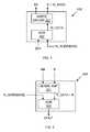
- FIG. 3is a block diagram illustrating a column 301 of N TCAM cells 300 0 - 300 (N ⁇ 1) , each of which is identical to TCAM cell 100 ( FIG. 1 ). Similar elements in FIGS. 1 and 3 are labeled with similar reference numbers. Thus, each TCAM cell 300 z includes corresponding SRAM cells 101 - 102 and match logic 103 . Note that word lines are not shown in FIG. 3 for purposes of clarity.
- the storage nodes of each TCAM cell 300 zare labeled XZ, XZ′, YZ and YZ′, wherein Z includes the integers from 0 to N ⁇ 1, inclusive.
- TCAM cell 300 0includes storage nodes X 0 , X 0 ′, Y 0 and Y 0 ′.
- the SRAM cells within TCAM cells 300 0 - 300 (N ⁇ 1)are connected to a complementary bit line pair, which includes bit lines B and B#.
- bit lines B and B#are twisted at a location 302 between the top and bottom of the column 301 . That is, for TCAM cells above twist location 302 , the storage nodes XZ and YZ are coupled to bit line B through the corresponding access transistors 115 and 125 , and the storage nodes XZ′ and YZ′ are coupled to the complementary bit line B# through the corresponding access transistors 116 and 126 .
- the storage nodes XZ′ and YZ′are coupled to bit line B through the corresponding access transistors 116 and 126 , and the storage nodes XZ and YZ are coupled to the complementary bit line B# through the corresponding access transistors 115 and 125 .
- bit lines B and B#are twisted at the half-way point of the column 301 , such that TCAM cells 300 0 - 300 (N/2 ⁇ 1) are located above the twist location 302 , and TCAM cells 300 (N/2) - 300 (N ⁇ 1) are located below the twist location 302 .
- twist location 302may be located at other positions along column 301 .
- twisting the bit lines B/B#advantageously minimizes the adverse affect of leakage current on read operations within column 301 .
- the match logic 103 within each of TCAM cells 300 0 - 300 (N ⁇ 1)is coupled to a complementary search line pair, which includes search line S and complementary search line S#. It is important to note that the search lines S and S# are not twisted in the present embodiment. Search operations are performed in the same manner described above in connection with FIG. 1 .
- TCAM cells 300 0 - 300 (N/2 ⁇ 1)which are located above the bit line twist location 302 (e.g., in the top half of column 301 ), are written with a first bit line polarity.
- TCAM cells 300 (N/2) - 300 (N ⁇ 1)which are located below the bit line twist location 302 (i.e., in the bottom half of column 301 ) are written with a second bit line polarity, opposite the first bit line polarity.
- the first bit line polarityis defined by the following example.
- a logic high voltage (V DD )is applied to bit line B and a logic low voltage (0 Volts) is applied to complementary bit line B# (and the corresponding word line is activated).
- V DDlogic high voltage
- V DDlogic low voltage
- V DDlogic high voltage
- the second bit line polarityis defined by the following example.
- a logic low voltage(0 Volts) is applied to bit line B
- a logic high voltageV DD is applied to complementary bit line B# (and the corresponding word line is activated).
- a logic ‘1’ data valueis written within each of the TCAM cells 300 0 - 300 (N ⁇ 1) by writing a logic ‘1’ value to the corresponding SRAM cell 101 and writing a logic ‘0’ value to the corresponding SRAM cell 102 .
- TCAM cells 300 0 and 300 (N/2)each store a logic ‘1’ data value.
- TCAM cell 300 (N ⁇ 1)stores a logic ‘0’ data value.
- a ‘don't care’ valueis written within each of the TCAM cells 300 0 - 300 (N ⁇ 1) by writing a logic ‘0’ value to the corresponding SRAM cells 101 and 102 .
- TCAM cell 300 (N/2 ⁇ 1)stores a ‘Don't Care’ value.
- FIG. 4is a block diagram of write control logic 400 that recognizes and applies the above-described first and second bit line polarities during write operations, in accordance with one embodiment of the present invention.
- Write control logic 400includes exclusive OR circuit 401 and write driver 402 .
- Exclusive OR circuit 401receives the write data value DIN to be written to the TCAM cell in column 301 .
- Exclusive OR circuit 401also receives the most significant bit (MSB) of the corresponding write address (W_ADDR).
- exclusive OR circuit 402provides the inverse of the write data value DIN to write driver 401 as the write data signal W_DATA.
- Write driver 401drives the bit lines B and B#, such that the bit line B is driven to a voltage that represents the same logic state as the write data signal W_DATA, and the complementary bit line B# is driven to a voltage that represents the opposite logic state. In this manner, write control logic 400 maintains the first and second bit line polarities described above.
- TCAM cells in column 301are read as follows in accordance with one embodiment of the present invention.
- TCAM cells 300 0 - 300 (N/2 ⁇ 1)which are located above the bit line twist location 302 (e.g., in the top half of column 301 ), are read with the first bit line polarity.
- TCAM cells 300 (N/2) - 300 (N ⁇ 1)which are located below the bit line twist location 302 (i.e., in the bottom half of column 301 ) are read with the second bit line polarity.
- each of the associated SRAM cells 101 and 102is read.
- Each SRAM cellis read in the following manner.
- Bit lines B/B#are initially precharged to a logic high voltage (V DD ), and the access transistors of the corresponding SRAM cell are turned on by activating the corresponding word line.
- V DDlogic high voltage
- the one of the storage nodes of the SRAM cellwill pull the corresponding bit line down toward ground, and the other one of the storage nodes of the SRAM cell will pull the corresponding bit line up toward V DD .
- a voltage differenceis created across the bit line pair B/B#. This voltage difference is detected by a sense amplifier (not shown).
- the first bit line polarityis used to identify the read data value. That is, a logic high voltage on bit line B and a logic low voltage on complementary bit line B# is recognized and reported as a logic ‘1’ data value; and a logic low voltage on bit line B and a logic high voltage on complementary bit line B# is recognized and reported as a logic ‘0’ data value.
- the second bit line polarityis used to identify the read data value. That is, a logic high voltage on bit line B and a logic low voltage on complementary bit line B# is recognized and reported as a logic ‘0’ data value; and a logic low voltage on bit line B and a logic high voltage on complementary bit line B# is recognized and reported as a logic ‘1’ data value.
- FIG. 5is a block diagram of read control logic 500 that recognizes and applies the above-described first and second bit line polarities during read operations, in accordance with one embodiment of the present invention.
- Read control logic 500includes sense amplifier 501 , which amplifies the voltage difference between the bit lines B/B# during a read operation.
- Sense amplifier 501provides a read data signal (R_DATA) having the logic state represented by the voltage developed on bit line B.
- the read data signal R_DATAis provided to exclusive OR circuit 502 , along with the most significant bit (MSB) of the corresponding read address (R_ADDR).
- worst case read conditionswill exist when one of the TCAM cells in a first half of the column 301 stores a logic ‘1’ data value, the remaining TCAM cells in the same half of the column 301 store ‘Don't Care’ values, and the TCAM cells in the other half of the column 301 do not store ‘Don't Care’ values.
- the leakage current during the read operationis equal to the leakage current through N ⁇ 1 SRAM cells (compared to 2N ⁇ 1 SRAM cells in the prior art TCAM column structure of FIG. 2 ).
- TCAM cell 300 0stores a logic ‘1’ data value (as illustrated in FIG. 3 )
- TCAM cells 300 1 - 300 249store ‘Don't Care’ values (as illustrated by TCAM cell 300 (N/2 ⁇ 1) in FIG. 3 )
- TCAM cells 300 250 - 300 499store logic ‘1’ data values (as illustrated by TCAM cell 300 (N/2) in FIG. 3 ) and/or logic ‘0’ data values (as illustrated by TCAM cell 300 (N ⁇ 1) in FIG. 3 ).
- the leakage currents through the SRAM cells 101 - 102 within TCAM cells 300 250 - 300 499 in the lower half of the column 301will be equally split between bit lines B and B#, such that the net effect of these leakage currents does not affect the voltage difference developed across bit lines B and B#.
- SRAM cell 101will have a leakage current through transistor 116 that tends to pull down the voltage on bit line B
- SRAM cell 102will have an opposing leakage current through transistor 125 that tends to pull down the voltage on complementary bit line B#.
- FIG. 6is a circuit diagram of a column 601 of TCAM cells 300 0 - 300 (N/2-1) , 600 (N/2) - 600 (N ⁇ 1) in accordance with an alternate embodiment of the present invention.
- TCAM cells 300 0 - 300 (N/2 ⁇ 1)have been described above in connection with FIG. 3 .
- TCAM cells 600 (N/2) - 600 (N ⁇ 1)are similar to TCAM cells 300 (N/2) - 300 (N ⁇ 1) , and are therefore labeled with similar reference numbers.
- TCAM cells 600 (N/2) - 600 (N ⁇ 1)are mirror images of TCAM cells 300 (N/2) - 300 (N ⁇ 1) . In this embodiment, neither search lines S and S# nor bit lines B and B# are twisted.
- Read and write operations to TCAM cells 300 0 - 300 (N/2 ⁇ 1) (which are located above location 302 )are performed with the first bit line polarity
- read and write operations to TCAM cells 600 (N/2) - 600 (N ⁇ 1) (which are located below location 302 )are performed with the second bit line polarity.
- Column 601exhibits the same worst case read conditions as column 301 .
Landscapes
- Static Random-Access Memory (AREA)
Abstract
Description
Claims (11)
Priority Applications (1)
| Application Number | Priority Date | Filing Date | Title |
|---|---|---|---|
| US12/431,332US7944724B2 (en) | 2009-04-28 | 2009-04-28 | Ternary content addressable memory having reduced leakage effects |
Applications Claiming Priority (1)
| Application Number | Priority Date | Filing Date | Title |
|---|---|---|---|
| US12/431,332US7944724B2 (en) | 2009-04-28 | 2009-04-28 | Ternary content addressable memory having reduced leakage effects |
Publications (2)
| Publication Number | Publication Date |
|---|---|
| US20100271854A1 US20100271854A1 (en) | 2010-10-28 |
| US7944724B2true US7944724B2 (en) | 2011-05-17 |
Family
ID=42991977
Family Applications (1)
| Application Number | Title | Priority Date | Filing Date |
|---|---|---|---|
| US12/431,332Active2029-07-08US7944724B2 (en) | 2009-04-28 | 2009-04-28 | Ternary content addressable memory having reduced leakage effects |
Country Status (1)
| Country | Link |
|---|---|
| US (1) | US7944724B2 (en) |
Cited By (10)
| Publication number | Priority date | Publication date | Assignee | Title |
|---|---|---|---|---|
| US8358524B1 (en) | 2007-06-29 | 2013-01-22 | Netlogic Microsystems, Inc. | Methods and circuits for limiting bit line leakage current in a content addressable memory (CAM) device |
| US8462532B1 (en) | 2010-08-31 | 2013-06-11 | Netlogic Microsystems, Inc. | Fast quaternary content addressable memory cell |
| US8553441B1 (en) | 2010-08-31 | 2013-10-08 | Netlogic Microsystems, Inc. | Ternary content addressable memory cell having two transistor pull-down stack |
| US8582338B1 (en) | 2010-08-31 | 2013-11-12 | Netlogic Microsystems, Inc. | Ternary content addressable memory cell having single transistor pull-down stack |
| US8625320B1 (en) | 2010-08-31 | 2014-01-07 | Netlogic Microsystems, Inc. | Quaternary content addressable memory cell having one transistor pull-down stack |
| US8773880B2 (en) | 2011-06-23 | 2014-07-08 | Netlogic Microsystems, Inc. | Content addressable memory array having virtual ground nodes |
| US8837188B1 (en) | 2011-06-23 | 2014-09-16 | Netlogic Microsystems, Inc. | Content addressable memory row having virtual ground and charge sharing |
| US8861271B1 (en)* | 2012-03-16 | 2014-10-14 | Cypress Semiconductor Corporation | High reliability non-volatile static random access memory devices, methods and systems |
| CN111128278A (en)* | 2018-10-30 | 2020-05-08 | 华为技术有限公司 | Content addressable memory, data processing method and network equipment |
| US11475953B1 (en)* | 2021-06-23 | 2022-10-18 | United Microelectronics Corp. | Semiconductor layout pattern and forming method thereof |
Families Citing this family (5)
| Publication number | Priority date | Publication date | Assignee | Title |
|---|---|---|---|---|
| US7920397B1 (en) | 2010-04-30 | 2011-04-05 | Netlogic Microsystems, Inc. | Memory device having bit line leakage compensation |
| KR20180028020A (en) | 2016-09-07 | 2018-03-15 | 르네사스 일렉트로닉스 가부시키가이샤 | Semiconductor device |
| US12327591B2 (en)* | 2021-04-09 | 2025-06-10 | Mediatek Singapore Pte. Ltd. | Method and apparatus for performing a MAC operation in a memory array |
| US12106822B2 (en) | 2021-07-16 | 2024-10-01 | Mediatek Singapore Pte. Ltd. | Memory array with programmable number of filters |
| JP7660532B2 (en)* | 2022-02-25 | 2025-04-11 | ルネサスエレクトロニクス株式会社 | Semiconductor Device |
Citations (87)
| Publication number | Priority date | Publication date | Assignee | Title |
|---|---|---|---|---|
| US4045781A (en) | 1976-02-13 | 1977-08-30 | Digital Equipment Corporation | Memory module with selectable byte addressing for digital data processing system |
| US4523301A (en) | 1982-06-04 | 1985-06-11 | Matsushita Electric Industrial Co., Ltd. | Associative memory |
| US5045899A (en) | 1989-12-01 | 1991-09-03 | Mitsubishi Denki Kabushiki Kaisha | Dynamic random access memory having stacked capacitor structure |
| US5062077A (en) | 1989-07-31 | 1991-10-29 | Kabushiki Kaisha Toshiba | Dynamic type semiconductor memory device |
| US5136543A (en) | 1989-05-12 | 1992-08-04 | Mitsubishi Denki Kabushiki Kaisha | Data descrambling in semiconductor memory device |
| US5140556A (en) | 1988-08-01 | 1992-08-18 | Oki Electric Industry Co., Ltd. | Semiconductor memory circuit having dummy cells connected to twisted bit lines |
| US5276649A (en) | 1989-03-16 | 1994-01-04 | Mitsubishi Denki Kabushiki Kaisha | Dynamic-type semiconductor memory device having staggered activation of column groups |
| US5280443A (en) | 1986-12-11 | 1994-01-18 | Mitsubishi Denki Kabushiki Kaisha | Bit line structure for semiconductor memory device |
| US5327372A (en) | 1992-01-17 | 1994-07-05 | Matsushita Electric Industrial Co., Ltd. | Semiconductor memory device |
| US5383159A (en) | 1992-09-17 | 1995-01-17 | Sharp Kabushiki Kaisha | Semiconductor memory device of alternately-activated open bit-line architecture |
| US5396449A (en) | 1993-12-21 | 1995-03-07 | International Business Machines Corporation | Fast content addressable memory with reduced power consumption |
| US5440715A (en) | 1990-06-27 | 1995-08-08 | Advanced Micro Devices, Inc. | Method and apparatus for expanding the width of a content addressable memory using a continuation bit |
| US5446685A (en) | 1993-02-23 | 1995-08-29 | Intergraph Corporation | Pulsed ground circuit for CAM and PAL memories |
| US5483480A (en) | 1993-07-22 | 1996-01-09 | Kawasaki Steel Corporation | Method of using associative memories and an associative memory |
| US5488583A (en) | 1994-09-22 | 1996-01-30 | Micron Technology, Inc. | Memory integrated circuits having on-chip topology logic driver, and methods for testing and producing such memory integrated circuits |
| US5499218A (en) | 1995-01-31 | 1996-03-12 | Goldstar Electron Co., Ltd. | Method for driving bit line selecting signals |
| US5517441A (en) | 1994-12-14 | 1996-05-14 | International Business Machines Corporation | Content addressable memory circuitry and method of operation |
| US5534732A (en) | 1994-08-15 | 1996-07-09 | International Business Machines Corporation | Single twist layout and method for paired line conductors of integrated circuits |
| US5649126A (en) | 1995-12-04 | 1997-07-15 | Sun Microsystems, Inc. | Parallel signal bus with reduced miller effect capacitance |
| US5699288A (en) | 1996-07-18 | 1997-12-16 | International Business Machines Corporation | Compare circuit for content-addressable memories |
| US5706224A (en) | 1996-10-10 | 1998-01-06 | Quality Semiconductor, Inc. | Content addressable memory and random access memory partition circuit |
| US5740097A (en) | 1994-11-28 | 1998-04-14 | International Business Machines Corporation | Content-addressable-memory control circuit |
| US5818786A (en) | 1995-05-24 | 1998-10-06 | Kawasaki Steel Corporation | Layout method of semiconductor memory and content-addressable memory |
| US5852569A (en) | 1997-05-20 | 1998-12-22 | Quality Semiconductor, Inc. | Content addressable memory multiple match detection circuit |
| US5859791A (en) | 1997-01-09 | 1999-01-12 | Northern Telecom Limited | Content addressable memory |
| US5936873A (en) | 1997-09-30 | 1999-08-10 | Sun Microsystems, Inc. | Single ended match sense amplifier |
| US5964857A (en) | 1997-05-30 | 1999-10-12 | Quality Semiconductor, Inc. | Priority encoder for a content addressable memory system |
| US5966319A (en) | 1997-07-15 | 1999-10-12 | Mitsubishi Denki Kabushiki Kaisha | Static memory device allowing correct data reading |
| US5978246A (en) | 1997-09-08 | 1999-11-02 | Nec Corporation | Content addressable memory device |
| US6044005A (en) | 1999-02-03 | 2000-03-28 | Sibercore Technologies Incorporated | Content addressable memory storage device |
| US6075729A (en) | 1997-09-05 | 2000-06-13 | Hitachi, Ltd. | High-speed static random access memory |
| US6101116A (en) | 1999-06-30 | 2000-08-08 | Integrated Device Technology, Inc. | Six transistor content addressable memory cell |
| US6101115A (en) | 1998-08-07 | 2000-08-08 | Cisco Technology, Inc. | CAM match line precharge |
| US6125049A (en) | 1999-01-05 | 2000-09-26 | Netlogic Microsystems, Inc. | Match line control circuit for content addressable memory |
| US6128207A (en) | 1998-11-02 | 2000-10-03 | Integrated Device Technology, Inc. | Low-power content addressable memory cell |
| US6166939A (en) | 1999-07-12 | 2000-12-26 | Net Logic Microsystems | Method and apparatus for selective match line pre-charging in a content addressable memory |
| US6175514B1 (en) | 1999-01-15 | 2001-01-16 | Fast-Chip, Inc. | Content addressable memory device |
| US6191970B1 (en) | 1999-09-09 | 2001-02-20 | Netlogic Microsystems, Inc. | Selective match line discharging in a partitioned content addressable memory array |
| US6195278B1 (en) | 1999-12-30 | 2001-02-27 | Nortel Networks Limited | Content addressable memory cells and words |
| US6243280B1 (en) | 1999-09-09 | 2001-06-05 | Netlogic Microsystems, Inc. | Selective match line pre-charging in a partitioned content addressable memory array |
| US6243281B1 (en) | 2000-06-14 | 2001-06-05 | Netlogic Microsystems, Inc. | Method and apparatus for accessing a segment of CAM cells in an intra-row configurable CAM system |
| US6246601B1 (en) | 2000-06-14 | 2001-06-12 | Netlogic Microsystems, Inc. | Method and apparatus for using an inter-row configurable content addressable memory |
| US6252789B1 (en) | 2000-06-14 | 2001-06-26 | Netlogic Microsystems, Inc. | Inter-row configurability of content addressable memory |
| US6256241B1 (en) | 2000-03-30 | 2001-07-03 | Intel Corporation | Short write test mode for testing static memory cells |
| US6256216B1 (en) | 2000-05-18 | 2001-07-03 | Integrated Device Technology, Inc. | Cam array with minimum cell size |
| US6262907B1 (en) | 2000-05-18 | 2001-07-17 | Integrated Device Technology, Inc. | Ternary CAM array |
| US6262929B1 (en) | 1999-02-05 | 2001-07-17 | International Business Machines Corporation | Pre-charging circuit and method for a word match line of a content add ressable memory (CAM) |
| US6282113B1 (en) | 1999-09-29 | 2001-08-28 | International Business Machines Corporation | Four F-squared gapless dual layer bitline DRAM array architecture |
| US6292383B1 (en) | 2000-04-27 | 2001-09-18 | Stmicroelectronics, Inc. | Redundant memory cell for dynamic random access memories having twisted bit line architectures |
| US6324087B1 (en) | 2000-06-08 | 2001-11-27 | Netlogic Microsystems, Inc. | Method and apparatus for partitioning a content addressable memory device |
| US6331942B1 (en) | 2000-09-09 | 2001-12-18 | Tality, L.P. | Content addressable memory cell and design methodology utilizing grounding circuitry |
| US6341079B1 (en) | 2001-05-23 | 2002-01-22 | International Business Machines Corporation | Content addressable memory device |
| US6343029B1 (en) | 2001-02-13 | 2002-01-29 | Silicon Access Networks, Inc. | Charge shared match line differential generation for CAM |
| US6349049B1 (en) | 2001-03-22 | 2002-02-19 | Sun Microsystems, Inc. | High speed low power content addressable memory |
| US6370613B1 (en) | 1999-07-27 | 2002-04-09 | Integrated Device Technology, Inc. | Content addressable memory with longest match detect |
| US6373738B1 (en) | 2000-11-20 | 2002-04-16 | International Business Machines Corporation | Low power CAM match line circuit |
| US6430074B1 (en) | 1999-09-09 | 2002-08-06 | Netlogic Mircosystems, Inc. | Selective look-ahead match line pre-charging in a partitioned content addressable memory array |
| US6442061B1 (en) | 2001-02-14 | 2002-08-27 | Lsi Logic Corporation | Single channel four transistor SRAM |
| US6452822B1 (en) | 2001-04-26 | 2002-09-17 | International Business Machines Corporation | Segmented match line arrangement for content addressable memory |
| US6483733B2 (en) | 1999-03-31 | 2002-11-19 | Mosaid Technologies Incorporated | Dynamic content addressable memory cell |
| US6499081B1 (en) | 1999-02-23 | 2002-12-24 | Netlogic Microsystems, Inc. | Method and apparatus for determining a longest prefix match in a segmented content addressable memory device |
| US6500706B1 (en) | 2001-03-19 | 2002-12-31 | Taiwan Semiconductor Manufacturing Company | Bit-line interconnection scheme for eliminating coupling noise in stack DRAM cell with capacitor under bit-line (CUB) in stand-alone or embedded DRAM |
| US20030002351A1 (en)* | 2001-06-23 | 2003-01-02 | Peter Beer | Integrated memory circuit and method for reading a data item from a memory cell |
| US6512682B2 (en) | 2001-03-29 | 2003-01-28 | Intel Corporation | Power supply with interface to determine power requirements of devices coupled thereto |
| US20030070039A1 (en) | 2001-09-28 | 2003-04-10 | Peter Gillingham | Circuit and method for performing variable width searches in a content addressable memory |
| US6560670B1 (en) | 2000-06-14 | 2003-05-06 | Netlogic Microsystems, Inc. | Inter-row configurability of content addressable memory |
| US6563727B1 (en)* | 2002-07-31 | 2003-05-13 | Alan Roth | Method and structure for reducing noise effects in content addressable memories |
| US6570794B1 (en) | 2001-12-27 | 2003-05-27 | Infineon Technologies North America Corp. | Twisted bit-line compensation for DRAM having redundancy |
| US20030123269A1 (en) | 2001-12-31 | 2003-07-03 | Peter Gillingham | Circuit and method for reducing power usage in a content addressable memory |
| US6597596B2 (en) | 2001-06-11 | 2003-07-22 | International Business Machines Corporation | Content addressable memory having cascaded sub-entry architecture |
| US6597594B2 (en) | 2000-03-17 | 2003-07-22 | Silicon Aquarius, Inc. | Content addressable memory cells and systems and devices using the same |
| US6646900B2 (en) | 2001-10-31 | 2003-11-11 | Kawasaki Microelectronics, Inc. | Ternary content addressable memory with data and mask data settable therewithin by one write cycle |
| US6657880B1 (en) | 2002-12-04 | 2003-12-02 | Virtual Silicon Technology, Inc. | SRAM bit line architecture |
| US6697277B2 (en) | 2001-08-06 | 2004-02-24 | International Business Machines Corporation | Content addressable memory (CAM) having a match line circuit with selectively adjustable pull-up impedances |
| US6785179B1 (en) | 2003-06-19 | 2004-08-31 | Arm Limited | Charge sharing between bit lines within a memory circuit to increase recharge speed |
| US6795325B1 (en) | 2003-03-26 | 2004-09-21 | Renesas Technology Corp. | Semiconductor memory |
| US6804134B1 (en) | 2002-04-10 | 2004-10-12 | Integrated Device Technology, Inc. | Content addressable memory (CAM) devices having CAM array blocks therein that conserve bit line power during staged compare operations |
| US6803610B2 (en)* | 2002-09-30 | 2004-10-12 | Mosaid Technologies Incorporated | Optimized memory cell physical arrangement |
| US6807077B2 (en)* | 2002-12-13 | 2004-10-19 | Renesas Technology Corp. | Content addressable memory capable of stably storing ternary data |
| US6879504B1 (en) | 2001-02-08 | 2005-04-12 | Integrated Device Technology, Inc. | Content addressable memory (CAM) devices having error detection and correction control circuits therein and methods of operating same |
| US6888730B2 (en) | 2001-04-03 | 2005-05-03 | Mosaid Technologies Incorporated | Content addressable memory cell |
| US6901000B1 (en) | 2003-05-30 | 2005-05-31 | Netlogic Microsystems Inc | Content addressable memory with multi-ported compare and word length selection |
| US6900999B1 (en)* | 2003-06-30 | 2005-05-31 | Integrated Device Technology, Inc. | Ternary content addressable memory (TCAM) cells with small footprint size and efficient layout aspect ratio |
| US6906937B1 (en) | 2003-03-21 | 2005-06-14 | Netlogic Microsystems, Inc. | Bit line control circuit for a content addressable memory |
| US7277309B1 (en)* | 2004-03-26 | 2007-10-02 | Netlogic Microsystems, Inc. | Interlocking memory/logic cell layout and method of manufacture |
| US7319602B1 (en)* | 2004-07-01 | 2008-01-15 | Netlogic Microsystems, Inc | Content addressable memory with twisted data lines |
| US7355890B1 (en)* | 2006-10-26 | 2008-04-08 | Integrated Device Technology, Inc. | Content addressable memory (CAM) devices having NAND-type compare circuits |
- 2009
- 2009-04-28USUS12/431,332patent/US7944724B2/enactiveActive
Patent Citations (98)
| Publication number | Priority date | Publication date | Assignee | Title |
|---|---|---|---|---|
| US4045781A (en) | 1976-02-13 | 1977-08-30 | Digital Equipment Corporation | Memory module with selectable byte addressing for digital data processing system |
| US4523301A (en) | 1982-06-04 | 1985-06-11 | Matsushita Electric Industrial Co., Ltd. | Associative memory |
| US5461589A (en) | 1986-12-11 | 1995-10-24 | Mitsubishi Denki Kabushiki Kaisha | Bit line structure for semiconductor memory device with bank separation at cross-over regions |
| US5280443A (en) | 1986-12-11 | 1994-01-18 | Mitsubishi Denki Kabushiki Kaisha | Bit line structure for semiconductor memory device |
| US5550769A (en) | 1986-12-11 | 1996-08-27 | Mitsubishi Denki Kabushiki Kaisha | Bit line structure for semiconductor memory device |
| US5416734A (en) | 1986-12-11 | 1995-05-16 | Mitsubishi Denki Kabushiki Kaisha | Bit line structure for semiconductor memory device |
| US5140556A (en) | 1988-08-01 | 1992-08-18 | Oki Electric Industry Co., Ltd. | Semiconductor memory circuit having dummy cells connected to twisted bit lines |
| US5276649A (en) | 1989-03-16 | 1994-01-04 | Mitsubishi Denki Kabushiki Kaisha | Dynamic-type semiconductor memory device having staggered activation of column groups |
| US5136543A (en) | 1989-05-12 | 1992-08-04 | Mitsubishi Denki Kabushiki Kaisha | Data descrambling in semiconductor memory device |
| US5062077A (en) | 1989-07-31 | 1991-10-29 | Kabushiki Kaisha Toshiba | Dynamic type semiconductor memory device |
| US5045899A (en) | 1989-12-01 | 1991-09-03 | Mitsubishi Denki Kabushiki Kaisha | Dynamic random access memory having stacked capacitor structure |
| US5440715A (en) | 1990-06-27 | 1995-08-08 | Advanced Micro Devices, Inc. | Method and apparatus for expanding the width of a content addressable memory using a continuation bit |
| US5327372A (en) | 1992-01-17 | 1994-07-05 | Matsushita Electric Industrial Co., Ltd. | Semiconductor memory device |
| US5383159A (en) | 1992-09-17 | 1995-01-17 | Sharp Kabushiki Kaisha | Semiconductor memory device of alternately-activated open bit-line architecture |
| US5598115A (en) | 1993-02-23 | 1997-01-28 | Intergraph Corporation | Comparator cell for use in a content addressable memory |
| US5446685A (en) | 1993-02-23 | 1995-08-29 | Intergraph Corporation | Pulsed ground circuit for CAM and PAL memories |
| US5483480A (en) | 1993-07-22 | 1996-01-09 | Kawasaki Steel Corporation | Method of using associative memories and an associative memory |
| US5396449A (en) | 1993-12-21 | 1995-03-07 | International Business Machines Corporation | Fast content addressable memory with reduced power consumption |
| US5534732A (en) | 1994-08-15 | 1996-07-09 | International Business Machines Corporation | Single twist layout and method for paired line conductors of integrated circuits |
| US5488583A (en) | 1994-09-22 | 1996-01-30 | Micron Technology, Inc. | Memory integrated circuits having on-chip topology logic driver, and methods for testing and producing such memory integrated circuits |
| US5740097A (en) | 1994-11-28 | 1998-04-14 | International Business Machines Corporation | Content-addressable-memory control circuit |
| US5517441A (en) | 1994-12-14 | 1996-05-14 | International Business Machines Corporation | Content addressable memory circuitry and method of operation |
| US5499218A (en) | 1995-01-31 | 1996-03-12 | Goldstar Electron Co., Ltd. | Method for driving bit line selecting signals |
| US5818786A (en) | 1995-05-24 | 1998-10-06 | Kawasaki Steel Corporation | Layout method of semiconductor memory and content-addressable memory |
| US5649126A (en) | 1995-12-04 | 1997-07-15 | Sun Microsystems, Inc. | Parallel signal bus with reduced miller effect capacitance |
| US5699288A (en) | 1996-07-18 | 1997-12-16 | International Business Machines Corporation | Compare circuit for content-addressable memories |
| US5706224A (en) | 1996-10-10 | 1998-01-06 | Quality Semiconductor, Inc. | Content addressable memory and random access memory partition circuit |
| US5859791A (en) | 1997-01-09 | 1999-01-12 | Northern Telecom Limited | Content addressable memory |
| US5852569A (en) | 1997-05-20 | 1998-12-22 | Quality Semiconductor, Inc. | Content addressable memory multiple match detection circuit |
| US5964857A (en) | 1997-05-30 | 1999-10-12 | Quality Semiconductor, Inc. | Priority encoder for a content addressable memory system |
| US5966319A (en) | 1997-07-15 | 1999-10-12 | Mitsubishi Denki Kabushiki Kaisha | Static memory device allowing correct data reading |
| US6075729A (en) | 1997-09-05 | 2000-06-13 | Hitachi, Ltd. | High-speed static random access memory |
| US5978246A (en) | 1997-09-08 | 1999-11-02 | Nec Corporation | Content addressable memory device |
| US5936873A (en) | 1997-09-30 | 1999-08-10 | Sun Microsystems, Inc. | Single ended match sense amplifier |
| US6101115A (en) | 1998-08-07 | 2000-08-08 | Cisco Technology, Inc. | CAM match line precharge |
| US6240001B1 (en) | 1998-08-07 | 2001-05-29 | Cisco Technology, Inc. | CAM match line precharge |
| US6128207A (en) | 1998-11-02 | 2000-10-03 | Integrated Device Technology, Inc. | Low-power content addressable memory cell |
| US6125049A (en) | 1999-01-05 | 2000-09-26 | Netlogic Microsystems, Inc. | Match line control circuit for content addressable memory |
| US6147891A (en) | 1999-01-05 | 2000-11-14 | Netlogic Microsystems | Match line control circuit for content addressable memory |
| US6362993B1 (en) | 1999-01-15 | 2002-03-26 | Fast-Chip Incorporated | Content addressable memory device |
| US6175514B1 (en) | 1999-01-15 | 2001-01-16 | Fast-Chip, Inc. | Content addressable memory device |
| US6044005A (en) | 1999-02-03 | 2000-03-28 | Sibercore Technologies Incorporated | Content addressable memory storage device |
| US6262929B1 (en) | 1999-02-05 | 2001-07-17 | International Business Machines Corporation | Pre-charging circuit and method for a word match line of a content add ressable memory (CAM) |
| US6499081B1 (en) | 1999-02-23 | 2002-12-24 | Netlogic Microsystems, Inc. | Method and apparatus for determining a longest prefix match in a segmented content addressable memory device |
| US6483733B2 (en) | 1999-03-31 | 2002-11-19 | Mosaid Technologies Incorporated | Dynamic content addressable memory cell |
| US6101116A (en) | 1999-06-30 | 2000-08-08 | Integrated Device Technology, Inc. | Six transistor content addressable memory cell |
| US6166939A (en) | 1999-07-12 | 2000-12-26 | Net Logic Microsystems | Method and apparatus for selective match line pre-charging in a content addressable memory |
| US6370613B1 (en) | 1999-07-27 | 2002-04-09 | Integrated Device Technology, Inc. | Content addressable memory with longest match detect |
| US6243280B1 (en) | 1999-09-09 | 2001-06-05 | Netlogic Microsystems, Inc. | Selective match line pre-charging in a partitioned content addressable memory array |
| US6191969B1 (en) | 1999-09-09 | 2001-02-20 | Net Logic Microsystems, Inc. | Selective match line discharging in a partitioned content addressable memory array |
| US6191970B1 (en) | 1999-09-09 | 2001-02-20 | Netlogic Microsystems, Inc. | Selective match line discharging in a partitioned content addressable memory array |
| US6430074B1 (en) | 1999-09-09 | 2002-08-06 | Netlogic Mircosystems, Inc. | Selective look-ahead match line pre-charging in a partitioned content addressable memory array |
| US6282113B1 (en) | 1999-09-29 | 2001-08-28 | International Business Machines Corporation | Four F-squared gapless dual layer bitline DRAM array architecture |
| US6195278B1 (en) | 1999-12-30 | 2001-02-27 | Nortel Networks Limited | Content addressable memory cells and words |
| US6597594B2 (en) | 2000-03-17 | 2003-07-22 | Silicon Aquarius, Inc. | Content addressable memory cells and systems and devices using the same |
| US6256241B1 (en) | 2000-03-30 | 2001-07-03 | Intel Corporation | Short write test mode for testing static memory cells |
| US6292383B1 (en) | 2000-04-27 | 2001-09-18 | Stmicroelectronics, Inc. | Redundant memory cell for dynamic random access memories having twisted bit line architectures |
| US6262907B1 (en) | 2000-05-18 | 2001-07-17 | Integrated Device Technology, Inc. | Ternary CAM array |
| US6256216B1 (en) | 2000-05-18 | 2001-07-03 | Integrated Device Technology, Inc. | Cam array with minimum cell size |
| US6324087B1 (en) | 2000-06-08 | 2001-11-27 | Netlogic Microsystems, Inc. | Method and apparatus for partitioning a content addressable memory device |
| US6246601B1 (en) | 2000-06-14 | 2001-06-12 | Netlogic Microsystems, Inc. | Method and apparatus for using an inter-row configurable content addressable memory |
| US6560670B1 (en) | 2000-06-14 | 2003-05-06 | Netlogic Microsystems, Inc. | Inter-row configurability of content addressable memory |
| US6243281B1 (en) | 2000-06-14 | 2001-06-05 | Netlogic Microsystems, Inc. | Method and apparatus for accessing a segment of CAM cells in an intra-row configurable CAM system |
| US6252789B1 (en) | 2000-06-14 | 2001-06-26 | Netlogic Microsystems, Inc. | Inter-row configurability of content addressable memory |
| US6331942B1 (en) | 2000-09-09 | 2001-12-18 | Tality, L.P. | Content addressable memory cell and design methodology utilizing grounding circuitry |
| US6373738B1 (en) | 2000-11-20 | 2002-04-16 | International Business Machines Corporation | Low power CAM match line circuit |
| US6879504B1 (en) | 2001-02-08 | 2005-04-12 | Integrated Device Technology, Inc. | Content addressable memory (CAM) devices having error detection and correction control circuits therein and methods of operating same |
| US6343029B1 (en) | 2001-02-13 | 2002-01-29 | Silicon Access Networks, Inc. | Charge shared match line differential generation for CAM |
| US6442061B1 (en) | 2001-02-14 | 2002-08-27 | Lsi Logic Corporation | Single channel four transistor SRAM |
| US6500706B1 (en) | 2001-03-19 | 2002-12-31 | Taiwan Semiconductor Manufacturing Company | Bit-line interconnection scheme for eliminating coupling noise in stack DRAM cell with capacitor under bit-line (CUB) in stand-alone or embedded DRAM |
| US6349049B1 (en) | 2001-03-22 | 2002-02-19 | Sun Microsystems, Inc. | High speed low power content addressable memory |
| US6512682B2 (en) | 2001-03-29 | 2003-01-28 | Intel Corporation | Power supply with interface to determine power requirements of devices coupled thereto |
| US6888730B2 (en) | 2001-04-03 | 2005-05-03 | Mosaid Technologies Incorporated | Content addressable memory cell |
| US6452822B1 (en) | 2001-04-26 | 2002-09-17 | International Business Machines Corporation | Segmented match line arrangement for content addressable memory |
| US6341079B1 (en) | 2001-05-23 | 2002-01-22 | International Business Machines Corporation | Content addressable memory device |
| US6597596B2 (en) | 2001-06-11 | 2003-07-22 | International Business Machines Corporation | Content addressable memory having cascaded sub-entry architecture |
| US20030002351A1 (en)* | 2001-06-23 | 2003-01-02 | Peter Beer | Integrated memory circuit and method for reading a data item from a memory cell |
| US6697277B2 (en) | 2001-08-06 | 2004-02-24 | International Business Machines Corporation | Content addressable memory (CAM) having a match line circuit with selectively adjustable pull-up impedances |
| US6708250B2 (en) | 2001-09-28 | 2004-03-16 | Mosaid Technologies Incorporated | Circuit and method for performing variable width searches in a content addressable memory |
| US20030070039A1 (en) | 2001-09-28 | 2003-04-10 | Peter Gillingham | Circuit and method for performing variable width searches in a content addressable memory |
| US6646900B2 (en) | 2001-10-31 | 2003-11-11 | Kawasaki Microelectronics, Inc. | Ternary content addressable memory with data and mask data settable therewithin by one write cycle |
| US6570794B1 (en) | 2001-12-27 | 2003-05-27 | Infineon Technologies North America Corp. | Twisted bit-line compensation for DRAM having redundancy |
| US20030123269A1 (en) | 2001-12-31 | 2003-07-03 | Peter Gillingham | Circuit and method for reducing power usage in a content addressable memory |
| US6804134B1 (en) | 2002-04-10 | 2004-10-12 | Integrated Device Technology, Inc. | Content addressable memory (CAM) devices having CAM array blocks therein that conserve bit line power during staged compare operations |
| US6563727B1 (en)* | 2002-07-31 | 2003-05-13 | Alan Roth | Method and structure for reducing noise effects in content addressable memories |
| US6803610B2 (en)* | 2002-09-30 | 2004-10-12 | Mosaid Technologies Incorporated | Optimized memory cell physical arrangement |
| US6657880B1 (en) | 2002-12-04 | 2003-12-02 | Virtual Silicon Technology, Inc. | SRAM bit line architecture |
| US6807077B2 (en)* | 2002-12-13 | 2004-10-19 | Renesas Technology Corp. | Content addressable memory capable of stably storing ternary data |
| US6906937B1 (en) | 2003-03-21 | 2005-06-14 | Netlogic Microsystems, Inc. | Bit line control circuit for a content addressable memory |
| US7154764B2 (en) | 2003-03-21 | 2006-12-26 | Netlogic Microsystems, Inc. | Method of controlling a bit line for a content addressable memory |
| US6795325B1 (en) | 2003-03-26 | 2004-09-21 | Renesas Technology Corp. | Semiconductor memory |
| US6901000B1 (en) | 2003-05-30 | 2005-05-31 | Netlogic Microsystems Inc | Content addressable memory with multi-ported compare and word length selection |
| US6785179B1 (en) | 2003-06-19 | 2004-08-31 | Arm Limited | Charge sharing between bit lines within a memory circuit to increase recharge speed |
| US6900999B1 (en)* | 2003-06-30 | 2005-05-31 | Integrated Device Technology, Inc. | Ternary content addressable memory (TCAM) cells with small footprint size and efficient layout aspect ratio |
| US7277309B1 (en)* | 2004-03-26 | 2007-10-02 | Netlogic Microsystems, Inc. | Interlocking memory/logic cell layout and method of manufacture |
| US7319602B1 (en)* | 2004-07-01 | 2008-01-15 | Netlogic Microsystems, Inc | Content addressable memory with twisted data lines |
| US7545661B2 (en)* | 2004-07-01 | 2009-06-09 | Netlogic Microsystems, Inc. | Content addressable memory with twisted data lines |
| US7355890B1 (en)* | 2006-10-26 | 2008-04-08 | Integrated Device Technology, Inc. | Content addressable memory (CAM) devices having NAND-type compare circuits |
Cited By (14)
| Publication number | Priority date | Publication date | Assignee | Title |
|---|---|---|---|---|
| US8358524B1 (en) | 2007-06-29 | 2013-01-22 | Netlogic Microsystems, Inc. | Methods and circuits for limiting bit line leakage current in a content addressable memory (CAM) device |
| US8724359B2 (en) | 2007-06-29 | 2014-05-13 | Netlogic Microsystems, Inc. | Methods and circuits for limiting bit line leakage current in a content addressable memory (CAM) device |
| US8462532B1 (en) | 2010-08-31 | 2013-06-11 | Netlogic Microsystems, Inc. | Fast quaternary content addressable memory cell |
| US8553441B1 (en) | 2010-08-31 | 2013-10-08 | Netlogic Microsystems, Inc. | Ternary content addressable memory cell having two transistor pull-down stack |
| US8582338B1 (en) | 2010-08-31 | 2013-11-12 | Netlogic Microsystems, Inc. | Ternary content addressable memory cell having single transistor pull-down stack |
| US8625320B1 (en) | 2010-08-31 | 2014-01-07 | Netlogic Microsystems, Inc. | Quaternary content addressable memory cell having one transistor pull-down stack |
| US8773880B2 (en) | 2011-06-23 | 2014-07-08 | Netlogic Microsystems, Inc. | Content addressable memory array having virtual ground nodes |
| US8837188B1 (en) | 2011-06-23 | 2014-09-16 | Netlogic Microsystems, Inc. | Content addressable memory row having virtual ground and charge sharing |
| US8861271B1 (en)* | 2012-03-16 | 2014-10-14 | Cypress Semiconductor Corporation | High reliability non-volatile static random access memory devices, methods and systems |
| US9570152B1 (en) | 2012-03-16 | 2017-02-14 | Cypress Semiconductor Corporation | High reliability non-volatile static random access memory devices, methods and systems |
| CN111128278A (en)* | 2018-10-30 | 2020-05-08 | 华为技术有限公司 | Content addressable memory, data processing method and network equipment |
| CN111128278B (en)* | 2018-10-30 | 2021-08-27 | 华为技术有限公司 | Content addressable memory, data processing method and network equipment |
| US11468933B2 (en) | 2018-10-30 | 2022-10-11 | Huawei Technologies Co., Ltd. | Content addressable memory, data processing method, and network device |
| US11475953B1 (en)* | 2021-06-23 | 2022-10-18 | United Microelectronics Corp. | Semiconductor layout pattern and forming method thereof |
Also Published As
| Publication number | Publication date |
|---|---|
| US20100271854A1 (en) | 2010-10-28 |
Similar Documents
| Publication | Publication Date | Title |
|---|---|---|
| US7944724B2 (en) | Ternary content addressable memory having reduced leakage effects | |
| US6781857B1 (en) | Content addressable memory (CAM) devices that utilize multi-port CAM cells and control logic to support multiple overlapping search cycles that are asynchronously timed relative to each other | |
| US6657878B2 (en) | Content addressable memory (CAM) devices having reliable column redundancy characteristics and methods of operating same | |
| US6421265B1 (en) | DRAM-based CAM cell using 3T or 4T DRAM cells | |
| US6744688B2 (en) | Searchline control circuit and power reduction method | |
| US8462532B1 (en) | Fast quaternary content addressable memory cell | |
| US7440313B2 (en) | Two-port SRAM having improved write operation | |
| US6552944B2 (en) | Single bitline direct sensing architecture for high speed memory device | |
| US7298635B1 (en) | Content addressable memory (CAM) cell with single ended write multiplexing | |
| US7903483B2 (en) | Integrated circuit having memory with configurable read/write operations and method therefor | |
| US20070115739A1 (en) | Output circuit of a memory and method thereof | |
| US6906937B1 (en) | Bit line control circuit for a content addressable memory | |
| US6101116A (en) | Six transistor content addressable memory cell | |
| US7525854B2 (en) | Memory output circuit and method thereof | |
| US5043945A (en) | Memory with improved bit line and write data line equalization | |
| US8659926B1 (en) | PMC-based non-volatile CAM | |
| CN101154442A (en) | Static random access memory macro and dual port static random access memory device | |
| US6845025B1 (en) | Word line driver circuit for a content addressable memory | |
| US6504775B1 (en) | Bitline precharge | |
| JP2004039209A (en) | Ternary content search memory device | |
| US7113415B1 (en) | Match line pre-charging in a content addressable memory having configurable rows | |
| US20240371437A1 (en) | Memory device | |
| US6982912B2 (en) | Semiconductor memory device | |
| US20250264992A1 (en) | Sensing within an embedded dynamic random access memories (drams) having reference cells | |
| US20060092720A1 (en) | Semiconductor memory |
Legal Events
| Date | Code | Title | Description |
|---|---|---|---|
| AS | Assignment | Owner name:INTEGRATED DEVICE TECHNOLOGY, INC., CALIFORNIA Free format text:ASSIGNMENT OF ASSIGNORS INTEREST;ASSIGNOR:CHU, SCOTT;REEL/FRAME:022605/0701 Effective date:20090427 | |
| AS | Assignment | Owner name:SILICON VALLEY BANK, CALIFORNIA Free format text:SECURITY AGREEMENT;ASSIGNORS:NETLOGIC MICROSYSTEMS, INC.;NETLOGIC MICROSYSTEMS INTERNATIONAL LIMITED;NETLOGIC MICROSYSTEMS CAYMANS LIMITED;REEL/FRAME:022973/0710 Effective date:20090717 | |
| AS | Assignment | Owner name:NETLOGIC MICROSYSTEMS, INC., CALIFORNIA Free format text:ASSIGNMENT OF ASSIGNORS INTEREST;ASSIGNOR:INTEGRATED DEVICE TECHNOLOGY, INC.;REEL/FRAME:022997/0671 Effective date:20090717 | |
| FEPP | Fee payment procedure | Free format text:PAYER NUMBER DE-ASSIGNED (ORIGINAL EVENT CODE: RMPN); ENTITY STATUS OF PATENT OWNER: LARGE ENTITY | |
| FEPP | Fee payment procedure | Free format text:PAYOR NUMBER ASSIGNED (ORIGINAL EVENT CODE: ASPN); ENTITY STATUS OF PATENT OWNER: LARGE ENTITY | |
| STCF | Information on status: patent grant | Free format text:PATENTED CASE | |
| AS | Assignment | Owner name:NETLOGIC MICROSYSTEMS INTERNATIONAL LIMITED, CALIF Free format text:RELEASE BY SECURED PARTY;ASSIGNOR:SILICON VALLEY BANK;REEL/FRAME:026830/0141 Effective date:20110826 Owner name:NETLOGIC MICROSYSTEMS CAYMANS LIMITED, CALIFORNIA Free format text:RELEASE BY SECURED PARTY;ASSIGNOR:SILICON VALLEY BANK;REEL/FRAME:026830/0141 Effective date:20110826 Owner name:NETLOGIC MICROSYSTEMS, INC., CALIFORNIA Free format text:RELEASE BY SECURED PARTY;ASSIGNOR:SILICON VALLEY BANK;REEL/FRAME:026830/0141 Effective date:20110826 | |
| FPAY | Fee payment | Year of fee payment:4 | |
| SULP | Surcharge for late payment | ||
| AS | Assignment | Owner name:BROADCOM CORPORATION, CALIFORNIA Free format text:ASSIGNMENT OF ASSIGNORS INTEREST;ASSIGNOR:NETLOGIC I LLC;REEL/FRAME:035443/0763 Effective date:20150327 Owner name:NETLOGIC I LLC, DELAWARE Free format text:CHANGE OF NAME;ASSIGNOR:NETLOGIC MICROSYSTEMS, INC.;REEL/FRAME:035443/0824 Effective date:20130123 | |
| AS | Assignment | Owner name:BANK OF AMERICA, N.A., AS COLLATERAL AGENT, NORTH CAROLINA Free format text:PATENT SECURITY AGREEMENT;ASSIGNOR:BROADCOM CORPORATION;REEL/FRAME:037806/0001 Effective date:20160201 Owner name:BANK OF AMERICA, N.A., AS COLLATERAL AGENT, NORTH Free format text:PATENT SECURITY AGREEMENT;ASSIGNOR:BROADCOM CORPORATION;REEL/FRAME:037806/0001 Effective date:20160201 | |
| AS | Assignment | Owner name:AVAGO TECHNOLOGIES GENERAL IP (SINGAPORE) PTE. LTD., SINGAPORE Free format text:ASSIGNMENT OF ASSIGNORS INTEREST;ASSIGNOR:BROADCOM CORPORATION;REEL/FRAME:041706/0001 Effective date:20170120 Owner name:AVAGO TECHNOLOGIES GENERAL IP (SINGAPORE) PTE. LTD Free format text:ASSIGNMENT OF ASSIGNORS INTEREST;ASSIGNOR:BROADCOM CORPORATION;REEL/FRAME:041706/0001 Effective date:20170120 | |
| AS | Assignment | Owner name:BROADCOM CORPORATION, CALIFORNIA Free format text:TERMINATION AND RELEASE OF SECURITY INTEREST IN PATENTS;ASSIGNOR:BANK OF AMERICA, N.A., AS COLLATERAL AGENT;REEL/FRAME:041712/0001 Effective date:20170119 | |
| AS | Assignment | Owner name:AVAGO TECHNOLOGIES INTERNATIONAL SALES PTE. LIMITE Free format text:MERGER;ASSIGNOR:AVAGO TECHNOLOGIES GENERAL IP (SINGAPORE) PTE. LTD.;REEL/FRAME:047196/0687 Effective date:20180509 | |
| AS | Assignment | Owner name:AVAGO TECHNOLOGIES INTERNATIONAL SALES PTE. LIMITE Free format text:CORRECTIVE ASSIGNMENT TO CORRECT THE EFFECTIVE DATE OF MERGER TO 9/5/2018 PREVIOUSLY RECORDED AT REEL: 047196 FRAME: 0687. ASSIGNOR(S) HEREBY CONFIRMS THE MERGER;ASSIGNOR:AVAGO TECHNOLOGIES GENERAL IP (SINGAPORE) PTE. LTD.;REEL/FRAME:047630/0344 Effective date:20180905 | |
| MAFP | Maintenance fee payment | Free format text:PAYMENT OF MAINTENANCE FEE, 8TH YEAR, LARGE ENTITY (ORIGINAL EVENT CODE: M1552); ENTITY STATUS OF PATENT OWNER: LARGE ENTITY Year of fee payment:8 | |
| AS | Assignment | Owner name:AVAGO TECHNOLOGIES INTERNATIONAL SALES PTE. LIMITE Free format text:CORRECTIVE ASSIGNMENT TO CORRECT THE PROPERTY NUMBERS PREVIOUSLY RECORDED AT REEL: 47630 FRAME: 344. ASSIGNOR(S) HEREBY CONFIRMS THE ASSIGNMENT;ASSIGNOR:AVAGO TECHNOLOGIES GENERAL IP (SINGAPORE) PTE. LTD.;REEL/FRAME:048883/0267 Effective date:20180905 | |
| MAFP | Maintenance fee payment | Free format text:PAYMENT OF MAINTENANCE FEE, 12TH YEAR, LARGE ENTITY (ORIGINAL EVENT CODE: M1553); ENTITY STATUS OF PATENT OWNER: LARGE ENTITY Year of fee payment:12 |