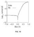
US7943491B2 - Pattern transfer printing by kinetic control of adhesion to an elastomeric stamp - Google Patents
Pattern transfer printing by kinetic control of adhesion to an elastomeric stampDownload PDFInfo
- Publication number
- US7943491B2 US7943491B2US11/423,192US42319206AUS7943491B2US 7943491 B2US7943491 B2US 7943491B2US 42319206 AUS42319206 AUS 42319206AUS 7943491 B2US7943491 B2US 7943491B2
- Authority
- US
- United States
- Prior art keywords
- transfer
- feature
- donor
- separation rate
- substrate
- Prior art date
- Legal status (The legal status is an assumption and is not a legal conclusion. Google has not performed a legal analysis and makes no representation as to the accuracy of the status listed.)
- Active, expires
Links
- 238000010023transfer printingMethods0.000titledescription18
- 238000012546transferMethods0.000claimsabstractdescription407
- 239000000758substrateSubstances0.000claimsabstractdescription243
- 238000000034methodMethods0.000claimsabstractdescription162
- 239000004065semiconductorSubstances0.000claimsabstractdescription153
- 238000000926separation methodMethods0.000claimsdescription191
- 239000010410layerSubstances0.000claimsdescription82
- 239000000463materialSubstances0.000claimsdescription64
- 239000004205dimethyl polysiloxaneSubstances0.000claimsdescription47
- 229920000435poly(dimethylsiloxane)Polymers0.000claimsdescription45
- 229920000642polymerPolymers0.000claimsdescription22
- 229920001971elastomerPolymers0.000claimsdescription19
- 239000000806elastomerSubstances0.000claimsdescription17
- -1polydimethylsiloxanePolymers0.000claimsdescription17
- 238000012545processingMethods0.000claimsdescription16
- 239000011521glassSubstances0.000claimsdescription14
- 239000002086nanomaterialSubstances0.000claimsdescription14
- 238000004519manufacturing processMethods0.000claimsdescription13
- 239000012790adhesive layerSubstances0.000claimsdescription11
- 239000000853adhesiveSubstances0.000claimsdescription9
- 230000001070adhesive effectEffects0.000claimsdescription9
- 229910052751metalInorganic materials0.000claimsdescription8
- 239000002184metalSubstances0.000claimsdescription8
- 239000003989dielectric materialSubstances0.000claimsdescription3
- 229910010293ceramic materialInorganic materials0.000claimsdescription2
- 230000000295complement effectEffects0.000claimsdescription2
- 230000001419dependent effectEffects0.000claimsdescription2
- 239000002105nanoparticleSubstances0.000claimsdescription2
- 239000006187pillSubstances0.000claimsdescription2
- 230000010354integrationEffects0.000abstractdescription16
- 238000003491arrayMethods0.000abstractdescription15
- 230000002153concerted effectEffects0.000abstractdescription3
- XUIMIQQOPSSXEZ-UHFFFAOYSA-NSiliconChemical compound[Si]XUIMIQQOPSSXEZ-UHFFFAOYSA-N0.000description70
- 229910052710siliconInorganic materials0.000description67
- 239000010703siliconSubstances0.000description66
- 235000012431wafersNutrition0.000description35
- 238000007639printingMethods0.000description34
- 230000008569processEffects0.000description28
- VYPSYNLAJGMNEJ-UHFFFAOYSA-NSilicium dioxideChemical compoundO=[Si]=OVYPSYNLAJGMNEJ-UHFFFAOYSA-N0.000description23
- 239000010445micaSubstances0.000description19
- 229910052618mica groupInorganic materials0.000description19
- OKTJSMMVPCPJKN-UHFFFAOYSA-NCarbonChemical compound[C]OKTJSMMVPCPJKN-UHFFFAOYSA-N0.000description14
- 239000000203mixtureSubstances0.000description12
- 229910002804graphiteInorganic materials0.000description11
- 239000010439graphiteSubstances0.000description11
- 238000005096rolling processMethods0.000description11
- 239000007787solidSubstances0.000description11
- JBRZTFJDHDCESZ-UHFFFAOYSA-NAsGaChemical compound[As]#[Ga]JBRZTFJDHDCESZ-UHFFFAOYSA-N0.000description10
- 229910001218Gallium arsenideInorganic materials0.000description10
- 239000000377silicon dioxideSubstances0.000description10
- 239000002019doping agentSubstances0.000description9
- 239000010931goldSubstances0.000description9
- 239000000126substanceSubstances0.000description9
- 229910002601GaNInorganic materials0.000description8
- JMASRVWKEDWRBT-UHFFFAOYSA-NGallium nitrideChemical compound[Ga]#NJMASRVWKEDWRBT-UHFFFAOYSA-N0.000description8
- GPXJNWSHGFTCBW-UHFFFAOYSA-NIndium phosphideChemical compound[In]#PGPXJNWSHGFTCBW-UHFFFAOYSA-N0.000description8
- 239000002131composite materialSubstances0.000description8
- 238000001878scanning electron micrographMethods0.000description8
- 238000013459approachMethods0.000description7
- 230000009286beneficial effectEffects0.000description7
- 229910052681coesiteInorganic materials0.000description7
- 229910052906cristobaliteInorganic materials0.000description7
- 238000000059patterningMethods0.000description7
- 229910052682stishoviteInorganic materials0.000description7
- 229910052905tridymiteInorganic materials0.000description7
- 238000000137annealingMethods0.000description6
- 230000008901benefitEffects0.000description6
- 238000002508contact lithographyMethods0.000description6
- 238000005516engineering processMethods0.000description6
- 229910000831SteelInorganic materials0.000description5
- 238000006073displacement reactionMethods0.000description5
- 238000002474experimental methodMethods0.000description5
- 230000014509gene expressionEffects0.000description5
- 238000012423maintenanceMethods0.000description5
- 239000000123paperSubstances0.000description5
- 229920002120photoresistant polymerPolymers0.000description5
- 239000010959steelSubstances0.000description5
- CPLXHLVBOLITMK-UHFFFAOYSA-NMagnesium oxideChemical compound[Mg]=OCPLXHLVBOLITMK-UHFFFAOYSA-N0.000description4
- 230000032798delaminationEffects0.000description4
- 230000000694effectsEffects0.000description4
- 238000005530etchingMethods0.000description4
- 239000010408filmSubstances0.000description4
- PCHJSUWPFVWCPO-UHFFFAOYSA-NgoldChemical compound[Au]PCHJSUWPFVWCPO-UHFFFAOYSA-N0.000description4
- 229910052737goldInorganic materials0.000description4
- 150000002500ionsChemical class0.000description4
- 230000033001locomotionEffects0.000description4
- 238000012986modificationMethods0.000description4
- 230000004048modificationEffects0.000description4
- 229910021421monocrystalline siliconInorganic materials0.000description4
- 239000000178monomerSubstances0.000description4
- 230000005693optoelectronicsEffects0.000description4
- 238000002174soft lithographyMethods0.000description4
- 229910005542GaSbInorganic materials0.000description3
- 229910000673Indium arsenideInorganic materials0.000description3
- 239000004698PolyethyleneSubstances0.000description3
- 229910007709ZnTeInorganic materials0.000description3
- 239000000919ceramicSubstances0.000description3
- 150000001875compoundsChemical class0.000description3
- 229920001577copolymerPolymers0.000description3
- 230000001747exhibiting effectEffects0.000description3
- 238000009499grossingMethods0.000description3
- 239000012535impuritySubstances0.000description3
- RPQDHPTXJYYUPQ-UHFFFAOYSA-Nindium arsenideChemical compound[In]#[As]RPQDHPTXJYYUPQ-UHFFFAOYSA-N0.000description3
- 239000012212insulatorSubstances0.000description3
- 238000001000micrographMethods0.000description3
- 239000004005microsphereSubstances0.000description3
- 238000000206photolithographyMethods0.000description3
- 238000004987plasma desorption mass spectroscopyMethods0.000description3
- 229920003023plasticPolymers0.000description3
- 239000004033plasticSubstances0.000description3
- 239000004417polycarbonateSubstances0.000description3
- 229920000515polycarbonatePolymers0.000description3
- 229920000573polyethylenePolymers0.000description3
- 229920002635polyurethanePolymers0.000description3
- 239000004814polyurethaneSubstances0.000description3
- 238000003825pressingMethods0.000description3
- SBIBMFFZSBJNJF-UHFFFAOYSA-Nselenium;zincChemical compound[Se]=[Zn]SBIBMFFZSBJNJF-UHFFFAOYSA-N0.000description3
- 229920002725thermoplastic elastomerPolymers0.000description3
- 229910017115AlSbInorganic materials0.000description2
- 229910004613CdTeInorganic materials0.000description2
- 229910005540GaPInorganic materials0.000description2
- 229910002665PbTeInorganic materials0.000description2
- 239000004721Polyphenylene oxideSubstances0.000description2
- 239000004793PolystyreneSubstances0.000description2
- FAPWRFPIFSIZLT-UHFFFAOYSA-MSodium chlorideChemical compound[Na+].[Cl-]FAPWRFPIFSIZLT-UHFFFAOYSA-M0.000description2
- 238000005411Van der Waals forceMethods0.000description2
- 230000006978adaptationEffects0.000description2
- 238000004458analytical methodMethods0.000description2
- 239000012620biological materialSubstances0.000description2
- UHYPYGJEEGLRJD-UHFFFAOYSA-Ncadmium(2+);selenium(2-)Chemical compound[Se-2].[Cd+2]UHYPYGJEEGLRJD-UHFFFAOYSA-N0.000description2
- 238000005266castingMethods0.000description2
- 238000000576coating methodMethods0.000description2
- 239000013078crystalSubstances0.000description2
- 230000007423decreaseEffects0.000description2
- 230000003247decreasing effectEffects0.000description2
- 238000000151depositionMethods0.000description2
- YGANSGVIUGARFR-UHFFFAOYSA-Ndipotassium dioxosilane oxo(oxoalumanyloxy)alumane oxygen(2-)Chemical compound[O--].[K+].[K+].O=[Si]=O.O=[Al]O[Al]=OYGANSGVIUGARFR-UHFFFAOYSA-N0.000description2
- 238000009826distributionMethods0.000description2
- 239000013536elastomeric materialSubstances0.000description2
- 230000008570general processEffects0.000description2
- 229910052732germaniumInorganic materials0.000description2
- 229910021389grapheneInorganic materials0.000description2
- 229910001385heavy metalInorganic materials0.000description2
- 238000010348incorporationMethods0.000description2
- WPYVAWXEWQSOGY-UHFFFAOYSA-Nindium antimonideChemical compound[Sb]#[In]WPYVAWXEWQSOGY-UHFFFAOYSA-N0.000description2
- 238000009616inductively coupled plasmaMethods0.000description2
- 230000003993interactionEffects0.000description2
- 239000000395magnesium oxideSubstances0.000description2
- 150000002739metalsChemical class0.000description2
- 229910052627muscoviteInorganic materials0.000description2
- 229920000620organic polymerPolymers0.000description2
- 229920002223polystyrenePolymers0.000description2
- 238000002360preparation methodMethods0.000description2
- 229920005989resinPolymers0.000description2
- 239000011347resinSubstances0.000description2
- 238000010020roller printingMethods0.000description2
- 239000005060rubberSubstances0.000description2
- 239000000523sampleSubstances0.000description2
- 238000001338self-assemblyMethods0.000description2
- 230000003746surface roughnessEffects0.000description2
- OCGWQDWYSQAFTO-UHFFFAOYSA-NtellanylideneleadChemical compound[Pb]=[Te]OCGWQDWYSQAFTO-UHFFFAOYSA-N0.000description2
- 239000010409thin filmSubstances0.000description2
- XLYOFNOQVPJJNP-UHFFFAOYSA-NwaterSubstancesOXLYOFNOQVPJJNP-UHFFFAOYSA-N0.000description2
- 238000003466weldingMethods0.000description2
- YBNMDCCMCLUHBL-UHFFFAOYSA-N(2,5-dioxopyrrolidin-1-yl) 4-pyren-1-ylbutanoateChemical compoundC=1C=C(C2=C34)C=CC3=CC=CC4=CC=C2C=1CCCC(=O)ON1C(=O)CCC1=OYBNMDCCMCLUHBL-UHFFFAOYSA-N0.000description1
- 108091032973(ribonucleotides)n+mProteins0.000description1
- 229910000980Aluminium gallium arsenideInorganic materials0.000description1
- 229910015844BCl3Inorganic materials0.000description1
- OYPRJOBELJOOCE-UHFFFAOYSA-NCalciumChemical compound[Ca]OYPRJOBELJOOCE-UHFFFAOYSA-N0.000description1
- RYGMFSIKBFXOCR-UHFFFAOYSA-NCopperChemical compound[Cu]RYGMFSIKBFXOCR-UHFFFAOYSA-N0.000description1
- 229910021591Copper(I) chlorideInorganic materials0.000description1
- 108020004414DNAProteins0.000description1
- 229910005543GaSeInorganic materials0.000description1
- 229910000530Gallium indium arsenideInorganic materials0.000description1
- 101000651211Homo sapiens Transcription factor PU.1Proteins0.000description1
- DGAQECJNVWCQMB-PUAWFVPOSA-MIlexoside XXIXChemical compoundC[C@@H]1CC[C@@]2(CC[C@@]3(C(=CC[C@H]4[C@]3(CC[C@@H]5[C@@]4(CC[C@@H](C5(C)C)OS(=O)(=O)[O-])C)C)[C@@H]2[C@]1(C)O)C)C(=O)O[C@H]6[C@@H]([C@H]([C@@H]([C@H](O6)CO)O)O)O.[Na+]DGAQECJNVWCQMB-PUAWFVPOSA-M0.000description1
- VVQNEPGJFQJSBK-UHFFFAOYSA-NMethyl methacrylateChemical compoundCOC(=O)C(C)=CVVQNEPGJFQJSBK-UHFFFAOYSA-N0.000description1
- 229920001890NovodurPolymers0.000description1
- CBENFWSGALASAD-UHFFFAOYSA-NOzoneChemical compound[O-][O+]=OCBENFWSGALASAD-UHFFFAOYSA-N0.000description1
- 239000004952PolyamideSubstances0.000description1
- 239000004962Polyamide-imideSubstances0.000description1
- 239000004693PolybenzimidazoleSubstances0.000description1
- 239000005062PolybutadieneSubstances0.000description1
- 239000004697PolyetherimideSubstances0.000description1
- 239000004642PolyimideSubstances0.000description1
- 229920002367PolyisobutenePolymers0.000description1
- 239000004734Polyphenylene sulfideSubstances0.000description1
- 239000004954PolyphthalamideSubstances0.000description1
- 239000004743PolypropyleneSubstances0.000description1
- 101000836070Rattus norvegicus Serine protease inhibitor A3LProteins0.000description1
- 229910000577Silicon-germaniumInorganic materials0.000description1
- 241001671243Streptocarpus ionanthusSpecies0.000description1
- 102100027654Transcription factor PU.1Human genes0.000description1
- XLOMVQKBTHCTTD-UHFFFAOYSA-NZinc monoxideChemical compound[Zn]=OXLOMVQKBTHCTTD-UHFFFAOYSA-N0.000description1
- 150000001252acrylic acid derivativesChemical class0.000description1
- 230000004913activationEffects0.000description1
- 239000000654additiveSubstances0.000description1
- 230000000996additive effectEffects0.000description1
- 229910045601alloyInorganic materials0.000description1
- 239000000956alloySubstances0.000description1
- 230000000181anti-adherent effectEffects0.000description1
- 239000007900aqueous suspensionSubstances0.000description1
- 238000003556assayMethods0.000description1
- 230000000712assemblyEffects0.000description1
- 238000000429assemblyMethods0.000description1
- 238000004630atomic force microscopyMethods0.000description1
- QVGXLLKOCUKJST-UHFFFAOYSA-Natomic oxygenChemical compound[O]QVGXLLKOCUKJST-UHFFFAOYSA-N0.000description1
- 229920002988biodegradable polymerPolymers0.000description1
- 239000004621biodegradable polymerSubstances0.000description1
- 229960000074biopharmaceuticalDrugs0.000description1
- 229910052791calciumInorganic materials0.000description1
- 239000011575calciumSubstances0.000description1
- 229910052799carbonInorganic materials0.000description1
- 230000015556catabolic processEffects0.000description1
- 230000008859changeEffects0.000description1
- 125000003636chemical groupChemical group0.000description1
- 238000007385chemical modificationMethods0.000description1
- 239000003153chemical reaction reagentSubstances0.000description1
- 238000011109contaminationMethods0.000description1
- 229910052802copperInorganic materials0.000description1
- 239000010949copperSubstances0.000description1
- OXBLHERUFWYNTN-UHFFFAOYSA-Mcopper(I) chlorideChemical compound[Cu]ClOXBLHERUFWYNTN-UHFFFAOYSA-M0.000description1
- BERDEBHAJNAUOM-UHFFFAOYSA-Ncopper(I) oxideInorganic materials[Cu]O[Cu]BERDEBHAJNAUOM-UHFFFAOYSA-N0.000description1
- 238000005336crackingMethods0.000description1
- 229920006037cross link polymerPolymers0.000description1
- 239000002178crystalline materialSubstances0.000description1
- KRFJLUBVMFXRPN-UHFFFAOYSA-Ncuprous oxideChemical compound[O-2].[Cu+].[Cu+]KRFJLUBVMFXRPN-UHFFFAOYSA-N0.000description1
- 230000007547defectEffects0.000description1
- 238000006731degradation reactionMethods0.000description1
- 239000008367deionised waterSubstances0.000description1
- 229910021641deionized waterInorganic materials0.000description1
- 230000008021depositionEffects0.000description1
- 238000013461designMethods0.000description1
- 238000001514detection methodMethods0.000description1
- 238000011161developmentMethods0.000description1
- 229910003460diamondInorganic materials0.000description1
- 239000010432diamondSubstances0.000description1
- 238000002408directed self-assemblyMethods0.000description1
- 238000001035dryingMethods0.000description1
- 230000005489elastic deformationEffects0.000description1
- 238000005566electron beam evaporationMethods0.000description1
- 238000010894electron beam technologyMethods0.000description1
- 238000004146energy storageMethods0.000description1
- 229920002457flexible plasticPolymers0.000description1
- 239000012530fluidSubstances0.000description1
- 229920002313fluoropolymerPolymers0.000description1
- 239000004811fluoropolymerSubstances0.000description1
- 239000006260foamSubstances0.000description1
- 238000009472formulationMethods0.000description1
- GNPVGFCGXDBREM-UHFFFAOYSA-Ngermanium atomChemical compound[Ge]GNPVGFCGXDBREM-UHFFFAOYSA-N0.000description1
- 230000005484gravityEffects0.000description1
- 229910052739hydrogenInorganic materials0.000description1
- 239000001257hydrogenSubstances0.000description1
- 230000005660hydrophilic surfaceEffects0.000description1
- 230000002209hydrophobic effectEffects0.000description1
- 230000005661hydrophobic surfaceEffects0.000description1
- 125000002887hydroxy groupChemical group[H]O*0.000description1
- 238000005286illuminationMethods0.000description1
- 238000003384imaging methodMethods0.000description1
- 239000004615ingredientSubstances0.000description1
- 229920000592inorganic polymerPolymers0.000description1
- 239000007788liquidSubstances0.000description1
- 229910001092metal group alloyInorganic materials0.000description1
- 238000001465metallisationMethods0.000description1
- 230000002906microbiologic effectEffects0.000description1
- 238000004377microelectronicMethods0.000description1
- 238000005459micromachiningMethods0.000description1
- 229910003465moissaniteInorganic materials0.000description1
- 229910052961molybdeniteInorganic materials0.000description1
- CWQXQMHSOZUFJS-UHFFFAOYSA-Nmolybdenum disulfideChemical compoundS=[Mo]=SCWQXQMHSOZUFJS-UHFFFAOYSA-N0.000description1
- 229910052982molybdenum disulfideInorganic materials0.000description1
- 230000000926neurological effectEffects0.000description1
- 150000004767nitridesChemical class0.000description1
- 229910052757nitrogenInorganic materials0.000description1
- 229920001778nylonPolymers0.000description1
- 230000003287optical effectEffects0.000description1
- 239000013307optical fiberSubstances0.000description1
- 238000000879optical micrographMethods0.000description1
- 229910052760oxygenInorganic materials0.000description1
- 239000001301oxygenSubstances0.000description1
- 239000003973paintSubstances0.000description1
- 239000002245particleSubstances0.000description1
- 230000037361pathwayEffects0.000description1
- 230000000737periodic effectEffects0.000description1
- 230000010363phase shiftEffects0.000description1
- 229910052698phosphorusInorganic materials0.000description1
- 230000000704physical effectEffects0.000description1
- 238000001020plasma etchingMethods0.000description1
- 238000000623plasma-assisted chemical vapour depositionMethods0.000description1
- 229920001084poly(chloroprene)Polymers0.000description1
- 229920003223poly(pyromellitimide-1,4-diphenyl ether)Polymers0.000description1
- 229920002239polyacrylonitrilePolymers0.000description1
- 229920002647polyamidePolymers0.000description1
- 229920002312polyamide-imidePolymers0.000description1
- 229920001230polyarylatePolymers0.000description1
- 229920002480polybenzimidazolePolymers0.000description1
- 229920002857polybutadienePolymers0.000description1
- 229920001748polybutylenePolymers0.000description1
- 229910021420polycrystalline siliconInorganic materials0.000description1
- 229920000728polyesterPolymers0.000description1
- 229920000570polyetherPolymers0.000description1
- 229920001601polyetherimidePolymers0.000description1
- 229920001721polyimidePolymers0.000description1
- 229920001470polyketonePolymers0.000description1
- 229920000306polymethylpentenePolymers0.000description1
- 239000011116polymethylpenteneSubstances0.000description1
- 229920000098polyolefinPolymers0.000description1
- 229920006324polyoxymethylenePolymers0.000description1
- 229920001184polypeptidePolymers0.000description1
- 229920006380polyphenylene oxidePolymers0.000description1
- 229920000069polyphenylene sulfidePolymers0.000description1
- 229920006375polyphtalamidePolymers0.000description1
- 229920001155polypropylenePolymers0.000description1
- 229920001296polysiloxanePolymers0.000description1
- 229910021426porous siliconInorganic materials0.000description1
- 238000005381potential energyMethods0.000description1
- 108090000765processed proteins & peptidesProteins0.000description1
- 102000004196processed proteins & peptidesHuman genes0.000description1
- 108090000623proteins and genesProteins0.000description1
- 102000004169proteins and genesHuman genes0.000description1
- 238000000746purificationMethods0.000description1
- 238000011160researchMethods0.000description1
- 230000004044responseEffects0.000description1
- 230000002441reversible effectEffects0.000description1
- 229910010271silicon carbideInorganic materials0.000description1
- 235000012239silicon dioxideNutrition0.000description1
- 229910052814silicon oxideInorganic materials0.000description1
- 229910052708sodiumInorganic materials0.000description1
- 239000011734sodiumSubstances0.000description1
- 239000011780sodium chlorideSubstances0.000description1
- 125000006850spacer groupChemical group0.000description1
- 239000007858starting materialSubstances0.000description1
- 230000003068static effectEffects0.000description1
- 125000001174sulfone groupChemical group0.000description1
- 239000000725suspensionSubstances0.000description1
- 229920003051synthetic elastomerPolymers0.000description1
- 238000010189synthetic methodMethods0.000description1
- 239000005061synthetic rubberSubstances0.000description1
- 238000012360testing methodMethods0.000description1
- 229920001169thermoplasticPolymers0.000description1
- 239000004416thermosoftening plasticSubstances0.000description1
- 229910052723transition metalInorganic materials0.000description1
- PISDRBMXQBSCIP-UHFFFAOYSA-Ntrichloro(3,3,4,4,5,5,6,6,7,7,8,8,8-tridecafluorooctyl)silaneChemical compoundFC(F)(F)C(F)(F)C(F)(F)C(F)(F)C(F)(F)C(F)(F)CC[Si](Cl)(Cl)ClPISDRBMXQBSCIP-UHFFFAOYSA-N0.000description1
- FAQYAMRNWDIXMY-UHFFFAOYSA-NtrichloroboraneChemical compoundClB(Cl)ClFAQYAMRNWDIXMY-UHFFFAOYSA-N0.000description1
- 238000009827uniform distributionMethods0.000description1
- 125000000391vinyl groupChemical group[H]C([*])=C([H])[H]0.000description1
- 229920002554vinyl polymerPolymers0.000description1
Images


Classifications
- H—ELECTRICITY
- H10—SEMICONDUCTOR DEVICES; ELECTRIC SOLID-STATE DEVICES NOT OTHERWISE PROVIDED FOR
- H10D—INORGANIC ELECTRIC SEMICONDUCTOR DEVICES
- H10D62/00—Semiconductor bodies, or regions thereof, of devices having potential barriers
- H10D62/10—Shapes, relative sizes or dispositions of the regions of the semiconductor bodies; Shapes of the semiconductor bodies
- H10D62/117—Shapes of semiconductor bodies
- H10D62/118—Nanostructure semiconductor bodies
- B—PERFORMING OPERATIONS; TRANSPORTING
- B82—NANOTECHNOLOGY
- B82Y—SPECIFIC USES OR APPLICATIONS OF NANOSTRUCTURES; MEASUREMENT OR ANALYSIS OF NANOSTRUCTURES; MANUFACTURE OR TREATMENT OF NANOSTRUCTURES
- B82Y10/00—Nanotechnology for information processing, storage or transmission, e.g. quantum computing or single electron logic
- H—ELECTRICITY
- H10—SEMICONDUCTOR DEVICES; ELECTRIC SOLID-STATE DEVICES NOT OTHERWISE PROVIDED FOR
- H10D—INORGANIC ELECTRIC SEMICONDUCTOR DEVICES
- H10D62/00—Semiconductor bodies, or regions thereof, of devices having potential barriers
- H10D62/10—Shapes, relative sizes or dispositions of the regions of the semiconductor bodies; Shapes of the semiconductor bodies
- H10D62/117—Shapes of semiconductor bodies
- H10D62/118—Nanostructure semiconductor bodies
- H10D62/119—Nanowire, nanosheet or nanotube semiconductor bodies
- H10D62/121—Nanowire, nanosheet or nanotube semiconductor bodies oriented parallel to substrates
- H—ELECTRICITY
- H10—SEMICONDUCTOR DEVICES; ELECTRIC SOLID-STATE DEVICES NOT OTHERWISE PROVIDED FOR
- H10D—INORGANIC ELECTRIC SEMICONDUCTOR DEVICES
- H10D62/00—Semiconductor bodies, or regions thereof, of devices having potential barriers
- H10D62/80—Semiconductor bodies, or regions thereof, of devices having potential barriers characterised by the materials
- H10D62/881—Semiconductor bodies, or regions thereof, of devices having potential barriers characterised by the materials being a two-dimensional material
- H10D62/882—Graphene
- H—ELECTRICITY
- H10—SEMICONDUCTOR DEVICES; ELECTRIC SOLID-STATE DEVICES NOT OTHERWISE PROVIDED FOR
- H10F—INORGANIC SEMICONDUCTOR DEVICES SENSITIVE TO INFRARED RADIATION, LIGHT, ELECTROMAGNETIC RADIATION OF SHORTER WAVELENGTH OR CORPUSCULAR RADIATION
- H10F10/00—Individual photovoltaic cells, e.g. solar cells
- H10F10/10—Individual photovoltaic cells, e.g. solar cells having potential barriers
- H10F10/16—Photovoltaic cells having only PN heterojunction potential barriers
- H—ELECTRICITY
- H10—SEMICONDUCTOR DEVICES; ELECTRIC SOLID-STATE DEVICES NOT OTHERWISE PROVIDED FOR
- H10F—INORGANIC SEMICONDUCTOR DEVICES SENSITIVE TO INFRARED RADIATION, LIGHT, ELECTROMAGNETIC RADIATION OF SHORTER WAVELENGTH OR CORPUSCULAR RADIATION
- H10F30/00—Individual radiation-sensitive semiconductor devices in which radiation controls the flow of current through the devices, e.g. photodetectors
- H10F30/20—Individual radiation-sensitive semiconductor devices in which radiation controls the flow of current through the devices, e.g. photodetectors the devices having potential barriers, e.g. phototransistors
- H10F30/21—Individual radiation-sensitive semiconductor devices in which radiation controls the flow of current through the devices, e.g. photodetectors the devices having potential barriers, e.g. phototransistors the devices being sensitive to infrared, visible or ultraviolet radiation
- H10F30/22—Individual radiation-sensitive semiconductor devices in which radiation controls the flow of current through the devices, e.g. photodetectors the devices having potential barriers, e.g. phototransistors the devices being sensitive to infrared, visible or ultraviolet radiation the devices having only one potential barrier, e.g. photodiodes
- H10F30/222—Individual radiation-sensitive semiconductor devices in which radiation controls the flow of current through the devices, e.g. photodetectors the devices having potential barriers, e.g. phototransistors the devices being sensitive to infrared, visible or ultraviolet radiation the devices having only one potential barrier, e.g. photodiodes the potential barrier being a PN heterojunction
- H—ELECTRICITY
- H10—SEMICONDUCTOR DEVICES; ELECTRIC SOLID-STATE DEVICES NOT OTHERWISE PROVIDED FOR
- H10F—INORGANIC SEMICONDUCTOR DEVICES SENSITIVE TO INFRARED RADIATION, LIGHT, ELECTROMAGNETIC RADIATION OF SHORTER WAVELENGTH OR CORPUSCULAR RADIATION
- H10F71/00—Manufacture or treatment of devices covered by this subclass
- H10F71/121—The active layers comprising only Group IV materials
- H—ELECTRICITY
- H10—SEMICONDUCTOR DEVICES; ELECTRIC SOLID-STATE DEVICES NOT OTHERWISE PROVIDED FOR
- H10F—INORGANIC SEMICONDUCTOR DEVICES SENSITIVE TO INFRARED RADIATION, LIGHT, ELECTROMAGNETIC RADIATION OF SHORTER WAVELENGTH OR CORPUSCULAR RADIATION
- H10F71/00—Manufacture or treatment of devices covered by this subclass
- H10F71/139—Manufacture or treatment of devices covered by this subclass using temporary substrates
- H—ELECTRICITY
- H10—SEMICONDUCTOR DEVICES; ELECTRIC SOLID-STATE DEVICES NOT OTHERWISE PROVIDED FOR
- H10F—INORGANIC SEMICONDUCTOR DEVICES SENSITIVE TO INFRARED RADIATION, LIGHT, ELECTROMAGNETIC RADIATION OF SHORTER WAVELENGTH OR CORPUSCULAR RADIATION
- H10F77/00—Constructional details of devices covered by this subclass
- H10F77/10—Semiconductor bodies
- H10F77/14—Shape of semiconductor bodies; Shapes, relative sizes or dispositions of semiconductor regions within semiconductor bodies
- H10F77/147—Shapes of bodies
- H—ELECTRICITY
- H10—SEMICONDUCTOR DEVICES; ELECTRIC SOLID-STATE DEVICES NOT OTHERWISE PROVIDED FOR
- H10F—INORGANIC SEMICONDUCTOR DEVICES SENSITIVE TO INFRARED RADIATION, LIGHT, ELECTROMAGNETIC RADIATION OF SHORTER WAVELENGTH OR CORPUSCULAR RADIATION
- H10F77/00—Constructional details of devices covered by this subclass
- H10F77/10—Semiconductor bodies
- H10F77/16—Material structures, e.g. crystalline structures, film structures or crystal plane orientations
- H10F77/169—Thin semiconductor films on metallic or insulating substrates
- H10F77/1696—Thin semiconductor films on metallic or insulating substrates the films including Group II-VI materials, e.g. CdTe or CdS
- B—PERFORMING OPERATIONS; TRANSPORTING
- B82—NANOTECHNOLOGY
- B82Y—SPECIFIC USES OR APPLICATIONS OF NANOSTRUCTURES; MEASUREMENT OR ANALYSIS OF NANOSTRUCTURES; MANUFACTURE OR TREATMENT OF NANOSTRUCTURES
- B82Y20/00—Nanooptics, e.g. quantum optics or photonic crystals
- H—ELECTRICITY
- H01—ELECTRIC ELEMENTS
- H01L—SEMICONDUCTOR DEVICES NOT COVERED BY CLASS H10
- H01L2924/00—Indexing scheme for arrangements or methods for connecting or disconnecting semiconductor or solid-state bodies as covered by H01L24/00
- H01L2924/10—Details of semiconductor or other solid state devices to be connected
- H01L2924/11—Device type
- H01L2924/12—Passive devices, e.g. 2 terminal devices
- H01L2924/1204—Optical Diode
- H01L2924/12041—LED
- H—ELECTRICITY
- H01—ELECTRIC ELEMENTS
- H01L—SEMICONDUCTOR DEVICES NOT COVERED BY CLASS H10
- H01L2924/00—Indexing scheme for arrangements or methods for connecting or disconnecting semiconductor or solid-state bodies as covered by H01L24/00
- H01L2924/10—Details of semiconductor or other solid state devices to be connected
- H01L2924/11—Device type
- H01L2924/13—Discrete devices, e.g. 3 terminal devices
- H01L2924/1304—Transistor
- H01L2924/1306—Field-effect transistor [FET]
- H01L2924/13091—Metal-Oxide-Semiconductor Field-Effect Transistor [MOSFET]
- H—ELECTRICITY
- H10—SEMICONDUCTOR DEVICES; ELECTRIC SOLID-STATE DEVICES NOT OTHERWISE PROVIDED FOR
- H10D—INORGANIC ELECTRIC SEMICONDUCTOR DEVICES
- H10D30/00—Field-effect transistors [FET]
- H10D30/60—Insulated-gate field-effect transistors [IGFET]
- H10D30/67—Thin-film transistors [TFT]
- H10D30/6758—Thin-film transistors [TFT] characterised by the insulating substrates
- Y—GENERAL TAGGING OF NEW TECHNOLOGICAL DEVELOPMENTS; GENERAL TAGGING OF CROSS-SECTIONAL TECHNOLOGIES SPANNING OVER SEVERAL SECTIONS OF THE IPC; TECHNICAL SUBJECTS COVERED BY FORMER USPC CROSS-REFERENCE ART COLLECTIONS [XRACs] AND DIGESTS
- Y02—TECHNOLOGIES OR APPLICATIONS FOR MITIGATION OR ADAPTATION AGAINST CLIMATE CHANGE
- Y02E—REDUCTION OF GREENHOUSE GAS [GHG] EMISSIONS, RELATED TO ENERGY GENERATION, TRANSMISSION OR DISTRIBUTION
- Y02E10/00—Energy generation through renewable energy sources
- Y02E10/50—Photovoltaic [PV] energy
- Y02E10/547—Monocrystalline silicon PV cells
- Y—GENERAL TAGGING OF NEW TECHNOLOGICAL DEVELOPMENTS; GENERAL TAGGING OF CROSS-SECTIONAL TECHNOLOGIES SPANNING OVER SEVERAL SECTIONS OF THE IPC; TECHNICAL SUBJECTS COVERED BY FORMER USPC CROSS-REFERENCE ART COLLECTIONS [XRACs] AND DIGESTS
- Y02—TECHNOLOGIES OR APPLICATIONS FOR MITIGATION OR ADAPTATION AGAINST CLIMATE CHANGE
- Y02P—CLIMATE CHANGE MITIGATION TECHNOLOGIES IN THE PRODUCTION OR PROCESSING OF GOODS
- Y02P70/00—Climate change mitigation technologies in the production process for final industrial or consumer products
- Y02P70/50—Manufacturing or production processes characterised by the final manufactured product
Definitions
- the present inventionencompasses a deterministic, high-speed approach for manipulation and heterogeneous integration that uses kinetically controlled adhesion to elastomeric transfer devices, or stamps, to transfer print solid objects from one substrate to another.
- This techniqueprovides an important combination of capabilities that is not offered by other assembly methods, such as those based on ‘pick and place’ technologies, wafer bonding, or directed self-assembly.
- the method presented hereinallows manipulation of arrays of objects based on kinetically controllable adhesion to a viscoelastic stamp in a massively parallel and deterministic manner.
- the mechanicssuggest paths for optimizing the material properties of the stamps in ways that have not been explored in soft lithography or related areas.
- the printing procedureprovides robust capabilities for generating microstructured hybrid materials systems and device arrays with applications in optoelectronics, photonics, non-planar fabrication and biotechnology without the use of precision moving parts, applied electric or magnetic fields.
- the stamp-based methods of the present inventionare invaluable tools for handling the building blocks of nano- and other emerging technologies to construct devices based on these technologies.
- the present inventionprovides methods, systems and system components for transferring, assembling and integrating features and arrays of features having selected nanosized and/or microsized physical dimensions, shapes and spatial orientations.
- Methods of the present inventionutilize principles of ‘soft adhesion’ to guide the transfer, assembly and/or integration of features, such as printable semiconductor elements or other components of electronic devices.
- Methods of the present inventionare useful for transferring features from a donor substrate to the transfer surface of an elastomeric transfer device and, optionally, from the transfer surface of an elastomeric transfer device to the receiving surface of a receiving substrate.
- the present methods and systemsprovide highly efficient, registered transfer of features and arrays of features, such as printable semiconductor elements, in a concerted manner that maintains the relative spatial orientations of transferred features.
- the present methods and systemsexploit the viscoelastic properties of elastomeric transfer devices to provide kinetic control of adhesion between a transfer surface of the transfer device and features subject to processing via transfer, assembly or integration.
- the viscoelastic nature of the elastomeric material of the transfer deviceresults in an adhesion force that depends, at least in part, on the rate that the transfer surface is peeled away or otherwise separated from a donor substrate having features disposed thereon, or the rate that the transfer surface having features disposed thereon is peeled away or otherwise separated from a receiving substrate.
- High separation ratesare used in the present invention, for example, to generate adhesion forces large enough to transfer features, such as printable semiconductor elements, from a donor substrate to a transfer surface of an elastomeric transfer device.
- Low separation ratesare used in the present invention, for example, to generate adhesion forces low enough to facilitate transfer of features, such as printable semiconductor elements, disposed on a transfer surface of an elastomeric transfer device to a donor substrate.
- Methods of this aspect of the present inventionare useful for transferring, assembling and integrating a wide range of useful materials and structures, device components and/or functional devices onto or into a receiving substrate with high placement accuracy and pattern fidelity, particularly in the context of transfer contact printing.
- the methods and systems of the present inventionare compatible with a range of receiving substrate compositions including polymer, ceramic, metal, semiconductor, paper, and glass substrates, substrate geometries including planar and contoured substrates, and substrate surface morphologies including smooth and rough substrates.
- the inventionis particularly useful for generating patterns of features on surfaces of substrates exhibiting excellent reproducibility, pattern fidelity and resolution.
- the present inventionis capable of high throughput patterning of large receiving substrate areas (greater than or equal to about 232 cm 2 ) and, thus, enable a robust and commercially attractive manufacturing pathway to a range of functional systems and devices including electronic device arrays, nano- and micro-electromechanical systems, nano and micro-biological systems, sensors, energy storage devices and integrated electronic circuits.
- nanopatterning and micropatterning methods and systems of the present inventionare compatible with a wide range of substrates and materials, including semiconductors, wafers, metals, metal alloys, semimetals, insulators, crystalline materials, amorphous materials, biological materials, and the methods can be employed under a wide range of processing conditions, including low temperature ( ⁇ about 400 degrees Celsius) processing.
- the present inventionprovides methods for transferring features, including nanosized and/or microsized structures, using an elastomeric transfer device to transfer a feature from a first substrate surface to a second substrate surface by applying different kinetic separation (e.g., using a different peeling rate and/or separation rate for example) of surfaces to variably control adhesion of the feature to the transfer surface of an elastomeric transfer device.
- different kinetic separatione.g., using a different peeling rate and/or separation rate for example
- the inventionprovides a method of transferring a feature from a donor substrate surface to a receiving substrate surface, optionally providing registered transfer of features and feature arrays from the donor substrate to the receiving substrate.
- a method of this aspect of the present inventioncomprises the step of providing an elastomeric transfer device having a transfer surface and providing a donor substrate having a donor surface.
- the donor surfacehas at least one feature disposed thereon.
- the methodfurther comprises the step of contacting at least a portion of the transfer surface with at least a portion of the donor surface feature and physically separating the transfer surface from the donor surface at a first separation rate such that at least a portion of the feature is transferred from the donor surface to the transfer surface.
- the methodfurther comprises the step of providing a receiving substrate having a receiving surface, and contacting at least a portion of the feature disposed on the transfer surface with the receiving surface.
- the transfer surface having features disposed thereonis separated from the receiving surface at a second separation rate, that is less than the first separation rate, such that at least a portion of the feature disposed on the transfer surface is transferred to the receiving surface, thereby transferring a feature from the donor surface to the receiving surface.
- a first separation rate greater than the second separationis beneficial for providing efficient transfer from the donor substrate to the receiving substrate.
- separation rateand peel rate” are used synonymously in the present description.
- a “feature”refers to a structure on, or an integral part of, a donor surface to be transferred to an elastomeric transfer device and/or a receiving surface of a receiving substrate.
- the term featureencompasses a free-standing structure supported by a donor surface, such as an entirely undercut free-standing structure and encompasses a feature that is integral connected to the donor surface (e.g., a monolithic structure, or discrete structures connected by an adhesive layer or by surface forces including van der Waals forces, etc.), such as a completely or partially undercut structure connected to the donor surface via one or more bridge elements and/or other alignment maintenance elements.
- featurecomprises one or more printable semiconductor elements, patterns of printable semiconductor elements and arrays of printable semiconductor elements.
- a featurealso refers to a pattern or an array of structures, and encompasses patterns of nanostructures, patterns of microstructures or a pattern of microstructures and nanostructures.
- a featurecomprises a functional device component or functional device.
- the viscoelastic properties of an elastomeric transfer deviceenables precise control of adhesion forces involved in transfer of features from a donor substrate to a transfer surface of a transfer device and from the transfer surface of a transfer device to a receiving substrate.
- Elastomeric transfer devices of the present inventionmay comprise any elastomer material, including composite materials, so long as the transfer device exhibits viscoelastic behavior such that adhesion between a feature and the transfer device is rate-sensitive. Accordingly, selection of the composition, physical dimensions (e.g. thickness) and mechanical properties of the elastomeric transfer device used in the present methods is important to provide high yield transfer efficiencies, and optionally registered transfer.
- the elastomeric transfer devicecomprises at least one elastomer layer having a Young's modulus between about 1 MPa and about 20 MPa. In an embodiment, the elastomeric transfer device comprises at least one elastomer layer having a thickness between about 1 micron and about 100 microns. In an embodiment, the elastomeric transfer device comprises an elastomeric stamp, elastomeric mold or elastomeric photomask. In one embodiment, the elastomeric transfer device comprises polydimethylsiloxane. In another embodiment, the transfer device comprises perfluorinated polyether. In another embodiment, the transfer device comprises Scotch® tape.
- an elastomeric transfer deviceis also beneficial in the present methods because it is capable of providing conformal contact with the surfaces of features, donor substrates and/or receiving substrates.
- conformal contactis established between the transfer surface of the elastomeric transfer device and an external surface of the feature and optionally, conformal contact is established between the transfer surface having the feature disposed thereon and the receiving surface of the receiving substrate.
- the term “external surface”refers to a feature surface that is accessible to the transfer surface.
- the rate that the elastomeric transfer device is separated from substrates and/or features on substratesis selected so as to generate adhesive forces useful for transferring, assembling and integrating features.
- the first separation rateis at least 10 times larger than the second separation rate, and in some embodiments the first separation rate is at least 100 times larger than the second separation rate.
- the first separation rateis greater than or equal to about 10 cm/s so as to provide efficient transfer of one or more features from the surface of a donor substrate to the transfer surface of the transfer device and the second separation rate is less than or equal to about 1 mm/s so as to provide efficient transfer of one or more features from the transfer surface of the transfer device to the receiving surface of a receiving substrate.
- features undergoing transferhave lengths selected over the range of about 100 nanometers to about 1000 microns, widths selected over the range of about 100 nanometers to about 1000 microns and thicknesses selected over the range of about 1 nanometer to about 1000 microns, and the first separation rate is selected over the range of about 100 cm/s to 0.1 mm/s and/or the second separation rate is selected over the range of about 0.1 mm/s to 100 cm/s.
- the first separation rateselected so as to generate a separation energy between the feature and the transfer surface of the elastomeric transfer device per unit area equal to or greater than 4 J/m 2 .
- Separation rates useful in the present inventionmay be constant, substantially constant, or variable with respect to time.
- the expression “substantially constant with respect to time”refers to a separation rate that varies by less than 10% over a separation time (or peel time) interval.
- a separation rate that is “substantially constant”refers to a separation rate that varies less than 10% over a separation time interval and/or less than 10% over a separation region.
- the inventionoptionally further comprises use of a first separation rate, a second separation rate or both first and second separation rates that are substantially constant as a function of time.
- the first separation rate, the second separation rate or both the first and second separation ratevaries selectively as a function of time, for example increasing, decreasing, or having an interval or region over which the rate increases and a second interval or region over which the rate decreases as separation proceeds across distance or time.
- the present inventionincludes methods wherein the feature is connected to the donor surface, for example by one or more bridge elements or other alignment maintenance elements, and the first separation rate is large enough so as to cause release of the feature from the donor surface.
- the featureis connected to the donor surface via at least one bridge element and the first separation rate is large enough to cause fracture of the bridge element(s), thereby resulting in release of the feature from the donor surface.
- the present inventionincludes methods wherein the feature is a free standing structure supported by the donor surface, wherein the first separation rate is large enough to release the structure from the donor surface onto the transfer surface of the transfer element.
- the inventionprovides methods wherein the steps of: contacting at least a portion of the transfer surface with at least a portion of the feature; separating the transfer surface from the donor surface at the first separation rate; contacting at least a portion of the feature disposed on the transfer surface with the receiving surface of the receiving substrate; separating the transfer surface from the feature at a second separation rate or any combination of these steps are carried out via an actuator, such as a roller printing or flexographic printing assembly or a mechanical stage, operationally connected to the transfer device.
- an actuatorsuch as a roller printing or flexographic printing assembly or a mechanical stage
- the inventionfurther comprises the steps of: providing a plurality of printable semiconductor elements wherein each of the printable semiconductor element is optionally connected to the donor substrate via at least one bridge element; the method further comprising the steps of: contacting at least a portion of the transfer surface with at least a portion of the pattern of printable semiconductor element; separating the transfer surface from the donor surface at a first separation rate such that at least a portion of the bridge elements are fractured and at least a portion of the pattern of printable semiconductor elements is transferred from the donor surface to the transfer surface, thereby forming the transfer surface having the printable semiconductor elements disposed thereon; contacting at least a portion of the printable semiconductor elements disposed on the transfer surface with the receiving surface of the receiving substrate; and separating the transfer surface from the feature at a second separation rate, wherein the first separation rate is larger than the second separation rate, thereby transferring at least a portion of the pattern of printable semiconductor elements to the receiving surface.
- the printable semiconductor elementis connected to the donor substrate via one or more bridge elements (or other alignment maintenance elements), wherein the separation rate is large enough to cause fracture of the bridge element(s) (or other alignment maintenance elements), thereby resulting in release of the printable semiconductor element from the donor surface and transfer to the transfer surface of the elastomeric transfer device.
- the portion of the pattern of printable semiconductor elementsis transferred with good fidelity.
- the portion of the pattern of printable semiconductor elementsis transferred to a selected region of the receiving surface with a placement accuracy better than or equal to about 25 microns over a receiving surface area equal to about 5 cm 2 .
- the transferred featurecomprises a semiconductor structure composed of one or more of silicon, single crystal silicon, polycrystalline silicon, doped silicon, n-type silicon, p-type silicon, GaN (gallium nitride), GaAs (gallium arsenide), and InP (indium phosphide).
- the transferred featurescomprise mica, highly ordered pyrolytic graphite, silica, or pollen.
- the transferred featurecomprises a silicon photodiode.
- the featurein an embodiment, is selected from the group consisting of: an electronic device, a component of an electronic device, a diode, a transistor, a photovoltaic device, a sensor, a light emitting diode, a microelectromechanical device, a nanoelectromechanical device, a photodiode, a laser, a P-N junction, a wire, a pill, and a small container.
- the featurecomprises a pattern of microstructures, nanostructures or both; and the invention further comprises transferring the pattern of microstructures, nanostructures or both from the donor surface to the receiving surface.
- the featurein an embodiment, comprises a pattern of structures wherein substantially all the structures in contact with the transfer surface are transferred to the receiving surface.
- processing stepsare repeated so as to generate multi-layered structures on a receiving surface.
- processing steps of the present inventionare repeated so as to transfer, assemble and integrate different features, optionally from different donor surfaces, into a multicomponent electronic device or array of electronic devices.
- the invention disclosed hereinfurther comprises a method of making an electronic device, array of electronic devices or components of an electronic device such as a p-n junction; a photodiode, a transistor, a light emitting diode, a laser, a photovoltaic device, a memory device, a microelectromechanical device; a nanoelectromechanical device; and a complementary logic circuit.
- the processcomprises a transfer device comprising an elastomer layer having a transfer surface, such as a PDMS layer, wherein the rate of separation of the transfer surface from a donor surface or receiving surface is selectively controllable.
- a transfer device of the present inventionis capable of providing a separation rate of the transfer surface from a donor surface that is about 10 cm/second or greater and providing a separation rate of the transfer surface having a feature disposed thereon from the receiving surface that is about 1 mm/second or less.
- only a portion of the featureis transferred to the receiving substrate. In an embodiment, substantially all the features in contact with the transfer surface are transferred to the transfer surface. In an embodiment, substantially all the features in contact with the receiving surface are transferred from the transfer surface to the receiving surface.
- the donor surface and/or receiving surfaceis substantially flat. Flatness can be assessed by measuring the surface height relative to a reference line positioned at the average surface location and normalizing the maximum deviation to the length of the surface. Substantially flat refers to a normalized maximum deviation from the reference line that is less than 1%. A surface that is not substantially flat is contoured. In an embodiment one or more of the donor surface, receiving surface and/or transfer surface is contoured. Donor surfaces, receiving surface and transfer surfaces useful in the present methods can have both contoured and flat portions.
- the donor substrate, the receiving substrate, the transferable features, the transfer element, or any combination of the above itemsmay comprise molded, embossed, machined, or otherwise defined topographical relief features that may either aid in the fabrication processes described in the present invention or in the function of the devices and systems fabricated by methods described by the present invention.
- the inventionis a method of manufacturing a device comprising: providing an elastomeric stamp having a stamp surface; providing a donor substrate having a donor surface, wherein the donor surface has at least one feature; contacting at least a portion of the stamp surface with at least a portion of the donor surface feature; separating the stamp surface from the donor surface at a first separation rate such that at least a portion of the feature is transferred from the donor surface to the stamp surface; providing a device substrate having a device surface; contacting at least a portion of the stamp surface having the transferred feature with the device surface; and separating the stamp surface from the device surface at a second separation rate such that at least a portion of the stamp surface feature is transferred to the device surface to generate a device on the device substrate.
- the devicecomprises a p-n junction. In an embodiment, the device is a photodiode. In an embodiment, the device is a component of an optoelectronic system. In an embodiment, the device comprises an actuator. In an embodiment, the device comprises a feature that is a biological entity and the device interacts with a biological system, including a cell isolated from the body.
- the inventioncomprises means and methods of separating with controlled separation rates, as known in the art.
- Exemplary means and methods of separation with controlled rateinclude, but are not limited to, use of rolled and flexographic printer configurations, axis-symmetric separation, and non-axis-symmetric separation.
- “Axis-symmetric separation”refers to a means of separating a transfer element from a donor or receiver substrate by applying an approximately (within 10%) uniform separation force across the contacted area.
- Non-axis-symmetric separationrefers to a means of separating a transfer element from a donor or receiver substrate by applying a non-uniform separation force across the contacted area, for example, by applying a greater separation force at the edges or corners of the contacted area, for example, using a “peeling” motion.
- the radius of curvature or induced radius of curvature of the transfer elementsare controlled to facilitate transfer of features, especially rigid features.
- the inventionprovides important functional benefits compared to conventional printing techniques known in the art, including: (1) good placement accuracy, (2) high pattern fidelity, (3) general applicability to systems regardless of surface chemistry, surface curvature and/or geometry and surface morphology, (4) switchable/controllable adhesion strength levels of printed materials to the printing element and (5) good transfer efficiency (i.e. percentage of elements transferred from donor surface to receiving surface).
- the receiving surface and/or receiving substratecan be of any composition, so long as the feature to be printed is capable of transferring from the transfer surface to the receiving surface at the second separation rate.
- the receiving surfacecan be of any shape including, but not limited to, planar, contoured, convex, concave or a combination of convex and concave.
- the surfacecan be smooth or rough.
- a surfaceis said to be “smooth” when there is less than about 3 nm variation in surface height as determined by atomic force microscopy within a region having an area of 1 um 2 .
- the receiving surfacehas no specially designed surface chemistries, nor any separate adhesive layers.
- the receiving surfacemay have one or more planarization or smoothing layers (e.g.
- the receiving substrateis a material selected from the group consisting of: a polymer, a semiconductor wafer, a ceramic material, a glass, a metal, paper, a dielectric material or any combination of these.
- the receiving substratecomprises a semiconductor, such as silicon, GaAs or InP.
- the receiving substratecomprises a wafer, including a single-crystal wafer.
- the receiving substratemay comprise one or more viscoelastic and/or elastomeric adhesive layers exhibiting kinetically controllable adhesive strengths.
- a receiving substrateis coated with thin layers of PDMS.
- featuresare transferred to the receiving substrate with efficiencies determined by the rate of separation between a transfer element and the receiving substrate and determined by the thickness of the thin PDMS layer (generally from 10 to 100000 nm). In this embodiment transfer printing efficiency may be best at either high or low rates, depending upon the thickness of the thin PDMS layer.
- the receiving substratemay comprise a soft, conformable layer partially or fully coated with gold to accept features in a manner that allows electrical connection to the interface between the features and the receiving substrate.
- the featuresmay be coated with gold to allow strong bonding of the features and the receiving substrate by cold-welding of the gold layers joined during printing.
- the transfer devices of the present inventioninclude use of a transfer device that is a stamp, a mask, or a mold.
- the transfer devicecomprises a single elastomer layer.
- the transfer devicecomprises multiple elastomer layers.
- any of the transfer devicescomprise ridged backing to facilitate handling.
- the inventionfurther comprises incorporation of an actuator for facilitating surface-feature contact including, but not limited, to an actuator that is a roller printing assembly, or a roller that is a flexographic printer assembly.
- the transfer deviceis moved into contact with a donor/receiving surface.
- the receiving/donor surfaceis moved into contact with the transfer device.
- both the transfer stamp and the receiving/donor surfacesare both moved into contact with each other.
- the present inventionis particularly suited for methods of transferring, assembling and/or integrating printable semiconductor elements.
- the inventiontransfers features via contact printing, including dry contact printing.
- the inventiontransfers features via registered transfer, assembly and/or integration processes.
- the inventiontransferred features coated with layers, optionally sacrificial layers, including but not limited to layers composed of polymeric or dielectric materials, that separate features from the surface of the transfer element in order to avoid possible contamination of the feature by the transfer element.
- An advantage of the use of controlled separation rates in the transfer methods of the present inventionis that patterns of printable semiconductors elements may be transferred and assembled onto substrate surfaces in a manner preserving selected spatial orientations of semiconductor elements which define the pattern.
- This aspect of the present inventionis particularly beneficial for applications wherein a plurality of printable semiconductor elements are fabricated in well defined positions and relative spatial orientations which directly correspond to a selected device configuration or array of device configurations.
- Transfer methods of the present inventionare capable of transferring, positioning and assembling printable semiconductor elements and/or printable semiconductor containing functional devices including, but not limited to, transistors, optical waveguides, microelectromechanical systems, nanoelectromechanical systems, laser diodes, or fully formed circuits.
- Another advantage of the use of controlled separation rates in transfer methodsis that the levels of adhesion necessary for the removal of certain relatively strongly bound features from donor substrates (including relatively thick (>2 ⁇ m) silicon beams joined to SOI substrates by bridge elements and mica sheets ionically bound across their entire footprint to a mica substrate) can be accomplished without chemical modification of the transfer elements or of the features themselves.
- a relatively weakly adhering interfacee.g. one bound by van der Waals forces
- the surface of the transfer elementmay be treated chemically or physically (e.g. roughened by plasma etching, metallized, oxidized, chemically functionalized) to tune the strength of adhesion of features to the transfer surface.
- the strength of adhesion of features to the transfer surfacemay be increased by treating the transfer element with ozone.
- the strength of adhesion of features to the transfer surfacemay be decreased by depositing a thin metal layer (0.1 to 1000 nm) onto the transfer element.
- the present inventionprovides selective transfer and assembly methods wherein some, but not all, of the printable semiconductors provided are transferred and assembled onto or into a substrate.
- the elastomeric transfer deviceis capable of binding selectively to specific printable semiconductor elements provided.
- the elastomeric transfer devicemay have a selected three dimensional relief pattern on its external surface having recessed regions and relief features.
- recessed regions and relief featuresmay be positioned such that only selected printable semiconductor elements are contacted by one or more contact surfaces provided by the relief pattern, and subsequently transferred and assembled onto the substrate surface.
- the elastomeric transfer devicemay have a contact surface or plurality of contact surfaces having a selected pattern of binding regions, such as chemically modified regions having hydroxyl groups extending from the contact surface and/or regions having one or more adhesive surface coatings.
- binding regionssuch as chemically modified regions having hydroxyl groups extending from the contact surface and/or regions having one or more adhesive surface coatings.
- only those semiconductor elements that are contacted with the binding regions on the contact surface(s)are bound to the transfer device, and subsequently transferred and assembled onto the substrate surface.
- the elastomeric transfer devicemay have a contact surface or plurality of contact surfaces having a selected pattern of anti-binding regions, such as chemically or physically modified regions having, for example, metallized regions extending from the contact surface and/or regions having one or more anti-adhesive surface coatings.
- An advantage of selective transfer and assembly methods of the present inventionis that a first pattern of printable semiconductor elements characterized by a first set of positions and spatial orientations may be used to generate a second pattern of printable semiconductor elements different from the first pattern and characterized by a second set of positions and spatial orientations, corresponding to a selected device configuration or array of device configurations.
- Another advantage of selective transfer and assembly in the present inventionis that the methods described herein may be used to distribute features on a given donor substrate to features on a larger receiving substrate by successive repetitions of retrieving the features from the donor using a transfer element suitable for selective transfer and transferring those features onto the larger receiving substrate.
- An exemplary elastomeric transfer device of the present inventioncomprises a dry transfer stamp, such as an elastomeric transfer stamp or composite, multi-layer transfer device or other patterning devices.
- Elastomeric transfer devices useful for the present inventioninclude transfer devices comprising a plurality of polymer layers as described in U.S. patent application Ser. No. 11/115,954, entitled “Composite Patterning Devices for Soft Lithography”, filed with the U.S. Patent and Trademark Office on Apr. 27, 2005, which is hereby incorporated by reference in its entirety.
- An exemplary patterning device useable as a transfer device in the methods of the present inventioncomprises a polymer layer having a low Young's Modulus, such as a poly(dimethylsiloxane) (PDMS) layer, preferably for some applications having a thickness selected from the range of about 1 micron to about 100 microns.
- PDMSpoly(dimethylsiloxane)
- Use of a low modulus polymer layeris beneficial because it provides transfer devices capable of establishing good conformal contact with one or more printable semiconductor elements, particularly printable semiconductor elements having curved, rough, flat, smooth and/or contoured exposed surfaces, and capable of establishing good conformal contact with substrate surfaces having a wide range of surface morphologies, such as curved, rough, flat, smooth and/or contoured substrate surfaces.
- transfer devices of the present inventionmay further comprise a second layer having an external surface opposite an internal surface, and having a high Young's modulus, such as high modulus polymer layer, ceramic layer, glass layer or metal layer.
- a second layerhaving an external surface opposite an internal surface, and having a high Young's modulus, such as high modulus polymer layer, ceramic layer, glass layer or metal layer.
- the internal surface of the first polymer layer and the internal surface of the second high modulus layerare arranged such that a force applied to the external surface of the second high modulus layer is transmitted to the first polymer layer.
- Use of a high modulus second polymer layer (or backing layer) in transfer devices of the present inventionis beneficial because it provides transfer devices having a net flexural rigidity large enough to provide good binding, transfer and assembly characteristics.
- a transfer device having a net flexural rigidity selected from the range of about 1 ⁇ 10 ⁇ 7 Nm to about 1 ⁇ 10 ⁇ 5 Nmminimizes distortions of the positions of semiconductor elements and/or other structures bound to the contact surface(s) upon establishing conformal contact with a substrate surface.
- Use of a high modulus, rigid backing layeralso is beneficial for preventing degradation of the printable semiconductor elements during transfer, for example by prevent cracking of the printable semiconductor layers. This attribute provides methods and devices of assembling printable semiconductor elements exhibiting high placement accuracy and good pattern fidelity.
- Transfer devices of the present inventionmay comprise additional layers, including polymer layers, for providing easy handling and maintenance, good thermal properties and for providing uniform distribution of a force applied to the transfer device to the entire contact surface(s), as taught in U.S. patent application Ser. No. 11/115,954, entitled “Composite Patterning Devices for Soft Lithography, filed with the U.S. Patent and Trademark Office on Apr. 27, 2005 which is incorporated by reference in its entirety herein.
- the inventionprovides a method of transferring a feature from a donor substrate surface to a receiving surface of a receiving substrate, the method comprising: providing an elastomeric transfer device having a transfer surface; providing a donor substrate having a donor surface, the donor surface having at least one feature; contacting at least a portion of the transfer surface with at least a portion of the feature; separating the transfer surface from the donor surface at a first separation rate such that at least a portion of the feature is transferred from the donor surface to the transfer surface, thereby forming the transfer surface having the feature disposed thereon; contacting at least a portion of the feature disposed on the transfer surface with the receiving surface of the receiving substrate; and separating the transfer surface from the feature at a second separation rate, wherein the first separation rate is larger than the second separation rate, thereby transferring the feature to the receiving surface.
- the inventionprovides a method of transferring a feature from a donor substrate surface to a receiving surface of a receiving substrate temporarily for processing, and subsequently removing said feature from said receiving substrate, the method comprising: providing an elastomeric transfer device having a transfer surface; providing a donor substrate having a donor surface, the donor surface having at least one feature; contacting at least a portion of the transfer surface with at least a portion of the feature; separating the transfer surface from the donor surface at a first separation rate such that at least a portion of the feature is transferred from the donor surface to the transfer surface, thereby forming the transfer surface having the feature disposed thereon; contacting at least a portion of the feature disposed on the transfer surface with the receiving surface of the receiving substrate; and separating the transfer surface from the feature at a second separation rate, wherein the first separation rate is larger than the second separation rate, thereby transferring the feature to the receiving surface; processing the feature on the receiving surface; contacting at least a portion of the transfer surface with at least a portion of the feature;
- the inventionprovides a method of transferring a feature from a donor substrate surface to a receiving surface of a receiving substrate, and subsequently removing said feature from said receiving substrate if said feature is unwanted on said receiving substrate, the method comprising: providing an elastomeric transfer device having a transfer surface; providing a donor substrate having a donor surface, the donor surface having at least one feature; contacting at least a portion of the transfer surface with at least a portion of the feature; separating the transfer surface from the donor surface at a first separation rate such that at least a portion of the feature is transferred from the donor surface to the transfer surface, thereby forming the transfer surface having the feature disposed thereon; contacting at least a portion of the feature disposed on the transfer surface with the receiving surface of the receiving substrate; and separating the transfer surface from the feature at a second separation rate, wherein the first separation rate is larger than the second separation rate, thereby transferring the feature to the receiving surface; contacting at least a portion of the transfer surface with at least a portion of an unwanted feature;
- the inventionprovides a method of assembling a printable semiconductor element on a receiving surface of a receiving substrate, the method comprising: providing an elastomeric transfer device having a transfer surface; providing a donor substrate having a donor surface, the donor surface having at least one printable semiconductor element, wherein the printable semiconductor element is connected to the donor substrate via at least one bridge element; contacting at least a portion of the transfer surface with at least a portion of the printable semiconductor element; separating the transfer surface from the donor surface at a first separation rate such that the bridge element is fractured and the printable semiconductor element is transferred from the donor surface to the transfer surface, thereby forming the transfer surface having the printable semiconductor element disposed thereon; contacting at least a portion of the printable semiconductor element disposed on the transfer surface with the receiving surface of the receiving substrate; and separating the transfer surface from the feature at a second separation rate, wherein the first separation rate is larger than the second separation rate, thereby transferring the printable semiconductor element to the receiving surface.
- the present inventionprovides a method of assembling an array of
- the inventionis a method of transferring a printable semiconductor element from a donor substrate surface to a transfer surface of an elastomeric transfer device, the method comprising: providing an elastomeric transfer device having the transfer surface; providing a donor substrate having a donor surface, the donor surface having the printable semiconductor element; contacting at least a portion of the transfer surface with at least a portion of the printable semiconductor element; separating the transfer surface from the donor surface at a separation rate greater than or equal to about 10 cm second ⁇ 1 such that at least a portion of the printable semiconductor element is transferred from the donor surface to the transfer surface.
- the inventionprovides a method of transferring an array of printable semiconductor elements from a donor substrate surface to a transfer surface of an elastomeric transfer device, the method comprising: providing an elastomeric transfer device having the transfer surface; providing a donor substrate having a donor surface, the donor surface having the array of printable semiconductor elements; contacting at least a portion of the transfer surface with at least a portion of the array printable semiconductor elements; separating the transfer surface from the donor surface at a separation rate greater than or equal to about 10 cm second ⁇ 1 such that at least a portion of the array of printable semiconductor elements is transferred from the donor surface to the transfer surface.
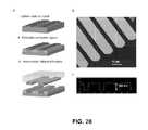
- FIG. 1is a schematic illustration of a general process for transfer printing solid objects.
- FIG. 1Aillustrates a feature on the surface of a donor substrate and a stamp in proximity to the donor substrate.
- the stampis brought in physical contact with at least a portion of the feature on the donor substrate and the stamp is subsequently quickly separated from the donor substrate such that the features are removed (e.g., separated from) from the donor substrate ( FIG. 1B ).
- FIG. 1Cdepicts the stamp containing the feature being brought into contact with a receiving substrate.
- the stampis slowly separated to transfer features from the stamp to the receiving substrate surface.
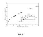
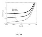
- FIG. 2graphically illustrates the rate dependence of stamp adhesion by evaluating the speed at which a steel cylinder rolls down an inclined slab of polydimethylsiloxane (PDMS) (see inset).
- the graphis a plot of the separation energy, or the Energy Release Rate G (J/m 2 ) as a function of Separation speed, v (cm/s).
- Separation speedis varied by changing the inclination angle of the PDMS slab, and the corresponding G is calculated by the loss of the cylinder's gravitational potential energy.
- Gvaries by more than an order of magnitude across the range of speeds measured in this demonstration. Consequently, transfer elements of PDMS adhere more strongly or weakly to printable features depending upon the speed separation.
- Appropriate separation speed ranges for retrieval and release of specific features from transfer elements in specific systemsmay be in principle be calculated by detailed modeling, but in practice, retrieval and release speed ranges are determined experimentally.
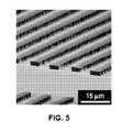
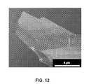
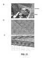
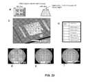
- FIG. 3provides photographs illustrating the effect of slow ( FIG. 3A ) and fast removal ( FIG. 3B ) of a PDMS stamp from micromachined silicon beams. Slow removal of a PDMS leaves the features intact ( FIG. 3A ) but the much higher adhesive force associated with fast (about 10 cm/s) stamp removal cleanly breaks the features from their anchor ( FIG. 3B ).
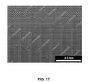
- FIG. 4is an image of a 30 mm ⁇ 38 mm array of about 24,000 silicon microstructures printed onto a 100-mm GaAs wafer by a corresponding “inked” PDMS stamp.
- the insetis an SEM image of a portion of the wafer. Analysis of the SEM images indicate that fewer than 100 microstructures are missing from the printed array.
- FIG. 5is an SEM image of GaN ribbons printed onto a silicon (100) wafer using the process of the present invention.
- FIG. 6is an SEM image of a multi-layer assembly generated by repeated printing of silicon features onto a silicon wafer.
- FIG. 7is an SEM image of p-type silicon features printed onto InP substrate.
- FIG. 8is an SEM image of n-type silicon features printed onto p-type silicon substrate.
- FIG. 9is an image of silicon structures printed onto a translucent hydrophilic (MgO) substrate.
- FIG. 10is a plot of current (amps) against bias (volts) for n-type silicon features printed directly onto a p-type silicon wafer by the present invention. Such printing followed by annealing forms p-n junctions that can carry 6.7 amps/cm 2 at a forward bias of 1 volt. The line is a best-fit to the experimentally obtained data points.
- FIG. 11is an image of 100-nm-thick muscovite (grade V-1 mica) ribbons cleaved at high separation rates from a mica substrate with a PDMS stamp, and then transfer-printed onto SiO 2 (blue) at a low separation rate.
- the inset profileoutlines an AFM line trace of the structures printed onto SiO 2 .
- FIG. 12is an image of a graphite sheet, ranging from less than about 3 to 12 nm thick, cleaved from a highly ordered pyrolytic graphite substrate and printed onto SiO 2 with a stamp using low separation rates.
- FIG. 13is an image of silica microspheres picked up from and subsequently printed onto silicon wafers by means of PDMS stamps and controlled separation rates. Relief features in the stamp define the stripe pattern on the substrate surface.
- FIG. 14is an image of African Violet pollen grains picked up from and subsequently printed onto silicon wafers by means of PDMS stamps and controlled separation rates.
- FIG. 15is an image of a printed array formed by rolling a cylindrical glass lens across a stamp inked with microstructures.
- the insetis an SEM image of the stamp inked with microstructures.
- FIG. 16is an image of a printed array formed by pressing a double-convex polycarbonate magnifying glass into the soft, inked stamp.
- FIG. 17is an image of silicon photodiodes printed on a spherical glass surface (p-doped regions seem brighter).
- FIG. 18is a plot of current as a function of voltage bias for various illumination conditions of printed silicon photodiodes similar to those in FIG. 17 .
- FIG. 19is an image of relatively large (about 1 mm) silicon features printed onto paper. Silicon features were removed from a donor substrate using fast separation rates to enable efficient retrieval onto a PDMS transfer element and then printed onto paper coated with a thin (about 10 micron) coat of PDMS coated with Ti/Au. The bottom surfaces of the silicon features were coated with Ti/Au such that strong binding between the paper and the features occurred through gold cold-welding.
- FIG. 20is a schematic of different means of separation of a transfer element from a receiving or donor substrate.
- A.depicts axis-symmetric separation.
- B and Cdepict non axis-symmetric separation, performed in a peeling motion in which the transfer element is peeled back (B), or in which the substrate is peeled away (C).
- D.illustrates another type of non axis-symmetric separation provided by applying a rolling force to a curved element, in this case a curved transfer element.
- FIG. 21 ( a )shows an actuator stage that moves donor and receiver substrates relative to a transfer element in the x-y plane and moves a transfer element in the z-direction with controllable separation rates (scale bar is 2 inches).
- (b) and (c)show scanning electron micrographs of silicon multilayer structures printed on silicon wafers printed by four successive repetitions of slow separation of a PDMS transfer element from the receiving substrate, transferring silicon features to the substrate one layer at a time.
- FIG. 22demonstrates the influence of separation rate on the efficiency of retrieval of silicon features from a donor substrate using the actuator stage shown in FIG. 21 ( a ).
- FIG. 22 ( a )is a drawing (not to scale) of a PDMS transfer element that is fixed to the actuator stage.
- (b)shows the donor substrate after successive retrieval experiments (labeled i-vi) at various separation rates, listed in (c).
- the rates listed in (c)are vertical separation rates and are not equal to the speed of the propagation of the boundary of the contacted region between the transfer element and the donor substrate (in the x-y plane of the donor substrate), which is generally much faster than the vertical separation rate in this configuration.
- (d), (e), and (f)show optical micrographs of the regions on the donor substrate after experiments i, iii, and iv, at vertical separation speeds of 1 cm/s, 1 ⁇ m/s, and 100 ⁇ m/s, respectively.
- the four lightly colored patches in (d)are regions from which nearly all of the features on the donor substrate were retrieved onto the transfer element due to the fast separation rates.
- (e)shows that no features were retrieved onto the transfer element at the slow vertical separation rate of 1 ⁇ m/s.
- (f)shows that at an intermediate separation rate (100 ⁇ m/s), only a few features are retrieved among the many in the region that was previously in contact between the donor substrate and the transfer element. Only those features in the center of the previously contacted region were retrieved off of the donor, where presumably the speed of the propagation of the contacted area boundary (in the x-y plane of the donor substrate) was greatest.
- FIG. 23demonstrates the effects of separation speed on the printing efficiency or quality of printing silicon features from a PDMS transfer element, as depicted in FIG. 22 ( a ) onto a silicon wafer coated with thin films of PDMS of various thicknesses.
- Printing qualityis measured by the approximate fraction of microstructures transferred to the thin PDMS films on a scale from 0 to 5 (0: ⁇ 1%; 1: 1% to 10%; 2: 11% to 50%; 3: 51% to 90%; 4: 91% to 99%; 5: >99%).
- the panels in Bare micrographs showing printing efficiency associated with quality scale 0, 1, 2, 3, 4, 4.5, and 5.
- FIG. 24shows micrographs of semiconductor (Si) features printed onto substrates using spin-on glass as a smoothing layer to facilitate transfer onto a receiving substrate.
- the smoothing layerallows (a) transfer with good efficiency and (b), (c) strong adhesion to the receiving substrate after suitable annealing.
- the micrographs in (b) and (c)show features transferred onto a silicon wafer coated with spin-on glass after annealing for several hours at 300° C. and subsequent breaking of the silicon wafer.
- the silicon featuresfracture along the same line as the fracture edge of the wafer, indicating robust binding between the wafer and the silicon features.
- FIG. 25shows a picture of a transfer element composed of a thin kapton backing coated with a thin layer of PDMS.
- the transfer elementis used in a roller configuration by wrapping it around a foam paint roller.
- the transfer elementhas on it silicon features retrieved from a donor substrate.
- FIG. 26demonstrates the ability to print a semiconductor feature onto a receiving substrate using a transfer element and a given separation rate (slow in this case) and to subsequently remove that feature using the same transfer element but with a different separation rate (in this case fast).
- (a)shows silicon features printed onto a topographically relief-structured silicon receiving substrate from a PDMS transfer element using slow (about 1 mm/s) separation speeds.
- (b)shows the same silicon topographically relief-structured silicon substrate after the printed silicon features have been removed using the same PDMS transfer element with a fast separation speed (greater than 10 cm/s).
- FIG. 27shows silicon features (hut-shaped) printed onto silicon by means of a Scotch® tape transfer element and slow separation speeds.
- FIG. 28Aillustrates a process for removing layers by applying a pattern mask on crystal (panel i); etching/softening unmasked regions (panel ii); contacting and removing the pattern layer with a kinetically-controllable elastomeric stamp (panel iii).
- B.is an SEM of thin mica printed onto SiO2 using the process outlined in A.
- C.is an AFM line trace of the cross-section of the mica ribbons printed onto SiO 2 using the process outlined in A.
- transferringor “transfer” relates to features, materials, structures, device components and/or integrated functional devices that are removed from the surface of one substrate and “printed” or applied to the surface of another substrate.
- featureis used broadly to refer to a material, structure, device component and/or functional device to be transferred, for example via printing techniques such as contact printing.
- the definition of featureencompasses any element that can be transferred from a donor substrate to a stamp and subsequently printed to a receiving surface including, but not limited to, semiconductor structures, metallic structures, ceramic structures, dielectric structures, composite structures.
- features of the present inventionare printable semiconductor elements and patterns of printable semiconductor elements.
- the structurecan be a three-dimensional pattern, having a pattern on a surface with a depth and/or height to the pattern.
- a featureencompasses geometrical features including, but not limited to, any two-dimensional pattern or shape (circle, triangle, rectangle, square), three-dimensional volume (any two-dimensional pattern or shape having a height/depth), as well as systems of interconnected etched “channels” or deposited “walls.”
- a featurecomprises a biological material or element.
- a featureis globular.
- a globular featurerefers to a generally rounded material, for example, microspheres, seeds and other curved objects.
- the dimensions of the featurecan be microsized, nanosized, or both microsized and nanosized.
- a microstructureis a feature with a dimension on the order of greater than a micron including millimeters and several millimeters.
- the transferred featurecomprises a plurality of silicon microstructures.
- a nanostructureis a feature with a dimension on the order of less than about one micron. In an embodiment, a nanosized feature is less than about 100 nm.
- a “lateral dimension”refers to a distance that is parallel to the contacting transfer surface and partner surface.
- a “vertical dimension”refers to the vertical height of the feature relative to the supporting surface.
- the featurecomprises “microstructures” and/or “nanostructures.”
- microstructuresand/or “nanostructures.”
- microstructuresand/or “microsized structures” are used synonymously, and the terms “nanostructures” and “nanosized structures” are used synonymously.
- nanostructuresrefer to structures having at least one dimension that is on the order of nanometers to microns, including in the range of tens of nanometers to hundreds of nanometers.
- the nanostructurehas at least one feature that is on the order of tens of nm or smaller.
- the width of the structurecan be on the order of 10's to 100's of nm and the length can be on the order of microns to 1000's of microns.
- the nanostructurehas one or more features that range from an order of tens of nm to hundreds of nm.
- microstructuresrefer to structures that are larger than nanostructures.
- a microstructurehas at least one feature physical dimension ranging from about 1 micron to about 5000 microns.
- Featureencompasses a layer or a layer portion, wherein the thickness of the layer or layer portion is between an order of nanometers to microns, including, but not limited to, between about 3 nm to 12 nm.
- Feature transfercan involve transfer of one or more of biologics, chemicals or geometrical elements.
- a biologicis a feature that has use in a device for studying biological systems and encompasses, DNA, RNA, proteins and polypeptides.
- a device of the present inventionis said to interact with a cell when the device can detect a physical property associated with the cell.
- the biologic or chemicalis integrated within another feature to facilitate transfer of the biologic or chemical from a donor surface to a transfer device surface, and then to a receiving surface.
- a “pattern”refers to a plurality of features that are deposited and/or etched on a donor surface. Accordingly, the term encompasses a plurality of geometrical features etched onto a surface, as well as a plurality of geometrical features deposited onto a surface and a plurality of geometrical features freestanding on a surface.
- the present methods and systemare capable of transfer printing patterns of structures, including the features discussed herein, having well defined and selected physical dimensions, spatial orientations and positions.
- Circuitrefers to a feature that is an electrical network and encompasses integrated circuits and arrays of integrated circuits.
- substraterefers to a material that has at least one surface that contains a feature or at least one surface for receiving a feature.
- the surface to receive a featureis smooth, preferably with a roughness less than about 3 nm over a 1 ⁇ m 2 region.
- An “elastomeric transfer device”refers to an elastomeric material having a surface that can receive as well as transfer a feature.
- Exemplary elastomeric transfer devicesinclude stamps, molds and masks. The transfer device affects and/or facilitates feature transfer from a donor material to a receiver material.
- “Elastomer” or “elastomeric”refers to a polymeric material which can be stretched or deformed and return to its original shape without substantial permanent deformation. Elastomers commonly undergo substantially elastic deformations.
- Exemplary elastomers useful in the present inventionmay comprise, polymers, copolymers, composite materials or mixtures of polymers and copolymers.
- Elastomeric layerrefers to a layer comprising at least one elastomer.
- Elastomeric layersmay also include dopants and other non-elastomeric materials.
- Elastomers useful in the present inventionmay include, but are not limited to, thermoplastic elastomers, styrenic materials, olefenic materials, polyolefin, polyurethane thermoplastic elastomers, polyamides, synthetic rubbers, silicon-based organic polymers including polydimethylsiloxane (PDMS), polybutadiene, polyisobutylene, poly(styrene-butadiene-styrene), polyurethanes, polychloroprene and silicones.
- PDMSpolydimethylsiloxane
- PDMSpolybutadiene
- polyisobutylenepoly(styrene-butadiene-styrene)
- polyurethanespolychloroprene and silicones.
- Contactrefers to the configuration of two or more surfaces such that a feature on the surface of one element is capable of transfer to another surface.
- a stamp or transfer deviceis in contact with a donor material when a transfer surface facing a donor surface is in physical contact with the donor surface.
- a transfer surfaceis in contact with a receiver substrate surface when the transfer surface physically contacts the receiver substrate surface.
- contactrefers to at least a portion of the feature is in physical contact with at least a portion of another surface.
- contactrefers to substantially all the features on a surface in contact with another surface. Elements are in physical contact when they are observable as touching. Preferably, physical contact occurs under an applied force to ensure uniform and intimate contact over the portion of contacting surfaces.
- Patternrefers to a pair of surfaces that have regions of physical contact and regions of no physical contact.
- a transfer device of the present inventionis said to have a “pattern of contacts” with a donor surface so as to generate an inked transfer surface having a surface with relief features.
- the transfer devicehas mechanical attributes and characteristics, including Young's modulus, compressibility modulus, flexural rigidity, that are optimized as known in the art to ensure suitable structures are obtained from any of the processes disclosed herein. At least a portion of the transfer device is elastomeric and/or viscoelastic so that the adhesive force between a solid object and the transfer device is rate-sensitive.
- “separation” and “peeling”are used synonymously and refer to a process at which a first surface in contact with a second surface is separated from the second surface. Separation may be carried out by vertical displacement, horizontal displacement, displacement initiated from the ends of two surfaces and displacement initiated from the interior of two surfaces.
- Separationencompasses axis-symmetric and non axis-symmetric (“axis-unsymmetric”) separation, as illustrated in FIG. 20 .
- the adhesive force between a feature and an elastomeric transfer device surfaceis usually, but not always, larger for faster separation rates.
- the transfer devicecomprises a single material, wherein the material is elastomeric. The material properties of the transfer device ensure that as the deposition and/or removal process proceeds, physical contact is maintained between the transfer device and surface during feature transfer.
- a force actuatoris connected to the transfer device for applying a constant and uniform force, and corresponding pressure, between the transfer device and partner substrate.
- a forceis said to be uniformly applied to a surface such that the pressure distribution between the transfer device's stamping surface and partner surface is substantially uniform, thereby ensuring the transfer device remains level relative to the partner surface.
- Removal of the transfer device from the partner substrateis by any means known in the art including, but not limited to, removal by hand or controllable displacement rate actuator (see FIGS. 20A and 21A ), so long as the rate of removal is controllable.
- Other methods for removal of the transfer elementinclude rolling ( FIG. 20D ) and/or peeling ( FIG. 20B-C ) methods in which a transfer device and donor or receiver substrate are separated by non axis-symmetric separation, e.g., by rolling, where one or more of the contacted bodies is contoured ( FIG. 20D ), and/or by peeling where one or more of the contacted bodies is flexible ( FIG. 20B or C).
- the transfer devicecomprises an elastomeric layer and at least one other material.
- transfer of “substantially all” the features in contact with the transfer surfacerefers to at least 90%, at least 95% and at least 99% of the features in contact with the transfer surface are transferred.
- a “multi-layered feature”refers to sequential printing of features onto a receiving surface so that a first printed layer corresponds to features on a first donor surface and a second printed layer corresponds to a second donor surface.
- the donor surfacescan be identical, and instead the transfer devices contacts different donor surface locations.
- substantially constant peeling rateand a “substantially constant separation rate” are used synonymously and refer to the rate of surface-feature separation that does not significantly vary over the separation or peeling time. “Substantially constant” refers to a rate that does not vary by more than 2% relative to the average separation and/or peeling rate during the separation and/or peel time, including variation of less than 1%.
- Printrelates to materials, structures, device components and/or integrated functional devices that are capable of transfer, assembly, patterning, organizing and/or integrating onto or into substrates, via printing techniques including but not limited to, contact printing and solution printing.
- Print semiconductor elementsof the present invention comprise semiconductor structures that are able to be assembled and/or integrated onto substrate surfaces, for example using by dry transfer contact printing and/or solution printing methods.
- printable semiconductor elements of the present inventionare unitary single crystalline, polycrystalline or microcrystalline inorganic semiconductor structures.
- printable semiconductor elementsare connected to a substrate, such as a mother wafer, via one or more bridge elements.
- a unitary structureis a monolithic element having features that are mechanically connected.
- Semiconductor elements of the present inventionmay be undoped or doped, may have a selected spatial distribution of dopants and may be doped with a plurality of different dopant materials, including P and N type dopants.
- the present inventionincludes microstructured printable semiconductor elements having at least one cross sectional dimension greater than or equal to about 1 micron and nanostructured printable semiconductor elements having at least one cross sectional dimension less than or equal to about 1 micron.
- Printable semiconductor elements useful in many applicationscomprises elements derived from “top down” processing of high purity bulk materials, such as high purity crystalline semiconductor wafers generated using conventional high temperature processing techniques.
- printable semiconductor elements of the present inventioncomprise composite structures having a semiconductor operational connected to at least one additional device component or structure, such as a conducting layer, dielectric layer, electrode, additional semiconductor structure or any combination of these.
- printable semiconductor elements of the present inventioncomprise stretchable semiconductor elements and/or heterogeneous semiconductor elements.
- “Supported by a substrate”refers to a structure that is present at least partially on a substrate surface or present at least partially on one or more intermediate structures positioned between the structure and the substrate surface.
- the term “supported by a substrate”may also refer to structures partially or fully embedded in a substrate.
- semiconductorrefers to any material that is a material that is an insulator at a very low temperature, but which has a appreciable electrical conductivity at a temperatures of about 300 Kelvin. In the present description, use of the term semiconductor is intended to be consistent with use of this term in the art of microelectronics and electrical devices.
- Semiconductors useful in the present inventionmay comprise element semiconductors, such as silicon, germanium and diamond, and compound semiconductors, such as group IV compound semiconductors such as SiC and SiGe, group III-V semiconductors such as AlSb, AlAs, Aln, AlP, BN, GaSb, GaAs, GaN, GaP, InSb, InAs, InN, and InP, group III-V ternary semiconductors alloys such as Al x Ga 1-x As, group II-VI semiconductors such as CsSe, CdS, CdTe, ZnO, ZnSe, ZnS, and ZnTe, group I-VII semiconductors CuCl, group IV-VI semiconductors such as PbS, PbTe and SnS, layer semiconductors such as Pbl 2 , MoS 2 and GaSe, oxide semiconductors such as CuO and Cu 2 O.
- group IV compound semiconductorssuch as SiC and SiGe
- group III-V semiconductorssuch as AlSb, Al
- semiconductorincludes intrinsic semiconductors and extrinsic semiconductors that are doped with one or more selected materials, including semiconductor having p-type doping materials and n-type doping materials, to provide beneficial electrical properties useful for a given application or device.
- semiconductorincludes composite materials comprising a mixture of semiconductors and/or dopants.
- Specific semiconductor materials useful for in some applications of the present inventioninclude, but are not limited to, Si, Ge, SiC, AlP, AlAs, AlSb, GaN, GaP, GaAs, GaSb, InP, InAs, GaSb, InP, InAs, InSb, ZnO, ZnSe, ZnTe, CdS, CdSe, ZnSe, ZnTe, CdS, CdSe, CdTe, HgS, PbS, PbSe, PbTe, AlGaAs, AlInAs, AlInP, GaAsP, GaInAs, GaInP, AlGaAsSb, AlGaInP, and GaInAsP.
- Porous silicon semiconductor materialsare useful for applications of the present invention in the field of sensors and light emitting materials, such as light emitting diodes (LEDs) and solid state lasers.
- Impurities of semiconductor materialsare atoms, elements, ions and/or molecules other than the semiconductor material(s) themselves or any dopants provided to the semiconductor material. Impurities are undesirable materials present in semiconductor materials which may negatively impact the electrical properties of semiconductor materials, and include but are not limited to oxygen, carbon, and metals including heavy metals. Heavy metal impurities include, but are not limited to, the group of elements between copper and lead on the periodic table, calcium, sodium, and all ions, compounds and/or complexes thereof.
- Conformal contactrefers to contact established between surfaces, coated surfaces, and/or surfaces having materials deposited thereon which may be useful for transferring, assembling, organizing and integrating structures (such as printable semiconductor elements) on a substrate surface, such as a receiving substrate surface.
- conformal contactinvolves a macroscopic adaptation of one or more contact surfaces of an elastomeric transfer device to the overall shape of a substrate surface.
- conformal contactinvolves a microscopic adaptation of one or more contact surfaces of an elastomeric transfer device to a substrate surface leading to an intimate contact with out voids. The term conformal contact is intended to be consistent with use of this term in the art of soft lithography.
- Conformal contactmay be established between one or more bare contact surfaces of an elastomeric transfer device and a substrate surface.
- conformal contactmay be established between one or more coated contact surfaces, for example contact surfaces having a transfer material, printable semiconductor element, device component, and/or device deposited thereon, of an elastomeric transfer device and a substrate surface.
- conformal contactmay be established between one or more bare or coated contact surfaces of an elastomeric transfer device and a substrate surface coated with a material such as a transfer material, solid photoresist layer, prepolymer layer, liquid, thin film or fluid
- “Placement accuracy”refers to the ability of a transfer method or device to transfer a printable element, such as a printable semiconductor element, to a selected position, either relative to the position of other device components, such as electrodes, or relative to a selected region of a receiving surface.
- “Good placement” accuracyrefers to methods and devices capable of transferring a printable element to a selected position relative to another device or device component or relative to a selected region of a receiving surface with spatial deviations from the absolutely correct position less than or equal to 50 microns, more preferably less than or equal to 20 microns for some applications and even more preferably less than or equal to 5 microns for some applications.
- the present inventionprovides devices comprising at least one printable element transferred with good placement accuracy.
- “Fidelity”refers to a measure of how well a selected pattern of elements, such as a pattern of printable semiconductor elements, is transferred to a receiving surface of a substrate.
- Good fidelityrefers to transfer of a selected pattern of elements wherein the relative positions and orientations of individual elements are preserved during transfer, for example wherein spatial deviations of individual elements from their positions in the selected pattern are less than or equal to 500 nanometers, more preferably less than or equal to 100 nanometers.
- Young's modulusis a mechanical property of a material, device or layer which refers to the ratio of stress to strain for a given substance. Young's modulus may be provided by the expression;
- High Young's modulus(or “high modulus”) and low Young's modulus (or “low modulus”) are relative descriptors of the magnitude of Young's modulus in a give material, layer or device.
- a high Young's modulusis larger than a low Young's modulus, preferably about 10 times larger for some applications, more preferably about 100 times larger for other applications and even more preferably about 1000 times larger for yet other applications.
- Polymerrefers to a molecule comprising a plurality of repeating chemical groups, typically referred to as monomers. Polymers are often characterized by high molecular masses. Polymers useable in the present invention may be organic polymers or inorganic polymers and may be in amorphous, semi-amorphous, crystalline or partially crystalline states. Polymers may comprise monomers having the same chemical composition or may comprise a plurality of monomers having different chemical compositions, such as a copolymer. Cross linked polymers having linked monomer chains are particularly useful for some applications of the present invention.
- Polymers useable in the methods, devices and device components of the present inventioninclude, but are not limited to, plastics, elastomers, thermoplastic elastomers, elastoplastics, thermostats, thermoplastics and acrylates.
- Exemplary polymersinclude, but are not limited to, acetal polymers, biodegradable polymers, cellulosic polymers, fluoropolymers, nylons, polyacrylonitrile polymers, polyamide-imide polymers, polyimides, polyarylates, polybenzimidazole, polybutylene, polycarbonate, polyesters, polyetherimide, polyethylene, polyethylene copolymers and modified polyethylenes, polyketones, poly(methyl methacrylate, polymethylpentene, polyphenylene oxides and polyphenylene sulfides, polyphthalamide, polypropylene, polyurethanes, styrenic resins, sulphone based resins, vinyl-based resins or any combinations of these.
- registered transferrefers to concerted processes that maintain the relative spatial orientation of transferred elements, preferably to with about 50% and more preferably for some application to within about 1%.
- Registered processes of the present inventionmay also refer to the ability of methods of the present invention to transfer, assemble and/or integrate printable semiconductor elements to specific regions of a receiving substrate preselected to within 100 microns and preferably for some embodiments to with 50 nanometers
- Bridge elementsare alignment maintaining elements which connect a feature, such as printable semiconductor elements, to a donor substrate, such as a semiconductor wafer.
- a bridge elementis a partially or fully undercut structure that connects one or more ends of the feature to a donor substrate.
- a bridge elementconnects the bottom of a feature to the donor substrate.
- Bridge elementsare useful for maintaining selected orientations and/or positions of features, such as printable semiconductor elements, during transfer, assembly and/or integration processing steps. Bridge elements are also useful for maintaining relative positions and orientations of a pattern or array of features, such as printable semiconductor elements, during transfer, assembly and/or integration processing steps.
- bridge elementspreserve the positions and spatial orientations of features, such as printable semiconductor elements, during contact, bonding and transfer processes involving a contact surface of a transfer device, such as a conformable elastomeric stamp, thereby enabling registered transfer from a mother wafer to the transfer device.
- Bridge elements in this aspect of the present inventionare capable of disengaging from the printable semiconductor elements without significantly changing the positions and orientations of the printable semiconductor elements upon contact and/or movement of the transfer device. Disengagement is typically achieved by fracture of the bridge elements during contact and/or movement of the transfer device.
- This inventionprovides methods for transferring features, including micropatterns, nanopatterns and a combination of micro and nanopatterns.
- the present inventionprovides methods of patterning by elastomeric stamping, to provide relief and/or recess features directly to a surface.
- the viscoeleastic nature of the surface material on the transfer deviceleads to a separation force (i.e. the force that can lift objects from a surface) that depends on separation rate.
- this forceis large enough to remove objects from a substrate and transfer them onto a transfer device, even when the static surface energy of the transfer device is lower than that of the substrate. At low separation rates, this separation force is low.
- FIG. 1schematically illustrates a process for transfer printing solid objects from one substrate to another.
- FIG. 1Aillustrates the start of the process wherein the donor substrate 20 that supports fully formed, organized arrays of solid objects (“features” 40 ) (for example, devices, materials, elements, biological entities, etc.) is prepared.
- the donor substratecan be prepared using top-down fabrication, bottom-up growth, self-assembly or other means.
- Contacting a soft elastomeric transfer device (stamp) 10 against these solid objectsleads to conformal contact, driven by generalized adhesion forces that are typically dominated by van derWaals interactions.
- the adhesion between the features 40 and the transfer surface 15is rate-sensitive (that is, kinetically controllable) owing to the viscoelastic behavior of the elastomer separating the transfer device 10 from the donor substrate 20 with sufficiently high separation velocity (typically about 10 cm/s or faster for the systems presented herein) leads to adhesion that is sufficient to adhere preferentially the features 40 to the surface 15 of the transfer device 10 , lifting them off the donor substrate surface 25 ( FIG. 1B ).
- the transfer device 10now ‘inked’ with these features 40 , is brought into contact with a receiving (device) substrate 30 ( FIG. 1C ).
- Removing the transfer device 10 with sufficiently low separation velocitycauses the features 40 to adhere preferentially to the receiving substrate surface 35 and separate from the transfer surface 15 ( FIG. 1D ).
- the transfercan be carried out uniformly with a flat stamp or with a structured element that contacts and transfers only some set of objects from the donor substrate.
- the embodiment illustrated in FIG. 1depicts the flat surfaces (when the surfaces are unstressed). As discussed herein below, however, any of the transfer surface 15 , donor surface 25 , and receiving surface 35 can be curved (see FIG. 20D ).
- the wafersare treated with (tridecafluoro-1,1,2,2-tetrahydrooctyl)-1-trichlorosilane (United Chemical Technologies) for 1 h in a vacuum desiccator to facilitate the removal of the PDMS slab.
- the slabis placed against a sturdy inclined glass plate, the inclination of which is measured relative to a level countertop.
- a steel cylinder(McMaster-Carr, diameter 12.7 mm, length 75.5 mm, 75.2 g) is placed at the top of the slab and allowed to roll.
- the slabis cleaned with a lint roller (3M) between successive roll tests. Rolling speed is measured with a ruler and a stopwatch. Video footage is captured and analyzed to confirm that the cylinder rolled against the slab at a constant speed.
- a steel cylinder rolling down an inclined slab of PDMS rubberreaches a terminal velocity, where gravity works to separate the steel from the PDMS at the trailing edge of the contact region.
- the loss in gravitational potentialis taken as the adhesion energy hysteresis (the difference between the work required to separate the steel from the PDMS and the energy evolved at the advancing contact edge) at the measured rolling or separation speed v.
- the energy associated with the advancing contact area at the front of the rolling cylinderis typically small, so the adhesion energy hysteresis is taken as the separation energy, or the energy release rate, G.
- FIG. 2shows the dependence of G on v. For the range of speeds measured here (0.02 to 4.8 cm/s), the energy release rate varies by more than an order of magnitude.
- the separation energy for the microstructure-substrate interface G substrateis typically independent of rate.
- G PDMSincreases relative to G substrate until the elastomer-microstructure interface becomes strong enough to break the microstructure-substrate interface. Determining which interface fails depends on the geometry of the microstructures and can be established by energy-based arguments similar to those used to compare competing fracture modes in layered materials. Geometrical design considerations can be useful in guiding the transfer of microstructures, for example by providing stress concentration zones to facilitate controlled fracture or by engineering contact zone areas to alter levels of adhesion.
- a key concept for the transfer-printing criteriais the strongly rate-dependent separation energy of solid objects from an elastomer and the rate-independent separation of solid objects from a substrate interface.
- FIG. 3provides an example of a feature that can be transferred from a donor substrate to a stamp.
- FIG. 3Ashows freestanding silicon beams micromachined from a silicon-on-insulator (SOI) wafer, connected to an unetched part of the wafer that anchors their ends.
- SOIsilicon-on-insulator
- FIGS. 22 and 23The effect of separation speed on efficiency of feature removal is shown in FIGS. 22 and 23 . At a higher separation speed, more features are removed (compare FIG. 22 d - f ).
- FIG. 23Aalso illustrates the effect of the thickness of an elastomer layer or film (in this case PDMS) on printing efficiency
- FIG. 4shows a 30 mm ⁇ 38 mm GaAs wafer printed with an array of I-shaped silicon microstructures (see inset) by a single elastomeric stamp.
- an inked elastomeric stampprints the pattern in ambient conditions directly onto a 100-mm GaAs wafer.
- This arraycontains about 24,000 microstructures; the yield of the entire process, including micromachining, pick-up and printing, is more than 99.5% (corresponding to fewer than 100 microstructures missing from the array).
- Particles on the surface of the receiving substrateare typically the most significant cause of defects. With care, including careful processing and handling of the receiving substrate, printing efficiency can approach 100%.
- the printing processes disclosed hereinhave the potential for area multiplication, where a single donor substrate of a given area supplies microstructures to several receiving substrates of the same area or a single receiving substrate with a substantially larger area. This capability is important when the printed material is costly and where large-area, sparse coverage is desired.
- GaN microstructuresprepared as described hereinbelow
- printed onto silicon (100)is an example of one of these systems.
- an embodiment of the present inventionencompasses repeated printing. Such repeated printing steps, results in easy fabrication of large-area or even multilayer assemblies ( FIG. 6 ) with few processing steps, and can be used in a variety of applications including, but not limited to, applications such as photonic bandgap materials or multilayer electronic systems.
- the techniques disclosed hereincan print objects with a wide range of shapes and sizes onto virtually any smooth substrate.
- FIG. 7shows submicrometer (0.3 ⁇ m ⁇ 20 ⁇ m ⁇ 0.1 ⁇ m) silicon structures printed onto InP using the present invention.
- the ability of the present invention to deposit nanostructures and/or microstructures having scale on the order of nanometers and/or micrometersindicate that stamp-based transfer printing is useful for the production of device-scale or smaller objects.
- the inventionencompasses printing larger sizes (e.g. 100 ⁇ m ⁇ 100 ⁇ m ⁇ 2.5 ⁇ m). Such printing size is useful for structures to support elaborate circuits ( FIG. 8 ). Yields for printing large objects are generally lower than for small objects, as a single asperity between a printed object and receiving substrate can impede transfer. Nevertheless, yields of 95% or better are achievable for all of the wafer-generated geometries presented herein when the receiving substrate is smooth, even when the printing is performed outside a cleanroom environment. Substrates with surface roughness of less than about 3 nm over 1 ⁇ m 2 can function as effective surfaces for receiving structures from an elastomeric stamp, largely independent of chemical composition or surface energy.
- silicon microstructurescan reliably transfer onto either hydrophilic surfaces, such as SiO 2 , NaCl and MgO ( FIG. 9 ), or hydrophobic surfaces including, but not limited to, polystyrene or silicon freshly stripped of its native oxide. As surface roughness increases beyond 3 nm over 1 ⁇ m 2 , yields generally decrease.
- the present inventionprovides reliable printing without the use of conventional adhesives or specialized surface chemistries. This is important in the context of wafer-based microstructure printing because it allows moderate-to-high-temperature processing ( ⁇ 150° C. and above) and good electrical contact between the printed structure and the receiving substrate.
- Printed p-n junctions formed by transferring n-type silicon microstructures to a p-type silicon substrateexploit both of these features. Annealing and metallization of the junction produces a rectifying device with characteristics reasonably well described by a fit for a monolithic p-n junction as the applied bias sweeps from ⁇ 1 to 1 V ( FIG. 10 ). The fit in FIG.
- FIG. 11shows, as an example, a pattern of thin high-quality muscovite (grade V-1 mica) printed by removing a stamp in contact with the mica at sufficiently high separation rates to cleave patterned ribbons from a donor substrate of bulk mica.
- PDMS stampscan also cleave sheets from unpatterned grade V-1 mica or graphite ( FIG.
- stamp-microstructure interfaceis strong enough at high separation rates to remove structures bound to a donor substrate at least as strongly as 6 J/m 2 .
- the high adhesive strength present at high separation ratesreduces to minimal levels at low rates.
- the transfer devices disclosed hereincan pick-up and release, for example, highly non-planar, globular structures, such as silica microspheres ( FIG. 13 ) and grains of pollen ( FIG. 14 ), which have very small areas of contact to rigid receiving substrates.
- Non-planar printingproceeds by rolling a cylindrical substrate across, or by pressing a spherical substrate against, a flat, compliant stamp.
- FIG. 15shows arrays of silicon microstructures printed onto a cylindrical glass lens.
- FIG. 16shows arrays of silicon microstructures printed onto a low-cost spherical polycarbonate lens.
- FIG. 17illustrates fully functional single-crystal silicon photodiodes printed onto a glass lens with the current-voltage characteristics of a typical device ( FIG. 18 ).
- Such non-planar microfabricationis valuable for applications including light detection and energy generation on curved focusing or imaging optics.
- silicon microstructuresare generated from SOI wafers (Shin-Etsu, top silicon 3.0 ⁇ m, buried oxide 1.1 ⁇ m, n-type resistivity 5-20 ⁇ cm; or Soitec, top silicon 100 nm, buried oxide 200 nm, p-type) patterned by conventional photolithography and phase-shift photolithography 27 with Shipley 1805 photoresist (PR).
- the top siliconis etched by SF 6 plasma (30 mtorr, 40 s.c.c.m.
- SF6, 50Wusing PR as an etch mask or by aqueous KOH (20 wt %, 100° C.) using an etch mask of Ti/Au (3/30 nm) deposited by electron-beam evaporation.
- Ti/Au etch masksare removed after KOH etching using KI/I 2 (2.67/0.67 wt %) in water. The buried oxide is then etched in concentrated HF.
- GaN microstructuresare generated from a GaN-on-silicon (111) wafer (Nitronex).
- the nitrideis etched in an inductively coupled plasma reactive ion etcher (3 mtorr, 15 s.c.c.m. Cl 2 , 5 s.c.c.m. Ar, ⁇ 100 V bias) using PECVD SiO x (500 nm) and Cr (150 nm) as an etch mask.
- Microstructuresare then undercut by etching the silicon in aqueous KOH (20 wt %, 100° C.).
- Micagrade V-1, Structure Probe
- an inductively coupled plasma reactive ion etcher3 mtorr, 15 s.c.c.m. BCl 3 , 5 s.c.c.m. Ar, ⁇ 90 V bias
- electron-beam evaporated Cr100 nm
- PRPR
- Silica microsphere filmsare prepared by casting droplets of IPA and an aqueous suspension of microspheres onto a silicon wafer and allowing them to dry. Pollen films are also prepared by suspension casting and drying on a silicon wafer.
- PDMS Transfer PreparationPDMS stamps (Dow-Sylgard 184) are cast against flat substrates (for example, polystyrene petri dishes, Fisher Scientific) and cut to dimensions typically about 2 cm ⁇ 2 cm ⁇ 7 mm thick. Stamps are laminated against donor substrates such that conformal contact is achieved and subsequently removed manually in a peeling manner such that the delamination front traveled at 10 cm/s or faster. The stamps thus ‘inked’ with objects from the donor are then laminated against receiving substrates and subsequently removed by slow (about 1 mm/s) manual separation or peeling to complete the transfer-printing process.
- flat substratesfor example, polystyrene petri dishes, Fisher Scientific
- Printed Junction Diode FabricationSOI chips (Shin-Etsu) are heavily n-doped at the top surface with spin-on-dopant (Zhue et al.) (P509, Filmtronics) and activation at 950° C. for 5 s. Microstructures generated as described above are printed onto boron-doped test-grade silicon chips (Montco, resistivity 1-100 ⁇ cm). Before printing, the receiving substrate is dipped in about 1% HF to remove native oxide, rinsed with deionized water and dried in N 2 . The printed junction is then annealed for 2 min at 600° C. in N 2 . Metal contacts are defined by photolithography with Shipley 1818 and lift-off of electron-beam-evaporated Al/Au (20/50 nm). The contacts are made non-rectifying by 4 min of annealing at 500° C.
- Silicon photodiodesare generated from an n-type SOI wafer (Shin-Etsu) with selected areas highly n-doped (P509, Filmtronics) and other areas highly p-doped (B-75 ⁇ , Honeywell). Doped regions are defined using windows in a spin-on glass (700B, Filmtronics) and the dopants are activated by annealing as described above (Zhu et al.) for the printed junction fabrication, first n-type, then p-type. Structures are subsequently micromachined using SF6 plasma and undercut with HF.
- Another aspect of the inventionis using the elastomeric and/or viscoelastic transfer devices of the present invention to transfer layers, wherein the depth or thickness of the transferred layer is kinetically controllable ( FIG. 28 ).
- the faster the separation ratethe greater the transfer layer thickness. Accordingly, by controlling the separation rate, the thickness or depth of the transfer layer is controlled.
- the composition of the transfer layeris a material that comprises layers including, but not limited to, graphite, graphene and mica.
- the layerscan have a structure comprising a series of repeating planar layers, as for graphite, wherein the layers are bound by van der Waals interactions.
- the present methodsare also useful for transferring material and structures from materials comprising a series of nonplanar layers.
- the layerscan also be bound by any one or more of other forces, including London, hydrogen bonding, covalent bonding and ionic bonding. The magnitude of bonding between layers will affect the separation rate required to lift-off a layer of a certain depth, with layers having stronger adhesion requiring higher separation rates.
- FIG. 28Asummarizes the general process.
- an appropriate external surface of a substrate comprising a layered structuresuch as graphite, graphene or mica, for example, is patterned masked.
- the patternis one or more masked regions having selected physical dimensions, spatial orientations and positions.
- Exemplary patternscomprise ribbons, platelets, strips, discs or any combination of these.
- the geometry and physical dimensions of the mask regions in this embodimentdefines the geometry and physical dimensions of the features that are to be transferred.
- the unmasked regionsare then etched and/or softened by dry or wet processes to chemically alter the unmasked region.
- the mask on the external surface of the substratecan be optionally removed.
- An elastomeric deviceis brought into contact with the pattern for lifting off or releasing the pattern. By varying the separation rate of the transfer surface with the pattern, the thickness of the transfer pattern is varied. This is shown for a graphite layer ( FIG. 12 ), as well as a mica layer ( FIGS. 28 b and c
- the depth of the lift-off pattern or layer(s)depends on a number of factors, including: (i) the physical dimension of the masked region; (ii) the composition of the pattern; (iii) the etching or chemical alternation system employed; and (iv) the kinetic rate or separation rate of the transfer device from the donor surface containing the pattern, with faster pull-off rates resulting in a larger number of layers that lift-off and are transferred to the transfer surface device.
Landscapes
- Engineering & Computer Science (AREA)
- Chemical & Material Sciences (AREA)
- Nanotechnology (AREA)
- Physics & Mathematics (AREA)
- Mathematical Physics (AREA)
- Theoretical Computer Science (AREA)
- Crystallography & Structural Chemistry (AREA)
- Manufacturing Of Printed Wiring (AREA)
- Thin Film Transistor (AREA)
Abstract
Description
wherein E is Young's modulus, L0is the equilibrium length, ΔL is the length change under the applied stress, F is the force applied and A is the area over which the force is applied. In an embodiment, Young's modulus varies with stress. Young's modulus may also be expressed in terms of Lame constants via the equation:
wherein λ and μ are Lame constants. High Young's modulus (or “high modulus”) and low Young's modulus (or “low modulus”) are relative descriptors of the magnitude of Young's modulus in a give material, layer or device. In the present invention, a high Young's modulus is larger than a low Young's modulus, preferably about 10 times larger for some applications, more preferably about 100 times larger for other applications and even more preferably about 1000 times larger for yet other applications.
GPDMS=
- 1. Georgakilas, A. et al. Wafer-scale integration of GaAs optoelectronic devices with standard Si integrated circuits using a low-temperature bonding procedure. Appl. Phys. Lett. 81, 5099-5101 (2002).
- 2. Yeh, H.-J. J. & Smith, J. S. Fluidic self-assembly for the integration of GaAs light-emitting diodes on Si substrates. IEEE Photon. Technol. Lett. 6, 706-708 (1994).
- 3. Ambrosy, A., Richter, H., Hehmann, J. & Ferling, D. Silicon motherboards for multichannel optical modules. IEEE Trans. Compon. Pack. A 19, 34-40 (1996).
- 4. Lambacher, A. et al. Electrical imaging of neuronal activity by multi-transistor-array (MTA) recording at 7.8 μm resolution. Appl. Phys. A 79, 1607-1611 (2004).
- 5. Menard, E., Lee, K. J., Khang, D.-Y., Nuzzo, R. G. & Rogers, J. A. A printable form of silicon for high performance thin film transistors on plastic substrates. Appl. Phys. Lett. 84, 5398-5400 (2004).
- 6. Zhu, Z.-T., Menard, E., Hurley, K., Nuzzo, R. G. & Rogers, J. A. Spin on dopants for high-performance single-crystal silicon transistors on flexible plastic substrates. Appl. Phys. Lett. 86, 133507 (2005).
- 7. Sun, Y. & Rogers, J. A. Fabricating semiconductor nano/microwires and transfer printing ordered arrays of them onto plastic substrates. Nano Lett. 4, 1953-1959 (2004).
- 8. Jacobs, H. O., Tao, A. R., Schwartz, A., Gracias, D. H. & Whitesides, G. M. Fabrication of a cylindrical display by patterned assembly. Science 296, 323-325 (2002).
- 9. Reuss, R. H. et al. Macroelectronics: Perspectives on technology and applications. Proc. IEEE 93, 1239-1256 (2005).
- 10. Haisma, J. & Spierings, G. A. C. M. Contact bonding, including direct-bonding in a historical and recent context of materials science and technology, physics and chemistry-historical review in a broader scope and comparative outlook. Mater. Sci. Eng. R 37, 1-60 (2002).
- 11. Zheng, W. & Jacobs, H. O. Shape- and solder-directed self-assembly to package semiconductor device segments. Appl. Phys. Lett. 85, 3635-3637 (2004).
- 12. Bowden, N., Terfort, A., Carbeck, J. &Whitesides, G. M. Self-assembly of mesoscale objects into ordered two-dimensional arrays. Science 276, 233-235 (1997).
- 13. O'Riordan, A., Delaney, P. & Redmond, G. Field configured assembly: programmed manipulation and self-assembly at the mesoscale. Nano Lett. 4, 761-765 (2004).
- 14. Tanase, M. et al. Magnetic trapping and self-assembly of multicomponent nanowires. J. Appl. Phys. 91, 8549-8551 (2002).
- 15. Hsia, K. J. et al. Collapse of stamps for soft lithography due to interfacial adhesion. Appl. Phys. Lett. 86, 154106 (2005).
- 16. Huang, Y. Y. et al. Stamp collapse in soft lithography. Langmuir 21, 8058-8068 (2005).
- 17. Roberts, A. D. Looking at rubber adhesion. Rubber Chem. Technol. 52, 23-42 (1979).
- 18. Barquins, M. Adherence, friction and wear of rubber-like materials. Wear 158, 87-117 (1992).
- 19. Shull, K. R., Ahn, D., Chen, W.-L., Flanigan, C. M. & Crosby, A. J. Axisymmetric adhesion tests of soft materials. Macromol. Chem. Phys. 199, 489-511 (1998).
- 20. Brown, H. R. The adhesion between polymers. Annu. Rev. Mater. Sci. 21, 463-489 (1991).
- 21. Deruelle, M., L'eger, L. & Tirrell, M. Adhesion at the solid-elastomer interface: influence of interfacial chains. Macromolecules 28, 7419-7428 (1995).
- 22. Hutchinson, J. W. & Suo, Z. Mixed mode cracking in layered materials. Adv. Appl. Mech. 29, 63-191 (1992).
- 23. Lee, K. J. et al. Large-area, selective transfer of microstructured silicon (μs-Si): a printing-based approach to high-performance thin-film transistors supported on flexible substrates. Adv. Mater. 17, 2332-2336 (2005).
- 24. Aoki, K. et al. Microassembly of semiconductor three dimensional photonic crystals. Nature Mater. 2, 117-121 (2003).
- 25. Noda, S., Yamamoto, N. & Sasaki, A. New realization method for three-dimensional photonic crystal in optical wavelength region. Jpn J. Appl. Phys. 35, L909-L912 (1996).
- 26. Horn, R. G. & Smith, D. T. Contact electrification and adhesion between dissimilar materials. Science 256, 362-364 (1992).
- 27. Rogers, J. A., Paul, K. E., Jackman, R. J. & Whitesides, G. M. Using an elastomeric phase mask for sub-100 nm photolithography in the optical near field. Appl. Phys. Lett. 70, 2658-2660 (1997).
Claims (40)
Priority Applications (1)
| Application Number | Priority Date | Filing Date | Title |
|---|---|---|---|
| US11/423,192US7943491B2 (en) | 2004-06-04 | 2006-06-09 | Pattern transfer printing by kinetic control of adhesion to an elastomeric stamp |
Applications Claiming Priority (8)
| Application Number | Priority Date | Filing Date | Title |
|---|---|---|---|
| US57707704P | 2004-06-04 | 2004-06-04 | |
| US60106104P | 2004-08-11 | 2004-08-11 | |
| US65030505P | 2005-02-04 | 2005-02-04 | |
| US66339105P | 2005-03-18 | 2005-03-18 | |
| US67761705P | 2005-05-04 | 2005-05-04 | |
| US11/145,542US7557367B2 (en) | 2004-06-04 | 2005-06-02 | Stretchable semiconductor elements and stretchable electrical circuits |
| US11/145,574US7622367B1 (en) | 2004-06-04 | 2005-06-02 | Methods and devices for fabricating and assembling printable semiconductor elements |
| US11/423,192US7943491B2 (en) | 2004-06-04 | 2006-06-09 | Pattern transfer printing by kinetic control of adhesion to an elastomeric stamp |
Related Parent Applications (1)
| Application Number | Title | Priority Date | Filing Date |
|---|---|---|---|
| US11/145,542Continuation-In-PartUS7557367B2 (en) | 2004-06-04 | 2005-06-02 | Stretchable semiconductor elements and stretchable electrical circuits |
Publications (2)
| Publication Number | Publication Date |
|---|---|
| US20090199960A1 US20090199960A1 (en) | 2009-08-13 |
| US7943491B2true US7943491B2 (en) | 2011-05-17 |
Family
ID=40937875
Family Applications (1)
| Application Number | Title | Priority Date | Filing Date |
|---|---|---|---|
| US11/423,192Active2029-03-10US7943491B2 (en) | 2004-06-04 | 2006-06-09 | Pattern transfer printing by kinetic control of adhesion to an elastomeric stamp |
Country Status (1)
| Country | Link |
|---|---|
| US (1) | US7943491B2 (en) |
Cited By (214)
| Publication number | Priority date | Publication date | Assignee | Title |
|---|---|---|---|---|
| US20100178722A1 (en)* | 2008-10-07 | 2010-07-15 | De Graff Bassel | Methods and applications of non-planar imaging arrays |
| US20110171813A1 (en)* | 2006-09-20 | 2011-07-14 | The Board Of Trustees Of The University Of Illinois | Release Strategies for Making Transferable Semiconductor Structures, Devices and Device Components |
| US8389862B2 (en) | 2008-10-07 | 2013-03-05 | Mc10, Inc. | Extremely stretchable electronics |
| US8394706B2 (en) | 2004-06-04 | 2013-03-12 | The Board Of Trustees Of The University Of Illinois | Printable semiconductor structures and related methods of making and assembling |
| US20130069275A1 (en)* | 2011-09-20 | 2013-03-21 | Etienne Menard | Printing transferable components using microstructured elastomeric surfaces with pressure modulated reversible adhesion |
| US8440546B2 (en) | 2004-06-04 | 2013-05-14 | The Board Of Trustees Of The University Of Illinois | Methods and devices for fabricating and assembling printable semiconductor elements |
| US8536667B2 (en) | 2008-10-07 | 2013-09-17 | Mc10, Inc. | Systems, methods, and devices having stretchable integrated circuitry for sensing and delivering therapy |
| US8666471B2 (en) | 2010-03-17 | 2014-03-04 | The Board Of Trustees Of The University Of Illinois | Implantable biomedical devices on bioresorbable substrates |
| US8674911B2 (en) | 2011-01-31 | 2014-03-18 | Global Oled Technology Llc | Electroluminescent device aging compensation with multilevel drive |
| US8679888B2 (en) | 2008-09-24 | 2014-03-25 | The Board Of Trustees Of The University Of Illinois | Arrays of ultrathin silicon solar microcells |
| US8722458B2 (en) | 2007-01-17 | 2014-05-13 | The Board Of Trustees Of The University Of Illinois | Optical systems fabricated by printing-based assembly |
| US8886334B2 (en) | 2008-10-07 | 2014-11-11 | Mc10, Inc. | Systems, methods, and devices using stretchable or flexible electronics for medical applications |
| US20140335328A1 (en)* | 2011-06-29 | 2014-11-13 | Lg Innotek Co., Ltd. | Nanowire manufacturing device having nanowire manufacturing substrate and nanowire adhesive film and nanowire manufactured using the same |
| US8916451B2 (en) | 2013-02-05 | 2014-12-23 | International Business Machines Corporation | Thin film wafer transfer and structure for electronic devices |
| US8934965B2 (en) | 2011-06-03 | 2015-01-13 | The Board Of Trustees Of The University Of Illinois | Conformable actively multiplexed high-density surface electrode array for brain interfacing |
| US9059013B2 (en) | 2013-03-21 | 2015-06-16 | International Business Machines Corporation | Self-formation of high-density arrays of nanostructures |
| US9067393B2 (en) | 2012-10-29 | 2015-06-30 | Industrial Technology Research Institute | Method of transferring carbon conductive film |
| US9105555B2 (en) | 2004-06-04 | 2015-08-11 | The Board Of Trustees Of The University Of Illinois | Stretchable form of single crystal silicon for high performance electronics on rubber substrates |
| US9123614B2 (en) | 2008-10-07 | 2015-09-01 | Mc10, Inc. | Methods and applications of non-planar imaging arrays |
| US9159635B2 (en) | 2011-05-27 | 2015-10-13 | Mc10, Inc. | Flexible electronic structure |
| US9171794B2 (en) | 2012-10-09 | 2015-10-27 | Mc10, Inc. | Embedding thin chips in polymer |
| WO2015184088A1 (en)* | 2014-05-28 | 2015-12-03 | The Trustees Of The University Of Pennsylvania | Surfaces with tunable adhesion based on composite structures and methods of making the same |
| WO2015193435A1 (en) | 2014-06-18 | 2015-12-23 | X-Celeprint Limited | Systems and methods for controlling release of transferable semiconductor structures |
| US9289132B2 (en) | 2008-10-07 | 2016-03-22 | Mc10, Inc. | Catheter balloon having stretchable integrated circuitry and sensor array |
| US9324733B2 (en) | 2004-06-04 | 2016-04-26 | The Board Of Trustees Of The University Of Illinois | Controlled buckling structures in semiconductor interconnects and nanomembranes for stretchable electronics |
| US9358775B2 (en) | 2014-07-20 | 2016-06-07 | X-Celeprint Limited | Apparatus and methods for micro-transfer-printing |
| US9368683B1 (en) | 2015-05-15 | 2016-06-14 | X-Celeprint Limited | Printable inorganic semiconductor method |
| US9437782B2 (en) | 2014-06-18 | 2016-09-06 | X-Celeprint Limited | Micro assembled LED displays and lighting elements |
| US9442285B2 (en) | 2011-01-14 | 2016-09-13 | The Board Of Trustees Of The University Of Illinois | Optical component array having adjustable curvature |
| US9468050B1 (en) | 2014-09-25 | 2016-10-11 | X-Celeprint Limited | Self-compensating circuit for faulty display pixels |
| US9496229B2 (en) | 2013-04-12 | 2016-11-15 | The Board Of Trustees Of The University Of Illinois | Transient electronic devices comprising inorganic or hybrid inorganic and organic substrates and encapsulates |
| US9537069B1 (en) | 2014-09-25 | 2017-01-03 | X-Celeprint Limited | Inorganic light-emitting diode with encapsulating reflector |
| US9554484B2 (en) | 2012-03-30 | 2017-01-24 | The Board Of Trustees Of The University Of Illinois | Appendage mountable electronic devices conformable to surfaces |
| US9555644B2 (en) | 2011-07-14 | 2017-01-31 | The Board Of Trustees Of The University Of Illinois | Non-contact transfer printing |
| US9613911B2 (en) | 2013-02-06 | 2017-04-04 | The Board Of Trustees Of The University Of Illinois | Self-similar and fractal design for stretchable electronics |
| WO2017068114A1 (en) | 2015-10-22 | 2017-04-27 | X-Celeprint Limited | Structures and methods for controlling release of transferable semiconductor structures |
| US9640108B2 (en) | 2015-08-25 | 2017-05-02 | X-Celeprint Limited | Bit-plane pulse width modulated digital display system |
| US9691873B2 (en) | 2011-12-01 | 2017-06-27 | The Board Of Trustees Of The University Of Illinois | Transient devices designed to undergo programmable transformations |
| US9704821B2 (en) | 2015-08-11 | 2017-07-11 | X-Celeprint Limited | Stamp with structured posts |
| US9716082B2 (en) | 2014-08-26 | 2017-07-25 | X-Celeprint Limited | Micro assembled hybrid displays and lighting elements |
| US9723122B2 (en) | 2009-10-01 | 2017-08-01 | Mc10, Inc. | Protective cases with integrated electronics |
| US9721823B2 (en) | 2015-11-06 | 2017-08-01 | Au Optronics Corporation | Method of transferring micro-device |
| US9741785B2 (en) | 2014-09-25 | 2017-08-22 | X-Celeprint Limited | Display tile structure and tiled display |
| US9761754B2 (en) | 2014-06-18 | 2017-09-12 | X-Celeprint Limited | Systems and methods for preparing GaN and related materials for micro assembly |
| US9765934B2 (en) | 2011-05-16 | 2017-09-19 | The Board Of Trustees Of The University Of Illinois | Thermally managed LED arrays assembled by printing |
| US9786646B2 (en) | 2015-12-23 | 2017-10-10 | X-Celeprint Limited | Matrix addressed device repair |
| US9799261B2 (en) | 2014-09-25 | 2017-10-24 | X-Celeprint Limited | Self-compensating circuit for faulty display pixels |
| US9818725B2 (en) | 2015-06-01 | 2017-11-14 | X-Celeprint Limited | Inorganic-light-emitter display with integrated black matrix |
| US9825229B2 (en) | 2013-04-04 | 2017-11-21 | The Board Of Trustees Of The University Of Illinois | Purification of carbon nanotubes via selective heating |
| DE102016109459A1 (en) | 2016-05-23 | 2017-11-23 | X-Fab Semiconductor Foundries Ag | Method and device arrangement for an optimized transfer print (transfer printing) between carrier substrates |
| US9865600B2 (en) | 2014-06-18 | 2018-01-09 | X-Celeprint Limited | Printed capacitors |
| US9871345B2 (en) | 2015-06-09 | 2018-01-16 | X-Celeprint Limited | Crystalline color-conversion device |
| DE102016117030A1 (en) | 2016-07-17 | 2018-01-18 | X-Fab Semiconductor Foundries Ag | Carrier substrate for semiconductor structures, which are transferable by transfer printing and production of the semiconductor structures on the carrier substrate |
| US9875974B2 (en) | 2013-03-08 | 2018-01-23 | The Board Of Trustees Of The University Of Illinois | Processing techniques for silicon-based transient devices |
| US9923133B2 (en) | 2010-08-26 | 2018-03-20 | X-Celeprint Limited | Structures and methods for testing printable integrated circuits |
| US9930277B2 (en) | 2015-12-23 | 2018-03-27 | X-Celeprint Limited | Serial row-select matrix-addressed system |
| US9929053B2 (en) | 2014-06-18 | 2018-03-27 | X-Celeprint Limited | Systems and methods for controlling release of transferable semiconductor structures |
| US9928771B2 (en) | 2015-12-24 | 2018-03-27 | X-Celeprint Limited | Distributed pulse width modulation control |
| US9936574B2 (en) | 2009-12-16 | 2018-04-03 | The Board Of Trustees Of The University Of Illinois | Waterproof stretchable optoelectronics |
| US9980341B2 (en) | 2016-09-22 | 2018-05-22 | X-Celeprint Limited | Multi-LED components |
| US9991163B2 (en) | 2014-09-25 | 2018-06-05 | X-Celeprint Limited | Small-aperture-ratio display with electrical component |
| US9997501B2 (en) | 2016-06-01 | 2018-06-12 | X-Celeprint Limited | Micro-transfer-printed light-emitting diode device |
| US9997102B2 (en) | 2016-04-19 | 2018-06-12 | X-Celeprint Limited | Wirelessly powered display and system |
| US10008465B2 (en) | 2011-06-08 | 2018-06-26 | X-Celeprint Limited | Methods for surface attachment of flipped active components |
| US10008483B2 (en) | 2016-04-05 | 2018-06-26 | X-Celeprint Limited | Micro-transfer printed LED and color filter structure |
| US10050351B2 (en) | 2014-06-18 | 2018-08-14 | X-Celeprint Limited | Multilayer printed capacitors |
| US10064269B2 (en) | 2008-03-05 | 2018-08-28 | The Board Of Trustees Of The University Of Illinois | Stretchable and foldable electronic devices |
| US10066819B2 (en) | 2015-12-09 | 2018-09-04 | X-Celeprint Limited | Micro-light-emitting diode backlight system |
| US10091446B2 (en) | 2015-12-23 | 2018-10-02 | X-Celeprint Limited | Active-matrix displays with common pixel control |
| US10102794B2 (en) | 2015-06-09 | 2018-10-16 | X-Celeprint Limited | Distributed charge-pump power-supply system |
| US10103069B2 (en) | 2016-04-01 | 2018-10-16 | X-Celeprint Limited | Pressure-activated electrical interconnection by micro-transfer printing |
| DE102017108136A1 (en) | 2017-04-13 | 2018-10-18 | X-Fab Semiconductor Foundries Ag | Geometrically shaped components in an arrangement for a transfer pressure and associated methods |
| US10109753B2 (en) | 2016-02-19 | 2018-10-23 | X-Celeprint Limited | Compound micro-transfer-printed optical filter device |
| US20180315852A1 (en)* | 2017-05-01 | 2018-11-01 | The Regents Of The University Of California | Strain gated transistors and method |
| US10133426B2 (en) | 2015-06-18 | 2018-11-20 | X-Celeprint Limited | Display with micro-LED front light |
| US10150326B2 (en) | 2016-02-29 | 2018-12-11 | X-Celeprint Limited | Hybrid document with variable state |
| US10150325B2 (en) | 2016-02-29 | 2018-12-11 | X-Celeprint Limited | Hybrid banknote with electronic indicia |
| US10153257B2 (en) | 2016-03-03 | 2018-12-11 | X-Celeprint Limited | Micro-printed display |
| US10153256B2 (en) | 2016-03-03 | 2018-12-11 | X-Celeprint Limited | Micro-transfer printable electronic component |
| US10157880B2 (en) | 2016-10-03 | 2018-12-18 | X-Celeprint Limited | Micro-transfer printing with volatile adhesive layer |
| US10181483B2 (en) | 2010-03-29 | 2019-01-15 | X-Celeprint Limited | Laser assisted transfer welding process |
| US10186502B1 (en) | 2016-05-30 | 2019-01-22 | X-Fab Semiconductor Foundries Gmbh | Integrated circuit having a component provided by transfer print and method for making the integrated circuit |
| US10193025B2 (en) | 2016-02-29 | 2019-01-29 | X-Celeprint Limited | Inorganic LED pixel structure |
| US10199546B2 (en) | 2016-04-05 | 2019-02-05 | X-Celeprint Limited | Color-filter device |
| US10198890B2 (en) | 2016-04-19 | 2019-02-05 | X-Celeprint Limited | Hybrid banknote with electronic indicia using near-field-communications |
| US10200013B2 (en) | 2016-02-18 | 2019-02-05 | X-Celeprint Limited | Micro-transfer-printed acoustic wave filter device |
| US10217730B2 (en) | 2016-02-25 | 2019-02-26 | X-Celeprint Limited | Efficiently micro-transfer printing micro-scale devices onto large-format substrates |
| US10224231B2 (en) | 2016-11-15 | 2019-03-05 | X-Celeprint Limited | Micro-transfer-printable flip-chip structures and methods |
| US10222698B2 (en) | 2016-07-28 | 2019-03-05 | X-Celeprint Limited | Chiplets with wicking posts |
| US10224316B2 (en) | 2016-02-22 | 2019-03-05 | Samsung Display Co., Ltd. | Transfer apparatus and method of manufacturing display apparatus using the same |
| US10223962B2 (en) | 2016-03-21 | 2019-03-05 | X-Celeprint Limited | Display with fused LEDs |
| US10230048B2 (en) | 2015-09-29 | 2019-03-12 | X-Celeprint Limited | OLEDs for micro transfer printing |
| US10255834B2 (en) | 2015-07-23 | 2019-04-09 | X-Celeprint Limited | Parallel redundant chiplet system for controlling display pixels |
| US10292263B2 (en) | 2013-04-12 | 2019-05-14 | The Board Of Trustees Of The University Of Illinois | Biodegradable materials for multilayer transient printed circuit boards |
| US10297502B2 (en) | 2016-12-19 | 2019-05-21 | X-Celeprint Limited | Isolation structure for micro-transfer-printable devices |
| US10297585B1 (en) | 2017-12-21 | 2019-05-21 | X-Celeprint Limited | Multi-resolution compound micro-devices |
| US10332868B2 (en) | 2017-01-26 | 2019-06-25 | X-Celeprint Limited | Stacked pixel structures |
| US10347168B2 (en) | 2016-11-10 | 2019-07-09 | X-Celeprint Limited | Spatially dithered high-resolution |
| US10361677B2 (en) | 2016-02-18 | 2019-07-23 | X-Celeprint Limited | Transverse bulk acoustic wave filter |
| US10360846B2 (en) | 2016-05-10 | 2019-07-23 | X-Celeprint Limited | Distributed pulse-width modulation system with multi-bit digital storage and output device |
| US10374030B2 (en) | 2012-12-28 | 2019-08-06 | Semiconductor Energy Laboratory Co., Ltd. | Metal oxide semiconductor device |
| US10380930B2 (en) | 2015-08-24 | 2019-08-13 | X-Celeprint Limited | Heterogeneous light emitter display system |
| US10395966B2 (en) | 2016-11-15 | 2019-08-27 | X-Celeprint Limited | Micro-transfer-printable flip-chip structures and methods |
| US10396137B2 (en) | 2017-03-10 | 2019-08-27 | X-Celeprint Limited | Testing transfer-print micro-devices on wafer |
| US10418331B2 (en) | 2010-11-23 | 2019-09-17 | X-Celeprint Limited | Interconnection structures and methods for transfer-printed integrated circuit elements with improved interconnection alignment tolerance |
| US10416425B2 (en) | 2009-02-09 | 2019-09-17 | X-Celeprint Limited | Concentrator-type photovoltaic (CPV) modules, receiver and sub-receivers and methods of forming same |
| US10418501B2 (en) | 2015-10-02 | 2019-09-17 | X-Celeprint Limited | Wafer-integrated, ultra-low profile concentrated photovoltaics (CPV) for space applications |
| US10438859B2 (en) | 2016-12-19 | 2019-10-08 | X-Celeprint Limited | Transfer printed device repair |
| US10441185B2 (en) | 2009-12-16 | 2019-10-15 | The Board Of Trustees Of The University Of Illinois | Flexible and stretchable electronic systems for epidermal electronics |
| US10453826B2 (en) | 2016-06-03 | 2019-10-22 | X-Celeprint Limited | Voltage-balanced serial iLED pixel and display |
| US10468363B2 (en) | 2015-08-10 | 2019-11-05 | X-Celeprint Limited | Chiplets with connection posts |
| US10468397B2 (en) | 2017-05-05 | 2019-11-05 | X-Celeprint Limited | Matrix addressed tiles and arrays |
| US10468391B2 (en) | 2017-02-08 | 2019-11-05 | X-Celeprint Limited | Inorganic light-emitting-diode displays with multi-ILED pixels |
| US10475876B2 (en) | 2016-07-26 | 2019-11-12 | X-Celeprint Limited | Devices with a single metal layer |
| US10497633B2 (en) | 2013-02-06 | 2019-12-03 | The Board Of Trustees Of The University Of Illinois | Stretchable electronic systems with fluid containment |
| US10505079B2 (en) | 2018-05-09 | 2019-12-10 | X-Celeprint Limited | Flexible devices and methods using laser lift-off |
| US10510287B2 (en) | 2017-08-07 | 2019-12-17 | Industrial Technology Research Institute | Transfer method of expanding pitches of device and an apparatus for performing the same |
| US10522575B2 (en) | 2009-03-26 | 2019-12-31 | X-Celeprint Limited | Methods of making printable device wafers with sacrificial layers |
| US10538028B2 (en) | 2014-11-17 | 2020-01-21 | The Board Of Trustees Of The University Of Illinois | Deterministic assembly of complex, three-dimensional architectures by compressive buckling |
| US10573544B1 (en) | 2018-10-17 | 2020-02-25 | X-Celeprint Limited | Micro-transfer printing with selective component removal |
| US20200083037A1 (en)* | 2016-07-08 | 2020-03-12 | Cornell University | Transition metal chalcogenide van der waals films, methods of making same, and apparatuses and devices comprising same |
| US10600671B2 (en) | 2016-11-15 | 2020-03-24 | X-Celeprint Limited | Micro-transfer-printable flip-chip structures and methods |
| US10622700B2 (en) | 2016-05-18 | 2020-04-14 | X-Celeprint Limited | Antenna with micro-transfer-printed circuit element |
| US10617300B2 (en) | 2013-02-13 | 2020-04-14 | The Board Of Trustees Of The University Of Illinois | Injectable and implantable cellular-scale electronic devices |
| US10653342B2 (en) | 2016-06-17 | 2020-05-19 | The Board Of Trustees Of The University Of Illinois | Soft, wearable microfluidic systems capable of capture, storage, and sensing of biofluids |
| US10690920B2 (en) | 2018-02-28 | 2020-06-23 | X Display Company Technology Limited | Displays with transparent bezels |
| US10714001B2 (en) | 2018-07-11 | 2020-07-14 | X Display Company Technology Limited | Micro-light-emitting-diode displays |
| US10714374B1 (en) | 2019-05-09 | 2020-07-14 | X Display Company Technology Limited | High-precision printed structures |
| US10736551B2 (en) | 2014-08-11 | 2020-08-11 | The Board Of Trustees Of The University Of Illinois | Epidermal photonic systems and methods |
| US10748793B1 (en) | 2019-02-13 | 2020-08-18 | X Display Company Technology Limited | Printing component arrays with different orientations |
| US10782002B2 (en) | 2016-10-28 | 2020-09-22 | X Display Company Technology Limited | LED optical components |
| US10790173B2 (en) | 2018-12-03 | 2020-09-29 | X Display Company Technology Limited | Printed components on substrate posts |
| US10796971B2 (en) | 2018-08-13 | 2020-10-06 | X Display Company Technology Limited | Pressure-activated electrical interconnection with additive repair |
| US10796938B2 (en) | 2018-10-17 | 2020-10-06 | X Display Company Technology Limited | Micro-transfer printing with selective component removal |
| US10804880B2 (en) | 2018-12-03 | 2020-10-13 | X-Celeprint Limited | Device structures with acoustic wave transducers and connection posts |
| US10820862B2 (en) | 2013-10-02 | 2020-11-03 | The Board Of Trustees Of The University Of Illinois | Organ mounted electronics |
| US10832609B2 (en) | 2017-01-10 | 2020-11-10 | X Display Company Technology Limited | Digital-drive pulse-width-modulated output system |
| US10832934B2 (en) | 2018-06-14 | 2020-11-10 | X Display Company Technology Limited | Multi-layer tethers for micro-transfer printing |
| US10832935B2 (en) | 2017-08-14 | 2020-11-10 | X Display Company Technology Limited | Multi-level micro-device tethers |
| US10840536B2 (en) | 2013-02-06 | 2020-11-17 | The Board Of Trustees Of The University Of Illinois | Stretchable electronic systems with containment chambers |
| US10836200B2 (en) | 2017-11-13 | 2020-11-17 | X Display Company Technology Limited | Rigid micro-modules with ILED and light conductor |
| US20200406255A1 (en)* | 2019-06-28 | 2020-12-31 | Imec Vzw | Microfluidic Device |
| EP3761349A1 (en) | 2019-07-05 | 2021-01-06 | X-FAB Semiconductor Foundries GmbH | Method for manufacturing semiconductor modules for increasing yield in microtransfer printing |
| US10910355B2 (en) | 2018-04-30 | 2021-02-02 | X Display Company Technology Limited | Bezel-free displays |
| US10917953B2 (en) | 2016-03-21 | 2021-02-09 | X Display Company Technology Limited | Electrically parallel fused LEDs |
| US10918298B2 (en) | 2009-12-16 | 2021-02-16 | The Board Of Trustees Of The University Of Illinois | High-speed, high-resolution electrophysiology in-vivo using conformal electronics |
| US10925543B2 (en) | 2015-11-11 | 2021-02-23 | The Board Of Trustees Of The University Of Illinois | Bioresorbable silicon electronics for transient implants |
| US10943946B2 (en) | 2017-07-21 | 2021-03-09 | X Display Company Technology Limited | iLED displays with substrate holes |
| US10957816B2 (en) | 2013-02-05 | 2021-03-23 | International Business Machines Corporation | Thin film wafer transfer and structure for electronic devices |
| US11024608B2 (en) | 2017-03-28 | 2021-06-01 | X Display Company Technology Limited | Structures and methods for electrical connection of micro-devices and substrates |
| US11029198B2 (en) | 2015-06-01 | 2021-06-08 | The Board Of Trustees Of The University Of Illinois | Alternative approach for UV sensing |
| DE102020107288A1 (en)* | 2019-12-10 | 2021-06-10 | X-Fab Semiconductor Foundries Gmbh | Semiconductor component and method for manufacturing a semiconductor component |
| US11037912B1 (en) | 2020-01-31 | 2021-06-15 | X Display Company Technology Limited | LED color displays with multiple LEDs connected in series and parallel in different sub-pixels of a pixel |
| US11064609B2 (en) | 2016-08-04 | 2021-07-13 | X Display Company Technology Limited | Printable 3D electronic structure |
| US11061276B2 (en) | 2015-06-18 | 2021-07-13 | X Display Company Technology Limited | Laser array display |
| US11062936B1 (en) | 2019-12-19 | 2021-07-13 | X Display Company Technology Limited | Transfer stamps with multiple separate pedestals |
| US11067643B2 (en) | 2014-11-03 | 2021-07-20 | Melexis Technologies Nv | Magnetic field sensor and method for making same |
| US11064946B2 (en) | 2014-08-11 | 2021-07-20 | The Board Of Trustees Of The University Of Illinois | Devices and related methods for epidermal characterization of biofluids |
| US11088121B2 (en) | 2019-02-13 | 2021-08-10 | X Display Company Technology Limited | Printed LED arrays with large-scale uniformity |
| US11088007B1 (en) | 2020-05-07 | 2021-08-10 | X-Celeprint Limited | Component tethers with spacers |
| US11088093B1 (en) | 2020-05-28 | 2021-08-10 | X-Celeprint Limited | Micro-component anti-stiction structures |
| US11094870B2 (en) | 2019-03-12 | 2021-08-17 | X Display Company Technology Limited | Surface-mountable pixel packages and pixel engines |
| US11101417B2 (en) | 2019-08-06 | 2021-08-24 | X Display Company Technology Limited | Structures and methods for electrically connecting printed components |
| US11118965B2 (en) | 2015-06-01 | 2021-09-14 | The Board Of Trustees Of The University Of Illinois | Miniaturized electronic systems with wireless power and near-field communication capabilities |
| US11127889B2 (en) | 2019-10-30 | 2021-09-21 | X Display Company Technology Limited | Displays with unpatterned layers of light-absorbing material |
| US11137641B2 (en) | 2016-06-10 | 2021-10-05 | X Display Company Technology Limited | LED structure with polarized light emission |
| US11154201B2 (en) | 2016-04-01 | 2021-10-26 | The Board Of Trustees Of The University Of Illinois | Implantable medical devices for optogenetics |
| US11160458B2 (en) | 2014-08-11 | 2021-11-02 | The Board Of Trustees Of The University Of Illinois | Epidermal devices for analysis of temperature and thermal transport characteristics |
| US11160489B2 (en) | 2015-07-02 | 2021-11-02 | The Board Of Trustees Of The University Of Illinois | Wireless optofluidic systems for programmable in vivo pharmacology and optogenetics |
| US11164934B2 (en) | 2019-03-12 | 2021-11-02 | X Display Company Technology Limited | Tiled displays with black-matrix support screens |
| WO2021224284A1 (en) | 2020-05-05 | 2021-11-11 | X-Celeprint Limited | Enclosed cavity structures |
| US11189605B2 (en) | 2018-02-28 | 2021-11-30 | X Display Company Technology Limited | Displays with transparent bezels |
| US20210408325A1 (en)* | 2018-09-17 | 2021-12-30 | The Board Of Trustees Of The University Of Illinois | Photoresist contact patterning of quantum dot films |
| WO2022008323A1 (en) | 2020-07-10 | 2022-01-13 | X Display Company Technology Limited | Structures and methods for electrically connecting printed horizontal devices |
| US11230471B2 (en) | 2016-02-05 | 2022-01-25 | X-Celeprint Limited | Micro-transfer-printed compound sensor device |
| US11251139B2 (en) | 2019-01-22 | 2022-02-15 | X-Celeprint Limited | Secure integrated-circuit systems |
| US11274035B2 (en) | 2019-04-24 | 2022-03-15 | X-Celeprint Limited | Overhanging device structures and related methods of manufacture |
| US11276603B2 (en) | 2017-12-22 | 2022-03-15 | Lc Square Co., Ltd. | Transfer method using deformable film |
| US11282786B2 (en) | 2018-12-12 | 2022-03-22 | X Display Company Technology Limited | Laser-formed interconnects for redundant devices |
| US11315909B2 (en) | 2019-12-20 | 2022-04-26 | X Display Company Technology Limited | Displays with embedded light emitters |
| US11322460B2 (en) | 2019-01-22 | 2022-05-03 | X-Celeprint Limited | Secure integrated-circuit systems |
| WO2022091670A1 (en) | 2020-10-30 | 2022-05-05 | 信越化学工業株式会社 | Production method for light-emitting diode supply substrate, production method for light-emitting diode display, production method for segmented unit of light-emitting diode display, and production method for element supply substrate |
| WO2022137889A1 (en) | 2020-12-24 | 2022-06-30 | 信越化学工業株式会社 | Stamp component for transferring microstructure |
| US11398399B2 (en) | 2019-03-08 | 2022-07-26 | X Display Company Technology Limited | Components with backside adhesive layers |
| US11430705B2 (en) | 2019-04-10 | 2022-08-30 | Samsung Electronics Co., Ltd. | Display panel and method of manufacturing thereof |
| US11483937B2 (en) | 2018-12-28 | 2022-10-25 | X Display Company Technology Limited | Methods of making printed structures |
| US11482979B2 (en) | 2018-12-03 | 2022-10-25 | X Display Company Technology Limited | Printing components over substrate post edges |
| US11495561B2 (en) | 2020-05-11 | 2022-11-08 | X Display Company Technology Limited | Multilayer electrical conductors for transfer printing |
| US11528808B2 (en)* | 2018-12-03 | 2022-12-13 | X Display Company Technology Limited | Printing components to substrate posts |
| US11538849B2 (en) | 2020-05-28 | 2022-12-27 | X Display Company Technology Limited | Multi-LED structures with reduced circuitry |
| US11626856B2 (en) | 2019-10-30 | 2023-04-11 | X-Celeprint Limited | Non-linear tethers for suspended devices |
| US11637540B2 (en) | 2019-10-30 | 2023-04-25 | X-Celeprint Limited | Non-linear tethers for suspended devices |
| US11660005B1 (en) | 2021-06-04 | 2023-05-30 | Huxley Medical, Inc. | Processing and analyzing biometric data |
| US11717221B1 (en) | 2020-03-11 | 2023-08-08 | Huxley Medical, Inc. | Patch for improved biometric data capture and related processes |
| US11742450B2 (en) | 2020-08-31 | 2023-08-29 | X Display Company Technology Limited | Hybrid electro-optically controlled matrix-addressed systems |
| WO2023217637A1 (en) | 2022-05-09 | 2023-11-16 | X-Celeprint Limited | High-precision printed structures and methods of making |
| US11834330B2 (en) | 2018-12-03 | 2023-12-05 | X-Celeprint Limited | Enclosed cavity structures |
| US11850874B2 (en) | 2020-03-30 | 2023-12-26 | X Display Company Technology Limited | Micro-transfer printing stamps and components |
| US11952266B2 (en) | 2020-10-08 | 2024-04-09 | X-Celeprint Limited | Micro-device structures with etch holes |
| US12006205B2 (en) | 2020-10-08 | 2024-06-11 | X-Celeprint Limited | Micro-device structures with etch holes |
| US12057340B2 (en) | 2020-12-04 | 2024-08-06 | X-Celeprint Limited | Hybrid tethers for micro-transfer printing |
| DE102023102601A1 (en) | 2023-02-02 | 2024-08-08 | X-FAB Global Services GmbH | Semiconductor wafer and (micro) transfer printing process |
| US12074583B2 (en) | 2021-05-11 | 2024-08-27 | X Display Company Technology Limited | Printing components to adhesive substrate posts |
| US12109010B1 (en) | 2021-08-24 | 2024-10-08 | Huxley Medical, Inc. | Photoplethysmography sensors and processes |
| US12114980B1 (en) | 2021-08-24 | 2024-10-15 | Huxley Medical, Inc. | Photoplethysmography sensors and processes |
| US12133327B2 (en) | 2019-05-06 | 2024-10-29 | 3M Innovative Properties Company | Patterned article including electrically conductive elements |
| USD1054388S1 (en) | 2021-10-15 | 2024-12-17 | Shin-Etsu Chemical Co., Ltd. | Carrier substrate for handling |
| US12178552B1 (en) | 2021-06-04 | 2024-12-31 | Huxley Medical, Inc. | Systems and processes for detecting oxygen saturation and compensating for skin tone variation |
| US12237443B2 (en) | 2022-02-15 | 2025-02-25 | X-Celeprint Limited | Printed components in device pockets |
| US12236825B2 (en) | 2018-08-13 | 2025-02-25 | X Display Company Technology Limited | Redundant pixel layouts |
| USD1070795S1 (en) | 2021-10-15 | 2025-04-15 | Shin-Etsu Chemical Co., Ltd. | Stamp component for transferring microstructure |
| WO2025133087A1 (en) | 2023-12-22 | 2025-06-26 | X-Celeprint Limited | Stamp for micro-transfer-printing with convex or concave stamp-post distal end |
| US12394657B2 (en) | 2021-08-17 | 2025-08-19 | X-Celeprint Limited | Transfer printing stamps and methods of stamp delamination |
| US12420543B2 (en) | 2021-08-17 | 2025-09-23 | X-Celeprint Limited | Transfer printing stamps and methods of stamp delamination |
Families Citing this family (57)
| Publication number | Priority date | Publication date | Assignee | Title |
|---|---|---|---|---|
| US20080055581A1 (en)* | 2004-04-27 | 2008-03-06 | Rogers John A | Devices and methods for pattern generation by ink lithography |
| US20080135162A1 (en)* | 2005-06-07 | 2008-06-12 | Yukio Sakashita | Structure for Functional Film Pattern Formation and Method of Manufacturing Functional Film |
| EP1991723A2 (en) | 2006-03-03 | 2008-11-19 | The Board Of Trustees Of The University Of Illinois | Methods of making spatially aligned nanotubes and nanotube arrays |
| GB0701909D0 (en)* | 2007-01-31 | 2007-03-14 | Imp Innovations Ltd | Deposition Of Organic Layers |
| GB2453766A (en)* | 2007-10-18 | 2009-04-22 | Novalia Ltd | Method of fabricating an electronic device |
| US8470701B2 (en)* | 2008-04-03 | 2013-06-25 | Advanced Diamond Technologies, Inc. | Printable, flexible and stretchable diamond for thermal management |
| US8535553B2 (en)* | 2008-04-14 | 2013-09-17 | Massachusetts Institute Of Technology | Large-area single- and few-layer graphene on arbitrary substrates |
| US8946683B2 (en)* | 2008-06-16 | 2015-02-03 | The Board Of Trustees Of The University Of Illinois | Medium scale carbon nanotube thin film integrated circuits on flexible plastic substrates |
| US7927976B2 (en)* | 2008-07-23 | 2011-04-19 | Semprius, Inc. | Reinforced composite stamp for dry transfer printing of semiconductor elements |
| KR101736722B1 (en)* | 2008-11-19 | 2017-05-17 | 셈프리어스 아이엔씨. | Printing semiconductor elements by shear-assisted elastomeric stamp transfer |
| GB0821790D0 (en)* | 2008-12-01 | 2009-01-07 | Eastman Kodak Co | Method of forming relief structures |
| US8119463B2 (en) | 2008-12-05 | 2012-02-21 | Electronics And Telecommunications Research Institute | Method of manufacturing thin film transistor and thin film transistor substrate |
| EP2430652B1 (en) | 2009-05-12 | 2019-11-20 | The Board of Trustees of the University of Illionis | Printed assemblies of ultrathin, microscale inorganic light emitting diodes for deformable and semitransparent displays |
| US8261660B2 (en)* | 2009-07-22 | 2012-09-11 | Semprius, Inc. | Vacuum coupled tool apparatus for dry transfer printing semiconductor elements |
| KR101077789B1 (en)* | 2009-08-07 | 2011-10-28 | 한국과학기술원 | LED display manufacturing method and LED display manufactured thereby |
| US8753468B2 (en)* | 2009-08-27 | 2014-06-17 | The United States Of America, As Represented By The Secretary Of The Navy | Method for the reduction of graphene film thickness and the removal and transfer of epitaxial graphene films from SiC substrates |
| KR101113692B1 (en)* | 2009-09-17 | 2012-02-27 | 한국과학기술원 | A manufacturing method for solar cell and GaN solar cell manufactured by the same |
| KR101603766B1 (en)* | 2009-11-13 | 2016-03-15 | 삼성전자주식회사 | Graphene laminate and process for preparing the same |
| KR101315473B1 (en) | 2009-12-07 | 2013-10-04 | 성균관대학교산학협력단 | transferred thin film transistor and method for manufacturing at the same |
| KR101221871B1 (en) | 2009-12-07 | 2013-01-15 | 한국전자통신연구원 | method for manufacturing semiconductor device |
| WO2011112931A1 (en) | 2010-03-12 | 2011-09-15 | The Board Of Trustees Of The University Of Illinois | Waterproof stretchable optoelectronics |
| US8475869B2 (en) | 2010-04-02 | 2013-07-02 | Rhodia Operations | Selective nanoparticle assembly systems and methods |
| WO2012057706A1 (en) | 2010-10-25 | 2012-05-03 | Nanyang Technological University | Method for micropatterning a substrate and a patterned substrate formed thereof |
| US8619103B2 (en) | 2011-01-31 | 2013-12-31 | Global Oled Technology Llc | Electroluminescent device multilevel-drive chromaticity-shift compensation |
| US9177500B2 (en) | 2011-01-31 | 2015-11-03 | Global Oled Technology Llc | Display with secure decryption of image signals |
| US20120194564A1 (en) | 2011-01-31 | 2012-08-02 | White Christopher J | Display with secure decompression of image signals |
| US8803857B2 (en)* | 2011-02-10 | 2014-08-12 | Ronald S. Cok | Chiplet display device with serial control |
| US8624882B2 (en) | 2011-02-10 | 2014-01-07 | Global Oled Technology Llc | Digital display with integrated computing circuit |
| US8599118B2 (en) | 2011-02-16 | 2013-12-03 | Global Oled Technology Llc | Chiplet display with electrode connectors |
| US8587501B2 (en) | 2011-02-17 | 2013-11-19 | Global Oled Technology Llc | Electroluminescent display device with optically communicating chiplets |
| US20140121132A1 (en)* | 2011-03-11 | 2014-05-01 | Cornell University | Systems and methods for high resolution biomolecular imaging and analysis |
| KR101813172B1 (en)* | 2011-04-22 | 2017-12-29 | 삼성전자주식회사 | Process for preparing multiple layered graphene |
| SG195119A1 (en)* | 2011-05-23 | 2013-12-30 | Univ Singapore | Method of transferring thin films |
| US8520114B2 (en) | 2011-06-01 | 2013-08-27 | Global Oled Technology Llc | Apparatus for displaying and sensing images |
| KR101878732B1 (en)* | 2011-06-24 | 2018-07-16 | 삼성전자주식회사 | Graphene substrate, and transparent electrode and transistor comprising the same |
| US9310881B2 (en)* | 2012-09-13 | 2016-04-12 | Intel Corporation | Methods and apparatus for facilitating multi-user computer interaction |
| US9443272B2 (en) | 2012-09-13 | 2016-09-13 | Intel Corporation | Methods and apparatus for providing improved access to applications |
| WO2014050560A1 (en)* | 2012-09-25 | 2014-04-03 | 独立行政法人産業技術総合研究所 | Method for forming pattern |
| DE102013107909B4 (en)* | 2013-07-24 | 2015-04-09 | Schott Ag | Method and system for embossing a structure on a substrate coated with a lacquer |
| US20170207193A1 (en)* | 2014-07-20 | 2017-07-20 | X-Celeprint Limited | Apparatus and methods for micro-transfer-printing |
| JP6369788B2 (en) | 2014-11-27 | 2018-08-08 | パナソニックIpマネジメント株式会社 | Electronics structure |
| US10036739B2 (en) | 2015-01-27 | 2018-07-31 | Genia Technologies, Inc. | Adjustable bilayer capacitance structure for biomedical devices |
| US10174371B2 (en) | 2015-08-05 | 2019-01-08 | Genia Technologies, Inc. | Use of titanium nitride as an electrode in non-faradaic electrochemical cell |
| US10809243B2 (en) | 2015-08-31 | 2020-10-20 | Roche Sequencing Solutions, Inc. | Small aperture large electrode cell |
| TWI672727B (en)* | 2015-09-25 | 2019-09-21 | 晶元光電股份有限公司 | A metal recycling equipment and a process for recycling metals on a wafer by using the same |
| KR102417917B1 (en) | 2016-04-26 | 2022-07-07 | 삼성전자주식회사 | Process system and operation method thereof |
| TWI567011B (en)* | 2016-06-15 | 2017-01-21 | 萬潤科技股份有限公司 | Method and device for conveying the components of the bonding process |
| US10533080B2 (en)* | 2016-07-26 | 2020-01-14 | The Board Of Trustees Of The University Of Illinois | Transfer printing using shape memory polymers |
| US9997399B2 (en)* | 2016-08-16 | 2018-06-12 | Mikro Mesa Technology Co., Ltd. | Method for transferring semiconductor structure |
| US9722134B1 (en)* | 2016-08-16 | 2017-08-01 | Mikro Mesa Technology Co., Ltd. | Method for transferring semiconductor structure |
| US11027462B2 (en) | 2016-11-09 | 2021-06-08 | The Board Of Trustees Of Western Michigan University | Polydimethylsiloxane films and method of manufacture |
| TWI649855B (en)* | 2017-03-07 | 2019-02-01 | 友達光電股份有限公司 | Transposition stamp and its application transfer method |
| US11423928B1 (en)* | 2018-01-19 | 2022-08-23 | Seagate Technology Llc | Processing for forming single-grain near-field transducer |
| US10643880B2 (en)* | 2018-02-13 | 2020-05-05 | Mikro Mesa Technology Co., Ltd. | Method for transferring micro device |
| TW202522690A (en)* | 2019-05-24 | 2025-06-01 | 加拿大商弗瑞爾公司 | Selective release and transfer of micro devices |
| US11446750B2 (en)* | 2020-02-03 | 2022-09-20 | Io Tech Group Ltd. | Systems for printing solder paste and other viscous materials at high resolution |
| CN114123841B (en)* | 2021-10-19 | 2023-10-17 | 一汽解放汽车有限公司 | Friction nano generator, preparation method thereof and flow guiding device |
Citations (90)
| Publication number | Priority date | Publication date | Assignee | Title |
|---|---|---|---|---|
| US4761335A (en) | 1985-03-07 | 1988-08-02 | National Starch And Chemical Corporation | Alpha-particle protection of semiconductor devices |
| US4766670A (en) | 1987-02-02 | 1988-08-30 | International Business Machines Corporation | Full panel electronic packaging structure and method of making same |
| US5545291A (en) | 1993-12-17 | 1996-08-13 | The Regents Of The University Of California | Method for fabricating self-assembling microstructures |
| US5772905A (en) | 1995-11-15 | 1998-06-30 | Regents Of The University Of Minnesota | Nanoimprint lithography |
| US5817242A (en) | 1995-08-04 | 1998-10-06 | International Business Machines Corporation | Stamp for a lithographic process |
| US5824186A (en) | 1993-12-17 | 1998-10-20 | The Regents Of The University Of California | Method and apparatus for fabricating self-assembling microstructures |
| US5904545A (en) | 1993-12-17 | 1999-05-18 | The Regents Of The University Of California | Apparatus for fabricating self-assembling microstructures |
| TW367570B (en) | 1996-10-17 | 1999-08-21 | Seiko Epson Corp | Semiconductor device and manufacturing method thereof, circuit board and flexible board |
| WO2000046854A1 (en) | 1999-02-05 | 2000-08-10 | Alien Technology Corporation | Apparatuses and methods for forming assemblies |
| WO2000049658A1 (en) | 1999-02-16 | 2000-08-24 | Alien Technology Corporation | Functionally symmetric integrated circuit die |
| WO2000049421A1 (en) | 1999-02-16 | 2000-08-24 | Alien Technology Corporation | Testing integrated circuit dice |
| WO2000055916A1 (en) | 1999-03-16 | 2000-09-21 | Alien Technology Corporation | Methods and apparatus for fabricating a multiple modular assembly |
| WO2000055915A1 (en) | 1999-03-16 | 2000-09-21 | Alien Technology Corporation | Web process interconnect in electronic assemblies |
| US6225149B1 (en) | 1999-05-03 | 2001-05-01 | Feng Yuan Gan | Methods to fabricate thin film transistors and circuits |
| WO2001033621A2 (en) | 1999-11-02 | 2001-05-10 | Alien Technology Corporation | Methods for forming openings in a substrate and methods for creating assemblies |
| US6274508B1 (en) | 1999-02-05 | 2001-08-14 | Alien Technology Corporation | Apparatuses and methods used in forming assemblies |
| US6281038B1 (en) | 1999-02-05 | 2001-08-28 | Alien Technology Corporation | Methods for forming assemblies |
| US6334960B1 (en) | 1999-03-11 | 2002-01-01 | Board Of Regents, The University Of Texas System | Step and flash imprint lithography |
| JP2002092984A (en) | 2000-09-18 | 2002-03-29 | Hitachi Maxell Ltd | Stamper, manufacturing method thereof, and plastic substrate |
| WO2002027701A2 (en) | 2000-09-27 | 2002-04-04 | Alien Technology Corporation | Display devices with draving integrated circuits arranged within the display area |
| WO2002043032A2 (en) | 2000-11-21 | 2002-05-30 | Avery Dennison Corporation | Display device and methods of manufacture and control |
| US6403397B1 (en) | 2000-06-28 | 2002-06-11 | Agere Systems Guardian Corp. | Process for fabricating organic semiconductor device involving selective patterning |
| US6417025B1 (en) | 2001-04-02 | 2002-07-09 | Alien Technology Corporation | Integrated circuit packages assembled utilizing fluidic self-assembly |
| TW494257B (en) | 1997-03-18 | 2002-07-11 | Massachusetts Inst Technology | Printable electronic display |
| US6420266B1 (en) | 1999-11-02 | 2002-07-16 | Alien Technology Corporation | Methods for creating elements of predetermined shape and apparatuses using these elements |
| WO2002097708A2 (en) | 2001-05-31 | 2002-12-05 | Alien Technology Corporation | Methods and apparatuses to identify devices |
| WO2002097724A1 (en) | 2001-05-31 | 2002-12-05 | Alien Technology Corporation | Multi-feature-size electronic structures |
| US20030006527A1 (en) | 2001-06-22 | 2003-01-09 | Rabolt John F. | Method of fabricating micron-and submicron-scale elastomeric templates for surface patterning |
| US6527964B1 (en) | 1999-11-02 | 2003-03-04 | Alien Technology Corporation | Methods and apparatuses for improved flow in performing fluidic self assembly |
| WO2003032240A2 (en) | 2001-10-09 | 2003-04-17 | Alien Technology Corporation | Methods and apparatuses for identification |
| US6555408B1 (en) | 1999-02-05 | 2003-04-29 | Alien Technology Corporation | Methods for transferring elements from a template to a substrate |
| WO2003049201A1 (en) | 2001-12-04 | 2003-06-12 | Origin Energy Solar Pty Ltd | Method of making thin silicon sheets for solar cells |
| US6580151B2 (en) | 1997-10-15 | 2003-06-17 | Stmicroelectronics S.A. | Mechanical resistance of a single-crystal silicon wafer |
| US6590346B1 (en) | 2001-07-16 | 2003-07-08 | Alien Technology Corporation | Double-metal background driven displays |
| WO2003063211A1 (en) | 2002-01-23 | 2003-07-31 | Alien Technology Corporation | Apparatus incorporating small-feature-size and large-feature-size components and method for making same |
| US6606079B1 (en) | 1999-02-16 | 2003-08-12 | Alien Technology Corporation | Pixel integrated circuit |
| US6608370B1 (en) | 2002-01-28 | 2003-08-19 | Motorola, Inc. | Semiconductor wafer having a thin die and tethers and methods of making the same |
| US6623579B1 (en) | 1999-11-02 | 2003-09-23 | Alien Technology Corporation | Methods and apparatus for fluidic self assembly |
| US20030178316A1 (en) | 2000-06-30 | 2003-09-25 | President And Fellows Of Harvard College | Electric microcontact printing method and apparatus |
| WO2003085701A2 (en) | 2002-04-02 | 2003-10-16 | Nanosys, Inc. | Methods of positions and/or orienting nanostructures |
| WO2003092073A2 (en) | 2002-04-23 | 2003-11-06 | Alien Technology Corporation | Electrical contacts for flexible displays |
| US6655286B2 (en) | 2001-01-19 | 2003-12-02 | Lucent Technologies Inc. | Method for preventing distortions in a flexibly transferred feature pattern |
| US6657289B1 (en) | 2001-07-13 | 2003-12-02 | Alien Technology Corporation | Apparatus relating to block configurations and fluidic self-assembly processes |
| US20030227116A1 (en) | 2002-04-29 | 2003-12-11 | Marcus Halik | Surface-functionalized inorganic semiconductor particles as electrical semiconductors for microelectronics applications |
| WO2004003535A1 (en) | 2002-06-27 | 2004-01-08 | Nanosys Inc. | Planar nanowire based sensor elements, devices, systems and methods for using and making same |
| US6683663B1 (en) | 1999-02-05 | 2004-01-27 | Alien Technology Corporation | Web fabrication of devices |
| US20040026684A1 (en) | 2002-04-02 | 2004-02-12 | Nanosys, Inc. | Nanowire heterostructures for encoding information |
| US6693384B1 (en) | 2002-02-01 | 2004-02-17 | Alien Technology Corporation | Interconnect structure for electronic devices |
| WO2004022637A2 (en) | 2002-09-05 | 2004-03-18 | Nanosys, Inc. | Nanocomposites |
| WO2004022714A2 (en) | 2002-09-05 | 2004-03-18 | Nanosys, Inc. | Organic species that facilitate charge transfer to or from nanostructures |
| WO2004024407A1 (en) | 2002-08-27 | 2004-03-25 | Nanosys Gmbh | Method for applying a hydrophobic coating to the surface of a porous substrate, maintaining its porosity |
| US6723576B2 (en) | 2000-06-30 | 2004-04-20 | Seiko Epson Corporation | Disposing method for semiconductor elements |
| US20040079464A1 (en) | 2001-02-26 | 2004-04-29 | Hiroyuki Kumakura | Manufacturing method for electric device |
| US6731353B1 (en) | 2001-08-17 | 2004-05-04 | Alien Technology Corporation | Method and apparatus for transferring blocks |
| US6730990B2 (en) | 2000-06-30 | 2004-05-04 | Seiko Epson Corporation | Mountable microstructure and optical transmission apparatus |
| US20040112964A1 (en) | 2002-09-30 | 2004-06-17 | Nanosys, Inc. | Applications of nano-enabled large area macroelectronic substrates incorporating nanowires and nanowire composites |
| US20040146560A1 (en) | 2002-09-05 | 2004-07-29 | Nanosys, Inc. | Oriented nanostructures and methods of preparing |
| WO2004023527A3 (en) | 2002-09-05 | 2004-07-29 | Nanosys Inc | Nanostructure and nanocomposite based compositions and photovoltaic devices |
| US6780696B1 (en) | 2000-09-12 | 2004-08-24 | Alien Technology Corporation | Method and apparatus for self-assembly of functional blocks on a substrate facilitated by electrode pairs |
| US20040192082A1 (en) | 2003-03-28 | 2004-09-30 | Sigurd Wagner | Stretchable and elastic interconnects |
| US20040206448A1 (en) | 2003-04-17 | 2004-10-21 | Nanosys, Inc. | Structures, systems and methods for joining articles and materials and uses therefor |
| US6814898B1 (en) | 2000-10-17 | 2004-11-09 | Seagate Technology Llc | Imprint lithography utilizing room temperature embossing |
| WO2004100252A1 (en) | 2003-05-09 | 2004-11-18 | Origin Energy Solar Pty Ltd | Separating and assembling semiconductor strips |
| WO2004105456A1 (en) | 2003-05-16 | 2004-12-02 | Alien Technology Corporation | Transfer assembly for manufacturing electronic devices |
| US20040250950A1 (en) | 2003-04-17 | 2004-12-16 | Nanosys, Inc. | Structures, systems and methods for joining articles and materials and uses therefor |
| US6844673B1 (en) | 2001-12-06 | 2005-01-18 | Alien Technology Corporation | Split-fabrication for light emitting display structures |
| WO2004032193A3 (en) | 2002-09-30 | 2005-01-27 | Nanosys Inc | Large-area nanoenabled macroelectronic substrates and uses therefor |
| US6848162B2 (en) | 2002-08-02 | 2005-02-01 | Matrics, Inc. | System and method of transferring dies using an adhesive surface |
| US6850312B2 (en) | 1999-03-16 | 2005-02-01 | Alien Technology Corporation | Apparatuses and methods for flexible displays |
| US20050038498A1 (en) | 2003-04-17 | 2005-02-17 | Nanosys, Inc. | Medical device applications of nanostructured surfaces |
| US6864570B2 (en) | 1993-12-17 | 2005-03-08 | The Regents Of The University Of California | Method and apparatus for fabricating self-assembling microstructures |
| US6863219B1 (en) | 2001-08-17 | 2005-03-08 | Alien Technology Corporation | Apparatuses and methods for forming electronic assemblies |
| WO2004034025A3 (en) | 2002-10-10 | 2005-03-24 | Nanosys Inc | Nano-chem-fet based biosensors |
| WO2005017962A9 (en) | 2003-08-04 | 2005-03-31 | Nanosys Inc | System and process for producing nanowire composites and electronic substrates therefrom |
| WO2004086289A3 (en) | 2003-03-24 | 2005-04-14 | Alien Technology Corp | Rfid tags and processes for producing rfid tags |
| WO2004099068A3 (en) | 2003-05-05 | 2005-04-21 | Nanosys Inc | Nanofiber surfaces for use in enhanced surface area applications |
| WO2005022120A3 (en) | 2003-03-11 | 2005-04-28 | Nanosys Inc | Process for producing nanocrystals and nanocrystals produced thereby |
| WO2004032191A3 (en) | 2002-09-30 | 2005-06-02 | Nanosys Inc | Applications of nano-enabled large area macroelectronic substrates incorporating nanowires and nanowire composites |
| WO2004032190A3 (en) | 2002-09-30 | 2005-06-23 | Nanosys Inc | Integrated displays using nanowire transistors |
| US6949199B1 (en) | 2001-08-16 | 2005-09-27 | Seagate Technology Llc | Heat-transfer-stamp process for thermal imprint lithography |
| US20050238967A1 (en) | 2004-04-27 | 2005-10-27 | The Board Of Trustees Of The University Of Illinois | Composite patterning devices for soft lithography |
| WO2005005679A3 (en) | 2003-04-28 | 2005-12-15 | Nanosys Inc | Super-hydrophobic surfaces, methods of their construction and uses therefor |
| US20060038182A1 (en) | 2004-06-04 | 2006-02-23 | The Board Of Trustees Of The University | Stretchable semiconductor elements and stretchable electrical circuits |
| WO2005015480A8 (en) | 2003-08-09 | 2006-03-09 | Alien Technology Corp | Methods and apparatuses to identify devices |
| US20060127817A1 (en) | 2004-12-10 | 2006-06-15 | Eastman Kodak Company | In-line fabrication of curved surface transistors |
| US20060134893A1 (en) | 2004-12-16 | 2006-06-22 | Savage Donald E | Fabrication of strained heterojunction structures |
| US20060244105A1 (en) | 2003-07-21 | 2006-11-02 | Micron Technology, Inc. | Strained semiconductor by full wafer bonding |
| US7255919B2 (en) | 2002-03-13 | 2007-08-14 | Mitsui Mining & Smelting Co., Ltd. | Mold release layer transferring film and laminate film |
| US7374968B2 (en) | 2005-01-28 | 2008-05-20 | Hewlett-Packard Development Company, L.P. | Method of utilizing a contact printing stamp |
| US7521292B2 (en) | 2004-06-04 | 2009-04-21 | The Board Of Trustees Of The University Of Illinois | Stretchable form of single crystal silicon for high performance electronics on rubber substrates |
- 2006
- 2006-06-09USUS11/423,192patent/US7943491B2/enactiveActive
Patent Citations (116)
| Publication number | Priority date | Publication date | Assignee | Title |
|---|---|---|---|---|
| US4761335A (en) | 1985-03-07 | 1988-08-02 | National Starch And Chemical Corporation | Alpha-particle protection of semiconductor devices |
| US4766670A (en) | 1987-02-02 | 1988-08-30 | International Business Machines Corporation | Full panel electronic packaging structure and method of making same |
| US6864570B2 (en) | 1993-12-17 | 2005-03-08 | The Regents Of The University Of California | Method and apparatus for fabricating self-assembling microstructures |
| US5545291A (en) | 1993-12-17 | 1996-08-13 | The Regents Of The University Of California | Method for fabricating self-assembling microstructures |
| US5783856A (en) | 1993-12-17 | 1998-07-21 | The Regents Of The University Of California | Method for fabricating self-assembling microstructures |
| US5824186A (en) | 1993-12-17 | 1998-10-20 | The Regents Of The University Of California | Method and apparatus for fabricating self-assembling microstructures |
| US5904545A (en) | 1993-12-17 | 1999-05-18 | The Regents Of The University Of California | Apparatus for fabricating self-assembling microstructures |
| US5817242A (en) | 1995-08-04 | 1998-10-06 | International Business Machines Corporation | Stamp for a lithographic process |
| US5772905A (en) | 1995-11-15 | 1998-06-30 | Regents Of The University Of Minnesota | Nanoimprint lithography |
| TW367570B (en) | 1996-10-17 | 1999-08-21 | Seiko Epson Corp | Semiconductor device and manufacturing method thereof, circuit board and flexible board |
| TW494257B (en) | 1997-03-18 | 2002-07-11 | Massachusetts Inst Technology | Printable electronic display |
| US6580151B2 (en) | 1997-10-15 | 2003-06-17 | Stmicroelectronics S.A. | Mechanical resistance of a single-crystal silicon wafer |
| US6683663B1 (en) | 1999-02-05 | 2004-01-27 | Alien Technology Corporation | Web fabrication of devices |
| WO2000046854A1 (en) | 1999-02-05 | 2000-08-10 | Alien Technology Corporation | Apparatuses and methods for forming assemblies |
| US6555408B1 (en) | 1999-02-05 | 2003-04-29 | Alien Technology Corporation | Methods for transferring elements from a template to a substrate |
| US6665044B1 (en) | 1999-02-05 | 2003-12-16 | Alien Technology Corporation | Apparatuses and methods for forming electronic assemblies |
| US6274508B1 (en) | 1999-02-05 | 2001-08-14 | Alien Technology Corporation | Apparatuses and methods used in forming assemblies |
| US6281038B1 (en) | 1999-02-05 | 2001-08-28 | Alien Technology Corporation | Methods for forming assemblies |
| WO2000049421A1 (en) | 1999-02-16 | 2000-08-24 | Alien Technology Corporation | Testing integrated circuit dice |
| US6380729B1 (en) | 1999-02-16 | 2002-04-30 | Alien Technology Corporation | Testing integrated circuit dice |
| US6606079B1 (en) | 1999-02-16 | 2003-08-12 | Alien Technology Corporation | Pixel integrated circuit |
| WO2000049658A1 (en) | 1999-02-16 | 2000-08-24 | Alien Technology Corporation | Functionally symmetric integrated circuit die |
| US6291896B1 (en) | 1999-02-16 | 2001-09-18 | Alien Technology Corporation | Functionally symmetric integrated circuit die |
| US6334960B1 (en) | 1999-03-11 | 2002-01-01 | Board Of Regents, The University Of Texas System | Step and flash imprint lithography |
| US6316278B1 (en) | 1999-03-16 | 2001-11-13 | Alien Technology Corporation | Methods for fabricating a multiple modular assembly |
| US6850312B2 (en) | 1999-03-16 | 2005-02-01 | Alien Technology Corporation | Apparatuses and methods for flexible displays |
| WO2000055916A1 (en) | 1999-03-16 | 2000-09-21 | Alien Technology Corporation | Methods and apparatus for fabricating a multiple modular assembly |
| WO2000055915A1 (en) | 1999-03-16 | 2000-09-21 | Alien Technology Corporation | Web process interconnect in electronic assemblies |
| US6468638B2 (en) | 1999-03-16 | 2002-10-22 | Alien Technology Corporation | Web process interconnect in electronic assemblies |
| US6225149B1 (en) | 1999-05-03 | 2001-05-01 | Feng Yuan Gan | Methods to fabricate thin film transistors and circuits |
| US6420266B1 (en) | 1999-11-02 | 2002-07-16 | Alien Technology Corporation | Methods for creating elements of predetermined shape and apparatuses using these elements |
| US6586338B2 (en) | 1999-11-02 | 2003-07-01 | Alien Technology Corporation | Methods for creating elements of predetermined shape and apparatus using these elements |
| US6623579B1 (en) | 1999-11-02 | 2003-09-23 | Alien Technology Corporation | Methods and apparatus for fluidic self assembly |
| WO2001033621A2 (en) | 1999-11-02 | 2001-05-10 | Alien Technology Corporation | Methods for forming openings in a substrate and methods for creating assemblies |
| US6527964B1 (en) | 1999-11-02 | 2003-03-04 | Alien Technology Corporation | Methods and apparatuses for improved flow in performing fluidic self assembly |
| US6479395B1 (en) | 1999-11-02 | 2002-11-12 | Alien Technology Corporation | Methods for forming openings in a substrate and apparatuses with these openings and methods for creating assemblies with openings |
| US6403397B1 (en) | 2000-06-28 | 2002-06-11 | Agere Systems Guardian Corp. | Process for fabricating organic semiconductor device involving selective patterning |
| US6723576B2 (en) | 2000-06-30 | 2004-04-20 | Seiko Epson Corporation | Disposing method for semiconductor elements |
| US20030178316A1 (en) | 2000-06-30 | 2003-09-25 | President And Fellows Of Harvard College | Electric microcontact printing method and apparatus |
| US6730990B2 (en) | 2000-06-30 | 2004-05-04 | Seiko Epson Corporation | Mountable microstructure and optical transmission apparatus |
| US6780696B1 (en) | 2000-09-12 | 2004-08-24 | Alien Technology Corporation | Method and apparatus for self-assembly of functional blocks on a substrate facilitated by electrode pairs |
| JP2002092984A (en) | 2000-09-18 | 2002-03-29 | Hitachi Maxell Ltd | Stamper, manufacturing method thereof, and plastic substrate |
| WO2002027701A2 (en) | 2000-09-27 | 2002-04-04 | Alien Technology Corporation | Display devices with draving integrated circuits arranged within the display area |
| US6814898B1 (en) | 2000-10-17 | 2004-11-09 | Seagate Technology Llc | Imprint lithography utilizing room temperature embossing |
| WO2002043032A2 (en) | 2000-11-21 | 2002-05-30 | Avery Dennison Corporation | Display device and methods of manufacture and control |
| US6655286B2 (en) | 2001-01-19 | 2003-12-02 | Lucent Technologies Inc. | Method for preventing distortions in a flexibly transferred feature pattern |
| US20040079464A1 (en) | 2001-02-26 | 2004-04-29 | Hiroyuki Kumakura | Manufacturing method for electric device |
| US6417025B1 (en) | 2001-04-02 | 2002-07-09 | Alien Technology Corporation | Integrated circuit packages assembled utilizing fluidic self-assembly |
| US6566744B2 (en) | 2001-04-02 | 2003-05-20 | Alien Technology Corporation | Integrated circuit packages assembled utilizing fluidic self-assembly |
| US6864435B2 (en) | 2001-04-25 | 2005-03-08 | Alien Technology Corporation | Electrical contacts for flexible displays |
| US6606247B2 (en) | 2001-05-31 | 2003-08-12 | Alien Technology Corporation | Multi-feature-size electronic structures |
| US6816380B2 (en) | 2001-05-31 | 2004-11-09 | Alien Technology Corporation | Electronic devices with small functional elements supported on a carrier |
| WO2002097724A1 (en) | 2001-05-31 | 2002-12-05 | Alien Technology Corporation | Multi-feature-size electronic structures |
| WO2002097708A2 (en) | 2001-05-31 | 2002-12-05 | Alien Technology Corporation | Methods and apparatuses to identify devices |
| US20030006527A1 (en) | 2001-06-22 | 2003-01-09 | Rabolt John F. | Method of fabricating micron-and submicron-scale elastomeric templates for surface patterning |
| US6657289B1 (en) | 2001-07-13 | 2003-12-02 | Alien Technology Corporation | Apparatus relating to block configurations and fluidic self-assembly processes |
| US6590346B1 (en) | 2001-07-16 | 2003-07-08 | Alien Technology Corporation | Double-metal background driven displays |
| US6949199B1 (en) | 2001-08-16 | 2005-09-27 | Seagate Technology Llc | Heat-transfer-stamp process for thermal imprint lithography |
| US6863219B1 (en) | 2001-08-17 | 2005-03-08 | Alien Technology Corporation | Apparatuses and methods for forming electronic assemblies |
| US6731353B1 (en) | 2001-08-17 | 2004-05-04 | Alien Technology Corporation | Method and apparatus for transferring blocks |
| WO2003032240A2 (en) | 2001-10-09 | 2003-04-17 | Alien Technology Corporation | Methods and apparatuses for identification |
| WO2003049201A1 (en) | 2001-12-04 | 2003-06-12 | Origin Energy Solar Pty Ltd | Method of making thin silicon sheets for solar cells |
| US7169669B2 (en) | 2001-12-04 | 2007-01-30 | Origin Energy Solar Pty. Ltd. | Method of making thin silicon sheets for solar cells |
| US6844673B1 (en) | 2001-12-06 | 2005-01-18 | Alien Technology Corporation | Split-fabrication for light emitting display structures |
| WO2003063211A1 (en) | 2002-01-23 | 2003-07-31 | Alien Technology Corporation | Apparatus incorporating small-feature-size and large-feature-size components and method for making same |
| US6608370B1 (en) | 2002-01-28 | 2003-08-19 | Motorola, Inc. | Semiconductor wafer having a thin die and tethers and methods of making the same |
| US6693384B1 (en) | 2002-02-01 | 2004-02-17 | Alien Technology Corporation | Interconnect structure for electronic devices |
| US7255919B2 (en) | 2002-03-13 | 2007-08-14 | Mitsui Mining & Smelting Co., Ltd. | Mold release layer transferring film and laminate film |
| US20040005723A1 (en) | 2002-04-02 | 2004-01-08 | Nanosys, Inc. | Methods of making, positioning and orienting nanostructures, nanostructure arrays and nanostructure devices |
| US6872645B2 (en) | 2002-04-02 | 2005-03-29 | Nanosys, Inc. | Methods of positioning and/or orienting nanostructures |
| US20040026684A1 (en) | 2002-04-02 | 2004-02-12 | Nanosys, Inc. | Nanowire heterostructures for encoding information |
| WO2003085701A2 (en) | 2002-04-02 | 2003-10-16 | Nanosys, Inc. | Methods of positions and/or orienting nanostructures |
| WO2003085700A2 (en) | 2002-04-02 | 2003-10-16 | Nanosys, Inc. | Methods of making, positioning and orienting nanostructures, nanostructure arrays and nanostructure devices |
| WO2003092073A2 (en) | 2002-04-23 | 2003-11-06 | Alien Technology Corporation | Electrical contacts for flexible displays |
| US20030227116A1 (en) | 2002-04-29 | 2003-12-11 | Marcus Halik | Surface-functionalized inorganic semiconductor particles as electrical semiconductors for microelectronics applications |
| US20040136866A1 (en) | 2002-06-27 | 2004-07-15 | Nanosys, Inc. | Planar nanowire based sensor elements, devices, systems and methods for using and making same |
| WO2004003535A1 (en) | 2002-06-27 | 2004-01-08 | Nanosys Inc. | Planar nanowire based sensor elements, devices, systems and methods for using and making same |
| US6848162B2 (en) | 2002-08-02 | 2005-02-01 | Matrics, Inc. | System and method of transferring dies using an adhesive surface |
| WO2004024407A1 (en) | 2002-08-27 | 2004-03-25 | Nanosys Gmbh | Method for applying a hydrophobic coating to the surface of a porous substrate, maintaining its porosity |
| US20040178390A1 (en) | 2002-09-05 | 2004-09-16 | Nanosys, Inc. | Organic species that facilitate charge transfer to or from nanostructures |
| WO2004023527A3 (en) | 2002-09-05 | 2004-07-29 | Nanosys Inc | Nanostructure and nanocomposite based compositions and photovoltaic devices |
| WO2004022637A2 (en) | 2002-09-05 | 2004-03-18 | Nanosys, Inc. | Nanocomposites |
| WO2004022714A2 (en) | 2002-09-05 | 2004-03-18 | Nanosys, Inc. | Organic species that facilitate charge transfer to or from nanostructures |
| US20040095658A1 (en) | 2002-09-05 | 2004-05-20 | Nanosys, Inc. | Nanocomposites |
| US6949206B2 (en) | 2002-09-05 | 2005-09-27 | Nanosys, Inc. | Organic species that facilitate charge transfer to or from nanostructures |
| WO2004027822A3 (en) | 2002-09-05 | 2005-08-18 | Nanosys Inc | Oriented nanostructures and methods of preparing |
| US6878871B2 (en) | 2002-09-05 | 2005-04-12 | Nanosys, Inc. | Nanostructure and nanocomposite based compositions and photovoltaic devices |
| US20040146560A1 (en) | 2002-09-05 | 2004-07-29 | Nanosys, Inc. | Oriented nanostructures and methods of preparing |
| WO2004032190A3 (en) | 2002-09-30 | 2005-06-23 | Nanosys Inc | Integrated displays using nanowire transistors |
| WO2004032193A3 (en) | 2002-09-30 | 2005-01-27 | Nanosys Inc | Large-area nanoenabled macroelectronic substrates and uses therefor |
| US20040112964A1 (en) | 2002-09-30 | 2004-06-17 | Nanosys, Inc. | Applications of nano-enabled large area macroelectronic substrates incorporating nanowires and nanowire composites |
| WO2004032191A3 (en) | 2002-09-30 | 2005-06-02 | Nanosys Inc | Applications of nano-enabled large area macroelectronic substrates incorporating nanowires and nanowire composites |
| WO2004034025A3 (en) | 2002-10-10 | 2005-03-24 | Nanosys Inc | Nano-chem-fet based biosensors |
| WO2005022120A3 (en) | 2003-03-11 | 2005-04-28 | Nanosys Inc | Process for producing nanocrystals and nanocrystals produced thereby |
| WO2004086289A3 (en) | 2003-03-24 | 2005-04-14 | Alien Technology Corp | Rfid tags and processes for producing rfid tags |
| US20040192082A1 (en) | 2003-03-28 | 2004-09-30 | Sigurd Wagner | Stretchable and elastic interconnects |
| WO2004094303A3 (en) | 2003-04-17 | 2005-01-13 | Nanosys Inc | Structures, systems and methods for joining articles and materials and uses therefor |
| US20050038498A1 (en) | 2003-04-17 | 2005-02-17 | Nanosys, Inc. | Medical device applications of nanostructured surfaces |
| US20040250950A1 (en) | 2003-04-17 | 2004-12-16 | Nanosys, Inc. | Structures, systems and methods for joining articles and materials and uses therefor |
| US20040206448A1 (en) | 2003-04-17 | 2004-10-21 | Nanosys, Inc. | Structures, systems and methods for joining articles and materials and uses therefor |
| WO2005005679A3 (en) | 2003-04-28 | 2005-12-15 | Nanosys Inc | Super-hydrophobic surfaces, methods of their construction and uses therefor |
| WO2004099068A3 (en) | 2003-05-05 | 2005-04-21 | Nanosys Inc | Nanofiber surfaces for use in enhanced surface area applications |
| WO2004100252A1 (en) | 2003-05-09 | 2004-11-18 | Origin Energy Solar Pty Ltd | Separating and assembling semiconductor strips |
| WO2004105456A1 (en) | 2003-05-16 | 2004-12-02 | Alien Technology Corporation | Transfer assembly for manufacturing electronic devices |
| US20060244105A1 (en) | 2003-07-21 | 2006-11-02 | Micron Technology, Inc. | Strained semiconductor by full wafer bonding |
| WO2005017962A9 (en) | 2003-08-04 | 2005-03-31 | Nanosys Inc | System and process for producing nanowire composites and electronic substrates therefrom |
| WO2005015480A8 (en) | 2003-08-09 | 2006-03-09 | Alien Technology Corp | Methods and apparatuses to identify devices |
| US7195733B2 (en) | 2004-04-27 | 2007-03-27 | The Board Of Trustees Of The University Of Illinois | Composite patterning devices for soft lithography |
| US20050238967A1 (en) | 2004-04-27 | 2005-10-27 | The Board Of Trustees Of The University Of Illinois | Composite patterning devices for soft lithography |
| US20060038182A1 (en) | 2004-06-04 | 2006-02-23 | The Board Of Trustees Of The University | Stretchable semiconductor elements and stretchable electrical circuits |
| US7521292B2 (en) | 2004-06-04 | 2009-04-21 | The Board Of Trustees Of The University Of Illinois | Stretchable form of single crystal silicon for high performance electronics on rubber substrates |
| US7557367B2 (en) | 2004-06-04 | 2009-07-07 | The Board Of Trustees Of The University Of Illinois | Stretchable semiconductor elements and stretchable electrical circuits |
| US7622367B1 (en)* | 2004-06-04 | 2009-11-24 | The Board Of Trustees Of The University Of Illinois | Methods and devices for fabricating and assembling printable semiconductor elements |
| US20060127817A1 (en) | 2004-12-10 | 2006-06-15 | Eastman Kodak Company | In-line fabrication of curved surface transistors |
| US20060134893A1 (en) | 2004-12-16 | 2006-06-22 | Savage Donald E | Fabrication of strained heterojunction structures |
| US7374968B2 (en) | 2005-01-28 | 2008-05-20 | Hewlett-Packard Development Company, L.P. | Method of utilizing a contact printing stamp |
Non-Patent Citations (369)
Cited By (386)
| Publication number | Priority date | Publication date | Assignee | Title |
|---|---|---|---|---|
| US12074213B2 (en) | 2004-06-04 | 2024-08-27 | The Board Of Trustees Of The University Of Illinois | Methods and devices for fabricating and assembling printable semiconductor elements |
| US10204864B2 (en) | 2004-06-04 | 2019-02-12 | The Board Of Trustees Of The University Of Illinois | Stretchable form of single crystal silicon for high performance electronics on rubber substrates |
| US9450043B2 (en) | 2004-06-04 | 2016-09-20 | The Board Of Trustees Of The University Of Illinois | Methods and devices for fabricating and assembling printable semiconductor elements |
| US9324733B2 (en) | 2004-06-04 | 2016-04-26 | The Board Of Trustees Of The University Of Illinois | Controlled buckling structures in semiconductor interconnects and nanomembranes for stretchable electronics |
| US8394706B2 (en) | 2004-06-04 | 2013-03-12 | The Board Of Trustees Of The University Of Illinois | Printable semiconductor structures and related methods of making and assembling |
| US11456258B2 (en) | 2004-06-04 | 2022-09-27 | The Board Of Trustees Of The University Of Illinois | Stretchable form of single crystal silicon for high performance electronics on rubber substrates |
| US8440546B2 (en) | 2004-06-04 | 2013-05-14 | The Board Of Trustees Of The University Of Illinois | Methods and devices for fabricating and assembling printable semiconductor elements |
| US10374072B2 (en) | 2004-06-04 | 2019-08-06 | The Board Of Trustees Of The University Of Illinois | Methods and devices for fabricating and assembling printable semiconductor elements |
| US9515025B2 (en) | 2004-06-04 | 2016-12-06 | The Board Of Trustees Of The University Of Illinois | Stretchable form of single crystal silicon for high performance electronics on rubber substrates |
| US8664699B2 (en) | 2004-06-04 | 2014-03-04 | The Board Of Trustees Of The University Of Illinois | Methods and devices for fabricating and assembling printable semiconductor elements |
| US9768086B2 (en) | 2004-06-04 | 2017-09-19 | The Board Of Trustees Of The University Of Illinois | Methods and devices for fabricating and assembling printable semiconductor elements |
| US10355113B2 (en) | 2004-06-04 | 2019-07-16 | The Board Of Trustees Of The University Of Illinois | Controlled buckling structures in semiconductor interconnects and nanomembranes for stretchable electronics |
| US9105555B2 (en) | 2004-06-04 | 2015-08-11 | The Board Of Trustees Of The University Of Illinois | Stretchable form of single crystal silicon for high performance electronics on rubber substrates |
| US11088268B2 (en) | 2004-06-04 | 2021-08-10 | The Board Of Trustees Of The University Of Illinois | Methods and devices for fabricating and assembling printable semiconductor elements |
| US9761444B2 (en) | 2004-06-04 | 2017-09-12 | The Board Of Trustees Of The University Of Illinois | Methods and devices for fabricating and assembling printable semiconductor elements |
| US9349900B2 (en) | 2006-09-20 | 2016-05-24 | The Board Of Trustees Of The University Of Illinois | Release strategies for making transferable semiconductor structures, devices and device components |
| US8895406B2 (en) | 2006-09-20 | 2014-11-25 | The Board Of Trustees Of The University Of Illinois | Release strategies for making transferable semiconductor structures, devices and device components |
| US20110171813A1 (en)* | 2006-09-20 | 2011-07-14 | The Board Of Trustees Of The University Of Illinois | Release Strategies for Making Transferable Semiconductor Structures, Devices and Device Components |
| US11309305B2 (en) | 2007-01-17 | 2022-04-19 | The Board Of Trustees Of The University Of Illinois | Optical systems fabricated by printing-based assembly |
| US10361180B2 (en) | 2007-01-17 | 2019-07-23 | The Board Of Trustees Of The University Of Illinois | Optical systems fabricated by printing-based assembly |
| US9117940B2 (en) | 2007-01-17 | 2015-08-25 | The Board Of Trustees Of The University Of Illinois | Optical systems fabricated by printing-based assembly |
| US9601671B2 (en) | 2007-01-17 | 2017-03-21 | The Board Of Trustees Of The University Of Illinois | Optical systems fabricated by printing-based assembly |
| US10424572B2 (en) | 2007-01-17 | 2019-09-24 | The Board Of Trustees Of The University Of Illinois | Optical systems fabricated by printing-based assembly |
| US8722458B2 (en) | 2007-01-17 | 2014-05-13 | The Board Of Trustees Of The University Of Illinois | Optical systems fabricated by printing-based assembly |
| US12136620B2 (en) | 2007-01-17 | 2024-11-05 | The Board Of Trustees Of The University Of Illinois | Optical systems fabricated by printing-based assembly |
| US10504882B2 (en) | 2007-01-17 | 2019-12-10 | The Board Of Trustees Of The University Of Illinois | Optical systems fabricated by printing-based assembly |
| US10292261B2 (en) | 2008-03-05 | 2019-05-14 | The Board Of Trustees Of The University Of Illinois | Stretchable and foldable electronic devices |
| US10064269B2 (en) | 2008-03-05 | 2018-08-28 | The Board Of Trustees Of The University Of Illinois | Stretchable and foldable electronic devices |
| US20140216524A1 (en)* | 2008-09-24 | 2014-08-07 | John A. Rogers | Arrays of ultrathin silicon solar microcells |
| US8679888B2 (en) | 2008-09-24 | 2014-03-25 | The Board Of Trustees Of The University Of Illinois | Arrays of ultrathin silicon solar microcells |
| US9105782B2 (en)* | 2008-09-24 | 2015-08-11 | The Board Of Trustees Of The University Of Illinois | Arrays of ultrathin silicon solar microcells |
| US9516758B2 (en) | 2008-10-07 | 2016-12-06 | Mc10, Inc. | Extremely stretchable electronics |
| US9012784B2 (en) | 2008-10-07 | 2015-04-21 | Mc10, Inc. | Extremely stretchable electronics |
| US9289132B2 (en) | 2008-10-07 | 2016-03-22 | Mc10, Inc. | Catheter balloon having stretchable integrated circuitry and sensor array |
| US8536667B2 (en) | 2008-10-07 | 2013-09-17 | Mc10, Inc. | Systems, methods, and devices having stretchable integrated circuitry for sensing and delivering therapy |
| US8389862B2 (en) | 2008-10-07 | 2013-03-05 | Mc10, Inc. | Extremely stretchable electronics |
| US9123614B2 (en) | 2008-10-07 | 2015-09-01 | Mc10, Inc. | Methods and applications of non-planar imaging arrays |
| US8886334B2 (en) | 2008-10-07 | 2014-11-11 | Mc10, Inc. | Systems, methods, and devices using stretchable or flexible electronics for medical applications |
| US8372726B2 (en)* | 2008-10-07 | 2013-02-12 | Mc10, Inc. | Methods and applications of non-planar imaging arrays |
| US20100178722A1 (en)* | 2008-10-07 | 2010-07-15 | De Graff Bassel | Methods and applications of non-planar imaging arrays |
| US10416425B2 (en) | 2009-02-09 | 2019-09-17 | X-Celeprint Limited | Concentrator-type photovoltaic (CPV) modules, receiver and sub-receivers and methods of forming same |
| US10943931B2 (en) | 2009-03-26 | 2021-03-09 | X Display Company Technology Limited | Wafers with etchable sacrificial patterns, anchors, tethers, and printable devices |
| US10522575B2 (en) | 2009-03-26 | 2019-12-31 | X-Celeprint Limited | Methods of making printable device wafers with sacrificial layers |
| US11469259B2 (en) | 2009-03-26 | 2022-10-11 | X Display Company Technology Limited | Printable device wafers with sacrificial layers |
| US9723122B2 (en) | 2009-10-01 | 2017-08-01 | Mc10, Inc. | Protective cases with integrated electronics |
| US10918298B2 (en) | 2009-12-16 | 2021-02-16 | The Board Of Trustees Of The University Of Illinois | High-speed, high-resolution electrophysiology in-vivo using conformal electronics |
| US9936574B2 (en) | 2009-12-16 | 2018-04-03 | The Board Of Trustees Of The University Of Illinois | Waterproof stretchable optoelectronics |
| US11057991B2 (en) | 2009-12-16 | 2021-07-06 | The Board Of Trustees Of The University Of Illinois | Waterproof stretchable optoelectronics |
| US10441185B2 (en) | 2009-12-16 | 2019-10-15 | The Board Of Trustees Of The University Of Illinois | Flexible and stretchable electronic systems for epidermal electronics |
| US9986924B2 (en) | 2010-03-17 | 2018-06-05 | The Board Of Trustees Of The University Of Illinois | Implantable biomedical devices on bioresorbable substrates |
| US8666471B2 (en) | 2010-03-17 | 2014-03-04 | The Board Of Trustees Of The University Of Illinois | Implantable biomedical devices on bioresorbable substrates |
| US10181483B2 (en) | 2010-03-29 | 2019-01-15 | X-Celeprint Limited | Laser assisted transfer welding process |
| US9923133B2 (en) | 2010-08-26 | 2018-03-20 | X-Celeprint Limited | Structures and methods for testing printable integrated circuits |
| US10418331B2 (en) | 2010-11-23 | 2019-09-17 | X-Celeprint Limited | Interconnection structures and methods for transfer-printed integrated circuit elements with improved interconnection alignment tolerance |
| US9442285B2 (en) | 2011-01-14 | 2016-09-13 | The Board Of Trustees Of The University Of Illinois | Optical component array having adjustable curvature |
| US8674911B2 (en) | 2011-01-31 | 2014-03-18 | Global Oled Technology Llc | Electroluminescent device aging compensation with multilevel drive |
| US9765934B2 (en) | 2011-05-16 | 2017-09-19 | The Board Of Trustees Of The University Of Illinois | Thermally managed LED arrays assembled by printing |
| US9159635B2 (en) | 2011-05-27 | 2015-10-13 | Mc10, Inc. | Flexible electronic structure |
| US10349860B2 (en) | 2011-06-03 | 2019-07-16 | The Board Of Trustees Of The University Of Illinois | Conformable actively multiplexed high-density surface electrode array for brain interfacing |
| US8934965B2 (en) | 2011-06-03 | 2015-01-13 | The Board Of Trustees Of The University Of Illinois | Conformable actively multiplexed high-density surface electrode array for brain interfacing |
| US10008465B2 (en) | 2011-06-08 | 2018-06-26 | X-Celeprint Limited | Methods for surface attachment of flipped active components |
| US10262966B2 (en) | 2011-06-08 | 2019-04-16 | X-Celeprint Limited | Methods for surface attachment of flipped active components |
| US20140335328A1 (en)* | 2011-06-29 | 2014-11-13 | Lg Innotek Co., Ltd. | Nanowire manufacturing device having nanowire manufacturing substrate and nanowire adhesive film and nanowire manufactured using the same |
| US9695499B2 (en)* | 2011-06-29 | 2017-07-04 | Lg Innotek Co., Ltd. | Nanowire manufacturing kit having nanowire manufacturing substrate and nanowire adhesive film and nanowire manufactured using the same |
| US10029451B2 (en) | 2011-07-14 | 2018-07-24 | The Board Of Trustees Of The University Of Illinois | Non-contact transfer printing |
| US9555644B2 (en) | 2011-07-14 | 2017-01-31 | The Board Of Trustees Of The University Of Illinois | Non-contact transfer printing |
| US10189243B2 (en) | 2011-09-20 | 2019-01-29 | X-Celeprint Limited | Printing transferable components using microstructured elastomeric surfaces with pressure modulated reversible adhesion |
| US9412727B2 (en)* | 2011-09-20 | 2016-08-09 | Semprius, Inc. | Printing transferable components using microstructured elastomeric surfaces with pressure modulated reversible adhesion |
| US20170133250A1 (en)* | 2011-09-20 | 2017-05-11 | Semprius, Inc. | Printing transferable components using microstructured elastomeric surfaces with pressure modulated reversible adhesion |
| US10717267B2 (en)* | 2011-09-20 | 2020-07-21 | X Display Company Technology Limited | Printing transferable components using microstructured elastomeric surfaces with pressure modulated reversible adhesion |
| US20130069275A1 (en)* | 2011-09-20 | 2013-03-21 | Etienne Menard | Printing transferable components using microstructured elastomeric surfaces with pressure modulated reversible adhesion |
| US10396173B2 (en) | 2011-12-01 | 2019-08-27 | The Board Of Trustees Of The University Of Illinois | Transient devices designed to undergo programmable transformations |
| US9691873B2 (en) | 2011-12-01 | 2017-06-27 | The Board Of Trustees Of The University Of Illinois | Transient devices designed to undergo programmable transformations |
| US10052066B2 (en) | 2012-03-30 | 2018-08-21 | The Board Of Trustees Of The University Of Illinois | Appendage mountable electronic devices conformable to surfaces |
| US10357201B2 (en) | 2012-03-30 | 2019-07-23 | The Board Of Trustees Of The University Of Illinois | Appendage mountable electronic devices conformable to surfaces |
| US9554484B2 (en) | 2012-03-30 | 2017-01-24 | The Board Of Trustees Of The University Of Illinois | Appendage mountable electronic devices conformable to surfaces |
| US9171794B2 (en) | 2012-10-09 | 2015-10-27 | Mc10, Inc. | Embedding thin chips in polymer |
| US9067393B2 (en) | 2012-10-29 | 2015-06-30 | Industrial Technology Research Institute | Method of transferring carbon conductive film |
| US10374030B2 (en) | 2012-12-28 | 2019-08-06 | Semiconductor Energy Laboratory Co., Ltd. | Metal oxide semiconductor device |
| US10957816B2 (en) | 2013-02-05 | 2021-03-23 | International Business Machines Corporation | Thin film wafer transfer and structure for electronic devices |
| US8916451B2 (en) | 2013-02-05 | 2014-12-23 | International Business Machines Corporation | Thin film wafer transfer and structure for electronic devices |
| US10840536B2 (en) | 2013-02-06 | 2020-11-17 | The Board Of Trustees Of The University Of Illinois | Stretchable electronic systems with containment chambers |
| US10497633B2 (en) | 2013-02-06 | 2019-12-03 | The Board Of Trustees Of The University Of Illinois | Stretchable electronic systems with fluid containment |
| US10192830B2 (en) | 2013-02-06 | 2019-01-29 | The Board Of Trustees Of The University Of Illinois | Self-similar and fractal design for stretchable electronics |
| US9613911B2 (en) | 2013-02-06 | 2017-04-04 | The Board Of Trustees Of The University Of Illinois | Self-similar and fractal design for stretchable electronics |
| US10617300B2 (en) | 2013-02-13 | 2020-04-14 | The Board Of Trustees Of The University Of Illinois | Injectable and implantable cellular-scale electronic devices |
| US9875974B2 (en) | 2013-03-08 | 2018-01-23 | The Board Of Trustees Of The University Of Illinois | Processing techniques for silicon-based transient devices |
| US9691847B2 (en) | 2013-03-21 | 2017-06-27 | International Business Machines Corporation | Self-formation of high-density arrays of nanostructures |
| US9093290B2 (en) | 2013-03-21 | 2015-07-28 | International Business Machines Corporation | Self-formation of high-density arrays of nanostructures |
| US9059013B2 (en) | 2013-03-21 | 2015-06-16 | International Business Machines Corporation | Self-formation of high-density arrays of nanostructures |
| US9312132B2 (en) | 2013-03-21 | 2016-04-12 | International Business Machines Corporation | Method of forming high-density arrays of nanostructures |
| US9324794B2 (en) | 2013-03-21 | 2016-04-26 | International Business Machines Corporation | Self-formation of high-density arrays of nanostructures |
| US9825229B2 (en) | 2013-04-04 | 2017-11-21 | The Board Of Trustees Of The University Of Illinois | Purification of carbon nanotubes via selective heating |
| US10333069B2 (en) | 2013-04-04 | 2019-06-25 | The Board Of Trustees Of The University Of Illinois | Purification of carbon nanotubes via selective heating |
| US10154592B2 (en) | 2013-04-12 | 2018-12-11 | The Board Of Trustees Of The University Of Illinois | Materials, electronic systems and modes for active and passive transience |
| US10292263B2 (en) | 2013-04-12 | 2019-05-14 | The Board Of Trustees Of The University Of Illinois | Biodegradable materials for multilayer transient printed circuit boards |
| US10143086B2 (en) | 2013-04-12 | 2018-11-27 | The Board Of Trustees Of The University Of Illinois | Transient electronic devices comprising inorganic or hybrid inorganic and organic substrates and encapsulates |
| US9496229B2 (en) | 2013-04-12 | 2016-11-15 | The Board Of Trustees Of The University Of Illinois | Transient electronic devices comprising inorganic or hybrid inorganic and organic substrates and encapsulates |
| US10820862B2 (en) | 2013-10-02 | 2020-11-03 | The Board Of Trustees Of The University Of Illinois | Organ mounted electronics |
| WO2015184088A1 (en)* | 2014-05-28 | 2015-12-03 | The Trustees Of The University Of Pennsylvania | Surfaces with tunable adhesion based on composite structures and methods of making the same |
| US10549483B2 (en) | 2014-05-28 | 2020-02-04 | The Trustees Of The University Of Pennsylvania | Surfaces with tunable adhesion based on composite structures and methods of making the same |
| US10312405B2 (en) | 2014-06-18 | 2019-06-04 | X-Celeprint Limited | Systems and methods for preparing GaN and related materials for micro assembly |
| US10985143B2 (en) | 2014-06-18 | 2021-04-20 | X Display Company Technology Limited | Micro assembled LED displays and lighting elements |
| US9865600B2 (en) | 2014-06-18 | 2018-01-09 | X-Celeprint Limited | Printed capacitors |
| US10050351B2 (en) | 2014-06-18 | 2018-08-14 | X-Celeprint Limited | Multilayer printed capacitors |
| WO2015193435A1 (en) | 2014-06-18 | 2015-12-23 | X-Celeprint Limited | Systems and methods for controlling release of transferable semiconductor structures |
| US10224460B2 (en) | 2014-06-18 | 2019-03-05 | X-Celeprint Limited | Micro assembled LED displays and lighting elements |
| US10833225B2 (en) | 2014-06-18 | 2020-11-10 | X Display Company Technology Limited | Micro assembled LED displays and lighting elements |
| US9601356B2 (en) | 2014-06-18 | 2017-03-21 | X-Celeprint Limited | Systems and methods for controlling release of transferable semiconductor structures |
| US12080690B2 (en) | 2014-06-18 | 2024-09-03 | X Display Company Technology Limited | Micro assembled LED displays and lighting elements |
| US11854788B2 (en) | 2014-06-18 | 2023-12-26 | X Display Company Technology Limited | Micro assembled LED displays and lighting elements |
| US10446719B2 (en) | 2014-06-18 | 2019-10-15 | X-Celeprint Limited | Micro assembled LED displays and lighting elements |
| US9929053B2 (en) | 2014-06-18 | 2018-03-27 | X-Celeprint Limited | Systems and methods for controlling release of transferable semiconductor structures |
| US10361124B2 (en) | 2014-06-18 | 2019-07-23 | X-Celeprint Limited | Systems and methods for controlling release of transferable semiconductor structures |
| US9437782B2 (en) | 2014-06-18 | 2016-09-06 | X-Celeprint Limited | Micro assembled LED displays and lighting elements |
| US9705042B2 (en) | 2014-06-18 | 2017-07-11 | X-Celeprint Limited | Micro assembled LED displays and lighting elements |
| US9520537B2 (en) | 2014-06-18 | 2016-12-13 | X-Celeprint Limited | Micro assembled LED displays and lighting elements |
| US10431719B2 (en) | 2014-06-18 | 2019-10-01 | X-Celeprint Limited | Display with color conversion |
| US9947584B2 (en) | 2014-06-18 | 2018-04-17 | X-Celeprint Limited | Systems and methods for controlling release of transferable semiconductor structures |
| US9991413B2 (en) | 2014-06-18 | 2018-06-05 | X-Celeprint Limited | Systems and methods for preparing GaN and related materials for micro assembly |
| US9444015B2 (en) | 2014-06-18 | 2016-09-13 | X-Celeprint Limited | Micro assembled LED displays and lighting elements |
| US10347535B2 (en) | 2014-06-18 | 2019-07-09 | X-Celeprint Limited | Systems and methods for controlling release of transferable semiconductor structures |
| US9698308B2 (en) | 2014-06-18 | 2017-07-04 | X-Celeprint Limited | Micro assembled LED displays and lighting elements |
| US9991423B2 (en) | 2014-06-18 | 2018-06-05 | X-Celeprint Limited | Micro assembled LED displays and lighting elements |
| US9761754B2 (en) | 2014-06-18 | 2017-09-12 | X-Celeprint Limited | Systems and methods for preparing GaN and related materials for micro assembly |
| US10252514B2 (en) | 2014-07-20 | 2019-04-09 | X-Celeprint Limited | Apparatus and methods for micro-transfer-printing |
| US9550353B2 (en) | 2014-07-20 | 2017-01-24 | X-Celeprint Limited | Apparatus and methods for micro-transfer-printing |
| US9358775B2 (en) | 2014-07-20 | 2016-06-07 | X-Celeprint Limited | Apparatus and methods for micro-transfer-printing |
| US11472171B2 (en) | 2014-07-20 | 2022-10-18 | X Display Company Technology Limited | Apparatus and methods for micro-transfer-printing |
| US9434150B2 (en) | 2014-07-20 | 2016-09-06 | X-Celeprint Limited | Apparatus and methods for micro-transfer-printing |
| US11160458B2 (en) | 2014-08-11 | 2021-11-02 | The Board Of Trustees Of The University Of Illinois | Epidermal devices for analysis of temperature and thermal transport characteristics |
| US10736551B2 (en) | 2014-08-11 | 2020-08-11 | The Board Of Trustees Of The University Of Illinois | Epidermal photonic systems and methods |
| US11064946B2 (en) | 2014-08-11 | 2021-07-20 | The Board Of Trustees Of The University Of Illinois | Devices and related methods for epidermal characterization of biofluids |
| US9716082B2 (en) | 2014-08-26 | 2017-07-25 | X-Celeprint Limited | Micro assembled hybrid displays and lighting elements |
| US9899465B2 (en) | 2014-09-25 | 2018-02-20 | X-Celeprint Limited | Redistribution layer for substrate contacts |
| US9537069B1 (en) | 2014-09-25 | 2017-01-03 | X-Celeprint Limited | Inorganic light-emitting diode with encapsulating reflector |
| US9997100B2 (en) | 2014-09-25 | 2018-06-12 | X-Celeprint Limited | Self-compensating circuit for faulty display pixels |
| US9799261B2 (en) | 2014-09-25 | 2017-10-24 | X-Celeprint Limited | Self-compensating circuit for faulty display pixels |
| US10381430B2 (en) | 2014-09-25 | 2019-08-13 | X-Celeprint Limited | Redistribution layer for substrate contacts |
| US9991163B2 (en) | 2014-09-25 | 2018-06-05 | X-Celeprint Limited | Small-aperture-ratio display with electrical component |
| US10181507B2 (en) | 2014-09-25 | 2019-01-15 | X-Celeprint Limited | Display tile structure and tiled display |
| US10170535B2 (en) | 2014-09-25 | 2019-01-01 | X-Celeprint Limited | Active-matrix touchscreen |
| US9468050B1 (en) | 2014-09-25 | 2016-10-11 | X-Celeprint Limited | Self-compensating circuit for faulty display pixels |
| US9741785B2 (en) | 2014-09-25 | 2017-08-22 | X-Celeprint Limited | Display tile structure and tiled display |
| US9799719B2 (en) | 2014-09-25 | 2017-10-24 | X-Celeprint Limited | Active-matrix touchscreen |
| US11067643B2 (en) | 2014-11-03 | 2021-07-20 | Melexis Technologies Nv | Magnetic field sensor and method for making same |
| US10538028B2 (en) | 2014-11-17 | 2020-01-21 | The Board Of Trustees Of The University Of Illinois | Deterministic assembly of complex, three-dimensional architectures by compressive buckling |
| US10074768B2 (en) | 2015-05-15 | 2018-09-11 | X-Celeprint Limited | Printable inorganic semiconductor method |
| US10522710B2 (en) | 2015-05-15 | 2019-12-31 | X-Celeprint Limited | Printable inorganic semiconductor structures |
| US9799794B2 (en) | 2015-05-15 | 2017-10-24 | X-Celeprint Limited | Printable inorganic semiconductor structures |
| US10396238B2 (en) | 2015-05-15 | 2019-08-27 | X-Celeprint Limited | Printable inorganic semiconductor structures |
| US9368683B1 (en) | 2015-05-15 | 2016-06-14 | X-Celeprint Limited | Printable inorganic semiconductor method |
| US10109764B2 (en) | 2015-05-15 | 2018-10-23 | X-Celeprint Limited | Printable inorganic semiconductor structures |
| US9640715B2 (en) | 2015-05-15 | 2017-05-02 | X-Celeprint Limited | Printable inorganic semiconductor structures |
| US11118965B2 (en) | 2015-06-01 | 2021-09-14 | The Board Of Trustees Of The University Of Illinois | Miniaturized electronic systems with wireless power and near-field communication capabilities |
| US9818725B2 (en) | 2015-06-01 | 2017-11-14 | X-Celeprint Limited | Inorganic-light-emitter display with integrated black matrix |
| US11029198B2 (en) | 2015-06-01 | 2021-06-08 | The Board Of Trustees Of The University Of Illinois | Alternative approach for UV sensing |
| US10102794B2 (en) | 2015-06-09 | 2018-10-16 | X-Celeprint Limited | Distributed charge-pump power-supply system |
| US10164404B2 (en) | 2015-06-09 | 2018-12-25 | X-Celeprint Limited | Crystalline color-conversion device |
| US9871345B2 (en) | 2015-06-09 | 2018-01-16 | X-Celeprint Limited | Crystalline color-conversion device |
| US10289252B2 (en) | 2015-06-18 | 2019-05-14 | X-Celeprint Limited | Display with integrated electrodes |
| US11061276B2 (en) | 2015-06-18 | 2021-07-13 | X Display Company Technology Limited | Laser array display |
| US10133426B2 (en) | 2015-06-18 | 2018-11-20 | X-Celeprint Limited | Display with micro-LED front light |
| US11160489B2 (en) | 2015-07-02 | 2021-11-02 | The Board Of Trustees Of The University Of Illinois | Wireless optofluidic systems for programmable in vivo pharmacology and optogenetics |
| US10899067B2 (en) | 2015-07-20 | 2021-01-26 | X Display Company Technology Limited | Multi-layer stamp |
| US10255834B2 (en) | 2015-07-23 | 2019-04-09 | X-Celeprint Limited | Parallel redundant chiplet system for controlling display pixels |
| US10395582B2 (en) | 2015-07-23 | 2019-08-27 | X-Celeprint Limited | Parallel redundant chiplet system with printed circuits for reduced faults |
| US10468363B2 (en) | 2015-08-10 | 2019-11-05 | X-Celeprint Limited | Chiplets with connection posts |
| US10262567B2 (en) | 2015-08-10 | 2019-04-16 | X-Celeprint Limited | Two-terminal store-and-control circuit |
| US10777521B2 (en) | 2015-08-10 | 2020-09-15 | X Display Company Technology Limited | Printable component structure with electrical contact |
| US11552034B2 (en) | 2015-08-10 | 2023-01-10 | X Display Company Technology Limited | Chiplets with connection posts |
| US11276657B2 (en) | 2015-08-10 | 2022-03-15 | X Display Company Technology Limited | Chiplets with connection posts |
| US9704821B2 (en) | 2015-08-11 | 2017-07-11 | X-Celeprint Limited | Stamp with structured posts |
| US10380930B2 (en) | 2015-08-24 | 2019-08-13 | X-Celeprint Limited | Heterogeneous light emitter display system |
| US10388205B2 (en) | 2015-08-25 | 2019-08-20 | X-Celeprint Limited | Bit-plane pulse width modulated digital display system |
| US10157563B2 (en) | 2015-08-25 | 2018-12-18 | X-Celeprint Limited | Bit-plane pulse width modulated digital display system |
| US9640108B2 (en) | 2015-08-25 | 2017-05-02 | X-Celeprint Limited | Bit-plane pulse width modulated digital display system |
| US11289652B2 (en) | 2015-09-29 | 2022-03-29 | X Display Company Technology Limited | OLEDs for micro transfer printing |
| US10230048B2 (en) | 2015-09-29 | 2019-03-12 | X-Celeprint Limited | OLEDs for micro transfer printing |
| US10418501B2 (en) | 2015-10-02 | 2019-09-17 | X-Celeprint Limited | Wafer-integrated, ultra-low profile concentrated photovoltaics (CPV) for space applications |
| US11318663B2 (en) | 2015-10-20 | 2022-05-03 | X Display Company Technology Limited | Multi-layer stamp |
| WO2017068114A1 (en) | 2015-10-22 | 2017-04-27 | X-Celeprint Limited | Structures and methods for controlling release of transferable semiconductor structures |
| US9721823B2 (en) | 2015-11-06 | 2017-08-01 | Au Optronics Corporation | Method of transferring micro-device |
| US10925543B2 (en) | 2015-11-11 | 2021-02-23 | The Board Of Trustees Of The University Of Illinois | Bioresorbable silicon electronics for transient implants |
| US10451257B2 (en) | 2015-12-09 | 2019-10-22 | X-Celeprint Limited | Micro-light-emitting diode backlight system |
| US10066819B2 (en) | 2015-12-09 | 2018-09-04 | X-Celeprint Limited | Micro-light-emitting diode backlight system |
| US9786646B2 (en) | 2015-12-23 | 2017-10-10 | X-Celeprint Limited | Matrix addressed device repair |
| US10091446B2 (en) | 2015-12-23 | 2018-10-02 | X-Celeprint Limited | Active-matrix displays with common pixel control |
| US9930277B2 (en) | 2015-12-23 | 2018-03-27 | X-Celeprint Limited | Serial row-select matrix-addressed system |
| US10158819B2 (en) | 2015-12-23 | 2018-12-18 | X-Celeprint Limited | Matrix-addressed systems with row-select circuits comprising a serial shift register |
| US9928771B2 (en) | 2015-12-24 | 2018-03-27 | X-Celeprint Limited | Distributed pulse width modulation control |
| US11230471B2 (en) | 2016-02-05 | 2022-01-25 | X-Celeprint Limited | Micro-transfer-printed compound sensor device |
| US10361677B2 (en) | 2016-02-18 | 2019-07-23 | X-Celeprint Limited | Transverse bulk acoustic wave filter |
| US10200013B2 (en) | 2016-02-18 | 2019-02-05 | X-Celeprint Limited | Micro-transfer-printed acoustic wave filter device |
| US12068739B2 (en) | 2016-02-18 | 2024-08-20 | X-Celeprint Limited | Micro-transfer-printed acoustic wave filter device |
| US11139797B2 (en) | 2016-02-18 | 2021-10-05 | X-Celeprint Limited | Micro-transfer-printed acoustic wave filter device |
| US10109753B2 (en) | 2016-02-19 | 2018-10-23 | X-Celeprint Limited | Compound micro-transfer-printed optical filter device |
| US10672753B2 (en) | 2016-02-22 | 2020-06-02 | Samsung Display Co., Ltd. | Transfer apparatus and method of manufacturing display apparatus using the same |
| US10224316B2 (en) | 2016-02-22 | 2019-03-05 | Samsung Display Co., Ltd. | Transfer apparatus and method of manufacturing display apparatus using the same |
| US10468398B2 (en) | 2016-02-25 | 2019-11-05 | X-Celeprint Limited | Efficiently micro-transfer printing micro-scale devices onto large-format substrates |
| US10217730B2 (en) | 2016-02-25 | 2019-02-26 | X-Celeprint Limited | Efficiently micro-transfer printing micro-scale devices onto large-format substrates |
| US10193025B2 (en) | 2016-02-29 | 2019-01-29 | X-Celeprint Limited | Inorganic LED pixel structure |
| US10150326B2 (en) | 2016-02-29 | 2018-12-11 | X-Celeprint Limited | Hybrid document with variable state |
| US10675905B2 (en) | 2016-02-29 | 2020-06-09 | X-Celeprint Limited | Hybrid banknote with electronic indicia |
| US10150325B2 (en) | 2016-02-29 | 2018-12-11 | X-Celeprint Limited | Hybrid banknote with electronic indicia |
| US10153257B2 (en) | 2016-03-03 | 2018-12-11 | X-Celeprint Limited | Micro-printed display |
| US10153256B2 (en) | 2016-03-03 | 2018-12-11 | X-Celeprint Limited | Micro-transfer printable electronic component |
| US10930623B2 (en) | 2016-03-03 | 2021-02-23 | X Display Company Technology Limited | Micro-transfer printable electronic component |
| US10917953B2 (en) | 2016-03-21 | 2021-02-09 | X Display Company Technology Limited | Electrically parallel fused LEDs |
| US10223962B2 (en) | 2016-03-21 | 2019-03-05 | X-Celeprint Limited | Display with fused LEDs |
| US11265992B2 (en) | 2016-03-21 | 2022-03-01 | X Display Company Technology Limited | Electrically parallel fused LEDs |
| US11154201B2 (en) | 2016-04-01 | 2021-10-26 | The Board Of Trustees Of The University Of Illinois | Implantable medical devices for optogenetics |
| US10103069B2 (en) | 2016-04-01 | 2018-10-16 | X-Celeprint Limited | Pressure-activated electrical interconnection by micro-transfer printing |
| US10163735B2 (en) | 2016-04-01 | 2018-12-25 | X-Celeprint Limited | Pressure-activated electrical interconnection by micro-transfer printing |
| TWI677948B (en)* | 2016-04-01 | 2019-11-21 | 愛爾蘭商艾克斯瑟樂普林特有限公司 | Pressure-activated electrical interconnection by micro-transfer printing |
| US10692844B2 (en) | 2016-04-05 | 2020-06-23 | X Display Company Technology Limited | Micro-transfer printed LED and color filter structures |
| US10522719B2 (en) | 2016-04-05 | 2019-12-31 | X-Celeprint Limited | Color-filter device |
| US10199546B2 (en) | 2016-04-05 | 2019-02-05 | X-Celeprint Limited | Color-filter device |
| US10008483B2 (en) | 2016-04-05 | 2018-06-26 | X-Celeprint Limited | Micro-transfer printed LED and color filter structure |
| US9997102B2 (en) | 2016-04-19 | 2018-06-12 | X-Celeprint Limited | Wirelessly powered display and system |
| US10217308B2 (en) | 2016-04-19 | 2019-02-26 | X-Celeprint Limited | Hybrid banknote with electronic indicia using near-field-communications |
| US10198890B2 (en) | 2016-04-19 | 2019-02-05 | X-Celeprint Limited | Hybrid banknote with electronic indicia using near-field-communications |
| US10360846B2 (en) | 2016-05-10 | 2019-07-23 | X-Celeprint Limited | Distributed pulse-width modulation system with multi-bit digital storage and output device |
| US10622700B2 (en) | 2016-05-18 | 2020-04-14 | X-Celeprint Limited | Antenna with micro-transfer-printed circuit element |
| USRE50432E1 (en) | 2016-05-18 | 2025-05-13 | X-Celeprint Limited | Antenna with micro-transfer-printed circuit element |
| DE102016109459B4 (en) | 2016-05-23 | 2019-06-13 | X-Fab Semiconductor Foundries Ag | Optimized transfer print (transfer printing) between carrier substrates as process, carrier substrate and micro-technical component |
| US11037812B2 (en) | 2016-05-23 | 2021-06-15 | X-Fab Semiconductor Foundries Gmbh | Method for a transfer print between substrates |
| DE102016109459A1 (en) | 2016-05-23 | 2017-11-23 | X-Fab Semiconductor Foundries Ag | Method and device arrangement for an optimized transfer print (transfer printing) between carrier substrates |
| US10186502B1 (en) | 2016-05-30 | 2019-01-22 | X-Fab Semiconductor Foundries Gmbh | Integrated circuit having a component provided by transfer print and method for making the integrated circuit |
| US9997501B2 (en) | 2016-06-01 | 2018-06-12 | X-Celeprint Limited | Micro-transfer-printed light-emitting diode device |
| US10453826B2 (en) | 2016-06-03 | 2019-10-22 | X-Celeprint Limited | Voltage-balanced serial iLED pixel and display |
| US11137641B2 (en) | 2016-06-10 | 2021-10-05 | X Display Company Technology Limited | LED structure with polarized light emission |
| US10653342B2 (en) | 2016-06-17 | 2020-05-19 | The Board Of Trustees Of The University Of Illinois | Soft, wearable microfluidic systems capable of capture, storage, and sensing of biofluids |
| US11596329B2 (en) | 2016-06-17 | 2023-03-07 | The Board Of Trustees Of The University Of Illinois | Soft, wearable microfluidic systems capable of capture, storage and sensing of biofluids |
| US20200083037A1 (en)* | 2016-07-08 | 2020-03-12 | Cornell University | Transition metal chalcogenide van der waals films, methods of making same, and apparatuses and devices comprising same |
| US11069822B2 (en)* | 2016-07-08 | 2021-07-20 | Cornell University | Transition metal chalcogenide van der waals films, methods of making same, and apparatuses and devices comprising same |
| DE102016117030B4 (en) | 2016-07-17 | 2018-07-05 | X-Fab Semiconductor Foundries Ag | Production of Semiconductor Structures on a Carrier Substrate Transferable by Transfer Print. |
| DE102016117030A1 (en) | 2016-07-17 | 2018-01-18 | X-Fab Semiconductor Foundries Ag | Carrier substrate for semiconductor structures, which are transferable by transfer printing and production of the semiconductor structures on the carrier substrate |
| US10475876B2 (en) | 2016-07-26 | 2019-11-12 | X-Celeprint Limited | Devices with a single metal layer |
| US11127812B2 (en) | 2016-07-26 | 2021-09-21 | X Display Company Technology Limited | Devices with a single metal layer |
| US11374086B2 (en) | 2016-07-26 | 2022-06-28 | X Display Company Technology Limited | Devices with a single metal layer |
| US10222698B2 (en) | 2016-07-28 | 2019-03-05 | X-Celeprint Limited | Chiplets with wicking posts |
| US11064609B2 (en) | 2016-08-04 | 2021-07-13 | X Display Company Technology Limited | Printable 3D electronic structure |
| US9980341B2 (en) | 2016-09-22 | 2018-05-22 | X-Celeprint Limited | Multi-LED components |
| US10157880B2 (en) | 2016-10-03 | 2018-12-18 | X-Celeprint Limited | Micro-transfer printing with volatile adhesive layer |
| US10782002B2 (en) | 2016-10-28 | 2020-09-22 | X Display Company Technology Limited | LED optical components |
| US10347168B2 (en) | 2016-11-10 | 2019-07-09 | X-Celeprint Limited | Spatially dithered high-resolution |
| US10431487B2 (en) | 2016-11-15 | 2019-10-01 | X-Celeprint Limited | Micro-transfer-printable flip-chip structures and methods |
| US10600671B2 (en) | 2016-11-15 | 2020-03-24 | X-Celeprint Limited | Micro-transfer-printable flip-chip structures and methods |
| US10964583B2 (en) | 2016-11-15 | 2021-03-30 | X Display Company Technology Limited | Micro-transfer-printable flip-chip structures and methods |
| US10224231B2 (en) | 2016-11-15 | 2019-03-05 | X-Celeprint Limited | Micro-transfer-printable flip-chip structures and methods |
| US10395966B2 (en) | 2016-11-15 | 2019-08-27 | X-Celeprint Limited | Micro-transfer-printable flip-chip structures and methods |
| US10297502B2 (en) | 2016-12-19 | 2019-05-21 | X-Celeprint Limited | Isolation structure for micro-transfer-printable devices |
| US10438859B2 (en) | 2016-12-19 | 2019-10-08 | X-Celeprint Limited | Transfer printed device repair |
| US10832609B2 (en) | 2017-01-10 | 2020-11-10 | X Display Company Technology Limited | Digital-drive pulse-width-modulated output system |
| US10332868B2 (en) | 2017-01-26 | 2019-06-25 | X-Celeprint Limited | Stacked pixel structures |
| US10468391B2 (en) | 2017-02-08 | 2019-11-05 | X-Celeprint Limited | Inorganic light-emitting-diode displays with multi-ILED pixels |
| US10396137B2 (en) | 2017-03-10 | 2019-08-27 | X-Celeprint Limited | Testing transfer-print micro-devices on wafer |
| US11024608B2 (en) | 2017-03-28 | 2021-06-01 | X Display Company Technology Limited | Structures and methods for electrical connection of micro-devices and substrates |
| DE102017108136B4 (en) | 2017-04-13 | 2019-03-14 | X-Fab Semiconductor Foundries Ag | Geometrically shaped components in a transfer printing arrangement and associated methods |
| DE102017108136A1 (en) | 2017-04-13 | 2018-10-18 | X-Fab Semiconductor Foundries Ag | Geometrically shaped components in an arrangement for a transfer pressure and associated methods |
| US20180315852A1 (en)* | 2017-05-01 | 2018-11-01 | The Regents Of The University Of California | Strain gated transistors and method |
| US10263107B2 (en)* | 2017-05-01 | 2019-04-16 | The Regents Of The University Of California | Strain gated transistors and method |
| US10468397B2 (en) | 2017-05-05 | 2019-11-05 | X-Celeprint Limited | Matrix addressed tiles and arrays |
| US10943946B2 (en) | 2017-07-21 | 2021-03-09 | X Display Company Technology Limited | iLED displays with substrate holes |
| US10510287B2 (en) | 2017-08-07 | 2019-12-17 | Industrial Technology Research Institute | Transfer method of expanding pitches of device and an apparatus for performing the same |
| US12249532B2 (en) | 2017-08-14 | 2025-03-11 | X Display Company Technology Limited | Multi-level micro-device tethers |
| US11670533B2 (en) | 2017-08-14 | 2023-06-06 | X Display Company Technology Limited | Multi-level micro-device tethers |
| US10832935B2 (en) | 2017-08-14 | 2020-11-10 | X Display Company Technology Limited | Multi-level micro-device tethers |
| US11890890B2 (en) | 2017-11-13 | 2024-02-06 | X Display Company Technology Limited | Rigid micro-modules with iLED and light conductor |
| US12240262B2 (en) | 2017-11-13 | 2025-03-04 | X Display Company Technology Limited | Rigid micro-modules with iLED and light conductor |
| US10836200B2 (en) | 2017-11-13 | 2020-11-17 | X Display Company Technology Limited | Rigid micro-modules with ILED and light conductor |
| US10297585B1 (en) | 2017-12-21 | 2019-05-21 | X-Celeprint Limited | Multi-resolution compound micro-devices |
| US11276603B2 (en) | 2017-12-22 | 2022-03-15 | Lc Square Co., Ltd. | Transfer method using deformable film |
| US10690920B2 (en) | 2018-02-28 | 2020-06-23 | X Display Company Technology Limited | Displays with transparent bezels |
| US11189605B2 (en) | 2018-02-28 | 2021-11-30 | X Display Company Technology Limited | Displays with transparent bezels |
| US10910355B2 (en) | 2018-04-30 | 2021-02-02 | X Display Company Technology Limited | Bezel-free displays |
| US11430774B2 (en) | 2018-04-30 | 2022-08-30 | X Display Company Technology Limited | Bezel-free displays |
| US10505079B2 (en) | 2018-05-09 | 2019-12-10 | X-Celeprint Limited | Flexible devices and methods using laser lift-off |
| US11367648B2 (en) | 2018-06-14 | 2022-06-21 | X Display Company Technology Limited | Multi-layer tethers for micro-transfer printing |
| US10832934B2 (en) | 2018-06-14 | 2020-11-10 | X Display Company Technology Limited | Multi-layer tethers for micro-transfer printing |
| US10714001B2 (en) | 2018-07-11 | 2020-07-14 | X Display Company Technology Limited | Micro-light-emitting-diode displays |
| US11393730B2 (en) | 2018-08-13 | 2022-07-19 | X Display Company Technology Limited | Pressure-activated electrical interconnection with additive repair |
| US11387153B2 (en) | 2018-08-13 | 2022-07-12 | X Display Company Technology Limited | Pressure-activated electrical interconnection with additive repair |
| US10796971B2 (en) | 2018-08-13 | 2020-10-06 | X Display Company Technology Limited | Pressure-activated electrical interconnection with additive repair |
| US12236825B2 (en) | 2018-08-13 | 2025-02-25 | X Display Company Technology Limited | Redundant pixel layouts |
| US20210408325A1 (en)* | 2018-09-17 | 2021-12-30 | The Board Of Trustees Of The University Of Illinois | Photoresist contact patterning of quantum dot films |
| US11652187B2 (en)* | 2018-09-17 | 2023-05-16 | The Board Of Trustees Of The University Of Illinois | Photoresist contact patterning of quantum dot films |
| US11309197B2 (en) | 2018-10-17 | 2022-04-19 | X Display Company Technology Limited | Micro-transfer printing with selective component removal |
| US11854855B2 (en) | 2018-10-17 | 2023-12-26 | X Display Company Technology Limited | Micro-transfer printing with selective component removal |
| US10573544B1 (en) | 2018-10-17 | 2020-02-25 | X-Celeprint Limited | Micro-transfer printing with selective component removal |
| US10796938B2 (en) | 2018-10-17 | 2020-10-06 | X Display Company Technology Limited | Micro-transfer printing with selective component removal |
| US10790173B2 (en) | 2018-12-03 | 2020-09-29 | X Display Company Technology Limited | Printed components on substrate posts |
| US11981559B2 (en) | 2018-12-03 | 2024-05-14 | X-Celeprint Limited | Enclosed cavity structures |
| US11897760B2 (en) | 2018-12-03 | 2024-02-13 | X-Celeprint Limited | Enclosed cavity structures |
| US10804880B2 (en) | 2018-12-03 | 2020-10-13 | X-Celeprint Limited | Device structures with acoustic wave transducers and connection posts |
| US11528808B2 (en)* | 2018-12-03 | 2022-12-13 | X Display Company Technology Limited | Printing components to substrate posts |
| US11482979B2 (en) | 2018-12-03 | 2022-10-25 | X Display Company Technology Limited | Printing components over substrate post edges |
| US11834330B2 (en) | 2018-12-03 | 2023-12-05 | X-Celeprint Limited | Enclosed cavity structures |
| US11950375B2 (en) | 2018-12-03 | 2024-04-02 | X Display Company Technology Limited | Printing components to substrate posts |
| US11884537B2 (en) | 2018-12-03 | 2024-01-30 | X-Celeprint Limited | Enclosed cavity structures |
| US12162747B2 (en) | 2018-12-03 | 2024-12-10 | X-Celeprint Limited | Enclosed cavity structures |
| US11282786B2 (en) | 2018-12-12 | 2022-03-22 | X Display Company Technology Limited | Laser-formed interconnects for redundant devices |
| US11804431B2 (en) | 2018-12-12 | 2023-10-31 | Display Company Technology Limited | Laser-formed interconnects for redundant devices |
| US11483937B2 (en) | 2018-12-28 | 2022-10-25 | X Display Company Technology Limited | Methods of making printed structures |
| US11540398B2 (en) | 2018-12-28 | 2022-12-27 | X Display Company Technology Limited | Methods of making printed structures |
| US11251139B2 (en) | 2019-01-22 | 2022-02-15 | X-Celeprint Limited | Secure integrated-circuit systems |
| US11322460B2 (en) | 2019-01-22 | 2022-05-03 | X-Celeprint Limited | Secure integrated-circuit systems |
| US11670602B2 (en) | 2019-01-22 | 2023-06-06 | X-Celeprint Limited | Secure integrated-circuit systems |
| US10748793B1 (en) | 2019-02-13 | 2020-08-18 | X Display Company Technology Limited | Printing component arrays with different orientations |
| US11088121B2 (en) | 2019-02-13 | 2021-08-10 | X Display Company Technology Limited | Printed LED arrays with large-scale uniformity |
| US11398399B2 (en) | 2019-03-08 | 2022-07-26 | X Display Company Technology Limited | Components with backside adhesive layers |
| US11569425B2 (en) | 2019-03-12 | 2023-01-31 | X Display Company Technology Limited | Surface-mountable pixel packages and pixel engines |
| US11489037B2 (en) | 2019-03-12 | 2022-11-01 | X Display Company Technology Limited | Tiled displays with black-matrix support screens |
| US11094870B2 (en) | 2019-03-12 | 2021-08-17 | X Display Company Technology Limited | Surface-mountable pixel packages and pixel engines |
| US11742471B2 (en) | 2019-03-12 | 2023-08-29 | X Display Company Technology Limited | Surface-mountable pixel packages and pixel engines |
| US11164934B2 (en) | 2019-03-12 | 2021-11-02 | X Display Company Technology Limited | Tiled displays with black-matrix support screens |
| US11430705B2 (en) | 2019-04-10 | 2022-08-30 | Samsung Electronics Co., Ltd. | Display panel and method of manufacturing thereof |
| US11274035B2 (en) | 2019-04-24 | 2022-03-15 | X-Celeprint Limited | Overhanging device structures and related methods of manufacture |
| US12043541B2 (en) | 2019-04-24 | 2024-07-23 | X-Celeprint Limited | Overhanging device structures and related methods of manufacture |
| US12133327B2 (en) | 2019-05-06 | 2024-10-29 | 3M Innovative Properties Company | Patterned article including electrically conductive elements |
| US10937679B2 (en) | 2019-05-09 | 2021-03-02 | X Display Company Technology Limited | High-precision printed structures |
| WO2020225443A1 (en) | 2019-05-09 | 2020-11-12 | X Display Company Technology Limited | High-precision printed structures |
| US10714374B1 (en) | 2019-05-09 | 2020-07-14 | X Display Company Technology Limited | High-precision printed structures |
| US20200406255A1 (en)* | 2019-06-28 | 2020-12-31 | Imec Vzw | Microfluidic Device |
| US11944965B2 (en)* | 2019-06-28 | 2024-04-02 | Imec Vzw | Microfluidic device |
| EP3761349A1 (en) | 2019-07-05 | 2021-01-06 | X-FAB Semiconductor Foundries GmbH | Method for manufacturing semiconductor modules for increasing yield in microtransfer printing |
| DE102019118270B4 (en) | 2019-07-05 | 2021-10-07 | X-Fab Semiconductor Foundries Gmbh | Process for the production of semiconductor components to increase the yield in microtransfer printing |
| US11527691B2 (en) | 2019-08-06 | 2022-12-13 | X Display Company Technology Limited | Structures and methods for electrically connecting printed components |
| US11101417B2 (en) | 2019-08-06 | 2021-08-24 | X Display Company Technology Limited | Structures and methods for electrically connecting printed components |
| US11637540B2 (en) | 2019-10-30 | 2023-04-25 | X-Celeprint Limited | Non-linear tethers for suspended devices |
| US11863154B2 (en) | 2019-10-30 | 2024-01-02 | X-Celeprint Limited | Non-linear tethers for suspended devices |
| US11626856B2 (en) | 2019-10-30 | 2023-04-11 | X-Celeprint Limited | Non-linear tethers for suspended devices |
| US11799061B2 (en) | 2019-10-30 | 2023-10-24 | X Display Company Technology Limited | Displays with unpatterned layers of light-absorbing material |
| US11127889B2 (en) | 2019-10-30 | 2021-09-21 | X Display Company Technology Limited | Displays with unpatterned layers of light-absorbing material |
| US11600603B2 (en) | 2019-12-10 | 2023-03-07 | X-FAB Global Services GmbH | Semiconductor device along with multi-functional units and method for manufacturing a semiconductor device |
| DE102020107288A1 (en)* | 2019-12-10 | 2021-06-10 | X-Fab Semiconductor Foundries Gmbh | Semiconductor component and method for manufacturing a semiconductor component |
| US11062936B1 (en) | 2019-12-19 | 2021-07-13 | X Display Company Technology Limited | Transfer stamps with multiple separate pedestals |
| US11315909B2 (en) | 2019-12-20 | 2022-04-26 | X Display Company Technology Limited | Displays with embedded light emitters |
| US11817434B2 (en) | 2019-12-20 | 2023-11-14 | X Display Company Technology Limited | Displays with embedded light emitters |
| US11037912B1 (en) | 2020-01-31 | 2021-06-15 | X Display Company Technology Limited | LED color displays with multiple LEDs connected in series and parallel in different sub-pixels of a pixel |
| US11705439B2 (en) | 2020-01-31 | 2023-07-18 | X Display Company Technology Limited | LED color displays with multi-LED sub-pixels |
| US11717221B1 (en) | 2020-03-11 | 2023-08-08 | Huxley Medical, Inc. | Patch for improved biometric data capture and related processes |
| US12171576B1 (en) | 2020-03-11 | 2024-12-24 | Huxley Medical, Inc. | Patch for improved biometric data capture and related processes |
| US12151494B2 (en) | 2020-03-30 | 2024-11-26 | X Display Company Technology Limited | Micro-transfer printing stamps and components |
| US11850874B2 (en) | 2020-03-30 | 2023-12-26 | X Display Company Technology Limited | Micro-transfer printing stamps and components |
| WO2021224284A1 (en) | 2020-05-05 | 2021-11-11 | X-Celeprint Limited | Enclosed cavity structures |
| US11088007B1 (en) | 2020-05-07 | 2021-08-10 | X-Celeprint Limited | Component tethers with spacers |
| US11855026B2 (en) | 2020-05-11 | 2023-12-26 | X Display Company Technology Limited | Multilayer electrical conductors for transfer printing |
| US11495561B2 (en) | 2020-05-11 | 2022-11-08 | X Display Company Technology Limited | Multilayer electrical conductors for transfer printing |
| WO2021239472A1 (en) | 2020-05-28 | 2021-12-02 | X-Celeprint Limited | Micro-component with anti-stiction structures, as well as a dispensing method using the same |
| US11670603B2 (en) | 2020-05-28 | 2023-06-06 | X-Celeprint Limited | Micro-component anti-stiction structures |
| US11088093B1 (en) | 2020-05-28 | 2021-08-10 | X-Celeprint Limited | Micro-component anti-stiction structures |
| US11538849B2 (en) | 2020-05-28 | 2022-12-27 | X Display Company Technology Limited | Multi-LED structures with reduced circuitry |
| US12170349B2 (en) | 2020-07-10 | 2024-12-17 | X Display Company Technology Limited | Printed structure with electrical contact having reflowable polymer core |
| US11916179B2 (en) | 2020-07-10 | 2024-02-27 | X Display Company Technology Limited | Structures and methods for electrically connecting printed horizontal components |
| US11316086B2 (en) | 2020-07-10 | 2022-04-26 | X Display Company Technology Limited | Printed structures with electrical contact having reflowable polymer core |
| WO2022008323A1 (en) | 2020-07-10 | 2022-01-13 | X Display Company Technology Limited | Structures and methods for electrically connecting printed horizontal devices |
| US12051762B2 (en) | 2020-08-31 | 2024-07-30 | X Display Company Technology Limited | Hybrid electro-optically controlled matrix-addressed systems |
| US11742450B2 (en) | 2020-08-31 | 2023-08-29 | X Display Company Technology Limited | Hybrid electro-optically controlled matrix-addressed systems |
| US11952266B2 (en) | 2020-10-08 | 2024-04-09 | X-Celeprint Limited | Micro-device structures with etch holes |
| US12398031B2 (en) | 2020-10-08 | 2025-08-26 | X-Celeprint Limited | Micro-device structures with etch holes |
| US12006205B2 (en) | 2020-10-08 | 2024-06-11 | X-Celeprint Limited | Micro-device structures with etch holes |
| WO2022091670A1 (en) | 2020-10-30 | 2022-05-05 | 信越化学工業株式会社 | Production method for light-emitting diode supply substrate, production method for light-emitting diode display, production method for segmented unit of light-emitting diode display, and production method for element supply substrate |
| US12057340B2 (en) | 2020-12-04 | 2024-08-06 | X-Celeprint Limited | Hybrid tethers for micro-transfer printing |
| US20240047243A1 (en)* | 2020-12-24 | 2024-02-08 | Shin-Etsu Chemical Co., Ltd. | Microstructure-transfer stamp component |
| WO2022137889A1 (en) | 2020-12-24 | 2022-06-30 | 信越化学工業株式会社 | Stamp component for transferring microstructure |
| US12074583B2 (en) | 2021-05-11 | 2024-08-27 | X Display Company Technology Limited | Printing components to adhesive substrate posts |
| US11660005B1 (en) | 2021-06-04 | 2023-05-30 | Huxley Medical, Inc. | Processing and analyzing biometric data |
| US12178552B1 (en) | 2021-06-04 | 2024-12-31 | Huxley Medical, Inc. | Systems and processes for detecting oxygen saturation and compensating for skin tone variation |
| US12076117B1 (en) | 2021-06-04 | 2024-09-03 | Huxley Medical, Inc. | Processing and analyzing biometric data |
| US12329497B1 (en) | 2021-06-04 | 2025-06-17 | Huxley Medical, Inc. | Processing and analyzing biometric data |
| US12420543B2 (en) | 2021-08-17 | 2025-09-23 | X-Celeprint Limited | Transfer printing stamps and methods of stamp delamination |
| US12394657B2 (en) | 2021-08-17 | 2025-08-19 | X-Celeprint Limited | Transfer printing stamps and methods of stamp delamination |
| US12279853B1 (en) | 2021-08-24 | 2025-04-22 | Huxley Medical, Inc. | Photoplethysmography sensors and processes |
| US12414699B1 (en) | 2021-08-24 | 2025-09-16 | Huxley Medical, Inc. | Photoplethysmography sensors and processes |
| US12114980B1 (en) | 2021-08-24 | 2024-10-15 | Huxley Medical, Inc. | Photoplethysmography sensors and processes |
| US12109010B1 (en) | 2021-08-24 | 2024-10-08 | Huxley Medical, Inc. | Photoplethysmography sensors and processes |
| USD1070795S1 (en) | 2021-10-15 | 2025-04-15 | Shin-Etsu Chemical Co., Ltd. | Stamp component for transferring microstructure |
| USD1070796S1 (en) | 2021-10-15 | 2025-04-15 | Shin-Etsu Chemical Co., Ltd. | Stamp component for transferring microstructure |
| USD1054388S1 (en) | 2021-10-15 | 2024-12-17 | Shin-Etsu Chemical Co., Ltd. | Carrier substrate for handling |
| US12237443B2 (en) | 2022-02-15 | 2025-02-25 | X-Celeprint Limited | Printed components in device pockets |
| WO2023217637A1 (en) | 2022-05-09 | 2023-11-16 | X-Celeprint Limited | High-precision printed structures and methods of making |
| DE102023102601A1 (en) | 2023-02-02 | 2024-08-08 | X-FAB Global Services GmbH | Semiconductor wafer and (micro) transfer printing process |
| DE102023102601B4 (en) | 2023-02-02 | 2024-10-17 | X-FAB Global Services GmbH | semiconductor wafer and (micro) transfer printing process |
| WO2025133087A1 (en) | 2023-12-22 | 2025-06-26 | X-Celeprint Limited | Stamp for micro-transfer-printing with convex or concave stamp-post distal end |
Also Published As
| Publication number | Publication date |
|---|---|
| US20090199960A1 (en) | 2009-08-13 |
Similar Documents
| Publication | Publication Date | Title |
|---|---|---|
| US7943491B2 (en) | Pattern transfer printing by kinetic control of adhesion to an elastomeric stamp | |
| JP5701331B2 (en) | Pattern transfer printing with dynamic control of adhesion to elastomeric stamps | |
| KR100798431B1 (en) | Pattern Transfer Printing by Dynamic Adhesive Control of Elastomeric Stamp | |
| TWI420237B (en) | Pattern transfer printing by kinetic control of adhesion to an elastomeric stamp | |
| Meitl et al. | Transfer printing by kinetic control of adhesion to an elastomeric stamp | |
| Frisenda et al. | Recent progress in the assembly of nanodevices and van der Waals heterostructures by deterministic placement of 2D materials | |
| EP2650906B1 (en) | Method for fabricating printable semiconductor elements | |
| JP4927542B2 (en) | Method, apparatus and composition for depositing and orienting nanostructures | |
| TWI359784B (en) | Method and system for printing aligned nanowires a | |
| Baca | Fabrication techniques for unusual electronic systems: Silicon microstructures for photovoltaic modules | |
| HK1196180A (en) | Methods of assembling a printable semiconductor element and of making an electronic device | |
| HK1191441A (en) | Methods and devices for fabricating and assembling printable semiconductor elements | |
| HK1191442A (en) | Methods and devices for fabricating and assembling printable semiconductor elements | |
| HK1191443A (en) | Methods and devices for fabricating and assembling printable semiconductor elements | |
| HK1176742B (en) | Methods and devices for fabricating and assembling printable semiconductor elements |
Legal Events
| Date | Code | Title | Description |
|---|---|---|---|
| AS | Assignment | Owner name:THE BOARD OF TRUSTEES OF THE UNIVERSITY OF ILLINOI Free format text:ASSIGNMENT OF ASSIGNORS INTEREST;ASSIGNORS:NUZZO, RALPH G.;ROGERS, JOHN A.;MENARD, ETIENNE;AND OTHERS;REEL/FRAME:018086/0351;SIGNING DATES FROM 20060621 TO 20060706 Owner name:THE BOARD OF TRUSTEES OF THE UNIVERSITY OF ILLINOI Free format text:ASSIGNMENT OF ASSIGNORS INTEREST;ASSIGNORS:NUZZO, RALPH G.;ROGERS, JOHN A.;MENARD, ETIENNE;AND OTHERS;SIGNING DATES FROM 20060621 TO 20060706;REEL/FRAME:018086/0351 | |
| AS | Assignment | Owner name:NATIONAL SCIENCE FOUNDATION, VIRGINIA Free format text:CONFIRMATORY LICENSE;ASSIGNOR:UNIVERSITY OF ILLINOIS URBANA-CHAMPAIGN;REEL/FRAME:018223/0574 Effective date:20060626 | |
| AS | Assignment | Owner name:ENERGY, UNITED STATES DEPARTMENT OF, DISTRICT OF C Free format text:CONFIRMATORY LICENSE;ASSIGNOR:ILLINOIS URBANA-CHAMPAIGN, UNIVERSITY OF;REEL/FRAME:019225/0501 Effective date:20060626 | |
| STCF | Information on status: patent grant | Free format text:PATENTED CASE | |
| AS | Assignment | Owner name:NATIONAL SCIENCE FOUNDATION, VIRGINIA Free format text:CONFIRMATORY LICENSE;ASSIGNOR:UNIVERSITY OF ILLINOIS URBANA-CHAMPAIGN;REEL/FRAME:027463/0864 Effective date:20111222 | |
| FEPP | Fee payment procedure | Free format text:PAT HOLDER NO LONGER CLAIMS SMALL ENTITY STATUS, ENTITY STATUS SET TO UNDISCOUNTED (ORIGINAL EVENT CODE: STOL); ENTITY STATUS OF PATENT OWNER: LARGE ENTITY | |
| FPAY | Fee payment | Year of fee payment:4 | |
| MAFP | Maintenance fee payment | Free format text:PAYMENT OF MAINTENANCE FEE, 8TH YEAR, LARGE ENTITY (ORIGINAL EVENT CODE: M1552); ENTITY STATUS OF PATENT OWNER: LARGE ENTITY Year of fee payment:8 | |
| MAFP | Maintenance fee payment | Free format text:PAYMENT OF MAINTENANCE FEE, 12TH YEAR, LARGE ENTITY (ORIGINAL EVENT CODE: M1553); ENTITY STATUS OF PATENT OWNER: LARGE ENTITY Year of fee payment:12 |