US7942969B2 - Substrate cleaning chamber and components - Google Patents
Substrate cleaning chamber and componentsDownload PDFInfo
- Publication number
- US7942969B2 US7942969B2US11/857,975US85797507AUS7942969B2US 7942969 B2US7942969 B2US 7942969B2US 85797507 AUS85797507 AUS 85797507AUS 7942969 B2US7942969 B2US 7942969B2
- Authority
- US
- United States
- Prior art keywords
- ring
- gas
- substrate
- liner
- diameter
- Prior art date
- Legal status (The legal status is an assumption and is not a legal conclusion. Google has not performed a legal analysis and makes no representation as to the accuracy of the status listed.)
- Active, expires
Links
Images


Classifications
- H—ELECTRICITY
- H01—ELECTRIC ELEMENTS
- H01J—ELECTRIC DISCHARGE TUBES OR DISCHARGE LAMPS
- H01J37/00—Discharge tubes with provision for introducing objects or material to be exposed to the discharge, e.g. for the purpose of examination or processing thereof
- H01J37/32—Gas-filled discharge tubes
- H01J37/32431—Constructional details of the reactor
- H01J37/32798—Further details of plasma apparatus not provided for in groups H01J37/3244 - H01J37/32788; special provisions for cleaning or maintenance of the apparatus
- H01J37/32853—Hygiene
- H01J37/32871—Means for trapping or directing unwanted particles
- H—ELECTRICITY
- H01—ELECTRIC ELEMENTS
- H01J—ELECTRIC DISCHARGE TUBES OR DISCHARGE LAMPS
- H01J37/00—Discharge tubes with provision for introducing objects or material to be exposed to the discharge, e.g. for the purpose of examination or processing thereof
- H01J37/32—Gas-filled discharge tubes
- H01J37/32431—Constructional details of the reactor
- H01J37/32715—Workpiece holder
- H01J37/32724—Temperature
- H—ELECTRICITY
- H01—ELECTRIC ELEMENTS
- H01J—ELECTRIC DISCHARGE TUBES OR DISCHARGE LAMPS
- H01J37/00—Discharge tubes with provision for introducing objects or material to be exposed to the discharge, e.g. for the purpose of examination or processing thereof
- H01J37/32—Gas-filled discharge tubes
- H01J37/32009—Arrangements for generation of plasma specially adapted for examination or treatment of objects, e.g. plasma sources
- H01J37/32357—Generation remote from the workpiece, e.g. down-stream
- H—ELECTRICITY
- H01—ELECTRIC ELEMENTS
- H01J—ELECTRIC DISCHARGE TUBES OR DISCHARGE LAMPS
- H01J37/00—Discharge tubes with provision for introducing objects or material to be exposed to the discharge, e.g. for the purpose of examination or processing thereof
- H01J37/32—Gas-filled discharge tubes
- H01J37/32431—Constructional details of the reactor
- H01J37/3244—Gas supply means
- H—ELECTRICITY
- H01—ELECTRIC ELEMENTS
- H01J—ELECTRIC DISCHARGE TUBES OR DISCHARGE LAMPS
- H01J37/00—Discharge tubes with provision for introducing objects or material to be exposed to the discharge, e.g. for the purpose of examination or processing thereof
- H01J37/32—Gas-filled discharge tubes
- H01J37/32431—Constructional details of the reactor
- H01J37/32458—Vessel
- H01J37/32477—Vessel characterised by the means for protecting vessels or internal parts, e.g. coatings
- H—ELECTRICITY
- H01—ELECTRIC ELEMENTS
- H01L—SEMICONDUCTOR DEVICES NOT COVERED BY CLASS H10
- H01L21/00—Processes or apparatus adapted for the manufacture or treatment of semiconductor or solid state devices or of parts thereof
- H01L21/67—Apparatus specially adapted for handling semiconductor or electric solid state devices during manufacture or treatment thereof; Apparatus specially adapted for handling wafers during manufacture or treatment of semiconductor or electric solid state devices or components ; Apparatus not specifically provided for elsewhere
- H01L21/67005—Apparatus not specifically provided for elsewhere
- H01L21/67011—Apparatus for manufacture or treatment
- H01L21/67017—Apparatus for fluid treatment
- H01L21/67028—Apparatus for fluid treatment for cleaning followed by drying, rinsing, stripping, blasting or the like
- H—ELECTRICITY
- H01—ELECTRIC ELEMENTS
- H01L—SEMICONDUCTOR DEVICES NOT COVERED BY CLASS H10
- H01L21/00—Processes or apparatus adapted for the manufacture or treatment of semiconductor or solid state devices or of parts thereof
- H01L21/67—Apparatus specially adapted for handling semiconductor or electric solid state devices during manufacture or treatment thereof; Apparatus specially adapted for handling wafers during manufacture or treatment of semiconductor or electric solid state devices or components ; Apparatus not specifically provided for elsewhere
- H01L21/67005—Apparatus not specifically provided for elsewhere
- H01L21/67011—Apparatus for manufacture or treatment
- H01L21/67017—Apparatus for fluid treatment
- H01L21/67063—Apparatus for fluid treatment for etching
- H01L21/67069—Apparatus for fluid treatment for etching for drying etching
- H—ELECTRICITY
- H01—ELECTRIC ELEMENTS
- H01L—SEMICONDUCTOR DEVICES NOT COVERED BY CLASS H10
- H01L21/00—Processes or apparatus adapted for the manufacture or treatment of semiconductor or solid state devices or of parts thereof
- H01L21/67—Apparatus specially adapted for handling semiconductor or electric solid state devices during manufacture or treatment thereof; Apparatus specially adapted for handling wafers during manufacture or treatment of semiconductor or electric solid state devices or components ; Apparatus not specifically provided for elsewhere
- H01L21/67005—Apparatus not specifically provided for elsewhere
- H01L21/67011—Apparatus for manufacture or treatment
- H01L21/67098—Apparatus for thermal treatment
- H01L21/67103—Apparatus for thermal treatment mainly by conduction
- H—ELECTRICITY
- H01—ELECTRIC ELEMENTS
- H01L—SEMICONDUCTOR DEVICES NOT COVERED BY CLASS H10
- H01L21/00—Processes or apparatus adapted for the manufacture or treatment of semiconductor or solid state devices or of parts thereof
- H01L21/67—Apparatus specially adapted for handling semiconductor or electric solid state devices during manufacture or treatment thereof; Apparatus specially adapted for handling wafers during manufacture or treatment of semiconductor or electric solid state devices or components ; Apparatus not specifically provided for elsewhere
- H01L21/67005—Apparatus not specifically provided for elsewhere
- H01L21/67011—Apparatus for manufacture or treatment
- H01L21/67155—Apparatus for manufacturing or treating in a plurality of work-stations
- H01L21/67207—Apparatus for manufacturing or treating in a plurality of work-stations comprising a chamber adapted to a particular process
- H—ELECTRICITY
- H01—ELECTRIC ELEMENTS
- H01J—ELECTRIC DISCHARGE TUBES OR DISCHARGE LAMPS
- H01J2237/00—Discharge tubes exposing object to beam, e.g. for analysis treatment, etching, imaging
- H01J2237/02—Details
- H01J2237/0203—Protection arrangements
- H01J2237/0213—Avoiding deleterious effects due to interactions between particles and tube elements
- H—ELECTRICITY
- H01—ELECTRIC ELEMENTS
- H01J—ELECTRIC DISCHARGE TUBES OR DISCHARGE LAMPS
- H01J2237/00—Discharge tubes exposing object to beam, e.g. for analysis treatment, etching, imaging
- H01J2237/02—Details
- H01J2237/026—Shields
- H01J2237/0268—Liner tubes
- H—ELECTRICITY
- H01—ELECTRIC ELEMENTS
- H01J—ELECTRIC DISCHARGE TUBES OR DISCHARGE LAMPS
- H01J2237/00—Discharge tubes exposing object to beam, e.g. for analysis treatment, etching, imaging
- H01J2237/20—Positioning, supporting, modifying or maintaining the physical state of objects being observed or treated
- H01J2237/2001—Maintaining constant desired temperature
- H—ELECTRICITY
- H01—ELECTRIC ELEMENTS
- H01J—ELECTRIC DISCHARGE TUBES OR DISCHARGE LAMPS
- H01J2237/00—Discharge tubes exposing object to beam, e.g. for analysis treatment, etching, imaging
- H01J2237/32—Processing objects by plasma generation
- H01J2237/33—Processing objects by plasma generation characterised by the type of processing
- H01J2237/335—Cleaning
- Y—GENERAL TAGGING OF NEW TECHNOLOGICAL DEVELOPMENTS; GENERAL TAGGING OF CROSS-SECTIONAL TECHNOLOGIES SPANNING OVER SEVERAL SECTIONS OF THE IPC; TECHNICAL SUBJECTS COVERED BY FORMER USPC CROSS-REFERENCE ART COLLECTIONS [XRACs] AND DIGESTS
- Y10—TECHNICAL SUBJECTS COVERED BY FORMER USPC
- Y10T—TECHNICAL SUBJECTS COVERED BY FORMER US CLASSIFICATION
- Y10T29/00—Metal working
- Y10T29/49—Method of mechanical manufacture
- Y10T29/49826—Assembling or joining
Definitions
- a pattern of electrical interconnect linescan be made by depositing a metal-containing conductor on the substrate, forming a patterned etch resistant material on the conductor, etching the conductor to form the interconnect lines, removing remnant resist, and depositing dielectric over the etched features.
- the dielectric layercan be further etched to form contact holes or vias that expose the underlying metal-containing conductor material or other substrate layers. Electrically conducting material is then deposited into the etched holes or trenches to electrically contact the underlying conductor.
- the dielectric layercan be etched to form contact holes that expose an underlying copper conductor material.
- a thin seed layer of coppercan be deposited over the exposed conductor and contact hole to facilitate subsequent copper electroplating processes to fill the contact holes.
- a native oxide filmoften forms on a conductor exposed to oxygen species during an intermediate process step, for example, during a resist stripping process in which an oxygen-containing gas plasma is used to strip resist, or when transferring the substrate between different chambers.
- the oxide filmsincrease the electrical resistance at the contact interface between conductor surfaces.
- the surface materialcan also have residual process deposits from previous processes, such as for example carbon-containing, silicon-containing, fluorine-containing, and nitrogen-containing process residues. These process deposits can cause voids or other irregularities to form at the interface between the exposed and deposited materials.
- Substrate cleaning chambersalso known as pre-clean chambers, are used to clean oxide films and other undesirable process deposits from the substrate surface prior to processing and in between processing steps.
- the substrateis supported in the cleaning chamber and an energized cleaning gas is formed in a remote gas chamber and introduced into the chamber.
- the cleaning gasreacts with and remove the surface residues.
- the substrate heating pedestalincludes a heating element to control the temperature of the substrate during cleaning.
- one problem with the use of an energized cleaning gas in such cleaning processesis that it is difficult to control the energy of the radical and ionic species of the excited cleaning gas. Higher energy collisions between the cleaning gas and the substrate surface can cause damage to the underlying substrate. Lighter ions in the cleaning gas, such as for example H + can also be detrimental when they penetrate the surface of the substrate to damage underlying dielectric layers. Thus, it is desirable to control the energy of, and type of energized species introduced into the process chamber.
- Substrate heating pedestals containing heating elementscan also provide non-uniform heating across the surface of the substrate.
- Substrate heating pedestals having a substrate receiving surface made up of raised mesas and groovesallow flow of a heat transfer gas behind the substrate to improve temperature uniformity but still transfer undesirable amounts of process residues and deposits to the substrate.
- a cleaning chamber and gas energizerthat can selectively filter energized gas species, for example, to filter out certain ionic species from the cleaning gas. It is also desirable to have chamber components that can be easily replaced or refurbished. It is further desirable to have a substrate heating pedestal that minimizes contamination of the substrate by the transfer of process deposits to the backside surface of the substrate. It is also desirable to have a substrate heating pedestal that allows a more uniform heating of the substrate.
- FIG. 1is a sectional side view of an embodiment of a substrate processing apparatus comprising a substrate cleaning chamber
- FIG. 2Ais an exploded perspective view of a consumable ceramic liner being fitted into a top plate of the cleaning chamber using a liner locking cylinder and liner holding tool;
- FIG. 2Bis a schematic side view of the ceramic liner and liner locking cylinder fitted into the top plate of the cleaning chamber;
- FIG. 3Ais a perspective view of a substrate heating pedestal having ceramic balls embedded in the substrate receiving surface
- FIG. 3Bis a cross sectional schematic view of the substrate heating pedestal of FIG. 3A having first and second discs with a brazed bond, and an embedded heating element;
- FIG. 4Ais an exploded perspective view of a process kit and gas distributor plate
- FIG. 4Bis a schematic partial sectional view of the process kit, gas distributor plate and substrate heating pedestal in a cleaning chamber;
- FIG. 4Cis a top view of the gas distributor plate.
- FIG. 5is a schematic view of a substrate processing apparatus comprising a substrate cleaning chamber.
- FIG. 1An embodiment of an substrate apparatus 20 comprising a cleaning chamber 24 suitable for cleaning a substrate 22 , is shown in its FIG. 1 .
- the cleaning chamber 24is suitable for cleaning substrates 22 such as semiconductor wafers; however, the cleaning chamber 24 can be adapted by those of ordinary skill to clean other substrates 22 , such as flat panel displays, polymer panels, or other electrical circuit receiving structures.
- the scope of the present inventionshould not be limited to the illustrative embodiments of the cleaning chamber shown herein.
- the cleaning chamber 24comprises one or more enclosure walls 30 , which can include an upper wall 32 , sidewalls 34 , and a bottom wall 36 , and which enclose a process zone 38 .
- Energized cleaning gasis provided to a gas inlet channel 40 of the cleaning chamber 24 from a remote chamber 42 .
- the cleaning gasreacts with the substrate 22 and other surfaces within the chamber 24 .
- Spent gas and byproductsare exhausted from the chamber 24 through an exhaust system 44 which may include an exhaust port 46 that receives gas from the process zone 38 , and can also include a throttle valve 48 to control the pressure of gas in the chamber 24 , and one or more exhaust pumps 50 , such as a turbo-molecular exhaust pump.
- the exhaust system 44can be capable of maintaining a sub-atmospheric pressure in the chamber 24 .
- a remote chamber 42 suitable for remotely energizing the cleaning gascomprises a remote gas energizer 52 which couples energy to a gas energizer zone 54 .
- a cleaning gas source 56provides a cleaning gas to the gas energizer zone 54 .
- a flow valve 58can be provided to control a flow rate of the cleaning gas into the remote chamber 42 .
- the gas energizer 52couples energy to the cleaning gas in the gas energizer zone 54 to form an energized cleaning gas comprising ionic and radical species.
- the gas energizer 52can couple, for example, RF or microwave energy to the cleaning gas.
- the remote gas energizer 52comprises an inductor antenna 57 that inductively couples RF energy to the cleaning gas in the gas energizer zone 54 at a power level of, for example, from about 100 Watts to about 10 kWatts.
- the gas energizer 52can also be a toroidal gas energizer to couple energy to the cleaning gas in the remote zone 54 , as for example described in U.S. Pat. No. 6,150,628 to Smith et al., which is incorporated by reference herein and in its entirety.
- a suitable RF power level applied by the toroidal gas energizermay be from about 1000 Watts to about 10,000 Watts.
- a remote gas energizer 52 comprising a microwave gas activator providing a microwave power level of from about 300 Watts to about 5 kW,can also be used.
- a consumable ceramic liner 60connects a gas outlet channel 62 of the remote gas energizer 52 to a gas inlet channel 40 of the chamber 24 , as shown in FIGS. 2A and 2B .
- the liner 60serves to protect the channels 40 , 62 by covering their inner surfaces with at least a portion of the surface of the liner 60 , such that the inner surface 61 of the liner 60 is exposed to the energized gas species.
- the liner 60comprises an inlet cylinder 64 having an outer diameter sized to fit in the gas outlet channel 62 of the remote gas energizer.
- the inlet cylinder 64has a length L that is sufficiently long to extend out from the remote chamber 42 by a distance of at least about 50 mm.
- the length Lis sufficiently short to terminate at least about 1 mm before the end of the gas inlet 40 of the chamber 24 .
- the inlet cylinder 64has a length L of from about 100 to about 110 mm, and a diameter of between about 1 cm to about 4 cm.
- a conical flare 66joins the inlet cylinder 64 to an outlet cylinder 68 .
- the conical flare 66comprises a tube having a diameter that increases along a conical surface over the length of the flare 66 .
- the conical flare 66has an upper end 70 and a lower end 72 .
- the outer diameter of the upper end 70 of the conical flare 66is sized to correspond to the outer diameter of the inlet cylinder 64 at the junction between the conical flare 66 and the inlet cylinder 64 .
- the outer diameter of the lower end 72 of the conical flare 66is sized to correspond to the outer diameter of the outlet cylinder 68 at the junction between the conical flare 66 and the outlet cylinder 68 .
- the diameter of the lower end 72 of the conical flare 66is larger than the diameter of the upper end 70 of the conical flare 66 by at least a factor of 1.5.
- the inlet cylinder 64 , the conical flare 66 and the outlet cylinder 68are integrally connected.
- the conical flare 66serves to gradually increase the diameter of the inner volume of the liner 60 between the upper and lower ends 70 , 72 to provide a more uniform distribution of energized gas species entering the process chamber. An abrupt change in diameter was believed to result in non-uniform gas distribution from the outlet of the liner.
- the conical flare 66gradually tapers the diameter from the first diameter of the inlet cylinder 64 to the second diameter of the outlet cylinder 68 to provide a gradual increase in volume along the flow path of the dissociated gas species.
- the conical flare 66comprises a conical surface that is angled relative to a vertical axis passing through the centerline of the conical flare, at an angle of from about 10 degrees to about 60 degrees.
- the ratio of the length of the conical flare 66 to the length of the outlet cylinder 68is from about 1:2 to about 1.8. Spacing the increase in volume across a length of the conical flare 66 provides better distribution of gas species at the outlet end 72 of the conical flare 66 .
- the liner 60also has an outlet cylinder 68 that is connected to the gas inlet channel 40 of the substrate cleaning chamber 24 .
- the outlet cylinder 68has an outer diameter sized to fit in the gas inlet channel 40 of the substrate cleaning chamber 24 .
- the outlet cylinder 68has a length L that is sufficiently short to terminate before a process zone of the cleaning chamber 24 to avoid erosion in the chamber environment.
- the outlet cylinder 68comprises a second diameter that is at least 1.5 times larger that the first diameter.
- the outlet cylinder 68has a diameter of from about 2 cm to about 8 cm or more typically about 4 cm.
- the outlet cylinder 68protects the inner surfaces of the gas inlet 40 of the chamber from erosion by the energized gas species, while also increasing the diameter of the liner to reduce collisions between the energized gas species formed in the remote zone 54 .
- the consumable liner 60comprises a ceramic material capable of scavenging an ion species from the energized gas generated in the remote gas energizer.
- the liner 60can comprise quartz, aluminum oxide or aluminum nitride.
- the liner 60comprises quartz and is capable of scavenging hydrogen ions from the energized gas by adsorbing some of the hydrogen ions onto its inner surface 74 .
- the quartz inner surface 74is believed to act as an ion filter 76 to reduce the recombination of the radicals by providing a surface to which hydrogen-containing species can adsorb.
- the thickness of the consumable liner 60is selected depending upon the number of process cycles the liner must withstand before replacement.
- the energized gasis capable of etching and eroding the liner 60 , thus, the liner 60 must be replaced after a predetermined number of process cycles.
- the adsorption properties of the liner 60degrade as more and more ions are adsorbed onto the surface of the ceramic liner.
- the number of cycles that the liner 60 can withstandis related to the thickness of the liner 60 .
- the liner 60is sufficiently thick to scavenge ion species for at least about 30,000 process cycles, and has a thickness of from about 2 mm to about 6 mm.
- the liner 60can be made by molding a ceramic powder into the desired shape, for example, by cold isostatic pressing.
- ceramic powderis combined with a liquid binding agent such as the organic binding agent polyvinyl alcohol.
- the mixtureis placed in a rubber bag of an isostatic pressing device and a pressure is uniformly applied on the walls of the bag to compact the mixture to form a ceramic structure having the desired tubular shape.
- the pressurecan be applied, for example, by immersing the flexible container in water or by other pressurizing methods.
- the molded ceramic preformcan be made cylindrical or ring-like using a hollow tube mold, and the resultant molded ceramic preform can be further shaped by machining. The shaped ceramic preform is then sintered to form a sintered ceramic.
- aluminum oxidecan be sintered at a temperature of from about 1300° C. to about 1800° C. for about 48 to about 96 hours, typically at a pressure of about 1 atm.
- the sintered ceramic materialcan be further shaped, for example, by machining, polishing, laser drilling, or using other methods, to provide the desired ceramic structure.
- the liner 60is held in place in the chamber by a liner locking cylinder 71 .
- the liner locking cylinder 71is sized to slide over the outer diameter of the outlet cylinder 68 of the liner 60 and it rests against an annular lip 69 of the outlet cylinder 68 . as shown in FIGS. 2A and 2B .
- the liner locking cylinder 71fits in between the outer cylinder 68 of the liner 60 and the aperture wall 73 to form a gas tight seal as shown in FIG. 1 , and can b made from a metal or ceramic material.
- the liner locking cylinder 71facilitates placement into the upper chamber wall 32 , and also facilitates removal of the liner 60 after it is exposed to plasma for a preset number of process cycles, for refurbishment or replacement.
- the liner locking cylinder 71comprises a circular flange 73 which extends out from one end of the locking cylinder 71 .
- the circular flange 73has a flat key 75 which is inserted into a matching flat key portion 77 on an annular lip 79 extending out from the upper chamber wall 32 , as shown in FIG. 2B . Twisting the liner locking cylinder 71 rotates the circular flange 73 so that it slides behind the annular lip 79 of the upper chamber wall 32 to lock the circular flange behind the same.
- a locking blocker(not shown) such as a locking pin can be inserted into the pathway of the rotating circular flange 73 to block and stop the flange from further rotation.
- FIG. 2BA method of inserting the liner 60 into a chamber lid for connecting a gas outlet channel 62 of a remote chamber 42 to a gas inlet channel 40 of a cleaning chamber 24 is also demonstrated in FIG. 2B .
- the liner locking cylinder 71is first placed over the outlet cylinder 68 of the ceramic liner 60 .
- a liner holding tool 81is passed into the outlet cylinder 68 of the ceramic liner 60 so that the outer diameter of the liner holding tool 81 grips the inner diameter of the outlet cylinder 68 .
- a usergrasps the liner holding tool 81 and then inserts the inlet cylinder 64 of the ceramic liner 60 into the gas outlet channel 62 of the remote chamber 42 .
- the liner holding tool 81is then twisted to lock the circular flange 73 of the liner locking cylinder 71 into a matching annular lip 79 of the upper chamber wall 32 as described.
- the chamber 24may also optionally comprise a chamber gas energizer (not shown) that couples energy to the gas in the process zone 38 of the chamber 24 .
- the chamber gas energizercan comprise one or more of electrodes and an inductor antenna to couple RF energy.
- a substrate heating pedestal 80is provided to hold the substrate 22 in the process zone 38 of the substrate cleaning chamber 24 as shown in FIGS. 1 , 3 A, 3 B and 4 B.
- the pedestal 80comprises an annular plate 82 having a substrate receiving surface 84 with an array of recesses 88 and a heating element 92 embedded in the annular plate 82 .
- the heating element 92is controlled by a controller 78 .
- the controller 78is able to supply a variable power level to the heating element 92 in response to at least one of: input from one or more detectors 106 that monitor the conditions in the cleaning chamber 24 or the remote chamber 42 , or input from a user of the apparatus 20 .
- the pedestal 80can optionally comprise an electrode (not shown) that can be electrically biased to hold the substrate 22 to the pedestal 80 or affect the characteristics of the process, such as the degree of ion bombardment of the substrate 22 .
- the bias applied to the electrodeis also controlled by the controller 78 .
- a plurality of ceramic balls 90are each positioned in a recess 88 on the substrate receiving surface 84 as shown in FIG. 3A .
- the ceramic balls 90are embedded in the surface 84 of the pedestal 80 such that a portion of the surface of each ball 90 is situated above the plane of the pedestal surface 84 .
- a top region 144 of the balls 90make up a raised substrate receiving surface 86 consisting of N discrete regions, where N is the number of balls 90 embedded in the surface 84 of the pedestal 80 .
- the raised substrate receiving surface 86is vertically separated from the pedestal surface 84 . That is, the raised substrate receiving surface 86 is higher than the surface of the annular plate 82 by from about 0.01 mm to about 0.5 mm.
- Supporting the substrate 22 by a series of discrete points, and at a vertical distance from the surface of the annular plate 82 of the heating pedestal 80allows for gas in the chamber 24 to transfer heat between the substrate 22 and the surface of the annular plate 82 during heating. Suspension of the substrate 22 above the surface of the annular plate 82 allows for a more uniform heating of the substrate 22 , as compared to contacting the substrate 22 to the surface of the annular plate 82 , because the thermal contact is not directly affected by local variations in the thermal conductivity and surface contact characteristics of the plate 82 .
- the ceramic balls 90are spherical in shape and the diameter of the balls 90 is sufficiently high to maintain the substrate receiving surface higher than the top surface of the annular plate by from about 0.01 mm to about 0.5 mm.
- the balls 90comprise a diameter of between about 1 mm and about 3 mm.
- the spherical bodieshave a diameter of about 2 mm and protrude from the upper surface of the annular plate 82 by about 0.04 mm.
- the ceramic balls 90comprise at least one of silicon nitride, zirconium oxide, sapphire, synthetic corundum, and alumina oxide and in one version comprise alumina oxide.
- the annular plate 82is constructed from two disks 94 , 96 which are bonded together with a brazed bond.
- the annular plate 82comprises a first disk 94 having the raised substrate receiving surface 86 .
- the first disk 94comprises a thickness of from about 10 mm to about 30 mm and diameter of from about 10 cm to about 70 cm.
- the diameter of the disk 94is dependant on the dimensions of the substrate to be processed.
- the receiving surface of the disk 94comprises a plurality of recesses 88 each having a diameter and a depth sufficient to receive a ceramic ball 90 .
- the recesses 88can be formed by machining and preferably comprise sides which are sloped inward by between about 2 and about 20 degrees such that the diameter of the recess 88 at the surface of the first disk is slightly less than the diameter of the ceramic ball 90 .
- Recesses 88 machined in this mannerare capable of confining the inserted ceramic balls 90 to the surface of the annular plate 82 after insertion.
- a second disk 96is provided having a diameter to match the diameter of the first disk 94 and a thickness of between about 6 mm and about 15 mm.
- the second disk 96comprises a channel 98 shaped to receive the heating element 92 and is made of at least one of aluminum, copper, titanium, molybdenum or stainless steel, or combinations thereof.
- the second diskcomprises aluminum
- the brazing bond materialcomprises an aluminum brazing material.
- the heating element 92comprises a resistor assembly having sufficient electrical resistance to maintain the surface 84 of the annular plate 82 at temperatures of from about room temperature to about 400° C.
- the heating element 92is powered via terminal posts 100 which extend through the second disk 96 about the center 102 of the disk.
- the annular plate 82 with embedded heating element 92may be formed by machining a first disk 94 from an aluminum sheet having a thickness of about 5 mm. Recesses 88 having a depth of about 2 mm from the surface 84 of the first disk 94 are drilled into the surface 84 of the disk 94 corresponding to the desired placement of the countersunk ceramic balls 90 .
- a second disk 96is machined to have the same diameter as the first disk 94 from an aluminum sheet having a thickness of from about 11.5 mm to about 12.5 mm.
- a serpentine channel 98is machined in the disk 96 , the channel 98 having a width and depth corresponding to the dimensions of the heating element 92 .
- At least one pair of holesare drilled about the center 102 of the second disk 96 .
- the drilled holeshave a diameter of at least 10% greater than the diameter of the terminals 100 of the heating element 92 .
- the heating element 92is applied to the grooved side of the second disk 96 by pressing it into the channel 98 and threading the terminals 100 through the drilled holes.
- a brazing foil or brazing compoundis placed onto the grooved surface of the second disk 96 such that it covers the surface of the second disk 96 .
- the non-pitted side of the first disk 94is held onto the brazing surface and the assembly is aligned such that the circumferences of the first and second disks 94 , 96 overlap with each other.
- the assemblyis bonded together by placing the assembly in a furnace, heating the assembly to above the melting point of the brazing material and applying pressure, such as in a hot press.
- the assemblyis then cooled to form a brazed bond 104 .
- the backside surface of the annular plate 82is mounted to a support post 110 used for supporting the annular plate 82 .
- the support post 110comprises a rod having a receiving surface adapted to receive the backside surface of the annular plate 82 .
- the rodmay comprise a metal such as stainless steel or aluminum and may be a solid or a hollow structure.
- the support post 110also comprises a bellows and a lift mechanism (not shown) that is adapted to raise and lower the pedestal 80 into position for receiving a substrate 22 , treating the substrate 22 and removing the substrate 22 from the chamber 24 .
- the method of fastening the annular plate 82 to the support post 110can comprise welding the support post 110 to the bottom surface of the annular plate 82 , welding a threaded adapter to the bottom surface of the annular plate 82 and then screwing the annular plate 82 to the support post 110 or by welding a hollowed tube onto the bottom surface of the annular plate 82 and then clamping the hollowed tube to the support post 110 .
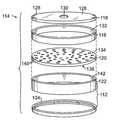
- a process kit 114comprising several components 112 is provided to contain the energized gas into the cleaning chamber 24 and distribute the gas across the substrate surface as shown in FIGS. 4A and 4B .
- the components 112 of the process kit 114can include, for example, a top plate 116 , a top liner 118 , a gas distributor plate 120 , a bottom liner 122 , and a focus ring 124 .
- the components 112 of the process kit 114can be easily removed from the chamber 24 , for example, to replace or repair eroded components, or to adapt the cleaning chamber 24 for processing substrates 22 of different sizes.
- the process kit 114 componentscan be made from quartz because quartz is effective at reducing the recombination rate of process gas radicals such as hydrogen radicals.
- the top plate 116comprises an annular disk 126 having an outer peripheral edge 128 and an orifice 130 for passing process gas therethrough as illustrated in FIG. 4A .
- the top plate 116is sized to fit into the substrate cleaning chamber 24 and the orifice 130 has a diameter of between about 40 mm and about 45 mm and is located about the center of the top plate 116 such that the orifice 130 substantially overlaps with the gas inlet channel 40 of the upper chamber wall 32 .
- the top plate 116contacts the upper wall 32 of the chamber 24 .
- the top plate 116contacts and is supported by the top liner 118 .
- the top plate 116comprises a thickness of from about 1 mm to about 10 mm.
- the top liner 118contacts the outer peripheral edge 128 of the top plate 116 .
- the top liner 118comprises a cylinder that serves to confine the energized process gas and to protect the walls 30 of the cleaning chamber 24 from the energized process gas.
- the liner 118comprises a thickness of from about 0.60 cm to about 0.70 cm.
- the outer peripheral edge 128 of the top plate 116rests on the upper edge 132 of the top liner 118 .
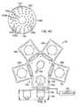
- a gas distributor plate 120has a top surface 134 contacting the top liner 118 , a bottom surface 136 , and a plurality of holes 140 therethrough for distributing process gas in the chamber 24 .
- the holes 140are shaped, sized, and distributed in a spaced apart relationship across the surface of the plate 120 to promote uniform delivery of the process gas to the surface of the substrate 22 .
- the plurality of holes 140comprises four rings 139 a - d of holes 140 a - d that are each sized with different diameters as shown in FIG. 4C .
- the innermost first ring 139 a of first holes 140 athat are sized with a diameter d.
- a second ring 139 b of second holes 140 b that each have a diameter 2d,are located radially outward of the first ring 139 a .
- a third ring 139 c of third holes 140 c that each have a diameter 3dare radially outward of the second ring 139 b .
- a fourth ring 139 d of fourth holes 140 d that each have a diameter 4dare being radially outward of the third ring 139 c .
- Such a distribution of holes 140 a - dprovides more uniform delivery of the process gas to the surface of the substrate 22 .
- the first holes 140 ahave a diameter d which is from about 1 to about 5 mm, and the other holes 140 b - d are sized accordingly.
- the first ring of holes 140 aeach have a diameter of from about 1 to about 5 mm
- the second ring of holes 140 beach have a diameter of from about 2 to about 10 mm
- the third ring of holes 140 ceach have a diameter of from about 3 to about 15 mm
- the fourth ring of holes 140 aeach have a diameter of from about 4 to about 20 mm.
- the different diameter holes 140 a - dare also spaced apart to include a larger number of holes on the fourth ring 139 d , and progressive smaller numbers of holes for the third ring 139 c , second ring 139 b , and first ring 139 a .
- the gas distributor plate 120can be composed of a ceramic, such as for example, aluminum oxide or silicon oxide, and the silicon oxide can be quartz.
- a bottom liner 122contacts the bottom surface 136 of the gas distributor plate 120 as shown in FIGS. 4A and 4B .
- the bottom liner 122also comprises a cylinder having an annular peripheral edge 142 that extends outward from the cylinder. The peripheral edge 142 contacts the bottom surface 136 of the gas distributor plate 120 and the sidewall 34 of the cleaning chamber 24 .
- a focus ring 124is provided to focus the energized process gas onto the substrate 22 .
- the focus ring 124comprises an inner flange 148 which rests on the peripheral edge of the support pedestal 80 and which has a sloped upper surface 150 joining a vertical surface 151 at the substrate periphery, as shown in FIGS. 3B and 4B .
- the sloped upper surface 150comprises an angle of between about 85 to about 100°, for example about 95°.
- the focus ring 124also has a foot 152 which is elevated about a outer ledge 154 of the substrate heating pedestal 80 .
- the process kit 114 components described abovecan comprise a filtering material, such as for example quartz, to adsorb ionic species from the energized gas to filter out the ionic species from the energized gas.
- a filtering materialsuch as for example quartz
- at least a portion of the surfaces of the top plate 116 , top liner 118 , gas distributor plate 120 , bottom liner 122 and focus ring 124comprises quartz, for example a coating of quartz.
- the quartzcan be deposited onto the surfaces of these process kit 114 components by physical vapor deposition or by hydrothermal deposition. A suitable thickness for a layer of quartz on these surfaces is from about 0.01 mm to about 4 mm.
- the process kit 114 components 112are composed of quartz.
- the quartz surfaces 74can be arranged to provide optimal filtering of the hydrogen ion species from the energized cleaning gas.
- the quartz surfaces 74comprise the interior surface of a portion of the ceramic liner 60 that connects the gas energizer zone 54 and the cleaning chamber 24 .
- the ceramic liner 60can comprise a quartz tube.
- the quartz surface 74comprises one or more surfaces of a gas distributor, such as for example the upper surface of the gas distributor plate 120 .
- the quartz surfacesmay also comprise a wire grid situated between the remote zone and the substrate, for example above the process zone, to further filter the activated cleaning gas.
- the temperature of the substrate 22is set to provide optimum conditions for the reduction of oxides in the deposits, and can even be set to accelerate the chemical reaction between the hydrogen-containing radicals and the deposits.
- the temperature of the substrate 22may be maintained at from about 0 to about 500° C., such as from about 150° C. to about 450° C., and even from about 25° C. to about 350° C., such as from about 150° C. to about 350° C.
- a bias power level applied to the substrate 22 during the cleaning processmay be desirably low, as a high bias power level can increase the bombardment of the substrate 22 by ions in the energized cleaning gas.
- a suitable bias power levelmay be less than about 100 Watts such as, for example, from about to about 0 to about 10 Watts, and even from about 1 to about 10 Watts, and may even be substantially zero.
- a higher bias power levelmay be applied to increase the rate of cleaning, such as a bias power level of greater than 100 Watts, and even from about 100 Watts to about 200 Watts.
- cleaning of the substrate 22can be improved by performing a heat treatment or annealing step to remove deposits from the substrate 22 .
- the substrate 22is heated to a temperature that is sufficiently high to vaporize material from the substrate 22 .
- a flow of a reducing gasmay also be provided during the heat treatment step to inhibit the formation of oxides on the substrate 22 .
- a suitable reducing gasmay comprise a hydrogen-containing gas, such as for example H 2 .
- the heat treatment stepcan be performed without substantially energizing the reducing gas, for example without substantially coupling RF or microwave energy to the reducing gas, to provide a relatively gentle initial clean of the substrate 22 prior to the energized hydrogen radical cleaning step.
- a cleaning gascomprising from about 50 to about 1000 sccm of H 2 , such as 300 sccm of H 2 , and from about 0 to about 10 sccm H 2 O, such as 3 sccm H 2 O is activated in the chamber 42 of the remote gas energizer 52 by applying a power level of from about 300 Watts to about 3000 Watts, such as 1050 Watts.
- the remote chamber 42 pressureis maintained at less than about 10 Torr, such as about 1 Torr.
- a bias power level of from about 0 to about 100 Watts, such as 50 Wattsis applied to bias the substrate 22 , and the temperature of the substrate 22 is maintained at from about 150 to about 450° C., such as 250° C.
- the cleaning processsubstantially removes the deposits to provide a cleaned surface.
- the pressure in the chamber 24is reduced to a pressure of less than about 10 mTorr, to evacuate spent cleaning gas and cleaning by-products and to reduce the likelihood of contamination of the multi-chamber apparatus 26 by the cleaning chamber 24 .
- the substrate 22can then be transferred under vacuum via a substrate transfer chamber having a transfer robot 119 to a deposition chamber 24 b to deposit a second metal-containing conductor 21 , such as at least one of copper, aluminum, tantalum, tungsten, tantalum nitride and tungsten nitride, on the freshly cleaned metal-containing conductor surface.
- a multi-chamber apparatus 20 suitable for processing substrates 22comprises one or more process chambers 28 a - d which can include the cleaning chamber 24 , as shown in FIG. 5 .
- the chambersare mounted on a platform that provides electrical, plumbing, and other support functions.
- the platformtypically supports a load lock 156 to receive a cassette 158 of substrates 22 to be processed and a substrate transfer chamber 154 containing a robot 162 to transfer substrates 22 from the cassette 158 to the different chambers 28 a - d for processing and return them after processing.
- the different chambers 28 a - dmay include, for example, a cleaning chamber 24 , a deposition chamber 28 b for depositing materials on wafers, optionally, a heat treatment chamber 28 c , and other processing chambers.
- one of the chamberscomprises the cleaning chamber 24 for removing deposits formed on a metal-containing conductor on the substrate 22 .
- the substrate 22can be transferred by the robot 162 to a deposition chamber 28 d to deposit material such as a metal-containing conductor on the cleaned substrate 22 .
- the substrate 22can also be transferred by the robot 162 to a second deposition chamber 28 c capable of depositing another material, such as another metal-containing conductor, over the first material deposited in the first chamber 28 b .
- the chambers 28 a - dare interconnected to form a continuous vacuum environment within the walls 164 of the substrate transfer chamber 154 to provide as process which may proceed uninterrupted and reducing contamination of substrates 22 .
- the transfer chamber 154comprises a wall 160 having an exhaust port 164 to exhaust gases and to maintain a low pressure environment, such as a pressure of less than about 10 mTorr, in order to reduce contamination of the chambers.
- the multi-chamber apparatus 26can be operated by a controller 170 via a hardware interface.
- the controller 170comprises a computer (not shown) having a central processor unit (CPU) that is coupled to a memory and peripheral computer components.
- the memorymay include a removable storage media, such as for example a CD or floppy drive, a non-removable storage media, such as for example a hard drive, and random access memory.
- the controller 170may further comprise a plurality of interface cards including, for example, analog and digital input and output boards, interface boards, and motor controller boards.
- the controller 170comprises a computer-readable program may be stored in the memory, for example on the non-removable storage media or on the removable storage media.
- the computer readable programgenerally comprises process control software comprising program code to operate the chambers 28 a - d and their components, the transfer chamber 154 and robot 162 , process monitoring software to monitor the processes being performed in the chambers, safety systems software, and other control software, as for example.
- the computer-readable programmay be written in any conventional computer-readable programming language.
- the chamber 24may comprise components other than those specifically described, as would be apparent to those of ordinary skill in the art.
- the terms below, above, bottom, top, up, down, first and second and other relative or positional termsare shown with respect to the exemplary embodiments in the figures and are interchangeable. Therefore, the appended claims should not be limited to the descriptions of the preferred versions, materials, or spatial arrangements described herein to illustrate the invention.
Landscapes
- Engineering & Computer Science (AREA)
- Physics & Mathematics (AREA)
- Plasma & Fusion (AREA)
- Chemical & Material Sciences (AREA)
- Analytical Chemistry (AREA)
- Condensed Matter Physics & Semiconductors (AREA)
- Microelectronics & Electronic Packaging (AREA)
- Power Engineering (AREA)
- Computer Hardware Design (AREA)
- General Physics & Mathematics (AREA)
- Manufacturing & Machinery (AREA)
- Health & Medical Sciences (AREA)
- Epidemiology (AREA)
- Public Health (AREA)
- Drying Of Semiconductors (AREA)
- Cleaning Or Drying Semiconductors (AREA)
- Physical Or Chemical Processes And Apparatus (AREA)
- Container, Conveyance, Adherence, Positioning, Of Wafer (AREA)
- Cleaning In General (AREA)
Abstract
Description
This application is filed as a non-provisional application and claims priority from provisional application No. 60/940,959 which was filed on May 30, 2007, and which is incorporated by reference herein in its entirety.
In the processing of substrates such as semiconductors and displays, layers are formed on the substrate, and then etched to form features such as electrically conducting interconnects, contacts, vias, gates and barriers. For example, a pattern of electrical interconnect lines can be made by depositing a metal-containing conductor on the substrate, forming a patterned etch resistant material on the conductor, etching the conductor to form the interconnect lines, removing remnant resist, and depositing dielectric over the etched features. The dielectric layer can be further etched to form contact holes or vias that expose the underlying metal-containing conductor material or other substrate layers. Electrically conducting material is then deposited into the etched holes or trenches to electrically contact the underlying conductor. For example, in the formation of copper-containing interconnects, the dielectric layer can be etched to form contact holes that expose an underlying copper conductor material. A thin seed layer of copper can be deposited over the exposed conductor and contact hole to facilitate subsequent copper electroplating processes to fill the contact holes.
However, contaminants and undesirable surface material on the metal-containing conductor require cleaning of the exposed conductor surfaces before subsequent process steps are performed. For example, a native oxide film often forms on a conductor exposed to oxygen species during an intermediate process step, for example, during a resist stripping process in which an oxygen-containing gas plasma is used to strip resist, or when transferring the substrate between different chambers. The oxide films increase the electrical resistance at the contact interface between conductor surfaces. The surface material can also have residual process deposits from previous processes, such as for example carbon-containing, silicon-containing, fluorine-containing, and nitrogen-containing process residues. These process deposits can cause voids or other irregularities to form at the interface between the exposed and deposited materials.
Substrate cleaning chambers, also known as pre-clean chambers, are used to clean oxide films and other undesirable process deposits from the substrate surface prior to processing and in between processing steps. During the cleaning process, the substrate is supported in the cleaning chamber and an energized cleaning gas is formed in a remote gas chamber and introduced into the chamber. The cleaning gas reacts with and remove the surface residues. In some processes, the substrate heating pedestal includes a heating element to control the temperature of the substrate during cleaning.
However, one problem with the use of an energized cleaning gas in such cleaning processes is that it is difficult to control the energy of the radical and ionic species of the excited cleaning gas. Higher energy collisions between the cleaning gas and the substrate surface can cause damage to the underlying substrate. Lighter ions in the cleaning gas, such as for example H+ can also be detrimental when they penetrate the surface of the substrate to damage underlying dielectric layers. Thus, it is desirable to control the energy of, and type of energized species introduced into the process chamber.
Another problem is that the cleaning gas often etches away and erodes the remote chamber wall 'surrounding the excitation region of the remote within a gas energizer, and can even etch and erode components inside the cleaning chamber. Such erosion damages these components, and if the component is an integral part of the chamber, the chamber must be shut down to allow the component to be refurbished or replaced after a predetermined number of process cycles, which is undesirable. Conventional stainless steel walls and liners are particularly susceptible to erosion and require frequent replacement or refurbishment.
Yet another problem occurs when the substrate heating pedestal in the cleaning chamber that contacts the substrate, transfers contaminants and process residues deposits to the backside of the substrate or even scratches the substrate during the substrate transferring process. Substrate heating pedestals containing heating elements can also provide non-uniform heating across the surface of the substrate. Substrate heating pedestals having a substrate receiving surface made up of raised mesas and grooves allow flow of a heat transfer gas behind the substrate to improve temperature uniformity but still transfer undesirable amounts of process residues and deposits to the substrate.
Thus, it is desirable to have a cleaning chamber and gas energizer that can selectively filter energized gas species, for example, to filter out certain ionic species from the cleaning gas. It is also desirable to have chamber components that can be easily replaced or refurbished. It is further desirable to have a substrate heating pedestal that minimizes contamination of the substrate by the transfer of process deposits to the backside surface of the substrate. It is also desirable to have a substrate heating pedestal that allows a more uniform heating of the substrate.
These features, aspects, and advantages of the present invention will become better understood with regard to the following description, appended claims, and accompanying drawings, which illustrate examples of the invention. However, it is to be understood that each of the features can be used in the invention in general, not merely in the context of particular drawings, and the invention includes any combination of these features, where:
An embodiment of ansubstrate apparatus 20 comprising acleaning chamber 24 suitable for cleaning asubstrate 22, is shown in itsFIG. 1 . Thecleaning chamber 24, as shown, is suitable forcleaning substrates 22 such as semiconductor wafers; however, thecleaning chamber 24 can be adapted by those of ordinary skill to cleanother substrates 22, such as flat panel displays, polymer panels, or other electrical circuit receiving structures. Thus, the scope of the present invention should not be limited to the illustrative embodiments of the cleaning chamber shown herein. Generally, thecleaning chamber 24 comprises one ormore enclosure walls 30, which can include anupper wall 32,sidewalls 34, and abottom wall 36, and which enclose aprocess zone 38. Energized cleaning gas is provided to agas inlet channel 40 of thecleaning chamber 24 from aremote chamber 42. The cleaning gas reacts with thesubstrate 22 and other surfaces within thechamber 24. Spent gas and byproducts are exhausted from thechamber 24 through anexhaust system 44 which may include anexhaust port 46 that receives gas from theprocess zone 38, and can also include athrottle valve 48 to control the pressure of gas in thechamber 24, and one ormore exhaust pumps 50, such as a turbo-molecular exhaust pump. Theexhaust system 44 can be capable of maintaining a sub-atmospheric pressure in thechamber 24.
Aremote chamber 42 suitable for remotely energizing the cleaning gas comprises aremote gas energizer 52 which couples energy to agas energizer zone 54. Acleaning gas source 56 provides a cleaning gas to thegas energizer zone 54. Aflow valve 58 can be provided to control a flow rate of the cleaning gas into theremote chamber 42. Thegas energizer 52 couples energy to the cleaning gas in thegas energizer zone 54 to form an energized cleaning gas comprising ionic and radical species. Thegas energizer 52 can couple, for example, RF or microwave energy to the cleaning gas. In one version, theremote gas energizer 52 comprises aninductor antenna 57 that inductively couples RF energy to the cleaning gas in thegas energizer zone 54 at a power level of, for example, from about 100 Watts to about 10 kWatts. Thegas energizer 52 can also be a toroidal gas energizer to couple energy to the cleaning gas in theremote zone 54, as for example described in U.S. Pat. No. 6,150,628 to Smith et al., which is incorporated by reference herein and in its entirety. A suitable RF power level applied by the toroidal gas energizer may be from about 1000 Watts to about 10,000 Watts. Aremote gas energizer 52 comprising a microwave gas activator providing a microwave power level of from about 300 Watts to about 5 kW, can also be used.
A consumableceramic liner 60 connects agas outlet channel 62 of theremote gas energizer 52 to agas inlet channel 40 of thechamber 24, as shown inFIGS. 2A and 2B . Theliner 60 serves to protect thechannels liner 60, such that theinner surface 61 of theliner 60 is exposed to the energized gas species. Theliner 60 comprises aninlet cylinder 64 having an outer diameter sized to fit in thegas outlet channel 62 of the remote gas energizer. In one version, theinlet cylinder 64 has a length L that is sufficiently long to extend out from theremote chamber 42 by a distance of at least about 50 mm. The length L is sufficiently short to terminate at least about 1 mm before the end of thegas inlet 40 of thechamber 24. In one version, theinlet cylinder 64 has a length L of from about 100 to about 110 mm, and a diameter of between about 1 cm to about 4 cm.
Aconical flare 66 joins theinlet cylinder 64 to anoutlet cylinder 68. Theconical flare 66 comprises a tube having a diameter that increases along a conical surface over the length of theflare 66. Theconical flare 66 has anupper end 70 and alower end 72. The outer diameter of theupper end 70 of theconical flare 66 is sized to correspond to the outer diameter of theinlet cylinder 64 at the junction between theconical flare 66 and theinlet cylinder 64. The outer diameter of thelower end 72 of theconical flare 66 is sized to correspond to the outer diameter of theoutlet cylinder 68 at the junction between theconical flare 66 and theoutlet cylinder 68. The diameter of thelower end 72 of theconical flare 66 is larger than the diameter of theupper end 70 of theconical flare 66 by at least a factor of 1.5. In one version theinlet cylinder 64, theconical flare 66 and theoutlet cylinder 68 are integrally connected.
Theconical flare 66 serves to gradually increase the diameter of the inner volume of theliner 60 between the upper and lower ends70,72 to provide a more uniform distribution of energized gas species entering the process chamber. An abrupt change in diameter was believed to result in non-uniform gas distribution from the outlet of the liner. Theconical flare 66 gradually tapers the diameter from the first diameter of theinlet cylinder 64 to the second diameter of theoutlet cylinder 68 to provide a gradual increase in volume along the flow path of the dissociated gas species. In one version, theconical flare 66 comprises a conical surface that is angled relative to a vertical axis passing through the centerline of the conical flare, at an angle of from about 10 degrees to about 60 degrees. Also, the ratio of the length of theconical flare 66 to the length of theoutlet cylinder 68 is from about 1:2 to about 1.8. Spacing the increase in volume across a length of theconical flare 66 provides better distribution of gas species at the outlet end72 of theconical flare 66.
Theliner 60 also has anoutlet cylinder 68 that is connected to thegas inlet channel 40 of thesubstrate cleaning chamber 24. In one version, theoutlet cylinder 68 has an outer diameter sized to fit in thegas inlet channel 40 of thesubstrate cleaning chamber 24. Theoutlet cylinder 68 has a length L that is sufficiently short to terminate before a process zone of the cleaningchamber 24 to avoid erosion in the chamber environment. When theinlet cylinder 64 has a first diameter, theoutlet cylinder 68 comprises a second diameter that is at least 1.5 times larger that the first diameter. In one version, theoutlet cylinder 68 has a diameter of from about 2 cm to about 8 cm or more typically about 4 cm. Theoutlet cylinder 68 protects the inner surfaces of thegas inlet 40 of the chamber from erosion by the energized gas species, while also increasing the diameter of the liner to reduce collisions between the energized gas species formed in theremote zone 54.
Theconsumable liner 60 comprises a ceramic material capable of scavenging an ion species from the energized gas generated in the remote gas energizer. For example, theliner 60 can comprise quartz, aluminum oxide or aluminum nitride. In one version, theliner 60 comprises quartz and is capable of scavenging hydrogen ions from the energized gas by adsorbing some of the hydrogen ions onto itsinner surface 74. The quartzinner surface 74 is believed to act as an ion filter76 to reduce the recombination of the radicals by providing a surface to which hydrogen-containing species can adsorb. It is also believed that hydrogen-containing species that impinge on thequartz surface 74 release an adsorbed hydrogen-containing radical into the energized gas thereby regenerating free hydrogen radicals. However, hydrogen ions are not regenerated by the quartz surfaces74, and thus, the hydrogen ions impinging on the quartz surface recombine to form electrically neutral, non-ionic species. Thus, passing the activated or energized cleaning gas over thequartz surface 74, causes ionic species to be filtered out from the energized cleaning gas while hydrogen radicals are preserved.
The thickness of theconsumable liner 60 is selected depending upon the number of process cycles the liner must withstand before replacement. The energized gas is capable of etching and eroding theliner 60, thus, theliner 60 must be replaced after a predetermined number of process cycles. Also, the adsorption properties of theliner 60 degrade as more and more ions are adsorbed onto the surface of the ceramic liner. The number of cycles that theliner 60 can withstand is related to the thickness of theliner 60. In one version, theliner 60 is sufficiently thick to scavenge ion species for at least about 30,000 process cycles, and has a thickness of from about 2 mm to about 6 mm.
Theliner 60 can be made by molding a ceramic powder into the desired shape, for example, by cold isostatic pressing. For example, ceramic powder is combined with a liquid binding agent such as the organic binding agent polyvinyl alcohol. The mixture is placed in a rubber bag of an isostatic pressing device and a pressure is uniformly applied on the walls of the bag to compact the mixture to form a ceramic structure having the desired tubular shape. The pressure can be applied, for example, by immersing the flexible container in water or by other pressurizing methods. The molded ceramic preform can be made cylindrical or ring-like using a hollow tube mold, and the resultant molded ceramic preform can be further shaped by machining. The shaped ceramic preform is then sintered to form a sintered ceramic. For example, aluminum oxide can be sintered at a temperature of from about 1300° C. to about 1800° C. for about 48 to about 96 hours, typically at a pressure of about 1 atm. The sintered ceramic material can be further shaped, for example, by machining, polishing, laser drilling, or using other methods, to provide the desired ceramic structure.
Theliner 60 is held in place in the chamber by aliner locking cylinder 71. Theliner locking cylinder 71 is sized to slide over the outer diameter of theoutlet cylinder 68 of theliner 60 and it rests against anannular lip 69 of theoutlet cylinder 68. as shown inFIGS. 2A and 2B . Theliner locking cylinder 71 fits in between theouter cylinder 68 of theliner 60 and theaperture wall 73 to form a gas tight seal as shown inFIG. 1 , and can b made from a metal or ceramic material.
Advantageously, theliner locking cylinder 71 facilitates placement into theupper chamber wall 32, and also facilitates removal of theliner 60 after it is exposed to plasma for a preset number of process cycles, for refurbishment or replacement. Theliner locking cylinder 71 comprises acircular flange 73 which extends out from one end of the lockingcylinder 71. Thecircular flange 73 has a flat key75 which is inserted into a matching flatkey portion 77 on anannular lip 79 extending out from theupper chamber wall 32, as shown inFIG. 2B . Twisting theliner locking cylinder 71 rotates thecircular flange 73 so that it slides behind theannular lip 79 of theupper chamber wall 32 to lock the circular flange behind the same. A locking blocker (not shown) such as a locking pin can be inserted into the pathway of the rotatingcircular flange 73 to block and stop the flange from further rotation.
A method of inserting theliner 60 into a chamber lid for connecting agas outlet channel 62 of aremote chamber 42 to agas inlet channel 40 of acleaning chamber 24 is also demonstrated inFIG. 2B . In this method, theliner locking cylinder 71 is first placed over theoutlet cylinder 68 of theceramic liner 60. Then, aliner holding tool 81 is passed into theoutlet cylinder 68 of theceramic liner 60 so that the outer diameter of theliner holding tool 81 grips the inner diameter of theoutlet cylinder 68. A user grasps theliner holding tool 81 and then inserts theinlet cylinder 64 of theceramic liner 60 into thegas outlet channel 62 of theremote chamber 42. Theliner holding tool 81 is then twisted to lock thecircular flange 73 of theliner locking cylinder 71 into a matchingannular lip 79 of theupper chamber wall 32 as described.
Thechamber 24 may also optionally comprise a chamber gas energizer (not shown) that couples energy to the gas in theprocess zone 38 of thechamber 24. For example, the chamber gas energizer can comprise one or more of electrodes and an inductor antenna to couple RF energy.
Asubstrate heating pedestal 80 is provided to hold thesubstrate 22 in theprocess zone 38 of thesubstrate cleaning chamber 24 as shown inFIGS. 1 ,3A,3B and4B. Thepedestal 80 comprises anannular plate 82 having asubstrate receiving surface 84 with an array ofrecesses 88 and aheating element 92 embedded in theannular plate 82. Theheating element 92 is controlled by acontroller 78. Thecontroller 78 is able to supply a variable power level to theheating element 92 in response to at least one of: input from one ormore detectors 106 that monitor the conditions in thecleaning chamber 24 or theremote chamber 42, or input from a user of theapparatus 20. Thepedestal 80 can optionally comprise an electrode (not shown) that can be electrically biased to hold thesubstrate 22 to thepedestal 80 or affect the characteristics of the process, such as the degree of ion bombardment of thesubstrate 22. The bias applied to the electrode is also controlled by thecontroller 78.
A plurality ofceramic balls 90 are each positioned in arecess 88 on thesubstrate receiving surface 84 as shown inFIG. 3A . Theceramic balls 90 are embedded in thesurface 84 of thepedestal 80 such that a portion of the surface of eachball 90 is situated above the plane of thepedestal surface 84. As such, atop region 144 of theballs 90 make up a raisedsubstrate receiving surface 86 consisting of N discrete regions, where N is the number ofballs 90 embedded in thesurface 84 of thepedestal 80. The raisedsubstrate receiving surface 86 is vertically separated from thepedestal surface 84. That is, the raisedsubstrate receiving surface 86 is higher than the surface of theannular plate 82 by from about 0.01 mm to about 0.5 mm. Supporting thesubstrate 22 by a series of discrete points, and at a vertical distance from the surface of theannular plate 82 of theheating pedestal 80 allows for gas in thechamber 24 to transfer heat between thesubstrate 22 and the surface of theannular plate 82 during heating. Suspension of thesubstrate 22 above the surface of theannular plate 82 allows for a more uniform heating of thesubstrate 22, as compared to contacting thesubstrate 22 to the surface of theannular plate 82, because the thermal contact is not directly affected by local variations in the thermal conductivity and surface contact characteristics of theplate 82.
In one version, theceramic balls 90 are spherical in shape and the diameter of theballs 90 is sufficiently high to maintain the substrate receiving surface higher than the top surface of the annular plate by from about 0.01 mm to about 0.5 mm. Typically, theballs 90 comprise a diameter of between about 1 mm and about 3 mm. In one version, the spherical bodies have a diameter of about 2 mm and protrude from the upper surface of theannular plate 82 by about 0.04 mm. Theceramic balls 90 comprise at least one of silicon nitride, zirconium oxide, sapphire, synthetic corundum, and alumina oxide and in one version comprise alumina oxide.
Theannular plate 82 is constructed from twodisks FIGS. 3A and 3B , theannular plate 82 comprises afirst disk 94 having the raisedsubstrate receiving surface 86. Thefirst disk 94 comprises a thickness of from about 10 mm to about 30 mm and diameter of from about 10 cm to about 70 cm. The diameter of thedisk 94 is dependant on the dimensions of the substrate to be processed. The receiving surface of thedisk 94 comprises a plurality ofrecesses 88 each having a diameter and a depth sufficient to receive aceramic ball 90. Therecesses 88 can be formed by machining and preferably comprise sides which are sloped inward by between about 2 and about 20 degrees such that the diameter of therecess 88 at the surface of the first disk is slightly less than the diameter of theceramic ball 90.Recesses 88 machined in this manner are capable of confining the insertedceramic balls 90 to the surface of theannular plate 82 after insertion.
Asecond disk 96 is provided having a diameter to match the diameter of thefirst disk 94 and a thickness of between about 6 mm and about 15 mm. Thesecond disk 96 comprises achannel 98 shaped to receive theheating element 92 and is made of at least one of aluminum, copper, titanium, molybdenum or stainless steel, or combinations thereof. In one version, the second disk comprises aluminum, and the brazing bond material comprises an aluminum brazing material. Theheating element 92 comprises a resistor assembly having sufficient electrical resistance to maintain thesurface 84 of theannular plate 82 at temperatures of from about room temperature to about 400° C. Theheating element 92 is powered viaterminal posts 100 which extend through thesecond disk 96 about thecenter 102 of the disk.
Theannular plate 82 with embeddedheating element 92 may be formed by machining afirst disk 94 from an aluminum sheet having a thickness of about 5 mm.Recesses 88 having a depth of about 2 mm from thesurface 84 of thefirst disk 94 are drilled into thesurface 84 of thedisk 94 corresponding to the desired placement of the countersunkceramic balls 90. Asecond disk 96 is machined to have the same diameter as thefirst disk 94 from an aluminum sheet having a thickness of from about 11.5 mm to about 12.5 mm. Aserpentine channel 98 is machined in thedisk 96, thechannel 98 having a width and depth corresponding to the dimensions of theheating element 92. At least one pair of holes (not shown) are drilled about thecenter 102 of thesecond disk 96. The drilled holes have a diameter of at least 10% greater than the diameter of theterminals 100 of theheating element 92. Theheating element 92 is applied to the grooved side of thesecond disk 96 by pressing it into thechannel 98 and threading theterminals 100 through the drilled holes. A brazing foil or brazing compound is placed onto the grooved surface of thesecond disk 96 such that it covers the surface of thesecond disk 96. The non-pitted side of thefirst disk 94 is held onto the brazing surface and the assembly is aligned such that the circumferences of the first andsecond disks bond 104.
The backside surface of theannular plate 82 is mounted to asupport post 110 used for supporting theannular plate 82. Thesupport post 110 comprises a rod having a receiving surface adapted to receive the backside surface of theannular plate 82. The rod may comprise a metal such as stainless steel or aluminum and may be a solid or a hollow structure. In one version, thesupport post 110 also comprises a bellows and a lift mechanism (not shown) that is adapted to raise and lower thepedestal 80 into position for receiving asubstrate 22, treating thesubstrate 22 and removing thesubstrate 22 from thechamber 24. The method of fastening theannular plate 82 to thesupport post 110 can comprise welding thesupport post 110 to the bottom surface of theannular plate 82, welding a threaded adapter to the bottom surface of theannular plate 82 and then screwing theannular plate 82 to thesupport post 110 or by welding a hollowed tube onto the bottom surface of theannular plate 82 and then clamping the hollowed tube to thesupport post 110.
Aprocess kit 114 comprisingseveral components 112 is provided to contain the energized gas into the cleaningchamber 24 and distribute the gas across the substrate surface as shown inFIGS. 4A and 4B . Thecomponents 112 of theprocess kit 114 can include, for example, atop plate 116, atop liner 118, agas distributor plate 120, abottom liner 122, and afocus ring 124. Thecomponents 112 of theprocess kit 114 can be easily removed from thechamber 24, for example, to replace or repair eroded components, or to adapt thecleaning chamber 24 forprocessing substrates 22 of different sizes. Theprocess kit 114 components can be made from quartz because quartz is effective at reducing the recombination rate of process gas radicals such as hydrogen radicals.
Thetop plate 116 comprises anannular disk 126 having an outerperipheral edge 128 and anorifice 130 for passing process gas therethrough as illustrated inFIG. 4A . Thetop plate 116 is sized to fit into thesubstrate cleaning chamber 24 and theorifice 130 has a diameter of between about 40 mm and about 45 mm and is located about the center of thetop plate 116 such that theorifice 130 substantially overlaps with thegas inlet channel 40 of theupper chamber wall 32. Thetop plate 116 contacts theupper wall 32 of thechamber 24. Thetop plate 116 contacts and is supported by thetop liner 118. Thetop plate 116 comprises a thickness of from about 1 mm to about 10 mm.
Thetop liner 118 contacts the outerperipheral edge 128 of thetop plate 116. Thetop liner 118 comprises a cylinder that serves to confine the energized process gas and to protect thewalls 30 of the cleaningchamber 24 from the energized process gas. Theliner 118 comprises a thickness of from about 0.60 cm to about 0.70 cm. In one version, the outerperipheral edge 128 of thetop plate 116 rests on theupper edge 132 of thetop liner 118.
Agas distributor plate 120 has atop surface 134 contacting thetop liner 118, abottom surface 136, and a plurality ofholes 140 therethrough for distributing process gas in thechamber 24. Theholes 140 are shaped, sized, and distributed in a spaced apart relationship across the surface of theplate 120 to promote uniform delivery of the process gas to the surface of thesubstrate 22. In one version, the plurality ofholes 140 comprises four rings139a-dofholes 140a-dthat are each sized with different diameters as shown inFIG. 4C . In one version, the innermost first ring139aoffirst holes 140athat are sized with a diameter d. A second ring139bofsecond holes 140bthat each have a diameter 2d, are located radially outward of the first ring139a. Athird ring 139cofthird holes 140cthat each have a diameter 3d are radially outward of the second ring139b. Afourth ring 139doffourth holes 140dthat each have a diameter 4d are being radially outward of thethird ring 139c. Such a distribution ofholes 140a-dprovides more uniform delivery of the process gas to the surface of thesubstrate 22. In one version, thefirst holes 140ahave a diameter d which is from about 1 to about 5 mm, and theother holes 140b-dare sized accordingly. As one example, the first ring ofholes 140aeach have a diameter of from about 1 to about 5 mm; the second ring ofholes 140beach have a diameter of from about 2 to about 10 mm; the third ring ofholes 140ceach have a diameter of from about 3 to about 15 mm; and the fourth ring ofholes 140aeach have a diameter of from about 4 to about 20 mm. In one version, thedifferent diameter holes 140a-dare also spaced apart to include a larger number of holes on thefourth ring 139d, and progressive smaller numbers of holes for thethird ring 139c, second ring139b, and first ring139a. Thegas distributor plate 120 can be composed of a ceramic, such as for example, aluminum oxide or silicon oxide, and the silicon oxide can be quartz.
Abottom liner 122 contacts thebottom surface 136 of thegas distributor plate 120 as shown inFIGS. 4A and 4B . Thebottom liner 122 also comprises a cylinder having an annularperipheral edge 142 that extends outward from the cylinder. Theperipheral edge 142 contacts thebottom surface 136 of thegas distributor plate 120 and thesidewall 34 of the cleaningchamber 24.
Afocus ring 124 is provided to focus the energized process gas onto thesubstrate 22. Thefocus ring 124 comprises aninner flange 148 which rests on the peripheral edge of thesupport pedestal 80 and which has a slopedupper surface 150 joining avertical surface 151 at the substrate periphery, as shown inFIGS. 3B and 4B . The slopedupper surface 150 comprises an angle of between about 85 to about 100°, for example about 95°. Thefocus ring 124 also has afoot 152 which is elevated about aouter ledge 154 of thesubstrate heating pedestal 80.
Theprocess kit 114 components described above can comprise a filtering material, such as for example quartz, to adsorb ionic species from the energized gas to filter out the ionic species from the energized gas. In one version, at least a portion of the surfaces of thetop plate 116,top liner 118,gas distributor plate 120,bottom liner 122 andfocus ring 124 comprises quartz, for example a coating of quartz. The quartz can be deposited onto the surfaces of theseprocess kit 114 components by physical vapor deposition or by hydrothermal deposition. A suitable thickness for a layer of quartz on these surfaces is from about 0.01 mm to about 4 mm. In one version, theprocess kit 114components 112 are composed of quartz.
The quartz surfaces74 can be arranged to provide optimal filtering of the hydrogen ion species from the energized cleaning gas. In one version, the quartz surfaces74 comprise the interior surface of a portion of theceramic liner 60 that connects thegas energizer zone 54 and thecleaning chamber 24. For example, theceramic liner 60 can comprise a quartz tube. In another version, thequartz surface 74 comprises one or more surfaces of a gas distributor, such as for example the upper surface of thegas distributor plate 120. The quartz surfaces may also comprise a wire grid situated between the remote zone and the substrate, for example above the process zone, to further filter the activated cleaning gas.
In one cleaning process performed in thecleaning chamber 24 ofapparatus 20, the temperature of thesubstrate 22 is set to provide optimum conditions for the reduction of oxides in the deposits, and can even be set to accelerate the chemical reaction between the hydrogen-containing radicals and the deposits. For example, the temperature of thesubstrate 22 may be maintained at from about 0 to about 500° C., such as from about 150° C. to about 450° C., and even from about 25° C. to about 350° C., such as from about 150° C. to about 350° C. In one version, a bias power level applied to thesubstrate 22 during the cleaning process may be desirably low, as a high bias power level can increase the bombardment of thesubstrate 22 by ions in the energized cleaning gas. A suitable bias power level may be less than about 100 Watts such as, for example, from about to about 0 to about 10 Watts, and even from about 1 to about 10 Watts, and may even be substantially zero. In another version, a higher bias power level may be applied to increase the rate of cleaning, such as a bias power level of greater than 100 Watts, and even from about 100 Watts to about 200 Watts.
It has further been discovered that cleaning of thesubstrate 22 can be improved by performing a heat treatment or annealing step to remove deposits from thesubstrate 22. In the heat treatment step, thesubstrate 22 is heated to a temperature that is sufficiently high to vaporize material from thesubstrate 22. A flow of a reducing gas may also be provided during the heat treatment step to inhibit the formation of oxides on thesubstrate 22. A suitable reducing gas may comprise a hydrogen-containing gas, such as for example H2. The heat treatment step can be performed without substantially energizing the reducing gas, for example without substantially coupling RF or microwave energy to the reducing gas, to provide a relatively gentle initial clean of thesubstrate 22 prior to the energized hydrogen radical cleaning step.
In one version of a suitable cleaning process, a cleaning gas comprising from about 50 to about 1000 sccm of H2, such as 300 sccm of H2, and from about 0 to about 10 sccm H2O, such as 3 sccm H2O is activated in thechamber 42 of theremote gas energizer 52 by applying a power level of from about 300 Watts to about 3000 Watts, such as 1050 Watts. Theremote chamber 42 pressure is maintained at less than about 10 Torr, such as about 1 Torr. A bias power level of from about 0 to about 100 Watts, such as 50 Watts is applied to bias thesubstrate 22, and the temperature of thesubstrate 22 is maintained at from about 150 to about 450° C., such as 250° C. The cleaning process substantially removes the deposits to provide a cleaned surface.
After the cleaning process has been completed, the pressure in thechamber 24 is reduced to a pressure of less than about 10 mTorr, to evacuate spent cleaning gas and cleaning by-products and to reduce the likelihood of contamination of the multi-chamber apparatus26 by the cleaningchamber 24. Thesubstrate 22 can then be transferred under vacuum via a substrate transfer chamber having a transfer robot119 to a deposition chamber24bto deposit a second metal-containing conductor21, such as at least one of copper, aluminum, tantalum, tungsten, tantalum nitride and tungsten nitride, on the freshly cleaned metal-containing conductor surface.
Amulti-chamber apparatus 20 suitable for processingsubstrates 22 comprises one or more process chambers28a-dwhich can include the cleaningchamber 24, as shown inFIG. 5 . The chambers are mounted on a platform that provides electrical, plumbing, and other support functions. The platform typically supports aload lock 156 to receive acassette 158 ofsubstrates 22 to be processed and asubstrate transfer chamber 154 containing arobot 162 to transfersubstrates 22 from thecassette 158 to the different chambers28a-dfor processing and return them after processing. The different chambers28a-dmay include, for example, a cleaningchamber 24, adeposition chamber 28bfor depositing materials on wafers, optionally, aheat treatment chamber 28c, and other processing chambers. For example, in one version, one of the chambers comprises the cleaningchamber 24 for removing deposits formed on a metal-containing conductor on thesubstrate 22. After the cleaning process is finished, thesubstrate 22 can be transferred by therobot 162 to adeposition chamber 28dto deposit material such as a metal-containing conductor on the cleanedsubstrate 22. Thesubstrate 22 can also be transferred by therobot 162 to asecond deposition chamber 28ccapable of depositing another material, such as another metal-containing conductor, over the first material deposited in thefirst chamber 28b. The chambers28a-dare interconnected to form a continuous vacuum environment within thewalls 164 of thesubstrate transfer chamber 154 to provide as process which may proceed uninterrupted and reducing contamination ofsubstrates 22. Thetransfer chamber 154 comprises awall 160 having anexhaust port 164 to exhaust gases and to maintain a low pressure environment, such as a pressure of less than about 10 mTorr, in order to reduce contamination of the chambers.
The multi-chamber apparatus26 can be operated by acontroller 170 via a hardware interface. Thecontroller 170 comprises a computer (not shown) having a central processor unit (CPU) that is coupled to a memory and peripheral computer components. Preferably, the memory may include a removable storage media, such as for example a CD or floppy drive, a non-removable storage media, such as for example a hard drive, and random access memory. Thecontroller 170 may further comprise a plurality of interface cards including, for example, analog and digital input and output boards, interface boards, and motor controller boards. In one version, thecontroller 170 comprises a computer-readable program may be stored in the memory, for example on the non-removable storage media or on the removable storage media. The computer readable program generally comprises process control software comprising program code to operate the chambers28a-dand their components, thetransfer chamber 154 androbot 162, process monitoring software to monitor the processes being performed in the chambers, safety systems software, and other control software, as for example. The computer-readable program may be written in any conventional computer-readable programming language.
Although exemplary embodiments of the present invention are shown and described, those of ordinary skill in the art may devise other embodiments which incorporate the present invention, and which are also within the scope of the present invention. For example, thechamber 24 may comprise components other than those specifically described, as would be apparent to those of ordinary skill in the art. Furthermore, the terms below, above, bottom, top, up, down, first and second and other relative or positional terms are shown with respect to the exemplary embodiments in the figures and are interchangeable. Therefore, the appended claims should not be limited to the descriptions of the preferred versions, materials, or spatial arrangements described herein to illustrate the invention.
Claims (22)
1. A gas distributor plate for a substrate process chamber, the gas distributor plate comprising:
(a) a first ring of first holes that each have a diameter d;
(b) a second ring of second holes that each have a diameter 2d, the second ring being radially outward of the first ring;
(c) a third ring of third holes that each have a diameter 3d, the third ring being radially outward of the second ring; and
(d) a fourth ring of fourth holes that each have a diameter 4d, the fourth ring being radially outward of the third ring.
2. A gas distributor plate according toclaim 1 wherein the diameter d is from about 1 to about 5 mm.
3. A gas distributor plate according toclaim 1 wherein the second holes have a diameter of from about 2 to about 10 mm.
4. A gas distributor plate according toclaim 1 wherein the third holes have a diameter of from about 3 to about 15 mm.
5. A gas distributor plate according toclaim 1 wherein the fourth holes have a diameter of from about 4 to about 20 mm.
6. A gas distributor plate according toclaim 1 composed of a ceramic.
7. A gas distributor plate according toclaim 6 wherein the ceramic comprises aluminum oxide or silicon oxide.
8. A gas distributor plate according toclaim 1 composed of quartz.
9. A gas distributor plate according toclaim 1 wherein the fourth ring comprises a larger number of holes than the third ring.
10. A gas distributor plate according toclaim 1 wherein the first ring or second ring comprises a smaller number of holes than the fourth ring.
11. A gas distributor plate for a substrate process chamber, the gas distributor plate comprising:
(a) a first ring of first holes that each have a diameter d of from about 1 to about 5 mm;
(b) a second ring of second holes that each have a diameter 2d of from about 2 to about 10 mm, the second ring being radially outward of the first ring;
(c) a third ring of third holes that each have a diameter 3d of from about 3 to about 15 mm, the third ring being radially outward of the second ring; and
(d) a fourth ring of fourth holes that each have a diameter 4d of from about 4 to about 20 mm, the fourth ring being radially outward of the third ring.
12. A gas distributor plate according toclaim 11 composed of a ceramic.
13. A gas distributor plate according toclaim 11 wherein the ceramic comprises aluminum oxide or silicon oxide.
14. A gas distributor plate according toclaim 11 composed of quartz.
15. A gas distributor plate according toclaim 11 wherein the fourth ring comprises a larger number of holes than the third ring.
16. A gas distributor plate according toclaim 11 wherein the first ring or second ring comprises a smaller number of holes than the fourth ring.
17. A gas distributor plate for a substrate process chamber, the gas distributor plate comprising:
(a) a first ring of first holes that each have a diameter of from about 1 to about 5 mm;
(b) a second ring of second holes that each have a diameter of from about 2 to about 10 mm, the second ring being radially outward of the first ring;
(c) a third ring of third holes that each have a diameter of from about 3 to about 15 mm, the third ring being radially outward of the second ring; and
(d) a fourth ring of fourth holes that each have a diameter of from about 4 to about 20 mm, the fourth ring being radially outward of the third ring.
18. A gas distributor plate according toclaim 17 composed of a ceramic.
19. A gas distributor plate according toclaim 17 wherein the ceramic comprises aluminum oxide or silicon oxide.
20. A gas distributor plate according toclaim 11 composed of quartz.
21. A gas distributor plate according toclaim 11 wherein the fourth ring comprises a larger number of holes than third ring.
22. A gas distributor plate according toclaim 11 wherein the first ring or second ring comprises a smaller number of holes than the fourth ring.
Priority Applications (13)
| Application Number | Priority Date | Filing Date | Title |
|---|---|---|---|
| US11/857,975US7942969B2 (en) | 2007-05-30 | 2007-09-19 | Substrate cleaning chamber and components |
| KR1020157004544AKR101593461B1 (en) | 2007-05-30 | 2008-05-27 | Substrate processing apparatus and components |
| PCT/US2008/006702WO2008153785A2 (en) | 2007-05-30 | 2008-05-27 | Substrate cleaning chamber and components |
| CN2008800179480ACN101730921B (en) | 2007-05-30 | 2008-05-27 | Substrate cleaning chamber and components |
| JP2010510311AJP5726521B2 (en) | 2007-05-30 | 2008-05-27 | Substrate cleaning chamber and components |
| KR1020097027534AKR101550579B1 (en) | 2007-05-30 | 2008-05-27 | Substrate cleaning chambers and parts |
| TW100133253ATWI474387B (en) | 2007-05-30 | 2008-05-28 | Substrate cleaning chamber and components |
| TW097119766ATWI359450B (en) | 2007-05-30 | 2008-05-28 | Substrate cleaning chamber and components |
| US13/109,917US8980045B2 (en) | 2007-05-30 | 2011-05-17 | Substrate cleaning chamber and components |
| JP2012261367AJP5844722B2 (en) | 2007-05-30 | 2012-11-29 | Substrate cleaning chamber and components |
| US14/613,219US20150144263A1 (en) | 2007-05-30 | 2015-02-03 | Substrate heating pedestal having ceramic balls |
| JP2015226713AJP2016076716A (en) | 2007-05-30 | 2015-11-19 | Substrate cleaning chamber and components |
| JP2017206061AJP2018050059A (en) | 2007-05-30 | 2017-10-25 | Substrate cleaning chamber and components |
Applications Claiming Priority (2)
| Application Number | Priority Date | Filing Date | Title |
|---|---|---|---|
| US94095907P | 2007-05-30 | 2007-05-30 | |
| US11/857,975US7942969B2 (en) | 2007-05-30 | 2007-09-19 | Substrate cleaning chamber and components |
Related Child Applications (1)
| Application Number | Title | Priority Date | Filing Date |
|---|---|---|---|
| US13/109,917DivisionUS8980045B2 (en) | 2007-05-30 | 2011-05-17 | Substrate cleaning chamber and components |
Publications (2)
| Publication Number | Publication Date |
|---|---|
| US20080295872A1 US20080295872A1 (en) | 2008-12-04 |
| US7942969B2true US7942969B2 (en) | 2011-05-17 |
Family
ID=40086776
Family Applications (3)
| Application Number | Title | Priority Date | Filing Date |
|---|---|---|---|
| US11/857,975Active2030-02-11US7942969B2 (en) | 2007-05-30 | 2007-09-19 | Substrate cleaning chamber and components |
| US13/109,917Active2028-11-17US8980045B2 (en) | 2007-05-30 | 2011-05-17 | Substrate cleaning chamber and components |
| US14/613,219AbandonedUS20150144263A1 (en) | 2007-05-30 | 2015-02-03 | Substrate heating pedestal having ceramic balls |
Family Applications After (2)
| Application Number | Title | Priority Date | Filing Date |
|---|---|---|---|
| US13/109,917Active2028-11-17US8980045B2 (en) | 2007-05-30 | 2011-05-17 | Substrate cleaning chamber and components |
| US14/613,219AbandonedUS20150144263A1 (en) | 2007-05-30 | 2015-02-03 | Substrate heating pedestal having ceramic balls |
Country Status (6)
| Country | Link |
|---|---|
| US (3) | US7942969B2 (en) |
| JP (4) | JP5726521B2 (en) |
| KR (2) | KR101593461B1 (en) |
| CN (1) | CN101730921B (en) |
| TW (2) | TWI474387B (en) |
| WO (1) | WO2008153785A2 (en) |
Cited By (369)
| Publication number | Priority date | Publication date | Assignee | Title |
|---|---|---|---|---|
| US20080311294A1 (en)* | 2007-06-15 | 2008-12-18 | Hideki Ito | Vapor-phase growth apparatus and vapor-phase growth method |
| US20120263875A1 (en)* | 2011-04-18 | 2012-10-18 | Siltronic Ag | Method and Apparatus For Depositing A Material Layer Originating From Process Gas On A Substrate Wafer |
| US20130014896A1 (en)* | 2011-07-15 | 2013-01-17 | Asm Japan K.K. | Wafer-Supporting Device and Method for Producing Same |
| US20130087099A1 (en)* | 2011-10-05 | 2013-04-11 | Applied Materials, Inc. | In-Situ Hydroxylation Apparatus |
| USD699692S1 (en)* | 2012-01-19 | 2014-02-18 | Applied Materials, Inc. | Upper liner |
| US20140060740A1 (en)* | 2012-08-30 | 2014-03-06 | Chang Gung University | Plasma processing device |
| US8822313B2 (en) | 2012-12-20 | 2014-09-02 | Intermolecular, Inc. | Surface treatment methods and systems for substrate processing |
| USD716239S1 (en)* | 2013-11-06 | 2014-10-28 | Applied Materials, Inc. | Upper chamber liner |
| USD716240S1 (en)* | 2013-11-07 | 2014-10-28 | Applied Materials, Inc. | Lower chamber liner |
| USD717746S1 (en)* | 2013-11-06 | 2014-11-18 | Applied Materials, Inc. | Lower chamber liner |
| US20140376897A1 (en)* | 2013-06-21 | 2014-12-25 | Applied Materials, Inc. | Light pipe window structure for thermal chamber applications and processes |
| US8960235B2 (en) | 2011-10-28 | 2015-02-24 | Applied Materials, Inc. | Gas dispersion apparatus |
| US20180053638A1 (en)* | 2016-08-16 | 2018-02-22 | Fei Company | Magnet used with a plasma cleaner |
| US10023960B2 (en) | 2012-09-12 | 2018-07-17 | Asm Ip Holdings B.V. | Process gas management for an inductively-coupled plasma deposition reactor |
| US10083836B2 (en) | 2015-07-24 | 2018-09-25 | Asm Ip Holding B.V. | Formation of boron-doped titanium metal films with high work function |
| US10134757B2 (en) | 2016-11-07 | 2018-11-20 | Asm Ip Holding B.V. | Method of processing a substrate and a device manufactured by using the method |
| US10229833B2 (en) | 2016-11-01 | 2019-03-12 | Asm Ip Holding B.V. | Methods for forming a transition metal nitride film on a substrate by atomic layer deposition and related semiconductor device structures |
| US10236177B1 (en) | 2017-08-22 | 2019-03-19 | ASM IP Holding B.V.. | Methods for depositing a doped germanium tin semiconductor and related semiconductor device structures |
| US10249577B2 (en) | 2016-05-17 | 2019-04-02 | Asm Ip Holding B.V. | Method of forming metal interconnection and method of fabricating semiconductor apparatus using the method |
| US10249524B2 (en) | 2017-08-09 | 2019-04-02 | Asm Ip Holding B.V. | Cassette holder assembly for a substrate cassette and holding member for use in such assembly |
| US10262859B2 (en) | 2016-03-24 | 2019-04-16 | Asm Ip Holding B.V. | Process for forming a film on a substrate using multi-port injection assemblies |
| US10269558B2 (en) | 2016-12-22 | 2019-04-23 | Asm Ip Holding B.V. | Method of forming a structure on a substrate |
| US10276355B2 (en) | 2015-03-12 | 2019-04-30 | Asm Ip Holding B.V. | Multi-zone reactor, system including the reactor, and method of using the same |
| US10283353B2 (en) | 2017-03-29 | 2019-05-07 | Asm Ip Holding B.V. | Method of reforming insulating film deposited on substrate with recess pattern |
| US10290508B1 (en) | 2017-12-05 | 2019-05-14 | Asm Ip Holding B.V. | Method for forming vertical spacers for spacer-defined patterning |
| US10312055B2 (en) | 2017-07-26 | 2019-06-04 | Asm Ip Holding B.V. | Method of depositing film by PEALD using negative bias |
| US10312129B2 (en) | 2015-09-29 | 2019-06-04 | Asm Ip Holding B.V. | Variable adjustment for precise matching of multiple chamber cavity housings |
| US10319588B2 (en) | 2017-10-10 | 2019-06-11 | Asm Ip Holding B.V. | Method for depositing a metal chalcogenide on a substrate by cyclical deposition |
| US10322384B2 (en) | 2015-11-09 | 2019-06-18 | Asm Ip Holding B.V. | Counter flow mixer for process chamber |
| US10340135B2 (en) | 2016-11-28 | 2019-07-02 | Asm Ip Holding B.V. | Method of topologically restricted plasma-enhanced cyclic deposition of silicon or metal nitride |
| US10340125B2 (en) | 2013-03-08 | 2019-07-02 | Asm Ip Holding B.V. | Pulsed remote plasma method and system |
| US10343920B2 (en) | 2016-03-18 | 2019-07-09 | Asm Ip Holding B.V. | Aligned carbon nanotubes |
| US10361201B2 (en) | 2013-09-27 | 2019-07-23 | Asm Ip Holding B.V. | Semiconductor structure and device formed using selective epitaxial process |
| US10367080B2 (en) | 2016-05-02 | 2019-07-30 | Asm Ip Holding B.V. | Method of forming a germanium oxynitride film |
| US10364496B2 (en) | 2011-06-27 | 2019-07-30 | Asm Ip Holding B.V. | Dual section module having shared and unshared mass flow controllers |
| US10366864B2 (en) | 2013-03-08 | 2019-07-30 | Asm Ip Holding B.V. | Method and system for in-situ formation of intermediate reactive species |
| US10381226B2 (en) | 2016-07-27 | 2019-08-13 | Asm Ip Holding B.V. | Method of processing substrate |
| US10381219B1 (en) | 2018-10-25 | 2019-08-13 | Asm Ip Holding B.V. | Methods for forming a silicon nitride film |
| US10378106B2 (en) | 2008-11-14 | 2019-08-13 | Asm Ip Holding B.V. | Method of forming insulation film by modified PEALD |
| US10388509B2 (en) | 2016-06-28 | 2019-08-20 | Asm Ip Holding B.V. | Formation of epitaxial layers via dislocation filtering |
| US10388513B1 (en) | 2018-07-03 | 2019-08-20 | Asm Ip Holding B.V. | Method for depositing silicon-free carbon-containing film as gap-fill layer by pulse plasma-assisted deposition |
| US10395919B2 (en) | 2016-07-28 | 2019-08-27 | Asm Ip Holding B.V. | Method and apparatus for filling a gap |
| US10403504B2 (en) | 2017-10-05 | 2019-09-03 | Asm Ip Holding B.V. | Method for selectively depositing a metallic film on a substrate |
| US10410943B2 (en) | 2016-10-13 | 2019-09-10 | Asm Ip Holding B.V. | Method for passivating a surface of a semiconductor and related systems |
| US10438965B2 (en) | 2014-12-22 | 2019-10-08 | Asm Ip Holding B.V. | Semiconductor device and manufacturing method thereof |
| US10435790B2 (en) | 2016-11-01 | 2019-10-08 | Asm Ip Holding B.V. | Method of subatmospheric plasma-enhanced ALD using capacitively coupled electrodes with narrow gap |
| US10446393B2 (en) | 2017-05-08 | 2019-10-15 | Asm Ip Holding B.V. | Methods for forming silicon-containing epitaxial layers and related semiconductor device structures |
| US10458018B2 (en) | 2015-06-26 | 2019-10-29 | Asm Ip Holding B.V. | Structures including metal carbide material, devices including the structures, and methods of forming same |
| US10468262B2 (en) | 2017-02-15 | 2019-11-05 | Asm Ip Holding B.V. | Methods for forming a metallic film on a substrate by a cyclical deposition and related semiconductor device structures |
| US10468251B2 (en) | 2016-02-19 | 2019-11-05 | Asm Ip Holding B.V. | Method for forming spacers using silicon nitride film for spacer-defined multiple patterning |
| US10480072B2 (en) | 2009-04-06 | 2019-11-19 | Asm Ip Holding B.V. | Semiconductor processing reactor and components thereof |
| US10483099B1 (en) | 2018-07-26 | 2019-11-19 | Asm Ip Holding B.V. | Method for forming thermally stable organosilicon polymer film |
| US10501866B2 (en) | 2016-03-09 | 2019-12-10 | Asm Ip Holding B.V. | Gas distribution apparatus for improved film uniformity in an epitaxial system |
| US10504742B2 (en) | 2017-05-31 | 2019-12-10 | Asm Ip Holding B.V. | Method of atomic layer etching using hydrogen plasma |
| US10510536B2 (en) | 2018-03-29 | 2019-12-17 | Asm Ip Holding B.V. | Method of depositing a co-doped polysilicon film on a surface of a substrate within a reaction chamber |
| US10529554B2 (en) | 2016-02-19 | 2020-01-07 | Asm Ip Holding B.V. | Method for forming silicon nitride film selectively on sidewalls or flat surfaces of trenches |
| US10529542B2 (en) | 2015-03-11 | 2020-01-07 | Asm Ip Holdings B.V. | Cross-flow reactor and method |
| US10529563B2 (en) | 2017-03-29 | 2020-01-07 | Asm Ip Holdings B.V. | Method for forming doped metal oxide films on a substrate by cyclical deposition and related semiconductor device structures |
| US10535516B2 (en) | 2018-02-01 | 2020-01-14 | Asm Ip Holdings B.V. | Method for depositing a semiconductor structure on a surface of a substrate and related semiconductor structures |
| US10541333B2 (en) | 2017-07-19 | 2020-01-21 | Asm Ip Holding B.V. | Method for depositing a group IV semiconductor and related semiconductor device structures |
| US10541173B2 (en) | 2016-07-08 | 2020-01-21 | Asm Ip Holding B.V. | Selective deposition method to form air gaps |
| US10559458B1 (en) | 2018-11-26 | 2020-02-11 | Asm Ip Holding B.V. | Method of forming oxynitride film |
| US10566223B2 (en) | 2012-08-28 | 2020-02-18 | Asm Ip Holdings B.V. | Systems and methods for dynamic semiconductor process scheduling |
| US10561975B2 (en) | 2014-10-07 | 2020-02-18 | Asm Ip Holdings B.V. | Variable conductance gas distribution apparatus and method |
| US10590535B2 (en) | 2017-07-26 | 2020-03-17 | Asm Ip Holdings B.V. | Chemical treatment, deposition and/or infiltration apparatus and method for using the same |
| US10600673B2 (en) | 2015-07-07 | 2020-03-24 | Asm Ip Holding B.V. | Magnetic susceptor to baseplate seal |
| US10607895B2 (en) | 2017-09-18 | 2020-03-31 | Asm Ip Holdings B.V. | Method for forming a semiconductor device structure comprising a gate fill metal |
| US10604847B2 (en) | 2014-03-18 | 2020-03-31 | Asm Ip Holding B.V. | Gas distribution system, reactor including the system, and methods of using the same |
| US10605530B2 (en) | 2017-07-26 | 2020-03-31 | Asm Ip Holding B.V. | Assembly of a liner and a flange for a vertical furnace as well as the liner and the vertical furnace |
| USD880437S1 (en) | 2018-02-01 | 2020-04-07 | Asm Ip Holding B.V. | Gas supply plate for semiconductor manufacturing apparatus |
| US10612136B2 (en) | 2018-06-29 | 2020-04-07 | ASM IP Holding, B.V. | Temperature-controlled flange and reactor system including same |
| US10612137B2 (en) | 2016-07-08 | 2020-04-07 | Asm Ip Holdings B.V. | Organic reactants for atomic layer deposition |
| US10643904B2 (en) | 2016-11-01 | 2020-05-05 | Asm Ip Holdings B.V. | Methods for forming a semiconductor device and related semiconductor device structures |
| US10643826B2 (en) | 2016-10-26 | 2020-05-05 | Asm Ip Holdings B.V. | Methods for thermally calibrating reaction chambers |
| US10658181B2 (en) | 2018-02-20 | 2020-05-19 | Asm Ip Holding B.V. | Method of spacer-defined direct patterning in semiconductor fabrication |
| US10658205B2 (en) | 2017-09-28 | 2020-05-19 | Asm Ip Holdings B.V. | Chemical dispensing apparatus and methods for dispensing a chemical to a reaction chamber |
| US10655221B2 (en) | 2017-02-09 | 2020-05-19 | Asm Ip Holding B.V. | Method for depositing oxide film by thermal ALD and PEALD |
| US10665452B2 (en) | 2016-05-02 | 2020-05-26 | Asm Ip Holdings B.V. | Source/drain performance through conformal solid state doping |
| US10685834B2 (en) | 2017-07-05 | 2020-06-16 | Asm Ip Holdings B.V. | Methods for forming a silicon germanium tin layer and related semiconductor device structures |
| US10683571B2 (en) | 2014-02-25 | 2020-06-16 | Asm Ip Holding B.V. | Gas supply manifold and method of supplying gases to chamber using same |
| US10692741B2 (en) | 2017-08-08 | 2020-06-23 | Asm Ip Holdings B.V. | Radiation shield |
| US10707106B2 (en) | 2011-06-06 | 2020-07-07 | Asm Ip Holding B.V. | High-throughput semiconductor-processing apparatus equipped with multiple dual-chamber modules |
| US10714315B2 (en) | 2012-10-12 | 2020-07-14 | Asm Ip Holdings B.V. | Semiconductor reaction chamber showerhead |
| US10714350B2 (en) | 2016-11-01 | 2020-07-14 | ASM IP Holdings, B.V. | Methods for forming a transition metal niobium nitride film on a substrate by atomic layer deposition and related semiconductor device structures |
| US10714385B2 (en) | 2016-07-19 | 2020-07-14 | Asm Ip Holding B.V. | Selective deposition of tungsten |
| US10714335B2 (en) | 2017-04-25 | 2020-07-14 | Asm Ip Holding B.V. | Method of depositing thin film and method of manufacturing semiconductor device |
| US10734244B2 (en) | 2017-11-16 | 2020-08-04 | Asm Ip Holding B.V. | Method of processing a substrate and a device manufactured by the same |
| US10731249B2 (en) | 2018-02-15 | 2020-08-04 | Asm Ip Holding B.V. | Method of forming a transition metal containing film on a substrate by a cyclical deposition process, a method for supplying a transition metal halide compound to a reaction chamber, and related vapor deposition apparatus |
| US10734497B2 (en) | 2017-07-18 | 2020-08-04 | Asm Ip Holding B.V. | Methods for forming a semiconductor device structure and related semiconductor device structures |
| US10741385B2 (en) | 2016-07-28 | 2020-08-11 | Asm Ip Holding B.V. | Method and apparatus for filling a gap |
| US10755922B2 (en) | 2018-07-03 | 2020-08-25 | Asm Ip Holding B.V. | Method for depositing silicon-free carbon-containing film as gap-fill layer by pulse plasma-assisted deposition |
| US10763141B2 (en)* | 2017-03-17 | 2020-09-01 | Applied Materials, Inc. | Non-contact temperature calibration tool for a substrate support and method of using the same |
| US10770286B2 (en) | 2017-05-08 | 2020-09-08 | Asm Ip Holdings B.V. | Methods for selectively forming a silicon nitride film on a substrate and related semiconductor device structures |
| US10767789B2 (en) | 2018-07-16 | 2020-09-08 | Asm Ip Holding B.V. | Diaphragm valves, valve components, and methods for forming valve components |
| US10770336B2 (en) | 2017-08-08 | 2020-09-08 | Asm Ip Holding B.V. | Substrate lift mechanism and reactor including same |
| US10787741B2 (en) | 2014-08-21 | 2020-09-29 | Asm Ip Holding B.V. | Method and system for in situ formation of gas-phase compounds |
| US10797133B2 (en) | 2018-06-21 | 2020-10-06 | Asm Ip Holding B.V. | Method for depositing a phosphorus doped silicon arsenide film and related semiconductor device structures |
| US10804098B2 (en) | 2009-08-14 | 2020-10-13 | Asm Ip Holding B.V. | Systems and methods for thin-film deposition of metal oxides using excited nitrogen-oxygen species |
| US10811256B2 (en) | 2018-10-16 | 2020-10-20 | Asm Ip Holding B.V. | Method for etching a carbon-containing feature |
| USD900036S1 (en) | 2017-08-24 | 2020-10-27 | Asm Ip Holding B.V. | Heater electrical connector and adapter |
| US10818758B2 (en) | 2018-11-16 | 2020-10-27 | Asm Ip Holding B.V. | Methods for forming a metal silicate film on a substrate in a reaction chamber and related semiconductor device structures |
| US10832903B2 (en) | 2011-10-28 | 2020-11-10 | Asm Ip Holding B.V. | Process feed management for semiconductor substrate processing |
| US10829852B2 (en) | 2018-08-16 | 2020-11-10 | Asm Ip Holding B.V. | Gas distribution device for a wafer processing apparatus |
| US10847371B2 (en) | 2018-03-27 | 2020-11-24 | Asm Ip Holding B.V. | Method of forming an electrode on a substrate and a semiconductor device structure including an electrode |
| US10847365B2 (en) | 2018-10-11 | 2020-11-24 | Asm Ip Holding B.V. | Method of forming conformal silicon carbide film by cyclic CVD |
| US10847366B2 (en) | 2018-11-16 | 2020-11-24 | Asm Ip Holding B.V. | Methods for depositing a transition metal chalcogenide film on a substrate by a cyclical deposition process |
| US10844484B2 (en) | 2017-09-22 | 2020-11-24 | Asm Ip Holding B.V. | Apparatus for dispensing a vapor phase reactant to a reaction chamber and related methods |
| USD903477S1 (en) | 2018-01-24 | 2020-12-01 | Asm Ip Holdings B.V. | Metal clamp |
| US10851456B2 (en) | 2016-04-21 | 2020-12-01 | Asm Ip Holding B.V. | Deposition of metal borides |
| US10858737B2 (en) | 2014-07-28 | 2020-12-08 | Asm Ip Holding B.V. | Showerhead assembly and components thereof |
| US10867786B2 (en) | 2018-03-30 | 2020-12-15 | Asm Ip Holding B.V. | Substrate processing method |
| US10867788B2 (en) | 2016-12-28 | 2020-12-15 | Asm Ip Holding B.V. | Method of forming a structure on a substrate |
| US10865475B2 (en) | 2016-04-21 | 2020-12-15 | Asm Ip Holding B.V. | Deposition of metal borides and silicides |
| US10872771B2 (en) | 2018-01-16 | 2020-12-22 | Asm Ip Holding B. V. | Method for depositing a material film on a substrate within a reaction chamber by a cyclical deposition process and related device structures |
| US10883175B2 (en) | 2018-08-09 | 2021-01-05 | Asm Ip Holding B.V. | Vertical furnace for processing substrates and a liner for use therein |
| US10886123B2 (en) | 2017-06-02 | 2021-01-05 | Asm Ip Holding B.V. | Methods for forming low temperature semiconductor layers and related semiconductor device structures |
| US10892156B2 (en) | 2017-05-08 | 2021-01-12 | Asm Ip Holding B.V. | Methods for forming a silicon nitride film on a substrate and related semiconductor device structures |
| US10896820B2 (en) | 2018-02-14 | 2021-01-19 | Asm Ip Holding B.V. | Method for depositing a ruthenium-containing film on a substrate by a cyclical deposition process |
| US10910262B2 (en) | 2017-11-16 | 2021-02-02 | Asm Ip Holding B.V. | Method of selectively depositing a capping layer structure on a semiconductor device structure |
| US10914004B2 (en) | 2018-06-29 | 2021-02-09 | Asm Ip Holding B.V. | Thin-film deposition method and manufacturing method of semiconductor device |
| US10923344B2 (en) | 2017-10-30 | 2021-02-16 | Asm Ip Holding B.V. | Methods for forming a semiconductor structure and related semiconductor structures |
| US10928731B2 (en) | 2017-09-21 | 2021-02-23 | Asm Ip Holding B.V. | Method of sequential infiltration synthesis treatment of infiltrateable material and structures and devices formed using same |
| US10934619B2 (en) | 2016-11-15 | 2021-03-02 | Asm Ip Holding B.V. | Gas supply unit and substrate processing apparatus including the gas supply unit |
| US10941490B2 (en) | 2014-10-07 | 2021-03-09 | Asm Ip Holding B.V. | Multiple temperature range susceptor, assembly, reactor and system including the susceptor, and methods of using the same |
| US10975470B2 (en) | 2018-02-23 | 2021-04-13 | Asm Ip Holding B.V. | Apparatus for detecting or monitoring for a chemical precursor in a high temperature environment |
| US11001925B2 (en) | 2016-12-19 | 2021-05-11 | Asm Ip Holding B.V. | Substrate processing apparatus |
| US11015245B2 (en) | 2014-03-19 | 2021-05-25 | Asm Ip Holding B.V. | Gas-phase reactor and system having exhaust plenum and components thereof |
| US11018047B2 (en) | 2018-01-25 | 2021-05-25 | Asm Ip Holding B.V. | Hybrid lift pin |
| US11018002B2 (en) | 2017-07-19 | 2021-05-25 | Asm Ip Holding B.V. | Method for selectively depositing a Group IV semiconductor and related semiconductor device structures |
| US11022879B2 (en) | 2017-11-24 | 2021-06-01 | Asm Ip Holding B.V. | Method of forming an enhanced unexposed photoresist layer |
| US11024523B2 (en) | 2018-09-11 | 2021-06-01 | Asm Ip Holding B.V. | Substrate processing apparatus and method |
| US11031242B2 (en) | 2018-11-07 | 2021-06-08 | Asm Ip Holding B.V. | Methods for depositing a boron doped silicon germanium film |
| USD922229S1 (en) | 2019-06-05 | 2021-06-15 | Asm Ip Holding B.V. | Device for controlling a temperature of a gas supply unit |
| US11049751B2 (en) | 2018-09-14 | 2021-06-29 | Asm Ip Holding B.V. | Cassette supply system to store and handle cassettes and processing apparatus equipped therewith |
| US11053591B2 (en) | 2018-08-06 | 2021-07-06 | Asm Ip Holding B.V. | Multi-port gas injection system and reactor system including same |
| US11056344B2 (en) | 2017-08-30 | 2021-07-06 | Asm Ip Holding B.V. | Layer forming method |
| US11056567B2 (en) | 2018-05-11 | 2021-07-06 | Asm Ip Holding B.V. | Method of forming a doped metal carbide film on a substrate and related semiconductor device structures |
| US11069510B2 (en) | 2017-08-30 | 2021-07-20 | Asm Ip Holding B.V. | Substrate processing apparatus |
| US11081345B2 (en) | 2018-02-06 | 2021-08-03 | Asm Ip Holding B.V. | Method of post-deposition treatment for silicon oxide film |
| US11088002B2 (en) | 2018-03-29 | 2021-08-10 | Asm Ip Holding B.V. | Substrate rack and a substrate processing system and method |
| US11087997B2 (en) | 2018-10-31 | 2021-08-10 | Asm Ip Holding B.V. | Substrate processing apparatus for processing substrates |
| US11114283B2 (en) | 2018-03-16 | 2021-09-07 | Asm Ip Holding B.V. | Reactor, system including the reactor, and methods of manufacturing and using same |
| US11114294B2 (en) | 2019-03-08 | 2021-09-07 | Asm Ip Holding B.V. | Structure including SiOC layer and method of forming same |
| USD930782S1 (en) | 2019-08-22 | 2021-09-14 | Asm Ip Holding B.V. | Gas distributor |
| US11127589B2 (en) | 2019-02-01 | 2021-09-21 | Asm Ip Holding B.V. | Method of topology-selective film formation of silicon oxide |
| US11127617B2 (en) | 2017-11-27 | 2021-09-21 | Asm Ip Holding B.V. | Storage device for storing wafer cassettes for use with a batch furnace |
| USD931978S1 (en) | 2019-06-27 | 2021-09-28 | Asm Ip Holding B.V. | Showerhead vacuum transport |
| US11139308B2 (en) | 2015-12-29 | 2021-10-05 | Asm Ip Holding B.V. | Atomic layer deposition of III-V compounds to form V-NAND devices |
| US11139191B2 (en) | 2017-08-09 | 2021-10-05 | Asm Ip Holding B.V. | Storage apparatus for storing cassettes for substrates and processing apparatus equipped therewith |
| US11158513B2 (en) | 2018-12-13 | 2021-10-26 | Asm Ip Holding B.V. | Methods for forming a rhenium-containing film on a substrate by a cyclical deposition process and related semiconductor device structures |
| USD935572S1 (en) | 2019-05-24 | 2021-11-09 | Asm Ip Holding B.V. | Gas channel plate |
| US11171025B2 (en) | 2019-01-22 | 2021-11-09 | Asm Ip Holding B.V. | Substrate processing device |
| US11205585B2 (en) | 2016-07-28 | 2021-12-21 | Asm Ip Holding B.V. | Substrate processing apparatus and method of operating the same |
| US11217444B2 (en) | 2018-11-30 | 2022-01-04 | Asm Ip Holding B.V. | Method for forming an ultraviolet radiation responsive metal oxide-containing film |
| US11222772B2 (en) | 2016-12-14 | 2022-01-11 | Asm Ip Holding B.V. | Substrate processing apparatus |
| USD940837S1 (en) | 2019-08-22 | 2022-01-11 | Asm Ip Holding B.V. | Electrode |
| US11227789B2 (en) | 2019-02-20 | 2022-01-18 | Asm Ip Holding B.V. | Method and apparatus for filling a recess formed within a substrate surface |
| US11227782B2 (en) | 2019-07-31 | 2022-01-18 | Asm Ip Holding B.V. | Vertical batch furnace assembly |
| US11230766B2 (en) | 2018-03-29 | 2022-01-25 | Asm Ip Holding B.V. | Substrate processing apparatus and method |
| US11232963B2 (en) | 2018-10-03 | 2022-01-25 | Asm Ip Holding B.V. | Substrate processing apparatus and method |
| US11233133B2 (en) | 2015-10-21 | 2022-01-25 | Asm Ip Holding B.V. | NbMC layers |
| US11251068B2 (en) | 2018-10-19 | 2022-02-15 | Asm Ip Holding B.V. | Substrate processing apparatus and substrate processing method |
| US11251040B2 (en) | 2019-02-20 | 2022-02-15 | Asm Ip Holding B.V. | Cyclical deposition method including treatment step and apparatus for same |
| USD944946S1 (en) | 2019-06-14 | 2022-03-01 | Asm Ip Holding B.V. | Shower plate |
| US11270899B2 (en) | 2018-06-04 | 2022-03-08 | Asm Ip Holding B.V. | Wafer handling chamber with moisture reduction |
| US11274369B2 (en) | 2018-09-11 | 2022-03-15 | Asm Ip Holding B.V. | Thin film deposition method |
| US11282698B2 (en) | 2019-07-19 | 2022-03-22 | Asm Ip Holding B.V. | Method of forming topology-controlled amorphous carbon polymer film |
| US11289326B2 (en) | 2019-05-07 | 2022-03-29 | Asm Ip Holding B.V. | Method for reforming amorphous carbon polymer film |
| US11286562B2 (en) | 2018-06-08 | 2022-03-29 | Asm Ip Holding B.V. | Gas-phase chemical reactor and method of using same |
| US11286558B2 (en) | 2019-08-23 | 2022-03-29 | Asm Ip Holding B.V. | Methods for depositing a molybdenum nitride film on a surface of a substrate by a cyclical deposition process and related semiconductor device structures including a molybdenum nitride film |
| USD947913S1 (en) | 2019-05-17 | 2022-04-05 | Asm Ip Holding B.V. | Susceptor shaft |
| US11295980B2 (en) | 2017-08-30 | 2022-04-05 | Asm Ip Holding B.V. | Methods for depositing a molybdenum metal film over a dielectric surface of a substrate by a cyclical deposition process and related semiconductor device structures |
| USD948463S1 (en) | 2018-10-24 | 2022-04-12 | Asm Ip Holding B.V. | Susceptor for semiconductor substrate supporting apparatus |
| USD949319S1 (en) | 2019-08-22 | 2022-04-19 | Asm Ip Holding B.V. | Exhaust duct |
| US11306395B2 (en) | 2017-06-28 | 2022-04-19 | Asm Ip Holding B.V. | Methods for depositing a transition metal nitride film on a substrate by atomic layer deposition and related deposition apparatus |
| US11315794B2 (en) | 2019-10-21 | 2022-04-26 | Asm Ip Holding B.V. | Apparatus and methods for selectively etching films |
| US11339476B2 (en) | 2019-10-08 | 2022-05-24 | Asm Ip Holding B.V. | Substrate processing device having connection plates, substrate processing method |
| US11342216B2 (en) | 2019-02-20 | 2022-05-24 | Asm Ip Holding B.V. | Cyclical deposition method and apparatus for filling a recess formed within a substrate surface |
| US11345999B2 (en) | 2019-06-06 | 2022-05-31 | Asm Ip Holding B.V. | Method of using a gas-phase reactor system including analyzing exhausted gas |
| US11355338B2 (en) | 2019-05-10 | 2022-06-07 | Asm Ip Holding B.V. | Method of depositing material onto a surface and structure formed according to the method |
| US11361990B2 (en) | 2018-05-28 | 2022-06-14 | Asm Ip Holding B.V. | Substrate processing method and device manufactured by using the same |
| US11374112B2 (en) | 2017-07-19 | 2022-06-28 | Asm Ip Holding B.V. | Method for depositing a group IV semiconductor and related semiconductor device structures |
| US11378337B2 (en) | 2019-03-28 | 2022-07-05 | Asm Ip Holding B.V. | Door opener and substrate processing apparatus provided therewith |
| US11393690B2 (en) | 2018-01-19 | 2022-07-19 | Asm Ip Holding B.V. | Deposition method |
| US11390946B2 (en) | 2019-01-17 | 2022-07-19 | Asm Ip Holding B.V. | Methods of forming a transition metal containing film on a substrate by a cyclical deposition process |
| US11390945B2 (en) | 2019-07-03 | 2022-07-19 | Asm Ip Holding B.V. | Temperature control assembly for substrate processing apparatus and method of using same |
| US11401605B2 (en) | 2019-11-26 | 2022-08-02 | Asm Ip Holding B.V. | Substrate processing apparatus |
| US11414760B2 (en) | 2018-10-08 | 2022-08-16 | Asm Ip Holding B.V. | Substrate support unit, thin film deposition apparatus including the same, and substrate processing apparatus including the same |
| US11424119B2 (en) | 2019-03-08 | 2022-08-23 | Asm Ip Holding B.V. | Method for selective deposition of silicon nitride layer and structure including selectively-deposited silicon nitride layer |
| US11430640B2 (en) | 2019-07-30 | 2022-08-30 | Asm Ip Holding B.V. | Substrate processing apparatus |
| US11430674B2 (en) | 2018-08-22 | 2022-08-30 | Asm Ip Holding B.V. | Sensor array, apparatus for dispensing a vapor phase reactant to a reaction chamber and related methods |
| US11437241B2 (en) | 2020-04-08 | 2022-09-06 | Asm Ip Holding B.V. | Apparatus and methods for selectively etching silicon oxide films |
| US11443926B2 (en) | 2019-07-30 | 2022-09-13 | Asm Ip Holding B.V. | Substrate processing apparatus |
| US11447861B2 (en) | 2016-12-15 | 2022-09-20 | Asm Ip Holding B.V. | Sequential infiltration synthesis apparatus and a method of forming a patterned structure |
| US11447864B2 (en) | 2019-04-19 | 2022-09-20 | Asm Ip Holding B.V. | Layer forming method and apparatus |
| US11453943B2 (en) | 2016-05-25 | 2022-09-27 | Asm Ip Holding B.V. | Method for forming carbon-containing silicon/metal oxide or nitride film by ALD using silicon precursor and hydrocarbon precursor |
| USD965044S1 (en) | 2019-08-19 | 2022-09-27 | Asm Ip Holding B.V. | Susceptor shaft |
| USD965524S1 (en) | 2019-08-19 | 2022-10-04 | Asm Ip Holding B.V. | Susceptor support |
| US11469098B2 (en) | 2018-05-08 | 2022-10-11 | Asm Ip Holding B.V. | Methods for depositing an oxide film on a substrate by a cyclical deposition process and related device structures |
| US20220325400A1 (en)* | 2021-04-07 | 2022-10-13 | Applied Materials, Inc. | Overlap susceptor and preheat ring |
| US11473195B2 (en) | 2018-03-01 | 2022-10-18 | Asm Ip Holding B.V. | Semiconductor processing apparatus and a method for processing a substrate |
| US11476109B2 (en) | 2019-06-11 | 2022-10-18 | Asm Ip Holding B.V. | Method of forming an electronic structure using reforming gas, system for performing the method, and structure formed using the method |
| US11482418B2 (en) | 2018-02-20 | 2022-10-25 | Asm Ip Holding B.V. | Substrate processing method and apparatus |
| US11482533B2 (en) | 2019-02-20 | 2022-10-25 | Asm Ip Holding B.V. | Apparatus and methods for plug fill deposition in 3-D NAND applications |
| US11482412B2 (en) | 2018-01-19 | 2022-10-25 | Asm Ip Holding B.V. | Method for depositing a gap-fill layer by plasma-assisted deposition |
| US11488819B2 (en) | 2018-12-04 | 2022-11-01 | Asm Ip Holding B.V. | Method of cleaning substrate processing apparatus |
| US11488854B2 (en) | 2020-03-11 | 2022-11-01 | Asm Ip Holding B.V. | Substrate handling device with adjustable joints |
| US11495459B2 (en) | 2019-09-04 | 2022-11-08 | Asm Ip Holding B.V. | Methods for selective deposition using a sacrificial capping layer |
| US11492703B2 (en) | 2018-06-27 | 2022-11-08 | Asm Ip Holding B.V. | Cyclic deposition methods for forming metal-containing material and films and structures including the metal-containing material |
| US11501968B2 (en) | 2019-11-15 | 2022-11-15 | Asm Ip Holding B.V. | Method for providing a semiconductor device with silicon filled gaps |
| US11499222B2 (en) | 2018-06-27 | 2022-11-15 | Asm Ip Holding B.V. | Cyclic deposition methods for forming metal-containing material and films and structures including the metal-containing material |
| US11499226B2 (en) | 2018-11-02 | 2022-11-15 | Asm Ip Holding B.V. | Substrate supporting unit and a substrate processing device including the same |
| US11515188B2 (en) | 2019-05-16 | 2022-11-29 | Asm Ip Holding B.V. | Wafer boat handling device, vertical batch furnace and method |
| US11515187B2 (en) | 2020-05-01 | 2022-11-29 | Asm Ip Holding B.V. | Fast FOUP swapping with a FOUP handler |
| US11521851B2 (en) | 2020-02-03 | 2022-12-06 | Asm Ip Holding B.V. | Method of forming structures including a vanadium or indium layer |
| US11521830B2 (en) | 2016-04-28 | 2022-12-06 | Applied Materials, Inc. | Ceramic coated quartz lid for processing chamber |
| US11527403B2 (en) | 2019-12-19 | 2022-12-13 | Asm Ip Holding B.V. | Methods for filling a gap feature on a substrate surface and related semiconductor structures |
| US11527400B2 (en) | 2019-08-23 | 2022-12-13 | Asm Ip Holding B.V. | Method for depositing silicon oxide film having improved quality by peald using bis(diethylamino)silane |
| US11530483B2 (en) | 2018-06-21 | 2022-12-20 | Asm Ip Holding B.V. | Substrate processing system |
| US11532757B2 (en) | 2016-10-27 | 2022-12-20 | Asm Ip Holding B.V. | Deposition of charge trapping layers |
| US11530876B2 (en) | 2020-04-24 | 2022-12-20 | Asm Ip Holding B.V. | Vertical batch furnace assembly comprising a cooling gas supply |
| US11551925B2 (en) | 2019-04-01 | 2023-01-10 | Asm Ip Holding B.V. | Method for manufacturing a semiconductor device |
| US11551912B2 (en) | 2020-01-20 | 2023-01-10 | Asm Ip Holding B.V. | Method of forming thin film and method of modifying surface of thin film |
| US11557474B2 (en) | 2019-07-29 | 2023-01-17 | Asm Ip Holding B.V. | Methods for selective deposition utilizing n-type dopants and/or alternative dopants to achieve high dopant incorporation |
| USD975665S1 (en) | 2019-05-17 | 2023-01-17 | Asm Ip Holding B.V. | Susceptor shaft |
| US11562901B2 (en) | 2019-09-25 | 2023-01-24 | Asm Ip Holding B.V. | Substrate processing method |
| US11572620B2 (en) | 2018-11-06 | 2023-02-07 | Asm Ip Holding B.V. | Methods for selectively depositing an amorphous silicon film on a substrate |
| US11581186B2 (en) | 2016-12-15 | 2023-02-14 | Asm Ip Holding B.V. | Sequential infiltration synthesis apparatus |
| US11587815B2 (en) | 2019-07-31 | 2023-02-21 | Asm Ip Holding B.V. | Vertical batch furnace assembly |
| US11587814B2 (en) | 2019-07-31 | 2023-02-21 | Asm Ip Holding B.V. | Vertical batch furnace assembly |
| US11594450B2 (en) | 2019-08-22 | 2023-02-28 | Asm Ip Holding B.V. | Method for forming a structure with a hole |
| US11594600B2 (en) | 2019-11-05 | 2023-02-28 | Asm Ip Holding B.V. | Structures with doped semiconductor layers and methods and systems for forming same |
| USD979506S1 (en) | 2019-08-22 | 2023-02-28 | Asm Ip Holding B.V. | Insulator |
| US11605528B2 (en) | 2019-07-09 | 2023-03-14 | Asm Ip Holding B.V. | Plasma device using coaxial waveguide, and substrate treatment method |
| USD980813S1 (en) | 2021-05-11 | 2023-03-14 | Asm Ip Holding B.V. | Gas flow control plate for substrate processing apparatus |
| USD980814S1 (en) | 2021-05-11 | 2023-03-14 | Asm Ip Holding B.V. | Gas distributor for substrate processing apparatus |
| US11610774B2 (en) | 2019-10-02 | 2023-03-21 | Asm Ip Holding B.V. | Methods for forming a topographically selective silicon oxide film by a cyclical plasma-enhanced deposition process |
| US11610775B2 (en) | 2016-07-28 | 2023-03-21 | Asm Ip Holding B.V. | Method and apparatus for filling a gap |
| US11615970B2 (en) | 2019-07-17 | 2023-03-28 | Asm Ip Holding B.V. | Radical assist ignition plasma system and method |
| USD981973S1 (en) | 2021-05-11 | 2023-03-28 | Asm Ip Holding B.V. | Reactor wall for substrate processing apparatus |
| US11626316B2 (en) | 2019-11-20 | 2023-04-11 | Asm Ip Holding B.V. | Method of depositing carbon-containing material on a surface of a substrate, structure formed using the method, and system for forming the structure |
| US11626308B2 (en) | 2020-05-13 | 2023-04-11 | Asm Ip Holding B.V. | Laser alignment fixture for a reactor system |
| US11629406B2 (en) | 2018-03-09 | 2023-04-18 | Asm Ip Holding B.V. | Semiconductor processing apparatus comprising one or more pyrometers for measuring a temperature of a substrate during transfer of the substrate |
| US11629407B2 (en) | 2019-02-22 | 2023-04-18 | Asm Ip Holding B.V. | Substrate processing apparatus and method for processing substrates |
| US11637011B2 (en) | 2019-10-16 | 2023-04-25 | Asm Ip Holding B.V. | Method of topology-selective film formation of silicon oxide |
| US11637014B2 (en) | 2019-10-17 | 2023-04-25 | Asm Ip Holding B.V. | Methods for selective deposition of doped semiconductor material |
| US11639548B2 (en) | 2019-08-21 | 2023-05-02 | Asm Ip Holding B.V. | Film-forming material mixed-gas forming device and film forming device |
| US11639811B2 (en) | 2017-11-27 | 2023-05-02 | Asm Ip Holding B.V. | Apparatus including a clean mini environment |
| US11643724B2 (en) | 2019-07-18 | 2023-05-09 | Asm Ip Holding B.V. | Method of forming structures using a neutral beam |
| US11646204B2 (en) | 2020-06-24 | 2023-05-09 | Asm Ip Holding B.V. | Method for forming a layer provided with silicon |
| US11644758B2 (en) | 2020-07-17 | 2023-05-09 | Asm Ip Holding B.V. | Structures and methods for use in photolithography |
| US11646205B2 (en) | 2019-10-29 | 2023-05-09 | Asm Ip Holding B.V. | Methods of selectively forming n-type doped material on a surface, systems for selectively forming n-type doped material, and structures formed using same |
| US11646184B2 (en) | 2019-11-29 | 2023-05-09 | Asm Ip Holding B.V. | Substrate processing apparatus |
| US11658035B2 (en) | 2020-06-30 | 2023-05-23 | Asm Ip Holding B.V. | Substrate processing method |
| US11658029B2 (en) | 2018-12-14 | 2023-05-23 | Asm Ip Holding B.V. | Method of forming a device structure using selective deposition of gallium nitride and system for same |
| US11664267B2 (en) | 2019-07-10 | 2023-05-30 | Asm Ip Holding B.V. | Substrate support assembly and substrate processing device including the same |
| US11664199B2 (en) | 2018-10-19 | 2023-05-30 | Asm Ip Holding B.V. | Substrate processing apparatus and substrate processing method |
| US11664245B2 (en) | 2019-07-16 | 2023-05-30 | Asm Ip Holding B.V. | Substrate processing device |
| US11674220B2 (en) | 2020-07-20 | 2023-06-13 | Asm Ip Holding B.V. | Method for depositing molybdenum layers using an underlayer |
| US11680839B2 (en) | 2019-08-05 | 2023-06-20 | Asm Ip Holding B.V. | Liquid level sensor for a chemical source vessel |
| US11688603B2 (en) | 2019-07-17 | 2023-06-27 | Asm Ip Holding B.V. | Methods of forming silicon germanium structures |
| USD990441S1 (en) | 2021-09-07 | 2023-06-27 | Asm Ip Holding B.V. | Gas flow control plate |
| USD990534S1 (en) | 2020-09-11 | 2023-06-27 | Asm Ip Holding B.V. | Weighted lift pin |
| US11685991B2 (en) | 2018-02-14 | 2023-06-27 | Asm Ip Holding B.V. | Method for depositing a ruthenium-containing film on a substrate by a cyclical deposition process |
| US11705333B2 (en) | 2020-05-21 | 2023-07-18 | Asm Ip Holding B.V. | Structures including multiple carbon layers and methods of forming and using same |
| US11718913B2 (en) | 2018-06-04 | 2023-08-08 | Asm Ip Holding B.V. | Gas distribution system and reactor system including same |
| US11725277B2 (en) | 2011-07-20 | 2023-08-15 | Asm Ip Holding B.V. | Pressure transmitter for a semiconductor processing environment |
| US11725280B2 (en) | 2020-08-26 | 2023-08-15 | Asm Ip Holding B.V. | Method for forming metal silicon oxide and metal silicon oxynitride layers |
| US11735422B2 (en) | 2019-10-10 | 2023-08-22 | Asm Ip Holding B.V. | Method of forming a photoresist underlayer and structure including same |
| US11742198B2 (en) | 2019-03-08 | 2023-08-29 | Asm Ip Holding B.V. | Structure including SiOCN layer and method of forming same |
| US11767589B2 (en) | 2020-05-29 | 2023-09-26 | Asm Ip Holding B.V. | Substrate processing device |
| US11769682B2 (en) | 2017-08-09 | 2023-09-26 | Asm Ip Holding B.V. | Storage apparatus for storing cassettes for substrates and processing apparatus equipped therewith |
| US11776846B2 (en) | 2020-02-07 | 2023-10-03 | Asm Ip Holding B.V. | Methods for depositing gap filling fluids and related systems and devices |
| US11781221B2 (en) | 2019-05-07 | 2023-10-10 | Asm Ip Holding B.V. | Chemical source vessel with dip tube |
| US11781243B2 (en) | 2020-02-17 | 2023-10-10 | Asm Ip Holding B.V. | Method for depositing low temperature phosphorous-doped silicon |
| US11804364B2 (en) | 2020-05-19 | 2023-10-31 | Asm Ip Holding B.V. | Substrate processing apparatus |
| US11814747B2 (en) | 2019-04-24 | 2023-11-14 | Asm Ip Holding B.V. | Gas-phase reactor system-with a reaction chamber, a solid precursor source vessel, a gas distribution system, and a flange assembly |
| US11821078B2 (en) | 2020-04-15 | 2023-11-21 | Asm Ip Holding B.V. | Method for forming precoat film and method for forming silicon-containing film |
| US11823866B2 (en) | 2020-04-02 | 2023-11-21 | Asm Ip Holding B.V. | Thin film forming method |
| US11823876B2 (en) | 2019-09-05 | 2023-11-21 | Asm Ip Holding B.V. | Substrate processing apparatus |
| US11828707B2 (en) | 2020-02-04 | 2023-11-28 | Asm Ip Holding B.V. | Method and apparatus for transmittance measurements of large articles |
| US11827981B2 (en) | 2020-10-14 | 2023-11-28 | Asm Ip Holding B.V. | Method of depositing material on stepped structure |
| US11830738B2 (en) | 2020-04-03 | 2023-11-28 | Asm Ip Holding B.V. | Method for forming barrier layer and method for manufacturing semiconductor device |
| US11830730B2 (en) | 2017-08-29 | 2023-11-28 | Asm Ip Holding B.V. | Layer forming method and apparatus |
| US11840761B2 (en) | 2019-12-04 | 2023-12-12 | Asm Ip Holding B.V. | Substrate processing apparatus |
| US11876356B2 (en) | 2020-03-11 | 2024-01-16 | Asm Ip Holding B.V. | Lockout tagout assembly and system and method of using same |
| US11873557B2 (en) | 2020-10-22 | 2024-01-16 | Asm Ip Holding B.V. | Method of depositing vanadium metal |
| US11885013B2 (en) | 2019-12-17 | 2024-01-30 | Asm Ip Holding B.V. | Method of forming vanadium nitride layer and structure including the vanadium nitride layer |
| US11885023B2 (en) | 2018-10-01 | 2024-01-30 | Asm Ip Holding B.V. | Substrate retaining apparatus, system including the apparatus, and method of using same |
| US11887857B2 (en) | 2020-04-24 | 2024-01-30 | Asm Ip Holding B.V. | Methods and systems for depositing a layer comprising vanadium, nitrogen, and a further element |
| USD1012873S1 (en) | 2020-09-24 | 2024-01-30 | Asm Ip Holding B.V. | Electrode for semiconductor processing apparatus |
| US11885020B2 (en) | 2020-12-22 | 2024-01-30 | Asm Ip Holding B.V. | Transition metal deposition method |
| US11891696B2 (en) | 2020-11-30 | 2024-02-06 | Asm Ip Holding B.V. | Injector configured for arrangement within a reaction chamber of a substrate processing apparatus |
| US11901179B2 (en) | 2020-10-28 | 2024-02-13 | Asm Ip Holding B.V. | Method and device for depositing silicon onto substrates |
| US11898243B2 (en) | 2020-04-24 | 2024-02-13 | Asm Ip Holding B.V. | Method of forming vanadium nitride-containing layer |
| US11915929B2 (en) | 2019-11-26 | 2024-02-27 | Asm Ip Holding B.V. | Methods for selectively forming a target film on a substrate comprising a first dielectric surface and a second metallic surface |
| US11923181B2 (en) | 2019-11-29 | 2024-03-05 | Asm Ip Holding B.V. | Substrate processing apparatus for minimizing the effect of a filling gas during substrate processing |
| US11929251B2 (en) | 2019-12-02 | 2024-03-12 | Asm Ip Holding B.V. | Substrate processing apparatus having electrostatic chuck and substrate processing method |
| US11946137B2 (en) | 2020-12-16 | 2024-04-02 | Asm Ip Holding B.V. | Runout and wobble measurement fixtures |
| US11961741B2 (en) | 2020-03-12 | 2024-04-16 | Asm Ip Holding B.V. | Method for fabricating layer structure having target topological profile |
| US11959168B2 (en) | 2020-04-29 | 2024-04-16 | Asm Ip Holding B.V. | Solid source precursor vessel |
| USD1023959S1 (en) | 2021-05-11 | 2024-04-23 | Asm Ip Holding B.V. | Electrode for substrate processing apparatus |
| US11967488B2 (en) | 2013-02-01 | 2024-04-23 | Asm Ip Holding B.V. | Method for treatment of deposition reactor |
| US11976359B2 (en) | 2020-01-06 | 2024-05-07 | Asm Ip Holding B.V. | Gas supply assembly, components thereof, and reactor system including same |
| US11987881B2 (en) | 2020-05-22 | 2024-05-21 | Asm Ip Holding B.V. | Apparatus for depositing thin films using hydrogen peroxide |
| US11986868B2 (en) | 2020-02-28 | 2024-05-21 | Asm Ip Holding B.V. | System dedicated for parts cleaning |
| US11996292B2 (en) | 2019-10-25 | 2024-05-28 | Asm Ip Holding B.V. | Methods for filling a gap feature on a substrate surface and related semiconductor structures |
| US11996289B2 (en) | 2020-04-16 | 2024-05-28 | Asm Ip Holding B.V. | Methods of forming structures including silicon germanium and silicon layers, devices formed using the methods, and systems for performing the methods |
| US11996309B2 (en) | 2019-05-16 | 2024-05-28 | Asm Ip Holding B.V. | Wafer boat handling device, vertical batch furnace and method |
| US11993847B2 (en) | 2020-01-08 | 2024-05-28 | Asm Ip Holding B.V. | Injector |
| US11993843B2 (en) | 2017-08-31 | 2024-05-28 | Asm Ip Holding B.V. | Substrate processing apparatus |
| US12006572B2 (en) | 2019-10-08 | 2024-06-11 | Asm Ip Holding B.V. | Reactor system including a gas distribution assembly for use with activated species and method of using same |
| US12009224B2 (en) | 2020-09-29 | 2024-06-11 | Asm Ip Holding B.V. | Apparatus and method for etching metal nitrides |
| US12009241B2 (en) | 2019-10-14 | 2024-06-11 | Asm Ip Holding B.V. | Vertical batch furnace assembly with detector to detect cassette |
| US12020934B2 (en) | 2020-07-08 | 2024-06-25 | Asm Ip Holding B.V. | Substrate processing method |
| US12025484B2 (en) | 2018-05-08 | 2024-07-02 | Asm Ip Holding B.V. | Thin film forming method |
| US12027365B2 (en) | 2020-11-24 | 2024-07-02 | Asm Ip Holding B.V. | Methods for filling a gap and related systems and devices |
| US12033885B2 (en) | 2020-01-06 | 2024-07-09 | Asm Ip Holding B.V. | Channeled lift pin |
| US12040199B2 (en) | 2018-11-28 | 2024-07-16 | Asm Ip Holding B.V. | Substrate processing apparatus for processing substrates |
| US12040200B2 (en) | 2017-06-20 | 2024-07-16 | Asm Ip Holding B.V. | Semiconductor processing apparatus and methods for calibrating a semiconductor processing apparatus |
| US12040177B2 (en) | 2020-08-18 | 2024-07-16 | Asm Ip Holding B.V. | Methods for forming a laminate film by cyclical plasma-enhanced deposition processes |
| US12043899B2 (en) | 2017-01-10 | 2024-07-23 | Asm Ip Holding B.V. | Reactor system and method to reduce residue buildup during a film deposition process |
| US12051602B2 (en) | 2020-05-04 | 2024-07-30 | Asm Ip Holding B.V. | Substrate processing system for processing substrates with an electronics module located behind a door in a front wall of the substrate processing system |
| US12051567B2 (en) | 2020-10-07 | 2024-07-30 | Asm Ip Holding B.V. | Gas supply unit and substrate processing apparatus including gas supply unit |
| US12057314B2 (en) | 2020-05-15 | 2024-08-06 | Asm Ip Holding B.V. | Methods for silicon germanium uniformity control using multiple precursors |
| US12074022B2 (en) | 2020-08-27 | 2024-08-27 | Asm Ip Holding B.V. | Method and system for forming patterned structures using multiple patterning process |
| US12087586B2 (en) | 2020-04-15 | 2024-09-10 | Asm Ip Holding B.V. | Method of forming chromium nitride layer and structure including the chromium nitride layer |
| US12106944B2 (en) | 2020-06-02 | 2024-10-01 | Asm Ip Holding B.V. | Rotating substrate support |
| US12107005B2 (en) | 2020-10-06 | 2024-10-01 | Asm Ip Holding B.V. | Deposition method and an apparatus for depositing a silicon-containing material |
| US12112940B2 (en) | 2019-07-19 | 2024-10-08 | Asm Ip Holding B.V. | Method of forming topology-controlled amorphous carbon polymer film |
| US12125700B2 (en) | 2020-01-16 | 2024-10-22 | Asm Ip Holding B.V. | Method of forming high aspect ratio features |
| US12131885B2 (en) | 2020-12-22 | 2024-10-29 | Asm Ip Holding B.V. | Plasma treatment device having matching box |
| US12129545B2 (en) | 2020-12-22 | 2024-10-29 | Asm Ip Holding B.V. | Precursor capsule, a vessel and a method |
| US12148609B2 (en) | 2020-09-16 | 2024-11-19 | Asm Ip Holding B.V. | Silicon oxide deposition method |
| US12154824B2 (en) | 2020-08-14 | 2024-11-26 | Asm Ip Holding B.V. | Substrate processing method |
| US12152302B2 (en) | 2020-07-08 | 2024-11-26 | Applied Materials, Inc. | Multiple-channel showerhead design and methods in manufacturing |
| US12159788B2 (en) | 2020-12-14 | 2024-12-03 | Asm Ip Holding B.V. | Method of forming structures for threshold voltage control |
| US12169361B2 (en) | 2019-07-30 | 2024-12-17 | Asm Ip Holding B.V. | Substrate processing apparatus and method |
| US12173404B2 (en) | 2020-03-17 | 2024-12-24 | Asm Ip Holding B.V. | Method of depositing epitaxial material, structure formed using the method, and system for performing the method |
| US12195852B2 (en) | 2020-11-23 | 2025-01-14 | Asm Ip Holding B.V. | Substrate processing apparatus with an injector |
| US12211742B2 (en) | 2020-09-10 | 2025-01-28 | Asm Ip Holding B.V. | Methods for depositing gap filling fluid |
| US12209308B2 (en) | 2020-11-12 | 2025-01-28 | Asm Ip Holding B.V. | Reactor and related methods |
| US12218269B2 (en) | 2020-02-13 | 2025-02-04 | Asm Ip Holding B.V. | Substrate processing apparatus including light receiving device and calibration method of light receiving device |
| US12217946B2 (en) | 2020-10-15 | 2025-02-04 | Asm Ip Holding B.V. | Method of manufacturing semiconductor device, and substrate treatment apparatus using ether-CAT |
| US12218000B2 (en) | 2020-09-25 | 2025-02-04 | Asm Ip Holding B.V. | Semiconductor processing method |
| USD1060598S1 (en) | 2021-12-03 | 2025-02-04 | Asm Ip Holding B.V. | Split showerhead cover |
| US12217954B2 (en) | 2020-08-25 | 2025-02-04 | Asm Ip Holding B.V. | Method of cleaning a surface |
| US12221357B2 (en) | 2020-04-24 | 2025-02-11 | Asm Ip Holding B.V. | Methods and apparatus for stabilizing vanadium compounds |
| US12230531B2 (en) | 2018-04-09 | 2025-02-18 | Asm Ip Holding B.V. | Substrate supporting apparatus, substrate processing apparatus including the same, and substrate processing method |
| US12241158B2 (en) | 2020-07-20 | 2025-03-04 | Asm Ip Holding B.V. | Method for forming structures including transition metal layers |
| US12243747B2 (en) | 2020-04-24 | 2025-03-04 | Asm Ip Holding B.V. | Methods of forming structures including vanadium boride and vanadium phosphide layers |
| US12243742B2 (en) | 2020-04-21 | 2025-03-04 | Asm Ip Holding B.V. | Method for processing a substrate |
| US12243757B2 (en) | 2020-05-21 | 2025-03-04 | Asm Ip Holding B.V. | Flange and apparatus for processing substrates |
| US12247286B2 (en) | 2019-08-09 | 2025-03-11 | Asm Ip Holding B.V. | Heater assembly including cooling apparatus and method of using same |
| US12255053B2 (en) | 2020-12-10 | 2025-03-18 | Asm Ip Holding B.V. | Methods and systems for depositing a layer |
| US12252785B2 (en) | 2019-06-10 | 2025-03-18 | Asm Ip Holding B.V. | Method for cleaning quartz epitaxial chambers |
| US12266524B2 (en) | 2020-06-16 | 2025-04-01 | Asm Ip Holding B.V. | Method for depositing boron containing silicon germanium layers |
| US12272527B2 (en) | 2018-05-09 | 2025-04-08 | Asm Ip Holding B.V. | Apparatus for use with hydrogen radicals and method of using same |
| US12278129B2 (en) | 2020-03-04 | 2025-04-15 | Asm Ip Holding B.V. | Alignment fixture for a reactor system |
| US12276023B2 (en) | 2017-08-04 | 2025-04-15 | Asm Ip Holding B.V. | Showerhead assembly for distributing a gas within a reaction chamber |
| US12288710B2 (en) | 2020-12-18 | 2025-04-29 | Asm Ip Holding B.V. | Wafer processing apparatus with a rotatable table |
| US12322591B2 (en) | 2020-07-27 | 2025-06-03 | Asm Ip Holding B.V. | Thin film deposition process |
| US12378665B2 (en) | 2018-10-26 | 2025-08-05 | Asm Ip Holding B.V. | High temperature coatings for a preclean and etch apparatus and related methods |
| US12406846B2 (en) | 2020-05-26 | 2025-09-02 | Asm Ip Holding B.V. | Method for depositing boron and gallium containing silicon germanium layers |
| US12410515B2 (en) | 2020-01-29 | 2025-09-09 | Asm Ip Holding B.V. | Contaminant trap system for a reactor system |
| US12431334B2 (en) | 2020-02-13 | 2025-09-30 | Asm Ip Holding B.V. | Gas distribution assembly |
| US12431354B2 (en) | 2020-07-01 | 2025-09-30 | Asm Ip Holding B.V. | Silicon nitride and silicon oxide deposition methods using fluorine inhibitor |
| US12428726B2 (en) | 2019-10-08 | 2025-09-30 | Asm Ip Holding B.V. | Gas injection system and reactor system including same |
| US12442082B2 (en) | 2021-05-04 | 2025-10-14 | Asm Ip Holding B.V. | Reactor system comprising a tuning circuit |
Families Citing this family (166)
| Publication number | Priority date | Publication date | Assignee | Title |
|---|---|---|---|---|
| US7221553B2 (en)* | 2003-04-22 | 2007-05-22 | Applied Materials, Inc. | Substrate support having heat transfer system |
| US20060105182A1 (en)* | 2004-11-16 | 2006-05-18 | Applied Materials, Inc. | Erosion resistant textured chamber surface |
| US8617672B2 (en) | 2005-07-13 | 2013-12-31 | Applied Materials, Inc. | Localized surface annealing of components for substrate processing chambers |
| JP4527670B2 (en) | 2006-01-25 | 2010-08-18 | 東京エレクトロン株式会社 | Heat treatment apparatus, heat treatment method, control program, and computer-readable storage medium |
| US7981262B2 (en) | 2007-01-29 | 2011-07-19 | Applied Materials, Inc. | Process kit for substrate processing chamber |
| US7942969B2 (en) | 2007-05-30 | 2011-05-17 | Applied Materials, Inc. | Substrate cleaning chamber and components |
| US8216640B2 (en)* | 2009-09-25 | 2012-07-10 | Hermes-Epitek Corporation | Method of making showerhead for semiconductor processing apparatus |
| US20110315319A1 (en)* | 2010-06-25 | 2011-12-29 | Applied Materials, Inc. | Pre-clean chamber with reduced ion current |
| WO2011163455A2 (en)* | 2010-06-25 | 2011-12-29 | Applied Materials, Inc. | Pre-clean chamber with reduced ion current |
| US10595365B2 (en) | 2010-10-19 | 2020-03-17 | Applied Materials, Inc. | Chamber lid heater ring assembly |
| US9719169B2 (en)* | 2010-12-20 | 2017-08-01 | Novellus Systems, Inc. | System and apparatus for flowable deposition in semiconductor fabrication |
| US10283321B2 (en) | 2011-01-18 | 2019-05-07 | Applied Materials, Inc. | Semiconductor processing system and methods using capacitively coupled plasma |
| WO2012137408A1 (en)* | 2011-04-04 | 2012-10-11 | キヤノンアネルバ株式会社 | Processing apparatus |
| US9793148B2 (en) | 2011-06-22 | 2017-10-17 | Asm Japan K.K. | Method for positioning wafers in multiple wafer transport |
| US10163668B2 (en)* | 2011-08-30 | 2018-12-25 | Watlow Electric Manufacturing Company | Thermal dynamic response sensing systems for heaters |
| US10883950B2 (en) | 2011-08-30 | 2021-01-05 | Watlow Electric Manufacturing Company | Multi-parallel sensor array system |
| KR101885105B1 (en) | 2011-09-01 | 2018-08-06 | 세메스 주식회사 | Apparatus and method for treating substrate |
| CN103140011A (en)* | 2011-11-30 | 2013-06-05 | 亚树科技股份有限公司 | vertical plasma generator |
| KR20140107580A (en)* | 2011-12-23 | 2014-09-04 | 어플라이드 머티어리얼스, 인코포레이티드 | Methods and apparatus for cleaning substrate surfaces with atomic hydrogen |
| DE102012107282A1 (en)* | 2012-01-17 | 2013-07-18 | Reinhausen Plasma Gmbh | DEVICE AND METHOD FOR PLASMA TREATMENT OF SURFACES |
| KR20130090287A (en)* | 2012-02-03 | 2013-08-13 | 주성엔지니어링(주) | Substrate processing apparatus and substrate processing method |
| US8946830B2 (en) | 2012-04-04 | 2015-02-03 | Asm Ip Holdings B.V. | Metal oxide protective layer for a semiconductor device |
| US9558931B2 (en) | 2012-07-27 | 2017-01-31 | Asm Ip Holding B.V. | System and method for gas-phase sulfur passivation of a semiconductor surface |
| US9373517B2 (en) | 2012-08-02 | 2016-06-21 | Applied Materials, Inc. | Semiconductor processing with DC assisted RF power for improved control |
| US9132436B2 (en) | 2012-09-21 | 2015-09-15 | Applied Materials, Inc. | Chemical control features in wafer process equipment |
| US9324811B2 (en) | 2012-09-26 | 2016-04-26 | Asm Ip Holding B.V. | Structures and devices including a tensile-stressed silicon arsenic layer and methods of forming same |
| US9640416B2 (en) | 2012-12-26 | 2017-05-02 | Asm Ip Holding B.V. | Single-and dual-chamber module-attachable wafer-handling chamber |
| US10256079B2 (en) | 2013-02-08 | 2019-04-09 | Applied Materials, Inc. | Semiconductor processing systems having multiple plasma configurations |
| KR101443792B1 (en)* | 2013-02-20 | 2014-09-26 | 국제엘렉트릭코리아 주식회사 | Gas Phase Etcher Apparatus |
| US9362130B2 (en) | 2013-03-01 | 2016-06-07 | Applied Materials, Inc. | Enhanced etching processes using remote plasma sources |
| WO2014179093A1 (en)* | 2013-04-30 | 2014-11-06 | Applied Materials, Inc. | Flow controlled liner having spatially distributed gas passages |
| US8993054B2 (en) | 2013-07-12 | 2015-03-31 | Asm Ip Holding B.V. | Method and system to reduce outgassing in a reaction chamber |
| US9018111B2 (en) | 2013-07-22 | 2015-04-28 | Asm Ip Holding B.V. | Semiconductor reaction chamber with plasma capabilities |
| CN104342632B (en)* | 2013-08-07 | 2017-06-06 | 北京北方微电子基地设备工艺研究中心有限责任公司 | Pre-cleaning cavity and plasma processing device |
| US9793115B2 (en) | 2013-08-14 | 2017-10-17 | Asm Ip Holding B.V. | Structures and devices including germanium-tin films and methods of forming same |
| US9556516B2 (en) | 2013-10-09 | 2017-01-31 | ASM IP Holding B.V | Method for forming Ti-containing film by PEALD using TDMAT or TDEAT |
| US9847222B2 (en) | 2013-10-25 | 2017-12-19 | Lam Research Corporation | Treatment for flowable dielectric deposition on substrate surfaces |
| US10179947B2 (en) | 2013-11-26 | 2019-01-15 | Asm Ip Holding B.V. | Method for forming conformal nitrided, oxidized, or carbonized dielectric film by atomic layer deposition |
| SG11201605463QA (en)* | 2014-01-15 | 2016-08-30 | Gallium Entpr Pty Ltd | Apparatus and method for the reduction of impurities in films |
| US9447498B2 (en) | 2014-03-18 | 2016-09-20 | Asm Ip Holding B.V. | Method for performing uniform processing in gas system-sharing multiple reaction chambers |
| JP5941491B2 (en)* | 2014-03-26 | 2016-06-29 | 株式会社日立国際電気 | Substrate processing apparatus, semiconductor device manufacturing method, and program |
| US9404587B2 (en) | 2014-04-24 | 2016-08-02 | ASM IP Holding B.V | Lockout tagout for semiconductor vacuum valve |
| KR102451499B1 (en)* | 2014-05-16 | 2022-10-06 | 어플라이드 머티어리얼스, 인코포레이티드 | Showerhead design |
| US9309598B2 (en) | 2014-05-28 | 2016-04-12 | Applied Materials, Inc. | Oxide and metal removal |
| KR20160002543A (en)* | 2014-06-30 | 2016-01-08 | 세메스 주식회사 | Substrate treating apparatus |
| US9543180B2 (en) | 2014-08-01 | 2017-01-10 | Asm Ip Holding B.V. | Apparatus and method for transporting wafers between wafer carrier and process tool under vacuum |
| US10049921B2 (en) | 2014-08-20 | 2018-08-14 | Lam Research Corporation | Method for selectively sealing ultra low-k porous dielectric layer using flowable dielectric film formed from vapor phase dielectric precursor |
| KR102262107B1 (en)* | 2014-08-29 | 2021-06-10 | 세메스 주식회사 | Substrate treating apparatus |
| CN105405801B (en)* | 2014-09-11 | 2018-02-06 | 沈阳芯源微电子设备有限公司 | A kind of Ceramic Balls micromatic setting in semiconductor hot plate |
| US9355922B2 (en) | 2014-10-14 | 2016-05-31 | Applied Materials, Inc. | Systems and methods for internal surface conditioning in plasma processing equipment |
| US9966240B2 (en) | 2014-10-14 | 2018-05-08 | Applied Materials, Inc. | Systems and methods for internal surface conditioning assessment in plasma processing equipment |
| WO2016069808A1 (en)* | 2014-10-31 | 2016-05-06 | Watlow Electric Manufacturing Company | Thermal dynamic response sensing systems for heaters |
| KR102300403B1 (en) | 2014-11-19 | 2021-09-09 | 에이에스엠 아이피 홀딩 비.브이. | Method of depositing thin film |
| US11637002B2 (en) | 2014-11-26 | 2023-04-25 | Applied Materials, Inc. | Methods and systems to enhance process uniformity |
| US10573496B2 (en) | 2014-12-09 | 2020-02-25 | Applied Materials, Inc. | Direct outlet toroidal plasma source |
| US10224210B2 (en) | 2014-12-09 | 2019-03-05 | Applied Materials, Inc. | Plasma processing system with direct outlet toroidal plasma source |
| US10546733B2 (en) | 2014-12-31 | 2020-01-28 | Applied Materials, Inc. | One-piece process kit shield |
| US11257693B2 (en) | 2015-01-09 | 2022-02-22 | Applied Materials, Inc. | Methods and systems to improve pedestal temperature control |
| US20160225652A1 (en) | 2015-02-03 | 2016-08-04 | Applied Materials, Inc. | Low temperature chuck for plasma processing systems |
| US9728437B2 (en) | 2015-02-03 | 2017-08-08 | Applied Materials, Inc. | High temperature chuck for plasma processing systems |
| US9478415B2 (en) | 2015-02-13 | 2016-10-25 | Asm Ip Holding B.V. | Method for forming film having low resistance and shallow junction depth |
| WO2016190036A1 (en)* | 2015-05-22 | 2016-12-01 | 株式会社 日立ハイテクノロジーズ | Plasma processing device and plasma processing method using same |
| US9899291B2 (en) | 2015-07-13 | 2018-02-20 | Asm Ip Holding B.V. | Method for protecting layer by forming hydrocarbon-based extremely thin film |
| US10043661B2 (en) | 2015-07-13 | 2018-08-07 | Asm Ip Holding B.V. | Method for protecting layer by forming hydrocarbon-based extremely thin film |
| US10087525B2 (en) | 2015-08-04 | 2018-10-02 | Asm Ip Holding B.V. | Variable gap hard stop design |
| US9691645B2 (en) | 2015-08-06 | 2017-06-27 | Applied Materials, Inc. | Bolted wafer chuck thermal management systems and methods for wafer processing systems |
| US9741593B2 (en) | 2015-08-06 | 2017-08-22 | Applied Materials, Inc. | Thermal management systems and methods for wafer processing systems |
| US9349605B1 (en) | 2015-08-07 | 2016-05-24 | Applied Materials, Inc. | Oxide etch selectivity systems and methods |
| KR102481432B1 (en)* | 2015-08-10 | 2022-12-27 | 삼성전자주식회사 | cover plate and plasma processing apparatus including the same |
| US9647114B2 (en) | 2015-08-14 | 2017-05-09 | Asm Ip Holding B.V. | Methods of forming highly p-type doped germanium tin films and structures and devices including the films |
| US9711345B2 (en) | 2015-08-25 | 2017-07-18 | Asm Ip Holding B.V. | Method for forming aluminum nitride-based film by PEALD |
| US10504700B2 (en) | 2015-08-27 | 2019-12-10 | Applied Materials, Inc. | Plasma etching systems and methods with secondary plasma injection |
| US9673042B2 (en) | 2015-09-01 | 2017-06-06 | Applied Materials, Inc. | Methods and apparatus for in-situ cleaning of copper surfaces and deposition and removal of self-assembled monolayers |
| US9909214B2 (en) | 2015-10-15 | 2018-03-06 | Asm Ip Holding B.V. | Method for depositing dielectric film in trenches by PEALD |
| US9455138B1 (en) | 2015-11-10 | 2016-09-27 | Asm Ip Holding B.V. | Method for forming dielectric film in trenches by PEALD using H-containing gas |
| US10388546B2 (en) | 2015-11-16 | 2019-08-20 | Lam Research Corporation | Apparatus for UV flowable dielectric |
| US9905420B2 (en) | 2015-12-01 | 2018-02-27 | Asm Ip Holding B.V. | Methods of forming silicon germanium tin films and structures and devices including the films |
| US9607837B1 (en) | 2015-12-21 | 2017-03-28 | Asm Ip Holding B.V. | Method for forming silicon oxide cap layer for solid state diffusion process |
| US9735024B2 (en) | 2015-12-28 | 2017-08-15 | Asm Ip Holding B.V. | Method of atomic layer etching using functional group-containing fluorocarbon |
| US9627221B1 (en) | 2015-12-28 | 2017-04-18 | Asm Ip Holding B.V. | Continuous process incorporating atomic layer etching |
| US9754779B1 (en) | 2016-02-19 | 2017-09-05 | Asm Ip Holding B.V. | Method for forming silicon nitride film selectively on sidewalls or flat surfaces of trenches |
| JP2017157778A (en)* | 2016-03-04 | 2017-09-07 | 東京エレクトロン株式会社 | Substrate processing equipment |
| US10741428B2 (en)* | 2016-04-11 | 2020-08-11 | Applied Materials, Inc. | Semiconductor processing chamber |
| US10087522B2 (en) | 2016-04-21 | 2018-10-02 | Asm Ip Holding B.V. | Deposition of metal borides |
| US10504754B2 (en) | 2016-05-19 | 2019-12-10 | Applied Materials, Inc. | Systems and methods for improved semiconductor etching and component protection |
| US10522371B2 (en) | 2016-05-19 | 2019-12-31 | Applied Materials, Inc. | Systems and methods for improved semiconductor etching and component protection |
| KR102196746B1 (en)* | 2016-06-03 | 2020-12-30 | 어플라이드 머티어리얼스, 인코포레이티드 | Vacuum platform with process chambers for removing carbon contaminants and surface oxides from semiconductor substrates |
| US9865484B1 (en) | 2016-06-29 | 2018-01-09 | Applied Materials, Inc. | Selective etch using material modification and RF pulsing |
| US9793135B1 (en) | 2016-07-14 | 2017-10-17 | ASM IP Holding B.V | Method of cyclic dry etching using etchant film |
| US10177025B2 (en) | 2016-07-28 | 2019-01-08 | Asm Ip Holding B.V. | Method and apparatus for filling a gap |
| US10090316B2 (en) | 2016-09-01 | 2018-10-02 | Asm Ip Holding B.V. | 3D stacked multilayer semiconductor memory using doped select transistor channel |
| US10629473B2 (en) | 2016-09-09 | 2020-04-21 | Applied Materials, Inc. | Footing removal for nitride spacer |
| US10062575B2 (en) | 2016-09-09 | 2018-08-28 | Applied Materials, Inc. | Poly directional etch by oxidation |
| US10546729B2 (en) | 2016-10-04 | 2020-01-28 | Applied Materials, Inc. | Dual-channel showerhead with improved profile |
| US10062585B2 (en) | 2016-10-04 | 2018-08-28 | Applied Materials, Inc. | Oxygen compatible plasma source |
| US9934942B1 (en) | 2016-10-04 | 2018-04-03 | Applied Materials, Inc. | Chamber with flow-through source |
| US10062579B2 (en) | 2016-10-07 | 2018-08-28 | Applied Materials, Inc. | Selective SiN lateral recess |
| US9947549B1 (en) | 2016-10-10 | 2018-04-17 | Applied Materials, Inc. | Cobalt-containing material removal |
| US9768034B1 (en) | 2016-11-11 | 2017-09-19 | Applied Materials, Inc. | Removal methods for high aspect ratio structures |
| US10163696B2 (en) | 2016-11-11 | 2018-12-25 | Applied Materials, Inc. | Selective cobalt removal for bottom up gapfill |
| US10026621B2 (en) | 2016-11-14 | 2018-07-17 | Applied Materials, Inc. | SiN spacer profile patterning |
| US10242908B2 (en) | 2016-11-14 | 2019-03-26 | Applied Materials, Inc. | Airgap formation with damage-free copper |
| US9916980B1 (en) | 2016-12-15 | 2018-03-13 | Asm Ip Holding B.V. | Method of forming a structure on a substrate |
| US10655224B2 (en)* | 2016-12-20 | 2020-05-19 | Lam Research Corporation | Conical wafer centering and holding device for semiconductor processing |
| US10566206B2 (en) | 2016-12-27 | 2020-02-18 | Applied Materials, Inc. | Systems and methods for anisotropic material breakthrough |
| US10403507B2 (en) | 2017-02-03 | 2019-09-03 | Applied Materials, Inc. | Shaped etch profile with oxidation |
| US10431429B2 (en) | 2017-02-03 | 2019-10-01 | Applied Materials, Inc. | Systems and methods for radial and azimuthal control of plasma uniformity |
| US10043684B1 (en) | 2017-02-06 | 2018-08-07 | Applied Materials, Inc. | Self-limiting atomic thermal etching systems and methods |
| US10319739B2 (en) | 2017-02-08 | 2019-06-11 | Applied Materials, Inc. | Accommodating imperfectly aligned memory holes |
| US10943834B2 (en) | 2017-03-13 | 2021-03-09 | Applied Materials, Inc. | Replacement contact process |
| WO2018175647A1 (en)* | 2017-03-21 | 2018-09-27 | Component Re-Engineering Company, Inc. | Ceramic material assembly for use in highly corrosive or erosive semiconductor processing applications |
| US10103040B1 (en) | 2017-03-31 | 2018-10-16 | Asm Ip Holding B.V. | Apparatus and method for manufacturing a semiconductor device |
| USD830981S1 (en) | 2017-04-07 | 2018-10-16 | Asm Ip Holding B.V. | Susceptor for semiconductor substrate processing apparatus |
| US10319649B2 (en) | 2017-04-11 | 2019-06-11 | Applied Materials, Inc. | Optical emission spectroscopy (OES) for remote plasma monitoring |
| TWM576592U (en)* | 2017-04-27 | 2019-04-11 | 美商應用材料股份有限公司 | Gas distribution plate and processing chamber including the same |
| US11276559B2 (en) | 2017-05-17 | 2022-03-15 | Applied Materials, Inc. | Semiconductor processing chamber for multiple precursor flow |
| US11276590B2 (en) | 2017-05-17 | 2022-03-15 | Applied Materials, Inc. | Multi-zone semiconductor substrate supports |
| JP7176860B6 (en) | 2017-05-17 | 2022-12-16 | アプライド マテリアルズ インコーポレイテッド | Semiconductor processing chamber to improve precursor flow |
| US10497579B2 (en) | 2017-05-31 | 2019-12-03 | Applied Materials, Inc. | Water-free etching methods |
| US10049891B1 (en) | 2017-05-31 | 2018-08-14 | Applied Materials, Inc. | Selective in situ cobalt residue removal |
| US10920320B2 (en) | 2017-06-16 | 2021-02-16 | Applied Materials, Inc. | Plasma health determination in semiconductor substrate processing reactors |
| US10541246B2 (en) | 2017-06-26 | 2020-01-21 | Applied Materials, Inc. | 3D flash memory cells which discourage cross-cell electrical tunneling |
| US10727080B2 (en) | 2017-07-07 | 2020-07-28 | Applied Materials, Inc. | Tantalum-containing material removal |
| US10541184B2 (en) | 2017-07-11 | 2020-01-21 | Applied Materials, Inc. | Optical emission spectroscopic techniques for monitoring etching |
| US10354889B2 (en) | 2017-07-17 | 2019-07-16 | Applied Materials, Inc. | Non-halogen etching of silicon-containing materials |
| US10170336B1 (en) | 2017-08-04 | 2019-01-01 | Applied Materials, Inc. | Methods for anisotropic control of selective silicon removal |
| US10043674B1 (en) | 2017-08-04 | 2018-08-07 | Applied Materials, Inc. | Germanium etching systems and methods |
| US10297458B2 (en) | 2017-08-07 | 2019-05-21 | Applied Materials, Inc. | Process window widening using coated parts in plasma etch processes |
| US10283324B1 (en) | 2017-10-24 | 2019-05-07 | Applied Materials, Inc. | Oxygen treatment for nitride etching |
| US10128086B1 (en) | 2017-10-24 | 2018-11-13 | Applied Materials, Inc. | Silicon pretreatment for nitride removal |
| US10256112B1 (en) | 2017-12-08 | 2019-04-09 | Applied Materials, Inc. | Selective tungsten removal |
| US10903054B2 (en) | 2017-12-19 | 2021-01-26 | Applied Materials, Inc. | Multi-zone gas distribution systems and methods |
| US11328909B2 (en) | 2017-12-22 | 2022-05-10 | Applied Materials, Inc. | Chamber conditioning and removal processes |
| US10854426B2 (en) | 2018-01-08 | 2020-12-01 | Applied Materials, Inc. | Metal recess for semiconductor structures |
| US10679870B2 (en) | 2018-02-15 | 2020-06-09 | Applied Materials, Inc. | Semiconductor processing chamber multistage mixing apparatus |
| US10964512B2 (en) | 2018-02-15 | 2021-03-30 | Applied Materials, Inc. | Semiconductor processing chamber multistage mixing apparatus and methods |
| TWI766433B (en) | 2018-02-28 | 2022-06-01 | 美商應用材料股份有限公司 | Systems and methods to form airgaps |
| US10593560B2 (en) | 2018-03-01 | 2020-03-17 | Applied Materials, Inc. | Magnetic induction plasma source for semiconductor processes and equipment |
| US10319600B1 (en) | 2018-03-12 | 2019-06-11 | Applied Materials, Inc. | Thermal silicon etch |
| US10497573B2 (en) | 2018-03-13 | 2019-12-03 | Applied Materials, Inc. | Selective atomic layer etching of semiconductor materials |
| US10573527B2 (en) | 2018-04-06 | 2020-02-25 | Applied Materials, Inc. | Gas-phase selective etching systems and methods |
| US10490406B2 (en) | 2018-04-10 | 2019-11-26 | Appled Materials, Inc. | Systems and methods for material breakthrough |
| CN108284637B (en)* | 2018-04-11 | 2023-10-20 | 洛阳红奇机械科技有限公司 | Operation method of upper template surface cleaning device of large plate hot press |
| US10699879B2 (en) | 2018-04-17 | 2020-06-30 | Applied Materials, Inc. | Two piece electrode assembly with gap for plasma control |
| US10886137B2 (en) | 2018-04-30 | 2021-01-05 | Applied Materials, Inc. | Selective nitride removal |
| CN110468377B (en)* | 2018-05-11 | 2022-04-22 | 北京北方华创微电子装备有限公司 | Cavity and semiconductor processing equipment |
| US10755941B2 (en) | 2018-07-06 | 2020-08-25 | Applied Materials, Inc. | Self-limiting selective etching systems and methods |
| US10872778B2 (en) | 2018-07-06 | 2020-12-22 | Applied Materials, Inc. | Systems and methods utilizing solid-phase etchants |
| US10672642B2 (en) | 2018-07-24 | 2020-06-02 | Applied Materials, Inc. | Systems and methods for pedestal configuration |
| US11251075B2 (en)* | 2018-08-06 | 2022-02-15 | Mattson Technology, Inc. | Systems and methods for workpiece processing using neutral atom beams |
| US10892198B2 (en) | 2018-09-14 | 2021-01-12 | Applied Materials, Inc. | Systems and methods for improved performance in semiconductor processing |
| US11049755B2 (en) | 2018-09-14 | 2021-06-29 | Applied Materials, Inc. | Semiconductor substrate supports with embedded RF shield |
| US11062887B2 (en) | 2018-09-17 | 2021-07-13 | Applied Materials, Inc. | High temperature RF heater pedestals |
| US11417534B2 (en) | 2018-09-21 | 2022-08-16 | Applied Materials, Inc. | Selective material removal |
| US11682560B2 (en) | 2018-10-11 | 2023-06-20 | Applied Materials, Inc. | Systems and methods for hafnium-containing film removal |
| US11121002B2 (en) | 2018-10-24 | 2021-09-14 | Applied Materials, Inc. | Systems and methods for etching metals and metal derivatives |
| US11437242B2 (en) | 2018-11-27 | 2022-09-06 | Applied Materials, Inc. | Selective removal of silicon-containing materials |
| JP7079718B2 (en)* | 2018-11-27 | 2022-06-02 | 東京エレクトロン株式会社 | Plasma processing equipment and plasma processing method |
| US11114304B2 (en)* | 2018-11-30 | 2021-09-07 | Tokyo Electron Limited | Substrate processing method |
| US11721527B2 (en) | 2019-01-07 | 2023-08-08 | Applied Materials, Inc. | Processing chamber mixing systems |
| US10920319B2 (en) | 2019-01-11 | 2021-02-16 | Applied Materials, Inc. | Ceramic showerheads with conductive electrodes |
| US20210035851A1 (en)* | 2019-07-30 | 2021-02-04 | Applied Materials, Inc. | Low contact area substrate support for etching chamber |
| US20210249284A1 (en)* | 2020-02-12 | 2021-08-12 | Applied Materials, Inc. | Fast response dual-zone pedestal assembly for selective preclean |
| US11881385B2 (en)* | 2020-04-24 | 2024-01-23 | Applied Materials, Inc. | Methods and apparatus for reducing defects in preclean chambers |
| US11521834B2 (en)* | 2020-08-26 | 2022-12-06 | Tokyo Electron Limited | Plasma processing systems and methods for chemical processing a substrate |
| JP7701149B2 (en)* | 2020-12-24 | 2025-07-01 | 新光電気工業株式会社 | Manufacturing method of electrostatic chuck |
Citations (392)
| Publication number | Priority date | Publication date | Assignee | Title |
|---|---|---|---|---|
| US2705500A (en) | 1953-11-04 | 1955-04-05 | Leon L Deer | Cleaning aluminum |
| US3117883A (en) | 1960-09-23 | 1964-01-14 | Glidden Co | Pigment for aqueous latex emulsion paints |
| US3457151A (en) | 1966-10-27 | 1969-07-22 | Solutec Corp | Electrolytic cleaning method |
| US3482082A (en) | 1966-03-18 | 1969-12-02 | Techicon Corp | Sample identification apparatus |
| US3522083A (en) | 1967-11-03 | 1970-07-28 | Grace W R & Co | Phosphonitrilic laminating and molding resins |
| US3565771A (en) | 1967-10-16 | 1971-02-23 | Shipley Co | Etching and metal plating silicon containing aluminum alloys |
| US3679460A (en) | 1970-10-08 | 1972-07-25 | Union Carbide Corp | Composite wear resistant material and method of making same |
| GB1424365A (en) | 1972-05-25 | 1976-02-11 | Messerschmitt Boelkow Blohm | Method for producing predetermined wall thickness changes in rotationally symmetrical hollow bodies |
| USRE31198E (en) | 1974-02-14 | 1983-04-05 | Amchem Products, Inc. | Method for cleaning aluminum at low temperatures |
| US4412133A (en) | 1982-01-05 | 1983-10-25 | The Perkin-Elmer Corp. | Electrostatic cassette |
| US4419201A (en) | 1981-08-24 | 1983-12-06 | Bell Telephone Laboratories, Incorporated | Apparatus and method for plasma-assisted etching of wafers |
| US4480284A (en) | 1982-02-03 | 1984-10-30 | Tokyo Shibaura Denki Kabushiki Kaisha | Electrostatic chuck plate |
| US4491496A (en) | 1983-01-05 | 1985-01-01 | Commissariat A L'energie Atomique | Enclosure for the treatment, and particularly for the etching of substrates by the reactive plasma method |
| FR2562097A1 (en) | 1984-03-28 | 1985-10-04 | Andritz Ag Maschf | Process for pickling alloy steels, copper, alloys of non-ferrous heavy metals, titanium, zirconium, tantalum and the like by means of nitric acid baths |
| US4606802A (en) | 1983-12-21 | 1986-08-19 | Hitachi, Ltd. | Planar magnetron sputtering with modified field configuration |
| US4645218A (en) | 1984-07-31 | 1987-02-24 | Kabushiki Kaisha Tokuda Seisakusho | Electrostatic chuck |
| US4665463A (en) | 1983-09-30 | 1987-05-12 | U.S. Philips Corporation | Electrostatic chuck |
| US4673554A (en) | 1984-12-18 | 1987-06-16 | Sumitomo Chemical Company, Limited | Method of purifying tantalum |
| US4713119A (en) | 1986-03-20 | 1987-12-15 | Stauffer Chemical Company | Process for removing alkali metal aluminum silicate scale deposits from surfaces of chemical process equipment |
| US4717462A (en) | 1985-10-25 | 1988-01-05 | Hitachi, Ltd. | Sputtering apparatus |
| US4732792A (en) | 1984-10-08 | 1988-03-22 | Canon Kabushiki Kaisha | Method for treating surface of construction material for vacuum apparatus, and the material treated thereby and vacuum treatment apparatus having the treated material |
| US4756322A (en) | 1985-03-08 | 1988-07-12 | Lami Philippe A | Means for restoring the initial cleanness conditions in a quartz tube used as a reaction chamber for the production of integrated circuits |
| US4832781A (en) | 1988-01-07 | 1989-05-23 | Varian Associates, Inc. | Methods and apparatus for thermal transfer with a semiconductor wafer in vacuum |
| US4854263A (en) | 1987-08-14 | 1989-08-08 | Applied Materials, Inc. | Inlet manifold and methods for increasing gas dissociation and for PECVD of dielectric films |
| US4872250A (en) | 1986-09-18 | 1989-10-10 | Ernst Grob Ag | Method for fabricating a dished hollow body possessing a linear or helical inner toothing |
| US4913784A (en) | 1985-07-04 | 1990-04-03 | Licentia Patent-Verwaltungs Gmbh | Process for metallizing a ceramic substrate |
| US4959105A (en) | 1988-09-30 | 1990-09-25 | Fred Neidiffer | Aluminium cleaning composition and process |
| US4995958A (en) | 1989-05-22 | 1991-02-26 | Varian Associates, Inc. | Sputtering apparatus with a rotating magnet array having a geometry for specified target erosion profile |
| US4996859A (en) | 1989-10-23 | 1991-03-05 | A. J. Rose Manufacturing Company | Method and apparatus for roll forming metal |
| US5009966A (en) | 1987-12-31 | 1991-04-23 | Diwakar Garg | Hard outer coatings deposited on titanium or titanium alloys |
| US5032469A (en) | 1988-09-06 | 1991-07-16 | Battelle Memorial Institute | Metal alloy coatings and methods for applying |
| US5052331A (en) | 1989-10-18 | 1991-10-01 | The United States Of America As Represented By The United Sates Department Of Energy | Apparatus for gas-metal arc deposition |
| US5055964A (en) | 1990-09-07 | 1991-10-08 | International Business Machines Corporation | Electrostatic chuck having tapered electrodes |
| US5064511A (en) | 1989-06-05 | 1991-11-12 | Diaprint S.R.L. | Electrochemical graining of aluminum or aluminum alloy surfaces |
| US5104834A (en) | 1988-04-26 | 1992-04-14 | Tot Ltd. | Dielectric ceramics for electrostatic chucks and method of making them |
| US5104501A (en) | 1989-06-13 | 1992-04-14 | Daicel Chemical Industries, Ltd. | Electrolytic cleaning method and electrolytic cleaning solution for stamper |
| US5117121A (en) | 1989-04-25 | 1992-05-26 | Toto Ltd. | Method of and apparatus for applying voltage to electrostatic chuck |
| EP0239349B1 (en) | 1986-03-24 | 1992-07-01 | Conoco Inc. | Improved method for applying protective coatings |
| US5151845A (en) | 1988-09-19 | 1992-09-29 | Toto Ltd. | Electrostatic chuck |
| US5164016A (en) | 1990-02-08 | 1992-11-17 | Ugine, Aciers De Chatillon Et Gueugnon | Method for pickling or cleaning materials of steel, in particular stainless steel |
| US5166856A (en) | 1991-01-31 | 1992-11-24 | International Business Machines Corporation | Electrostatic chuck with diamond coating |
| US5180563A (en) | 1989-10-24 | 1993-01-19 | Gte Products Corporation | Treatment of industrial wastes |
| US5180322A (en) | 1990-08-22 | 1993-01-19 | Dainippon Screen Mfg. Co., Ltd. | Manufacturing process of shadow mask and shadow mask plate therefor |
| US5191506A (en) | 1991-05-02 | 1993-03-02 | International Business Machines Corporation | Ceramic electrostatic chuck |
| US5202008A (en) | 1990-03-02 | 1993-04-13 | Applied Materials, Inc. | Method for preparing a shield to reduce particles in a physical vapor deposition chamber |
| US5215639A (en) | 1984-10-09 | 1993-06-01 | Genus, Inc. | Composite sputtering target structures and process for producing such structures |
| US5215624A (en) | 1991-02-08 | 1993-06-01 | Aluminum Company Of America | Milling solution and method |
| US5248386A (en) | 1991-02-08 | 1993-09-28 | Aluminum Company Of America | Milling solution and method |
| US5258047A (en) | 1990-11-30 | 1993-11-02 | Hitachi, Ltd. | Holder device and semiconductor producing apparatus having same |
| US5270266A (en) | 1991-12-13 | 1993-12-14 | Tokyo Electron Limited | Method of adjusting the temperature of a semiconductor wafer |
| US5275683A (en) | 1991-10-24 | 1994-01-04 | Tokyo Electron Limited | Mount for supporting substrates and plasma processing apparatus using the same |
| US5280156A (en) | 1990-12-25 | 1994-01-18 | Ngk Insulators, Ltd. | Wafer heating apparatus and with ceramic substrate and dielectric layer having electrostatic chucking means |
| US5292554A (en) | 1992-11-12 | 1994-03-08 | Applied Materials, Inc. | Deposition apparatus using a perforated pumping plate |
| US5304248A (en) | 1990-12-05 | 1994-04-19 | Applied Materials, Inc. | Passive shield for CVD wafer processing which provides frontside edge exclusion and prevents backside depositions |
| US5315473A (en) | 1992-01-21 | 1994-05-24 | Applied Materials, Inc. | Isolated electrostatic chuck and excitation method |
| US5314597A (en) | 1992-03-20 | 1994-05-24 | Varian Associates, Inc. | Sputtering apparatus with a magnet array having a geometry for a specified target erosion profile |
| US5325261A (en) | 1991-05-17 | 1994-06-28 | Unisearch Limited | Electrostatic chuck with improved release |
| US5324053A (en) | 1992-02-20 | 1994-06-28 | Shin-Etsu Chemical Co., Ltd. | Electrostatic chuck |
| US5338367A (en) | 1989-07-26 | 1994-08-16 | Ugine, Aciers De Chatillon Et Gueugnon | Pickling process in an acid bath of metallic products containing titanium or at least one chemical element of the titanium family |
| EP0439000B1 (en) | 1990-01-25 | 1994-09-14 | Applied Materials, Inc. | Electrostatic clamp and method |
| US5350479A (en) | 1992-12-02 | 1994-09-27 | Applied Materials, Inc. | Electrostatic chuck for high power plasma processing |
| US5356723A (en) | 1991-12-18 | 1994-10-18 | Sumitomo Metal Industries, Ltd. | Multilayer plated aluminum sheets |
| US5366585A (en) | 1993-01-28 | 1994-11-22 | Applied Materials, Inc. | Method and apparatus for protection of conductive surfaces in a plasma processing reactor |
| US5382469A (en) | 1992-06-26 | 1995-01-17 | Shin-Etsu Chemical Co., Ltd. | Ceramic-titanium nitride electrostatic chuck |
| EP0635869A1 (en) | 1993-04-22 | 1995-01-25 | Applied Materials, Inc. | Semiconductor processing apparatus, method of making and use of same |
| US5391275A (en) | 1990-03-02 | 1995-02-21 | Applied Materials, Inc. | Method for preparing a shield to reduce particles in a physical vapor deposition chamber |
| US5401319A (en) | 1992-08-27 | 1995-03-28 | Applied Materials, Inc. | Lid and door for a vacuum chamber and pretreatment therefor |
| US5407551A (en) | 1993-07-13 | 1995-04-18 | The Boc Group, Inc. | Planar magnetron sputtering apparatus |
| US5409590A (en) | 1989-04-17 | 1995-04-25 | Materials Research Corporation | Target cooling and support for magnetron sputter coating apparatus |
| US5429711A (en) | 1992-09-18 | 1995-07-04 | Mitsubishi Materials Corporation | Method for manufacturing wafer |
| US5433835A (en) | 1993-11-24 | 1995-07-18 | Applied Materials, Inc. | Sputtering device and target with cover to hold cooling fluid |
| US5458759A (en) | 1991-08-02 | 1995-10-17 | Anelva Corporation | Magnetron sputtering cathode apparatus |
| US5460694A (en) | 1992-06-17 | 1995-10-24 | C.F.P.I. | Process for the treatment of aluminum based substrates for the purpose of anodic oxidation, bath used in said process and concentrate to prepare the bath |
| US5463526A (en) | 1994-01-21 | 1995-10-31 | Lam Research Corporation | Hybrid electrostatic chuck |
| US5474649A (en) | 1994-03-08 | 1995-12-12 | Applied Materials, Inc. | Plasma processing apparatus employing a textured focus ring |
| US5487822A (en) | 1993-11-24 | 1996-01-30 | Applied Materials, Inc. | Integrated sputtering target assembly |
| US5490913A (en) | 1993-05-04 | 1996-02-13 | Balzers Aktiengesellschaft | Magnetic field enhanced sputtering arrangement with vacuum treatment apparatus |
| US5509558A (en) | 1993-07-16 | 1996-04-23 | Kabushiki Kaisha Toshiba | Metal oxide resistor, power resistor, and power circuit breaker |
| US5512078A (en) | 1994-03-24 | 1996-04-30 | Griffin; Stephen E. | Apparatus for making linearly tapered bores in quartz tubing with a controlled laser |
| US5518593A (en) | 1994-04-29 | 1996-05-21 | Applied Komatsu Technology, Inc. | Shield configuration for vacuum chamber |
| US5520740A (en) | 1989-06-28 | 1996-05-28 | Canon Kabushiki Kaisha | Process for continuously forming a large area functional deposited film by microwave PCVD method and apparatus suitable for practicing the same |
| US5531835A (en) | 1994-05-18 | 1996-07-02 | Applied Materials, Inc. | Patterned susceptor to reduce electrostatic force in a CVD chamber |
| US5542559A (en) | 1993-02-16 | 1996-08-06 | Tokyo Electron Kabushiki Kaisha | Plasma treatment apparatus |
| US5549802A (en) | 1993-05-17 | 1996-08-27 | Applied Materials, Inc. | Cleaning of a PVD chamber containing a collimator |
| US5587039A (en) | 1992-01-09 | 1996-12-24 | Varian Associates, Inc. | Plasma etch equipment |
| US5605637A (en) | 1994-12-15 | 1997-02-25 | Applied Materials Inc. | Adjustable dc bias control in a plasma reactor |
| US5614071A (en) | 1995-06-28 | 1997-03-25 | Hmt Technology Corporation | Sputtering shield |
| US5614055A (en) | 1993-08-27 | 1997-03-25 | Applied Materials, Inc. | High density plasma CVD and etching reactor |
| US5643422A (en) | 1994-12-29 | 1997-07-01 | Nec Corporation | Reactive sputtering system for depositing titanium nitride without formation of titanium nitride on titanium target and process of depositing titanium nitride layer |
| US5658442A (en) | 1996-03-07 | 1997-08-19 | Applied Materials, Inc. | Target and dark space shield for a physical vapor deposition system |
| US5660640A (en) | 1995-06-16 | 1997-08-26 | Joray Corporation | Method of removing sputter deposition from components of vacuum deposition equipment |
| US5671835A (en) | 1994-11-07 | 1997-09-30 | Daido Metal Company Ltd. | Wet friction member |
| US5684669A (en) | 1995-06-07 | 1997-11-04 | Applied Materials, Inc. | Method for dechucking a workpiece from an electrostatic chuck |
| US5685959A (en) | 1996-10-25 | 1997-11-11 | Hmt Technology Corporation | Cathode assembly having rotating magnetic-field shunt and method of making magnetic recording media |
| US5685914A (en) | 1994-04-05 | 1997-11-11 | Applied Materials, Inc. | Focus ring for semiconductor wafer processing in a plasma reactor |
| US5690795A (en) | 1995-06-05 | 1997-11-25 | Applied Materials, Inc. | Screwless shield assembly for vacuum processing chambers |
| US5695825A (en) | 1995-05-31 | 1997-12-09 | Amorphous Technologies International | Titanium-containing ferrous hard-facing material source and method for hard facing a substrate |
| US5700179A (en) | 1995-07-28 | 1997-12-23 | Shin-Etsu Handotai Co., Ltd. | Method of manufacturing semiconductor wafers and process of and apparatus for grinding used for the same method of manufacture |
| US5714010A (en) | 1989-06-28 | 1998-02-03 | Canon Kabushiki Kaisha | Process for continuously forming a large area functional deposited film by a microwave PCVD method and an apparatus suitable for practicing the same |
| US5720818A (en) | 1996-04-26 | 1998-02-24 | Applied Materials, Inc. | Conduits for flow of heat transfer fluid to the surface of an electrostatic chuck |
| US5736021A (en) | 1996-07-10 | 1998-04-07 | Applied Materials, Inc. | Electrically floating shield in a plasma reactor |
| US5745331A (en) | 1994-01-31 | 1998-04-28 | Applied Materials, Inc. | Electrostatic chuck with conformal insulator film |
| US5748434A (en) | 1996-06-14 | 1998-05-05 | Applied Materials, Inc. | Shield for an electrostatic chuck |
| US5755887A (en) | 1995-04-06 | 1998-05-26 | Nihon Sinku Gijutsu Kabusiki | Components of apparatus for film making and method for manufacturing the same |
| EP0845545A1 (en) | 1996-11-26 | 1998-06-03 | Applied Materials, Inc. | Coated deposition chamber equipment |
| US5763851A (en) | 1995-11-27 | 1998-06-09 | Applied Materials, Inc. | Slotted RF coil shield for plasma deposition system |
| US5792562A (en) | 1995-01-12 | 1998-08-11 | Applied Materials, Inc. | Electrostatic chuck with polymeric impregnation and method of making |
| US5800686A (en) | 1993-04-05 | 1998-09-01 | Applied Materials, Inc. | Chemical vapor deposition chamber with substrate edge protection |
| US5803977A (en) | 1992-09-30 | 1998-09-08 | Applied Materials, Inc. | Apparatus for full wafer deposition |
| US5808270A (en) | 1997-02-14 | 1998-09-15 | Ford Global Technologies, Inc. | Plasma transferred wire arc thermal spray apparatus and method |
| US5812362A (en) | 1996-06-14 | 1998-09-22 | Applied Materials, Inc. | Method and apparatus for the use of diamond films as dielectric coatings on electrostatic chucks |
| US5810931A (en) | 1996-07-30 | 1998-09-22 | Applied Materials, Inc. | High aspect ratio clamp ring |
| US5821166A (en) | 1996-12-12 | 1998-10-13 | Komatsu Electronic Metals Co., Ltd. | Method of manufacturing semiconductor wafers |
| US5824197A (en) | 1996-06-05 | 1998-10-20 | Applied Materials, Inc. | Shield for a physical vapor deposition chamber |
| US5830327A (en) | 1996-10-02 | 1998-11-03 | Intevac, Inc. | Methods and apparatus for sputtering with rotating magnet sputter sources |
| US5840434A (en) | 1992-09-10 | 1998-11-24 | Hitachi, Ltd. | Thermal stress relaxation type ceramic coated heat-resistant element and method for producing the same |
| US5855687A (en) | 1990-12-05 | 1999-01-05 | Applied Materials, Inc. | Substrate support shield in wafer processing reactors |
| US5858100A (en) | 1994-04-06 | 1999-01-12 | Semiconductor Process Co., Ltd. | Substrate holder and reaction apparatus |
| US5868847A (en) | 1994-12-16 | 1999-02-09 | Applied Materials, Inc. | Clamp ring for shielding a substrate during film layer deposition |
| US5876573A (en) | 1995-07-10 | 1999-03-02 | Cvc, Inc. | High magnetic flux cathode apparatus and method for high productivity physical-vapor deposition |
| US5879524A (en) | 1996-02-29 | 1999-03-09 | Sony Corporation | Composite backing plate for a sputtering target |
| US5879523A (en) | 1997-09-29 | 1999-03-09 | Applied Materials, Inc. | Ceramic coated metallic insulator particularly useful in a plasma sputter reactor |
| US5885428A (en) | 1996-12-04 | 1999-03-23 | Applied Materials, Inc. | Method and apparatus for both mechanically and electrostatically clamping a wafer to a pedestal within a semiconductor wafer processing system |
| US5886863A (en) | 1995-05-09 | 1999-03-23 | Kyocera Corporation | Wafer support member |
| US5893643A (en) | 1997-03-25 | 1999-04-13 | Applied Materials, Inc. | Apparatus for measuring pedestal temperature in a semiconductor wafer processing system |
| US5901751A (en) | 1996-03-08 | 1999-05-11 | Applied Materials, Inc. | Restrictor shield having a variable effective throughout area |
| US5903428A (en) | 1997-09-25 | 1999-05-11 | Applied Materials, Inc. | Hybrid Johnsen-Rahbek electrostatic chuck having highly resistive mesas separating the chuck from a wafer supported thereupon and method of fabricating same |
| US5910338A (en) | 1996-04-26 | 1999-06-08 | Applied Materials, Inc. | Surface preparation to enhance adhesion of a dielectric layer |
| US5916454A (en) | 1996-08-30 | 1999-06-29 | Lam Research Corporation | Methods and apparatus for reducing byproduct particle generation in a plasma processing chamber |
| US5916378A (en) | 1997-03-11 | 1999-06-29 | Wj Semiconductor Equipment Group, Inc. | Method of reducing metal contamination during semiconductor processing in a reactor having metal components |
| US5920764A (en) | 1997-09-30 | 1999-07-06 | International Business Machines Corporation | Process for restoring rejected wafers in line for reuse as new |
| US5922133A (en) | 1997-09-12 | 1999-07-13 | Applied Materials, Inc. | Multiple edge deposition exclusion rings |
| EP0601788B1 (en) | 1992-12-02 | 1999-07-14 | Applied Materials, Inc. | Electrostatic chuck usable in high density plasma |
| US5930661A (en) | 1996-10-15 | 1999-07-27 | Vanguard International Semiconductor Corporation | Substrate clamp design for minimizing substrate to clamp sticking during thermal processing of thermally flowable layers |
| US5939146A (en) | 1996-12-11 | 1999-08-17 | The Regents Of The University Of California | Method for thermal spraying of nanocrystalline coatings and materials for the same |
| US5942041A (en) | 1996-09-16 | 1999-08-24 | Mosel-Vitelic, Inc. | Non-sticking semi-conductor wafer clamp and method of making same |
| US5942445A (en) | 1996-03-25 | 1999-08-24 | Shin-Etsu Handotai Co., Ltd. | Method of manufacturing semiconductor wafers |
| DE19719133C2 (en) | 1997-05-07 | 1999-09-02 | Heraeus Quarzglas | Quartz glass bell and process for its manufacture |
| US5948288A (en) | 1996-05-28 | 1999-09-07 | Komag, Incorporated | Laser disk texturing apparatus |
| US5951775A (en) | 1992-09-30 | 1999-09-14 | Applied Materials, Inc. | Apparatus for full wafer deposition |
| US5951374A (en) | 1996-01-31 | 1999-09-14 | Shin-Etsu Handotai Co., Ltd. | Method of polishing semiconductor wafers |
| US5953827A (en) | 1997-11-05 | 1999-09-21 | Applied Materials, Inc. | Magnetron with cooling system for process chamber of processing system |
| US5963778A (en) | 1997-02-13 | 1999-10-05 | Tosoh Smd, Inc. | Method for producing near net shape planar sputtering targets and an intermediate therefor |
| US5967047A (en) | 1993-12-27 | 1999-10-19 | Agfa-Gevaert Ag | Thermal process for applying hydrophilic layers to hydrophobic substrates for offset printing plates |
| US5976327A (en) | 1997-12-12 | 1999-11-02 | Applied Materials, Inc. | Step coverage and overhang improvement by pedestal bias voltage modulation |
| US5985033A (en) | 1997-07-11 | 1999-11-16 | Applied Materials, Inc. | Apparatus and method for delivering a gas |
| US6000415A (en) | 1997-05-12 | 1999-12-14 | Applied Materials, Inc. | Method and apparatus for positioning a restrictor shield of a pump in response to an electric signal |
| US6010583A (en) | 1997-09-09 | 2000-01-04 | Sony Corporation | Method of making unreacted metal/aluminum sputter target |
| US6014979A (en) | 1998-06-22 | 2000-01-18 | Applied Materials, Inc. | Localizing cleaning plasma for semiconductor processing |
| US6015465A (en) | 1998-04-08 | 2000-01-18 | Applied Materials, Inc. | Temperature control system for semiconductor process chamber |
| US6026666A (en) | 1994-12-28 | 2000-02-22 | Dynamit Nobel Aktiengesellschaft | Method for manufacturing internally geared parts |
| US6027604A (en) | 1997-05-07 | 2000-02-22 | Samsung Electronics Co., Ltd. | Dry etching apparatus having upper and lower electrodes with grooved insulating rings or grooved chamber sidewalls |
| JP2000072529A (en) | 1998-08-26 | 2000-03-07 | Toshiba Ceramics Co Ltd | Plasma resistant member and plasma processing apparatus using the same |
| US6036587A (en) | 1996-10-10 | 2000-03-14 | Applied Materials, Inc. | Carrier head with layer of conformable material for a chemical mechanical polishing system |
| US6051114A (en) | 1997-06-23 | 2000-04-18 | Applied Materials, Inc. | Use of pulsed-DC wafer bias for filling vias/trenches with metal in HDP physical vapor deposition |
| US6051122A (en) | 1997-08-21 | 2000-04-18 | Applied Materials, Inc. | Deposition shield assembly for a semiconductor wafer processing system |
| US6059945A (en) | 1996-08-23 | 2000-05-09 | Applied Materials, Inc. | Sputter target for eliminating redeposition on the target sidewall |
| US6068685A (en) | 1997-10-15 | 2000-05-30 | Saes Pure Gas, Inc. | Semiconductor manufacturing system with getter safety device |
| US6071389A (en) | 1998-08-21 | 2000-06-06 | Tosoh Smd, Inc. | Diffusion bonded sputter target assembly and method of making |
| US6073830A (en) | 1995-04-21 | 2000-06-13 | Praxair S.T. Technology, Inc. | Sputter target/backing plate assembly and method of making same |
| JP2000191370A (en) | 1998-12-28 | 2000-07-11 | Taiheiyo Cement Corp | Member for treatment chamber |
| US6086735A (en) | 1998-06-01 | 2000-07-11 | Praxair S.T. Technology, Inc. | Contoured sputtering target |
| US6090210A (en) | 1996-07-24 | 2000-07-18 | Applied Materials, Inc. | Multi-zone gas flow control in a process chamber |
| US6095084A (en) | 1996-02-02 | 2000-08-01 | Applied Materials, Inc. | High density plasma process chamber |
| US6096135A (en) | 1998-07-21 | 2000-08-01 | Applied Materials, Inc. | Method and apparatus for reducing contamination of a substrate in a substrate processing system |
| JP2000228398A (en) | 1998-11-30 | 2000-08-15 | Kawasaki Steel Corp | Processing apparatus, method for preventing adhesion of attached matter using the same, method for manufacturing semiconductor device, components of semiconductor manufacturing apparatus, and focus ring |
| US6103069A (en) | 1997-03-31 | 2000-08-15 | Applied Materials, Inc. | Chamber design with isolation valve to preserve vacuum during maintenance |
| US6103070A (en) | 1997-05-14 | 2000-08-15 | Applied Materials, Inc. | Powered shield source for high density plasma |
| US6108189A (en) | 1996-04-26 | 2000-08-22 | Applied Materials, Inc. | Electrostatic chuck having improved gas conduits |
| US6106625A (en) | 1997-12-02 | 2000-08-22 | Applied Materials, Inc. | Reactor useful for chemical vapor deposition of titanium nitride |
| US6120640A (en) | 1996-12-19 | 2000-09-19 | Applied Materials, Inc. | Boron carbide parts and coatings in a plasma reactor |
| US6120621A (en) | 1996-07-08 | 2000-09-19 | Alcan International Limited | Cast aluminum alloy for can stock and process for producing the alloy |
| US6123804A (en) | 1999-02-22 | 2000-09-26 | Applied Materials, Inc. | Sectional clamp ring |
| US6132566A (en) | 1998-07-30 | 2000-10-17 | Applied Materials, Inc. | Apparatus and method for sputtering ionized material in a plasma |
| EP1049133A2 (en) | 1999-04-30 | 2000-11-02 | Applied Materials, Inc. | Enhancing adhesion of deposits on exposed surfaces in process chamber |
| US6143432A (en) | 1998-01-09 | 2000-11-07 | L. Pierre deRochemont | Ceramic composites with improved interfacial properties and methods to make such composites |
| US6146509A (en) | 1999-06-11 | 2000-11-14 | Scivac | Inverted field circular magnetron sputtering device |
| US6150762A (en) | 1998-01-26 | 2000-11-21 | Samsung Electronics Co., Ltd. | Method of manufacturing cathode for plasma etching apparatus using chemical surface treatment with potassium hydroxide (KOH), and cathode manufactured thereby |
| US6149784A (en) | 1999-10-22 | 2000-11-21 | Applied Materials, Inc. | Sputtering chamber shield promoting reliable plasma ignition |
| US6152071A (en) | 1996-12-11 | 2000-11-28 | Canon Kabushiki Kaisha | High-frequency introducing means, plasma treatment apparatus, and plasma treatment method |
| US6156124A (en) | 1999-06-18 | 2000-12-05 | Applied Materials, Inc. | Wafer transfer station for a chemical mechanical polisher |
| US6159299A (en) | 1999-02-09 | 2000-12-12 | Applied Materials, Inc. | Wafer pedestal with a purge ring |
| US6162297A (en) | 1997-09-05 | 2000-12-19 | Applied Materials, Inc. | Embossed semiconductor fabrication parts |
| US6162336A (en) | 1999-07-12 | 2000-12-19 | Chartered Semiconductor Manufacturing Ltd. | Clamping ring design to reduce wafer sticking problem in metal deposition |
| US6168668B1 (en) | 1998-11-25 | 2001-01-02 | Applied Materials, Inc. | Shadow ring and guide for supporting the shadow ring in a chamber |
| US6170429B1 (en) | 1998-09-30 | 2001-01-09 | Lam Research Corporation | Chamber liner for semiconductor process chambers |
| US6176981B1 (en) | 1997-05-20 | 2001-01-23 | Applied Materials, Inc. | Wafer bias ring controlling the plasma potential in a sustained self-sputtering reactor |
| US6183686B1 (en) | 1998-08-04 | 2001-02-06 | Tosoh Smd, Inc. | Sputter target assembly having a metal-matrix-composite backing plate and methods of making same |
| US6183614B1 (en) | 1999-02-12 | 2001-02-06 | Applied Materials, Inc. | Rotating sputter magnetron assembly |
| US6190513B1 (en) | 1997-05-14 | 2001-02-20 | Applied Materials, Inc. | Darkspace shield for improved RF transmission in inductively coupled plasma sources for sputter deposition |
| US6190516B1 (en) | 1999-10-06 | 2001-02-20 | Praxair S.T. Technology, Inc. | High magnetic flux sputter targets with varied magnetic permeability in selected regions |
| US6196532B1 (en) | 1999-08-27 | 2001-03-06 | Applied Materials, Inc. | 3 point vacuum chuck with non-resilient support members |
| US6198067B1 (en) | 1998-12-28 | 2001-03-06 | Nippon Mektron, Ltd. | Plasma processing device for circuit supports |
| US6199259B1 (en) | 1993-11-24 | 2001-03-13 | Applied Komatsu Technology, Inc. | Autoclave bonding of sputtering target assembly |
| US6210539B1 (en) | 1997-05-14 | 2001-04-03 | Applied Materials, Inc. | Method and apparatus for producing a uniform density plasma above a substrate |
| US6221217B1 (en) | 1995-07-10 | 2001-04-24 | Cvc, Inc. | Physical vapor deposition system having reduced thickness backing plate |
| US6227435B1 (en) | 2000-02-02 | 2001-05-08 | Ford Global Technologies, Inc. | Method to provide a smooth paintable surface after aluminum joining |
| US6235163B1 (en) | 1999-07-09 | 2001-05-22 | Applied Materials, Inc. | Methods and apparatus for ionized metal plasma copper deposition with enhanced in-film particle performance |
| US20010001367A1 (en) | 1998-07-09 | 2001-05-24 | Karl-Heinz Koestermeier | Method for forming a workpiece by flow-forming |
| US6238528B1 (en) | 1998-10-13 | 2001-05-29 | Applied Materials, Inc. | Plasma density modulator for improved plasma density uniformity and thickness uniformity in an ionized metal plasma source |
| US6248667B1 (en) | 1999-03-18 | 2001-06-19 | Samsung Electronics Co., Ltd. | Chemical mechanical polishing method using double polishing stop layer |
| US6250251B1 (en) | 1998-03-31 | 2001-06-26 | Canon Kabushiki Kaisha | Vacuum processing apparatus and vacuum processing method |
| US6254737B1 (en) | 1996-10-08 | 2001-07-03 | Applied Materials, Inc. | Active shield for generating a plasma for sputtering |
| US6258170B1 (en) | 1997-09-11 | 2001-07-10 | Applied Materials, Inc. | Vaporization and deposition apparatus |
| US6264812B1 (en) | 1995-11-15 | 2001-07-24 | Applied Materials, Inc. | Method and apparatus for generating a plasma |
| US6270859B2 (en) | 1996-07-12 | 2001-08-07 | Applied Materials, Inc. | Plasma treatment of titanium nitride formed by chemical vapor deposition |
| US6274008B1 (en) | 2000-01-21 | 2001-08-14 | Applied Materials, Inc. | Integrated process for copper via filling |
| US6276997B1 (en) | 1998-12-23 | 2001-08-21 | Shinhwa Li | Use of chemical mechanical polishing and/or poly-vinyl-acetate scrubbing to restore quality of used semiconductor wafers |
| US6280584B1 (en) | 1998-07-29 | 2001-08-28 | Applied Materials, Inc. | Compliant bond structure for joining ceramic to metal |
| US6284093B1 (en) | 1996-11-29 | 2001-09-04 | Applied Materials, Inc. | Shield or ring surrounding semiconductor workpiece in plasma chamber |
| US6287437B1 (en) | 2000-05-05 | 2001-09-11 | Alcatel | Recessed bonding of target for RF diode sputtering |
| US6299740B1 (en) | 2000-01-19 | 2001-10-09 | Veeco Instrument, Inc. | Sputtering assembly and target therefor |
| US6306498B1 (en) | 1997-12-22 | 2001-10-23 | Asahi Kasei Kabushiki Kaisha | Fibers for electric flocking and electrically flocked article |
| US20010033706A1 (en) | 2000-03-16 | 2001-10-25 | Yuji Shimomura | Rolling sliding member, process for the production thereof and rolling sliding unit |
| EP1158072A2 (en) | 2000-04-18 | 2001-11-28 | Ngk Insulators, Ltd. | Halogen gas plasma-resistive members and method for producing the same, laminates, and corrosion-resistant members |
| US6328808B1 (en) | 1997-08-19 | 2001-12-11 | Applied Materials, Inc. | Apparatus and method for aligning and controlling edge deposition on a substrate |
| US6338781B1 (en) | 1996-12-21 | 2002-01-15 | Singulus Technologies Ag | Magnetron sputtering cathode with magnet disposed between two yoke plates |
| US6338906B1 (en) | 1992-09-17 | 2002-01-15 | Coorstek, Inc. | Metal-infiltrated ceramic seal |
| US6340415B1 (en) | 1998-01-05 | 2002-01-22 | Applied Materials, Inc. | Method and apparatus for enhancing a sputtering target's lifetime |
| US20020029745A1 (en) | 2000-04-25 | 2002-03-14 | Toshifumi Nagaiwa | Worktable device and plasma processing apparatus for semiconductor process |
| US6358376B1 (en) | 2000-07-10 | 2002-03-19 | Applied Materials, Inc. | Biased shield in a magnetron sputter reactor |
| US20020033330A1 (en) | 2000-08-07 | 2002-03-21 | Demaray Richard E. | Planar optical devices and methods for their manufacture |
| US6364957B1 (en) | 1997-10-09 | 2002-04-02 | Applied Materials, Inc. | Support assembly with thermal expansion compensation |
| US6365010B1 (en) | 1998-11-06 | 2002-04-02 | Scivac | Sputtering apparatus and process for high rate coatings |
| US6368469B1 (en) | 1996-05-09 | 2002-04-09 | Applied Materials, Inc. | Coils for generating a plasma and for sputtering |
| US6372609B1 (en) | 1998-10-16 | 2002-04-16 | Shin-Etsu Handotai Co., Ltd. | Method of Fabricating SOI wafer by hydrogen ION delamination method and SOI wafer fabricated by the method |
| US6379575B1 (en) | 1997-10-21 | 2002-04-30 | Applied Materials, Inc. | Treatment of etching chambers using activated cleaning gas |
| US6383459B1 (en) | 2000-08-31 | 2002-05-07 | Osram Sylvania Inc. | Method for purifying a tantalum compound using a fluoride compound and sulfuric acid |
| US6387809B2 (en) | 1998-03-23 | 2002-05-14 | Shin-Etsu Handotai Co., Ltd. | Method and apparatus for lapping or polishing semiconductor silicon single crystal wafer |
| US6391146B1 (en) | 2000-04-11 | 2002-05-21 | Applied Materials, Inc. | Erosion resistant gas energizer |
| US6394023B1 (en) | 2000-03-27 | 2002-05-28 | Applied Materials, Inc. | Process kit parts and method for using same |
| US6398929B1 (en) | 1999-10-08 | 2002-06-04 | Applied Materials, Inc. | Plasma reactor and shields generating self-ionized plasma for sputtering |
| US6401652B1 (en) | 2000-05-04 | 2002-06-11 | Applied Materials, Inc. | Plasma reactor inductive coil antenna with flat surface facing the plasma |
| US20020076490A1 (en) | 2000-12-15 | 2002-06-20 | Chiang Tony P. | Variable gas conductance control for a process chamber |
| US20020086118A1 (en) | 2000-12-29 | 2002-07-04 | Chang Christopher C. | Low contamination plasma chamber components and methods for making the same |
| US6416634B1 (en) | 2000-04-05 | 2002-07-09 | Applied Materials, Inc. | Method and apparatus for reducing target arcing during sputter deposition |
| US20020090464A1 (en) | 2000-11-28 | 2002-07-11 | Mingwei Jiang | Sputter chamber shield |
| US20020092618A1 (en) | 1992-12-01 | 2002-07-18 | Applied Materials, Inc. | Parallel-plate electrode plasma reactor having an inductive antenna coupling power through a parallel plate electrode |
| US6423175B1 (en) | 1999-10-06 | 2002-07-23 | Taiwan Semiconductor Manufacturing Co., Ltd | Apparatus and method for reducing particle contamination in an etcher |
| US20020100680A1 (en) | 2001-01-29 | 2002-08-01 | Tatsushi Yamamoto | Backing plate used for sputtering apparatus and sputtering method |
| US6432203B1 (en) | 1997-03-17 | 2002-08-13 | Applied Komatsu Technology, Inc. | Heated and cooled vacuum chamber shield |
| US6436192B2 (en) | 1997-07-11 | 2002-08-20 | Applied Materials, Inc. | Apparatus for aligning a wafer |
| US6440221B2 (en) | 1996-05-13 | 2002-08-27 | Applied Materials, Inc. | Process chamber having improved temperature control |
| US6444083B1 (en) | 1999-06-30 | 2002-09-03 | Lam Research Corporation | Corrosion resistant component of semiconductor processing equipment and method of manufacturing thereof |
| US6447853B1 (en) | 1998-11-30 | 2002-09-10 | Kawasaki Microelectronics, Inc. | Method and apparatus for processing semiconductor substrates |
| US6454870B1 (en) | 2001-11-26 | 2002-09-24 | General Electric Co. | Chemical removal of a chromium oxide coating from an article |
| US6458693B1 (en) | 1998-06-03 | 2002-10-01 | Hyundai Electronics Industries Co., Ltd. | Method of manufacturing a semiconductor device |
| US6475336B1 (en) | 2000-10-06 | 2002-11-05 | Lam Research Corporation | Electrostatically clamped edge ring for plasma processing |
| EP1258908A2 (en) | 2001-05-15 | 2002-11-20 | TRW Inc. | Automated spray cleaning apparatus for semiconductor wafers |
| US6497797B1 (en) | 2000-08-21 | 2002-12-24 | Honeywell International Inc. | Methods of forming sputtering targets, and sputtering targets formed thereby |
| US6500321B1 (en) | 1999-05-26 | 2002-12-31 | Novellus Systems, Inc. | Control of erosion profile and process characteristics in magnetron sputtering by geometrical shaping of the sputtering target |
| US20030000647A1 (en) | 2001-06-29 | 2003-01-02 | Applied Materials, Inc. | Substrate processing chamber |
| US6503331B1 (en) | 2000-09-12 | 2003-01-07 | Applied Materials, Inc. | Tungsten chamber with stationary heater |
| US20030006008A1 (en) | 2001-07-06 | 2003-01-09 | Applied Materials, Inc. | Method and apparatus for providing uniform plasma in a magnetic field enhanced plasma reactor |
| US6506312B1 (en) | 1997-01-16 | 2003-01-14 | Roger L. Bottomfield | Vapor deposition chamber components and methods of making the same |
| US6506290B1 (en) | 1998-10-30 | 2003-01-14 | Applied Materials, Inc. | Sputtering apparatus with magnetron device |
| US20030019746A1 (en) | 2000-11-27 | 2003-01-30 | Ford Robert B. | Hollow cathode target and methods of making same |
| US20030026917A1 (en) | 2001-06-27 | 2003-02-06 | Shyh-Nung Lin | Process chamber components having textured internal surfaces and method of manufacture |
| US20030029568A1 (en) | 2001-08-09 | 2003-02-13 | Applied Materials, Inc. | Pedestal with integral shield |
| US20030037883A1 (en) | 1999-07-22 | 2003-02-27 | Applied Materials, Inc. | Substrate support with gas feed-through and method |
| US20030047464A1 (en) | 2001-07-27 | 2003-03-13 | Applied Materials, Inc. | Electrochemically roughened aluminum semiconductor processing apparatus surfaces |
| US6545267B1 (en) | 1998-12-21 | 2003-04-08 | Applied Materials, Inc. | Wafer holder of ion implantation apparatus |
| US20030077199A1 (en) | 2001-09-17 | 2003-04-24 | Michael Sandlin | Refurbishing spent sputtering targets |
| US6555471B2 (en) | 1997-02-18 | 2003-04-29 | Micron Technology, Inc. | Method of making a void-free aluminum film |
| US20030085121A1 (en) | 2001-11-05 | 2003-05-08 | Applied Materials, Inc. | Mesh shield in a sputter reactor |
| US6565984B1 (en) | 2002-05-28 | 2003-05-20 | Applied Materials Inc. | Clean aluminum alloy for semiconductor processing equipment |
| US6566161B1 (en) | 1998-05-27 | 2003-05-20 | Honeywell International Inc. | Tantalum sputtering target and method of manufacture |
| US6576909B2 (en) | 2001-02-28 | 2003-06-10 | International Business Machines Corp. | Ion generation chamber |
| US20030108680A1 (en) | 2001-07-09 | 2003-06-12 | Maurice Gell | Duplex coatings and bulk materials, and methods of manufacture thereof |
| US6579431B1 (en) | 1998-01-14 | 2003-06-17 | Tosoh Smd, Inc. | Diffusion bonding of high purity metals and metal alloys to aluminum backing plates using nickel or nickel alloy interlayers |
| US20030116276A1 (en) | 2001-12-21 | 2003-06-26 | Weldon Edwin Charles | Methods of roughening a ceramic surface |
| US20030118731A1 (en) | 2001-12-21 | 2003-06-26 | Applied Materials, Inc. | Method of fabricating a coated process chamber component |
| US6589407B1 (en) | 1997-05-23 | 2003-07-08 | Applied Materials, Inc. | Aluminum deposition shield |
| US20030136428A1 (en) | 2002-01-23 | 2003-07-24 | Applied Materials, Inc. | Cleaning process residues on a process chamber component |
| US6599405B2 (en) | 2001-05-30 | 2003-07-29 | Praxair S.T. Technology, Inc. | Recessed sputter target |
| TW546680B (en) | 1999-07-26 | 2003-08-11 | Tokyo Electron Ltd | Substrate cleaning tool, apparatus, and method |
| US6617553B2 (en) | 1999-05-19 | 2003-09-09 | Applied Materials, Inc. | Multi-zone resistive heater |
| US20030168168A1 (en) | 2002-03-06 | 2003-09-11 | Applied Materials, Inc. | Unitary removable shield assembly |
| US20030170486A1 (en) | 2002-03-08 | 2003-09-11 | David Austin | Copper clad aluminum strips and a process for making copper clad aluminum strips |
| US6619537B1 (en) | 2000-06-12 | 2003-09-16 | Tosoh Smd, Inc. | Diffusion bonding of copper sputtering targets to backing plates using nickel alloy interlayers |
| US6620736B2 (en) | 2001-07-24 | 2003-09-16 | Tokyo Electron Limited | Electrostatic control of deposition of, and etching by, ionized materials in semiconductor processing |
| US20030173526A1 (en) | 2002-03-13 | 2003-09-18 | Applied Materials, Inc. | Method of surface texturizing |
| US6623595B1 (en) | 2000-03-27 | 2003-09-23 | Applied Materials, Inc. | Wavy and roughened dome in plasma processing reactor |
| US6623610B1 (en) | 2002-03-02 | 2003-09-23 | Shinzo Onishi | Magnetron sputtering target for magnetic materials |
| US6623596B1 (en) | 1992-12-01 | 2003-09-23 | Applied Materials, Inc | Plasma reactor having an inductive antenna coupling power through a parallel plate electrode |
| US6623597B1 (en) | 1999-09-29 | 2003-09-23 | Samsung Electronics Co., Ltd. | Focus ring and apparatus for processing a semiconductor wafer comprising the same |
| US6627050B2 (en) | 2000-07-28 | 2003-09-30 | Applied Materials, Inc. | Method and apparatus for depositing a tantalum-containing layer on a substrate |
| US6627056B2 (en) | 2000-02-16 | 2003-09-30 | Applied Materials, Inc. | Method and apparatus for ionized plasma deposition |
| US20030185965A1 (en) | 2002-03-27 | 2003-10-02 | Applied Materials, Inc. | Evaluation of chamber components having textured coatings |
| US20030188685A1 (en) | 2002-04-08 | 2003-10-09 | Applied Materials, Inc. | Laser drilled surfaces for substrate processing chambers |
| US20030196890A1 (en) | 2002-04-19 | 2003-10-23 | Applied Materials, Inc. | Reducing particle generation during sputter deposition |
| USH2087H1 (en) | 1998-05-19 | 2003-11-04 | H. C. Starck, Inc. | Pickling of refractory metals |
| EP1148533A3 (en) | 2000-04-21 | 2003-11-19 | Applied Materials, Inc. | Method and apparatus for cleaning parts of a deposition system or etching wafers |
| US6652716B2 (en) | 2001-10-19 | 2003-11-25 | Taiwan Semiconductor Manufacturing Co., Ltd | Apparatus and method for self-aligning a cover ring in a sputter chamber |
| US6652668B1 (en) | 2002-05-31 | 2003-11-25 | Praxair S.T. Technology, Inc. | High-purity ferromagnetic sputter targets and method of manufacture |
| US20030217693A1 (en) | 2002-05-22 | 2003-11-27 | Applied Materials, Inc. | Substrate support assembly having an edge protector |
| US20030218054A1 (en) | 2002-05-24 | 2003-11-27 | Koenigsmann Holger J. | Method for forming sputter target assemblies |
| US20030221702A1 (en) | 2002-05-28 | 2003-12-04 | Peebles Henry C. | Process for cleaning and repassivating semiconductor equipment parts |
| US6660135B2 (en) | 1999-06-28 | 2003-12-09 | Applied Materials, Inc. | Staged aluminum deposition process for filling vias |
| US6667577B2 (en) | 2001-12-18 | 2003-12-23 | Applied Materials, Inc | Plasma reactor with spoke antenna having a VHF mode with the spokes in phase |
| US6673199B1 (en) | 2001-03-07 | 2004-01-06 | Applied Materials, Inc. | Shaping a plasma with a magnetic field to control etch rate uniformity |
| US6676812B2 (en) | 2002-05-09 | 2004-01-13 | Taiwan Semiconductor Manufacturing Co., Ltd. | Alignment mark shielding ring without arcing defect and method for using |
| US6682627B2 (en) | 2001-09-24 | 2004-01-27 | Applied Materials, Inc. | Process chamber having a corrosion-resistant wall and method |
| US20040016637A1 (en) | 2002-07-24 | 2004-01-29 | Applied Materials, Inc. | Multi-chemistry plating system |
| WO2004010494A2 (en) | 2002-07-18 | 2004-01-29 | Commissariat A L'energie Atomique | Method for transferring an electrically active thin layer |
| WO2004012242A1 (en) | 2002-07-26 | 2004-02-05 | Applied Materials, Inc. | Hydrophilic components for a spin-rinse-dryer |
| US6689252B1 (en) | 1999-07-28 | 2004-02-10 | Applied Materials, Inc. | Abatement of hazardous gases in effluent |
| US20040026233A1 (en) | 2002-08-08 | 2004-02-12 | Applied Materials, Inc. | Active magnetic shielding |
| US20040045574A1 (en) | 2000-08-11 | 2004-03-11 | Samantha Tan | System and method for cleaning semiconductor fabrication equipment parts |
| US20040056211A1 (en) | 2002-03-13 | 2004-03-25 | Applied Materials, Inc. | Method of surface texturizing |
| US20040056070A1 (en) | 2000-09-11 | 2004-03-25 | Ivanov Eugene Y | Method of manufacturing sputter targets with internal cooling channels |
| US20040069223A1 (en) | 2002-10-10 | 2004-04-15 | Taiwan Semiconductor Manufacturing Co., Ltd. | Wall liner and slot liner for process chamber |
| US6723214B2 (en) | 1998-10-29 | 2004-04-20 | Applied Materials, Inc. | Apparatus for improved power coupling through a workpiece in a semiconductor wafer processing system |
| US20040079634A1 (en) | 2002-10-21 | 2004-04-29 | Wickersham Charles E. | Method of forming a sputtering target assembly and assembly made therefrom |
| US20040099285A1 (en) | 2002-11-25 | 2004-05-27 | Applied Materials, Inc. | Method of cleaning a coated process chamber component |
| US6743340B2 (en) | 2002-02-05 | 2004-06-01 | Applied Materials, Inc. | Sputtering of aligned magnetic materials and magnetic dipole ring used therefor |
| US6749103B1 (en) | 1998-09-11 | 2004-06-15 | Tosoh Smd, Inc. | Low temperature sputter target bonding method and target assemblies produced thereby |
| US20040113364A1 (en) | 2000-12-18 | 2004-06-17 | Eugene Ivanov | Low temperature sputter target/backing plate joining technique and assemblies made thereby |
| US20040118521A1 (en) | 2000-02-29 | 2004-06-24 | Applied Materials, Inc. | Coil and coil support for generating a plasma |
| US20040126952A1 (en) | 2002-09-13 | 2004-07-01 | Applied Materials, Inc. | Gas delivery system for semiconductor processing |
| US20040129211A1 (en)* | 2003-01-07 | 2004-07-08 | Applied Materials, Inc. | Tunable gas distribution plate assembly |
| US20040134427A1 (en) | 2003-01-09 | 2004-07-15 | Derderian Garo J. | Deposition chamber surface enhancement and resulting deposition chambers |
| US6797639B2 (en) | 2000-11-01 | 2004-09-28 | Applied Materials Inc. | Dielectric etch chamber with expanded process window |
| US6797362B2 (en) | 2000-01-20 | 2004-09-28 | Honeywell International Inc. | Physical vapor deposition target constructions |
| US20040206305A1 (en)* | 2003-04-16 | 2004-10-21 | Applied Materials, Inc. | Gas distribution plate assembly for large area plasma enhanced chemical vapor deposition |
| US6811657B2 (en) | 2003-01-27 | 2004-11-02 | Micron Technology, Inc. | Device for measuring the profile of a metal film sputter deposition target, and system and method employing same |
| US20040219789A1 (en) | 2003-02-14 | 2004-11-04 | Applied Materials, Inc. | Cleaning of native oxide with hydrogen-containing radicals |
| US20040222088A1 (en) | 2003-05-06 | 2004-11-11 | Applied Materials, Inc. | Electroformed sputtering target |
| US20040231798A1 (en) | 2002-09-13 | 2004-11-25 | Applied Materials, Inc. | Gas delivery system for semiconductor processing |
| US6824652B2 (en) | 2002-03-02 | 2004-11-30 | Lg.Philips Lcd Co., Ltd. | Sputtering target assembly and sputtering apparatus using the same |
| US6824612B2 (en) | 2001-12-26 | 2004-11-30 | Applied Materials, Inc. | Electroless plating system |
| US20040251130A1 (en) | 2003-06-12 | 2004-12-16 | Applied Materials, Inc. | Method and apparatus for controlling darkspace gap in a chamber |
| US20040256226A1 (en) | 2003-06-20 | 2004-12-23 | Wickersham Charles E. | Method and design for sputter target attachment to a backing plate |
| US20040261946A1 (en) | 2003-04-24 | 2004-12-30 | Tokyo Electron Limited | Plasma processing apparatus, focus ring, and susceptor |
| US20050011749A1 (en) | 2003-07-15 | 2005-01-20 | Kachalov Mikhail Y. | Sputtering target assemblies using resistance welding |
| US20050028838A1 (en) | 2002-11-25 | 2005-02-10 | Karl Brueckner | Cleaning tantalum-containing deposits from process chamber components |
| US6858116B2 (en) | 2000-11-17 | 2005-02-22 | Nikko Materials Company, Limited | Sputtering target producing few particles, backing plate or sputtering apparatus and sputtering method producing few particles |
| US20050048876A1 (en) | 2003-09-02 | 2005-03-03 | Applied Materials, Inc. | Fabricating and cleaning chamber components having textured surfaces |
| US20050061857A1 (en) | 2003-09-24 | 2005-03-24 | Hunt Thomas J. | Method for bonding a sputter target to a backing plate and the assembly thereof |
| US6872284B2 (en) | 2001-04-24 | 2005-03-29 | Tosoh Smd, Inc. | Target and method of optimizing target profile |
| US20050067469A1 (en) | 2003-09-26 | 2005-03-31 | Facey Joseph C. | Method for centering a sputter target onto a backing plate and the assembly thereof |
| US20050089699A1 (en) | 2003-10-22 | 2005-04-28 | Applied Materials, Inc. | Cleaning and refurbishing chamber components having metal coatings |
| US20050098427A1 (en) | 2003-11-11 | 2005-05-12 | Taiwan Semiconductor Manufacturing Co., Ltd. | RF coil design for improved film uniformity of an ion metal plasma source |
| US20050147150A1 (en) | 2003-07-16 | 2005-07-07 | Wickersham Charles E.Jr. | Thermography test method and apparatus for bonding evaluation in sputtering targets |
| US6916407B2 (en) | 2000-11-27 | 2005-07-12 | Unaxis Trading Ag | Target comprising thickness profiling for an RF magnetron |
| US20050150452A1 (en) | 2004-01-14 | 2005-07-14 | Soovo Sen | Process kit design for deposition chamber |
| US20050161322A1 (en) | 2002-05-20 | 2005-07-28 | Tosoh Smd, Inc | Replaceable target sidewall insert with texturing |
| US20050172984A1 (en) | 2004-02-11 | 2005-08-11 | Applied Materials, Inc. | Cleaning of chamber components |
| US20050178653A1 (en) | 2004-02-17 | 2005-08-18 | Charles Fisher | Method for elimination of sputtering into the backing plate of a target/backing plate assembly |
| US20050211548A1 (en) | 2004-03-24 | 2005-09-29 | Tza-Jing Gung | Selectable dual position magnetron |
| US6955748B2 (en) | 2002-07-16 | 2005-10-18 | Honeywell International Inc. | PVD target constructions comprising projections |
| US20050229849A1 (en) | 2004-02-13 | 2005-10-20 | Applied Materials, Inc. | High productivity plasma processing chamber |
| US20050238807A1 (en) | 2004-04-27 | 2005-10-27 | Applied Materials, Inc. | Refurbishment of a coated chamber component |
| US20050252449A1 (en) | 2004-05-12 | 2005-11-17 | Nguyen Son T | Control of gas flow and delivery to suppress the formation of particles in an MOCVD/ALD system |
| US20050271984A1 (en) | 2004-06-07 | 2005-12-08 | Applied Materials, Inc. | Textured chamber surface |
| US20050284372A1 (en) | 2004-06-28 | 2005-12-29 | Applied Materials, Inc. | Chamber component having grooved surface with depressions |
| US6983892B2 (en) | 2004-02-05 | 2006-01-10 | Applied Materials, Inc. | Gas distribution showerhead for semiconductor processing |
| US20060021870A1 (en) | 2004-07-27 | 2006-02-02 | Applied Materials, Inc. | Profile detection and refurbishment of deposition targets |
| US20060070876A1 (en) | 2004-02-03 | 2006-04-06 | Wu Chi T | Physical vapor deposition target constructions |
| EP0791956B1 (en) | 1995-09-06 | 2006-05-03 | Ngk Insulators, Ltd. | Electrostatic chuck |
| US20060090706A1 (en) | 2004-11-03 | 2006-05-04 | Applied Materials, Inc. | Support ring assembly |
| US20060105182A1 (en) | 2004-11-16 | 2006-05-18 | Applied Materials, Inc. | Erosion resistant textured chamber surface |
| US7049612B2 (en) | 2004-03-02 | 2006-05-23 | Applied Materials | Electron beam treatment apparatus |
| US20060108217A1 (en) | 2004-11-19 | 2006-05-25 | Jorg Krempel-Hesse | Cooled backing plate for a sputtering target, and sputtering target comprising a plurality of backing plates |
| US7063773B2 (en) | 2000-08-17 | 2006-06-20 | Tosoh Smd, Inc. | High purity sputter targets with target end-of-life indication and method of manufacture |
| US20060188742A1 (en) | 2005-01-18 | 2006-08-24 | Applied Materials, Inc. | Chamber component having grooved surface |
| US7121938B2 (en) | 2002-04-03 | 2006-10-17 | Toho Engineering Kabushiki Kaisha | Polishing pad and method of fabricating semiconductor substrate using the pad |
| US7131883B2 (en) | 2002-01-30 | 2006-11-07 | Samsung Sdi Co., Ltd. | Field emission display manufacturing method having integrated getter arrangement |
| US20060283703A1 (en) | 2005-06-06 | 2006-12-21 | Le Hien-Minh H | Bonding of target tiles to backing plate with patterned bonding agent |
| US20070059460A1 (en) | 2005-09-09 | 2007-03-15 | Applied Materials, Inc. | Flow-formed chamber component having a textured surface |
| US20070084408A1 (en) | 2005-10-13 | 2007-04-19 | Applied Materials, Inc. | Batch processing chamber with diffuser plate and injector assembly |
| US20070102286A1 (en) | 2005-10-31 | 2007-05-10 | Applied Materials, Inc. | Process kit and target for substrate processing chamber |
| US20070113783A1 (en) | 2005-11-19 | 2007-05-24 | Applied Materials, Inc. | Band shield for substrate processing chamber |
| US20070117397A1 (en) | 2005-11-22 | 2007-05-24 | Applied Materials, Inc. | Remote plasma pre-clean with low hydrogen pressure |
| US20070113868A1 (en) | 2005-11-22 | 2007-05-24 | Applied Materials,Inc. | Apparatus and a method for cleaning a dielectric film |
| US20070125646A1 (en) | 2005-11-25 | 2007-06-07 | Applied Materials, Inc. | Sputtering target for titanium sputtering chamber |
| US20070215463A1 (en) | 2006-03-14 | 2007-09-20 | Applied Materials, Inc. | Pre-conditioning a sputtering target prior to sputtering |
| US7294224B2 (en) | 2003-12-01 | 2007-11-13 | Applied Materials, Inc. | Magnet assembly for plasma containment |
| US20070274876A1 (en) | 2004-11-12 | 2007-11-29 | Applied Materials, Inc. | Reactor design to reduce particle deposition during process abatement |
| US20070283884A1 (en) | 2006-05-30 | 2007-12-13 | Applied Materials, Inc. | Ring assembly for substrate processing chamber |
| US20080110760A1 (en) | 2002-01-08 | 2008-05-15 | Applied Materials, Inc. | Process chamber component having yttrium-aluminum coating |
| US20080141942A1 (en) | 2006-12-19 | 2008-06-19 | Applied Materials, Inc. | Non-contact process kit |
| US20080178807A1 (en)* | 2005-04-07 | 2008-07-31 | Qunhua Wang | Gas distribution uniformity improvement by baffle plate with multi-size holes for large size pecvd systems |
| US20080178801A1 (en) | 2007-01-29 | 2008-07-31 | Applied Materials, Inc. | Process kit for substrate processing chamber |
| US20080202688A1 (en)* | 2007-02-27 | 2008-08-28 | Robert Wu | Silicon Carbide Gas Distribution Plate and RF Electrode for Plasma Etch Chamber |
| US20080257263A1 (en) | 2007-04-23 | 2008-10-23 | Applied Materials, Inc. | Cooling shield for substrate processing chamber |
| US20080295872A1 (en) | 2007-05-30 | 2008-12-04 | Applied Materials, Inc. | Substrate cleaning chamber and components |
| US7504008B2 (en) | 2004-03-12 | 2009-03-17 | Applied Materials, Inc. | Refurbishment of sputtering targets |
| US20090084317A1 (en) | 2007-09-28 | 2009-04-02 | Applied Materials, Inc. | Atomic layer deposition chamber and components |
| US20090121604A1 (en) | 2007-11-08 | 2009-05-14 | Applied Materials, Inc. | Electrode and arrangement with movable shield |
| US7579067B2 (en) | 2004-11-24 | 2009-08-25 | Applied Materials, Inc. | Process chamber component with layered coating and method |
| EP0838838B1 (en) | 1996-10-02 | 2009-12-23 | Panasonic Corporation | Apparatus and method of producing an electronic device |
Family Cites Families (59)
| Publication number | Priority date | Publication date | Assignee | Title |
|---|---|---|---|---|
| JPS54162969U (en) | 1978-05-04 | 1979-11-14 | ||
| JPS54162696A (en) | 1978-06-12 | 1979-12-24 | Phillips Petroleum Co | Hydroalkylation*composition and manufacture of said composition |
| JPS60185786U (en) | 1984-05-22 | 1985-12-09 | 日立金属株式会社 | anti-corrosion fittings |
| JPH0655742B2 (en)* | 1985-02-13 | 1994-07-27 | 住友化学工業株式会社 | Acetylene carbamide derivative and stabilizer for organic substances containing the same as active ingredient |
| JPS63235435A (en) | 1987-03-24 | 1988-09-30 | Nishimura Watanabe Chiyuushiyutsu Kenkyusho:Kk | Manufacture of metallic tantalum |
| JPS63149396U (en) | 1987-03-24 | 1988-09-30 | ||
| JPH0521876Y2 (en)* | 1987-05-30 | 1993-06-04 | ||
| JPH02101157U (en) | 1989-01-30 | 1990-08-13 | ||
| JPH03138354A (en) | 1989-10-24 | 1991-06-12 | Pioneer Electron Corp | Thin film forming device having antisticking plate |
| JPH03256327A (en)* | 1990-03-06 | 1991-11-15 | Sumitomo Electric Ind Ltd | Semiconductor manufacturing apparatus |
| JP3323924B2 (en) | 1993-01-29 | 2002-09-09 | 東京エレクトロン株式会社 | Electrostatic chuck |
| JP3201071B2 (en)* | 1993-05-18 | 2001-08-20 | 富士電機株式会社 | Explosive generator |
| JPH07197272A (en) | 1993-12-29 | 1995-08-01 | Kobe Steel Ltd | Surface treated aluminum and aluminum alloy plate excellent in film adhesibility |
| JP4108119B2 (en) | 1994-02-23 | 2008-06-25 | アプライド マテリアルズ, インコーポレイテッド | Improved chemical vapor deposition chamber |
| JPH0917850A (en) | 1995-06-30 | 1997-01-17 | Tokyo Electron Ltd | Plasma treatment device |
| JPH09272965A (en) | 1996-04-09 | 1997-10-21 | Toshiba Corp | Parts for vacuum film forming apparatus, vacuum film forming apparatus using the same, target, and backing plate |
| US5844205A (en)* | 1996-04-19 | 1998-12-01 | Applied Komatsu Technology, Inc. | Heated substrate support structure |
| JPH09289152A (en)* | 1996-04-23 | 1997-11-04 | Dainippon Screen Mfg Co Ltd | Substrate heat treatment apparatus |
| KR100489917B1 (en) | 1996-05-09 | 2005-08-05 | 어플라이드 머티어리얼스, 인코포레이티드 | A standoff for supporting a coil to generate a plasma and a method for supporting the coil |
| US5988187A (en) | 1996-07-09 | 1999-11-23 | Lam Research Corporation | Chemical vapor deposition system with a plasma chamber having separate process gas and cleaning gas injection ports |
| JP3619330B2 (en) | 1996-07-31 | 2005-02-09 | 京セラ株式会社 | Components for plasma process equipment |
| JP3363040B2 (en)* | 1996-09-30 | 2003-01-07 | 株式会社荏原製作所 | Fast atom beam source |
| JPH10242255A (en)* | 1997-02-28 | 1998-09-11 | Kyocera Corp | Vacuum suction device |
| JP3449459B2 (en) | 1997-06-02 | 2003-09-22 | 株式会社ジャパンエナジー | Method for manufacturing member for thin film forming apparatus and member for the apparatus |
| JP4023893B2 (en) | 1997-06-06 | 2007-12-19 | 沖電気工業株式会社 | Light emitting element array and light emitting element |
| US5846330A (en)* | 1997-06-26 | 1998-12-08 | Celestech, Inc. | Gas injection disc assembly for CVD applications |
| JP3269993B2 (en) | 1997-08-28 | 2002-04-02 | 本田技研工業株式会社 | Vehicle motion control device |
| FR2768158B1 (en) | 1997-09-10 | 2001-06-01 | Seb Sa | IMPROVED DURATION NON-STICK LAYER COATING FOR ALUMINUM SUPPORT, ARTICLES AND CULINARY UTENSILS INCLUDING THIS COATING |
| JP4602545B2 (en) | 1997-09-16 | 2010-12-22 | アプライド マテリアルズ インコーポレイテッド | Shroud for semiconductor workpiece in plasma chamber |
| US6063441A (en) | 1997-12-02 | 2000-05-16 | Applied Materials, Inc. | Processing chamber and method for confining plasma |
| JP3540936B2 (en) | 1998-03-31 | 2004-07-07 | 京セラ株式会社 | Vacuum container |
| JP3937004B2 (en)* | 1998-11-18 | 2007-06-27 | 日本発条株式会社 | Heater unit |
| JP2000243542A (en)* | 1999-02-24 | 2000-09-08 | Nhk Spring Co Ltd | Heater unit and method of manufacturing the same |
| US6436303B1 (en)* | 1999-07-21 | 2002-08-20 | Applied Materials, Inc. | Film removal employing a remote plasma source |
| US6583364B1 (en)* | 1999-08-26 | 2003-06-24 | Sony Chemicals Corp. | Ultrasonic manufacturing apparatuses, multilayer flexible wiring boards and processes for manufacturing multilayer flexible wiring boards |
| KR100331555B1 (en)* | 1999-09-30 | 2002-04-06 | 윤종용 | Baffle with a plurality of through-holes and an apparatus for manufacturing a semiconductor device having the same |
| WO2001084624A2 (en) | 2000-04-28 | 2001-11-08 | Applied Materials, Inc. | Semiconductor lift pin for dechucking substrates |
| AU2001255373A1 (en) | 2000-05-04 | 2001-11-12 | Etec Systems, Inc. | Method and apparatus for imaging a specimen using indirect in-column detection of secondary electrons in a microcolumn |
| US20010035403A1 (en)* | 2000-05-18 | 2001-11-01 | Albert Wang | Method and structure for producing flat wafer chucks |
| EP1297566A2 (en) | 2000-06-14 | 2003-04-02 | Applied Materials, Inc. | Substrate cleaning apparatus and method |
| JP3666375B2 (en) | 2000-09-05 | 2005-06-29 | 日本軽金属株式会社 | Surface-treated aluminum material and method for producing the same |
| JP3964177B2 (en)* | 2000-10-30 | 2007-08-22 | 大日本スクリーン製造株式会社 | Substrate processing method |
| US6795292B2 (en) | 2001-05-15 | 2004-09-21 | Dennis Grimard | Apparatus for regulating temperature of a process kit in a semiconductor wafer-processing chamber |
| US20030072639A1 (en)* | 2001-10-17 | 2003-04-17 | Applied Materials, Inc. | Substrate support |
| US20040048876A1 (en)* | 2002-02-20 | 2004-03-11 | Pfizer Inc. | Ziprasidone composition and synthetic controls |
| US20030194510A1 (en)* | 2002-04-16 | 2003-10-16 | Applied Materials, Inc. | Methods used in fabricating gates in integrated circuit device structures |
| US20040027781A1 (en) | 2002-08-12 | 2004-02-12 | Hiroji Hanawa | Low loss RF bias electrode for a plasma reactor with enhanced wafer edge RF coupling and highly efficient wafer cooling |
| WO2004094702A2 (en) | 2003-04-18 | 2004-11-04 | Applied Materials, Inc. | Multi-chemistry plating system |
| US20050022736A1 (en)* | 2003-07-29 | 2005-02-03 | Lam Research Inc., A Delaware Corporation | Method for balancing return currents in plasma processing apparatus |
| US7429410B2 (en)* | 2004-09-20 | 2008-09-30 | Applied Materials, Inc. | Diffuser gravity support |
| JP4666576B2 (en)* | 2004-11-08 | 2011-04-06 | 東京エレクトロン株式会社 | Method for cleaning ceramic sprayed member, program for executing the method, storage medium, and ceramic sprayed member |
| JP2006156486A (en)* | 2004-11-25 | 2006-06-15 | Tokyo Electron Ltd | Substrate processing method and method of manufacturing semiconductor device |
| US7255747B2 (en)* | 2004-12-22 | 2007-08-14 | Sokudo Co., Ltd. | Coat/develop module with independent stations |
| JP4624856B2 (en)* | 2005-05-30 | 2011-02-02 | 東京エレクトロン株式会社 | Plasma processing equipment |
| JP4762064B2 (en)* | 2005-07-04 | 2011-08-31 | 京セラ株式会社 | Bonded body, wafer support member using the same, and wafer processing method |
| JP4530933B2 (en)* | 2005-07-21 | 2010-08-25 | 大日本スクリーン製造株式会社 | Substrate heat treatment equipment |
| WO2007037316A1 (en)* | 2005-09-28 | 2007-04-05 | Kyocera Corporation | Sample-holding device, and sample-adsorbing apparatus and sample treatment method using the holding device |
| CN101563560B (en) | 2006-12-19 | 2012-07-18 | 应用材料公司 | Contactless Treatment Kit |
| US8968536B2 (en) | 2007-06-18 | 2015-03-03 | Applied Materials, Inc. | Sputtering target having increased life and sputtering uniformity |
- 2007
- 2007-09-19USUS11/857,975patent/US7942969B2/enactiveActive
- 2008
- 2008-05-27JPJP2010510311Apatent/JP5726521B2/enactiveActive
- 2008-05-27KRKR1020157004544Apatent/KR101593461B1/enactiveActive
- 2008-05-27WOPCT/US2008/006702patent/WO2008153785A2/enactiveApplication Filing
- 2008-05-27CNCN2008800179480Apatent/CN101730921B/enactiveActive
- 2008-05-27KRKR1020097027534Apatent/KR101550579B1/enactiveActive
- 2008-05-28TWTW100133253Apatent/TWI474387B/enactive
- 2008-05-28TWTW097119766Apatent/TWI359450B/enactive
- 2011
- 2011-05-17USUS13/109,917patent/US8980045B2/enactiveActive
- 2012
- 2012-11-29JPJP2012261367Apatent/JP5844722B2/enactiveActive
- 2015
- 2015-02-03USUS14/613,219patent/US20150144263A1/ennot_activeAbandoned
- 2015-11-19JPJP2015226713Apatent/JP2016076716A/enactivePending
- 2017
- 2017-10-25JPJP2017206061Apatent/JP2018050059A/enactivePending
Patent Citations (453)
| Publication number | Priority date | Publication date | Assignee | Title |
|---|---|---|---|---|
| US2705500A (en) | 1953-11-04 | 1955-04-05 | Leon L Deer | Cleaning aluminum |
| US3117883A (en) | 1960-09-23 | 1964-01-14 | Glidden Co | Pigment for aqueous latex emulsion paints |
| US3482082A (en) | 1966-03-18 | 1969-12-02 | Techicon Corp | Sample identification apparatus |
| US3457151A (en) | 1966-10-27 | 1969-07-22 | Solutec Corp | Electrolytic cleaning method |
| US3565771A (en) | 1967-10-16 | 1971-02-23 | Shipley Co | Etching and metal plating silicon containing aluminum alloys |
| US3522083A (en) | 1967-11-03 | 1970-07-28 | Grace W R & Co | Phosphonitrilic laminating and molding resins |
| US3679460A (en) | 1970-10-08 | 1972-07-25 | Union Carbide Corp | Composite wear resistant material and method of making same |
| GB1424365A (en) | 1972-05-25 | 1976-02-11 | Messerschmitt Boelkow Blohm | Method for producing predetermined wall thickness changes in rotationally symmetrical hollow bodies |
| USRE31198E (en) | 1974-02-14 | 1983-04-05 | Amchem Products, Inc. | Method for cleaning aluminum at low temperatures |
| US4419201A (en) | 1981-08-24 | 1983-12-06 | Bell Telephone Laboratories, Incorporated | Apparatus and method for plasma-assisted etching of wafers |
| US4412133A (en) | 1982-01-05 | 1983-10-25 | The Perkin-Elmer Corp. | Electrostatic cassette |
| US4480284A (en) | 1982-02-03 | 1984-10-30 | Tokyo Shibaura Denki Kabushiki Kaisha | Electrostatic chuck plate |
| US4491496A (en) | 1983-01-05 | 1985-01-01 | Commissariat A L'energie Atomique | Enclosure for the treatment, and particularly for the etching of substrates by the reactive plasma method |
| US4665463A (en) | 1983-09-30 | 1987-05-12 | U.S. Philips Corporation | Electrostatic chuck |
| US4606802A (en) | 1983-12-21 | 1986-08-19 | Hitachi, Ltd. | Planar magnetron sputtering with modified field configuration |
| FR2562097A1 (en) | 1984-03-28 | 1985-10-04 | Andritz Ag Maschf | Process for pickling alloy steels, copper, alloys of non-ferrous heavy metals, titanium, zirconium, tantalum and the like by means of nitric acid baths |
| US4645218A (en) | 1984-07-31 | 1987-02-24 | Kabushiki Kaisha Tokuda Seisakusho | Electrostatic chuck |
| US4732792A (en) | 1984-10-08 | 1988-03-22 | Canon Kabushiki Kaisha | Method for treating surface of construction material for vacuum apparatus, and the material treated thereby and vacuum treatment apparatus having the treated material |
| US5215639A (en) | 1984-10-09 | 1993-06-01 | Genus, Inc. | Composite sputtering target structures and process for producing such structures |
| US4673554A (en) | 1984-12-18 | 1987-06-16 | Sumitomo Chemical Company, Limited | Method of purifying tantalum |
| US4756322A (en) | 1985-03-08 | 1988-07-12 | Lami Philippe A | Means for restoring the initial cleanness conditions in a quartz tube used as a reaction chamber for the production of integrated circuits |
| US4913784A (en) | 1985-07-04 | 1990-04-03 | Licentia Patent-Verwaltungs Gmbh | Process for metallizing a ceramic substrate |
| US4717462A (en) | 1985-10-25 | 1988-01-05 | Hitachi, Ltd. | Sputtering apparatus |
| US4713119A (en) | 1986-03-20 | 1987-12-15 | Stauffer Chemical Company | Process for removing alkali metal aluminum silicate scale deposits from surfaces of chemical process equipment |
| EP0239349B1 (en) | 1986-03-24 | 1992-07-01 | Conoco Inc. | Improved method for applying protective coatings |
| US4872250A (en) | 1986-09-18 | 1989-10-10 | Ernst Grob Ag | Method for fabricating a dished hollow body possessing a linear or helical inner toothing |
| US4854263A (en) | 1987-08-14 | 1989-08-08 | Applied Materials, Inc. | Inlet manifold and methods for increasing gas dissociation and for PECVD of dielectric films |
| US4854263B1 (en) | 1987-08-14 | 1997-06-17 | Applied Materials Inc | Inlet manifold and methods for increasing gas dissociation and for PECVD of dielectric films |
| US5009966A (en) | 1987-12-31 | 1991-04-23 | Diwakar Garg | Hard outer coatings deposited on titanium or titanium alloys |
| US4832781A (en) | 1988-01-07 | 1989-05-23 | Varian Associates, Inc. | Methods and apparatus for thermal transfer with a semiconductor wafer in vacuum |
| US5104834A (en) | 1988-04-26 | 1992-04-14 | Tot Ltd. | Dielectric ceramics for electrostatic chucks and method of making them |
| US5032469A (en) | 1988-09-06 | 1991-07-16 | Battelle Memorial Institute | Metal alloy coatings and methods for applying |
| US5151845A (en) | 1988-09-19 | 1992-09-29 | Toto Ltd. | Electrostatic chuck |
| US4959105A (en) | 1988-09-30 | 1990-09-25 | Fred Neidiffer | Aluminium cleaning composition and process |
| US5409590A (en) | 1989-04-17 | 1995-04-25 | Materials Research Corporation | Target cooling and support for magnetron sputter coating apparatus |
| US5117121A (en) | 1989-04-25 | 1992-05-26 | Toto Ltd. | Method of and apparatus for applying voltage to electrostatic chuck |
| US4995958A (en) | 1989-05-22 | 1991-02-26 | Varian Associates, Inc. | Sputtering apparatus with a rotating magnet array having a geometry for specified target erosion profile |
| US5064511A (en) | 1989-06-05 | 1991-11-12 | Diaprint S.R.L. | Electrochemical graining of aluminum or aluminum alloy surfaces |
| US5104501A (en) | 1989-06-13 | 1992-04-14 | Daicel Chemical Industries, Ltd. | Electrolytic cleaning method and electrolytic cleaning solution for stamper |
| US5714010A (en) | 1989-06-28 | 1998-02-03 | Canon Kabushiki Kaisha | Process for continuously forming a large area functional deposited film by a microwave PCVD method and an apparatus suitable for practicing the same |
| US5520740A (en) | 1989-06-28 | 1996-05-28 | Canon Kabushiki Kaisha | Process for continuously forming a large area functional deposited film by microwave PCVD method and apparatus suitable for practicing the same |
| US5338367A (en) | 1989-07-26 | 1994-08-16 | Ugine, Aciers De Chatillon Et Gueugnon | Pickling process in an acid bath of metallic products containing titanium or at least one chemical element of the titanium family |
| US5052331A (en) | 1989-10-18 | 1991-10-01 | The United States Of America As Represented By The United Sates Department Of Energy | Apparatus for gas-metal arc deposition |
| US4996859A (en) | 1989-10-23 | 1991-03-05 | A. J. Rose Manufacturing Company | Method and apparatus for roll forming metal |
| US5180563A (en) | 1989-10-24 | 1993-01-19 | Gte Products Corporation | Treatment of industrial wastes |
| EP0439000B1 (en) | 1990-01-25 | 1994-09-14 | Applied Materials, Inc. | Electrostatic clamp and method |
| US5164016A (en) | 1990-02-08 | 1992-11-17 | Ugine, Aciers De Chatillon Et Gueugnon | Method for pickling or cleaning materials of steel, in particular stainless steel |
| US5391275A (en) | 1990-03-02 | 1995-02-21 | Applied Materials, Inc. | Method for preparing a shield to reduce particles in a physical vapor deposition chamber |
| US5202008A (en) | 1990-03-02 | 1993-04-13 | Applied Materials, Inc. | Method for preparing a shield to reduce particles in a physical vapor deposition chamber |
| US5180322A (en) | 1990-08-22 | 1993-01-19 | Dainippon Screen Mfg. Co., Ltd. | Manufacturing process of shadow mask and shadow mask plate therefor |
| US5055964A (en) | 1990-09-07 | 1991-10-08 | International Business Machines Corporation | Electrostatic chuck having tapered electrodes |
| US5258047A (en) | 1990-11-30 | 1993-11-02 | Hitachi, Ltd. | Holder device and semiconductor producing apparatus having same |
| US5304248A (en) | 1990-12-05 | 1994-04-19 | Applied Materials, Inc. | Passive shield for CVD wafer processing which provides frontside edge exclusion and prevents backside depositions |
| US5855687A (en) | 1990-12-05 | 1999-01-05 | Applied Materials, Inc. | Substrate support shield in wafer processing reactors |
| US5280156A (en) | 1990-12-25 | 1994-01-18 | Ngk Insulators, Ltd. | Wafer heating apparatus and with ceramic substrate and dielectric layer having electrostatic chucking means |
| US5166856A (en) | 1991-01-31 | 1992-11-24 | International Business Machines Corporation | Electrostatic chuck with diamond coating |
| US5248386A (en) | 1991-02-08 | 1993-09-28 | Aluminum Company Of America | Milling solution and method |
| US5215624A (en) | 1991-02-08 | 1993-06-01 | Aluminum Company Of America | Milling solution and method |
| US5191506A (en) | 1991-05-02 | 1993-03-02 | International Business Machines Corporation | Ceramic electrostatic chuck |
| US5325261A (en) | 1991-05-17 | 1994-06-28 | Unisearch Limited | Electrostatic chuck with improved release |
| US5458759A (en) | 1991-08-02 | 1995-10-17 | Anelva Corporation | Magnetron sputtering cathode apparatus |
| US5275683A (en) | 1991-10-24 | 1994-01-04 | Tokyo Electron Limited | Mount for supporting substrates and plasma processing apparatus using the same |
| US5270266A (en) | 1991-12-13 | 1993-12-14 | Tokyo Electron Limited | Method of adjusting the temperature of a semiconductor wafer |
| US5356723A (en) | 1991-12-18 | 1994-10-18 | Sumitomo Metal Industries, Ltd. | Multilayer plated aluminum sheets |
| US5587039A (en) | 1992-01-09 | 1996-12-24 | Varian Associates, Inc. | Plasma etch equipment |
| US5315473A (en) | 1992-01-21 | 1994-05-24 | Applied Materials, Inc. | Isolated electrostatic chuck and excitation method |
| US5324053A (en) | 1992-02-20 | 1994-06-28 | Shin-Etsu Chemical Co., Ltd. | Electrostatic chuck |
| US5314597A (en) | 1992-03-20 | 1994-05-24 | Varian Associates, Inc. | Sputtering apparatus with a magnet array having a geometry for a specified target erosion profile |
| US5460694A (en) | 1992-06-17 | 1995-10-24 | C.F.P.I. | Process for the treatment of aluminum based substrates for the purpose of anodic oxidation, bath used in said process and concentrate to prepare the bath |
| US5382469A (en) | 1992-06-26 | 1995-01-17 | Shin-Etsu Chemical Co., Ltd. | Ceramic-titanium nitride electrostatic chuck |
| US5762748A (en) | 1992-08-27 | 1998-06-09 | Applied Materials, Inc | Lid and door for a vacuum chamber and pretreatment therefor |
| US5401319A (en) | 1992-08-27 | 1995-03-28 | Applied Materials, Inc. | Lid and door for a vacuum chamber and pretreatment therefor |
| US5840434A (en) | 1992-09-10 | 1998-11-24 | Hitachi, Ltd. | Thermal stress relaxation type ceramic coated heat-resistant element and method for producing the same |
| US6338906B1 (en) | 1992-09-17 | 2002-01-15 | Coorstek, Inc. | Metal-infiltrated ceramic seal |
| US5429711A (en) | 1992-09-18 | 1995-07-04 | Mitsubishi Materials Corporation | Method for manufacturing wafer |
| US6143086A (en) | 1992-09-30 | 2000-11-07 | Applied Materials, Inc. | Apparatus for full wafer deposition |
| US5803977A (en) | 1992-09-30 | 1998-09-08 | Applied Materials, Inc. | Apparatus for full wafer deposition |
| US5951775A (en) | 1992-09-30 | 1999-09-14 | Applied Materials, Inc. | Apparatus for full wafer deposition |
| US5292554A (en) | 1992-11-12 | 1994-03-08 | Applied Materials, Inc. | Deposition apparatus using a perforated pumping plate |
| US6572732B2 (en) | 1992-12-01 | 2003-06-03 | Applied Materials Inc. | Parallel-plate electrode plasma reactor having an inductive antenna coupling power through a parallel plate electrode |
| US6623596B1 (en) | 1992-12-01 | 2003-09-23 | Applied Materials, Inc | Plasma reactor having an inductive antenna coupling power through a parallel plate electrode |
| US20020092618A1 (en) | 1992-12-01 | 2002-07-18 | Applied Materials, Inc. | Parallel-plate electrode plasma reactor having an inductive antenna coupling power through a parallel plate electrode |
| US5350479A (en) | 1992-12-02 | 1994-09-27 | Applied Materials, Inc. | Electrostatic chuck for high power plasma processing |
| EP0601788B1 (en) | 1992-12-02 | 1999-07-14 | Applied Materials, Inc. | Electrostatic chuck usable in high density plasma |
| US5366585A (en) | 1993-01-28 | 1994-11-22 | Applied Materials, Inc. | Method and apparatus for protection of conductive surfaces in a plasma processing reactor |
| US5542559A (en) | 1993-02-16 | 1996-08-06 | Tokyo Electron Kabushiki Kaisha | Plasma treatment apparatus |
| US5800686A (en) | 1993-04-05 | 1998-09-01 | Applied Materials, Inc. | Chemical vapor deposition chamber with substrate edge protection |
| EP0635869A1 (en) | 1993-04-22 | 1995-01-25 | Applied Materials, Inc. | Semiconductor processing apparatus, method of making and use of same |
| US5490913A (en) | 1993-05-04 | 1996-02-13 | Balzers Aktiengesellschaft | Magnetic field enhanced sputtering arrangement with vacuum treatment apparatus |
| US5549802A (en) | 1993-05-17 | 1996-08-27 | Applied Materials, Inc. | Cleaning of a PVD chamber containing a collimator |
| US5407551A (en) | 1993-07-13 | 1995-04-18 | The Boc Group, Inc. | Planar magnetron sputtering apparatus |
| US5509558A (en) | 1993-07-16 | 1996-04-23 | Kabushiki Kaisha Toshiba | Metal oxide resistor, power resistor, and power circuit breaker |
| US5614055A (en) | 1993-08-27 | 1997-03-25 | Applied Materials, Inc. | High density plasma CVD and etching reactor |
| US5433835B1 (en) | 1993-11-24 | 1997-05-20 | Applied Materials Inc | Sputtering device and target with cover to hold cooling fluid |
| US5487822A (en) | 1993-11-24 | 1996-01-30 | Applied Materials, Inc. | Integrated sputtering target assembly |
| US6199259B1 (en) | 1993-11-24 | 2001-03-13 | Applied Komatsu Technology, Inc. | Autoclave bonding of sputtering target assembly |
| US5433835A (en) | 1993-11-24 | 1995-07-18 | Applied Materials, Inc. | Sputtering device and target with cover to hold cooling fluid |
| US5967047A (en) | 1993-12-27 | 1999-10-19 | Agfa-Gevaert Ag | Thermal process for applying hydrophilic layers to hydrophobic substrates for offset printing plates |
| US5463526A (en) | 1994-01-21 | 1995-10-31 | Lam Research Corporation | Hybrid electrostatic chuck |
| US5745331A (en) | 1994-01-31 | 1998-04-28 | Applied Materials, Inc. | Electrostatic chuck with conformal insulator film |
| US5474649A (en) | 1994-03-08 | 1995-12-12 | Applied Materials, Inc. | Plasma processing apparatus employing a textured focus ring |
| US5512078A (en) | 1994-03-24 | 1996-04-30 | Griffin; Stephen E. | Apparatus for making linearly tapered bores in quartz tubing with a controlled laser |
| US5685914A (en) | 1994-04-05 | 1997-11-11 | Applied Materials, Inc. | Focus ring for semiconductor wafer processing in a plasma reactor |
| US5858100A (en) | 1994-04-06 | 1999-01-12 | Semiconductor Process Co., Ltd. | Substrate holder and reaction apparatus |
| US5518593A (en) | 1994-04-29 | 1996-05-21 | Applied Komatsu Technology, Inc. | Shield configuration for vacuum chamber |
| US5531835A (en) | 1994-05-18 | 1996-07-02 | Applied Materials, Inc. | Patterned susceptor to reduce electrostatic force in a CVD chamber |
| US5671835A (en) | 1994-11-07 | 1997-09-30 | Daido Metal Company Ltd. | Wet friction member |
| US5605637A (en) | 1994-12-15 | 1997-02-25 | Applied Materials Inc. | Adjustable dc bias control in a plasma reactor |
| US5868847A (en) | 1994-12-16 | 1999-02-09 | Applied Materials, Inc. | Clamp ring for shielding a substrate during film layer deposition |
| US6026666A (en) | 1994-12-28 | 2000-02-22 | Dynamit Nobel Aktiengesellschaft | Method for manufacturing internally geared parts |
| US5643422A (en) | 1994-12-29 | 1997-07-01 | Nec Corporation | Reactive sputtering system for depositing titanium nitride without formation of titanium nitride on titanium target and process of depositing titanium nitride layer |
| US5792562A (en) | 1995-01-12 | 1998-08-11 | Applied Materials, Inc. | Electrostatic chuck with polymeric impregnation and method of making |
| US5755887A (en) | 1995-04-06 | 1998-05-26 | Nihon Sinku Gijutsu Kabusiki | Components of apparatus for film making and method for manufacturing the same |
| US6073830A (en) | 1995-04-21 | 2000-06-13 | Praxair S.T. Technology, Inc. | Sputter target/backing plate assembly and method of making same |
| US5886863A (en) | 1995-05-09 | 1999-03-23 | Kyocera Corporation | Wafer support member |
| US5695825A (en) | 1995-05-31 | 1997-12-09 | Amorphous Technologies International | Titanium-containing ferrous hard-facing material source and method for hard facing a substrate |
| US5690795A (en) | 1995-06-05 | 1997-11-25 | Applied Materials, Inc. | Screwless shield assembly for vacuum processing chambers |
| US5684669A (en) | 1995-06-07 | 1997-11-04 | Applied Materials, Inc. | Method for dechucking a workpiece from an electrostatic chuck |
| US5660640A (en) | 1995-06-16 | 1997-08-26 | Joray Corporation | Method of removing sputter deposition from components of vacuum deposition equipment |
| US5614071A (en) | 1995-06-28 | 1997-03-25 | Hmt Technology Corporation | Sputtering shield |
| US6221217B1 (en) | 1995-07-10 | 2001-04-24 | Cvc, Inc. | Physical vapor deposition system having reduced thickness backing plate |
| US5876573A (en) | 1995-07-10 | 1999-03-02 | Cvc, Inc. | High magnetic flux cathode apparatus and method for high productivity physical-vapor deposition |
| US5700179A (en) | 1995-07-28 | 1997-12-23 | Shin-Etsu Handotai Co., Ltd. | Method of manufacturing semiconductor wafers and process of and apparatus for grinding used for the same method of manufacture |
| EP0791956B1 (en) | 1995-09-06 | 2006-05-03 | Ngk Insulators, Ltd. | Electrostatic chuck |
| US6264812B1 (en) | 1995-11-15 | 2001-07-24 | Applied Materials, Inc. | Method and apparatus for generating a plasma |
| US5763851A (en) | 1995-11-27 | 1998-06-09 | Applied Materials, Inc. | Slotted RF coil shield for plasma deposition system |
| US5951374A (en) | 1996-01-31 | 1999-09-14 | Shin-Etsu Handotai Co., Ltd. | Method of polishing semiconductor wafers |
| US6095084A (en) | 1996-02-02 | 2000-08-01 | Applied Materials, Inc. | High density plasma process chamber |
| US5879524A (en) | 1996-02-29 | 1999-03-09 | Sony Corporation | Composite backing plate for a sputtering target |
| US5658442A (en) | 1996-03-07 | 1997-08-19 | Applied Materials, Inc. | Target and dark space shield for a physical vapor deposition system |
| US5901751A (en) | 1996-03-08 | 1999-05-11 | Applied Materials, Inc. | Restrictor shield having a variable effective throughout area |
| US5942445A (en) | 1996-03-25 | 1999-08-24 | Shin-Etsu Handotai Co., Ltd. | Method of manufacturing semiconductor wafers |
| US6108189A (en) | 1996-04-26 | 2000-08-22 | Applied Materials, Inc. | Electrostatic chuck having improved gas conduits |
| US5720818A (en) | 1996-04-26 | 1998-02-24 | Applied Materials, Inc. | Conduits for flow of heat transfer fluid to the surface of an electrostatic chuck |
| US5910338A (en) | 1996-04-26 | 1999-06-08 | Applied Materials, Inc. | Surface preparation to enhance adhesion of a dielectric layer |
| US6783639B2 (en) | 1996-05-09 | 2004-08-31 | Applied Materials | Coils for generating a plasma and for sputtering |
| US6368469B1 (en) | 1996-05-09 | 2002-04-09 | Applied Materials, Inc. | Coils for generating a plasma and for sputtering |
| US6440221B2 (en) | 1996-05-13 | 2002-08-27 | Applied Materials, Inc. | Process chamber having improved temperature control |
| US5948288A (en) | 1996-05-28 | 1999-09-07 | Komag, Incorporated | Laser disk texturing apparatus |
| US5824197A (en) | 1996-06-05 | 1998-10-20 | Applied Materials, Inc. | Shield for a physical vapor deposition chamber |
| US5812362A (en) | 1996-06-14 | 1998-09-22 | Applied Materials, Inc. | Method and apparatus for the use of diamond films as dielectric coatings on electrostatic chucks |
| US5748434A (en) | 1996-06-14 | 1998-05-05 | Applied Materials, Inc. | Shield for an electrostatic chuck |
| US6120621A (en) | 1996-07-08 | 2000-09-19 | Alcan International Limited | Cast aluminum alloy for can stock and process for producing the alloy |
| US5736021A (en) | 1996-07-10 | 1998-04-07 | Applied Materials, Inc. | Electrically floating shield in a plasma reactor |
| US6270859B2 (en) | 1996-07-12 | 2001-08-07 | Applied Materials, Inc. | Plasma treatment of titanium nitride formed by chemical vapor deposition |
| US6090210A (en) | 1996-07-24 | 2000-07-18 | Applied Materials, Inc. | Multi-zone gas flow control in a process chamber |
| US5810931A (en) | 1996-07-30 | 1998-09-22 | Applied Materials, Inc. | High aspect ratio clamp ring |
| US6059945A (en) | 1996-08-23 | 2000-05-09 | Applied Materials, Inc. | Sputter target for eliminating redeposition on the target sidewall |
| US5916454A (en) | 1996-08-30 | 1999-06-29 | Lam Research Corporation | Methods and apparatus for reducing byproduct particle generation in a plasma processing chamber |
| US5942041A (en) | 1996-09-16 | 1999-08-24 | Mosel-Vitelic, Inc. | Non-sticking semi-conductor wafer clamp and method of making same |
| EP0838838B1 (en) | 1996-10-02 | 2009-12-23 | Panasonic Corporation | Apparatus and method of producing an electronic device |
| US5830327A (en) | 1996-10-02 | 1998-11-03 | Intevac, Inc. | Methods and apparatus for sputtering with rotating magnet sputter sources |
| US6254737B1 (en) | 1996-10-08 | 2001-07-03 | Applied Materials, Inc. | Active shield for generating a plasma for sputtering |
| US6036587A (en) | 1996-10-10 | 2000-03-14 | Applied Materials, Inc. | Carrier head with layer of conformable material for a chemical mechanical polishing system |
| US5930661A (en) | 1996-10-15 | 1999-07-27 | Vanguard International Semiconductor Corporation | Substrate clamp design for minimizing substrate to clamp sticking during thermal processing of thermally flowable layers |
| US5685959A (en) | 1996-10-25 | 1997-11-11 | Hmt Technology Corporation | Cathode assembly having rotating magnetic-field shunt and method of making magnetic recording media |
| EP0845545A1 (en) | 1996-11-26 | 1998-06-03 | Applied Materials, Inc. | Coated deposition chamber equipment |
| US6284093B1 (en) | 1996-11-29 | 2001-09-04 | Applied Materials, Inc. | Shield or ring surrounding semiconductor workpiece in plasma chamber |
| US20020066531A1 (en) | 1996-11-29 | 2002-06-06 | Applied Materials, Inc. | Shield or ring surrounding semiconductor workpiece in plasma chamber |
| US6689249B2 (en) | 1996-11-29 | 2004-02-10 | Applied Materials, Inc | Shield or ring surrounding semiconductor workpiece in plasma chamber |
| US5885428A (en) | 1996-12-04 | 1999-03-23 | Applied Materials, Inc. | Method and apparatus for both mechanically and electrostatically clamping a wafer to a pedestal within a semiconductor wafer processing system |
| US6152071A (en) | 1996-12-11 | 2000-11-28 | Canon Kabushiki Kaisha | High-frequency introducing means, plasma treatment apparatus, and plasma treatment method |
| US5939146A (en) | 1996-12-11 | 1999-08-17 | The Regents Of The University Of California | Method for thermal spraying of nanocrystalline coatings and materials for the same |
| US5821166A (en) | 1996-12-12 | 1998-10-13 | Komatsu Electronic Metals Co., Ltd. | Method of manufacturing semiconductor wafers |
| US6120640A (en) | 1996-12-19 | 2000-09-19 | Applied Materials, Inc. | Boron carbide parts and coatings in a plasma reactor |
| US6338781B1 (en) | 1996-12-21 | 2002-01-15 | Singulus Technologies Ag | Magnetron sputtering cathode with magnet disposed between two yoke plates |
| US6344114B1 (en) | 1996-12-21 | 2002-02-05 | Singulus Technologies Ag | Magnetron sputtering cathode with magnet disposed between two yoke plates |
| US6506312B1 (en) | 1997-01-16 | 2003-01-14 | Roger L. Bottomfield | Vapor deposition chamber components and methods of making the same |
| US5963778A (en) | 1997-02-13 | 1999-10-05 | Tosoh Smd, Inc. | Method for producing near net shape planar sputtering targets and an intermediate therefor |
| US5808270A (en) | 1997-02-14 | 1998-09-15 | Ford Global Technologies, Inc. | Plasma transferred wire arc thermal spray apparatus and method |
| US6555471B2 (en) | 1997-02-18 | 2003-04-29 | Micron Technology, Inc. | Method of making a void-free aluminum film |
| US5916378A (en) | 1997-03-11 | 1999-06-29 | Wj Semiconductor Equipment Group, Inc. | Method of reducing metal contamination during semiconductor processing in a reactor having metal components |
| US6432203B1 (en) | 1997-03-17 | 2002-08-13 | Applied Komatsu Technology, Inc. | Heated and cooled vacuum chamber shield |
| US5893643A (en) | 1997-03-25 | 1999-04-13 | Applied Materials, Inc. | Apparatus for measuring pedestal temperature in a semiconductor wafer processing system |
| US6103069A (en) | 1997-03-31 | 2000-08-15 | Applied Materials, Inc. | Chamber design with isolation valve to preserve vacuum during maintenance |
| US6306489B1 (en) | 1997-05-07 | 2001-10-23 | Heraeus Quarzglas Gmbh | Quartz glass component for a reactor housing a method of manufacturing same and use thereof |
| DE19719133C2 (en) | 1997-05-07 | 1999-09-02 | Heraeus Quarzglas | Quartz glass bell and process for its manufacture |
| US6027604A (en) | 1997-05-07 | 2000-02-22 | Samsung Electronics Co., Ltd. | Dry etching apparatus having upper and lower electrodes with grooved insulating rings or grooved chamber sidewalls |
| US6000415A (en) | 1997-05-12 | 1999-12-14 | Applied Materials, Inc. | Method and apparatus for positioning a restrictor shield of a pump in response to an electric signal |
| US6190513B1 (en) | 1997-05-14 | 2001-02-20 | Applied Materials, Inc. | Darkspace shield for improved RF transmission in inductively coupled plasma sources for sputter deposition |
| US6210539B1 (en) | 1997-05-14 | 2001-04-03 | Applied Materials, Inc. | Method and apparatus for producing a uniform density plasma above a substrate |
| US6103070A (en) | 1997-05-14 | 2000-08-15 | Applied Materials, Inc. | Powered shield source for high density plasma |
| US6176981B1 (en) | 1997-05-20 | 2001-01-23 | Applied Materials, Inc. | Wafer bias ring controlling the plasma potential in a sustained self-sputtering reactor |
| US6589407B1 (en) | 1997-05-23 | 2003-07-08 | Applied Materials, Inc. | Aluminum deposition shield |
| US6051114A (en) | 1997-06-23 | 2000-04-18 | Applied Materials, Inc. | Use of pulsed-DC wafer bias for filling vias/trenches with metal in HDP physical vapor deposition |
| US6436192B2 (en) | 1997-07-11 | 2002-08-20 | Applied Materials, Inc. | Apparatus for aligning a wafer |
| US5985033A (en) | 1997-07-11 | 1999-11-16 | Applied Materials, Inc. | Apparatus and method for delivering a gas |
| US6328808B1 (en) | 1997-08-19 | 2001-12-11 | Applied Materials, Inc. | Apparatus and method for aligning and controlling edge deposition on a substrate |
| US6051122A (en) | 1997-08-21 | 2000-04-18 | Applied Materials, Inc. | Deposition shield assembly for a semiconductor wafer processing system |
| US6162297A (en) | 1997-09-05 | 2000-12-19 | Applied Materials, Inc. | Embossed semiconductor fabrication parts |
| US6010583A (en) | 1997-09-09 | 2000-01-04 | Sony Corporation | Method of making unreacted metal/aluminum sputter target |
| US6258170B1 (en) | 1997-09-11 | 2001-07-10 | Applied Materials, Inc. | Vaporization and deposition apparatus |
| US5922133A (en) | 1997-09-12 | 1999-07-13 | Applied Materials, Inc. | Multiple edge deposition exclusion rings |
| US5903428A (en) | 1997-09-25 | 1999-05-11 | Applied Materials, Inc. | Hybrid Johnsen-Rahbek electrostatic chuck having highly resistive mesas separating the chuck from a wafer supported thereupon and method of fabricating same |
| US5879523A (en) | 1997-09-29 | 1999-03-09 | Applied Materials, Inc. | Ceramic coated metallic insulator particularly useful in a plasma sputter reactor |
| US5920764A (en) | 1997-09-30 | 1999-07-06 | International Business Machines Corporation | Process for restoring rejected wafers in line for reuse as new |
| US6364957B1 (en) | 1997-10-09 | 2002-04-02 | Applied Materials, Inc. | Support assembly with thermal expansion compensation |
| US6068685A (en) | 1997-10-15 | 2000-05-30 | Saes Pure Gas, Inc. | Semiconductor manufacturing system with getter safety device |
| US6379575B1 (en) | 1997-10-21 | 2002-04-30 | Applied Materials, Inc. | Treatment of etching chambers using activated cleaning gas |
| US5953827A (en) | 1997-11-05 | 1999-09-21 | Applied Materials, Inc. | Magnetron with cooling system for process chamber of processing system |
| US6106625A (en) | 1997-12-02 | 2000-08-22 | Applied Materials, Inc. | Reactor useful for chemical vapor deposition of titanium nitride |
| US5976327A (en) | 1997-12-12 | 1999-11-02 | Applied Materials, Inc. | Step coverage and overhang improvement by pedestal bias voltage modulation |
| US6306498B1 (en) | 1997-12-22 | 2001-10-23 | Asahi Kasei Kabushiki Kaisha | Fibers for electric flocking and electrically flocked article |
| US6340415B1 (en) | 1998-01-05 | 2002-01-22 | Applied Materials, Inc. | Method and apparatus for enhancing a sputtering target's lifetime |
| US6143432A (en) | 1998-01-09 | 2000-11-07 | L. Pierre deRochemont | Ceramic composites with improved interfacial properties and methods to make such composites |
| US6579431B1 (en) | 1998-01-14 | 2003-06-17 | Tosoh Smd, Inc. | Diffusion bonding of high purity metals and metal alloys to aluminum backing plates using nickel or nickel alloy interlayers |
| US6150762A (en) | 1998-01-26 | 2000-11-21 | Samsung Electronics Co., Ltd. | Method of manufacturing cathode for plasma etching apparatus using chemical surface treatment with potassium hydroxide (KOH), and cathode manufactured thereby |
| US6387809B2 (en) | 1998-03-23 | 2002-05-14 | Shin-Etsu Handotai Co., Ltd. | Method and apparatus for lapping or polishing semiconductor silicon single crystal wafer |
| US6250251B1 (en) | 1998-03-31 | 2001-06-26 | Canon Kabushiki Kaisha | Vacuum processing apparatus and vacuum processing method |
| US6015465A (en) | 1998-04-08 | 2000-01-18 | Applied Materials, Inc. | Temperature control system for semiconductor process chamber |
| USH2087H1 (en) | 1998-05-19 | 2003-11-04 | H. C. Starck, Inc. | Pickling of refractory metals |
| US6566161B1 (en) | 1998-05-27 | 2003-05-20 | Honeywell International Inc. | Tantalum sputtering target and method of manufacture |
| US6086735A (en) | 1998-06-01 | 2000-07-11 | Praxair S.T. Technology, Inc. | Contoured sputtering target |
| US6458693B1 (en) | 1998-06-03 | 2002-10-01 | Hyundai Electronics Industries Co., Ltd. | Method of manufacturing a semiconductor device |
| US6014979A (en) | 1998-06-22 | 2000-01-18 | Applied Materials, Inc. | Localizing cleaning plasma for semiconductor processing |
| US6269670B2 (en) | 1998-07-09 | 2001-08-07 | Leico Gmbh & Co. Werkzeugmaschinenbau | Method for forming a workpiece by flow-forming |
| US20010001367A1 (en) | 1998-07-09 | 2001-05-24 | Karl-Heinz Koestermeier | Method for forming a workpiece by flow-forming |
| US6096135A (en) | 1998-07-21 | 2000-08-01 | Applied Materials, Inc. | Method and apparatus for reducing contamination of a substrate in a substrate processing system |
| US6374512B1 (en) | 1998-07-21 | 2002-04-23 | Applied Materials, Inc. | Method for reducing contamination of a substrate in a substrate processing system |
| US6280584B1 (en) | 1998-07-29 | 2001-08-28 | Applied Materials, Inc. | Compliant bond structure for joining ceramic to metal |
| US6132566A (en) | 1998-07-30 | 2000-10-17 | Applied Materials, Inc. | Apparatus and method for sputtering ionized material in a plasma |
| US6183686B1 (en) | 1998-08-04 | 2001-02-06 | Tosoh Smd, Inc. | Sputter target assembly having a metal-matrix-composite backing plate and methods of making same |
| US6071389A (en) | 1998-08-21 | 2000-06-06 | Tosoh Smd, Inc. | Diffusion bonded sputter target assembly and method of making |
| JP2000072529A (en) | 1998-08-26 | 2000-03-07 | Toshiba Ceramics Co Ltd | Plasma resistant member and plasma processing apparatus using the same |
| US6749103B1 (en) | 1998-09-11 | 2004-06-15 | Tosoh Smd, Inc. | Low temperature sputter target bonding method and target assemblies produced thereby |
| US6170429B1 (en) | 1998-09-30 | 2001-01-09 | Lam Research Corporation | Chamber liner for semiconductor process chambers |
| US6238528B1 (en) | 1998-10-13 | 2001-05-29 | Applied Materials, Inc. | Plasma density modulator for improved plasma density uniformity and thickness uniformity in an ionized metal plasma source |
| US6372609B1 (en) | 1998-10-16 | 2002-04-16 | Shin-Etsu Handotai Co., Ltd. | Method of Fabricating SOI wafer by hydrogen ION delamination method and SOI wafer fabricated by the method |
| US6723214B2 (en) | 1998-10-29 | 2004-04-20 | Applied Materials, Inc. | Apparatus for improved power coupling through a workpiece in a semiconductor wafer processing system |
| US6506290B1 (en) | 1998-10-30 | 2003-01-14 | Applied Materials, Inc. | Sputtering apparatus with magnetron device |
| US6365010B1 (en) | 1998-11-06 | 2002-04-02 | Scivac | Sputtering apparatus and process for high rate coatings |
| US6168668B1 (en) | 1998-11-25 | 2001-01-02 | Applied Materials, Inc. | Shadow ring and guide for supporting the shadow ring in a chamber |
| US6447853B1 (en) | 1998-11-30 | 2002-09-10 | Kawasaki Microelectronics, Inc. | Method and apparatus for processing semiconductor substrates |
| US6558505B2 (en) | 1998-11-30 | 2003-05-06 | Kawasaki Microelectronics, Inc. | Method and apparatus for processing semiconductor substrates |
| JP2000228398A (en) | 1998-11-30 | 2000-08-15 | Kawasaki Steel Corp | Processing apparatus, method for preventing adhesion of attached matter using the same, method for manufacturing semiconductor device, components of semiconductor manufacturing apparatus, and focus ring |
| US6545267B1 (en) | 1998-12-21 | 2003-04-08 | Applied Materials, Inc. | Wafer holder of ion implantation apparatus |
| US6276997B1 (en) | 1998-12-23 | 2001-08-21 | Shinhwa Li | Use of chemical mechanical polishing and/or poly-vinyl-acetate scrubbing to restore quality of used semiconductor wafers |
| JP2000191370A (en) | 1998-12-28 | 2000-07-11 | Taiheiyo Cement Corp | Member for treatment chamber |
| US6198067B1 (en) | 1998-12-28 | 2001-03-06 | Nippon Mektron, Ltd. | Plasma processing device for circuit supports |
| US6159299A (en) | 1999-02-09 | 2000-12-12 | Applied Materials, Inc. | Wafer pedestal with a purge ring |
| US6183614B1 (en) | 1999-02-12 | 2001-02-06 | Applied Materials, Inc. | Rotating sputter magnetron assembly |
| US6123804A (en) | 1999-02-22 | 2000-09-26 | Applied Materials, Inc. | Sectional clamp ring |
| US6248667B1 (en) | 1999-03-18 | 2001-06-19 | Samsung Electronics Co., Ltd. | Chemical mechanical polishing method using double polishing stop layer |
| EP1049133A2 (en) | 1999-04-30 | 2000-11-02 | Applied Materials, Inc. | Enhancing adhesion of deposits on exposed surfaces in process chamber |
| US6617553B2 (en) | 1999-05-19 | 2003-09-09 | Applied Materials, Inc. | Multi-zone resistive heater |
| US6500321B1 (en) | 1999-05-26 | 2002-12-31 | Novellus Systems, Inc. | Control of erosion profile and process characteristics in magnetron sputtering by geometrical shaping of the sputtering target |
| US6146509A (en) | 1999-06-11 | 2000-11-14 | Scivac | Inverted field circular magnetron sputtering device |
| US6156124A (en) | 1999-06-18 | 2000-12-05 | Applied Materials, Inc. | Wafer transfer station for a chemical mechanical polisher |
| US6660135B2 (en) | 1999-06-28 | 2003-12-09 | Applied Materials, Inc. | Staged aluminum deposition process for filling vias |
| US6444083B1 (en) | 1999-06-30 | 2002-09-03 | Lam Research Corporation | Corrosion resistant component of semiconductor processing equipment and method of manufacturing thereof |
| US6235163B1 (en) | 1999-07-09 | 2001-05-22 | Applied Materials, Inc. | Methods and apparatus for ionized metal plasma copper deposition with enhanced in-film particle performance |
| US6162336A (en) | 1999-07-12 | 2000-12-19 | Chartered Semiconductor Manufacturing Ltd. | Clamping ring design to reduce wafer sticking problem in metal deposition |
| US20030037883A1 (en) | 1999-07-22 | 2003-02-27 | Applied Materials, Inc. | Substrate support with gas feed-through and method |
| US6605177B2 (en) | 1999-07-22 | 2003-08-12 | Applied Material, Inc. | Substrate support with gas feed-through and method |
| TW546680B (en) | 1999-07-26 | 2003-08-11 | Tokyo Electron Ltd | Substrate cleaning tool, apparatus, and method |
| US6689252B1 (en) | 1999-07-28 | 2004-02-10 | Applied Materials, Inc. | Abatement of hazardous gases in effluent |
| US6196532B1 (en) | 1999-08-27 | 2001-03-06 | Applied Materials, Inc. | 3 point vacuum chuck with non-resilient support members |
| US6623597B1 (en) | 1999-09-29 | 2003-09-23 | Samsung Electronics Co., Ltd. | Focus ring and apparatus for processing a semiconductor wafer comprising the same |
| US6190516B1 (en) | 1999-10-06 | 2001-02-20 | Praxair S.T. Technology, Inc. | High magnetic flux sputter targets with varied magnetic permeability in selected regions |
| US6423175B1 (en) | 1999-10-06 | 2002-07-23 | Taiwan Semiconductor Manufacturing Co., Ltd | Apparatus and method for reducing particle contamination in an etcher |
| US6398929B1 (en) | 1999-10-08 | 2002-06-04 | Applied Materials, Inc. | Plasma reactor and shields generating self-ionized plasma for sputtering |
| US6149784A (en) | 1999-10-22 | 2000-11-21 | Applied Materials, Inc. | Sputtering chamber shield promoting reliable plasma ignition |
| US20010045353A1 (en) | 2000-01-19 | 2001-11-29 | Veeco Instrument Inc. | Sputtering assembly and target therefor |
| US6299740B1 (en) | 2000-01-19 | 2001-10-09 | Veeco Instrument, Inc. | Sputtering assembly and target therefor |
| US6797362B2 (en) | 2000-01-20 | 2004-09-28 | Honeywell International Inc. | Physical vapor deposition target constructions |
| US6274008B1 (en) | 2000-01-21 | 2001-08-14 | Applied Materials, Inc. | Integrated process for copper via filling |
| US6227435B1 (en) | 2000-02-02 | 2001-05-08 | Ford Global Technologies, Inc. | Method to provide a smooth paintable surface after aluminum joining |
| US7407565B2 (en) | 2000-02-16 | 2008-08-05 | Applied Materials, Inc. | Method and apparatus for ionized plasma deposition |
| US6627056B2 (en) | 2000-02-16 | 2003-09-30 | Applied Materials, Inc. | Method and apparatus for ionized plasma deposition |
| US20040031677A1 (en) | 2000-02-16 | 2004-02-19 | Applied Materials, Inc. | Method and apparatus for ionized plasma deposition |
| US20070062452A1 (en) | 2000-02-29 | 2007-03-22 | Applied Materials, Inc. | Coil and coil support for generating a plasma |
| US20040118521A1 (en) | 2000-02-29 | 2004-06-24 | Applied Materials, Inc. | Coil and coil support for generating a plasma |
| US20010033706A1 (en) | 2000-03-16 | 2001-10-25 | Yuji Shimomura | Rolling sliding member, process for the production thereof and rolling sliding unit |
| US6394023B1 (en) | 2000-03-27 | 2002-05-28 | Applied Materials, Inc. | Process kit parts and method for using same |
| US6623595B1 (en) | 2000-03-27 | 2003-09-23 | Applied Materials, Inc. | Wavy and roughened dome in plasma processing reactor |
| US6416634B1 (en) | 2000-04-05 | 2002-07-09 | Applied Materials, Inc. | Method and apparatus for reducing target arcing during sputter deposition |
| US6391146B1 (en) | 2000-04-11 | 2002-05-21 | Applied Materials, Inc. | Erosion resistant gas energizer |
| EP1158072A2 (en) | 2000-04-18 | 2001-11-28 | Ngk Insulators, Ltd. | Halogen gas plasma-resistive members and method for producing the same, laminates, and corrosion-resistant members |
| EP1148533A3 (en) | 2000-04-21 | 2003-11-19 | Applied Materials, Inc. | Method and apparatus for cleaning parts of a deposition system or etching wafers |
| US20020029745A1 (en) | 2000-04-25 | 2002-03-14 | Toshifumi Nagaiwa | Worktable device and plasma processing apparatus for semiconductor process |
| US6401652B1 (en) | 2000-05-04 | 2002-06-11 | Applied Materials, Inc. | Plasma reactor inductive coil antenna with flat surface facing the plasma |
| US6287437B1 (en) | 2000-05-05 | 2001-09-11 | Alcatel | Recessed bonding of target for RF diode sputtering |
| US6619537B1 (en) | 2000-06-12 | 2003-09-16 | Tosoh Smd, Inc. | Diffusion bonding of copper sputtering targets to backing plates using nickel alloy interlayers |
| US6358376B1 (en) | 2000-07-10 | 2002-03-19 | Applied Materials, Inc. | Biased shield in a magnetron sputter reactor |
| US6627050B2 (en) | 2000-07-28 | 2003-09-30 | Applied Materials, Inc. | Method and apparatus for depositing a tantalum-containing layer on a substrate |
| US20030127319A1 (en) | 2000-08-07 | 2003-07-10 | Demaray Richard E. | Planar optical devices and methods for their manufacture |
| US20020033330A1 (en) | 2000-08-07 | 2002-03-21 | Demaray Richard E. | Planar optical devices and methods for their manufacture |
| US20040045574A1 (en) | 2000-08-11 | 2004-03-11 | Samantha Tan | System and method for cleaning semiconductor fabrication equipment parts |
| US7063773B2 (en) | 2000-08-17 | 2006-06-20 | Tosoh Smd, Inc. | High purity sputter targets with target end-of-life indication and method of manufacture |
| US6497797B1 (en) | 2000-08-21 | 2002-12-24 | Honeywell International Inc. | Methods of forming sputtering targets, and sputtering targets formed thereby |
| US6383459B1 (en) | 2000-08-31 | 2002-05-07 | Osram Sylvania Inc. | Method for purifying a tantalum compound using a fluoride compound and sulfuric acid |
| US20040056070A1 (en) | 2000-09-11 | 2004-03-25 | Ivanov Eugene Y | Method of manufacturing sputter targets with internal cooling channels |
| US20050092604A1 (en) | 2000-09-11 | 2005-05-05 | Tosoh Smd, Inc. | Method of manufacturing sputter targets with internal cooling channels |
| US6840427B2 (en) | 2000-09-11 | 2005-01-11 | Tosoh Smd, Inc. | Method of manufacturing sputter targets with internal cooling channels |
| US6955852B2 (en) | 2000-09-11 | 2005-10-18 | Tosoh Smd, Inc. | Method of manufacturing sputter targets with internal cooling channels |
| US6503331B1 (en) | 2000-09-12 | 2003-01-07 | Applied Materials, Inc. | Tungsten chamber with stationary heater |
| US6475336B1 (en) | 2000-10-06 | 2002-11-05 | Lam Research Corporation | Electrostatically clamped edge ring for plasma processing |
| US6797639B2 (en) | 2000-11-01 | 2004-09-28 | Applied Materials Inc. | Dielectric etch chamber with expanded process window |
| US6858116B2 (en) | 2000-11-17 | 2005-02-22 | Nikko Materials Company, Limited | Sputtering target producing few particles, backing plate or sputtering apparatus and sputtering method producing few particles |
| US6916407B2 (en) | 2000-11-27 | 2005-07-12 | Unaxis Trading Ag | Target comprising thickness profiling for an RF magnetron |
| US20030019746A1 (en) | 2000-11-27 | 2003-01-30 | Ford Robert B. | Hollow cathode target and methods of making same |
| US20020090464A1 (en) | 2000-11-28 | 2002-07-11 | Mingwei Jiang | Sputter chamber shield |
| US20020076490A1 (en) | 2000-12-15 | 2002-06-20 | Chiang Tony P. | Variable gas conductance control for a process chamber |
| US7146703B2 (en) | 2000-12-18 | 2006-12-12 | Tosoh Smd | Low temperature sputter target/backing plate method and assembly |
| US20040113364A1 (en) | 2000-12-18 | 2004-06-17 | Eugene Ivanov | Low temperature sputter target/backing plate joining technique and assemblies made thereby |
| US20020086118A1 (en) | 2000-12-29 | 2002-07-04 | Chang Christopher C. | Low contamination plasma chamber components and methods for making the same |
| US20020100680A1 (en) | 2001-01-29 | 2002-08-01 | Tatsushi Yamamoto | Backing plate used for sputtering apparatus and sputtering method |
| US6776879B2 (en) | 2001-01-29 | 2004-08-17 | Sharp Kabushiki Kaisha | Backing plate used for sputtering apparatus and sputtering method |
| US6576909B2 (en) | 2001-02-28 | 2003-06-10 | International Business Machines Corp. | Ion generation chamber |
| US6673199B1 (en) | 2001-03-07 | 2004-01-06 | Applied Materials, Inc. | Shaping a plasma with a magnetic field to control etch rate uniformity |
| US6872284B2 (en) | 2001-04-24 | 2005-03-29 | Tosoh Smd, Inc. | Target and method of optimizing target profile |
| EP1258908A2 (en) | 2001-05-15 | 2002-11-20 | TRW Inc. | Automated spray cleaning apparatus for semiconductor wafers |
| US6599405B2 (en) | 2001-05-30 | 2003-07-29 | Praxair S.T. Technology, Inc. | Recessed sputter target |
| US6933025B2 (en) | 2001-06-27 | 2005-08-23 | Applied Materials, Inc. | Chamber having components with textured surfaces and method of manufacture |
| US20040180158A1 (en) | 2001-06-27 | 2004-09-16 | Applied Materials, Inc. | Chamber having components with textured surfaces and method of manufacture |
| US20030026917A1 (en) | 2001-06-27 | 2003-02-06 | Shyh-Nung Lin | Process chamber components having textured internal surfaces and method of manufacture |
| US6777045B2 (en) | 2001-06-27 | 2004-08-17 | Applied Materials Inc. | Chamber components having textured surfaces and method of manufacture |
| US20030000647A1 (en) | 2001-06-29 | 2003-01-02 | Applied Materials, Inc. | Substrate processing chamber |
| US20030006008A1 (en) | 2001-07-06 | 2003-01-09 | Applied Materials, Inc. | Method and apparatus for providing uniform plasma in a magnetic field enhanced plasma reactor |
| US20060251822A1 (en) | 2001-07-09 | 2006-11-09 | Maurice Gell | Duplex coatings and bulk materials, and methods of manufacture thereof |
| US20030108680A1 (en) | 2001-07-09 | 2003-06-12 | Maurice Gell | Duplex coatings and bulk materials, and methods of manufacture thereof |
| US6620736B2 (en) | 2001-07-24 | 2003-09-16 | Tokyo Electron Limited | Electrostatic control of deposition of, and etching by, ionized materials in semiconductor processing |
| US20030047464A1 (en) | 2001-07-27 | 2003-03-13 | Applied Materials, Inc. | Electrochemically roughened aluminum semiconductor processing apparatus surfaces |
| US6837968B2 (en) | 2001-08-09 | 2005-01-04 | Applied Materials, Inc. | Lower pedestal shield |
| US20030029568A1 (en) | 2001-08-09 | 2003-02-13 | Applied Materials, Inc. | Pedestal with integral shield |
| US6726805B2 (en) | 2001-08-09 | 2004-04-27 | Applied Materials, Inc. | Pedestal with integral shield |
| US20040083977A1 (en) | 2001-08-09 | 2004-05-06 | Applied Materials, Inc. | Lower pedestal shield |
| US20030077199A1 (en) | 2001-09-17 | 2003-04-24 | Michael Sandlin | Refurbishing spent sputtering targets |
| US6682627B2 (en) | 2001-09-24 | 2004-01-27 | Applied Materials, Inc. | Process chamber having a corrosion-resistant wall and method |
| US6652716B2 (en) | 2001-10-19 | 2003-11-25 | Taiwan Semiconductor Manufacturing Co., Ltd | Apparatus and method for self-aligning a cover ring in a sputter chamber |
| US6645357B2 (en) | 2001-11-05 | 2003-11-11 | Applied Materials, Inc. | Mesh shield in a sputter reactor |
| US20030085121A1 (en) | 2001-11-05 | 2003-05-08 | Applied Materials, Inc. | Mesh shield in a sputter reactor |
| US6454870B1 (en) | 2001-11-26 | 2002-09-24 | General Electric Co. | Chemical removal of a chromium oxide coating from an article |
| US6667577B2 (en) | 2001-12-18 | 2003-12-23 | Applied Materials, Inc | Plasma reactor with spoke antenna having a VHF mode with the spokes in phase |
| US20030116276A1 (en) | 2001-12-21 | 2003-06-26 | Weldon Edwin Charles | Methods of roughening a ceramic surface |
| US20030118731A1 (en) | 2001-12-21 | 2003-06-26 | Applied Materials, Inc. | Method of fabricating a coated process chamber component |
| US6824612B2 (en) | 2001-12-26 | 2004-11-30 | Applied Materials, Inc. | Electroless plating system |
| US20080110760A1 (en) | 2002-01-08 | 2008-05-15 | Applied Materials, Inc. | Process chamber component having yttrium-aluminum coating |
| US20030136428A1 (en) | 2002-01-23 | 2003-07-24 | Applied Materials, Inc. | Cleaning process residues on a process chamber component |
| US7131883B2 (en) | 2002-01-30 | 2006-11-07 | Samsung Sdi Co., Ltd. | Field emission display manufacturing method having integrated getter arrangement |
| US7294245B2 (en) | 2002-02-05 | 2007-11-13 | Applied Materials, Inc. | Cover ring and shield supporting a wafer ring in a plasma reactor |
| US6743340B2 (en) | 2002-02-05 | 2004-06-01 | Applied Materials, Inc. | Sputtering of aligned magnetic materials and magnetic dipole ring used therefor |
| US6824652B2 (en) | 2002-03-02 | 2004-11-30 | Lg.Philips Lcd Co., Ltd. | Sputtering target assembly and sputtering apparatus using the same |
| US6623610B1 (en) | 2002-03-02 | 2003-09-23 | Shinzo Onishi | Magnetron sputtering target for magnetic materials |
| US20030168168A1 (en) | 2002-03-06 | 2003-09-11 | Applied Materials, Inc. | Unitary removable shield assembly |
| US6730174B2 (en) | 2002-03-06 | 2004-05-04 | Applied Materials, Inc. | Unitary removable shield assembly |
| US20030170486A1 (en) | 2002-03-08 | 2003-09-11 | David Austin | Copper clad aluminum strips and a process for making copper clad aluminum strips |
| US20040056211A1 (en) | 2002-03-13 | 2004-03-25 | Applied Materials, Inc. | Method of surface texturizing |
| US6933508B2 (en) | 2002-03-13 | 2005-08-23 | Applied Materials, Inc. | Method of surface texturizing |
| US20030173526A1 (en) | 2002-03-13 | 2003-09-18 | Applied Materials, Inc. | Method of surface texturizing |
| US6812471B2 (en) | 2002-03-13 | 2004-11-02 | Applied Materials, Inc. | Method of surface texturizing |
| US7026009B2 (en) | 2002-03-27 | 2006-04-11 | Applied Materials, Inc. | Evaluation of chamber components having textured coatings |
| US20030185965A1 (en) | 2002-03-27 | 2003-10-02 | Applied Materials, Inc. | Evaluation of chamber components having textured coatings |
| US7121938B2 (en) | 2002-04-03 | 2006-10-17 | Toho Engineering Kabushiki Kaisha | Polishing pad and method of fabricating semiconductor substrate using the pad |
| US20030188685A1 (en) | 2002-04-08 | 2003-10-09 | Applied Materials, Inc. | Laser drilled surfaces for substrate processing chambers |
| US20030196890A1 (en) | 2002-04-19 | 2003-10-23 | Applied Materials, Inc. | Reducing particle generation during sputter deposition |
| US7041200B2 (en) | 2002-04-19 | 2006-05-09 | Applied Materials, Inc. | Reducing particle generation during sputter deposition |
| US6676812B2 (en) | 2002-05-09 | 2004-01-13 | Taiwan Semiconductor Manufacturing Co., Ltd. | Alignment mark shielding ring without arcing defect and method for using |
| US20050161322A1 (en) | 2002-05-20 | 2005-07-28 | Tosoh Smd, Inc | Replaceable target sidewall insert with texturing |
| US20030217693A1 (en) | 2002-05-22 | 2003-11-27 | Applied Materials, Inc. | Substrate support assembly having an edge protector |
| US6708870B2 (en) | 2002-05-24 | 2004-03-23 | Praxair S.T. Technology, Inc. | Method for forming sputter target assemblies |
| US20030218054A1 (en) | 2002-05-24 | 2003-11-27 | Koenigsmann Holger J. | Method for forming sputter target assemblies |
| US20030221702A1 (en) | 2002-05-28 | 2003-12-04 | Peebles Henry C. | Process for cleaning and repassivating semiconductor equipment parts |
| US6565984B1 (en) | 2002-05-28 | 2003-05-20 | Applied Materials Inc. | Clean aluminum alloy for semiconductor processing equipment |
| US6652668B1 (en) | 2002-05-31 | 2003-11-25 | Praxair S.T. Technology, Inc. | High-purity ferromagnetic sputter targets and method of manufacture |
| US6955748B2 (en) | 2002-07-16 | 2005-10-18 | Honeywell International Inc. | PVD target constructions comprising projections |
| WO2004010494A2 (en) | 2002-07-18 | 2004-01-29 | Commissariat A L'energie Atomique | Method for transferring an electrically active thin layer |
| US20050282358A1 (en) | 2002-07-18 | 2005-12-22 | Commissariat A L'energie Atomique | Method for transferring an electrically active thin layer |
| US7223323B2 (en) | 2002-07-24 | 2007-05-29 | Applied Materials, Inc. | Multi-chemistry plating system |
| US20040016637A1 (en) | 2002-07-24 | 2004-01-29 | Applied Materials, Inc. | Multi-chemistry plating system |
| WO2004012242A1 (en) | 2002-07-26 | 2004-02-05 | Applied Materials, Inc. | Hydrophilic components for a spin-rinse-dryer |
| US6846396B2 (en) | 2002-08-08 | 2005-01-25 | Applied Materials, Inc. | Active magnetic shielding |
| US20040026233A1 (en) | 2002-08-08 | 2004-02-12 | Applied Materials, Inc. | Active magnetic shielding |
| US20040231798A1 (en) | 2002-09-13 | 2004-11-25 | Applied Materials, Inc. | Gas delivery system for semiconductor processing |
| US7141138B2 (en) | 2002-09-13 | 2006-11-28 | Applied Materials, Inc. | Gas delivery system for semiconductor processing |
| US20040126952A1 (en) | 2002-09-13 | 2004-07-01 | Applied Materials, Inc. | Gas delivery system for semiconductor processing |
| US20040069223A1 (en) | 2002-10-10 | 2004-04-15 | Taiwan Semiconductor Manufacturing Co., Ltd. | Wall liner and slot liner for process chamber |
| US20040079634A1 (en) | 2002-10-21 | 2004-04-29 | Wickersham Charles E. | Method of forming a sputtering target assembly and assembly made therefrom |
| US6902627B2 (en) | 2002-11-25 | 2005-06-07 | Applied Materials, Inc. | Cleaning chamber surfaces to recover metal-containing compounds |
| US6902628B2 (en) | 2002-11-25 | 2005-06-07 | Applied Materials, Inc. | Method of cleaning a coated process chamber component |
| US20050028838A1 (en) | 2002-11-25 | 2005-02-10 | Karl Brueckner | Cleaning tantalum-containing deposits from process chamber components |
| US20040099285A1 (en) | 2002-11-25 | 2004-05-27 | Applied Materials, Inc. | Method of cleaning a coated process chamber component |
| US20040163669A1 (en) | 2002-11-25 | 2004-08-26 | Applied Materials, Inc. | Cleaning chamber surfaces to recover metal-containing compounds |
| US20040129211A1 (en)* | 2003-01-07 | 2004-07-08 | Applied Materials, Inc. | Tunable gas distribution plate assembly |
| US7270713B2 (en)* | 2003-01-07 | 2007-09-18 | Applied Materials, Inc. | Tunable gas distribution plate assembly |
| US20040134427A1 (en) | 2003-01-09 | 2004-07-15 | Derderian Garo J. | Deposition chamber surface enhancement and resulting deposition chambers |
| US6811657B2 (en) | 2003-01-27 | 2004-11-02 | Micron Technology, Inc. | Device for measuring the profile of a metal film sputter deposition target, and system and method employing same |
| US20040219789A1 (en) | 2003-02-14 | 2004-11-04 | Applied Materials, Inc. | Cleaning of native oxide with hydrogen-containing radicals |
| US7604708B2 (en) | 2003-02-14 | 2009-10-20 | Applied Materials, Inc. | Cleaning of native oxide with hydrogen-containing radicals |
| US20040206305A1 (en)* | 2003-04-16 | 2004-10-21 | Applied Materials, Inc. | Gas distribution plate assembly for large area plasma enhanced chemical vapor deposition |
| US6942753B2 (en)* | 2003-04-16 | 2005-09-13 | Applied Materials, Inc. | Gas distribution plate assembly for large area plasma enhanced chemical vapor deposition |
| US20040261946A1 (en) | 2003-04-24 | 2004-12-30 | Tokyo Electron Limited | Plasma processing apparatus, focus ring, and susceptor |
| US20040222088A1 (en) | 2003-05-06 | 2004-11-11 | Applied Materials, Inc. | Electroformed sputtering target |
| US20040251130A1 (en) | 2003-06-12 | 2004-12-16 | Applied Materials, Inc. | Method and apparatus for controlling darkspace gap in a chamber |
| US7097744B2 (en) | 2003-06-12 | 2006-08-29 | Applied Materials, Inc. | Method and apparatus for controlling darkspace gap in a chamber |
| US20040256226A1 (en) | 2003-06-20 | 2004-12-23 | Wickersham Charles E. | Method and design for sputter target attachment to a backing plate |
| US20050011749A1 (en) | 2003-07-15 | 2005-01-20 | Kachalov Mikhail Y. | Sputtering target assemblies using resistance welding |
| US6992261B2 (en) | 2003-07-15 | 2006-01-31 | Cabot Corporation | Sputtering target assemblies using resistance welding |
| US20050147150A1 (en) | 2003-07-16 | 2005-07-07 | Wickersham Charles E.Jr. | Thermography test method and apparatus for bonding evaluation in sputtering targets |
| US20090120462A1 (en) | 2003-09-02 | 2009-05-14 | Applied Materials, Inc. | Fabricating and cleaning chamber components having textured surfaces |
| WO2005021173A1 (en) | 2003-09-02 | 2005-03-10 | Applied Materials, Inc. | Method of cleaning substrate processing chamber components having textured surfaces |
| US20050048876A1 (en) | 2003-09-02 | 2005-03-03 | Applied Materials, Inc. | Fabricating and cleaning chamber components having textured surfaces |
| US20080038481A1 (en) | 2003-09-02 | 2008-02-14 | Applied Materials, Inc. | Fabricating and cleaning chamber components having textured surfaces |
| US20050061857A1 (en) | 2003-09-24 | 2005-03-24 | Hunt Thomas J. | Method for bonding a sputter target to a backing plate and the assembly thereof |
| US20050067469A1 (en) | 2003-09-26 | 2005-03-31 | Facey Joseph C. | Method for centering a sputter target onto a backing plate and the assembly thereof |
| US20050089699A1 (en) | 2003-10-22 | 2005-04-28 | Applied Materials, Inc. | Cleaning and refurbishing chamber components having metal coatings |
| US20050098427A1 (en) | 2003-11-11 | 2005-05-12 | Taiwan Semiconductor Manufacturing Co., Ltd. | RF coil design for improved film uniformity of an ion metal plasma source |
| US20080066785A1 (en) | 2003-12-01 | 2008-03-20 | Applied Materials, Inc. | Method of refurbishing a magnet assembly for plasma process chamber |
| US7294224B2 (en) | 2003-12-01 | 2007-11-13 | Applied Materials, Inc. | Magnet assembly for plasma containment |
| US20050150452A1 (en) | 2004-01-14 | 2005-07-14 | Soovo Sen | Process kit design for deposition chamber |
| US20060070876A1 (en) | 2004-02-03 | 2006-04-06 | Wu Chi T | Physical vapor deposition target constructions |
| US6983892B2 (en) | 2004-02-05 | 2006-01-10 | Applied Materials, Inc. | Gas distribution showerhead for semiconductor processing |
| US20050172984A1 (en) | 2004-02-11 | 2005-08-11 | Applied Materials, Inc. | Cleaning of chamber components |
| US7264679B2 (en) | 2004-02-11 | 2007-09-04 | Applied Materials, Inc. | Cleaning of chamber components |
| US20050229849A1 (en) | 2004-02-13 | 2005-10-20 | Applied Materials, Inc. | High productivity plasma processing chamber |
| US20050178653A1 (en) | 2004-02-17 | 2005-08-18 | Charles Fisher | Method for elimination of sputtering into the backing plate of a target/backing plate assembly |
| US7049612B2 (en) | 2004-03-02 | 2006-05-23 | Applied Materials | Electron beam treatment apparatus |
| US7504008B2 (en) | 2004-03-12 | 2009-03-17 | Applied Materials, Inc. | Refurbishment of sputtering targets |
| US20050211548A1 (en) | 2004-03-24 | 2005-09-29 | Tza-Jing Gung | Selectable dual position magnetron |
| US20050238807A1 (en) | 2004-04-27 | 2005-10-27 | Applied Materials, Inc. | Refurbishment of a coated chamber component |
| US20050252449A1 (en) | 2004-05-12 | 2005-11-17 | Nguyen Son T | Control of gas flow and delivery to suppress the formation of particles in an MOCVD/ALD system |
| US7618769B2 (en) | 2004-06-07 | 2009-11-17 | Applied Materials, Inc. | Textured chamber surface |
| US20050271984A1 (en) | 2004-06-07 | 2005-12-08 | Applied Materials, Inc. | Textured chamber surface |
| US20050284372A1 (en) | 2004-06-28 | 2005-12-29 | Applied Materials, Inc. | Chamber component having grooved surface with depressions |
| US20060005767A1 (en) | 2004-06-28 | 2006-01-12 | Applied Materials, Inc. | Chamber component having knurled surface |
| US20060021870A1 (en) | 2004-07-27 | 2006-02-02 | Applied Materials, Inc. | Profile detection and refurbishment of deposition targets |
| US20060090706A1 (en) | 2004-11-03 | 2006-05-04 | Applied Materials, Inc. | Support ring assembly |
| US20070274876A1 (en) | 2004-11-12 | 2007-11-29 | Applied Materials, Inc. | Reactor design to reduce particle deposition during process abatement |
| US20060105182A1 (en) | 2004-11-16 | 2006-05-18 | Applied Materials, Inc. | Erosion resistant textured chamber surface |
| US20060108217A1 (en) | 2004-11-19 | 2006-05-25 | Jorg Krempel-Hesse | Cooled backing plate for a sputtering target, and sputtering target comprising a plurality of backing plates |
| US7579067B2 (en) | 2004-11-24 | 2009-08-25 | Applied Materials, Inc. | Process chamber component with layered coating and method |
| US20060188742A1 (en) | 2005-01-18 | 2006-08-24 | Applied Materials, Inc. | Chamber component having grooved surface |
| US20080178807A1 (en)* | 2005-04-07 | 2008-07-31 | Qunhua Wang | Gas distribution uniformity improvement by baffle plate with multi-size holes for large size pecvd systems |
| US20060283703A1 (en) | 2005-06-06 | 2006-12-21 | Le Hien-Minh H | Bonding of target tiles to backing plate with patterned bonding agent |
| US20070059460A1 (en) | 2005-09-09 | 2007-03-15 | Applied Materials, Inc. | Flow-formed chamber component having a textured surface |
| US20070084408A1 (en) | 2005-10-13 | 2007-04-19 | Applied Materials, Inc. | Batch processing chamber with diffuser plate and injector assembly |
| US20070102286A1 (en) | 2005-10-31 | 2007-05-10 | Applied Materials, Inc. | Process kit and target for substrate processing chamber |
| US20070113783A1 (en) | 2005-11-19 | 2007-05-24 | Applied Materials, Inc. | Band shield for substrate processing chamber |
| US20070117397A1 (en) | 2005-11-22 | 2007-05-24 | Applied Materials, Inc. | Remote plasma pre-clean with low hydrogen pressure |
| US20070113868A1 (en) | 2005-11-22 | 2007-05-24 | Applied Materials,Inc. | Apparatus and a method for cleaning a dielectric film |
| US20070170052A1 (en) | 2005-11-25 | 2007-07-26 | Applied Materials, Inc. | Target for sputtering chamber |
| US20070173059A1 (en) | 2005-11-25 | 2007-07-26 | Applied Materials, Inc. | Process kit components for titanium sputtering chamber |
| US20070125646A1 (en) | 2005-11-25 | 2007-06-07 | Applied Materials, Inc. | Sputtering target for titanium sputtering chamber |
| US20070215463A1 (en) | 2006-03-14 | 2007-09-20 | Applied Materials, Inc. | Pre-conditioning a sputtering target prior to sputtering |
| US20070283884A1 (en) | 2006-05-30 | 2007-12-13 | Applied Materials, Inc. | Ring assembly for substrate processing chamber |
| US20080141942A1 (en) | 2006-12-19 | 2008-06-19 | Applied Materials, Inc. | Non-contact process kit |
| US20080178801A1 (en) | 2007-01-29 | 2008-07-31 | Applied Materials, Inc. | Process kit for substrate processing chamber |
| US20080202688A1 (en)* | 2007-02-27 | 2008-08-28 | Robert Wu | Silicon Carbide Gas Distribution Plate and RF Electrode for Plasma Etch Chamber |
| US20080257263A1 (en) | 2007-04-23 | 2008-10-23 | Applied Materials, Inc. | Cooling shield for substrate processing chamber |
| WO2008153785A3 (en) | 2007-05-30 | 2009-03-19 | Applied Materials Inc | Substrate cleaning chamber and components |
| US20080295872A1 (en) | 2007-05-30 | 2008-12-04 | Applied Materials, Inc. | Substrate cleaning chamber and components |
| US20090084317A1 (en) | 2007-09-28 | 2009-04-02 | Applied Materials, Inc. | Atomic layer deposition chamber and components |
| US20090121604A1 (en) | 2007-11-08 | 2009-05-14 | Applied Materials, Inc. | Electrode and arrangement with movable shield |
Non-Patent Citations (8)
| Title |
|---|
| Nakasuji, et al., "Low Voltage and High Speed Operating Electrostatic Wafer Chuck," J. Vac. Sci. Technol. A, 10(6):3573-3578 (Nov./Dec. 1992). |
| Rosenberg, RW, "Increasing PVD Tool Uptime and Particle Control with Twin-Wire-Arc Spray Coatings", Mar. 2001, p. 103-105, 108, 11, vol. 19, No. 3, Cannon Comm., Santa Monica, CA. |
| Tucker, Jr., Robert C., "Plasma and Detonation Gun Deposition Techniques and Coating Properties," Union Carbide Corp., Coatings Service Dept., Indianapolis, IN, pp. 454-489. |
| Watanabe, et al., "Effect of Additives on the Electrostatic Force of Alumina Electrostatic Chucks," J. of the Ceramic Soc. of Jpn., 100(1):1-6 (1992). |
| Watanabe, et al., "Electrostatic Force and Absorption Current of Alumina Electrostatic Chucks," Jpn. J. Appl. Phy., 31(Pt1, No. 7):2145-2150 (1992). |
| Watanabe, et al., "Relationship Between Electrical Resistivity and Electrostatic Force of Alumina Electrostatic Chuck," Jpn. J. Appl. Phy., 32(Pt1, No. 2):864-871 (1993). |
| Watanabe, et al., "Resistivity and Microstructure of Alumina Ceramics Added with TiO2 Fired in Reducing Atmosphere," J. of the Ceramic Doc. of Jpn. Int. Ed., 101-1076-1083. |
| Wright et al., "Low Temperature Etch Chuck: Modeling and Experimental Results of Heat Transfer and Wafer Temperature," J. Vac. Sci. Technol. A, 10(4):1065-1070(Jul./Aug. 1992). |
Cited By (479)
| Publication number | Priority date | Publication date | Assignee | Title |
|---|---|---|---|---|
| US20080311294A1 (en)* | 2007-06-15 | 2008-12-18 | Hideki Ito | Vapor-phase growth apparatus and vapor-phase growth method |
| US10378106B2 (en) | 2008-11-14 | 2019-08-13 | Asm Ip Holding B.V. | Method of forming insulation film by modified PEALD |
| US10844486B2 (en) | 2009-04-06 | 2020-11-24 | Asm Ip Holding B.V. | Semiconductor processing reactor and components thereof |
| US10480072B2 (en) | 2009-04-06 | 2019-11-19 | Asm Ip Holding B.V. | Semiconductor processing reactor and components thereof |
| US10804098B2 (en) | 2009-08-14 | 2020-10-13 | Asm Ip Holding B.V. | Systems and methods for thin-film deposition of metal oxides using excited nitrogen-oxygen species |
| US20120263875A1 (en)* | 2011-04-18 | 2012-10-18 | Siltronic Ag | Method and Apparatus For Depositing A Material Layer Originating From Process Gas On A Substrate Wafer |
| US10240235B2 (en)* | 2011-04-18 | 2019-03-26 | Siltronic Ag | Method and apparatus for depositing a material layer originating from process gas on a substrate wafer |
| US10707106B2 (en) | 2011-06-06 | 2020-07-07 | Asm Ip Holding B.V. | High-throughput semiconductor-processing apparatus equipped with multiple dual-chamber modules |
| US10364496B2 (en) | 2011-06-27 | 2019-07-30 | Asm Ip Holding B.V. | Dual section module having shared and unshared mass flow controllers |
| US20130014896A1 (en)* | 2011-07-15 | 2013-01-17 | Asm Japan K.K. | Wafer-Supporting Device and Method for Producing Same |
| US10854498B2 (en)* | 2011-07-15 | 2020-12-01 | Asm Ip Holding B.V. | Wafer-supporting device and method for producing same |
| US11725277B2 (en) | 2011-07-20 | 2023-08-15 | Asm Ip Holding B.V. | Pressure transmitter for a semiconductor processing environment |
| US20130087099A1 (en)* | 2011-10-05 | 2013-04-11 | Applied Materials, Inc. | In-Situ Hydroxylation Apparatus |
| TWI674625B (en)* | 2011-10-05 | 2019-10-11 | 應用材料股份有限公司 | In-situ hydroxylation apparatus |
| US9396909B2 (en) | 2011-10-28 | 2016-07-19 | Applied Materials, Inc. | Gas dispersion apparatus |
| US8960235B2 (en) | 2011-10-28 | 2015-02-24 | Applied Materials, Inc. | Gas dispersion apparatus |
| US10832903B2 (en) | 2011-10-28 | 2020-11-10 | Asm Ip Holding B.V. | Process feed management for semiconductor substrate processing |
| USD699692S1 (en)* | 2012-01-19 | 2014-02-18 | Applied Materials, Inc. | Upper liner |
| US10566223B2 (en) | 2012-08-28 | 2020-02-18 | Asm Ip Holdings B.V. | Systems and methods for dynamic semiconductor process scheduling |
| US20140060740A1 (en)* | 2012-08-30 | 2014-03-06 | Chang Gung University | Plasma processing device |
| US9922803B2 (en)* | 2012-08-30 | 2018-03-20 | Chang Gung University | Plasma processing device |
| US10023960B2 (en) | 2012-09-12 | 2018-07-17 | Asm Ip Holdings B.V. | Process gas management for an inductively-coupled plasma deposition reactor |
| US10714315B2 (en) | 2012-10-12 | 2020-07-14 | Asm Ip Holdings B.V. | Semiconductor reaction chamber showerhead |
| US11501956B2 (en) | 2012-10-12 | 2022-11-15 | Asm Ip Holding B.V. | Semiconductor reaction chamber showerhead |
| US8822313B2 (en) | 2012-12-20 | 2014-09-02 | Intermolecular, Inc. | Surface treatment methods and systems for substrate processing |
| US11967488B2 (en) | 2013-02-01 | 2024-04-23 | Asm Ip Holding B.V. | Method for treatment of deposition reactor |
| US10340125B2 (en) | 2013-03-08 | 2019-07-02 | Asm Ip Holding B.V. | Pulsed remote plasma method and system |
| US10366864B2 (en) | 2013-03-08 | 2019-07-30 | Asm Ip Holding B.V. | Method and system for in-situ formation of intermediate reactive species |
| US11495479B2 (en)* | 2013-06-21 | 2022-11-08 | Applied Materials, Inc. | Light pipe window structure for thermal chamber applications and processes |
| US20140376897A1 (en)* | 2013-06-21 | 2014-12-25 | Applied Materials, Inc. | Light pipe window structure for thermal chamber applications and processes |
| US10410890B2 (en)* | 2013-06-21 | 2019-09-10 | Applied Materials, Inc. | Light pipe window structure for thermal chamber applications and processes |
| US10361201B2 (en) | 2013-09-27 | 2019-07-23 | Asm Ip Holding B.V. | Semiconductor structure and device formed using selective epitaxial process |
| USD717746S1 (en)* | 2013-11-06 | 2014-11-18 | Applied Materials, Inc. | Lower chamber liner |
| USD716239S1 (en)* | 2013-11-06 | 2014-10-28 | Applied Materials, Inc. | Upper chamber liner |
| USD716240S1 (en)* | 2013-11-07 | 2014-10-28 | Applied Materials, Inc. | Lower chamber liner |
| US10683571B2 (en) | 2014-02-25 | 2020-06-16 | Asm Ip Holding B.V. | Gas supply manifold and method of supplying gases to chamber using same |
| US10604847B2 (en) | 2014-03-18 | 2020-03-31 | Asm Ip Holding B.V. | Gas distribution system, reactor including the system, and methods of using the same |
| US11015245B2 (en) | 2014-03-19 | 2021-05-25 | Asm Ip Holding B.V. | Gas-phase reactor and system having exhaust plenum and components thereof |
| US10858737B2 (en) | 2014-07-28 | 2020-12-08 | Asm Ip Holding B.V. | Showerhead assembly and components thereof |
| US10787741B2 (en) | 2014-08-21 | 2020-09-29 | Asm Ip Holding B.V. | Method and system for in situ formation of gas-phase compounds |
| US10561975B2 (en) | 2014-10-07 | 2020-02-18 | Asm Ip Holdings B.V. | Variable conductance gas distribution apparatus and method |
| US10941490B2 (en) | 2014-10-07 | 2021-03-09 | Asm Ip Holding B.V. | Multiple temperature range susceptor, assembly, reactor and system including the susceptor, and methods of using the same |
| US11795545B2 (en) | 2014-10-07 | 2023-10-24 | Asm Ip Holding B.V. | Multiple temperature range susceptor, assembly, reactor and system including the susceptor, and methods of using the same |
| US10438965B2 (en) | 2014-12-22 | 2019-10-08 | Asm Ip Holding B.V. | Semiconductor device and manufacturing method thereof |
| US10529542B2 (en) | 2015-03-11 | 2020-01-07 | Asm Ip Holdings B.V. | Cross-flow reactor and method |
| US11742189B2 (en) | 2015-03-12 | 2023-08-29 | Asm Ip Holding B.V. | Multi-zone reactor, system including the reactor, and method of using the same |
| US10276355B2 (en) | 2015-03-12 | 2019-04-30 | Asm Ip Holding B.V. | Multi-zone reactor, system including the reactor, and method of using the same |
| US11242598B2 (en) | 2015-06-26 | 2022-02-08 | Asm Ip Holding B.V. | Structures including metal carbide material, devices including the structures, and methods of forming same |
| US10458018B2 (en) | 2015-06-26 | 2019-10-29 | Asm Ip Holding B.V. | Structures including metal carbide material, devices including the structures, and methods of forming same |
| US10600673B2 (en) | 2015-07-07 | 2020-03-24 | Asm Ip Holding B.V. | Magnetic susceptor to baseplate seal |
| US10083836B2 (en) | 2015-07-24 | 2018-09-25 | Asm Ip Holding B.V. | Formation of boron-doped titanium metal films with high work function |
| US10312129B2 (en) | 2015-09-29 | 2019-06-04 | Asm Ip Holding B.V. | Variable adjustment for precise matching of multiple chamber cavity housings |
| US11233133B2 (en) | 2015-10-21 | 2022-01-25 | Asm Ip Holding B.V. | NbMC layers |
| US10322384B2 (en) | 2015-11-09 | 2019-06-18 | Asm Ip Holding B.V. | Counter flow mixer for process chamber |
| US11956977B2 (en) | 2015-12-29 | 2024-04-09 | Asm Ip Holding B.V. | Atomic layer deposition of III-V compounds to form V-NAND devices |
| US11139308B2 (en) | 2015-12-29 | 2021-10-05 | Asm Ip Holding B.V. | Atomic layer deposition of III-V compounds to form V-NAND devices |
| US10720322B2 (en) | 2016-02-19 | 2020-07-21 | Asm Ip Holding B.V. | Method for forming silicon nitride film selectively on top surface |
| US10468251B2 (en) | 2016-02-19 | 2019-11-05 | Asm Ip Holding B.V. | Method for forming spacers using silicon nitride film for spacer-defined multiple patterning |
| US10529554B2 (en) | 2016-02-19 | 2020-01-07 | Asm Ip Holding B.V. | Method for forming silicon nitride film selectively on sidewalls or flat surfaces of trenches |
| US11676812B2 (en) | 2016-02-19 | 2023-06-13 | Asm Ip Holding B.V. | Method for forming silicon nitride film selectively on top/bottom portions |
| US10501866B2 (en) | 2016-03-09 | 2019-12-10 | Asm Ip Holding B.V. | Gas distribution apparatus for improved film uniformity in an epitaxial system |
| US12240760B2 (en) | 2016-03-18 | 2025-03-04 | Asm Ip Holding B.V. | Aligned carbon nanotubes |
| US10343920B2 (en) | 2016-03-18 | 2019-07-09 | Asm Ip Holding B.V. | Aligned carbon nanotubes |
| US10262859B2 (en) | 2016-03-24 | 2019-04-16 | Asm Ip Holding B.V. | Process for forming a film on a substrate using multi-port injection assemblies |
| US10851456B2 (en) | 2016-04-21 | 2020-12-01 | Asm Ip Holding B.V. | Deposition of metal borides |
| US10865475B2 (en) | 2016-04-21 | 2020-12-15 | Asm Ip Holding B.V. | Deposition of metal borides and silicides |
| US11521830B2 (en) | 2016-04-28 | 2022-12-06 | Applied Materials, Inc. | Ceramic coated quartz lid for processing chamber |
| US12009178B2 (en) | 2016-04-28 | 2024-06-11 | Applied Materials, Inc. | Ceramic coated quartz lid for processing chamber |
| US10665452B2 (en) | 2016-05-02 | 2020-05-26 | Asm Ip Holdings B.V. | Source/drain performance through conformal solid state doping |
| US11101370B2 (en) | 2016-05-02 | 2021-08-24 | Asm Ip Holding B.V. | Method of forming a germanium oxynitride film |
| US10367080B2 (en) | 2016-05-02 | 2019-07-30 | Asm Ip Holding B.V. | Method of forming a germanium oxynitride film |
| US10249577B2 (en) | 2016-05-17 | 2019-04-02 | Asm Ip Holding B.V. | Method of forming metal interconnection and method of fabricating semiconductor apparatus using the method |
| US11453943B2 (en) | 2016-05-25 | 2022-09-27 | Asm Ip Holding B.V. | Method for forming carbon-containing silicon/metal oxide or nitride film by ALD using silicon precursor and hydrocarbon precursor |
| US10388509B2 (en) | 2016-06-28 | 2019-08-20 | Asm Ip Holding B.V. | Formation of epitaxial layers via dislocation filtering |
| US10541173B2 (en) | 2016-07-08 | 2020-01-21 | Asm Ip Holding B.V. | Selective deposition method to form air gaps |
| US11749562B2 (en) | 2016-07-08 | 2023-09-05 | Asm Ip Holding B.V. | Selective deposition method to form air gaps |
| US11094582B2 (en) | 2016-07-08 | 2021-08-17 | Asm Ip Holding B.V. | Selective deposition method to form air gaps |
| US10612137B2 (en) | 2016-07-08 | 2020-04-07 | Asm Ip Holdings B.V. | Organic reactants for atomic layer deposition |
| US11649546B2 (en) | 2016-07-08 | 2023-05-16 | Asm Ip Holding B.V. | Organic reactants for atomic layer deposition |
| US10714385B2 (en) | 2016-07-19 | 2020-07-14 | Asm Ip Holding B.V. | Selective deposition of tungsten |
| US10381226B2 (en) | 2016-07-27 | 2019-08-13 | Asm Ip Holding B.V. | Method of processing substrate |
| US11107676B2 (en) | 2016-07-28 | 2021-08-31 | Asm Ip Holding B.V. | Method and apparatus for filling a gap |
| US10395919B2 (en) | 2016-07-28 | 2019-08-27 | Asm Ip Holding B.V. | Method and apparatus for filling a gap |
| US11205585B2 (en) | 2016-07-28 | 2021-12-21 | Asm Ip Holding B.V. | Substrate processing apparatus and method of operating the same |
| US11694892B2 (en) | 2016-07-28 | 2023-07-04 | Asm Ip Holding B.V. | Method and apparatus for filling a gap |
| US10741385B2 (en) | 2016-07-28 | 2020-08-11 | Asm Ip Holding B.V. | Method and apparatus for filling a gap |
| US11610775B2 (en) | 2016-07-28 | 2023-03-21 | Asm Ip Holding B.V. | Method and apparatus for filling a gap |
| US20180053638A1 (en)* | 2016-08-16 | 2018-02-22 | Fei Company | Magnet used with a plasma cleaner |
| US10410943B2 (en) | 2016-10-13 | 2019-09-10 | Asm Ip Holding B.V. | Method for passivating a surface of a semiconductor and related systems |
| US10943771B2 (en) | 2016-10-26 | 2021-03-09 | Asm Ip Holding B.V. | Methods for thermally calibrating reaction chambers |
| US10643826B2 (en) | 2016-10-26 | 2020-05-05 | Asm Ip Holdings B.V. | Methods for thermally calibrating reaction chambers |
| US11532757B2 (en) | 2016-10-27 | 2022-12-20 | Asm Ip Holding B.V. | Deposition of charge trapping layers |
| US10720331B2 (en) | 2016-11-01 | 2020-07-21 | ASM IP Holdings, B.V. | Methods for forming a transition metal nitride film on a substrate by atomic layer deposition and related semiconductor device structures |
| US11810788B2 (en) | 2016-11-01 | 2023-11-07 | Asm Ip Holding B.V. | Methods for forming a transition metal niobium nitride film on a substrate by atomic layer deposition and related semiconductor device structures |
| US10229833B2 (en) | 2016-11-01 | 2019-03-12 | Asm Ip Holding B.V. | Methods for forming a transition metal nitride film on a substrate by atomic layer deposition and related semiconductor device structures |
| US10435790B2 (en) | 2016-11-01 | 2019-10-08 | Asm Ip Holding B.V. | Method of subatmospheric plasma-enhanced ALD using capacitively coupled electrodes with narrow gap |
| US10643904B2 (en) | 2016-11-01 | 2020-05-05 | Asm Ip Holdings B.V. | Methods for forming a semiconductor device and related semiconductor device structures |
| US10714350B2 (en) | 2016-11-01 | 2020-07-14 | ASM IP Holdings, B.V. | Methods for forming a transition metal niobium nitride film on a substrate by atomic layer deposition and related semiconductor device structures |
| US10622375B2 (en) | 2016-11-07 | 2020-04-14 | Asm Ip Holding B.V. | Method of processing a substrate and a device manufactured by using the method |
| US10134757B2 (en) | 2016-11-07 | 2018-11-20 | Asm Ip Holding B.V. | Method of processing a substrate and a device manufactured by using the method |
| US10644025B2 (en) | 2016-11-07 | 2020-05-05 | Asm Ip Holding B.V. | Method of processing a substrate and a device manufactured by using the method |
| US11396702B2 (en) | 2016-11-15 | 2022-07-26 | Asm Ip Holding B.V. | Gas supply unit and substrate processing apparatus including the gas supply unit |
| US10934619B2 (en) | 2016-11-15 | 2021-03-02 | Asm Ip Holding B.V. | Gas supply unit and substrate processing apparatus including the gas supply unit |
| US10340135B2 (en) | 2016-11-28 | 2019-07-02 | Asm Ip Holding B.V. | Method of topologically restricted plasma-enhanced cyclic deposition of silicon or metal nitride |
| US11222772B2 (en) | 2016-12-14 | 2022-01-11 | Asm Ip Holding B.V. | Substrate processing apparatus |
| US11851755B2 (en) | 2016-12-15 | 2023-12-26 | Asm Ip Holding B.V. | Sequential infiltration synthesis apparatus and a method of forming a patterned structure |
| US11581186B2 (en) | 2016-12-15 | 2023-02-14 | Asm Ip Holding B.V. | Sequential infiltration synthesis apparatus |
| US11970766B2 (en) | 2016-12-15 | 2024-04-30 | Asm Ip Holding B.V. | Sequential infiltration synthesis apparatus |
| US11447861B2 (en) | 2016-12-15 | 2022-09-20 | Asm Ip Holding B.V. | Sequential infiltration synthesis apparatus and a method of forming a patterned structure |
| US12000042B2 (en) | 2016-12-15 | 2024-06-04 | Asm Ip Holding B.V. | Sequential infiltration synthesis apparatus and a method of forming a patterned structure |
| US11001925B2 (en) | 2016-12-19 | 2021-05-11 | Asm Ip Holding B.V. | Substrate processing apparatus |
| US10269558B2 (en) | 2016-12-22 | 2019-04-23 | Asm Ip Holding B.V. | Method of forming a structure on a substrate |
| US10784102B2 (en) | 2016-12-22 | 2020-09-22 | Asm Ip Holding B.V. | Method of forming a structure on a substrate |
| US11251035B2 (en) | 2016-12-22 | 2022-02-15 | Asm Ip Holding B.V. | Method of forming a structure on a substrate |
| US10867788B2 (en) | 2016-12-28 | 2020-12-15 | Asm Ip Holding B.V. | Method of forming a structure on a substrate |
| US12043899B2 (en) | 2017-01-10 | 2024-07-23 | Asm Ip Holding B.V. | Reactor system and method to reduce residue buildup during a film deposition process |
| US10655221B2 (en) | 2017-02-09 | 2020-05-19 | Asm Ip Holding B.V. | Method for depositing oxide film by thermal ALD and PEALD |
| US11410851B2 (en) | 2017-02-15 | 2022-08-09 | Asm Ip Holding B.V. | Methods for forming a metallic film on a substrate by cyclical deposition and related semiconductor device structures |
| US10468261B2 (en) | 2017-02-15 | 2019-11-05 | Asm Ip Holding B.V. | Methods for forming a metallic film on a substrate by cyclical deposition and related semiconductor device structures |
| US10468262B2 (en) | 2017-02-15 | 2019-11-05 | Asm Ip Holding B.V. | Methods for forming a metallic film on a substrate by a cyclical deposition and related semiconductor device structures |
| US12106965B2 (en) | 2017-02-15 | 2024-10-01 | Asm Ip Holding B.V. | Methods for forming a metallic film on a substrate by cyclical deposition and related semiconductor device structures |
| US10763141B2 (en)* | 2017-03-17 | 2020-09-01 | Applied Materials, Inc. | Non-contact temperature calibration tool for a substrate support and method of using the same |
| US10283353B2 (en) | 2017-03-29 | 2019-05-07 | Asm Ip Holding B.V. | Method of reforming insulating film deposited on substrate with recess pattern |
| US11658030B2 (en) | 2017-03-29 | 2023-05-23 | Asm Ip Holding B.V. | Method for forming doped metal oxide films on a substrate by cyclical deposition and related semiconductor device structures |
| US10529563B2 (en) | 2017-03-29 | 2020-01-07 | Asm Ip Holdings B.V. | Method for forming doped metal oxide films on a substrate by cyclical deposition and related semiconductor device structures |
| US10950432B2 (en) | 2017-04-25 | 2021-03-16 | Asm Ip Holding B.V. | Method of depositing thin film and method of manufacturing semiconductor device |
| US10714335B2 (en) | 2017-04-25 | 2020-07-14 | Asm Ip Holding B.V. | Method of depositing thin film and method of manufacturing semiconductor device |
| US10770286B2 (en) | 2017-05-08 | 2020-09-08 | Asm Ip Holdings B.V. | Methods for selectively forming a silicon nitride film on a substrate and related semiconductor device structures |
| US10446393B2 (en) | 2017-05-08 | 2019-10-15 | Asm Ip Holding B.V. | Methods for forming silicon-containing epitaxial layers and related semiconductor device structures |
| US11848200B2 (en) | 2017-05-08 | 2023-12-19 | Asm Ip Holding B.V. | Methods for selectively forming a silicon nitride film on a substrate and related semiconductor device structures |
| US10892156B2 (en) | 2017-05-08 | 2021-01-12 | Asm Ip Holding B.V. | Methods for forming a silicon nitride film on a substrate and related semiconductor device structures |
| US10504742B2 (en) | 2017-05-31 | 2019-12-10 | Asm Ip Holding B.V. | Method of atomic layer etching using hydrogen plasma |
| US10886123B2 (en) | 2017-06-02 | 2021-01-05 | Asm Ip Holding B.V. | Methods for forming low temperature semiconductor layers and related semiconductor device structures |
| US12040200B2 (en) | 2017-06-20 | 2024-07-16 | Asm Ip Holding B.V. | Semiconductor processing apparatus and methods for calibrating a semiconductor processing apparatus |
| US11306395B2 (en) | 2017-06-28 | 2022-04-19 | Asm Ip Holding B.V. | Methods for depositing a transition metal nitride film on a substrate by atomic layer deposition and related deposition apparatus |
| US11976361B2 (en) | 2017-06-28 | 2024-05-07 | Asm Ip Holding B.V. | Methods for depositing a transition metal nitride film on a substrate by atomic layer deposition and related deposition apparatus |
| US10685834B2 (en) | 2017-07-05 | 2020-06-16 | Asm Ip Holdings B.V. | Methods for forming a silicon germanium tin layer and related semiconductor device structures |
| US11164955B2 (en) | 2017-07-18 | 2021-11-02 | Asm Ip Holding B.V. | Methods for forming a semiconductor device structure and related semiconductor device structures |
| US11695054B2 (en) | 2017-07-18 | 2023-07-04 | Asm Ip Holding B.V. | Methods for forming a semiconductor device structure and related semiconductor device structures |
| US10734497B2 (en) | 2017-07-18 | 2020-08-04 | Asm Ip Holding B.V. | Methods for forming a semiconductor device structure and related semiconductor device structures |
| US11004977B2 (en) | 2017-07-19 | 2021-05-11 | Asm Ip Holding B.V. | Method for depositing a group IV semiconductor and related semiconductor device structures |
| US11374112B2 (en) | 2017-07-19 | 2022-06-28 | Asm Ip Holding B.V. | Method for depositing a group IV semiconductor and related semiconductor device structures |
| US12363960B2 (en) | 2017-07-19 | 2025-07-15 | Asm Ip Holding B.V. | Method for depositing a Group IV semiconductor and related semiconductor device structures |
| US10541333B2 (en) | 2017-07-19 | 2020-01-21 | Asm Ip Holding B.V. | Method for depositing a group IV semiconductor and related semiconductor device structures |
| US11018002B2 (en) | 2017-07-19 | 2021-05-25 | Asm Ip Holding B.V. | Method for selectively depositing a Group IV semiconductor and related semiconductor device structures |
| US11802338B2 (en) | 2017-07-26 | 2023-10-31 | Asm Ip Holding B.V. | Chemical treatment, deposition and/or infiltration apparatus and method for using the same |
| US10605530B2 (en) | 2017-07-26 | 2020-03-31 | Asm Ip Holding B.V. | Assembly of a liner and a flange for a vertical furnace as well as the liner and the vertical furnace |
| US10312055B2 (en) | 2017-07-26 | 2019-06-04 | Asm Ip Holding B.V. | Method of depositing film by PEALD using negative bias |
| US10590535B2 (en) | 2017-07-26 | 2020-03-17 | Asm Ip Holdings B.V. | Chemical treatment, deposition and/or infiltration apparatus and method for using the same |
| US12276023B2 (en) | 2017-08-04 | 2025-04-15 | Asm Ip Holding B.V. | Showerhead assembly for distributing a gas within a reaction chamber |
| US10692741B2 (en) | 2017-08-08 | 2020-06-23 | Asm Ip Holdings B.V. | Radiation shield |
| US11417545B2 (en) | 2017-08-08 | 2022-08-16 | Asm Ip Holding B.V. | Radiation shield |
| US10770336B2 (en) | 2017-08-08 | 2020-09-08 | Asm Ip Holding B.V. | Substrate lift mechanism and reactor including same |
| US11587821B2 (en) | 2017-08-08 | 2023-02-21 | Asm Ip Holding B.V. | Substrate lift mechanism and reactor including same |
| US10672636B2 (en) | 2017-08-09 | 2020-06-02 | Asm Ip Holding B.V. | Cassette holder assembly for a substrate cassette and holding member for use in such assembly |
| US10249524B2 (en) | 2017-08-09 | 2019-04-02 | Asm Ip Holding B.V. | Cassette holder assembly for a substrate cassette and holding member for use in such assembly |
| US11139191B2 (en) | 2017-08-09 | 2021-10-05 | Asm Ip Holding B.V. | Storage apparatus for storing cassettes for substrates and processing apparatus equipped therewith |
| US11769682B2 (en) | 2017-08-09 | 2023-09-26 | Asm Ip Holding B.V. | Storage apparatus for storing cassettes for substrates and processing apparatus equipped therewith |
| US10236177B1 (en) | 2017-08-22 | 2019-03-19 | ASM IP Holding B.V.. | Methods for depositing a doped germanium tin semiconductor and related semiconductor device structures |
| USD900036S1 (en) | 2017-08-24 | 2020-10-27 | Asm Ip Holding B.V. | Heater electrical connector and adapter |
| US11830730B2 (en) | 2017-08-29 | 2023-11-28 | Asm Ip Holding B.V. | Layer forming method and apparatus |
| US11069510B2 (en) | 2017-08-30 | 2021-07-20 | Asm Ip Holding B.V. | Substrate processing apparatus |
| US11056344B2 (en) | 2017-08-30 | 2021-07-06 | Asm Ip Holding B.V. | Layer forming method |
| US11295980B2 (en) | 2017-08-30 | 2022-04-05 | Asm Ip Holding B.V. | Methods for depositing a molybdenum metal film over a dielectric surface of a substrate by a cyclical deposition process and related semiconductor device structures |
| US11581220B2 (en) | 2017-08-30 | 2023-02-14 | Asm Ip Holding B.V. | Methods for depositing a molybdenum metal film over a dielectric surface of a substrate by a cyclical deposition process and related semiconductor device structures |
| US11993843B2 (en) | 2017-08-31 | 2024-05-28 | Asm Ip Holding B.V. | Substrate processing apparatus |
| US10607895B2 (en) | 2017-09-18 | 2020-03-31 | Asm Ip Holdings B.V. | Method for forming a semiconductor device structure comprising a gate fill metal |
| US10928731B2 (en) | 2017-09-21 | 2021-02-23 | Asm Ip Holding B.V. | Method of sequential infiltration synthesis treatment of infiltrateable material and structures and devices formed using same |
| US10844484B2 (en) | 2017-09-22 | 2020-11-24 | Asm Ip Holding B.V. | Apparatus for dispensing a vapor phase reactant to a reaction chamber and related methods |
| US10658205B2 (en) | 2017-09-28 | 2020-05-19 | Asm Ip Holdings B.V. | Chemical dispensing apparatus and methods for dispensing a chemical to a reaction chamber |
| US11387120B2 (en) | 2017-09-28 | 2022-07-12 | Asm Ip Holding B.V. | Chemical dispensing apparatus and methods for dispensing a chemical to a reaction chamber |
| US11094546B2 (en) | 2017-10-05 | 2021-08-17 | Asm Ip Holding B.V. | Method for selectively depositing a metallic film on a substrate |
| US12033861B2 (en) | 2017-10-05 | 2024-07-09 | Asm Ip Holding B.V. | Method for selectively depositing a metallic film on a substrate |
| US10403504B2 (en) | 2017-10-05 | 2019-09-03 | Asm Ip Holding B.V. | Method for selectively depositing a metallic film on a substrate |
| US10319588B2 (en) | 2017-10-10 | 2019-06-11 | Asm Ip Holding B.V. | Method for depositing a metal chalcogenide on a substrate by cyclical deposition |
| US10734223B2 (en) | 2017-10-10 | 2020-08-04 | Asm Ip Holding B.V. | Method for depositing a metal chalcogenide on a substrate by cyclical deposition |
| US10923344B2 (en) | 2017-10-30 | 2021-02-16 | Asm Ip Holding B.V. | Methods for forming a semiconductor structure and related semiconductor structures |
| US12040184B2 (en) | 2017-10-30 | 2024-07-16 | Asm Ip Holding B.V. | Methods for forming a semiconductor structure and related semiconductor structures |
| US10734244B2 (en) | 2017-11-16 | 2020-08-04 | Asm Ip Holding B.V. | Method of processing a substrate and a device manufactured by the same |
| US10910262B2 (en) | 2017-11-16 | 2021-02-02 | Asm Ip Holding B.V. | Method of selectively depositing a capping layer structure on a semiconductor device structure |
| US11022879B2 (en) | 2017-11-24 | 2021-06-01 | Asm Ip Holding B.V. | Method of forming an enhanced unexposed photoresist layer |
| US11127617B2 (en) | 2017-11-27 | 2021-09-21 | Asm Ip Holding B.V. | Storage device for storing wafer cassettes for use with a batch furnace |
| US11682572B2 (en) | 2017-11-27 | 2023-06-20 | Asm Ip Holdings B.V. | Storage device for storing wafer cassettes for use with a batch furnace |
| US11639811B2 (en) | 2017-11-27 | 2023-05-02 | Asm Ip Holding B.V. | Apparatus including a clean mini environment |
| US10290508B1 (en) | 2017-12-05 | 2019-05-14 | Asm Ip Holding B.V. | Method for forming vertical spacers for spacer-defined patterning |
| US11501973B2 (en) | 2018-01-16 | 2022-11-15 | Asm Ip Holding B.V. | Method for depositing a material film on a substrate within a reaction chamber by a cyclical deposition process and related device structures |
| US10872771B2 (en) | 2018-01-16 | 2020-12-22 | Asm Ip Holding B. V. | Method for depositing a material film on a substrate within a reaction chamber by a cyclical deposition process and related device structures |
| US11393690B2 (en) | 2018-01-19 | 2022-07-19 | Asm Ip Holding B.V. | Deposition method |
| US11482412B2 (en) | 2018-01-19 | 2022-10-25 | Asm Ip Holding B.V. | Method for depositing a gap-fill layer by plasma-assisted deposition |
| US12119228B2 (en) | 2018-01-19 | 2024-10-15 | Asm Ip Holding B.V. | Deposition method |
| US11972944B2 (en) | 2018-01-19 | 2024-04-30 | Asm Ip Holding B.V. | Method for depositing a gap-fill layer by plasma-assisted deposition |
| USD903477S1 (en) | 2018-01-24 | 2020-12-01 | Asm Ip Holdings B.V. | Metal clamp |
| US11018047B2 (en) | 2018-01-25 | 2021-05-25 | Asm Ip Holding B.V. | Hybrid lift pin |
| USD880437S1 (en) | 2018-02-01 | 2020-04-07 | Asm Ip Holding B.V. | Gas supply plate for semiconductor manufacturing apparatus |
| US10535516B2 (en) | 2018-02-01 | 2020-01-14 | Asm Ip Holdings B.V. | Method for depositing a semiconductor structure on a surface of a substrate and related semiconductor structures |
| USD913980S1 (en) | 2018-02-01 | 2021-03-23 | Asm Ip Holding B.V. | Gas supply plate for semiconductor manufacturing apparatus |
| US11081345B2 (en) | 2018-02-06 | 2021-08-03 | Asm Ip Holding B.V. | Method of post-deposition treatment for silicon oxide film |
| US11735414B2 (en) | 2018-02-06 | 2023-08-22 | Asm Ip Holding B.V. | Method of post-deposition treatment for silicon oxide film |
| US11685991B2 (en) | 2018-02-14 | 2023-06-27 | Asm Ip Holding B.V. | Method for depositing a ruthenium-containing film on a substrate by a cyclical deposition process |
| US11387106B2 (en) | 2018-02-14 | 2022-07-12 | Asm Ip Holding B.V. | Method for depositing a ruthenium-containing film on a substrate by a cyclical deposition process |
| US10896820B2 (en) | 2018-02-14 | 2021-01-19 | Asm Ip Holding B.V. | Method for depositing a ruthenium-containing film on a substrate by a cyclical deposition process |
| US10731249B2 (en) | 2018-02-15 | 2020-08-04 | Asm Ip Holding B.V. | Method of forming a transition metal containing film on a substrate by a cyclical deposition process, a method for supplying a transition metal halide compound to a reaction chamber, and related vapor deposition apparatus |
| US12173402B2 (en) | 2018-02-15 | 2024-12-24 | Asm Ip Holding B.V. | Method of forming a transition metal containing film on a substrate by a cyclical deposition process, a method for supplying a transition metal halide compound to a reaction chamber, and related vapor deposition apparatus |
| US11482418B2 (en) | 2018-02-20 | 2022-10-25 | Asm Ip Holding B.V. | Substrate processing method and apparatus |
| US10658181B2 (en) | 2018-02-20 | 2020-05-19 | Asm Ip Holding B.V. | Method of spacer-defined direct patterning in semiconductor fabrication |
| US10975470B2 (en) | 2018-02-23 | 2021-04-13 | Asm Ip Holding B.V. | Apparatus for detecting or monitoring for a chemical precursor in a high temperature environment |
| US11939673B2 (en) | 2018-02-23 | 2024-03-26 | Asm Ip Holding B.V. | Apparatus for detecting or monitoring for a chemical precursor in a high temperature environment |
| US11473195B2 (en) | 2018-03-01 | 2022-10-18 | Asm Ip Holding B.V. | Semiconductor processing apparatus and a method for processing a substrate |
| US11629406B2 (en) | 2018-03-09 | 2023-04-18 | Asm Ip Holding B.V. | Semiconductor processing apparatus comprising one or more pyrometers for measuring a temperature of a substrate during transfer of the substrate |
| US11114283B2 (en) | 2018-03-16 | 2021-09-07 | Asm Ip Holding B.V. | Reactor, system including the reactor, and methods of manufacturing and using same |
| US10847371B2 (en) | 2018-03-27 | 2020-11-24 | Asm Ip Holding B.V. | Method of forming an electrode on a substrate and a semiconductor device structure including an electrode |
| US12020938B2 (en) | 2018-03-27 | 2024-06-25 | Asm Ip Holding B.V. | Method of forming an electrode on a substrate and a semiconductor device structure including an electrode |
| US11398382B2 (en) | 2018-03-27 | 2022-07-26 | Asm Ip Holding B.V. | Method of forming an electrode on a substrate and a semiconductor device structure including an electrode |
| US10510536B2 (en) | 2018-03-29 | 2019-12-17 | Asm Ip Holding B.V. | Method of depositing a co-doped polysilicon film on a surface of a substrate within a reaction chamber |
| US11230766B2 (en) | 2018-03-29 | 2022-01-25 | Asm Ip Holding B.V. | Substrate processing apparatus and method |
| US11088002B2 (en) | 2018-03-29 | 2021-08-10 | Asm Ip Holding B.V. | Substrate rack and a substrate processing system and method |
| US10867786B2 (en) | 2018-03-30 | 2020-12-15 | Asm Ip Holding B.V. | Substrate processing method |
| US12230531B2 (en) | 2018-04-09 | 2025-02-18 | Asm Ip Holding B.V. | Substrate supporting apparatus, substrate processing apparatus including the same, and substrate processing method |
| US12025484B2 (en) | 2018-05-08 | 2024-07-02 | Asm Ip Holding B.V. | Thin film forming method |
| US11469098B2 (en) | 2018-05-08 | 2022-10-11 | Asm Ip Holding B.V. | Methods for depositing an oxide film on a substrate by a cyclical deposition process and related device structures |
| US12272527B2 (en) | 2018-05-09 | 2025-04-08 | Asm Ip Holding B.V. | Apparatus for use with hydrogen radicals and method of using same |
| US11056567B2 (en) | 2018-05-11 | 2021-07-06 | Asm Ip Holding B.V. | Method of forming a doped metal carbide film on a substrate and related semiconductor device structures |
| US11908733B2 (en) | 2018-05-28 | 2024-02-20 | Asm Ip Holding B.V. | Substrate processing method and device manufactured by using the same |
| US11361990B2 (en) | 2018-05-28 | 2022-06-14 | Asm Ip Holding B.V. | Substrate processing method and device manufactured by using the same |
| US11837483B2 (en) | 2018-06-04 | 2023-12-05 | Asm Ip Holding B.V. | Wafer handling chamber with moisture reduction |
| US11718913B2 (en) | 2018-06-04 | 2023-08-08 | Asm Ip Holding B.V. | Gas distribution system and reactor system including same |
| US11270899B2 (en) | 2018-06-04 | 2022-03-08 | Asm Ip Holding B.V. | Wafer handling chamber with moisture reduction |
| US11286562B2 (en) | 2018-06-08 | 2022-03-29 | Asm Ip Holding B.V. | Gas-phase chemical reactor and method of using same |
| US11296189B2 (en) | 2018-06-21 | 2022-04-05 | Asm Ip Holding B.V. | Method for depositing a phosphorus doped silicon arsenide film and related semiconductor device structures |
| US10797133B2 (en) | 2018-06-21 | 2020-10-06 | Asm Ip Holding B.V. | Method for depositing a phosphorus doped silicon arsenide film and related semiconductor device structures |
| US11530483B2 (en) | 2018-06-21 | 2022-12-20 | Asm Ip Holding B.V. | Substrate processing system |
| US11492703B2 (en) | 2018-06-27 | 2022-11-08 | Asm Ip Holding B.V. | Cyclic deposition methods for forming metal-containing material and films and structures including the metal-containing material |
| US11499222B2 (en) | 2018-06-27 | 2022-11-15 | Asm Ip Holding B.V. | Cyclic deposition methods for forming metal-containing material and films and structures including the metal-containing material |
| US11952658B2 (en) | 2018-06-27 | 2024-04-09 | Asm Ip Holding B.V. | Cyclic deposition methods for forming metal-containing material and films and structures including the metal-containing material |
| US11814715B2 (en) | 2018-06-27 | 2023-11-14 | Asm Ip Holding B.V. | Cyclic deposition methods for forming metal-containing material and films and structures including the metal-containing material |
| US10914004B2 (en) | 2018-06-29 | 2021-02-09 | Asm Ip Holding B.V. | Thin-film deposition method and manufacturing method of semiconductor device |
| US10612136B2 (en) | 2018-06-29 | 2020-04-07 | ASM IP Holding, B.V. | Temperature-controlled flange and reactor system including same |
| US11168395B2 (en) | 2018-06-29 | 2021-11-09 | Asm Ip Holding B.V. | Temperature-controlled flange and reactor system including same |
| US10755923B2 (en) | 2018-07-03 | 2020-08-25 | Asm Ip Holding B.V. | Method for depositing silicon-free carbon-containing film as gap-fill layer by pulse plasma-assisted deposition |
| US10388513B1 (en) | 2018-07-03 | 2019-08-20 | Asm Ip Holding B.V. | Method for depositing silicon-free carbon-containing film as gap-fill layer by pulse plasma-assisted deposition |
| US10755922B2 (en) | 2018-07-03 | 2020-08-25 | Asm Ip Holding B.V. | Method for depositing silicon-free carbon-containing film as gap-fill layer by pulse plasma-assisted deposition |
| US11646197B2 (en) | 2018-07-03 | 2023-05-09 | Asm Ip Holding B.V. | Method for depositing silicon-free carbon-containing film as gap-fill layer by pulse plasma-assisted deposition |
| US11923190B2 (en) | 2018-07-03 | 2024-03-05 | Asm Ip Holding B.V. | Method for depositing silicon-free carbon-containing film as gap-fill layer by pulse plasma-assisted deposition |
| US10767789B2 (en) | 2018-07-16 | 2020-09-08 | Asm Ip Holding B.V. | Diaphragm valves, valve components, and methods for forming valve components |
| US10483099B1 (en) | 2018-07-26 | 2019-11-19 | Asm Ip Holding B.V. | Method for forming thermally stable organosilicon polymer film |
| US11053591B2 (en) | 2018-08-06 | 2021-07-06 | Asm Ip Holding B.V. | Multi-port gas injection system and reactor system including same |
| US10883175B2 (en) | 2018-08-09 | 2021-01-05 | Asm Ip Holding B.V. | Vertical furnace for processing substrates and a liner for use therein |
| US10829852B2 (en) | 2018-08-16 | 2020-11-10 | Asm Ip Holding B.V. | Gas distribution device for a wafer processing apparatus |
| US11430674B2 (en) | 2018-08-22 | 2022-08-30 | Asm Ip Holding B.V. | Sensor array, apparatus for dispensing a vapor phase reactant to a reaction chamber and related methods |
| US11024523B2 (en) | 2018-09-11 | 2021-06-01 | Asm Ip Holding B.V. | Substrate processing apparatus and method |
| US11274369B2 (en) | 2018-09-11 | 2022-03-15 | Asm Ip Holding B.V. | Thin film deposition method |
| US11804388B2 (en) | 2018-09-11 | 2023-10-31 | Asm Ip Holding B.V. | Substrate processing apparatus and method |
| US11049751B2 (en) | 2018-09-14 | 2021-06-29 | Asm Ip Holding B.V. | Cassette supply system to store and handle cassettes and processing apparatus equipped therewith |
| US11885023B2 (en) | 2018-10-01 | 2024-01-30 | Asm Ip Holding B.V. | Substrate retaining apparatus, system including the apparatus, and method of using same |
| US11232963B2 (en) | 2018-10-03 | 2022-01-25 | Asm Ip Holding B.V. | Substrate processing apparatus and method |
| US11414760B2 (en) | 2018-10-08 | 2022-08-16 | Asm Ip Holding B.V. | Substrate support unit, thin film deposition apparatus including the same, and substrate processing apparatus including the same |
| US10847365B2 (en) | 2018-10-11 | 2020-11-24 | Asm Ip Holding B.V. | Method of forming conformal silicon carbide film by cyclic CVD |
| US10811256B2 (en) | 2018-10-16 | 2020-10-20 | Asm Ip Holding B.V. | Method for etching a carbon-containing feature |
| US11664199B2 (en) | 2018-10-19 | 2023-05-30 | Asm Ip Holding B.V. | Substrate processing apparatus and substrate processing method |
| US11251068B2 (en) | 2018-10-19 | 2022-02-15 | Asm Ip Holding B.V. | Substrate processing apparatus and substrate processing method |
| USD948463S1 (en) | 2018-10-24 | 2022-04-12 | Asm Ip Holding B.V. | Susceptor for semiconductor substrate supporting apparatus |
| US10381219B1 (en) | 2018-10-25 | 2019-08-13 | Asm Ip Holding B.V. | Methods for forming a silicon nitride film |
| US12378665B2 (en) | 2018-10-26 | 2025-08-05 | Asm Ip Holding B.V. | High temperature coatings for a preclean and etch apparatus and related methods |
| US11087997B2 (en) | 2018-10-31 | 2021-08-10 | Asm Ip Holding B.V. | Substrate processing apparatus for processing substrates |
| US11735445B2 (en) | 2018-10-31 | 2023-08-22 | Asm Ip Holding B.V. | Substrate processing apparatus for processing substrates |
| US11499226B2 (en) | 2018-11-02 | 2022-11-15 | Asm Ip Holding B.V. | Substrate supporting unit and a substrate processing device including the same |
| US11866823B2 (en) | 2018-11-02 | 2024-01-09 | Asm Ip Holding B.V. | Substrate supporting unit and a substrate processing device including the same |
| US11572620B2 (en) | 2018-11-06 | 2023-02-07 | Asm Ip Holding B.V. | Methods for selectively depositing an amorphous silicon film on a substrate |
| US11031242B2 (en) | 2018-11-07 | 2021-06-08 | Asm Ip Holding B.V. | Methods for depositing a boron doped silicon germanium film |
| US10847366B2 (en) | 2018-11-16 | 2020-11-24 | Asm Ip Holding B.V. | Methods for depositing a transition metal chalcogenide film on a substrate by a cyclical deposition process |
| US11411088B2 (en) | 2018-11-16 | 2022-08-09 | Asm Ip Holding B.V. | Methods for forming a metal silicate film on a substrate in a reaction chamber and related semiconductor device structures |
| US11798999B2 (en) | 2018-11-16 | 2023-10-24 | Asm Ip Holding B.V. | Methods for forming a metal silicate film on a substrate in a reaction chamber and related semiconductor device structures |
| US10818758B2 (en) | 2018-11-16 | 2020-10-27 | Asm Ip Holding B.V. | Methods for forming a metal silicate film on a substrate in a reaction chamber and related semiconductor device structures |
| US11244825B2 (en) | 2018-11-16 | 2022-02-08 | Asm Ip Holding B.V. | Methods for depositing a transition metal chalcogenide film on a substrate by a cyclical deposition process |
| US10559458B1 (en) | 2018-11-26 | 2020-02-11 | Asm Ip Holding B.V. | Method of forming oxynitride film |
| US12040199B2 (en) | 2018-11-28 | 2024-07-16 | Asm Ip Holding B.V. | Substrate processing apparatus for processing substrates |
| US11217444B2 (en) | 2018-11-30 | 2022-01-04 | Asm Ip Holding B.V. | Method for forming an ultraviolet radiation responsive metal oxide-containing film |
| US11488819B2 (en) | 2018-12-04 | 2022-11-01 | Asm Ip Holding B.V. | Method of cleaning substrate processing apparatus |
| US11158513B2 (en) | 2018-12-13 | 2021-10-26 | Asm Ip Holding B.V. | Methods for forming a rhenium-containing film on a substrate by a cyclical deposition process and related semiconductor device structures |
| US11769670B2 (en) | 2018-12-13 | 2023-09-26 | Asm Ip Holding B.V. | Methods for forming a rhenium-containing film on a substrate by a cyclical deposition process and related semiconductor device structures |
| US11658029B2 (en) | 2018-12-14 | 2023-05-23 | Asm Ip Holding B.V. | Method of forming a device structure using selective deposition of gallium nitride and system for same |
| US11959171B2 (en) | 2019-01-17 | 2024-04-16 | Asm Ip Holding B.V. | Methods of forming a transition metal containing film on a substrate by a cyclical deposition process |
| US11390946B2 (en) | 2019-01-17 | 2022-07-19 | Asm Ip Holding B.V. | Methods of forming a transition metal containing film on a substrate by a cyclical deposition process |
| US11171025B2 (en) | 2019-01-22 | 2021-11-09 | Asm Ip Holding B.V. | Substrate processing device |
| US11127589B2 (en) | 2019-02-01 | 2021-09-21 | Asm Ip Holding B.V. | Method of topology-selective film formation of silicon oxide |
| US11482533B2 (en) | 2019-02-20 | 2022-10-25 | Asm Ip Holding B.V. | Apparatus and methods for plug fill deposition in 3-D NAND applications |
| US11342216B2 (en) | 2019-02-20 | 2022-05-24 | Asm Ip Holding B.V. | Cyclical deposition method and apparatus for filling a recess formed within a substrate surface |
| US12176243B2 (en) | 2019-02-20 | 2024-12-24 | Asm Ip Holding B.V. | Method and apparatus for filling a recess formed within a substrate surface |
| US11798834B2 (en) | 2019-02-20 | 2023-10-24 | Asm Ip Holding B.V. | Cyclical deposition method and apparatus for filling a recess formed within a substrate surface |
| US11615980B2 (en) | 2019-02-20 | 2023-03-28 | Asm Ip Holding B.V. | Method and apparatus for filling a recess formed within a substrate surface |
| US11251040B2 (en) | 2019-02-20 | 2022-02-15 | Asm Ip Holding B.V. | Cyclical deposition method including treatment step and apparatus for same |
| US11227789B2 (en) | 2019-02-20 | 2022-01-18 | Asm Ip Holding B.V. | Method and apparatus for filling a recess formed within a substrate surface |
| US12410522B2 (en) | 2019-02-22 | 2025-09-09 | Asm Ip Holding B.V. | Substrate processing apparatus and method for processing substrates |
| US11629407B2 (en) | 2019-02-22 | 2023-04-18 | Asm Ip Holding B.V. | Substrate processing apparatus and method for processing substrates |
| US11742198B2 (en) | 2019-03-08 | 2023-08-29 | Asm Ip Holding B.V. | Structure including SiOCN layer and method of forming same |
| US11424119B2 (en) | 2019-03-08 | 2022-08-23 | Asm Ip Holding B.V. | Method for selective deposition of silicon nitride layer and structure including selectively-deposited silicon nitride layer |
| US11114294B2 (en) | 2019-03-08 | 2021-09-07 | Asm Ip Holding B.V. | Structure including SiOC layer and method of forming same |
| US11901175B2 (en) | 2019-03-08 | 2024-02-13 | Asm Ip Holding B.V. | Method for selective deposition of silicon nitride layer and structure including selectively-deposited silicon nitride layer |
| US11378337B2 (en) | 2019-03-28 | 2022-07-05 | Asm Ip Holding B.V. | Door opener and substrate processing apparatus provided therewith |
| US11551925B2 (en) | 2019-04-01 | 2023-01-10 | Asm Ip Holding B.V. | Method for manufacturing a semiconductor device |
| US11447864B2 (en) | 2019-04-19 | 2022-09-20 | Asm Ip Holding B.V. | Layer forming method and apparatus |
| US11814747B2 (en) | 2019-04-24 | 2023-11-14 | Asm Ip Holding B.V. | Gas-phase reactor system-with a reaction chamber, a solid precursor source vessel, a gas distribution system, and a flange assembly |
| US11289326B2 (en) | 2019-05-07 | 2022-03-29 | Asm Ip Holding B.V. | Method for reforming amorphous carbon polymer film |
| US11781221B2 (en) | 2019-05-07 | 2023-10-10 | Asm Ip Holding B.V. | Chemical source vessel with dip tube |
| US11355338B2 (en) | 2019-05-10 | 2022-06-07 | Asm Ip Holding B.V. | Method of depositing material onto a surface and structure formed according to the method |
| US11515188B2 (en) | 2019-05-16 | 2022-11-29 | Asm Ip Holding B.V. | Wafer boat handling device, vertical batch furnace and method |
| US11996309B2 (en) | 2019-05-16 | 2024-05-28 | Asm Ip Holding B.V. | Wafer boat handling device, vertical batch furnace and method |
| USD947913S1 (en) | 2019-05-17 | 2022-04-05 | Asm Ip Holding B.V. | Susceptor shaft |
| USD975665S1 (en) | 2019-05-17 | 2023-01-17 | Asm Ip Holding B.V. | Susceptor shaft |
| USD935572S1 (en) | 2019-05-24 | 2021-11-09 | Asm Ip Holding B.V. | Gas channel plate |
| USD922229S1 (en) | 2019-06-05 | 2021-06-15 | Asm Ip Holding B.V. | Device for controlling a temperature of a gas supply unit |
| US12195855B2 (en) | 2019-06-06 | 2025-01-14 | Asm Ip Holding B.V. | Gas-phase reactor system including a gas detector |
| US11345999B2 (en) | 2019-06-06 | 2022-05-31 | Asm Ip Holding B.V. | Method of using a gas-phase reactor system including analyzing exhausted gas |
| US11453946B2 (en) | 2019-06-06 | 2022-09-27 | Asm Ip Holding B.V. | Gas-phase reactor system including a gas detector |
| US12252785B2 (en) | 2019-06-10 | 2025-03-18 | Asm Ip Holding B.V. | Method for cleaning quartz epitaxial chambers |
| US11476109B2 (en) | 2019-06-11 | 2022-10-18 | Asm Ip Holding B.V. | Method of forming an electronic structure using reforming gas, system for performing the method, and structure formed using the method |
| US11908684B2 (en) | 2019-06-11 | 2024-02-20 | Asm Ip Holding B.V. | Method of forming an electronic structure using reforming gas, system for performing the method, and structure formed using the method |
| USD944946S1 (en) | 2019-06-14 | 2022-03-01 | Asm Ip Holding B.V. | Shower plate |
| USD931978S1 (en) | 2019-06-27 | 2021-09-28 | Asm Ip Holding B.V. | Showerhead vacuum transport |
| US11390945B2 (en) | 2019-07-03 | 2022-07-19 | Asm Ip Holding B.V. | Temperature control assembly for substrate processing apparatus and method of using same |
| US11746414B2 (en) | 2019-07-03 | 2023-09-05 | Asm Ip Holding B.V. | Temperature control assembly for substrate processing apparatus and method of using same |
| US11605528B2 (en) | 2019-07-09 | 2023-03-14 | Asm Ip Holding B.V. | Plasma device using coaxial waveguide, and substrate treatment method |
| US12107000B2 (en) | 2019-07-10 | 2024-10-01 | Asm Ip Holding B.V. | Substrate support assembly and substrate processing device including the same |
| US11664267B2 (en) | 2019-07-10 | 2023-05-30 | Asm Ip Holding B.V. | Substrate support assembly and substrate processing device including the same |
| US11996304B2 (en) | 2019-07-16 | 2024-05-28 | Asm Ip Holding B.V. | Substrate processing device |
| US11664245B2 (en) | 2019-07-16 | 2023-05-30 | Asm Ip Holding B.V. | Substrate processing device |
| US11688603B2 (en) | 2019-07-17 | 2023-06-27 | Asm Ip Holding B.V. | Methods of forming silicon germanium structures |
| US11615970B2 (en) | 2019-07-17 | 2023-03-28 | Asm Ip Holding B.V. | Radical assist ignition plasma system and method |
| US12129548B2 (en) | 2019-07-18 | 2024-10-29 | Asm Ip Holding B.V. | Method of forming structures using a neutral beam |
| US11643724B2 (en) | 2019-07-18 | 2023-05-09 | Asm Ip Holding B.V. | Method of forming structures using a neutral beam |
| US12112940B2 (en) | 2019-07-19 | 2024-10-08 | Asm Ip Holding B.V. | Method of forming topology-controlled amorphous carbon polymer film |
| US11282698B2 (en) | 2019-07-19 | 2022-03-22 | Asm Ip Holding B.V. | Method of forming topology-controlled amorphous carbon polymer film |
| US11557474B2 (en) | 2019-07-29 | 2023-01-17 | Asm Ip Holding B.V. | Methods for selective deposition utilizing n-type dopants and/or alternative dopants to achieve high dopant incorporation |
| US12169361B2 (en) | 2019-07-30 | 2024-12-17 | Asm Ip Holding B.V. | Substrate processing apparatus and method |
| US11443926B2 (en) | 2019-07-30 | 2022-09-13 | Asm Ip Holding B.V. | Substrate processing apparatus |
| US11430640B2 (en) | 2019-07-30 | 2022-08-30 | Asm Ip Holding B.V. | Substrate processing apparatus |
| US11587815B2 (en) | 2019-07-31 | 2023-02-21 | Asm Ip Holding B.V. | Vertical batch furnace assembly |
| US11587814B2 (en) | 2019-07-31 | 2023-02-21 | Asm Ip Holding B.V. | Vertical batch furnace assembly |
| US11227782B2 (en) | 2019-07-31 | 2022-01-18 | Asm Ip Holding B.V. | Vertical batch furnace assembly |
| US11876008B2 (en) | 2019-07-31 | 2024-01-16 | Asm Ip Holding B.V. | Vertical batch furnace assembly |
| US11680839B2 (en) | 2019-08-05 | 2023-06-20 | Asm Ip Holding B.V. | Liquid level sensor for a chemical source vessel |
| US12247286B2 (en) | 2019-08-09 | 2025-03-11 | Asm Ip Holding B.V. | Heater assembly including cooling apparatus and method of using same |
| USD965524S1 (en) | 2019-08-19 | 2022-10-04 | Asm Ip Holding B.V. | Susceptor support |
| USD965044S1 (en) | 2019-08-19 | 2022-09-27 | Asm Ip Holding B.V. | Susceptor shaft |
| US11639548B2 (en) | 2019-08-21 | 2023-05-02 | Asm Ip Holding B.V. | Film-forming material mixed-gas forming device and film forming device |
| US12040229B2 (en) | 2019-08-22 | 2024-07-16 | Asm Ip Holding B.V. | Method for forming a structure with a hole |
| USD940837S1 (en) | 2019-08-22 | 2022-01-11 | Asm Ip Holding B.V. | Electrode |
| USD979506S1 (en) | 2019-08-22 | 2023-02-28 | Asm Ip Holding B.V. | Insulator |
| USD949319S1 (en) | 2019-08-22 | 2022-04-19 | Asm Ip Holding B.V. | Exhaust duct |
| USD930782S1 (en) | 2019-08-22 | 2021-09-14 | Asm Ip Holding B.V. | Gas distributor |
| US11594450B2 (en) | 2019-08-22 | 2023-02-28 | Asm Ip Holding B.V. | Method for forming a structure with a hole |
| US11827978B2 (en) | 2019-08-23 | 2023-11-28 | Asm Ip Holding B.V. | Methods for depositing a molybdenum nitride film on a surface of a substrate by a cyclical deposition process and related semiconductor device structures including a molybdenum nitride film |
| US12033849B2 (en) | 2019-08-23 | 2024-07-09 | Asm Ip Holding B.V. | Method for depositing silicon oxide film having improved quality by PEALD using bis(diethylamino)silane |
| US11527400B2 (en) | 2019-08-23 | 2022-12-13 | Asm Ip Holding B.V. | Method for depositing silicon oxide film having improved quality by peald using bis(diethylamino)silane |
| US11286558B2 (en) | 2019-08-23 | 2022-03-29 | Asm Ip Holding B.V. | Methods for depositing a molybdenum nitride film on a surface of a substrate by a cyclical deposition process and related semiconductor device structures including a molybdenum nitride film |
| US11898242B2 (en) | 2019-08-23 | 2024-02-13 | Asm Ip Holding B.V. | Methods for forming a polycrystalline molybdenum film over a surface of a substrate and related structures including a polycrystalline molybdenum film |
| US11495459B2 (en) | 2019-09-04 | 2022-11-08 | Asm Ip Holding B.V. | Methods for selective deposition using a sacrificial capping layer |
| US11823876B2 (en) | 2019-09-05 | 2023-11-21 | Asm Ip Holding B.V. | Substrate processing apparatus |
| US11562901B2 (en) | 2019-09-25 | 2023-01-24 | Asm Ip Holding B.V. | Substrate processing method |
| US11610774B2 (en) | 2019-10-02 | 2023-03-21 | Asm Ip Holding B.V. | Methods for forming a topographically selective silicon oxide film by a cyclical plasma-enhanced deposition process |
| US12230497B2 (en) | 2019-10-02 | 2025-02-18 | Asm Ip Holding B.V. | Methods for forming a topographically selective silicon oxide film by a cyclical plasma-enhanced deposition process |
| US12006572B2 (en) | 2019-10-08 | 2024-06-11 | Asm Ip Holding B.V. | Reactor system including a gas distribution assembly for use with activated species and method of using same |
| US11339476B2 (en) | 2019-10-08 | 2022-05-24 | Asm Ip Holding B.V. | Substrate processing device having connection plates, substrate processing method |
| US12428726B2 (en) | 2019-10-08 | 2025-09-30 | Asm Ip Holding B.V. | Gas injection system and reactor system including same |
| US11735422B2 (en) | 2019-10-10 | 2023-08-22 | Asm Ip Holding B.V. | Method of forming a photoresist underlayer and structure including same |
| US12009241B2 (en) | 2019-10-14 | 2024-06-11 | Asm Ip Holding B.V. | Vertical batch furnace assembly with detector to detect cassette |
| US11637011B2 (en) | 2019-10-16 | 2023-04-25 | Asm Ip Holding B.V. | Method of topology-selective film formation of silicon oxide |
| US11637014B2 (en) | 2019-10-17 | 2023-04-25 | Asm Ip Holding B.V. | Methods for selective deposition of doped semiconductor material |
| US11315794B2 (en) | 2019-10-21 | 2022-04-26 | Asm Ip Holding B.V. | Apparatus and methods for selectively etching films |
| US11996292B2 (en) | 2019-10-25 | 2024-05-28 | Asm Ip Holding B.V. | Methods for filling a gap feature on a substrate surface and related semiconductor structures |
| US11646205B2 (en) | 2019-10-29 | 2023-05-09 | Asm Ip Holding B.V. | Methods of selectively forming n-type doped material on a surface, systems for selectively forming n-type doped material, and structures formed using same |
| US12266695B2 (en) | 2019-11-05 | 2025-04-01 | Asm Ip Holding B.V. | Structures with doped semiconductor layers and methods and systems for forming same |
| US11594600B2 (en) | 2019-11-05 | 2023-02-28 | Asm Ip Holding B.V. | Structures with doped semiconductor layers and methods and systems for forming same |
| US11501968B2 (en) | 2019-11-15 | 2022-11-15 | Asm Ip Holding B.V. | Method for providing a semiconductor device with silicon filled gaps |
| US11626316B2 (en) | 2019-11-20 | 2023-04-11 | Asm Ip Holding B.V. | Method of depositing carbon-containing material on a surface of a substrate, structure formed using the method, and system for forming the structure |
| US11915929B2 (en) | 2019-11-26 | 2024-02-27 | Asm Ip Holding B.V. | Methods for selectively forming a target film on a substrate comprising a first dielectric surface and a second metallic surface |
| US11401605B2 (en) | 2019-11-26 | 2022-08-02 | Asm Ip Holding B.V. | Substrate processing apparatus |
| US11646184B2 (en) | 2019-11-29 | 2023-05-09 | Asm Ip Holding B.V. | Substrate processing apparatus |
| US11923181B2 (en) | 2019-11-29 | 2024-03-05 | Asm Ip Holding B.V. | Substrate processing apparatus for minimizing the effect of a filling gas during substrate processing |
| US11929251B2 (en) | 2019-12-02 | 2024-03-12 | Asm Ip Holding B.V. | Substrate processing apparatus having electrostatic chuck and substrate processing method |
| US11840761B2 (en) | 2019-12-04 | 2023-12-12 | Asm Ip Holding B.V. | Substrate processing apparatus |
| US11885013B2 (en) | 2019-12-17 | 2024-01-30 | Asm Ip Holding B.V. | Method of forming vanadium nitride layer and structure including the vanadium nitride layer |
| US11527403B2 (en) | 2019-12-19 | 2022-12-13 | Asm Ip Holding B.V. | Methods for filling a gap feature on a substrate surface and related semiconductor structures |
| US12119220B2 (en) | 2019-12-19 | 2024-10-15 | Asm Ip Holding B.V. | Methods for filling a gap feature on a substrate surface and related semiconductor structures |
| US11976359B2 (en) | 2020-01-06 | 2024-05-07 | Asm Ip Holding B.V. | Gas supply assembly, components thereof, and reactor system including same |
| US12033885B2 (en) | 2020-01-06 | 2024-07-09 | Asm Ip Holding B.V. | Channeled lift pin |
| US11993847B2 (en) | 2020-01-08 | 2024-05-28 | Asm Ip Holding B.V. | Injector |
| US12125700B2 (en) | 2020-01-16 | 2024-10-22 | Asm Ip Holding B.V. | Method of forming high aspect ratio features |
| US11551912B2 (en) | 2020-01-20 | 2023-01-10 | Asm Ip Holding B.V. | Method of forming thin film and method of modifying surface of thin film |
| US12410515B2 (en) | 2020-01-29 | 2025-09-09 | Asm Ip Holding B.V. | Contaminant trap system for a reactor system |
| US11521851B2 (en) | 2020-02-03 | 2022-12-06 | Asm Ip Holding B.V. | Method of forming structures including a vanadium or indium layer |
| US11828707B2 (en) | 2020-02-04 | 2023-11-28 | Asm Ip Holding B.V. | Method and apparatus for transmittance measurements of large articles |
| US11776846B2 (en) | 2020-02-07 | 2023-10-03 | Asm Ip Holding B.V. | Methods for depositing gap filling fluids and related systems and devices |
| US12218269B2 (en) | 2020-02-13 | 2025-02-04 | Asm Ip Holding B.V. | Substrate processing apparatus including light receiving device and calibration method of light receiving device |
| US12431334B2 (en) | 2020-02-13 | 2025-09-30 | Asm Ip Holding B.V. | Gas distribution assembly |
| US11781243B2 (en) | 2020-02-17 | 2023-10-10 | Asm Ip Holding B.V. | Method for depositing low temperature phosphorous-doped silicon |
| US11986868B2 (en) | 2020-02-28 | 2024-05-21 | Asm Ip Holding B.V. | System dedicated for parts cleaning |
| US12278129B2 (en) | 2020-03-04 | 2025-04-15 | Asm Ip Holding B.V. | Alignment fixture for a reactor system |
| US11876356B2 (en) | 2020-03-11 | 2024-01-16 | Asm Ip Holding B.V. | Lockout tagout assembly and system and method of using same |
| US11837494B2 (en) | 2020-03-11 | 2023-12-05 | Asm Ip Holding B.V. | Substrate handling device with adjustable joints |
| US11488854B2 (en) | 2020-03-11 | 2022-11-01 | Asm Ip Holding B.V. | Substrate handling device with adjustable joints |
| US11961741B2 (en) | 2020-03-12 | 2024-04-16 | Asm Ip Holding B.V. | Method for fabricating layer structure having target topological profile |
| US12173404B2 (en) | 2020-03-17 | 2024-12-24 | Asm Ip Holding B.V. | Method of depositing epitaxial material, structure formed using the method, and system for performing the method |
| US11823866B2 (en) | 2020-04-02 | 2023-11-21 | Asm Ip Holding B.V. | Thin film forming method |
| US11830738B2 (en) | 2020-04-03 | 2023-11-28 | Asm Ip Holding B.V. | Method for forming barrier layer and method for manufacturing semiconductor device |
| US11437241B2 (en) | 2020-04-08 | 2022-09-06 | Asm Ip Holding B.V. | Apparatus and methods for selectively etching silicon oxide films |
| US11821078B2 (en) | 2020-04-15 | 2023-11-21 | Asm Ip Holding B.V. | Method for forming precoat film and method for forming silicon-containing film |
| US12087586B2 (en) | 2020-04-15 | 2024-09-10 | Asm Ip Holding B.V. | Method of forming chromium nitride layer and structure including the chromium nitride layer |
| US11996289B2 (en) | 2020-04-16 | 2024-05-28 | Asm Ip Holding B.V. | Methods of forming structures including silicon germanium and silicon layers, devices formed using the methods, and systems for performing the methods |
| US12243742B2 (en) | 2020-04-21 | 2025-03-04 | Asm Ip Holding B.V. | Method for processing a substrate |
| US12243747B2 (en) | 2020-04-24 | 2025-03-04 | Asm Ip Holding B.V. | Methods of forming structures including vanadium boride and vanadium phosphide layers |
| US11530876B2 (en) | 2020-04-24 | 2022-12-20 | Asm Ip Holding B.V. | Vertical batch furnace assembly comprising a cooling gas supply |
| US11898243B2 (en) | 2020-04-24 | 2024-02-13 | Asm Ip Holding B.V. | Method of forming vanadium nitride-containing layer |
| US12221357B2 (en) | 2020-04-24 | 2025-02-11 | Asm Ip Holding B.V. | Methods and apparatus for stabilizing vanadium compounds |
| US11887857B2 (en) | 2020-04-24 | 2024-01-30 | Asm Ip Holding B.V. | Methods and systems for depositing a layer comprising vanadium, nitrogen, and a further element |
| US12130084B2 (en) | 2020-04-24 | 2024-10-29 | Asm Ip Holding B.V. | Vertical batch furnace assembly comprising a cooling gas supply |
| US11959168B2 (en) | 2020-04-29 | 2024-04-16 | Asm Ip Holding B.V. | Solid source precursor vessel |
| US11798830B2 (en) | 2020-05-01 | 2023-10-24 | Asm Ip Holding B.V. | Fast FOUP swapping with a FOUP handler |
| US11515187B2 (en) | 2020-05-01 | 2022-11-29 | Asm Ip Holding B.V. | Fast FOUP swapping with a FOUP handler |
| US12051602B2 (en) | 2020-05-04 | 2024-07-30 | Asm Ip Holding B.V. | Substrate processing system for processing substrates with an electronics module located behind a door in a front wall of the substrate processing system |
| US11626308B2 (en) | 2020-05-13 | 2023-04-11 | Asm Ip Holding B.V. | Laser alignment fixture for a reactor system |
| US12057314B2 (en) | 2020-05-15 | 2024-08-06 | Asm Ip Holding B.V. | Methods for silicon germanium uniformity control using multiple precursors |
| US11804364B2 (en) | 2020-05-19 | 2023-10-31 | Asm Ip Holding B.V. | Substrate processing apparatus |
| US11705333B2 (en) | 2020-05-21 | 2023-07-18 | Asm Ip Holding B.V. | Structures including multiple carbon layers and methods of forming and using same |
| US12243757B2 (en) | 2020-05-21 | 2025-03-04 | Asm Ip Holding B.V. | Flange and apparatus for processing substrates |
| US11987881B2 (en) | 2020-05-22 | 2024-05-21 | Asm Ip Holding B.V. | Apparatus for depositing thin films using hydrogen peroxide |
| US12406846B2 (en) | 2020-05-26 | 2025-09-02 | Asm Ip Holding B.V. | Method for depositing boron and gallium containing silicon germanium layers |
| US11767589B2 (en) | 2020-05-29 | 2023-09-26 | Asm Ip Holding B.V. | Substrate processing device |
| US12106944B2 (en) | 2020-06-02 | 2024-10-01 | Asm Ip Holding B.V. | Rotating substrate support |
| US12266524B2 (en) | 2020-06-16 | 2025-04-01 | Asm Ip Holding B.V. | Method for depositing boron containing silicon germanium layers |
| US11646204B2 (en) | 2020-06-24 | 2023-05-09 | Asm Ip Holding B.V. | Method for forming a layer provided with silicon |
| US11658035B2 (en) | 2020-06-30 | 2023-05-23 | Asm Ip Holding B.V. | Substrate processing method |
| US12431354B2 (en) | 2020-07-01 | 2025-09-30 | Asm Ip Holding B.V. | Silicon nitride and silicon oxide deposition methods using fluorine inhibitor |
| US12020934B2 (en) | 2020-07-08 | 2024-06-25 | Asm Ip Holding B.V. | Substrate processing method |
| US12152302B2 (en) | 2020-07-08 | 2024-11-26 | Applied Materials, Inc. | Multiple-channel showerhead design and methods in manufacturing |
| US11644758B2 (en) | 2020-07-17 | 2023-05-09 | Asm Ip Holding B.V. | Structures and methods for use in photolithography |
| US12055863B2 (en) | 2020-07-17 | 2024-08-06 | Asm Ip Holding B.V. | Structures and methods for use in photolithography |
| US11674220B2 (en) | 2020-07-20 | 2023-06-13 | Asm Ip Holding B.V. | Method for depositing molybdenum layers using an underlayer |
| US12241158B2 (en) | 2020-07-20 | 2025-03-04 | Asm Ip Holding B.V. | Method for forming structures including transition metal layers |
| US12322591B2 (en) | 2020-07-27 | 2025-06-03 | Asm Ip Holding B.V. | Thin film deposition process |
| US12154824B2 (en) | 2020-08-14 | 2024-11-26 | Asm Ip Holding B.V. | Substrate processing method |
| US12040177B2 (en) | 2020-08-18 | 2024-07-16 | Asm Ip Holding B.V. | Methods for forming a laminate film by cyclical plasma-enhanced deposition processes |
| US12217954B2 (en) | 2020-08-25 | 2025-02-04 | Asm Ip Holding B.V. | Method of cleaning a surface |
| US11725280B2 (en) | 2020-08-26 | 2023-08-15 | Asm Ip Holding B.V. | Method for forming metal silicon oxide and metal silicon oxynitride layers |
| US12074022B2 (en) | 2020-08-27 | 2024-08-27 | Asm Ip Holding B.V. | Method and system for forming patterned structures using multiple patterning process |
| US12211742B2 (en) | 2020-09-10 | 2025-01-28 | Asm Ip Holding B.V. | Methods for depositing gap filling fluid |
| USD990534S1 (en) | 2020-09-11 | 2023-06-27 | Asm Ip Holding B.V. | Weighted lift pin |
| US12148609B2 (en) | 2020-09-16 | 2024-11-19 | Asm Ip Holding B.V. | Silicon oxide deposition method |
| USD1012873S1 (en) | 2020-09-24 | 2024-01-30 | Asm Ip Holding B.V. | Electrode for semiconductor processing apparatus |
| US12218000B2 (en) | 2020-09-25 | 2025-02-04 | Asm Ip Holding B.V. | Semiconductor processing method |
| US12009224B2 (en) | 2020-09-29 | 2024-06-11 | Asm Ip Holding B.V. | Apparatus and method for etching metal nitrides |
| US12107005B2 (en) | 2020-10-06 | 2024-10-01 | Asm Ip Holding B.V. | Deposition method and an apparatus for depositing a silicon-containing material |
| US12051567B2 (en) | 2020-10-07 | 2024-07-30 | Asm Ip Holding B.V. | Gas supply unit and substrate processing apparatus including gas supply unit |
| US11827981B2 (en) | 2020-10-14 | 2023-11-28 | Asm Ip Holding B.V. | Method of depositing material on stepped structure |
| US12217946B2 (en) | 2020-10-15 | 2025-02-04 | Asm Ip Holding B.V. | Method of manufacturing semiconductor device, and substrate treatment apparatus using ether-CAT |
| US11873557B2 (en) | 2020-10-22 | 2024-01-16 | Asm Ip Holding B.V. | Method of depositing vanadium metal |
| US11901179B2 (en) | 2020-10-28 | 2024-02-13 | Asm Ip Holding B.V. | Method and device for depositing silicon onto substrates |
| US12209308B2 (en) | 2020-11-12 | 2025-01-28 | Asm Ip Holding B.V. | Reactor and related methods |
| US12195852B2 (en) | 2020-11-23 | 2025-01-14 | Asm Ip Holding B.V. | Substrate processing apparatus with an injector |
| US12027365B2 (en) | 2020-11-24 | 2024-07-02 | Asm Ip Holding B.V. | Methods for filling a gap and related systems and devices |
| US11891696B2 (en) | 2020-11-30 | 2024-02-06 | Asm Ip Holding B.V. | Injector configured for arrangement within a reaction chamber of a substrate processing apparatus |
| US12255053B2 (en) | 2020-12-10 | 2025-03-18 | Asm Ip Holding B.V. | Methods and systems for depositing a layer |
| US12159788B2 (en) | 2020-12-14 | 2024-12-03 | Asm Ip Holding B.V. | Method of forming structures for threshold voltage control |
| US11946137B2 (en) | 2020-12-16 | 2024-04-02 | Asm Ip Holding B.V. | Runout and wobble measurement fixtures |
| US12288710B2 (en) | 2020-12-18 | 2025-04-29 | Asm Ip Holding B.V. | Wafer processing apparatus with a rotatable table |
| US12131885B2 (en) | 2020-12-22 | 2024-10-29 | Asm Ip Holding B.V. | Plasma treatment device having matching box |
| US12129545B2 (en) | 2020-12-22 | 2024-10-29 | Asm Ip Holding B.V. | Precursor capsule, a vessel and a method |
| US11885020B2 (en) | 2020-12-22 | 2024-01-30 | Asm Ip Holding B.V. | Transition metal deposition method |
| US11781212B2 (en)* | 2021-04-07 | 2023-10-10 | Applied Material, Inc. | Overlap susceptor and preheat ring |
| US20220325400A1 (en)* | 2021-04-07 | 2022-10-13 | Applied Materials, Inc. | Overlap susceptor and preheat ring |
| US12371776B2 (en) | 2021-04-07 | 2025-07-29 | Applied Materials, Inc. | Overlap susceptor and preheat ring |
| US12442082B2 (en) | 2021-05-04 | 2025-10-14 | Asm Ip Holding B.V. | Reactor system comprising a tuning circuit |
| USD1023959S1 (en) | 2021-05-11 | 2024-04-23 | Asm Ip Holding B.V. | Electrode for substrate processing apparatus |
| USD981973S1 (en) | 2021-05-11 | 2023-03-28 | Asm Ip Holding B.V. | Reactor wall for substrate processing apparatus |
| USD980814S1 (en) | 2021-05-11 | 2023-03-14 | Asm Ip Holding B.V. | Gas distributor for substrate processing apparatus |
| USD980813S1 (en) | 2021-05-11 | 2023-03-14 | Asm Ip Holding B.V. | Gas flow control plate for substrate processing apparatus |
| USD990441S1 (en) | 2021-09-07 | 2023-06-27 | Asm Ip Holding B.V. | Gas flow control plate |
| USD1060598S1 (en) | 2021-12-03 | 2025-02-04 | Asm Ip Holding B.V. | Split showerhead cover |
| US12444599B2 (en) | 2021-12-08 | 2025-10-14 | Asm Ip Holding B.V. | Method for forming an ultraviolet radiation responsive metal oxide-containing film |
Also Published As
| Publication number | Publication date |
|---|---|
| TWI359450B (en) | 2012-03-01 |
| JP5844722B2 (en) | 2016-01-20 |
| JP2010528488A (en) | 2010-08-19 |
| US8980045B2 (en) | 2015-03-17 |
| US20150144263A1 (en) | 2015-05-28 |
| US20110232845A1 (en) | 2011-09-29 |
| KR101550579B1 (en) | 2015-09-07 |
| JP2013080940A (en) | 2013-05-02 |
| KR20150027848A (en) | 2015-03-12 |
| KR20100037060A (en) | 2010-04-08 |
| KR101593461B1 (en) | 2016-02-12 |
| CN101730921A (en) | 2010-06-09 |
| JP5726521B2 (en) | 2015-06-03 |
| WO2008153785A3 (en) | 2009-03-19 |
| WO2008153785A2 (en) | 2008-12-18 |
| JP2016076716A (en) | 2016-05-12 |
| US20080295872A1 (en) | 2008-12-04 |
| CN101730921B (en) | 2011-12-21 |
| TWI474387B (en) | 2015-02-21 |
| TW200908109A (en) | 2009-02-16 |
| JP2018050059A (en) | 2018-03-29 |
| TW201203332A (en) | 2012-01-16 |
Similar Documents
| Publication | Publication Date | Title |
|---|---|---|
| US7942969B2 (en) | Substrate cleaning chamber and components | |
| US7662723B2 (en) | Methods and apparatus for in-situ substrate processing | |
| US7604708B2 (en) | Cleaning of native oxide with hydrogen-containing radicals | |
| US7811409B2 (en) | Bare aluminum baffles for resist stripping chambers | |
| KR100915585B1 (en) | Apparatus and Method for Cleaning Dielectric Films | |
| TW569344B (en) | Insulation-film etching system | |
| TW201946098A (en) | Processing systems and methods for halide scavenging | |
| US12227838B2 (en) | Substrate processing apparatus and substrate processing method using same |
Legal Events
| Date | Code | Title | Description |
|---|---|---|---|
| AS | Assignment | Owner name:APPLIED MATERIALS, INC., CALIFORNIA Free format text:ASSIGNMENT OF ASSIGNORS INTEREST;ASSIGNORS:RIKER, MARTIN;WANG, WEI W.;REEL/FRAME:019849/0281 Effective date:20070904 | |
| STCF | Information on status: patent grant | Free format text:PATENTED CASE | |
| CC | Certificate of correction | ||
| FPAY | Fee payment | Year of fee payment:4 | |
| MAFP | Maintenance fee payment | Free format text:PAYMENT OF MAINTENANCE FEE, 8TH YEAR, LARGE ENTITY (ORIGINAL EVENT CODE: M1552); ENTITY STATUS OF PATENT OWNER: LARGE ENTITY Year of fee payment:8 | |
| MAFP | Maintenance fee payment | Free format text:PAYMENT OF MAINTENANCE FEE, 12TH YEAR, LARGE ENTITY (ORIGINAL EVENT CODE: M1553); ENTITY STATUS OF PATENT OWNER: LARGE ENTITY Year of fee payment:12 |