US7941634B2 - Array of processing elements with local registers - Google Patents
Array of processing elements with local registersDownload PDFInfo
- Publication number
- US7941634B2 US7941634B2US11/985,229US98522907AUS7941634B2US 7941634 B2US7941634 B2US 7941634B2US 98522907 AUS98522907 AUS 98522907AUS 7941634 B2US7941634 B2US 7941634B2
- Authority
- US
- United States
- Prior art keywords
- registers
- input data
- array
- digital processing
- data
- Prior art date
- Legal status (The legal status is an assumption and is not a legal conclusion. Google has not performed a legal analysis and makes no representation as to the accuracy of the status listed.)
- Expired - Fee Related, expires
Links
Images


Classifications
- G—PHYSICS
- G06—COMPUTING OR CALCULATING; COUNTING
- G06T—IMAGE DATA PROCESSING OR GENERATION, IN GENERAL
- G06T1/00—General purpose image data processing
- G06T1/60—Memory management
- G—PHYSICS
- G06—COMPUTING OR CALCULATING; COUNTING
- G06F—ELECTRIC DIGITAL DATA PROCESSING
- G06F15/00—Digital computers in general; Data processing equipment in general
- G06F15/76—Architectures of general purpose stored program computers
- G06F15/80—Architectures of general purpose stored program computers comprising an array of processing units with common control, e.g. single instruction multiple data processors
- G06F15/8007—Architectures of general purpose stored program computers comprising an array of processing units with common control, e.g. single instruction multiple data processors single instruction multiple data [SIMD] multiprocessors
- G06F15/8023—Two dimensional arrays, e.g. mesh, torus
Definitions
- This inventionrelates to an array of processing elements having local registers for input data.
- Motion estimationis an example for a time critical application that requires very much processing power. Therefore, specialized circuitry is usually implemented in hardware in a massively parallel way as single instruction multiple data (SIMD) architectures. These architectures have commonly one processing element (PE) per value to be calculated, e.g. for comparing a pixel of a current picture to reference pixels. Usually, the corresponding pixel in the previous picture and its neighbors serve as reference pixel. In a more generalized view, any one-, two- or multi-dimensional data set serves as input to the processing.
- the PE for MEcan access a current pixel and a number of reference pixels stored in a memory. The pixels are usually copied from a large image memory into a smaller operating memory that can be accessed faster.
- the operating memorycontains a number of blocks that may, according to the employed encoding scheme, serve as reference for predicting the current block. Blocks have often a quadratic structure with 16 ⁇ 16, 8 ⁇ 8 or 4 ⁇ 4 pixels.
- results of the PEs for a pixel blockare accumulated for calculating a measure of similarity between the current block and a particular reference block, and subsequent circuitry determines the most similar reference block and, based on this block, encodes the current block.
- a PEneeds to have access to a number of reference pixels that are distributed all over the operating memory, which is relatively large compared to the current block. If redundant pixel storage shall be prevented, an architecture with a complicated connection circuitry is required.
- E.g. US2003/0174252uses a programmable crossbar switch for distributing pixel values from a memory subsystem to the PEs. A bit mask controls which pixel data can be accessed by a PE. Crossbar switches commonly contain a high number of multiplexer elements in a deep hierarchy, which is disadvantageous for higher operating frequencies.
- ME circuitryis implemented in hardware, e.g. an ASIC.
- known implementationsgenerally suffer from the long and complicated connection paths between the PE and the memory subsystem, and the resulting limitation of maximum operating frequency. An optimized architecture is therefore desirable.
- the present inventionprovides an architecture that optimizes the time critical signal paths between a PE and its respective memory subsystem. It has been realized that in prior art implementations these signal paths fulfill two different functions, namely the re-ordering of reference pixels (which is slow) and the connecting of the re-ordered reference pixels with the PEs (which needs to be fast). The optimization according to the invention is achieved in principle by largely separating these two functions.
- One aspect of the inventionis an array of a plurality of digital processing elements, wherein a digital processing element is a hardware structure for processing digital input data and providing digital output data and the array has one or more dimensions, and wherein each digital processing element has associated a plurality of registers for holding input data, wherein the input data can be (e.g. initially) loaded in a load mode from an external data source, and each of the plurality of registers of a digital processing element is connected through switchable connections to at least two registers being associated to the two neighboring processing elements in each dimension of the array, wherein the switchable connections can be switched into different shift-register modes of operation, and wherein registers associated to processing elements on the border of the array are connected to registers associated to processing elements on the opposite border of the array.
- the shift-register modecomprises two or more sub-modes, wherein the sub-modes allow shifting into each direction of each dimension of said array.
- the sub-modesallow shifting into each direction of each dimension of said array.
- different sub-modes for “right” and “left”are possible for one dimension, and “north”, “south”, “east” and “west” are possible for at least two dimensions.
- a first group of registerscan be switched into the load mode while a second group of registers is in shift-register mode.
- a further mode being a ‘short shift-register’ modecomprises that registers that are associated to processing elements being not on the border of the array are connected to registers associated to processing elements on one of the borders of the array.
- the local registers of only some PEs of an arrayare arranged as a shift-register, while the others are not used and e.g. can be loaded. This is advantageous where loading takes more than one clock cycle.
- said arrayis operated by a clock signal, and said processing by the PEs is performed in the same clock cycle as the shifting in the shift-register mode.
- the input dataare arranged in an order in one or more dimensions, and input data being stored in the plurality of registers associated to a particular processing element are not neighbors according to said order.
- the input dataare arranged in adjacent data blocks, and the plurality of registers associated to a processing element is for storing input data from different blocks (i.e. each of the registers stores data from a different block).
- each PEhas a local storage.
- the local storage of each PEcontains a plurality of reference values, e.g. pixels, which are not neighbors in the input data field, e.g. reference image. Instead, the reference pixels belong to different blocks of the reference image, which may vary for different encoding schemes.
- one of the reference pixelsmay correspond directly to the current pixel, i.e. it has the same coordinates in the reference image as the current pixel has in the current image.
- the other reference pixelsmay e.g. be from neighboring blocks or macroblocks in the reference image. They are used for larger block sizes than 8 ⁇ 8 pixels.
- each PEis connected to its direct neighbors, such that pixel values can be shifted to and from any neighboring PE, which implements a two-dimensional shift register in this embodiment of the invention. This allows shifting a current block over multiple reference blocks.
- the memory subsystem of each PEcontains extension areas that serve as reference pixel load areas, i.e. storage areas for pixels that are not in the current run compared to the current pixel, but in the next run.
- extension areasthat serve as reference pixel load areas, i.e. storage areas for pixels that are not in the current run compared to the current pixel, but in the next run.
- Thisallows relatively slow loading of pixels from the main image memory, since writing to the extension areas and processing/shifting the main search area of the memory does not interfere.
- the main search areacan be shifted separately in such mode. Due to this loading capability it is possible to extend the reference blocks in an arbitrary way, simultaneously to processing the other data.
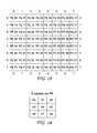
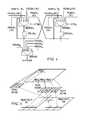
- FIG. 1 aan 8 ⁇ 8 PE array
- FIG. 1 bthe local memory of a PE
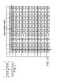
- FIGS. 2A-2Dthe structure of the main search area, extension areas and assignment of the related pixels to PEs;
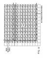
- FIG. 3exemplary neighbors for border and non-border PEs
- FIG. 4the circuitry of a particular communication register
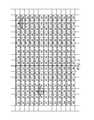
- FIG. 5the structure of PEs, their communication registers and input data field areas.
- each PEhas nine special registers X 0 , . . . , X 8 , each of which holding a reference pixel value.
- one register X 0holds the corresponding pixel of the corresponding block of the reference image
- three registers X 1 , X 3 , X 4hold corresponding pixels of neighboring blocks of the reference image that may be used for larger block sizes like 8 ⁇ 16, 16 ⁇ 8, 16 ⁇ 16
- five registers X 2 , X 5 , X 6 , X 7 , X 8are used to buffer pixels that are shifted in or out the 16 ⁇ 16 block X 0 -X 1 -X 3 -X 4 as described below.
- the neighboring reference blocksare e.g. those that are referred to as east X 1 , south X 3 and south-east X 4 .
- one register R 0holds a current pixel to be searched.
- each PEcan have further registers R 1 , R 2 , R 3 that hold e.g. three further pixels of the current block, if the current block is larger than 8 ⁇ 8. This allows block matching e.g. on 8 ⁇ 16, 16 ⁇ 8 or 16 ⁇ 16 blocks.
- FIGS. 2S-2Dshows an area of 24 ⁇ 24 pixels of a reference image, and where each pixel is locally stored in the PE grid.
- the main search area of the reference imageconsists in this example of four 8 ⁇ 8 blocks. E.g. the upper left corner of each block of the main search area is locally stored in PE 00 , in the registers X 0 , X 1 , X 3 and X 4 . In the same manner, the other reference pixels are distributed to the other PEs.
- a measure of similarity between a current block and a reference blockis determined, e.g. a sum-of-absolute-differences (SAD).
- SADsum-of-absolute-differences
- the PEcalculates the absolute difference
- the current pixels of an 8 ⁇ 16 blockare stored in the local registers R 0 and R 1 .
- the PEcalculates the absolute differences
- in one or two steps, depending on the PE hardware, and an accumulator calculates SAD⁇ (
- SAD⁇ (
- the pixels of the neighboring reference blockare locally available in the PE.
- the described grid of 8 ⁇ 8 PEs with each having four registers R 0 , . . . , R 3 for current valuesis optimized for applications that process blocks of 8 ⁇ 8 data, but can also handle blocks of 8 ⁇ 16, 16 ⁇ 8 or 16 ⁇ 16 data, as is the case for currently used ME algorithms.
- the SADis stored, the search area is moved and the SAD calculation is repeated.
- the block with the minimum SADis determined, and finally selected as reference block for determining a motion vector.
- the moving of the search areais generally done by shifting the search area and the reference area relative to each other, which is usually a complex process but much easier with the architecture of the invention.
- the larger search (or reference) areais shifted while the smaller current area is kept constant until all positions have been gone through.
- the current value in the R 0 -R 3 registersremains the same for each PE, while the values in the “special” registers (X 0 , . . . , X 8 ) are modified.
- these “special” registers(X 0 , . . . , X 8 ) are connected to the corresponding “special” registers of the neighboring PE by a switchable connection that implements a 2-dimensional shift register allowing north, east, south or west shifting. Since the PEs may communicate their values to the neighboring PEs via these registers (X 0 , . . . , X 8 ), they are called communication registers herein.
- the switchable connectiontypically uses multiplexers.
- the multiplexersare simple, e.g. 6:1, and are connected through short wires to a neighbor PE. Thus, high-frequency operation is possible.
- the pixels of each PEare simply shifted to its neighbor PE (in the currently used direction) by correspondingly controlling all multiplexers of the PE grid. Obviously it is very easy to change the search direction, namely by different multiplexer control.
- the neighbor mapping of border PEsis described below.
- a shift registerwhich provides an efficient way to exchange the search data between the PEs. It allows moving the search area pixel by pixel.
- a shift operation in “north” directionwill shift the pixels of a particular PE, e.g. PE 11 , to the corresponding registers of its northern neighbor PE 01 .
- the pixels that are shifted out of the search areaare input to the opposite side of the grid (though this is also known as “rotating”, the term “shift” is used herein).
- the pixels from PE 01are shifted to PE 71 . The same applies vice versa for “south” shifts, and further for “east” and “west” shifts.
- the communication registers of all PEsmake a 2-dimensional ring buffer.
- the search areais moved e.g. in a row or snake scan order over all possible positions within the 8 ⁇ 8 block.
- the contents of PE 00 X 0 , PE 10 X 0 , . . . , PE 70 X 0has been moved to PE 70 X 0 , PE 00 X 3 , . . . , PE 60 X 3 .
- Using snake scan ordercan mean that then an “east” shift follows, so that the contents of PE 70 X 0 , PE 00 X 3 , . . . , PE 60 X 3 is moved to PE 71 X 0 , PE 01 X 3 , . .
- Eis one “east” shift and PE calculation etc.
- the currently unused part of the reference imageis shifted into the extension registers X 2 , X 5 , X 6 , X 7 , X 8 and can be shifted back later.
- Other types of scan ordercan also be used, e.g. spiral scan starting from the middle block.
- the registers of the PEsare coequal, so that e.g. an 8 ⁇ 8 source block to be searched within the search area can be stored in the R 0 registers, but also e.g. in the R 3 registers instead, depending on the employed search strategy.
- the extension areacan also be on the upper or left side, as may be required e.g. for spiral scan, since also the communication registers X 0 -X 8 within a PE have coequal structures.
- this architectureis that the grid or array can be extended at the edges without limitation of the search area size, since only up to four of the communication registers are used as current search position. As indicated in FIGS. 2A-2D , these are the X 0 , X 1 , X 3 and X 4 registers of each PE. If processing e.g. a 16 ⁇ 16 block, each PE performs four calculations before the next shift, namely
- the communication registers of the respective extension areahold only data that were initially in the main search area. If snake scan order is used, these data will be shifted back.
- the passed time(4 ⁇ 8 cycles) may have been used to load new extension area data from the main image memory. This is advantageous because it does not require access to the main image memory at a particular time, but can be done at any time during these 32 cycles. This allows seamless operation of the ME also when the main image memory is slow or very busy.
- the new data from the main image memorymay be collected in an intermediate buffer, and copied into the communication registers of the extension area in a single step between the 8 th and the 9 th shift.
- the architecture according to the inventionis also advantageous for other types of processing, in particular image processing, such as e.g. 2-dimensional filtering.
- the number of PEs and/or the number of communication registers per PEmay vary according to the actual application.
- the PEshave local registers (communication registers) that can be connected dynamically into different types of shift registers that work as ring buffers, i.e. that don't lose data when shifting.
- this register structureit is possible to operate on a large input data field without the need to continuously access the source of this input data field. This is achieved by shifting the input data of a current operating step for re-usage in another or the same PE in the next operating step. Thus, in a way the input data are moved along the PEs rather than moving the PEs with their current intermediate result along the input data.
- FIG. 4shows exemplarily and only in principle the circuitry of a particular communication register X 1 of PE 43 , which is also highlighted in FIG. 3 .
- This register PE 43 X 1is via a multiplexer MX 43 X 1 connected to the local registers of PE 43 and to its neighbors, namely PE 53 X 1 in southern direction, PE 42 X 1 in western direction, PE 33 X 1 in northern direction and PE 44 X 1 in eastern direction.
- the valuesare shifted in the respective direction. Further, one multiplexer position is required for holding the current value, i.e. when no shift is performed.
- the control signal CTRLis in one embodiment the same for all communication registers and PEs.
- FIG. 4further shows that the actual processing unit PU 43 of the PE can be connected to any of its local communication registers via a further multiplexer MX 43 X.
- This connectionis switched depending on the current mode.
- the source blockis located in the upper left corner in 8 ⁇ 8 block mode then it is only X 0 , and in 16 ⁇ 16 block mode it is X 0 , X 1 , X 3 and X 4 .
- all the registers X 0 , . . . , X 8are equivalent the source block can be located anywhere.
- each of the nine communication registers of a PEhas only four connections outside the PE. All connections are local to the direct neighbor of the PE, and therefore short.
- the signal pathcomes from a register and has only a small multiplexer before it ends in the target register. Therefore the routing and timing closure for on-chip implementation is relatively easy.
- the PEsare connected to their neighbors and the borders are wrapped-around, no extra cycles are needed at the borders.
- the “east” neighbor of PE 07 X 2is PE 00 X 0
- its “northern” neighboris PE 77 X 8 .
- FIG. 5shows on top the PE array PE 00 , . . . , PE 77 from FIG. 1 , in a second layer the communication registers of the PEs PE 00 X 0 -X 8 , . . . , PE 77 X 0 -X 8 and in a third layer a part of the input data field, corresponding to the bottom right corner of FIG. 2 . Since the nine communication registers hold pixel data from different blocks, these pixels are not neighbors in the reference image but a kind of coarse representation of the current nine blocks. In principle, the architecture maps a multi-block data structure to a single block data structure, e.g. a 3 ⁇ 3 blocks reference area to a single block of PEs. Interconnections between communication registers are not shown in FIG. 5 .
- the processingcan be performed in the same cycle as the shifting. Therefore, if processing can be performed in one cycle as described above for the 8 ⁇ 8 block mode, the data can continuously be shifted and simultaneously processed by the PEs.
- the programming of the PE structure according to the inventionrequires simple but specialized commands, such as a command for selecting a shift mode or different commands for different shift modes, a command for loading data from an external (intermediate) memory into one of the extension areas etc.
- the architecture according to the inventionis also advantageous e.g. for 1-dimensional filtering. If input data are arranged in a row, e.g. a single line of pixels of image data, they may be organized in groups of n successive values. Instead of one register being associated with one PE, as usual, there are two or more registers connected to each PE. Each of these registers of a PE stores data from a different group of input data. The PE is connected via a multiplexer successively to each of its input registers and calculates a respective output value. Then the values are shifted to the neighboring PE. Different PEs may perform different operations, or the same type of operation on different data sets.
- a structure according to the inventionprovides e.g. a reduced data load time, short connections for the input data (which is advantageous for high-speed circuits) and flexibility since it can be switched or configured to handle different processing schemes.
- the inventionis advantageous for all kinds of processing structures that work on input data arrays, even two- or multi-dimensional input data fields, particularly if always the same type of calculation is performed.
Landscapes
- Engineering & Computer Science (AREA)
- Theoretical Computer Science (AREA)
- Computer Hardware Design (AREA)
- Physics & Mathematics (AREA)
- General Physics & Mathematics (AREA)
- Computing Systems (AREA)
- General Engineering & Computer Science (AREA)
- Image Processing (AREA)
- Compression, Expansion, Code Conversion, And Decoders (AREA)
Abstract
Description
Claims (14)
Applications Claiming Priority (3)
| Application Number | Priority Date | Filing Date | Title |
|---|---|---|---|
| EP06301200AEP1927949A1 (en) | 2006-12-01 | 2006-12-01 | Array of processing elements with local registers |
| EP06301200 | 2006-12-01 | ||
| EP06301200.9 | 2006-12-01 |
Publications (2)
| Publication Number | Publication Date |
|---|---|
| US20080133881A1 US20080133881A1 (en) | 2008-06-05 |
| US7941634B2true US7941634B2 (en) | 2011-05-10 |
Family
ID=37907631
Family Applications (1)
| Application Number | Title | Priority Date | Filing Date |
|---|---|---|---|
| US11/985,229Expired - Fee RelatedUS7941634B2 (en) | 2006-12-01 | 2007-11-14 | Array of processing elements with local registers |
Country Status (4)
| Country | Link |
|---|---|
| US (1) | US7941634B2 (en) |
| EP (1) | EP1927949A1 (en) |
| JP (1) | JP5131830B2 (en) |
| CN (1) | CN101202914B (en) |
Cited By (46)
| Publication number | Priority date | Publication date | Assignee | Title |
|---|---|---|---|---|
| US20050025248A1 (en)* | 2003-07-30 | 2005-02-03 | Johnson Timothy A. | Video compression system |
| US20070019743A1 (en)* | 2002-10-01 | 2007-01-25 | Avocent Corporation | Video compression encoder |
| US20070274382A1 (en)* | 2006-02-17 | 2007-11-29 | John Hickey | Video compression algorithm |
| US20080019441A1 (en)* | 2004-06-25 | 2008-01-24 | Avocent Corporation | Video compression noise immunity |
| US20090290647A1 (en)* | 2006-04-28 | 2009-11-26 | Avocent Corporation | DVC Delta commands |
| US20140149657A1 (en)* | 2012-01-10 | 2014-05-29 | Intel Corporation | Intelligent parametric scratchap memory architecture |
| US9749548B2 (en) | 2015-01-22 | 2017-08-29 | Google Inc. | Virtual linebuffers for image signal processors |
| US9756268B2 (en) | 2015-04-23 | 2017-09-05 | Google Inc. | Line buffer unit for image processor |
| US9769356B2 (en) | 2015-04-23 | 2017-09-19 | Google Inc. | Two dimensional shift array for image processor |
| US9772852B2 (en) | 2015-04-23 | 2017-09-26 | Google Inc. | Energy efficient processor core architecture for image processor |
| US9785423B2 (en) | 2015-04-23 | 2017-10-10 | Google Inc. | Compiler for translating between a virtual image processor instruction set architecture (ISA) and target hardware having a two-dimensional shift array structure |
| US9830150B2 (en) | 2015-12-04 | 2017-11-28 | Google Llc | Multi-functional execution lane for image processor |
| US9965824B2 (en) | 2015-04-23 | 2018-05-08 | Google Llc | Architecture for high performance, power efficient, programmable image processing |
| US9978116B2 (en) | 2016-07-01 | 2018-05-22 | Google Llc | Core processes for block operations on an image processor having a two-dimensional execution lane array and a two-dimensional shift register |
| US9986187B2 (en) | 2016-07-01 | 2018-05-29 | Google Llc | Block operations for an image processor having a two-dimensional execution lane array and a two-dimensional shift register |
| US10095479B2 (en) | 2015-04-23 | 2018-10-09 | Google Llc | Virtual image processor instruction set architecture (ISA) and memory model and exemplary target hardware having a two-dimensional shift array structure |
| US10205896B2 (en) | 2015-07-24 | 2019-02-12 | Google Llc | Automatic lens flare detection and correction for light-field images |
| US10204396B2 (en) | 2016-02-26 | 2019-02-12 | Google Llc | Compiler managed memory for image processor |
| US10275898B1 (en) | 2015-04-15 | 2019-04-30 | Google Llc | Wedge-based light-field video capture |
| US10275892B2 (en) | 2016-06-09 | 2019-04-30 | Google Llc | Multi-view scene segmentation and propagation |
| US10284744B2 (en) | 2015-04-23 | 2019-05-07 | Google Llc | Sheet generator for image processor |
| US10298834B2 (en) | 2006-12-01 | 2019-05-21 | Google Llc | Video refocusing |
| US10313641B2 (en)* | 2015-12-04 | 2019-06-04 | Google Llc | Shift register with reduced wiring complexity |
| US10334151B2 (en) | 2013-04-22 | 2019-06-25 | Google Llc | Phase detection autofocus using subaperture images |
| US10341632B2 (en) | 2015-04-15 | 2019-07-02 | Google Llc. | Spatial random access enabled video system with a three-dimensional viewing volume |
| US10354399B2 (en) | 2017-05-25 | 2019-07-16 | Google Llc | Multi-view back-projection to a light-field |
| US10380969B2 (en) | 2016-02-28 | 2019-08-13 | Google Llc | Macro I/O unit for image processor |
| US10387989B2 (en)* | 2016-02-26 | 2019-08-20 | Google Llc | Compiler techniques for mapping program code to a high performance, power efficient, programmable image processing hardware platform |
| US10412373B2 (en) | 2015-04-15 | 2019-09-10 | Google Llc | Image capture for virtual reality displays |
| US10419737B2 (en) | 2015-04-15 | 2019-09-17 | Google Llc | Data structures and delivery methods for expediting virtual reality playback |
| US10440407B2 (en) | 2017-05-09 | 2019-10-08 | Google Llc | Adaptive control for immersive experience delivery |
| US10444931B2 (en) | 2017-05-09 | 2019-10-15 | Google Llc | Vantage generation and interactive playback |
| US10469873B2 (en) | 2015-04-15 | 2019-11-05 | Google Llc | Encoding and decoding virtual reality video |
| US10474227B2 (en) | 2017-05-09 | 2019-11-12 | Google Llc | Generation of virtual reality with 6 degrees of freedom from limited viewer data |
| US10540818B2 (en) | 2015-04-15 | 2020-01-21 | Google Llc | Stereo image generation and interactive playback |
| US10545215B2 (en) | 2017-09-13 | 2020-01-28 | Google Llc | 4D camera tracking and optical stabilization |
| US10546424B2 (en) | 2015-04-15 | 2020-01-28 | Google Llc | Layered content delivery for virtual and augmented reality experiences |
| US10546211B2 (en) | 2016-07-01 | 2020-01-28 | Google Llc | Convolutional neural network on programmable two dimensional image processor |
| US10552947B2 (en) | 2012-06-26 | 2020-02-04 | Google Llc | Depth-based image blurring |
| US10567464B2 (en) | 2015-04-15 | 2020-02-18 | Google Llc | Video compression with adaptive view-dependent lighting removal |
| US10565734B2 (en) | 2015-04-15 | 2020-02-18 | Google Llc | Video capture, processing, calibration, computational fiber artifact removal, and light-field pipeline |
| US10594945B2 (en) | 2017-04-03 | 2020-03-17 | Google Llc | Generating dolly zoom effect using light field image data |
| US10679361B2 (en) | 2016-12-05 | 2020-06-09 | Google Llc | Multi-view rotoscope contour propagation |
| US10915773B2 (en) | 2016-07-01 | 2021-02-09 | Google Llc | Statistics operations on two dimensional image processor |
| US10965862B2 (en) | 2018-01-18 | 2021-03-30 | Google Llc | Multi-camera navigation interface |
| US11328446B2 (en) | 2015-04-15 | 2022-05-10 | Google Llc | Combining light-field data with active depth data for depth map generation |
Families Citing this family (5)
| Publication number | Priority date | Publication date | Assignee | Title |
|---|---|---|---|---|
| GB201007406D0 (en)* | 2010-05-04 | 2010-06-16 | Aspex Semiconductor Ltd | Block motion estimation |
| US11294815B2 (en)* | 2015-06-10 | 2022-04-05 | Mobileye Vision Technologies Ltd. | Multiple multithreaded processors with shared data cache |
| US10719323B2 (en) | 2018-09-27 | 2020-07-21 | Intel Corporation | Systems and methods for performing matrix compress and decompress instructions |
| US20200210517A1 (en) | 2018-12-27 | 2020-07-02 | Intel Corporation | Systems and methods to accelerate multiplication of sparse matrices |
| CN116366851A (en)* | 2022-12-16 | 2023-06-30 | 联发科技股份有限公司 | Video data encoding method and device |
Citations (19)
| Publication number | Priority date | Publication date | Assignee | Title |
|---|---|---|---|---|
| US3544973A (en)* | 1968-03-13 | 1970-12-01 | Westinghouse Electric Corp | Variable structure computer |
| US4380046A (en)* | 1979-05-21 | 1983-04-12 | Nasa | Massively parallel processor computer |
| US4811413A (en)* | 1987-10-22 | 1989-03-07 | International Business Machines Corp. | System of reconfigurable pipelines of generalized neighborhood function morphic image processors |
| US5179714A (en)* | 1988-10-07 | 1993-01-12 | Martin Marietta Corporation | Parallel bit serial data processor |
| WO1994009595A1 (en) | 1991-09-20 | 1994-04-28 | Shaw Venson M | Method and apparatus including system architecture for multimedia communications |
| US5400087A (en) | 1992-07-06 | 1995-03-21 | Mitsubishi Denki Kabushiki Kaisha | Motion vector detecting device for compensating for movements in a motion picture |
| US5428804A (en)* | 1992-12-18 | 1995-06-27 | Xerox Corporation | Edge crossing circuitry for SIMD architecture |
| US5838827A (en)* | 1994-11-10 | 1998-11-17 | Graphics Communication Laboratories | Apparatus and method for searching motion vector |
| US6118901A (en) | 1997-10-31 | 2000-09-12 | National Science Council | Array architecture with data-rings for 3-step hierarchical search block matching algorithm |
| US6356945B1 (en)* | 1991-09-20 | 2002-03-12 | Venson M. Shaw | Method and apparatus including system architecture for multimedia communications |
| US20020113196A1 (en)* | 2001-02-20 | 2002-08-22 | Syscan Technology (Shenzhen) Co., Limited | Method and apparatus for scanning colors using multiple arrays of photodetectors |
| US20020130944A1 (en)* | 2001-03-14 | 2002-09-19 | Hidetoshi Ema | Light-emission modulation having effective scheme of creating gray scale on image |
| US20020144082A1 (en) | 1998-06-05 | 2002-10-03 | Bops, Inc. | Methods and apparatus for ManArray PE-PE switch control |
| US20030016748A1 (en) | 2001-07-20 | 2003-01-23 | Divio, Inc. | Memory control apparatus and efficient search pattern for block-matching motion estimation |
| US20030118108A1 (en)* | 2001-12-20 | 2003-06-26 | Lg Electronics Inc. | Apparatus and method for encoding and decoding moving picture using wavelet transformation and motion estimation |
| US6643763B1 (en) | 2000-02-28 | 2003-11-04 | International Business Machines Corporation | Register pipe for multi-processing engine environment |
| US20070136560A1 (en)* | 2000-08-22 | 2007-06-14 | Graham Kirsch | Method and apparatus for a shift register based interconnection for a massively parallel processor array |
| US7483420B1 (en)* | 2004-03-08 | 2009-01-27 | Altera Corporation | DSP circuitry for supporting multi-channel applications by selectively shifting data through registers |
| US7539845B1 (en)* | 2006-04-14 | 2009-05-26 | Tilera Corporation | Coupling integrated circuits in a parallel processing environment |
Family Cites Families (7)
| Publication number | Priority date | Publication date | Assignee | Title |
|---|---|---|---|---|
| JP2717850B2 (en)* | 1989-05-30 | 1998-02-25 | 富士通株式会社 | Parallel computer with high-speed communication mechanism |
| JP3084170B2 (en)* | 1992-08-13 | 2000-09-04 | 三菱電機株式会社 | Motion vector detection device |
| CN1075646C (en)* | 1996-01-19 | 2001-11-28 | 张胤微 | High-speed multiplication device |
| DE10005911A1 (en)* | 2000-02-10 | 2001-08-16 | Philips Corp Intellectual Pty | Control unit for a terminal of a digital cordless telecommunication system and method for such a control unit |
| US6928593B1 (en)* | 2000-09-18 | 2005-08-09 | Intel Corporation | Memory module and memory component built-in self test |
| FR2865290A1 (en)* | 2004-01-21 | 2005-07-22 | Thomson Licensing Sa | METHOD FOR MANAGING DATA IN A MATRIX PROCESSOR AND MATRIX PROCESSOR EMPLOYING THE METHOD |
| CN100372317C (en)* | 2005-05-13 | 2008-02-27 | 清华大学 | 10G network performance tester traffic receiving, grabbing and statistical circuit components |
- 2006
- 2006-12-01EPEP06301200Apatent/EP1927949A1/ennot_activeWithdrawn
- 2007
- 2007-11-14USUS11/985,229patent/US7941634B2/ennot_activeExpired - Fee Related
- 2007-11-29CNCN2007101966391Apatent/CN101202914B/ennot_activeExpired - Fee Related
- 2007-11-29JPJP2007308198Apatent/JP5131830B2/ennot_activeExpired - Fee Related
Patent Citations (19)
| Publication number | Priority date | Publication date | Assignee | Title |
|---|---|---|---|---|
| US3544973A (en)* | 1968-03-13 | 1970-12-01 | Westinghouse Electric Corp | Variable structure computer |
| US4380046A (en)* | 1979-05-21 | 1983-04-12 | Nasa | Massively parallel processor computer |
| US4811413A (en)* | 1987-10-22 | 1989-03-07 | International Business Machines Corp. | System of reconfigurable pipelines of generalized neighborhood function morphic image processors |
| US5179714A (en)* | 1988-10-07 | 1993-01-12 | Martin Marietta Corporation | Parallel bit serial data processor |
| US6356945B1 (en)* | 1991-09-20 | 2002-03-12 | Venson M. Shaw | Method and apparatus including system architecture for multimedia communications |
| WO1994009595A1 (en) | 1991-09-20 | 1994-04-28 | Shaw Venson M | Method and apparatus including system architecture for multimedia communications |
| US5400087A (en) | 1992-07-06 | 1995-03-21 | Mitsubishi Denki Kabushiki Kaisha | Motion vector detecting device for compensating for movements in a motion picture |
| US5428804A (en)* | 1992-12-18 | 1995-06-27 | Xerox Corporation | Edge crossing circuitry for SIMD architecture |
| US5838827A (en)* | 1994-11-10 | 1998-11-17 | Graphics Communication Laboratories | Apparatus and method for searching motion vector |
| US6118901A (en) | 1997-10-31 | 2000-09-12 | National Science Council | Array architecture with data-rings for 3-step hierarchical search block matching algorithm |
| US20020144082A1 (en) | 1998-06-05 | 2002-10-03 | Bops, Inc. | Methods and apparatus for ManArray PE-PE switch control |
| US6643763B1 (en) | 2000-02-28 | 2003-11-04 | International Business Machines Corporation | Register pipe for multi-processing engine environment |
| US20070136560A1 (en)* | 2000-08-22 | 2007-06-14 | Graham Kirsch | Method and apparatus for a shift register based interconnection for a massively parallel processor array |
| US20020113196A1 (en)* | 2001-02-20 | 2002-08-22 | Syscan Technology (Shenzhen) Co., Limited | Method and apparatus for scanning colors using multiple arrays of photodetectors |
| US20020130944A1 (en)* | 2001-03-14 | 2002-09-19 | Hidetoshi Ema | Light-emission modulation having effective scheme of creating gray scale on image |
| US20030016748A1 (en) | 2001-07-20 | 2003-01-23 | Divio, Inc. | Memory control apparatus and efficient search pattern for block-matching motion estimation |
| US20030118108A1 (en)* | 2001-12-20 | 2003-06-26 | Lg Electronics Inc. | Apparatus and method for encoding and decoding moving picture using wavelet transformation and motion estimation |
| US7483420B1 (en)* | 2004-03-08 | 2009-01-27 | Altera Corporation | DSP circuitry for supporting multi-channel applications by selectively shifting data through registers |
| US7539845B1 (en)* | 2006-04-14 | 2009-05-26 | Tilera Corporation | Coupling integrated circuits in a parallel processing environment |
Non-Patent Citations (4)
| Title |
|---|
| Chang, Y-C, et al., "Advances in Hardware Architectures for Image and Video Coding-A Survey"Proceedings of the IEEE, vol. 93, No. 1, Jan. 2005; pp. 184-197. |
| European Search Report for EP 07 12 0961 dated Mar. 14, 2008. |
| Hang et al., "Motion Estimation for Video Coding Standards", Journal of VLSI Signal Processing Systems for Signa, Image, and Video Technology, Springer, NY, vol. 17 No. 2/3, Nov. 1997, pp. 113-136. |
| Search Report dated Apr. 16, 2007. |
Cited By (88)
| Publication number | Priority date | Publication date | Assignee | Title |
|---|---|---|---|---|
| US20070019743A1 (en)* | 2002-10-01 | 2007-01-25 | Avocent Corporation | Video compression encoder |
| US8385429B2 (en) | 2002-10-01 | 2013-02-26 | Avocent Corporation | Video compression encoder |
| US9743095B2 (en) | 2002-10-01 | 2017-08-22 | Avocent Corporation | Video compression encoder |
| US20050025248A1 (en)* | 2003-07-30 | 2005-02-03 | Johnson Timothy A. | Video compression system |
| US9560371B2 (en) | 2003-07-30 | 2017-01-31 | Avocent Corporation | Video compression system |
| US8805096B2 (en) | 2004-06-25 | 2014-08-12 | Avocent Corporation | Video compression noise immunity |
| US20080019441A1 (en)* | 2004-06-25 | 2008-01-24 | Avocent Corporation | Video compression noise immunity |
| US20070274382A1 (en)* | 2006-02-17 | 2007-11-29 | John Hickey | Video compression algorithm |
| US8718147B2 (en)* | 2006-02-17 | 2014-05-06 | Avocent Huntsville Corporation | Video compression algorithm |
| US20090290647A1 (en)* | 2006-04-28 | 2009-11-26 | Avocent Corporation | DVC Delta commands |
| US8660194B2 (en) | 2006-04-28 | 2014-02-25 | Avocent Corporation | DVC delta commands |
| US10298834B2 (en) | 2006-12-01 | 2019-05-21 | Google Llc | Video refocusing |
| US9329834B2 (en)* | 2012-01-10 | 2016-05-03 | Intel Corporation | Intelligent parametric scratchap memory architecture |
| US20140149657A1 (en)* | 2012-01-10 | 2014-05-29 | Intel Corporation | Intelligent parametric scratchap memory architecture |
| US10001971B2 (en) | 2012-01-10 | 2018-06-19 | Intel Corporation | Electronic apparatus having parallel memory banks |
| US10552947B2 (en) | 2012-06-26 | 2020-02-04 | Google Llc | Depth-based image blurring |
| US10334151B2 (en) | 2013-04-22 | 2019-06-25 | Google Llc | Phase detection autofocus using subaperture images |
| US10516833B2 (en) | 2015-01-22 | 2019-12-24 | Google Llc | Virtual linebuffers for image signal processors |
| US10277833B2 (en) | 2015-01-22 | 2019-04-30 | Google Llc | Virtual linebuffers for image signal processors |
| US9749548B2 (en) | 2015-01-22 | 2017-08-29 | Google Inc. | Virtual linebuffers for image signal processors |
| US10791284B2 (en) | 2015-01-22 | 2020-09-29 | Google Llc | Virtual linebuffers for image signal processors |
| US10469873B2 (en) | 2015-04-15 | 2019-11-05 | Google Llc | Encoding and decoding virtual reality video |
| US10565734B2 (en) | 2015-04-15 | 2020-02-18 | Google Llc | Video capture, processing, calibration, computational fiber artifact removal, and light-field pipeline |
| US10540818B2 (en) | 2015-04-15 | 2020-01-21 | Google Llc | Stereo image generation and interactive playback |
| US10567464B2 (en) | 2015-04-15 | 2020-02-18 | Google Llc | Video compression with adaptive view-dependent lighting removal |
| US10419737B2 (en) | 2015-04-15 | 2019-09-17 | Google Llc | Data structures and delivery methods for expediting virtual reality playback |
| US10412373B2 (en) | 2015-04-15 | 2019-09-10 | Google Llc | Image capture for virtual reality displays |
| US10341632B2 (en) | 2015-04-15 | 2019-07-02 | Google Llc. | Spatial random access enabled video system with a three-dimensional viewing volume |
| US11328446B2 (en) | 2015-04-15 | 2022-05-10 | Google Llc | Combining light-field data with active depth data for depth map generation |
| US10546424B2 (en) | 2015-04-15 | 2020-01-28 | Google Llc | Layered content delivery for virtual and augmented reality experiences |
| US10275898B1 (en) | 2015-04-15 | 2019-04-30 | Google Llc | Wedge-based light-field video capture |
| US10095479B2 (en) | 2015-04-23 | 2018-10-09 | Google Llc | Virtual image processor instruction set architecture (ISA) and memory model and exemplary target hardware having a two-dimensional shift array structure |
| US9769356B2 (en) | 2015-04-23 | 2017-09-19 | Google Inc. | Two dimensional shift array for image processor |
| US10284744B2 (en) | 2015-04-23 | 2019-05-07 | Google Llc | Sheet generator for image processor |
| US10291813B2 (en) | 2015-04-23 | 2019-05-14 | Google Llc | Sheet generator for image processor |
| US10275253B2 (en) | 2015-04-23 | 2019-04-30 | Google Llc | Energy efficient processor core architecture for image processor |
| US9772852B2 (en) | 2015-04-23 | 2017-09-26 | Google Inc. | Energy efficient processor core architecture for image processor |
| US9785423B2 (en) | 2015-04-23 | 2017-10-10 | Google Inc. | Compiler for translating between a virtual image processor instruction set architecture (ISA) and target hardware having a two-dimensional shift array structure |
| US9756268B2 (en) | 2015-04-23 | 2017-09-05 | Google Inc. | Line buffer unit for image processor |
| US10216487B2 (en)* | 2015-04-23 | 2019-02-26 | Google Llc | Virtual image processor instruction set architecture (ISA) and memory model and exemplary target hardware having a two-dimensional shift array structure |
| US10560598B2 (en) | 2015-04-23 | 2020-02-11 | Google Llc | Sheet generator for image processor |
| US11190718B2 (en) | 2015-04-23 | 2021-11-30 | Google Llc | Line buffer unit for image processor |
| US11182138B2 (en) | 2015-04-23 | 2021-11-23 | Google Llc | Compiler for translating between a virtual image processor instruction set architecture (ISA) and target hardware having a two-dimensional shift array structure |
| US10638073B2 (en) | 2015-04-23 | 2020-04-28 | Google Llc | Line buffer unit for image processor |
| US9965824B2 (en) | 2015-04-23 | 2018-05-08 | Google Llc | Architecture for high performance, power efficient, programmable image processing |
| US10397450B2 (en) | 2015-04-23 | 2019-08-27 | Google Llc | Two dimensional shift array for image processor |
| US10719905B2 (en)* | 2015-04-23 | 2020-07-21 | Google Llc | Architecture for high performance, power efficient, programmable image processing |
| US10754654B2 (en) | 2015-04-23 | 2020-08-25 | Google Llc | Energy efficient processor core architecture for image processor |
| US10417732B2 (en) | 2015-04-23 | 2019-09-17 | Google Llc | Architecture for high performance, power efficient, programmable image processing |
| US11153464B2 (en) | 2015-04-23 | 2021-10-19 | Google Llc | Two dimensional shift array for image processor |
| US11140293B2 (en) | 2015-04-23 | 2021-10-05 | Google Llc | Sheet generator for image processor |
| US10095492B2 (en) | 2015-04-23 | 2018-10-09 | Google Llc | Compiler for translating between a virtual image processor instruction set architecture (ISA) and target hardware having a two-dimensional shift array structure |
| US11138013B2 (en) | 2015-04-23 | 2021-10-05 | Google Llc | Energy efficient processor core architecture for image processor |
| US10599407B2 (en) | 2015-04-23 | 2020-03-24 | Google Llc | Compiler for translating between a virtual image processor instruction set architecture (ISA) and target hardware having a two-dimensional shift array structure |
| US20190378239A1 (en)* | 2015-04-23 | 2019-12-12 | Google Llc | Architecture for high performance, power efficient, programmable image processing |
| US10205896B2 (en) | 2015-07-24 | 2019-02-12 | Google Llc | Automatic lens flare detection and correction for light-field images |
| US10998070B2 (en) | 2015-12-04 | 2021-05-04 | Google Llc | Shift register with reduced wiring complexity |
| US10477164B2 (en) | 2015-12-04 | 2019-11-12 | Google Llc | Shift register with reduced wiring complexity |
| US10185560B2 (en) | 2015-12-04 | 2019-01-22 | Google Llc | Multi-functional execution lane for image processor |
| US9830150B2 (en) | 2015-12-04 | 2017-11-28 | Google Llc | Multi-functional execution lane for image processor |
| US10313641B2 (en)* | 2015-12-04 | 2019-06-04 | Google Llc | Shift register with reduced wiring complexity |
| US20200020069A1 (en)* | 2016-02-26 | 2020-01-16 | Google Llc | Compiler techniques for mapping program code to a high performance, power efficient, programmable image processing hardware platform |
| US10685422B2 (en) | 2016-02-26 | 2020-06-16 | Google Llc | Compiler managed memory for image processor |
| US10387988B2 (en)* | 2016-02-26 | 2019-08-20 | Google Llc | Compiler techniques for mapping program code to a high performance, power efficient, programmable image processing hardware platform |
| US10387989B2 (en)* | 2016-02-26 | 2019-08-20 | Google Llc | Compiler techniques for mapping program code to a high performance, power efficient, programmable image processing hardware platform |
| US10204396B2 (en) | 2016-02-26 | 2019-02-12 | Google Llc | Compiler managed memory for image processor |
| US10304156B2 (en) | 2016-02-26 | 2019-05-28 | Google Llc | Compiler managed memory for image processor |
| US10733956B2 (en) | 2016-02-28 | 2020-08-04 | Google Llc | Macro I/O unit for image processor |
| US10504480B2 (en) | 2016-02-28 | 2019-12-10 | Google Llc | Macro I/O unit for image processor |
| US10380969B2 (en) | 2016-02-28 | 2019-08-13 | Google Llc | Macro I/O unit for image processor |
| US10275892B2 (en) | 2016-06-09 | 2019-04-30 | Google Llc | Multi-view scene segmentation and propagation |
| US10546211B2 (en) | 2016-07-01 | 2020-01-28 | Google Llc | Convolutional neural network on programmable two dimensional image processor |
| US11196953B2 (en) | 2016-07-01 | 2021-12-07 | Google Llc | Block operations for an image processor having a two-dimensional execution lane array and a two-dimensional shift register |
| US10531030B2 (en) | 2016-07-01 | 2020-01-07 | Google Llc | Block operations for an image processor having a two-dimensional execution lane array and a two-dimensional shift register |
| US10789505B2 (en) | 2016-07-01 | 2020-09-29 | Google Llc | Convolutional neural network on programmable two dimensional image processor |
| US9986187B2 (en) | 2016-07-01 | 2018-05-29 | Google Llc | Block operations for an image processor having a two-dimensional execution lane array and a two-dimensional shift register |
| US10915773B2 (en) | 2016-07-01 | 2021-02-09 | Google Llc | Statistics operations on two dimensional image processor |
| US12020027B2 (en) | 2016-07-01 | 2024-06-25 | Google Llc | Convolutional neural network on programmable two dimensional image processor |
| US9978116B2 (en) | 2016-07-01 | 2018-05-22 | Google Llc | Core processes for block operations on an image processor having a two-dimensional execution lane array and a two-dimensional shift register |
| US10334194B2 (en) | 2016-07-01 | 2019-06-25 | Google Llc | Block operations for an image processor having a two-dimensional execution lane array and a two-dimensional shift register |
| US10679361B2 (en) | 2016-12-05 | 2020-06-09 | Google Llc | Multi-view rotoscope contour propagation |
| US10594945B2 (en) | 2017-04-03 | 2020-03-17 | Google Llc | Generating dolly zoom effect using light field image data |
| US10474227B2 (en) | 2017-05-09 | 2019-11-12 | Google Llc | Generation of virtual reality with 6 degrees of freedom from limited viewer data |
| US10440407B2 (en) | 2017-05-09 | 2019-10-08 | Google Llc | Adaptive control for immersive experience delivery |
| US10444931B2 (en) | 2017-05-09 | 2019-10-15 | Google Llc | Vantage generation and interactive playback |
| US10354399B2 (en) | 2017-05-25 | 2019-07-16 | Google Llc | Multi-view back-projection to a light-field |
| US10545215B2 (en) | 2017-09-13 | 2020-01-28 | Google Llc | 4D camera tracking and optical stabilization |
| US10965862B2 (en) | 2018-01-18 | 2021-03-30 | Google Llc | Multi-camera navigation interface |
Also Published As
| Publication number | Publication date |
|---|---|
| JP5131830B2 (en) | 2013-01-30 |
| US20080133881A1 (en) | 2008-06-05 |
| JP2008165756A (en) | 2008-07-17 |
| EP1927949A1 (en) | 2008-06-04 |
| CN101202914B (en) | 2012-01-11 |
| CN101202914A (en) | 2008-06-18 |
Similar Documents
| Publication | Publication Date | Title |
|---|---|---|
| US7941634B2 (en) | Array of processing elements with local registers | |
| EP1120747A2 (en) | Motion estimator | |
| CN101156450A (en) | Region- based 3drs motion estimation using dynamic asoect ratio of region | |
| KR100280854B1 (en) | Data processing device and data processing method | |
| JP2001250113A (en) | Signal processing device and image signal processing system | |
| CN101156451A (en) | Video processing with region-based multiple-pass motion estimation and update of temporal motion vector candidates | |
| US4747154A (en) | Image data expanding and/or contracting method and apparatus | |
| JPH0789372B2 (en) | Image processing device | |
| JP2015529363A (en) | Processor, system and method for efficient and fast processing of interrelated two-dimensional data sets | |
| JP2010505158A (en) | Data processing with multiple memory banks | |
| KR20040050829A (en) | Semiconductor device, image data processing apparatus and method | |
| KR20080044102A (en) | Single instruction multiple data processor and memory array structure for it | |
| US6850569B2 (en) | Effective motion estimation for hierarchical search | |
| Nicol | A systolic approach for real time connected component labeling | |
| JP2002304624A (en) | Filter processing device and imaging device | |
| JP2005514677A (en) | Improvements in memory address technology | |
| KR20100049620A (en) | Device for motion search in dynamic image encoding | |
| EP1927950A1 (en) | Array of processing elements with local registers | |
| US7596679B2 (en) | Interconnections in SIMD processor architectures | |
| US6425026B1 (en) | Distribution, processing, and reconstruction of variable-sized images using multiple processor arrays | |
| EP0963108A2 (en) | Motion vector detection circuit enabling high-speed search of motion vector | |
| JP2007206887A (en) | LSI chip and arithmetic processing system | |
| WO2006120620A2 (en) | Image processing circuit with block accessible buffer memory | |
| EP0711039B1 (en) | General purpose charge mode analog operation circuit | |
| US7756207B2 (en) | Method for pre-processing block based digital data |
Legal Events
| Date | Code | Title | Description |
|---|---|---|---|
| AS | Assignment | Owner name:THOMSON LICENSING, FRANCE Free format text:ASSIGNMENT OF ASSIGNORS INTEREST;ASSIGNORS:BORSUM, MALTE;GAEDKE, KLAUS;GEORGI, MARCO;REEL/FRAME:020163/0720;SIGNING DATES FROM 20070816 TO 20070829 Owner name:THOMSON LICENSING, FRANCE Free format text:ASSIGNMENT OF ASSIGNORS INTEREST;ASSIGNORS:BORSUM, MALTE;GAEDKE, KLAUS;GEORGI, MARCO;SIGNING DATES FROM 20070816 TO 20070829;REEL/FRAME:020163/0720 | |
| STCF | Information on status: patent grant | Free format text:PATENTED CASE | |
| FPAY | Fee payment | Year of fee payment:4 | |
| AS | Assignment | Owner name:INTERDIGITAL VC HOLDINGS, INC., DELAWARE Free format text:ASSIGNMENT OF ASSIGNORS INTEREST;ASSIGNOR:THOMSON LICENSING;REEL/FRAME:047289/0698 Effective date:20180730 | |
| MAFP | Maintenance fee payment | Free format text:PAYMENT OF MAINTENANCE FEE, 8TH YEAR, LARGE ENTITY (ORIGINAL EVENT CODE: M1552); ENTITY STATUS OF PATENT OWNER: LARGE ENTITY Year of fee payment:8 | |
| FEPP | Fee payment procedure | Free format text:MAINTENANCE FEE REMINDER MAILED (ORIGINAL EVENT CODE: REM.); ENTITY STATUS OF PATENT OWNER: LARGE ENTITY | |
| LAPS | Lapse for failure to pay maintenance fees | Free format text:PATENT EXPIRED FOR FAILURE TO PAY MAINTENANCE FEES (ORIGINAL EVENT CODE: EXP.); ENTITY STATUS OF PATENT OWNER: LARGE ENTITY | |
| STCH | Information on status: patent discontinuation | Free format text:PATENT EXPIRED DUE TO NONPAYMENT OF MAINTENANCE FEES UNDER 37 CFR 1.362 | |
| FP | Lapsed due to failure to pay maintenance fee | Effective date:20230510 |