US7939842B2 - Light emitting device packages, light emitting diode (LED) packages and related methods - Google Patents
Light emitting device packages, light emitting diode (LED) packages and related methodsDownload PDFInfo
- Publication number
- US7939842B2 US7939842B2US11/895,795US89579507AUS7939842B2US 7939842 B2US7939842 B2US 7939842B2US 89579507 AUS89579507 AUS 89579507AUS 7939842 B2US7939842 B2US 7939842B2
- Authority
- US
- United States
- Prior art keywords
- encapsulant
- lens
- light emitting
- depression
- emitting device
- Prior art date
- Legal status (The legal status is an assumption and is not a legal conclusion. Google has not performed a legal analysis and makes no representation as to the accuracy of the status listed.)
- Active, expires
Links
Images


Classifications
- H—ELECTRICITY
- H10—SEMICONDUCTOR DEVICES; ELECTRIC SOLID-STATE DEVICES NOT OTHERWISE PROVIDED FOR
- H10H—INORGANIC LIGHT-EMITTING SEMICONDUCTOR DEVICES HAVING POTENTIAL BARRIERS
- H10H20/00—Individual inorganic light-emitting semiconductor devices having potential barriers, e.g. light-emitting diodes [LED]
- H10H20/80—Constructional details
- H10H20/85—Packages
- H10H20/852—Encapsulations
- H—ELECTRICITY
- H01—ELECTRIC ELEMENTS
- H01L—SEMICONDUCTOR DEVICES NOT COVERED BY CLASS H10
- H01L2224/00—Indexing scheme for arrangements for connecting or disconnecting semiconductor or solid-state bodies and methods related thereto as covered by H01L24/00
- H01L2224/01—Means for bonding being attached to, or being formed on, the surface to be connected, e.g. chip-to-package, die-attach, "first-level" interconnects; Manufacturing methods related thereto
- H01L2224/42—Wire connectors; Manufacturing methods related thereto
- H01L2224/47—Structure, shape, material or disposition of the wire connectors after the connecting process
- H01L2224/48—Structure, shape, material or disposition of the wire connectors after the connecting process of an individual wire connector
- H01L2224/4805—Shape
- H01L2224/4809—Loop shape
- H01L2224/48091—Arched
- H—ELECTRICITY
- H01—ELECTRIC ELEMENTS
- H01L—SEMICONDUCTOR DEVICES NOT COVERED BY CLASS H10
- H01L2224/00—Indexing scheme for arrangements for connecting or disconnecting semiconductor or solid-state bodies and methods related thereto as covered by H01L24/00
- H01L2224/01—Means for bonding being attached to, or being formed on, the surface to be connected, e.g. chip-to-package, die-attach, "first-level" interconnects; Manufacturing methods related thereto
- H01L2224/42—Wire connectors; Manufacturing methods related thereto
- H01L2224/47—Structure, shape, material or disposition of the wire connectors after the connecting process
- H01L2224/48—Structure, shape, material or disposition of the wire connectors after the connecting process of an individual wire connector
- H01L2224/484—Connecting portions
- H01L2224/4847—Connecting portions the connecting portion on the bonding area of the semiconductor or solid-state body being a wedge bond
- H01L2224/48471—Connecting portions the connecting portion on the bonding area of the semiconductor or solid-state body being a wedge bond the other connecting portion not on the bonding area being a ball bond, i.e. wedge-to-ball, reverse stitch
- H—ELECTRICITY
- H10—SEMICONDUCTOR DEVICES; ELECTRIC SOLID-STATE DEVICES NOT OTHERWISE PROVIDED FOR
- H10H—INORGANIC LIGHT-EMITTING SEMICONDUCTOR DEVICES HAVING POTENTIAL BARRIERS
- H10H20/00—Individual inorganic light-emitting semiconductor devices having potential barriers, e.g. light-emitting diodes [LED]
- H10H20/80—Constructional details
- H10H20/85—Packages
- H10H20/852—Encapsulations
- H10H20/853—Encapsulations characterised by their shape
- H—ELECTRICITY
- H10—SEMICONDUCTOR DEVICES; ELECTRIC SOLID-STATE DEVICES NOT OTHERWISE PROVIDED FOR
- H10H—INORGANIC LIGHT-EMITTING SEMICONDUCTOR DEVICES HAVING POTENTIAL BARRIERS
- H10H20/00—Individual inorganic light-emitting semiconductor devices having potential barriers, e.g. light-emitting diodes [LED]
- H10H20/80—Constructional details
- H10H20/85—Packages
- H10H20/855—Optical field-shaping means, e.g. lenses
Definitions
- the subject matter described hereinrelates to semiconductor device packages. More particularly, the subject matter described herein relates to light emitting device packages, light emitting diode packages and related methods.
- LEDsSemiconductor light emitting devices, such as a light emitting diode (LED), may be provided in a package for protection, color selection, focusing, and the like for light emitted by the device.
- An LED packagegenerally includes a substrate member on which an LED is mounted.
- the LEDmay include a mounting pad attached to the substrate member with electrical connections being made to the LED for applying an electrical bias.
- LEDsgenerally comprise an active region of semiconductor material sandwiched between two oppositely doped layers. When a bias is applied across the doped layers, holes and electrons are injected into the active region where they recombine to generate light. Light is emitted omnidirectionally from the active layer and from all surfaces of the LED.
- the substrate membermay also include traces or metal leads for connecting the package to external circuitry and the substrate may also act as a heat sink to conduct heat away from the LED during operation.
- An LED packagemay include a lens positioned for receiving light emitted by an LED in the package.
- the lensmay include optical materials intended to influence or change the nature of the light emitted by the LED. Further, the lens may be suitably shaped for scattering the light and/or otherwise redirecting or influencing the light.
- a lensis typically attached to the LED package by use of encapsulant.
- an LEDmay be positioned within an opening formed by the LED package.
- the openingmay be filled with encapsulant, and the lens attached to the top of the encapsulant at an open end of the opening. Light generated by the LED may pass through the encapsulant for receipt by the LED.
- LED packagesare intended to operate in a wide range of environments. Typically, LED packages are expected to operate over a wide range of varying temperatures.
- One difficulty in current LED packagesis that voids form in encapsulant used to attach a lens when operated in varying temperatures. The formation of voids can cause substantial degradation in the quality of light emitted by the LED package. In particular, the void can cause the light passing through the encapsulant to appear non-uniform when emitted from the package. It is desirable to provide improvements in LED packages and techniques used for attaching a lens to an LED package. Particularly, it would be beneficial to provide techniques for minimizing or preventing the formation of voids in encapsulant.
- a light emitting device packagesincludes a mounting pad adapted for attachment of a light emitting device.
- the packagealso includes a lens coupler attached to the mounting pad.
- the lens couplerdefines an opening for containing the light emitting device and a quantity of encapsulant.
- the lens couplerincludes a surface defining a depression which comprises at least one edge that shapes an outer surface of the encapsulant.
- a method of forming a light emitting device packageincludes providing a mounting pad adapted for attachment of a light emitting device. Further, a lens coupler is attached to the mounting pad. The lens coupler defines an opening for containing the light emitting device. Further, the lens coupler includes a surface defining a depression which comprises at least one edge. An encapsulant is deposited in the opening such that the at least one edge of the surface shapes an outer surface of the encapsulant. Further, a lens is positioned to substantially enclose the opening and to interface with the convex meniscus of the encapsulant.
- an LED packageincludes a substrate including a mounting pad. An LED is attached to the mounting pad. Further, a lens coupler is attached to the mounting pad. The lens coupler defines an opening for containing the LED and a first quantity of encapsulant.
- the lens couplerincludes at least one surface defining a first depression which comprises a first edge that shapes the first quantity of encapsulant. Further, the surface defines second depression which comprises a second edge that substantially surrounds the first edge and shapes an outer surface of a second quantity of encapsulant.
- a lensis positioned to substantially enclose the opening and to interface with the first and second encapsulants.
- a method of forming an LED packageincludes providing a substrate including a mounting pad. Further, the method includes attaching an LED to the mounting pad.
- a lens coupleris attached to the mounting pad. The lens coupler defines an opening for containing the LED. Further, the lens coupler includes at least one surface defining a first depression which comprises a first edge. The surface also defines a second depression which comprises a second edge that substantially surrounds the first edge.
- a first quantity of encapsulantis deposited in the opening such that the first edge of the surface shapes an outer surface of the first quantity of encapsulant. Further, a second quantity of encapsulant is deposited on the first quantity of encapsulant such that the second edge of the surface shapes an outer surface of the second quantity of encapsulant.
- a lensis positioned to substantially enclose the opening and to interface with the second quantity of encapsulant.
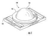
- FIG. 1is a top perspective view of a light emitting device package according to an embodiment of the subject matter described herein;
- FIG. 2is a top plan view of the light emitting device package shown in FIG. 1 ;
- FIG. 3is a side plan view of the light emitting device package shown in FIGS. 2 and 3 ;
- FIG. 4Ais a cross-sectional side view of the light emitting device package shown in FIGS. 1-3 ;
- FIG. 4Bis a cross-sectional side view of an assembly step of the light emitting device package shown in FIG. 4A ;
- FIG. 4Cis a cross-sectional side view of another assembly step of the light emitting device package shown in FIG. 4A ;
- FIG. 5is a top plan view of a substrate, a lens coupler, and a light emitting device assembly according to an embodiment of the subject matter described herein;
- FIG. 6is an exploded perspective view of a light emitting device package according to an embodiment of the subject matter described herein;
- FIG. 7is a bottom plan view of a substrate according to an embodiment of the subject matter described herein.
- FIGS. 8A-8Gare cross-sectional side view of a light emitting device package showing alternative embodiments of a lens coupler.
- FIGS. 1-8GLight emitting device packages, LED packages and related methods are described herein with reference to FIGS. 1-8G , which illustrate various embodiments. As illustrated in the Figures, some sizes of structures or portions may be exaggerated relative to other structures or portions for illustrative purposes and, thus, are provided to illustrate the general structures of the subject matter disclosed herein. Further, various aspects of the subject matter disclosed herein are described with reference to a structure or a portion being formed on other structures, portions, or both. As will be appreciated by those of skill in the art, references to a structure being formed “on” or “above” another structure or portions contemplates that additional structure, portion, or both may intervene. References to a structure or a portion being formed “on” another structure or portion without an intervening structure or portion are described herein as being formed “directly on” the structure or portion.
- relative terms such as “on” or “above”are used herein to describe one structure's or portion's relationship to another structure or portion as illustrated in the Figures. It will be understood that relative terms such as “on” or “above” are intended to encompass different orientations of the device in addition to the orientation depicted in the Figures. For example, if the device in the Figures is turned over, structure or portion described as “above” other structures or portions would now be oriented “below” the other structures or portions. Likewise, if the device in the Figures is rotated along an axis, structure or portion described as “above” other structures or portions would now be oriented “next to” or “left of” the other structures or portions. Like numbers refer to like elements throughout.
- a light emitting device packageincludes a mounting pad adapted for attachment of a light emitting device.
- a lens coupleris attached to the mounting pad and defines an opening for containing the light emitting device and a quantity of at least partially cured encapsulant.
- the lens couplerincludes a surface defining a depression which comprises at least one edge that substantially surrounds an open end of the opening and that shapes the encapsulant into a convex meniscus.
- the packagemay include a lens positioned to substantially enclose the opening and to interface with the convex meniscus of the encapsulant.
- an LED packageincludes a substrate including a mounting pad.
- An LEDmay be attached to the mounting pad.
- a lens couplermay be attached to the mounting pad and define an opening for containing the LED and a first quantity of encapsulant.
- the lens couplerincludes at least one surface defining a first depression which comprises a first edge that substantially surrounds an open end of the opening and that shapes the first quantity of encapsulant into a first convex meniscus.
- the surfacedefines a second depression which comprises a second edge that substantially surrounds the first edge and shapes a second quantity of encapsulant into a second convex meniscus.
- a lensmay be positioned to substantially enclose the opening and to interface with the convex meniscus of the encapsulant.
- the term “light emitting device”may include an LED, laser diode, and/or other semiconductor device which includes one or more semiconductor layers, which may include silicon, silicon carbide, gallium nitride and/or other semiconductor materials, a substrate which may include sapphire, silicon, silicon carbide and/or other microelectronic substrates, and one or more contact layers which may include metal and/or other conductive layers.
- semiconductor light emitting devicesmay be gallium nitride-based LEDs or lasers fabricated on a silicon carbide substrate such as those devices manufactured and sold by Cree, Inc. of Durham, N.C., although other emitting devices from other material systems may also be used.
- an encapsulantmay include any suitable transparent or semitransparent material for adhering objects together.
- an encapsulantcan be a liquid silicone gel or epoxy-based material.
- the encapsulantmay contain one or more of oxide particles, silicates, nanoparticles, light scattering particles, light diffusing particles, color filtering material, and phosphors of the same or different type.
- FIGS. 1 , 2 and 3are a top perspective view, a top plan view, and a side plan view, respectively, of a light emitting device package, generally designated 100 , according to an embodiment of the subject matter described herein.
- package 100includes a substrate 102 , a lens 104 , and a lens coupler 106 .
- Lens coupler 106can be adapted for attachment to substrate 102 and for placement of lens 104 in an operable position with respect to a light emitting device, which is attached to substrate 102 .
- the operable positioncan include positions at which light emitted by a light emitting device attached to substrate 102 can transmit through lens 104 .
- lens coupler 106can be structured, as described in more detail hereinbelow, to align a center of lens 104 along a vertical axis with the light emitting device.
- Lens 104may be made from material having high light transmissivity such as, for example only, glass, quartz, high temperature and transparent plastic, or a combination of these materials.
- the lensmay define a recess in the bottom thereof having a curved, hemispherical, or other geometry, which can be filled with optical materials intended to influence or change the nature of the light emitted by a light emitting device in package 100 .
- optical materialsinclude luminescence converting phosphors, dyes, fluorescent polymers or other materials which absorb some of the light emitted by the light emitting device and re-emit light of different wavelengths.
- Examples of another type of optical materialare light diffusants such as calcium carbonate, scattering particles (such as titanium oxides) or voids which disperse or scatter light. Any single or combination of the above materials can be applied on the lens to obtain certain spectral luminous performance.
- Substrate 102may be formed of many different materials, including electrically insulating materials. Suitable substrate materials include, but are not limited to, ceramic materials such as aluminum nitride (AlN) and alumina (Al 2 O 3 ). Dimensions of substrate 102 can vary widely depending on application and processes used to manufacture package 100 . For example, in the illustrated embodiment, substrate 102 may have dimensions ranging from fractions of millimeters (mm) to tens of millimeters.
- Lens coupler 106may be disk-shaped or any other suitable shape and formed of a durable, high melting temperature material that can withstand subsequent packaging manufacturing steps and the heat generated by the package during operation. Many different materials can be used, including plastics, such as a Novella resin, or liquid crystal polymers. Lens coupler 106 may be made of a material that reflects and/or scatters light.
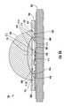
- FIG. 4Ais a cross-sectional side view of package 100 shown in FIGS. 1-3 .
- a semiconductor light emitting device assemblygenerally designated 108
- Assembly 108can include an LED 110 , which may be mounted to a mounting pad 109 .
- Mounting pad 109may be mounted to substrate 102 with electrical connections being made to LED 110 for applying an electrical bias.
- a top surface of LED 110may be connected to electrical connections via one or more conductive bond wires 112 .
- Lens coupler 106can include reflective surfaces positioned to reflect light generated by LED 110 . Particularly, the reflective surfaces can be positioned for directing the light upwardly and away from package 100 so that it can contribute to useful light emission of package 100 . Further, lens coupler 106 can have many different shapes and sizes and to enhance its reflectivity, may include a reflective element covering different portions of the coupler surface around LED 110 . Alternatively, lens coupler 106 can be made of a reflective material such that light from LED 110 directed toward the surfaces of coupler 106 is reflected to contribute to package emission.
- Lens 104may be attached to substrate 102 and lens coupler 106 by use of an encapsulant 111 .
- encapsulant 111may be deposited in a space 400 defined between substrate 102 , lens 104 , and/or lens coupler 106 .
- Encapsulant 111may be any suitable type of resin material such as a silicone or epoxy-based material.
- the volume of encapsulant 111may be kept at a minimum such that assembly 108 is positioned within space 400 and such that lens 104 is securely attached to substrate 102 . Further, the distance of the spacing between substrate 102 and lens 104 may be kept at a minimum such that the vertical movement of lens 104 is at a minimum over the operating temperature ranges of package 100 .
- lens 104only moves up by a few microns at a high operating temperature. Further, the distance between substrate 102 and lens 104 can be less than about 100 ⁇ m.
- Lens 104can be placed on top of and adhere to encapsulant 111 .
- Lens 104is not rigidly bonded to lens coupler 106 .
- This “floating lens” designwill ensure that encapsulant 111 can expand and contract under high and low temperature conditions without problem. For instance, when package 100 is operating or being subjected to a high temperature environment, encapsulant 111 experiences greater volumetric expansion than the cavity space that contains it. By allowing lens 104 to float somewhat freely on top of encapsulant 104 , no encapsulant will be squeezed out of its cavity space. Likewise, when package is subjected to cold temperature, encapsulant 111 will contract more than the other components that make up the cavity space for encapsulant 111 .
- Lens 104will float freely on top of encapsulant 111 as the latter shrinks and its level drops. Hence, the reliability of package 100 is maintained over a relatively large temperature range as the thermal stresses induced on its encapsulant 111 is reduced by the floating lens design.
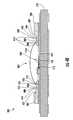
- FIG. 4Bis a cross-sectional side view of package 100 at an assembly step when a first quantity of encapsulant 111 A is deposited within an opening, generally designated 402 , defined by the attachment of lens coupler 106 to mounting pad 109 .
- encapsulant 111 Ais deposited in an opening 402 .
- Opening 402can include an open end into which encapsulant 111 A is deposited.
- the open end of opening 402is defined by ledge surface 404 of lens coupler 106 , which surrounds the open end of opening 402 .
- Lens coupler 106includes a ledge surface 404 that substantially surrounds the open end of opening 402 .
- Ledge surface 404defines first and second depressions 406 and 408 , which substantially surround the open end.
- Depressions 406 and 408include edges 410 formed at an interface of surface 404 and the depressions.
- Opening 402is filled with encapsulant 111 A until the encapsulant 111 A forms a convex meniscus, which is formed by an edge of depression 406 .
- Depression 406can entirely or at least substantially surround the open end of opening 402 (see also FIGS. 5 and 6 ). Further, edges 410 of depression 406 can entirely or at least substantially surround the open end of opening 402 .
- encapsulant 111 Acan be partially or fully cured. For example, the encapsulant may be cured to about 50%.
- Depressions 406 and 408can have any suitable size and shape for forming an outer surface of encapsulant 111 A.
- the depressioncan have substantially vertical walls such that a convex meniscus is formed by encapsulant 111 A when opening 402 is filled with encapsulant 111 A.
- a vertical wall of depressions 406 and 408can be about 90° with respect to ledge surface 404 .
- a wall of depressions 406 and 408can be inclined in the range of between about 60° and about 90° with respect to ledge surface 404 .
- the width and depth of depressions 406 and 408can range between 5 and 10 mils, although the depressions may have any other suitable depth or width.
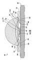
- FIG. 4Cis a cross-sectional side view of package 100 at an assembly step when a second quantity of encapsulant 111 B is deposited within opening 402 .
- encapsulant 111 Bcan be deposited directly on encapsulant 111 A.
- encapsulant 111 Bcan cover encapsulant 111 B and form a convex meniscus.
- the convex meniscus of encapsulant 111 Bcan be formed by one of the edges of depression 408 .
- Depression 408can entirely or at least substantially surround the open end of opening 402 (see also FIGS. 5 and 6 ). Further, edges 410 of depression 408 can entirely or at least substantially surround the open end of opening 402 .
- Encapsulant 111 Bmay be uncured or partially cured. Encapsulant 111 B can be deposited in an amount such that the encapsulant does not overflow guide surfaces 407 of opening 402 when a lens is positioned on top of the encapsulant. Surfaces 404 and 407 may be reflective for reflecting light generated by LED 110 in a substantially upward direction. Alternatively, surfaces 404 and 407 may be non-reflective.
- encapsulant 111 A and 111 Bcan form encapsulant 111 shown in FIG. 4A .
- Encapsulant 111 Ais substantially or entirely cured such that it remains in a form with a convex meniscus even after placement of lens 104 .
- Lens 104includes a concave surface 113 in the bottom thereof that substantially conforms to a surface of the convex meniscus of encapsulant 111 A.
- Encapsulant 111 Bis left uncured or only partially cured such that lens 104 “rests” or “floats” on encapsulant 111 B after placement. As shown in FIG. 4A , encapsulant 111 B spreads laterally and over ledge surface 404 after placement of lens 104 .
- lens 104may include a flat surface 115 (shown to be coplanar with the top surface of encapsulant 111 B) that is positioned to face the encapsulant and LED 110 .
- Lens 104is substantially hemispherical in shape, and the flat surface of lens 104 is facing the encapsulant and LED 110 .
- at least a portion of the top surface of encapsulant 111 Amay substantially conform to flat surface 115 .
- the top surface of encapsulant 111 Ais lower than the position indicated by reference numeral 111 A and at the position indicated by reference numeral 111 C.
- the forming separate forming of encapsulant portions 111 A and 111 B as described hereinserves to minimize or prevent the formation of voids within encapsulant 111 .
- the formation of voidsis minimized or prevented by placement of lens 104 onto encapsulant portions 111 A and 111 B.
- a bottom surface of lens 104is positioned to interface with the top surface of encapsulant 111 A.
- encapsulant 111 Bis forced from between lens 104 and encapsulant 111 A to rest on top of ledge surface 404 along the outer edge of encapsulant 111 A.
- the outside edge of lens 104interfaces with encapsulant 111 B.
- encapsulant 111 Bis forced from between lens 104 and encapsulant 111 A, bubble formation is minimized or prevented in the areas where light passes through encapsulant 111 . As a result of reduced bubbles in these areas, the quality of light produced by light emitting device package 100 is improved.
- Lens coupler 106may be adapted to precisely align lens 104 with LED 110 during assembly.
- Lens coupler 106may include one or more top surfaces that are shaped to substantially fit to a bottom portion of lens 104 and function as a guide for aligning lens 104 into its operational position with respect to LED 110 .
- ledge surface 404may substantially fit to an outside edge of a bottom surface of lens 104 .
- LED 110is substantially aligned with lens 104 .
- lens coupler 106may include one or more guide surfaces 407 adapted for guiding the movement of lens 104 into its operational position during assembly. Guide surface 407 can be substantially funnel shaped for precisely positioning the outside edge of bottom surface 404 against ledge surface 404 .
- FIG. 5is a top plan view of substrate 102 , lens coupler 106 , and light emitting device assembly 108 .
- substrate 102includes a top surface 500 having electrical traces 502 and mounting pad 109 .
- LED 110can be mounted to mounting pad 109 .
- Electrical traces 502provide a conductive path for electrical connection of LED 110 .
- Mounting pad 109covers a portion of top surface 500 and a portion of electrical traces 502 . Further, mounting pad 109 can be located near or at the center of top surface 500 or at any other suitable location on surface 500 .
- Electrical traces 502can provide electrical connection to LED 110 either through a submount or by bond wires 112 .
- Depressions 406 and 408are each substantially shaped as circles that surround opening 402 , which leads to assembly 108 . Particularly, depressions 406 and 408 form circles having LED 110 positioned at a common center. Edges 410 of depressions 406 and 408 also substantially surround opening 402 , which leads to assembly 108 .
- FIG. 6is an exploded perspective view of light emitting device package 100 .
- a quantity of epoxy 600can attach lens coupler 106 to substrate 102 .
- any other suitable adhesive or attachment techniquemay be utilized for attaching lens coupler 106 to substrate 102 .
- FIG. 7is a bottom plan view of substrate 102 .
- conductive portions 702can be attached to a bottom surface 702 of substrate 102 .
- Conductive portions 702may be made of any suitable metal.
- conductive portions 702may be connected to the electrical traces on the top surface of substrate 102 for providing electrical connection of LED 110 to an underside of substrate 102 .
- Apertures or vias 704may be formed through substrate 102 and include electrical traces having conductive paths for connecting the electrical traces on the top surface of substrate 102 to conductive portions 702 .
- FIGS. 8A-8Gillustrate alternative embodiments of lens coupler 106 .
- depressions 406 and 408are triangular in shape.
- depressions 406 and 408are square shaped. Depressions 406 and 408 may be any other suitable shape having at least one edge that shapes an outer surface of the encapsulant.
- ledge surface 404is inclined with respect to the top surface of substrate 102 .
- surface 404includes a portion 404 a that is substantially parallel to the top surface of substrate 102 .
- Depressions 406are formed in surface portion 404 a .
- Surface 404also includes a portion 404 b that is inclined with respect to the top surface of substrate 102 .
- Depressions 408are formed in surface portion 404 b .
- depressions 408are in a raised position with respect to depressions 406 .
- depressions 406 and 408are circular or curved in shape, although the depressions may alternatively be any other suitable shape.
- depressions 408are in a raised position with respect to depressions 406 .
- depressions 406 and 408are triangular in shape, although the depressions may alternatively be any other suitable shape.
- depressions 406 and 408are formed in inclined surface portion 404 b . As a result, depressions 408 are in a raised position with respect to depressions 406 . Further, depressions 406 and 408 are triangular in shape, although the depressions may alternatively be any other suitable shape.
- surface 404includes a stepped structure. Depressions 406 and 408 are formed in different “steps” of surface 404 . As a result, depressions 408 are in a raised position with respect to depressions 406 . Although depressions 406 and 408 are circular or curved in shape, the depressions may alternatively be any other suitable shape.
- lens coupler 106includes depressions 800 and 802 formed within an underside of the lens coupler.
- a suitable encapsulantcan be disposed in depressions 800 and 802 for adhering lens coupler 106 to substrate 102 .
- Depressions 800 and 802may be any suitable shape and size for enclosing the encapsulant.
- a plurality of the light emitting device packages as disclosed hereincan be arranged together one or more substrates. Further, the packages can be operably connected to suitable circuitry for providing power and control to the LEDs.
Landscapes
- Led Device Packages (AREA)
Abstract
Description
Claims (25)
Priority Applications (1)
| Application Number | Priority Date | Filing Date | Title |
|---|---|---|---|
| US11/895,795US7939842B2 (en) | 2005-01-27 | 2007-08-27 | Light emitting device packages, light emitting diode (LED) packages and related methods |
Applications Claiming Priority (2)
| Application Number | Priority Date | Filing Date | Title |
|---|---|---|---|
| US11/044,779US7326583B2 (en) | 2004-03-31 | 2005-01-27 | Methods for packaging of a semiconductor light emitting device |
| US11/895,795US7939842B2 (en) | 2005-01-27 | 2007-08-27 | Light emitting device packages, light emitting diode (LED) packages and related methods |
Related Parent Applications (1)
| Application Number | Title | Priority Date | Filing Date |
|---|---|---|---|
| US11/044,779Continuation-In-PartUS7326583B2 (en) | 2004-03-31 | 2005-01-27 | Methods for packaging of a semiconductor light emitting device |
Publications (2)
| Publication Number | Publication Date |
|---|---|
| US20080054286A1 US20080054286A1 (en) | 2008-03-06 |
| US7939842B2true US7939842B2 (en) | 2011-05-10 |
Family
ID=39150246
Family Applications (1)
| Application Number | Title | Priority Date | Filing Date |
|---|---|---|---|
| US11/895,795Active2027-01-11US7939842B2 (en) | 2005-01-27 | 2007-08-27 | Light emitting device packages, light emitting diode (LED) packages and related methods |
Country Status (1)
| Country | Link |
|---|---|
| US (1) | US7939842B2 (en) |
Cited By (4)
| Publication number | Priority date | Publication date | Assignee | Title |
|---|---|---|---|---|
| US20100067240A1 (en)* | 2008-09-16 | 2010-03-18 | John Selverian | Optical Cup For Lighting Module |
| US20190305196A1 (en)* | 2018-03-30 | 2019-10-03 | Nichia Corporation | Light emitting device |
| US20220359802A1 (en)* | 2018-02-26 | 2022-11-10 | Semicon Light Co., Ltd. | Semiconductor light emitting devices and method of manufacturing the same |
| US12191427B2 (en)* | 2018-02-05 | 2025-01-07 | Lg Innotek Co., Ltd. | Semiconductor device package and light emitting device comprising same |
Families Citing this family (60)
| Publication number | Priority date | Publication date | Assignee | Title |
|---|---|---|---|---|
| USD591697S1 (en) | 2006-08-09 | 2009-05-05 | Cree, Inc. | Lamp package |
| USD598871S1 (en)* | 2006-11-06 | 2009-08-25 | Koninklijke Philips Electronics N.V. Et Al. | LED package |
| US8638219B2 (en)* | 2007-06-18 | 2014-01-28 | Qualcomm Incorporated | Device and methods of providing radio data system information alerts |
| US9172012B2 (en) | 2007-10-31 | 2015-10-27 | Cree, Inc. | Multi-chip light emitter packages and related methods |
| US9082921B2 (en) | 2007-10-31 | 2015-07-14 | Cree, Inc. | Multi-die LED package |
| US9666762B2 (en) | 2007-10-31 | 2017-05-30 | Cree, Inc. | Multi-chip light emitter packages and related methods |
| KR101526567B1 (en)* | 2008-05-07 | 2015-06-10 | 엘지이노텍 주식회사 | Lighting emitting diode package |
| KR101629654B1 (en)* | 2008-12-19 | 2016-06-13 | 삼성전자주식회사 | Light emitting device package, backlight unit, display device and illumination device |
| US8096671B1 (en) | 2009-04-06 | 2012-01-17 | Nmera, Llc | Light emitting diode illumination system |
| DE102009031008A1 (en)* | 2009-06-29 | 2010-12-30 | Osram Opto Semiconductors Gmbh | Optoelectronic component |
| TWD139671S1 (en)* | 2009-09-25 | 2011-03-21 | 億光電子工業股份有限公司 | Light emitting diode lamp |
| USD630171S1 (en)* | 2009-10-16 | 2011-01-04 | Everlight Electronics Co., Ltd. | Light emitting diode |
| USD643381S1 (en)* | 2010-04-07 | 2011-08-16 | Everlight Electronics Co., Ltd. | Light emitting diode |
| USD629368S1 (en)* | 2010-04-07 | 2010-12-21 | Everlight Electronics Co., Ltd. | Light emitting diode |
| USD640643S1 (en)* | 2010-04-07 | 2011-06-28 | Everlight Electronics Co., Ltd. | Light emitting diode |
| US8492777B2 (en) | 2010-04-09 | 2013-07-23 | Everlight Electronics Co., Ltd. | Light emitting diode package, lighting device and light emitting diode package substrate |
| USD651989S1 (en) | 2010-04-09 | 2012-01-10 | Everlight Electronics Co., Ltd. | Light emitting diode |
| USD631020S1 (en)* | 2010-04-29 | 2011-01-18 | Edison Opto Corporation | LED package |
| WO2011137361A1 (en)* | 2010-04-30 | 2011-11-03 | Uniflux Led. Inc. | A sealed structure of led road/street light |
| SG10201504616TA (en)* | 2010-06-11 | 2015-07-30 | Ricoh Co Ltd | Information storage device, removable device, developer container, and image forming apparatus |
| USD634718S1 (en)* | 2010-06-30 | 2011-03-22 | Edison Opto Corporation | LED package |
| TWD141204S1 (en) | 2010-07-23 | 2011-06-21 | 億光電子工業股份有限公司 | Light emitting diode |
| USD712850S1 (en) | 2010-11-18 | 2014-09-09 | Cree, Inc. | Light emitter device |
| US8564000B2 (en) | 2010-11-22 | 2013-10-22 | Cree, Inc. | Light emitting devices for light emitting diodes (LEDs) |
| USD676000S1 (en)* | 2010-11-22 | 2013-02-12 | Cree, Inc. | Light emitting device package |
| USD721339S1 (en) | 2010-12-03 | 2015-01-20 | Cree, Inc. | Light emitter device |
| USD707192S1 (en) | 2010-11-18 | 2014-06-17 | Cree, Inc. | Light emitting device |
| US9300062B2 (en) | 2010-11-22 | 2016-03-29 | Cree, Inc. | Attachment devices and methods for light emitting devices |
| US8575639B2 (en) | 2011-02-16 | 2013-11-05 | Cree, Inc. | Light emitting devices for light emitting diodes (LEDs) |
| USD650760S1 (en)* | 2010-11-22 | 2011-12-20 | Cree, Inc. | Light emitting device package |
| US9490235B2 (en) | 2010-11-22 | 2016-11-08 | Cree, Inc. | Light emitting devices, systems, and methods |
| US9000470B2 (en) | 2010-11-22 | 2015-04-07 | Cree, Inc. | Light emitter devices |
| US8624271B2 (en) | 2010-11-22 | 2014-01-07 | Cree, Inc. | Light emitting devices |
| USD706231S1 (en) | 2010-12-03 | 2014-06-03 | Cree, Inc. | Light emitting device |
| USD702653S1 (en) | 2011-10-26 | 2014-04-15 | Cree, Inc. | Light emitting device component |
| US8809880B2 (en) | 2011-02-16 | 2014-08-19 | Cree, Inc. | Light emitting diode (LED) chips and devices for providing failure mitigation in LED arrays |
| US8455908B2 (en) | 2011-02-16 | 2013-06-04 | Cree, Inc. | Light emitting devices |
| USD705181S1 (en) | 2011-10-26 | 2014-05-20 | Cree, Inc. | Light emitting device component |
| KR20140097284A (en) | 2011-11-07 | 2014-08-06 | 크리,인코포레이티드 | High voltage array light emitting diode(led) devices, fixtures and methods |
| US10043960B2 (en)* | 2011-11-15 | 2018-08-07 | Cree, Inc. | Light emitting diode (LED) packages and related methods |
| TWD152154S (en)* | 2012-03-14 | 2013-03-01 | 華新麗華股份有限公司 | Lens for light emitting diode |
| US9735198B2 (en) | 2012-03-30 | 2017-08-15 | Cree, Inc. | Substrate based light emitter devices, components, and related methods |
| US10134961B2 (en) | 2012-03-30 | 2018-11-20 | Cree, Inc. | Submount based surface mount device (SMD) light emitter components and methods |
| USD703624S1 (en)* | 2012-04-06 | 2014-04-29 | Cree, Inc. | LED-array package |
| US9515055B2 (en) | 2012-05-14 | 2016-12-06 | Cree, Inc. | Light emitting devices including multiple anodes and cathodes |
| USD709464S1 (en)* | 2012-05-31 | 2014-07-22 | Cree, Inc. | Light emitting diode (LED) package |
| US9349929B2 (en) | 2012-05-31 | 2016-05-24 | Cree, Inc. | Light emitter packages, systems, and methods |
| USD749051S1 (en)* | 2012-05-31 | 2016-02-09 | Cree, Inc. | Light emitting diode (LED) package |
| US10439112B2 (en) | 2012-05-31 | 2019-10-08 | Cree, Inc. | Light emitter packages, systems, and methods having improved performance |
| USD711841S1 (en)* | 2012-08-23 | 2014-08-26 | Cree, Inc. | Light emitting diode (LED) package |
| USD679443S1 (en)* | 2012-09-05 | 2013-04-02 | Foshan Innovative Lighting Co., Ltd. | Light module |
| US9345091B2 (en) | 2013-02-08 | 2016-05-17 | Cree, Inc. | Light emitting device (LED) light fixture control systems and related methods |
| USD739565S1 (en) | 2013-06-27 | 2015-09-22 | Cree, Inc. | Light emitter unit |
| USD740453S1 (en) | 2013-06-27 | 2015-10-06 | Cree, Inc. | Light emitter unit |
| DE102014215940A1 (en)* | 2014-08-12 | 2016-02-18 | Osram Gmbh | Producing a lighting device |
| USD823492S1 (en) | 2016-10-04 | 2018-07-17 | Cree, Inc. | Light emitting device |
| JP1618491S (en)* | 2017-11-21 | 2018-11-19 | ||
| USD871485S1 (en)* | 2018-01-15 | 2019-12-31 | Axis Ab | Camera |
| JP1628923S (en)* | 2018-04-26 | 2019-04-08 | ||
| CN116053386B (en)* | 2023-02-04 | 2025-09-09 | 深圳市卓越华予电路有限公司 | Light emitting chip packaging structure and packaging method |
Citations (50)
| Publication number | Priority date | Publication date | Assignee | Title |
|---|---|---|---|---|
| US3875456A (en) | 1972-04-04 | 1975-04-01 | Hitachi Ltd | Multi-color semiconductor lamp |
| US4918497A (en) | 1988-12-14 | 1990-04-17 | Cree Research, Inc. | Blue light emitting diode formed in silicon carbide |
| US4966862A (en) | 1989-08-28 | 1990-10-30 | Cree Research, Inc. | Method of production of light emitting diodes |
| US5027168A (en) | 1988-12-14 | 1991-06-25 | Cree Research, Inc. | Blue light emitting diode formed in silicon carbide |
| US5043716A (en) | 1988-07-14 | 1991-08-27 | Adaptive Micro Systems, Inc. | Electronic display with lens matrix |
| US5210051A (en) | 1990-03-27 | 1993-05-11 | Cree Research, Inc. | High efficiency light emitting diodes from bipolar gallium nitride |
| US5338944A (en) | 1993-09-22 | 1994-08-16 | Cree Research, Inc. | Blue light-emitting diode with degenerate junction structure |
| US5393993A (en) | 1993-12-13 | 1995-02-28 | Cree Research, Inc. | Buffer structure between silicon carbide and gallium nitride and resulting semiconductor devices |
| US5416342A (en) | 1993-06-23 | 1995-05-16 | Cree Research, Inc. | Blue light-emitting diode with high external quantum efficiency |
| JPH0832120A (en) | 1994-07-19 | 1996-02-02 | Rohm Co Ltd | Surface emission type display |
| US5523589A (en) | 1994-09-20 | 1996-06-04 | Cree Research, Inc. | Vertical geometry light emitting diode with group III nitride active layer and extended lifetime |
| JPH0927643A (en) | 1995-07-13 | 1997-01-28 | Stanley Electric Co Ltd | Light receiving / light emitting element |
| US5604135A (en) | 1994-08-12 | 1997-02-18 | Cree Research, Inc. | Method of forming green light emitting diode in silicon carbide |
| US5631190A (en) | 1994-10-07 | 1997-05-20 | Cree Research, Inc. | Method for producing high efficiency light-emitting diodes and resulting diode structures |
| JPH1065220A (en) | 1996-08-23 | 1998-03-06 | Sharp Corp | Semiconductor light emitting device and method of manufacturing the same |
| US5739554A (en) | 1995-05-08 | 1998-04-14 | Cree Research, Inc. | Double heterojunction light emitting diode with gallium nitride active layer |
| JPH10190065A (en) | 1996-12-27 | 1998-07-21 | Nichia Chem Ind Ltd | Light emitting device and LED display using the same |
| US5959316A (en) | 1998-09-01 | 1999-09-28 | Hewlett-Packard Company | Multiple encapsulation of phosphor-LED devices |
| JP2000252523A (en) | 1999-02-25 | 2000-09-14 | Nichia Chem Ind Ltd | Method of forming light emitting diode |
| US6187606B1 (en) | 1997-10-07 | 2001-02-13 | Cree, Inc. | Group III nitride photonic devices on silicon carbide substrates with conductive buffer interlayer structure |
| WO2001015242A1 (en) | 1999-08-25 | 2001-03-01 | Osram Opto Semiconductors Gmbh & Co. Ohg | Method for the production of an optoelectronic component with a lens |
| US6274890B1 (en) | 1997-01-15 | 2001-08-14 | Kabushiki Kaisha Toshiba | Semiconductor light emitting device and its manufacturing method |
| US20010030326A1 (en) | 1996-06-26 | 2001-10-18 | Osram Opto Semiconductors Gmbh & Co. Ohg, A Germany Corporation | Light-radiating semiconductor component with a luminescence conversion element |
| EP1187226A1 (en) | 2000-09-01 | 2002-03-13 | Citizen Electronics Co., Ltd. | Surface-mount type light emitting diode and method of manufacturing same |
| US20020057056A1 (en) | 2000-08-09 | 2002-05-16 | Tadahiro Okazaki | Light-emitting diode |
| US20020079837A1 (en) | 2000-12-19 | 2002-06-27 | Jun Okazaki | Chip-type LED and process of manufacturing the same |
| US20020123164A1 (en) | 2001-02-01 | 2002-09-05 | Slater David B. | Light emitting diodes including modifications for light extraction and manufacturing methods therefor |
| DE10109349A1 (en) | 2001-02-27 | 2002-09-12 | Osram Opto Semiconductors Gmbh | Radiation-emitting semiconductor component comprises radiation-producing semiconductor body, radiation-permeable plastic element and radiation converter |
| US20020163001A1 (en) | 2001-05-04 | 2002-11-07 | Shaddock David Mulford | Surface mount light emitting device package and fabrication method |
| US20030006418A1 (en) | 2001-05-30 | 2003-01-09 | Emerson David Todd | Group III nitride based light emitting diode structures with a quantum well and superlattice, group III nitride based quantum well structures and group III nitride based superlattice structures |
| US20030141510A1 (en) | 2000-04-26 | 2003-07-31 | Osram Opto Semiconductors Gmbh | Radiation emitting semiconductor component with luminescent conversion element |
| US6610563B1 (en) | 1997-12-15 | 2003-08-26 | Osram Opto Semiconductors Gmbh & Co. Ohg | Surface mounting optoelectronic component and method for producing same |
| US6635363B1 (en) | 2000-08-21 | 2003-10-21 | General Electric Company | Phosphor coating with self-adjusting distance from LED chip |
| US6642652B2 (en) | 2001-06-11 | 2003-11-04 | Lumileds Lighting U.S., Llc | Phosphor-converted light emitting device |
| US20030211804A1 (en) | 1999-04-22 | 2003-11-13 | Osram Opto Semiconductors Gmbh & Co. Ohg | LED light source with lens and corresponding production method |
| US20040041222A1 (en) | 2002-09-04 | 2004-03-04 | Loh Ban P. | Power surface mount light emitting die package |
| US20040056260A1 (en) | 2002-09-19 | 2004-03-25 | Slater David B. | Phosphor-coated light emitting diodes including tapered sidewalls, and fabrication methods therefor |
| US6744077B2 (en) | 2002-09-27 | 2004-06-01 | Lumileds Lighting U.S., Llc | Selective filtering of wavelength-converted semiconductor light emitting devices |
| US6747406B1 (en) | 2000-08-07 | 2004-06-08 | General Electric Company | LED cross-linkable phospor coating |
| US20040126913A1 (en) | 2002-12-06 | 2004-07-01 | Loh Ban P. | Composite leadframe LED package and method of making the same |
| US6765801B1 (en) | 2001-06-25 | 2004-07-20 | Amkor Technology, Inc. | Optical track drain package |
| WO2004068594A1 (en) | 2003-01-30 | 2004-08-12 | Osram Opto Semiconductors Gmbh | Semiconductor component emitting and/or receiving electromagnetic radiation, and housing base for such a component |
| JP2005197369A (en) | 2004-01-05 | 2005-07-21 | Toshiba Corp | Optical semiconductor device |
| US20050221518A1 (en) | 2004-03-31 | 2005-10-06 | Peter Andrews | Reflector packages and methods for packaging of a semiconductor light emitting device |
| US6953952B2 (en) | 2002-09-05 | 2005-10-11 | Nichia Corporation | Semiconductor device and an optical device using the semiconductor device |
| WO2005098975A2 (en) | 2004-03-31 | 2005-10-20 | Cree, Inc. | Methods for packaging a light emitting device and packaged light emitting devices |
| WO2005098976A2 (en) | 2004-03-31 | 2005-10-20 | Cree, Inc. | Semiconductor light emitting devices including a luminescent conversion element and methods for packaging the same |
| US7078254B2 (en) | 2002-12-06 | 2006-07-18 | Cree, Inc. | LED package die having a small footprint |
| US20060186423A1 (en) | 2003-05-05 | 2006-08-24 | Greg Blonder | Method of making optical light engines with elevated LEDs and resulting product |
| US20060278882A1 (en) | 2005-06-10 | 2006-12-14 | Cree, Inc. | Power lamp package |
Family Cites Families (1)
| Publication number | Priority date | Publication date | Assignee | Title |
|---|---|---|---|---|
| US4966882A (en)* | 1987-06-05 | 1990-10-30 | Babcock-Hitachi Kabushiki Kaisha | Catalyst for denitration by catalytic reduction using ammonia and a process for producing the same |
- 2007
- 2007-08-27USUS11/895,795patent/US7939842B2/enactiveActive
Patent Citations (59)
| Publication number | Priority date | Publication date | Assignee | Title |
|---|---|---|---|---|
| US3875456A (en) | 1972-04-04 | 1975-04-01 | Hitachi Ltd | Multi-color semiconductor lamp |
| US5043716A (en) | 1988-07-14 | 1991-08-27 | Adaptive Micro Systems, Inc. | Electronic display with lens matrix |
| US4918497A (en) | 1988-12-14 | 1990-04-17 | Cree Research, Inc. | Blue light emitting diode formed in silicon carbide |
| US5027168A (en) | 1988-12-14 | 1991-06-25 | Cree Research, Inc. | Blue light emitting diode formed in silicon carbide |
| US4966862A (en) | 1989-08-28 | 1990-10-30 | Cree Research, Inc. | Method of production of light emitting diodes |
| US5210051A (en) | 1990-03-27 | 1993-05-11 | Cree Research, Inc. | High efficiency light emitting diodes from bipolar gallium nitride |
| US5416342A (en) | 1993-06-23 | 1995-05-16 | Cree Research, Inc. | Blue light-emitting diode with high external quantum efficiency |
| US5338944A (en) | 1993-09-22 | 1994-08-16 | Cree Research, Inc. | Blue light-emitting diode with degenerate junction structure |
| US5393993A (en) | 1993-12-13 | 1995-02-28 | Cree Research, Inc. | Buffer structure between silicon carbide and gallium nitride and resulting semiconductor devices |
| JPH0832120A (en) | 1994-07-19 | 1996-02-02 | Rohm Co Ltd | Surface emission type display |
| US5604135A (en) | 1994-08-12 | 1997-02-18 | Cree Research, Inc. | Method of forming green light emitting diode in silicon carbide |
| US5523589A (en) | 1994-09-20 | 1996-06-04 | Cree Research, Inc. | Vertical geometry light emitting diode with group III nitride active layer and extended lifetime |
| US5912477A (en) | 1994-10-07 | 1999-06-15 | Cree Research, Inc. | High efficiency light emitting diodes |
| US5631190A (en) | 1994-10-07 | 1997-05-20 | Cree Research, Inc. | Method for producing high efficiency light-emitting diodes and resulting diode structures |
| US6120600A (en) | 1995-05-08 | 2000-09-19 | Cree, Inc. | Double heterojunction light emitting diode with gallium nitride active layer |
| US5739554A (en) | 1995-05-08 | 1998-04-14 | Cree Research, Inc. | Double heterojunction light emitting diode with gallium nitride active layer |
| JPH0927643A (en) | 1995-07-13 | 1997-01-28 | Stanley Electric Co Ltd | Light receiving / light emitting element |
| US20010030326A1 (en) | 1996-06-26 | 2001-10-18 | Osram Opto Semiconductors Gmbh & Co. Ohg, A Germany Corporation | Light-radiating semiconductor component with a luminescence conversion element |
| JPH1065220A (en) | 1996-08-23 | 1998-03-06 | Sharp Corp | Semiconductor light emitting device and method of manufacturing the same |
| JPH10190065A (en) | 1996-12-27 | 1998-07-21 | Nichia Chem Ind Ltd | Light emitting device and LED display using the same |
| US6274890B1 (en) | 1997-01-15 | 2001-08-14 | Kabushiki Kaisha Toshiba | Semiconductor light emitting device and its manufacturing method |
| US6187606B1 (en) | 1997-10-07 | 2001-02-13 | Cree, Inc. | Group III nitride photonic devices on silicon carbide substrates with conductive buffer interlayer structure |
| US6201262B1 (en) | 1997-10-07 | 2001-03-13 | Cree, Inc. | Group III nitride photonic devices on silicon carbide substrates with conductive buffer interlay structure |
| US6610563B1 (en) | 1997-12-15 | 2003-08-26 | Osram Opto Semiconductors Gmbh & Co. Ohg | Surface mounting optoelectronic component and method for producing same |
| US6946714B2 (en) | 1997-12-15 | 2005-09-20 | Osram Gmbh | Surface mounting optoelectronic component and method for producing same |
| US5959316A (en) | 1998-09-01 | 1999-09-28 | Hewlett-Packard Company | Multiple encapsulation of phosphor-LED devices |
| JP2000252523A (en) | 1999-02-25 | 2000-09-14 | Nichia Chem Ind Ltd | Method of forming light emitting diode |
| JP3604298B2 (en) | 1999-02-25 | 2004-12-22 | 日亜化学工業株式会社 | Method of forming light emitting diode |
| US20030211804A1 (en) | 1999-04-22 | 2003-11-13 | Osram Opto Semiconductors Gmbh & Co. Ohg | LED light source with lens and corresponding production method |
| WO2001015242A1 (en) | 1999-08-25 | 2001-03-01 | Osram Opto Semiconductors Gmbh & Co. Ohg | Method for the production of an optoelectronic component with a lens |
| US6897490B2 (en) | 2000-04-26 | 2005-05-24 | Osram Opto Semiconductors Gmbh | Radiation emitting semiconductor component with luminescent conversion element |
| US20030141510A1 (en) | 2000-04-26 | 2003-07-31 | Osram Opto Semiconductors Gmbh | Radiation emitting semiconductor component with luminescent conversion element |
| US6747406B1 (en) | 2000-08-07 | 2004-06-08 | General Electric Company | LED cross-linkable phospor coating |
| US20020057056A1 (en) | 2000-08-09 | 2002-05-16 | Tadahiro Okazaki | Light-emitting diode |
| US6635363B1 (en) | 2000-08-21 | 2003-10-21 | General Electric Company | Phosphor coating with self-adjusting distance from LED chip |
| EP1187226A1 (en) | 2000-09-01 | 2002-03-13 | Citizen Electronics Co., Ltd. | Surface-mount type light emitting diode and method of manufacturing same |
| US20020079837A1 (en) | 2000-12-19 | 2002-06-27 | Jun Okazaki | Chip-type LED and process of manufacturing the same |
| US20020123164A1 (en) | 2001-02-01 | 2002-09-05 | Slater David B. | Light emitting diodes including modifications for light extraction and manufacturing methods therefor |
| DE10109349A1 (en) | 2001-02-27 | 2002-09-12 | Osram Opto Semiconductors Gmbh | Radiation-emitting semiconductor component comprises radiation-producing semiconductor body, radiation-permeable plastic element and radiation converter |
| US20020163001A1 (en) | 2001-05-04 | 2002-11-07 | Shaddock David Mulford | Surface mount light emitting device package and fabrication method |
| US20030006418A1 (en) | 2001-05-30 | 2003-01-09 | Emerson David Todd | Group III nitride based light emitting diode structures with a quantum well and superlattice, group III nitride based quantum well structures and group III nitride based superlattice structures |
| US6642652B2 (en) | 2001-06-11 | 2003-11-04 | Lumileds Lighting U.S., Llc | Phosphor-converted light emitting device |
| US6765801B1 (en) | 2001-06-25 | 2004-07-20 | Amkor Technology, Inc. | Optical track drain package |
| US20040041222A1 (en) | 2002-09-04 | 2004-03-04 | Loh Ban P. | Power surface mount light emitting die package |
| US6953952B2 (en) | 2002-09-05 | 2005-10-11 | Nichia Corporation | Semiconductor device and an optical device using the semiconductor device |
| US20040056260A1 (en) | 2002-09-19 | 2004-03-25 | Slater David B. | Phosphor-coated light emitting diodes including tapered sidewalls, and fabrication methods therefor |
| US6744077B2 (en) | 2002-09-27 | 2004-06-01 | Lumileds Lighting U.S., Llc | Selective filtering of wavelength-converted semiconductor light emitting devices |
| US7078254B2 (en) | 2002-12-06 | 2006-07-18 | Cree, Inc. | LED package die having a small footprint |
| US20040126913A1 (en) | 2002-12-06 | 2004-07-01 | Loh Ban P. | Composite leadframe LED package and method of making the same |
| WO2004068594A1 (en) | 2003-01-30 | 2004-08-12 | Osram Opto Semiconductors Gmbh | Semiconductor component emitting and/or receiving electromagnetic radiation, and housing base for such a component |
| US20060186423A1 (en) | 2003-05-05 | 2006-08-24 | Greg Blonder | Method of making optical light engines with elevated LEDs and resulting product |
| JP2005197369A (en) | 2004-01-05 | 2005-07-21 | Toshiba Corp | Optical semiconductor device |
| US7210807B2 (en)* | 2004-01-05 | 2007-05-01 | Kabushiki Kaisha Toshiba | Optical semiconductor device and method of manufacturing optical semiconductor device |
| WO2005098976A2 (en) | 2004-03-31 | 2005-10-20 | Cree, Inc. | Semiconductor light emitting devices including a luminescent conversion element and methods for packaging the same |
| WO2005098977A2 (en) | 2004-03-31 | 2005-10-20 | Cree, Inc. | Reflector packages and methods for packaging of a semiconductor light emitting device |
| WO2005098975A2 (en) | 2004-03-31 | 2005-10-20 | Cree, Inc. | Methods for packaging a light emitting device and packaged light emitting devices |
| US20050221518A1 (en) | 2004-03-31 | 2005-10-06 | Peter Andrews | Reflector packages and methods for packaging of a semiconductor light emitting device |
| US7326583B2 (en) | 2004-03-31 | 2008-02-05 | Cree, Inc. | Methods for packaging of a semiconductor light emitting device |
| US20060278882A1 (en) | 2005-06-10 | 2006-12-14 | Cree, Inc. | Power lamp package |
Non-Patent Citations (3)
| Title |
|---|
| International Search Report and Written Opinion for PCT/US2005/009778 dated March 8, 2006. |
| International Search Report and Written Opinion for PCT/US2005/009779 dated Feb. 28, 2006. |
| International Search Report and Written Opinion for PCT/US2005/010034 dated Feb. 22, 2006. |
Cited By (6)
| Publication number | Priority date | Publication date | Assignee | Title |
|---|---|---|---|---|
| US20100067240A1 (en)* | 2008-09-16 | 2010-03-18 | John Selverian | Optical Cup For Lighting Module |
| US12191427B2 (en)* | 2018-02-05 | 2025-01-07 | Lg Innotek Co., Ltd. | Semiconductor device package and light emitting device comprising same |
| US20220359802A1 (en)* | 2018-02-26 | 2022-11-10 | Semicon Light Co., Ltd. | Semiconductor light emitting devices and method of manufacturing the same |
| US11824148B2 (en)* | 2018-02-26 | 2023-11-21 | Elphoton Inc. | Semiconductor light emitting devices and method of manufacturing the same |
| US20190305196A1 (en)* | 2018-03-30 | 2019-10-03 | Nichia Corporation | Light emitting device |
| US10763407B2 (en)* | 2018-03-30 | 2020-09-01 | Nichia Corporation | Light emitting device |
Also Published As
| Publication number | Publication date |
|---|---|
| US20080054286A1 (en) | 2008-03-06 |
Similar Documents
| Publication | Publication Date | Title |
|---|---|---|
| US7939842B2 (en) | Light emitting device packages, light emitting diode (LED) packages and related methods | |
| US7111964B2 (en) | LED package | |
| JP4945106B2 (en) | Semiconductor light emitting device | |
| JP5526232B2 (en) | Light emitting diode with molded reflective sidewall coating | |
| US8735920B2 (en) | Light emitting diode package with optical element | |
| JP5572013B2 (en) | Light emitting device and manufacturing method thereof | |
| KR101241650B1 (en) | Package of light emitting diode | |
| US9666772B2 (en) | High powered light emitter packages with compact optics | |
| US8723211B2 (en) | Optoelectronic device with housing body | |
| TWI712181B (en) | Light-emitting device, integrated light-emitting device, and light-emitting module | |
| EP1455398A2 (en) | Light emitting device comprising a phosphor layer and method of making same | |
| EP3066698B1 (en) | Substrate for led with total-internal reflection layer surrounding led | |
| US20110186897A1 (en) | Power surface mount light emitting die package | |
| JP5832530B2 (en) | Optoelectronic element | |
| JP4182784B2 (en) | Light emitting device and manufacturing method thereof | |
| US11233184B2 (en) | Light-emitting device and method for manufacturing the same | |
| JP2007116095A (en) | Light-emitting apparatus | |
| JP6650511B2 (en) | Eye-safe light source and method of manufacturing the same | |
| KR100691440B1 (en) | LED Package | |
| JP6862819B2 (en) | Manufacturing method of light emitting device | |
| KR101090991B1 (en) | LED package and method of manufacturing the LED package | |
| US20250133882A1 (en) | Light emitting device | |
| US12125953B2 (en) | Method for manufacturing light emitting device, light emitting device, and light emitting module | |
| KR100609224B1 (en) | Semiconductor laser light emitting device |
Legal Events
| Date | Code | Title | Description |
|---|---|---|---|
| AS | Assignment | Owner name:CREE, INC., NORTH CAROLINA Free format text:ASSIGNMENT OF ASSIGNORS INTEREST;ASSIGNORS:LOH, BAN P.;ANDREWS, PETER SCOTT;MEDENDORP, JR., NICHOLAS W.;REEL/FRAME:020115/0586;SIGNING DATES FROM 20070828 TO 20071029 Owner name:CREE, INC., NORTH CAROLINA Free format text:ASSIGNMENT OF ASSIGNORS INTEREST;ASSIGNORS:LOH, BAN P.;ANDREWS, PETER SCOTT;MEDENDORP, JR., NICHOLAS W.;SIGNING DATES FROM 20070828 TO 20071029;REEL/FRAME:020115/0586 | |
| STCF | Information on status: patent grant | Free format text:PATENTED CASE | |
| FPAY | Fee payment | Year of fee payment:4 | |
| MAFP | Maintenance fee payment | Free format text:PAYMENT OF MAINTENANCE FEE, 8TH YEAR, LARGE ENTITY (ORIGINAL EVENT CODE: M1552); ENTITY STATUS OF PATENT OWNER: LARGE ENTITY Year of fee payment:8 | |
| AS | Assignment | Owner name:CREELED, INC., CALIFORNIA Free format text:ASSIGNMENT OF ASSIGNORS INTEREST;ASSIGNOR:CREE, INC.;REEL/FRAME:055780/0121 Effective date:20210301 | |
| AS | Assignment | Owner name:CITIZENS BANK, N.A., MASSACHUSETTS Free format text:SECURITY INTEREST;ASSIGNORS:SMART MODULAR TECHNOLOGIES, INC.;SMART HIGH RELIABILITY SOLUTIONS, LLC;SMART EMBEDDED COMPUTING, INC.;AND OTHERS;REEL/FRAME:058983/0001 Effective date:20220207 | |
| MAFP | Maintenance fee payment | Free format text:PAYMENT OF MAINTENANCE FEE, 12TH YEAR, LARGE ENTITY (ORIGINAL EVENT CODE: M1553); ENTITY STATUS OF PATENT OWNER: LARGE ENTITY Year of fee payment:12 | |
| AS | Assignment | Owner name:SMART MODULAR TECHNOLOGIES, INC., CALIFORNIA Free format text:RELEASE OF PATENT SECURITY INTEREST RECORDED AT R/F 058983/0001;ASSIGNOR:CITIZENS BANK, N.A.;REEL/FRAME:071725/0207 Effective date:20250624 Owner name:SMART EMBEDDED COMPUTING, INC., ARIZONA Free format text:RELEASE OF PATENT SECURITY INTEREST RECORDED AT R/F 058983/0001;ASSIGNOR:CITIZENS BANK, N.A.;REEL/FRAME:071725/0207 Effective date:20250624 Owner name:SMART HIGH RELIABILITY SOLUTIONS LLC, CALIFORNIA Free format text:RELEASE OF PATENT SECURITY INTEREST RECORDED AT R/F 058983/0001;ASSIGNOR:CITIZENS BANK, N.A.;REEL/FRAME:071725/0207 Effective date:20250624 Owner name:CREELED, INC., CALIFORNIA Free format text:RELEASE OF PATENT SECURITY INTEREST RECORDED AT R/F 058983/0001;ASSIGNOR:CITIZENS BANK, N.A.;REEL/FRAME:071725/0207 Effective date:20250624 | |
| AS | Assignment | Owner name:JPMORGAN CHASE BANK, N.A., ILLINOIS Free format text:PATENT SECURITY AGREEMENT;ASSIGNORS:CREELED, INC.;PENGUIN SOLUTIONS CORPORATION (DE);SMART EMBEDDED COMPUTING, INC.;AND OTHERS;REEL/FRAME:071755/0001 Effective date:20250624 |