US7939839B2 - Series connected segmented LED - Google Patents
Series connected segmented LEDDownload PDFInfo
- Publication number
- US7939839B2 US7939839B2US12/208,502US20850208AUS7939839B2US 7939839 B2US7939839 B2US 7939839B2US 20850208 AUS20850208 AUS 20850208AUS 7939839 B2US7939839 B2US 7939839B2
- Authority
- US
- United States
- Prior art keywords
- layer
- segment
- light
- light source
- emitting structure
- Prior art date
- Legal status (The legal status is an assumption and is not a legal conclusion. Google has not performed a legal analysis and makes no representation as to the accuracy of the status listed.)
- Active, expires
Links
Images


Classifications
- H—ELECTRICITY
- H10—SEMICONDUCTOR DEVICES; ELECTRIC SOLID-STATE DEVICES NOT OTHERWISE PROVIDED FOR
- H10H—INORGANIC LIGHT-EMITTING SEMICONDUCTOR DEVICES HAVING POTENTIAL BARRIERS
- H10H29/00—Integrated devices, or assemblies of multiple devices, comprising at least one light-emitting semiconductor element covered by group H10H20/00
- H10H29/10—Integrated devices comprising at least one light-emitting semiconductor component covered by group H10H20/00
- H10H29/14—Integrated devices comprising at least one light-emitting semiconductor component covered by group H10H20/00 comprising multiple light-emitting semiconductor components
- H—ELECTRICITY
- H10—SEMICONDUCTOR DEVICES; ELECTRIC SOLID-STATE DEVICES NOT OTHERWISE PROVIDED FOR
- H10H—INORGANIC LIGHT-EMITTING SEMICONDUCTOR DEVICES HAVING POTENTIAL BARRIERS
- H10H20/00—Individual inorganic light-emitting semiconductor devices having potential barriers, e.g. light-emitting diodes [LED]
- H10H20/80—Constructional details
- H10H20/85—Packages
- H10H20/857—Interconnections, e.g. lead-frames, bond wires or solder balls
- H—ELECTRICITY
- H10—SEMICONDUCTOR DEVICES; ELECTRIC SOLID-STATE DEVICES NOT OTHERWISE PROVIDED FOR
- H10H—INORGANIC LIGHT-EMITTING SEMICONDUCTOR DEVICES HAVING POTENTIAL BARRIERS
- H10H20/00—Individual inorganic light-emitting semiconductor devices having potential barriers, e.g. light-emitting diodes [LED]
- H10H20/80—Constructional details
- H10H20/83—Electrodes
- H10H20/831—Electrodes characterised by their shape
- H10H20/8314—Electrodes characterised by their shape extending at least partially onto an outer side surface of the bodies
- H—ELECTRICITY
- H10—SEMICONDUCTOR DEVICES; ELECTRIC SOLID-STATE DEVICES NOT OTHERWISE PROVIDED FOR
- H10H—INORGANIC LIGHT-EMITTING SEMICONDUCTOR DEVICES HAVING POTENTIAL BARRIERS
- H10H29/00—Integrated devices, or assemblies of multiple devices, comprising at least one light-emitting semiconductor element covered by group H10H20/00
- H10H29/10—Integrated devices comprising at least one light-emitting semiconductor component covered by group H10H20/00
- H—ELECTRICITY
- H01—ELECTRIC ELEMENTS
- H01L—SEMICONDUCTOR DEVICES NOT COVERED BY CLASS H10
- H01L2924/00—Indexing scheme for arrangements or methods for connecting or disconnecting semiconductor or solid-state bodies as covered by H01L24/00
- H01L2924/0001—Technical content checked by a classifier
- H01L2924/0002—Not covered by any one of groups H01L24/00, H01L24/00 and H01L2224/00
- H—ELECTRICITY
- H10—SEMICONDUCTOR DEVICES; ELECTRIC SOLID-STATE DEVICES NOT OTHERWISE PROVIDED FOR
- H10H—INORGANIC LIGHT-EMITTING SEMICONDUCTOR DEVICES HAVING POTENTIAL BARRIERS
- H10H20/00—Individual inorganic light-emitting semiconductor devices having potential barriers, e.g. light-emitting diodes [LED]
- H10H20/80—Constructional details
- H10H20/84—Coatings, e.g. passivation layers or antireflective coatings
Definitions
- LEDsLight emitting diodes
- Improvements in these deviceshave resulted in their use in light fixtures designed to replace conventional incandescent and fluorescent light sources.
- the LEDshave significantly longer lifetimes and, in some cases, significantly higher efficiency for converting electric energy to light.
- an LEDcan be viewed as having three layers, the active layer sandwiched between two other layers.
- the active layeremits light when holes and electrons from the outer layers combine in the active layer.
- the holes and electronsare generated by passing a current through the LED.
- the LEDis powered through an electrode that overlies the top layer and a contact that provides an electrical connection to the bottom layer.
- the cost of LEDs and the power conversion efficiencyare important factors in determining the rate at which this new technology will replace conventional light sources and be utilized in high power applications.
- the conversion efficiency of an LEDis defined to be the ratio of optical power emitted by the LED to the electrical power dissipated. Electrical power that is not converted to light that leaves the LED is converted to heat that raises the temperature of the LED. Heat dissipation often places a limit on the power level at which an LED operates.
- the efficiency of conversion of electricity to lightdepends on the quantum efficiency that depends on the material system in which the LED is constructed, and also on the extraneous resistive losses.
- the p-type layer that overlies the active layerhas a very high electrical resistivity. This is also the top layer through which light exits in many designs. Consequently, a transparent conductive layer such as Indium Tin Oxide (ITO) is used to spread the current laterally across the chip and the sheet resistance of this ITO layer is chosen to be comparable to that of the n-type GaN layer underneath the active layers.
- ITOIndium Tin Oxide
- metal electrode fingersare used both on the ITO layer as well as in trenches etched down to expose the n-GaN layer.
- These metal electrodes being opaquemust be made as narrow as possible to minimize blockage of light but this increases the resistance per unit length for a given metal thickness.
- the thickness of the electrode metalmust be increased for higher current operation if the voltage drop across the length of the electrodes is to be kept constant and at a minimum.
- the efficiency with which the active layer converts power to lightalso decreases with current density beyond some point depending on the specific design and quality of the active region layers. Accordingly, the amount of light per unit area of an LED reaches a practical limit. To provide higher light output once this limit is reached, the area of the LED must be increased. However, to provide adequate current spreading over the top surface of the LED, there is a limit to the size of an LED that can be powered from a single contact on the top surface of the LED.
- a transparent conducting layersuch as ITO
- this materialhas significantly less resistivity than the underlying GaN, the resistivity of the layer is still significant.
- the resistive losses in the ITO layercould be overcome by using thicker layers of ITO; however, ITO is only partially “transparent” with non-negligible absorption in the blue, and hence there is a practical limit to the thickness of the ITO layer.
- additional metal contactsare provided on the ITO layer to help with the current spreading; however, such contacts are opaque, and hence, reduce the light output.
- the individual segmentsare connected in parallel. This leads to a number of problems.
- the maximum voltage that can be applied to the light sourceis determined by the maximum voltage a single LED can withstand, typically a few volts.
- the power supply that powers the light sourcemust provide a very high current at a low voltage. This leads to further power losses in the conductors between the power supply and the light source.
- the brightness of the individual LEDscan vary over the light source due to processing variations across the die that cause variations in the resistance presented between the two contacts that power each LED.
- the present inventionincludes a light source and method for making the same.
- the light sourceincludes a substrate, and a light emitting structure that is divided into segments.
- the light emitting structureincludes a first layer of semiconductor material of a first conductivity type deposited on the substrate, an active layer overlying the first layer, and a second layer of semiconductor material of an opposite conductivity type from the first conductivity type overlying the active layer.
- the light emitting structurealso includes a barrier that divides the light emitting structure into first and second segments that are electrically isolated from one another.
- a serial connection electrodeconnects the first layer in the first segment to the second layer in the second segment.
- the light sourceis powered through first and second power contacts.
- the first power contactis electrically connected to the second layer in the first segment
- the second power contactis electrically connected to the first layer in the second segment.
- the first and second segmentsgenerate light when a potential difference is created between the first and second power contacts.
- the barrierincludes a trench extending through the light emitting structure.
- the serial connection electrodeincludes a layer of electrically conducting material deposited in the trench.
- the trenchhas an insulating layer that prevents the layer of electrically conducting material from making direct contact with the first layer or the active layer in the second segment.
- the insulating layerunderlies a portion of the serial connection electrode that overlies the active layer in the second segment.
- the electrically conducting materialincludes a metal or ITO.
- the barrieris transparent to light traveling in the first layer.
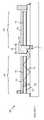
- FIG. 1is top view of a prior art LED.
- FIG. 2is a cross-sectional view of prior art LED 20 through line 2 - 2 shown in FIG. 1 .
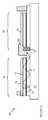
- FIG. 3is a top view of prior art light source.
- FIG. 4is a cross-sectional view of prior art light source 40 through line 4 - 4 shown in FIG. 3 .
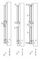
- FIG. 5is a top view of one embodiment of a light source according to the present invention.
- FIG. 6is a cross-sectional view of light source 60 through line 6 - 6 shown in FIG. 5 .
- FIG. 7is another cross-sectional view of light source 60 .
- FIG. 8illustrates an embodiment of the present invention in which the light loss problem is reduced by using a clear insulator to fill the bottom of the isolation trench.
- FIGS. 9A-9Dillustrate the manner in which a light source that utilizes a metal serial connection electrode is fabricated.
- FIGS. 10A-10Care cross-sectional views of a portion of a wafer having a light source in which the isolation trench is filled with glass.
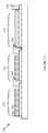
- FIG. 11is a cross-sectional view of a light source having three segments.
- FIG. 1is top view of LED 20
- FIG. 2is a cross-sectional view of LED 20 through line 2 - 2 shown in FIG. 1
- LED 20is constructed by growing a light emitting structure 21 having three layers on a sapphire substrate 19 .
- the first layer 22is an n-type GaN material.
- the second layer 23is an active layer that emits light when holes and electrons combine therein.
- the third layeris a p-type GaN layer 24 .
- Each of these layersmay include a number of sub-layers. Since the functions of these sub-layers are well known in the art and are not central to the present discussion, the details of these sub-layers have been omitted from the drawings and the following discussion.
- a trench 28is etched through layers 23 and 24 and a contact 26 is deposited on the bottom surface of the trench 28 to provide an electrical connection to layer 22 .
- the electrical connection to layer 24is provided by a transparent electrode 27 that is typically constructed from indium tin oxide (ITO).
- ITOindium tin oxide
- Layer 27is connected to a second contact 25 that provides the electrical connection to the power source. When power is provided to contacts 25 and 26 , light is generated in active layer 23 and extracted from LED 20 through transparent electrode 27 as shown at 29 .
- the resistivity of p-type GaNis much greater than that of the n-type GaN.
- the current density across active layer 23should be uniform. That is, the resistance of paths 31 - 33 should all be the same. In the absence of layer 27 , the resistance of path 31 would be much lower than that of path 33 , and hence, light generation would be concentrated in the active region around path 31 leading to a gradient in intensity across the surface of the LED.
- the resistivity of ITOis significantly less than that of the p-type GaN, the resistance through the ITO layer is not negligible.
- the power output of LEDsis increased, the losses in the ITO become significant and a gradient in light intensity results unless the ITO layer is increased in thickness. Unfortunately, as the ITO thickness increases, the amount of light absorbed in the ITO also increases. The light losses from absorption of light in the ITO become significant when the layer is increased to accommodate the current densities required in high power LEDs.
- FIGS. 3 and 4illustrate a prior art segmented light source.
- FIG. 3is a top view of light source 40
- FIG. 4is a cross-sectional view of light source 40 through line 4 - 4 shown in FIG. 3 .
- light source 40includes only two segments 51 and 52 ; however, it will be apparent that additional segments could be utilized.
- Light source 40is constructed by growing the conventional 3-layer structure 42 on a substrate 41 .
- An ITO layer 44is deposited over the p-layer. After the layers have been deposited, the structure is etched to expose layer 43 of the 3-layer structure.
- n-contact 46is then deposited in the etched trench to provide electrical contact to layer 43 .
- a p-contact 45is deposited on the segmented ITO layer. The n-contacts in each segment are connected together as shown at 47 . Similarly, the p-contacts in each segment are connected together as shown at 48 .
- this structurecan only be utilized in an arrangement in which the segments are connected in parallel, since the segments share a common n-type layer that remains connected after the trenches are etched.
- the current that must be carried by conductors 47 and 48is the sum of the currents needed to power the individual segments.
- Providing high currents at low voltagespresents problems that increase the cost of the light source or decreases the efficiency of light generation.
- the electrode metal thicknessmust be increased to lower the metallic resistance, which not only increases chip cost, since the metal is typically gold, but also introduces handling and mechanical issues.
- FIG. 5is a top view of light source 60
- FIG. 6is a cross-sectional view of light source 60 through line 6 - 6 shown in FIG. 5 .
- Light source 60includes two segments 64 and 65 ; however, it will be apparent from the following discussion that light sources having many more segments can be constructed from the teachings of the present invention.
- Light source 60is constructed from the same three-layer LED structure in which the layers are grown on a sapphire substrate 51 . The n-layer 52 is grown on substrate 51 , and then the active layer 55 and p-layer 53 are grown over n-layer 52 .
- Isolation trench 66includes a plateau 67 that extends only partially into layer 52 .
- the walls of isolation trench 66are covered by an insulating layer 57 that includes an open area 58 for making electrical contact to the portion of layer 52 associated with each segment.
- Insulating layer 57can be constructed from any material that provides an insulating layer that is free of pinhole defects. For example, SiNx can be used as the insulating material. Other materials can include polyimide, BCB, spin-on-glass and materials that are routinely used in the semiconductor industry for device planarization.
- a serial connection electrode 59is deposited in isolation trench 66 such that electrode 59 makes contact with layer 52 through opening 58 in insulating layer 57 . Electrode 59 also makes electrical contact with ITO layer 56 in the adjacent segment. Hence, when power is provided via electrodes 61 and 62 , segments 64 and 65 are connected in series. As a result, light source 60 operates at twice the voltage and half the current as light source 40 discussed above with respect to FIGS. 3 and 4 .
- insulating layer 57extends under electrodes 59 and 61 as shown at 57 a in FIG. 6 . Since electrode 59 is opaque, electrode 59 blocks light generated in the portion of active layer 55 immediately underlying electrode 59 .
- the thickness of the layers shown in the figuresis not to scale. In practice, the thickness of layer 53 is much smaller than that of layer 52 , and hence, electrode 59 blocks most of the light that is generated under electrode 59 . Accordingly, current that passes through layer 55 under electrode 59 is substantially wasted, since most of the light generated by that current is lost. The insulating layer extension blocks current from flowing through this wasted area of layer 55 , and hence, improves the overall efficiency of the light source. A similar issue is present under electrode 61 , and hence, the insulating layer is extended under that electrode as well.
- Serial connection electrode 59can be constructed by depositing a layer of metal such as copper or aluminum. However, such a layer prevents light from moving between segments 64 and 65 .
- a significant fraction of the light generated in active layer 55is trapped within the light source due to internal reflections at the boundaries of the light source such as the boundary between substrate 51 and layer 52 and the boundary between layer 53 and ITO layer 56 .
- An exemplary trapped rayis shown at 71 .
- the LEDincludes some mechanism that randomizes the angles of reflection at one or more of the reflecting surfaces.
- the upper surface of layer 53is roughened.
- the lightis either passed through the roughened surface or reflected back at a different angle with respect to the normal to the average surface of layer 53 .
- some of the light that is reflected at each reflectionleaves the surface at an angle that will allow that light to escape the next time the light is reflected upward and encounters surface 72 .
- electrode 59is a metal
- light ray 71will be intercepted by electrode 59 and will either be reflected back into segment 64 or be lost rather than proceeding into segment 65 and again reaching the portion of surface 72 in segment 65 . If the light is reflected back into segment 64 , some fraction of the light will escape on subsequent encounters with surface 71 .
- layers of metal deposited on etched surfacessuch as the surface of the isolation trench have a reflectivity that is significantly less than 100 percent. In this regard, it should be noted that the various layers in light source 60 are not drawn to scale. In practice, layer 52 is much thicker than the sum of layers 53 and 55 . Hence, a significant fraction of the light that strikes electrode 59 will be lost.
- this light loss problemis reduced by utilizing a transparent conductor such as ITO for electrode 59 .
- the transparency of electrode 59 for the purposes of propagating light between the segmentsis determined by the cross-section of the layer within the isolation trench that extends to substrate 51 , i.e., “t” shown in FIG. 7 .
- the resistance of electrode 59is determined by the entire cross-sectional area of electrode 59 , i.e., the dimension “T” shown in FIG. 7 .
- electrode 59can be made thick enough to have an acceptable light transmission while still providing a sufficiently low resistance to current flow between the segments.
- the portion of the insulating layer shown at 57 a in FIG. 6is not needed if electrode 59 is transparent, since light generated under electrode 59 can escape through electrode 59 .
- the use of a transparent electrode material for electrode 59also increases the usable area of segment 65 .
- FIG. 8illustrates an embodiment of the present invention in which the light loss problem discussed above is reduced by using a clear insulator to fill the bottom of the isolation trench.
- light source 80the portion of the isolation trench that extends to substrate 51 is filled with a clear insulator such as the glass layer shown at 81 .
- a separate metal electrode 82is used to make the serial connection between segments 84 and 85 .
- FIGS. 9A-9Dillustrate the manner in which a light source that utilizes a metal serial connection electrode is fabricated.
- FIGS. 9A-9Dare cross-sectional views of a portion of a wafer on which a light source 90 having two segments is shown at various stages in the fabrication process.
- light source 90is constructed by depositing GaN layers 52 , 55 , and 53 on a sapphire substrate 51 . This process is conventional in the art, and hence, will not be discussed in detail here. After the layers have been deposited, trenches 92 a - 92 c are etched through layers 53 and 55 and into layer the n-type layer 52 .
- trenches 92 a - 92 chave been etched, the wafer is masked and trenches 93 a - 93 c are etched down to substrate 51 .
- Trench 93 bis used to construct the isolation trench discussed above.
- a patterned insulating layer 94 of SiNis then deposited on the walls of the trenches, and openings 95 are etched in layer 94 to provide electrical access to layer 52 .
- a patterned ITO layer 96is deposited over the p-type layer 53 .
- the top surface of layer 53is etched to provide the desired scattering features before layer 96 is deposited.
- a patterned metal layeris then deposited to provide the serial connection electrode 97 and contacts 98 and 99 that are used to power light source 90 .
- serial connection electrode 97is constructed from ITO have advantages in terms of light extraction.
- the serial connection electrodeis constructed from ITO or a similar transparent conductor, the serial connection electrode is deposited at the same time as layer 96 .
- FIGS. 10A-10Care cross-sectional views of a portion of a wafer having a light source 100 in which the isolation trench is filled with glass.
- FIG. 10AThe fabrication process proceeds in the same manner as described above with respect to FIGS. 9A and 9B .
- the isolation trenchis filled with glass as shown at 101 .
- the glass layeris then partially etched to open a trench down to the plateau in layer 52 leaving a glass wall 102 as shown in FIG. 10B .
- a patterned layer 103 of SiNis then deposited as shown at 103 .
- An ITO layer 107is then deposited over the surface of layer 53 as shown at 107 in FIG. 10C and a patterned metal layer is deposited to form a serial connection electrode 104 and power contacts 105 and 106 .
- FIG. 11is a cross-sectional view of a light source having three segments.
- Light source 150utilizes segments 151 - 153 that are connected in series with the aid of series connection electrodes 162 and 163 .
- the light sourceis powered by applying a potential difference greater than or equal to 3 times the voltage needed to power each of the individual segments between contacts 161 and 164 .
- Light sources having even more segmentscan be constructed by duplicating segment 152 .
Landscapes
- Led Devices (AREA)
Abstract
Description
Claims (6)
Priority Applications (11)
| Application Number | Priority Date | Filing Date | Title |
|---|---|---|---|
| US12/208,502US7939839B2 (en) | 2008-09-11 | 2008-09-11 | Series connected segmented LED |
| KR1020117005709AKR101575922B1 (en) | 2008-09-11 | 2009-08-20 | Series connected segmented LED |
| CN200980132907.0ACN102132429B (en) | 2008-09-11 | 2009-08-20 | Series connected segmented led |
| JP2011526896AJP2012507134A (en) | 2008-09-11 | 2009-08-20 | Segmented LEDs connected in series |
| PCT/US2009/054456WO2010030482A2 (en) | 2008-09-11 | 2009-08-20 | Series connected segmented led |
| HK11113306.9AHK1158827B (en) | 2008-09-11 | 2009-08-20 | Series connected segmented led |
| EP09813430.7AEP2338183B1 (en) | 2008-09-11 | 2009-08-20 | Series connected segmented led |
| TW098129352ATWI462282B (en) | 2008-09-11 | 2009-09-01 | Semiconductor light source and method of manufacturing same |
| US13/049,492US8207543B2 (en) | 2008-09-11 | 2011-03-16 | Series connected segmented LED |
| JP2013145919AJP5586748B2 (en) | 2008-09-11 | 2013-07-11 | Light source and method of making the light source |
| US14/314,987USRE46155E1 (en) | 2008-09-11 | 2014-06-25 | Series connected segmented LED |
Applications Claiming Priority (1)
| Application Number | Priority Date | Filing Date | Title |
|---|---|---|---|
| US12/208,502US7939839B2 (en) | 2008-09-11 | 2008-09-11 | Series connected segmented LED |
Related Child Applications (1)
| Application Number | Title | Priority Date | Filing Date |
|---|---|---|---|
| US13/049,492ContinuationUS8207543B2 (en) | 2008-09-11 | 2011-03-16 | Series connected segmented LED |
Publications (2)
| Publication Number | Publication Date |
|---|---|
| US20100059768A1 US20100059768A1 (en) | 2010-03-11 |
| US7939839B2true US7939839B2 (en) | 2011-05-10 |
Family
ID=41798442
Family Applications (3)
| Application Number | Title | Priority Date | Filing Date |
|---|---|---|---|
| US12/208,502Active2029-06-12US7939839B2 (en) | 2008-09-11 | 2008-09-11 | Series connected segmented LED |
| US13/049,492CeasedUS8207543B2 (en) | 2008-09-11 | 2011-03-16 | Series connected segmented LED |
| US14/314,987ActiveUSRE46155E1 (en) | 2008-09-11 | 2014-06-25 | Series connected segmented LED |
Family Applications After (2)
| Application Number | Title | Priority Date | Filing Date |
|---|---|---|---|
| US13/049,492CeasedUS8207543B2 (en) | 2008-09-11 | 2011-03-16 | Series connected segmented LED |
| US14/314,987ActiveUSRE46155E1 (en) | 2008-09-11 | 2014-06-25 | Series connected segmented LED |
Country Status (7)
| Country | Link |
|---|---|
| US (3) | US7939839B2 (en) |
| EP (1) | EP2338183B1 (en) |
| JP (2) | JP2012507134A (en) |
| KR (1) | KR101575922B1 (en) |
| CN (1) | CN102132429B (en) |
| TW (1) | TWI462282B (en) |
| WO (1) | WO2010030482A2 (en) |
Cited By (8)
| Publication number | Priority date | Publication date | Assignee | Title |
|---|---|---|---|---|
| US20110121332A1 (en)* | 2009-11-23 | 2011-05-26 | Koninklijke Philips Electronics N.V. | Iii-v light emitting device with thin n-type region |
| US20110163347A1 (en)* | 2008-09-11 | 2011-07-07 | Ghulam Hasnain | Series Connected Segmented LED |
| US20110220942A1 (en)* | 2010-03-15 | 2011-09-15 | Choi Kwang Ki | Light emitting device and light emitting device package |
| US20120187431A1 (en)* | 2011-01-21 | 2012-07-26 | Michael John Bergmann | Light emitting diodes with low junction temperature and solid state backlight components including light emitting diodes with low junction temperature |
| US20120286317A1 (en)* | 2011-05-12 | 2012-11-15 | Jui Hung Yeh | Light-emitting element and the manufacturing method thereof |
| US8581267B2 (en) | 2011-11-09 | 2013-11-12 | Toshiba Techno Center Inc. | Series connected segmented LED |
| US9443903B2 (en) | 2006-06-30 | 2016-09-13 | Cree, Inc. | Low temperature high strength metal stack for die attachment |
| US10659164B2 (en) | 2016-06-23 | 2020-05-19 | Koninklijke Philips N.V. | Optical transmitter, optical receiver and optical link |
Families Citing this family (41)
| Publication number | Priority date | Publication date | Assignee | Title |
|---|---|---|---|---|
| US8368100B2 (en)* | 2007-11-14 | 2013-02-05 | Cree, Inc. | Semiconductor light emitting diodes having reflective structures and methods of fabricating same |
| TWI418060B (en)* | 2008-12-26 | 2013-12-01 | Lextar Electronics Corp | Method for manufacturing light-emitting diode wafer |
| US7982409B2 (en)* | 2009-02-26 | 2011-07-19 | Bridgelux, Inc. | Light sources utilizing segmented LEDs to compensate for manufacturing variations in the light output of individual segmented LEDs |
| US8084775B2 (en)* | 2010-03-16 | 2011-12-27 | Bridgelux, Inc. | Light sources with serially connected LED segments including current blocking diodes |
| TWI466325B (en)* | 2010-06-25 | 2014-12-21 | Toyoda Gosei Kk | Semiconductor light emitting element |
| US20120037946A1 (en)* | 2010-08-12 | 2012-02-16 | Chi Mei Lighting Technology Corporation | Light emitting devices |
| US10490598B2 (en) | 2010-09-13 | 2019-11-26 | Epistar Corporation | Light-emitting structure having a plurality of light-emitting structure units |
| KR101650518B1 (en)* | 2010-09-13 | 2016-08-23 | 에피스타 코포레이션 | Light-emitting structure |
| US9070851B2 (en) | 2010-09-24 | 2015-06-30 | Seoul Semiconductor Co., Ltd. | Wafer-level light emitting diode package and method of fabricating the same |
| US8536594B2 (en)* | 2011-01-28 | 2013-09-17 | Micron Technology, Inc. | Solid state lighting devices with reduced dimensions and methods of manufacturing |
| JP5541261B2 (en)* | 2011-03-23 | 2014-07-09 | 豊田合成株式会社 | Group III nitride semiconductor light emitting device |
| US9337366B2 (en) | 2011-07-26 | 2016-05-10 | Micron Technology, Inc. | Textured optoelectronic devices and associated methods of manufacture |
| US8937323B2 (en)* | 2011-09-02 | 2015-01-20 | Stanley Electric Co., Ltd. | LED array capable of reducing uneven brightness distribution |
| TW201347141A (en)* | 2012-05-04 | 2013-11-16 | Chi Mei Lighting Tech Corp | Light-emitting diode structure and manufacturing method thereof |
| CN103700682A (en)* | 2012-05-04 | 2014-04-02 | 奇力光电科技股份有限公司 | Light emitting diode structure and manufacturing method thereof |
| TW201407747A (en)* | 2012-08-03 | 2014-02-16 | Chi Mei Lighting Tech Corp | Light-emitting diode structure and manufacturing method thereof |
| US8816383B2 (en)* | 2012-07-06 | 2014-08-26 | Invensas Corporation | High performance light emitting diode with vias |
| US10804316B2 (en)* | 2012-08-07 | 2020-10-13 | Seoul Viosys Co., Ltd. | Wafer level light-emitting diode array |
| US10388690B2 (en) | 2012-08-07 | 2019-08-20 | Seoul Viosys Co., Ltd. | Wafer level light-emitting diode array |
| CN102983147A (en)* | 2012-09-24 | 2013-03-20 | 杭州士兰明芯科技有限公司 | Light emitting diode chip and production method thereof |
| KR101420789B1 (en)* | 2012-12-05 | 2014-07-18 | 주식회사 세미콘라이트 | Semiconductor light emitting device |
| KR101420788B1 (en)* | 2012-12-05 | 2014-07-18 | 주식회사 세미콘라이트 | Semiconductor light emitting device |
| KR20140073351A (en)* | 2012-12-06 | 2014-06-16 | 엘지이노텍 주식회사 | Light Emitting Device |
| US9093627B2 (en)* | 2012-12-21 | 2015-07-28 | Seoul Viosys Co., Ltd. | Light emitting diode and method of fabricating the same |
| US9356212B2 (en) | 2012-12-21 | 2016-05-31 | Seoul Viosys Co., Ltd. | Light emitting diode and method of fabricating the same |
| CN103915463B (en)* | 2013-01-09 | 2016-12-28 | 新世纪光电股份有限公司 | light emitting device |
| CN105074942A (en)* | 2013-02-25 | 2015-11-18 | 首尔伟傲世有限公司 | Light-emitting diode with multiple light-emitting elements and manufacturing method thereof |
| US10278243B2 (en) | 2014-03-06 | 2019-04-30 | Seoul Semiconductor Co., Ltd. | Backlight module with MJT LED and backlight unit including the same |
| KR102364160B1 (en)* | 2014-03-06 | 2022-02-21 | 서울반도체 주식회사 | Backlight module with mjt led and backlight unit having the same |
| US9444015B2 (en)* | 2014-06-18 | 2016-09-13 | X-Celeprint Limited | Micro assembled LED displays and lighting elements |
| US9343633B1 (en)* | 2014-10-31 | 2016-05-17 | Mikro Mesa Technology Co., Ltd. | Light-emitting diode lighting device |
| CN104409605B (en)* | 2014-11-28 | 2017-10-27 | 杭州士兰明芯科技有限公司 | A kind of high-voltage chip LED structure and preparation method thereof |
| USD826871S1 (en) | 2014-12-11 | 2018-08-28 | Cree, Inc. | Light emitting diode device |
| KR102326926B1 (en)* | 2014-12-26 | 2021-11-16 | 쑤저우 레킨 세미컨덕터 컴퍼니 리미티드 | Light emitting device, and lighting emitting device package |
| CN104733487B (en)* | 2015-03-20 | 2018-01-09 | 厦门乾照光电股份有限公司 | A kind of high-voltage LED with stereo luminous structure |
| JP2017059638A (en)* | 2015-09-15 | 2017-03-23 | 株式会社東芝 | Semiconductor light emitting device |
| CN205944139U (en) | 2016-03-30 | 2017-02-08 | 首尔伟傲世有限公司 | Ultraviolet ray light -emitting diode spare and contain this emitting diode module |
| KR102550005B1 (en)* | 2016-07-15 | 2023-07-03 | 서울바이오시스 주식회사 | Uv light emitting diode |
| TWI830759B (en)* | 2019-07-31 | 2024-02-01 | 晶元光電股份有限公司 | Led device and manufacturing method thereof |
| TWI886736B (en)* | 2019-07-31 | 2025-06-11 | 晶元光電股份有限公司 | Led device and manufacturing method thereof |
| TWI765788B (en)* | 2021-07-28 | 2022-05-21 | 友達光電股份有限公司 | Display panel and manufacturing method thereof |
Citations (11)
| Publication number | Priority date | Publication date | Assignee | Title |
|---|---|---|---|---|
| US4879250A (en) | 1988-09-29 | 1989-11-07 | The Boeing Company | Method of making a monolithic interleaved LED/PIN photodetector array |
| US6307218B1 (en) | 1998-11-20 | 2001-10-23 | Lumileds Lighting, U.S., Llc | Electrode structures for light emitting devices |
| US6410942B1 (en) | 1999-12-03 | 2002-06-25 | Cree Lighting Company | Enhanced light extraction through the use of micro-LED arrays |
| US6547249B2 (en) | 2001-03-29 | 2003-04-15 | Lumileds Lighting U.S., Llc | Monolithic series/parallel led arrays formed on highly resistive substrates |
| US6614056B1 (en) | 1999-12-01 | 2003-09-02 | Cree Lighting Company | Scalable led with improved current spreading structures |
| US6869812B1 (en) | 2003-05-13 | 2005-03-22 | Heng Liu | High power AllnGaN based multi-chip light emitting diode |
| US20070065962A1 (en)* | 2004-03-25 | 2007-03-22 | Nanosolar, Inc. | Manufacturing of optoelectronic devices |
| US20070102693A1 (en) | 2003-12-24 | 2007-05-10 | Hideo Nagai | Semiconductor light emitting device, lighting module, lighting apparatus, display element, and manufacturing method for semiconductor light emitting device |
| US20080230765A1 (en)* | 2007-03-19 | 2008-09-25 | Seoul Opto Device Co., Ltd. | Light emitting diode |
| US7560738B2 (en)* | 2003-07-04 | 2009-07-14 | Epistar Corporation | Light-emitting diode array having an adhesive layer |
| US7700960B2 (en)* | 2006-01-09 | 2010-04-20 | Seoul Opto Device Co., Ltd. | Light emitting diode with ITO layer and method for fabricating the same |
Family Cites Families (15)
| Publication number | Priority date | Publication date | Assignee | Title |
|---|---|---|---|---|
| JP3497741B2 (en) | 1998-09-25 | 2004-02-16 | 株式会社東芝 | Semiconductor light emitting device and method of driving semiconductor light emitting device |
| JP2002076437A (en)* | 2000-08-29 | 2002-03-15 | Kyocera Corp | LED array |
| US7880182B2 (en)* | 2002-07-15 | 2011-02-01 | Epistar Corporation | Light-emitting element array |
| TWI223460B (en)* | 2003-09-23 | 2004-11-01 | United Epitaxy Co Ltd | Light emitting diodes in series connection and method of making the same |
| JP2005136142A (en)* | 2003-10-30 | 2005-05-26 | Kyocera Corp | Light emitting diode array device and light emitting diode printer using the same |
| JP3904571B2 (en)* | 2004-09-02 | 2007-04-11 | ローム株式会社 | Semiconductor light emitting device |
| KR100721454B1 (en)* | 2005-11-10 | 2007-05-23 | 서울옵토디바이스주식회사 | Light emitting device for alternating current having photonic crystal structure and method for manufacturing same |
| JP5008911B2 (en)* | 2006-07-04 | 2012-08-22 | ローム株式会社 | Semiconductor light emitting device and manufacturing method thereof |
| JP2008060132A (en)* | 2006-08-29 | 2008-03-13 | Rohm Co Ltd | Semiconductor light emitting device and manufacturing method thereof |
| WO2008038910A1 (en)* | 2006-09-25 | 2008-04-03 | Seoul Opto Device Co., Ltd. | Light emitting diode having alingap active layer and method of fabricating the same |
| US7714348B2 (en)* | 2006-10-06 | 2010-05-11 | Ac-Led Lighting, L.L.C. | AC/DC light emitting diodes with integrated protection mechanism |
| TWI440210B (en)* | 2007-01-22 | 2014-06-01 | Cree Inc | Illumination device using external interconnection array of light-emitting device and manufacturing method thereof |
| CN101257071B (en)* | 2007-03-02 | 2011-09-07 | 普瑞光电股份有限公司 | LED element and method for making LED element |
| US7939839B2 (en)* | 2008-09-11 | 2011-05-10 | Bridgelux, Inc. | Series connected segmented LED |
| US7982409B2 (en)* | 2009-02-26 | 2011-07-19 | Bridgelux, Inc. | Light sources utilizing segmented LEDs to compensate for manufacturing variations in the light output of individual segmented LEDs |
- 2008
- 2008-09-11USUS12/208,502patent/US7939839B2/enactiveActive
- 2009
- 2009-08-20CNCN200980132907.0Apatent/CN102132429B/enactiveActive
- 2009-08-20EPEP09813430.7Apatent/EP2338183B1/enactiveActive
- 2009-08-20JPJP2011526896Apatent/JP2012507134A/enactivePending
- 2009-08-20KRKR1020117005709Apatent/KR101575922B1/enactiveActive
- 2009-08-20WOPCT/US2009/054456patent/WO2010030482A2/enactiveApplication Filing
- 2009-09-01TWTW098129352Apatent/TWI462282B/enactive
- 2011
- 2011-03-16USUS13/049,492patent/US8207543B2/ennot_activeCeased
- 2013
- 2013-07-11JPJP2013145919Apatent/JP5586748B2/enactiveActive
- 2014
- 2014-06-25USUS14/314,987patent/USRE46155E1/enactiveActive
Patent Citations (12)
| Publication number | Priority date | Publication date | Assignee | Title |
|---|---|---|---|---|
| US4879250A (en) | 1988-09-29 | 1989-11-07 | The Boeing Company | Method of making a monolithic interleaved LED/PIN photodetector array |
| US6307218B1 (en) | 1998-11-20 | 2001-10-23 | Lumileds Lighting, U.S., Llc | Electrode structures for light emitting devices |
| US6614056B1 (en) | 1999-12-01 | 2003-09-02 | Cree Lighting Company | Scalable led with improved current spreading structures |
| US6885036B2 (en) | 1999-12-01 | 2005-04-26 | Cree, Inc. | Scalable LED with improved current spreading structures |
| US6410942B1 (en) | 1999-12-03 | 2002-06-25 | Cree Lighting Company | Enhanced light extraction through the use of micro-LED arrays |
| US6547249B2 (en) | 2001-03-29 | 2003-04-15 | Lumileds Lighting U.S., Llc | Monolithic series/parallel led arrays formed on highly resistive substrates |
| US6869812B1 (en) | 2003-05-13 | 2005-03-22 | Heng Liu | High power AllnGaN based multi-chip light emitting diode |
| US7560738B2 (en)* | 2003-07-04 | 2009-07-14 | Epistar Corporation | Light-emitting diode array having an adhesive layer |
| US20070102693A1 (en) | 2003-12-24 | 2007-05-10 | Hideo Nagai | Semiconductor light emitting device, lighting module, lighting apparatus, display element, and manufacturing method for semiconductor light emitting device |
| US20070065962A1 (en)* | 2004-03-25 | 2007-03-22 | Nanosolar, Inc. | Manufacturing of optoelectronic devices |
| US7700960B2 (en)* | 2006-01-09 | 2010-04-20 | Seoul Opto Device Co., Ltd. | Light emitting diode with ITO layer and method for fabricating the same |
| US20080230765A1 (en)* | 2007-03-19 | 2008-09-25 | Seoul Opto Device Co., Ltd. | Light emitting diode |
Non-Patent Citations (1)
| Title |
|---|
| International Search Report and Written Opinion, PCT/US2009/054456, all pages, Apr. 7, 2010. |
Cited By (28)
| Publication number | Priority date | Publication date | Assignee | Title |
|---|---|---|---|---|
| US9443903B2 (en) | 2006-06-30 | 2016-09-13 | Cree, Inc. | Low temperature high strength metal stack for die attachment |
| US20110163347A1 (en)* | 2008-09-11 | 2011-07-07 | Ghulam Hasnain | Series Connected Segmented LED |
| US8207543B2 (en)* | 2008-09-11 | 2012-06-26 | Bridgelux, Inc. | Series connected segmented LED |
| USRE46155E1 (en)* | 2008-09-11 | 2016-09-20 | Kabushiki Kaisha Toshiba | Series connected segmented LED |
| US8581229B2 (en)* | 2009-11-23 | 2013-11-12 | Koninklijke Philips N.V. | III-V light emitting device with thin n-type region |
| US20110121332A1 (en)* | 2009-11-23 | 2011-05-26 | Koninklijke Philips Electronics N.V. | Iii-v light emitting device with thin n-type region |
| US8878160B2 (en) | 2009-11-23 | 2014-11-04 | Koninklijke Philips N.V. | III-V light emitting device with thin n-type region |
| US9837581B2 (en) | 2010-03-15 | 2017-12-05 | Lg Innotek Co., Ltd. | Light emitting device and light emitting device package |
| US9577150B2 (en)* | 2010-03-15 | 2017-02-21 | Lg Innotek Co., Ltd. | Light emitting device and light emitting device package |
| US10833226B2 (en) | 2010-03-15 | 2020-11-10 | Lg Innotek Co., Ltd. | Light emitting device and light emitting device package |
| US8791494B2 (en) | 2010-03-15 | 2014-07-29 | Lg Innotek Co., Ltd. | Light emitting device and light emitting device package |
| US8847268B2 (en)* | 2010-03-15 | 2014-09-30 | Lg Innotek Co., Ltd. | Light emitting device and light emitting device package |
| US10510929B2 (en) | 2010-03-15 | 2019-12-17 | Lg Innotek Co., Ltd. | Light emitting device and light emitting device package |
| US9076930B2 (en) | 2010-03-15 | 2015-07-07 | Lg Innotek Co., Ltd. | Light emitting device and light emitting device package |
| US10084116B2 (en)* | 2010-03-15 | 2018-09-25 | Lg Innotek Co., Ltd. | Light emitting device and light emitting device package |
| US9287457B2 (en) | 2010-03-15 | 2016-03-15 | Lg Innotek Co., Ltd. | Light emitting device and light emitting device package |
| US20180062045A1 (en)* | 2010-03-15 | 2018-03-01 | Lg Innotek Co., Ltd. | Light emitting device and light emitting device package |
| US20110220942A1 (en)* | 2010-03-15 | 2011-09-15 | Choi Kwang Ki | Light emitting device and light emitting device package |
| US8698184B2 (en)* | 2011-01-21 | 2014-04-15 | Cree, Inc. | Light emitting diodes with low junction temperature and solid state backlight components including light emitting diodes with low junction temperature |
| US20120187431A1 (en)* | 2011-01-21 | 2012-07-26 | Michael John Bergmann | Light emitting diodes with low junction temperature and solid state backlight components including light emitting diodes with low junction temperature |
| US8344392B2 (en)* | 2011-05-12 | 2013-01-01 | Epistar Corporation | Light-emitting element and the manufacturing method thereof |
| US20120286317A1 (en)* | 2011-05-12 | 2012-11-15 | Jui Hung Yeh | Light-emitting element and the manufacturing method thereof |
| US8754439B2 (en) | 2011-05-12 | 2014-06-17 | Epistar Corporation | Light-emitting element and the manufacturing method thereof |
| US9391234B2 (en) | 2011-11-09 | 2016-07-12 | Toshiba Corporation | Series connected segmented LED |
| US9123853B2 (en) | 2011-11-09 | 2015-09-01 | Manutius Ip, Inc. | Series connected segmented LED |
| US8581267B2 (en) | 2011-11-09 | 2013-11-12 | Toshiba Techno Center Inc. | Series connected segmented LED |
| US10659164B2 (en) | 2016-06-23 | 2020-05-19 | Koninklijke Philips N.V. | Optical transmitter, optical receiver and optical link |
| US10790907B2 (en) | 2016-06-23 | 2020-09-29 | Koninklijke Philips N.V. | Optical transmitter, optical receiver and optical link |
Also Published As
| Publication number | Publication date |
|---|---|
| JP2013232677A (en) | 2013-11-14 |
| US20110163347A1 (en) | 2011-07-07 |
| CN102132429A (en) | 2011-07-20 |
| WO2010030482A2 (en) | 2010-03-18 |
| KR20110057152A (en) | 2011-05-31 |
| EP2338183A4 (en) | 2013-03-27 |
| US20100059768A1 (en) | 2010-03-11 |
| TWI462282B (en) | 2014-11-21 |
| JP2012507134A (en) | 2012-03-22 |
| EP2338183A2 (en) | 2011-06-29 |
| EP2338183B1 (en) | 2018-01-10 |
| US8207543B2 (en) | 2012-06-26 |
| CN102132429B (en) | 2015-08-26 |
| USRE46155E1 (en) | 2016-09-20 |
| WO2010030482A3 (en) | 2010-05-27 |
| JP5586748B2 (en) | 2014-09-10 |
| TW201027798A (en) | 2010-07-16 |
| KR101575922B1 (en) | 2015-12-08 |
| HK1158827A1 (en) | 2012-07-20 |
Similar Documents
| Publication | Publication Date | Title |
|---|---|---|
| US7939839B2 (en) | Series connected segmented LED | |
| US8026527B2 (en) | LED structure | |
| TWI515919B (en) | Improved multi-contact LED | |
| US20220028921A1 (en) | Wafer level light-emitting diode array | |
| CN102201426B (en) | Light-emitting Diode And Its Making Method | |
| US9123853B2 (en) | Series connected segmented LED | |
| JP2018529230A (en) | Light emitting device and light emitting device package including the same | |
| CN103178185B (en) | Light emitting device | |
| TWI575783B (en) | Photoelectric semiconductor wafer and method of manufacturing optoelectronic semiconductor wafer | |
| US12188974B2 (en) | Method for testing light-emitting devices | |
| HK1158827B (en) | Series connected segmented led | |
| TW200834972A (en) | Light-emitting diode chip with large illumination area |
Legal Events
| Date | Code | Title | Description |
|---|---|---|---|
| AS | Assignment | Owner name:BRIDGELUX, INC.,CALIFORNIA Free format text:ASSIGNMENT OF ASSIGNORS INTEREST;ASSIGNOR:HASNAIN, GHULAM, MR.;REEL/FRAME:021517/0592 Effective date:20080911 Owner name:BRIDGELUX, INC., CALIFORNIA Free format text:ASSIGNMENT OF ASSIGNORS INTEREST;ASSIGNOR:HASNAIN, GHULAM, MR.;REEL/FRAME:021517/0592 Effective date:20080911 | |
| STCF | Information on status: patent grant | Free format text:PATENTED CASE | |
| AS | Assignment | Owner name:WHITE OAK GLOBAL ADVISORS, LLC, AS COLLATERAL AGEN Free format text:SECURITY AGREEMENT;ASSIGNOR:BRIDGELUX, INC.;REEL/FRAME:029281/0844 Effective date:20121109 | |
| AS | Assignment | Owner name:BRIDGELUX, INC., CALIFORNIA Free format text:RELEASE BY SECURED PARTY;ASSIGNOR:WHITE OAK GLOBAL ADVISORS, LLC, AS COLLATERAL AGENT;REEL/FRAME:030466/0093 Effective date:20130516 | |
| AS | Assignment | Owner name:TOSHIBA TECHNO CENTER INC., JAPAN Free format text:ASSIGNMENT OF ASSIGNORS INTEREST;ASSIGNOR:BRIDGELUX, INC.;REEL/FRAME:030724/0395 Effective date:20130516 | |
| AS | Assignment | Owner name:KABUSHIKI KAISHA TOSHIBA, JAPAN Free format text:ASSIGNMENT OF ASSIGNORS INTEREST;ASSIGNOR:TOSHIBA TECHNO CENTER INC.;REEL/FRAME:033169/0625 Effective date:20140516 | |
| FPAY | Fee payment | Year of fee payment:4 | |
| AS | Assignment | Owner name:TOSHIBA ELECTRONIC DEVICES & STORAGE CORPORATION, Free format text:ASSIGNMENT OF ASSIGNORS INTEREST;ASSIGNOR:KABUSHIKI KAISHA TOSHIBA;REEL/FRAME:046364/0164 Effective date:20180611 | |
| AS | Assignment | Owner name:SAMSUNG ELECTRONICS CO., LTD., KOREA, REPUBLIC OF Free format text:ASSIGNMENT OF ASSIGNORS INTEREST;ASSIGNOR:TOSHIBA ELECTRONIC DEVICES & STORAGE CORPORATION;REEL/FRAME:046986/0159 Effective date:20180720 | |
| MAFP | Maintenance fee payment | Free format text:PAYMENT OF MAINTENANCE FEE, 8TH YEAR, LARGE ENTITY (ORIGINAL EVENT CODE: M1552); ENTITY STATUS OF PATENT OWNER: LARGE ENTITY Year of fee payment:8 | |
| MAFP | Maintenance fee payment | Free format text:PAYMENT OF MAINTENANCE FEE, 12TH YEAR, LARGE ENTITY (ORIGINAL EVENT CODE: M1553); ENTITY STATUS OF PATENT OWNER: LARGE ENTITY Year of fee payment:12 |