US7936625B2 - Pipeline sensing using voltage storage elements to read non-volatile memory cells - Google Patents
Pipeline sensing using voltage storage elements to read non-volatile memory cellsDownload PDFInfo
- Publication number
- US7936625B2 US7936625B2US12/409,671US40967109AUS7936625B2US 7936625 B2US7936625 B2US 7936625B2US 40967109 AUS40967109 AUS 40967109AUS 7936625 B2US7936625 B2US 7936625B2
- Authority
- US
- United States
- Prior art keywords
- read
- memory cells
- memory
- voltage
- vse
- Prior art date
- Legal status (The legal status is an assumption and is not a legal conclusion. Google has not performed a legal analysis and makes no representation as to the accuracy of the status listed.)
- Expired - Fee Related, expires
Links
Images


Classifications
- G—PHYSICS
- G11—INFORMATION STORAGE
- G11C—STATIC STORES
- G11C7/00—Arrangements for writing information into, or reading information out from, a digital store
- G11C7/10—Input/output [I/O] data interface arrangements, e.g. I/O data control circuits, I/O data buffers
- G11C7/1015—Read-write modes for single port memories, i.e. having either a random port or a serial port
- G11C7/1039—Read-write modes for single port memories, i.e. having either a random port or a serial port using pipelining techniques, i.e. using latches between functional memory parts, e.g. row/column decoders, I/O buffers, sense amplifiers
- G—PHYSICS
- G11—INFORMATION STORAGE
- G11C—STATIC STORES
- G11C11/00—Digital stores characterised by the use of particular electric or magnetic storage elements; Storage elements therefor
- G11C11/02—Digital stores characterised by the use of particular electric or magnetic storage elements; Storage elements therefor using magnetic elements
- G11C11/16—Digital stores characterised by the use of particular electric or magnetic storage elements; Storage elements therefor using magnetic elements using elements in which the storage effect is based on magnetic spin effect
- G11C11/165—Auxiliary circuits
- G11C11/1673—Reading or sensing circuits or methods
- G—PHYSICS
- G11—INFORMATION STORAGE
- G11C—STATIC STORES
- G11C11/00—Digital stores characterised by the use of particular electric or magnetic storage elements; Storage elements therefor
- G11C11/02—Digital stores characterised by the use of particular electric or magnetic storage elements; Storage elements therefor using magnetic elements
- G11C11/16—Digital stores characterised by the use of particular electric or magnetic storage elements; Storage elements therefor using magnetic elements using elements in which the storage effect is based on magnetic spin effect
- G11C11/165—Auxiliary circuits
- G11C11/1675—Writing or programming circuits or methods
- G—PHYSICS
- G11—INFORMATION STORAGE
- G11C—STATIC STORES
- G11C11/00—Digital stores characterised by the use of particular electric or magnetic storage elements; Storage elements therefor
- G11C11/02—Digital stores characterised by the use of particular electric or magnetic storage elements; Storage elements therefor using magnetic elements
- G11C11/16—Digital stores characterised by the use of particular electric or magnetic storage elements; Storage elements therefor using magnetic elements using elements in which the storage effect is based on magnetic spin effect
- G11C11/165—Auxiliary circuits
- G11C11/1693—Timing circuits or methods
- G—PHYSICS
- G11—INFORMATION STORAGE
- G11C—STATIC STORES
- G11C11/00—Digital stores characterised by the use of particular electric or magnetic storage elements; Storage elements therefor
- G11C11/56—Digital stores characterised by the use of particular electric or magnetic storage elements; Storage elements therefor using storage elements with more than two stable states represented by steps, e.g. of voltage, current, phase, frequency
- G11C11/5607—Digital stores characterised by the use of particular electric or magnetic storage elements; Storage elements therefor using storage elements with more than two stable states represented by steps, e.g. of voltage, current, phase, frequency using magnetic storage elements
- G—PHYSICS
- G11—INFORMATION STORAGE
- G11C—STATIC STORES
- G11C13/00—Digital stores characterised by the use of storage elements not covered by groups G11C11/00, G11C23/00, or G11C25/00
- G—PHYSICS
- G11—INFORMATION STORAGE
- G11C—STATIC STORES
- G11C13/00—Digital stores characterised by the use of storage elements not covered by groups G11C11/00, G11C23/00, or G11C25/00
- G11C13/0002—Digital stores characterised by the use of storage elements not covered by groups G11C11/00, G11C23/00, or G11C25/00 using resistive RAM [RRAM] elements
- G11C13/0021—Auxiliary circuits
- G11C13/004—Reading or sensing circuits or methods
- G—PHYSICS
- G11—INFORMATION STORAGE
- G11C—STATIC STORES
- G11C13/00—Digital stores characterised by the use of storage elements not covered by groups G11C11/00, G11C23/00, or G11C25/00
- G11C13/0002—Digital stores characterised by the use of storage elements not covered by groups G11C11/00, G11C23/00, or G11C25/00 using resistive RAM [RRAM] elements
- G11C13/0021—Auxiliary circuits
- G11C13/0061—Timing circuits or methods
- G—PHYSICS
- G11—INFORMATION STORAGE
- G11C—STATIC STORES
- G11C7/00—Arrangements for writing information into, or reading information out from, a digital store
- G11C7/06—Sense amplifiers; Associated circuits, e.g. timing or triggering circuits
- G11C7/08—Control thereof
- G—PHYSICS
- G11—INFORMATION STORAGE
- G11C—STATIC STORES
- G11C13/00—Digital stores characterised by the use of storage elements not covered by groups G11C11/00, G11C23/00, or G11C25/00
- G11C13/0002—Digital stores characterised by the use of storage elements not covered by groups G11C11/00, G11C23/00, or G11C25/00 using resistive RAM [RRAM] elements
- G11C13/0021—Auxiliary circuits
- G11C13/004—Reading or sensing circuits or methods
- G11C2013/0054—Read is performed on a reference element, e.g. cell, and the reference sensed value is used to compare the sensed value of the selected cell
Definitions
- Data storage devicesgenerally operate to store and retrieve data in a fast and efficient manner.
- Some storage devicesutilize a semiconductor array of solid-state memory cells to store individual bits of data.
- Such memory cellscan be volatile or non-volatile.
- volatile memory cellsgenerally retain data stored in memory only so long as operational power continues to be supplied to the device.
- Non-volatile memory cellsgenerally retain data stored in memory even in the absence of the application of operational power.
- Non-volatile memory cellscan take a variety of constructions, such as spin-torque transfer random access memory (STRAM), resistive RAM (RRAM), flash, etc.
- STRAMspin-torque transfer random access memory
- RRAMresistive RAM
- flashetc.
- the cellscan be configured to have different electrical resistances to store different logical states.
- the resistance of the cellscan be subsequently detected during a read operation by applying a read current and sensing a voltage drop across the cell. While it is generally desirable to carry out read operations quickly, various effects can reduce the overall rate at which data can be read from an array. These effects can include parasitic capacitances associated with the charging of access lines, and overhead time required to configure the cells for a read operation.
- Various embodiments of the present inventionare generally directed to a method and apparatus for carrying out a pipeline sensing operation to read data from a semiconductor memory array.
- a methodgenerally comprises storing a read voltage from a first memory cell in a voltage storage element (VSE); comparing the read voltage to a reference voltage to identify a corresponding memory state of the first memory cell; and storing a second read voltage from a second memory cell in a second VSE during the comparing step to carry out a pipeline sensing operation upon the first and second memory cells.
- VSEvoltage storage element
- an apparatusgenerally comprises a memory array of semiconductor memory cells, and a control circuit which carries out a pipeline sense operation to read data from the array by simultaneously applying bias currents to a first set of memory cells from the array while storing read voltages generated thereby in a corresponding first set of voltage storage elements (VSEs), and then sequentially comparing the read voltages stored in said first set of VSEs with at least one reference value to serially output a logical sequence corresponding to the memory states of the first set of memory cells.
- VSEsvoltage storage elements
- an apparatusgenerally comprises a memory array of semiconductor memory cells, and first means for carrying out a pipeline sense operation to read data from the array.
- FIG. 1is a generalized functional representation of an exemplary data storage device constructed and operated in accordance with various embodiments of the present invention.
- FIG. 2generally illustrates a manner in which data are written to a memory cell of the memory array of FIG. 1 .
- FIG. 3generally illustrates a manner in which data are read from the memory cell of FIG. 2 .
- FIGS. 4A-4Bshow exemplary constructions of a magnetic tunneling junction (MTJ) of a spin-torque transfer random access memory (STRAM) memory cell.
- MTJmagnetic tunneling junction
- STRAMspin-torque transfer random access memory
- FIGS. 5A-5Bshow exemplary constructions of a resistive random access memory (RRAM) memory cell.
- RRAMresistive random access memory
- FIG. 6sets forth a schematic representation of a manner in which data are read from the memory array in accordance with various embodiments of the present invention in which an external reference is used.
- FIG. 7provides an associated timing diagram to generally illustrate a sequence of FIG. 6 .
- FIG. 8provides a schematic representation of another manner in which data are read from the memory array in accordance with various embodiments in which a dummy reference is used.
- FIG. 9provides an associated timing diagram to generally illustrate a sequence of FIG. 8 .
- FIG. 10provides a schematic representation of yet another manner in which data are read from the memory array in accordance with various embodiments in which a self-reference is used.
- FIG. 11provides an associated timing diagram to generally illustrate a sequence of FIG. 10 .
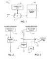
- FIG. 1provides a functional block representation of a data storage device 100 to illustrate an exemplary environment in which various embodiments of the present invention can be advantageously practiced.
- the device 100includes a top level controller 102 , an interface (I/F) circuit 104 and a non-volatile data storage array 106 .
- the I/F circuit 104operates under the direction of the controller 102 to transfer user data between the array 106 and a host device (not shown).
- the deviceis characterized as a solid-state drive (SSD)
- the controller 102is a programmable microcontroller
- the array 106comprises an array of nonvolatile memory cells (unit cells), one of which is represented in FIG. 2 at 110 .
- Dataare written to the memory cells 110 using a write power source 112 to apply a suitable write input such as in the form of a write voltage and/or current to configure the memory cell 110 to a desired programmed state.
- the programmed statecan be subsequently read from the memory cell 110 as shown in FIG. 3 .
- a read currentis supplied from a suitable read current source 114 .
- a voltage drop across the memory cell V MCis sensed by a sense amplifier 116 , and compared to a reference voltage V REF from a voltage reference source 118 .
- the output state of the sense amplifier 116will nominally reflect the programmed state of the memory cell (e.g., a logical 0, a logical 1, a logical “10,” etc.).
- the memory cells 110take a spin-torque transfer random access memory (STRAM) configuration, as generally shown in FIGS. 4A-4B .
- STRAMspin-torque transfer random access memory
- a resistive sense element (RSE) 120 characterized as a magnetic tunneling junction (MTJ)includes a fixed magnetic reference layer 122 and a free magnetic layer 124 separated by an intervening barrier layer 126 .
- the reference layer 122comprises spin polarizing material that orients the spin of current passing through the MTJ 120 in a predetermined direction.
- the magnetization direction of the reference layer 122may be pinned to a separate layer (not shown) that maintains the reference layer in a specified magnetic orientation.
- the free layer 124is formed of a suitable magnetic material arranged to have selectively different magnetization directions which are established responsive to the application of different write currents.
- the intervening barrier layer 126can take any number of constructions, such as Magnesium Oxide (MgO). While the respective magnetization directions are shown to be substantially perpendicular to the direction of write current, other magnetic orientations, including in-line orientations, can be utilized as desired. Additional layers, including seed layers, shield layers, and secondary free and/or reference layers can be incorporated into the MTJ as desired.
- a low resistance state for the MTJ 120is achieved when the magnetization of the free layer 124 is oriented to be substantially in the same direction (parallel) as the magnetization of the reference layer 122 . This orientation is shown in FIG. 4A .
- a write currentpasses through the MTJ 120 so that the magnetization direction of the reference layer 122 sets the magnetic orientation of the free layer 124 . Since electrons flow in the direction opposite to the direction of current, the write current direction passes from the free layer 124 to the reference layer 122 , so that the electrons travel from the reference layer 122 to the free layer 124 .
- a high resistance state for the MTJ 120is shown in FIG. 4B and is characterized as an anti-parallel orientation in which the magnetization direction of the free layer 124 is substantially opposite that of the reference layer 122 .
- a write currentpasses through the MTJ 120 from the reference layer 122 to the free layer 124 so that spin-polarized electrons flow into the free layer 124 .
- a different logical stateis assigned to each of the programmable resistances of the MTJ.
- the low resistance, parallel (P) state of FIG. 4Ais used to represent a logical 1
- the high resistance, anti-parallel (AP) state of FIG. 4Bis used to represent a logical 1.
- Additional programmed statescan be used when the MTJ is configured to store multiple bits. For example, programmed resistances R 1 ⁇ R 2 ⁇ R 3 ⁇ R 4 can be used to respectively store multi-bit values “00,” “01,” “10” and “11.”
- FIGS. 5A and 5Bshow an alternative construction for the memory cell 110 of FIGS. 2-3 characterized as a resistive random access memory (RRAM) cell.
- An RRAM resistive sense element (RSE) 130includes opposing metal or metal alloy electrode layers 132 , 134 which are separated by an intervening oxide layer 136 .
- a first, higher resistance programmed stateis denoted by FIG. 5A
- a second, lower resistance programmed stateis denoted by FIG. 5B .
- the relatively higher resistance stateis established by the nominal electrical resistance of the oxide layer 136 .
- Application of a suitable write voltage potential and/or write current in a selected direction across the RSE 130will induce metal migration from the electrode layer 132 , forming one or more electrically conductive metallization filaments 138 through the oxide layer as shown in FIG. 5B .
- Such filamentsgenerally operate to lower the characteristic resistance of the cell.
- an appropriate write voltage potential and/or currentis applied through the RSE 130 in the opposite direction.
- stepsmay include: the pre-charging of the associated bit line to an initial pre-determined voltage level, the charging of the bit line by read current (in a current mode) or a voltage driver (in a voltage mode), the enabling of the sense amplifier, the actual sensing and comparison by the amplifier to output the memory state, and the latching of the output memory state in a buffer or other location. If self-reference is used, additional time may be required to generate and store the appropriate V REF for use by the sense amplifier.
- the charging time for the bit linecan be relatively long due to parasitic capacitances and other effects, particularly when the size of the memory block being accessed is relatively large.
- the use of self-reference schemescan also increase the time required to carry out a read operation due to the timing overhead required to configure the circuit (extra read/write operations, etc.).
- various embodiments of the present inventionare generally directed to the implementation of a pipeline sensing scheme to improve the read throughput performance of a memory array.
- This schemegenerally reduces the delays associated with the reading of data, including the bit line charging delays and self-reference overhead operations discussed above.
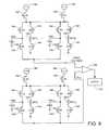
- FIG. 6shows a schematic representation of a portion of the memory device array of FIG. 1 in accordance with some embodiments.
- FIG. 6utilizes STRAM memory cells with MTJs 120 as set forth in FIGS. 4A-4B , although other configurations of memory cells could be alternatively used.
- FIG. 6represents circuitry for N memory cells (MTJ 1 to MTJ N ).
- VSEs 140Voltage storage elements 140 are coupled to the bit lines of the MTJs 120 .
- the VSEs 140are characterized as capacitors in FIG. 6 , although other constructions can alternatively be used.
- One VSE 140can be provisioned for each MTJ 120 , or multiple MTJs 120 can selectively utilize a common VSE 140 in turn to save space.
- Other elements in FIG. 6include respective current sources 142 , switches S 1 -S 5 (transistors) 144 , comparator (sense amplifier) 146 , an external V REF current source 148 , and output latch 150 .
- multiple ones of the MTJs 120are accessed simultaneously through the application of read current by the sources 142 thereto via associated bit lines (BL).
- the corresponding read voltages from the MTJse.g., the voltage drops from bit lines BL to source lines SL
- the read current from the respective sources 142is thereafter removed from the bit lines, and the sense amplifier 146 is sequentially enabled to sense the voltage of each of the VSEs 140 serially in turn.
- the circuitry of FIG. 6repeats the foregoing operation on a next set of memory cells.
- the circuitrygenerally operates to read a first memory cell to obtain a first read voltage indicative of a memory state of the first cell, to store the first read voltage in a first voltage storage element (VSE), and to sense the read voltage in the first VSE to identify said memory state while a second memory cell is read and a second read voltage therefor is stored in a second VSE for subsequent sensing thereof to carry out a pipeline reading of said memory cells.
- VSEvoltage storage element
- multiple cellsare simultaneously read and read voltages therefor are simultaneously stored, after which the read voltages are sequentially sensed.
- FIG. 7shows a generalized timing representation for the operation of FIG. 6 in accordance with some embodiments.
- a first bit line charging and VSE storage block 152represents the time required to store associated read voltages in VSEs for a first set of memory cells.
- a second bit line charging block 154corresponds to the same operations being carried out for a second set of memory cells. It is noted that both blocks 152 and 154 are carried out at the same time, and each of the sets of memory cells can be any number of cells, including just a single cell or a relatively large number of cells (including an entire sector or more).
- a first sensing operationthereafter takes place at block 156 for the first set of memory cells, and a second sensing operation takes place at block 158 for the second set of memory cells. It will be noted that the sensing operation at block 158 immediately follows that of block 156 .
- a third set of memory cellsare shown to be accessed at block 160 and a fourth set of memory cells are being concurrently accessed at block 162 .
- the operations of blocks 160 , 162are nominally the same as carried out by blocks 152 , 154 . Sequential sensing operations are then carried out as shown at 164 , 166 .
- the substantially upper limit on how quickly data can be output from the arraywill generally be determined in relation to how quickly the sense amplifier can be enabled and operated, since the scheme attempts to obtain constant operation of the sense amplifier without delays or intervening latencies.
- This constant operation of the sense amplifieris represented in FIG. 7 by the serial cascade of sense blocks 156 , 158 , 164 , 166 . It will be appreciated that the process of FIG. 7 continues until all desired blocks have been read.
- the numbers of cells concurrently accessed during each of the access blocks 152 , 154 , 160 , 162can be selected in relation to the operational speed characteristics of the sense amplifier, and the time required to place such cells into a state whereby the read voltages can be stored by the VSEs. Different modes can be selectively enacted as desired for different environmental conditions (such as low power mode, high performance mode, etc.).
- the present schemecan provide significant power savings while maintaining exceptionally fast read operations without the need to incorporate costly features into the array to reduce the bit line charging time (such as through the use of amplifiers, current mirroring, etc.) as in the prior art.
- a single sense amplifier 146is shown in FIG. 6 , it will be appreciated that in alternative embodiments, multiple sense amplifiers can be configured in parallel to simultaneously operate to respectively output serialized voltage states to further increase read rate performance.
- FIG. 8provides an alternative schematic diagram representation of various embodiments of the present invention.
- FIG. 8is generally similar to FIG. 6 , and like reference numerals have been utilized to identify similar components.
- FIG. 8uses a dummy reference scheme wherein a number of dummy memory cells are supplied to generate the appropriate V REF .
- some proportion of the dummy cellsstore a first value (such as corresponding to a logical 1) and the remaining dummy cells store a second value (such as corresponding to a logical 0).
- an intermediary voltage level therebetweencan be readily generated. This intermediary voltage level can be used as the V REF value to differentiate between the stored states of the data cells.
- FIG. 8provides N data cells (MTJ 1 to MJT N ) to store data and M dummy cells (MTJ 1 ′ to MTJ M ′) to store dummy values used to generate V REF or other suitable values.
- Ncan be equal to M, or N can be greater or less than M, as desired.
- VSEs 140are coupled to the respective MTJs 120 to store read voltages therefrom. Both the read voltage and the V REF are stored in respective VSEs 140 for each sense operation.
- a corresponding timing diagramis set forth by FIG. 9 .
- Bit line charging and VSE storage operationstake place simultaneously for sets of data cells and dummy cells in blocks 172 , 174 , 176 and 178 , respectively.
- Sensing operationstake place serially at blocks 180 and 182 to sequentially output the data in relation to the sensed read voltages and reference voltages stored during blocks 172 , 174 , 176 and 178 .
- a next set of data cell and dummy cell bitline charging operationstake place at blocks 184 , 186 , 188 and 190 during the sensing operations of blocks 180 , 182 , and a next set of sensing operations occur at blocks 192 , 194 .
- the sequential sensing of the datatakes place substantially continuously without delay, latency or interruption, as shown by cascaded sensing blocks 180 , 182 , 192 and 194 .
- FIG. 10provides yet another alternative embodiment in which a self-reference scheme is employed.
- two VSEs 140are utilized for each MTJ 120 , one storing a read voltage and the other storing a reference voltage (V REF ).
- V REFreference voltage
- the circuitryotherwise generally operates in a manner similar to that set forth above for FIGS. 6 and 8 .
- a corresponding timing diagram for the circuitry of FIG. 10is shown in FIG. 11 .
- the steps carried out for a given MTJ 120are set forth by each row. These steps include a bit line charging block 200 , a latency delay at block 202 while a first one of the VSEs 140 is being charged to store the read voltage from the MTJ, and a sense operation 204 during which the value from the VSE is read.
- a write “0” operationis next carried out at block 206 , followed by a second bit line charging block 200 ′, a second latency delay 202 ′, and a second sense operation 204 ′.
- a restore operation 210then returns the MTJ to its original value. This sequence of steps is carried out simultaneously for a number of cells, as shown.
- This self-referencemaintains a certain amount of processing overhead in that the operation involves various read/write operations, and latency delays while the VSEs 140 are charged. Nevertheless, it will be noted from FIG. 11 that the sensing operations are controlled so as to be carried out in continuously sequential fashion, as indicated by the diagonal arrangement of the second sense operations 204 ′.
- the featured “first means”will be understood consistent with the foregoing discussion to correspond at least to the structure of FIGS. 1 , 6 , 8 and 10 .
- the circuitry in these figuresgenerally operates to carry out a pipeline sense operation to read data from the array by simultaneously applying bias currents to a first set of memory cells from the array while storing read voltages generated thereby in a corresponding first set of VSEs, and then sequentially comparing the read voltages stored in said first set of VSEs with at least one reference value to serially output a logical sequence corresponding to the memory states of the first set of memory cells.
Landscapes
- Engineering & Computer Science (AREA)
- Computer Hardware Design (AREA)
- Mram Or Spin Memory Techniques (AREA)
Abstract
Description
Claims (20)
Priority Applications (1)
| Application Number | Priority Date | Filing Date | Title |
|---|---|---|---|
| US12/409,671US7936625B2 (en) | 2009-03-24 | 2009-03-24 | Pipeline sensing using voltage storage elements to read non-volatile memory cells |
Applications Claiming Priority (1)
| Application Number | Priority Date | Filing Date | Title |
|---|---|---|---|
| US12/409,671US7936625B2 (en) | 2009-03-24 | 2009-03-24 | Pipeline sensing using voltage storage elements to read non-volatile memory cells |
Publications (2)
| Publication Number | Publication Date |
|---|---|
| US20100246250A1 US20100246250A1 (en) | 2010-09-30 |
| US7936625B2true US7936625B2 (en) | 2011-05-03 |
Family
ID=42784035
Family Applications (1)
| Application Number | Title | Priority Date | Filing Date |
|---|---|---|---|
| US12/409,671Expired - Fee RelatedUS7936625B2 (en) | 2009-03-24 | 2009-03-24 | Pipeline sensing using voltage storage elements to read non-volatile memory cells |
Country Status (1)
| Country | Link |
|---|---|
| US (1) | US7936625B2 (en) |
Families Citing this family (9)
| Publication number | Priority date | Publication date | Assignee | Title |
|---|---|---|---|---|
| US8482955B2 (en)* | 2011-02-25 | 2013-07-09 | Micron Technology, Inc. | Resistive memory sensing methods and devices |
| US8553476B2 (en) | 2011-03-03 | 2013-10-08 | Sandisk 3D Llc | Three dimensional memory system with page of data across word lines |
| US9053766B2 (en) | 2011-03-03 | 2015-06-09 | Sandisk 3D, Llc | Three dimensional memory system with intelligent select circuit |
| US8374051B2 (en) | 2011-03-03 | 2013-02-12 | Sandisk 3D Llc | Three dimensional memory system with column pipeline |
| US9025364B2 (en) | 2013-03-14 | 2015-05-05 | Micron Technology, Inc. | Selective self-reference read |
| US9305629B2 (en)* | 2013-03-15 | 2016-04-05 | Intel Corporation | Integrated capacitor based power distribution |
| US9520180B1 (en) | 2014-03-11 | 2016-12-13 | Hypres, Inc. | System and method for cryogenic hybrid technology computing and memory |
| KR102212755B1 (en)* | 2014-07-31 | 2021-02-05 | 삼성전자주식회사 | Voltage generator and memory device including the same |
| CN115497531A (en)* | 2018-07-02 | 2022-12-20 | 华为技术有限公司 | A self-terminating write circuit and method |
Citations (11)
| Publication number | Priority date | Publication date | Assignee | Title |
|---|---|---|---|---|
| US5875134A (en) | 1995-08-30 | 1999-02-23 | Micron Technology, Inc. | Data communication for memory |
| US6118326A (en) | 1997-11-06 | 2000-09-12 | Analog Devices, Inc. | Two-phase bootstrapped CMOS switch drive technique and circuit |
| US6243291B1 (en) | 2000-02-15 | 2001-06-05 | Advanced Micro Devices, Inc. | Two-stage pipeline sensing for page mode flash memory |
| US6584003B1 (en) | 2001-12-28 | 2003-06-24 | Mosaid Technologies Incorporated | Low power content addressable memory architecture |
| US6728128B2 (en) | 2002-03-19 | 2004-04-27 | Texas Instrument Incorporated | Dummy cell structure for 1T1C FeRAM cell array |
| US20040202020A1 (en)* | 2003-04-14 | 2004-10-14 | Renesas Technology Corp. | Semiconductor device |
| US20050052897A1 (en)* | 2003-09-05 | 2005-03-10 | Luk Wing K. | Single cycle read/write/writeback pipeline, full-wordline I/O DRAM architecture with enhanced write and single ended sensing |
| US20050257121A1 (en)* | 2004-05-17 | 2005-11-17 | Kim Ji H | Method for monitoring an internal control signal of a memory device and apparatus therefor |
| US7161861B2 (en) | 2004-11-15 | 2007-01-09 | Infineon Technologies Ag | Sense amplifier bitline boost circuit |
| US7266029B2 (en) | 2004-09-30 | 2007-09-04 | Samsung Electronics Co Ltd | Nonvolatile memory devices including overlapped data sensing and verification and methods of verifying data in nonvolatile memory devices |
| US20100177551A1 (en)* | 2009-01-13 | 2010-07-15 | Seagate Technology Llc | Bit set modes for a resistive sense memory cell array |
- 2009
- 2009-03-24USUS12/409,671patent/US7936625B2/ennot_activeExpired - Fee Related
Patent Citations (11)
| Publication number | Priority date | Publication date | Assignee | Title |
|---|---|---|---|---|
| US5875134A (en) | 1995-08-30 | 1999-02-23 | Micron Technology, Inc. | Data communication for memory |
| US6118326A (en) | 1997-11-06 | 2000-09-12 | Analog Devices, Inc. | Two-phase bootstrapped CMOS switch drive technique and circuit |
| US6243291B1 (en) | 2000-02-15 | 2001-06-05 | Advanced Micro Devices, Inc. | Two-stage pipeline sensing for page mode flash memory |
| US6584003B1 (en) | 2001-12-28 | 2003-06-24 | Mosaid Technologies Incorporated | Low power content addressable memory architecture |
| US6728128B2 (en) | 2002-03-19 | 2004-04-27 | Texas Instrument Incorporated | Dummy cell structure for 1T1C FeRAM cell array |
| US20040202020A1 (en)* | 2003-04-14 | 2004-10-14 | Renesas Technology Corp. | Semiconductor device |
| US20050052897A1 (en)* | 2003-09-05 | 2005-03-10 | Luk Wing K. | Single cycle read/write/writeback pipeline, full-wordline I/O DRAM architecture with enhanced write and single ended sensing |
| US20050257121A1 (en)* | 2004-05-17 | 2005-11-17 | Kim Ji H | Method for monitoring an internal control signal of a memory device and apparatus therefor |
| US7266029B2 (en) | 2004-09-30 | 2007-09-04 | Samsung Electronics Co Ltd | Nonvolatile memory devices including overlapped data sensing and verification and methods of verifying data in nonvolatile memory devices |
| US7161861B2 (en) | 2004-11-15 | 2007-01-09 | Infineon Technologies Ag | Sense amplifier bitline boost circuit |
| US20100177551A1 (en)* | 2009-01-13 | 2010-07-15 | Seagate Technology Llc | Bit set modes for a resistive sense memory cell array |
Non-Patent Citations (1)
| Title |
|---|
| M. Hosomi, H. Yamagishi, T. Yamamoto, K. Bessho, Y. Higo, K. Yamane, H. Yamada, M. Shoji, H. Hachino, C. Fukumoto, H. Nagao and H. Kano, "A Novel Nonvolatile Memory with Spin Torque Transfer Magnetization Switching: Spin-RAM," Proc. International Electron Device Meeting Tech. Dig., 2005, pp. 473-476, IEEE. |
Also Published As
| Publication number | Publication date |
|---|---|
| US20100246250A1 (en) | 2010-09-30 |
Similar Documents
| Publication | Publication Date | Title |
|---|---|---|
| US7936625B2 (en) | Pipeline sensing using voltage storage elements to read non-volatile memory cells | |
| US7916515B2 (en) | Non-volatile memory read/write verify | |
| US7974121B2 (en) | Write current compensation using word line boosting circuitry | |
| US10157655B2 (en) | Memory device | |
| US7881095B2 (en) | Asymmetric write current compensation using gate overdrive for resistive sense memory cells | |
| JP2022511949A (en) | Content reference memory for signal expansion caching in memory devices | |
| US7881094B2 (en) | Voltage reference generation for resistive sense memory cells | |
| US10431277B2 (en) | Memory device | |
| US8045412B2 (en) | Multi-stage parallel data transfer | |
| US9153308B2 (en) | Magnetic random access memory device | |
| US20110149639A1 (en) | Non-Volatile Memory Cell with Multiple Resistive Sense Elements Sharing a Common Switching Device | |
| US10388345B2 (en) | Memory device | |
| EP2245630A1 (en) | Mram device with shared source line | |
| US8203862B2 (en) | Voltage reference generation with selectable dummy regions | |
| KR102240162B1 (en) | Magnetic field-assisted memory operation | |
| US9627024B2 (en) | Magnetic-assisted nondestructive self-reference sensing method for spin-transfer torque random access memory | |
| CN102456393B (en) | Field assisted switching of a magnetic memory element | |
| KR20200102909A (en) | Perpendicular spin transfer torque mram memory cell | |
| JP5254424B2 (en) | Memory cell and method | |
| JP5247872B2 (en) | Memory device and operation method thereof | |
| JP2004046949A (en) | Magnetic random access memory and driving method thereof | |
| JP5688081B2 (en) | Nonvolatile memory array having resistance sensing elements for block erase and unidirectional writing | |
| TW202403742A (en) | Memory device and memory system |
Legal Events
| Date | Code | Title | Description |
|---|---|---|---|
| AS | Assignment | Owner name:SEAGATE TECHNOLOGY LLC, CALIFORNIA Free format text:ASSIGNMENT OF ASSIGNORS INTEREST;ASSIGNORS:CHEN, YIRAN;LI, HAI;LIU, HARRY HONGYUE;AND OTHERS;REEL/FRAME:022439/0089 Effective date:20090323 | |
| AS | Assignment | Owner name:WELLS FARGO BANK, NATIONAL ASSOCIATION, AS COLLATERAL AGENT AND SECOND PRIORITY REPRESENTATIVE, CALIFORNIA Free format text:SECURITY AGREEMENT;ASSIGNORS:MAXTOR CORPORATION;SEAGATE TECHNOLOGY LLC;SEAGATE TECHNOLOGY INTERNATIONAL;REEL/FRAME:022757/0017 Effective date:20090507 Owner name:JPMORGAN CHASE BANK, N.A., AS ADMINISTRATIVE AGENT AND FIRST PRIORITY REPRESENTATIVE, NEW YORK Free format text:SECURITY AGREEMENT;ASSIGNORS:MAXTOR CORPORATION;SEAGATE TECHNOLOGY LLC;SEAGATE TECHNOLOGY INTERNATIONAL;REEL/FRAME:022757/0017 Effective date:20090507 Owner name:WELLS FARGO BANK, NATIONAL ASSOCIATION, AS COLLATE Free format text:SECURITY AGREEMENT;ASSIGNORS:MAXTOR CORPORATION;SEAGATE TECHNOLOGY LLC;SEAGATE TECHNOLOGY INTERNATIONAL;REEL/FRAME:022757/0017 Effective date:20090507 Owner name:JPMORGAN CHASE BANK, N.A., AS ADMINISTRATIVE AGENT Free format text:SECURITY AGREEMENT;ASSIGNORS:MAXTOR CORPORATION;SEAGATE TECHNOLOGY LLC;SEAGATE TECHNOLOGY INTERNATIONAL;REEL/FRAME:022757/0017 Effective date:20090507 | |
| AS | Assignment | Owner name:SEAGATE TECHNOLOGY HDD HOLDINGS, CALIFORNIA Free format text:RELEASE;ASSIGNOR:JPMORGAN CHASE BANK, N.A., AS ADMINISTRATIVE AGENT;REEL/FRAME:025662/0001 Effective date:20110114 Owner name:MAXTOR CORPORATION, CALIFORNIA Free format text:RELEASE;ASSIGNOR:JPMORGAN CHASE BANK, N.A., AS ADMINISTRATIVE AGENT;REEL/FRAME:025662/0001 Effective date:20110114 Owner name:SEAGATE TECHNOLOGY LLC, CALIFORNIA Free format text:RELEASE;ASSIGNOR:JPMORGAN CHASE BANK, N.A., AS ADMINISTRATIVE AGENT;REEL/FRAME:025662/0001 Effective date:20110114 Owner name:SEAGATE TECHNOLOGY INTERNATIONAL, CALIFORNIA Free format text:RELEASE;ASSIGNOR:JPMORGAN CHASE BANK, N.A., AS ADMINISTRATIVE AGENT;REEL/FRAME:025662/0001 Effective date:20110114 | |
| AS | Assignment | Owner name:THE BANK OF NOVA SCOTIA, AS ADMINISTRATIVE AGENT, CANADA Free format text:SECURITY AGREEMENT;ASSIGNOR:SEAGATE TECHNOLOGY LLC;REEL/FRAME:026010/0350 Effective date:20110118 Owner name:THE BANK OF NOVA SCOTIA, AS ADMINISTRATIVE AGENT, Free format text:SECURITY AGREEMENT;ASSIGNOR:SEAGATE TECHNOLOGY LLC;REEL/FRAME:026010/0350 Effective date:20110118 | |
| STCF | Information on status: patent grant | Free format text:PATENTED CASE | |
| AS | Assignment | Owner name:SEAGATE TECHNOLOGY INTERNATIONAL, CAYMAN ISLANDS Free format text:TERMINATION AND RELEASE OF SECURITY INTEREST IN PATENT RIGHTS;ASSIGNOR:WELLS FARGO BANK, NATIONAL ASSOCIATION, AS COLLATERAL AGENT AND SECOND PRIORITY REPRESENTATIVE;REEL/FRAME:030833/0001 Effective date:20130312 Owner name:SEAGATE TECHNOLOGY LLC, CALIFORNIA Free format text:TERMINATION AND RELEASE OF SECURITY INTEREST IN PATENT RIGHTS;ASSIGNOR:WELLS FARGO BANK, NATIONAL ASSOCIATION, AS COLLATERAL AGENT AND SECOND PRIORITY REPRESENTATIVE;REEL/FRAME:030833/0001 Effective date:20130312 Owner name:EVAULT INC. (F/K/A I365 INC.), CALIFORNIA Free format text:TERMINATION AND RELEASE OF SECURITY INTEREST IN PATENT RIGHTS;ASSIGNOR:WELLS FARGO BANK, NATIONAL ASSOCIATION, AS COLLATERAL AGENT AND SECOND PRIORITY REPRESENTATIVE;REEL/FRAME:030833/0001 Effective date:20130312 Owner name:SEAGATE TECHNOLOGY US HOLDINGS, INC., CALIFORNIA Free format text:TERMINATION AND RELEASE OF SECURITY INTEREST IN PATENT RIGHTS;ASSIGNOR:WELLS FARGO BANK, NATIONAL ASSOCIATION, AS COLLATERAL AGENT AND SECOND PRIORITY REPRESENTATIVE;REEL/FRAME:030833/0001 Effective date:20130312 | |
| FPAY | Fee payment | Year of fee payment:4 | |
| FEPP | Fee payment procedure | Free format text:MAINTENANCE FEE REMINDER MAILED (ORIGINAL EVENT CODE: REM.); ENTITY STATUS OF PATENT OWNER: LARGE ENTITY | |
| LAPS | Lapse for failure to pay maintenance fees | Free format text:PATENT EXPIRED FOR FAILURE TO PAY MAINTENANCE FEES (ORIGINAL EVENT CODE: EXP.); ENTITY STATUS OF PATENT OWNER: LARGE ENTITY | |
| STCH | Information on status: patent discontinuation | Free format text:PATENT EXPIRED DUE TO NONPAYMENT OF MAINTENANCE FEES UNDER 37 CFR 1.362 | |
| FP | Lapsed due to failure to pay maintenance fee | Effective date:20190503 | |
| AS | Assignment | Owner name:SEAGATE TECHNOLOGY PUBLIC LIMITED COMPANY, CALIFORNIA Free format text:RELEASE BY SECURED PARTY;ASSIGNOR:THE BANK OF NOVA SCOTIA;REEL/FRAME:072193/0001 Effective date:20250303 Owner name:SEAGATE TECHNOLOGY, CALIFORNIA Free format text:RELEASE BY SECURED PARTY;ASSIGNOR:THE BANK OF NOVA SCOTIA;REEL/FRAME:072193/0001 Effective date:20250303 Owner name:SEAGATE TECHNOLOGY HDD HOLDINGS, CALIFORNIA Free format text:RELEASE BY SECURED PARTY;ASSIGNOR:THE BANK OF NOVA SCOTIA;REEL/FRAME:072193/0001 Effective date:20250303 Owner name:I365 INC., CALIFORNIA Free format text:RELEASE BY SECURED PARTY;ASSIGNOR:THE BANK OF NOVA SCOTIA;REEL/FRAME:072193/0001 Effective date:20250303 Owner name:SEAGATE TECHNOLOGY LLC, CALIFORNIA Free format text:RELEASE BY SECURED PARTY;ASSIGNOR:THE BANK OF NOVA SCOTIA;REEL/FRAME:072193/0001 Effective date:20250303 Owner name:SEAGATE TECHNOLOGY INTERNATIONAL, CAYMAN ISLANDS Free format text:RELEASE BY SECURED PARTY;ASSIGNOR:THE BANK OF NOVA SCOTIA;REEL/FRAME:072193/0001 Effective date:20250303 Owner name:SEAGATE HDD CAYMAN, CAYMAN ISLANDS Free format text:RELEASE BY SECURED PARTY;ASSIGNOR:THE BANK OF NOVA SCOTIA;REEL/FRAME:072193/0001 Effective date:20250303 Owner name:SEAGATE TECHNOLOGY (US) HOLDINGS, INC., CALIFORNIA Free format text:RELEASE BY SECURED PARTY;ASSIGNOR:THE BANK OF NOVA SCOTIA;REEL/FRAME:072193/0001 Effective date:20250303 |