US7936580B2 - MRAM diode array and access method - Google Patents
MRAM diode array and access methodDownload PDFInfo
- Publication number
- US7936580B2 US7936580B2US12/254,414US25441408AUS7936580B2US 7936580 B2US7936580 B2US 7936580B2US 25441408 AUS25441408 AUS 25441408AUS 7936580 B2US7936580 B2US 7936580B2
- Authority
- US
- United States
- Prior art keywords
- tunnel junction
- magnetic tunnel
- diode
- data cell
- junction data
- Prior art date
- Legal status (The legal status is an assumption and is not a legal conclusion. Google has not performed a legal analysis and makes no representation as to the accuracy of the status listed.)
- Expired - Fee Related, expires
Links
Images


Classifications
- G—PHYSICS
- G11—INFORMATION STORAGE
- G11C—STATIC STORES
- G11C11/00—Digital stores characterised by the use of particular electric or magnetic storage elements; Storage elements therefor
- G11C11/02—Digital stores characterised by the use of particular electric or magnetic storage elements; Storage elements therefor using magnetic elements
- G11C11/16—Digital stores characterised by the use of particular electric or magnetic storage elements; Storage elements therefor using magnetic elements using elements in which the storage effect is based on magnetic spin effect
- G11C11/165—Auxiliary circuits
- G11C11/1675—Writing or programming circuits or methods
- G—PHYSICS
- G11—INFORMATION STORAGE
- G11C—STATIC STORES
- G11C11/00—Digital stores characterised by the use of particular electric or magnetic storage elements; Storage elements therefor
- G11C11/02—Digital stores characterised by the use of particular electric or magnetic storage elements; Storage elements therefor using magnetic elements
- G11C11/16—Digital stores characterised by the use of particular electric or magnetic storage elements; Storage elements therefor using magnetic elements using elements in which the storage effect is based on magnetic spin effect
- G11C11/165—Auxiliary circuits
- G11C11/1659—Cell access
Definitions
- Flash memoryhas several drawbacks such as slow access speed ( ⁇ ms write and ⁇ 50-100 ns read), limited endurance ( ⁇ 10 3 -10 4 programming cycles), and the integration difficulty in system-on-chip (SoC). Flash memory (NAND or NOR) also faces significant scaling problems at 32 nm node and beyond.
- MRAMMagneto-resistive Random Access Memory
- MRAMMagneto-resistive Random Access Memory
- the basic component of MRAMis a magnetic tunneling junction (MTJ).
- MTJmagnetic tunneling junction
- Data storageis realized by switching the resistance of MTJ between a high-resistance state and a low-resistance state.
- MRAMswitches the MTJ resistance by using a current induced magnetic field to switch the magnetization of MTJ.
- the switching magnetic field amplitudeincreases and the switching variation becomes severer.
- the incurred high power consumptionlimits the scaling of conventional MRAM.
- STRAMSpin-Transfer Torque RAM
- present disclosurerelates to MRAM memory.
- present disclosurerelates to a spin-transfer torque memory that includes parallel and opposing diodes to assist in resistance state switching and method of writing and reading the spin-transfer torque memory.
- One illustrative memory unitincludes a magnetic tunnel junction data cell electrically coupled to a bit line and a source line.
- the magnetic tunnel junction data cellis configured to switch between a high resistance state and a low resistance state by passing a write current through the magnetic tunnel junction data cell.
- a first diodeis electrically between the magnetic tunnel junction data cell and the source line and a second diode is electrically between the magnetic tunnel junction data cell and the source line.
- the first diode and second diodeare in parallel electrical connection, and having opposing forward bias directions.
- One illustrative methodincludes switching a magnetic tunnel junction data cell from a high resistance state to a low resistance state by passing a write current through the magnetic tunnel junction data cell in a first direction.
- the write current provided by a first diodeis electrically coupled to the magnetic tunnel junction data cell and a source line.
- the methodthen includes switching the magnetic tunnel junction data cell from a low resistance state to a high resistance state by passing a write current through the magnetic tunnel junction data cell in a second direction opposing the first direction.
- the write currentis provided by a second diode being electrically coupled to the magnetic tunnel junction data cell and a source line and in parallel electrical connection with the first diode.
- FIG. 1is a cross-sectional schematic diagram of an illustrative magnetic tunnel junction memory cell in the low resistance state
- FIG. 2is a cross-sectional schematic diagram of another magnetic tunnel junction memory cell in the high resistance state
- FIG. 3is a graph of a static R-V (resistance-voltage) curve of a magnetic tunnel junction memory cell
- FIG. 4is a schematic circuit diagram of a memory unit
- FIG. 5is a schematic circuit diagram of writing a data state to a selected memory unit of a memory unit array
- FIG. 6is a schematic circuit diagram of reading a selected memory unit of a memory unit array
- FIG. 7is a schematic circuit diagram of writing a data state to selected memory units along a selected bit line of a memory unit array
- FIG. 8is a flow diagram of an illustrative method of writing to a memory unit array.
- FIG. 9is a flow diagram of an illustrative method of reading a memory unit array.
- the present disclosurerelates to MRAM.
- present disclosurerelates to a diode-based spin-transfer torque memory access method.
- the diodesprovide high driving current for spin-transfer torque memory writing/reading with small area overhead and leakage power consumption.
- the corresponding data storage structure and the control schemeare also proposed for random data access.
- This construction and methodprovides high driving current for spin-transfer torque memory writing with small area overhead and leakage power consumption potentially. Instead of having three lines (word line, bit line and source line), only two lines are needed to select cell and write/read data to it (but two separate operations may be needed for values “0” and “1” respectively).
- the complexity of the corresponding control circuitryis low. While the present disclosure is not so limited, an appreciation of various aspects of the disclosure will be gained through a discussion of the examples provided below.
- FIG. 1is a cross-sectional schematic diagram of an illustrative magnetic tunnel junction data cell 10 in the low resistance state and FIG. 2 is a cross-sectional schematic diagram of another magnetic tunnel junction data cell 10 in the high resistance state.
- the magnetic tunnel junction data cell 10includes a ferromagnetic free layer 12 and a ferromagnetic reference (i.e., pinned) layer 14 .
- the ferromagnetic free layer 12 and a ferromagnetic reference layer 14are separated by an oxide barrier layer 13 or tunnel barrier.
- a first electrode 15is in electrical contact with the ferromagnetic free layer 12 and a second electrode 16 is in electrical contact with the ferromagnetic reference layer 14 .
- the ferromagnetic layers 12 , 14may be made of any useful ferromagnetic (FM) alloys such as, for example, Fe, Co, Ni and the insulating barrier layer 13 may be made of an electrically insulating material such as, for example an oxide material (e.g., Al 2 O 3 or MgO). Other suitable materials may also be used.
- FMferromagnetic
- oxide materiale.g., Al 2 O 3 or MgO
- the electrodes 15 , 16electrically connect the ferromagnetic layers 12 , 14 to a control circuit providing read and write currents through the ferromagnetic layers 12 , 14 .
- the resistance across the magnetic tunnel junction data cell 10is determined by the relative orientation of the magnetization vectors or magnetization orientations of the ferromagnetic layers 12 , 14 .
- the magnetization direction of the ferromagnetic reference layer 14is pinned in a predetermined direction while the magnetization direction of the ferromagnetic free layer 12 is free to rotate under the influence of a spin torque. Pinning of the ferromagnetic reference layer 14 may be achieved through, e.g., the use of exchange bias with an antiferromagnetically ordered material such as PtMn, IrMn and others.
- FIG. 1illustrates the magnetic tunnel junction data cell 10 in the low resistance state where the magnetization orientation of the ferromagnetic free layer 12 is parallel and in the same direction of the magnetization orientation of the ferromagnetic reference layer 14 . This is termed the low resistance state or “0” data state.
- FIG. 2illustrates the magnetic tunnel junction data cell 10 in the high resistance state where the magnetization orientation of the ferromagnetic free layer 12 is anti-parallel and in the opposite direction of the magnetization orientation of the ferromagnetic reference layer 14 . This is termed the high resistance state or “1” data state.
- the illustrative spin-transfer torque magnetic tunnel junction data cell 10may be used to construct a memory device that includes multiple magnetic tunnel junction data cell where a data bit is stored in magnetic tunnel junction data cell by changing the relative magnetization state of the free magnetic layer 12 with respect to the pinned magnetic layer 14 .
- the stored data bitcan be read out by measuring the resistance of the cell which changes with the magnetization direction of the free layer relative to the pinned magnetic layer.
- the free layerexhibits thermal stability against random fluctuations so that the orientation of the free layer is changed only when it is controlled to make such a change.
- This thermal stabilitycan be achieved via the magnetic anisotropy using different methods, e.g., varying the bit size, shape, and crystalline anisotropy. Additional anisotropy can be obtained through magnetic coupling to other magnetic layers either through exchange or magnetic fields. Generally, the anisotropy causes a soft and hard axis to form in thin magnetic layers. The hard and soft axes are defined by the magnitude of the external energy, usually in the form of a magnetic field, needed to fully rotate (saturate) the direction of the magnetization in that direction, with the hard axis requiring a higher saturation magnetic field.
- FIG. 3is a graph of a static R-V sweep curve of a magnetic tunnel junction data cell.
- the MTJ 10When applying a positive voltage on the second electrode 15 in FIG. 1 or 2 , the MTJ 10 enters the positive applied voltage region in FIG. 3 and switches from the high resistance state ( FIG. 2 ) to the low resistance state ( FIG. 1 ).
- the magnetic tunnel junction data cell 10When applying a positive voltage on the first electrode 16 in FIG. 1 or 2 , the magnetic tunnel junction data cell 10 enters the negative applied voltage region in FIG. 3 .
- the resistance of the magnetic tunnel junction data cellswitches from the low resistance state ( FIG. 1 ) to the high resistance state ( FIG. 2 ).
- TMRTunneling Magneto Resistance Ratio
- FIG. 4is a schematic circuit diagram of a memory unit 20 .
- the memory unit 20includes a magnetic tunnel junction data cell MTJ electrically coupled to a bit line BL and a source line SL.
- the magnetic tunnel junction data cell MTJis configured to switch between a high resistance state and a low resistance state by passing a write current through the magnetic tunnel junction data cell.
- a diode pair 30is electrically between the MTJ and the source line SL.
- the diode pair 30includes a first diode 32 in parallel electrical connection with a second diode 34 .
- the first diode 32 and the second diode 34have opposing forward bias directions.
- the first diode 32allows current to flow in a first direction I 1 and blocks or inhibits current flow in an opposing second direction.
- the second diode 34allows current to flow in a second direction I 2 and blocks or inhibits current flow in an opposing first direction.
- the diodes 32 and 34can be any useful diode such as, for
- the first diode 32can provide current to the magnetic tunnel junction data cell MTJ to switch the magnetic tunnel junction data cell MTJ from a high resistance state to a low resistance state and the second diode 34 provides current to the magnetic tunnel junction data cell MTJ to switch the magnetic tunnel junction data cell MTJ from a low resistance state to a high resistance state or vice versa.
- the memory unit 20does not include a transistor such as a NMOS transistor. Specifically the memory unit 20 does not include a transistor electrically between the bit line and the source line. Elimination of the transistor in the memory unit also eliminates a third electrical connection (e.g., word line). In addition, a NMOS (or PMOS) transistor needs to be large enough to provide the minimal driving current to the memory cell in both directions. Since the driving current across the transistor is asymmetric (current can be 4 ⁇ greater than current in opposing direction), the transistor is oversized which reduces the density of a memory array utilizing the transistor design.
- FIG. 5is a schematic circuit diagram of writing a data state to a selected memory unit of a memory unit array 40 .
- the memory array 40includes a plurality of bit lines BL 1 , BL 2 , BL 3 and a plurality of source lines SL 1 , SL 2 , SL 3 intersecting with the plurality of bit lines BL 1 , BL 2 , BL 3 and forming a cross-point array. While only three bit lines and three source lines are illustrated, it is understood that the memory unit array 40 can have any useful number of bit lines and source lines.
- a memory unit 20(as described above) is adjacent to at least selected cross-points of the cross-point array.
- the memory unit 20includes a magnetic tunnel junction data cell MTJ electrically coupled to a bit line BL 1 , BL 2 , or BL 3 and a source line SL 1 , SL 2 , or SL 3 .
- the magnetic tunnel junction data cell MTJis configured to switch between a high resistance state and a low resistance state by passing a write current through the magnetic tunnel junction data cell, as described above.
- a first diode 32is electrically between the magnetic tunnel junction data cell MTJ and the source line (SL 1 for the illustrated cross-point memory unit 20 ).
- a second diode 34is electrically between the magnetic tunnel junction data cell MTJ and the source line (SL 1 for the illustrated cross-point memory unit 20 ).
- the first diode 32 and the second diode 34are in parallel electrically connection, and having opposing forward bias directions, as described above.
- FIG. 5also illustrates a writing access method.
- the bit lines BL 1 , BL 2 , BL 3 and the source lines SL 1 , SL 2 , SL 3are precharged to a specified precharge voltage level.
- This specified precharge voltage levelcan be any useful level.
- the specified precharge voltage levelis in a range 40 to 60% of the write voltage level or Vdd, or about 50% of the write voltage level or Vdd.
- Vddis set to 1.2V so the bit lines BL 1 , BL 2 , BL 3 and the source lines SL 1 , SL 2 , SL 3 are precharged to 0.6V.
- a write voltage or Vdd of 1.2Vis applied across the selected memory unit 20 in a first direction (to write a first resistance state).
- the 1.2 Vis applied to the bit line BL 2 and the source line SL 2 is grounded.
- the precharge voltageis selected so that the voltage difference between any other (non-selected) two source lines or bit lines is always less than threshold voltage for the diode (in many embodiments the diode threshold voltage is greater than 0.6V for example). Therefore, current does not flow through any other diodes in the array 40 . Switching the ground and Vdd provides current in a second direction (to write a second resistance state) opposing the first direction.
- FIG. 6is a schematic circuit diagram of reading a selected memory unit of a memory unit array 40 .
- the memory array 40includes a plurality of bit lines BL 1 , BL 2 , BL 3 and a plurality of source lines SL 1 , SL 2 , SL 3 intersecting with the plurality of bit lines BL 1 , BL 2 , BL 3 and forming a cross-point array, as described above. While only three bit lines and three source lines are illustrated, it is understood that the memory unit array 40 can have any useful number of bit lines and source lines.
- a memory unit 20(as described above) is adjacent to at least selected cross-points of the cross-point array.
- the memory unit 20includes a magnetic tunnel junction data cell MTJ electrically coupled to a bit line BL 1 , BL 2 , or BL 3 and a source line SL 1 , SL 2 , or SL 3 .
- the magnetic tunnel junction data cell MTJis configured to switch between a high resistance state and a low resistance state by passing a write current through the magnetic tunnel junction data cell, as described above.
- a first diode 32is electrically between the magnetic tunnel junction data cell MTJ and the source line (SL 3 for the illustrated cross-point memory unit 20 ).
- a second diode 34is electrically between the magnetic tunnel junction data cell MTJ and the source line (SL 3 for the illustrated cross-point memory unit 20 ).
- the first diode 32 and the second diode 34are in parallel electrically connection, and having opposing forward bias directions, as described above.
- FIG. 6also illustrates a reading access method.
- the bit lines BL 1 , BL 2 , BL 3 and the source lines SL 1 , SL 2 , SL 3are precharged to a specified precharge voltage level.
- This specified precharge voltage levelcan be any useful level.
- the specified precharge voltage levelis in a range 40 to 60% of the write voltage level or Vdd, or about 50% of the write voltage level or Vdd.
- Vddis set to 1.2V so the bit lines BL 1 , BL 2 , BL 3 and the source lines SL 1 , SL 2 , SL 3 are precharged to 0.6V.
- the selected memory unit 20 to read tois located at the intersection of BL 2 and SL 2 .
- a read voltage of 1.0V(being a level of less than the write voltage or Vdd of 1.2V) is applied across the selected memory unit 20 .
- the 1.0 Vis applied to the bit line BL 2 and the source line SL 2 is grounded.
- the precharge voltageis selected so that the voltage difference between any other (non-selected) two source lines or bit lines is always less than threshold voltage for the diode (in many embodiments the diode threshold voltage is greater than 0.6V for example). Therefore, current does not flow through any other diodes in the array 40 .
- FIG. 7is a schematic circuit diagram of writing a data state to selected memory units along a single row of a memory unit array 40 .
- the memory array 40includes a plurality of bit lines BL 1 , BL 2 , BL 3 and a plurality of source lines SL 1 , SL 2 , SL 3 intersecting with the plurality of bit lines BL 1 , BL 2 , BL 3 and forming a cross-point array. While only three bit lines and three source lines are illustrated, it is understood that the memory unit array 40 can have any useful number of bit lines and source lines.
- a memory unit(as described above) is adjacent to at least selected cross-points of the cross-point array.
- the bit lines BL 1 , BL 2 , BL 3 and the source lines SL 1 , SL 2 , SL 3are precharged to a specified precharge voltage level.
- This specified precharge voltage levelcan be any useful level.
- the specified precharge voltage levelis in a range 40 to 60% of the write voltage level or Vdd, or about 50% of the write voltage level or Vdd.
- Vddis set to 1.2V so the bit lines BL 1 , BL 2 , BL 3 and the source lines SL 1 , SL 2 , SL 3 are precharged to 0.6V.
- the selected memory units to write toare located along a single row or bit line BL 2 and down two source lines SL 1 and SL 3 .
- a write voltage or Vdd of 1.2Vis applied across the two selected memory units in a first direction (to write a first resistance state to all selected memory units).
- the bit line BL 2is grounded and the source lines SL 1 and SL 3 have Vdd (1.2V) applied to them.
- the precharge voltageis selected so that the voltage difference between any other (non-selected) source lines or bit lines is always less than threshold voltage for the diode (in many embodiments the diode threshold voltage is greater than 0.6V for example). Therefore, current does not flow through any other diodes in the array 40 .
- Switching the ground and Vddprovides current in a second direction (to write a second resistance state) opposing the first direction.
- the first data stateis written to the selected memory units along a specific bit line or source line and then the opposing data state is written to other memory units along the specific bit line or source line in a separate writing step.
- FIG. 8is a flow diagram of an illustrative method of writing to a memory unit array 100 , described above.
- the methodincludes precharging the memory array to a specified precharge voltage level at block 101 , as described above. If writing a low resistance state, then the writing voltage Vdd is applied to a selected source line and a selected bit line is grounded at block 102 to place the selected MTJ in a low resistance state at data state 104 . If writing a high resistance state, then the writing voltage Vdd is applied to a selected bit line and a selected source line is grounded at block 103 to place the selected MTJ in a high resistance state at data state 105 .
- the data resistance statescan be reversed based on the configuration of the MTJ.
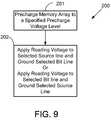
- FIG. 9is a flow diagram of an illustrative method of reading a memory unit array 200 , described above.
- the methodincludes precharging the memory array to a specified precharge voltage level at block 201 , as described above. Then a reading current is applied to either the selected source or bit line and the other selected source or bit line is grounded at block 202 .
Landscapes
- Engineering & Computer Science (AREA)
- Computer Hardware Design (AREA)
- Mram Or Spin Memory Techniques (AREA)
- Hall/Mr Elements (AREA)
Abstract
Description
Claims (12)
Priority Applications (3)
| Application Number | Priority Date | Filing Date | Title |
|---|---|---|---|
| US12/254,414US7936580B2 (en) | 2008-10-20 | 2008-10-20 | MRAM diode array and access method |
| US12/948,824US8289746B2 (en) | 2008-10-20 | 2010-11-18 | MRAM diode array and access method |
| US13/611,225US8514605B2 (en) | 2008-10-20 | 2012-09-12 | MRAM diode array and access method |
Applications Claiming Priority (1)
| Application Number | Priority Date | Filing Date | Title |
|---|---|---|---|
| US12/254,414US7936580B2 (en) | 2008-10-20 | 2008-10-20 | MRAM diode array and access method |
Related Child Applications (1)
| Application Number | Title | Priority Date | Filing Date |
|---|---|---|---|
| US12/948,824ContinuationUS8289746B2 (en) | 2008-10-20 | 2010-11-18 | MRAM diode array and access method |
Publications (2)
| Publication Number | Publication Date |
|---|---|
| US20100097852A1 US20100097852A1 (en) | 2010-04-22 |
| US7936580B2true US7936580B2 (en) | 2011-05-03 |
Family
ID=42108551
Family Applications (3)
| Application Number | Title | Priority Date | Filing Date |
|---|---|---|---|
| US12/254,414Expired - Fee RelatedUS7936580B2 (en) | 2008-10-20 | 2008-10-20 | MRAM diode array and access method |
| US12/948,824Expired - Fee RelatedUS8289746B2 (en) | 2008-10-20 | 2010-11-18 | MRAM diode array and access method |
| US13/611,225ActiveUS8514605B2 (en) | 2008-10-20 | 2012-09-12 | MRAM diode array and access method |
Family Applications After (2)
| Application Number | Title | Priority Date | Filing Date |
|---|---|---|---|
| US12/948,824Expired - Fee RelatedUS8289746B2 (en) | 2008-10-20 | 2010-11-18 | MRAM diode array and access method |
| US13/611,225ActiveUS8514605B2 (en) | 2008-10-20 | 2012-09-12 | MRAM diode array and access method |
Country Status (1)
| Country | Link |
|---|---|
| US (3) | US7936580B2 (en) |
Cited By (3)
| Publication number | Priority date | Publication date | Assignee | Title |
|---|---|---|---|---|
| US9614002B1 (en)* | 2016-01-21 | 2017-04-04 | Samsung Electronics Co., Ltd. | 0T bi-directional memory cell |
| US9853053B2 (en) | 2012-09-10 | 2017-12-26 | 3B Technologies, Inc. | Three dimension integrated circuits employing thin film transistors |
| US10475815B2 (en) | 2013-09-09 | 2019-11-12 | Tacho Holdings, Llc | Three dimension integrated circuits employing thin film transistors |
Families Citing this family (25)
| Publication number | Priority date | Publication date | Assignee | Title |
|---|---|---|---|---|
| US7953462B2 (en) | 2008-08-04 | 2011-05-31 | Vartanian Harry | Apparatus and method for providing an adaptively responsive flexible display device |
| US7936580B2 (en)* | 2008-10-20 | 2011-05-03 | Seagate Technology Llc | MRAM diode array and access method |
| US7969767B2 (en)* | 2009-05-29 | 2011-06-28 | Qualcomm Incorporated | Spin transfer torque—magnetic tunnel junction device and method of operation |
| US8638590B2 (en) | 2010-09-28 | 2014-01-28 | Qualcomm Incorporated | Resistance based memory having two-diode access device |
| FR2973149B1 (en)* | 2011-03-24 | 2021-12-10 | Univ Paris Sud 11 | LOGICAL MEMORY ARCHITECTURE, ESPECIALLY FOR MRAM OR PCRAM OR RRAM. |
| US8952470B2 (en) | 2012-09-10 | 2015-02-10 | James John Lupino | Low cost high density nonvolatile memory array device employing thin film transistors and back to back Schottky diodes |
| US20140124880A1 (en) | 2012-11-06 | 2014-05-08 | International Business Machines Corporation | Magnetoresistive random access memory |
| US8750033B2 (en) | 2012-11-06 | 2014-06-10 | International Business Machines Corporation | Reading a cross point cell array |
| US9076523B2 (en)* | 2012-12-13 | 2015-07-07 | Intermolecular, Inc. | Methods of manufacturing embedded bipolar switching resistive memory |
| KR102023626B1 (en) | 2013-01-25 | 2019-09-20 | 삼성전자 주식회사 | Memory device using spin hall effect and methods of manufacturing and operating the same |
| EP2814073B1 (en)* | 2013-06-14 | 2017-02-15 | IMEC vzw | Self-rectifying RRAM element |
| US20150070983A1 (en)* | 2013-09-09 | 2015-03-12 | Yoshinori Kumura | Magnetic memory device |
| KR102189684B1 (en) | 2013-12-05 | 2020-12-11 | 삼성전자주식회사 | Method of operating semiconductor memory devices |
| TWI559450B (en) | 2014-04-18 | 2016-11-21 | 力晶科技股份有限公司 | Memory structure and its operation method |
| US9418761B2 (en) | 2014-12-12 | 2016-08-16 | Intel Corporation | Apparatus for boosting source-line voltage to reduce leakage in resistive memories |
| JP6178451B1 (en)* | 2016-03-16 | 2017-08-09 | 株式会社東芝 | Memory cell and magnetic memory |
| US9858975B1 (en)* | 2016-08-24 | 2018-01-02 | Samsung Electronics Co., Ltd. | Zero transistor transverse current bi-directional bitcell |
| US10381060B2 (en)* | 2016-08-25 | 2019-08-13 | Qualcomm Incorporated | High-speed, low power spin-orbit torque (SOT) assisted spin-transfer torque magnetic random access memory (STT-MRAM) bit cell array |
| US20200027491A1 (en)* | 2016-12-19 | 2020-01-23 | Agency For Science, Technology And Research | Memory cell, methods of forming and operating the same |
| US10127960B1 (en)* | 2017-05-12 | 2018-11-13 | Avalanche Technology, Inc. | Transient sensing of memory cells |
| US10790002B2 (en) | 2018-06-21 | 2020-09-29 | Samsung Electronics Co., Ltd. | Giant spin hall-based compact neuromorphic cell optimized for differential read inference |
| US10991756B2 (en)* | 2018-10-23 | 2021-04-27 | Taiwan Semiconductor Manufacturing Co., Ltd. | Bipolar selector with independently tunable threshold voltages |
| US10832751B2 (en) | 2018-10-31 | 2020-11-10 | Avalanche Technology, Inc. | Magnetic memory and method for using the same |
| US11107859B2 (en)* | 2019-08-05 | 2021-08-31 | Taiwan Semiconductor Manufacturing Company, Ltd. | Memory cell with unipolar selectors |
| US11610616B2 (en) | 2020-06-12 | 2023-03-21 | Avalanche Technology, Inc. | Locally timed sensing of memory device |
Citations (144)
| Publication number | Priority date | Publication date | Assignee | Title |
|---|---|---|---|---|
| US3982235A (en) | 1974-08-28 | 1976-09-21 | The United States Of America As Represented By The Secretary Of The Navy | Sinusoidal film plated memory wire |
| US3982233A (en) | 1974-02-19 | 1976-09-21 | Ampex Corporation | Core memory with improved sense-inhibit recovery time |
| US4160988A (en) | 1974-03-26 | 1979-07-10 | Signetics Corporation | Integrated injection logic (I-squared L) with double-diffused type injector |
| US4232057A (en) | 1979-03-01 | 1980-11-04 | International Business Machines Corporation | Semiconductor plasma oxidation |
| US4247915A (en) | 1979-01-02 | 1981-01-27 | Texas Instruments Incorporated | Punch-through load devices in high density static memory cell |
| US4323589A (en) | 1980-05-07 | 1982-04-06 | International Business Machines Corporation | Plasma oxidation |
| US4576829A (en) | 1984-12-28 | 1986-03-18 | Rca Corporation | Low temperature growth of silicon dioxide on silicon |
| US4901132A (en) | 1986-06-09 | 1990-02-13 | Texas Instruments Incorporated | Semiconductor integrated circuit with switching bipolar transistors having high withstand voltage capability |
| US5083190A (en) | 1989-09-05 | 1992-01-21 | Motorola, Inc. | Shared gate CMOS transistor |
| US5135878A (en) | 1990-08-28 | 1992-08-04 | Solid State Devices, Inc. | Schottky diode |
| US5278636A (en) | 1989-09-29 | 1994-01-11 | The United States Of America As Represented By The Administrator Of The National Aeronautics And Space Administration | Non-volatile, solid state bistable electrical switch |
| US5330935A (en) | 1990-10-24 | 1994-07-19 | International Business Machines Corporation | Low temperature plasma oxidation process |
| US5365083A (en) | 1990-11-29 | 1994-11-15 | Kawasaki Steel Corporation | Semiconductor device of band-to-band tunneling type |
| US5443863A (en) | 1994-03-16 | 1995-08-22 | Auburn University | Low-temperature oxidation at surfaces using ozone decomposition products formed by microwave discharge |
| US5580804A (en) | 1994-12-15 | 1996-12-03 | Advanced Micro Devices, Inc. | Method for fabricating true LDD devices in a MOS technology |
| US5614430A (en) | 1996-03-11 | 1997-03-25 | Taiwan Semiconductor Manufacturing Company Ltd. | Anti-punchthrough ion implantation for sub-half micron channel length MOSFET devices |
| US5739564A (en) | 1992-12-11 | 1998-04-14 | Motorola, Inc. | Semiconductor device having a static-random-access memory cell |
| US5872052A (en) | 1996-02-12 | 1999-02-16 | Micron Technology, Inc. | Planarization using plasma oxidized amorphous silicon |
| US5913149A (en) | 1992-12-31 | 1999-06-15 | Micron Technology, Inc. | Method for fabricating stacked layer silicon nitride for low leakage and high capacitance |
| US5923948A (en) | 1994-11-04 | 1999-07-13 | Micron Technology, Inc. | Method for sharpening emitter sites using low temperature oxidation processes |
| US5926412A (en) | 1992-02-09 | 1999-07-20 | Raytheon Company | Ferroelectric memory structure |
| US5929477A (en) | 1997-01-22 | 1999-07-27 | International Business Machines Corporation | Self-aligned diffused source vertical transistors with stack capacitors in a 4F-square memory cell array |
| US6011281A (en) | 1997-12-02 | 2000-01-04 | Fujitsu Quantum Devices Limited | Semiconductor device having an ohmic contact and a Schottky contact, with a barrier layer interposed between the ohmic contact and the Schottky contact |
| US6013548A (en) | 1997-01-22 | 2000-01-11 | International Business Machines Corporation | Self-aligned diffused source vertical transistors with deep trench capacitors in a 4F-square memory cell array |
| US6100166A (en) | 1996-12-18 | 2000-08-08 | Canon Kabushiki Kaisha | Process for producing semiconductor article |
| US6114211A (en) | 1998-11-18 | 2000-09-05 | Advanced Micro Devices, Inc. | Semiconductor device with vertical halo region and methods of manufacture |
| US6121642A (en) | 1998-07-20 | 2000-09-19 | International Business Machines Corporation | Junction mott transition field effect transistor (JMTFET) and switch for logic and memory applications |
| US6121654A (en) | 1997-10-10 | 2000-09-19 | The Research Foundation Of State University Of New York | Memory device having a crested tunnel barrier |
| US6165834A (en) | 1998-05-07 | 2000-12-26 | Micron Technology, Inc. | Method of forming capacitors, method of processing dielectric layers, method of forming a DRAM cell |
| US6300205B1 (en) | 1998-11-18 | 2001-10-09 | Advanced Micro Devices, Inc. | Method of making a semiconductor device with self-aligned active, lightly-doped drain, and halo regions |
| US6341085B1 (en) | 1991-11-26 | 2002-01-22 | Hitachi, Ltd. | Storage device employing a flash memory |
| US6346477B1 (en) | 2001-01-09 | 2002-02-12 | Research Foundation Of Suny - New York | Method of interlayer mediated epitaxy of cobalt silicide from low temperature chemical vapor deposition of cobalt |
| US6376332B1 (en) | 1999-02-02 | 2002-04-23 | Canon Kabushiki Kaisha | Composite member and separating method therefor, bonded substrate stack and separating method therefor, transfer method for transfer layer, and SOI substrate manufacturing method |
| US6448840B2 (en) | 1999-11-30 | 2002-09-10 | Intel Corporation | Adaptive body biasing circuit and method |
| US20020136047A1 (en) | 2001-03-21 | 2002-09-26 | Scheuerlein Roy E. | Method and apparatus for biasing selected and unselected array lines when writing a memory array |
| US20030045064A1 (en)* | 2001-09-05 | 2003-03-06 | Mitsubishi Denki Kabushiki Kaisha | Semiconductor device comprising sense amplifier and manufacturing method thereof |
| EP1329895A2 (en) | 2002-01-08 | 2003-07-23 | SAMSUNG ELECTRONICS Co. Ltd. | High-density magnetic random access memory device and method of operating the same |
| US6617642B1 (en) | 2000-02-23 | 2003-09-09 | Tripath Technology, Inc. | Field effect transistor structure for driving inductive loads |
| US20030168684A1 (en) | 2002-01-31 | 2003-09-11 | Sharp Laboratories Of America, Inc. | Method of fabricating magnetic yoke structures in MRAM devices |
| US6624463B2 (en) | 2001-09-17 | 2003-09-23 | Hyun-Tak Kim | Switching field effect transistor using abrupt metal-insulator transition |
| US6653704B1 (en) | 2002-09-24 | 2003-11-25 | International Business Machines Corporation | Magnetic memory with tunnel junction memory cells and phase transition material for controlling current to the cells |
| US6667900B2 (en) | 2001-12-28 | 2003-12-23 | Ovonyx, Inc. | Method and apparatus to operate a memory cell |
| US20040084725A1 (en) | 2002-11-01 | 2004-05-06 | Toyota Jidosha Kabushiki Kaisha | Field-effect-type semiconductor device |
| US6750540B2 (en) | 2001-12-26 | 2004-06-15 | Hynix Semiconductor Inc. | Magnetic random access memory using schottky diode |
| US20040114413A1 (en) | 2002-12-13 | 2004-06-17 | Parkinson Ward D. | Memory and access devices |
| US20040114438A1 (en) | 2002-12-05 | 2004-06-17 | Sharp Kabushiki Kaisha | Semiconductor memory device and erase method for memory array |
| US6753561B1 (en) | 2002-08-02 | 2004-06-22 | Unity Semiconductor Corporation | Cross point memory array using multiple thin films |
| US6757842B2 (en) | 1989-04-13 | 2004-06-29 | Sandisk Corporation | Flash EEprom system |
| US6781176B2 (en) | 2000-08-31 | 2004-08-24 | University Of Maryland | Conductively doped strontium titanate barrier intermediate a silicon underlayer and an epitaxial metal oxide film |
| US6789689B1 (en) | 1997-12-17 | 2004-09-14 | B & R Industries Pty Ltd | Container with multiple integral connection handle, preform and method of manufacture |
| US6800897B2 (en) | 2001-04-11 | 2004-10-05 | Silicon Semiconductor Corporation | Integrated circuit power devices having junction barrier controlled schottky diodes therein |
| US20040257878A1 (en) | 2003-05-20 | 2004-12-23 | Yoshinao Morikawa | Semiconductor storage device and mobile electronic apparatus |
| US20040262635A1 (en) | 2003-06-24 | 2004-12-30 | Sang-Yun Lee | Three-dimensional integrated circuit structure and method of making same |
| US6842368B2 (en) | 2002-11-28 | 2005-01-11 | Hitachi, Ltd. | High output nonvolatile magnetic memory |
| US20050044703A1 (en) | 2003-08-26 | 2005-03-03 | Li-Wen Liu | Method of producing an led rope light |
| US20050092526A1 (en) | 2003-11-03 | 2005-05-05 | Fielder Coy M. | Expandable eccentric reamer and method of use in drilling |
| US20050122768A1 (en) | 2003-09-12 | 2005-06-09 | Sharp Kabushiki Kaisha | Nonvolatile semiconductor memory device |
| US20050145947A1 (en) | 2000-11-06 | 2005-07-07 | Russ Cornelius C. | Silicon controlled rectifier electrostatic discharge protection device for power supply lines with powerdown mode of operation |
| US6917539B2 (en) | 2002-08-02 | 2005-07-12 | Unity Semiconductor Corporation | High-density NVRAM |
| US6940742B2 (en) | 2003-04-10 | 2005-09-06 | Seiko Epson Corporation | Method of storing data in ferroelectric memory device |
| US6944052B2 (en) | 2002-11-26 | 2005-09-13 | Freescale Semiconductor, Inc. | Magnetoresistive random access memory (MRAM) cell having a diode with asymmetrical characteristics |
| US20050218521A1 (en) | 2004-06-21 | 2005-10-06 | Sang-Yun Lee | Electronic circuit with embedded memory |
| US20050253143A1 (en) | 2002-01-22 | 2005-11-17 | Renesas Technology Corporation | Semiconductor memory device using vertical-channel transistors |
| US20050280155A1 (en) | 2004-06-21 | 2005-12-22 | Sang-Yun Lee | Semiconductor bonding and layer transfer method |
| US20050280154A1 (en) | 2004-06-21 | 2005-12-22 | Sang-Yun Lee | Semiconductor memory device |
| US20050282356A1 (en) | 2004-06-21 | 2005-12-22 | Sang-Yun Lee | Semiconductor layer structure and method of making the same |
| US20050280061A1 (en) | 2004-06-21 | 2005-12-22 | Sang-Yun Lee | Vertical memory device structures |
| US20050280156A1 (en) | 2004-06-21 | 2005-12-22 | Sang-Yun Lee | Semiconductor device with base support structure |
| US20050280042A1 (en) | 2004-06-21 | 2005-12-22 | Sang-Yun Lee | Wafer bonding method |
| US6979863B2 (en) | 2003-04-24 | 2005-12-27 | Cree, Inc. | Silicon carbide MOSFETs with integrated antiparallel junction barrier Schottky free wheeling diodes and methods of fabricating the same |
| US7009877B1 (en) | 2003-11-14 | 2006-03-07 | Grandis, Inc. | Three-terminal magnetostatically coupled spin transfer-based MRAM cell |
| US20060073652A1 (en) | 2004-09-17 | 2006-04-06 | Fabio Pellizzer | Phase change memory with ovonic threshold switch |
| US7045840B2 (en) | 2003-12-04 | 2006-05-16 | Sharp Kabushiki Kaisha | Nonvolatile semiconductor memory device comprising a variable resistive element containing a perovskite-type crystal structure |
| US7051941B2 (en) | 2003-03-03 | 2006-05-30 | Nisca Corporation | Image reading unit and image reading apparatus |
| US20060131554A1 (en) | 2004-12-21 | 2006-06-22 | Young-Soo Joung | Nonvolatile memory device having two or more resistance elements and methods of forming and using the same |
| US7098494B2 (en) | 2004-06-16 | 2006-08-29 | Grandis, Inc. | Re-configurable logic elements using heat assisted magnetic tunneling elements |
| US7130209B2 (en) | 2004-10-15 | 2006-10-31 | Atmel Corporation | Flexible OTP sector protection architecture for flash memories |
| US7161861B2 (en) | 2004-11-15 | 2007-01-09 | Infineon Technologies Ag | Sense amplifier bitline boost circuit |
| US20070007536A1 (en) | 2001-04-26 | 2007-01-11 | Renesas Technology Corporation | Thin film magnetic memory device capable of conducting stable data read and write operations |
| US7180140B1 (en) | 2004-04-16 | 2007-02-20 | National Semiconductor Corporation | PMOS device with drain junction breakdown point located for reduced drain breakdown voltage walk-in and method for designing and manufacturing such device |
| US7187577B1 (en) | 2005-11-23 | 2007-03-06 | Grandis, Inc. | Method and system for providing current balanced writing for memory cells and magnetic devices |
| US7190616B2 (en) | 2004-07-19 | 2007-03-13 | Micron Technology, Inc. | In-service reconfigurable DRAM and flash memory device |
| US7200036B2 (en) | 2004-11-26 | 2007-04-03 | Sony Corporation | Memory including a transfer gate and a storage element |
| US20070077694A1 (en) | 2003-06-24 | 2007-04-05 | Sang-Yun Lee | Three-dimensional integrated circuit structure |
| US7215568B2 (en) | 2004-08-30 | 2007-05-08 | Infineon Technologies Ag | Resistive memory arrangement |
| US20070105241A1 (en) | 2004-07-30 | 2007-05-10 | Rainer Leuschner | Ferromagnetic liner for conductive lines of magnetic memory cells |
| US7218550B2 (en) | 1998-10-30 | 2007-05-15 | Nikolai Franz Gregor Schwabe | Magnetic storage device |
| US20070115749A1 (en) | 2005-10-14 | 2007-05-24 | Axon Technologies Corporation | Voltage reference circuit using programmable metallization cells |
| US20070113884A1 (en) | 2005-11-18 | 2007-05-24 | Kinsey Geoffrey S | Monolithic bypass diode and photovoltaic cell with bypass diode formed in back of substrate |
| US7224601B2 (en) | 2005-08-25 | 2007-05-29 | Grandis Inc. | Oscillating-field assisted spin torque switching of a magnetic tunnel junction memory element |
| US7233537B2 (en) | 2002-04-03 | 2007-06-19 | Renesas Technology Corp. | Thin film magnetic memory device provided with a dummy cell for data read reference |
| US7236394B2 (en) | 2003-06-18 | 2007-06-26 | Macronix International Co., Ltd. | Transistor-free random access memory |
| US7247570B2 (en) | 2004-08-19 | 2007-07-24 | Micron Technology, Inc. | Silicon pillars for vertical transistors |
| US7272035B1 (en) | 2005-08-31 | 2007-09-18 | Grandis, Inc. | Current driven switching of magnetic storage cells utilizing spin transfer and magnetic memories using such cells |
| US7272034B1 (en) | 2005-08-31 | 2007-09-18 | Grandis, Inc. | Current driven switching of magnetic storage cells utilizing spin transfer and magnetic memories using such cells |
| US7274067B2 (en) | 2001-08-30 | 2007-09-25 | Micron Technology, Inc. | Service programmable logic arrays with low tunnel barrier interpoly insulators |
| US7273638B2 (en) | 2003-01-07 | 2007-09-25 | International Business Machines Corp. | High density plasma oxidation |
| US7282755B2 (en) | 2003-11-14 | 2007-10-16 | Grandis, Inc. | Stress assisted current driven switching for magnetic memory applications |
| US7286395B2 (en) | 2005-10-27 | 2007-10-23 | Grandis, Inc. | Current driven switched magnetic storage cells having improved read and write margins and magnetic memories using such cells |
| US7285812B2 (en) | 2004-09-02 | 2007-10-23 | Micron Technology, Inc. | Vertical transistors |
| US7289356B2 (en) | 2005-06-08 | 2007-10-30 | Grandis, Inc. | Fast magnetic memory devices utilizing spin transfer and magnetic elements used therein |
| US20070253245A1 (en) | 2006-04-27 | 2007-11-01 | Yadav Technology | High Capacity Low Cost Multi-Stacked Cross-Line Magnetic Memory |
| US20070281439A1 (en) | 2003-10-15 | 2007-12-06 | International Business Machines Corporation | Techniques for Layer Transfer Processing |
| US20070279968A1 (en) | 2006-06-01 | 2007-12-06 | Xiao Luo | Method and system for providing a magnetic memory structure utilizing spin transfer |
| US20070297223A1 (en) | 2006-06-26 | 2007-12-27 | Eugene Youjun Chen | Current driven switching of magnetic storage cells utilizing spin transfer and magnetic memories using such cells having enhanced read and write margins |
| US20080007993A1 (en) | 2006-07-04 | 2008-01-10 | Sharp Kabushiki Kaisha | Semiconductor memory device |
| US20080029782A1 (en) | 2006-08-04 | 2008-02-07 | Texas Instruments, Inc. | Integrated ESD protection device |
| US20080037314A1 (en) | 2006-08-09 | 2008-02-14 | Yoshihiro Ueda | Magnetic memory |
| US20080094873A1 (en) | 2006-10-23 | 2008-04-24 | Macronix International Co., Ltd. | Method and Apparatus for Non-Volatile Multi-Bit Memory |
| US20080108212A1 (en) | 2006-10-19 | 2008-05-08 | Atmel Corporation | High voltage vertically oriented eeprom device |
| US7381595B2 (en) | 2004-03-15 | 2008-06-03 | Sharp Laboratories Of America, Inc. | High-density plasma oxidation for enhanced gate oxide performance |
| US7382024B2 (en) | 2004-08-05 | 2008-06-03 | Broadcom Corporation | Low threshold voltage PMOS apparatus and method of fabricating the same |
| US20080144355A1 (en) | 2004-11-30 | 2008-06-19 | Koninklijke Philips Electronics N.V. | Dielectric Antifuse for Electro-Thermally Programmable Device |
| US20080170432A1 (en) | 2007-01-17 | 2008-07-17 | Yoshiaki Asao | Magnetic random access memory and write method of the same |
| US20080191312A1 (en) | 2003-06-24 | 2008-08-14 | Oh Choonsik | Semiconductor circuit |
| US7414908B2 (en) | 2003-12-03 | 2008-08-19 | International Business Machines Corporation | Magnetic memory device |
| US7416929B2 (en) | 2004-07-08 | 2008-08-26 | Semisouth Laboratories, Inc. | Monolithic vertical junction field effect transistor and schottky barrier diode fabricated from silicon carbide and method for fabricating the same |
| US7432574B2 (en) | 2006-03-29 | 2008-10-07 | Kabushiki Kaisha Toshiba | Magnetic recording element and magnetic memory |
| US7440317B2 (en) | 2002-08-30 | 2008-10-21 | Micron Technology, Inc. | One transistor SOI non-volatile random access memory cell |
| US20080273380A1 (en) | 2007-03-27 | 2008-11-06 | Grandis | Method and system for providing field biased magnetic memory devices |
| US7464629B2 (en) | 2004-03-01 | 2008-12-16 | Societe Commerciale Rusch | Lathe tool |
| US7465983B2 (en) | 2001-08-30 | 2008-12-16 | Micron Technology, Inc. | Low tunnel barrier insulators |
| US20080310213A1 (en) | 2007-06-15 | 2008-12-18 | Grandis, Inc. | Method and system for providing spin transfer tunneling magnetic memories utilizing non-planar transistors |
| US20080310219A1 (en) | 2007-06-12 | 2008-12-18 | Grandis, Inc. | Method and system for providing a magnetic element and magnetic memory being unidirectional writing enabled |
| US20090014719A1 (en) | 2007-07-13 | 2009-01-15 | Renesas Technology Corp. | Semiconductor device with large blocking voltage |
| US20090040855A1 (en) | 2007-08-07 | 2009-02-12 | Grandis, Inc. | Method and system for providing a sense amplifier and drive circuit for spin transfer torque magnetic random access memory |
| US20090052225A1 (en) | 2005-01-24 | 2009-02-26 | Hidenori Morimoto | Nonvolatile Semiconductor Memory Device |
| US7502249B1 (en) | 2006-07-17 | 2009-03-10 | Grandis, Inc. | Method and system for using a pulsed field to assist spin transfer induced switching of magnetic memory elements |
| US20090072246A1 (en) | 2007-09-18 | 2009-03-19 | Samsung Electronics Co., Ltd. | Diode and memory device comprising the same |
| US20090072279A1 (en) | 2007-08-29 | 2009-03-19 | Ecole Polytechnique Federale De Lausanne (Epfl) | Capacitor-less memory and abrupt switch based on hysteresis characteristics in punch-through impact ionization mos transistor (PI-MOS) |
| US7515457B2 (en) | 2006-02-24 | 2009-04-07 | Grandis, Inc. | Current driven memory cells having enhanced current and enhanced current symmetry |
| US7542356B2 (en) | 2006-11-01 | 2009-06-02 | Samsung Electronics Co., Ltd. | Semiconductor memory device and method for reducing cell activation during write operations |
| US20090162979A1 (en) | 2001-03-22 | 2009-06-25 | Yang Kevin J | Thyristor device with carbon lifetime adjustment implant and its method of fabrication |
| US20090161408A1 (en) | 2006-12-08 | 2009-06-25 | Sharp Kabushiki Kaisha | Semiconductor memory device |
| US20090185410A1 (en) | 2008-01-22 | 2009-07-23 | Grandis, Inc. | Method and system for providing spin transfer tunneling magnetic memories utilizing unidirectional polarity selection devices |
| US20090296449A1 (en) | 2008-06-02 | 2009-12-03 | Stefan Slesazeck | Integrated Circuit and Method of Operating an Integrated Circuit |
| DE102008026432A1 (en) | 2008-06-02 | 2009-12-10 | Qimonda Ag | Integrated circuit for use in e.g. magnetoresistive RAM module, has set of resistance change memory elements, and set of memory element selection devices that are floating-body-selection devices such as FETs or thyristors |
| US20100007344A1 (en) | 2008-07-08 | 2010-01-14 | Magic Technologies, Inc. | MTJ based magnetic field sensor with ESD shunt trace |
| US20100067281A1 (en) | 2008-09-15 | 2010-03-18 | Seagate Technology Llc | Variable write and read methods for resistive random access memory |
| US20100078620A1 (en) | 2008-09-30 | 2010-04-01 | Seagate Technology Llc | Semiconductor device with thermally coupled phase change layers |
| US20100110756A1 (en) | 2008-10-30 | 2010-05-06 | Seagate Technology Llc | Variable resistive memory punchthrough access method |
| US7732881B2 (en) | 2006-11-01 | 2010-06-08 | Avalanche Technology, Inc. | Current-confined effect of magnetic nano-current-channel (NCC) for magnetic random access memory (MRAM) |
| US20100142256A1 (en) | 2008-06-27 | 2010-06-10 | Sandisk 3D Llc | Method of programming a nonvolatile memory cell by reverse biasing a diode steering element to set a storage element |
| US20100149856A1 (en) | 2008-12-12 | 2010-06-17 | Stephen Tang | Writing Memory Cells Exhibiting Threshold Switch Behavior |
Family Cites Families (12)
| Publication number | Priority date | Publication date | Assignee | Title |
|---|---|---|---|---|
| US3746945A (en) | 1971-10-27 | 1973-07-17 | Motorola Inc | Schottky diode clipper device |
| US5341114A (en) | 1990-11-02 | 1994-08-23 | Ail Systems, Inc. | Integrated limiter and amplifying devices |
| US6043527A (en) | 1998-04-14 | 2000-03-28 | Micron Technology, Inc. | Circuits and methods for a memory cell with a trench plate trench capacitor and a vertical bipolar read device |
| JP2003101036A (en) | 2001-09-25 | 2003-04-04 | Sanyo Electric Co Ltd | Schottky barrier diode and method of manufacturing the same |
| US7738881B2 (en) | 2003-07-22 | 2010-06-15 | Microsoft Corporation | Systems for determining the approximate location of a device from ambient signals |
| NO324607B1 (en) | 2003-11-24 | 2007-11-26 | Thin Film Electronics Asa | Method of operating a data storage device using passive matrix addressing |
| KR100593450B1 (en) | 2004-10-08 | 2006-06-28 | 삼성전자주식회사 | P having a plurality of active regions located vertically in turn. Rams and methods of forming the same. |
| US8179711B2 (en) | 2004-10-26 | 2012-05-15 | Samsung Electronics Co., Ltd. | Semiconductor memory device with stacked memory cell and method of manufacturing the stacked memory cell |
| US7301803B2 (en) | 2004-12-22 | 2007-11-27 | Innovative Silicon S.A. | Bipolar reading technique for a memory cell having an electrically floating body transistor |
| KR100885184B1 (en) | 2007-01-30 | 2009-02-23 | 삼성전자주식회사 | Memory device having resistance characteristics that can be controlled independently by electric and magnetic fields, and method of operation thereof |
| US7697322B2 (en) | 2007-07-10 | 2010-04-13 | Qimonda Ag | Integrated circuits; method for manufacturing an integrated circuit; method for decreasing the influence of magnetic fields; memory module |
| US7936580B2 (en)* | 2008-10-20 | 2011-05-03 | Seagate Technology Llc | MRAM diode array and access method |
- 2008
- 2008-10-20USUS12/254,414patent/US7936580B2/ennot_activeExpired - Fee Related
- 2010
- 2010-11-18USUS12/948,824patent/US8289746B2/ennot_activeExpired - Fee Related
- 2012
- 2012-09-12USUS13/611,225patent/US8514605B2/enactiveActive
Patent Citations (165)
| Publication number | Priority date | Publication date | Assignee | Title |
|---|---|---|---|---|
| US3982233A (en) | 1974-02-19 | 1976-09-21 | Ampex Corporation | Core memory with improved sense-inhibit recovery time |
| US4160988A (en) | 1974-03-26 | 1979-07-10 | Signetics Corporation | Integrated injection logic (I-squared L) with double-diffused type injector |
| US3982235A (en) | 1974-08-28 | 1976-09-21 | The United States Of America As Represented By The Secretary Of The Navy | Sinusoidal film plated memory wire |
| US4247915A (en) | 1979-01-02 | 1981-01-27 | Texas Instruments Incorporated | Punch-through load devices in high density static memory cell |
| US4232057A (en) | 1979-03-01 | 1980-11-04 | International Business Machines Corporation | Semiconductor plasma oxidation |
| US4323589A (en) | 1980-05-07 | 1982-04-06 | International Business Machines Corporation | Plasma oxidation |
| US4576829A (en) | 1984-12-28 | 1986-03-18 | Rca Corporation | Low temperature growth of silicon dioxide on silicon |
| US4901132A (en) | 1986-06-09 | 1990-02-13 | Texas Instruments Incorporated | Semiconductor integrated circuit with switching bipolar transistors having high withstand voltage capability |
| US7397713B2 (en) | 1989-04-13 | 2008-07-08 | Sandisk Corporation | Flash EEprom system |
| US7362618B2 (en) | 1989-04-13 | 2008-04-22 | Sandisk Corporation | Flash EEprom system |
| US6757842B2 (en) | 1989-04-13 | 2004-06-29 | Sandisk Corporation | Flash EEprom system |
| US5083190A (en) | 1989-09-05 | 1992-01-21 | Motorola, Inc. | Shared gate CMOS transistor |
| US5278636A (en) | 1989-09-29 | 1994-01-11 | The United States Of America As Represented By The Administrator Of The National Aeronautics And Space Administration | Non-volatile, solid state bistable electrical switch |
| US5135878A (en) | 1990-08-28 | 1992-08-04 | Solid State Devices, Inc. | Schottky diode |
| US5330935A (en) | 1990-10-24 | 1994-07-19 | International Business Machines Corporation | Low temperature plasma oxidation process |
| US5412246A (en) | 1990-10-24 | 1995-05-02 | International Business Machines Corporation | Low temperature plasma oxidation process |
| US5365083A (en) | 1990-11-29 | 1994-11-15 | Kawasaki Steel Corporation | Semiconductor device of band-to-band tunneling type |
| US6341085B1 (en) | 1991-11-26 | 2002-01-22 | Hitachi, Ltd. | Storage device employing a flash memory |
| US5926412A (en) | 1992-02-09 | 1999-07-20 | Raytheon Company | Ferroelectric memory structure |
| US5739564A (en) | 1992-12-11 | 1998-04-14 | Motorola, Inc. | Semiconductor device having a static-random-access memory cell |
| US5913149A (en) | 1992-12-31 | 1999-06-15 | Micron Technology, Inc. | Method for fabricating stacked layer silicon nitride for low leakage and high capacitance |
| US5443863A (en) | 1994-03-16 | 1995-08-22 | Auburn University | Low-temperature oxidation at surfaces using ozone decomposition products formed by microwave discharge |
| US5923948A (en) | 1994-11-04 | 1999-07-13 | Micron Technology, Inc. | Method for sharpening emitter sites using low temperature oxidation processes |
| US5580804A (en) | 1994-12-15 | 1996-12-03 | Advanced Micro Devices, Inc. | Method for fabricating true LDD devices in a MOS technology |
| US5872052A (en) | 1996-02-12 | 1999-02-16 | Micron Technology, Inc. | Planarization using plasma oxidized amorphous silicon |
| US5614430A (en) | 1996-03-11 | 1997-03-25 | Taiwan Semiconductor Manufacturing Company Ltd. | Anti-punchthrough ion implantation for sub-half micron channel length MOSFET devices |
| US6100166A (en) | 1996-12-18 | 2000-08-08 | Canon Kabushiki Kaisha | Process for producing semiconductor article |
| US6534382B1 (en) | 1996-12-18 | 2003-03-18 | Canon Kabushiki Kaisha | Process for producing semiconductor article |
| US6077745A (en) | 1997-01-22 | 2000-06-20 | International Business Machines Corporation | Self-aligned diffused source vertical transistors with stack capacitors in a 4F-square memory cell array |
| US6034389A (en) | 1997-01-22 | 2000-03-07 | International Business Machines Corporation | Self-aligned diffused source vertical transistors with deep trench capacitors in a 4F-square memory cell array |
| US6013548A (en) | 1997-01-22 | 2000-01-11 | International Business Machines Corporation | Self-aligned diffused source vertical transistors with deep trench capacitors in a 4F-square memory cell array |
| US5929477A (en) | 1997-01-22 | 1999-07-27 | International Business Machines Corporation | Self-aligned diffused source vertical transistors with stack capacitors in a 4F-square memory cell array |
| US6121654A (en) | 1997-10-10 | 2000-09-19 | The Research Foundation Of State University Of New York | Memory device having a crested tunnel barrier |
| US6011281A (en) | 1997-12-02 | 2000-01-04 | Fujitsu Quantum Devices Limited | Semiconductor device having an ohmic contact and a Schottky contact, with a barrier layer interposed between the ohmic contact and the Schottky contact |
| US6789689B1 (en) | 1997-12-17 | 2004-09-14 | B & R Industries Pty Ltd | Container with multiple integral connection handle, preform and method of manufacture |
| US6165834A (en) | 1998-05-07 | 2000-12-26 | Micron Technology, Inc. | Method of forming capacitors, method of processing dielectric layers, method of forming a DRAM cell |
| US6121642A (en) | 1998-07-20 | 2000-09-19 | International Business Machines Corporation | Junction mott transition field effect transistor (JMTFET) and switch for logic and memory applications |
| US7218550B2 (en) | 1998-10-30 | 2007-05-15 | Nikolai Franz Gregor Schwabe | Magnetic storage device |
| US6300205B1 (en) | 1998-11-18 | 2001-10-09 | Advanced Micro Devices, Inc. | Method of making a semiconductor device with self-aligned active, lightly-doped drain, and halo regions |
| US6114211A (en) | 1998-11-18 | 2000-09-05 | Advanced Micro Devices, Inc. | Semiconductor device with vertical halo region and methods of manufacture |
| US20020081822A1 (en) | 1999-02-02 | 2002-06-27 | Kazutaka Yanagita | Composite member and separating method therefor, bonded substrate stack and separating method therefor, transfer method for transfer layer, and SOI substrate manufacturing method |
| US6376332B1 (en) | 1999-02-02 | 2002-04-23 | Canon Kabushiki Kaisha | Composite member and separating method therefor, bonded substrate stack and separating method therefor, transfer method for transfer layer, and SOI substrate manufacturing method |
| US6448840B2 (en) | 1999-11-30 | 2002-09-10 | Intel Corporation | Adaptive body biasing circuit and method |
| US6617642B1 (en) | 2000-02-23 | 2003-09-09 | Tripath Technology, Inc. | Field effect transistor structure for driving inductive loads |
| US6781176B2 (en) | 2000-08-31 | 2004-08-24 | University Of Maryland | Conductively doped strontium titanate barrier intermediate a silicon underlayer and an epitaxial metal oxide film |
| US20050145947A1 (en) | 2000-11-06 | 2005-07-07 | Russ Cornelius C. | Silicon controlled rectifier electrostatic discharge protection device for power supply lines with powerdown mode of operation |
| US6346477B1 (en) | 2001-01-09 | 2002-02-12 | Research Foundation Of Suny - New York | Method of interlayer mediated epitaxy of cobalt silicide from low temperature chemical vapor deposition of cobalt |
| US20020136047A1 (en) | 2001-03-21 | 2002-09-26 | Scheuerlein Roy E. | Method and apparatus for biasing selected and unselected array lines when writing a memory array |
| US20090162979A1 (en) | 2001-03-22 | 2009-06-25 | Yang Kevin J | Thyristor device with carbon lifetime adjustment implant and its method of fabrication |
| US6800897B2 (en) | 2001-04-11 | 2004-10-05 | Silicon Semiconductor Corporation | Integrated circuit power devices having junction barrier controlled schottky diodes therein |
| US20070007536A1 (en) | 2001-04-26 | 2007-01-11 | Renesas Technology Corporation | Thin film magnetic memory device capable of conducting stable data read and write operations |
| US7274067B2 (en) | 2001-08-30 | 2007-09-25 | Micron Technology, Inc. | Service programmable logic arrays with low tunnel barrier interpoly insulators |
| US7465983B2 (en) | 2001-08-30 | 2008-12-16 | Micron Technology, Inc. | Low tunnel barrier insulators |
| US20030045064A1 (en)* | 2001-09-05 | 2003-03-06 | Mitsubishi Denki Kabushiki Kaisha | Semiconductor device comprising sense amplifier and manufacturing method thereof |
| US6624463B2 (en) | 2001-09-17 | 2003-09-23 | Hyun-Tak Kim | Switching field effect transistor using abrupt metal-insulator transition |
| US6750540B2 (en) | 2001-12-26 | 2004-06-15 | Hynix Semiconductor Inc. | Magnetic random access memory using schottky diode |
| US6667900B2 (en) | 2001-12-28 | 2003-12-23 | Ovonyx, Inc. | Method and apparatus to operate a memory cell |
| EP1329895A2 (en) | 2002-01-08 | 2003-07-23 | SAMSUNG ELECTRONICS Co. Ltd. | High-density magnetic random access memory device and method of operating the same |
| US20050253143A1 (en) | 2002-01-22 | 2005-11-17 | Renesas Technology Corporation | Semiconductor memory device using vertical-channel transistors |
| US20030168684A1 (en) | 2002-01-31 | 2003-09-11 | Sharp Laboratories Of America, Inc. | Method of fabricating magnetic yoke structures in MRAM devices |
| US7233537B2 (en) | 2002-04-03 | 2007-06-19 | Renesas Technology Corp. | Thin film magnetic memory device provided with a dummy cell for data read reference |
| US6917539B2 (en) | 2002-08-02 | 2005-07-12 | Unity Semiconductor Corporation | High-density NVRAM |
| US6753561B1 (en) | 2002-08-02 | 2004-06-22 | Unity Semiconductor Corporation | Cross point memory array using multiple thin films |
| US7440317B2 (en) | 2002-08-30 | 2008-10-21 | Micron Technology, Inc. | One transistor SOI non-volatile random access memory cell |
| US6653704B1 (en) | 2002-09-24 | 2003-11-25 | International Business Machines Corporation | Magnetic memory with tunnel junction memory cells and phase transition material for controlling current to the cells |
| US20040084725A1 (en) | 2002-11-01 | 2004-05-06 | Toyota Jidosha Kabushiki Kaisha | Field-effect-type semiconductor device |
| US6944052B2 (en) | 2002-11-26 | 2005-09-13 | Freescale Semiconductor, Inc. | Magnetoresistive random access memory (MRAM) cell having a diode with asymmetrical characteristics |
| US6842368B2 (en) | 2002-11-28 | 2005-01-11 | Hitachi, Ltd. | High output nonvolatile magnetic memory |
| US20040114438A1 (en) | 2002-12-05 | 2004-06-17 | Sharp Kabushiki Kaisha | Semiconductor memory device and erase method for memory array |
| US20040114413A1 (en) | 2002-12-13 | 2004-06-17 | Parkinson Ward D. | Memory and access devices |
| US7273638B2 (en) | 2003-01-07 | 2007-09-25 | International Business Machines Corp. | High density plasma oxidation |
| US7051941B2 (en) | 2003-03-03 | 2006-05-30 | Nisca Corporation | Image reading unit and image reading apparatus |
| US6940742B2 (en) | 2003-04-10 | 2005-09-06 | Seiko Epson Corporation | Method of storing data in ferroelectric memory device |
| US6979863B2 (en) | 2003-04-24 | 2005-12-27 | Cree, Inc. | Silicon carbide MOSFETs with integrated antiparallel junction barrier Schottky free wheeling diodes and methods of fabricating the same |
| US20040257878A1 (en) | 2003-05-20 | 2004-12-23 | Yoshinao Morikawa | Semiconductor storage device and mobile electronic apparatus |
| US7236394B2 (en) | 2003-06-18 | 2007-06-26 | Macronix International Co., Ltd. | Transistor-free random access memory |
| US20060275962A1 (en) | 2003-06-24 | 2006-12-07 | Sang-Yun Lee | Three-dimensional integrated circuit structure and method of making same |
| US20040262635A1 (en) | 2003-06-24 | 2004-12-30 | Sang-Yun Lee | Three-dimensional integrated circuit structure and method of making same |
| US20070077694A1 (en) | 2003-06-24 | 2007-04-05 | Sang-Yun Lee | Three-dimensional integrated circuit structure |
| US7052941B2 (en) | 2003-06-24 | 2006-05-30 | Sang-Yun Lee | Method for making a three-dimensional integrated circuit structure |
| US20080191312A1 (en) | 2003-06-24 | 2008-08-14 | Oh Choonsik | Semiconductor circuit |
| US20050044703A1 (en) | 2003-08-26 | 2005-03-03 | Li-Wen Liu | Method of producing an led rope light |
| US20050122768A1 (en) | 2003-09-12 | 2005-06-09 | Sharp Kabushiki Kaisha | Nonvolatile semiconductor memory device |
| US20070281439A1 (en) | 2003-10-15 | 2007-12-06 | International Business Machines Corporation | Techniques for Layer Transfer Processing |
| US20050092526A1 (en) | 2003-11-03 | 2005-05-05 | Fielder Coy M. | Expandable eccentric reamer and method of use in drilling |
| US7282755B2 (en) | 2003-11-14 | 2007-10-16 | Grandis, Inc. | Stress assisted current driven switching for magnetic memory applications |
| US7009877B1 (en) | 2003-11-14 | 2006-03-07 | Grandis, Inc. | Three-terminal magnetostatically coupled spin transfer-based MRAM cell |
| US7414908B2 (en) | 2003-12-03 | 2008-08-19 | International Business Machines Corporation | Magnetic memory device |
| US7045840B2 (en) | 2003-12-04 | 2006-05-16 | Sharp Kabushiki Kaisha | Nonvolatile semiconductor memory device comprising a variable resistive element containing a perovskite-type crystal structure |
| US7464629B2 (en) | 2004-03-01 | 2008-12-16 | Societe Commerciale Rusch | Lathe tool |
| US7381595B2 (en) | 2004-03-15 | 2008-06-03 | Sharp Laboratories Of America, Inc. | High-density plasma oxidation for enhanced gate oxide performance |
| US7180140B1 (en) | 2004-04-16 | 2007-02-20 | National Semiconductor Corporation | PMOS device with drain junction breakdown point located for reduced drain breakdown voltage walk-in and method for designing and manufacturing such device |
| US7098494B2 (en) | 2004-06-16 | 2006-08-29 | Grandis, Inc. | Re-configurable logic elements using heat assisted magnetic tunneling elements |
| US20050280155A1 (en) | 2004-06-21 | 2005-12-22 | Sang-Yun Lee | Semiconductor bonding and layer transfer method |
| US20080265360A1 (en) | 2004-06-21 | 2008-10-30 | Sang-Yun Lee | Semiconductor Layer Structure And Method Of Making The Same |
| US20080261380A1 (en) | 2004-06-21 | 2008-10-23 | Sang-Yun Lee | Semiconductor Layer Structure And Method Of Making The Same |
| US20050282356A1 (en) | 2004-06-21 | 2005-12-22 | Sang-Yun Lee | Semiconductor layer structure and method of making the same |
| US7470142B2 (en) | 2004-06-21 | 2008-12-30 | Sang-Yun Lee | Wafer bonding method |
| US20080038902A1 (en) | 2004-06-21 | 2008-02-14 | Sang-Yun Lee | Semiconductor bonding and layer transfer method |
| US7470598B2 (en) | 2004-06-21 | 2008-12-30 | Sang-Yun Lee | Semiconductor layer structure and method of making the same |
| US20050280061A1 (en) | 2004-06-21 | 2005-12-22 | Sang-Yun Lee | Vertical memory device structures |
| US20050218521A1 (en) | 2004-06-21 | 2005-10-06 | Sang-Yun Lee | Electronic circuit with embedded memory |
| US7378702B2 (en) | 2004-06-21 | 2008-05-27 | Sang-Yun Lee | Vertical memory device structures |
| US20050280156A1 (en) | 2004-06-21 | 2005-12-22 | Sang-Yun Lee | Semiconductor device with base support structure |
| US20050280154A1 (en) | 2004-06-21 | 2005-12-22 | Sang-Yun Lee | Semiconductor memory device |
| US20050280042A1 (en) | 2004-06-21 | 2005-12-22 | Sang-Yun Lee | Wafer bonding method |
| US20080048327A1 (en) | 2004-06-21 | 2008-02-28 | Sang-Yun Lee | Electronic circuit with embedded memory |
| US20080032463A1 (en) | 2004-06-21 | 2008-02-07 | Sang-Yun Lee | Semiconductor memory device |
| US7416929B2 (en) | 2004-07-08 | 2008-08-26 | Semisouth Laboratories, Inc. | Monolithic vertical junction field effect transistor and schottky barrier diode fabricated from silicon carbide and method for fabricating the same |
| US7190616B2 (en) | 2004-07-19 | 2007-03-13 | Micron Technology, Inc. | In-service reconfigurable DRAM and flash memory device |
| US20070105241A1 (en) | 2004-07-30 | 2007-05-10 | Rainer Leuschner | Ferromagnetic liner for conductive lines of magnetic memory cells |
| US7382024B2 (en) | 2004-08-05 | 2008-06-03 | Broadcom Corporation | Low threshold voltage PMOS apparatus and method of fabricating the same |
| US7413480B2 (en) | 2004-08-19 | 2008-08-19 | Micron Technology, Inc. | Silicon pillars for vertical transistors |
| US7247570B2 (en) | 2004-08-19 | 2007-07-24 | Micron Technology, Inc. | Silicon pillars for vertical transistors |
| US7215568B2 (en) | 2004-08-30 | 2007-05-08 | Infineon Technologies Ag | Resistive memory arrangement |
| US7285812B2 (en) | 2004-09-02 | 2007-10-23 | Micron Technology, Inc. | Vertical transistors |
| US20060073652A1 (en) | 2004-09-17 | 2006-04-06 | Fabio Pellizzer | Phase change memory with ovonic threshold switch |
| US7130209B2 (en) | 2004-10-15 | 2006-10-31 | Atmel Corporation | Flexible OTP sector protection architecture for flash memories |
| US7161861B2 (en) | 2004-11-15 | 2007-01-09 | Infineon Technologies Ag | Sense amplifier bitline boost circuit |
| US7200036B2 (en) | 2004-11-26 | 2007-04-03 | Sony Corporation | Memory including a transfer gate and a storage element |
| US20080144355A1 (en) | 2004-11-30 | 2008-06-19 | Koninklijke Philips Electronics N.V. | Dielectric Antifuse for Electro-Thermally Programmable Device |
| US20060131554A1 (en) | 2004-12-21 | 2006-06-22 | Young-Soo Joung | Nonvolatile memory device having two or more resistance elements and methods of forming and using the same |
| US20090052225A1 (en) | 2005-01-24 | 2009-02-26 | Hidenori Morimoto | Nonvolatile Semiconductor Memory Device |
| US7289356B2 (en) | 2005-06-08 | 2007-10-30 | Grandis, Inc. | Fast magnetic memory devices utilizing spin transfer and magnetic elements used therein |
| US7224601B2 (en) | 2005-08-25 | 2007-05-29 | Grandis Inc. | Oscillating-field assisted spin torque switching of a magnetic tunnel junction memory element |
| US7272035B1 (en) | 2005-08-31 | 2007-09-18 | Grandis, Inc. | Current driven switching of magnetic storage cells utilizing spin transfer and magnetic memories using such cells |
| US7272034B1 (en) | 2005-08-31 | 2007-09-18 | Grandis, Inc. | Current driven switching of magnetic storage cells utilizing spin transfer and magnetic memories using such cells |
| US20070115749A1 (en) | 2005-10-14 | 2007-05-24 | Axon Technologies Corporation | Voltage reference circuit using programmable metallization cells |
| US7286395B2 (en) | 2005-10-27 | 2007-10-23 | Grandis, Inc. | Current driven switched magnetic storage cells having improved read and write margins and magnetic memories using such cells |
| US20070113884A1 (en) | 2005-11-18 | 2007-05-24 | Kinsey Geoffrey S | Monolithic bypass diode and photovoltaic cell with bypass diode formed in back of substrate |
| US7187577B1 (en) | 2005-11-23 | 2007-03-06 | Grandis, Inc. | Method and system for providing current balanced writing for memory cells and magnetic devices |
| US7515457B2 (en) | 2006-02-24 | 2009-04-07 | Grandis, Inc. | Current driven memory cells having enhanced current and enhanced current symmetry |
| US7432574B2 (en) | 2006-03-29 | 2008-10-07 | Kabushiki Kaisha Toshiba | Magnetic recording element and magnetic memory |
| US20070253245A1 (en) | 2006-04-27 | 2007-11-01 | Yadav Technology | High Capacity Low Cost Multi-Stacked Cross-Line Magnetic Memory |
| US20070279968A1 (en) | 2006-06-01 | 2007-12-06 | Xiao Luo | Method and system for providing a magnetic memory structure utilizing spin transfer |
| US7345912B2 (en) | 2006-06-01 | 2008-03-18 | Grandis, Inc. | Method and system for providing a magnetic memory structure utilizing spin transfer |
| US20070297223A1 (en) | 2006-06-26 | 2007-12-27 | Eugene Youjun Chen | Current driven switching of magnetic storage cells utilizing spin transfer and magnetic memories using such cells having enhanced read and write margins |
| US7379327B2 (en) | 2006-06-26 | 2008-05-27 | Grandis, Inc. | Current driven switching of magnetic storage cells utilizing spin transfer and magnetic memories using such cells having enhanced read and write margins |
| US20080007993A1 (en) | 2006-07-04 | 2008-01-10 | Sharp Kabushiki Kaisha | Semiconductor memory device |
| US7502249B1 (en) | 2006-07-17 | 2009-03-10 | Grandis, Inc. | Method and system for using a pulsed field to assist spin transfer induced switching of magnetic memory elements |
| US20080029782A1 (en) | 2006-08-04 | 2008-02-07 | Texas Instruments, Inc. | Integrated ESD protection device |
| US20080037314A1 (en) | 2006-08-09 | 2008-02-14 | Yoshihiro Ueda | Magnetic memory |
| US20080108212A1 (en) | 2006-10-19 | 2008-05-08 | Atmel Corporation | High voltage vertically oriented eeprom device |
| US20080094873A1 (en) | 2006-10-23 | 2008-04-24 | Macronix International Co., Ltd. | Method and Apparatus for Non-Volatile Multi-Bit Memory |
| US7732881B2 (en) | 2006-11-01 | 2010-06-08 | Avalanche Technology, Inc. | Current-confined effect of magnetic nano-current-channel (NCC) for magnetic random access memory (MRAM) |
| US7542356B2 (en) | 2006-11-01 | 2009-06-02 | Samsung Electronics Co., Ltd. | Semiconductor memory device and method for reducing cell activation during write operations |
| US20090161408A1 (en) | 2006-12-08 | 2009-06-25 | Sharp Kabushiki Kaisha | Semiconductor memory device |
| US20080170432A1 (en) | 2007-01-17 | 2008-07-17 | Yoshiaki Asao | Magnetic random access memory and write method of the same |
| US20080273380A1 (en) | 2007-03-27 | 2008-11-06 | Grandis | Method and system for providing field biased magnetic memory devices |
| US20080310219A1 (en) | 2007-06-12 | 2008-12-18 | Grandis, Inc. | Method and system for providing a magnetic element and magnetic memory being unidirectional writing enabled |
| US20080310213A1 (en) | 2007-06-15 | 2008-12-18 | Grandis, Inc. | Method and system for providing spin transfer tunneling magnetic memories utilizing non-planar transistors |
| US20090014719A1 (en) | 2007-07-13 | 2009-01-15 | Renesas Technology Corp. | Semiconductor device with large blocking voltage |
| US20090040855A1 (en) | 2007-08-07 | 2009-02-12 | Grandis, Inc. | Method and system for providing a sense amplifier and drive circuit for spin transfer torque magnetic random access memory |
| US20090072279A1 (en) | 2007-08-29 | 2009-03-19 | Ecole Polytechnique Federale De Lausanne (Epfl) | Capacitor-less memory and abrupt switch based on hysteresis characteristics in punch-through impact ionization mos transistor (PI-MOS) |
| US20090072246A1 (en) | 2007-09-18 | 2009-03-19 | Samsung Electronics Co., Ltd. | Diode and memory device comprising the same |
| US20090185410A1 (en) | 2008-01-22 | 2009-07-23 | Grandis, Inc. | Method and system for providing spin transfer tunneling magnetic memories utilizing unidirectional polarity selection devices |
| US20090296449A1 (en) | 2008-06-02 | 2009-12-03 | Stefan Slesazeck | Integrated Circuit and Method of Operating an Integrated Circuit |
| DE102008026432A1 (en) | 2008-06-02 | 2009-12-10 | Qimonda Ag | Integrated circuit for use in e.g. magnetoresistive RAM module, has set of resistance change memory elements, and set of memory element selection devices that are floating-body-selection devices such as FETs or thyristors |
| US7738279B2 (en) | 2008-06-02 | 2010-06-15 | Qimonda Ag | Integrated circuit and method of operating an integrated circuit |
| US20100142256A1 (en) | 2008-06-27 | 2010-06-10 | Sandisk 3D Llc | Method of programming a nonvolatile memory cell by reverse biasing a diode steering element to set a storage element |
| US20100007344A1 (en) | 2008-07-08 | 2010-01-14 | Magic Technologies, Inc. | MTJ based magnetic field sensor with ESD shunt trace |
| US20100067281A1 (en) | 2008-09-15 | 2010-03-18 | Seagate Technology Llc | Variable write and read methods for resistive random access memory |
| US20100078620A1 (en) | 2008-09-30 | 2010-04-01 | Seagate Technology Llc | Semiconductor device with thermally coupled phase change layers |
| US20100110756A1 (en) | 2008-10-30 | 2010-05-06 | Seagate Technology Llc | Variable resistive memory punchthrough access method |
| US20100149856A1 (en) | 2008-12-12 | 2010-06-17 | Stephen Tang | Writing Memory Cells Exhibiting Threshold Switch Behavior |
Non-Patent Citations (19)
| Title |
|---|
| Adee, S., "Quantum Tunneling Creates Fast Lane for Wireless", IEEE Spectrum, Oct. 2007. |
| Berger et al., Merged-Transitor Logic (MTL)-A Low-Cost Bipolar Logic Concept, Solid-State Circuits, IEEE Journal, vol. 7, Issue 5, pp. 340-346 (2003). |
| Chung et al., A New SOI Inverter for Low Power Applications, Proceedings 1996 IEEE International SOI Conference, Oct. 1996. |
| Giacomini, R., et al., Modeling Silicon on Insulator MOS Transistors with Nonrectangular-Gate Layouts, Journal of the Electrochemical Society, 2006, pp. G218-G222, vol. 153, No. 3. |
| Hosomi et al., A Novel Nonvolatile Memory with Spin Torque Transfer Magnetization Switching: Spin-RAM, 2005 IEEE. |
| Hwang et al., Degradation of MOSFET's Drive Current Due to Halo Ion Implantation, Electron Devices Meeting, 1996, International Date: Dec. 8-11, 1996, pp. 567-570. |
| Internet website www.en.wikipedia.org/wiki/High-k dated Nov. 12, 2008. |
| Likharev, K., "Layered tunnel barrier for nonvolatile memory devices", Applied Physics Letters vol. 73, No. 15; Oct. 12, 1998. |
| Londergran et al., Interlayer Mediated Epitaxy of Cobalt Silicide on Silicon (100) from Low Temperature Chemical Vapor Deposition of Cobalt, Journal of the Electrochemical Society, 148 (1) C21-C27 (2001) C21. |
| PCT/ISA/210 Int'l. Search Report and PCT/ISA/237 Written Opinion for PCT/US2010/041134 from the EPO (Dkt. STL14772.PC). |
| Romanyuk, A., et al., Temperature-induced metal-semiconductor transition in W-doped VO2 films studied by photoelectron spectroscopy, Solar Energy Materials and Solar Cells, 2007, pp. 1831-1835, No. 91, Elsevier, Switzerland. |
| Sayan, S., "Valence and conduction band offsets of a ZrO2/SiOxNy/n-Si CMOS gate stack: A combined photoemission and inverse photoemission study", Phys. Stat. Sol. (b) 241, No. 10, pp. 2246-2252 (2004). |
| Takato et al., High Performance CMOS Surrounding Gate Transistor (SGT) for Ultra High Density LSIs, Downloaded on Apr. 14, 2009 from IEEE Xplore, pp. 222-225. |
| U.S. Appl. No. 12/120,715 filed May 15, 2008, Inventors: Tian et al. |
| U.S. Appl. No. 12/175,545 filed Jul. 18, 2008, Inventors: Lou et al., Our Ref: 14229.00. |
| U.S. Appl. No. 12/498,661, filed Jul. 7, 2009, Inventor: Khoury. |
| U.S. Appl. No. 12/502,211, filed Jul. 13, 2009, Inventor: Lu. |
| Wang et al., Precision Control of Halo Implanation for Scaling-down ULSI Manufacturing, IEEE International Symposium on Sep. 13-15, 2005, pp. 204-207. |
| Zahler, James, et al., Wafer Bonding and Layer Transfer Processes for High Efficiency Solar Cells, NCPV and Solar Program Review Meeting, pp. 723-726, 2003. |
Cited By (3)
| Publication number | Priority date | Publication date | Assignee | Title |
|---|---|---|---|---|
| US9853053B2 (en) | 2012-09-10 | 2017-12-26 | 3B Technologies, Inc. | Three dimension integrated circuits employing thin film transistors |
| US10475815B2 (en) | 2013-09-09 | 2019-11-12 | Tacho Holdings, Llc | Three dimension integrated circuits employing thin film transistors |
| US9614002B1 (en)* | 2016-01-21 | 2017-04-04 | Samsung Electronics Co., Ltd. | 0T bi-directional memory cell |
Also Published As
| Publication number | Publication date |
|---|---|
| US8514605B2 (en) | 2013-08-20 |
| US20100097852A1 (en) | 2010-04-22 |
| US8289746B2 (en) | 2012-10-16 |
| US20130003448A1 (en) | 2013-01-03 |
| US20110058409A1 (en) | 2011-03-10 |
Similar Documents
| Publication | Publication Date | Title |
|---|---|---|
| US7936580B2 (en) | MRAM diode array and access method | |
| US7936588B2 (en) | Memory array with read reference voltage cells | |
| US7936583B2 (en) | Variable resistive memory punchthrough access method | |
| US7881098B2 (en) | Memory with separate read and write paths | |
| US8416615B2 (en) | Transmission gate-based spin-transfer torque memory unit | |
| US8531876B2 (en) | Unipolar spin-transfer switching memory unit | |
| US8068359B2 (en) | Static source plane in stram | |
| US20120230094A1 (en) | Bit line charge accumulation sensing for resistive changing memory |
Legal Events
| Date | Code | Title | Description |
|---|---|---|---|
| AS | Assignment | Owner name:SEAGATE TECHNOLOGY LLC,CALIFORNIA Free format text:ASSIGNMENT OF ASSIGNORS INTEREST;ASSIGNORS:CHEN, YIRAN;LI, HAI;LIU, HONGYUE;AND OTHERS;REEL/FRAME:021822/0350 Effective date:20081021 Owner name:SEAGATE TECHNOLOGY LLC, CALIFORNIA Free format text:ASSIGNMENT OF ASSIGNORS INTEREST;ASSIGNORS:CHEN, YIRAN;LI, HAI;LIU, HONGYUE;AND OTHERS;REEL/FRAME:021822/0350 Effective date:20081021 | |
| AS | Assignment | Owner name:WELLS FARGO BANK, NATIONAL ASSOCIATION, AS COLLATERAL AGENT AND SECOND PRIORITY REPRESENTATIVE, CALIFORNIA Free format text:SECURITY AGREEMENT;ASSIGNORS:MAXTOR CORPORATION;SEAGATE TECHNOLOGY LLC;SEAGATE TECHNOLOGY INTERNATIONAL;REEL/FRAME:022757/0017 Effective date:20090507 Owner name:JPMORGAN CHASE BANK, N.A., AS ADMINISTRATIVE AGENT AND FIRST PRIORITY REPRESENTATIVE, NEW YORK Free format text:SECURITY AGREEMENT;ASSIGNORS:MAXTOR CORPORATION;SEAGATE TECHNOLOGY LLC;SEAGATE TECHNOLOGY INTERNATIONAL;REEL/FRAME:022757/0017 Effective date:20090507 Owner name:JPMORGAN CHASE BANK, N.A., AS ADMINISTRATIVE AGENT Free format text:SECURITY AGREEMENT;ASSIGNORS:MAXTOR CORPORATION;SEAGATE TECHNOLOGY LLC;SEAGATE TECHNOLOGY INTERNATIONAL;REEL/FRAME:022757/0017 Effective date:20090507 Owner name:WELLS FARGO BANK, NATIONAL ASSOCIATION, AS COLLATE Free format text:SECURITY AGREEMENT;ASSIGNORS:MAXTOR CORPORATION;SEAGATE TECHNOLOGY LLC;SEAGATE TECHNOLOGY INTERNATIONAL;REEL/FRAME:022757/0017 Effective date:20090507 | |
| FEPP | Fee payment procedure | Free format text:PAYOR NUMBER ASSIGNED (ORIGINAL EVENT CODE: ASPN); ENTITY STATUS OF PATENT OWNER: LARGE ENTITY | |
| AS | Assignment | Owner name:SEAGATE TECHNOLOGY INTERNATIONAL, CALIFORNIA Free format text:RELEASE;ASSIGNOR:JPMORGAN CHASE BANK, N.A., AS ADMINISTRATIVE AGENT;REEL/FRAME:025662/0001 Effective date:20110114 Owner name:SEAGATE TECHNOLOGY LLC, CALIFORNIA Free format text:RELEASE;ASSIGNOR:JPMORGAN CHASE BANK, N.A., AS ADMINISTRATIVE AGENT;REEL/FRAME:025662/0001 Effective date:20110114 Owner name:MAXTOR CORPORATION, CALIFORNIA Free format text:RELEASE;ASSIGNOR:JPMORGAN CHASE BANK, N.A., AS ADMINISTRATIVE AGENT;REEL/FRAME:025662/0001 Effective date:20110114 Owner name:SEAGATE TECHNOLOGY HDD HOLDINGS, CALIFORNIA Free format text:RELEASE;ASSIGNOR:JPMORGAN CHASE BANK, N.A., AS ADMINISTRATIVE AGENT;REEL/FRAME:025662/0001 Effective date:20110114 | |
| AS | Assignment | Owner name:THE BANK OF NOVA SCOTIA, AS ADMINISTRATIVE AGENT, CANADA Free format text:SECURITY AGREEMENT;ASSIGNOR:SEAGATE TECHNOLOGY LLC;REEL/FRAME:026010/0350 Effective date:20110118 Owner name:THE BANK OF NOVA SCOTIA, AS ADMINISTRATIVE AGENT, Free format text:SECURITY AGREEMENT;ASSIGNOR:SEAGATE TECHNOLOGY LLC;REEL/FRAME:026010/0350 Effective date:20110118 | |
| STCF | Information on status: patent grant | Free format text:PATENTED CASE | |
| AS | Assignment | Owner name:SEAGATE TECHNOLOGY US HOLDINGS, INC., CALIFORNIA Free format text:TERMINATION AND RELEASE OF SECURITY INTEREST IN PATENT RIGHTS;ASSIGNOR:WELLS FARGO BANK, NATIONAL ASSOCIATION, AS COLLATERAL AGENT AND SECOND PRIORITY REPRESENTATIVE;REEL/FRAME:030833/0001 Effective date:20130312 Owner name:SEAGATE TECHNOLOGY LLC, CALIFORNIA Free format text:TERMINATION AND RELEASE OF SECURITY INTEREST IN PATENT RIGHTS;ASSIGNOR:WELLS FARGO BANK, NATIONAL ASSOCIATION, AS COLLATERAL AGENT AND SECOND PRIORITY REPRESENTATIVE;REEL/FRAME:030833/0001 Effective date:20130312 Owner name:SEAGATE TECHNOLOGY INTERNATIONAL, CAYMAN ISLANDS Free format text:TERMINATION AND RELEASE OF SECURITY INTEREST IN PATENT RIGHTS;ASSIGNOR:WELLS FARGO BANK, NATIONAL ASSOCIATION, AS COLLATERAL AGENT AND SECOND PRIORITY REPRESENTATIVE;REEL/FRAME:030833/0001 Effective date:20130312 Owner name:EVAULT INC. (F/K/A I365 INC.), CALIFORNIA Free format text:TERMINATION AND RELEASE OF SECURITY INTEREST IN PATENT RIGHTS;ASSIGNOR:WELLS FARGO BANK, NATIONAL ASSOCIATION, AS COLLATERAL AGENT AND SECOND PRIORITY REPRESENTATIVE;REEL/FRAME:030833/0001 Effective date:20130312 | |
| FPAY | Fee payment | Year of fee payment:4 | |
| FEPP | Fee payment procedure | Free format text:7.5 YR SURCHARGE - LATE PMT W/IN 6 MO, LARGE ENTITY (ORIGINAL EVENT CODE: M1555); ENTITY STATUS OF PATENT OWNER: LARGE ENTITY | |
| MAFP | Maintenance fee payment | Free format text:PAYMENT OF MAINTENANCE FEE, 8TH YEAR, LARGE ENTITY (ORIGINAL EVENT CODE: M1552); ENTITY STATUS OF PATENT OWNER: LARGE ENTITY Year of fee payment:8 | |
| FEPP | Fee payment procedure | Free format text:MAINTENANCE FEE REMINDER MAILED (ORIGINAL EVENT CODE: REM.); ENTITY STATUS OF PATENT OWNER: LARGE ENTITY | |
| LAPS | Lapse for failure to pay maintenance fees | Free format text:PATENT EXPIRED FOR FAILURE TO PAY MAINTENANCE FEES (ORIGINAL EVENT CODE: EXP.); ENTITY STATUS OF PATENT OWNER: LARGE ENTITY | |
| STCH | Information on status: patent discontinuation | Free format text:PATENT EXPIRED DUE TO NONPAYMENT OF MAINTENANCE FEES UNDER 37 CFR 1.362 | |
| FP | Lapsed due to failure to pay maintenance fee | Effective date:20230503 | |
| AS | Assignment | Owner name:SEAGATE TECHNOLOGY PUBLIC LIMITED COMPANY, CALIFORNIA Free format text:RELEASE BY SECURED PARTY;ASSIGNOR:THE BANK OF NOVA SCOTIA;REEL/FRAME:072193/0001 Effective date:20250303 Owner name:SEAGATE TECHNOLOGY, CALIFORNIA Free format text:RELEASE BY SECURED PARTY;ASSIGNOR:THE BANK OF NOVA SCOTIA;REEL/FRAME:072193/0001 Effective date:20250303 Owner name:SEAGATE TECHNOLOGY HDD HOLDINGS, CALIFORNIA Free format text:RELEASE BY SECURED PARTY;ASSIGNOR:THE BANK OF NOVA SCOTIA;REEL/FRAME:072193/0001 Effective date:20250303 Owner name:I365 INC., CALIFORNIA Free format text:RELEASE BY SECURED PARTY;ASSIGNOR:THE BANK OF NOVA SCOTIA;REEL/FRAME:072193/0001 Effective date:20250303 Owner name:SEAGATE TECHNOLOGY LLC, CALIFORNIA Free format text:RELEASE BY SECURED PARTY;ASSIGNOR:THE BANK OF NOVA SCOTIA;REEL/FRAME:072193/0001 Effective date:20250303 Owner name:SEAGATE TECHNOLOGY INTERNATIONAL, CAYMAN ISLANDS Free format text:RELEASE BY SECURED PARTY;ASSIGNOR:THE BANK OF NOVA SCOTIA;REEL/FRAME:072193/0001 Effective date:20250303 Owner name:SEAGATE HDD CAYMAN, CAYMAN ISLANDS Free format text:RELEASE BY SECURED PARTY;ASSIGNOR:THE BANK OF NOVA SCOTIA;REEL/FRAME:072193/0001 Effective date:20250303 Owner name:SEAGATE TECHNOLOGY (US) HOLDINGS, INC., CALIFORNIA Free format text:RELEASE BY SECURED PARTY;ASSIGNOR:THE BANK OF NOVA SCOTIA;REEL/FRAME:072193/0001 Effective date:20250303 |