US7935999B2 - Memory device - Google Patents
Memory deviceDownload PDFInfo
- Publication number
- US7935999B2 US7935999B2US12/710,082US71008210AUS7935999B2US 7935999 B2US7935999 B2US 7935999B2US 71008210 AUS71008210 AUS 71008210AUS 7935999 B2US7935999 B2US 7935999B2
- Authority
- US
- United States
- Prior art keywords
- memory device
- pitch
- source
- degrees
- lines
- Prior art date
- Legal status (The legal status is an assumption and is not a legal conclusion. Google has not performed a legal analysis and makes no representation as to the accuracy of the status listed.)
- Expired - Lifetime
Links
Images


Classifications
- H—ELECTRICITY
- H01—ELECTRIC ELEMENTS
- H01L—SEMICONDUCTOR DEVICES NOT COVERED BY CLASS H10
- H01L21/00—Processes or apparatus adapted for the manufacture or treatment of semiconductor or solid state devices or of parts thereof
- H01L21/02—Manufacture or treatment of semiconductor devices or of parts thereof
- H01L21/04—Manufacture or treatment of semiconductor devices or of parts thereof the devices having potential barriers, e.g. a PN junction, depletion layer or carrier concentration layer
- H01L21/18—Manufacture or treatment of semiconductor devices or of parts thereof the devices having potential barriers, e.g. a PN junction, depletion layer or carrier concentration layer the devices having semiconductor bodies comprising elements of Group IV of the Periodic Table or AIIIBV compounds with or without impurities, e.g. doping materials
- H01L21/30—Treatment of semiconductor bodies using processes or apparatus not provided for in groups H01L21/20 - H01L21/26
- H01L21/302—Treatment of semiconductor bodies using processes or apparatus not provided for in groups H01L21/20 - H01L21/26 to change their surface-physical characteristics or shape, e.g. etching, polishing, cutting
- H01L21/306—Chemical or electrical treatment, e.g. electrolytic etching
- H01L21/308—Chemical or electrical treatment, e.g. electrolytic etching using masks
- H01L21/3083—Chemical or electrical treatment, e.g. electrolytic etching using masks characterised by their size, orientation, disposition, behaviour, shape, in horizontal or vertical plane
- H01L21/3088—Process specially adapted to improve the resolution of the mask
- H—ELECTRICITY
- H01—ELECTRIC ELEMENTS
- H01L—SEMICONDUCTOR DEVICES NOT COVERED BY CLASS H10
- H01L21/00—Processes or apparatus adapted for the manufacture or treatment of semiconductor or solid state devices or of parts thereof
- H01L21/02—Manufacture or treatment of semiconductor devices or of parts thereof
- H01L21/04—Manufacture or treatment of semiconductor devices or of parts thereof the devices having potential barriers, e.g. a PN junction, depletion layer or carrier concentration layer
- H01L21/34—Manufacture or treatment of semiconductor devices or of parts thereof the devices having potential barriers, e.g. a PN junction, depletion layer or carrier concentration layer the devices having semiconductor bodies not provided for in groups H01L21/18, H10D48/04 and H10D48/07, with or without impurities, e.g. doping materials
- H—ELECTRICITY
- H01—ELECTRIC ELEMENTS
- H01L—SEMICONDUCTOR DEVICES NOT COVERED BY CLASS H10
- H01L21/00—Processes or apparatus adapted for the manufacture or treatment of semiconductor or solid state devices or of parts thereof
- H01L21/02—Manufacture or treatment of semiconductor devices or of parts thereof
- H01L21/027—Making masks on semiconductor bodies for further photolithographic processing not provided for in group H01L21/18 or H01L21/34
- H01L21/033—Making masks on semiconductor bodies for further photolithographic processing not provided for in group H01L21/18 or H01L21/34 comprising inorganic layers
- H01L21/0334—Making masks on semiconductor bodies for further photolithographic processing not provided for in group H01L21/18 or H01L21/34 comprising inorganic layers characterised by their size, orientation, disposition, behaviour, shape, in horizontal or vertical plane
- H01L21/0338—Process specially adapted to improve the resolution of the mask
- H—ELECTRICITY
- H10—SEMICONDUCTOR DEVICES; ELECTRIC SOLID-STATE DEVICES NOT OTHERWISE PROVIDED FOR
- H10B—ELECTRONIC MEMORY DEVICES
- H10B12/00—Dynamic random access memory [DRAM] devices
- H10B12/01—Manufacture or treatment
- H10B12/09—Manufacture or treatment with simultaneous manufacture of the peripheral circuit region and memory cells
- H—ELECTRICITY
- H10—SEMICONDUCTOR DEVICES; ELECTRIC SOLID-STATE DEVICES NOT OTHERWISE PROVIDED FOR
- H10B—ELECTRONIC MEMORY DEVICES
- H10B12/00—Dynamic random access memory [DRAM] devices
- H10B12/30—DRAM devices comprising one-transistor - one-capacitor [1T-1C] memory cells
- H10B12/48—Data lines or contacts therefor
- H10B12/488—Word lines
- H—ELECTRICITY
- H10—SEMICONDUCTOR DEVICES; ELECTRIC SOLID-STATE DEVICES NOT OTHERWISE PROVIDED FOR
- H10D—INORGANIC ELECTRIC SEMICONDUCTOR DEVICES
- H10D89/00—Aspects of integrated devices not covered by groups H10D84/00 - H10D88/00
- H10D89/10—Integrated device layouts
Definitions
- This inventionrelates generally to integrated circuit design and, more particularly, to a layout for minimizing area while maximizing feature size.
- DRAMdynamic random access memories
- SRAMsstatic random access memories
- FEferroelectric memories
- DRAMtypically comprises millions of identical circuit elements, known as memory cells.
- a pair of memory cellscomprises three electrical devices: two storage capacitors and an access field transistor having a single source shared by the memory cells, two gates, two channels, and two drains.
- the pair of memory cellstherefore, has two addressable locations that can each store one bit (binary digit) of data. A bit can be written to one of the cells' locations through the transistor and read by sensing charge on the drain electrode from the source electrode site.
- the sizes of the memory devices incorporating these featurescan be decreased. Storage capacities for a given chip area can thus be increased by fitting more memory cells onto memory devices.
- pitchis defined as the distance between an identical point in two neighboring features. Adjacent features are typically separated by a material, such as an insulator. As a result, pitch can be viewed as the sum of the width of the feature and of the width of the space or material separating that feature from a neighboring feature. Due to optical factors, such as lens limitations and light or radiation wavelength, photolithographic techniques have minimum pitches below which a particular photolithographic technique cannot reliably form features. This minimum pitch is commonly referred to by a variable defining one half of the minimum pitch, or feature size F. This variable is often referred to as a “resolution.” The minimum pitch, 2F, places a theoretical limit on feature size reduction.
- Pitch doublingis one method for extending the capabilities of photolithographic techniques beyond their minimum pitch, achieving a pitch of less than 2F.
- Two pitch doubling techniquesare illustrated and described in U.S. Pat. No. 5,328,810, issued to Lowrey et al., and in U.S. patent application Ser. No. 10/934,778, filed Sep. 2, 2004 (now U.S. Pat. No. 7,115,525) by Abatchev et al., the disclosures of which are incorporated herein by reference in their entirety.
- Such techniquescan successfully reduce the potential photolithographic pitch; however, they also increase the cost of manufacturing.
- Another method for improving the density possible using conventional photolithographic techniquesis to change the layout of a memory device in order to fit more memory cells in the same area without changing the pitch.
- the size of the memory devicecan be reduced without exceeding the minimum pitch, 2F, dictated by optical limitations.
- the memory devicemay be configured to hold more memory cells, while maintaining a constant pitch.
- a memory devicecomprising a substantially linear active area comprising a source and at least two drains defining a first axis.
- the memoryfurther comprises at least two substantially parallel word lines defined by a first pitch, at least a portion of a first word line located between a first of the at least two drains and the source, and at least a portion of a second word line located between a second of the at least two drains and the source.
- the memory devicefurther comprises at least two digit lines defined by a second pitch, one of the at least two digit lines being coupled to the source and forming a second axis.
- An acute angle between the first and second axesis within the range of 10 to 80 degrees, and one of the first and second pitches is greater than two and a half times a minimum resolution (F) of a photolithographic technique used to form the memory device, and the other of the first and second pitches of the memory device is less than two times the minimum resolution.
- Fminimum resolution
- an integrated circuitcomprising at least two memory cells comprising at least two drains sharing a source, the at least two memory cells defining a first longitudinal axis extending between at least one of the at least two drains and the source.
- the integrated circuitfurther comprises at least two substantially parallel, recessed word lines intersecting the at least two memory cells.
- the integrated circuitfurther comprises at least two digit lines defined by a pitch between 2.75 and 3.25 times a minimum resolution (F) of a photolithographic technique used to form the integrated circuit, one of the at least two digit lines being coupled to the source and extending along a second axis.
- the first and second axesform an acute angle between them
- the word linesare defined by an effective pitch between 1.25 and 1.9 times the minimum resolution.
- a systempreferably comprises an active area comprising a source and a drain, and a word line formed by a pitch-doubling technique, at least a portion of which intersects the active area.
- the systemfurther comprises at least two digit lines having a pitch of greater than two and a half times a minimum resolution (F) of a photolithographic technique used to form the system, one of the at least two digit lines being electrically coupled to the source.
- a method of manufacturing a memory deviceis disclosed.
- a substrateis provided, and at least one active area is defined within the substrate, said active area comprising a source and two drains, the source and at least one of the drains forming a line along which a first axis is defined.
- At least one pair of word linesis also defined within the substrate by a pitch-doubling technique.
- At least two digit linesare defined above the substrate as well, at least a portion of one of the at least two digit lines extending above the source and defining a second axis that forms an acute angle with the first axis, and the at least two digit lines having a pitch of between 2.75 and 3.25 times a minimum resolution (F) of a photolithographic technique used to form the memory device.
- Fminimum resolution
- a memory devicecomprising a substantially linear active area comprising a source and at least two drains defining a first axis.
- the memory devicefurther comprises at least two substantially parallel word lines forming a second axis, at least a portion of a first word line located between a first of the at least two drains and the source, and at least a portion of a second word line located between a second of the at least two drains and the source.
- the memory devicefurther comprises a digit line coupled to the source and forming a third axis, wherein the second and third axes are generally perpendicular, and wherein an acute angle between the first and third axes is within the range of 40 to 50 degrees.
- a method of forming a memory deviceis disclosed.
- a substrateis provided, and at least one active area is defined within the substrate, said active area comprising a source and two drains, the source and at least one of the drains forming a line along which a first axis is defined.
- At least one pair of word linesis also defined within the substrate, the pair of word lines intersecting the at least one active area and the pair of word lines having a pitch of less than two times a minimum resolution (F) of a photolithographic technique used to form the memory device.
- Fminimum resolution
- At least two digit linesare also defined above the substrate along a second axis generally perpendicular to the at least one pair of word lines, at least a portion of one of the at least two digit lines extending above the source, and the at least two digit lines having a pitch of between 2.75 and 3.25 times the minimum resolution.
- FIG. 1is a schematic plan view of a memory device, laid out in accordance with a preferred embodiment of the invention.
- FIG. 2is a schematic, cross-sectional side view of the memory device of FIG. 1 taken along lines 2 - 2 , in accordance with a preferred embodiment of the invention.
- FIGS. 3-7are a series of cross-sectional views of a portion of a semiconductor device, illustrating formation of DRAM access transistors similar to those of FIGS. 1 and 2 , according to a preferred embodiment of the present invention.
- FIG. 8is a schematic, cross-sectional view of the device of FIG. 7 after recessing silicon within the trench, and prior to deposition of metal for silicidation, in accordance with one embodiment of the present invention.
- FIG. 9is a schematic, cross-sectional view of the device of FIG. 7 after planarizing silicon within the trench and depositing metal for silicidation, in accordance with another embodiment of the present invention.
- FIGS. 10A-11Bare micrographs illustrating fully silicided, recessed gates for memory access devices after a silicidation anneal is performed on the device of FIG. 9 .
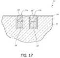
- FIG. 12is a schematic cross-section showing the partially fabricated semiconductor device of FIGS. 10A-11B after recessing and burying the fully silicided gates within their trenches.
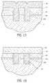
- FIGS. 13-21are a series of cross-sectional views of a portion of a semiconductor device, illustrating simultaneous formation of peripheral transistor gate stacks and recessed access devices (similar to those of FIGS. 1 and 2 ) in the array, according to another embodiment of the invention.
- circuit design of these preferred embodimentsmay be incorporated into any integrated circuit.
- theymay be advantageously applied to form any device having an array of electrical devices, including logic or gate arrays and volatile or non-volatile memory devices, such as DRAMs, RAMs, or flash memory.
- the integrated circuits formed by the methods described hereincan be incorporated in any of a number of larger systems, such as motherboards, desktop or laptop computers, digital cameras, personal digital assistants, or any of a number of devices for which memory is useful.
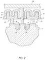
- FIG. 1shows a view of a portion of a memory device 10 .
- This schematic layoutillustrates the various electrical devices and other components that form the memory device 10 .
- the memory device 10is built on and in a substrate 11 , which forms the lowest level of semiconductor material in which electrical devices are formed.
- the substrate 11typically comprises silicon.
- suitable materialse.g., other group III-V elements
- their depth or heightmay be most easily understood with reference to the top surface of the substrate 11 , best seen in FIG. 2 .
- word lines 12 a , 12 b , 12 c , 12 dare also shown in FIG. 1 extending along the memory device 10 .
- these word lines 12were formed using a pitch doubling technique.
- these word lines 12are preferably formed by a method that will be discussed in greater detail with reference to FIGS. 3-9 .
- the pitch of the resulting featuresmay be less than the minimum pitch defined by the photolithographic technique.
- the pitch of the resulting featuresmay equal one half the minimum pitch defined by the photolithographic technique.
- pitch doublingmay be performed by the following sequence of steps, as is well understood by those skilled in the art.
- photolithographymay be used to form a pattern of lines in a photoresist layer overlying a layer of an expendable material and a substrate.
- This photolithographic techniqueachieves a pitch between adjacent lines of 2F, as disclosed above, which pitch is limited by the optical characteristics of photolithography.
- Fis within the range of 60 to 100 nm. This range is typical for state-of-the-art photolithographic techniques used to define features. In one photolithography system, F equals approximately 86 nm, while, in another system, F equals approximately 78 nm.
- each line defined by photolithographyis typically also defined as F, as would be well understood by those skilled in the art.
- the patternmay then be transferred by an etching step (preferably anisotropic) to the lower layer of expendable material, thereby forming placeholders, or mandrels in the lower layer.
- the photoresist linescan then be stripped, and the mandrels can be isotropically etched to increase the distance between neighboring mandrels.
- the distance between the neighboring mandrelsis increased from F to 3F/2.
- the isotropic “shrink” or “trim” etchcould have been performed at the level of the resist.
- a conformal layer of spacer materialmay then be deposited over the mandrels.
- This layer of materialcovers both horizontal and vertical surfaces of the mandrels.
- Spacersi.e., material extending from sidewalls of another material, are therefore formed on the sides of the mandrels by preferentially etching the spacer material from the horizontal surfaces in a directional spacer etch.
- the remaining mandrelsare then selectively removed, leaving behind only the spacers, which together may act as a mask for patterning.
- a given pitch, 2Fformerly included a pattern defining one feature and one space
- the same widthnow includes two features and two spaces defined by the spacers.
- This method of pitch doublingwhich may be repeated for further reduction in the size of the features, will be discussed in greater detail below with reference to FIGS. 3-9 .
- the extent of the shrink/trim etch and the thicknesses of the deposited spacersmay be varied to achieve a variety of feature and pitch sizes.
- the featuresi.e. word lines 12 in the instant example, have a pitch of F.
- the word lines 12are defined by a width of about F/2, and adjacent word lines 12 a , 12 b or 12 c , 12 d are separated by the same width, F/2.
- the separation between the spaced-apart word lines 12 b , 12 cis 3F/2.
- an isolation trenchis filled with an insulator and lies within this separation between these word lines 12 b , 12 c ; however, in other embodiments, this isolation trench need not be present.
- the word linesFor every distance of 3F, there are two word lines, yielding what may be referred to as an effective pitch of 3F/2. More generally, the word lines preferably have an effective pitch between 1.25F and 1.9F. Of course, the particular pitch used to define the word lines is only an example. In other embodiments, the word lines may be fabricated by more conventional techniques, and pitch doubling need not be used. In one embodiment, for example, the word lines may each have a width of F and may be separated by F, 2F, 3F or some other width. In still other embodiments, the word lines need not be formed in pairs either. For example, in one embodiment, only one word line need pass through each active area.
- each word line 12may extend across hundreds, thousands or millions of transistors.
- the word lines 12are typically electrically coupled to a device, such as a power source, that can place a current across the word line 12 .
- the power sources for the word lines 12are indirectly coupled to a CPU through a memory controller.
- the word lines 12comprise a p-type semiconductor, such as silicon doped with boron. In other embodiments, the word lines 12 may comprise an n-type semiconductor, metal silicide, tungsten or other similarly behaving material, as is well-known to those of skill in the art. In some embodiments, the word lines 12 may comprise a variety of materials, in a layered, mixed or chemically bonded configuration.
- the horizontal lines seen in FIG. 1are formed by digit lines 14 a , 14 b .
- the width of each of these digit lines, illustrated as DL in FIG. 1is equal to F.
- No pitch doublinghas been used to form these exemplary digit lines 14 .
- Adjacent digit lines 14 a , 14 bare separated, in a preferred embodiment, by a distance, illustrated as S in FIG. 1 , equal to 2F.
- the pitch of the digit linesis preferably greater than 2.5F, and preferably less than 4F. Without pitch-doubling techniques, the lower limit is, of course, imposed by the photolithographic technique used to form the digit lines.
- the pitch of the digit linesis between 2.75F and 3.25F. This range represents a desirable balance between the ease of manufacturing and the size of the chip.
- the digit lines 14have a pitch of 3F. Of course, in other embodiments, different widths and spacing are possible.
- the entire length of the digit lines 14is also not visible in FIG. 1 , and the digit lines 14 typically extend across many transistors.
- the digit lines 14are typically electrically coupled to current sense amplifiers, and thereby to a power or voltage source.
- the power sources for the digit lines 14are also indirectly coupled to a CPU through a memory controller.
- the sense amplifiersmay be spaced farther from one another, relaxing their manufacturing tolerances, and decreasing the likelihood of capacitance coupling of adjacent digit signals.
- the digit lines 14comprise a conducting metal, such as tungsten, copper, or silver. In other embodiments, other conductors or semiconductors may be used, as is well-known to those of skill in the art.
- the other features visible in FIG. 1are the active areas 16 , illustrated within curvilinear rectangles, which form axes A that are angled relative to the axes B of the digit lines. These rectangles represent a doped region or well within the substrate 11 ; however, in other embodiments, these rectangles need not represent physical structures or materials within or upon the memory device 10 and substrate 11 .
- the active areas 16define those portions of the memory device 10 that contain field effect transistors and are typically surrounded by field isolation elements (e.g., shallow trench isolation (STI)).
- these active areaseach comprise two drains 18 and one source 20 .
- the source and drainsmay be larger or smaller than illustrated in FIG. 1 , as is well known to those of skill in the art. They may also be fabricated in any of a number of ways well-known to those of skill in the art.
- the active areasmay comprise one source and one drain, wherein the source is formed near the digit line, and the drain is separated from the source by a word line.
- the memory devicemay be configured similarly to the memory device 10 in FIG. 1 , but there need only be one word line passing through each active area.
- an active areamay comprise one source and one drain, and the memory device may further comprise two word lines extending near the active area, configured similarly to the paired word lines 12 c , 12 d shown in FIG. 1 .
- the two word linesmay both extend between the source and drain, and provide redundant control of the transistor.
- a digit line 14runs proximal to, and preferably above (see FIG. 2 ), each source 20 that lies in the digit line's row. Meanwhile, each source 20 is separated to either side from its adjacent drains 18 by word lines 12 .
- the source 20 and drains 18comprise an n-type semiconducting material, such as silicon doped with phosphorous or antimony.
- the source 20 and drains 18may comprise a p-type semiconductor, or they may be fabricated from other materials, as is well-known to those of skill in the art. In fact, the source 20 and drains 18 need not be fabricated from the same compounds.
- FIG. 2shows a cross-sectional view of one of the active areas 16 .
- FIG. 2shows a cross-sectional view of one of the active areas 16 .
- the drains 18 and source 20may comprise protrusions from the relatively flat, upper surface of the substrate 11 .
- the source 20 and drains 18are fabricated as one-piece with the substrate 11 , and are raised relative to the surface of the substrate 11 by etching a monolithic wafer or substrate; in another arrangement, the source and drain protrusions are formed by selective epitaxial deposition using techniques well-known to those of skill in the art.
- digit line 14 bis located above the upper surface of source 20 .
- the source 20is electrically coupled to the digit line 14 b by a digit line plug 22 , which plug may be formed in multiple stages or in a single stage, as shown.
- the source 20is separated from the two drains 18 by word lines 12 a , 12 b .
- the word lines 12 a , 12 bare preferably embedded in the substrate 11 , extending downwards from the surface. Transistors of this design are often referred to as recessed access devices or RADs.
- the drains 18are, in turn, electrically coupled to storage capacitors 24 , and, in particular, to the lower electrode 26 of the storage capacitors 24 , by contact plugs 28 .
- the storage capacitors 24comprise a lower electrode 26 separated from a reference electrode 30 by a dielectric material 32 . In this configuration, these stacked storage capacitors 24 function in a manner well known to those of skill in the art. As illustrated, the storage capacitors 24 are preferably located above the plane of the substrate 11 , although trench capacitors can be used in other arrangements.
- every storage capacitor 24forms a reference electrode 30 , while the lower electrode 26 is electrically coupled to an associated drain 18 .
- the word lines 12 a , 12 bfunction as gates in the field effect transistors they pass through, while the digit line 14 b functions as a signal for the sources to which it is electrically coupled.
- the word lines 12 a , 12 bpreferably control access to the storage capacitors 24 coupled to each drain 18 , by allowing or preventing the signal (representing a logic “0” or a logic “1”) carried on the digit line 14 b to be written to or read from the storage capacitors 24 .
- each of the two capacitors 24 connected to an associated drain 18can contain one bit of data (i.e., a logic “0” or logic “1”).
- a logic “0” or logic “1”In a memory array, the combination of the digit line and word line that are selected can uniquely identify the storage capacitor 24 to or from which data should be written or read.
- Axis Arepresents the longitudinal axis of active area 16 .
- the drains 18 and source 20 of each active area 16preferably have a substantially linear relationship that may be used to define a longitudinal axis. As illustrated, all of the active areas 16 are substantially parallel. It will be understood, of course, that the drains 18 and source 20 need not form an absolutely straight line, and indeed a substantial angle may be defined by these three points.
- the axis Amay be defined by the two drains 18 , or by the source 20 and only one of the drains 18 , or in a number of other ways that would be clearly understood by those skilled in the art.
- the axis Amay be defined by a line between the single drain and single source.
- Axis Brepresents the longitudinal axis of digit line 14 b .
- the digit line 14 bforms a substantially straight line.
- the digit lines 14 a , 14 balso preferably form generally parallel axes.
- axis A of every active area 16forms a similar angle with every axis B of the digit lines 14 , at least in the region of each memory cell.
- an acute angleis formed between axis A and axis B.
- this acute angle, ⁇defined between axis A and axis B, is 45°.
- the angling of the active areas 16 relative to the digit lines 14facilitates the location of the contact plugs 28 extending between drains 18 and associated storage capacitors 24 . Since these contact plugs 28 extend from the top surface of the drains 18 in the preferred embodiment (illustrated in FIG. 2 ), the engineering is simplified if the digit lines 14 do not extend over the tops of the drains 18 .
- the distance between a digit line 14 and drains 18may be selected to facilitate electronic contact between the drains and contact plugs, even while the digit line 14 substantially overlaps and contacts the source 20 of the same active area 16 .
- the angle, ⁇may have any of a number of values chosen to maximize the pitch of the electrical devices. As will be readily apparent to one of skill in the art, different angles will yield different pitches between adjacent active areas.
- the angle, ⁇is preferably between 10° and 80° degrees. In a more preferred embodiment, the angle, ⁇ , is between 20° and 60°. In a still more preferred embodiment, the angle, ⁇ , is between 40° and 50°.
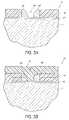
- FIG. 3illustrates a semiconductor substrate 11 over which a thin, temporary layer 40 , comprising oxide in a preferred embodiment, has been formed according to conventional semiconductor processing techniques.
- a hard mask layer 42such as silicon nitride, is then deposited over the substrate 11 and temporary layer 40 .
- the hard mask layer 42may be formed by any well-known deposition process, such as sputtering, chemical vapor deposition (CVD) or low-temperature deposition, among others.
- CVDchemical vapor deposition
- the hard mask layer 42comprises silicon nitride in the preferred embodiment, it must be understood that it may also be formed of silicon oxide, for example, or other materials suitable for the selective etch steps described below.
- the hard mask layer 42is patterned using a photoresist layer formed over the hard mask layer 42 .
- the photoresist layermay be patterned to form a mask using conventional photolithographic techniques, and the hard mask layer 42 may then be anisotropically etched through the patterned photoresist to obtain a plurality of hard mask columns 44 extending in the y-dimension (as defined by FIG. 1 ), with trenches 46 separating those columns.
- the photoresist layermay then be removed by conventional techniques, such as by using an oxygen-based plasma.
- a conformal layer of spacer materialmay be deposited to cover the entire surface of the memory device 10 .
- the spacer materialcan be selectively etched with respect to the substrate 11 and the temporary layer 40 , and the substrate 11 and the temporary layer 40 can each be selectively etched with respect to the spacer material.
- the spacer materialcomprises polysilicon.
- the spacer materialmay be deposited using any suitable deposition process, such as, for example, CVD or physical vapor deposition (PVD).
- an anisotropic etchmay be used to preferentially remove the spacer material from the horizontal surfaces in a directional spacer etch.
- the spacer materialis formed into spacers 48 , i.e., material extending from the sidewalls of another material. As shown in FIG. 5A , spacers 48 are formed within the trench 46 and narrow it.
- a second hard mask layer 49may then be deposited over the entire surface of the memory device 10 .
- This layer of hard mask 49also silicon nitride in a preferred embodiment, is preferably deposited to a thickness sufficient to fill the trench 46 .
- the hard mask material 49may be deposited by any of a number of suitable deposition processes, including CVD or PVD. After deposition of a sufficient amount of hard mask material 49 , the excess that may have formed over the spacers 48 and over the other portions of previously deposited hard mask 42 may be removed by any of a number of processes well-known to those of skill in the art.
- the surface of the device 10may be planarized to the level of the dotted line of FIG. 5B , such that the sidewalls of the remaining spacers 48 are nearly vertical. Any suitable planarization process, such as, for example, chemical mechanical planarization may be used.
- the spacers 48 that are now exposed at the top surface of the memory device 10may be stripped using any of a number of processes.
- a processmay be used that selectively strips polysilicon relative to silicon nitride.
- a selective wet etchmay be used.
- the trenches formed where the spacers 48 have been etchedare further deepened by a secondary etch that selectively etches the temporary layer 40 as well as the substrate 11 .
- These trenchesare also preferably formed using a directional process, such as, for example, ion milling or reactive ion etching.
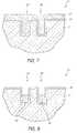
- FIG. 6illustrates the result of these processes, with openings or recesses in the form of trenches 50 separated by less than the minimum pitch possible using photolithographic techniques alone.
- the trenches 50Preferably have a width at top between about 25 nm and 75 nm.
- numerous other techniques for pitch multiplicationmay be used to arrive at the stage shown in FIG. 6 .
- Many such techniqueswill generally include a spacer process, by which physical deposition can achieve a smaller pitch than photolithographic techniques alone.
- the trenches 50typically also have an aspect ratio greater than 1:1, and preferably greater than 2:1. Increased depth maximizes available volume and thence conductivity for the word lines, at the expense of difficulty in filling with a suitable material.
- a gate dielectric layer 54is blanket deposited or thermally grown over the device, lining the inner surfaces of the trenches 50 .
- the illustrated gate dielectric layer 54comprises silicon oxide formed by thermal oxidation in a preferred embodiment, but can also be a deposited high K material in other embodiments.
- a layer of gate material 52which comprises polysilicon in the illustrated embodiment, may then also be blanket deposited over the entire memory device 10 .
- the gate layer 52completely fills the trenches 50 and forms a top surface of the device 10 . In a preferred embodiment, this polysilicon is undoped.
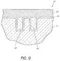
- the undoped polysilicon in the trenches 50is etched back until the top of the gate layer 52 resides beneath the top surface of the substrate 11 . This stage of the process is shown in FIG. 8 .
- the recessed polysilicon 52 of FIG. 8can serve as the word lines and the gate electrodes for the memory cell transistors if appropriately doped.
- the gate electrodes in the arraysare formed of a more highly conductive material than traditional polysilicon gates. This is due to the fact that the recessed gates 12 (see FIGS. 1 and 2 ) are more narrow than the typical gate electrode. Metallic materials compensate, in whole or in part, for the small volume of the gates in the array, improving lateral signal propagation speed along the word lines.
- the undoped polysilicon of FIG. 8can be silicided after recessing by depositing metal thereover and reacting. Metal silicide can have better than 10 times the conductivity of doped polysilicon and demonstrate a suitable work function.
- the polysilicon 52is initially etched back or planarized down to the gate oxide 54 , thus isolating the polysilicon within the trenches 50 without recessing at this stage.
- the polysilicon of the gate layer 52 within the trenches 50is subjected to a salicidation (self-aligned silicidation) reaction to form a layer of conductive material 56 .
- a metal layer 55( FIG. 9 ) may be blanket deposited and an anneal step may form a silicide material 56 ( FIG. 12 ) wherever the metal contacts silicon, such as over the polysilicon gate layers 52 .
- the silicided materialcomprises silicon and one or more metals, such as, for example, tungsten, titanium, ruthenium, tantalum, cobalt or nickel.
- a selective metal etchremoves the excess metal but does not remove the silicide 56 .
- the metal silicide 56thereby forms a self-aligned layer that increases the lateral conductivity along the word line.
- the gate layer 52is fully silicided to maximize lateral conductivity. Full reaction also assures silicide formation down to the bottom of the trenches 50 .
- the channelextends across not only along the bottom of the gate, but also along the gate's sidewalls. Accordingly, incomplete silicidation would result in different work functions along the length of the RAD channel.
- full silicidationensures similar gate work functions across the array, from array to array across a wafer, and from wafer to wafer. It has been found difficult, however, to achieve full silicidation within the tight confines of the illustrated trenches 50 , with a single metal to form the conductive material 56 .
- Other metalshave demonstrated similar difficulties for full silicidation for recessed access devices. The skilled artisan will appreciate that full silicidation can be challenging for material within other types of recesses, such as contact openings or vias, stacked container shapes for capacitors, capacitor trenches, etc.
- the voidingappears to be caused by diffusion during the silicidation reaction, in combination with the tight confines of the high aspect ratio trenches 50 .
- Silicondiffuses more readily in cobalt than cobalt does into silicon. Accordingly, silicon tends to migrate during the reaction, leaving voids in the trenches 50 .
- a high temperature phase transformation annealmay convert the silicide from CoSi to the more stable CoSi 2 .
- Nickeldiffuses more readily into silicon than silicon does into nickel and so also has a tendency to create voids during the reaction in which NiSi is converted into the NiSi 2 phase.
- the metal layer 55preferably comprises a mixture of metals, where at least two of the metals in the mixture have opposing diffusivities relative to silicon.
- the metal layer 55can comprise a mixture of nickel and cobalt, such that the directions of diffusion tend to balance each other and minimize the risk of voiding.
- the cobaltpreferably comprises less than 50 at. % of the mixed metal 55 , and more preferably the mixture comprises about 70-90 at. % Ni and about 10-30 at. % Co.
- Such a mixture of nickel and cobalthas been found to more readily accomplish full silicidation of the gate layer without voiding, thus increasing signal propagation speeds along the word line.
- fully silicided word linesare not only more conductive, but also will ensure consistent work function along the length of the channel. Full silicidation will also demonstrate better consistency from device to device across an array, from array to array, or wafer to wafer, since partial silicidation will tend to leave inconsistent compositions depending upon local temperature variations, etc.
- a sputtering targetcomprising 80% Ni and 20% Co is sputtered over the polysilicon 52 to produce the metal layer 55 .
- the substrateis then subjected to a silicidation anneal. While a high temperature (e.g., 800° C.) anneal is possible for a shorter time, preferably the anneal is conducted at lower temperatures for a longer time. For example, the substrate is annealed at 400-600° C. for 25-35 minutes. In experiments, the silicidation anneal was conducted in a batch furnace under an N 2 environment at 500° C. for 30 minutes.
- metals that diffuse more readily in silicon than silicon does in that metalinclude Ni, Pt and Cu.
- metals in which silicon diffuses more readily than the metal diffuses in siliconinclude Co, Ti and Ta.
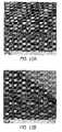
- FIGS. 10A-11Bare micrographs showing recessed, fully silicided Ni x Co y Si z gate material within 50 nm wide trenches lined with silicon oxide.
- FIGS. 10A and 10Bshow cross sections across the width of twin trenches, at two different magnifications.
- FIGS. 11A and 11Bshow cross sections along the length of one of the trenches, at two different magnifications.
- the trencheshave a width at the top of about 50 nm and a depth of about 150 nm, such that the aspect ratio of these trenches was about 3:1.
- a smooth, uniform compositionis observed, filling at least a lower portion of the trenches without voiding.
- FIGS. 11-12after depositing the polysilicon 52 ( FIG. 7 ), the polysilicon can be etched back only to the gate dielectric top surface 54 , thus isolating the silicon within the trenches without recessing.
- the silicided layers 56can be recessed within the trenches and are then covered by a second insulating layer 58 , such as silicon nitride. These insulating layers 58 may be deposited and then etched or planarized.
- the conductive material 56thereby forms the word lines 12 a , 12 b of the completed memory device 10 , and the word lines 12 a , 12 b are separated from the other circuit elements by the insulating layers 58 .
- the word lines 12have been pitch-multiplied, and have a pitch roughly one half of that possible simply using photolithographic techniques. Note, however, that certain aspects of the disclosure herein provide advantages whether or not the word lines are pitch-multiplied.
- the pitch-multiplicationmay take place by any of a variety of processes well-known to those skilled in the art.
- the silicided layers 56 of the illustrated embodimentthus fill lower portions of the trenches 50 , preferably filling greater than 50% of the trench heights, more preferably filling greater than 75% of the trench height.
- about 70-90 at % of metal in the metal silicide 56is nickel and about 10-30 at % of metal in the metal silicide is cobalt.
- the logic in the peripheryis preferably simultaneously defined as certain of the above steps are completed, thereby making the chip-making process more efficient.
- the silicon and metal deposition steps to define recessed word linespreferably simultaneously define gate electrodes over the substrate for the CMOS transistors in the periphery.
- different work functions and resistivitycan be established for the simultaneously processed gate electrodes in the array and the logic regions in the periphery. In the illustrated embodiment, this is facilitated by etching array RAD trenches through a polysilicon layer, which forms part of the gate stack in the periphery.
- a polysilicon layer 60can be deposited over the substrate 11 prior to forming the trenches.
- the polysilicon layer 60can be first deposited over a thin dielectric 54 a (e.g., grown gate oxide).
- the substratecan then be patterned with a pitch-doubled mask (not shown), such as that described with respect to FIGS. 3-6 .
- An etch stop layer 61is also formed, in the illustrated embodiment comprising about 100-200 ⁇ of TEOS-deposited oxide.
- the trenches 50are etched through the overlying etch stop layer 61 , the polysilicon layer 60 , the underlying dielectric 54 a and the substrate 11 .
- the gate dielectric 54 bcan then be formed over the exposed portions of the substrate 11 , such as by oxidation of the trench walls. Due to the pre-existing etch stop layer 61 , no significant further oxide grows over the top surface of the polysilicon 60 , as shown.
- a metallic material 62can be deposited over the polysilicon 60 and into the trenches 50 .
- the trenches 50are preferably filled with material more conductive than polysilicon.
- the metallic material 62comprises titanium nitride (TiN).
- the metallic material 62is preferably etched back or planarized to leave isolated lines of the conductive material 62 in the trenches 50 , stopping on the oxide etch stop layer 61 (see FIG. 15 ).
- the etch stop layer 61 overlying the polysilicon layer 60is removed (e.g., using an HF dip for the preferred oxide material of the etch stop layer 61 ), while the dielectric layer 54 b within the trenches 50 is protected by the metallic material 62 .
- metallic layers 64 , 66are deposited over the silicon layer 60 .
- the first dielectric layer 54 a , the polysilicon layer 60 , and the overlying metallic layers 64 , 66can serve as the transistor gate stack in the periphery. All these layers are deposited in both regions of interest (in the memory example, in both periphery and memory array regions).
- Polysiliconcan be variably doped to establish a desired transistor work function, such that a single material deposition, and different doping steps, can be used to define gates for both NMOS and PMOS of a CMOS circuit.
- the overlying metallic layer 66can serve to improve lateral signal propagation speeds along lines controlling the gates, and comprises tungsten (W) in the illustrated embodiment.
- the intervening metallic layer 64can ensure physical and electrical compatibility (e.g., fulfilling adhesion and barrier functions) at the juncture between the polysilicon layer 60 and the overlying metallic layer 66 , and in the illustrated embodiment comprises titanium nitride, and more particularly metal-rich metal nitride.
- the gate stackalso includes a cap layer 68 , formed of silicon nitride in the illustrated embodiment.
- FIG. 17shows the trenches 50 , filled with the metallic material 62 , in a first or memory array region 70 of the substrate.
- the gate stacks layers 54 a , 60 , 64 , 66 and 68extend across both the array region 70 and the second or periphery or logic region 72 of the substrate.
- a photoresist mask 76is configured for patterning transistor gates in the periphery 72 .
- a series of etch stepsetches first through the cap layer 68 , including a metal etch to remove the metallic layer(s) 64 , 66 .
- Chlorine-based reactive ion etch (RIE)for example, can selectively remove typical metallic materials, such as the illustrated tungsten strapping layer 66 and intervening metal nitride layer 64 , while stopping on the underlying polysilicon layer 60 .
- RIEreactive ion etch
- a high degree of selectivityenables continuing the metal etch after exposure of the polysilicon 60 until the metallic material 62 is recessed in the trenches 50 , as shown.
- the etch chemistrycan be switched following recessing of the metallic gate material 62 in the array trenches, and the silicon 60 can be patterned using the same mask 76 , completing patterning of the gate stacks 80 for the periphery 72 .
- a spacer layer 84is deposited over the substrate, coating the gate stacks 80 conformally but filling the recesses at the top of the array trenches 50 .
- the spacer layer 84comprises silicon nitride, but the skilled artisan will appreciate that a number of different insulating materials can be used.
- a subsequent spacer etchleaves sidewall spacers 86 along sidewalls of the gate stacks 80 , allowing self-aligned doping of source/drain areas.
- the spacer etchmerely etches the spacer material back in the array 72 , leaving an insulating cap layer 88 burying the gate material 62 within the trenches 50 .
- CMOS transistorsincluding source/drain, channel enhancement, gate electrode, lightly doped drain (LDD) and halo doping, are omitted in the description herein for simplicity.
- LDDlightly doped drain
- FIGS. 13-21thus facilitates simultaneous processing of transistors in the array and the periphery.
- the array transistorsare recessed access devices (RADs), whereas the peripheral gates are formed above the substrate 11 as conventional planar MOS transistors. While described in the context of conventional CMOS circuitry in the periphery, the skilled artisan will appreciate that the peripheral transistors can take other forms.
- the metallic layer in the RAD trenchescan be recessed at the same time as patterning the peripheral gate stacks.
- the peripheral sidewall spacersare simultaneously formed with the insulating cap on the RAD gates or word lines.
- DRAM fabrication techniquesmay be used to create the other circuit elements shown in FIG. 2 .
- different levels of dopingmay be used to form the drains 18 and source 20 of FIG. 2
- the stacked storage capacitors 24may be formed according to a plurality of deposition and masking steps.
- the completed memory device 10 shown in FIGS. 1 and 2possesses a number of advantages in comparison to conventional DRAM.
- the size of each memory cell and the overall size of the memory device 10may be substantially reduced without a corresponding, substantial reduction in the distance between adjacent sense amplifiers.
- the word lines 12 and digit lines 14may have substantially different pitches, which enables the digit lines 14 to have far greater separation than the word lines 12 .
- the word lines 12have an effective pitch of 1.5F, while the digit lines 14 may have a pitch of 3F.
- the steps for forming the digit lines 14 and word lines 12are simplified by making them substantially linear and generally perpendicular to one another, while realizing space-savings by placing the active areas 16 at an angle to these elements.
- the word lines 12 in the preferred embodimentare also recessed, and, unlike the layout in conventional DRAM, there is no spacer using up valuable space between the gates and the sources or drains of the active areas (as may be easily seen in FIG. 2 ). Thus, the memory device 10 may be made more dense.
- the use of a mixture of metalsfacilitates full silicidation of the silicon buried within trenches 50 without the harmful formation of voids. Accordingly, a high conductivity can be achieved for the relatively small volume word lines.
Landscapes
- Engineering & Computer Science (AREA)
- Manufacturing & Machinery (AREA)
- Physics & Mathematics (AREA)
- Condensed Matter Physics & Semiconductors (AREA)
- General Physics & Mathematics (AREA)
- Computer Hardware Design (AREA)
- Microelectronics & Electronic Packaging (AREA)
- Power Engineering (AREA)
- Chemical & Material Sciences (AREA)
- Inorganic Chemistry (AREA)
- Semiconductor Memories (AREA)
- Dram (AREA)
Abstract
Description
Claims (31)
Priority Applications (1)
| Application Number | Priority Date | Filing Date | Title |
|---|---|---|---|
| US12/710,082US7935999B2 (en) | 2005-09-01 | 2010-02-22 | Memory device |
Applications Claiming Priority (2)
| Application Number | Priority Date | Filing Date | Title |
|---|---|---|---|
| US11/219,349US7687342B2 (en) | 2005-09-01 | 2005-09-01 | Method of manufacturing a memory device |
| US12/710,082US7935999B2 (en) | 2005-09-01 | 2010-02-22 | Memory device |
Related Parent Applications (1)
| Application Number | Title | Priority Date | Filing Date |
|---|---|---|---|
| US11/219,349DivisionUS7687342B2 (en) | 2005-09-01 | 2005-09-01 | Method of manufacturing a memory device |
Publications (2)
| Publication Number | Publication Date |
|---|---|
| US20100148249A1 US20100148249A1 (en) | 2010-06-17 |
| US7935999B2true US7935999B2 (en) | 2011-05-03 |
Family
ID=37802858
Family Applications (2)
| Application Number | Title | Priority Date | Filing Date |
|---|---|---|---|
| US11/219,349Active2028-05-31US7687342B2 (en) | 2005-09-01 | 2005-09-01 | Method of manufacturing a memory device |
| US12/710,082Expired - LifetimeUS7935999B2 (en) | 2005-09-01 | 2010-02-22 | Memory device |
Family Applications Before (1)
| Application Number | Title | Priority Date | Filing Date |
|---|---|---|---|
| US11/219,349Active2028-05-31US7687342B2 (en) | 2005-09-01 | 2005-09-01 | Method of manufacturing a memory device |
Country Status (8)
| Country | Link |
|---|---|
| US (2) | US7687342B2 (en) |
| EP (1) | EP1929517B1 (en) |
| JP (1) | JP5003979B2 (en) |
| KR (1) | KR101057265B1 (en) |
| CN (1) | CN101297399B (en) |
| SG (1) | SG165334A1 (en) |
| TW (1) | TWI321844B (en) |
| WO (1) | WO2007030346A2 (en) |
Cited By (1)
| Publication number | Priority date | Publication date | Assignee | Title |
|---|---|---|---|---|
| US9064745B2 (en) | 2012-08-29 | 2015-06-23 | International Business Machines Corporation | Sublithographic width finFET employing solid phase epitaxy |
Families Citing this family (89)
| Publication number | Priority date | Publication date | Assignee | Title |
|---|---|---|---|---|
| US7151040B2 (en)* | 2004-08-31 | 2006-12-19 | Micron Technology, Inc. | Methods for increasing photo alignment margins |
| US7910288B2 (en)* | 2004-09-01 | 2011-03-22 | Micron Technology, Inc. | Mask material conversion |
| US7547945B2 (en)* | 2004-09-01 | 2009-06-16 | Micron Technology, Inc. | Transistor devices, transistor structures and semiconductor constructions |
| US7655387B2 (en)* | 2004-09-02 | 2010-02-02 | Micron Technology, Inc. | Method to align mask patterns |
| US7115525B2 (en)* | 2004-09-02 | 2006-10-03 | Micron Technology, Inc. | Method for integrated circuit fabrication using pitch multiplication |
| US7253118B2 (en)* | 2005-03-15 | 2007-08-07 | Micron Technology, Inc. | Pitch reduced patterns relative to photolithography features |
| US7390746B2 (en) | 2005-03-15 | 2008-06-24 | Micron Technology, Inc. | Multiple deposition for integration of spacers in pitch multiplication process |
| US7384849B2 (en) | 2005-03-25 | 2008-06-10 | Micron Technology, Inc. | Methods of forming recessed access devices associated with semiconductor constructions |
| US7611944B2 (en) | 2005-03-28 | 2009-11-03 | Micron Technology, Inc. | Integrated circuit fabrication |
| US7429536B2 (en) | 2005-05-23 | 2008-09-30 | Micron Technology, Inc. | Methods for forming arrays of small, closely spaced features |
| US7560390B2 (en)* | 2005-06-02 | 2009-07-14 | Micron Technology, Inc. | Multiple spacer steps for pitch multiplication |
| US7396781B2 (en)* | 2005-06-09 | 2008-07-08 | Micron Technology, Inc. | Method and apparatus for adjusting feature size and position |
| US7888721B2 (en) | 2005-07-06 | 2011-02-15 | Micron Technology, Inc. | Surround gate access transistors with grown ultra-thin bodies |
| US7282401B2 (en) | 2005-07-08 | 2007-10-16 | Micron Technology, Inc. | Method and apparatus for a self-aligned recessed access device (RAD) transistor gate |
| US7768051B2 (en) | 2005-07-25 | 2010-08-03 | Micron Technology, Inc. | DRAM including a vertical surround gate transistor |
| US7413981B2 (en) | 2005-07-29 | 2008-08-19 | Micron Technology, Inc. | Pitch doubled circuit layout |
| US8123968B2 (en)* | 2005-08-25 | 2012-02-28 | Round Rock Research, Llc | Multiple deposition for integration of spacers in pitch multiplication process |
| US7816262B2 (en) | 2005-08-30 | 2010-10-19 | Micron Technology, Inc. | Method and algorithm for random half pitched interconnect layout with constant spacing |
| US7867851B2 (en) | 2005-08-30 | 2011-01-11 | Micron Technology, Inc. | Methods of forming field effect transistors on substrates |
| US7829262B2 (en)* | 2005-08-31 | 2010-11-09 | Micron Technology, Inc. | Method of forming pitch multipled contacts |
| US7696567B2 (en) | 2005-08-31 | 2010-04-13 | Micron Technology, Inc | Semiconductor memory device |
| US7776744B2 (en)* | 2005-09-01 | 2010-08-17 | Micron Technology, Inc. | Pitch multiplication spacers and methods of forming the same |
| US7687342B2 (en)* | 2005-09-01 | 2010-03-30 | Micron Technology, Inc. | Method of manufacturing a memory device |
| US7572572B2 (en)* | 2005-09-01 | 2009-08-11 | Micron Technology, Inc. | Methods for forming arrays of small, closely spaced features |
| US7393789B2 (en)* | 2005-09-01 | 2008-07-01 | Micron Technology, Inc. | Protective coating for planarization |
| US7416943B2 (en)* | 2005-09-01 | 2008-08-26 | Micron Technology, Inc. | Peripheral gate stacks and recessed array gates |
| US7557032B2 (en)* | 2005-09-01 | 2009-07-07 | Micron Technology, Inc. | Silicided recessed silicon |
| US7759197B2 (en)* | 2005-09-01 | 2010-07-20 | Micron Technology, Inc. | Method of forming isolated features using pitch multiplication |
| US7700441B2 (en)* | 2006-02-02 | 2010-04-20 | Micron Technology, Inc. | Methods of forming field effect transistors, methods of forming field effect transistor gates, methods of forming integrated circuitry comprising a transistor gate array and circuitry peripheral to the gate array, and methods of forming integrated circuitry comprising a transistor gate array including first gates and second grounded isolation gates |
| US7476933B2 (en) | 2006-03-02 | 2009-01-13 | Micron Technology, Inc. | Vertical gated access transistor |
| US7842558B2 (en)* | 2006-03-02 | 2010-11-30 | Micron Technology, Inc. | Masking process for simultaneously patterning separate regions |
| WO2007113878A1 (en)* | 2006-04-06 | 2007-10-11 | Stmicroelectronics S.R.L. | Process for manufacturing an interaction structure for a storage medium |
| US7902074B2 (en) | 2006-04-07 | 2011-03-08 | Micron Technology, Inc. | Simplified pitch doubling process flow |
| US8003310B2 (en)* | 2006-04-24 | 2011-08-23 | Micron Technology, Inc. | Masking techniques and templates for dense semiconductor fabrication |
| US7488685B2 (en) | 2006-04-25 | 2009-02-10 | Micron Technology, Inc. | Process for improving critical dimension uniformity of integrated circuit arrays |
| US7795149B2 (en) | 2006-06-01 | 2010-09-14 | Micron Technology, Inc. | Masking techniques and contact imprint reticles for dense semiconductor fabrication |
| US7723009B2 (en) | 2006-06-02 | 2010-05-25 | Micron Technology, Inc. | Topography based patterning |
| US8852851B2 (en) | 2006-07-10 | 2014-10-07 | Micron Technology, Inc. | Pitch reduction technology using alternating spacer depositions during the formation of a semiconductor device and systems including same |
| US7602001B2 (en) | 2006-07-17 | 2009-10-13 | Micron Technology, Inc. | Capacitorless one transistor DRAM cell, integrated circuitry comprising an array of capacitorless one transistor DRAM cells, and method of forming lines of capacitorless one transistor DRAM cells |
| US7772632B2 (en)* | 2006-08-21 | 2010-08-10 | Micron Technology, Inc. | Memory arrays and methods of fabricating memory arrays |
| US7611980B2 (en) | 2006-08-30 | 2009-11-03 | Micron Technology, Inc. | Single spacer process for multiplying pitch by a factor greater than two and related intermediate IC structures |
| US7589995B2 (en)* | 2006-09-07 | 2009-09-15 | Micron Technology, Inc. | One-transistor memory cell with bias gate |
| US7858471B2 (en) | 2006-09-13 | 2010-12-28 | Micron Technology, Inc. | Methods of fabricating an access transistor for an integrated circuit device, methods of fabricating periphery transistors and access transistors, and methods of fabricating an access device comprising access transistors in an access circuitry region and peripheral transistors in a peripheral circuitry region spaced from the access circuitry region |
| US7666578B2 (en)* | 2006-09-14 | 2010-02-23 | Micron Technology, Inc. | Efficient pitch multiplication process |
| US8129289B2 (en) | 2006-10-05 | 2012-03-06 | Micron Technology, Inc. | Method to deposit conformal low temperature SiO2 |
| US7642572B2 (en)* | 2007-04-13 | 2010-01-05 | Qimonda Ag | Integrated circuit having a memory cell array and method of forming an integrated circuit |
| US20080296674A1 (en)* | 2007-05-30 | 2008-12-04 | Qimonda Ag | Transistor, integrated circuit and method of forming an integrated circuit |
| US7923373B2 (en)* | 2007-06-04 | 2011-04-12 | Micron Technology, Inc. | Pitch multiplication using self-assembling materials |
| US8980756B2 (en) | 2007-07-30 | 2015-03-17 | Micron Technology, Inc. | Methods for device fabrication using pitch reduction |
| US8563229B2 (en)* | 2007-07-31 | 2013-10-22 | Micron Technology, Inc. | Process of semiconductor fabrication with mask overlay on pitch multiplied features and associated structures |
| DE102008064930B3 (en)* | 2007-09-18 | 2022-09-15 | Samsung Electronics Co., Ltd. | Reduced thickness semiconductor device |
| US8120123B2 (en)* | 2007-09-18 | 2012-02-21 | Samsung Electronics Co., Ltd. | Semiconductor device and method of forming the same |
| US7737039B2 (en) | 2007-11-01 | 2010-06-15 | Micron Technology, Inc. | Spacer process for on pitch contacts and related structures |
| US7659208B2 (en) | 2007-12-06 | 2010-02-09 | Micron Technology, Inc | Method for forming high density patterns |
| US7790531B2 (en) | 2007-12-18 | 2010-09-07 | Micron Technology, Inc. | Methods for isolating portions of a loop of pitch-multiplied material and related structures |
| US8030218B2 (en) | 2008-03-21 | 2011-10-04 | Micron Technology, Inc. | Method for selectively modifying spacing between pitch multiplied structures |
| US7989307B2 (en) | 2008-05-05 | 2011-08-02 | Micron Technology, Inc. | Methods of forming isolated active areas, trenches, and conductive lines in semiconductor structures and semiconductor structures including the same |
| US10151981B2 (en) | 2008-05-22 | 2018-12-11 | Micron Technology, Inc. | Methods of forming structures supported by semiconductor substrates |
| US8076208B2 (en) | 2008-07-03 | 2011-12-13 | Micron Technology, Inc. | Method for forming transistor with high breakdown voltage using pitch multiplication technique |
| US8169031B2 (en) | 2008-08-26 | 2012-05-01 | International Business Machines Corporation | Continuous metal semiconductor alloy via for interconnects |
| US8101497B2 (en)* | 2008-09-11 | 2012-01-24 | Micron Technology, Inc. | Self-aligned trench formation |
| JP2010080514A (en)* | 2008-09-24 | 2010-04-08 | Toshiba Corp | Semiconductor storage device |
| US8492282B2 (en)* | 2008-11-24 | 2013-07-23 | Micron Technology, Inc. | Methods of forming a masking pattern for integrated circuits |
| US8273634B2 (en)* | 2008-12-04 | 2012-09-25 | Micron Technology, Inc. | Methods of fabricating substrates |
| US8247302B2 (en) | 2008-12-04 | 2012-08-21 | Micron Technology, Inc. | Methods of fabricating substrates |
| US8796155B2 (en) | 2008-12-04 | 2014-08-05 | Micron Technology, Inc. | Methods of fabricating substrates |
| US8268543B2 (en)* | 2009-03-23 | 2012-09-18 | Micron Technology, Inc. | Methods of forming patterns on substrates |
| KR101159900B1 (en)* | 2009-04-22 | 2012-06-25 | 에스케이하이닉스 주식회사 | Semiconductor device and method of fabricating the same |
| US9330934B2 (en)* | 2009-05-18 | 2016-05-03 | Micron Technology, Inc. | Methods of forming patterns on substrates |
| KR101623123B1 (en)* | 2009-07-23 | 2016-05-23 | 삼성전자주식회사 | Semiconductor device and method of fabricating the same |
| US20110129991A1 (en)* | 2009-12-02 | 2011-06-02 | Kyle Armstrong | Methods Of Patterning Materials, And Methods Of Forming Memory Cells |
| US8470654B2 (en)* | 2010-02-23 | 2013-06-25 | Micron Technology, Inc. | Methods of forming an electrically conductive buried line and an electrical contact thereto and methods of forming a buried access line and an electrical contact thereto |
| US8518788B2 (en) | 2010-08-11 | 2013-08-27 | Micron Technology, Inc. | Methods of forming a plurality of capacitors |
| US8455341B2 (en) | 2010-09-02 | 2013-06-04 | Micron Technology, Inc. | Methods of forming features of integrated circuitry |
| US8575032B2 (en) | 2011-05-05 | 2013-11-05 | Micron Technology, Inc. | Methods of forming a pattern on a substrate |
| US8877593B2 (en) | 2011-07-31 | 2014-11-04 | International Business Machines Corporation | Semiconductor device including an asymmetric feature, and method of making the same |
| US9076680B2 (en) | 2011-10-18 | 2015-07-07 | Micron Technology, Inc. | Integrated circuitry, methods of forming capacitors, and methods of forming integrated circuitry comprising an array of capacitors and circuitry peripheral to the array |
| US9177794B2 (en) | 2012-01-13 | 2015-11-03 | Micron Technology, Inc. | Methods of patterning substrates |
| US8629048B1 (en) | 2012-07-06 | 2014-01-14 | Micron Technology, Inc. | Methods of forming a pattern on a substrate |
| US9984191B2 (en) | 2014-08-29 | 2018-05-29 | Taiwan Semiconductor Manufacturing Company | Cell layout and structure |
| JP2016072536A (en) | 2014-09-30 | 2016-05-09 | 株式会社東芝 | Storage device |
| US9171847B1 (en)* | 2014-10-02 | 2015-10-27 | Inotera Memories, Inc. | Semiconductor structure |
| US9379197B1 (en)* | 2015-10-07 | 2016-06-28 | Inotera Memories, Inc. | Recess array device |
| CN106783743B (en)* | 2015-11-23 | 2019-07-26 | 华邦电子股份有限公司 | Memory device and its manufacturing method |
| TWI697032B (en)* | 2016-10-24 | 2020-06-21 | 聯華電子股份有限公司 | Method of fabricating semiconductor device |
| US9858995B1 (en)* | 2016-12-22 | 2018-01-02 | Macronix International Co., Ltd. | Method for operating a memory device |
| US9935114B1 (en)* | 2017-01-10 | 2018-04-03 | Micron Technology, Inc. | Methods of forming an array comprising pairs of vertically opposed capacitors and arrays comprising pairs of vertically opposed capacitors |
| CN109427787A (en)* | 2017-08-30 | 2019-03-05 | 联华电子股份有限公司 | Semiconductor memory device with a plurality of memory cells |
| KR102863624B1 (en) | 2021-02-19 | 2025-09-22 | 삼성전자주식회사 | Semiconductor device |
Citations (272)
| Publication number | Priority date | Publication date | Assignee | Title |
|---|---|---|---|---|
| US3731287A (en) | 1971-07-02 | 1973-05-01 | Gen Instrument Corp | Single device memory system having shift register output characteristics |
| US3732287A (en) | 1969-09-09 | 1973-05-08 | Basf Ag | Bismonocarboxylic esters of 3-formylbutanediol-1,2 |
| US4234362A (en) | 1978-11-03 | 1980-11-18 | International Business Machines Corporation | Method for forming an insulator between layers of conductive material |
| US4419809A (en) | 1981-12-30 | 1983-12-13 | International Business Machines Corporation | Fabrication process of sub-micrometer channel length MOSFETs |
| US4432132A (en) | 1981-12-07 | 1984-02-21 | Bell Telephone Laboratories, Incorporated | Formation of sidewall oxide layers by reactive oxygen ion etching to define submicron features |
| US4502914A (en) | 1982-11-13 | 1985-03-05 | International Business Machines Corporation | Method of making structures with dimensions in the sub-micrometer range |
| US4508579A (en) | 1981-03-30 | 1985-04-02 | International Business Machines Corporation | Lateral device structures using self-aligned fabrication techniques |
| US4570325A (en) | 1983-12-16 | 1986-02-18 | Kabushiki Kaisha Toshiba | Manufacturing a field oxide region for a semiconductor device |
| US4648937A (en) | 1985-10-30 | 1987-03-10 | International Business Machines Corporation | Method of preventing asymmetric etching of lines in sub-micrometer range sidewall images transfer |
| EP0227303A2 (en) | 1985-11-25 | 1987-07-01 | Plessey Overseas Limited | Method of manufacturing semiconductor devices having side-wall isolation |
| US4716131A (en) | 1983-11-28 | 1987-12-29 | Nec Corporation | Method of manufacturing semiconductor device having polycrystalline silicon layer with metal silicide film |
| US4776922A (en) | 1987-10-30 | 1988-10-11 | International Business Machines Corporation | Formation of variable-width sidewall structures |
| US4838991A (en) | 1987-10-30 | 1989-06-13 | International Business Machines Corporation | Process for defining organic sidewall structures |
| US4903344A (en) | 1987-07-07 | 1990-02-20 | Oki Electric Industry Co., Ltd. | Semiconductor memory device with staggered sense amplifiers |
| US4983544A (en) | 1986-10-20 | 1991-01-08 | International Business Machines Corporation | Silicide bridge contact process |
| US5013680A (en) | 1990-07-18 | 1991-05-07 | Micron Technology, Inc. | Process for fabricating a DRAM array having feature widths that transcend the resolution limit of available photolithography |
| US5024959A (en) | 1989-09-25 | 1991-06-18 | Motorola, Inc. | CMOS process using doped glass layer |
| US5047117A (en) | 1990-09-26 | 1991-09-10 | Micron Technology, Inc. | Method of forming a narrow self-aligned, annular opening in a masking layer |
| US5053105A (en) | 1990-07-19 | 1991-10-01 | Micron Technology, Inc. | Process for creating an etch mask suitable for deep plasma etches employing self-aligned silicidation of a metal layer masked with a silicon dioxide template |
| US5064683A (en) | 1990-10-29 | 1991-11-12 | Motorola, Inc. | Method for polish planarizing a semiconductor substrate by using a boron nitride polish stop |
| US5117027A (en) | 1990-10-31 | 1992-05-26 | Huls Aktiengesellschaft | Process for the preparation of organosilanes containing methacryloyloxy or acryloyloxy groups |
| US5122848A (en) | 1991-04-08 | 1992-06-16 | Micron Technology, Inc. | Insulated-gate vertical field-effect transistor with high current drive and minimum overlap capacitance |
| EP0491408A2 (en) | 1990-11-20 | 1992-06-24 | Consorzio per la Ricerca sulla Microelettronica nel Mezzogiorno - CoRiMMe | Process for making planarized sub-micrometric trenches in integrated circuits |
| US5177027A (en) | 1990-08-17 | 1993-01-05 | Micron Technology, Inc. | Process for fabricating, on the edge of a silicon mesa, a MOSFET which has a spacer-shaped gate and a right-angled channel path |
| US5250450A (en) | 1991-04-08 | 1993-10-05 | Micron Technology, Inc. | Insulated-gate vertical field-effect transistor with high current drive and minimum overlap capacitance |
| US5295092A (en) | 1992-01-21 | 1994-03-15 | Sharp Kabushiki Kaisha | Semiconductor read only memory |
| US5305252A (en) | 1990-07-06 | 1994-04-19 | Nec Corporation | Semiconductor memory device having memory cell matrix obliquely arranged with respect to bit lines |
| DE4236609A1 (en) | 1992-10-29 | 1994-05-05 | Siemens Ag | Method for forming a structure in the surface of a substrate - with an auxiliary structure laterally bounding an initial masking structure, followed by selective removal of masking structure using the auxiliary structure as an etching mask |
| US5328810A (en) | 1990-05-07 | 1994-07-12 | Micron Technology, Inc. | Method for reducing, by a factor or 2-N, the minimum masking pitch of a photolithographic process |
| US5330879A (en) | 1992-07-16 | 1994-07-19 | Micron Technology, Inc. | Method for fabrication of close-tolerance lines and sharp emission tips on a semiconductor wafer |
| US5391901A (en) | 1992-10-30 | 1995-02-21 | Nec Corporation | Semiconductor memory with oblique folded bit-line arrangement |
| US5495441A (en) | 1994-05-18 | 1996-02-27 | United Microelectronics Corporation | Split-gate flash memory cell |
| US5514885A (en) | 1986-10-09 | 1996-05-07 | Myrick; James J. | SOI methods and apparatus |
| US5539229A (en) | 1994-12-28 | 1996-07-23 | International Business Machines Corporation | MOSFET with raised STI isolation self-aligned to the gate stack |
| US5569620A (en) | 1992-09-03 | 1996-10-29 | Harris Corporation | Bonded wafer processing with metal silicidation |
| US5596759A (en) | 1989-11-03 | 1997-01-21 | Compaq Computer Corporation | Method for initializing a multiple processor computer system using a common ROM |
| US5604159A (en) | 1994-01-31 | 1997-02-18 | Motorola, Inc. | Method of making a contact structure |
| US5638318A (en) | 1995-09-11 | 1997-06-10 | Micron Technology, Inc. | Ferroelectric memory using ferroelectric reference cells |
| US5645887A (en) | 1994-01-14 | 1997-07-08 | Lg Semicon Co., Ltd. | Method for forming platinum silicide plugs |
| US5670794A (en) | 1994-10-07 | 1997-09-23 | Micron Technology, Inc. | Thin film transistors |
| US5677865A (en) | 1995-09-11 | 1997-10-14 | Micron Technology, Inc. | Ferroelectric memory using reference charge circuit |
| US5680344A (en) | 1995-09-11 | 1997-10-21 | Micron Technology, Inc. | Circuit and method of operating a ferrolectric memory in a DRAM mode |
| US5700733A (en) | 1995-06-27 | 1997-12-23 | Micron Technology, Inc. | Semiconductor processing methods of forming field oxide regions on a semiconductor substrate |
| US5748519A (en) | 1996-12-13 | 1998-05-05 | Motorola, Inc. | Method of selecting a memory cell in a magnetic random access memory device |
| US5753546A (en) | 1995-06-30 | 1998-05-19 | Hyundai Electronics Industries Co., Ltd. | Method for fabricating metal oxide field effect transistors |
| US5756395A (en) | 1995-08-18 | 1998-05-26 | Lsi Logic Corporation | Process for forming metal interconnect structures for use with integrated circuit devices to form integrated circuit structures |
| US5780349A (en) | 1997-02-20 | 1998-07-14 | National Semiconductor Corporation | Self-aligned MOSFET gate/source/drain salicide formation |
| US5789320A (en) | 1996-04-23 | 1998-08-04 | International Business Machines Corporation | Plating of noble metal electrodes for DRAM and FRAM |
| US5789269A (en) | 1995-07-11 | 1998-08-04 | Advanced Micro Devices, Inc. | Field implant for semiconductor device |
| US5795830A (en) | 1995-06-06 | 1998-08-18 | International Business Machines Corporation | Reducing pitch with continuously adjustable line and space dimensions |
| US5798544A (en) | 1994-04-22 | 1998-08-25 | Nec Corporation | Semiconductor memory device having trench isolation regions and bit lines formed thereover |
| US5804458A (en) | 1996-12-16 | 1998-09-08 | Motorola, Inc. | Method of fabricating spaced apart submicron magnetic memory cells |
| US5841611A (en) | 1994-05-02 | 1998-11-24 | Matsushita Electric Industrial Co., Ltd. | Magnetoresistance effect device and magnetoresistance effect type head, memory device, and amplifying device using the same |
| US5861328A (en) | 1996-10-07 | 1999-01-19 | Motorola, Inc. | Method of fabricating GMR devices |
| US5892708A (en) | 1992-09-24 | 1999-04-06 | Nonvolatile Electronics, Incorporated | Magnetoresistive memory using large fraction of memory cell films for data storage |
| US5895238A (en) | 1996-12-12 | 1999-04-20 | Nec Corporation | Doping technique for MOS devices |
| US5902690A (en) | 1997-02-25 | 1999-05-11 | Motorola, Inc. | Stray magnetic shielding for a non-volatile MRAM |
| US5909618A (en) | 1997-07-08 | 1999-06-01 | Micron Technology, Inc. | Method of making memory cell with vertical transistor and buried word and body lines |
| US5913116A (en) | 1997-01-08 | 1999-06-15 | Advanced Micro Devices | Method of manufacturing an active region of a semiconductor by diffusing a dopant out of a sidewall spacer |
| US5917749A (en) | 1997-05-23 | 1999-06-29 | Motorola, Inc. | MRAM cell requiring low switching field |
| US5949101A (en) | 1994-08-31 | 1999-09-07 | Kabushiki Kaisha Toshiba | Semiconductor memory device comprising multi-level logic value of the threshold voltage |
| US5956267A (en) | 1997-12-18 | 1999-09-21 | Honeywell Inc | Self-aligned wordline keeper and method of manufacture therefor |
| US5963803A (en) | 1998-02-02 | 1999-10-05 | Advanced Micro Devices, Inc. | Method of making N-channel and P-channel IGFETs with different gate thicknesses and spacer widths |
| US5963469A (en) | 1998-02-24 | 1999-10-05 | Micron Technology, Inc. | Vertical bipolar read access for low voltage memory cell |
| US5977579A (en) | 1998-12-03 | 1999-11-02 | Micron Technology, Inc. | Trench dram cell with vertical device and buried word lines |
| US5994743A (en) | 1997-02-06 | 1999-11-30 | Nec Corporation | Semiconductor device having different sidewall widths and different source/drain depths for NMOS & PMOS structures |
| US5998256A (en) | 1996-11-01 | 1999-12-07 | Micron Technology, Inc. | Semiconductor processing methods of forming devices on a substrate, forming device arrays on a substrate, forming conductive lines on a substrate, and forming capacitor arrays on a substrate, and integrated circuitry |
| US6005800A (en) | 1998-11-23 | 1999-12-21 | International Business Machines Corporation | Magnetic memory array with paired asymmetric memory cells for improved write margin |
| US6004862A (en) | 1998-01-20 | 1999-12-21 | Advanced Micro Devices, Inc. | Core array and periphery isolation technique |
| US6010946A (en) | 1996-08-21 | 2000-01-04 | Nec Corporation | Semiconductor device with isolation insulating film tapered and method of manufacturing the same |
| US6042998A (en) | 1993-09-30 | 2000-03-28 | The University Of New Mexico | Method and apparatus for extending spatial frequencies in photolithography images |
| US6057573A (en) | 1998-05-27 | 2000-05-02 | Vanguard International Semiconductor Corporation | Design for high density memory with relaxed metal pitch |
| US6063688A (en) | 1997-09-29 | 2000-05-16 | Intel Corporation | Fabrication of deep submicron structures and quantum wire transistors using hard-mask transistor width definition |
| US6066191A (en) | 1997-05-21 | 2000-05-23 | Kabushiki Kaisha Toyota Chuo Kenkyusho | Hard molybdenum alloy, wear resistant alloy and method for manufacturing the same |
| US6071789A (en) | 1998-11-10 | 2000-06-06 | Vanguard International Semiconductor Corporation | Method for simultaneously fabricating a DRAM capacitor and metal interconnections |
| US6097065A (en) | 1998-03-30 | 2000-08-01 | Micron Technology, Inc. | Circuits and methods for dual-gated transistors |
| US6104068A (en) | 1998-09-01 | 2000-08-15 | Micron Technology, Inc. | Structure and method for improved signal processing |
| US6104633A (en) | 1998-02-10 | 2000-08-15 | International Business Machines Corporation | Intentional asymmetry imposed during fabrication and/or access of magnetic tunnel junction devices |
| US6134139A (en) | 1999-07-28 | 2000-10-17 | Hewlett-Packard | Magnetic memory structure with improved half-select margin |
| US6141204A (en) | 1996-01-03 | 2000-10-31 | Micron Technology, Inc. | Capacitor constructions and semiconductor processing method of forming capacitor constructions |
| US6147405A (en) | 1998-02-19 | 2000-11-14 | Micron Technology, Inc. | Asymmetric, double-sided self-aligned silicide and method of forming the same |
| US6150211A (en) | 1996-12-11 | 2000-11-21 | Micron Technology, Inc. | Methods of forming storage capacitors in integrated circuitry memory cells and integrated circuitry |
| US6150687A (en) | 1997-07-08 | 2000-11-21 | Micron Technology, Inc. | Memory cell having a vertical transistor with buried source/drain and dual gates |
| US6157064A (en) | 1997-12-15 | 2000-12-05 | Taiwan Semiconductor Manufacturing Company Ltd. | Method and a deep sub-micron field effect transistor structure for suppressing short channel effects |
| US6165833A (en) | 1997-12-19 | 2000-12-26 | Micron Technology, Inc. | Semiconductor processing method of forming a capacitor |
| US6175146B1 (en) | 1997-03-13 | 2001-01-16 | Micron Technology, Inc. | Semiconductor processing methods of forming integrated circuitry memory devices, methods of forming capacitor containers, methods of making electrical connection to circuit nodes and related integrated circuitry |
| US6191470B1 (en) | 1997-07-08 | 2001-02-20 | Micron Technology, Inc. | Semiconductor-on-insulator memory cell with buried word and body lines |
| US6211044B1 (en) | 1999-04-12 | 2001-04-03 | Advanced Micro Devices | Process for fabricating a semiconductor device component using a selective silicidation reaction |
| US6236590B1 (en) | 2000-07-21 | 2001-05-22 | Hewlett-Packard Company | Optimal write conductors layout for improved performance in MRAM |
| US20010005631A1 (en) | 1999-12-14 | 2001-06-28 | Jin-Won Kim | Method for manufacturing an electrode of a capacitor |
| US6271080B1 (en) | 1999-12-16 | 2001-08-07 | International Business Machines Corporation | Structure and method for planar MOSFET DRAM cell free of wordline gate conductor to storage trench overlay sensitivity |
| US6274905B1 (en) | 1999-06-30 | 2001-08-14 | Fairchild Semiconductor Corporation | Trench structure substantially filled with high-conductivity material |
| US6282113B1 (en) | 1999-09-29 | 2001-08-28 | International Business Machines Corporation | Four F-squared gapless dual layer bitline DRAM array architecture |
| US20010019870A1 (en) | 1997-04-25 | 2001-09-06 | Noble Wendell P. | Semiconductor processing methods of forming integrated circuitry, forming conductive lines, forming a conductive grid, forming a conductive network, forming an electrical interconnection to a node location forming an electrical interconnection with a transistor source/drain region, and integrated circuitry |
| US6288454B1 (en) | 1999-05-13 | 2001-09-11 | Lsi Logic Corporation | Semiconductor wafer having a layer-to-layer alignment mark and method for fabricating the same |
| US6291334B1 (en) | 1997-12-19 | 2001-09-18 | Applied Materials, Inc. | Etch stop layer for dual damascene process |
| EP1061592A3 (en) | 1999-06-17 | 2001-09-26 | Matsushita Electric Industrial Co., Ltd. | Magneto-resistance effect element, and its use as memory element |
| US6297554B1 (en) | 2000-03-10 | 2001-10-02 | United Microelectronics Corp. | Dual damascene interconnect structure with reduced parasitic capacitance |
| US6320222B1 (en) | 1998-09-01 | 2001-11-20 | Micron Technology, Inc. | Structure and method for reducing threshold voltage variations due to dopant fluctuations |
| US20020000608A1 (en) | 2000-06-02 | 2002-01-03 | Hirofumi Harada | Vertical MOS transistor and a method of manufacturing the same |
| US6348380B1 (en) | 2000-08-25 | 2002-02-19 | Micron Technology, Inc. | Use of dilute steam ambient for improvement of flash devices |
| US20020024081A1 (en) | 2000-08-27 | 2002-02-28 | Achim Gratz | Vertical non-volatile semiconductor memory cell and method for manufaturing the memory cell |
| US6362057B1 (en) | 1999-10-26 | 2002-03-26 | Motorola, Inc. | Method for forming a semiconductor device |
| US6368950B1 (en) | 2000-12-12 | 2002-04-09 | Advanced Micro Devices, Inc. | Silicide gate transistors |
| US20020042198A1 (en) | 2000-09-20 | 2002-04-11 | Bjarni Bjarnason | Method in etching of a substrate |
| US20020045308A1 (en) | 1996-11-01 | 2002-04-18 | Werner Juengling | Semiconductor processing methods of forming a plurality of capacitors on a substrate, bit line contacts and method of forming bit line contacts |
| US6377070B1 (en) | 2001-02-09 | 2002-04-23 | Micron Technology, Inc. | In-service programmable logic arrays with ultra thin vertical body transistors |
| US6383907B1 (en) | 1999-09-08 | 2002-05-07 | Sony Corporation | Process for fabricating a semiconductor device |
| US6396096B1 (en) | 2000-06-21 | 2002-05-28 | International Business Machines Corporation | Design layout for a dense memory cell structure |
| US20020063110A1 (en) | 2000-11-30 | 2002-05-30 | Cantell Marc W. | Etching of hard masks |
| US6404056B1 (en) | 1994-01-20 | 2002-06-11 | Mitsubishi Denki Kabushiki Kaisha | Semiconductor integrated circuit |
| US6424561B1 (en) | 2000-07-18 | 2002-07-23 | Micron Technology, Inc. | MRAM architecture using offset bits for increased write selectivity |
| US6423474B1 (en) | 2000-03-21 | 2002-07-23 | Micron Technology, Inc. | Use of DARC and BARC in flash memory processing |
| US6424001B1 (en) | 2001-02-09 | 2002-07-23 | Micron Technology, Inc. | Flash memory with ultra thin vertical body transistors |
| US20020102848A1 (en) | 2000-12-07 | 2002-08-01 | Advanced Micro Devices, Inc. | Damascene nisi metal gate high-k transistor |
| US20020123216A1 (en) | 2001-03-05 | 2002-09-05 | Natsuki Yokoyama | Method of manufacturing semiconductor device |
| US6448601B1 (en) | 2001-02-09 | 2002-09-10 | Micron Technology, Inc. | Memory address and decode circuits with ultra thin body transistors |
| US20020130348A1 (en) | 2001-03-16 | 2002-09-19 | Tran Luan C. | 6F2 dram array, a dram array formed on a semiconductive substrate, a method of forming memory cells in a 6F2 dram array and a method of isolating a single row of memory cells in a 6F2 dram array |
| US6455372B1 (en) | 2000-08-14 | 2002-09-24 | Micron Technology, Inc. | Nucleation for improved flash erase characteristics |
| US6465309B1 (en) | 2000-12-12 | 2002-10-15 | Advanced Micro Devices, Inc. | Silicide gate transistors |
| US20020158273A1 (en) | 2000-10-17 | 2002-10-31 | Hitachi, Ltd. | Nonvolatile semiconductor memory device and a method of manufacturing the same |
| US20020160557A1 (en) | 2001-04-28 | 2002-10-31 | Koninklijke Philips Electronics N.V. | Trench-gate semiconductor devices and their manufacture |
| US6475897B1 (en) | 1999-11-10 | 2002-11-05 | Seiko Instruments Inc. | Semiconductor device and method of forming semiconductor device |
| US20020182871A1 (en) | 2001-05-31 | 2002-12-05 | Zhijian Lu | Method for removing polysilane from a semiconductor without stripping |
| US20020187578A1 (en) | 2001-06-12 | 2002-12-12 | Kwon Hong | Method for manufacturing memory device |
| US6496034B2 (en) | 2001-02-09 | 2002-12-17 | Micron Technology, Inc. | Programmable logic arrays with ultra thin body transistors |
| US6498062B2 (en) | 2001-04-27 | 2002-12-24 | Micron Technology, Inc. | DRAM access transistor |
| US20030006410A1 (en) | 2000-03-01 | 2003-01-09 | Brian Doyle | Quantum wire gate device and method of making same |
| US6514884B2 (en) | 1998-02-06 | 2003-02-04 | Semiconductor Process Laboratory Co., Ltd. | Method for reforming base surface, method for manufacturing semiconductor device and equipment for manufacturing the same |
| US6522584B1 (en) | 2001-08-02 | 2003-02-18 | Micron Technology, Inc. | Programming methods for multi-level flash EEPROMs |
| US20030044722A1 (en) | 2001-08-28 | 2003-03-06 | Yi-Yu Hsu | Process for improving critical dimension uniformity |
| US6531727B2 (en) | 2001-02-09 | 2003-03-11 | Micron Technology, Inc. | Open bit line DRAM with ultra thin body transistors |
| US6534243B1 (en) | 2000-10-23 | 2003-03-18 | Advanced Micro Devices, Inc. | Chemical feature doubling process |
| US6548396B2 (en) | 1998-07-23 | 2003-04-15 | Applied Materials, Inc. | Method of producing an interconnect structure for an integrated circuit |
| US6559491B2 (en) | 2001-02-09 | 2003-05-06 | Micron Technology, Inc. | Folded bit line DRAM with ultra thin body transistors |
| US6559017B1 (en) | 2002-06-13 | 2003-05-06 | Advanced Micro Devices, Inc. | Method of using amorphous carbon as spacer material in a disposable spacer process |
| US6566280B1 (en) | 2002-08-26 | 2003-05-20 | Intel Corporation | Forming polymer features on a substrate |
| US6566682B2 (en) | 2001-02-09 | 2003-05-20 | Micron Technology, Inc. | Programmable memory address and decode circuits with ultra thin vertical body transistors |
| US6573030B1 (en) | 2000-02-17 | 2003-06-03 | Applied Materials, Inc. | Method for depositing an amorphous carbon layer |
| US20030119307A1 (en) | 2001-12-26 | 2003-06-26 | Applied Materials, Inc. | Method of forming a dual damascene structure |
| US20030127426A1 (en) | 2002-01-07 | 2003-07-10 | Macronix International Co., Ltd. | Method for pitch reduction |
| US20030132480A1 (en) | 2002-01-16 | 2003-07-17 | Duc Chau | Self-aligned trench mosfets and methods for making the same |
| US6602779B1 (en) | 2002-05-13 | 2003-08-05 | Taiwan Semiconductor Manufacturing Co., Ltd | Method for forming low dielectric constant damascene structure while employing carbon doped silicon oxide planarizing stop layer |
| US20030157436A1 (en) | 2002-02-20 | 2003-08-21 | Dirk Manger | Method for forming a hard mask in a layer on a planar device |
| US20030170955A1 (en) | 2001-07-10 | 2003-09-11 | Takahiro Kawamura | Trench-gate semiconductor device and its manufacturing method |
| US6632741B1 (en) | 2000-07-19 | 2003-10-14 | International Business Machines Corporation | Self-trimming method on looped patterns |
| EP1357433A2 (en) | 2002-04-23 | 2003-10-29 | Hewlett-Packard Company | Method of fabricating sub-lithographic sized line and space patterns |
| US20030207584A1 (en) | 2002-05-01 | 2003-11-06 | Swaminathan Sivakumar | Patterning tighter and looser pitch geometries |
| US20030207207A1 (en) | 2002-05-03 | 2003-11-06 | Weimin Li | Method of fabricating a semiconductor multilevel interconnect structure |
| US20030227072A1 (en) | 2002-06-10 | 2003-12-11 | Leonard Forbes | Output prediction logic circuits with ultra-thin vertical transistors and methods of formation |
| US20030230234A1 (en) | 2002-06-14 | 2003-12-18 | Dong-Seok Nam | Method of forming fine patterns of semiconductor device |
| US6667237B1 (en) | 2000-10-12 | 2003-12-23 | Vram Technologies, Llc | Method and apparatus for patterning fine dimensions |
| WO2004001799A2 (en) | 2002-06-20 | 2003-12-31 | Applied Materials, Inc. | Method for fabricating a gate structure of a field effect transistor |
| US20040002203A1 (en) | 2002-07-01 | 2004-01-01 | International Business Machines Corporation | Method of making sub-lithographic features |
| US20040002217A1 (en) | 2002-06-27 | 2004-01-01 | Martin Mazur | Method of defining the dimensions of circuit elements by using spacer deposition techniques |
| US20040000534A1 (en) | 2002-06-28 | 2004-01-01 | Infineon Technologies North America Corp. | Hardmask of amorphous carbon-hydrogen (a-C:H) layers with tunable etch resistivity |
| US6673684B1 (en) | 2002-07-31 | 2004-01-06 | Advanced Micro Devices, Inc. | Use of diamond as a hard mask material |
| US20040018738A1 (en) | 2002-07-22 | 2004-01-29 | Wei Liu | Method for fabricating a notch gate structure of a field effect transistor |
| US6686245B1 (en) | 2002-12-20 | 2004-02-03 | Motorola, Inc. | Vertical MOSFET with asymmetric gate structure |
| US6686274B1 (en) | 1998-09-22 | 2004-02-03 | Renesas Technology Corporation | Semiconductor device having cobalt silicide film in which diffusion of cobalt atoms is inhibited and its production process |
| US20040023475A1 (en) | 2002-07-31 | 2004-02-05 | Advanced Micro Devices, Inc. | Method for reducing pattern deformation and photoresist poisoning in semiconductor device fabrication |
| US20040023502A1 (en) | 2002-08-02 | 2004-02-05 | Applied Materials Inc. | Undoped and fluorinated amorphous carbon film as pattern mask for metal etch |
| US6689660B1 (en) | 1997-07-08 | 2004-02-10 | Micron Technology, Inc. | 4 F2 folded bit line DRAM cell structure having buried bit and word lines |
| US6689695B1 (en) | 2002-06-28 | 2004-02-10 | Taiwan Semiconductor Manufacturing Company | Multi-purpose composite mask for dual damascene patterning |
| US6696746B1 (en) | 1998-04-29 | 2004-02-24 | Micron Technology, Inc. | Buried conductors |
| US6699763B2 (en) | 1998-07-15 | 2004-03-02 | Texas Instruments Incorporated | Disposable spacer technology for reduced cost CMOS processing |
| US20040041189A1 (en) | 2002-08-29 | 2004-03-04 | Voshell Thomas W. | Random access memory device utilizing a vertically oriented select transistor |
| US6706571B1 (en) | 2002-10-22 | 2004-03-16 | Advanced Micro Devices, Inc. | Method for forming multiple structures in a semiconductor device |
| US20040053475A1 (en) | 2002-09-18 | 2004-03-18 | Gian Sharma | Method for forming a sublithographic opening in a semiconductor process |
| US6709807B2 (en) | 1999-12-02 | 2004-03-23 | Axcelis Technologies, Inc. | Process for reducing edge roughness in patterned photoresist |
| US20040079988A1 (en) | 2002-10-28 | 2004-04-29 | Sandisk Corporation | Flash memory cell arrays having dual control gates per memory cell charge storage element |
| US20040079456A1 (en) | 2002-07-02 | 2004-04-29 | Onlin Corporation | Copper alloy containing cobalt, nickel and silicon |
| US6734107B2 (en) | 2002-06-12 | 2004-05-11 | Macronix International Co., Ltd. | Pitch reduction in semiconductor fabrication |
| US6736311B2 (en) | 1999-11-04 | 2004-05-18 | Haegglund Ruben | Apparatus for handling banknotes |
| US6744094B2 (en) | 2001-08-24 | 2004-06-01 | Micron Technology Inc. | Floating gate transistor with horizontal gate layers stacked next to vertical body |
| US20040106257A1 (en) | 2002-04-12 | 2004-06-03 | Matsushita Electric Industrial Co., Ltd. | Method for fabricating semiconductor device |
| US20040105330A1 (en) | 2001-04-12 | 2004-06-03 | Werner Juengling | Method of forming minimally spaced word lines |
| US6768663B2 (en) | 1998-09-28 | 2004-07-27 | Texas Instruments Incorporated | Semiconductor device array having dense memory cell array and hierarchical bit line scheme |
| US6773998B1 (en) | 2003-05-20 | 2004-08-10 | Advanced Micro Devices, Inc. | Modified film stack and patterning strategy for stress compensation and prevention of pattern distortion in amorphous carbon gate patterning |
| US6777725B2 (en) | 2002-06-14 | 2004-08-17 | Ingentix Gmbh & Co. Kg | NROM memory circuit with recessed bitline |
| US20040173844A1 (en) | 2003-03-05 | 2004-09-09 | Advanced Analogic Technologies, Inc. Advanced Analogic Technologies (Hongkong) Limited | Trench power MOSFET with planarized gate bus |
| US6794699B2 (en) | 2002-08-29 | 2004-09-21 | Micron Technology Inc | Annular gate and technique for fabricating an annular gate |
| US6794710B2 (en) | 2002-06-12 | 2004-09-21 | Powerchip Semiconductor Corp. | Split-gate flash memory structure and method of manufacture |
| US6801056B2 (en) | 2001-02-15 | 2004-10-05 | Micron Technology, Inc. | Monotonic dynamic-static pseudo-NMOS logic circuit |
| US6800930B2 (en) | 2002-07-31 | 2004-10-05 | Micron Technology, Inc. | Semiconductor dice having back side redistribution layer accessed using through-silicon vias, and assemblies |
| US20040195613A1 (en) | 2001-06-30 | 2004-10-07 | Hynix Semiconductor Inc. | Semiconductor memory device capable of preventing oxidation of plug and method for fabricating the same |
| US20040235255A1 (en) | 2003-05-21 | 2004-11-25 | Renesas Technology Corp. | Method of manufacturing semiconductor device capable of suppressing impurity concentration reduction in doped channel region arising from formation of gate insulating film |
| US6825529B2 (en) | 2002-12-12 | 2004-11-30 | International Business Machines Corporation | Stress inducing spacers |
| US6844591B1 (en) | 2003-09-17 | 2005-01-18 | Micron Technology, Inc. | Method of forming DRAM access transistors |
| WO2005010973A1 (en) | 2003-07-18 | 2005-02-03 | Forschungszentrum Jülich GmbH | Method for the self-adjusted reduction in size of structures |
| US20050046048A1 (en) | 2003-09-01 | 2005-03-03 | Yun Cheol-Ju | Self-aligned buried contact pair and method of forming the same |
| US20050045965A1 (en) | 2003-08-29 | 2005-03-03 | Taiwan Semiconductor Manufacturing Co., Ltd. | Device having multiple silicide types and a method for its fabrication |
| US6867116B1 (en) | 2003-11-10 | 2005-03-15 | Macronix International Co., Ltd. | Fabrication method of sub-resolution pitch for integrated circuits |
| US20050059242A1 (en) | 2003-09-15 | 2005-03-17 | International Business Machines Corporation | Reduction of silicide formation temperature on SiGe containing substrates |
| US6875703B1 (en) | 2004-01-20 | 2005-04-05 | International Business Machines Corporation | Method for forming quadruple density sidewall image transfer (SIT) structures |
| US20050074949A1 (en) | 2003-10-01 | 2005-04-07 | Dongbu Electronics Co., Ltd. | Semiconductor device and a method for fabricating the semiconductor device |
| WO2005034215A1 (en) | 2003-09-30 | 2005-04-14 | Infineon Technologies Ag | Method for the production of a hard mask and hard mask arrangement |
| US20050101075A1 (en) | 2002-08-15 | 2005-05-12 | Tang Sanh D. | Method of forming a field effect transistors |
| US6893972B2 (en) | 2001-08-31 | 2005-05-17 | Infineon Technologies Ag | Process for sidewall amplification of resist structures and for the production of structures having reduced structure size |
| US6908800B1 (en) | 1999-06-04 | 2005-06-21 | Texas Instruments Incorporated | Tunable sidewall spacer process for CMOS integrated circuits |
| US20050148136A1 (en) | 2003-12-29 | 2005-07-07 | Brask Justin K. | Cmos device with metal and silicide gate electrodes and a method for making it |
| US20050153530A1 (en) | 2004-01-09 | 2005-07-14 | International Business Machines Corporation | Fet gate structure with metal gate electrode and silicide contact |
| US20050156208A1 (en) | 2003-09-30 | 2005-07-21 | Taiwan Semiconductor Manufacturing Company, Ltd. | Device having multiple silicide types and a method for its fabrication |
| US20050164443A1 (en) | 2000-05-18 | 2005-07-28 | Youngmin Kim | Tunable sidewall spacer process for CMOS integrated circuits |
| US20050164454A1 (en) | 2004-01-27 | 2005-07-28 | Micron Technology, Inc. | Selective epitaxy vertical integrated circuit components and methods |
| US20050184348A1 (en) | 2004-02-19 | 2005-08-25 | Jae-Man Youn | Semiconductor device gate structure and method of forming the same |
| US6946709B2 (en) | 2003-12-02 | 2005-09-20 | International Business Machines Corporation | Complementary transistors having different source and drain extension spacing controlled by different spacer sizes |
| US6955961B1 (en) | 2004-05-27 | 2005-10-18 | Macronix International Co., Ltd. | Method for defining a minimum pitch in an integrated circuit beyond photolithographic resolution |
| US20050272259A1 (en) | 2004-06-08 | 2005-12-08 | Macronix International Co., Ltd. | Method of pitch dimension shrinkage |
| US20060003182A1 (en) | 2004-07-01 | 2006-01-05 | Lane Richard H | Method for forming controlled geometry hardmasks including subresolution elements and resulting structures |
| US20060011996A1 (en) | 2004-07-16 | 2006-01-19 | Chii-Ming Wu | Semiconductor structure including silicide regions and method of making same |
| US20060017088A1 (en) | 2004-07-20 | 2006-01-26 | Abbott Todd R | DRAM layout with vertical FETS and method of formation |
| US20060019488A1 (en) | 2004-07-23 | 2006-01-26 | Jhon-Jhy Liaw | Method of forming a static random access memory with a buried local interconnect |
| US20060024945A1 (en) | 2004-07-29 | 2006-02-02 | Hynix Semiconductor, Inc. | Method for fabricating semiconductor device using amorphous carbon layer as sacrificial hard mask |
| US20060028859A1 (en) | 2002-11-12 | 2006-02-09 | Micron Technology, Inc. | 6F2 3-Transistor DRAM gain cell |
| US20060033678A1 (en) | 2004-01-26 | 2006-02-16 | Applied Materials, Inc. | Integrated electroless deposition system |
| US20060046484A1 (en) | 2004-09-02 | 2006-03-02 | Abatchev Mirzafer K | Method for integrated circuit fabrication using pitch multiplication |
| US20060046422A1 (en) | 2004-08-31 | 2006-03-02 | Micron Technology, Inc. | Methods for increasing photo alignment margins |
| US20060046200A1 (en) | 2004-09-01 | 2006-03-02 | Abatchev Mirzafer K | Mask material conversion |
| US20060046407A1 (en) | 2004-09-01 | 2006-03-02 | Werner Juengling | DRAM cells with vertical transistors |
| US20060043449A1 (en) | 2004-09-01 | 2006-03-02 | Tang Sanh D | Semiconductor constructions and transistors, and methods of forming semiconductor constructions and transistors |
| US20060046201A1 (en) | 2004-09-02 | 2006-03-02 | Sandhu Gurtej S | Method to align mask patterns |
| US7015124B1 (en) | 2003-04-28 | 2006-03-21 | Advanced Micro Devices, Inc. | Use of amorphous carbon for gate patterning |
| US20060073613A1 (en) | 2004-09-29 | 2006-04-06 | Sanjeev Aggarwal | Ferroelectric memory cells and methods for fabricating ferroelectric memory cells and ferroelectric capacitors thereof |
| US20060081884A1 (en) | 2004-03-11 | 2006-04-20 | Micron Technology, Inc. | Semiconductor constructions |
| US20060083996A1 (en) | 2004-10-11 | 2006-04-20 | Ho-Chul Kim | Apparatus for exposing a substrate, photomask and modified illuminating system of the apparatus, and method of forming a pattern on a substrate using the apparatus |
| US20060094180A1 (en) | 2004-11-02 | 2006-05-04 | Intel Corporation | Method for making a semiconductor device with a high-k gate dielectric layer and a silicide gate electrode |
| US7042047B2 (en) | 2004-09-01 | 2006-05-09 | Micron Technology, Inc. | Memory cell, array, device and system with overlapping buried digit line and active area and method for forming same |
| US20060099793A1 (en) | 2004-10-21 | 2006-05-11 | International Business Machines Corporation | Contact for dual liner product |
| US7049702B2 (en) | 2003-08-14 | 2006-05-23 | Taiwan Semiconductor Manufacturing Co., Ltd. | Damascene structure at semiconductor substrate level |
| US7074668B1 (en) | 2004-12-16 | 2006-07-11 | Hynix Semiconductor Inc. | Capacitor of semiconductor device and method for forming the same |
| US20060157795A1 (en) | 2005-01-19 | 2006-07-20 | International Business Machines Corporation | Structure and method to optimize strain in cmosfets |
| US7084076B2 (en) | 2003-02-27 | 2006-08-01 | Samsung Electronics, Co., Ltd. | Method for forming silicon dioxide film using siloxane |
| US20060172540A1 (en) | 2005-02-03 | 2006-08-03 | Jeffrey Marks | Reduction of feature critical dimensions using multiple masks |
| US20060177979A1 (en) | 2005-02-09 | 2006-08-10 | Taiwan Semiconductor Manufacturing Company, Ltd. | Method of manufacturing a capacitor and a metal gate on a semiconductor device |
| US7105089B2 (en) | 2003-03-13 | 2006-09-12 | 3M Innovative Properties Company | Liquid—liquid extraction system and method |
| US20060211260A1 (en) | 2005-03-15 | 2006-09-21 | Luan Tran | Pitch reduced patterns relative to photolithography features |
| US20060216923A1 (en) | 2005-03-28 | 2006-09-28 | Tran Luan C | Integrated circuit fabrication |
| US7118960B2 (en) | 2000-08-31 | 2006-10-10 | Micron Technology, Inc. | Selective polysilicon stud growth |
| US7122425B2 (en) | 2004-08-24 | 2006-10-17 | Micron Technology, Inc. | Methods of forming semiconductor constructions |
| US20060231900A1 (en) | 2005-04-19 | 2006-10-19 | Ji-Young Lee | Semiconductor device having fine contacts and method of fabricating the same |
| US20060246217A1 (en) | 2005-03-18 | 2006-11-02 | Weidman Timothy W | Electroless deposition process on a silicide contact |
| US20060252264A1 (en) | 2005-05-06 | 2006-11-09 | Nec Electronics Corporation | Semiconductor device and manufacturing method thereof |
| US20060258084A1 (en) | 2004-09-02 | 2006-11-16 | Tang Sanh D | Vertical transistors |
| US20060263979A1 (en) | 2005-05-18 | 2006-11-23 | Hasan Nejad | Methods of forming devices associated with semiconductor constructions |
| US20060263699A1 (en) | 2005-05-23 | 2006-11-23 | Mirzafer Abatchev | Methods for forming arrays of a small, closely spaced features |
| US20060267075A1 (en) | 2005-05-26 | 2006-11-30 | Micron Technology, Inc. | Multi-state memory cell |
| US20060273456A1 (en) | 2005-06-02 | 2006-12-07 | Micron Technology, Inc., A Corporation | Multiple spacer steps for pitch multiplication |
| EP0967643B1 (en) | 1998-06-22 | 2006-12-13 | International Business Machines Corporation | Method of providing low-resistance salicide fill for trench capacitors |
| US20060278911A1 (en)* | 2005-06-14 | 2006-12-14 | Eppich Anton P | Relaxed-pitch method of aligning active area to digit line |
| US20060281266A1 (en) | 2005-06-09 | 2006-12-14 | Wells David H | Method and apparatus for adjusting feature size and position |
| US20060281250A1 (en) | 2004-12-15 | 2006-12-14 | Till Schloesser | 6F2 access transistor arrangement and semiconductor memory device |
| US20060281239A1 (en) | 2005-06-14 | 2006-12-14 | Suraj Mathew | CMOS fabrication |
| US20070007571A1 (en) | 2005-07-06 | 2007-01-11 | Richard Lindsay | Semiconductor device with a buried gate and method of forming the same |
| US20070026672A1 (en) | 2005-07-29 | 2007-02-01 | Micron Technology, Inc. | Pitch doubled circuit layout |
| US20070049030A1 (en) | 2005-09-01 | 2007-03-01 | Sandhu Gurtej S | Pitch multiplication spacers and methods of forming the same |
| US20070049040A1 (en) | 2005-03-15 | 2007-03-01 | Micron Technology, Inc., A Corporation | Multiple deposition for integration of spacers in pitch multiplication process |
| US20070048674A1 (en) | 2005-09-01 | 2007-03-01 | Wells David H | Methods for forming arrays of small, closely spaced features |
| US20070049011A1 (en) | 2005-09-01 | 2007-03-01 | Micron Technology, Inc., A Corporation | Method of forming isolated features using pitch multiplication |
| US20070045712A1 (en) | 2005-09-01 | 2007-03-01 | Haller Gordon A | Memory cell layout and process flow |
| US20070050748A1 (en) | 2005-08-30 | 2007-03-01 | Micron Technology, Inc., A Corporation | Method and algorithm for random half pitched interconnect layout with constant spacing |
| US20070049035A1 (en) | 2005-08-31 | 2007-03-01 | Tran Luan C | Method of forming pitch multipled contacts |
| US20070049032A1 (en) | 2005-09-01 | 2007-03-01 | Mirzafer Abatchev | Protective coating for planarization |
| US7208379B2 (en) | 2004-11-29 | 2007-04-24 | Texas Instruments Incorporated | Pitch multiplication process |
| US7214629B1 (en) | 2004-11-16 | 2007-05-08 | Xilinx, Inc. | Strain-silicon CMOS with dual-stressed film |
| US20070145450A1 (en) | 2005-12-28 | 2007-06-28 | Fei Wang | DRAM cell design with folded digitline sense amplifier |
| US7238580B2 (en) | 2005-01-26 | 2007-07-03 | Freescale Semiconductor, Inc. | Semiconductor fabrication process employing stress inducing source drain structures with graded impurity concentration |
| US20070210449A1 (en) | 2006-03-07 | 2007-09-13 | Dirk Caspary | Memory device and an array of conductive lines and methods of making the same |
| US20070215960A1 (en) | 2004-03-19 | 2007-09-20 | The Regents Of The University Of California | Methods for Fabrication of Positional and Compositionally Controlled Nanostructures on Substrate |
| US7291560B2 (en) | 2005-08-01 | 2007-11-06 | Infineon Technologies Ag | Method of production pitch fractionizations in semiconductor technology |
| US20070275309A1 (en) | 2006-05-24 | 2007-11-29 | Synopsys, Inc. | Patterning A Single Integrated Circuit Layer Using Multiple Masks And Multiple Masking Layers |
| US20080085612A1 (en) | 2006-10-05 | 2008-04-10 | Micron Technology, Inc. | Method to deposit conformal low temperature SiO2 |
Family Cites Families (9)
| Publication number | Priority date | Publication date | Assignee | Title |
|---|---|---|---|---|
| GB9310891D0 (en)* | 1993-05-26 | 1993-07-14 | Tran Ind Res Inc | Utilization of deinking sludge in building materials |
| US5661336A (en)* | 1994-05-03 | 1997-08-26 | Phelps, Jr.; Douglas Wallace | Tape application platform and processes therefor |
| US6252267B1 (en)* | 1994-12-28 | 2001-06-26 | International Business Machines Corporation | Five square folded-bitline DRAM cell |
| US6362506B1 (en)* | 1998-08-26 | 2002-03-26 | Texas Instruments Incorporated | Minimization-feasible word line structure for DRAM cell |
| JP4063450B2 (en)* | 1999-06-14 | 2008-03-19 | エルピーダメモリ株式会社 | Semiconductor integrated circuit device |
| JP4860022B2 (en)* | 2000-01-25 | 2012-01-25 | エルピーダメモリ株式会社 | Manufacturing method of semiconductor integrated circuit device |
| JP3805603B2 (en) | 2000-05-29 | 2006-08-02 | 富士通株式会社 | Semiconductor device and manufacturing method thereof |
| US6475867B1 (en) | 2001-04-02 | 2002-11-05 | Advanced Micro Devices, Inc. | Method of forming integrated circuit features by oxidation of titanium hard mask |
| JP2004193483A (en)* | 2002-12-13 | 2004-07-08 | Renesas Technology Corp | Semiconductor storage device |
- 2005
- 2005-09-01USUS11/219,349patent/US7687342B2/enactiveActive
- 2006
- 2006-08-28CNCN200680039444XApatent/CN101297399B/enactiveActive
- 2006-08-28EPEP06802415.7Apatent/EP1929517B1/enactiveActive
- 2006-08-28JPJP2008529143Apatent/JP5003979B2/enactiveActive
- 2006-08-28KRKR1020087007865Apatent/KR101057265B1/enactiveActive
- 2006-08-28SGSG201006340-2Apatent/SG165334A1/enunknown
- 2006-08-28WOPCT/US2006/033420patent/WO2007030346A2/enactiveApplication Filing
- 2006-08-31TWTW095132097Apatent/TWI321844B/enactive
- 2010
- 2010-02-22USUS12/710,082patent/US7935999B2/ennot_activeExpired - Lifetime
Patent Citations (352)
| Publication number | Priority date | Publication date | Assignee | Title |
|---|---|---|---|---|
| US3732287A (en) | 1969-09-09 | 1973-05-08 | Basf Ag | Bismonocarboxylic esters of 3-formylbutanediol-1,2 |
| US3731287A (en) | 1971-07-02 | 1973-05-01 | Gen Instrument Corp | Single device memory system having shift register output characteristics |
| US4234362A (en) | 1978-11-03 | 1980-11-18 | International Business Machines Corporation | Method for forming an insulator between layers of conductive material |
| US4508579A (en) | 1981-03-30 | 1985-04-02 | International Business Machines Corporation | Lateral device structures using self-aligned fabrication techniques |
| US4432132A (en) | 1981-12-07 | 1984-02-21 | Bell Telephone Laboratories, Incorporated | Formation of sidewall oxide layers by reactive oxygen ion etching to define submicron features |
| US4419809A (en) | 1981-12-30 | 1983-12-13 | International Business Machines Corporation | Fabrication process of sub-micrometer channel length MOSFETs |
| US4502914A (en) | 1982-11-13 | 1985-03-05 | International Business Machines Corporation | Method of making structures with dimensions in the sub-micrometer range |
| US4716131A (en) | 1983-11-28 | 1987-12-29 | Nec Corporation | Method of manufacturing semiconductor device having polycrystalline silicon layer with metal silicide film |
| US4570325A (en) | 1983-12-16 | 1986-02-18 | Kabushiki Kaisha Toshiba | Manufacturing a field oxide region for a semiconductor device |
| US4648937A (en) | 1985-10-30 | 1987-03-10 | International Business Machines Corporation | Method of preventing asymmetric etching of lines in sub-micrometer range sidewall images transfer |
| EP0227303A2 (en) | 1985-11-25 | 1987-07-01 | Plessey Overseas Limited | Method of manufacturing semiconductor devices having side-wall isolation |
| US5514885A (en) | 1986-10-09 | 1996-05-07 | Myrick; James J. | SOI methods and apparatus |
| US4983544A (en) | 1986-10-20 | 1991-01-08 | International Business Machines Corporation | Silicide bridge contact process |
| US4903344A (en) | 1987-07-07 | 1990-02-20 | Oki Electric Industry Co., Ltd. | Semiconductor memory device with staggered sense amplifiers |
| US4776922A (en) | 1987-10-30 | 1988-10-11 | International Business Machines Corporation | Formation of variable-width sidewall structures |
| US4838991A (en) | 1987-10-30 | 1989-06-13 | International Business Machines Corporation | Process for defining organic sidewall structures |
| US5024959A (en) | 1989-09-25 | 1991-06-18 | Motorola, Inc. | CMOS process using doped glass layer |
| US5596759A (en) | 1989-11-03 | 1997-01-21 | Compaq Computer Corporation | Method for initializing a multiple processor computer system using a common ROM |
| US5328810A (en) | 1990-05-07 | 1994-07-12 | Micron Technology, Inc. | Method for reducing, by a factor or 2-N, the minimum masking pitch of a photolithographic process |
| US5305252A (en) | 1990-07-06 | 1994-04-19 | Nec Corporation | Semiconductor memory device having memory cell matrix obliquely arranged with respect to bit lines |
| US5013680A (en) | 1990-07-18 | 1991-05-07 | Micron Technology, Inc. | Process for fabricating a DRAM array having feature widths that transcend the resolution limit of available photolithography |
| US5053105A (en) | 1990-07-19 | 1991-10-01 | Micron Technology, Inc. | Process for creating an etch mask suitable for deep plasma etches employing self-aligned silicidation of a metal layer masked with a silicon dioxide template |
| US5177027A (en) | 1990-08-17 | 1993-01-05 | Micron Technology, Inc. | Process for fabricating, on the edge of a silicon mesa, a MOSFET which has a spacer-shaped gate and a right-angled channel path |
| US5047117A (en) | 1990-09-26 | 1991-09-10 | Micron Technology, Inc. | Method of forming a narrow self-aligned, annular opening in a masking layer |
| US5064683A (en) | 1990-10-29 | 1991-11-12 | Motorola, Inc. | Method for polish planarizing a semiconductor substrate by using a boron nitride polish stop |
| US5117027A (en) | 1990-10-31 | 1992-05-26 | Huls Aktiengesellschaft | Process for the preparation of organosilanes containing methacryloyloxy or acryloyloxy groups |
| EP0491408A2 (en) | 1990-11-20 | 1992-06-24 | Consorzio per la Ricerca sulla Microelettronica nel Mezzogiorno - CoRiMMe | Process for making planarized sub-micrometric trenches in integrated circuits |
| EP0491408A3 (en) | 1990-11-20 | 1992-10-28 | Consorzio Per La Ricerca Sulla Microelettronica Nel Mezzogiorno | Process for making planarized sub-micrometric trenches in integrated circuits |
| US5250450A (en) | 1991-04-08 | 1993-10-05 | Micron Technology, Inc. | Insulated-gate vertical field-effect transistor with high current drive and minimum overlap capacitance |
| US5122848A (en) | 1991-04-08 | 1992-06-16 | Micron Technology, Inc. | Insulated-gate vertical field-effect transistor with high current drive and minimum overlap capacitance |
| US5295092A (en) | 1992-01-21 | 1994-03-15 | Sharp Kabushiki Kaisha | Semiconductor read only memory |
| US5330879A (en) | 1992-07-16 | 1994-07-19 | Micron Technology, Inc. | Method for fabrication of close-tolerance lines and sharp emission tips on a semiconductor wafer |
| US5569620A (en) | 1992-09-03 | 1996-10-29 | Harris Corporation | Bonded wafer processing with metal silicidation |
| US5892708A (en) | 1992-09-24 | 1999-04-06 | Nonvolatile Electronics, Incorporated | Magnetoresistive memory using large fraction of memory cell films for data storage |
| DE4236609A1 (en) | 1992-10-29 | 1994-05-05 | Siemens Ag | Method for forming a structure in the surface of a substrate - with an auxiliary structure laterally bounding an initial masking structure, followed by selective removal of masking structure using the auxiliary structure as an etching mask |
| US5391901A (en) | 1992-10-30 | 1995-02-21 | Nec Corporation | Semiconductor memory with oblique folded bit-line arrangement |
| US6042998A (en) | 1993-09-30 | 2000-03-28 | The University Of New Mexico | Method and apparatus for extending spatial frequencies in photolithography images |
| US5645887A (en) | 1994-01-14 | 1997-07-08 | Lg Semicon Co., Ltd. | Method for forming platinum silicide plugs |
| US6404056B1 (en) | 1994-01-20 | 2002-06-11 | Mitsubishi Denki Kabushiki Kaisha | Semiconductor integrated circuit |
| US5604159A (en) | 1994-01-31 | 1997-02-18 | Motorola, Inc. | Method of making a contact structure |
| US5798544A (en) | 1994-04-22 | 1998-08-25 | Nec Corporation | Semiconductor memory device having trench isolation regions and bit lines formed thereover |
| US6111782A (en) | 1994-05-02 | 2000-08-29 | Matsushita Electric Industrial Co., Ltd. | Magnetoresistance effect device, and magnetoresistance effect type head, memory device, and amplifying device using the same |
| US5841611A (en) | 1994-05-02 | 1998-11-24 | Matsushita Electric Industrial Co., Ltd. | Magnetoresistance effect device and magnetoresistance effect type head, memory device, and amplifying device using the same |
| EP0681338B1 (en) | 1994-05-02 | 2004-10-13 | Matsushita Electric Industrial Co., Ltd. | Magnetoresistance effect device and magnetoresistance effect type head, memory device, and amplifying device using the same |
| US6005798A (en) | 1994-05-02 | 1999-12-21 | Matsushita Electric Industrial Co., Ltd. | Magnetoresistance effect device, and magnetoresistance effect type head, memory device, and amplifying device using the same |
| US5495441A (en) | 1994-05-18 | 1996-02-27 | United Microelectronics Corporation | Split-gate flash memory cell |
| US5949101A (en) | 1994-08-31 | 1999-09-07 | Kabushiki Kaisha Toshiba | Semiconductor memory device comprising multi-level logic value of the threshold voltage |
| US5670794A (en) | 1994-10-07 | 1997-09-23 | Micron Technology, Inc. | Thin film transistors |
| US5539229A (en) | 1994-12-28 | 1996-07-23 | International Business Machines Corporation | MOSFET with raised STI isolation self-aligned to the gate stack |
| US5795830A (en) | 1995-06-06 | 1998-08-18 | International Business Machines Corporation | Reducing pitch with continuously adjustable line and space dimensions |
| US5700733A (en) | 1995-06-27 | 1997-12-23 | Micron Technology, Inc. | Semiconductor processing methods of forming field oxide regions on a semiconductor substrate |
| US5753546A (en) | 1995-06-30 | 1998-05-19 | Hyundai Electronics Industries Co., Ltd. | Method for fabricating metal oxide field effect transistors |
| US5789269A (en) | 1995-07-11 | 1998-08-04 | Advanced Micro Devices, Inc. | Field implant for semiconductor device |
| US5756395A (en) | 1995-08-18 | 1998-05-26 | Lsi Logic Corporation | Process for forming metal interconnect structures for use with integrated circuit devices to form integrated circuit structures |
| US5677865A (en) | 1995-09-11 | 1997-10-14 | Micron Technology, Inc. | Ferroelectric memory using reference charge circuit |
| US5638318A (en) | 1995-09-11 | 1997-06-10 | Micron Technology, Inc. | Ferroelectric memory using ferroelectric reference cells |
| US5680344A (en) | 1995-09-11 | 1997-10-21 | Micron Technology, Inc. | Circuit and method of operating a ferrolectric memory in a DRAM mode |
| US6141204A (en) | 1996-01-03 | 2000-10-31 | Micron Technology, Inc. | Capacitor constructions and semiconductor processing method of forming capacitor constructions |
| US5789320A (en) | 1996-04-23 | 1998-08-04 | International Business Machines Corporation | Plating of noble metal electrodes for DRAM and FRAM |
| US6010946A (en) | 1996-08-21 | 2000-01-04 | Nec Corporation | Semiconductor device with isolation insulating film tapered and method of manufacturing the same |
| US5861328A (en) | 1996-10-07 | 1999-01-19 | Motorola, Inc. | Method of fabricating GMR devices |
| US5998256A (en) | 1996-11-01 | 1999-12-07 | Micron Technology, Inc. | Semiconductor processing methods of forming devices on a substrate, forming device arrays on a substrate, forming conductive lines on a substrate, and forming capacitor arrays on a substrate, and integrated circuitry |
| US20020045308A1 (en) | 1996-11-01 | 2002-04-18 | Werner Juengling | Semiconductor processing methods of forming a plurality of capacitors on a substrate, bit line contacts and method of forming bit line contacts |
| US6150211A (en) | 1996-12-11 | 2000-11-21 | Micron Technology, Inc. | Methods of forming storage capacitors in integrated circuitry memory cells and integrated circuitry |
| US5895238A (en) | 1996-12-12 | 1999-04-20 | Nec Corporation | Doping technique for MOS devices |
| US5748519A (en) | 1996-12-13 | 1998-05-05 | Motorola, Inc. | Method of selecting a memory cell in a magnetic random access memory device |
| US5804458A (en) | 1996-12-16 | 1998-09-08 | Motorola, Inc. | Method of fabricating spaced apart submicron magnetic memory cells |
| US5913116A (en) | 1997-01-08 | 1999-06-15 | Advanced Micro Devices | Method of manufacturing an active region of a semiconductor by diffusing a dopant out of a sidewall spacer |
| US5994743A (en) | 1997-02-06 | 1999-11-30 | Nec Corporation | Semiconductor device having different sidewall widths and different source/drain depths for NMOS & PMOS structures |
| US5780349A (en) | 1997-02-20 | 1998-07-14 | National Semiconductor Corporation | Self-aligned MOSFET gate/source/drain salicide formation |
| US5902690A (en) | 1997-02-25 | 1999-05-11 | Motorola, Inc. | Stray magnetic shielding for a non-volatile MRAM |
| US6175146B1 (en) | 1997-03-13 | 2001-01-16 | Micron Technology, Inc. | Semiconductor processing methods of forming integrated circuitry memory devices, methods of forming capacitor containers, methods of making electrical connection to circuit nodes and related integrated circuitry |
| US20010019870A1 (en) | 1997-04-25 | 2001-09-06 | Noble Wendell P. | Semiconductor processing methods of forming integrated circuitry, forming conductive lines, forming a conductive grid, forming a conductive network, forming an electrical interconnection to a node location forming an electrical interconnection with a transistor source/drain region, and integrated circuitry |
| US6066191A (en) | 1997-05-21 | 2000-05-23 | Kabushiki Kaisha Toyota Chuo Kenkyusho | Hard molybdenum alloy, wear resistant alloy and method for manufacturing the same |
| US5917749A (en) | 1997-05-23 | 1999-06-29 | Motorola, Inc. | MRAM cell requiring low switching field |
| US6399979B1 (en) | 1997-07-08 | 2002-06-04 | Micron Technology, Inc. | Memory cell having a vertical transistor with buried source/drain and dual gates |
| US6350635B1 (en) | 1997-07-08 | 2002-02-26 | Micron Technology, Inc. | Memory cell having a vertical transistor with buried source/drain and dual gates |
| US6150687A (en) | 1997-07-08 | 2000-11-21 | Micron Technology, Inc. | Memory cell having a vertical transistor with buried source/drain and dual gates |
| US6191470B1 (en) | 1997-07-08 | 2001-02-20 | Micron Technology, Inc. | Semiconductor-on-insulator memory cell with buried word and body lines |
| US6689660B1 (en) | 1997-07-08 | 2004-02-10 | Micron Technology, Inc. | 4 F2 folded bit line DRAM cell structure having buried bit and word lines |
| US6504201B1 (en) | 1997-07-08 | 2003-01-07 | Micron Technology, Inc. | Memory cell having a vertical transistor with buried source/drain and dual gates |
| US6465298B2 (en) | 1997-07-08 | 2002-10-15 | Micron Technology, Inc. | Method of fabricating a semiconductor-on-insulator memory cell with buried word and body lines |
| US5909618A (en) | 1997-07-08 | 1999-06-01 | Micron Technology, Inc. | Method of making memory cell with vertical transistor and buried word and body lines |
| US6063688A (en) | 1997-09-29 | 2000-05-16 | Intel Corporation | Fabrication of deep submicron structures and quantum wire transistors using hard-mask transistor width definition |
| US6157064A (en) | 1997-12-15 | 2000-12-05 | Taiwan Semiconductor Manufacturing Company Ltd. | Method and a deep sub-micron field effect transistor structure for suppressing short channel effects |
| US5956267A (en) | 1997-12-18 | 1999-09-21 | Honeywell Inc | Self-aligned wordline keeper and method of manufacture therefor |
| US6291334B1 (en) | 1997-12-19 | 2001-09-18 | Applied Materials, Inc. | Etch stop layer for dual damascene process |
| US6165833A (en) | 1997-12-19 | 2000-12-26 | Micron Technology, Inc. | Semiconductor processing method of forming a capacitor |
| US6004862A (en) | 1998-01-20 | 1999-12-21 | Advanced Micro Devices, Inc. | Core array and periphery isolation technique |
| US5963803A (en) | 1998-02-02 | 1999-10-05 | Advanced Micro Devices, Inc. | Method of making N-channel and P-channel IGFETs with different gate thicknesses and spacer widths |
| US6514884B2 (en) | 1998-02-06 | 2003-02-04 | Semiconductor Process Laboratory Co., Ltd. | Method for reforming base surface, method for manufacturing semiconductor device and equipment for manufacturing the same |
| EP0936623B1 (en) | 1998-02-10 | 2005-04-13 | International Business Machines Corporation | Magnetic tunnel junction devices |
| US6104633A (en) | 1998-02-10 | 2000-08-15 | International Business Machines Corporation | Intentional asymmetry imposed during fabrication and/or access of magnetic tunnel junction devices |
| US6147405A (en) | 1998-02-19 | 2000-11-14 | Micron Technology, Inc. | Asymmetric, double-sided self-aligned silicide and method of forming the same |
| US5963469A (en) | 1998-02-24 | 1999-10-05 | Micron Technology, Inc. | Vertical bipolar read access for low voltage memory cell |
| US6414356B1 (en) | 1998-03-30 | 2002-07-02 | Micron Technology, Inc. | Circuits and methods for dual-gated transistors |
| US6097065A (en) | 1998-03-30 | 2000-08-01 | Micron Technology, Inc. | Circuits and methods for dual-gated transistors |
| US6376317B1 (en) | 1998-03-30 | 2002-04-23 | Micron Technology, Inc. | Methods for dual-gated transistors |
| US6696746B1 (en) | 1998-04-29 | 2004-02-24 | Micron Technology, Inc. | Buried conductors |
| US6946389B2 (en) | 1998-04-29 | 2005-09-20 | Micron Technology, Inc. | Method of forming buried conductors |
| US6057573A (en) | 1998-05-27 | 2000-05-02 | Vanguard International Semiconductor Corporation | Design for high density memory with relaxed metal pitch |
| EP0967643B1 (en) | 1998-06-22 | 2006-12-13 | International Business Machines Corporation | Method of providing low-resistance salicide fill for trench capacitors |
| US6699763B2 (en) | 1998-07-15 | 2004-03-02 | Texas Instruments Incorporated | Disposable spacer technology for reduced cost CMOS processing |
| US6548396B2 (en) | 1998-07-23 | 2003-04-15 | Applied Materials, Inc. | Method of producing an interconnect structure for an integrated circuit |
| US6355961B1 (en) | 1998-09-01 | 2002-03-12 | Micron Technology, Inc. | Structure and method for improved signal processing |
| US6104068A (en) | 1998-09-01 | 2000-08-15 | Micron Technology, Inc. | Structure and method for improved signal processing |
| US6320222B1 (en) | 1998-09-01 | 2001-11-20 | Micron Technology, Inc. | Structure and method for reducing threshold voltage variations due to dopant fluctuations |
| US6413825B1 (en) | 1998-09-01 | 2002-07-02 | Micron Technology, Inc. | Method for signal processing |
| US6686274B1 (en) | 1998-09-22 | 2004-02-03 | Renesas Technology Corporation | Semiconductor device having cobalt silicide film in which diffusion of cobalt atoms is inhibited and its production process |
| US20040150111A1 (en) | 1998-09-22 | 2004-08-05 | Hiromi Shimazu | Semiconductor device and its production process |
| US6960832B2 (en) | 1998-09-22 | 2005-11-01 | Renesas Technology Corp. | Semiconductor device and its production process |
| US6768663B2 (en) | 1998-09-28 | 2004-07-27 | Texas Instruments Incorporated | Semiconductor device array having dense memory cell array and hierarchical bit line scheme |
| US6071789A (en) | 1998-11-10 | 2000-06-06 | Vanguard International Semiconductor Corporation | Method for simultaneously fabricating a DRAM capacitor and metal interconnections |
| US6005800A (en) | 1998-11-23 | 1999-12-21 | International Business Machines Corporation | Magnetic memory array with paired asymmetric memory cells for improved write margin |
| US6395597B2 (en) | 1998-12-03 | 2002-05-28 | Micron Technology, Inc. | Trench DRAM cell with vertical device and buried word lines |
| US5977579A (en) | 1998-12-03 | 1999-11-02 | Micron Technology, Inc. | Trench dram cell with vertical device and buried word lines |
| US7488641B2 (en) | 1998-12-03 | 2009-02-10 | Micron Technology, Inc. | Trench DRAM cell with vertical device and buried word lines |
| US20050048714A1 (en) | 1998-12-03 | 2005-03-03 | Noble Wendell P. | Trench DRAM cell with vertical device and buried word lines |
| US6211044B1 (en) | 1999-04-12 | 2001-04-03 | Advanced Micro Devices | Process for fabricating a semiconductor device component using a selective silicidation reaction |
| US6288454B1 (en) | 1999-05-13 | 2001-09-11 | Lsi Logic Corporation | Semiconductor wafer having a layer-to-layer alignment mark and method for fabricating the same |
| US6908800B1 (en) | 1999-06-04 | 2005-06-21 | Texas Instruments Incorporated | Tunable sidewall spacer process for CMOS integrated circuits |
| EP1061592A3 (en) | 1999-06-17 | 2001-09-26 | Matsushita Electric Industrial Co., Ltd. | Magneto-resistance effect element, and its use as memory element |
| US6274905B1 (en) | 1999-06-30 | 2001-08-14 | Fairchild Semiconductor Corporation | Trench structure substantially filled with high-conductivity material |
| US6737323B2 (en) | 1999-06-30 | 2004-05-18 | Fairchild Semiconductor Corporation | Method of fabricating a trench structure substantially filled with high-conductivity material |
| US6134139A (en) | 1999-07-28 | 2000-10-17 | Hewlett-Packard | Magnetic memory structure with improved half-select margin |
| US6383907B1 (en) | 1999-09-08 | 2002-05-07 | Sony Corporation | Process for fabricating a semiconductor device |
| US6282113B1 (en) | 1999-09-29 | 2001-08-28 | International Business Machines Corporation | Four F-squared gapless dual layer bitline DRAM array architecture |
| US6362057B1 (en) | 1999-10-26 | 2002-03-26 | Motorola, Inc. | Method for forming a semiconductor device |
| US6736311B2 (en) | 1999-11-04 | 2004-05-18 | Haegglund Ruben | Apparatus for handling banknotes |
| US6475897B1 (en) | 1999-11-10 | 2002-11-05 | Seiko Instruments Inc. | Semiconductor device and method of forming semiconductor device |
| US6709807B2 (en) | 1999-12-02 | 2004-03-23 | Axcelis Technologies, Inc. | Process for reducing edge roughness in patterned photoresist |
| US20010005631A1 (en) | 1999-12-14 | 2001-06-28 | Jin-Won Kim | Method for manufacturing an electrode of a capacitor |
| US6271080B1 (en) | 1999-12-16 | 2001-08-07 | International Business Machines Corporation | Structure and method for planar MOSFET DRAM cell free of wordline gate conductor to storage trench overlay sensitivity |
| US6573030B1 (en) | 2000-02-17 | 2003-06-03 | Applied Materials, Inc. | Method for depositing an amorphous carbon layer |
| US20030006410A1 (en) | 2000-03-01 | 2003-01-09 | Brian Doyle | Quantum wire gate device and method of making same |
| US7183597B2 (en) | 2000-03-01 | 2007-02-27 | Intel Corporation | Quantum wire gate device and method of making same |
| US6297554B1 (en) | 2000-03-10 | 2001-10-02 | United Microelectronics Corp. | Dual damascene interconnect structure with reduced parasitic capacitance |
| US6423474B1 (en) | 2000-03-21 | 2002-07-23 | Micron Technology, Inc. | Use of DARC and BARC in flash memory processing |
| US20050164443A1 (en) | 2000-05-18 | 2005-07-28 | Youngmin Kim | Tunable sidewall spacer process for CMOS integrated circuits |
| US6710402B2 (en) | 2000-06-02 | 2004-03-23 | Seiko Instruments Inc. | Vertical MOS transistor and a method of manufacturing the same |
| US20020000608A1 (en) | 2000-06-02 | 2002-01-03 | Hirofumi Harada | Vertical MOS transistor and a method of manufacturing the same |
| US6396096B1 (en) | 2000-06-21 | 2002-05-28 | International Business Machines Corporation | Design layout for a dense memory cell structure |
| US6424561B1 (en) | 2000-07-18 | 2002-07-23 | Micron Technology, Inc. | MRAM architecture using offset bits for increased write selectivity |
| US6632741B1 (en) | 2000-07-19 | 2003-10-14 | International Business Machines Corporation | Self-trimming method on looped patterns |
| US6236590B1 (en) | 2000-07-21 | 2001-05-22 | Hewlett-Packard Company | Optimal write conductors layout for improved performance in MRAM |
| US6455372B1 (en) | 2000-08-14 | 2002-09-24 | Micron Technology, Inc. | Nucleation for improved flash erase characteristics |
| US6348380B1 (en) | 2000-08-25 | 2002-02-19 | Micron Technology, Inc. | Use of dilute steam ambient for improvement of flash devices |
| US20020024081A1 (en) | 2000-08-27 | 2002-02-28 | Achim Gratz | Vertical non-volatile semiconductor memory cell and method for manufaturing the memory cell |
| US6395613B1 (en) | 2000-08-30 | 2002-05-28 | Micron Technology, Inc. | Semiconductor processing methods of forming a plurality of capacitors on a substrate, bit line contacts and method of forming bit line contacts |
| US7118960B2 (en) | 2000-08-31 | 2006-10-10 | Micron Technology, Inc. | Selective polysilicon stud growth |
| US20020042198A1 (en) | 2000-09-20 | 2002-04-11 | Bjarni Bjarnason | Method in etching of a substrate |
| US6667237B1 (en) | 2000-10-12 | 2003-12-23 | Vram Technologies, Llc | Method and apparatus for patterning fine dimensions |
| US20020158273A1 (en) | 2000-10-17 | 2002-10-31 | Hitachi, Ltd. | Nonvolatile semiconductor memory device and a method of manufacturing the same |
| US6646303B2 (en) | 2000-10-17 | 2003-11-11 | Hitachi, Ltd. | Nonvolatile semiconductor memory device and a method of manufacturing the same |
| US6534243B1 (en) | 2000-10-23 | 2003-03-18 | Advanced Micro Devices, Inc. | Chemical feature doubling process |
| US20020063110A1 (en) | 2000-11-30 | 2002-05-30 | Cantell Marc W. | Etching of hard masks |
| US6475874B2 (en) | 2000-12-07 | 2002-11-05 | Advanced Micro Devices, Inc. | Damascene NiSi metal gate high-k transistor |
| US20020102848A1 (en) | 2000-12-07 | 2002-08-01 | Advanced Micro Devices, Inc. | Damascene nisi metal gate high-k transistor |
| US6368950B1 (en) | 2000-12-12 | 2002-04-09 | Advanced Micro Devices, Inc. | Silicide gate transistors |
| US6465309B1 (en) | 2000-12-12 | 2002-10-15 | Advanced Micro Devices, Inc. | Silicide gate transistors |
| US6664806B2 (en) | 2001-02-09 | 2003-12-16 | Micron Technology, Inc. | Memory address and decode circuits with ultra thin body transistors |
| US6496034B2 (en) | 2001-02-09 | 2002-12-17 | Micron Technology, Inc. | Programmable logic arrays with ultra thin body transistors |
| US6448601B1 (en) | 2001-02-09 | 2002-09-10 | Micron Technology, Inc. | Memory address and decode circuits with ultra thin body transistors |
| US6424001B1 (en) | 2001-02-09 | 2002-07-23 | Micron Technology, Inc. | Flash memory with ultra thin vertical body transistors |
| US6531727B2 (en) | 2001-02-09 | 2003-03-11 | Micron Technology, Inc. | Open bit line DRAM with ultra thin body transistors |
| US6639268B2 (en) | 2001-02-09 | 2003-10-28 | Micron Technology, Inc. | Flash memory with ultra thin vertical body transistors |
| US6377070B1 (en) | 2001-02-09 | 2002-04-23 | Micron Technology, Inc. | In-service programmable logic arrays with ultra thin vertical body transistors |
| US6566682B2 (en) | 2001-02-09 | 2003-05-20 | Micron Technology, Inc. | Programmable memory address and decode circuits with ultra thin vertical body transistors |
| US6559491B2 (en) | 2001-02-09 | 2003-05-06 | Micron Technology, Inc. | Folded bit line DRAM with ultra thin body transistors |
| US6801056B2 (en) | 2001-02-15 | 2004-10-05 | Micron Technology, Inc. | Monotonic dynamic-static pseudo-NMOS logic circuit |
| US20020182847A1 (en) | 2001-03-05 | 2002-12-05 | Hitachi, Ltd. And Hitachi Ulsi Systems Co., Ltd. | Method of manufacturing semiconductor device |
| US20020123216A1 (en) | 2001-03-05 | 2002-09-05 | Natsuki Yokoyama | Method of manufacturing semiconductor device |
| US6677230B2 (en) | 2001-03-05 | 2004-01-13 | Renesas Technology Corporation | Method of manufacturing semiconductor device |
| US6461957B1 (en) | 2001-03-05 | 2002-10-08 | Hitachi, Ltd. | Method of manufacturing semiconductor device |
| US20020130348A1 (en) | 2001-03-16 | 2002-09-19 | Tran Luan C. | 6F2 dram array, a dram array formed on a semiconductive substrate, a method of forming memory cells in a 6F2 dram array and a method of isolating a single row of memory cells in a 6F2 dram array |
| US6545904B2 (en) | 2001-03-16 | 2003-04-08 | Micron Technology, Inc. | 6f2 dram array, a dram array formed on a semiconductive substrate, a method of forming memory cells in a 6f2 dram array and a method of isolating a single row of memory cells in a 6f2 dram array |
| US20040105330A1 (en) | 2001-04-12 | 2004-06-03 | Werner Juengling | Method of forming minimally spaced word lines |
| US6498062B2 (en) | 2001-04-27 | 2002-12-24 | Micron Technology, Inc. | DRAM access transistor |
| US6660591B2 (en) | 2001-04-28 | 2003-12-09 | Koninklijke Philips Electronics N.V. | Trench-gate semiconductor devices having a channel-accommodating region and their methods of manufacture |
| US20020160557A1 (en) | 2001-04-28 | 2002-10-31 | Koninklijke Philips Electronics N.V. | Trench-gate semiconductor devices and their manufacture |
| US6740594B2 (en) | 2001-05-31 | 2004-05-25 | Infineon Technologies Ag | Method for removing carbon-containing polysilane from a semiconductor without stripping |
| US20020182871A1 (en) | 2001-05-31 | 2002-12-05 | Zhijian Lu | Method for removing polysilane from a semiconductor without stripping |
| WO2002099864A1 (en) | 2001-05-31 | 2002-12-12 | Infineon Technologies, Ag | Method for removing polysilane from a semiconductor without stripping |
| US20020187578A1 (en) | 2001-06-12 | 2002-12-12 | Kwon Hong | Method for manufacturing memory device |
| US6825129B2 (en) | 2001-06-12 | 2004-11-30 | Hynix Semiconductor Inc. | Method for manufacturing memory device |
| US20040195613A1 (en) | 2001-06-30 | 2004-10-07 | Hynix Semiconductor Inc. | Semiconductor memory device capable of preventing oxidation of plug and method for fabricating the same |
| US7205192B2 (en) | 2001-06-30 | 2007-04-17 | Hynix Semiconductor Inc. | Semiconductor memory device capable of preventing oxidation of plug and method for fabricating the same |
| US20030170955A1 (en) | 2001-07-10 | 2003-09-11 | Takahiro Kawamura | Trench-gate semiconductor device and its manufacturing method |
| US6522584B1 (en) | 2001-08-02 | 2003-02-18 | Micron Technology, Inc. | Programming methods for multi-level flash EEPROMs |
| US6744094B2 (en) | 2001-08-24 | 2004-06-01 | Micron Technology Inc. | Floating gate transistor with horizontal gate layers stacked next to vertical body |
| US20030044722A1 (en) | 2001-08-28 | 2003-03-06 | Yi-Yu Hsu | Process for improving critical dimension uniformity |
| US6893972B2 (en) | 2001-08-31 | 2005-05-17 | Infineon Technologies Ag | Process for sidewall amplification of resist structures and for the production of structures having reduced structure size |
| US20030119307A1 (en) | 2001-12-26 | 2003-06-26 | Applied Materials, Inc. | Method of forming a dual damascene structure |
| US6638441B2 (en) | 2002-01-07 | 2003-10-28 | Macronix International Co., Ltd. | Method for pitch reduction |
| US20030127426A1 (en) | 2002-01-07 | 2003-07-10 | Macronix International Co., Ltd. | Method for pitch reduction |
| US20030132480A1 (en) | 2002-01-16 | 2003-07-17 | Duc Chau | Self-aligned trench mosfets and methods for making the same |
| US20030157436A1 (en) | 2002-02-20 | 2003-08-21 | Dirk Manger | Method for forming a hard mask in a layer on a planar device |
| US20040106257A1 (en) | 2002-04-12 | 2004-06-03 | Matsushita Electric Industrial Co., Ltd. | Method for fabricating semiconductor device |
| US6759180B2 (en) | 2002-04-23 | 2004-07-06 | Hewlett-Packard Development Company, L.P. | Method of fabricating sub-lithographic sized line and space patterns for nano-imprinting lithography |
| EP1357433A2 (en) | 2002-04-23 | 2003-10-29 | Hewlett-Packard Company | Method of fabricating sub-lithographic sized line and space patterns |
| US20030203319A1 (en) | 2002-04-23 | 2003-10-30 | Heon Lee | Method of fabricating sub-lithographic sized line and space patterns for nano-imprinting lithography |
| US20030207584A1 (en) | 2002-05-01 | 2003-11-06 | Swaminathan Sivakumar | Patterning tighter and looser pitch geometries |
| US20030207207A1 (en) | 2002-05-03 | 2003-11-06 | Weimin Li | Method of fabricating a semiconductor multilevel interconnect structure |
| US6602779B1 (en) | 2002-05-13 | 2003-08-05 | Taiwan Semiconductor Manufacturing Co., Ltd | Method for forming low dielectric constant damascene structure while employing carbon doped silicon oxide planarizing stop layer |
| US20050156230A1 (en) | 2002-06-10 | 2005-07-21 | Leonard Forbes | Output prediction logic circuits with ultra-thin vertical transistors and methods of formation |
| US6900521B2 (en) | 2002-06-10 | 2005-05-31 | Micron Technology, Inc. | Vertical transistors and output prediction logic circuits containing same |
| US20030227072A1 (en) | 2002-06-10 | 2003-12-11 | Leonard Forbes | Output prediction logic circuits with ultra-thin vertical transistors and methods of formation |
| US7217974B2 (en) | 2002-06-10 | 2007-05-15 | Micron Technology, Inc. | Output prediction logic circuits with ultra-thin vertical transistors and methods of formation |
| US6794710B2 (en) | 2002-06-12 | 2004-09-21 | Powerchip Semiconductor Corp. | Split-gate flash memory structure and method of manufacture |
| US6734107B2 (en) | 2002-06-12 | 2004-05-11 | Macronix International Co., Ltd. | Pitch reduction in semiconductor fabrication |
| US6559017B1 (en) | 2002-06-13 | 2003-05-06 | Advanced Micro Devices, Inc. | Method of using amorphous carbon as spacer material in a disposable spacer process |
| US6777725B2 (en) | 2002-06-14 | 2004-08-17 | Ingentix Gmbh & Co. Kg | NROM memory circuit with recessed bitline |
| US20030230234A1 (en) | 2002-06-14 | 2003-12-18 | Dong-Seok Nam | Method of forming fine patterns of semiconductor device |
| WO2004001799A2 (en) | 2002-06-20 | 2003-12-31 | Applied Materials, Inc. | Method for fabricating a gate structure of a field effect transistor |
| US6924191B2 (en) | 2002-06-20 | 2005-08-02 | Applied Materials, Inc. | Method for fabricating a gate structure of a field effect transistor |
| US20040043623A1 (en) | 2002-06-20 | 2004-03-04 | Wei Liu | Method for fabricating a gate structure of a field effect transistor |
| US6936383B2 (en) | 2002-06-27 | 2005-08-30 | Advanced Micro Devices, Inc. | Method of defining the dimensions of circuit elements by using spacer deposition techniques |
| US20040002217A1 (en) | 2002-06-27 | 2004-01-01 | Martin Mazur | Method of defining the dimensions of circuit elements by using spacer deposition techniques |
| US6689695B1 (en) | 2002-06-28 | 2004-02-10 | Taiwan Semiconductor Manufacturing Company | Multi-purpose composite mask for dual damascene patterning |
| US20040000534A1 (en) | 2002-06-28 | 2004-01-01 | Infineon Technologies North America Corp. | Hardmask of amorphous carbon-hydrogen (a-C:H) layers with tunable etch resistivity |
| US20040002203A1 (en) | 2002-07-01 | 2004-01-01 | International Business Machines Corporation | Method of making sub-lithographic features |
| US20040079456A1 (en) | 2002-07-02 | 2004-04-29 | Onlin Corporation | Copper alloy containing cobalt, nickel and silicon |
| US7182823B2 (en) | 2002-07-05 | 2007-02-27 | Olin Corporation | Copper alloy containing cobalt, nickel and silicon |
| US20060076090A1 (en) | 2002-07-05 | 2006-04-13 | Olin Corporation And Wieland-Werke Ag | Copper alloy containing cobalt, nickel and silicon |
| US20040018738A1 (en) | 2002-07-22 | 2004-01-29 | Wei Liu | Method for fabricating a notch gate structure of a field effect transistor |
| US20040023475A1 (en) | 2002-07-31 | 2004-02-05 | Advanced Micro Devices, Inc. | Method for reducing pattern deformation and photoresist poisoning in semiconductor device fabrication |
| US6800930B2 (en) | 2002-07-31 | 2004-10-05 | Micron Technology, Inc. | Semiconductor dice having back side redistribution layer accessed using through-silicon vias, and assemblies |
| US6673684B1 (en) | 2002-07-31 | 2004-01-06 | Advanced Micro Devices, Inc. | Use of diamond as a hard mask material |
| US20050186705A1 (en) | 2002-07-31 | 2005-08-25 | Jackson Timothy L. | Semiconductor dice having backside redistribution layer accessed using through-silicon vias, methods |
| US6962867B2 (en) | 2002-07-31 | 2005-11-08 | Microntechnology, Inc. | Methods of fabrication of semiconductor dice having back side redistribution layer accessed using through-silicon vias and assemblies thereof |
| US20040023502A1 (en) | 2002-08-02 | 2004-02-05 | Applied Materials Inc. | Undoped and fluorinated amorphous carbon film as pattern mask for metal etch |
| US20050101075A1 (en) | 2002-08-15 | 2005-05-12 | Tang Sanh D. | Method of forming a field effect transistors |
| US7470576B2 (en) | 2002-08-15 | 2008-12-30 | Micron Technology, Inc. | Methods of forming field effect transistor gate lines |
| US7071043B2 (en) | 2002-08-15 | 2006-07-04 | Micron Technology, Inc. | Methods of forming a field effect transistor having source/drain material over insulative material |
| US6566280B1 (en) | 2002-08-26 | 2003-05-20 | Intel Corporation | Forming polymer features on a substrate |
| US20040041189A1 (en) | 2002-08-29 | 2004-03-04 | Voshell Thomas W. | Random access memory device utilizing a vertically oriented select transistor |
| US6794699B2 (en) | 2002-08-29 | 2004-09-21 | Micron Technology Inc | Annular gate and technique for fabricating an annular gate |
| US20040053475A1 (en) | 2002-09-18 | 2004-03-18 | Gian Sharma | Method for forming a sublithographic opening in a semiconductor process |
| US6706571B1 (en) | 2002-10-22 | 2004-03-16 | Advanced Micro Devices, Inc. | Method for forming multiple structures in a semiconductor device |
| US20040079988A1 (en) | 2002-10-28 | 2004-04-29 | Sandisk Corporation | Flash memory cell arrays having dual control gates per memory cell charge storage element |
| US20060028859A1 (en) | 2002-11-12 | 2006-02-09 | Micron Technology, Inc. | 6F2 3-Transistor DRAM gain cell |
| US7151690B2 (en) | 2002-11-12 | 2006-12-19 | Micron Technology, Inc. | 6F2 3-Transistor DRAM gain cell |
| US6825529B2 (en) | 2002-12-12 | 2004-11-30 | International Business Machines Corporation | Stress inducing spacers |
| US6686245B1 (en) | 2002-12-20 | 2004-02-03 | Motorola, Inc. | Vertical MOSFET with asymmetric gate structure |
| US7084076B2 (en) | 2003-02-27 | 2006-08-01 | Samsung Electronics, Co., Ltd. | Method for forming silicon dioxide film using siloxane |
| US20040173844A1 (en) | 2003-03-05 | 2004-09-09 | Advanced Analogic Technologies, Inc. Advanced Analogic Technologies (Hongkong) Limited | Trench power MOSFET with planarized gate bus |
| US7105089B2 (en) | 2003-03-13 | 2006-09-12 | 3M Innovative Properties Company | Liquid—liquid extraction system and method |
| US7015124B1 (en) | 2003-04-28 | 2006-03-21 | Advanced Micro Devices, Inc. | Use of amorphous carbon for gate patterning |
| US6773998B1 (en) | 2003-05-20 | 2004-08-10 | Advanced Micro Devices, Inc. | Modified film stack and patterning strategy for stress compensation and prevention of pattern distortion in amorphous carbon gate patterning |
| US20040235255A1 (en) | 2003-05-21 | 2004-11-25 | Renesas Technology Corp. | Method of manufacturing semiconductor device capable of suppressing impurity concentration reduction in doped channel region arising from formation of gate insulating film |
| WO2005010973A1 (en) | 2003-07-18 | 2005-02-03 | Forschungszentrum Jülich GmbH | Method for the self-adjusted reduction in size of structures |
| US7049702B2 (en) | 2003-08-14 | 2006-05-23 | Taiwan Semiconductor Manufacturing Co., Ltd. | Damascene structure at semiconductor substrate level |
| US20050045965A1 (en) | 2003-08-29 | 2005-03-03 | Taiwan Semiconductor Manufacturing Co., Ltd. | Device having multiple silicide types and a method for its fabrication |
| US7112483B2 (en) | 2003-08-29 | 2006-09-26 | Taiwan Semiconductor Manufacturing Company, Ltd. | Method for forming a device having multiple silicide types |
| US20060286740A1 (en) | 2003-08-29 | 2006-12-21 | Taiwan Semiconductor Manufacturing Company, Ltd. | A method for forming a device having multiple silicide types |
| US20050046048A1 (en) | 2003-09-01 | 2005-03-03 | Yun Cheol-Ju | Self-aligned buried contact pair and method of forming the same |
| US7384868B2 (en) | 2003-09-15 | 2008-06-10 | International Business Machines Corporation | Reduction of silicide formation temperature on SiGe containing substrates |
| US20050059242A1 (en) | 2003-09-15 | 2005-03-17 | International Business Machines Corporation | Reduction of silicide formation temperature on SiGe containing substrates |
| US20060240634A1 (en) | 2003-09-17 | 2006-10-26 | Tran Luan C | DRAM access transistor and method of formation |
| US7518184B2 (en) | 2003-09-17 | 2009-04-14 | Micron Technology, Inc. | DRAM access transistor |
| US6844591B1 (en) | 2003-09-17 | 2005-01-18 | Micron Technology, Inc. | Method of forming DRAM access transistors |
| US20050156208A1 (en) | 2003-09-30 | 2005-07-21 | Taiwan Semiconductor Manufacturing Company, Ltd. | Device having multiple silicide types and a method for its fabrication |
| WO2005034215A1 (en) | 2003-09-30 | 2005-04-14 | Infineon Technologies Ag | Method for the production of a hard mask and hard mask arrangement |
| US20060234138A1 (en) | 2003-09-30 | 2006-10-19 | Rodger Fehlhaber | Hard mask arrangement |
| US20050074949A1 (en) | 2003-10-01 | 2005-04-07 | Dongbu Electronics Co., Ltd. | Semiconductor device and a method for fabricating the semiconductor device |
| US6867116B1 (en) | 2003-11-10 | 2005-03-15 | Macronix International Co., Ltd. | Fabrication method of sub-resolution pitch for integrated circuits |
| US6946709B2 (en) | 2003-12-02 | 2005-09-20 | International Business Machines Corporation | Complementary transistors having different source and drain extension spacing controlled by different spacer sizes |
| US7153734B2 (en) | 2003-12-29 | 2006-12-26 | Intel Corporation | CMOS device with metal and silicide gate electrodes and a method for making it |
| US20050148136A1 (en) | 2003-12-29 | 2005-07-07 | Brask Justin K. | Cmos device with metal and silicide gate electrodes and a method for making it |
| US20050153530A1 (en) | 2004-01-09 | 2005-07-14 | International Business Machines Corporation | Fet gate structure with metal gate electrode and silicide contact |
| US7056794B2 (en) | 2004-01-09 | 2006-06-06 | International Business Machines Corporation | FET gate structure with metal gate electrode and silicide contact |
| US6875703B1 (en) | 2004-01-20 | 2005-04-05 | International Business Machines Corporation | Method for forming quadruple density sidewall image transfer (SIT) structures |
| US20060033678A1 (en) | 2004-01-26 | 2006-02-16 | Applied Materials, Inc. | Integrated electroless deposition system |
| US20050164454A1 (en) | 2004-01-27 | 2005-07-28 | Micron Technology, Inc. | Selective epitaxy vertical integrated circuit components and methods |
| US20050184348A1 (en) | 2004-02-19 | 2005-08-25 | Jae-Man Youn | Semiconductor device gate structure and method of forming the same |
| US20060081884A1 (en) | 2004-03-11 | 2006-04-20 | Micron Technology, Inc. | Semiconductor constructions |
| US7453103B2 (en) | 2004-03-11 | 2008-11-18 | Micron Technology, Inc. | Semiconductor constructions |
| US7262089B2 (en) | 2004-03-11 | 2007-08-28 | Micron Technology, Inc. | Methods of forming semiconductor structures |
| US20070215960A1 (en) | 2004-03-19 | 2007-09-20 | The Regents Of The University Of California | Methods for Fabrication of Positional and Compositionally Controlled Nanostructures on Substrate |
| US6955961B1 (en) | 2004-05-27 | 2005-10-18 | Macronix International Co., Ltd. | Method for defining a minimum pitch in an integrated circuit beyond photolithographic resolution |
| US20050272259A1 (en) | 2004-06-08 | 2005-12-08 | Macronix International Co., Ltd. | Method of pitch dimension shrinkage |
| US20060003182A1 (en) | 2004-07-01 | 2006-01-05 | Lane Richard H | Method for forming controlled geometry hardmasks including subresolution elements and resulting structures |
| US7396767B2 (en) | 2004-07-16 | 2008-07-08 | Taiwan Semiconductor Manufacturing Co., Ltd. | Semiconductor structure including silicide regions and method of making same |
| US20060011996A1 (en) | 2004-07-16 | 2006-01-19 | Chii-Ming Wu | Semiconductor structure including silicide regions and method of making same |
| US7518182B2 (en) | 2004-07-20 | 2009-04-14 | Micron Technology, Inc. | DRAM layout with vertical FETs and method of formation |
| US20060017088A1 (en) | 2004-07-20 | 2006-01-26 | Abbott Todd R | DRAM layout with vertical FETS and method of formation |
| US7176125B2 (en) | 2004-07-23 | 2007-02-13 | Taiwan Semiconductor Manufacturing Company, Ltd. | Method of forming a static random access memory with a buried local interconnect |
| US20060019488A1 (en) | 2004-07-23 | 2006-01-26 | Jhon-Jhy Liaw | Method of forming a static random access memory with a buried local interconnect |
| US20060024945A1 (en) | 2004-07-29 | 2006-02-02 | Hynix Semiconductor, Inc. | Method for fabricating semiconductor device using amorphous carbon layer as sacrificial hard mask |
| US7122425B2 (en) | 2004-08-24 | 2006-10-17 | Micron Technology, Inc. | Methods of forming semiconductor constructions |
| US7271413B2 (en) | 2004-08-24 | 2007-09-18 | Micron Technology, Inc. | Semiconductor constructions |
| US20060046422A1 (en) | 2004-08-31 | 2006-03-02 | Micron Technology, Inc. | Methods for increasing photo alignment margins |
| US20060046407A1 (en) | 2004-09-01 | 2006-03-02 | Werner Juengling | DRAM cells with vertical transistors |
| US7547945B2 (en) | 2004-09-01 | 2009-06-16 | Micron Technology, Inc. | Transistor devices, transistor structures and semiconductor constructions |
| US7042047B2 (en) | 2004-09-01 | 2006-05-09 | Micron Technology, Inc. | Memory cell, array, device and system with overlapping buried digit line and active area and method for forming same |
| US20060046200A1 (en) | 2004-09-01 | 2006-03-02 | Abatchev Mirzafer K | Mask material conversion |
| US20060043449A1 (en) | 2004-09-01 | 2006-03-02 | Tang Sanh D | Semiconductor constructions and transistors, and methods of forming semiconductor constructions and transistors |
| US7115525B2 (en) | 2004-09-02 | 2006-10-03 | Micron Technology, Inc. | Method for integrated circuit fabrication using pitch multiplication |
| US7547640B2 (en) | 2004-09-02 | 2009-06-16 | Micron Technology, Inc. | Method for integrated circuit fabrication using pitch multiplication |
| US7285812B2 (en) | 2004-09-02 | 2007-10-23 | Micron Technology, Inc. | Vertical transistors |
| US20060258084A1 (en) | 2004-09-02 | 2006-11-16 | Tang Sanh D | Vertical transistors |
| US20060258162A1 (en) | 2004-09-02 | 2006-11-16 | Abatchev Mirzafer K | Method for integrated circuit fabrication using pitch multiplication |
| US7521322B2 (en) | 2004-09-02 | 2009-04-21 | Micron Technology, Inc. | Vertical transistors |
| US20070148984A1 (en) | 2004-09-02 | 2007-06-28 | Micron Technology, Inc. | Method for integrated circuit fabrication using pitch multiplication |
| US20060262511A1 (en) | 2004-09-02 | 2006-11-23 | Abatchev Mirzafer K | Method for integrated circuit fabrication using pitch multiplication |
| US20060046484A1 (en) | 2004-09-02 | 2006-03-02 | Abatchev Mirzafer K | Method for integrated circuit fabrication using pitch multiplication |
| US7629693B2 (en) | 2004-09-02 | 2009-12-08 | Micron Technology, Inc | Method for integrated circuit fabrication using pitch multiplication |
| US7687408B2 (en) | 2004-09-02 | 2010-03-30 | Micron Technology, Inc. | Method for integrated circuit fabrication using pitch multiplication |
| US20060046201A1 (en) | 2004-09-02 | 2006-03-02 | Sandhu Gurtej S | Method to align mask patterns |
| US20060073613A1 (en) | 2004-09-29 | 2006-04-06 | Sanjeev Aggarwal | Ferroelectric memory cells and methods for fabricating ferroelectric memory cells and ferroelectric capacitors thereof |
| US20060083996A1 (en) | 2004-10-11 | 2006-04-20 | Ho-Chul Kim | Apparatus for exposing a substrate, photomask and modified illuminating system of the apparatus, and method of forming a pattern on a substrate using the apparatus |
| US7098536B2 (en) | 2004-10-21 | 2006-08-29 | International Business Machines Corporation | Structure for strained channel field effect transistor pair having a member and a contact via |
| US20060099793A1 (en) | 2004-10-21 | 2006-05-11 | International Business Machines Corporation | Contact for dual liner product |
| US20060094180A1 (en) | 2004-11-02 | 2006-05-04 | Intel Corporation | Method for making a semiconductor device with a high-k gate dielectric layer and a silicide gate electrode |
| US7214629B1 (en) | 2004-11-16 | 2007-05-08 | Xilinx, Inc. | Strain-silicon CMOS with dual-stressed film |
| US7208379B2 (en) | 2004-11-29 | 2007-04-24 | Texas Instruments Incorporated | Pitch multiplication process |
| US20060281250A1 (en) | 2004-12-15 | 2006-12-14 | Till Schloesser | 6F2 access transistor arrangement and semiconductor memory device |
| US7074668B1 (en) | 2004-12-16 | 2006-07-11 | Hynix Semiconductor Inc. | Capacitor of semiconductor device and method for forming the same |
| US20060157795A1 (en) | 2005-01-19 | 2006-07-20 | International Business Machines Corporation | Structure and method to optimize strain in cmosfets |
| US7432553B2 (en) | 2005-01-19 | 2008-10-07 | International Business Machines Corporation | Structure and method to optimize strain in CMOSFETs |
| US7238580B2 (en) | 2005-01-26 | 2007-07-03 | Freescale Semiconductor, Inc. | Semiconductor fabrication process employing stress inducing source drain structures with graded impurity concentration |
| US20060172540A1 (en) | 2005-02-03 | 2006-08-03 | Jeffrey Marks | Reduction of feature critical dimensions using multiple masks |
| US7163853B2 (en) | 2005-02-09 | 2007-01-16 | Taiwan Semiconductor Manufacturing Company, Ltd. | Method of manufacturing a capacitor and a metal gate on a semiconductor device |
| US20060177979A1 (en) | 2005-02-09 | 2006-08-10 | Taiwan Semiconductor Manufacturing Company, Ltd. | Method of manufacturing a capacitor and a metal gate on a semiconductor device |
| US20060211260A1 (en) | 2005-03-15 | 2006-09-21 | Luan Tran | Pitch reduced patterns relative to photolithography features |
| US20070049040A1 (en) | 2005-03-15 | 2007-03-01 | Micron Technology, Inc., A Corporation | Multiple deposition for integration of spacers in pitch multiplication process |
| US20060246217A1 (en) | 2005-03-18 | 2006-11-02 | Weidman Timothy W | Electroless deposition process on a silicide contact |
| US20060264043A1 (en) | 2005-03-18 | 2006-11-23 | Stewart Michael P | Electroless deposition process on a silicon contact |
| US20060216923A1 (en) | 2005-03-28 | 2006-09-28 | Tran Luan C | Integrated circuit fabrication |
| US20060231900A1 (en) | 2005-04-19 | 2006-10-19 | Ji-Young Lee | Semiconductor device having fine contacts and method of fabricating the same |
| US20060252264A1 (en) | 2005-05-06 | 2006-11-09 | Nec Electronics Corporation | Semiconductor device and manufacturing method thereof |
| US20060263979A1 (en) | 2005-05-18 | 2006-11-23 | Hasan Nejad | Methods of forming devices associated with semiconductor constructions |
| US20060263699A1 (en) | 2005-05-23 | 2006-11-23 | Mirzafer Abatchev | Methods for forming arrays of a small, closely spaced features |
| US20060267075A1 (en) | 2005-05-26 | 2006-11-30 | Micron Technology, Inc. | Multi-state memory cell |
| US20060273456A1 (en) | 2005-06-02 | 2006-12-07 | Micron Technology, Inc., A Corporation | Multiple spacer steps for pitch multiplication |
| US20060281266A1 (en) | 2005-06-09 | 2006-12-14 | Wells David H | Method and apparatus for adjusting feature size and position |
| US20060281239A1 (en) | 2005-06-14 | 2006-12-14 | Suraj Mathew | CMOS fabrication |
| US20060278911A1 (en)* | 2005-06-14 | 2006-12-14 | Eppich Anton P | Relaxed-pitch method of aligning active area to digit line |
| US20070007571A1 (en) | 2005-07-06 | 2007-01-11 | Richard Lindsay | Semiconductor device with a buried gate and method of forming the same |
| US20070026672A1 (en) | 2005-07-29 | 2007-02-01 | Micron Technology, Inc. | Pitch doubled circuit layout |
| US7291560B2 (en) | 2005-08-01 | 2007-11-06 | Infineon Technologies Ag | Method of production pitch fractionizations in semiconductor technology |
| US20070050748A1 (en) | 2005-08-30 | 2007-03-01 | Micron Technology, Inc., A Corporation | Method and algorithm for random half pitched interconnect layout with constant spacing |
| US20070049035A1 (en) | 2005-08-31 | 2007-03-01 | Tran Luan C | Method of forming pitch multipled contacts |
| US20070049032A1 (en) | 2005-09-01 | 2007-03-01 | Mirzafer Abatchev | Protective coating for planarization |
| US20070045712A1 (en) | 2005-09-01 | 2007-03-01 | Haller Gordon A | Memory cell layout and process flow |
| US20070049011A1 (en) | 2005-09-01 | 2007-03-01 | Micron Technology, Inc., A Corporation | Method of forming isolated features using pitch multiplication |
| US20070048674A1 (en) | 2005-09-01 | 2007-03-01 | Wells David H | Methods for forming arrays of small, closely spaced features |
| US20070049030A1 (en) | 2005-09-01 | 2007-03-01 | Sandhu Gurtej S | Pitch multiplication spacers and methods of forming the same |
| US20070145450A1 (en) | 2005-12-28 | 2007-06-28 | Fei Wang | DRAM cell design with folded digitline sense amplifier |
| US20070210449A1 (en) | 2006-03-07 | 2007-09-13 | Dirk Caspary | Memory device and an array of conductive lines and methods of making the same |
| US20070275309A1 (en) | 2006-05-24 | 2007-11-29 | Synopsys, Inc. | Patterning A Single Integrated Circuit Layer Using Multiple Masks And Multiple Masking Layers |
| US20080085612A1 (en) | 2006-10-05 | 2008-04-10 | Micron Technology, Inc. | Method to deposit conformal low temperature SiO2 |
Non-Patent Citations (36)
| Title |
|---|
| "Ex parte Cantell, unpublished decision of the Board of Patent Appeals and Interferences, Mar. 4, 2005"; 11 pp. |
| Barth Roger: "Itrs commodity memory roadmap" Memory Technology, Design and Testing, 2003. Records of the 2003 International Workshop on Jul. 28-29, 2003, IEEE, pp. 61-63. |
| Bergeron et al., "Resolution Enhancement Techniques for the 90nm Technology Node and Beyond", Future Fab International, Issue 15, Jul. 11, 2003, 4 pages. |
| Bhave et al., "Developer-soluble Gap fill materials for patterning metal trenches in Via-first Dual Damascene process", preprint of Proceedings of SPIE: Advances in Resist Technology and Processing XXI, vol. 5376; 2004; 8 pages. |
| Cho et al., "A novel pillar DRAM cell for 4Gbit and beyond," Digest of Technical Papers Symposium on VLSI Technology, Jun. 1998, pp. 38-39. |
| Choi et al., "Sublithographic nanofabrication technology for nanocatalysts and DNA chips," J.Vac. Sci. Technol., Nov./Dec. 2003; pp. 2951-2955. |
| Chung et al., "Nanoscale Multi-Line Patterning Using Sidewall Structure", Jpn., J. App. Phys. vol. 41 (2002) Pt. 1, No. 6B, pp. 4410-4414. |
| Chung et al., "Pattern multiplication method and the uniformity of nanoscale multiple lines", J. Vac. Sci. Technology, B21(4), Jul./Aug. 2003, pp. 1491-1495. |
| Denton et al., "Fully depleted dual-gated thin-film SOI P-MOSFET's fabricated in SOI islands with an isolated buried polysilicon backgate," IEEE Electron Device Letters, vol. 11, Nov. 1996; 99. 509-511. |
| Doyle et al., "High performance fully-depleted tri-gate CMOS transistors," IEEE Electron Device Letters, vol. 23, No. 4, Apr. 2003, pp. 263-265. |
| Doyle et al., "Tri-gate fully-depleted CMOS transistors: fabrication, design and layout," 2003 Symposium on VLSI Technology Digest of Technical Papers, Jun. 2003, pp. 133-134. |
| Endoh et al., "2.4F.sup.2 memory cell technology with stacked-surrounding gate transistor (S-SGT) DRAM," IEEE Transactions on Electron Devices, vol. 48, No. 8, Aug. 2001, pp. 1599-1603. |
| Endoh et al., "Novel ultrahigh-density flash memory with a stacked-surrounding gate transistor (S-SGT) structured cell," IEEE Transactions on Electron Devices, vol. 50, No. 4, Apr. 2003; pp. 945-951. |
| Goebel et al., "Fully depleted surrounding gate transistor (SGT) for 70 nm DRAM and beyond," International Electron Devices Meeting, Dec. 2002, pp. 275-278. |
| Huang et al., "Sub-50 nm p-channel FinFET," IEEE Transactions on Electron Devices, vol. 58, No. 5, May 2001, pp. 880-886. |
| Joubert et al., "Nanometer scale linewidth control during etching of polysilicon gates in high-density plasmas", Microelectronic Engineering 69 (2003), pp. 350-357. |
| Kalavade et al., "A novel sub-10nm transistor," IEEE Device Research Conference, Jun. 2000, Denver, Colorado, pp. 71-72. |
| Kedzierski et al., "High-performance symmetric-gate and CMOS-compatible V.sub.t asymmetric-gate FinFET devices," IEDM, 2001, paper 19.5. |
| Lim et al., "Atomic Layer Deposition of Transition Metals", Nature vol. 2, Nov. 2003, pp. 749-753. |
| Liu, et al., "Dual-Work-Function Metal Gates by Full Silicidation of Poly-Si With Co-Ni Bi-Layers", Apr. 2005, IEEE, vol. No. 4, pp. 228-230. |
| Miyano et al., "Numerical analysis of a cylindrical thin-pillar transistor (CYNTHIA)," IEEE Transactions on Electron Device, vol. 39, No. 8, Aug. 1992, pp. 1876-1891. |
| Mo et al., Formation and Properties of ternary silicide (C0xNi1-x) Si2 thin films, 1998 IEEE, pp. 271-274. |
| Nitayama et al., "Multi-pillar surrounding gate transistor (M-SGT) for compact and high-speed circuits," IEEE Transactions on Electron Devices, vol. 38, No. 3, Mar. 1991, pp. 573-578. |
| Oehrlein et al., "Pattern transfer into low dielectric materials by high-density plasma etching", Solid State Tech., May 2000, 8 pages. |
| PCT/US2006/033374, Publication Date Mar. 13, 2008, IPRP. |
| PCT/US2006/033374, Publication Date Mar. 19, 2007, Search Report. |
| PCT/US2006/033374, Publication Date Mar. 19, 2007, Written Opinion. |
| PCT/US2006/033420, Publication Date Dec. 4, 2007, Search Report. |
| PCT/US2006/033420, Publication Date Dec. 4, 2007, Written Opinion. |
| Pohm et al., "Experimental and analytical properties of 0.2-.mu.m-wide, end-on, multilayer, giant magnetoresistance, read head sensors," Journal of Applied Physics, vol. 79, Issue 8, Apr. 1996; pp. 5889-5891. |
| Sunouchi et al., "A Surrounding Gate Transistor (SGT) Cell for 64/256Mbit DRAMS", IEEE, ULSI Research Center, Toshiba Corporation, Japan, 1989, pp. 2.1.1-2.1.4. |
| Takato et al., "High performance CMOS surrounding gate transistor (SGT) for ultra high density LSIs," IEEE Electron Devices Meeting Technical Digest, 1988, pp. 222-225. |
| Terauchi et al., "A surrounding gate transistor (SGT) gain cell for ultra high density DRAMS," 1993 Symposium on VLSI Technology Digest of Technical Papers, 1993, pp. 21-22. |
| US 7,122,483, 09/2006, Lin (withdrawn). |
| Wong et al., "Self-aligned (top and bottom) double-gate MOSFET with a 25 nm thick silicon channel," IEEE International Electron Device Meeting, 1997, pp. 427-430. |
| Xuan et al., "60nm planarized ultra-thin body solid phase epitaxy MOSFETs," IEEE Device Research Conference, Jun. 2000, Denver, Colorado, pp. 67-68. |
Cited By (2)
| Publication number | Priority date | Publication date | Assignee | Title |
|---|---|---|---|---|
| US9064745B2 (en) | 2012-08-29 | 2015-06-23 | International Business Machines Corporation | Sublithographic width finFET employing solid phase epitaxy |
| US9461042B2 (en) | 2012-08-29 | 2016-10-04 | Globalfoundries Inc. | Sublithographic width finFET employing solid phase epitaxy |
Also Published As
| Publication number | Publication date |
|---|---|
| KR101057265B1 (en) | 2011-08-16 |
| EP1929517A2 (en) | 2008-06-11 |
| TW200721457A (en) | 2007-06-01 |
| KR20080051152A (en) | 2008-06-10 |
| SG165334A1 (en) | 2010-10-28 |
| US7687342B2 (en) | 2010-03-30 |
| CN101297399B (en) | 2012-09-26 |
| WO2007030346A3 (en) | 2007-06-21 |
| JP5003979B2 (en) | 2012-08-22 |
| WO2007030346A2 (en) | 2007-03-15 |
| JP2009507373A (en) | 2009-02-19 |
| CN101297399A (en) | 2008-10-29 |
| TWI321844B (en) | 2010-03-11 |
| US20100148249A1 (en) | 2010-06-17 |
| EP1929517B1 (en) | 2016-04-20 |
| US20070045712A1 (en) | 2007-03-01 |
Similar Documents
| Publication | Publication Date | Title |
|---|---|---|
| US7935999B2 (en) | Memory device | |
| US7939409B2 (en) | Peripheral gate stacks and recessed array gates | |
| US7977236B2 (en) | Method of forming a transistor gate of a recessed access device, method of forming a recessed transistor gate and a non-recessed transistor gate, and method of fabricating an integrated circuit | |
| US11521977B2 (en) | Semiconductor memory device | |
| TWI771954B (en) | Memory array and method for forming the same | |
| US9548259B2 (en) | Semiconductor device and method for manufacturing the same | |
| KR19990071432A (en) | Dynamic semiconductor memory device and manufacturing method thereof | |
| CN113130493A (en) | Semiconductor device and method for manufacturing the same | |
| CN112786437A (en) | Method for manufacturing semiconductor device | |
| CN113437070A (en) | Semiconductor device and method of forming the same | |
| US20240155833A1 (en) | Semiconductor device | |
| EP4307386A1 (en) | Semiconductor device | |
| CN215183962U (en) | Semiconductor device with a plurality of semiconductor chips | |
| US20240063279A1 (en) | Semiconductor device | |
| CN120091559A (en) | Semiconductor device and method for manufacturing the same |
Legal Events
| Date | Code | Title | Description |
|---|---|---|---|
| FEPP | Fee payment procedure | Free format text:PAYOR NUMBER ASSIGNED (ORIGINAL EVENT CODE: ASPN); ENTITY STATUS OF PATENT OWNER: LARGE ENTITY | |
| STCF | Information on status: patent grant | Free format text:PATENTED CASE | |
| FPAY | Fee payment | Year of fee payment:4 | |
| AS | Assignment | Owner name:U.S. BANK NATIONAL ASSOCIATION, AS COLLATERAL AGENT, CALIFORNIA Free format text:SECURITY INTEREST;ASSIGNOR:MICRON TECHNOLOGY, INC.;REEL/FRAME:038669/0001 Effective date:20160426 Owner name:U.S. BANK NATIONAL ASSOCIATION, AS COLLATERAL AGEN Free format text:SECURITY INTEREST;ASSIGNOR:MICRON TECHNOLOGY, INC.;REEL/FRAME:038669/0001 Effective date:20160426 | |
| AS | Assignment | Owner name:MORGAN STANLEY SENIOR FUNDING, INC., AS COLLATERAL AGENT, MARYLAND Free format text:PATENT SECURITY AGREEMENT;ASSIGNOR:MICRON TECHNOLOGY, INC.;REEL/FRAME:038954/0001 Effective date:20160426 Owner name:MORGAN STANLEY SENIOR FUNDING, INC., AS COLLATERAL Free format text:PATENT SECURITY AGREEMENT;ASSIGNOR:MICRON TECHNOLOGY, INC.;REEL/FRAME:038954/0001 Effective date:20160426 | |
| AS | Assignment | Owner name:U.S. BANK NATIONAL ASSOCIATION, AS COLLATERAL AGENT, CALIFORNIA Free format text:CORRECTIVE ASSIGNMENT TO CORRECT THE REPLACE ERRONEOUSLY FILED PATENT #7358718 WITH THE CORRECT PATENT #7358178 PREVIOUSLY RECORDED ON REEL 038669 FRAME 0001. ASSIGNOR(S) HEREBY CONFIRMS THE SECURITY INTEREST;ASSIGNOR:MICRON TECHNOLOGY, INC.;REEL/FRAME:043079/0001 Effective date:20160426 Owner name:U.S. BANK NATIONAL ASSOCIATION, AS COLLATERAL AGEN Free format text:CORRECTIVE ASSIGNMENT TO CORRECT THE REPLACE ERRONEOUSLY FILED PATENT #7358718 WITH THE CORRECT PATENT #7358178 PREVIOUSLY RECORDED ON REEL 038669 FRAME 0001. ASSIGNOR(S) HEREBY CONFIRMS THE SECURITY INTEREST;ASSIGNOR:MICRON TECHNOLOGY, INC.;REEL/FRAME:043079/0001 Effective date:20160426 | |
| AS | Assignment | Owner name:JPMORGAN CHASE BANK, N.A., AS COLLATERAL AGENT, ILLINOIS Free format text:SECURITY INTEREST;ASSIGNORS:MICRON TECHNOLOGY, INC.;MICRON SEMICONDUCTOR PRODUCTS, INC.;REEL/FRAME:047540/0001 Effective date:20180703 Owner name:JPMORGAN CHASE BANK, N.A., AS COLLATERAL AGENT, IL Free format text:SECURITY INTEREST;ASSIGNORS:MICRON TECHNOLOGY, INC.;MICRON SEMICONDUCTOR PRODUCTS, INC.;REEL/FRAME:047540/0001 Effective date:20180703 | |
| AS | Assignment | Owner name:MICRON TECHNOLOGY, INC., IDAHO Free format text:RELEASE BY SECURED PARTY;ASSIGNOR:U.S. BANK NATIONAL ASSOCIATION, AS COLLATERAL AGENT;REEL/FRAME:047243/0001 Effective date:20180629 | |
| MAFP | Maintenance fee payment | Free format text:PAYMENT OF MAINTENANCE FEE, 8TH YEAR, LARGE ENTITY (ORIGINAL EVENT CODE: M1552); ENTITY STATUS OF PATENT OWNER: LARGE ENTITY Year of fee payment:8 | |
| AS | Assignment | Owner name:MICRON TECHNOLOGY, INC., IDAHO Free format text:RELEASE BY SECURED PARTY;ASSIGNOR:MORGAN STANLEY SENIOR FUNDING, INC., AS COLLATERAL AGENT;REEL/FRAME:050937/0001 Effective date:20190731 | |
| AS | Assignment | Owner name:MICRON TECHNOLOGY, INC., IDAHO Free format text:RELEASE BY SECURED PARTY;ASSIGNOR:JPMORGAN CHASE BANK, N.A., AS COLLATERAL AGENT;REEL/FRAME:051028/0001 Effective date:20190731 Owner name:MICRON SEMICONDUCTOR PRODUCTS, INC., IDAHO Free format text:RELEASE BY SECURED PARTY;ASSIGNOR:JPMORGAN CHASE BANK, N.A., AS COLLATERAL AGENT;REEL/FRAME:051028/0001 Effective date:20190731 | |
| MAFP | Maintenance fee payment | Free format text:PAYMENT OF MAINTENANCE FEE, 12TH YEAR, LARGE ENTITY (ORIGINAL EVENT CODE: M1553); ENTITY STATUS OF PATENT OWNER: LARGE ENTITY Year of fee payment:12 |