US7935993B2 - Semiconductor device structure having enhanced performance FET device - Google Patents
Semiconductor device structure having enhanced performance FET deviceDownload PDFInfo
- Publication number
- US7935993B2 US7935993B2US12/643,482US64348209AUS7935993B2US 7935993 B2US7935993 B2US 7935993B2US 64348209 AUS64348209 AUS 64348209AUS 7935993 B2US7935993 B2US 7935993B2
- Authority
- US
- United States
- Prior art keywords
- stress
- trench
- gate
- spacers
- substrate
- Prior art date
- Legal status (The legal status is an assumption and is not a legal conclusion. Google has not performed a legal analysis and makes no representation as to the accuracy of the status listed.)
- Expired - Fee Related
Links
Images


Classifications
- H—ELECTRICITY
- H10—SEMICONDUCTOR DEVICES; ELECTRIC SOLID-STATE DEVICES NOT OTHERWISE PROVIDED FOR
- H10D—INORGANIC ELECTRIC SEMICONDUCTOR DEVICES
- H10D30/00—Field-effect transistors [FET]
- H10D30/01—Manufacture or treatment
- H10D30/021—Manufacture or treatment of FETs having insulated gates [IGFET]
- H10D30/0223—Manufacture or treatment of FETs having insulated gates [IGFET] having source and drain regions or source and drain extensions self-aligned to sides of the gate
- H10D30/0227—Manufacture or treatment of FETs having insulated gates [IGFET] having source and drain regions or source and drain extensions self-aligned to sides of the gate having both lightly-doped source and drain extensions and source and drain regions self-aligned to the sides of the gate, e.g. lightly-doped drain [LDD] MOSFET or double-diffused drain [DDD] MOSFET
- H—ELECTRICITY
- H10—SEMICONDUCTOR DEVICES; ELECTRIC SOLID-STATE DEVICES NOT OTHERWISE PROVIDED FOR
- H10D—INORGANIC ELECTRIC SEMICONDUCTOR DEVICES
- H10D30/00—Field-effect transistors [FET]
- H10D30/60—Insulated-gate field-effect transistors [IGFET]
- H10D30/601—Insulated-gate field-effect transistors [IGFET] having lightly-doped drain or source extensions, e.g. LDD IGFETs or DDD IGFETs
- H—ELECTRICITY
- H10—SEMICONDUCTOR DEVICES; ELECTRIC SOLID-STATE DEVICES NOT OTHERWISE PROVIDED FOR
- H10D—INORGANIC ELECTRIC SEMICONDUCTOR DEVICES
- H10D30/00—Field-effect transistors [FET]
- H10D30/60—Insulated-gate field-effect transistors [IGFET]
- H10D30/791—Arrangements for exerting mechanical stress on the crystal lattice of the channel regions
- H10D30/792—Arrangements for exerting mechanical stress on the crystal lattice of the channel regions comprising applied insulating layers, e.g. stress liners
- H—ELECTRICITY
- H10—SEMICONDUCTOR DEVICES; ELECTRIC SOLID-STATE DEVICES NOT OTHERWISE PROVIDED FOR
- H10D—INORGANIC ELECTRIC SEMICONDUCTOR DEVICES
- H10D64/00—Electrodes of devices having potential barriers
- H10D64/01—Manufacture or treatment
- H10D64/015—Manufacture or treatment removing at least parts of gate spacers, e.g. disposable spacers
- H—ELECTRICITY
- H10—SEMICONDUCTOR DEVICES; ELECTRIC SOLID-STATE DEVICES NOT OTHERWISE PROVIDED FOR
- H10D—INORGANIC ELECTRIC SEMICONDUCTOR DEVICES
- H10D64/00—Electrodes of devices having potential barriers
- H10D64/01—Manufacture or treatment
- H10D64/021—Manufacture or treatment using multiple gate spacer layers, e.g. bilayered sidewall spacers
- H—ELECTRICITY
- H10—SEMICONDUCTOR DEVICES; ELECTRIC SOLID-STATE DEVICES NOT OTHERWISE PROVIDED FOR
- H10D—INORGANIC ELECTRIC SEMICONDUCTOR DEVICES
- H10D84/00—Integrated devices formed in or on semiconductor substrates that comprise only semiconducting layers, e.g. on Si wafers or on GaAs-on-Si wafers
- H10D84/01—Manufacture or treatment
- H10D84/0123—Integrating together multiple components covered by H10D12/00 or H10D30/00, e.g. integrating multiple IGBTs
- H10D84/0126—Integrating together multiple components covered by H10D12/00 or H10D30/00, e.g. integrating multiple IGBTs the components including insulated gates, e.g. IGFETs
- H10D84/0165—Integrating together multiple components covered by H10D12/00 or H10D30/00, e.g. integrating multiple IGBTs the components including insulated gates, e.g. IGFETs the components including complementary IGFETs, e.g. CMOS devices
- H10D84/0167—Manufacturing their channels
- H—ELECTRICITY
- H10—SEMICONDUCTOR DEVICES; ELECTRIC SOLID-STATE DEVICES NOT OTHERWISE PROVIDED FOR
- H10D—INORGANIC ELECTRIC SEMICONDUCTOR DEVICES
- H10D84/00—Integrated devices formed in or on semiconductor substrates that comprise only semiconducting layers, e.g. on Si wafers or on GaAs-on-Si wafers
- H10D84/01—Manufacture or treatment
- H10D84/02—Manufacture or treatment characterised by using material-based technologies
- H10D84/03—Manufacture or treatment characterised by using material-based technologies using Group IV technology, e.g. silicon technology or silicon-carbide [SiC] technology
- H10D84/038—Manufacture or treatment characterised by using material-based technologies using Group IV technology, e.g. silicon technology or silicon-carbide [SiC] technology using silicon technology, e.g. SiGe
Definitions
- the present inventionrelates to methods for making Metal Oxide Semiconductor (MOS) device structures and, more particularly, for using layers/films to affect channel stresses and performances of MOS Field Effect Transistors (e.g. nFETs, pFETs), and to the resulting device structures.
- MOSMetal Oxide Semiconductor
- MOSFETs and various methods of their manufactureare well known.
- a MOSFETincludes source and drain regions at a surface formed in or on a suitable substrate, and a gate disposed therebetween.
- Silicide electrical layers or contactsare formed on the gate, and on the source and drain regions.
- the typical known silicidation processis as follows: source and drain implants are done followed by a metal deposition and then an anneal to react the metal and implanted or doped silicon to form the silicide.
- Substratesinclude, for example, bulk semiconductor (e.g. silicon), silicon-on-insulator substrates (SOI), among other substrates. See, for example, U.S. Pat. No.
- FIG. 2M of the '030 patentshows a silicide layer/contact 54 disposed on a top surface of a polysilicon gate 44 of an nFET device 20 formed in an SOI substrate. Also shown are an oxide layer 42 disposed below the gate and spacers 48 disposed at sidewalls of the gate, and oxide layers 46 disposed between the spacers 48 and the gate 44 .
- nFET and pFET devicesare optimized to achieve a required CMOS performance.
- Very different dopant speciesare used for nFET devices and pFET devices, accordingly. These species have very different physical properties such as a diffusion rate and a maximum activated concentration.
- both the nFET and the pFETusually share the same spacer process and topology.
- the spacerstypically can be of one maximum width and are designed to trade-off the performance between the nFET and the pFET.
- nFETsn-type field effect transistor devices
- pFETsp-type field effect transistor devices
- a method for making a semiconductor device structurecomprises: providing a substrate; forming on the substrate: a first layer below and second layers on a gate with spacers, source and drain regions adjacent to the gate, silicides on the gate and source and drain regions; disposing a stress layer over the structure resulting from the forming step; disposing an insulating layer over the stress layer; removing portions of the insulating layer to expose a top surface of the stress layer; removing the top surface and other portions of the stress layer and portions of the spacers to form a trench; and then disposing a stress material into the trench.
- the stress layeris a tensile stress layer and the stress material disposed in the trench is a compressive stress material.
- the stress layeris a compressive stress layer and the stress material disposed in the trench is a tensile stress material.
- the insulating layeris an oxide
- the stress layeris silicon nitride, an oxide or a silicide
- the stress materialis silicon nitride, or other suitable stress material.
- a semiconductor device structurecomprises: a field effect transistor device including a substrate, the transistor device being of an n conductive type and including a gate stack on the substrate; the gate stack being provided with sidewall layers and sidewall spacers; a stress film disposed on the field effect transistor device; the sidewall spacers and the stress film forming a trench into which a portion of the gate stack provided with sidewall layers extends, and a stress material disposed in the trench, so that a stress resulting in the channel of the field effect transistor is increased.
- FIG. 1 through FIG. 7are side-sectional schematic views of sequential semiconductor device structures resulting from the various sequential steps according to one preferred embodiment of the present invention, when used to make nFET semiconductor device structure including: an nFET device having a channel C; a trench 40 formed by portions of sidewall spacers SP 1 , tensile stress film 20 , oxide layers 5 , silicide layer 7 ; and a compressive stress material 30 disposed in the trench 40 .
- FIG. 8is a diagram with explanatory legends showing a simulation for a resulting stress in the channel of the nFET device verses the stresses contributed by tensile stress layer 20 and the compressive material 30 , for 90 nm process technology; the layer 20 has a tensile stress of approximately ( ⁇ 10) 1 GPa to approximately 3 GPa, and the material 30 has a compressive stress of approximately 1 GPa to approximately 4 GPa.
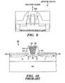
- FIG. 9is a side-sectional schematic view of a pFET semiconductor device structure according to the present invention.
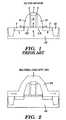
- FIG. 10is a side-sectional schematic view of an nFET device according to the prior art. STI regions are not shown. Also not shown in FIG. 10 are various known stress liners as discussed, for example, in the '866, '808 and '584 U.S. Patents previously mentioned.
- FIGS. 1-8A preferred embodiment and best mode of the present invention will now be described with reference to FIGS. 1-8 , for making a semiconductor device structure including an nFET.
- Applicant's methodis applicable for producing a semiconductor device structure including a pFET. See FIG. 9 , for example.
- a substrate 10which has formed thereon an oxide layer 3 disposed below a gate G 1 provided with sidewall spacers SP, oxide layers 5 disposed between the gate G 1 and the spacers SP and between the spacers SP and the substrate 10 , suitably implanted source and drain regions S, D formed adjacent to the gate, an isolation region STI disposed in the substrate 10 , and silicides 7 disposed on the gate, and source and drain regions S,D. Also shown are lightly doped source and drain regions LDD.
- the device of FIG. 1is conventional and can correspond, for example, to the prior art SOI-nFET device shown in FIG. 8 (STI regions are not shown in FIG. 8 ).
- the semiconductor substrate 10is, for example, a bulk silicon (Si) substrate or a silicon-on-insulator (SOI) substrate.
- the substrate 10is a hybrid substrate which includes more than one surface orientation.
- the substratealternatively includes a semiconductor material other than Si, such as Ge or any combination of Group III-V elements or Group II-V elements.
- an isolation schemeis carried out. As is well known in semiconductor manufacturing, the isolation scheme is used to separate selected semiconductor devices electrically from each other.
- the isolation schemeis a standard or a modified shallow trench isolation (STI) scheme.
- An isolation region STIis shown in FIG. 1 .
- the isolationis accomplished using a LOCOS process or mesa isolation scheme, as is well known in the art of fabricating semiconductor devices.
- LOCOS processor mesa isolation scheme
- a conventional gate oxide pre-cleaning processis performed.
- various conventional gate oxide processesmay be used to fabricate devices having different gate oxide thicknesses.
- the gate oxide 3is formed, for example, using a conventional thermal oxidation process.
- the gate oxide 3is formed using N 2 O, NO, O 2 or any combination of them.
- the oxide 3may be nitridized using a conventional plasma process.
- the gate oxide 3is formed using a base oxide followed by deposition of a high k gate dielectric material such as aluminum oxide, or hafnium oxide, or another high k gate dielectric.
- the gate dielectric materialhas, for example, one approximately (+10%) uniform thickness selected from a range of about (+10%) 0.6 nm to about 7 nm.
- the gate electrode or gate G 1is formed conventionally.
- the gate G 1is formed from a polysilicon layer (not shown) deposited by a low pressure chemical vapor deposition (LPCVD) using a reactant gas such as silane (SiH 4 ).
- LPCVDlow pressure chemical vapor deposition
- the thickness (height) of the layeris between about 1000 and 3000 Angstroms.
- the layeris then conductively doped n-type by ion implanting arsenic (As 75 ) or phosphorus (P 31 ).
- the final dopant concentration of the layer after implantationsis preferred between about 1.0 E 18 and 1.0 E 21 atoms/cm 3 .
- the polysilicon layerwhich includes forming the gate electrode G 1 over the device areas.
- the device areasinclude a channel C.
- the polysilicon layeris plasma etched using a reactive ion etching (RIE) or a high density plasma (HDP) etching and an etchant gas such as chlorine (Cl 2 ).
- RIEreactive ion etching
- HDPhigh density plasma
- lightly doped source and drain (LDD) or extension areasare formed in the device areas adjacent to the gate electrode by ion implantation, using a second conductive type dopant, such as As or P.
- a second conductive type dopantsuch as As or P.
- Polysilicon sidewall reoxidation layers 5 or offset spacerscould be used to offset the LDD implants.
- the LDD areasare doped to a concentration of between about 1.0 E 19 and 5.0 E 20 atoms/cm 3 .
- a conformal insulating layer(not shown) is deposited using conventional deposition techniques (e.g., CVD) and anisotropically plasma etched back to form sidewall spacers SP on the sidewalls of the gate electrode G 1 and/or on oxide layers 5 .
- FIG. 1shows the spacers SP disposed on the oxide layers 5 formed on the gate G 1 and on substrate 10 .
- the insulating layer for forming the spacers SPis silicon oxide (SiO 2 ) and is deposited by a low pressure CVD (LPCVD) using tetraethosiloxane (TEOS) as the reactant gas, and is deposited to a preferred thickness of about ( ⁇ 10%) 200 Angstroms to about ( ⁇ 10%) 1000 Angstroms.
- LPCVDlow pressure CVD
- TEOStetraethosiloxane
- Other optionsinclude nitride spacers or a combination of multiple spacers with nitride and oxide materials.
- a conventional etch backis then carried out using a reactive ion etching (RIE) and an etchant gas such as carbon tetrafluoride (CF 4 ) and hydrogen H 2 or methylfluoride (CHF 3 ), which etches the SiO 2 layer selectively to the silicon substrate and polysilicon gate electrode.
- RIEreactive ion etching
- etchant gassuch as carbon tetrafluoride (CF 4 ) and hydrogen H 2 or methylfluoride (CHF 3 , which etches the SiO 2 layer selectively to the silicon substrate and polysilicon gate electrode.
- Heavily doped source and drain contact areas S,Dare then formed in the device areas adjacent to the insulating sidewall spacers SP by ion implanting a second conductive type dopant, such as arsenic.
- the contact areasare doped to a final concentration of between about 1.0 E 18 and 1.0 E 21 atoms/cm 3 . Any residual native oxide remaining on the source and drain
- the nFETis then silicided in any conventional fashion, so that silicides 7 are formed at locations as shown in FIG. 1 , to form the nFET device of FIG. 1 . More details for various parts of the structure of FIG. 1 are shown, for example, in the prior art nFET device structure shown in FIG. 10 and described in U.S. Pat. No. 6,930,030 B2 previously incorporated herein by reference.
- FIG. 1The foregoing description for FIG. 1 is with respect to nFET devices.
- polarity type of dopantsis reversed when pFET devices are used, and that conventional masking, patterning etc. are required during processing.
- a first conformal dielectric stress layer or film 20is deposited over the device formed on the substrate 10 . More specifically, deposit the layer 20 over the silicided gate with spacers SP, silicided source and drain regions, and the isolation regions STI.
- the layer 20is preferably silicon nitride (Si 3 N 4 ) and is deposited to one approximately ( ⁇ 10%) uniform thickness selected from a range of thicknesses from about 20 nanometers to about 70 nanometers.
- the Si 3 N 4can be deposited by conventional chemical vapor deposition (CVD), HDP, ALD or other conventional deposition techniques.
- the Si 3 N 4has a high tensile stress such as a stress in a range from about 1 GPa to about 3 GPa.
- the stress layer 20 disposed over the silicided gate G 1 with spacers SP, the silicided source and drain regions S,D and the STI regionsis accomplished, for example, by means of depositing an insulating layer ILD.
- the layer ILDis any suitable oxide such as silicon oxide and deposited by any suitable conventional techniques such as CVD.
- the insulating layer ILDhas a thickness (above a top surface 21 of the layer 20 ), which thickness is approximately twice the thickness of the layer 20 .
- Removalis accomplished, for example, by means of a conventional reactive ion etching (RIE) or CMP or other conventional technique.
- RIEreactive ion etching
- the trench 40surrounds portions of the gate stack provided with oxide layers 5 as shown in FIG. 5 .
- the trench 40extends approximately half-way along the height of the gate stack G 1 , 7 , 3 .
- the trench 40can have, for example, a rectangular area in a space between each spacer SP 1 and the oxide layer 5 .
- a compressive stress materialin the trench, by means of any conventional technique such as CVD, to result in the structure of FIG. 6 .
- CVDchemical vapor deposition
- Removalis accomplished by any suitable etching such as RIE or CMP.
- FIG. 8shows a simulation of the relationship between stress (Y-axis) and location (X-axis) in the channel C, for an nFET semiconductor device structure according to the present invention.
- a center of the channel Cis located at a distance of approximately 0.35 microns across width of the channel C.
- Applicant's inventionincludes a method for making a semiconductor device structure including an nFET device and a pFET device. See FIG. 9 .
- a tensile stress material 300fills a trench into which a gate stack provided with sidewall (e.g., oxide) layers extends.
- the gate stackincludes a gate electrode, an oxide layer disposed below the gate, and a silicide disposed above the gate, all as shown in FIG. 9 .
Landscapes
- Insulated Gate Type Field-Effect Transistor (AREA)
- Metal-Oxide And Bipolar Metal-Oxide Semiconductor Integrated Circuits (AREA)
- Thin Film Transistor (AREA)
Abstract
Description
Claims (7)
Priority Applications (1)
| Application Number | Priority Date | Filing Date | Title |
|---|---|---|---|
| US12/643,482US7935993B2 (en) | 2006-01-10 | 2009-12-21 | Semiconductor device structure having enhanced performance FET device |
Applications Claiming Priority (2)
| Application Number | Priority Date | Filing Date | Title |
|---|---|---|---|
| US11/306,745US7635620B2 (en) | 2006-01-10 | 2006-01-10 | Semiconductor device structure having enhanced performance FET device |
| US12/643,482US7935993B2 (en) | 2006-01-10 | 2009-12-21 | Semiconductor device structure having enhanced performance FET device |
Related Parent Applications (1)
| Application Number | Title | Priority Date | Filing Date |
|---|---|---|---|
| US11/306,745DivisionUS7635620B2 (en) | 2006-01-10 | 2006-01-10 | Semiconductor device structure having enhanced performance FET device |
Publications (2)
| Publication Number | Publication Date |
|---|---|
| US20100096673A1 US20100096673A1 (en) | 2010-04-22 |
| US7935993B2true US7935993B2 (en) | 2011-05-03 |
Family
ID=39740764
Family Applications (2)
| Application Number | Title | Priority Date | Filing Date |
|---|---|---|---|
| US11/306,745Expired - Fee RelatedUS7635620B2 (en) | 2006-01-10 | 2006-01-10 | Semiconductor device structure having enhanced performance FET device |
| US12/643,482Expired - Fee RelatedUS7935993B2 (en) | 2006-01-10 | 2009-12-21 | Semiconductor device structure having enhanced performance FET device |
Family Applications Before (1)
| Application Number | Title | Priority Date | Filing Date |
|---|---|---|---|
| US11/306,745Expired - Fee RelatedUS7635620B2 (en) | 2006-01-10 | 2006-01-10 | Semiconductor device structure having enhanced performance FET device |
Country Status (1)
| Country | Link |
|---|---|
| US (2) | US7635620B2 (en) |
Cited By (2)
| Publication number | Priority date | Publication date | Assignee | Title |
|---|---|---|---|---|
| US8995177B1 (en)* | 2009-12-02 | 2015-03-31 | Altera Corporation | Integrated circuits with asymmetric transistors |
| US10043903B2 (en) | 2015-12-21 | 2018-08-07 | Samsung Electronics Co., Ltd. | Semiconductor devices with source/drain stress liner |
Families Citing this family (20)
| Publication number | Priority date | Publication date | Assignee | Title |
|---|---|---|---|---|
| US7445978B2 (en)* | 2005-05-04 | 2008-11-04 | Chartered Semiconductor Manufacturing, Ltd | Method to remove spacer after salicidation to enhance contact etch stop liner stress on MOS |
| US9048180B2 (en)* | 2006-05-16 | 2015-06-02 | Texas Instruments Incorporated | Low stress sacrificial cap layer |
| US7935587B2 (en) | 2006-06-09 | 2011-05-03 | Taiwan Semiconductor Manufacturing Company, Ltd. | Advanced forming method and structure of local mechanical strained transistor |
| JP5092340B2 (en)* | 2006-10-12 | 2012-12-05 | 富士通セミコンダクター株式会社 | Semiconductor device and manufacturing method thereof |
| US7601574B2 (en)* | 2006-10-25 | 2009-10-13 | Globalfoundries Inc. | Methods for fabricating a stress enhanced MOS transistor |
| US7879663B2 (en)* | 2007-03-08 | 2011-02-01 | Freescale Semiconductor, Inc. | Trench formation in a semiconductor material |
| US7611935B2 (en)* | 2007-05-24 | 2009-11-03 | Advanced Micro Devices, Inc. | Gate straining in a semiconductor device |
| JP5309619B2 (en) | 2008-03-07 | 2013-10-09 | ソニー株式会社 | Semiconductor device and manufacturing method thereof |
| US8153532B1 (en)* | 2008-12-04 | 2012-04-10 | Hrl Laboratories, Llc | Bilayer dielectric interconnection process |
| US8030154B1 (en)* | 2010-08-03 | 2011-10-04 | International Business Machines Corporation | Method for forming a protection layer over metal semiconductor contact and structure formed thereon |
| KR101815527B1 (en)* | 2010-10-07 | 2018-01-05 | 삼성전자주식회사 | Semiconductor device and method for manufacturing the same |
| US8530319B2 (en) | 2010-10-14 | 2013-09-10 | International Business Machines Corporation | Vertical silicide e-fuse |
| US8470674B2 (en) | 2011-01-03 | 2013-06-25 | International Business Machines Corporation | Structure, method and system for complementary strain fill for integrated circuit chips |
| US9041076B2 (en)* | 2013-02-03 | 2015-05-26 | International Business Machines Corporation | Partial sacrificial dummy gate with CMOS device with high-k metal gate |
| CN103855024A (en)* | 2012-12-05 | 2014-06-11 | 中芯国际集成电路制造(上海)有限公司 | NMOS transistor, CMOS transistor and manufacturing method of NMOS transistor and CMOS transistor |
| US9728637B2 (en) | 2013-11-14 | 2017-08-08 | Taiwan Semiconductor Manufacturing Co., Ltd. | Mechanism for forming semiconductor device with gate |
| US10418453B2 (en) | 2017-11-22 | 2019-09-17 | Taiwan Semiconductor Manufacturing Co., Ltd. | Forming metal contacts on metal gates |
| DE112017008080T5 (en) | 2017-12-26 | 2020-07-09 | Intel Corporation | STACKED TRANSISTORS WITH LAST TRAINED CONTACT |
| US11393722B2 (en) | 2018-01-12 | 2022-07-19 | Intel Corporation | Isolation wall stressor structures to improve channel stress and their methods of fabrication |
| US11430814B2 (en) | 2018-03-05 | 2022-08-30 | Intel Corporation | Metallization structures for stacked device connectivity and their methods of fabrication |
Citations (115)
| Publication number | Priority date | Publication date | Assignee | Title |
|---|---|---|---|---|
| US3602841A (en) | 1970-06-18 | 1971-08-31 | Ibm | High frequency bulk semiconductor amplifiers and oscillators |
| US4665415A (en) | 1985-04-24 | 1987-05-12 | International Business Machines Corporation | Semiconductor device with hole conduction via strained lattice |
| US4853076A (en) | 1983-12-29 | 1989-08-01 | Massachusetts Institute Of Technology | Semiconductor thin films |
| US4855245A (en) | 1985-09-13 | 1989-08-08 | Siemens Aktiengesellschaft | Method of manufacturing integrated circuit containing bipolar and complementary MOS transistors on a common substrate |
| US4952524A (en) | 1989-05-05 | 1990-08-28 | At&T Bell Laboratories | Semiconductor device manufacture including trench formation |
| US4958213A (en) | 1987-12-07 | 1990-09-18 | Texas Instruments Incorporated | Method for forming a transistor base region under thick oxide |
| US4969023A (en) | 1987-08-24 | 1990-11-06 | Asea Brown Boveri Ab | SOS transistor structure |
| US5006913A (en) | 1988-11-05 | 1991-04-09 | Mitsubishi Denki Kabushiki Kaisha | Stacked type semiconductor device |
| US5060030A (en) | 1990-07-18 | 1991-10-22 | Raytheon Company | Pseudomorphic HEMT having strained compensation layer |
| US5081513A (en) | 1991-02-28 | 1992-01-14 | Xerox Corporation | Electronic device with recovery layer proximate to active layer |
| US5108843A (en) | 1988-11-30 | 1992-04-28 | Ricoh Company, Ltd. | Thin film semiconductor and process for producing the same |
| US5134085A (en) | 1991-11-21 | 1992-07-28 | Micron Technology, Inc. | Reduced-mask, split-polysilicon CMOS process, incorporating stacked-capacitor cells, for fabricating multi-megabit dynamic random access memories |
| US5268330A (en) | 1992-12-11 | 1993-12-07 | International Business Machines Corporation | Process for improving sheet resistance of an integrated circuit device gate |
| US5310446A (en) | 1990-01-10 | 1994-05-10 | Ricoh Company, Ltd. | Method for producing semiconductor film |
| US5354695A (en) | 1992-04-08 | 1994-10-11 | Leedy Glenn J | Membrane dielectric isolation IC fabrication |
| US5371399A (en) | 1991-06-14 | 1994-12-06 | International Business Machines Corporation | Compound semiconductor having metallic inclusions and devices fabricated therefrom |
| US5391510A (en) | 1992-02-28 | 1995-02-21 | International Business Machines Corporation | Formation of self-aligned metal gate FETs using a benignant removable gate material during high temperature steps |
| US5459346A (en) | 1988-06-28 | 1995-10-17 | Ricoh Co., Ltd. | Semiconductor substrate with electrical contact in groove |
| US5557122A (en) | 1995-05-12 | 1996-09-17 | Alliance Semiconductors Corporation | Semiconductor electrode having improved grain structure and oxide growth properties |
| US5561302A (en) | 1994-09-26 | 1996-10-01 | Motorola, Inc. | Enhanced mobility MOSFET device and method |
| US5583369A (en) | 1992-07-06 | 1996-12-10 | Semiconductor Energy Laboratory Co., Ltd. | Semiconductor device and method for forming the same |
| US5592009A (en) | 1994-09-01 | 1997-01-07 | Mitsubishi Denki Kabushiki Kaisha | Semiconductor device having a floating node that can maintain a predetermined potential for long time, a semiconductor memory device having high data maintenance performance, and a method of manufacturing thereof |
| US5670798A (en) | 1995-03-29 | 1997-09-23 | North Carolina State University | Integrated heterostructures of Group III-V nitride semiconductor materials including epitaxial ohmic contact non-nitride buffer layer and methods of fabricating same |
| US5679965A (en) | 1995-03-29 | 1997-10-21 | North Carolina State University | Integrated heterostructures of Group III-V nitride semiconductor materials including epitaxial ohmic contact, non-nitride buffer layer and methods of fabricating same |
| US5698869A (en) | 1994-09-13 | 1997-12-16 | Kabushiki Kaisha Toshiba | Insulated-gate transistor having narrow-bandgap-source |
| US5841170A (en) | 1996-04-25 | 1998-11-24 | Sharp Kabushiki Kaisha | Field effect transistor and CMOS element having dopant exponentially graded in channel |
| US5861651A (en) | 1997-02-28 | 1999-01-19 | Lucent Technologies Inc. | Field effect devices and capacitors with improved thin film dielectrics and method for making same |
| US5880040A (en) | 1996-04-15 | 1999-03-09 | Macronix International Co., Ltd. | Gate dielectric based on oxynitride grown in N2 O and annealed in NO |
| US5940736A (en) | 1997-03-11 | 1999-08-17 | Lucent Technologies Inc. | Method for forming a high quality ultrathin gate oxide layer |
| US5940716A (en) | 1996-03-15 | 1999-08-17 | Samsung Electronics Co., Ltd. | Methods of forming trench isolation regions using repatterned trench masks |
| US5960297A (en) | 1997-07-02 | 1999-09-28 | Kabushiki Kaisha Toshiba | Shallow trench isolation structure and method of forming the same |
| US5989978A (en) | 1998-07-16 | 1999-11-23 | Chartered Semiconductor Manufacturing, Ltd. | Shallow trench isolation of MOSFETS with reduced corner parasitic currents |
| US6008126A (en) | 1992-04-08 | 1999-12-28 | Elm Technology Corporation | Membrane dielectric isolation IC fabrication |
| US6025280A (en) | 1997-04-28 | 2000-02-15 | Lucent Technologies Inc. | Use of SiD4 for deposition of ultra thin and controllable oxides |
| US6066545A (en) | 1997-12-09 | 2000-05-23 | Texas Instruments Incorporated | Birdsbeak encroachment using combination of wet and dry etch for isolation nitride |
| US6090684A (en) | 1998-07-31 | 2000-07-18 | Hitachi, Ltd. | Method for manufacturing semiconductor device |
| US6107143A (en) | 1998-03-02 | 2000-08-22 | Samsung Electronics Co., Ltd. | Method for forming a trench isolation structure in an integrated circuit |
| US6117722A (en) | 1999-02-18 | 2000-09-12 | Taiwan Semiconductor Manufacturing Company | SRAM layout for relaxing mechanical stress in shallow trench isolation technology and method of manufacture thereof |
| US6133071A (en) | 1997-10-15 | 2000-10-17 | Nec Corporation | Semiconductor device with plate heat sink free from cracks due to thermal stress and process for assembling it with package |
| US6165383A (en) | 1998-04-10 | 2000-12-26 | Organic Display Technology | Useful precursors for organic electroluminescent materials and devices made from such materials |
| US6221735B1 (en) | 2000-02-15 | 2001-04-24 | Philips Semiconductors, Inc. | Method for eliminating stress induced dislocations in CMOS devices |
| US6228694B1 (en) | 1999-06-28 | 2001-05-08 | Intel Corporation | Method of increasing the mobility of MOS transistors by use of localized stress regions |
| US6255169B1 (en) | 1999-02-22 | 2001-07-03 | Advanced Micro Devices, Inc. | Process for fabricating a high-endurance non-volatile memory device |
| US6255695B1 (en) | 1996-09-20 | 2001-07-03 | Semiconductor Energy Laboratory Co., Ltd. | TFT CMOS logic circuit having source/drain electrodes of differing spacing from the gate electrode for decreasing wiring capacitance and power consumption |
| US6261964B1 (en) | 1997-03-14 | 2001-07-17 | Micron Technology, Inc. | Material removal method for forming a structure |
| US6265317B1 (en) | 2001-01-09 | 2001-07-24 | Taiwan Semiconductor Manufacturing Company | Top corner rounding for shallow trench isolation |
| US20010009784A1 (en) | 1998-01-09 | 2001-07-26 | Yanjun Ma | Structure and method of making a sub-micron MOS transistor |
| US6274444B1 (en) | 1999-07-30 | 2001-08-14 | United Microelectronics Corp. | Method for forming mosfet |
| US6281532B1 (en) | 1999-06-28 | 2001-08-28 | Intel Corporation | Technique to obtain increased channel mobilities in NMOS transistors by gate electrode engineering |
| US6284623B1 (en) | 1999-10-25 | 2001-09-04 | Peng-Fei Zhang | Method of fabricating semiconductor devices using shallow trench isolation with reduced narrow channel effect |
| US6284626B1 (en) | 1999-04-06 | 2001-09-04 | Vantis Corporation | Angled nitrogen ion implantation for minimizing mechanical stress on side walls of an isolation trench |
| US6319794B1 (en) | 1998-10-14 | 2001-11-20 | International Business Machines Corporation | Structure and method for producing low leakage isolation devices |
| US6362082B1 (en) | 1999-06-28 | 2002-03-26 | Intel Corporation | Methodology for control of short channel effects in MOS transistors |
| US6361885B1 (en) | 1998-04-10 | 2002-03-26 | Organic Display Technology | Organic electroluminescent materials and device made from such materials |
| US6368931B1 (en) | 2000-03-27 | 2002-04-09 | Intel Corporation | Thin tensile layers in shallow trench isolation and method of making same |
| US20020063292A1 (en) | 2000-11-29 | 2002-05-30 | Mark Armstrong | CMOS fabrication process utilizing special transistor orientation |
| US6403486B1 (en) | 2001-04-30 | 2002-06-11 | Taiwan Semiconductor Manufacturing Company | Method for forming a shallow trench isolation |
| US6403975B1 (en) | 1996-04-09 | 2002-06-11 | Max-Planck Gesellschaft Zur Forderung Der Wissenschafteneev | Semiconductor components, in particular photodetectors, light emitting diodes, optical modulators and waveguides with multilayer structures grown on silicon substrates |
| US6406973B1 (en) | 1999-06-29 | 2002-06-18 | Hyundai Electronics Industries Co., Ltd. | Transistor in a semiconductor device and method of manufacturing the same |
| US20020086472A1 (en) | 2000-12-29 | 2002-07-04 | Brian Roberds | Technique to obtain high mobility channels in MOS transistors by forming a strain layer on an underside of a channel |
| US20020086497A1 (en) | 2000-12-30 | 2002-07-04 | Kwok Siang Ping | Beaker shape trench with nitride pull-back for STI |
| US20020090791A1 (en) | 1999-06-28 | 2002-07-11 | Brian S. Doyle | Method for reduced capacitance interconnect system using gaseous implants into the ild |
| US6461936B1 (en) | 2002-01-04 | 2002-10-08 | Infineon Technologies Ag | Double pullback method of filling an isolation trench |
| US6468872B1 (en) | 1999-08-12 | 2002-10-22 | L.G. Philips Lcd Co., Ltd | Method of fabricating a thin film transistor |
| US6476462B2 (en) | 1999-12-28 | 2002-11-05 | Texas Instruments Incorporated | MOS-type semiconductor device and method for making same |
| US6483171B1 (en) | 1999-08-13 | 2002-11-19 | Micron Technology, Inc. | Vertical sub-micron CMOS transistors on (110), (111), (311), (511), and higher order surfaces of bulk, SOI and thin film structures and method of forming same |
| US6493497B1 (en) | 2000-09-26 | 2002-12-10 | Motorola, Inc. | Electro-optic structure and process for fabricating same |
| US6498358B1 (en) | 2001-07-20 | 2002-12-24 | Motorola, Inc. | Structure and method for fabricating an electro-optic system having an electrochromic diffraction grating |
| US6501121B1 (en) | 2000-11-15 | 2002-12-31 | Motorola, Inc. | Semiconductor structure |
| US6506652B2 (en) | 1998-11-13 | 2003-01-14 | Intel Corporation | Method of recessing spacers to improved salicide resistance on polysilicon gates |
| US20030032261A1 (en) | 2001-08-08 | 2003-02-13 | Ling-Yen Yeh | Method of preventing threshold voltage of MOS transistor from being decreased by shallow trench isolation formation |
| US20030040158A1 (en) | 2001-08-21 | 2003-02-27 | Nec Corporation | Semiconductor device and method of fabricating the same |
| US6531740B2 (en) | 2001-07-17 | 2003-03-11 | Motorola, Inc. | Integrated impedance matching and stability network |
| US6531369B1 (en) | 2000-03-01 | 2003-03-11 | Applied Micro Circuits Corporation | Heterojunction bipolar transistor (HBT) fabrication using a selectively deposited silicon germanium (SiGe) |
| US20030057184A1 (en) | 2001-09-22 | 2003-03-27 | Shiuh-Sheng Yu | Method for pull back SiN to increase rounding effect in a shallow trench isolation process |
| US20030067035A1 (en) | 2001-09-28 | 2003-04-10 | Helmut Tews | Gate processing method with reduced gate oxide corner and edge thinning |
| US20030129791A1 (en) | 1999-04-30 | 2003-07-10 | Semiconductor Energy Laboratory Co., Ltd. | Semiconductor device and manufacturing method thereof |
| US6605498B1 (en) | 2002-03-29 | 2003-08-12 | Intel Corporation | Semiconductor transistor having a backfilled channel material |
| US6621131B2 (en) | 2001-11-01 | 2003-09-16 | Intel Corporation | Semiconductor transistor having a stressed channel |
| US6621392B1 (en) | 2002-04-25 | 2003-09-16 | International Business Machines Corporation | Micro electromechanical switch having self-aligned spacers |
| US20030181005A1 (en) | 2002-03-19 | 2003-09-25 | Kiyota Hachimine | Semiconductor device and a method of manufacturing the same |
| US6635506B2 (en) | 2001-11-07 | 2003-10-21 | International Business Machines Corporation | Method of fabricating micro-electromechanical switches on CMOS compatible substrates |
| US20040029323A1 (en) | 2000-11-22 | 2004-02-12 | Akihiro Shimizu | Semiconductor device and method for fabricating the same |
| US20040051144A1 (en) | 2002-09-17 | 2004-03-18 | Clair Webb | N-p butting connections on SOI substrates |
| US6717216B1 (en) | 2002-12-12 | 2004-04-06 | International Business Machines Corporation | SOI based field effect transistor having a compressive film in undercut area under the channel and a method of making the device |
| US20040113217A1 (en) | 2002-12-12 | 2004-06-17 | International Business Machines Corporation | Stress inducing spacers |
| US20040113174A1 (en) | 2002-12-12 | 2004-06-17 | International Business Machines Corporation | Isolation structures for imposing stress patterns |
| US20040173815A1 (en) | 2003-03-04 | 2004-09-09 | Yee-Chia Yeo | Strained-channel transistor structure with lattice-mismatched zone |
| US6806584B2 (en) | 2002-10-21 | 2004-10-19 | International Business Machines Corporation | Semiconductor device structure including multiple fets having different spacer widths |
| US6815278B1 (en) | 2003-08-25 | 2004-11-09 | International Business Machines Corporation | Ultra-thin silicon-on-insulator and strained-silicon-direct-on-insulator with hybrid crystal orientations |
| US20040238914A1 (en) | 2003-05-30 | 2004-12-02 | International Business Machines Corporation | STI stress modification by nitrogen plasma treatment for improving performance in small width devices |
| US6831292B2 (en) | 2001-09-21 | 2004-12-14 | Amberwave Systems Corporation | Semiconductor structures employing strained material layers with defined impurity gradients and methods for fabricating same |
| US20040262784A1 (en) | 2003-06-30 | 2004-12-30 | International Business Machines Corporation | High performance cmos device structures and method of manufacture |
| US20050017304A1 (en) | 2003-06-13 | 2005-01-27 | Daisuke Matsushita | Field effect transistor and method of manufacturing the same |
| US6869866B1 (en) | 2003-09-22 | 2005-03-22 | International Business Machines Corporation | Silicide proximity structures for CMOS device performance improvements |
| US20050082634A1 (en) | 2003-10-16 | 2005-04-21 | International Business Machines Corporation | High performance strained cmos devices |
| US20050093030A1 (en) | 2003-10-30 | 2005-05-05 | Doris Bruce B. | Structure and method to enhance both nFET and pFET performance using different kinds of stressed layers |
| US6890808B2 (en) | 2003-09-10 | 2005-05-10 | International Business Machines Corporation | Method and structure for improved MOSFETs using poly/silicide gate height control |
| US20050098829A1 (en) | 2003-11-06 | 2005-05-12 | Doris Bruce B. | High mobility CMOS circuits |
| US20050098234A1 (en) | 2003-11-04 | 2005-05-12 | Shu Nakaharai | Element fabrication substrate |
| US20050106799A1 (en) | 2003-11-14 | 2005-05-19 | International Business Machines Corporation | Stressed semiconductor device structures having granular semiconductor material |
| US20050139929A1 (en) | 2003-12-30 | 2005-06-30 | Rost Timothy A. | Transistor design and layout for performance improvement with strain |
| US20050145954A1 (en) | 2004-01-05 | 2005-07-07 | International Business Machines Corporation | Structures and methods for making strained mosfets |
| US6930030B2 (en) | 2003-06-03 | 2005-08-16 | International Business Machines Corporation | Method of forming an electronic device on a recess in the surface of a thin film of silicon etched to a precise thickness |
| US20050194699A1 (en) | 2004-03-03 | 2005-09-08 | International Business Machines Corporation | Mobility enhanced cmos devices |
| US20050236668A1 (en) | 2004-04-23 | 2005-10-27 | International Business Machines Corporation | STRUCTURES AND METHODS FOR MANUFACTURING OF DISLOCATION FREE STRESSED CHANNELS IN BULK SILICON AND SOI CMOS DEVICES BY GATE STRESS ENGINEERING WITH SiGe AND/OR Si:C |
| US20050245017A1 (en) | 2003-10-30 | 2005-11-03 | Belyansky Michael P | Structure and method to improve channel mobility by gate electrode stress modification |
| US6964892B2 (en) | 2000-01-21 | 2005-11-15 | International Business Machines Corporation | N-channel metal oxide semiconductor (NMOS) driver circuit and method of making same |
| US20050260806A1 (en)* | 2004-05-19 | 2005-11-24 | Taiwan Semiconductor Manufacturing Co., Ltd. | High performance strained channel mosfets by coupled stress effects |
| US20060022266A1 (en) | 2004-07-30 | 2006-02-02 | International Business Machines Corporation | Manufacturable recessed strained rsd structure and process for advanced cmos |
| US6998657B2 (en) | 2003-10-21 | 2006-02-14 | Micron Technology, Inc. | Single poly CMOS imager |
| US20060057787A1 (en) | 2002-11-25 | 2006-03-16 | Doris Bruce B | Strained finfet cmos device structures |
| US20060060925A1 (en) | 2004-09-17 | 2006-03-23 | International Business Machines Corporation | Semiconductor device structure with active regions having different surface directions and methods |
| US20060094212A1 (en) | 2004-10-13 | 2006-05-04 | Samsung Electronics Co., Ltd. | Thin film transistor and method of manufacturing the same |
| US20060246641A1 (en) | 2005-04-29 | 2006-11-02 | Thorsten Kammler | Technique for forming a contact insulation layer with enhanced stress transfer efficiency |
Family Cites Families (1)
| Publication number | Priority date | Publication date | Assignee | Title |
|---|---|---|---|---|
| JPS6476755A (en) | 1987-09-18 | 1989-03-22 | Hitachi Ltd | Semiconductor device |
- 2006
- 2006-01-10USUS11/306,745patent/US7635620B2/ennot_activeExpired - Fee Related
- 2009
- 2009-12-21USUS12/643,482patent/US7935993B2/ennot_activeExpired - Fee Related
Patent Citations (138)
| Publication number | Priority date | Publication date | Assignee | Title |
|---|---|---|---|---|
| US3602841A (en) | 1970-06-18 | 1971-08-31 | Ibm | High frequency bulk semiconductor amplifiers and oscillators |
| US4853076A (en) | 1983-12-29 | 1989-08-01 | Massachusetts Institute Of Technology | Semiconductor thin films |
| US4665415A (en) | 1985-04-24 | 1987-05-12 | International Business Machines Corporation | Semiconductor device with hole conduction via strained lattice |
| US4855245A (en) | 1985-09-13 | 1989-08-08 | Siemens Aktiengesellschaft | Method of manufacturing integrated circuit containing bipolar and complementary MOS transistors on a common substrate |
| US4969023A (en) | 1987-08-24 | 1990-11-06 | Asea Brown Boveri Ab | SOS transistor structure |
| US4958213A (en) | 1987-12-07 | 1990-09-18 | Texas Instruments Incorporated | Method for forming a transistor base region under thick oxide |
| US5459346A (en) | 1988-06-28 | 1995-10-17 | Ricoh Co., Ltd. | Semiconductor substrate with electrical contact in groove |
| US5565697A (en) | 1988-06-28 | 1996-10-15 | Ricoh Company, Ltd. | Semiconductor structure having island forming grooves |
| US5006913A (en) | 1988-11-05 | 1991-04-09 | Mitsubishi Denki Kabushiki Kaisha | Stacked type semiconductor device |
| US5108843A (en) | 1988-11-30 | 1992-04-28 | Ricoh Company, Ltd. | Thin film semiconductor and process for producing the same |
| US4952524A (en) | 1989-05-05 | 1990-08-28 | At&T Bell Laboratories | Semiconductor device manufacture including trench formation |
| US5310446A (en) | 1990-01-10 | 1994-05-10 | Ricoh Company, Ltd. | Method for producing semiconductor film |
| US5060030A (en) | 1990-07-18 | 1991-10-22 | Raytheon Company | Pseudomorphic HEMT having strained compensation layer |
| US5081513A (en) | 1991-02-28 | 1992-01-14 | Xerox Corporation | Electronic device with recovery layer proximate to active layer |
| US5471948A (en) | 1991-06-14 | 1995-12-05 | International Business Machines Corporation | Method of making a compound semiconductor having metallic inclusions |
| US5371399A (en) | 1991-06-14 | 1994-12-06 | International Business Machines Corporation | Compound semiconductor having metallic inclusions and devices fabricated therefrom |
| US5134085A (en) | 1991-11-21 | 1992-07-28 | Micron Technology, Inc. | Reduced-mask, split-polysilicon CMOS process, incorporating stacked-capacitor cells, for fabricating multi-megabit dynamic random access memories |
| US5391510A (en) | 1992-02-28 | 1995-02-21 | International Business Machines Corporation | Formation of self-aligned metal gate FETs using a benignant removable gate material during high temperature steps |
| US5354695A (en) | 1992-04-08 | 1994-10-11 | Leedy Glenn J | Membrane dielectric isolation IC fabrication |
| US5840593A (en) | 1992-04-08 | 1998-11-24 | Elm Technology Corporation | Membrane dielectric isolation IC fabrication |
| US6008126A (en) | 1992-04-08 | 1999-12-28 | Elm Technology Corporation | Membrane dielectric isolation IC fabrication |
| US5571741A (en) | 1992-04-08 | 1996-11-05 | Leedy; Glenn J. | Membrane dielectric isolation IC fabrication |
| US5946559A (en) | 1992-04-08 | 1999-08-31 | Elm Technology Corporation | Membrane dielectric isolation IC fabrication |
| US5592007A (en) | 1992-04-08 | 1997-01-07 | Leedy; Glenn J. | Membrane dielectric isolation transistor fabrication |
| US5592018A (en) | 1992-04-08 | 1997-01-07 | Leedy; Glenn J. | Membrane dielectric isolation IC fabrication |
| US5583369A (en) | 1992-07-06 | 1996-12-10 | Semiconductor Energy Laboratory Co., Ltd. | Semiconductor device and method for forming the same |
| US5268330A (en) | 1992-12-11 | 1993-12-07 | International Business Machines Corporation | Process for improving sheet resistance of an integrated circuit device gate |
| US5592009A (en) | 1994-09-01 | 1997-01-07 | Mitsubishi Denki Kabushiki Kaisha | Semiconductor device having a floating node that can maintain a predetermined potential for long time, a semiconductor memory device having high data maintenance performance, and a method of manufacturing thereof |
| US5698869A (en) | 1994-09-13 | 1997-12-16 | Kabushiki Kaisha Toshiba | Insulated-gate transistor having narrow-bandgap-source |
| US5683934A (en) | 1994-09-26 | 1997-11-04 | Motorola, Inc. | Enhanced mobility MOSFET device and method |
| US5561302A (en) | 1994-09-26 | 1996-10-01 | Motorola, Inc. | Enhanced mobility MOSFET device and method |
| US5670798A (en) | 1995-03-29 | 1997-09-23 | North Carolina State University | Integrated heterostructures of Group III-V nitride semiconductor materials including epitaxial ohmic contact non-nitride buffer layer and methods of fabricating same |
| US6046464A (en) | 1995-03-29 | 2000-04-04 | North Carolina State University | Integrated heterostructures of group III-V nitride semiconductor materials including epitaxial ohmic contact comprising multiple quantum well |
| US5679965A (en) | 1995-03-29 | 1997-10-21 | North Carolina State University | Integrated heterostructures of Group III-V nitride semiconductor materials including epitaxial ohmic contact, non-nitride buffer layer and methods of fabricating same |
| US5557122A (en) | 1995-05-12 | 1996-09-17 | Alliance Semiconductors Corporation | Semiconductor electrode having improved grain structure and oxide growth properties |
| US5940716A (en) | 1996-03-15 | 1999-08-17 | Samsung Electronics Co., Ltd. | Methods of forming trench isolation regions using repatterned trench masks |
| US6403975B1 (en) | 1996-04-09 | 2002-06-11 | Max-Planck Gesellschaft Zur Forderung Der Wissenschafteneev | Semiconductor components, in particular photodetectors, light emitting diodes, optical modulators and waveguides with multilayer structures grown on silicon substrates |
| US5880040A (en) | 1996-04-15 | 1999-03-09 | Macronix International Co., Ltd. | Gate dielectric based on oxynitride grown in N2 O and annealed in NO |
| US5841170A (en) | 1996-04-25 | 1998-11-24 | Sharp Kabushiki Kaisha | Field effect transistor and CMOS element having dopant exponentially graded in channel |
| US6255695B1 (en) | 1996-09-20 | 2001-07-03 | Semiconductor Energy Laboratory Co., Ltd. | TFT CMOS logic circuit having source/drain electrodes of differing spacing from the gate electrode for decreasing wiring capacitance and power consumption |
| US5861651A (en) | 1997-02-28 | 1999-01-19 | Lucent Technologies Inc. | Field effect devices and capacitors with improved thin film dielectrics and method for making same |
| US6246095B1 (en) | 1997-03-11 | 2001-06-12 | Agere Systems Guardian Corp. | System and method for forming a uniform thin gate oxide layer |
| US5940736A (en) | 1997-03-11 | 1999-08-17 | Lucent Technologies Inc. | Method for forming a high quality ultrathin gate oxide layer |
| US6261964B1 (en) | 1997-03-14 | 2001-07-17 | Micron Technology, Inc. | Material removal method for forming a structure |
| US6025280A (en) | 1997-04-28 | 2000-02-15 | Lucent Technologies Inc. | Use of SiD4 for deposition of ultra thin and controllable oxides |
| US5960297A (en) | 1997-07-02 | 1999-09-28 | Kabushiki Kaisha Toshiba | Shallow trench isolation structure and method of forming the same |
| US6133071A (en) | 1997-10-15 | 2000-10-17 | Nec Corporation | Semiconductor device with plate heat sink free from cracks due to thermal stress and process for assembling it with package |
| US6066545A (en) | 1997-12-09 | 2000-05-23 | Texas Instruments Incorporated | Birdsbeak encroachment using combination of wet and dry etch for isolation nitride |
| US20010009784A1 (en) | 1998-01-09 | 2001-07-26 | Yanjun Ma | Structure and method of making a sub-micron MOS transistor |
| US6107143A (en) | 1998-03-02 | 2000-08-22 | Samsung Electronics Co., Ltd. | Method for forming a trench isolation structure in an integrated circuit |
| US6165383A (en) | 1998-04-10 | 2000-12-26 | Organic Display Technology | Useful precursors for organic electroluminescent materials and devices made from such materials |
| US6361885B1 (en) | 1998-04-10 | 2002-03-26 | Organic Display Technology | Organic electroluminescent materials and device made from such materials |
| US5989978A (en) | 1998-07-16 | 1999-11-23 | Chartered Semiconductor Manufacturing, Ltd. | Shallow trench isolation of MOSFETS with reduced corner parasitic currents |
| US6090684A (en) | 1998-07-31 | 2000-07-18 | Hitachi, Ltd. | Method for manufacturing semiconductor device |
| US6319794B1 (en) | 1998-10-14 | 2001-11-20 | International Business Machines Corporation | Structure and method for producing low leakage isolation devices |
| US6509618B2 (en) | 1998-11-13 | 2003-01-21 | Intel Corporation | Device having thin first spacers and partially recessed thick second spacers for improved salicide resistance on polysilicon gates |
| US6521964B1 (en) | 1998-11-13 | 2003-02-18 | Intel Corporation | Device having spacers for improved salicide resistance on polysilicon gates |
| US6506652B2 (en) | 1998-11-13 | 2003-01-14 | Intel Corporation | Method of recessing spacers to improved salicide resistance on polysilicon gates |
| US6117722A (en) | 1999-02-18 | 2000-09-12 | Taiwan Semiconductor Manufacturing Company | SRAM layout for relaxing mechanical stress in shallow trench isolation technology and method of manufacture thereof |
| US6255169B1 (en) | 1999-02-22 | 2001-07-03 | Advanced Micro Devices, Inc. | Process for fabricating a high-endurance non-volatile memory device |
| US6284626B1 (en) | 1999-04-06 | 2001-09-04 | Vantis Corporation | Angled nitrogen ion implantation for minimizing mechanical stress on side walls of an isolation trench |
| US20030129791A1 (en) | 1999-04-30 | 2003-07-10 | Semiconductor Energy Laboratory Co., Ltd. | Semiconductor device and manufacturing method thereof |
| US20020074598A1 (en) | 1999-06-28 | 2002-06-20 | Doyle Brian S. | Methodology for control of short channel effects in MOS transistors |
| US6228694B1 (en) | 1999-06-28 | 2001-05-08 | Intel Corporation | Method of increasing the mobility of MOS transistors by use of localized stress regions |
| US6362082B1 (en) | 1999-06-28 | 2002-03-26 | Intel Corporation | Methodology for control of short channel effects in MOS transistors |
| US6281532B1 (en) | 1999-06-28 | 2001-08-28 | Intel Corporation | Technique to obtain increased channel mobilities in NMOS transistors by gate electrode engineering |
| US20020090791A1 (en) | 1999-06-28 | 2002-07-11 | Brian S. Doyle | Method for reduced capacitance interconnect system using gaseous implants into the ild |
| US6406973B1 (en) | 1999-06-29 | 2002-06-18 | Hyundai Electronics Industries Co., Ltd. | Transistor in a semiconductor device and method of manufacturing the same |
| US6274444B1 (en) | 1999-07-30 | 2001-08-14 | United Microelectronics Corp. | Method for forming mosfet |
| US6468872B1 (en) | 1999-08-12 | 2002-10-22 | L.G. Philips Lcd Co., Ltd | Method of fabricating a thin film transistor |
| US6483171B1 (en) | 1999-08-13 | 2002-11-19 | Micron Technology, Inc. | Vertical sub-micron CMOS transistors on (110), (111), (311), (511), and higher order surfaces of bulk, SOI and thin film structures and method of forming same |
| US6284623B1 (en) | 1999-10-25 | 2001-09-04 | Peng-Fei Zhang | Method of fabricating semiconductor devices using shallow trench isolation with reduced narrow channel effect |
| US6476462B2 (en) | 1999-12-28 | 2002-11-05 | Texas Instruments Incorporated | MOS-type semiconductor device and method for making same |
| US6964892B2 (en) | 2000-01-21 | 2005-11-15 | International Business Machines Corporation | N-channel metal oxide semiconductor (NMOS) driver circuit and method of making same |
| US6221735B1 (en) | 2000-02-15 | 2001-04-24 | Philips Semiconductors, Inc. | Method for eliminating stress induced dislocations in CMOS devices |
| US6531369B1 (en) | 2000-03-01 | 2003-03-11 | Applied Micro Circuits Corporation | Heterojunction bipolar transistor (HBT) fabrication using a selectively deposited silicon germanium (SiGe) |
| US6368931B1 (en) | 2000-03-27 | 2002-04-09 | Intel Corporation | Thin tensile layers in shallow trench isolation and method of making same |
| US6493497B1 (en) | 2000-09-26 | 2002-12-10 | Motorola, Inc. | Electro-optic structure and process for fabricating same |
| US6501121B1 (en) | 2000-11-15 | 2002-12-31 | Motorola, Inc. | Semiconductor structure |
| US20040029323A1 (en) | 2000-11-22 | 2004-02-12 | Akihiro Shimizu | Semiconductor device and method for fabricating the same |
| US20020063292A1 (en) | 2000-11-29 | 2002-05-30 | Mark Armstrong | CMOS fabrication process utilizing special transistor orientation |
| US20020086472A1 (en) | 2000-12-29 | 2002-07-04 | Brian Roberds | Technique to obtain high mobility channels in MOS transistors by forming a strain layer on an underside of a channel |
| US20020086497A1 (en) | 2000-12-30 | 2002-07-04 | Kwok Siang Ping | Beaker shape trench with nitride pull-back for STI |
| US6265317B1 (en) | 2001-01-09 | 2001-07-24 | Taiwan Semiconductor Manufacturing Company | Top corner rounding for shallow trench isolation |
| US6403486B1 (en) | 2001-04-30 | 2002-06-11 | Taiwan Semiconductor Manufacturing Company | Method for forming a shallow trench isolation |
| US6531740B2 (en) | 2001-07-17 | 2003-03-11 | Motorola, Inc. | Integrated impedance matching and stability network |
| US6498358B1 (en) | 2001-07-20 | 2002-12-24 | Motorola, Inc. | Structure and method for fabricating an electro-optic system having an electrochromic diffraction grating |
| US20030032261A1 (en) | 2001-08-08 | 2003-02-13 | Ling-Yen Yeh | Method of preventing threshold voltage of MOS transistor from being decreased by shallow trench isolation formation |
| US20030040158A1 (en) | 2001-08-21 | 2003-02-27 | Nec Corporation | Semiconductor device and method of fabricating the same |
| US6831292B2 (en) | 2001-09-21 | 2004-12-14 | Amberwave Systems Corporation | Semiconductor structures employing strained material layers with defined impurity gradients and methods for fabricating same |
| US20030057184A1 (en) | 2001-09-22 | 2003-03-27 | Shiuh-Sheng Yu | Method for pull back SiN to increase rounding effect in a shallow trench isolation process |
| US20030067035A1 (en) | 2001-09-28 | 2003-04-10 | Helmut Tews | Gate processing method with reduced gate oxide corner and edge thinning |
| US6621131B2 (en) | 2001-11-01 | 2003-09-16 | Intel Corporation | Semiconductor transistor having a stressed channel |
| US6635506B2 (en) | 2001-11-07 | 2003-10-21 | International Business Machines Corporation | Method of fabricating micro-electromechanical switches on CMOS compatible substrates |
| US6461936B1 (en) | 2002-01-04 | 2002-10-08 | Infineon Technologies Ag | Double pullback method of filling an isolation trench |
| US20030181005A1 (en) | 2002-03-19 | 2003-09-25 | Kiyota Hachimine | Semiconductor device and a method of manufacturing the same |
| US6605498B1 (en) | 2002-03-29 | 2003-08-12 | Intel Corporation | Semiconductor transistor having a backfilled channel material |
| US6621392B1 (en) | 2002-04-25 | 2003-09-16 | International Business Machines Corporation | Micro electromechanical switch having self-aligned spacers |
| US20040051144A1 (en) | 2002-09-17 | 2004-03-18 | Clair Webb | N-p butting connections on SOI substrates |
| US6806584B2 (en) | 2002-10-21 | 2004-10-19 | International Business Machines Corporation | Semiconductor device structure including multiple fets having different spacer widths |
| US20060057787A1 (en) | 2002-11-25 | 2006-03-16 | Doris Bruce B | Strained finfet cmos device structures |
| US20040113174A1 (en) | 2002-12-12 | 2004-06-17 | International Business Machines Corporation | Isolation structures for imposing stress patterns |
| US20040113217A1 (en) | 2002-12-12 | 2004-06-17 | International Business Machines Corporation | Stress inducing spacers |
| US6825529B2 (en) | 2002-12-12 | 2004-11-30 | International Business Machines Corporation | Stress inducing spacers |
| US6717216B1 (en) | 2002-12-12 | 2004-04-06 | International Business Machines Corporation | SOI based field effect transistor having a compressive film in undercut area under the channel and a method of making the device |
| US20050280051A1 (en) | 2002-12-12 | 2005-12-22 | Dureseti Chidambarrao | Isolation structures for imposing stress patterns |
| US20050040460A1 (en) | 2002-12-12 | 2005-02-24 | Dureseti Chidambarrao | Stress inducing spacers |
| US6974981B2 (en) | 2002-12-12 | 2005-12-13 | International Business Machines Corporation | Isolation structures for imposing stress patterns |
| US20040173815A1 (en) | 2003-03-04 | 2004-09-09 | Yee-Chia Yeo | Strained-channel transistor structure with lattice-mismatched zone |
| US20040238914A1 (en) | 2003-05-30 | 2004-12-02 | International Business Machines Corporation | STI stress modification by nitrogen plasma treatment for improving performance in small width devices |
| US6930030B2 (en) | 2003-06-03 | 2005-08-16 | International Business Machines Corporation | Method of forming an electronic device on a recess in the surface of a thin film of silicon etched to a precise thickness |
| US20050017304A1 (en) | 2003-06-13 | 2005-01-27 | Daisuke Matsushita | Field effect transistor and method of manufacturing the same |
| US20040262784A1 (en) | 2003-06-30 | 2004-12-30 | International Business Machines Corporation | High performance cmos device structures and method of manufacture |
| US6815278B1 (en) | 2003-08-25 | 2004-11-09 | International Business Machines Corporation | Ultra-thin silicon-on-insulator and strained-silicon-direct-on-insulator with hybrid crystal orientations |
| CN1591826A (en) | 2003-08-25 | 2005-03-09 | 国际商业机器公司 | Integrated semiconductor structure and method of manufacturing strained silicon-on-insulator and strained silicon-on-insulator |
| US6890808B2 (en) | 2003-09-10 | 2005-05-10 | International Business Machines Corporation | Method and structure for improved MOSFETs using poly/silicide gate height control |
| US6869866B1 (en) | 2003-09-22 | 2005-03-22 | International Business Machines Corporation | Silicide proximity structures for CMOS device performance improvements |
| US20050148146A1 (en) | 2003-10-16 | 2005-07-07 | Doris Bruce D. | High performance strained CMOS devices |
| US20050082634A1 (en) | 2003-10-16 | 2005-04-21 | International Business Machines Corporation | High performance strained cmos devices |
| US6998657B2 (en) | 2003-10-21 | 2006-02-14 | Micron Technology, Inc. | Single poly CMOS imager |
| US20050245017A1 (en) | 2003-10-30 | 2005-11-03 | Belyansky Michael P | Structure and method to improve channel mobility by gate electrode stress modification |
| US6977194B2 (en) | 2003-10-30 | 2005-12-20 | International Business Machines Corporation | Structure and method to improve channel mobility by gate electrode stress modification |
| US20050093030A1 (en) | 2003-10-30 | 2005-05-05 | Doris Bruce B. | Structure and method to enhance both nFET and pFET performance using different kinds of stressed layers |
| US20050282325A1 (en) | 2003-10-30 | 2005-12-22 | Belyansky Michael P | Structure and method to improve channel mobility by gate electrode stress modification |
| US20050098234A1 (en) | 2003-11-04 | 2005-05-12 | Shu Nakaharai | Element fabrication substrate |
| US7015082B2 (en) | 2003-11-06 | 2006-03-21 | International Business Machines Corporation | High mobility CMOS circuits |
| US20060027868A1 (en) | 2003-11-06 | 2006-02-09 | Ibm Corporation | High mobility CMOS circuits |
| US20050098829A1 (en) | 2003-11-06 | 2005-05-12 | Doris Bruce B. | High mobility CMOS circuits |
| US20050106799A1 (en) | 2003-11-14 | 2005-05-19 | International Business Machines Corporation | Stressed semiconductor device structures having granular semiconductor material |
| US20050139929A1 (en) | 2003-12-30 | 2005-06-30 | Rost Timothy A. | Transistor design and layout for performance improvement with strain |
| US20050145954A1 (en) | 2004-01-05 | 2005-07-07 | International Business Machines Corporation | Structures and methods for making strained mosfets |
| US20050194699A1 (en) | 2004-03-03 | 2005-09-08 | International Business Machines Corporation | Mobility enhanced cmos devices |
| US20050236668A1 (en) | 2004-04-23 | 2005-10-27 | International Business Machines Corporation | STRUCTURES AND METHODS FOR MANUFACTURING OF DISLOCATION FREE STRESSED CHANNELS IN BULK SILICON AND SOI CMOS DEVICES BY GATE STRESS ENGINEERING WITH SiGe AND/OR Si:C |
| US20050260806A1 (en)* | 2004-05-19 | 2005-11-24 | Taiwan Semiconductor Manufacturing Co., Ltd. | High performance strained channel mosfets by coupled stress effects |
| US20060022266A1 (en) | 2004-07-30 | 2006-02-02 | International Business Machines Corporation | Manufacturable recessed strained rsd structure and process for advanced cmos |
| US20060060925A1 (en) | 2004-09-17 | 2006-03-23 | International Business Machines Corporation | Semiconductor device structure with active regions having different surface directions and methods |
| US20060094212A1 (en) | 2004-10-13 | 2006-05-04 | Samsung Electronics Co., Ltd. | Thin film transistor and method of manufacturing the same |
| US20060246641A1 (en) | 2005-04-29 | 2006-11-02 | Thorsten Kammler | Technique for forming a contact insulation layer with enhanced stress transfer efficiency |
Non-Patent Citations (24)
Cited By (2)
| Publication number | Priority date | Publication date | Assignee | Title |
|---|---|---|---|---|
| US8995177B1 (en)* | 2009-12-02 | 2015-03-31 | Altera Corporation | Integrated circuits with asymmetric transistors |
| US10043903B2 (en) | 2015-12-21 | 2018-08-07 | Samsung Electronics Co., Ltd. | Semiconductor devices with source/drain stress liner |
Also Published As
| Publication number | Publication date |
|---|---|
| US20100096673A1 (en) | 2010-04-22 |
| US7635620B2 (en) | 2009-12-22 |
| US20080217665A1 (en) | 2008-09-11 |
Similar Documents
| Publication | Publication Date | Title |
|---|---|---|
| US7935993B2 (en) | Semiconductor device structure having enhanced performance FET device | |
| US7482243B2 (en) | Ultra-thin Si channel MOSFET using a self-aligned oxygen implant and damascene technique | |
| US7459752B2 (en) | Ultra thin body fully-depleted SOI MOSFETs | |
| US8012820B2 (en) | Ultra-thin SOI CMOS with raised epitaxial source and drain and embedded SiGe PFET extension | |
| EP1565931B1 (en) | Strained finfet cmos device structures | |
| US7388259B2 (en) | Strained finFET CMOS device structures | |
| US6432754B1 (en) | Double SOI device with recess etch and epitaxy | |
| US7220630B2 (en) | Method for selectively forming strained etch stop layers to improve FET charge carrier mobility | |
| US20070228473A1 (en) | ULTRA-THIN Si MOSFET DEVICE STRUCTURE AND METHOD OF MANUFACTURE | |
| US10446435B2 (en) | Local trap-rich isolation | |
| US20090305471A1 (en) | Thin silicon single diffusion field effect transistor for enhanced drive performance with stress film liners | |
| CN101388399A (en) | Complementary metal-oxide-semiconductor structures and fabrication methods using hybrid orientation techniques | |
| KR101124657B1 (en) | Silicon-on-insulator semiconductor device with silicon layers having different crystal orientations and method of forming the silicon-on-insulator semiconductor device | |
| US7776695B2 (en) | Semiconductor device structure having low and high performance devices of same conductive type on same substrate | |
| US20060134874A1 (en) | Manufacture method of MOS semiconductor device having extension and pocket | |
| US6368960B1 (en) | Double sidewall raised silicided source/drain CMOS transistor | |
| JPH1012748A (en) | Manufacture of semiconductor device | |
| US7439123B2 (en) | Low resistance contact semiconductor device structure | |
| US7253039B2 (en) | Method of manufacturing CMOS transistor by using SOI substrate | |
| JP2000311951A (en) | Semiconductor device and manufacture thereof |
Legal Events
| Date | Code | Title | Description |
|---|---|---|---|
| STCF | Information on status: patent grant | Free format text:PATENTED CASE | |
| FPAY | Fee payment | Year of fee payment:4 | |
| MAFP | Maintenance fee payment | Free format text:PAYMENT OF MAINTENANCE FEE, 8TH YEAR, LARGE ENTITY (ORIGINAL EVENT CODE: M1552); ENTITY STATUS OF PATENT OWNER: LARGE ENTITY Year of fee payment:8 | |
| AS | Assignment | Owner name:ELPIS TECHNOLOGIES INC., CANADA Free format text:ASSIGNMENT OF ASSIGNORS INTEREST;ASSIGNOR:INTERNATIONAL BUSINESS MACHINES CORPORATION;REEL/FRAME:054528/0023 Effective date:20200929 | |
| FEPP | Fee payment procedure | Free format text:MAINTENANCE FEE REMINDER MAILED (ORIGINAL EVENT CODE: REM.); ENTITY STATUS OF PATENT OWNER: LARGE ENTITY | |
| LAPS | Lapse for failure to pay maintenance fees | Free format text:PATENT EXPIRED FOR FAILURE TO PAY MAINTENANCE FEES (ORIGINAL EVENT CODE: EXP.); ENTITY STATUS OF PATENT OWNER: LARGE ENTITY | |
| STCH | Information on status: patent discontinuation | Free format text:PATENT EXPIRED DUE TO NONPAYMENT OF MAINTENANCE FEES UNDER 37 CFR 1.362 | |
| FP | Lapsed due to failure to pay maintenance fee | Effective date:20230503 |