US7934184B2 - Integrated circuit design using modified cells - Google Patents
Integrated circuit design using modified cellsDownload PDFInfo
- Publication number
- US7934184B2 US7934184B2US11/273,685US27368505AUS7934184B2US 7934184 B2US7934184 B2US 7934184B2US 27368505 AUS27368505 AUS 27368505AUS 7934184 B2US7934184 B2US 7934184B2
- Authority
- US
- United States
- Prior art keywords
- cell
- given cell
- instructions
- control points
- cells
- Prior art date
- Legal status (The legal status is an assumption and is not a legal conclusion. Google has not performed a legal analysis and makes no representation as to the accuracy of the status listed.)
- Active, expires
Links
Images


Classifications
- G—PHYSICS
- G06—COMPUTING OR CALCULATING; COUNTING
- G06F—ELECTRIC DIGITAL DATA PROCESSING
- G06F30/00—Computer-aided design [CAD]
- G06F30/30—Circuit design
- G06F30/39—Circuit design at the physical level
Definitions
- FIG. 4illustrates an exemplary validation process that uses control points placed at various locations of a modified mask pattern to determine the processing quality of the previous modification process (e.g., an OPC process).
- the control pointscan be any points on a layout and are typically selected along the feature edges where the processing quality (e.g., mismatch, image slope, contrast, defocus latitude, etc.) can be measured.
- a simulation of the photolithographic process using the modified mask patternis performed to determine the printed pattern. If an OPC process is performed successfully, the OPC modified mask pattern should pass (as opposed to fail) the validation process with no mismatches outside the tolerances for that feature at any of the control points.
- the OPC processsometimes includes an implicit validation process, during which control points are chosen to be the same as the evaluation points. After mask pattern modifications, an implicit validation process can be performed at the evaluation points to determine whether remaining errors are within tolerance. If errors are not within tolerance, additional mask pattern modifications may be performed (e.g., by reverting back to the mask modification step in an OPC process) and another validation process is repeated until all mismatches are within pre-specified tolerances.
- an implicit validation processcan be performed at the evaluation points to determine whether remaining errors are within tolerance. If errors are not within tolerance, additional mask pattern modifications may be performed (e.g., by reverting back to the mask modification step in an OPC process) and another validation process is repeated until all mismatches are within pre-specified tolerances.
- FIG. 10Cillustrates an exemplary active diffusion container of the diffusion layer of the standard cell.
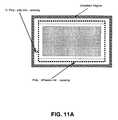
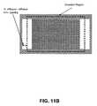
- FIG. 11Aillustrates an exemplary uncertain region of the polysilicon layer of the standard cell.
- Section IVdescribes exemplary parameters of a standard cell in a library.
- Section Vdescribes exemplary processes for using modified libraries in a mask correction process, such as an OPC process, and using modified libraries to design integrated circuits.
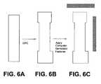
- Circuit layoutstypically undergoes a mask correction process (e.g., OPC) after the layout has been designed but before actual manufacturing.
- a mask correction processe.g., OPC
- the mask patterns for each layer of each cell in the layoutare corrected separately.
- original layout hierarchiesmay be altered and substantial flattening may occur during mask corrections.
- a conventional mask correction processis applied.
- an OPC processis applied to determine mask corrections to compensate for proximity effects within the layer of the cell.
- the exemplary process illustrated in FIG. 3may be applied.
- an implicit validation processis typically performed at the evaluation points to validate the mask corrections.
- FIG. 6Billustrates the modified cell after applying a conventional mask correction process (e.g., an OPC process) and a validation process.
- step 515may be skipped.
- a plurality of computer-generated features at least partially within the uncertain region of this layer of the cellis applied to determine any proximity effects which may partially invalidate the modifications made in the previous step.
- An uncertain regionis an area near the cell where features from neighboring cells, if located within the region, may affect the printing of the features of the cell. This region is “uncertain” because one does not yet know what those neighboring features will be.
- FIG. 6Cillustrates exemplary computer-generated features (i.e., the shaded rectangles) near the modified cell.
- the computer-generated featuresmay be generated using other library cells.
- other cells from the libraryare chosen and placed near the cell being processed according to placement rules.
- the features of those other cellscan be replicated within an uncertain region of the cell.
- different cell and placement combinationsmay be used as different sets of computer-generated features within the uncertain region of the cell.
- FIG. 18illustrates an exemplary cell A surrounded by other cells as its computer-generated features within its uncertain region.
- the cells used as neighboring cellsmay be the original cells or the modified cells.
- cells B, E, F, and Gare original cells of the library
- cells C′ and D′are modified cells of C, D, respectively, from the library.
- a performance metric valuemay be used to determine the processing quality of a previous mask modification technique (if any).
- performance metricmay include, without limitation, errors or mismatches between printed and intended image, image slopes or contrasts, mask error factors, dose and defocus latitudes, sensitivity to aberrations or flare, other metric, and/or a combination of the above.
- errorsor error values
- FIG. 5will use errors (or error values) as an exemplary performance metric.
- An error valuerepresents an amount of distortion caused by the computer-generated features (plus any remaining residual error from the OPC process of step 515 ) at a control point on the cell.
- FIG. 6Dillustrates an exemplary representation of error values determined after a validation process. In this Figure, the dotted lines represent the boundary of the simulated printed image after the validation process.
- Step 525an alternative process will now be described with reference to FIG. 19 .
- This alternative processshould be considered as an alternative implementation replacing steps 535 - 545 of FIG. 5 .
- step 1940whether enough sets of computer-generated features have been applied is determined. In an exemplary implementation, multiple sets of computer-generated features are used to obtain a more statistically significant quantitative analysis. If not enough sets have been applied, the process returns to step 520 and another set of computer-generated features at least partially within the uncertain region is applied to determine additional error values at the remaining control points of the cell.
- the remaining control pointsare determined to be valid or invalid at steps 1920 and 1930 to remove additional invalid control points from the total control points for the next iteration.
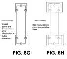
- segments containing or in close proximity to the invalid control pointsare determined. In an exemplary implementation, these segments are output as candidate areas.
- one or more polygonal areas encompassing the segmentsare mapped (or determined) as being the candidate areas that indicate portions of the cell that may require further processing.
- FIG. 9illustrates another exemplary process for mapping invalid control points to candidate areas on a cell.
- the parameters specified by the library for each cellcan be used to determine the uncertain regions for each layer of the cell.
- An uncertain region of a layer of a cellrepresents the area within which potential features from other cells may reside and cause proximity effects on the features within the cell.
- Oneis uncertain about the contents of the region because one does not necessarily have information regarding the actual layout of the cell's neighbors.
- each layerwill have its own uncertain region.
- the inner boundary of an uncertain regionis based on one or more parameters specified in the library for the cell and the outer boundary of the uncertain region is based on the interactive range for the cell.
- the computer-generated featuresi.e., at step 520 ) are applied within the uncertain region of each layer of a cell to determine any potential proximity effects that may be caused by the computer-generated features may have on the cell.
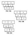
- FIG. 11Aillustrates the uncertain region for the placement style of FIG. 13A .
- the inner boundary of the uncertain regionwill be farther from the active cell border (i.e., by the diffusion power strip width plus the poly-diffusion minimum spacing and diffusion minimum spacing).
- the designerdesigns a physical layout using modified cells from the modified library.
- the embodiments described hereinmay be implemented in an operating environment comprising software installed on a computer, in hardware, or in a combination of software and hardware.
Landscapes
- Engineering & Computer Science (AREA)
- Computer Hardware Design (AREA)
- Physics & Mathematics (AREA)
- Theoretical Computer Science (AREA)
- Evolutionary Computation (AREA)
- Geometry (AREA)
- General Engineering & Computer Science (AREA)
- General Physics & Mathematics (AREA)
- Design And Manufacture Of Integrated Circuits (AREA)
Abstract
Description
Claims (10)
Priority Applications (2)
| Application Number | Priority Date | Filing Date | Title |
|---|---|---|---|
| US11/273,685US7934184B2 (en) | 2005-11-14 | 2005-11-14 | Integrated circuit design using modified cells |
| US13/066,832US20110209105A1 (en) | 2005-11-14 | 2011-04-25 | Photolithographic mask correction |
Applications Claiming Priority (1)
| Application Number | Priority Date | Filing Date | Title |
|---|---|---|---|
| US11/273,685US7934184B2 (en) | 2005-11-14 | 2005-11-14 | Integrated circuit design using modified cells |
Related Child Applications (1)
| Application Number | Title | Priority Date | Filing Date |
|---|---|---|---|
| US13/066,832DivisionUS20110209105A1 (en) | 2005-11-14 | 2011-04-25 | Photolithographic mask correction |
Publications (2)
| Publication Number | Publication Date |
|---|---|
| US20070113216A1 US20070113216A1 (en) | 2007-05-17 |
| US7934184B2true US7934184B2 (en) | 2011-04-26 |
Family
ID=38042412
Family Applications (2)
| Application Number | Title | Priority Date | Filing Date |
|---|---|---|---|
| US11/273,685Active2028-05-05US7934184B2 (en) | 2005-11-14 | 2005-11-14 | Integrated circuit design using modified cells |
| US13/066,832AbandonedUS20110209105A1 (en) | 2005-11-14 | 2011-04-25 | Photolithographic mask correction |
Family Applications After (1)
| Application Number | Title | Priority Date | Filing Date |
|---|---|---|---|
| US13/066,832AbandonedUS20110209105A1 (en) | 2005-11-14 | 2011-04-25 | Photolithographic mask correction |
Country Status (1)
| Country | Link |
|---|---|
| US (2) | US7934184B2 (en) |
Cited By (22)
| Publication number | Priority date | Publication date | Assignee | Title |
|---|---|---|---|---|
| US20110145775A1 (en)* | 2009-12-11 | 2011-06-16 | Kabushiki Kaisha Toshiba | Cell library, layout method, and layout apparatus |
| US8541879B2 (en) | 2007-12-13 | 2013-09-24 | Tela Innovations, Inc. | Super-self-aligned contacts and method for making the same |
| US8549455B2 (en) | 2007-08-02 | 2013-10-01 | Tela Innovations, Inc. | Methods for cell phasing and placement in dynamic array architecture and implementation of the same |
| US8552508B2 (en) | 2008-03-13 | 2013-10-08 | Tela Innovations, Inc. | Integrated circuit including cross-coupled transistors having gate electrodes formed within gate level feature layout channels with shared diffusion regions on opposite sides of two-transistor-forming gate level feature and electrical connection of transistor gates through linear interconnect conductors in single interconnect layer |
| US8653857B2 (en) | 2006-03-09 | 2014-02-18 | Tela Innovations, Inc. | Circuitry and layouts for XOR and XNOR logic |
| US8658542B2 (en) | 2006-03-09 | 2014-02-25 | Tela Innovations, Inc. | Coarse grid design methods and structures |
| US8661392B2 (en) | 2009-10-13 | 2014-02-25 | Tela Innovations, Inc. | Methods for cell boundary encroachment and layouts implementing the Same |
| US8667443B2 (en) | 2007-03-05 | 2014-03-04 | Tela Innovations, Inc. | Integrated circuit cell library for multiple patterning |
| US8680626B2 (en) | 2007-10-26 | 2014-03-25 | Tela Innovations, Inc. | Methods, structures, and designs for self-aligning local interconnects used in integrated circuits |
| US8701071B2 (en) | 2008-01-31 | 2014-04-15 | Tela Innovations, Inc. | Enforcement of semiconductor structure regularity for localized transistors and interconnect |
| US8756551B2 (en) | 2007-08-02 | 2014-06-17 | Tela Innovations, Inc. | Methods for designing semiconductor device with dynamic array section |
| US8759985B2 (en) | 2008-03-27 | 2014-06-24 | Tela Innovations, Inc. | Methods for multi-wire routing and apparatus implementing same |
| US8823062B2 (en) | 2006-03-09 | 2014-09-02 | Tela Innovations, Inc. | Integrated circuit with offset line end spacings in linear gate electrode level |
| US8839175B2 (en) | 2006-03-09 | 2014-09-16 | Tela Innovations, Inc. | Scalable meta-data objects |
| US8863063B2 (en) | 2009-05-06 | 2014-10-14 | Tela Innovations, Inc. | Finfet transistor circuit |
| US9035359B2 (en) | 2006-03-09 | 2015-05-19 | Tela Innovations, Inc. | Semiconductor chip including region including linear-shaped conductive structures forming gate electrodes and having electrical connection areas arranged relative to inner region between transistors of different types and associated methods |
| US9122832B2 (en) | 2008-08-01 | 2015-09-01 | Tela Innovations, Inc. | Methods for controlling microloading variation in semiconductor wafer layout and fabrication |
| US9159627B2 (en) | 2010-11-12 | 2015-10-13 | Tela Innovations, Inc. | Methods for linewidth modification and apparatus implementing the same |
| US9230910B2 (en) | 2006-03-09 | 2016-01-05 | Tela Innovations, Inc. | Oversized contacts and vias in layout defined by linearly constrained topology |
| US9563733B2 (en) | 2009-05-06 | 2017-02-07 | Tela Innovations, Inc. | Cell circuit and layout with linear finfet structures |
| US9754878B2 (en) | 2006-03-09 | 2017-09-05 | Tela Innovations, Inc. | Semiconductor chip including a chip level based on a layout that includes both regular and irregular wires |
| US11500283B2 (en) | 2019-09-03 | 2022-11-15 | Samsung Electronics Co., Ltd. | Mask layout correction method and a method for fabricating semiconductor devices using the same |
Families Citing this family (20)
| Publication number | Priority date | Publication date | Assignee | Title |
|---|---|---|---|---|
| US7694267B1 (en)* | 2006-02-03 | 2010-04-06 | Brion Technologies, Inc. | Method for process window optimized optical proximity correction |
| US8245180B2 (en) | 2006-03-09 | 2012-08-14 | Tela Innovations, Inc. | Methods for defining and using co-optimized nanopatterns for integrated circuit design and apparatus implementing same |
| US7943967B2 (en) | 2006-03-09 | 2011-05-17 | Tela Innovations, Inc. | Semiconductor device and associated layouts including diffusion contact placement restriction based on relation to linear conductive segments |
| US8225261B2 (en) | 2006-03-09 | 2012-07-17 | Tela Innovations, Inc. | Methods for defining contact grid in dynamic array architecture |
| US7932545B2 (en)* | 2006-03-09 | 2011-04-26 | Tela Innovations, Inc. | Semiconductor device and associated layouts including gate electrode level region having arrangement of six linear conductive segments with side-to-side spacing less than 360 nanometers |
| US8247846B2 (en) | 2006-03-09 | 2012-08-21 | Tela Innovations, Inc. | Oversized contacts and vias in semiconductor chip defined by linearly constrained topology |
| US8225239B2 (en) | 2006-03-09 | 2012-07-17 | Tela Innovations, Inc. | Methods for defining and utilizing sub-resolution features in linear topology |
| US7496862B2 (en)* | 2006-08-29 | 2009-02-24 | Taiwan Semiconductor Manufacturing Co., Ltd. | Method for automatically modifying integrated circuit layout |
| US8286107B2 (en)* | 2007-02-20 | 2012-10-09 | Tela Innovations, Inc. | Methods and systems for process compensation technique acceleration |
| US7979829B2 (en)* | 2007-02-20 | 2011-07-12 | Tela Innovations, Inc. | Integrated circuit cell library with cell-level process compensation technique (PCT) application and associated methods |
| US7562326B2 (en)* | 2007-08-09 | 2009-07-14 | United Microelectronics Corp. | Method of generating a standard cell layout and transferring the standard cell layout to a substrate |
| JP2010177374A (en)* | 2009-01-28 | 2010-08-12 | Toshiba Corp | Pattern verifying method and method for manufacturing semiconductor device |
| US8619236B2 (en)* | 2010-11-24 | 2013-12-31 | International Business Machines Corporation | Determining lithographic set point using optical proximity correction verification simulation |
| US8577489B2 (en) | 2011-01-26 | 2013-11-05 | International Business Machines Corporation | Diagnosing in-line critical dimension control adjustments using optical proximity correction verification |
| US8499260B2 (en) | 2011-01-26 | 2013-07-30 | International Business Machines Corporation | Optical proximity correction verification accounting for mask deviations |
| US8719756B2 (en)* | 2011-10-06 | 2014-05-06 | Oracle International Corporation | Power grid mosaicing with deep-sub-tile cells |
| US8826195B2 (en) | 2012-06-05 | 2014-09-02 | Taiwan Semiconductor Manufacturing Co., Ltd. | Layout modification method and system |
| US9230049B1 (en) | 2014-09-05 | 2016-01-05 | Oracle International Corporation | Arraying power grid vias by tile cells |
| US10380307B1 (en)* | 2016-03-30 | 2019-08-13 | Silicon Technologies, Inc. | Analog design tool, cell set, and related methods, systems and equipment |
| US10192018B1 (en)* | 2016-03-31 | 2019-01-29 | Cadence Design Systems, Inc. | Method and system for implementing efficient trim data representation for an electronic design |
Citations (23)
| Publication number | Priority date | Publication date | Assignee | Title |
|---|---|---|---|---|
| US5242770A (en) | 1992-01-16 | 1993-09-07 | Microunity Systems Engineering, Inc. | Mask for photolithography |
| US5447810A (en) | 1994-02-09 | 1995-09-05 | Microunity Systems Engineering, Inc. | Masks for improved lithographic patterning for off-axis illumination lithography |
| US5858580A (en) | 1997-09-17 | 1999-01-12 | Numerical Technologies, Inc. | Phase shifting circuit manufacture method and apparatus |
| US5978501A (en)* | 1997-01-03 | 1999-11-02 | International Business Machines Corporation | Adaptive inspection method and system |
| US6194252B1 (en)* | 1996-07-15 | 2001-02-27 | Kabushiki Kaisha Toshiba | Semiconductor device and manufacturing method for the same, basic cell library and manufacturing method for the same, and mask |
| US6289499B1 (en) | 1997-12-31 | 2001-09-11 | Avant! Corporation | Proximity correction software for wafer lithography |
| US6335130B1 (en) | 2000-05-01 | 2002-01-01 | Asml Masktools Netherlands B.V. | System and method of providing optical proximity correction for features using phase-shifted halftone transparent/semi-transparent features |
| US6425117B1 (en)* | 1995-03-06 | 2002-07-23 | Lsi Logic Corporation | System and method for performing optical proximity correction on the interface between optical proximity corrected cells |
| US6430737B1 (en) | 2000-07-10 | 2002-08-06 | Mentor Graphics Corp. | Convergence technique for model-based optical and process correction |
| US6505327B2 (en) | 2001-04-13 | 2003-01-07 | Numerical Technologies, Inc. | Generating an instance-based representation of a design hierarchy |
| US6507931B2 (en) | 2000-06-30 | 2003-01-14 | Kabushiki Kaisha Toshiba | Semiconductor integrated circuit designing method and system |
| US6668367B2 (en) | 2002-01-24 | 2003-12-23 | Nicolas B. Cobb | Selective promotion for resolution enhancement techniques |
| US6763514B2 (en) | 2001-12-12 | 2004-07-13 | Numerical Technologies, Inc. | Method and apparatus for controlling rippling during optical proximity correction |
| US20040205688A1 (en) | 2003-04-14 | 2004-10-14 | Fortis Systems, Inc. | Effective proximity effect correction methodology |
| US6807663B2 (en)* | 2002-09-23 | 2004-10-19 | Numerical Technologies, Inc. | Accelerated layout processing using OPC pre-processing |
| US6813758B2 (en) | 2002-03-14 | 2004-11-02 | Lsi Logic Corporation | Optical proximity correction driven hierarchy |
| US20050193363A1 (en)* | 2004-02-26 | 2005-09-01 | Puneet Gupta | Method of IC fabrication, IC mask fabrication and program product therefor |
| US6964031B2 (en)* | 2001-09-29 | 2005-11-08 | Kabushiki Kaisha Toshiba | Mask pattern generating method and manufacturing method of semiconductor apparatus |
| US7103870B2 (en)* | 1999-03-04 | 2006-09-05 | Matsushita Electric Industrial Co., Ltd. | Method for planning layout for LSI pattern, method for forming LSI pattern and method for generating mask data for LSI |
| US20070124718A1 (en)* | 2005-05-25 | 2007-05-31 | Sachiko Kobayashi | Mask manufacturing system, mask data creating method and manufacturing method of semiconductor device |
| US7263683B1 (en)* | 2004-09-07 | 2007-08-28 | Advanced Micro Devices, Inc. | Simplified optical proximity correction based on 1-dimension versus 2-dimension pattern shape classification |
| US20090182448A1 (en)* | 2008-01-16 | 2009-07-16 | International Business Machines Corporation | Method to check model accuracy during wafer patterning simulation |
| US7627837B2 (en)* | 2004-10-15 | 2009-12-01 | Takumi Technology Corp. | Model-based pattern characterization to generate rules for rule-model-based hybrid optical proximity correction |
Family Cites Families (5)
| Publication number | Priority date | Publication date | Assignee | Title |
|---|---|---|---|---|
| US6425113B1 (en)* | 2000-06-13 | 2002-07-23 | Leigh C. Anderson | Integrated verification and manufacturability tool |
| JP4592438B2 (en)* | 2005-02-08 | 2010-12-01 | 株式会社東芝 | Semiconductor integrated circuit layout method, manufacturing method, and layout program |
| JP2007080965A (en)* | 2005-09-12 | 2007-03-29 | Matsushita Electric Ind Co Ltd | Semiconductor device manufacturing method, library used therefor, recording medium, and semiconductor manufacturing apparatus |
| US7747977B1 (en)* | 2005-09-15 | 2010-06-29 | D2S, Inc. | Method and system for stencil design for particle beam writing |
| WO2007038972A1 (en)* | 2005-09-20 | 2007-04-12 | Freescale Semiconductor, Inc. | Method of making an integrated circuit |
- 2005
- 2005-11-14USUS11/273,685patent/US7934184B2/enactiveActive
- 2011
- 2011-04-25USUS13/066,832patent/US20110209105A1/ennot_activeAbandoned
Patent Citations (24)
| Publication number | Priority date | Publication date | Assignee | Title |
|---|---|---|---|---|
| US5242770A (en) | 1992-01-16 | 1993-09-07 | Microunity Systems Engineering, Inc. | Mask for photolithography |
| US5447810A (en) | 1994-02-09 | 1995-09-05 | Microunity Systems Engineering, Inc. | Masks for improved lithographic patterning for off-axis illumination lithography |
| US6425117B1 (en)* | 1995-03-06 | 2002-07-23 | Lsi Logic Corporation | System and method for performing optical proximity correction on the interface between optical proximity corrected cells |
| US6194252B1 (en)* | 1996-07-15 | 2001-02-27 | Kabushiki Kaisha Toshiba | Semiconductor device and manufacturing method for the same, basic cell library and manufacturing method for the same, and mask |
| US5978501A (en)* | 1997-01-03 | 1999-11-02 | International Business Machines Corporation | Adaptive inspection method and system |
| US5858580A (en) | 1997-09-17 | 1999-01-12 | Numerical Technologies, Inc. | Phase shifting circuit manufacture method and apparatus |
| US6289499B1 (en) | 1997-12-31 | 2001-09-11 | Avant! Corporation | Proximity correction software for wafer lithography |
| US7103870B2 (en)* | 1999-03-04 | 2006-09-05 | Matsushita Electric Industrial Co., Ltd. | Method for planning layout for LSI pattern, method for forming LSI pattern and method for generating mask data for LSI |
| US6335130B1 (en) | 2000-05-01 | 2002-01-01 | Asml Masktools Netherlands B.V. | System and method of providing optical proximity correction for features using phase-shifted halftone transparent/semi-transparent features |
| US6507931B2 (en) | 2000-06-30 | 2003-01-14 | Kabushiki Kaisha Toshiba | Semiconductor integrated circuit designing method and system |
| US6430737B1 (en) | 2000-07-10 | 2002-08-06 | Mentor Graphics Corp. | Convergence technique for model-based optical and process correction |
| US6505327B2 (en) | 2001-04-13 | 2003-01-07 | Numerical Technologies, Inc. | Generating an instance-based representation of a design hierarchy |
| US6964031B2 (en)* | 2001-09-29 | 2005-11-08 | Kabushiki Kaisha Toshiba | Mask pattern generating method and manufacturing method of semiconductor apparatus |
| US6763514B2 (en) | 2001-12-12 | 2004-07-13 | Numerical Technologies, Inc. | Method and apparatus for controlling rippling during optical proximity correction |
| US6668367B2 (en) | 2002-01-24 | 2003-12-23 | Nicolas B. Cobb | Selective promotion for resolution enhancement techniques |
| US6813758B2 (en) | 2002-03-14 | 2004-11-02 | Lsi Logic Corporation | Optical proximity correction driven hierarchy |
| US6807663B2 (en)* | 2002-09-23 | 2004-10-19 | Numerical Technologies, Inc. | Accelerated layout processing using OPC pre-processing |
| US20040205688A1 (en) | 2003-04-14 | 2004-10-14 | Fortis Systems, Inc. | Effective proximity effect correction methodology |
| US20050193363A1 (en)* | 2004-02-26 | 2005-09-01 | Puneet Gupta | Method of IC fabrication, IC mask fabrication and program product therefor |
| US7263683B1 (en)* | 2004-09-07 | 2007-08-28 | Advanced Micro Devices, Inc. | Simplified optical proximity correction based on 1-dimension versus 2-dimension pattern shape classification |
| US7627837B2 (en)* | 2004-10-15 | 2009-12-01 | Takumi Technology Corp. | Model-based pattern characterization to generate rules for rule-model-based hybrid optical proximity correction |
| US20100153904A1 (en)* | 2004-10-15 | 2010-06-17 | Youping Zhang | Model-based pattern characterization to generate rules for rule-model-based hybrid optical proximity correction |
| US20070124718A1 (en)* | 2005-05-25 | 2007-05-31 | Sachiko Kobayashi | Mask manufacturing system, mask data creating method and manufacturing method of semiconductor device |
| US20090182448A1 (en)* | 2008-01-16 | 2009-07-16 | International Business Machines Corporation | Method to check model accuracy during wafer patterning simulation |
Non-Patent Citations (1)
| Title |
|---|
| Rieger et al., "Using Behavior Modelling for Proximity Correction," SPIE 1994. |
Cited By (106)
| Publication number | Priority date | Publication date | Assignee | Title |
|---|---|---|---|---|
| US8823062B2 (en) | 2006-03-09 | 2014-09-02 | Tela Innovations, Inc. | Integrated circuit with offset line end spacings in linear gate electrode level |
| US10230377B2 (en) | 2006-03-09 | 2019-03-12 | Tela Innovations, Inc. | Circuitry and layouts for XOR and XNOR logic |
| US10217763B2 (en) | 2006-03-09 | 2019-02-26 | Tela Innovations, Inc. | Semiconductor chip having region including gate electrode features of rectangular shape on gate horizontal grid and first-metal structures of rectangular shape on at least eight first-metal gridlines of first-metal vertical grid |
| US10186523B2 (en) | 2006-03-09 | 2019-01-22 | Tela Innovations, Inc. | Semiconductor chip having region including gate electrode features formed in part from rectangular layout shapes on gate horizontal grid and first-metal structures formed in part from rectangular layout shapes on at least eight first-metal gridlines of first-metal vertical grid |
| US10141334B2 (en) | 2006-03-09 | 2018-11-27 | Tela Innovations, Inc. | Semiconductor chip including region having rectangular-shaped gate structures and first-metal structures |
| US10141335B2 (en) | 2006-03-09 | 2018-11-27 | Tela Innovations, Inc. | Semiconductor CIP including region having rectangular-shaped gate structures and first metal structures |
| US9917056B2 (en) | 2006-03-09 | 2018-03-13 | Tela Innovations, Inc. | Coarse grid design methods and structures |
| US9905576B2 (en) | 2006-03-09 | 2018-02-27 | Tela Innovations, Inc. | Semiconductor chip including region having rectangular-shaped gate structures and first metal structures |
| US9859277B2 (en) | 2006-03-09 | 2018-01-02 | Tela Innovations, Inc. | Methods, structures, and designs for self-aligning local interconnects used in integrated circuits |
| US9754878B2 (en) | 2006-03-09 | 2017-09-05 | Tela Innovations, Inc. | Semiconductor chip including a chip level based on a layout that includes both regular and irregular wires |
| US9741719B2 (en) | 2006-03-09 | 2017-08-22 | Tela Innovations, Inc. | Methods, structures, and designs for self-aligning local interconnects used in integrated circuits |
| US9711495B2 (en) | 2006-03-09 | 2017-07-18 | Tela Innovations, Inc. | Oversized contacts and vias in layout defined by linearly constrained topology |
| US9673825B2 (en) | 2006-03-09 | 2017-06-06 | Tela Innovations, Inc. | Circuitry and layouts for XOR and XNOR logic |
| US8653857B2 (en) | 2006-03-09 | 2014-02-18 | Tela Innovations, Inc. | Circuitry and layouts for XOR and XNOR logic |
| US8658542B2 (en) | 2006-03-09 | 2014-02-25 | Tela Innovations, Inc. | Coarse grid design methods and structures |
| US9589091B2 (en) | 2006-03-09 | 2017-03-07 | Tela Innovations, Inc. | Scalable meta-data objects |
| US9443947B2 (en) | 2006-03-09 | 2016-09-13 | Tela Innovations, Inc. | Semiconductor chip including region having integrated circuit transistor gate electrodes formed by various conductive structures of specified shape and position and method for manufacturing the same |
| US9425272B2 (en) | 2006-03-09 | 2016-08-23 | Tela Innovations, Inc. | Semiconductor chip including integrated circuit including four transistors of first transistor type and four transistors of second transistor type with electrical connections between various transistors and methods for manufacturing the same |
| US9425273B2 (en) | 2006-03-09 | 2016-08-23 | Tela Innovations, Inc. | Semiconductor chip including integrated circuit including at least five gate level conductive structures having particular spatial and electrical relationship and method for manufacturing the same |
| US9425145B2 (en) | 2006-03-09 | 2016-08-23 | Tela Innovations, Inc. | Oversized contacts and vias in layout defined by linearly constrained topology |
| US9336344B2 (en) | 2006-03-09 | 2016-05-10 | Tela Innovations, Inc. | Coarse grid design methods and structures |
| US9240413B2 (en) | 2006-03-09 | 2016-01-19 | Tela Innovations, Inc. | Methods, structures, and designs for self-aligning local interconnects used in integrated circuits |
| US9230910B2 (en) | 2006-03-09 | 2016-01-05 | Tela Innovations, Inc. | Oversized contacts and vias in layout defined by linearly constrained topology |
| US9035359B2 (en) | 2006-03-09 | 2015-05-19 | Tela Innovations, Inc. | Semiconductor chip including region including linear-shaped conductive structures forming gate electrodes and having electrical connection areas arranged relative to inner region between transistors of different types and associated methods |
| US9009641B2 (en) | 2006-03-09 | 2015-04-14 | Tela Innovations, Inc. | Circuits with linear finfet structures |
| US8952425B2 (en) | 2006-03-09 | 2015-02-10 | Tela Innovations, Inc. | Integrated circuit including at least four linear-shaped conductive structures having extending portions of different length |
| US8946781B2 (en) | 2006-03-09 | 2015-02-03 | Tela Innovations, Inc. | Integrated circuit including gate electrode conductive structures with different extension distances beyond contact |
| US8921896B2 (en) | 2006-03-09 | 2014-12-30 | Tela Innovations, Inc. | Integrated circuit including linear gate electrode structures having different extension distances beyond contact |
| US8921897B2 (en) | 2006-03-09 | 2014-12-30 | Tela Innovations, Inc. | Integrated circuit with gate electrode conductive structures having offset ends |
| US8839175B2 (en) | 2006-03-09 | 2014-09-16 | Tela Innovations, Inc. | Scalable meta-data objects |
| US9633987B2 (en) | 2007-03-05 | 2017-04-25 | Tela Innovations, Inc. | Integrated circuit cell library for multiple patterning |
| US10074640B2 (en) | 2007-03-05 | 2018-09-11 | Tela Innovations, Inc. | Integrated circuit cell library for multiple patterning |
| US8667443B2 (en) | 2007-03-05 | 2014-03-04 | Tela Innovations, Inc. | Integrated circuit cell library for multiple patterning |
| US9595515B2 (en) | 2007-03-07 | 2017-03-14 | Tela Innovations, Inc. | Semiconductor chip including integrated circuit defined within dynamic array section |
| US9424387B2 (en) | 2007-03-07 | 2016-08-23 | Tela Innovations, Inc. | Methods for cell phasing and placement in dynamic array architecture and implementation of the same |
| US8966424B2 (en) | 2007-03-07 | 2015-02-24 | Tela Innovations, Inc. | Methods for cell phasing and placement in dynamic array architecture and implementation of the same |
| US9910950B2 (en) | 2007-03-07 | 2018-03-06 | Tela Innovations, Inc. | Methods for cell phasing and placement in dynamic array architecture and implementation of the same |
| US8756551B2 (en) | 2007-08-02 | 2014-06-17 | Tela Innovations, Inc. | Methods for designing semiconductor device with dynamic array section |
| US8759882B2 (en) | 2007-08-02 | 2014-06-24 | Tela Innovations, Inc. | Semiconductor device with dynamic array sections defined and placed according to manufacturing assurance halos |
| US8549455B2 (en) | 2007-08-02 | 2013-10-01 | Tela Innovations, Inc. | Methods for cell phasing and placement in dynamic array architecture and implementation of the same |
| US8680626B2 (en) | 2007-10-26 | 2014-03-25 | Tela Innovations, Inc. | Methods, structures, and designs for self-aligning local interconnects used in integrated circuits |
| US10734383B2 (en) | 2007-10-26 | 2020-08-04 | Tela Innovations, Inc. | Methods, structures, and designs for self-aligning local interconnects used in integrated circuits |
| US9818747B2 (en) | 2007-12-13 | 2017-11-14 | Tela Innovations, Inc. | Super-self-aligned contacts and method for making the same |
| US8541879B2 (en) | 2007-12-13 | 2013-09-24 | Tela Innovations, Inc. | Super-self-aligned contacts and method for making the same |
| US10461081B2 (en) | 2007-12-13 | 2019-10-29 | Tel Innovations, Inc. | Super-self-aligned contacts and method for making the same |
| US9281371B2 (en) | 2007-12-13 | 2016-03-08 | Tela Innovations, Inc. | Super-self-aligned contacts and method for making the same |
| US8951916B2 (en) | 2007-12-13 | 2015-02-10 | Tela Innovations, Inc. | Super-self-aligned contacts and method for making the same |
| US9530734B2 (en) | 2008-01-31 | 2016-12-27 | Tela Innovations, Inc. | Enforcement of semiconductor structure regularity for localized transistors and interconnect |
| US8701071B2 (en) | 2008-01-31 | 2014-04-15 | Tela Innovations, Inc. | Enforcement of semiconductor structure regularity for localized transistors and interconnect |
| US9202779B2 (en) | 2008-01-31 | 2015-12-01 | Tela Innovations, Inc. | Enforcement of semiconductor structure regularity for localized transistors and interconnect |
| US8680583B2 (en) | 2008-03-13 | 2014-03-25 | Tela Innovations, Inc. | Integrated circuit including cross-coupled transistors having gate electrodes formed within at least nine gate level feature layout channels |
| US8836045B2 (en) | 2008-03-13 | 2014-09-16 | Tela Innovations, Inc. | Cross-coupled transistor circuit having diffusion regions of common node on opposing sides of same gate electrode track |
| US8735944B2 (en) | 2008-03-13 | 2014-05-27 | Tela Innovations, Inc. | Integrated circuit including cross-coupled transistors having gate electrodes formed within gate level feature layout channels with serially connected transistors |
| US8729643B2 (en) | 2008-03-13 | 2014-05-20 | Tela Innovations, Inc. | Cross-coupled transistor circuit including offset inner gate contacts |
| US9081931B2 (en) | 2008-03-13 | 2015-07-14 | Tela Innovations, Inc. | Cross-coupled transistor circuit having diffusion regions of common node on opposing sides of same gate electrode track and gate node connection through single interconnect layer |
| US9117050B2 (en) | 2008-03-13 | 2015-08-25 | Tela Innovations, Inc. | Integrated circuit including cross-coupled transistors having gate electrodes formed within gate level feature layout channels with gate contact position and offset specifications |
| US8785979B2 (en) | 2008-03-13 | 2014-07-22 | Tela Innovations, Inc. | Integrated circuit including cross-coupled transistors having gate electrodes formed within gate level feature layout channels with two inside positioned gate contacts and two outside positioned gate contacts and electrical connection of cross-coupled transistors through same interconnect layer |
| US10727252B2 (en) | 2008-03-13 | 2020-07-28 | Tela Innovations, Inc. | Semiconductor chip including integrated circuit having cross-coupled transistor configuration and method for manufacturing the same |
| US8742463B2 (en) | 2008-03-13 | 2014-06-03 | Tela Innovations, Inc. | Integrated circuit including cross-coupled transistors having gate electrodes formed within gate level feature layout channels with outer positioned gate contacts |
| US9208279B2 (en) | 2008-03-13 | 2015-12-08 | Tela Innovations, Inc. | Semiconductor chip including digital logic circuit including linear-shaped conductive structures having electrical connection areas located within inner region between transistors of different type and associated methods |
| US9213792B2 (en) | 2008-03-13 | 2015-12-15 | Tela Innovations, Inc. | Semiconductor chip including digital logic circuit including at least six transistors with some transistors forming cross-coupled transistor configuration and associated methods |
| US8729606B2 (en) | 2008-03-13 | 2014-05-20 | Tela Innovations, Inc. | Integrated circuit including cross-coupled transistors having gate electrodes formed within gate level feature layout channels |
| US8742462B2 (en) | 2008-03-13 | 2014-06-03 | Tela Innovations, Inc. | Integrated circuit including cross-coupled transistors having gate electrodes formed within gate level feature layout channels with gate contact position specifications |
| US9245081B2 (en) | 2008-03-13 | 2016-01-26 | Tela Innovations, Inc. | Semiconductor chip including digital logic circuit including at least nine linear-shaped conductive structures collectively forming gate electrodes of at least six transistors with some transistors forming cross-coupled transistor configuration and associated methods |
| US10658385B2 (en) | 2008-03-13 | 2020-05-19 | Tela Innovations, Inc. | Cross-coupled transistor circuit defined on four gate electrode tracks |
| US8872283B2 (en) | 2008-03-13 | 2014-10-28 | Tela Innovations, Inc. | Integrated circuit including cross-coupled transistors having gate electrodes formed within gate level feature layout channels with shared diffusion regions on opposite sides of two-transistor-forming gate level feature |
| US8772839B2 (en) | 2008-03-13 | 2014-07-08 | Tela Innovations, Inc. | Integrated circuit including cross-coupled transistors having gate electrodes formed within gate level feature layout channels with four inside positioned gate contacts having offset and aligned relationships and electrical connection of transistor gates through linear interconnect conductors in single interconnect layer |
| US10651200B2 (en) | 2008-03-13 | 2020-05-12 | Tela Innovations, Inc. | Cross-coupled transistor circuit defined on three gate electrode tracks |
| US8866197B2 (en) | 2008-03-13 | 2014-10-21 | Tela Innovations, Inc. | Integrated circuit including cross-coupled transistors having gate electrodes formed within gate level feature layout channels with at least two gate electrodes electrically connected to each other through another transistor forming gate level feature |
| US8785978B2 (en) | 2008-03-13 | 2014-07-22 | Tela Innovations, Inc. | Integrated circuit including cross-coupled transistors having gate electrodes formed within gate level feature layout channels with electrical connection of cross-coupled transistors through same interconnect layer |
| US8669595B2 (en) | 2008-03-13 | 2014-03-11 | Tela Innovations, Inc. | Integrated circuit including cross-coupled transistors having gate electrodes formed within gate level feature layout channels with gate contact position, alignment, and offset specifications |
| US8669594B2 (en) | 2008-03-13 | 2014-03-11 | Tela Innovations, Inc. | Integrated circuit including cross-coupled transistors having gate electrodes formed within at least twelve gate level feature layout channels |
| US8853793B2 (en) | 2008-03-13 | 2014-10-07 | Tela Innovations, Inc. | Integrated circuit including gate electrode level region including cross-coupled transistors having gate contacts located over inner portion of gate electrode level region and offset gate level feature line ends |
| US8853794B2 (en) | 2008-03-13 | 2014-10-07 | Tela Innovations, Inc. | Integrated circuit within semiconductor chip including cross-coupled transistor configuration |
| US8816402B2 (en) | 2008-03-13 | 2014-08-26 | Tela Innovations, Inc. | Integrated circuit including cross-coupled transistors having gate electrodes formed within gate level feature layout channels with gate level feature layout channel including single transistor |
| US9536899B2 (en) | 2008-03-13 | 2017-01-03 | Tela Innovations, Inc. | Semiconductor chip including integrated circuit having cross-coupled transistor configuration and method for manufacturing the same |
| US8552508B2 (en) | 2008-03-13 | 2013-10-08 | Tela Innovations, Inc. | Integrated circuit including cross-coupled transistors having gate electrodes formed within gate level feature layout channels with shared diffusion regions on opposite sides of two-transistor-forming gate level feature and electrical connection of transistor gates through linear interconnect conductors in single interconnect layer |
| US8552509B2 (en) | 2008-03-13 | 2013-10-08 | Tela Innovations, Inc. | Integrated circuit including cross-coupled transistors having gate electrodes formed within gate level feature layout channels with other transistors positioned between cross-coupled transistors |
| US8847329B2 (en) | 2008-03-13 | 2014-09-30 | Tela Innovations, Inc. | Cross-coupled transistor circuit defined having diffusion regions of common node on opposing sides of same gate electrode track with at least two non-inner positioned gate contacts |
| US8558322B2 (en) | 2008-03-13 | 2013-10-15 | Tela Innovations, Inc. | Integrated circuit including cross-coupled transistors having gate electrodes formed within gate level feature layout channels with at least two gate electrodes electrically connected to each other through gate level feature |
| US8592872B2 (en) | 2008-03-13 | 2013-11-26 | Tela Innovations, Inc. | Integrated circuit including cross-coupled transistors with two transistors of different type having gate electrodes formed by common gate level feature with shared diffusion regions on opposite sides of common gate level feature |
| US8835989B2 (en) | 2008-03-13 | 2014-09-16 | Tela Innovations, Inc. | Integrated circuit including cross-coupled transistors having gate electrodes formed within gate level feature layout channels with gate electrode placement specifications |
| US8587034B2 (en) | 2008-03-13 | 2013-11-19 | Tela Innovations, Inc. | Integrated circuit including cross-coupled transistors having gate electrodes formed within gate level feature layout channels with four inside positioned gate contacts and electrical connection of transistor gates through linear interconnect conductors in single interconnect layer |
| US8581303B2 (en) | 2008-03-13 | 2013-11-12 | Tela Innovations, Inc. | Integrated circuit including cross-coupled trasistors having gate electrodes formed within gate level feature layout channels with four inside positioned gate contacts having offset relationships and electrical connection of cross-coupled transistors through same interconnect layer |
| US8581304B2 (en) | 2008-03-13 | 2013-11-12 | Tela Innovations, Inc. | Integrated circuit including cross-coupled transistors having gate electrodes formed within gate level feature layout channels with four inside positioned gate contacts having offset and aligned relationships |
| US10020321B2 (en) | 2008-03-13 | 2018-07-10 | Tela Innovations, Inc. | Cross-coupled transistor circuit defined on two gate electrode tracks |
| US8847331B2 (en) | 2008-03-13 | 2014-09-30 | Tela Innovations, Inc. | Semiconductor chip including region having cross-coupled transistor configuration with offset electrical connection areas on gate electrode forming conductive structures and at least two different inner extension distances of gate electrode forming conductive structures |
| US8575706B2 (en) | 2008-03-13 | 2013-11-05 | Tela Innovations, Inc. | Integrated circuit including cross-coupled transistors having gate electrodes formed within gate level feature layout channels with at least two different gate level features inner extensions beyond gate electrode |
| US9871056B2 (en) | 2008-03-13 | 2018-01-16 | Tela Innovations, Inc. | Semiconductor chip including integrated circuit having cross-coupled transistor configuration and method for manufacturing the same |
| US8569841B2 (en) | 2008-03-13 | 2013-10-29 | Tela Innovations, Inc. | Integrated circuit including cross-coupled transistors having gate electrodes formed within gate level feature layout channels with at least one gate level feature extending into adjacent gate level feature layout channel |
| US8735995B2 (en) | 2008-03-13 | 2014-05-27 | Tela Innovations, Inc. | Cross-coupled transistor circuit defined on three gate electrode tracks with diffusion regions of common node on opposing sides of same gate electrode track |
| US8564071B2 (en) | 2008-03-13 | 2013-10-22 | Tela Innovations, Inc. | Integrated circuit including cross-coupled transistors having gate electrodes formed within gate level feature layout channels with at least two different gate level feature extensions beyond contact |
| US9390215B2 (en) | 2008-03-27 | 2016-07-12 | Tela Innovations, Inc. | Methods for multi-wire routing and apparatus implementing same |
| US9779200B2 (en) | 2008-03-27 | 2017-10-03 | Tela Innovations, Inc. | Methods for multi-wire routing and apparatus implementing same |
| US8759985B2 (en) | 2008-03-27 | 2014-06-24 | Tela Innovations, Inc. | Methods for multi-wire routing and apparatus implementing same |
| US9122832B2 (en) | 2008-08-01 | 2015-09-01 | Tela Innovations, Inc. | Methods for controlling microloading variation in semiconductor wafer layout and fabrication |
| US10446536B2 (en) | 2009-05-06 | 2019-10-15 | Tela Innovations, Inc. | Cell circuit and layout with linear finfet structures |
| US9563733B2 (en) | 2009-05-06 | 2017-02-07 | Tela Innovations, Inc. | Cell circuit and layout with linear finfet structures |
| US8863063B2 (en) | 2009-05-06 | 2014-10-14 | Tela Innovations, Inc. | Finfet transistor circuit |
| US8661392B2 (en) | 2009-10-13 | 2014-02-25 | Tela Innovations, Inc. | Methods for cell boundary encroachment and layouts implementing the Same |
| US9530795B2 (en) | 2009-10-13 | 2016-12-27 | Tela Innovations, Inc. | Methods for cell boundary encroachment and semiconductor devices implementing the same |
| US9269702B2 (en) | 2009-10-13 | 2016-02-23 | Tela Innovations, Inc. | Methods for cell boundary encroachment and layouts implementing the same |
| US20110145775A1 (en)* | 2009-12-11 | 2011-06-16 | Kabushiki Kaisha Toshiba | Cell library, layout method, and layout apparatus |
| US9159627B2 (en) | 2010-11-12 | 2015-10-13 | Tela Innovations, Inc. | Methods for linewidth modification and apparatus implementing the same |
| US9704845B2 (en) | 2010-11-12 | 2017-07-11 | Tela Innovations, Inc. | Methods for linewidth modification and apparatus implementing the same |
| US11500283B2 (en) | 2019-09-03 | 2022-11-15 | Samsung Electronics Co., Ltd. | Mask layout correction method and a method for fabricating semiconductor devices using the same |
Also Published As
| Publication number | Publication date |
|---|---|
| US20110209105A1 (en) | 2011-08-25 |
| US20070113216A1 (en) | 2007-05-17 |
Similar Documents
| Publication | Publication Date | Title |
|---|---|---|
| US7934184B2 (en) | Integrated circuit design using modified cells | |
| US11797746B2 (en) | Method of forming semiconductor device having more similar cell densities in alternating rows | |
| US7627837B2 (en) | Model-based pattern characterization to generate rules for rule-model-based hybrid optical proximity correction | |
| US5682323A (en) | System and method for performing optical proximity correction on macrocell libraries | |
| US7337421B2 (en) | Method and system for managing design corrections for optical and process effects based on feature tolerances | |
| Otto et al. | Automated optical proximity correction: a rules-based approach | |
| US7001693B2 (en) | Binary OPC for assist feature layout optimization | |
| KR101096145B1 (en) | Methods of Performing Model-Based Lithography Guided Layout Design | |
| US7172838B2 (en) | Chromeless phase mask layout generation | |
| US5900340A (en) | One dimensional lithographic proximity correction using DRC shape functions | |
| US7945871B2 (en) | Integrated OPC verification tool | |
| US7814456B2 (en) | Method and system for topography-aware reticle enhancement | |
| CN111048505A (en) | Semiconductor device and method and system for manufacturing the same | |
| US20030192013A1 (en) | Method and apparatus for facilitating process-compliant layout optimization | |
| JP4395047B2 (en) | Renesting into designs for efficient long-range calculation of correlation maps | |
| US20120042291A1 (en) | Inverse Mask Design and Correction for Electronic Design | |
| US20100162194A1 (en) | Method for Selectively Enlarging Via and Contact Sizes | |
| US9754068B2 (en) | Method, computer readable storage medium and computer system for creating a layout of a photomask | |
| KR102570888B1 (en) | Method for correcting a mask layout and method of fabricating a semiconductor device using the same | |
| JP6108693B2 (en) | Pattern creation method | |
| US9779186B2 (en) | Methods for performing model-based lithography guided layout design | |
| US20100081294A1 (en) | Pattern data creating method, pattern data creating program, and semiconductor device manufacturing method | |
| US12230318B2 (en) | Memory device including a word line with portions with different sizes in different metal layers | |
| US9875334B2 (en) | Generating manufacturable sub-resolution assist feature shapes from a usefulness map | |
| KR20230116422A (en) | Method for fabricating phtomask layout and method for fabricating of semiconductor device using the same |
Legal Events
| Date | Code | Title | Description |
|---|---|---|---|
| AS | Assignment | Owner name:TAKUMI TECHNOLOGY CORPORATION,CALIFORNIA Free format text:ASSIGNMENT OF ASSIGNORS INTEREST;ASSIGNOR:ZHANG, YOUPING;REEL/FRAME:017244/0493 Effective date:20051028 Owner name:TAKUMI TECHNOLOGY CORPORATION, CALIFORNIA Free format text:ASSIGNMENT OF ASSIGNORS INTEREST;ASSIGNOR:ZHANG, YOUPING;REEL/FRAME:017244/0493 Effective date:20051028 | |
| STCF | Information on status: patent grant | Free format text:PATENTED CASE | |
| REMI | Maintenance fee reminder mailed | ||
| FPAY | Fee payment | Year of fee payment:4 | |
| SULP | Surcharge for late payment | ||
| MAFP | Maintenance fee payment | Free format text:PAYMENT OF MAINTENANCE FEE, 8TH YR, SMALL ENTITY (ORIGINAL EVENT CODE: M2552); ENTITY STATUS OF PATENT OWNER: SMALL ENTITY Year of fee payment:8 | |
| AS | Assignment | Owner name:APPLIED MATERIALS SOUTH EAST ASIA PTE. LTD., SINGAPORE Free format text:ASSIGNMENT OF ASSIGNORS INTEREST;ASSIGNORS:SAGANTEC ISRAEL LTD.;TAKUMI TECHNOLOGY CORPORATION;REEL/FRAME:057010/0059 Effective date:20210602 | |
| AS | Assignment | Owner name:APPLIED MATERIALS, INC., CALIFORNIA Free format text:ASSIGNMENT OF ASSIGNORS INTEREST;ASSIGNOR:APPLIED MATERIALS SOUTH EAST ASIA PTE. LTD.;REEL/FRAME:057131/0770 Effective date:20210706 | |
| FEPP | Fee payment procedure | Free format text:ENTITY STATUS SET TO UNDISCOUNTED (ORIGINAL EVENT CODE: BIG.); ENTITY STATUS OF PATENT OWNER: LARGE ENTITY | |
| MAFP | Maintenance fee payment | Free format text:PAYMENT OF MAINTENANCE FEE, 12TH YEAR, LARGE ENTITY (ORIGINAL EVENT CODE: M1553); ENTITY STATUS OF PATENT OWNER: LARGE ENTITY Year of fee payment:12 |