US7934052B2 - System and method for performing host initiated mass storage commands using a hierarchy of data structures - Google Patents
System and method for performing host initiated mass storage commands using a hierarchy of data structuresDownload PDFInfo
- Publication number
- US7934052B2 US7934052B2US12/082,202US8220208AUS7934052B2US 7934052 B2US7934052 B2US 7934052B2US 8220208 AUS8220208 AUS 8220208AUS 7934052 B2US7934052 B2US 7934052B2
- Authority
- US
- United States
- Prior art keywords
- data
- data structure
- flash
- hemi
- address range
- Prior art date
- Legal status (The legal status is an assumption and is not a legal conclusion. Google has not performed a legal analysis and makes no representation as to the accuracy of the status listed.)
- Active, expires
Links
Images


Classifications
- G—PHYSICS
- G06—COMPUTING OR CALCULATING; COUNTING
- G06F—ELECTRIC DIGITAL DATA PROCESSING
- G06F3/00—Input arrangements for transferring data to be processed into a form capable of being handled by the computer; Output arrangements for transferring data from processing unit to output unit, e.g. interface arrangements
- G06F3/06—Digital input from, or digital output to, record carriers, e.g. RAID, emulated record carriers or networked record carriers
- G06F3/0601—Interfaces specially adapted for storage systems
- G06F3/0628—Interfaces specially adapted for storage systems making use of a particular technique
- G06F3/0655—Vertical data movement, i.e. input-output transfer; data movement between one or more hosts and one or more storage devices
- G06F3/0659—Command handling arrangements, e.g. command buffers, queues, command scheduling
- G—PHYSICS
- G06—COMPUTING OR CALCULATING; COUNTING
- G06F—ELECTRIC DIGITAL DATA PROCESSING
- G06F12/00—Accessing, addressing or allocating within memory systems or architectures
- G06F12/02—Addressing or allocation; Relocation
- G06F12/0223—User address space allocation, e.g. contiguous or non contiguous base addressing
- G06F12/023—Free address space management
- G06F12/0238—Memory management in non-volatile memory, e.g. resistive RAM or ferroelectric memory
- G06F12/0246—Memory management in non-volatile memory, e.g. resistive RAM or ferroelectric memory in block erasable memory, e.g. flash memory
- G—PHYSICS
- G06—COMPUTING OR CALCULATING; COUNTING
- G06F—ELECTRIC DIGITAL DATA PROCESSING
- G06F13/00—Interconnection of, or transfer of information or other signals between, memories, input/output devices or central processing units
- G06F13/14—Handling requests for interconnection or transfer
- G06F13/16—Handling requests for interconnection or transfer for access to memory bus
- G06F13/1605—Handling requests for interconnection or transfer for access to memory bus based on arbitration
- G06F13/1652—Handling requests for interconnection or transfer for access to memory bus based on arbitration in a multiprocessor architecture
- G06F13/1657—Access to multiple memories
- G—PHYSICS
- G06—COMPUTING OR CALCULATING; COUNTING
- G06F—ELECTRIC DIGITAL DATA PROCESSING
- G06F13/00—Interconnection of, or transfer of information or other signals between, memories, input/output devices or central processing units
- G06F13/14—Handling requests for interconnection or transfer
- G06F13/20—Handling requests for interconnection or transfer for access to input/output bus
- G06F13/28—Handling requests for interconnection or transfer for access to input/output bus using burst mode transfer, e.g. direct memory access DMA, cycle steal
- G—PHYSICS
- G06—COMPUTING OR CALCULATING; COUNTING
- G06F—ELECTRIC DIGITAL DATA PROCESSING
- G06F3/00—Input arrangements for transferring data to be processed into a form capable of being handled by the computer; Output arrangements for transferring data from processing unit to output unit, e.g. interface arrangements
- G06F3/06—Digital input from, or digital output to, record carriers, e.g. RAID, emulated record carriers or networked record carriers
- G06F3/0601—Interfaces specially adapted for storage systems
- G06F3/0602—Interfaces specially adapted for storage systems specifically adapted to achieve a particular effect
- G06F3/0604—Improving or facilitating administration, e.g. storage management
- G—PHYSICS
- G06—COMPUTING OR CALCULATING; COUNTING
- G06F—ELECTRIC DIGITAL DATA PROCESSING
- G06F3/00—Input arrangements for transferring data to be processed into a form capable of being handled by the computer; Output arrangements for transferring data from processing unit to output unit, e.g. interface arrangements
- G06F3/06—Digital input from, or digital output to, record carriers, e.g. RAID, emulated record carriers or networked record carriers
- G06F3/0601—Interfaces specially adapted for storage systems
- G06F3/0668—Interfaces specially adapted for storage systems adopting a particular infrastructure
- G06F3/0671—In-line storage system
- G06F3/0673—Single storage device
- G06F3/0679—Non-volatile semiconductor memory device, e.g. flash memory, one time programmable memory [OTP]
- G—PHYSICS
- G11—INFORMATION STORAGE
- G11C—STATIC STORES
- G11C16/00—Erasable programmable read-only memories
- G11C16/02—Erasable programmable read-only memories electrically programmable
- G11C16/06—Auxiliary circuits, e.g. for writing into memory
- G11C16/10—Programming or data input circuits
- G—PHYSICS
- G11—INFORMATION STORAGE
- G11C—STATIC STORES
- G11C7/00—Arrangements for writing information into, or reading information out from, a digital store
- G11C7/10—Input/output [I/O] data interface arrangements, e.g. I/O data control circuits, I/O data buffers
- G11C7/1051—Data output circuits, e.g. read-out amplifiers, data output buffers, data output registers, data output level conversion circuits
- G11C7/1063—Control signal output circuits, e.g. status or busy flags, feedback command signals
- G—PHYSICS
- G06—COMPUTING OR CALCULATING; COUNTING
- G06F—ELECTRIC DIGITAL DATA PROCESSING
- G06F2212/00—Indexing scheme relating to accessing, addressing or allocation within memory systems or architectures
- G06F2212/72—Details relating to flash memory management
- G06F2212/7201—Logical to physical mapping or translation of blocks or pages
- G—PHYSICS
- G06—COMPUTING OR CALCULATING; COUNTING
- G06F—ELECTRIC DIGITAL DATA PROCESSING
- G06F2212/00—Indexing scheme relating to accessing, addressing or allocation within memory systems or architectures
- G06F2212/72—Details relating to flash memory management
- G06F2212/7203—Temporary buffering, e.g. using volatile buffer or dedicated buffer blocks
- G—PHYSICS
- G06—COMPUTING OR CALCULATING; COUNTING
- G06F—ELECTRIC DIGITAL DATA PROCESSING
- G06F2212/00—Indexing scheme relating to accessing, addressing or allocation within memory systems or architectures
- G06F2212/72—Details relating to flash memory management
- G06F2212/7205—Cleaning, compaction, garbage collection, erase control
Definitions
- the invention described hereinrelates to the field of data storage, and in particular to data storage applications using solid state nonvolatile memory devices.
- This technologyhas particular relevance to high performance enterprise systems involving multi-user computing and storage platforms deployed in large datacenters, but is also applicable to smaller-scale enterprise applications and to end-user mass storage.
- Mass storage systemshave adapted to this problem by limiting the number of outstanding requests to each drive. This has had the effect of reducing the effective and usable capacity of each drive to as low as 12 GB per drive, even though these devices are available at up to 450 GB capacities. The lower capacity, in turn, has exacerbated floor space, cooling and power issues, all of which have become extremely problematic for enterprise-level mass storage systems.
- Flash memoryis attractive in an enterprise mass-storage environment, since flash memory systems do not have the mechanical delays associated with hard drives, thereby allowing higher performance and commensurately lower cost, power, heating and space usage. Nevertheless, flash memory has not traditionally been used in such environments due to certain technical constraints.
- the first technical problemis write speed, which may be as slow as one-tenth that of a mechanical hard drive. This results from the fact that data cannot be overwritten on a NAND flash device without a long erase cycle prior to the write. Because the erase cycle directly affects the write performance, most flash designs move the write data to a new location and delay the erase until later. In a busy system, delayed erase cycles may build up until the processor runs out of free flash pages and has to stop to create new ones, thereby significantly affecting system performance.
- the second technical problemis the specified limit for each flash memory page of 100,000 erase cycles for Single Level Cell (“SLC”) devices and 10,000 cycles for Multi-Level Cell (“MLC”) devices. These pose particular problems for datacenters that operate with unpredictable data streams that may cause “hot spots,” resulting in certain highly-used areas of memory being subject to a large number of erases.
- SLCSingle Level Cell
- MLCMulti-Level Cell
- the third issueis data loss, which can occur as the result of various factors affecting flash memory, including read disturbs or program disturbs, which lead to the loss of data bits caused by the reading or writing of memory cells adjacent to the disturbed cell.
- the state of a flash memory cellmay also change in an unpredictable manner as the result of the passage of time.
- the described solution to the performance limitations of flash memoryinvolves the use of multiple microprocessors in the controller design, thereby creating multiple parallel independent pipelines, each of which is capable of handling a portion of a single transaction.
- This designmaximizes use of the host and flash interfaces, and allows individual transactions to be broken up into many small portions, which can be reordered and handled in parallel to increase performance.
- the architectureis designed to allow multiple processors to perform their functions without the use of costly and inefficient interrupts.
- FIG. 1illustrates a system containing an SSD (“Solid State Drive”) controller and flash memory.
- SSDSolid State Drive
- FIG. 2illustrates a hierarchy of data structures used to translate host commands into flash reads and writes.
- FIG. 3illustrates the system of FIG. 1 in greater detail.
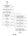
- FIG. 4illustrates a host read operation at a high level.
- FIG. 5illustrates a host write operation at a high level.
- FIG. 6illustrates an organization of flash memory.
- FIG. 7illustrates a relationship between a flash memory group and a flash port.
- FIG. 8illustrates input and output signals to a flash memory device.
- FIG. 9illustrates input and output signals to a flash HEMi block.
- FIG. 10illustrates connections between a flash port and a flash memory bank.
- FIG. 11illustrates multiplexing of CS and RB signals onto a single pin.
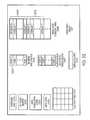
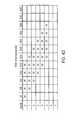
- FIG. 12illustrates a flash memory hierarchy
- FIG. 13illustrates the organization of an SPage sector.
- FIG. 14illustrates the organization of a flash page.
- FIG. 15illustrates an organization of data within a SuperBlock.
- FIG. 16illustrates a stripe organization of data.
- FIG. 17illustrates data and control flow through host ports.
- FIG. 18illustrates a host port
- FIG. 19illustrates primitive match logic
- FIG. 20illustrates a command parser block.
- FIG. 21illustrates a command distribution block
- FIG. 22illustrates connections between HEMi's and shared RAM data structures through a crossbar switch.
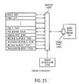
- FIG. 23illustrates a RAM controller
- FIG. 24illustrates the relationship between a shared RAM controller and a shared RAM bank.
- FIG. 25illustrates DRAM channels.
- FIG. 26illustrates HEMi stages.
- FIG. 27illustrates a flash HEMi and its tightly coupled logic block.
- FIG. 28illustrates receive HEMi and transmit HEMi unique registers.
- FIG. 29illustrates the contents of a flash HEMi mRAM.
- FIG. 30illustrates the transfer of a data block from shared RAM.
- FIG. 31illustrates ECC logic
- FIG. 32illustrates the contents of a data path DRAM.
- FIG. 33illustrates a forward table
- FIG. 34illustrates a reverse table
- FIG. 35illustrates a SuperBlock metadata table
- FIG. 36illustrates an IOP data buffer.
- FIG. 37illustrates a CDBinfo.
- FIG. 38illustrates an IOP
- FIG. 39illustrates a transfer request
- FIG. 40illustrates a page request
- FIG. 41illustrates the contents of a shared RAM block.
- FIG. 42illustrates initiator information
- FIG. 43illustrates SLC flash write timing.
- FIG. 44illustrates MLC flash write timing
- FIG. 45illustrates steps followed by a host port when a host command is received.
- FIG. 46illustrates the initial phases of handling of a CDB.
- FIG. 47illustrates special-case CDB handling.
- FIG. 48illustrates the manner in which IOPs and transfer requests are set up based on a CDBinfo.
- FIG. 49illustrates the manner in which a flash HEMi sets up page requests
- FIG. 50illustrates the flash HEMi execute loop.
- FIG. 51illustrates the page request read handler.
- FIG. 52illustrates a flash read operation in greater detail.
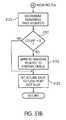
- FIG. 53illustrates the execution of a page request write handler.
- FIG. 54illustrates allocation of a SuperPage to a page request.
- FIG. 55illustrates clean-up of a completed transaction.
- FIG. 56illustrates a garbage collection process
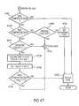
- FIG. 57illustrates a patrol function process
- FIG. 58illustrates a rebuilding process
- the system described hereinis designed to operate with various enterprise-level mass storage protocols, including SAS (“Serial Attached SCSI”), FC (“Fibre Channel”) and FC-AL (“Fibre Channel Arbitrated Loop), all of which are based on the Small Computer Systems Interface (“SCSI”), and Serial ATA (“SATA”) protocols.
- SASSerial Attached SCSI
- FCFibre Channel
- FC-ALFibre Channel Arbitrated Loop
- SATASerial ATA
- SCSI ProtocolAs a matter of convenience, the protocols relevant herein are oftentimes referred to collectively as the “SCSI Protocol,” though, as should be understood, this includes non-SCSI protocols and does not include those SCSI protocols that are not relevant.
- the system described hereinincludes a novel architecture for controlling a mass storage module consisting of flash memory chips.
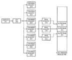
- the overall systemis illustrated in a high level overview in FIG. 1 .
- the elements shown in FIG. 1are conceptual in nature, showing the nature of interrelationships among functional blocks, and are not intended to represent actual, physical circuit-level implementations.
- Hosts 101 and 102are conventional host devices, e.g., two servers that use mass storage resources or two host bus adapters serving one such server. In certain protocols, each Host may support multiple initiators. In SCSI-based systems, initiators are host-side endpoints for data transfers, and may constitute separate physical devices or processes.
- Board 103represents one or more PCBs. It could, for example, consist of a single PCB board, or of multiple boards connected together in a mother-daughter configuration.
- Board 103is designed so that, from the perspective of Hosts 101 and 102 , Board 103 appears to constitute a conventional, rotating disk mass storage device. This requires that Host Ports 104 and 105 be designed so that they are physically and logically indistinguishable from conventional mass storage interfaces for which Hosts 101 and 102 have been designed. Thus, in the currently preferred embodiment, use of Board 103 does not require any redesign of Hosts 101 or 102 .
- SSD Controller 106represents a single integrated circuit device that is attached to Board 103 and runs at 200 MHz. In alternate embodiments, SSD Controller 106 can consist of more than one integrated circuit device, without departing from the principles of the invention(s) described herein. Clock speed, of course, represents an implementation choice, and will vary among implementations.
- Data Path DRAM 107is a 64-bit wide 256 Mbyte DDR SDRAM with a clock speed of 200 MHz sold by Micron Technology, Inc. of Boise, Id., under the product designation MT47H16M16BC-5E.
- Thisprovides an effective rate of 128 bits of data transfer per cycle, consisting of two 64-bit transfers per cycle. For purposes of simplicity, this will be described herein as a 128-bit interface.
- This deviceautomatically checks ECC on all transfers.
- the Micron MT47H32M16CC-5Ea 512 Mbyte DDR SDRAM, can be substituted.
- Data Path DRAM 107communicates with SSD Controller 106 , but does not have any direct connection to any other element in the system.
- Flash Memory Module 108represents a number of flash memory chips.
- Flash Memory Module 108consists of 192 2 gigabyte NAND flash chips, each running at 40 MHz. As is explained below, this configuration provides 300 gigabytes of user data capacity.
- the described systemcan operate with a larger or smaller overall capacity, with flash memory chips that have more or less capacity than 2 gigabytes and with flash memory chips that operate faster or slower than is currently preferred.
- Flash Memory Module 108may consist of multiple “daughter boards” that are stacked together.
- Flash Memory Module 108communicates with SSD Controller 106 , but does not have any connection with any other element in the system.
- SSD Controller 106occupies a central location, since it communicates with all other elements in the system, none of which communicate with each other.
- the design and operation of each of the elements shown as part of Board 103will be described in detail below.
- SSD Controller 106operates by accepting commands from a host and breaking those commands into smaller tasks that eventually result in a sequence of reads and writes in Flash Memory Module 108 .
- FIG. 2illustrates this process at a high level.
- SSD Controller 106When SSD Controller 106 receives a Host-initiated read or write command, it creates a data structure known as a “CDBinfo” (e.g., CDBinfo 201 ), which contains the Command Descriptor Block (“CDB”) or other corresponding command-related information from the Host. Among other information, the CDBinfo specifies the address range to be read from or written to, in Logical Block Addresses (“LBAs”).
- LBAsLogical Block Addresses
- SSD Controller 106Based on the CDBinfo, SSD Controller 106 creates a data structure known as an “Input-Output Process” (“IOP”) (e.g., IOP 202 ). Under most circumstances, a single IOP controls the entire transaction requested by the Host.
- IOPInput-Output Process
- Each IOPcan invoke up to seven data structures known as “Transfer Requests” (e.g., Transfer Requests 203 - 209 ). Each Transfer Request is designed to handle a portion of the LBA range specified by the IOP.
- Each Transfer Requestcan invoke up to three data structures known as “Page Requests” (e.g., Page Requests 210 , 211 and 212 , invoked by Transfer Request 206 ; Page Requests invoked by the other Transfer Requests are not shown in FIG. 2 ).
- Page Requestsare designed to read from or write to a segment of Flash Memory Module 108 corresponding to a portion of the LBA range specified by the Transfer Request.
- each SuperPagee.g., SuperPages 213 , 214 and 215 .
- each SuperPageconsists of four flash Pages, each of which is stored on a different Flash Die.
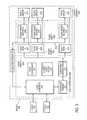
- FIG. 3provides additional detail to the overall system design illustrated in FIG. 1 , though, as before, numerous elements and details are omitted for purposes of clarity.
- FIG. 3shows Hosts 101 and 102 connected to Board 103 , with Board 103 including SSD Controller 106 , Data Path DRAM 107 and Flash Memory Module 108 .
- Flash Memory Module 108is divided into eight Flash Groups, designated as Flash Groups 0 - 7 . Of these, three are shown in the Figure: Flash Groups 0 , 1 and 7 , designated as 301 , 302 and 303 . In the currently preferred embodiment, Flash Memory Module 108 can hold between eight and twelve Flash Groups.
- SSD Controller 106also contains a number of Flash Ports equal to the number of Flash Groups contained in Memory Module 108 , e.g., Flash Ports 304 , 305 and 306 . Each Flash Port communicates with one Flash Group (e.g., Flash Port 0 304 communicates with Flash Group 0 301 ). As with the Flash Groups, in the currently preferred embodiment, SSD Controller 106 can have a minimum of eight and a maximum of twelve Flash Ports and the embodiment illustrated contains eight, of which three are shown. As is described below, each Flash Port operates independently, thereby supporting parallel operations in the Flash Groups.
- Each Flash Portincludes a Flash HEMi and a Stage Buffer (e.g., Flash Port 0 304 contains Flash HEMi 0 307 and Flash Stage Buffer 0 308 ).
- “HEMi”stands for Hardware Execution MachIne. HEMi's are logic blocks that operate as dedicated, special-purpose microprocessors. The design and function of HEMi's is explained in greater detail below.
- Each Flash HEMicontrols transfer operations for a single Flash Group (e.g., Flash HEMi 0 307 controls Flash Group 0 301 , Flash HEMi 1 309 controls Flash Group 1 302 , etc.)
- Flash Stage Buffers(e.g., Flash Stage Buffer 0 308 ) are used to buffer data transfers between Data Path DRAM 107 and the Flash Groups.
- each Flash Stage Bufferis a dual port SRAM that can handle one read and one write concurrently, and is capable of holding 16 Kbytes of data, representing four flash pages. As is explained below, this constitutes a “SuperPage” of data.
- the data interface from each Flash Groupis capable of transmitting 32 bits at a time (one doubleword), whereas Data Path DRAM 107 is capable of sending or receiving data 128 bits at a time (as is described above, in the current embodiment, the Data Path DRAM transmits and receives data in 64-bit chunks, but does so twice in each clock, thereby providing an effective data rate of 128 bits).
- the Flash Stage Buffersbuffer communications between the Flash Groups and the Data Path DRAM and therefore allow transfers to occur without requiring wait states on the part of the DRAM.
- the Flash Stage Buffersaccept the data in doubleword chunks. Once a sufficient amount of data has been received (preferably an entire SuperPage), the Flash Stage Buffer then burst transfers the data to the Data Path DRAM in a DMA transfer that uses the entirety of the Data Path DRAM data bus.
- the Flash Stage Buffersare controlled by DMA logic that handles DMA transmissions to and from the DRAM (see discussion of FIG. 10 , below).
- Hosts 101 and 102communicate with Host Interface 310 , which, as should be understood, includes Host Ports 104 and 105 (not shown).
- Hostsissue commands, provide data that is to be written into mass storage and request data from mass storage.
- the details of the manner in which Hosts communicate with mass storageis protocol-dependent.
- Hostscommunicate with mass storage using “frames,” which contain commands and/or data.
- commandsare contained in Command Descriptor Blocks (“CDBs”), which are familiar to those of ordinary skill in the art.
- CDBsCommand Descriptor Blocks
- Host Interface 310is designed to respond to CDBs in a manner transparent to the Host, meaning that from the perspective of Host 101 , Host Interface 310 appears to constitute an interface to a conventional mass storage device.
- Control flowproceeds as follows (each of the logic blocks and metadata structures mentioned is explained in greater detail below):
- Host Interface 310Upon receiving a CDB requesting a read or write, Host Interface 310 generates a CDBinfo to handle the operation (e.g., CDBinfo 201 ). That CDBinfo is then passed to Command Parser Block 311 .
- Command Parser Block 311Upon receiving a CDBinfo, Command Parser Block 311 performs coherency and other types of checks, which are described below, and then passes the CDBinfo to Command Distribution Block 312 .
- Command Distribution Block 312evaluates the CDBinfo and creates an IOP (e.g., IOP 202 ) to carry out the requested transfer. Command Distribution Block 312 then generates one or more Transfer Requests (e.g., Transfer Requests 203 - 209 ), each to carry out a portion of the transfer required by the IOP. For each Transfer Request, Command Distribution Block 312 then determines which Flash Group contains the data to be read, or the address location to be written.
- IOPe.g., IOP 202
- Command Distribution Block 312then passes the Transfer Requests to the Flash Ports corresponding to the Flash Group containing the relevant flash memory addresses, e.g., Flash Port 0 304 , Flash Port 1 305 and Flash Port 7 306 .
- the Flash HEMi for that Flash Portbreaks the Transfer Request into Page Requests (e.g., Page Requests 210 , 211 and 212 ) and uses the Page Requests to control actual read and write operations in the associated Flash Group, with each Page Request accessing up to a SuperPage of data.
- Page Requestse.g., Page Requests 210 , 211 and 212
- Control flow in FIG. 3 for a read or write operation in Flash Group 0thus proceeds as follows.
- Host 101⁇ Host Interface 310 ⁇ Command Parser Block 311 ⁇ Command Distribution Block 312 ⁇ Flash HEMi 0 307 ⁇ Flash Group 0 301 .
- Flash Stage Buffer 0 308is connected to Flash Group 0 301
- Flash Stage Buffer 1 314is connected to Flash Group 1 302
- Flash Stage Buffer 7 315is connected to Flash Group 7 303 .
- FIG. 3also shows RAM Controller 317 and Shared RAM Block 318 , each of which is described in greater detail below.
- Shared RAM Block 318contains memory used by the HEMi's
- RAM Controller 317contains logic that controls Data Path DRAM 107 and Shared RAM Block 318 and arbitrates access to both of those resources.
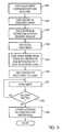
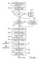
- FIG. 4illustrates the high-level data flow for a read operation handled by SSD Controller 106 .
- Step 401the Host (e.g., Host 101 ) issues a read command, including the LBA of the data.
- SSD Controller 106identifies the location of the requested LBA(s) in Flash Memory Module 108 and issues one or more read commands to the Flash Memory Module.
- Step 403Flash Memory Module 108 performs a read operation and returns data to SSD Controller 106 .
- Step 404the returned data is passed through SSD Controller 106 and stored in Data Path DRAM 107 .
- Step 405a check is made to determine if all of the data requested by Host 101 has been obtained. If not, (“no” outcome to Step 405 ), control returns to Step 403 so that the additional data can be obtained from the Flash Memory Module and stored in the Data Path DRAM.
- Step 406the data is read out of Data Path DRAM 107 and into SSD Controller 106 .
- Step 407the data is transmitted from SSD Controller 106 to Host 101 , and the read operation requested by Host 101 is complete.
- FIG. 4describes the read operation using high-level conceptual steps, the details of which are explained below.
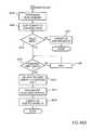
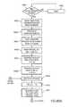
- FIG. 5uses similar high-level conceptual steps to illustrate a write operation, in which Host 101 is seeking to store data in memory.
- Step 501Host 101 issues a write command, with an LBA, and provides the data to SSD Controller 106 .
- SSD Controller 106stores the data to be written in Data Path DRAM 107 .
- SSD Controller 106identifies the location of the LBA in Flash Memory Module 108 .
- Step 504SSD Controller 106 issues a read command to Flash Memory Module 108 sufficient to read the SuperPage containing the LBA. This read command does not store data into the DRAM, and therefore proceeds from Step 403 of FIG. 4 to Step 405 , skipping Step 404 , and loops through those two Steps until all of the data has been received.
- Step 505the data from Data Path DRAM 107 is transferred to the Controller and integrated with the data read from the Flash Memory Module.
- the Controllernow holds a SuperPage in which the new data has overwritten the old data stored at that LBA, but all other LBAs in the SuperPage are unchanged.
- Step 506SSD Controller 106 issues a write command to Flash Memory Module 108 .
- Step 507Flash Memory Module 108 performs a write operation.
- Step 508a check is done to determine if all information has been written in Flash Memory Module 108 .
- Step 508If additional write operations are required (“no” result from Step 508 ), control returns to Step 507 .
- Step 509SSD Controller 106 updates location information for the LBAs that were written. As is explained in detail below, because of the nature of flash memory, a write operation does not physically overwrite the existing SuperPage, but instead writes the updated SuperPage to a new location in Flash Memory Module 108 , thereby requiring an update to the address translation information associated with the LBAs stored in that SuperPage.
- FIG. 6illustrates the organization of one Flash Group (e.g., Flash Group 0 301 ), and its relationship to its associated Flash Port (e.g., Flash Port 0 304 ). As should be understood, the details of this organization may differ in different embodiments.
- Flash Group 301consists of eight Flash Chips, designated as 601 - 608 . Each Flash Chip includes two Dies; e.g., Flash Chip 601 contains Dies 609 and 610 .
- each Die(e.g., Die 609 ) has a raw capacity of approximately 1.11 gigabytes, consisting of 8224 blocks, each made up of 64 pages, with each page consisting of 2212 bytes.
- system and spare memory spaceis subtracted, this leaves a user data capacity of approximately 1 gigabyte per die, or 2 gigabytes per NAND flash chip.
- thisprovides a raw user memory space of approximately 384 gigabytes, but the total useable space for user data is approximately 300 gigabytes, since some space is devoted to spare and system functions that do not fall within the LBA address space made available to users.
- System spacestores various types of system metadata, including SCSI mode pages, and also contains free space.
- each four-Die chiphas two CE and RB Pins, with two Dies sharing each Pin, then from the perspective of SSD Controller 106 , the two Dies that share common CS and RB Pins will appear indistinguishable from a single Die described above (e.g., Die 609 ).
- the currently preferred embodimentalso operates equally well with 1 Gigabyte NAND flash chips, each containing 2 half-gigabyte dies. In this configuration, only 4112 blocks are included per die. Other than the capacity, this configuration operates the same as the configuration described above.
- flash memory chipsthemselves are of conventional design, and the illustration in FIG. 6 is not intended to convey details of the internal design of these chips, but instead to allow for an understanding of the organization of the chips and the manner in which the Dies interface with the rest of the system.
- Flash Group 301is divided into four Banks ( 611 , 612 , 613 and 614 ), each made up of four Dies.
- Bank 611consists of Die 609 from Flash Memory 601 , Die 615 from Flash Memory 602 , Die 616 from Flash Memory 603 and Die 617 from Flash Memory 604 .
- Bank 612consists of Die 610 from Flash Memory 601 , Die 618 from Flash Memory 602 , Die 619 from Flash Memory 603 and Die 620 from Flash Memory 604 .
- Banks 613 and 614are similarly organized among the other Flash Memories and Dies.
- FIG. 6shows four Banks.
- each Flash Groupcontains between four and eight Banks, depending on the amount of capacity desired by the user.
- FIG. 7provides additional details regarding the interconnections between Flash Memory Module 108 , SSD Controller 106 and Data Path DRAM 107 .
- FIG. 7shows Flash Group 0 301 and Flash Port 0 304 , the same interconnections exist between all Flash Groups and their accompanying Flash Ports and Data Path DRAM 107 .
- Flash Group 0 301is connected to Flash Port 0 304 by two buses, Flash Bus 701 and CS/RB Bus 702 .
- CS/RB Bus 702consists of a separate line connecting Flash HEMi 307 to each of the Banks of Flash Group 301 .
- CS/RB Bus 702consists of four lines: Line 703 , connecting Flash HEMi 307 with Bank 614 , Line 704 , connecting Flash HEMi 307 with Bank 613 , Line 705 , connecting Flash HEMi 307 with Bank 612 , and Line 706 , connecting Flash HEMi 307 with Bank 611 .
- CS/RB Bus 702would consist of a correspondingly larger number of signals.
- the signals from Flash HEMi 307travel through pins on SSD Controller 106 .
- FIG. 7is not intended to show the physical details of the transmission paths, but instead illustrates the flow of data and control signals.
- CS/RB Bus 702carry Ready-Busy (“RB”) signals from Flash Group 301 to Flash HEMi 307 , and Chip Select (“CS”) signals from Flash HEMi 307 to Flash Group 301 .
- RBReady-Busy
- CSChip Select
- Flash Bus 701Address and control information from Flash HEMi 307 is transmitted on Flash Bus 701 to each of the Banks. This includes Control Signals 708 (described below in connection with FIG. 8 ) and Address/Command Signals 709 (described below in connection with FIG. 9 ).
- Bus 707connects Flash Stage Buffer 308 to Flash Bus 701 . Data is transmitted from Stage Buffer 308 , on Bus 707 , along Flash Bus 701 and to the Banks. Data is transmitted from the Banks to Stage Buffer 308 in the opposite direction.
- Data Path DRAM 107is connected to Stage Buffer 308 .
- datapasses from Data Path DRAM 107 to Stage Buffer 308 , and is then sent along Bus 701 to the Bank that has the currently active CS signal.
- Data from Flash Group 301is transmitted to Data Path DRAM 107 along the opposite path.
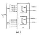
- FIG. 8shows portions of the pin-out of a single flash memory chip, e.g., Flash Chip 601 , which includes Dies 609 and 610 .
- the Flash Chipsuse a standard NAND flash interface, typically consisting in relevant part of 8 bits of address/data ( 801 ), 4 bits of control (Address Latch Enable (“ALE”) Signal 802 , Command Latch Enable (“CLE”) Signal 803 , Write Enable (“WE”) Signal 804 and Read Enable (“RE”) Signal 805 , which collectively are referred to as Control Signals 708 ), one Chip Enable pin per Die (this is connected to the CS signal from the Controller and the designations Chip Enable and Chip Select will sometimes be used interchangeably), and one Ready/Busy line per die.
- the A/D signals 801 and the ALE, CLE, WE and RE signalsare all connected to Flash Bus 701 , though these are not the only signals connected to that Bus.
- ALE, CLE, WE, RE and both Chip Enable signalsare inputs to Flash Memory 601 .
- A/D Bus 801is made up of eight bidirectional signals. Both RB signals are outputs.
- each Diehas an associated Flash Page Buffer that can hold one page of data that is being written into or read out of the corresponding Die.
- FIG. 8shows these as Page Buffers 806 and 807 .
- FIG. 9illustrates the portion of the signal output of a Flash HEMi (e.g., Flash HEMi 307 ) which is devoted to a Flash Memory Port (e.g., Flash Memory Port 0 304 ).
- Flash HEMi 307also has additional inputs and outputs devoted to other functions.
- signals connecting Flash HEMi 307 with the Flash Groupare routed through pins of SSD Controller 106 . Neither those pins, nor the logic that handles the routing, are shown.
- FIG. 9is intended as a conceptual illustration, and is not intended to illustrate the details of actual physical layout.
- Flash HEMi 307This portion of Flash HEMi 307 's interface is made up of signals devoted to the following functions:
- Control Signals 708made up of four control lines: ALE Signal 802 , CLE Signal 803 , WE Signal 804 and RE Signal 805 . These signals are outputs from Flash HEMi 307 .
- CS/RB Bus 702which is made up of CS/RB Lines 703 - 706 .
- each Flash HEMican control one Flash Memory Bank per connected CS/RB Line.
- Flash HEMi 307controls four Flash Memory Banks (e.g., Banks 611 , 612 , 613 , 614 shown in FIG. 6 ).
- each Flash HEMiwould have eight signals devoted to this purpose (note that the logic necessary to support the extra four signals is present even if those signals are not in fact used).
- CS/RB Bus 702transmits CS signals from HEMi 307 to the Flash Banks, and transmits RB signals from the Flash Blanks to HEMi 307 . Since the signals are multiplexed in this manner, each such Line may transmit only one type of signal at a time.
- the CS/RB signalsare “one hot” signals, meaning that one and only one of these signals can be active at any given time.
- SSD Controller 106uses the same signals for both CS and RB purposes to save pins on SSD Controller 106 , and therefore reduces the cost and complexity of the SSD Controller. However, this limits the number of Banks that can be controlled by Flash HEMi 307 , since one RB signal, and therefore one pin, is required for each bank. Because in the current embodiment SSD Controller 106 includes eight CS/RB pins for each Flash Port, in that embodiment a maximum of eight Banks may be controlled by each Flash HEMi.
- Address/Command Signals 709This bus, which connects to Flash Bus 701 , runs at the same 40 MHz speed as the flash memory chips and carries addresses and commands from Flash HEMi 0 307 to Flash Group 0 301 .
- Address/Command Signals 709can be thought of as four separate eight-bit buses (consisting of lines 0 - 7 , 8 - 15 , 16 - 23 and 24 - 31 ), each of which routes an eight-bit payload to a separate Die in a Flash Memory Bank. Thus, eight lines from Address/Command Bus 709 connect to A/D signals 801 , shown in FIG. 8 .
- each Flash Port44 pins of SSD Controller 106 are devoted to each Flash Port (keeping in mind that each Flash Port can support a maximum of eight Banks and therefore requires eight CS/RB pins, though only four such signals are shown in FIG. 9 ). Since SSD Controller 106 can support up to 12 Flash Ports, 528 pins of SSD Controller 106 are devoted to the flash interface, though some of these pins may be no-connects, if fewer than 12 Flash Ports are used. Note that, if separate CS and RB pins were required, an additional 96 pins would be needed for the flash interface (1 pin per Bank ⁇ 8 Banks ⁇ 12 Flash Ports). Combining the CS and RB signals onto a single pin therefore provides a very significant savings in terms of the number of required pins.
- the embodiment shown in FIG. 9is currently preferred, but various other embodiments are also possible.
- the eight CS/RB pins currently devoted to a particular Flash Groupare connected to a mux or other similar logic device located in the Flash Group.
- the muxhas a set of output signals that connect to the CE inputs of all Flash Dies in a Bank, with each signal causing the CE inputs of a particular Bank to be selected. Because the eight SSD Controller CS/RB pins are capable of transmitting 256 separate states, in theory, it would be possible to use those pins to select among 256 separate Banks, by designing the mux or other logic so as to generate a signal along a different output line for each of the 256 possible input states.
- each Flash HEMicould check the RB state of the Banks using the A/D Bus.
- This alternate embodimenttherefore allows SSD Controller 106 to devote fewer pins to the flash memory interface or to support a larger number of Banks with the same number of pins, though at the cost of some additional logic complexity.
- FIG. 10illustrates the manner in which the Dies in a single Bank (e.g., Dies 609 , 615 , 616 and 617 in Bank 611 ) are connected together and to the associated Flash Port (e.g., Flash Port 0 304 , containing Flash HEMi 307 and Stage Buffer 308 ).
- the Dies in a single Banke.g., Dies 609 , 615 , 616 and 617 in Bank 611
- the associated Flash Porte.g., Flash Port 0 304 , containing Flash HEMi 307 and Stage Buffer 308 .
- Die 609is one of two Dies in Flash Chip 601
- Die 615is one of two Dies in Flash Chip 602
- Die 616is one of two Dies in Flash Chip 603
- Die 617is one of two Dies in Flash Chip 604 .
- FIG. 10only shows one of the two Dies in each Flash Chip. (As is described above, Memory Module 108 may well incorporate Flash Chips that have four Dies each (or more), though the principles of the design disclosed herein would remain the same).
- Line 706constitutes the CS/RB signal interface between Flash HEMi 307 and Bank 611 . That Line carries the CS signal from Flash HEMi 307 to Bank 611 , and the RB signal from Bank 611 to Flash HEMi 307 .
- FIG. 10illustrates this by showing arrows going in both directions between Flash HEMi 307 to Point 1001 on Line 706 . From Point 1001 , the signal path divides, and carries the CS signal as an input to the Dies (shown by arrows pointing into each Die with the label “CS”) and carries the RB signal as an output from each of the Dies (shown by arrows pointing out of each Die with the label “RB”).
- Point 1001is figurative in nature, and neither it nor the rest of the Figure are intended as a literal illustration of physical implementation.
- the RB output signals from each Die in the Bankare logically ORed together (or otherwise similarly combined), so that a Busy signal is sent from Bank 611 to HEMi 307 along Line 706 if any one of the four Dies in the Bank is outputting “Busy.”.
- Line 706also carries the CS signal from Flash HEMi 307 to each of the Dies in the Bank.
- the CS signal devoted to the Bankis set by Flash HEMi 307 , that signal is sent simultaneously to the CE pin of each Die in the Bank, thereby selecting each such Die simultaneously.
- FIG. 10also shows Address/Command Bus 709 , which represents the connections between the A/D pins of Flash Chips 601 - 604 and the Address/Command signals of HEMi 307 .
- 32-bit Bus 709carries signals from Flash HEMi 307 to Bus Switch 1002 .
- Bus Switch 1002represents logic that combines, divides and routes signals as described, and does not necessarily constitute a single physical switch.
- Bus Switch 1002divides the signals from Bus 709 into sub-buses. Signals 0 - 7 are transmitted to the A/D pins of Flash Chip 601 using 8-bit Bus 801 (also shown in FIG. 8 ), Signals 8 - 15 are transmitted to the A/D pins of Flash Chip 602 using 8-bit Bus 1003 , Signals 16 - 23 are transmitted to the A/D pins of Flash Chip 603 using 8-bit Bus 1004 and Signals 24 - 31 are transmitted to the A/D pins of Flash Chip 604 using 8-bit Bus 1005 . Note that the A/D pins are shared by both Dies in a Flash Chip, so that the signals transmitted to the Flash Chip pins would be received by the appropriate Die in a manner specific to the internal design of the Flash Chips.
- FIG. 10also shows the connections between Control Signals 708 of Flash HEMi 307 and each of the Dies. As is described above, these Control Signals consist of ALE, CLE, RE and WE, and they are transmitted from Flash HEMi 307 to the Flash Dies. Control Signals 708 are sent from Flash HEMi 307 to Bus Switch 1002 . From Bus Switch 1002 , an identical set of Control Signals (designated in each case as 708 ) is transmitted to each of the Flash Memory Chips. As with the A/D pins, the ALE, CLE, RE and WE pins are shared by both Dies in each Flash Memory Chip.
- FIG. 10also shows Flash Stage Buffer 308 , which is connected to Bus Switch 1002 by 32-bit Bus 707 . Unlike Bus 709 , Bus 707 is bidirectional, and thus transmits data in both directions.
- Stage Buffer DMA Controller 1006Transfers between Stage Buffer 308 and the Dies occur under the control of Stage Buffer DMA Controller 1006 .
- Flash Stage Buffer 308also connects to the RE and WE inputs of Flash Chips. These connections, which for clarity's sake are not shown in the Figures, are used to control DMA operations.
- Bus Switch 1002divides the signals from Bus 707 into four sets of eight-bit signals, and transmits those signals to Dies 609 , 615 , 616 and 617 using 8-bit Buses 801 , 1003 , 1004 and 1005 . Similarly, Bus. Switch 1002 receives data from Dies 609 , 615 , 616 and 617 on 8-bit Buses 801 , 1003 , 1004 and 1005 , then transmits the entire 32-bit value to Stage Buffer 308 on Bus 707 .
- Switch 1002thus multiplexes signals from Flash HEMi 307 and signals to and from Stage Buffer 308 on the same 8-bit Buses.
- Switch 1002determines which set of signals to pass through to the 8-bit Buses depending on the particular stage of the read or write cycle, with address information from Flash HEMi 307 being connected to the Dies during one stage of the cycle, whereas data to or from Stage Buffer 308 is connected to the 8-bit Buses during a different stage of the cycle.
- Switch 1002is conceptual in nature and does not necessarily constitute a single dedicated switch. In addition, aspects of the functionality described in connection with Switch 1002 may be found in other logic blocks).
- FIG. 10shows only a single Flash Memory Bank, 611 .
- Bus Switch 1002would interface to each of the Flash Memory Banks in the Flash Group, and each interface would duplicate all of the signals output from Bus Switch 1002 to Bank 611 that are shown in FIG. 10 , with the exception of Signal 706 , which, as is explained above, is specific to Bank 611 .
- Flash Memory Switch 1002connects Buses 707 , 708 and 709 to each of the Flash Banks, but the only Bank that is responsive is the Bank associated with the currently active CS signal from Flash HEMi 307 .
- Flash Bus 701includes Buses 708 , 801 , 1003 , 1004 and 1005 .
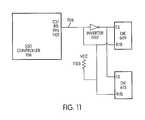
- FIG. 11shows the CS and RB logic related to Line 706 in greater detail.
- SSD Controller CS/RB Pin 1101connects to the RB and CE pins associated with Flash Dies 609 and 615 .
- Dies 609 and 615are two of the four Dies in Bank 611 .
- the other two dies in the Bankare not shown, but are connected in the same manner as Dies 609 and 615 .
- SSD Controller 106drives CS/RB Pin 1101 high to select Bank 611 . This signal is inverted by Inverter 1102 and received low by the CE pins of the Dies in the Bank. These pins are active low.
- CS/RB Pin 1101is driven low by SSD Controller 106 when the Controller is driving another one of the CS pins in the same Flash Group high (thereby selecting another Bank in the Flash Group).
- SSD Controller 106floats CS/RB Pin 1101 .
- the CS/RB PinWhen the CS/RB Pin is floated by the SSD Controller, that Pin will receive a low input if any of the Flash Die RB pins is driving a low signal, indicating that the Bank is busy, since a low output on any of the Die RB pins will override Pullup 1103 . If, on the other hand, the Bank is in the Ready state, the Flash Dies allow the RB pins to float. Because Pullup 1103 is connected to the RB pins, when all of those pins are floated, and when CS/RB Pin 1101 is floated, the Pin receives a high input signal, which indicates that the Bank is ready.
- this circuitconnects the R/B pins of the Banks together in an OR configuration, since all of the pins must be in the Ready state (floating) in order for a ready signal to be received by CS/RB Pin 1101 , so that the circuit effectively ORs together the Busy state of the Pins.
- Inverter 1102allows SSD Controller 106 to drive the CS signal high to select a Bank, even though the Bank's CE pins are active low. This is necessary because the CS signal must be driven high in order to override the incoming RB signal.
- the RB input to SSD Controller 106can be active high, but can still be overridden by a high output on CS/RB Pin 1101 , since a high CS output will override a high RB input created by Pullup 1103 .
- Hostssuch as 101 and 102 typically organize memory in terms of Logical Block Addresses, or “LBAs.”
- LBAsLogical Block Addresses
- the HostWhen a Host writes data to mass storage, the Host typically transmits a CDB that contains a write command and an LBA, though the details of Host communication vary depending on the specific protocol used by the Host.
- the HostWhen the Host subsequently wishes to read that data, it issues a read command using the same LBA.
- a Host's memory architecturedivides data into millions of LBAs, with each LBA numbered sequentially, beginning with LBA 0 .
- a Hostwill often communicate with a number of mass storage controllers, and will assign a subset of the Host's overall LBA range to each controller.
- SSD Controller 106responds to an LBA range that begins with LBA 0 and ends with the highest LBA addressable by the Controller. Mapping that sequence of LBAs onto a larger Host LBA address space is the responsibility of the Host or a host bus adapter, and is transparent to SSD Controller 106 .
- FIG. 12illustrates the memory hierarchy used in Flash Memory Module 108 in the currently preferred embodiment.
- Each Flash Groupis made up of a number of Banks (e.g., Bank 611 ). Each Bank consists of a number of Blocks, designated as Block 0 -Block n (e.g., Block 0 1201 ). As is commonplace in flash memory systems, a Block represents a segment of flash memory that is erasable in a single operation.
- the exact number of Blocks stored in a Bankis implementation-dependent. To take one example, in a system providing 300 gigabytes of available user data, the number of Blocks per Bank would ordinarily be in the range of 7,000-9,000, depending on various factors, including defect management and the amount of memory set aside for free space.
- each Blockconsists of 64 SuperPages, designated as SuperPages 0 - 63 .
- each SuperPageconsists of four flash Pages (e.g., SuperPage 30 consists of Page 30 1202 , Page 30 1203 , Page 30 1204 and Page 30 1205 ). Pages 1202 , 1203 , 1204 and 1205 are stored at the same address location on four different Flash Memory Dies in the same Flash Bank. Thus, SuperPage 30 is spread across four separate Dies.
- each Pagerepresents the smallest increment of the flash memory that can be read from or written to.
- each Pagestores fifteen memory segments known as PSectors, designated as PSectors 0 - 14 .
- FIG. 12also shows an additional memory structure: SPage Sector 0 1206 .
- SPage Sector 0consists of four PSector 0 s, one on each Page.
- SPage Sector 0corresponds generally to a classic mass storage sector, but is physically spread across four PSectors, each of which is stored at the same address of a different Die on the same Bank.
- the currently preferred embodimentalso makes use of an additional memory structure that is not shown in FIG. 12 : SuperBlocks, which are made up of the same Block on each Bank in the Flash Group (e.g., Block 0 1201 is part of SuperBlock 0 of the Flash Group).
- the data and metadata associated with a particular LBAis stored in a single SPage Sector (e.g., SPage Sector 1206 ), and is referred to herein as the Sector Contents, made up of the Sector Data and the Sector Metadata.
- FIG. 13illustrates the organization of a SuperPage Sector, e.g., SPage Sector 1206 .
- the entire SPage Sectorconsists of 556 bytes in flash memory.
- Each SPage Sectoris divided into four PSectors, each consisting of 139 bytes, each on a different Flash Die.
- Sector Data Field 1301528 bytes of SPage Sector 1206 is allocated to data, shown as Sector Data Field 1301 .
- Different Host protocolsassociate differing amounts of data with a single address, so that, depending on the protocol used, Sector Data Field 1301 may be as small as 512 bytes.
- each SPage Sectoralso includes 8 bytes of End-to-End (“E2E”) information (Field 1302 ) and 20 bytes of ECC information (Field 1303 ). These Fields collectively constitute the Sector Metadata.
- E2EEnd-to-End
- E2E informationis specified by newer versions of the SCSI Protocol. This information can be used by Initiators to track data and insure that the data returned by a mass storage device matches the data requested. ECC information is used for error correction purposes.
- E2E Field 1302is further divided into RefTag Field 1304 , AppTag Field 1305 and CRC Field 1306 .
- RefTag Field 1304consists of four bytes and contains an address that may be associated by the Initiator with the Sector Data. RefTag support is not required by the SCSI Protocol (and was not part of earlier versions of the Protocol), so an Initiator may or may not use RefTags. If an Initiator does use RefTags, the value associated with RefTag Field 1304 is taken from the CDB that triggered the original write of the Sector Contents. Typically, this value is the same as the LBA, though the Initiator may assign a different RefTag. The Initiator may choose to have the RefTag value for each subsequent sector in the same write incremented, or to assign a single RefTag value for all sectors associated with a single write. If the incrementing option is chosen, SSD Controller 106 performs that operation, based on the initial RefTag value and the number of sectors received.
- SSD Controller 106fills in RefTag Field 1304 with the LBA address. This field is used by SSD Controller 106 for internal error checking purposes whether or not the Initiator requests the use of RefTags.
- RefTag Field 1304should match the RefTag value of any CDB that causes a subsequent read or write to any LBA assigned to this SPage Sector. (If no RefTag is assigned by the Initiator, the RefTag value should match the LBA based on the CDB). If the two values do not match, this indicates some type of error, which may result from a mistake in the received RefTag, data corruption in RefTag Field 1304 , or a problem in the address translation tables used by SSD Controller 106 to select SPage Sector 1206 as the appropriate target for the read or write. Such a condition, if detected, results in the issuance of an appropriate SCSI sense code to the Host, indicating a transaction failure (or other similar communication, depending on the protocol being used).
- AppTag Field 1305consists of two bytes, and is used for Initiator-specified information relating to the particular application that created the associated Sector Data. AppTag information is supported by the SCSI Protocol, but is not required. If this information is not supplied by the Initiator, AppTag Field 1305 is filled in with a default value chosen so that it will not overlap any valid AppTag value assigned by an Initiator that does support the use of AppTags.
- the AppTag information for data received from the flash memorycan be checked against an AppTag supplied by the Initiator as part of a read command, with a mismatch indicating an error.
- CRC Field 1306consists of two bytes, and contains Cyclic Redundancy Check (“CRC”) data that is used to check the integrity of the data and metadata stored in SPage Sector 1206 .
- CRCCyclic Redundancy Check
- the CRC tagcan be checked against a value received from the Initiator, to determine whether the data and metadata are correct.
- the SCSI Protocolallows an Initiator to request checking of any or all of the three E2E values.
- ECC Field 1303contains Error Correcting Code (“ECC”) information that can be used to correct errors in the LBA Data and Sector Metadata. ECC checking used in the preferred embodiment is described below in connection with FIG. 31 .
- each Page(e.g., Page 1202 ) consists of 2212 bytes of flash memory space, and includes 15 PSectors, designated in each case as PSector 0 - 14 , plus metadata (not shown).
- each of the four PSectors that make up an SPage Sectorstores one-quarter of the Sector Contents that are stored in that SPage Sector. That data is allocated among the PSectors on a byte-interleaved basis.
- the first byte of the first doubleword of the Sector Contentsis written into the first byte of PSector 0 of Page 1202
- the second byte of the first doublewordis written into the first byte of PSector 0 of Page 1203
- the third byte of the first doublewordis written into the first byte of PSector 0 of Page 1204
- the fourth byte of the first doublewordis written into the first byte of PSector 0 of Page 1205
- the first byte of the second doublewordis written into the second byte of PSector 0 of Page 1202 , etc.
- the Sector Contents stored in SPage Sector 0are spread among the four PSectors 0 .
- each of the four Pagesstores one-quarter of the Sector Contents, or 139 bytes (556/4).
- FIG. 14illustrates Flash Page 1202 in additional detail, showing elements that are not shown in FIG. 12 .
- a flash pageconsists of 2048 bytes of data and/or metadata plus an additional 64 “spare” bytes used for other purposes, adding up to a total of 2212 bytes.
- each Pageconsists of 2212 bytes, 2085 of those bytes are used for Sector Contents (15 ⁇ 139), and the extra 27 bytes store metadata associated with the SuperPage.
- FIG. 14shows PSectors 0 - 14 , consisting of 2085 bytes, and SuperPage Metadata 1401 , which consists of 27 bytes per flash page.
- the SuperPage Metadatais spread across all four Flash Pages that make up a SuperPage, so that SuperPage Metadata Field 1401 stores one-quarter of the metadata associated with the SuperPage.
- SuperPage Metadata 1401consists of SPage Index 1402 and Time Stamp 1403 .
- SPage Index 1402stores an index into a table known as the “Forward Table,” which contains physical location information for LBAs.
- the Forward Tableis described below, in connection with FIG. 33 .
- Time Stamp 1403contains a time stamp representing the time when the SuperPage was written.
- the SPage Index and Time Stampare written redundantly into each of the four Flash Pages that make up a SuperPage. The redundancy is necessary because this metadata is not protected by the ECC mechanisms that protect other information.
- SuperPage Metadata 1401is filled in by the Flash HEMi when the SuperPage is written.
- the Flash HEMiderives the SPage Index from the Page Request that initiates the write, and derives the Time Stamp information from an internal clock.
- the SuperPage Metadatais used for reconstructing open SuperBlocks following an unanticipated power loss. Power loss reconstruction is described below in connection with FIG. 58 .
- FIG. 15illustrates the manner in which Sector Contents are organized among Blocks 0 and 1 of a Bank. As should be understood, the same organization would be followed for all remaining Blocks stored in the Bank.
- Each SPage Sectorstores the Sector Contents associated with a single LBA, and the SPage Sectors of a SuperPage store Sector Contents associated with fifteen contiguous LBAs. As is explained below, however, the fifteen contiguous LBAs associated with one SuperPage may have no relationship with the fifteen contiguous LBAs associated with the next SuperPage.
- LBA(A)indicates a particular address
- LBA (A+14)indicates an LBA address that is fourteen higher than LBA (A) (e.g., if LBA(A) were LBA(0), then LBA (A+14) would be LBA(14).
- LBA(A) and LBA(B)there is no relationship between LBA(A) and LBA(B), for example, other than that each will be evenly divisible by fifteen.
- LBA(A)might represent LBA(9,000), whereas LBA(B) might represent LBA(60).
- FIG. 16illustrates the manner in which the Host address space is mapped onto Flash Memory Module 108 during initialization.
- Hoststypically issue reads and writes using LBAs, which isolate the Host from the details of the physical memory organization.
- each Flash Groupis the same size, and each stores data corresponding to the same number of LBAs (or other Host addressing scheme).
- LBAsare distributed among the Flash Groups in sets that are multiples of 45, since, as is described below, 45 LBAs is the maximum number that can be handled by a single Transfer Request.
- the currently preferred embodimentuses a stripe size of 90 LBAs, so that LBAs 0 - 89 are assigned to Flash Group 0 , 90 - 179 to Flash Group 1 , 180 - 269 to Flash Group 2 , etc., until the last Flash Group has been reached, at which point the LBA assignments loop back to Flash Group 0 .
- a variety of other striping algorithmsis possible.
- the usercould be allowed to specify the stripe size, though it would be preferable for this to be done in multiples of the number of LBAs that can be handled by a Transfer Request.
- FIG. 16shows a simplified version of the flash memory space. This simplified version is made up of three Flash Groups, designated 0 - 2 .
- a Blockconsists of two SuperPages, designated as SP 0 and SP 1 .
- Block 0 , Bank 0 of Flash Group 0consists of the data written into the slots designated 1601 .
- each Bankcontains only a single Block.
- SuperBlock 0 of Flash Group 0consists of Block 0 from each Bank, designated in FIG. 16 as 1602 (i.e., the entire Flash Group, in the simplified example).
- SuperPage 0 of Block 0 of each SuperBlockcontains a data structure known as the SuperBlock Metadata Table. This is shown as “SMT” in SP 0 of Bank 0 of each Flash Group.
- the LBAsare assigned in “stripes” of 90 LBAs each.
- the first such stripe(LBAs 0 - 89 ) is assigned to Flash Group 0 , SuperPage 0 on Banks 1 - 6 .
- the next stripe of 90 LBAs( 90 - 179 ) is assigned to Flash Group 1 , SuperPage 0 on Banks 1 - 6 .
- the next stripe(LBAs 180 - 269 ) is assigned to Flash Group 2 , SuperPage 0 , on Banks 1 - 6 .
- This method of allocating LBAstends to maximize flash memory parallelism. Because each Flash Group operates independently, it is advantageous to stripe LBAs across Flash Groups, since this maximizes the likelihood that a single transaction will address data held on more than one Flash Group, thereby allowing multiple flash reads or writes relevant to the transaction to occur simultaneously. Because a Transfer Request can only address LBAs on a single Flash Group, it is sensible to specify stripe sizes in increments of 45 (the maximum number of LBAs that can be addressed by a Transfer Request), to minimize the number of Transfer Requests required for a transaction. In the current embodiment, a stripe is made up of two such 45-LBA increments, since this represents six SuperPages.
- a Flash Groupcan handle five simultaneous write operations, on five separate Banks.
- Using a stripe size of 90 LBAstends to maximize parallel usage of the flash interface, since a large transfer can execute five simultaneous writes on each Flash Port, and can execute on multiple Flash Ports in parallel.
- This organizationtherefore contributes to the ability of SSD Controller 106 to handle large Host-initiated reads or writes quickly, using a high degree of parallelism.
- a hypothetical transfer involving LBAs 0 - 190 as shown in FIG. 16could occur using one IOP and five Transfer Requests.
- a first Transfer Requestcould handle LBAs 0 - 44
- a second Transfer Requestcould handle LBAs 45 - 89
- a third Transfer Requestcould handle LBAs 90 - 134
- a fourth Transfer Requestcould handle LBAs 135 - 179
- a fifth Transfer Requestcould handle LBAs 180 - 190 .
- this transferinvolves three different Flash Groups, thereby allowing for a high degree of parallelism.
- Page Requests that target different Bankscan operate in parallel even on the same Flash Group
- the Page Requests issued by each Transfer Request in this examplecould also operate in parallel, since each Page Request targets a different Bank.
- the allocation of LBAs to Flash Groupsis permanent.
- the allocation to Banks within a Flash Groupmay change over time.
- the Flash HEMiattempts to use a new SuperPage from the same Bank as the old SuperPage. Occasionally, however, this is not possible and the Flash HEMi will move the LBAs to a SuperPage on another Bank.
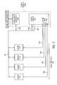
- FIG. 17shows Host Interface 310 in greater detail than is shown in FIG. 3 .
- Host Interface 310consists of Physical Interface 1701 and two separate Host Ports, designated as Host Port 0 104 and Host Port 1 105 .
- Physical Interface 1701is further described below, but for present purposes it is sufficient to understand that it routes signals between Hosts 101 and 102 and Host Ports 104 and 105 .
- Each Host Portis capable of interfacing to a separate Host.
- Host Interface 310performs the following functions on the receive side:
- Host Interface 310performs the following functions on the Transmit side:
- Each Host Portincludes a Receive HEMi ( 1702 and 1703 ), a Transmit HEMi ( 1704 , 1705 ), a Receive Stage Buffer ( 1706 , 1707 ) and a Transmit Stage Buffer ( 1708 , 1709 ).
- each Receive HEMireceives control information from one of the Hosts through Physical Interface 1701 , and communicates control information to other elements of SSD Controller 106 .
- Control informationin this context, means commands, control signals and addresses, but does not include data. Note that the control information received from the Host by each Receive HEMi may differ from the control information communicated by the Receive HEMi's.
- Each Transmit HEMireceives control information from other SSD Controller elements and communicates control information to one of the Hosts through Physical Interface 1701 . Again, the control information transmitted to a Host by a Transmit HEMi may differ from the control information received by the Transmit HEMi.
- Each Receive Stage Bufferreceives data from one of the Hosts through Physical Interface 1701 and transmits that data on to Data Path DRAM 107 .
- the Receive Stage Buffersare 16 Kbytes, which allows them to accept up to 4 FC_AL (“Fibre Channel Arbitrated Loop”) data frames.
- Each Transmit Stage Bufferreceives data from Data Path DRAM 107 and transmits that data on to one of the Hosts through Physical Interface 1701 .
- the Transmit Buffersare 4 Kbytes, which allows them to store one outgoing frame and one incoming frame from Data Path DRAM 107 .
- FIG. 18shows certain additional details regarding Host Port 0 104 .
- communications between SSD Controller 106 and Host 101are organized according to the dictates of the particular protocol used by the Host.
- the relevant protocolse.g., SAS, SATA, Fibre Channel
- frameswhich consist of defined groups of commands and data.
- SSD Controller 106Since the precise frame format used differs among the various relevant protocols, SSD Controller 106 must be modified for each protocol. SSD Controller 106 has been designed, however, so that the modifications are minimal, amounting to different firmware for the Receive and Transmit HEMi's, and a different physical connector. All other aspects of SSD Controller 106 are unchanged for the various protocols. This is a significant advantage of the pipelined and modular design of SSD Controller 106 , and also of the design of Host Interface 310 .
- a frameconsists of a Start of Frame (“SOF”) primitive, a frame header (metadata specified by the protocol, but generally including information necessary to identify the payload and possibly the Initiator), a payload (e.g., data, command, etc.), a CRC value for validation of the entire frame, and an End of Frame (“EOF”) primitive.
- SOFStart of Frame
- EEFEnd of Frame
- the receive side of Host Port 0 104is responsible for receiving the frame, dividing it into its constituent parts, and taking whatever action is needed to either route data to its intended destination and/or set up the transaction.
- the transmit side of the Host Portis responsible for receiving relevant data and command information from other elements of SSD Controller 106 and packaging that information into a frame for transmission to Host 101 .
- GigaBlaze 1801is a transceiver core available from LSI Corporation, headquartered in Milpitas, Calif., under the designation 0.11 micron GigaBlaze® GflxTM x1 Core. This core contains an 8 b/10 b encoder, a serializer/deserializer and a phy, which performs physical conversion between received bits and voltage levels.
- GigaBlaze 1801has two serial ports capable of attaching to 3 G SATA, 3 G SAS, 4 g FC_AL and 4 G FC buses. The details of the internal operation of GigaBlaze 1801 are not relevant herein, except that it handles the physical interface to the Host.
- GigaBlaze 1801is connected to Host 101 .
- FIG. 18only shows one of the two Host Ports on SSD Controller 106 , the other Host Port is identical, and contains its own GigaBlaze.
- GigaBlaze 1801is connected to Primitive Match Logic 1802 .
- the Primitive Match Logicis designed to allow the same physical level protocol to interface with various different logical level protocols that handle frames and primitives differently.
- GigaBlaze 1801receives a primitive from Host 101
- GigaBlaze 1801routes that primitive to the Primitive Match Logic, which is described in detail below in connection with FIG. 19 .
- the Primitive Match Logiccontrols Frame Router 1803 , which receives frames from GigaBlaze 1801 and routes portions of the frames under the control of the Primitive Match Logic. Data is routed to Receive Stage Buffer 0 1706 , headers are routed to Non-Data Payload FIFO 1804 and primitives are routed to Inbound Primitive FIFO 1808 .
- Receive HEMi 0 1702uses information in the Header and Primitive FIFO's to identify actions to be taken. Data routed to the Receive Stage Buffer is sent via DMA transfer to Data Path DRAM 107 .
- Receive HEMi 1702generates primitives and routes them to Outbound Primitive FIFO 1805 .
- These generated primitivesinclude ACK (acknowledging correct receipt of a frame), NAK (indicating that a frame was not received correctly) and RRDY (reporting frame credit to an Initiator).
- Primitives on Outbound Primitive FIFO 1805are inserted into transmissions to Host 101 immediately, and may be inserted in the middle of other transactions (e.g., an outbound data frame).
- Transmit Stage Buffer 0 1708contains data received from Data Path DRAM 107 that is to be transmitted to Host 101 as part of a frame responsive to a read command.
- Transmit Frame Buffers 1806consist of one or more buffers that hold metadata used to construct frames. The Transmit Frame Buffers operate similarly to the receive-side buffers, though, as should be understood, they are used to construct frames, rather than to deconstruct them.
- Cut-Through Logic 1807helps interface SSD Controller 106 to Fibre Channel networks. If SSD Controller 106 is connected to a Fibre Channel network, Primitive Match Logic 1802 evaluates received primitives to determine if the primitives are intended for SSD Controller 106 . Primitives determined not to be intended for SSD Controller 106 are sent to Cut-Through Logic 1807 . The Cut-Through Logic then passes the primitives to the GigaBlaze to be returned to the Fibre Channel network, for transmission on to the next node on the network.
- SSD Controller 106The physical connectors required for the various different protocols (SAS, SATA and Fibre Channel) are incompatible. In the currently preferred embodiment, a different version of SSD Controller 106 will exist for each protocol. However, because the Primitive Match Logic operates correctly with each of the protocols (see below), the only difference required for each protocol is the use of a different physical connector, though different firmware may also be required for the Receive and Transmit HEMi's. In a different embodiment, SSD Controller 106 could incorporate three different physical connectors, one for each protocol, and thereby allow the same physical controller to be used with any of the protocols.
- Primitive Match Logic 1802is shown in greater detail in FIG. 19 .
- This logicincludes a state machine that matches received primitives and identifies actions to be taken based on the matched primitive and on the current state.
- Primitives received from a Hostare transmitted from Gigablaze 1801 to Primitive Latch 1901 .
- the primitivesare then matched against the bit patterns contained in Primitive Match Registers 1902 , which consists of sixteen registers. If no match is found, the value from Primitive Latch 1901 is routed directly onto Inbound Primitive FIFO 1808 .
- Primitive Match Control Registers 1903consists of sixteen registers, one for each of the Primitive Match Registers.
- the Primitive Match Control Registerscontain bits that indicate which bits in the associated Primitive Match Register must match the value in Primitive Latch 1901 in order for an overall match to be found. For example, these bits may require that the first byte match, with no requirement that any other bits match.
- These bits from the Primitive Match Control Registerstherefore act as a mask, allowing multiple received primitives to match a single Primitive Match Register. This is useful in cases where the same action is to be taken for a class of received primitives, and is also useful in screening out portions of primitives that represent data rather than commands.
- Primitive Match Control Registers 1903indicate actions to be taken if the value in the corresponding register in Primitive Match Registers 1902 matches Primitive Latch Register 1901 .
- these bitscan control Frame Router 1803 so that some of the data following the primitive is moved into Non-Data Payload FIFO 1804 and data following that is moved into Receive Stage Buffer 1706 . This would generally occur in the case of an SOF primitive received in connection with a data frame.
- the Primitive Match Control Registersoperate as a state machine. For example, certain bits can set a counter (not shown) that can cause a certain number of subsequent primitives to be operated on by the current Control Register, rather than a Control Register chosen through the Primitive Match Registers. In addition, the Primitive Match Control Registers can alter the values contained in various other registers that are not shown.
- Primitive Match Logic 1802contains logic that performs comparisons between the value in Primitive Latch 1901 and Primitive Match Registers 1902 , and that implements the control functions required by Primitive Match Control Registers 1903 .
- Primitive Match Registers 1902 and Primitive Match Control Registers 1903are loaded by the associated Receive HEMi, using data overlays. These overlays are used to customize Primitive Match Logic 1802 for different protocols (e.g., SAS, SATA), since each protocol has its own set of primitives. In addition, overlays can be used to handle different sets of primitives, or different states, within a single protocol.
- the values used by the Receive HEMi to load the Primitive Match and Primitive Match Control Registersare taken from an initialization firmware code load. Thus, in many cases it will be possible to update Primitive Match Logic 1802 for new protocols or modifications to existing protocols by a modification to the Receive HEMi firmware, without any alteration to the hardware.
- Primitive Match Logic 1802also contains Frame Cracking Logic 1904 .
- This logic blockreceives the initial dword in a frame and evaluates that dword to determine the nature of the frame (e.g., data, command). Based on the type of frame, the Frame Cracking Logic routes the frame appropriately. For example, if the frame is a command frame, the Frame Cracking Logic routes the entire frame to Non-Data Payload FIFO 1804 , whereas if the frame is a data frame, the Frame Cracking Logic routes the header portion to the Non-Data Payload FIFO, and routes the data portion to the appropriate Receive Stage Buffer.
- the Primitive Match Logicis advantageous in that it allows SSD Controller 106 to handle different protocols, involving different frame encodings, without the need for software or significant hardware changes.
- the Receive Host Port designallows for more efficient transfers of data, since the data FIFO contains only data and does not contain commands or metadata, and allows data to be transferred to the Data Path DRAM via DMA transfers in parallel with Receive HEMi operations on header and primitive metadata, thereby increasing overall system performance.
- SSD Controller 106can be used for a variety of different protocols, requiring only a modification to HEMi firmware and a different physical connector. The protocols described above are all relatively similar. SSD Controller 106 can also be adapted easily for protocols with significant differences from those described above. In one embodiment, for example, SSD Controller 106 can be adapted for use with lane-oriented protocols such as PCI Express. As is understood by those of skill in the art, in PCI Express systems, external devices transmit and receive data and metadata using “lanes,” each of which carries a portion of the transmission, with doublewords of data striped across the lanes.
- the number of lanesis implementation-dependent, but SSD Controller could be adapted for use with a 4-lane PCI Express system by adding two additional GigaBlazes (as should be understood, each GigaBlaze would be a version designed for the PCI Express interface), two additional Receive HEMi's and two additional Transmit HEMi's.
- One GigaBlaze, one Receive HEMi and one Transmit HEMiwould be devoted to each lane.
- SCSI HEMi 2001(see below) is not used. That HEMi can instead be used as an additional RdWr HEMi.
- a device driver operating on the external Hostis responsible for formatting PCI Express transmissions into IOPs. Most of the Host Port logic is therefore unnecessary (e.g., Primitive Match, various FIFO's, etc.).
- the Receive and Transmit HEMi'sare responsible for destriping and restriping the data, respectively. Once a received IOP has been destriped, it can then be handed directly to a RdWr HEMi (see below). Processing then proceeds as per the other protocols described above.
- SSD Controller 106with a lane-oriented protocol such as PCI Express requires some additional modifications, these modifications are relatively minor, and easily accommodated as a result of the Controller's modular design. Addition and subtraction of HEMi's is relatively simple, and because different stages of the Controller pipeline operate independently, changes at one stage (e.g., the Host Port), do not require changes at other stages (e.g., the Flash Ports).
- SSD Controller 106can similarly be designed for use with the iSCSI protocol, though this requires addition of one or more TCP/IP stacks to the Host Port, with the Receive HEMi(s) responsible for extracting CDBs from that stack, and Transmit HEMi(s) responsible for encoding frame information as required by the TCP/IP protocol.
- FIG. 20shows additional detail about Command Parser Block 311 from FIG. 3 .
- Command Parser Block 311communicates with Host Interface 310 and with Command Distribution Block 312 .
- Command Parser Block 311includes SCSI HEMi 2001 .
- SCSI HEMi 2001receives Host commands from Receive HEMi's 1702 and 1703 .
- SCSI HEMi 2001determines if the Host command is a read/write, or some other type of command. If the command is other than a read/write command, SCSI HEMi 2001 hands the command off to ARM Processor 2002 , which handles non-read/write commands.
- ARM Processor 2002is further described below.
- SCSI HEMi 2001determines that the command is a read/write command, it validates the command to insure coherency, meaning that, if the read or write command relates to the same data as a read or write command that is currently being processed by Command Distribution Block 312 , the second command is deferred until certain processing of the first command is completed.
- Read/write coherencyis not required by the SCSI protocol, which allows for reads and writes to be reordered. However, as is described below, SSD Controller 106 breaks Host-initiated commands into multiple suboperations, and these suboperations may be handled out of order.
- SSD Controller 106were to allow more than one command to operate on the same data at the same time, it is possible that portions of the second command would be carried out before the first command had completed. For example, if SSD Controller 106 were to receive a write command for a particular block of LBAs and subsequently were to receive a read command for an overlapping block of LBAs, and if the read command were allowed to begin operation before the write command had finished, it is possible that the read command might result in the return of some data that had already been updated by the write command, and some data that had not been updated.
- SSD Controller 106keeps track of currently active commands in two locations: in SCSI HEMi 2001 and in the Flash HEMi's (described below).
- SCSI HEMi Command Table 2003which is stored in an internal memory of the HEMi known as its mRAM (see below in connection with FIG. 26 ), contains the LBA and transfer length of every Host read and write command that has been sent by SCSI HEMi 2001 to Command Distribution Block 312 but has not yet been sent on to the Flash HEMi's.
- the Command Distribution Blockcontains several HEMi's known as RdWr HEMi's.
- Command Table 2003contains the identification of the RdWr HEMi working on each command.
- SCSI HEMi 2001uses this information to balance out the workload among the RdWr HEMi's, sending new commands to RdWr HEMi's with relatively fewer currently active commands
- SCSI HEMi 2001checks Command Table 2003 to determine if any of the LBA addresses affected by that command are already present. If a match is found, SCSI HEMi 2001 stalls execution of the new command until the previous command is removed from the Table. Commands are removed from Command Table 2003 once the RdWr HEMi to which the command has been dispatched reports that it has created and dispatched all necessary Transfer Requests corresponding to the command (the process by which RdWr HEMi's dispatch such Transfer Requests is described below). At that point, the new command is no longer stalled. As should be understood, at this point the earlier command is still executing, but that command is now subject to coherency checking at the Flash HEMi level (described below).
- SSD Controller 106enforces read/write coherency at two points in the pipelined execution of a Host command: SCSI HEMi 2001 stalls a new command that conflicts with an existing command's LBA range until the existing command has been sent to the Flash HEMi's, and each Flash HEMi enforces coherency on its own operations, so that it stalls execution of a new command covering the same range as an existing command until the existing command is complete.
- This two-stage system of coherency enforcementis advantageous, since it allows processing of conflicting commands to proceed as long as they are at different stages in the pipeline.
- the RdWr HEMi'scan be setting up a second conflicting command at the same time as the first conflicting command is operating in the flash memories, thereby improving overall system performance.
- Command Parser Block 311also contains ARM Processor 2002 , which controls certain internal administrative operations and is responsible for handling host-initiated commands other than reads or writes.
- ARM Processor 2002is an ARM7TDMi-s available from ARM Holdings plc of Cambridge, UK. As should be understood, however, the functions of ARM Processor 2002 can be handled by a variety of logic devices.
- FIG. 21illustrates Command Distribution Block 312 in greater detail.
- Command Distribution Block 312constitutes a group of RdWr HEMi's, designated as 2101 - 2106 .
- Command Distribution Block 312consists of six RdWr HEMi's.
- the number of RdWr HEMi'scan be increased or decreased without requiring any significant redesign of the rest of the Controller.
- a larger number of RdWr HEMi'sincreases performance, but at the cost of greater expense and complexity.
- SCSI HEMi 2001passes information to each of the RdWr HEMi's.
- thisconsists of CDBinfos, which SCSI HEMi 2001 allocates to a particular RdWr HEMi based on the relative workload of that HEMi compared to the other RdWr HEMi's.
- the RdWr HEMi'sgenerate IOPs based on the CDBinfos, then generate Transfer Requests as required by the IOPs, and transmit those Transfer Requests to a particular Flash Port based on the flash address of the data to be transferred.
- RdWr HEMi'salso communicate with Transmit HEMi's; in the case of Host writes, the responsible RdWr HEMi sends a communication to the Transmit HEMi indicating that the Transmit HEMi should inform the Host that the Controller is ready for the data associated with the write.
- FIG. 22illustrates the manner in which many of the functional blocks of SSD Controller 106 are physically interconnected in the current embodiment.
- FIG. 22shows Crossbar Switch 2201 .
- a crossbar switchoperates so as to connect any element on one side of the switch with any element on the other side of the switch.
- Crossbar Switch 2201connects elements on its HEMi side with elements on its Shared RAM side, in a manner that will be explained below.
- the HEMi side of Crossbar Switch 2201has two-way connections to each of the HEMi's contained in SSD Controller 106 .
- the HEMi's shown in FIG. 22are actually a combination of the HEMi and tightly coupled logic that is associated with each HEMi, logic that is further described elsewhere herein).
- the number of HEMi'smay differ depending on implementation decisions (e.g., the Controller may include between eight and twelve Flash HEMi's).
- the Shared RAM Side of Crossbar Switch 2201is connected to ten RAM banks, designated as Shared RAM Bank 0 ( 2202 ) through Shared RAM Bank 7 , Global Registers 2203 and PIO Buffer 2204 and collectively designated as Shared RAM Block 318 .
- each Shared RAM Bankconsists of 4 Kbytes of RAM storage space.
- Crossbar Switch 2201is designed to connect to a larger number of Shared RAM Banks, therefore supporting modular expandability, as is explained below.
- CrossBar Switch 2201includes a Port for each of the Shared RAM Banks.
- Each Shared RAM Bankincludes four FIFO's and a Data Structures section, and each of the FIFO's is controlled by an associated FIFO Register Block (e.g., Register Block 2205 controls FIFO 0 , Block 2206 controls FIFO 1 , etc.)
- Register Block 2205controls FIFO 0
- Block 2206controls FIFO 1 , etc.
- Shared RAM Port 0is the only input or output path to FIFO's 0 - 3 or the Data Structures section of Shared RAM Bank 0 , with the path to and from the FIFO's proceeding through the associated Registers.
- reads or writes to the FIFO'stake place through the associated Register Block, whereas reads or writes to the Data Structures section access that section without going through the associated Registers.
- Global Registers Port 2207is connected to Global Registers 2203 , which consists of a RAM bank made up of registers that perform a variety of functions, including controlling GigaBlaze 1801 and setting up DRAM Controller 2305 (described below in connection with FIG. 23 ).
- Crossbar Switch DRAM Port 2208is connected to PIO (“Programmed IO”) DRAM Buffer 2204 , which in turn is connected to Data Path DRAM 107 .
- PIO DRAM Buffer 2204is a 64-doubleword FIFO contained in a bank in Shared RAM, which is used to buffer communications between the HEMi's and the Data Path DRAM. Such buffering is needed because the Data Path DRAM runs at a higher clock speed and is capable of reading and writing four doublewords at a time, whereas the HEMi's are only capable of reading and writing a single doubleword at a time. In order to avoid slowing Data Path DRAM operations, PIO DRAM Buffer 2204 buffers data transfers to and from the DRAM.
- PIO DRAM Buffer 2204When the HEMi's are writing data to the Data Path DRAM, PIO DRAM Buffer 2204 stores the data, a doubleword at a time, until the write is complete or the buffer is full, at which point it bursts the data to the Data Path DRAM.
- PIO DRAM Buffer 2204stores four doublewords of data from the Data Path DRAM at a time, and once all of the necessary data is available (or the PIO Buffer is full) the HEMi's read that data in a burst a doubleword at a time. Again, as should be understood, data is actually transferred between the DRAM and one of a number of buffers.
- Crossbar Switch 2201to PIO Buffer 2204 is not used for data transfers between the Data Path DRAM and the Flash Port Stage Buffers or the Host Interface Transmit and Receive Stage Buffers, but is instead used only for communication with the HEMi's. Transfers to and from the various Stage Buffers do not travel through Crossbar Switch 2201
- Debug FIFO 2210is a large SRAM bank that acts as a FIFO for debug information from the HEMi's.
- Debug FIFO 2210accepts information from the HEMi's a doubleword at a time, and stores that information in a FIFO structure that is 4 doublewords wide. Once Debug FIFO 2210 reaches a set capacity threshold, it arbitrates for access to a DRAM port, and, once it has gained such access, it burst writes the debug information into DRAM 107 , 4 doublewords at a time.
- Crossbar Switch 2201can simultaneously connect multiple elements from the HEMi side with multiple elements on the Shared RAM side, limited only by the number of Ports on each side.
- Crossbar Switch 2201is capable of connecting each HEMi to each Shared RAM Bank, as well as the other resources on the Shared RAM side of the switch. As should be understood, however, the switch does not connect HEMi's directly to each other, nor does it connect Shared RAM Banks directly to each other. Communication between HEMi's is accomplished indirectly, by using Crossbar Switch 2201 to leave information in the Shared RAM Banks.
- SCSI HEMi 2001when (as is described below), SCSI HEMi 2001 generates an IOP as a result of a received CDB, and passes that IOP to a RdWr HEMi, this is handled by SCSI HEMi 2001 storing a pointer to the IOP location in a worklist for the RdWr HEMi, the worklist also being stored in one of the Shared RAM Bank FIFOs.
- the RdWr HEMithen receives the IOP by checking the worklist, identifying the location containing the IOP, and copying the IOP from that location into its own internal memory. Communication among other HEMi's proceeds in a similar fashion. The details of the data structures contained in the Shared RAM Banks, and the manner in which the HEMi's use those data structures to transfer information, are described below.
- DRAM Access Register Block 2211controls accesses to Data Path DRAM 107 .
- HEMi'sdo not directly access Data Path DRAM 107 , but instead use PIO Buffer 2204 for this purpose. These are DMA transfers, which require the HEMi to supply only the starting address and the size of the transfer.
- Address Register 2212stores the starting location in the Data Path DRAM for the transfer.
- Transfer Count Register 2213stores the number of transfers required.
- Data Register 2214stores the data to be sent to PIO Buffer 2204 , or received from the PIO Buffer.
- a read from Data Path DRAM 107begins by the HEMi placing the DRAM address in Register 2212 and placing the size of the transfer (in quad-doublewords) into Transfer Count Register 2213 . Those actions cause DRAM DMA Engine 2302 (see below) to transfer data, in four doubleword chunks, into PIO Buffer 2204 . As each transfer takes place, the DRAM DMA Engine decrements Transfer Count Register 2213 , and the DMA transfer ends when Transfer Count Register 2213 reaches zero.
- the datais automatically read from the PIO Buffer to Data Register 2214 , in doubleword increments.
- a write from the HEMi to Data Path DRAM 107operates similarly.
- Address Register 2212increments each time Transfer Count Register 2213 decrements. This is not necessary for the transfer currently taking place, since the DRAM DMA Engine only requires the initial address plus the transfer count. However, incrementing Address Register 2212 results in the ending address for the transfer being held in that Register once the transfer is complete, and this may be useful in setting up future transfers.
- RAM Controller 317is illustrated in FIG. 23 .
- the RAM Controllercontrols and arbitrates access to Shared RAM Block 318 and Data Path DRAM 107 .
- RAM Controller 317includes the following logic blocks (as should be understood, and as is true of other hardware diagrams herein, the illustration in FIG. 23 is conceptual in nature and is not intended to convey details of the actual physical layout):
- DRAM Controller 2305consisting of logic purchased from Denali Software, Inc. of Palo Alto, Calif., that manages the physical interface into Data Path DRAM 107 .
- DRAM Controller 2305includes DRAM DMA Engine 2302 .
- DMA Engine 2302handles DMA transfers between Data Path DRAM 107 and the various Buffers that communicate with the DRAM (e.g., Receive Buffer 1706 , Transmit Buffer 1708 , Flash Stage Buffer 308 , PIO Buffer 2204 , Debug FIFO 2210 ).
- DMA Engine 2302receives from a HEMi the starting address and transfer count of a DMA transfer and controls the transfer from there, with no requirement of additional information from the HEMi.
- E2E Logic 2303performs three types of tasks relating to E2E tags, which are described above, in connection with FIG. 13 : (a) attaching E2E tags to each sector of data that is being sent to the flash; (b) checking tag values against expected values and generating an error condition if the values don't match, and (c) stripping E2E tags from data that is being transmitted back to the Host, if the Initiator does not use these values (and therefore does not expect them).
- the E2E tags attached to each sector of dataare RefTag 1304 , AppTag 1305 and CRC 1306 . As is explained above, for data received from Initiators that support E2E, these values are taken from, or calculated based on, information received from the Initiator, and for data received from Initiators that do not support E2E, these values are generated internally.
- E2E Logic 2303is capable of checking RefTag, AppTag or CRC values. These checks are described above in connection with FIG. 13 . E2E Logic 2303 performs these checks whenever data is transferred between Data Path DRAM 107 and a Flash Stage Buffer, or transferred between Data Path DRAM 107 and a Receive Buffer or Transmit Buffer. The Initiator specifies which of these fields are to be checked, unless the Initiator does not support E2E. If the Initiator does not support E2E, the checks performed are based on parameters selected by the user at initialization. Note that the RefTag value is always checked for internal error-checking purposes, even if the Initiator does not support E2E and the user does not ask for this check to be done.
- E2E Logic 2303attaches E2E tags to each sector of data that passes from Data Path DRAM 107 to the Flash Stage Buffers.
- the RefTag informationis taken from information supplied by the Initiator, if the Initiator supports E2E.
- the Initiatorcan require that the RefTag be incremented for each sector of data, in which event E2E Logic 2303 performs the increment operation prior to attaching the RefTag.
- E2E Logic 2303inserts the LBA into RefTag Field 1304 .
- the AppTag and CRC fieldsare filled in with information supplied by the Initiator.
- the AppTagis filled in with a default value
- the CRC fieldis either filled in with a default value or with an internally calculated CRC value, depending on an option chosen by the user at the time of initialization.
- DRAM Scheduler 2304consists of an ordered list of every channel that can access Data Path DRAM 107 . These channels are described below in connection with FIG. 25 . Since the DRAM only has a single input/output port, only one channel can access it at a time. DRAM Scheduler 2304 rotates through each channel, checking whether that channel requires access to the DRAM, and, if so, allowing that channel to connect to the DRAM port. Once that access has completed, DRAM Scheduler 2304 moves to the next channel in the list. In this way, DRAM Scheduler 2304 arbitrates accesses to the DRAM port in a round-robin fashion.
- FIG. 24shows certain aspects of Shared RAM Controller 2301 and the relationship between register blocks contained in Shared RAM Controller 2301 and FIFO's contained in the Shared RAMs.
- FIG. 24shows FIFO Pointer Registers 2205 , 2206 , 2401 and 2402 , which correlate to FIFO's 0 - 3 , contained in Shared RAM Bank 0 2202 .
- Shared RAM Controller 2301contains four Pointer Register blocks per Shared RAM Bank, for a total of 32, though some of these may be unused. Note that, for purposes of clarity, the portions of Shared RAM Controller 2301 that control Shared RAM Banks other than Bank 0 are not shown.
- Pointer Registers 2205are associated with FIFO 0 ( 2403 ), which is contained in Shared RAM Bank 0 2202 .
- Pointer Registers 2205consist of the following registers:
- Base Register 2404contains a pointer to the address location within Shared RAM Bank 2202 that constitutes one boundary of the portion of Shared RAM Bank 2202 that is dedicated to FIFO 2403 .
- Ceiling Register 2405contains a pointer to the address location within Shared RAM Bank 0 that constitutes the other boundary of the portion of Shared RAM Bank 0 that is dedicated to FIFO 2403 .
- These registersdefine the location and size of FIFO 0 . In the currently preferred embodiment, they are set at initialization, and not changed during operation. In an alternative embodiment, these values may be reset dynamically, thereby allowing more efficient allocation of space within Shared RAM Bank 2202 , but at the cost of adding complexity.
- FIFO 2403is a First-In, First-Out memory structure. As such, it has a top, which represents the entry that was most recently inserted, and a bottom, which represents the oldest entry. FIFO 2403 wraps around, and the location of the current top and the current bottom will change during use.
- Top Register 2406contains a pointer to the address location within Shared RAM Bank 2202 that constitutes the current top of FIFO 2403 .
- Bottom Register 2407contains a pointer to the address location within Shared RAM Bank 2202 that constitutes the current bottom of FIFO 2403 .
- Count Register 2408contains a value representing the number of currently active elements in FIFO 2403 . This same information can be derived by comparing Top Register 2406 and Bottom Register 2407 , but a performance advantage is derived from having this information available without the need for a calculation. Count Register 2408 is automatically incremented whenever an item is added to FIFO 2403 , and automatically decremented whenever an item is removed.
- Shared RAM Controller 2301also contains FIFO Pointer Registers 2206 , 2401 and 2402 , corresponding to FIFO's 1 - 3 , though the individual registers are not shown.
- Shared RAM Bank 0also contains Data Structures 2409 . As is explained in connection with FIG. 41 , a variety of non-FIFO data structures are stored in Shared RAM, including the Initiator Table, CDBinfo Table, IOP Table, Transfer Request Table and Global Variables.
- Shared RAM Controller 2301also contains Crossbar Arbitration Logic 2410 .
- Crossbar Switch 2201has one Port for each HEMi and connects those Ports with eight Shared RAM Ports (one for each Shared RAM Bank), Global Registers, the Debug FIFO r and the Data Path DRAM. This requires some means of arbitrating among the HEMi's (23 in the current embodiment) for access to the Shared RAM and DRAM ports.
- This arbitrationis handled by Crossbar Arbitration Logic 2410 .
- This logicuses a fair arbitration algorithm to arbitrate among HEMi's if more than one HEMi requires access to the same Port. In the currently preferred embodiment, this arbitration proceeds in a round-robin fashion, starting with the HEMi that most recently obtained access to the Port, and counting upwards through the HEMi's until reaching the first HEMi that desires access, wrapping around from the highest-numbered HEMi (HEMi 22 in the current embodiment) to HEMi 0 .
- HEMi's 5 and 10require access to a particular Shared RAM Port, and the most recent HEMi having access to that Port was HEMi 15 , HEMi 5 would be awarded the access, since Crossbar Arbitration Logic 2410 would count upwards from 15, wrapping around after 22, and HEMi 5 would be the first HEMi it would reach that required access to the Port.
- Crossbar Arbitration Logic 2410would count upwards from 15, wrapping around after 22, and HEMi 5 would be the first HEMi it would reach that required access to the Port.
- a variety of other arbitration algorithmscould be used.
- Crossbar Arbitration Logic 2410also contains a mechanism to place a hold on a Port at the request of a HEMi that has obtained access to the Port. This allows a HEMi to complete a transaction that should not be interrupted.
- FIG. 24allows for modular expandability, in that the capacity of a system may be increased by adding a single Flash Port at a time. Doing so requires adding a Flash Port, flash memory, and a Flash HEMi as well as adding one Shared RAM for each four HEMi's that are added (to hold the HEMi Worklists (see below)), plus four sets of FIFO Pointer Registers for each Shared RAM. Adding Shared RAM also adds space that can be allocated to additional CDBinfos, IOPs and Transfer Requests. In addition, it is relatively easy to add a new Shared RAM Port to Crossbar Switch 2201 .
- This modular designallows for expansion from a simple system containing two to three Flash Ports to a much larger system containing up to 23 Flash Ports with no requirement of any software or major hardware changes.
- the same architecturecan be used for an inexpensive workstation design, involving only two to three HEMi's, or a much larger system.
- Shared RAM Controller 2301also includes Shared RAM Access Register Block 2411 , which is used by HEMi's for accesses to Shared RAM Block 318 .
- Block 2411includes the following registers:
- Shared RAM Address Register 2412contains the address in Shared RAM of the doubleword that is the subject of the access.
- the high order bits of this addressindicate the particular Shared RAM Bank to be selected, and the low order bits indicate the location in that Bank.
- Shared RAM Data Autoinc Register 2413holds a doubleword of data that is read from or to be written to the address stored in the Address Register. Use of the Shared RAM Data Autoinc Register causes the value in Address Register 2412 to automatically increment. On a read, Address Register 2412 increments once the data is copied into Register 2413 . On a write, Address Register 2412 increments once the data is written out of Register 2413 .
- This Autoinc Registeris used with Repeat Count Register 2702 (see below in connection with FIG. 27 ) bfor DMA-type block transfers of data. The number of transfers required is written into Repeat Count Register 2702 and the initial address is written into Address Register 2412 . Data Autoinc Register 2413 will then repeat the read or write for the number of iterations indicated in the Repeat Count Register, with each repetition causing Address Register 2412 to increment, so that the next access is to the next doubleword in Shared RAM.
- Shared RAM Data Register 2414performs the same function as the Data Autoinc Register, but does not cause Address Register 2412 to increment. Register 2414 is used for multiple accesses to the same memory location, e.g., reading a variable and then modifying it.
- Mapnum Register 2415is used to select one of the FIFO's in Shared RAM Block 318 .
- Top Register 2416 , Append Register 2417 , Push Register 2418 and Pop Register 2419each hold a doubleword of data. These registers are used for four different types of access to the FIFO selected by Mapnum Register 2415 .
- a HEMican read the value from the top of the FIFO without modifying the location of the top value in the FIFO or it can “pop” the top value from the FIFO, thereby causing the FIFO top to point to the next value in the FIFO. These operations result in the returned value being written into Top Register 2416 or Pop Register 2419 , respectively.
- a HEMican also “push” a value onto the top of the FIFO, so that the new value becomes the new top of the FIFO, or add a value onto the bottom of the FIFO.
- the data to be writtenis placed by the HEMi into Push Register 2418 or Append Register 2417 , respectively.
- FIFO'sThe ability to place information at the top or the bottom of FIFO's provides additional flexibility. For example, this allows more important tasks to be placed at the top of a Worklist and less important tasks to be placed at the bottom.
- FIG. 25illustrates the input and output paths to and from Data Path DRAM 107 .
- SSD Controller 106may include 18 resources that require access to the DRAM (depending on configuration): up to 12 Flash Stage Buffers (shown as FSB 0 308 , FSB 1 314 and FSB 11 2501 , with the Flash Stage Buffers between 31 and 11 not shown for purposes of clarity; as is explained above, particular implementations of SSD Controller 106 may have fewer than 12 Flash Ports, and therefore fewer than 12 Flash Stage Buffers), PIO Buffer 2204 , Debug FIFO 2210 , Receive Stage Buffer 0 1706 , Transmit Stage Buffer 0 1708 , Receive Stage Buffer 1 1707 and Transmit Stage Buffer 1 1709 .
- channelsThe paths between these resources and the Data Path DRAM are referred to herein as “channels.” As should be understood, although each of the resources is necessarily connected to the DRAM by a physical transmission path, channels are conceptual in nature and are do not necessarily reflect actual bus structures.
- Data Path DRAM 107has a single input/output port, designated as DRAM Port 2502 , though other memories that may be used for this purpose may have a larger number of ports.
- DRAM Scheduler 2304arbitrates among the channels, assigning access to channels that need access to DRAM Port 2502 in a round-robin fashion. In an alternate embodiment, other arbitration schemes could be used. For example, access could be prioritized according to the type of data being transferred, or the resource seeking access to the DRAM, e.g., Debug FIFO 2210 could be prioritized below Flash Stage Buffer accesses.
- FIG. 25illustrates the connection between the channels and DRAM Port 2502 as proceeding through Switch 2503 .
- Switch 2503Operating under the control of DRAM Scheduler 2304 , Switch 2503 connects one of the channels to DRAM Port 2502 at a time.
- the arrows shown in FIG. 25illustrate the directionality of the allowed connections, e.g., Flash Stage Buffer 308 can read from or write to the DRAM, Debug FIFO 2210 can write to but not read from the DRAM and Transmit Buffer 1708 can read from but not write to the DRAM.
- Switch 2503is conceptual in nature and does not necessarily represent a single, large switch. Instead, this functionality may consist of a number of logic gates disposed at different locations. The exact physical design of this functionality is implementation-specific.
- DRAM Port 2502When a channel gains access to DRAM Port 2502 , the movement of data between that channel and the DRAM occurs in a burst, made up of transfers each of which consists of four doublewords. That burst continues until the read or write is complete, or until the resource connected to the channel is full (for a transfer from the DRAM) or empty (for a transfer to the DRAM). Once the burst is terminated, that channel loses its access through Switch 2503 , and DRAM Scheduler 2304 gives access to the next channel requiring that access.
- SSD Controller 106contains a number of processors referred to herein as HEMi's.
- processorsor “microprocessor” refers to any distinct logic block that includes an ALU capable of performing at least basic arithmetic and/or logical operations, a memory specific to the processor that holds data, and control logic that controls operations of the ALU, the control logic consisting of hardware, software and/or firmware.
- HEMirefers to the particular processors used in the currently preferred embodiment, though, as should be understood, many details of the internal HEMi design are irrelevant herein and are omitted for purposes of clarity.
- HEMi designconstitutes the currently preferred processor embodiment, as those of ordinary skill in the art understand, many other processor designs are possible.
- SSD Controller 106may contain up to 23 HEMi's, designated as follows (note that in this embodiment the numbering system includes gaps):
- HEMi 0Receive HEMi for Host Port 0 ( 1702 ).
- HEMi 1Transmit HEMi for Host Port 0 ( 1704 )
- HEMi 2Receive HEMi for Host Port 1 ( 1703 )
- HEMi 3Transmit HEMi for Host Port 1 ( 1705 )
- HEMi 8SCSI HEMi ( 2001 )
- HEMi's 9 - 14RdWr HEMi's ( 2101 - 2106 )
- HEMI's 15 - 26Flash HEMi's (e.g., 307 , 309 , 313 )
- FIG. 26Certain aspects of the internal functioning of the HEMi's are illustrated in FIG. 26 .
- all HEMi'sshare the same hardware elements, but are customized for different functions through the use of different firmware overlays and through being connected to different tightly-coupled elements, both of which are described in greater detail below.
- Each HEMiincludes iRAM 2601 , which is an instruction RAM capable of holding firmware to implement 1,000 56 bit VLIW instructions. These instructions are each able to read 1-2 Shared RAM or register locations, perform ALU operations, and write back or branch on the result.
- Data Path DRAM 107stores up to eight different firmware overlays for each type of HEMi, and these overlays are copied into iRAM 2601 when needed based on the function being performed. This allows each HEMi to implement a much larger number of instructions than would be possible if the firmware were limited to the size of the iRAM.
- HEMi instructionsare fetched based on a 16-bit address. 3 bits of the address select the firmware overlay, and 13 bits constitute the address of the instruction in iRAM 2601 . A firmware swap is triggered if the 3 firmware overlay bits of the instruction being fetched do not match the overlay that is currently stored in iRAM 2601 .
- swapping firmware overlaysis avoided by aggregating together the firmware that supports instructions needed to perform common tasks. For example, a single firmware overlay can handle most common operations necessary for reads and writes. Other firmware overlays handle, for example, initialization and error correction handling.
- Each HEMialso includes two KByte mRAM 2602 , which serves as a storage space for data being used by the HEMi.
- each HEMiincludes a six-stage pipeline made up of Fetch Stage 2603 , IBuffer Stage 2604 , Decode Stage 2605 , Read Stage 2606 , ALU Stage 2607 and Write Back Stage 2608 .
- each of these Stagesconstitutes a logical block within the HEMi, though in an alternate embodiment these could represent HEMi states, independent of the underlying processor hardware used to generate the state.
- the Fetch Stagedetermines the iRAM address of the firmware associated with the instruction to be executed. That address is then passed to the iRAM, as is indicated by the arrow between Fetch Stage 2603 and iRAM 2601 .
- the firmware at that addressis then loaded into a buffer, as is indicated by the arrow between iRAM 2601 and IBuffer Stage 2604 .
- Decode Stage 2605The firmware is then handed off to Decode Stage 2605 (as shown by the arrow between IBuffer Stage 2604 and Decode Stage 2605 ).
- the Decode Stagedecodes the instruction and performs jumps and calls. It transmits jumps and calls back to Fetch Stage 2603 (indicated by the arrow from Decode Stage 2605 to Fetch Stage 2603 ).
- Decode Stage 2605passes parameters to Read Stage 2606 . These parameters include the location from which data is to be retrieved for the required operation.
- Read Stage 2606reads 1 or 2 memory or register locations as required by the instruction. In the case of a read to two locations, Read Stage 2606 repeats, as is indicated by the arrow looping back from the output of Read Stage 2606 to its input. As indicated by the arrow pointing to Read Stage 2606 from External Read 2609 , sources for the information include mRAM 2602 and external memory or registers (indicated conceptually by External Read 2609 ). Information may also come from internal registers that are not shown in FIG. 26 .
- Read Stage 2606passes the obtained information to ALU Stage 2607 , for operation by the HEMi's ALU. Results from the operation are passed to Fetch Stage 2603 (in the case of a conditional branch) or to Write Back Stage 2608 .
- Write-Back Stage 2608writes the results of the ALU operation into a location specified by the instruction. As is indicated by the arrow pointing out of Write Back Stage 2608 , results may be written into mRAM 2602 or to an external resource (indicated conceptually by External Write 2610 ).
- FIG. 27illustrates aspects of the HEMi design not shown in FIG. 26 , including registers used for access to various memory ranges and logic that is tightly coupled to the HEMi (Tightly Coupled Logic Block 2701 ).
- HEMiLightly Coupled Logic Block 2701
- both the HEMi and the tightly coupled logicmay include registers and other components that are not shown herein.
- the register setsthemselves have been simplified for purposes of illustration.
- FIG. 27illustrates Flash HEMi 307 and its Tightly Coupled Logic Block 2701 .
- Block 2701is specific to Flash HEMi's. Differences in tightly coupled logic for other types of HEMi's are described below.
- HEMi 307includes Repeat Count Register 2702 , which holds a value used to calculate the number of times an operation should be repeated. Loading a value into the Repeat Count Register causes the next instruction executed by the HEMi to be repeated the specified number of times, with each repetition causing the value in the Repeat Count Register to be decremented.
- a value of “1”can be forced into Repeat Count Register 2702 , thereby ending the loop, under various circumstances:
- the FIFO count registersare those associated with the Worklist for the HEMi (e.g., Count Register 2408 , described in connection with FIG. 24 ) and the Receive Buffer Count Register (described below in connection with FIG. 28 ).
- This capabilityis used to force the HEMi's out of sleep mode when they have a task to perform.
- a HEMiWhen a HEMi has no work to perform, it enters a sleep mode, in which a nop is repeated a set number of times, following which the HEMi wakes up, checks its Worklist, and, if no tasks are present on the Worklist, resumes executing nops. This is accomplished by loading a set number into Repeat Count Register 2702 and then executing a nop.
- This use of the Repeat Count Register to force repeated nopsallows the HEMi to go into low-power sleep mode without the need for any specialized sleep mode logic. In addition, this allows for very fine granularity in terms of how long the HEMi will remain in sleep mode. For example, if the HEMi is going into sleep mode because it has no current work to accomplish, a maximum value is written into the Repeat Count Register. In the currently preferred embodiment, this value is slightly over 1 million, and causes the HEMi to remain in sleep mode (unless earlier woken up) for approximately 4 milliseconds.
- the Repeat Count Registercan be used to force 32 nops, since such an operation takes 32 HEMi cycles. This allows the HEMi to go into low-power sleep mode while waiting for the results of the multiply or divide, which, as is described below, are handled by logic that can operate independently of the operation of the rest of the HEMi.
- the flag described aboveis used so that the Repeat Count will be forced to one only if it is executing nops, since otherwise a code loop might be interrupted. For this reason, the flag is set when a nop follows the Repeat Count, but is not set for other instructions.
- HEMi 307also includes Local Register Block 2703 , which controls access to the HEMi's iRAM 2601 and mRAM 2602 .
- Local Address Register 2704holds an address in local memory. This address may be in either iRAM or mRAM, depending on the high-order bits of the address.
- Local Data Autoinc Register 2705holds a doubleword of data read from or to be written to local memory. Writing from this register causes Local Address Register 2704 to increment.
- the HEMican perform a DMA-like move of a sequence of doublewords from successive addresses in the mRAM.
- Each loopcauses Register 2704 to automatically increment and Repeat Count Register 2702 to automatically decrement, and the moves continue until Repeat Count Register 2702 reaches zero. Note that if the target is similarly using a data-autoinc register, the move would be stored in successive addresses in the target, again, without the need for additional logic or instructions.
- Local Data Register 2706holds a doubleword of data read from or to be written to local memory, but this register does not cause an address increment.
- ARM 2002communicates with Local Register Block 2703 through a dedicated port. ARM 2002 is the only source that is able to write addresses into Local Address Register 2704 corresponding to iRAM 2601 . ARM 2002 uses this capability to control the process of overlaying new firmware into iRAM 2601 .
- HEMi 307also includes Window Registers 2707 , which consist of five registers each of which holds an address in the HEMi's mRAM 2602 . Four of these Registers are used to set up windows in mRAM consisting of 128 doublewords each. These windows are used for manipulation of data structures such as Transfer Requests and Page Requests. For example, if a Flash HEMi is required to operate on a Page Request, the address of that Page Request in mRAM can be loaded into one of the Window Registers. Accesses to particular areas of the Page Request can then be handled as an offset from the value in the Window Register, thereby simplifying the process of address calculation when repeated operations are required on a data structure.
- Window Registers 2707consist of five registers each of which holds an address in the HEMi's mRAM 2602 . Four of these Registers are used to set up windows in mRAM consisting of 128 doublewords each. These windows are used for manipulation of data structures such as Transfer Requests and Page Requests. For example, if a
- the fifth Window Registeris used for the mRAM stack, which stores local variables and function arguments.
- the stack window registeroperates similarly to the other four Window Registers, except that the HEMi's have special stack-related instructions that automatically increment or decrement the value in the stack Window Register and provide an automated mechanism for adding an offset to the stack window address, thereby allowing one clock stack manipulation.
- the HEMi's internal registersincluding Local Register Block 2703 and Window Registers 2707 are “hazard checked.” Because the HEMi is a pipelined processor, if a write operation immediately precedes a move operation without such protection, the write may actually occur after the move. Thus, if a write instruction writes a value into a register, and the immediately subsequent instruction moves the register's contents to another location, the pipeline could result in moving the register's old contents, prior to the write. Hazard checking avoids this possibility by checking for such cases and delaying the subsequent instruction until the proper data has been loaded.
- Multiply/Divide Engine 2717is used to perform multiply and divide operations. Because the Multiply/Divide Engine can operate independently from the rest of the HEMi, the HEMi can write the values to be operated on into registers in Multiply/Divide Engine 2717 and then go into a sleep mode while the operation takes place, thereby saving power. This sleep mode is described above.
- Manual CRC Engine 2719generates a CRC value for information written in by the associated HEMi.
- Switch-Endian Engine 2720is a 32-bit register that automatically swaps the byte order of data written into the register. This is used because different protocols have different byte orderings. Data is stored in flash in little-endian format, but for certain protocols is received and must be transmitted in big-endian format.
- Each HEMialso has an associated block of tightly coupled logic, e.g., Tightly Coupled Logic Block 2701 .
- Tightly Coupled Logic Block 2701illustrates logic that is tightly coupled to each Flash HEMi.
- the logic blocks tightly coupled to other types of HEMi'sdiffer in some respects from Tightly Coupled Logic Block 2701 .
- the use of different tightly coupled logic, plus the use of different firmwareallows each type of HEMi to be customized for its particular tasks.
- Tightly Coupled Logic Block 2701consists of resources that are “tightly coupled” to HEMi 307 , meaning that HEMi 307 is the only HEMi that can access these resources, these resources share an address space, and accesses to these resources occur on a no-wait state basis.
- the Tightly Coupled Logicis external to the HEMi, in an alternate embodiment some or all of this Logic could be incorporated into the HEMi itself.
- Tightly Coupled Logic Block 2701includes Stage Buffer Access Register Block 2708 , which controls accesses to the Flash Stage Buffer associated with the Flash HEMi (e.g., Flash Stage Buffer 308 .
- the Flash HEMi'suse this access path to the Stage Buffers to modify Time Stamp information stored in SuperBlock Metadata Tables passing through the Stage Buffer, and during rebuilds required after an unexpected loss of power (the rebuild process is described below, in connection with FIG. 58 ).
- Flash Transfer Count Register 2712contains the flash address to be accessed.
- Register 2712contains the number of reads or writes, in doublewords.
- Register 2714contains data received from, or to be sent to, the flash.
- DMA Address Register 2715 and DMA Transfer Count Register 2716are used to control the Stage Buffer side of a DMA transfer between Data Path DRAM 107 and the Stage Buffer.
- Register 2715holds the Stage Buffer address for the transfer, and Register 2716 holds the number of doublewords to be transferred between the Stage Buffer and the PIO Buffer. Writing a value into Register 2716 causes a DMA transfer between the Stage Buffer and the PIO Buffer to begin.
- a HEMican use internal move commands to move data between internal locations, Tightly Coupled Logic and certain external locations.
- ARM Processor 2002sets up the DRAM address for the overlay in DRAM Address Register 2212 (as is described below, firmware overlays are stored in the DRAM), sets up the iRAM address for the overlay in Local Address Register 2704 , places the number of transfers from the DRAM in Transfer Count Register 2213 and places the number of doublewords needed for the transfer in Repeat Count Register 2702 .
- the DMA transfer from DRAM through the PIO Buffer and to Data Register 2214proceeds as is described above.
- Register 2413is the doubleword in Shared RAM pointed to by Register 2412 .
- Moving that value to Register 2705causes it to be transferred to the mRAM location pointed to by Address Register 2704 .
- Specifying the two Data Autoinc registersautomatically causes the associated Address Registers to be incremented once the move occurs. As is described above, this move instruction repeats until the value in the Repeat Count Register reaches zero.
- the HEMican accomplish DMA-like accesses that occur automatically and with a minimum number of commands.
- Tightly Coupled Logic Block 2701also includes Debug Register Block 2718 , which includes registers relevant to transfers to and from Debug FIFO 2210 .
- Tightly Coupled Logic Block 2701is specific to Flash HEMi's. Tightly Coupled Logic Blocks associated with other HEMi's do not include Stage Buffer Access Register Block 2708 .
- the Tightly Coupled Logic Block for Receive and Transmit HEMi'sinclude additional registers designed to support Host Port operations. These registers are shown in FIG. 28 .
- the Tightly Coupled Logic Blocks for Receive HEMi'scontain registers that are used for communication with and control of receive functions relating to the Host Port, including the following:
- Receive Buffer Access Register Block 2801this is used to set up DMA transfers from the Receive Stage Buffer to Data Path DRAM 107 .
- This blockincludes DMA Address Register 2802 , which holds the DRAM address for the transfer and DMA Transfer Count Register 2803 , which holds the number of transfers to be made.
- Receive Buffer Count Register 2804this gives the number of entries in the Receive Stage Buffer data FIFO. Writing a value to this Register causes the Receive HEMi to wake up if it is in sleep mode.
- Primitive FIFO Access Register Block 2805this set of registers communicates with Inbound Primitive FIFO 1808 . These registers include Top Register 2806 (reads from the FIFO without changing the top of the FIFO), Pop Register 2807 (reads the top item from the FIFO and moves the FIFO top to the next item), Count Register 2808 (contains the number of items in the FIFO) and Append Register 2809 (adds items to the end of the FIFO).
- Top Register 2806reads from the FIFO without changing the top of the FIFO
- Pop Register 2807reads the top item from the FIFO and moves the FIFO top to the next item
- Count Register 2808contains the number of items in the FIFO
- Append Register 2809adds items to the end of the FIFO.
- Non-Data Payload Access Register Block 2810this set of registers communicates with Non-Data Payload FIFO 1804 .
- These registersinclude Top Register 2811 , Pop Register 2812 , Count Register 2813 and Append Register 2814 , which operate the same as the similarly named registers in the Primitive FIFO Access Register Block.
- Header Size Register 2815this indicates how long the current header is. This value allows the Receive HEMi to differentiate between one header and the next on the Non-Data Payload FIFO.
- Primitive Match Register Block 2816these registers are used to load values into Primitive Match Logic 1802 to customize the Primitive Match Logic for a particular protocol. Use and customization of Primitive Match Logic 1802 is explained above in connection with FIG. 19 .
- Primitive Match Logic 1802contains two sets of registers: Primitive Match Registers 1902 and Primitive Match Control Registers 1903 .
- Primitive Match # Register 2817points to one of sixteen registers in each set, resulting in the value stored in Primitive Match Load Register 2818 being loaded into the corresponding register in Primitive Match Registers 1902 and the value stored in Primitive Match Control Load Register 2819 being loaded into the corresponding register in Primitive Match Control Registers 1903 .
- WWN Hash Engine 2830is used to generate a 24-bit hash of a received 64-bit Worldwide Name value. This hash is used internally so that received frames (which may contain the 24-bit hash value of the sender's WWN) may be matched with Initiator Table 4108 (see below), which contains the 64-bit value.
- FIG. 28also shows unique Transmit HEMi tightly coupled registers:
- Transmit Buffer Access Register Block 2820this is used to set up the Transmit Stage Buffer side of DMA transfers from Data Path DRAM 107 .
- This Register Blockincludes DMA Address Register 2821 and DMA Transfer Count Register 2822 .
- Transmit Frame Buffer FIFO Access Register Block 2823this set of registers communicates with a FIFO which is part of the Transmit Frame Buffers 1806 .
- These registersinclude Pop Register 2824 , Count Register 2825 and Append Register 2826 .
- this set of registerscommunicates with a FIFO which is part of the Transmit Frame Buffers 1806 .
- These registersinclude Count Register 2828 and Append Register 2829 .
- FIG. 29illustrates the contents of the mRAM of a Flash HEMi, e.g., HEMi 307 :
- Local Transfer Request Table 2901This contains space for holding up to six Transfer Requests. These can be a combination of Transfer Requests that have been copied from Shared RAM into this Flash HEMi's mRAM and Local Transfer Requests, issued in connection with internal operations such as garbage collection (see below). For example, Slot 2902 can store one Transfer Request, and Slot 2903 can store a second Transfer Request.
- Local Transfer Request Queue 2904This is a FIFO queue of Transfer Requests that are stored in Table 2901 and are queued up to be worked on by the Flash HEMi.
- Transfer Requestsare placed on this Queue when the Page Requests associated with the Transfer Request have completed and the Transfer Request itself is ready to enter into a done state.
- Local Transfer Request Freelist 2905This holds a list of pointers to slots in Local Transfer Request Table 2901 that are empty and are therefore capable of holding new Transfer Requests.
- Page Request Table 2906This contains space for holding up to eighteen Page Requests. Each Transfer Request can invoke three Page Requests, so Page Request Table 2906 contains space for the eighteen Page Requests that can be invoked by the six Transfer Requests that can fit into Flash HEMi Transfer Request Table 2901 .
- Page Request Table 2906includes Page Requests in Slots 2907 and 2908 , which hold Page Requests for the Transfer Request in Flash HEMi Transfer Request Table 2901 Slot 2902 , and the Page Request in Slot 2909 is for the Transfer Request in Slot 2903 .
- the other Page Request slotsare empty, meaning that the space has been allocated but is not currently filled by valid Page Requests.
- Page Request Freelist 2910This is a list of all Page Request slots in Page Request Table 2906 that are free, meaning they do not currently hold valid Page Requests. This list therefore represents new Page Requests that the Flash HEMi can issue.
- Bank Queues 2911This is a set of FIFO queues of Page Requests that are stored in Table 2906 . There is a separate Page Request Queue for every Bank in the Flash Group. Once a Page Request is ready for execution, it is appended to the end of the Bank Queue for the Bank holding the address that the Page Request is required to read from or write to.
- the Flash HEMirotates among the Bank Queues in order. When it rotates to a Bank Queue that contains a Page Request, it evaluates the top Page Request on the Queue to determine if the resources necessary for continued execution of the Page Request are available.
- the Flash HEMicarries out those tasks required by the Page Request that are possible given the available resources and then rotates to the next Bank Queue. In this way, the Flash HEMi handles the Page Requests in a round-robin fashion, but without the need for any arbitration logic. Page Requests that have completed processing are removed from the Bank Queue. This process is explained in greater detail in connection with FIG. 53 .
- the Bank Queuesare FIFOs, and Page Requests are handled in the order received.
- high priority Page Requestsare added to the top of a Bank Queue, rather than being appended to the bottom.
- a priority bitmay be set in the Page Request, based on a priority bit in the calling Transfer Request that identifies a particularly significant transaction.
- SuperBlock Freelist 2912This contains identifiers for the SuperBlocks contained in the Flash Group controlled by this Flash HEMi that are free, and therefore available to be written.
- SuperBlock Freelist Counter 2913This contains the number of SuperBlocks on Freelist 2912 . This number is separately tracked as a performance optimization, so that it does not have to be calculated as needed.
- Garbage Collection Thresholds 2915In the current embodiment, this holds two variables, both used for garbage collection purposes: the Critical Threshold and the Non-Critical Threshold. Use of these variables in garbage collection is described below.
- Command Table 2918This holds a list of commands and LBA ranges affected by all Transfer Requests that are currently being handled by the Flash HEMi.
- SSD Controller 106enforces read/write coherency to insure that operations do not complete out of order.
- Command Table 2918is used by the Flash HEMi to enforce coherency at the Flash Port level.
- the LBA range affected by the Transfer Requestis checked against Command Table 2918 . If an overlap exists, execution of the Transfer Request is stalled until the earlier Transfer Request has been completed, at which point its entry is removed from Command Table 2918 and the hold placed on the later Transfer Request is removed. Once a Transfer Request has been cleared for execution in the Flash HEMi, the LBA range affected by that Transfer Request is added to Command Table 2918 .
- SuperPage Pointer List 2919This list contains one entry for each Bank in the Flash Group associated with this Flash HEMi. For each Bank, the associated entry points to the next free SuperPage in the currently open SuperBlock. When a SuperBlock is initially opened up, and contains no data, Banks 1 - 7 point to SuperPage 0 and Bank 0 points to SuperPage 1 (SuperPage 0 of Bank 0 of each SuperBlock contains the SuperBlock Metadata Table, and is therefore not available for normal writes).
- the Flash HEMiuses these counters to allocate SuperPages to Page Requests that include a write command and therefore require a free SuperPage.
- a SuperPagehas been allocated to a Page Request (this occurs during Page Request initialization)
- the entry in SuperPage Pointer List 2919 for the Bank containing that SuperPageis incremented.
- List 2919may, in one embodiment, be contained in the same data structure as the Open SuperBlock 2914 information.
- Bank Bitmap 2920This table holds two bits for each Bank. One of the bits indicates whether or not the Page Request at the top of the Bank Queue needs the Bank to operate. The second bit indicates whether the R/B signal for the Bank is in the Ready state. The Flash HEMi checks this bitmap in determining whether to begin servicing a Page Request.
- FIG. 30shows a sequence of steps used for transferring a data block (e.g., a Transfer Request) from Shared RAM.
- a data blocke.g., a Transfer Request
- Step 3001the address of the desired data in Shared RAM is written into Shared RAM Address Register 2412 .
- thisis the address of the Transfer Request in Transfer Request Table 4111 (see below).
- Step 3002the HEMi mRAM address to which the data is to be transferred is written into Local Address Register 2704 .
- the addresspoints to an empty slot in Local Transfer Request Table 2901 .
- Step 3003a value is written into Repeat Count Register 2702 that corresponds to the number of doublewords that will be required to complete the transfer.
- Step 3004the HEMi executes a command that causes a read from Shared RAM to Shared RAM Data Autoinc Register 2413 and from there to Local Data Autoinc Register 2705 .
- the read from Shared RAMoccurs at the address specified in Shared RAM Address Register 2412 .
- the read to the Local Data Autoinc Registercauses the data to be written to the location in mRAM specified by Local Address Register 2704 .
- the use of the two Data Autoinc Registerscauses the respective Address Registers to automatically increment. Execution of the command causes Repeat Count Register 2702 to decrement. Note that the HEMi design allows this step to be handled with a single instruction.
- Step 3005Repeat Count Register 2702 is checked to determine if it contains a value of zero.
- Repeat Count Register 2702has a value of zero (“yes” outcome to Step 3005 ), the transfer is complete, and the process ends.
- Repeat Count Register 2702has a value that exceeds zero (“no” outcome to Step 3005 ), this indicates that additional transfers are needed. Control returns to Step 3004 for transfer of the next doubleword.
- Steps 3004 and 3005continue without further intervention by the Flash HEMi.
- the incrementing Address Registers, and the Repeat Count registerwhich forces a repeat of the executing instruction, allow the HEMi to transfer data quickly and efficiently in a DMA-like burst.
- SSD Controller 106generates and checks Error Correction Code (“ECC”) information when data is written to and read from Flash Memory Module 108 .
- ECCError Correction Code
- Flash Port 0includes Flash HEMi 0 307 and Flash Stage Buffer 0 308 , and is connected to Flash Group 0 301 .
- FIG. 31also shows ECC Correction Engine 3101 .
- SSD Controller 106includes a number of Flash Ports, each with an associated Flash Group. However, in the current embodiment, SSD Controller 106 only includes a single ECC Correction Engine, which is shared among the Flash Ports. Since only one ECC Correction Engine exists, when a Flash HEMi requires the ECC Correction Engine, it must first check if the ECC Correction Engine is busy. If the ECC Correction Engine is not busy, the Flash HEMi may use it. If the ECC Correction Engine is busy, the Flash HEMi must append its ID to an ECC Correction FIFO contained in Global Registers 2203 (see FIG. 22 ). That FIFO includes an ordered list of all Flash HEMi's that require access to the ECC Correction Engine. A HEMi is awarded access to the ECC Correction Engine when its ID comes to the top of the FIFO.
- SSD Controller 106may include more than one ECC Correction Engine, up to a total of one for each Flash Port. This embodiment increases cost and complexity, but allows for faster performance if a large volume of errors must be corrected. In this embodiment, Flash HEMi's are not required to wait for access to the ECC Correction Engine. In other alternate embodiments, there may be one ECC Correction Engine for a given number of Flash Ports (e.g., two or four).
- Flash Port 0 304includes ECC Logic 3102 .
- ECC Logic 3102further consists of ECC Generation 3103 and ECC Check 3104 .
- ECC Generation 3103generates ECC bits for a sector of data at a time. It does so when data is being transferred between Flash Stage Buffer 308 and Flash Group 301 . On a write from the Stage Buffer to the Flash Group, the ECC information is stored along with the data, the ECC information being stored in ECC Field 1303 of the SPage Sector (see FIG. 13 ). On a read from the Flash Group to the Stage Buffer, the ECC information is used by ECC Check 3104 , as is described below.
- ECC Generation 3103generates twelve ECC symbols per sector, thus using 12 ECC bytes per sector, using the Hamming algorithm. This requires a little less than 20 bytes for storage, and it is for this reason that SPage Sector ECC Field 1303 consists of 20 bytes.
- the amount of ECC generated per sectoris programmable, based on a register in ECC Logic 3102 that is set at initialization. In an alternate embodiment, by setting the ECC size to zero, and rearranging or eliminating the space taken up by other fields, it would be possible to shrink the size of an SPage Sector and therefore allow each SuperPage to hold 16 sectors (and therefore handle 16 LBAs).
- ECC Generation 3103When data is read from Flash Group 301 , ECC Generation 3103 generates a new set of ECC bits for each sector. ECC Check 3104 then compares the newly-generated ECC bits against the contents of ECC Field 1303 . The results of this comparison are conveyed using a flag, which indicates either that the ECC bits matched, or that an error was discovered. Methods for generating and checking ECC information are well-known in the art and will not be further described herein.
- Flash HEMi 307copies the Sector data and metadata (including ECC Field 1303 ) from Stage Buffer 308 into ECC Correction Engine 3101 .
- the ECC Correction Engineuses the contents of ECC Field 1303 to attempt to correct errors introduced into the data during the course of writing to or reading from Flash Group 301 . Again, the details of ECC correction processes are well-understood in the art and are not described herein. In the currently preferred embodiment the ECC Correction Engine is capable of correcting twelve errors per sector, based on the approximately 20 bytes of ECC information.
- Flash HEMi 307takes the output from ECC Correction Engine 3101 and writes it back into. Stage Buffer 308 , with the corrected data then being used for the ultimate transmission to the Host. (As should be understood from the discussion in connection with FIG. 27 above, although two transfers are involved, the HEMi design allows for each doubleword of data to be transferred from ECC Correction Engine 3101 to Stage Buffer 308 using a single HEMi instruction). If the number of errors is too great for ECC Correction Engine 3101 to correct, a second-level error correction protocol is invoked. This protocol has two stages. In the first stage, the read from the Flash Group to the Stage Buffer is repeated one or more times, initiating the error correction cycle again with the same sector.
- ECC Correction Engineis able to correct the data the second (or subsequent) time, the corrections are made, the physical sector is marked as “bad,” and the data is rewritten into another sector.
- the datais read repeatedly and OR'd together with the results of earlier reads.
- This procedureis used because flash memory errors commonly result from a leakage of charge from a flash cell, causing the value in the cell to be read as a “0” rather than a “1” (e.g., read disturbs). Because the leakage may result in the cell having an intermediate charge level, between 0 and 1, different reads may result in different values being returned.
- the OR processmaximizes the number of Is received from the reads. Once the OR process has completed a set number of times, the value is returned to ECC Correction Engine 3101 to determine if the data can now be corrected.
- the OR processmay actually increase data corruption, if that corruption resulted from charge increasing on a cell, such that a “0” value is intermittently read as a “1.” This case is relatively rare, however, though it makes sense to use the OR process only after the first stage of the second-level error correction (reading without OR'ing) has failed.
- the Flash HEMiissues an error message that is sent through the Host Port to the Initiator associated with the data.
- the corrected datais not written back into the flash unless the number of errors exceeds a threshold.
- the thresholdis set based on the number of correctable errors (12 per sector, in the current embodiment), minus a guardband calculated based on the likelihood of additional errors being introduced on a subsequent read.
- the inventorshave determined that the number of errors found in a sector read is very unlikely to be greater than three more (or three less) than the number of errors found in the immediately preceding read of that sector. Thus, for example, if on a read a sector has three correctable errors, on the next read it is highly likely to have six or fewer correctable errors.
- this behaviormeans that, if a sector has nine or fewer correctable errors on a read, it is highly likely that on the next read the sector will have twelve or fewer errors, meaning that the errors will be correctable on the next read. This, in turn, means that it is unnecessary to write the corrected data back to the flash. Avoiding such writes is significant, since writing corrected data to the flash requires that the entire SuperPage be rewritten.
- the guardbandis set at four, rather than three, to further minimize the possibility that uncorrectable errors will be found on a subsequent read.
- the threshold of correctable errors discovered on a readis set at eight. If more than eight errors are discovered, the write handler is called and the SuperPage containing the sector is rewritten to the flash, including the corrected data. If fewer than eight errors are discovered, the SuperPage is not rewritten, since it is anticipated that the number of errors will still be correctable in the next read.
- a SuperBlock containing errorsmay be identified for preferential garbage collection, since the presence of errors in certain sectors may mean that adjoining sectors also contain errors.
- Preferential garbage collectioninvolves a certain amount of inefficiency, since the selected SuperBlock will probably contain more valid data than the SuperBlock that would have been selected without the preference (see below for a discussion of garbage collection), but this inefficiency is much less than the inefficiency imposed by immediately rewriting any SuperPage found to contain errors.
- FIG. 32illustrates data structures found Data Path DRAM 107 , each of which is set up and initialized at system initialization. These include the following structures:
- Forward Table 3201which is used to translate between LBA addresses and flash memory addresses. This Table is described in greater detail in connection with FIG. 33 .
- IOP Data Buffer 3202which stores data being transferred between Host Interface 310 and Flash Memory Module 108 .
- ARM Execution Code 3203which stores software executed by ARM Processor 2002 .
- this softwareis written in the C++ programming language.
- ARM Data 3204which constitutes a memory space used by ARM Processor 2002 during processing
- Reverse Table Block 3206which is used for garbage collection and for recovering from a power loss.
- Reverse Table Block 3206contains a separate table for each Flash Port, e.g., Table 3205 contains the Reverse Table for Flash Port 0 .
- Reverse Table 3205is described in greater detail in connection with FIG. 34 .
- SuperBlock Metadata Tables Block 3207which contains metadata tables for the currently open SuperBlock for each Flash Port. These tables are further described in connection with FIG. 35 .
- HEMi Code Overlay Table 3208which contains firmware that is loaded into each HEMi at initialization. This Table contains eight code overlays for each type of HEMi, e.g., Entry 3209 contains eight firmware overlays for the two Receive HEMi's, Entry 3210 contains eight firmware overlays for the two Transmit HEMi's, etc. These overlays are swapped into and out of the HEMi iRAMs as necessary, in a manner explained in greater detail above.
- SCSI Tag Table 3211which contains one row for each currently active Initiator, and one column for each of the 65,536 possible values allowed for a SCSI Tag according to the SCSI Protocol.
- Debug Buffer 3212This is a circular buffer that stores debug data received from Debug FIFO 2210 .
- This debug datais collected during normal system operation, in response to debug commands in HEMi firmware. Information collected includes the basic command flow of CDBs received and data structures generated as a result (CDBInfo, IOP, Transfer Requests). In the case of a detected error, additional debug information is collected in order to identify the type of error and the nature of the response made to the error, if any.
- FIG. 33shows Forward Table 3201 .
- Forward Table 3201is used to translate LBA addresses received from Hosts 101 and 102 into actual physical flash memory addresses in Flash Memory Module 108 .
- Forward Table 3201is indexed by LBA, and contains one entry for each fifteen LBAs that the system can support. As is shown in FIG. 33 , the first entry in Forward Table 3201 relates to LBAs 0 - 14 , the second entry to LBAs 15 - 29 , the third entry to LBAs 30 - 44 , etc. Note that the number of LBAs per entry is the same as the number of LBAs that can be stored in a SuperPage. In a different embodiment, involving larger or smaller SuperPages, the number of LBAs per Forward Table entry would likewise become larger or smaller.
- the size of Forward Table 3201is dependent on the total memory size of Flash Module 108 .
- a 300 Gigabyte Flash Modulecan store approximately 600 million LBAs, thereby requiring approximately 40 million possible entries in Forward Table 3201 .
- the size of Forward Table 3201would be correspondingly larger or smaller for larger or smaller quantities of memory.
- Forward Table 3201includes information that can be used to identify the location of the corresponding data on the physical flash memory chips: Port, Bank, Block and Page.
- Forward Table 3201contains a field designated “User,” which can store information that a particular customer may find useful.
- the user fieldstores the number of times the associated LBAs have been accessed (read or written) during a predefined maintenance period (e.g., one month). Users may use this information to determine whether a particular group of LBAs contains information that is used more or less often. Information used often may be moved into a faster, higher cost memory. Information not used very often may be moved into slower, archival memory.
- Forward Table 3201operates as follows: an LBA is received from a Host, e.g., LBA 23 .
- the LBAis divided by 15, with the whole-number quotient used to obtain an index into Forward Table 3201 .
- dividing by 15gives a quotient of “1,” meaning that the physical address information for that LBA is found by indexing one row into the Forward Table. This is the row labeled LBA 15 - 29 in FIG. 33 .
- the selected rowidentifies the Port at which the LBA information is stored, and therefore the Flash HEMi and Flash Group used to access the information.
- the selected rowfurther identifies the particular Bank at which the information is stored, and therefore the CS signal used by the selected Flash HEMi to select the information.
- the selected rowalso identifies the Block in which the information is found. Note that this is the same block on each chip of the Bank.
- the selected rowidentifies the Page in which the information is found. For example, the row may identify Page 1 of Block 1 . (As should be understood, in this example, the LBA would actually be stored in SuperPage 1 of Block 1 ).
- each SuperPageincludes fifteen SPage Sectors, each of which can store contents relating to a single LBA.
- FIG. 34shows Reverse Table 3205 .
- Data Path DRAM 107contains one Reverse Table for every Flash Memory Group.
- each Blockconsists of 64 SuperPages, each of which is made up of memory space from four Pages, one from each Die in the Bank.
- a SuperBlockconsists of the same Block from each Bank in the Group.
- SuperBlock 0 of a particular Flash Groupconsists of all Block 0 s from all Banks in that Group.
- Column 3401represents SuperBlock( 0 ), with rows for SuperPages 0 - 63 of Bank 0 , SuperPages 0 - 63 of Bank 1 , etc., with each group of 64 SuperPages on one Bank representing a Block.
- Each of the SuperPage rows in Table 3205contains an entry for the same SuperPage in every SuperBlock (e.g., SuperPage 0 of SuperBlocks 0 - n ).
- Each SuperPage field in Reverse Table 3205contains a single Valid bit.
- the Valid bitindicates that the SuperPage either contains currently valid, programmed data (i.e., the SuperPage has been written with data that remains valid), or has been erased and is available to be written (i.e., contains a value of 0xffffffff, which is the default state after an erase).
- the Valid bitindicates that the SuperPage contains invalid data, meaning that it cannot be read from and is not available to be written to.
- a SuperPageis invalidated when the LBAs stored on that SuperPage are subjected to a later write.
- a “1” in Field 3403would indicate that SuperPage 1 of Block 0 of Bank 0 of the Flash Group either contains valid data or has been erased and is available for writing, whereas a “0” in that field would indicate that the data in SuperPage 1 of Block 0 of Bank 0 of the Flash Group is invalid.
- Reverse Table 3205also contains a Count row. Each entry in this row contains a number representing the total number of SuperPages in the SuperBlock that are currently invalid. Thus, Field 3404 stores a number representing the number of currently invalid SuperPages in SuperBlock 0 .
- the Countcan be calculated by adding up the number of “0” Valid bits in the column.
- the Countis separately maintained, however, as a performance optimization, since maintaining the total count in a separate field avoids the necessity for calculating this number when it is needed.
- the Countis used for garbage collection purposes, in a manner described in greater detail below.
- Reverse Table 3205also contains a Time Stamp row, shown as Row 3405 . This contains a Time Stamp indicating the time when each SuperBlock was originally closed for writing. This field's uses include the rebuilding process, which is described below in connection with FIG. 58 .
- Reverse Table 3205also contains an Erase Count row, shown as Row 3406 . This contains a count of the number of times the SuperBlock has been erased, and can be used, for example, to prioritize SuperBlocks with higher erase counts for garbage collection.
- FIG. 35illustrates SuperBlock Metadata Table 3501 , which contains metadata information relating to one SuperBlock.
- a SuperBlock Metadata Tableis stored in SuperPage 0 of Bank 0 of each SuperBlock (e.g., the SuperBlock Metadata Table for SuperBlock 0 of Port 0 is stored in SuperPage 0 of Block 0 of Port 0 ).
- the SuperBlock Metadata Table for the SuperBlock that is currently open for writing for each Flash Groupis stored in SuperBlock Metadata Tables Block 3207 of DRAM 107 .
- SuperBlock Metadata Table 3501contains one row for each SuperPage in the SuperBlock, organized by Bank.
- Row 3502contains information for SuperPage 0 of Bank 0 .
- Row 3503which contains information for SuperPage 1 of Bank 0 , and on through SuperPage 63 of Bank 0
- Row 3504which contains information for SuperPage 0 of Bank 1 , and so on until the last Bank (designated as Bank n in FIG. 35 ) is reached.
- SuperBlock Metadata Table 3501stores three types of metadata for each SuperPage: a SuperPage Time Stamp, Defect Flag, and LBA.
- SuperPage Time Stamp Column 3505contains the time when the SuperPage was written. This information is also appended to the end of the SuperPage, and is used for rebuilding purposes in the event of a loss of data, in a manner described below.
- Defect Flag Column 3510contains a single bit indicating whether the SuperPage has been marked as “defective.” A SuperPage is identified as defective if any page from the SuperPage is indicated as being defective during a flash read or a write. If this occurs during a read, in one embodiment, the SuperBlock is forced into garbage collection. If this occurs during a write, in one embodiment a different SuperPage is used for the write. Either way, the Defect Flag is set.
- LBA Column 3511contains the LBA address of data written into the SuperPage. As is explained above, each SuperPage contains data from a group of 15 consecutive LBAs. LBA Column 3511 identifies the first LBA in this group.
- SuperPage 0 of Bank 0is a special case, since it contains the SuperBlock Metadata Table for the SuperBlock, and therefore does not hold data corresponding to any LBAs. For this reason, the LBA field associated with this SuperPage does not contain LBA information.
- SuperBlock Metadata Table 3501also contains four fields that are not specific to particular SuperPages, but contain metadata relevant to the entire SuperBlock: SuperBlock Time Stamp 3506 , Erase Count Field 3507 , Open Flag 3508 and Closed Flag 3509 .
- SuperBlock Time Stamp 3506contains a time stamp reflecting the time when the SuperBlock was closed for writing. As is described below, this field is used for power loss recovery.
- Erase Count Field 3507contains the number of times the SuperBlock has been erased. As is described below, this field may be used for wear leveling purposes.
- Open Flag 3508is set when the SuperBlock is opened for writing.
- Closed Flag 3509is set when the SuperBlock is closed. As is described below, the Open and Closed Flags are used for power loss recovery.
- the SuperBlock Metadata Tableis written into flash on three separate occasions:
- FIG. 36illustrates IOP Data Buffer 3202 .
- IOP Data Buffer 3202is stored in Data Path DRAM 107 . This buffer is used to buffer data received by Data Path DRAM 107 from Host Interface 310 or from Flash Memory Module 108 .
- IOP Data Buffer 3202contains one row for each IOP that can be supported by SSD Controller 106 (in the currently preferred embodiment, this is 60). Each row is large enough to hold 315 SPage Sectors, which is the maximum amount of data that can be returned for an IOP (7 Transfer Requests ⁇ 3 Page Requests ⁇ 15 LBAs).
- IOP Data Buffer 3202holds data received from a Host.
- the Data Bufferholds data received from the Flash Memory.
- the datais stored in LBA order. This makes it easier to calculate the exact location for data relating to a particular Transfer Request and a particular Page Request. For example, data relating to the first Page Request of the first Transfer Request issued by the IOP will always be found at the beginning of that IOP's entry in Data Buffer 3202 (the first location for IOP( 0 ) is shown as Location 3601 ).
- Data relating to the second Page Request of the first Transfer Requestwill always be found at an offset from the beginning of that entry (e.g., Location 3602 ), the offset calculated based on the number of LBAs to be transferred by the first Page Request (note that, if the initial LBA of the transfer falls within a SuperPage, the first Page Request will transfer less than a full SuperPage).
- IOP Data Buffer 3202operates to isolate the data flow to and from Hosts 101 and 102 from the fact that Host-initiated read and write operations are divided into Transfer Requests and Page Requests which may complete at different times, or out of order. Despite the out-of -order nature of the data transfers, IOP Data Buffer 3202 stores the data in the LBA order expected by the Host.
- IOP Data Buffer 3202On a Host-initiated read, IOP Data Buffer 3202 holds the data returned by Transfer Requests until all of the requested data are present, at which point the data are read out to the Host Interface, in LBA order. On a Host-initiated write, IOP Data Buffer 3202 holds the data received from the Host (again in LBA order) until all of that data has been received, at which point the data are transferred to the Flash Stage Buffers.
- This mechanismallows SSD Controller 106 to accept and transmit data to and from Hosts in the order expected by the Hosts, even though the Host-initiated data transfer operations are internally divided into much smaller flash reads and writes, and also allows the Data Path DRAM to operate at maximum speed despite the fact that other elements in the Controller transfer data at slower rates.
- SSD Controller 106uses four types of data structures to control read and write operations in Flash Memory Module 108 : CDBinfos, IOPs, Transfer Requests and Page Requests.
- SSD Controller 106stores the CDB in a structure known as a CDBinfo.
- the controllercan handle a maximum of 144 CDBinfos at one time, though, as is explained in greater detail below, 16 of these are reserved for special purposes, so that 128 standard Host-initiated read/write commands can be handled at one time, though some of these may be “on hold” pending availability of necessary resources.
- SSD Controller 106handles Host-initiated read and write commands by dividing those commands into a hierarchy of moves.
- the systembegins by generating an IOP to handle the CDBinfo.
- a total of 60 IOP'smay be active at one time.
- Each IOPcan issue seven Transfer Requests (though a maximum of only 120 Transfer Requests can be active at one time), each of which can issue three Page Requests.
- Each Page Requestcauses movement of a maximum of one SuperPage of data and metadata (e.g., SuperPage 213 ).
- SuperPagestores Sector Contents associated with 15 LBAs.
- This architectureis designed to allow a single IOP to handle most Host-initiated transfers that include 256 consecutive LBAs.
- the first and last LBAs to be transferredfall within a SuperPage, and where they fall within a data stripe, it is possible that the first and/or last Page Request will only transfer one LBA, and also possible that the first and/or last Transfer Request will only transfer one SuperPage.
- the first and/or last Transfer Request in the sequencemight actually transfer the Sector Contents associated with only a single LBA.
- a single IOPis capable of handling a minimum of 225 LBAs, and a maximum of 315. In practice, however, situations in which an IOP can handle fewer than 256 LBAs are relatively rare, so that in the current architecture a single IOP will almost always be able to handle a transaction involving 256 LBAs.
- the systemcan handle transfers of larger numbers of LBAs, as is required by the SCSI Protocol, by repeatedly invoking the same IOP.
- LBAs256 LBAs will be the largest move actually encountered under normal operating conditions.
- each LBAcorresponds to a standard hard drive sector, and IDE drives generally are only able to transfer 256 sectors at a time.
- existing Hostsare designed to comply with this 256 sector limit, it is likely that a single IOP will be able to handle the vast majority of Host-initiated transfers encountered.
- FIG. 37illustrates the structure of an exemplary CDBinfo, e.g., CDBinfo 201 .
- Self Pointer 3701identifies the location of this particular CDBinfo in CDBinfo Table 4109 , which is described below in connection with FIG. 41 . This value is passed to other data structures that need to identify this CDBinfo.
- Self Pointer 3701is used to call CDBinfo 201 , and is copied for that purpose by operations that wish to use the CDBinfo. In addition, Self Pointer 3701 is used for error checking. At all times, Self Pointer 3701 should point to CDBinfo 201 . If it does not point to itself, this indicates that an operation has overwritten the CDBinfo with incorrect data. Note that this description is also true of Self-Pointers contained in other types of data structures.
- CDB Field 3702contains a copy of the CDB (or similar data structure) obtained from the Host.
- the format of a CDBis specified by the Host protocol, but CDBs always contain at least the command, the LBA for the data transfer, and the transfer length.
- Initiator Field 3703contains a pointer to the Initiator entry in Shared RAM Initiator Table 4108 (see FIG. 41 ) corresponding to the Initiator responsible for the CDB. This information is derived from metadata supplied by the Host with the CDB. That metadata is compared to Initiator Table 4108 . If a match is found, a pointer to the matched location in Initiator Table 4108 is placed in the Initiator Field. If no match is found, a new Initiator is popped off of Initiator Freelist 4112 (see FIG. 41 ), the new Initiator is entered in Table 4108 , and the pointer to the new Initiator is placed in Initiator Field 3703 .
- IOP Field 3704points to the IOP generated to carry out the transaction required by the CDBinfo.
- SCSI Tag 3705contains the SCSI (or Queue) Tag received from the Initiator.
- SCSI Tagis part of the information received from an Initiator when a connection is initially formed. This information must be returned to the Initiator in any response to the CDB.
- SCSI Flags 3706contain flags required by the SCSI Protocol.
- Burst Length Control Field 3707contains burst length control information copied from Initiator Info Burst Length Field 4204 , which is described below in connection with FIG. 42 .
- RefTag Field 3708contains the RefTag (if any) received in connection with the CDB, the use of which is explained above.
- AppTag Field 3709contains the AppTag and the AppTag Mask (if any) received in connection with the CDB, the use of which are explained above.
- FIG. 38illustrates the internal structure of IOPs such as IOP 202 .
- IOPsare stored in IOP Table 4110 of Shared RAM Block 318 (see FIG. 41 , below), and, when an IOP is in use by a HEMi, the IOP is also copied into that HEMi's mRAM.
- each IOPis a 32-dword data structure containing the following fields:
- Self Pointer 3801This contains the address within Shared RAM IOP Table 4110 (see below) at which this IOP is located. This field is set at initialization. This is the only field in the IOP that contains valid data when the IOP is on IOP Freelist 4103 (see below).
- Calling HEMi Field 3802contains an identifier for the HEMi that is currently operating on this IOP. This is the only HEMi authorized to modify any data in IOP 202 (with the exception of Abort Flag 3811 , which is further described below).
- Host Port Field 3803identifies the Host Port ( 0 or 1 ) at which the original Host command that caused invocation of the IOP was received. As is explained below, this is the Port to which the IOP must be sent when the command is complete.
- Initiator Field 3804contains a pointer to the Initiator entry in Shared RAM Initiator Table 4108 (see below) corresponding to the Initiator originally responsible for the CDB that led to the invocation of this IOP.
- CDBinfo Field 3805contains a pointer to the CDBinfo in Shared RAM CDBinfo Table 4109 (see below) that caused this IOP to be called.
- Command Field 3806identifies the type of command the IOP is designated to carry out.
- IOPsare only generated for Host read or write commands. In a different embodiment, IOPs may also be generated for other types of commands. In this embodiment, the IOP is transmitted to ARM Processor 2002 for handling of non-read/write commands.
- Transfer Requests Allocated Field 3807contains the number of Transfer Requests the IOP has allocated for the current read or write operation.
- that HEMicalculates the number of Transfer Requests necessary to perform the read or write command designated by the CDBinfo, and enters that number into this field. In the currently preferred embodiment, this number is set to a maximum of seven.
- Remaining Transfer Requests Field 3808contains the number of Transfer Requests allocated by the IOP that have not yet completed. When the IOP is initially set up, this field contains the same value as Transfer Requests Allocated Field 3807 . As each Transfer Request completes, Remaining Transfer Requests Field 3808 is decremented.
- Transfer Request Pointer Array 3809contains an entry for each Transfer Request allocated by the IOP. For each such Transfer Request, Transfer Request Pointer Array 3809 contains a pointer to the Flash HEMi that is handling the Transfer Request, and a pointer to the Transfer Request itself, in Transfer Request Table 4111 (see below). The pointer to the Transfer Request is copied from the Transfer Request's Self Pointer (see below) when the Transfer Request is popped off the Transfer Request Freelist 4104 (see below).
- Transfer Request Pointer Array Field 3809is used to identify the Transfer Requests that should be returned to Transfer Request Freelist 4104 when execution of the IOP is complete. This field is also used to identify Transfer Requests that should be aborted if IOP Abort Flag 3811 is set. Abort operations are further described below.
- State Variables Field 3810contains information used to track the state of the IOP, including information about whether the command is complete, whether an error has occurred, etc. This field also indicates whether the IOP is new or “re-entrant.” As is described above, if a CDB requires a transfer of more data than can be handled by a single IOP, the transfer is broken up into segments, and the same IOP is called repeatedly to handle each segment. State Variables Field 3810 tracks where the IOP is in this process.
- Abort Flag 3811This flag indicates that operation of the IOP should be aborted. It is the only portion of the IOP that can be written to by any HEMi other than the HEMi identified in Calling HEMi Field 3802 .
- RefTag Field 3812contains the RefTag, the use of which is described above.
- AppTag Field 3813contains the AppTag Mask and the AppTag, the use of which are described above.
- FIG. 39illustrates the internal structure of Transfer Requests such as Transfer Request 203 .
- a space consisting of 16 32-bit Dwordsis allocated in Transfer Request Table 4111 (see below) for each Transfer Request. In the currently preferred embodiment, only 14 of these Dwords are used. The additional two Dwords are reserved for future expansion.
- Transfer Requestsare data structures that are created by RdWr HEMi's and used by Flash HEMi's. They contain the following fields:
- Self Pointer 3901This identifies the location of this particular Transfer Request in Transfer Request Table 4111 (see below). It is passed to other data structures that need to identify this Transfer Request, e.g., Page Requests that are required to identify the calling Transfer Request.
- IOP Field 3902This contains the identification of the IOP that caused this Transfer Request to be created, and is taken from IOP Self Pointer 3801 .
- LBA Field 3903This contains the starting LBA for the transfer. For example, if the calling IOP requires a read from LBAs 0 - 100 , LBA Field 3903 for a first Transfer Request would read “0”, LBA Field 3903 for a second Transfer Request would read “45” and LBA Field 3903 for a third Transfer Request would read “90” (as is explained above, each Transfer Request can handle a maximum of 45 LBAs).
- Transfer Length Field 3904This contains the number of LBAs to be transferred.
- IOP Data Path DRAM Pointer 3905This contains a pointer to the address in IOP Data Buffer 3202 to which data is to be written or from which data is to be read for this Transfer Request.
- IOP Data Buffer 3202is organized by IOP, and contains space for data read from Flash Memory Module 108 or to be written to the Flash Memory Module
- Abort Flag 3906This flag indicates that operation of the Transfer Request should be aborted.
- the Abort Flagis checked by Transfer Requests prior to transferring data to insure that data is not transferred for a command that has been aborted. Abort handling is further described below.
- Command Field 3907This identifies the nature of the required command. Possible states include Read, Write, Format, Move and Erase.
- State Variables 3908contain variables used to track the current state of the Transfer Request. When a Flash HEMi begins operation on a Transfer Request, it checks these variables to determine what type of execution is required. For example, a “Done” state variable tells the Flash HEMi that the Transfer Request is finished, and that a clean-up routine (described below) should commence.
- RefTag Field 3909This stores the RefTag for the first Sector that is subject to the Transfer Request. This information is taken from RefTag Field 3812 of the calling IOP, though adjusted as necessary for Transfer Requests other than the first Transfer Request called by the IOP.
- AppTag Field 3910This stores the AppTag and AppTag Mask. This information is taken from AppTag Field 3813 of the calling 10 P.
- Page Requests Allocated Field 3911contains the number of Page Requests that the Transfer Request has allocated for the current read or write operation. In the currently preferred embodiment, this number is set to a maximum of three.
- Remaining Page Requests Field 3912contains the number of Page Requests allocated by the Transfer Request that have not yet completed. This field initially contains the same value as Page Requests Allocated Field 3911 . As each Page Request completes, the Flash HEMi decrements Remaining Page Requests Field 3912 .
- Page Request Pointer Array 3913This field contains a pointer to each Page Request allocated to handle the transfer required by the Transfer Request.
- Page Requests Allocated Field 3911 , Remaining Page Requests Field 3912 and Page Request Pointer Array Field 3913are not included in Transfer Requests stored in Transfer Request Table 4111 in Shared RAM (see below). Instead, these fields are added to a Transfer Request when the Transfer Request is stored in the mRAM of a Flash HEMi, in a process explained in greater detail below.
- FIG. 40illustrates the structure of Page Requests such as Page Request 210 .
- Page Requestsare stored in the mRAM of Flash HEMi's.
- the Flash HEMisets up the Page Request(s) necessary to carry out the Transfer Request, and populates Transfer Request Page Request Pointer Array 3913 with information identifying those Page Requests.
- Each Page Requestincludes the following fields:
- Page Request Self Pointer 4001This points to the location of the Page Request in Page Request Table 2906 in the mRAM of the Flash HEMi that holds the Page Request.
- Transfer Request 4002This contains an identifier for the Transfer Request that called this Page Request, copied from Transfer Request Self Pointer 3901 .
- Command Field 4003which is derived from Command Field 3907 of the calling Transfer Request. Possible values in this field include the following:
- the Read/Modify/Write stateis set if Command Field 3907 in the Transfer Request is a “write,” and Transfer Length Field 4010 (see below) of the Page Request indicates that the write is for less than a full page.
- a Read/Modify/Writeis needed, because a flash write occurs a full page at a time, and if the Page Request is to write less than a full SuperPage, the remainder of the old SuperPage must be copied and written into the new SuperPage.
- Data Path DRAM Pointer Field 4004This is derived from Transfer Request DRAM Pointer Field 3905 , but is modified to reflect where the data relating to this particular Page Request should be placed in or found in the DRAM space allocated to the Transfer Request (e.g., data relating to the first Page Request would be found at the beginning of the Transfer Request space, data relating to the second Page Request would be offset into the Transfer Request space, etc.)
- SPage Index Field 4005stores the index into Forward Table 3201 representing the LBA range being handled by this Page Request. This information is generated based on Transfer Request LBA Field 3903 , modified as necessary to reflect other Page Requests initiated as a result of the same Transfer Request.
- Flash Read Address Field 4006This contains the address in the Flash Memory Group at which a read is to occur, and identifies that location by Bank, Block and Page. This information is derived from Forward Table 3201 .
- the Flash HEMiuses the information in LBA Field 3903 from the Transfer Request to find flash address information corresponding to the LBA in Forward Table 3201 .
- an LBAis converted into a physical flash address by dividing the LBA by fifteen to find a row in the Forward Table, and using the remainder from the division to identify the physical location of the sector.
- Flash Write Address Field 4007This contains the Flash Group address to be used for a write by the Page Request, and is calculated based on the SuperPage to be used for the write. The manner in which that SuperPage is chosen is described below.
- the Page Requestincludes both a read address and a write address field because a read-modify-write requires both.
- Head Length Field 4008In cases of partial transfers in which the transfer begins in the middle of a SuperPage, this field holds the offset in LBAs between the beginning of the SuperPage and the location where the transfer is supposed to begin. This field is calculated by taking the LBA used to determine the Flash Read Address or Flash Write Address (see above) and dividing that LBA by 15. The remainder from that division is used for the Head Length Field.
- Tail Length Field 4009In cases of partial transfers in which the transfer ends in the middle of a SuperPage, this field holds the offset in LBAs between the end of the SuperPage and the location where the transfer is supposed to end. This field is calculated by adding the value in Head Length Field 4008 to the value in Transfer Length Field 4010 , and subtracting the resulting value from “15.”
- Transfer Length Field 4010This specifies the length of the transfer required of this Page Request. This information is generated by the Flash HEMi based on Transfer Length Field 3904 of the Transfer Request, and on the portion of the transfer that this particular Page Request will be required to handle. Note that Head Length Field 4008 , Tail Length Field 4009 and Transfer Length Field 4010 will always add up to the number of LBAs in a single SuperPage (in the current embodiment, this is 15).
- State Variables Field 4011This field is made up of a series of flags used to keep track of the current state of Page Request 210 . Examples of the use of State Variables are described in connection with FIGS. 51 and 53 . Multiple flags may be set at the same time, though certain combinations are illegal. In the currently preferred embodiment, this field includes the following flags, though, as should be understood, the exact flags used are implementation-dependent, and differing sets of state flags could be used to obtain the same results:
- RefTag Field 4012stores the RefTag of the first sector of data addressed by the Page Request. This information is derived from RefTag Field 3909 of the calling Transfer Request, though offset as necessary for Page Requests other than the first Page Request called by the Transfer Request.
- AppTag Field 4013stores AppTag and AppTag Mask information taken from AppTag Field 3910 of the calling Transfer Request.
- FIG. 41illustrates the information stored in Shared RAM Block 318 .
- Shared RAM Block 318contains two data structures relating to Initiators: Initiator Freelist 4112 and Initiator Table 4108 .
- SSD Controller 106is capable of responding to commands from sixteen simultaneously active Initiators.
- Initiator Table 4108contains sixteen slots, each of which contains space for information related to a single Initiator, indicated as Initiators 0 - 15 , e.g., Initiator Info Block 4101 , which is further described below in connection with FIG. 42 .
- SCSI Protocolrequires that SSD Controller 106 respond to at least sixteen active Initiators
- SSD Controller 106could be designed to respond to a larger number of Initiators than is required by the protocol, by increasing the size of Initiator Table 4108 and Initiator Freelist 4112 .
- Initiator Freelist 4112is a 16-deep FIFO queue that contains pointers to empty slots in Initiator Table 4108 .
- the pointer from the top of Initiator Freelist 4112is popped off the queue, and the slot in Initiator Table 4108 referenced by that pointer (e.g., Slot 4101 ) is used for storage of information about the new Initiator. If Initiator Freelist 4112 is empty, this indicates that SSD Controller 106 cannot handle any additional Initiators. SSD Controller 106 may respond to this condition by providing status information through Host Interface 310 .
- Initiator informationis communicated to SSD Controller 106 in protocol-specific. In general, however, this information is communicated in a data structure that is provided before the Initiator first begins initiating commands directed at the SSD Controller. The information in that data structure is used to populate that Initiator's entry in Initiator Table 4108 .
- Shared RAM Block 318contains two data structures relating to CDBinfos: CDBinfo Table 4109 and CDBinfo Freelist 4102 .
- CDBinfo Table 4109contains slots for 144 CDBinfos, designated as CDBinfos 0 - 143 . Each of these slots can store a single CDBinfo, e.g., CDBinfo 201 . Information stored in a CDBinfo is described in connection with FIG. 37 .
- Freelist 4102is a 144-deep FIFO queue that contains pointers to empty slots in CDBinfo Table 4109 .
- a pointeris popped from the top of Freelist 4102 .
- the information for the new CDBinfois then written into the empty slot in CDBinfo Table 4109 pointed to by the popped pointer.
- that CDBinfois erased, and a pointer to the slot containing that CDBinfo in CDBinfo Table 4109 is added to Freelist 4102 , thereby freeing up the space so that it can be used for a new CDB.
- the SCSI protocolrequires that SSD Controller 106 guarantee the ability to handle CDBs under special circumstances, even if resources would not otherwise be available. These requirements, which affect the manner in which Freelist 4102 is controlled, are discussed in detail below in connection with FIGS. 46 and 47 .
- Shared RAM Block 318contains two data structures relating to IOPs: IOP Table 4110 and IOP Freelist 4103 . These operate similarly to the corresponding CDBinfo structures.
- IOP Table 4110contains a slot for each of the 60 IOPs that SSD Controller 106 can handle at one time. The format of the IOP information contained in each slot of IOP Table 4110 is described in connection with FIG. 38 .
- IOP Freelist 4103is a 60-deep FIFO queue that contains pointers to slots in IOP Table 4110 that are free (not filled in with a valid IOP).
- Shared RAM Block 318contains two data structures relating to Transfer Requests: Transfer Request Table 4111 and Transfer Request Freelist 4104 . These operate similarly to the corresponding IOP structures.
- Transfer Request Table 4111contains a slot for each of the 120 Transfer Requests that SSD Controller 106 can handle at one time. The format of this information is described in connection with FIG. 39 .
- Transfer Request Freelist 4104is a 120-deep FIFO queue that contains pointers to slots in Transfer Request Table 4111 that are free (not filled in with a valid Transfer Request).
- Shared RAM Block 318also contains one Worklist for each HEMi contained in SSD Controller 106 .
- the described embodimentincludes 23 HEMi's, each of which has an associated Worklist in Shared RAM Block 318 , FIG. 41 only shows three of these: 4105 , 4106 and 4107 .
- the number of HEMi'svaries among implementations, and Shared RAM Block 318 will always contain one Worklist for each HEMi.
- Each HEMi Worklistis a queue of tasks to be operated on by the associated HEMi.
- the HEMi Worklistscontain pointers to CDBInfos in CDBInfo Table 4109 , IOPs in IOP Table 4110 and Transfer Requests in Transfer Request Table 4111 , and the presence of such a pointer on a HEMi Worklist indicates that the associated HEMi is required to perform processing tasks relating to the identified CDBinfo, IOP or Transfer Request.
- HEMi'scommunicate with each other by placing pointers on HEMi Worklists.
- the Worklistsare FIFO's, and are controlled by FIFO Pointer Registers, as described in connection with FIG. 24 (e.g., Pointer Registers 2205 ).
- Tasksare popped off the Worklists in the order received, with no attempt to prioritize specific tasks.
- tasksare prioritized by, for example, including a priority bit in an IOP.
- Transfer Requests invoked by an IOP with the priority bit setmay also include a priority bit.
- Such high-priority Transfer Requestscan be added to the top of HEMi Worklists, instead of appended to the bottom, so that such Transfer Requests become the next Transfer Request to be handled by the HEMi, even if other Transfer Requests are already on the Worklist.
- Shared RAM Block 318also contains Global Variables 4113 . These store variables used by HEMi's in processing
- FIG. 42illustrates the structure of the entries in Initiator Table 4108 .
- Each such entrye.g., Initiator 0 4101
- contains an Initiator Self-Pointer Field4201 , which points to the location of the Initiator in Table 4108 .
- Initiator Identifier Field 4202contains information identifying this particular Initiator. This information is received from the Host, and is used in communications between the Host and SSD Controller 106 , so that the Host can route communications from SSD Controller 106 to the proper Initiator. Initiator Identifier field 4202 is populated by the Receive HEMi that receives the first request from a Host indicating that a new Initiator has requested access to SSD Controller 106 (the format of such requests is specific to particular protocols, e.g., SAS, FCAL, etc., and is understood by those of ordinary skill in the art).
- the Receive HEMipops an Initiator off Initiator Freelist 4112 and populates the Initiator Identifier field with the identification information received from the Host.
- the Initiator Identifierincludes a Worldwide Name received as part of the Initiator's Open frame.
- Count Field 4203contains the number of CDBs received from this Initiator that have not yet completed. When a CDB is received, the Receive HEMi identifies the Initiator and increments Count Field 4203 for that Initiator. Count Field 4203 is decremented as part of the clean-up process when an IOP finishes executing.
- Count Field 4203When Count Field 4203 reaches 0, this indicates that this Initiator has no remaining commands in the system. At that point, in one embodiment, the Initiator information is erased, and the data structure is returned to Initiator Freelist 4112 . In an alternate embodiment, Initiators are only returned to the Freelist when the Freelist is empty and a new Initiator is required.
- Burst Length Field 4204contains burst length control information received from the Host as part of the metadata received when the Initiator is initially set up. Burst length control information, which is specified by the SCSI Protocol, is used to set the maximum length of a burst data transfer. If a transfer to or from an Initiator would exceed the maximum length, SSD Controller 106 must interrupt the transfer, allow transfers to or from other Initiators to take place, and then resume the transfer. This is handled by the Transmit HEMi that is handling the transfer. After the limit is reached, the Transmit HEMi disconnects the transfer and then immediately attempts to reconnect.
- Flash Memory Module 108contains a number of Flash Groups, each of which has an independent interface to the rest of the system, plus an associated Flash Port allowing each Flash Group to operate independently and in parallel. Within each Flash Group, memory is broken into Banks, each of which can operate in parallel.
- Typical contemporary single-level cell flash memory chips that operate at 40 MHztake approximately 200 microseconds to perform a page write operation.
- a flash memory write operationoften involves a read-modify-write).
- ittakes approximately 50 microseconds to move a SuperPage of data from the Stage Buffer into the Flash Chip Buffers.
- This means that a Flash Groupcan pipeline five consecutive write operations to different Banks, and thereby keep the flash interface completely occupied: each write operation requires the bus for 50 microseconds, and then operates internally for 200 microseconds, during which four other write operations can use the bus.
- datacan be written to a complete stripe of 90 LBAs in 500 microseconds.
- FIG. 43contains a table cross-referencing Banks 0 - 7 of one Flash Group and Time, in 50 microsecond increments. This table shows a six-SuperPage write to SuperPages on Banks 0 - 5 , consisting of 90 LBAs.
- Bank 0uses the bus to move a SuperPage of data from the Stage Buffer to the Bank 0 Flash Page Buffers. This is illustrated as an “M” in FIG. 43 .
- the Flash Dies on Bank 0perform an internal write operation from their Page Buffers to the flash memory (illustrated as a “W” in FIG. 43 ).
- Bank 1Because Bank 0 does not need the bus after the initial period, Bank 1 is able to move data from the Stage Buffer to the Bank 1 Page Buffers during the second 50 microsecond period (designated as Time 100 ). Bank 1 can then begin the internal flash write operation, turning the bus over to Bank 2 . Writes to Banks 3 , 4 and 5 proceed similarly.
- this six-SuperPage writetakes 500 microseconds.
- the flash busis in use during 300 microseconds of that period. Because the flash write operations can occur in parallel to bus operations, a write that would take 1,500 microseconds if it occurred serially (6 ⁇ 250) is accomplished in approximately one-third the time.
- the flash busis free, thereby allowing other transactions to gain access to the bus and thereby allowing multiple transactions to overlap.
- FIG. 43shows write operations, since the latency involved in such operations is considerably higher than for read operations, which take approximately 100 microseconds (50 microseconds to read the data to the Flash Page Buffers and 50 microseconds to move the data to the Stage Buffer).
- the described architectureis designed to maximize performance for writes, although it also tends to increase performance for reads, though to a lesser extent, given that it is only possible to overlap two read operations on the same Flash Group (one reading from the flash, one moving the data to the Stage Buffer).
- MLCmulti-level cell flash stores two (or more) bits per flash cell. MLC chips are therefore cheaper for a given amount of storage. However, MLC chips are slower on reads and writes.
- FIG. 44shows a 90 LBA write on a single Flash Group made up of MLC flash chips that require 350 microseconds for a page write (typical performance for MLC chips currently in the market). As can be seen, the entire write is accomplished in 600 microseconds. Although this exceeds the 500 microseconds shown in FIG. 43 for SLC devices, the difference is only 100 microseconds for six complete page writes despite the fact that MLC chips take an additional 100 microseconds for each write. As before, this write can be accomplished in parallel across multiple Flash Groups. This parallelism is sufficient to largely mask the additional latency of the MLC chips, such that the responsiveness of the system across the Host interface will be completely acceptable to the Host whether SLC or MLC chips are used.
- FIG. 45contains a flowchart that illustrates the steps followed by a Host Port (e.g., Host Port 0 104 ) when a Host-initiated write command is received.
- a Host Porte.g., Host Port 0 104
- This flowchartassumes that the initial frame received is a write and proceeds on that basis. For this reason, numerous steps required in an actual implementation (e.g., to determine if a received command is a read or a write and branch accordingly) are not illustrated.
- Step 4501GigaBlaze 1801 receives a primitive from the Host.
- Step 4502GigaBlaze 1801 sends the primitive to Primitive Match Logic 1802 .
- the Primitive Match Logicidentifies the primitive as a Start of Frame (“SOF”) primitive, indicating that it is followed by a frame.
- SOFStart of Frame
- Step 4504under control of the register from Primitive Match Control Registers 1903 that corresponds to the register from Primitive Match Registers 1902 that matched the received primitive, Frame Cracking Logic 1904 evaluates the first double-word of the frame.
- Step 4505the Frame Cracking Logic determines that the frame is a command frame.
- Step 4506Frame Router 1803 , operating under control of Primitive Match Logic 1802 , routes the frame to Non-Data Payload FIFO 1804 . This is done under the control of the Primitive Match Control Registers and the Frame Cracking Logic.
- Step 4507the Receive HEMi for the Host Port (e.g., Receive HEMi 1702 ) pops the command frame from the Header FIFO.
- the Receive HEMi for the Host Porte.g., Receive HEMi 1702
- Step 4508the Receive HEMi evaluates the frame and determines that it contains a CDB.
- Step 4509as a result of determining that the frame contains a CDB, the Receive HEMi generates a CDBinfo.
- Step 4510the Receive HEMi sends the CDBinfo to SCSI HEMi 2001 .
- Step 4511SCSI HEMi 2001 determines that the CDB contains a write command.
- Step 4512based on the determination that the CDB contains a write command, SCSI HEMi 2001 sends the CDBinfo to a RdWr HEMi.
- Step 4513the RdWr HEMi generates an IOP based on the CDBinfo.
- Step 4514the RdWr HEMi sends the IOP to a Transmit HEMi (e.g., 1704 ).
- Step 4515the Transmit HEMi generates a transfer ready frame, designed to indicate to the Host that SSD Controller 106 is now ready to receive data frames containing the data to be written.
- Step 4516the Transmit HEMi sends the transfer ready frame to GigaBlaze 1801 .
- Step 4517the GigaBlaze sends the transfer ready frame to the Host.
- Step 4519GigaBlaze 1801 sends the primitive to Primitive Match Logic 1802 .
- Step 4520the Primitive Match Registers match the primitive as an SOF.
- Step 4521under control of the Primitive Match Control Registers 1903 , Frame Cracking Logic 1904 evaluates the first double-word of the frame.
- Step 4522the Frame Cracking Logic determines that the frame is a data frame.
- Step 4523Frame Router 1803 , operating under control of Primitive Match Logic 1802 , routes the header portion of the frame to Non-Data Payload FIFO 1804 , and routes the data portion of the frame to Receive Stage Buffer 1706 . This is done as a result of the initial match of the primitive in the Primitive Match Control Registers, plus the identification of the frame as a data frame. In this case, the Primitive Match Control Registers cause the Routing Logic to route a set number of double-words to the Non-Data Payload FIFO, and then to route subsequent double-words to the Stage Buffer.
- Step 4524the Receive HEMi pops the header from the Non-Data Payload FIFO.
- Step 4525the Receive HEMi evaluates the header and determines that it represents a data frame.
- Step 4526the Receive HEMi checks the Target Port Transfer Tag (“TPTT”) portion of the header.
- TPTTTarget Port Transfer Tag
- This fieldwhich is received with all frames, contains data that ties together frames that are associated with a single transaction, e.g., a command frame containing a write command and data frames containing the data to be written.
- the TPTT informationis copied into IOPs created as a result of incoming commands.
- the Receive HEMiuses this information to associate the received data frame with the IOP created in Step 4513 .
- Step 4527the Receive HEMi sets up a DMA transfer of the data contained in the Receive Stage Buffer to a location in Data Path DRAM 107 specified by the IOP.
- the manner in which the write operation proceeds subsequentlyis described below.
- FIG. 46contains a flowchart that illustrates the initial phases of handling of a CDB by SSD Controller 106 . This flowchart illustrates this process from receipt of the CDB from the Host through passing of the CDBinfo to a RdWr HEMi.
- FIG. 46illustrates this process from an algorithmic perspective and is not intended to describe implementation details nor specific software steps. Moreover, ordering of certain of the steps is arbitrary, in the sense that a later step does not depend on the results of an earlier step. The manner in which such steps are ordered in an actual embodiment is implementation dependent.
- Step 4601Host 101 transmits a CDB through Physical Interface 1701 to Receive HEMi 1702 .
- the CDBis accompanied by metadata, including an identification of the Initiator.
- Receive HEMi 1702temporarily stores the CDB and metadata in its mRAM.
- Receive HEMi 1702accesses Shared RAM Block 318 through Crossbar Switch 2201 and checks CDBinfo Freelist 4102 to determine if more than 16 CDBinfos are available.
- Step 4602If 16 or fewer are available (“no” outcome to Step 4602 ), then processing proceeds to the flowchart illustrated in FIG. 47 , which relates to special case handling discussed in greater detail in connection with that Figure.
- Step 4603Receive HEMi 1702 accesses Shared RAM Block 318 through Crossbar Switch 2201 and checks Initiator Table 4108 to see if the Initiator identified in the metadata is already present. Note that this step is also reached as one of the outcomes to the flowchart shown in FIG. 47 .
- Step 4604Receive HEMi 1702 checks Initiator Freelist 4112 to determine if a free Initiator is available.
- Step 4605Receive HEMi 1702 invokes a queue full routine.
- the manner in which SSD Controller 106 handles this situationis dependent on parameters that are settable by the user at initialization. The user may decide that a queue full report should be made in this situation, which has the effect of causing the Initiator to retry the command until resources are available. Alternatively, the user may decide to require a “scrub” of Initiator Table 4108 to determine if the table contains any Initiators that have a Count Field 4203 of zero, meaning that they have no active commands. Such Initiators may be scrubbed from the Table, thereby freeing up room for the new Initiator. If a scrub opens up an Initiator, processing can continue. Otherwise, a queue full report is made.
- Step 4606Receive HEMi 1702 pops an Initiator from Initiator Freelist 4112 .
- Step 4607Receive HEMi 1702 populates Initiator Identifier Field 4202 , using identification information received in the metadata that accompanied the CDB.
- Step 4608Receive HEMi 1702 adds one to Count Field 4203 for the Initiator. This step is performed whether the Initiator was already present in Initiator Table 4108 (“yes” outcome to Step 4603 ) or not (from Step 4607 ).
- Receive HEMi 1702pops the top CDBinfo (e.g., CDBinfo 201 ) from CDBinfo Freelist 4102 .
- Step 4610Receive HEMi 1702 copies the CDBinfo from CDBInfo Table 4109 into its own mRAM. Note that at this point the CDBinfo is empty, with the exception of Self-Pointer Field 3701 .
- Receive HEMi 1702populates the fields of the CDBinfo as follows:
- Burst Length Control Field 3707it places a copy of the information contained in Burst Length Control Field 4204 of the Initiator Info associated with the Initiator identified in Initiator Field 3703 .
- Step 4612Receive HEMi 1702 accesses Crossbar Switch 2201 and copies the populated CDBinfo 201 into the slot in CDBinfo Table 4109 pointed to by Self-Pointer Field 3701 .
- Receive HEMi 1702places a copy of Self-Pointer Field 3701 in the Worklist for SCSI HEMi 2001 .
- Step 4615SCSI HEMi 2001 uses Crossbar Switch 2201 to access the location of CDBinfo 201 in CDBinfo Table 4109 , and copies that CDBinfo into its own mRAM.
- Step 4616SCSI HEMi 2001 reads the Command portion of the CDB from CDB Field 3702 of CDBinfo 201 to determine if it is a data transfer (read or write).
- Step 4617SCSI HEMi 2001 passes the CDBinfo to ARM Processor 2002 , which is responsible for handling commands other than reads or writes. At that point, the process described in FIG. 46 ends.
- Step 4618SCSI HEMi 2001 compares the LBA and Transfer Length fields of the CDB stored in CDB Field 3702 of CDBinfo 201 to Command Table 2003 , which, as is described above, is stored in the mRAM of SCSI HEMi 2001 . By this comparison, SCSI HEMi 2001 determines whether any of the LBAs required to be transferred by the CDB are already identified in the Command Table. A match indicates that some or all of the LBAs that are the subject of the new CDB are already the subject of an existing transfer. As is described above, SSD Controller 106 is required to maintain coherency, so that LBAs are not subject to inconsistent commands.
- Step 4619If SCSI HEMi 2001 finds a Command Table match (“yes” outcome to Step 4618 ), in Step 4619 it stalls execution of the CDBinfo and returns to Step 4618 . This loop continues until a match no longer exists.
- Step 4620SCSI HEMi 2001 places the LBA and Transfer Length from CDB Field 3702 into Command Table 2003 .
- Step 4621SCSI HEMi 2001 accesses the Count Register for each of the RdWr HEMi Worklists (e.g., Count Register 2408 ) in order to determine which of those Worklists contains the fewest tasks.
- Step 4622SCSI HEMi 2001 places a pointer to CDBinfo 201 on the identified Worklist, e.g., the Worklist for RdWr HEMi 2101 , and the process described in FIG. 46 completes.
- Step 4602 and precede Step 4609are only necessary for protocols that allow more than one Initiator (e.g., SAS and Fibre Channel). For protocols that only allow a single Initiator (e.g., SATA), these steps are unnecessary. Instead, for SATA-based systems, Controller 106 sets up an Initiator when the initial Set Features command is received. As is understood in the art, the Set Features command includes the burst length information needed for Burst Length Field 4204 . After the Initiator is set up, processing of CDB's proceeds as shown in FIG.
- Step 4603the answer to Step 4603 is always “yes,” and processing proceeds to Step 4608 (which is unnecessary but harmless) and then to Step 4609 .
- Step 4608which is unnecessary but harmless
- Step 4609This allows for the use of a common code base for SATA, SAS and Fibre Channel.
- a slightly different code baseis used for SATA systems, with no Initiator at all. In such an embodiment, the FIG. 46 processing would skip from Step 4602 to Step 4609 .
- a variableis set based on the protocol being used, and processing skips from 4602 to 4609 if that variable identifies the SATA protocol.
- CDBinfo Freelist 4102when a CDB is received, a special handling routine is invoked. Two special cases must be checked for, and handled, if they exist.
- SSD Controller 106is required by the SCSI Protocol to guarantee that at least one CDB can be handled after SSD Controller 106 has reported that it is out of resources. This capability is generally intended to allow a Host to issue a Request Sense CDB asking for information about an error condition, though the Protocol requires that the Controller respond correctly to any CDB issued under these circumstances.
- SSD Controller 106A second special case exists if customer requirements mandate that SSD Controller 106 be able to support sixteen active Initiators at the same time, meaning that it must be able to support at least one active CDB for each possible Initiator up to sixteen.
- SSD Controller 106must maintain enough CDBinfos in reserve to allocate one CDBinfo to each additional Initiator that may become active (up to sixteen). Note that this feature is implementation-dependent, since certain customers may not require it.
- the featureis enabled by a variable set at initialization. In another embodiment, slightly different code bases are used for systems requiring this feature and those that do not.
- both of these special casesmay be handled as is shown in FIG. 47 . Note that these steps are carried out by a Receive HEMi, following a “no” outcome to Step 4602 in FIG. 46 .
- Step 4701CDBinfo Freelist 4102 is examined to determine if there are any free CDBinfos.
- Step 4702invokes a queue full routine. Although the details depend on the protocol being used, in general this involves returning a queue full message to the Host.
- Step 4703Freelist 4102 is examined to determine if there is only a single free CDBinfo on the Freelist.
- Step 4704a Reserve Flag is checked. This flag is set to “0” on initialization, and is also set to “0” whenever a CDBinfo is added to Freelist 4102 .
- the Reserve Flagindicates whether the current CDB has the right to use the last CDBinfo on the Freelist. As is described above, the SCSI Protocol requires that one additional CDB be accepted after a queue full is returned, meaning that if only one CDBinfo remains on the Freelist, the first CDB must trigger a queue full indication, and the second CDB is allowed to use the CDBinfo.
- Step 4705the Reserve Flag is set. Processing then continues to Step 4702 , which initiates a queue full routine.
- Step 4706processing returns to FIG. 46 , Step 4603 , following which the reserve CDBinfo will be assigned to the CDB.
- Step 4707Count Field 4203 of the Initiator responsible for the CDB is evaluated to determine if this Initiator already has at least one current CDB (Count Field ⁇ 1).
- Step 4706If the Initiator does not have any active CDBs (or if this is a new Initiator) (“no” outcome to Step 4707 ), then processing proceeds to Step 4706 and from there to FIG. 46 , Step 4603 , following which a CDBinfo will be popped for this Initiator, since the system guarantees that the Initiator will be allowed at least one active CDB.
- Step 4708the number of entries in Initiator Table 4108 that have a Count Field 4203 with a value of at least one is placed in a variable called “Var 1 .” This number represents the number of currently active Initiators each of which has at least one active command.
- Step 4709Var 1 is subtracted from 16, and the result is placed in a variable called “Var 2 .” This represents the number of additional Initiators that must be guaranteed a CDBinfo.
- Step 4710the number of entries on Freelist 4102 is compared to Var 2 . If the number of free CDBinfos is at least two greater than Var 2 (“yes” outcome from Step 4710 ), then processing proceeds to Step 4706 , and from there to FIG. 46 , Step 4603 , following which a CDBinfo is popped, since enough CDBinfos are available to meet the guarantee.
- Step 4702If the number of free CDBinfos is less than two greater than Var 2 (“no” outcome to Step 4710 ), then in Step 4702 the system reports queue full. This is necessary because enough free CDBinfo's must be maintained to allow future servicing of the number of Initiators represented by Var 2 , plus one additional CDBinfo that has to remain in reserve.
- FIG. 48contains a flowchart illustrating the manner in which IOPs and Transfer Requests are set up based on a CDBinfo.
- a RdWr HEMi(e.g., RdWr HEMi 2101 ) uses Crossbar Switch 2201 to access its Worklist and pops the pointer to a CDBinfo (e.g., CDBinfo 201 ).
- Step 4802RdWr HEMi 2101 uses Crossbar Switch 2201 to access the location in CDBinfo Table 4109 corresponding to the pointer and finds CDBinfo 201 at that location.
- RdWr HEMi 2101copies CDBinfo 201 into its mRAM.
- Step 4803RdWr HEMi 2101 determines if any IOPs are present on IOP Freelist 4103 .
- Step 4804If no IOPs are present on the Freelist (“no” outcome to Step 4803 ), in Step 4804 RdWr HEMi 2101 waits for an IOP to finish executing, then restarts processing once a free IOP is present on the Freelist.
- Step 4805RdWr HEMi 2101 uses Crossbar Switch 2201 to access Shared RAM, and determines if enough Transfer Requests are present on Transfer Request Freelist 4104 to handle the number of Transfer Requests required by the IOP.
- Step 4806If insufficient Transfer Requests are present on the Freelist (“no” outcome to Step 4805 ), in Step 4806 RdWr HEMi 2101 waits for Transfer Requests to free up, then proceeds to Step 4807 .
- Step 4807If Transfer Requests are present on the Freelist (“yes” outcome to Step 4805 ), in Step 4807 RdWr HEMi 2101 pops the top IOP pointer off the Freelist. This pointer is copied into IOP Field 3704 of the CDBinfo.
- Step 4808RdWr HEMi 2101 copies the IOP pointed to by the top pointer on the Freelist (e.g., IOP 202 ) from IOP Table 4110 into its mRAM. At this point, the only information contained in the IOP is Self-Pointer 3801 .
- Step 4809RdWr HEMi 2101 copies the Transfer Length value from CDB Field 3702 from the CDBinfo into a variable named “TLvar.”
- This variablestores the current transfer length throughout the rest of the described algorithm. (As should be understood, in this and other cases, this description is conceptual in nature, and a real implementation may or may not include a variable with this name).
- Step 4810RdWr HEMi 2101 copies the LBA value from CDB Field 3702 from the CDBinfo into a variable named “LBAvar.” This variable stores the LBA at which the current transfer is to begin throughout the rest of the described algorithm.
- Step 4811RdWr HEMi 2101 populates IOP 202 as follows:
- Step 4812RdWr HEMi 2101 pops the top Transfer Request pointer off the Freelist.
- Step 4813RdWr HEMi 2101 copies the Transfer Request pointed to by the top pointer on the Freelist from Transfer Request Table 4111 into its mRAM. At this point, the only information contained in the Transfer Request is Self-Pointer 3901 .
- Step 4814RdWr HEMi 2101 increments IOP Transfer Requests Allocated Field 3807 to reflect the new Transfer Request.
- Step 4815RdWr HEMi 2101 increments IOP Remaining Transfer Requests Field 3808 to reflect the new Transfer Request.
- Step 4816RdWr HEMi 2101 copies Transfer Request Self-Pointer 3901 into IOP Transfer Request Pointer Array 3809 .
- Step 4817RdWr HEMi 2101 copies the value from LBAvar into Transfer Request LBA Field 3903 . This is the location that will be used by the Transfer Request for the beginning of the transfer.
- Step 4818RdWr HEMi 2101 populates Transfer Request DRAM Pointer Field 3905 with a value calculated by subtracting TLvar from IOP Transfer Length and adding the result to a pointer to the space in IOP Data Buffer 3202 that is devoted to this IOP. This result indicates where in the IOP's DRAM space the data relating to this Transfer Request will be stored. This value will increase for each succeeding Transfer Request by an amount equal to the size of the transfer handled by the immediately preceding Transfer Request.
- Step 4819RdWr HEMi 2101 populates certain Transfer Request Fields as follows:
- Step 4820the RdWr HEMi divides the Transfer Request LBA value by 15 and places the quotient into a variable titled “Index.”
- Step 4821the RdWr HEMi uses Index to perform a lookup in Forward Table 3201 . This lookup yields the row corresponding to the SuperPage containing the LBA identified in the Transfer Request LBA Field. The Port Field from that row is placed into a variable titled “Port A.”
- Step 4822the value in TLVar is copied into a variable titled “TLTemp.”
- Step 4823a variable titled “Page” is initialized to a value of 1.
- each Transfer Requestcan handle a maximum of three SuperPages, each of which can handle a block of 15 LBAs. This variable keeps track of the number of such LBA blocks allocated to this Transfer Request.
- Step 4824the remainder from the division performed in Step 4820 is subtracted from 15, and the result is placed in a variable titled “Offset.”
- each SuperPagecontains 15 LBAs, and the first LBA in a transfer may be offset into the middle of the SuperPage.
- each Transfer Requestcan initiate three Page Requests, each of which can handle a single SuperPage. As a result, if the first LBA is offset into a SuperPage, one of the Page Requests issued by the Transfer Request will handle fewer than fifteen LBAs. Step 4824 deals with this case.
- Step 4825the value in Offset is compared to the value in TLTemp.
- Offsetis greater than or equal to TLTemp (“yes” outcome to Step 4825 ), this means that the transfer will complete in the LBA range that can be handled by the Transfer Request.
- Step 4826the value in TLTemp is written into the Transfer Request Transfer Length Field 3904 .
- Step 4827the Transfer Request is placed on the Worklist for the Flash HEMi responsible for the Port identified in the Port A variable. Processing then ends, since all Transfer Requests necessary for the IOP have been allocated.
- Step 4828TLTemp is evaluated to determine if it is less than or equal to 15.
- Step 4828If TLTemp is less than or equal to 15 (“yes” outcome to Step 4828 ), this means that the transfer will complete with this Transfer Request, and processing continues to Step 4826 , which proceeds as described above.
- Step 4829Offset is subtracted from TLTemp, and the result is stored back into TLTemp. This step repeatedly decrements TLTemp to reflect the LBAs that are to be assigned to the Transfer Request currently being set up. That value is then used to calculate the Transfer Request Transfer Length Field.
- Step 4830the value in the variable Index is incremented.
- Step 4831a Forward Table lookup is performed based on the new Index value. As should be understood, this yields the row after the row provided by the previous lookup, and therefore the next block of 15 LBAs. The Port value from that row is written into a variable titled “Port B.” This represents the SuperPage storing that next block of LBAs.
- Step 4832Port A and Port B are compared. If they are equal (“yes” outcome to Step 4832 ), this means that the SuperPage containing the next block of 15 LBAs is stored in the same Flash Group as the previous SuperPage. This means that the current Transfer Request can, in theory, handle the next block of LBAs.
- Step 4833the Page variable is compared to 3. If the Page variable is less than 3 (“no” outcome to Step 4833 ), this means that the Transfer Request can handle an additional block of 15 LBAs, so processing proceeds to set up the next iteration through the Transfer Request loop.
- Step 4834the Page variable is incremented to reflect the fact that a new block of LBAs will be allocated to the Transfer Request in the next loop.
- Step 4835the value 15 is written into the Offset variable. No offset is required for any SuperPage after the first SuperPage, since LBA ranges for the next two SuperPages will begin at an even multiple of 15. This is handled by setting Offset to 15, for purposes of the calculation in Step 4825 , and for purposes of decrementing TLTemp in Step 4829 . Processing then loops to Step 4825 , and proceeds for the next block of LBAs.
- Step 4836in which TLTemp is subtracted from TLVar, and the result, which contains the number of LBAs assigned to the Transfer Request, is stored in Transfer Request Transfer Length Field 3904 .
- Step 4837the Transfer Request is appended to the Worklist for the Flash HEMi assigned to the Flash Group associated with the Port identified in the Port A variable.
- Step 4838the value of TLTemp is stored in TLVar. This sets up TLVar for use in generating the next Transfer Request.
- Step 4839LBAVar is added to the value in the Transfer Request Transfer Length Field, and the result is stored back into LBAVar. This sets up LBAVar for use in generating the next Transfer Request.
- Step 4840the RdWr HEMi analyzes the IOP Transfer Requests Allocated Field 3807 to see if it equals “7.”
- Step 4840If seven Transfer Requests have been allocated (“yes” outcome to Step 4840 ), the IOP cannot allocate any further Transfer Requests. As is described above, this case is handled by allowing the IOP to complete, and then reissuing the IOP with LBA and Transfer Length values modified as a result of the previous execution of the IOP. Thus, in Step 4841 , the first iteration of the IOP completes, at which point processing loops to Step 4811 , at which the IOP Fields are populated for the next execution of the IOP.
- Step 4840If fewer than seven Transfer Requests have been allocated (“no” outcome to Step 4840 ), processing loops back to Step 4812 and begins the process of issuing the next Transfer Request. Note that the new Transfer Request will obtain LBA and Transfer Length values that have been adjusted based on the immediately preceding Transfer Request.
- FIG. 49illustrates the manner in which a Flash HEMi (e.g., Flash HEMi 307 ) sets up Page Requests for a read or write operation, based on a Transfer Request that is present on the Flash HEMi's Worklist.
- a Flash HEMie.g., Flash HEMi 307
- Flash HEMi 307checks its Local Transfer Request Freelist 2905 to determine if Local Transfer Request Table 2901 contains at least one free slot.
- Step 4902Flash HEMi 307 waits, and then returns to Step 4901 . This wait may be for a specified period, or may be until other tasks have finished executing.
- Flash HEMi 307uses Crossbar Switch 2201 to access its Worklist and pops the Transfer Request from the Worklist.
- Step 4904Flash HEMi 307 pops the pointer to the next free local Transfer Request from Local Transfer Request Freelist 2905 .
- Flash HEMi 307uses Crossbar Switch 2201 to access Transfer Request Table 4111 in Shared RAM Block 318 and copies the Transfer Request pointed to by the Worklist from that Table into the Slot from Local Transfer Request Table 2901 pointed to by the pointer popped off of Local Transfer Request Freelist 2905 .
- Step 4906the value from Transfer Request LBA Field 3903 is copied into a variable known as LBAvar.
- Step 4907the value from Transfer Request Transfer Length Field 3904 is copied into a variable known as TLvar.
- Step 4908the value from Transfer Request Data Path DRAM Pointer Field 3905 is copied into a variable known as DPvar.
- Step 4909the Flash HEMi pops a Page Request from its Page Request Freelist 2910 . Note that no check is needed to determine if a free Page Request exists, since the mRAM of Flash HEMi 307 contains eighteen Page Requests, which is the maximum that can be required by the six local Transfer Requests that Flash HEMi 307 can handle at one time.
- Step 4910the value in LBAvar is divided by 15.
- Step 4911the result from Step 4910 is used as an offset into Forward Table 3201 .
- This lookupresults in Bank, Block and Page address information for the location of the LBA in Flash Memory. Note that the Port information from the Forward Table is unnecessary, since that information was used in the FIG. 48 flowchart to send the Transfer Request to this Flash HEMi, which only controls a single Port.
- Step 4912the Bank, Block and Page address information from the Forward Table lookup is stored in Page Request Flash Read Address Field 4006 .
- the read addressis needed for write operations that write to less than a full page, since such write operations require a read-modify-write.
- Steps 4910 - 4913are skipped.
- Step 4913the remainder from Step 4910 is copied into Head Length Field 4008 . This represents the offset into the SuperPage, if any, at which the transfer is to begin.
- Step 4914the value from DPvar is copied into Data Path DRAM Pointer Field 4004 . This indicates the location in Data Path DRAM 107 from which the Page Request is to read data, or to which the Data Request is to write data.
- Step 4915other Page Request fields are populated, based on the Transfer Request. These fields are described above, in connection with FIG. 40 . Those fields are populated as follows:
- Step 4916TLvar is compared to the value “15.”
- Tail Length Field 4009is set to 15 ⁇ (TLvar+Head Length). This represents a partial transfer that does not include LBAs at the end of a SuperPage. Note that the Tail Length Field is set to 0 for all Page Requests other than the last Page Request for a Transfer Request.
- Step 4918Transfer Length Field 4010 is set to TLvar.
- Step 4919a pointer to the Page Request is placed onto Page Request Pointer Array 3913 of the Transfer Request.
- Step 4920each pointer from Page Request Pointer Array 3913 is copied onto the Queue in Bank Queues 2911 corresponding to the Bank obtained in the lookup in Step 4911 .
- Step 4921the Transfer Request “Done” variable is set in Transfer Request State Variables 3908 for the calling Transfer Request. This variable will be checked the next time the Transfer Request is popped off Local Transfer Request Queue 2904 , and will indicate the need for a clean-up routine.
- Step 4922Tail Length Field 4009 is set to “0.”
- Page Request Transfer Length Field 4010is set to 15 minus the value placed in Head Length Field 4008 . This represents the offset into the SuperPage for a transfer that does not begin at the beginning of a SuperPage.
- Step 4924a pointer to the Page Request is placed onto Page Request Pointer Array 3913 of the Transfer Request.
- Step 492515 is subtracted from TLvar
- Step 4926the value from Transfer Length Field 4010 is added to LBAvar.
- Step 4927the value from Transfer Length Field 4010 is added to DPVar. Processing then loops back to Step 4909 , for a new Page Request.
- FIG. 50illustrates the Flash HEMi execute loop. This loop handles execution of Transfer Requests and Page Requests.
- Step 5001the Flash HEMi checks the Flash Port to determine if it's free (i.e., not currently in use for a transfer to or from the Flash Group).
- Step 5002the Flash HEMi checks to determine if any Transfer Requests are present on Local Transfer Request Queue 2904 .
- Step 5003the Flash HEMi handles the Local Transfer Request on the top of the Queue.
- Step 5004the Flash HEMi checks to see if any Transfer Requests are present on the Flash HEMi's Worklist (e.g., Worklist 4107 ).
- Step 5005the Flash HEMi checks to see if Local Transfer Request Freelist 2905 contains any free Local Transfer Requests.
- Step 5006the Flash HEMi handles the Transfer Request on the top of the Worklist, which involves copying the Transfer Request into the Flash HEMi's mRAM and generating Page Requests (see FIG. 49 ).
- Step 5007the Flash HEMi checks its current state to determine whether it needs to go into sleep mode. For example, if Step 5007 has been reached as a result of a “no” outcome to Steps 5001 , 5002 and 5004 , then the Flash HEMi cannot operate on any Page Requests or Transfer Requests and therefore will go into sleep mode. As is explained above, by going into sleep mode, the Flash HEMi saves power, and allows itself to react quickly if a Transfer Request is added to the Worklist.
- the Flash HEMidoes not go into sleep mode when other tasks are not available, but instead calls a patrol function handler.
- the patrol functionwhich is described below, checks SuperPages for errors, and, if necessary, corrects the errors.
- the Flash HEMicalculates the sleep period needed. This is based on current state, and is designed to wake the Flash HEMi up before any executing tasks complete. Thus, for example, if the Flash Port is being used by a Stage Buffer to Flash transfer, the Flash HEMi checks Flash Transfer Count Register 2712 to determine how long the remaining portion of the transfer will take, and then sets the sleep mode period so that the sleep mode will end before the transfer does. As is explained above, sleep mode is set by repeating a series of nops, so the number of nops used is determined based on the sleep period required.
- Step 5009the Flash HEMi goes into sleep mode. When it emerges from sleep mode, processing returns to Step 5001 .
- Step 5001 checkindicates that the Flash Port is free (“yes” outcome to Step 5001 ), in Step 5010 the Flash HEMi checks Bank Bitmap 2920 to determine if there are any Banks that are (a) needed by a Page Request at the top of a Bank Queue (Need Bank Flag set) and (b) Ready (Bank R Flag set).
- Step 5010processing proceeds to Step 5002 to determine if any Transfer Requests need to be handled.
- Step 5011the current Bank is set to the lowest Bank that meets both criteria. For example, if Bank Bitmap 2920 indicated that Banks 0 , 2 and 4 all had both Flags set, Step 5011 would select Bank 0 .
- Step 5012the State Variables Field of the Page Request at the top of the selected Bank Queue (Queue 0 in the example given) is checked to determine if the Page Request requires certain resources (e.g., a DMA channel)). If the Page Request requires resources (“yes” outcome to Step 5012 ), in Step 5013 the Flash HEMi determines whether the resources are available. Note that no check is needed for the Flash Port, since its availability was confirmed in Step 5001 .
- resourcese.g., a DMA channel
- processingproceeds to 5014 , in which the Command Field contained in the Page Request at the top of the selected Bank Queue is checked to determine if the command is a Read, a Read-Modify-Write or an Erase, and the appropriate Page Request handler is called and executed.
- Step 5015is reached after the Page Request handler returns.
- a return value from the handleris checked to determine if the handler has used the Flash Port.
- Step 5015If the handler used the Flash Port (“yes” outcome to Step 5015 ), further Page Requests cannot be executed, since the Flash Port is now busy, and processing proceeds to Step 5007 , for a determination of whether the Flash HEMi can go into sleep mode.
- Step 5016the Flash HEMi checks Bank Bitmap 2920 to determine if a higher-numbered Bank is both needed and Ready. In the example given above, in which Banks 0 , 2 and 4 were needed and Ready and Bank 0 was handled, the outcome to Step 5016 would be “yes,” since Bank 2 is higher than Bank 0 and is needed and Ready. If, on the other hand, Step 5014 had handled Bank 4 , the outcome to Step 5015 in this example would be “no,” since, even though Banks 0 and 2 remain needed and Ready, there are no Banks higher than 4 that are in that condition.
- Step 5017the current Bank is set to that higher-numbered Bank. Processing then returns to Step 5012 , where the resource check is invoked for the Bank selected in Step 5017 .
- Step 5004processing returns to Step 5004 , to handle any Transfer Requests on the Worklist. Note that processing does not return to the top of the loop (Step 5001 ), in order to insure that the Page Request handler loop will periodically be interrupted so as to allow Transfer Requests to be handled on a regular basis even if there are always Page Requests that are ready for handling.
- the Page Request read handleris illustrated in FIG. 51 .
- This flowchartshows the steps that are taken in Step 5014 if the Page Request contains a read command.
- Step 5101Page Request State Variables Field 4011 is checked to determine which state the Page Request is in.
- a Page Request readproceeds through three states: Command, Need Stage Buffer and Flash Transfer Done. Following each state, the handler returns to Step 5015 of the execution loop illustrated in FIG. 50 . Note that the Page Request remains on the top of the Bank Queue after the Command and Need Stage Buffer stages, so that following such a return, the Flash HEMi execution loop will return later to this same Page Request.
- Step 5102the Flash HEMi asserts the CS signal for the Flash Bank associated with the Bank Queue that the Page Request was popped from (e.g., asserting CS on Line 703 ).
- Step 5103the Flash HEMi asserts CLE Signal 803 and places the first opcode of the read command on Bus 709 .
- the Flash HEMiknows to use that opcode based on the presence of the read command in Page Request Command Field 4003 .
- Assertion of the CLE Signalrequires the Flash Dies in the Bank selected by the CS signal to enable their command latches, so that the bits sent on Bus 709 will be latched in as commands.
- Step 5104the Flash HEMi asserts ALE Signal 802 and places the physical address for the read on Bus 709 . That address for the flash pages is obtained from Flash Read Address 4006 . If the transfer begins at an offset into the pages, rather than at the beginning, that offset is taken from Head Length Field 4008 and is sent as part of the address. The offset is used to set the location in the Page Buffers from which the transfer to Bus 709 will begin. Note that there is no reason to send an offset at the end of the page (tail length), since Transfer Length Field 4010 is used to halt the transfer once the proper number of bytes has been sent.
- the Flash Dies on that Bankreceive the ALE Signal. That signal causes them to latch the bits on Bus 709 into their address latches.
- all four Diesreceive the same address, and this is the starting address of a page of data in each of the Dies.
- the four pages at the same address in each Die of a Bankconstitute a SuperPage, and a SuperPage represents 15 Sectors, constituting contents associated with 15 consecutive LBAs.
- Step 5105the Flash HEMi asserts CLE Signal 803 and places the second opcode of the read command on Bus 709 .
- Assertion of the CLE Signalrequires the Flash Dies in the Bank selected by the CS Signal to enable their command latches, so that the bits sent on Bus 709 will be latched in as commands.
- the Flash Diesreceive the second read opcode, they automatically begin reading from flash memory to the Page Buffers, from the address previously specified.
- Step 5106the Flash HEMi updates Page Request State Variables Field 4011 .
- the current Stateis set to Need Stage Buffer.
- Step 5107the return value is set to Flash Port not busy, since the series of steps carried out for the Command state used the Flash Port, but that use was very short and is complete.
- the Page Request read handlerthen returns to FIG. 50 , Step 5015 .
- Step 5014the State as checked in Step 5101 is Need Stage Buffer.
- Step 5108the Stage Buffer is checked to determine if it is free. If not (“no” outcome to Step 5108 ), the Page Request read handler returns without taking any action. If the Stage Buffer is free, (“yes”) outcome to Step 5108 , in Step 5109 , the Stage Buffer is assigned to this process.
- Step 5110the Flash HEMi sets up a DMA transfer from the flash memory Page Buffers (which contain the values read from the flash memory as a result of the flash read) to the Stage Buffer.
- Step 5111the Flash HEMi updates Page Request State Variables Field 4011 .
- the current Stateis set to Flash Transfer Done. This reflects the fact that the flash transfer will occur independently of the Flash HEMi, since this is a DMA transfer. The next time the handler is called, the flash transfer will be complete.
- Step 5112the return value is set to Flash Port busy, since the DMA transfer between the Flash Page Buffers and the Stage Buffer will occupy the Flash Port for a period of time after the Page Request read handler returns.
- the Page Request read handlerthen returns to FIG. 50 , Step 5015 .
- Step 5014the State as checked in Step 5101 is Flash Transfer Done.
- Step 5113the Flash HEMi determines whether the ECC check automatically performed as part of the transfer to the Stage Buffer identified any errors in the read data.
- Step 5114an error handler is called.
- the manner in which the handler proceedsdepends on the nature and number of the detected errors. If the number of detected errors is too large for correction, the error handler might cause the data to be read a second time, in hopes that a second read would yield better data (as is possible if the state of one or more flash cells is close to the threshold between valid data and an error). If the number of detected errors can be corrected, the error handler can cause the data to be corrected by ECC Correction Engine 3101 (see discussion in connection with FIG. 31 ).
- Step 5115the Flash HEMi sets up a DMA transfer from the Stage Buffer (which contains the values read from the Flash Page Buffers as a result of the Need Stage Buffer State processing) to Data Path DRAM 107 .
- Step 5116the Page Request read handler waits. Because a DMA transfer to DRAM is very fast, the read handler does not return at this point, but stalls temporarily.
- Step 5117the Flash HEMi checks to see if Transfer Count Register 2716 has a value of zero, indicating that the DMA transfer is complete. If not (“no” outcome to Step 5117 ), Wait Step 5116 is repeated. Once the DMA transfer is finished (“yes” outcome to Step 5117 ), in Step 5118 , the Stage Buffer is released for use by other operations.
- Step 5119the Page Request is popped off of the Bank Queue. This is done because no further processing of this Page Request is necessary, and the next Page Request on the Bank Queue can now be handled.
- Step 5120the Flash HEMi decrements Transfer Request Remaining Page Requests Field 3912 , reflecting the fact that the Page Request has completed.
- Step 5121the Flash HEMi checks to determine if the Remaining Page Requests Field has reached zero.
- Step 5122the Transfer Request is appended to Local Transfer Request Queue 2904 , so that it will be handled by the Flash HEMi execution loop. Note that at this point the Transfer Request has a State of Done (see FIG. 49 , Step 4921 ), so that once it is popped off the Local Transfer Request Queue, a clean-up process will be initiated (see below).
- Step 5123is reached if additional Page Requests remain for the Transfer Request (“no” outcome to Step 5121 ), or when Step 5122 completes.
- the return valueis set to Flash Port not busy.
- the Page Request read handlerthen returns to FIG. 50 , Step 5015 .
- FIG. 52illustrates certain aspects of a flash read operation in greater detail.
- Step 5201the Flash HEMi drives one of the lines in CS/RB Bus 702 low. This signal is subsequently inverted, causing the signal to be received as high on the Chip Enable pins of the four Flash Memory Chips of the selected Flash Memory Bank
- Step 5202the Flash HEMi drives CLE Signal 803 high. This informs the Dies on the selected Bank that the next set of signals will consist of a command.
- the Flash HEMidrives the eight bits that constitute the first phase of the Read command on Bus 709 .
- the first phase of a read commandinstructs the Flash Dies to prepare to receive a read address.
- the first phase of the commandconstitutes eight bits, and four copies are driven in parallel on 32-bit Bus 709 .
- the first Read commandwere opcode 08
- the information on Bus 709would be 08080808, and one copy of the command would be delivered to each Die.
- CLEhas previously been driven high, and received on the CLE pins of each Die in the selected Bank, each Die in the Bank latches the command into its command latch.
- Step 5204the Flash HEMi asserts CLE low and ALE Signal 802 high. This prepares the Flash Dies to receive an address
- Step 5205the Flash HEMi sends one byte of the address to be read. This is done by sending four copies of the address byte on Bus 709 . This causes that byte to be latched into the address latch of each Flash Die on the selected Bank.
- Step 5206the Flash HEMi determines whether all address bytes have been sent. If not (“no” outcome to Step 5206 ), processing returns to Step 5205 to send the next address byte. In the currently preferred embodiment, each address is made up of five bytes, so this loop would repeat four times.
- Step 5207in which CLE is asserted and ALE is deasserted
- Step 5208the second phase of the read command is sent on the A/D Bus.
- the second phase of a read commandcauses the flash memory chips to begin a read from the Flash Dies to the Page Buffers.
- Step 5209the Flash Dies each set their Ready/Busy pin to Busy. As is described above, these pins are each connected to one CS/RB line that is further connected to a pin of SSD Controller 106 . This causes the Flash HEMi to recognize that the Flash Memory Bank is busy and unable to receive additional commands. The manner in which the Busy signal is asserted is described in detail in connection with FIG. 11 .
- each Flash Diefetches data from the requested flash memory address into the Die's internal Page Buffer.
- Step 5211the R/B signal from the Flash Bank transitions to a “ready” state, which means that all four Ready/Busy pins from the Dies have transitioned from the “busy” state to the “ready” state, indicating that the requested data is present in the Page Buffer of each chip and is available to be read out onto Bus 709 .
- Step 5212the Flash HEMi asserts RE. As is conventional, this causes the Page Buffers of the Dies on the affected Bank to read a single byte each onto Bus 709 . Those four bytes constitute a doubleword. That doubleword is transferred to the Stage Buffer.
- Flash Transfer Count Register 2712is decremented. This register holds the number of doublewords that are to be transferred. If the read is to transfer only a portion of a page, the Flash Transfer Count Register halts the transfer at the appropriate point, even though additional data may be present in the Page Buffers. That additional data is overwritten the next time the Page Buffers are used.
- Step 5214the Flash Transfer Count Register is checked to determine if it has reached zero. If not (“no” outcome to Step 5214 ), processing returns to Step 5212 , to clock out the next doubleword.
- Step 5214If the Flash Transfer Count is zero (“yes” outcome to Step 5214 ), the transfer from flash is done. At this point the data is in the Stage Buffer. As is described above, it is then transferred from the Stage Buffer to the Data Path DRAM, and from there through the Host Port to the Host.
- FIG. 53illustrates the execution of a Page Request write handler as part of Step 5014 of FIG. 50 .
- a flash writedoes not overwrite a flash page with new data, but instead replaces an old flash page with a new flash page containing the new data and invalidates the old page.
- the unaltered portion of the pagemust be copied into the new page, in an operation known as a read-modify-write.
- the Page Request write handlerbegins with Step 5301 , which checks Page Request State Variables 4011 .
- the Statebegins with the State Variables set to Command.
- Steps 5302 - 5307Processing following identification of the Command State (Steps 5302 - 5307 ) is similar to processing following identification of the Command State in the read handler ( FIG. 51 , Steps 5102 - 5107 ) and will not be further described herein (as should be understood, in an actual software embodiment these two groups of steps could be combined into a single software routine).
- This processingends with the State Variables set to Need Stage Buffer and Stage 1 .
- the Flashhas been set up to read the SuperPage that contains the LBAs that are subject to the write.
- the write handlerexits, and control returns to the Flash HEMi Execute Loop ( FIG. 50 , Step 5015 ).
- Steps 5308 - 5312Processing of the Need Stage Buffer 1 State is similar to processing following identification of the Need Stage Buffer State in the read handler ( FIG. 51 , Steps 5108 - 5112 ). Note that although the entirety of the affected Pages are present in the Flash Page Buffers, only the Sectors containing LBAs that are unchanged in the write are copied into the Stage Buffer. This processing ends with the State Variables set to Need Stage Buffer 2 . The write handler exits, and control returns to the Flash HEMi Execute Loop ( FIG. 50 , Step 5015 ).
- Step 5313Processing following identification of the Need Stage Buffer 2 State in Step 5301 begins with Step 5313 , in which a determination is made regarding whether ECC Logic 3102 detected any ECC errors in the data read from flash.
- Step 5314an error handler is called.
- the manner in which the handler proceedsdepends on the nature and number of the detected errors. If the number of detected errors is too large for correction, the error handler might cause the data to be read a second time, in hopes that a second read would yield better data (as is possible if the state of one or more flash cells is close to the threshold between valid data and an error). If the number of detected errors can be corrected, the error handler can cause the data to be corrected by ECC Correction Engine 3101 (see discussion in connection with FIG. 31 ).
- Step 5315the DRAM to Stage Buffer DMA transfer is set up. Once the DMA transfer is set up by the Flash HEMi, it proceeds automatically without any further intervention by the HEMi. Note that this transfer only includes data corresponding to LBAs that are changed in the write, and this data is merged with the data received from the flash, so that following this Step the Stage Buffer holds an entire SuperPage (four Pages) of data, including the newly written LBAs and the old data for LBAs from the SuperPage that were not overwritten.
- Steps 5316 and 5317are identical to Steps 5116 and 5117 in FIG. 51 and will not be further described.
- Step 5318the CS signal is set. This Step is identical to Step 5102 in FIG. 51 .
- Step 5319CLE is set and the first write opcode is sent to the flash. This Step operates similarly to Step 5103 in FIG. 51 .
- Step 5320ALE is set and the address for the write is sent to the flash. This Step is identical to Step 5104 in FIG. 51 .
- Step 5321the Flash HEMi sets up a DMA transfer from the Stage Buffer to the flash. This transfer then takes place automatically, with no further involvement by the Flash HEMi.
- Step 5322the Flash HEMi updates the Page Request State Variables to indicate that the next State is Flash Transfer Done.
- Step 5323the return value is set to Flash Port busy, following which the write handler exits, and control returns to the Flash HEMi Execute Loop ( FIG. 50 , Step 5015 ).
- the SuperPage of datais being transferred from the Stage Buffer to the Flash Page Buffers, and the flash has been set up for the write from the Flash Page Buffers to the flash cells.
- Step 5301the Flash Transfer Done State is identified in Step 5301 .
- Step 5324CS is set. This is identical to FIG. 51 , Step 5102 .
- Step 5325CLE is set, and the second write opcode is sent to the flash. This causes the flash to write the values from the Flash Page Buffers to the flash memory.
- Step 5326the Stage Buffer is released for use by other operations.
- Step 5327the Flash HEMi updates the Page Request State Variables to indicate that the next State is Page Request Done.
- Step 5328the return value is set to Flash Port not busy, and the write handler exits and returns control to the Flash HEMi Execute Loop ( FIG. 50 , Step 5015 ). At this point, the data is being written from the Flash Page Buffers to the flash cells.
- Step 5329Processing following identification of the Page Request Done State in Step 5301 begins with Step 5329 , in which a check is done to determine if any errors were detected on the write.
- Step 5330If errors were detected (“yes” outcome to Step 5329 ), in Step 5330 an error handler is called. This Step operates similarly to Step 5314 .
- Steps 5331 through 5335are identical to Steps 5119 - 5123 of FIG. 51 . Following this, the write handler is finished and exits, and control returns to the Flash HEMi Execute Loop ( FIG. 50 , Step 5015 ).
- the process shown in FIG. 53illustrates a read-modify-write operation. If the Transfer Length of the Page Request is 15, indicating that the write will replace the entire SuperPage, the read-modify portion of the operation is unnecessary, and the Command and Need Stage Buffer 1 paths are not used. Instead, the Page Request State Variables start out in the Need Stage Buffer 2 State.
- the Flash HEMiis required to allocate a SuperPage to the Page Request.
- the flowchart in FIG. 54illustrates this process.
- Step 5401the Flash HEMi uses the first LBA assigned to the Page Request by the Transfer Request as an index for a lookup into Forward Table 3201 , and identifies the Bank currently holding the data associated with the LBA.
- Step 5402the Flash HEMi checks SuperPage Pointer List 2919 to determine if there are any available SuperPages on the Bank.
- the Bank selection for a read-modify-writeattempts to use a SuperPage on the same Bank as the SuperPage that holds the original data. This significantly enhances performance, because the read side of the transaction can be handled by a read of the data from the flash memory to the flash Page Buffers, without any requirement of a read to the Stage Buffer. The new and old data is then merged in the Page Buffers.
- this methodincreases the performance of write operations and avoids tying up the flash interface, thereby freeing it for other transactions.
- Step 5403If a SuperPage is available on the Bank (“yes” outcome to Step 5402 ), processing proceeds to Step 5403 , in which the entry corresponding to the SuperPage is checked in SuperBlock Metadata Table 3501 to determine if the SuperPage has been identified as defective.
- Step 5403If the SuperPage is defective (“yes” outcome to Step 5403 ), processing proceeds to Step 5404 , in which the defective SuperPage is skipped. Processing then returns to Step 5402 .
- Step 5412If the SuperPage is not defective, (“no” outcome to Step 5403 ), processing proceeds to Step 5412 , which is described below.
- Step 5405the Flash HEMi increments the Bank, thereby moving to the next Bank and rolling over to Bank 0 if necessary.
- Step 5406the Flash HEMi determines whether it has checked all Banks in the Flash Group (i.e., whether the current Bank is the same as the first Bank that was checked). If not (“no” outcome to Step 5406 ), the Flash HEMi returns to Step 5402 to determine whether a SuperPage is available on the next Bank. Note that each time through a new Bank is checked, as a result of the increment in Step 5405 .
- Step 5406the Flash HEMi copies SuperBlock Metadata Table 3501 for the currently open SuperBlock from Data Path DRAM 107 to SuperPage 0 of Block 0 of the open SuperBlock. This is accomplished by issuing an internal Transfer Request to move the data. Prior to the copying operation, Closed Flag 3509 of the Table is set.
- Step 5408the Flash HEMi pops the next SuperBlock from SuperBlock Freelist 2912 , and copies the identifier of that SuperBlock into Open SuperBlock Pointer 2914 .
- Step 5409the Flash HEMi writes the current time into the Time Stamp field in the Reverse Table corresponding to the newly opened SuperBlock (e.g., Reverse Table 3205 ).
- Step 5410the Flash HEMi copies the SuperBlock Metadata Table from SuperPage 0 of Block 0 of the newly opened SuperBlock into SuperBlock Metadata Table 3501 of Data Path DRAM 107 .
- the Tableis blank with the exception of defect and erase count information, and Open Flag 3508 , which is set.
- Step 5411the Flash HEMi initializes SuperPage Pointer List 2919 .
- the pointer for Bank 0is set to SuperPage 1 , since the SuperBlock Metadata Table occupies SuperPage 0 . All other pointers are set to SuperPage 0 . Processing then returns to Step 5402 for allocation of a SuperPage to the Page Request.
- Step 5412is reached if there is a non-defective SuperPage available on the Bank (“no” outcome to Step 5403 ).
- the Flash HEMiallocates the next SuperPage on the Pointer List to the Page Request, choosing the entry from the current Bank.
- the Flash HEMiwrites the address of the SuperPage into Flash Write Address Field 4007 of the Page Request. Note that the entire address is available, since a flash address is characterized by Port, Bank, Block and Page.
- the Port informationis not needed, since the Flash HEMi only operates on a single Port, and the Bank, Block and Page information are available based on a combination of the SuperBlock identifier, the SuperPage number and the Bank used to identify which of the SuperPage lists was used.
- Step 5413the Flash HEMi updates the SuperPage Pointer List to reflect the SuperPage allocated in Step 5412 , by incrementing the Pointer for the relevant Bank.
- FIG. 55Clean up of a completed transaction is described in FIG. 55 .
- the process described in this flowchartis carried out as part of Step 5003 of FIG. 50 .
- a Transfer Request invoked as part of a Host-initiated read or write commandis on the Local Transfer Request Queue as a result of the Page Request handler having determined that the last Page Request for the Transfer Request has been completed (e.g., FIG. 51 , Step 5122 ).
- Step 5501the Transfer Request is popped off the Local Transfer Request Queue.
- Steps 5501 through 5504are executed by a Transfer Request handler running on the Flash HEMi.
- Step 5502Transfer Request State Variables Field 3908 is checked.
- Transfer Requests that are on the Queuewill have a State of Done (see, e.g., FIG. 49 , Step 4921 ), the major exception being a Transfer Request invoked as part of a garbage collection routine.
- the Transfer Requestsince the Transfer Request results from a completed read or write command, it has a State of Done.
- Step 5503the Page Requests identified in Page Request Pointer Array 3913 are placed on Page Request Freelist 2910 . These Page Requests are now available for use by other Transfer Requests.
- Step 5504the Internal Transfer Request is placed on Local Transfer Request Freelist 2905 .
- This Internal Transfer Requestis now free to be allocated to a Transfer Request on the Flash HEMi's external Worklist.
- the Transfer Request handlercalls an IOP handler running on the Flash HEMi and terminates.
- Step 5505the IOP handler running on the Flash HEMi decrements the Remaining Transfer Requests Field 3808 of the IOP identified in the Transfer Request's Calling IOP Field 3902 . Note that at this point the IOP is not on any HEMi's Worklist, so that the Flash HEMi is allowed to access it, even though it is not on the Flash HEMi's Worklist.
- Step 5506the Flash HEMi determines whether the Remaining Transfer Requests Field has reached zero, indicating that the IOP has no active Transfer Requests.
- Step 5506If the value is above zero (“no” outcome to Step 5506 ), the Transfer Request handler ends. No clean-up is required because the IOP is not yet finished.
- Step 5507the IOP is placed on the Worklist for the Transmit HEMi associated with the Port identified in Host Port Field 3803 of the IOP.
- the IOP handler running on the Flash HEMithen terminates.
- Step 5508IOP Command Field 3806 is evaluated to determine whether the IOP relates to a read or a write command. This and all subsequent steps are carried out by an IOP handler running on the Transmit HEMi.
- Step 5509the Transmit HEMi sets up data and other frames necessary to convey the data to the Host, and transmits those frames to the Host.
- Step 5510the Transmit HEMi transmits a status frame to the Host indicating that the command has been completed.
- Step 5511the Transmit HEMi (a) places the CDBinfo identified in IOP CDBinfo Field 3805 on CDBinfo Freelist 4102 , (b) places the IOP on IOP Freelist 4103 , and (c) places the Transfer Requests identified in IOP Transfer Request Pointer Array 3809 on Transfer Request Freelist 4104 .
- Step 5512the Transmit HEMi cleans up various other data structures to reflect the closing of the CDBinfo and the IOP. For example, the Transmit HEMi decrements Count Field 4203 in the Initiator Info entry for the Initiator identified in IOP Initiator Field 3804 .
- Garbage collectionis the process of freeing up flash memory space for new writes. This is performed on a Flash Port by Flash Port basis, as the Flash HEMi associated with each Port determines whether garbage collection is required for the Flash Group associated with the Port, and then carries out garbage collection operations if necessary.
- Each Flash Groupincludes a number of SuperBlocks, which are in one of three states: (1) open (a single SuperBlock that is currently open for writing; (2) closed (SuperBlocks into which data has been written, but which are no longer open for writing) and (3) free (SuperBlocks on SuperBlock Freelist 2912 , which have been erased and are available for future writes). Closed SuperBlocks normally include a combination of valid SuperPages (containing Sectors with data that is currently valid) and invalid SuperPages (containing Sectors with data corresponding to LBAs that have subsequently been written elsewhere and are therefore no longer valid). As is explained in connection with FIG. 34 , invalid SuperPages are so designated in the Reverse Table for the Flash Group.
- each Flash Groupneeds free SuperBlocks, since, if the open SuperBlock contains insufficient room for a write (i.e., no free SuperPages shown on SuperPage Pointer List 2919 ), that SuperBlock must be closed, a SuperBlock from the SuperBlock Freelist must be opened, and the new data must be written into the newly opened SuperBlock. Garbage collection is the process of consolidating data to free up SuperBlocks for future writes.
- SuperBlock Freelist Counter 2913 in the mRAM of the relevant Flash HEMiis decremented. This Counter contains the number of SuperBlocks currently on SuperBlock Free List 2912 .
- the value currently held in the Counteris compared to two values maintained in Garbage Collection Thresholds Section 2915 of the Flash HEMi's mRAM: the Critical Threshold and the Non-Critical Threshold.
- these valuesare set at initialization to default values of “2” and “6,” respectively, but, as is discussed below, other values could be used.
- these valuesare programmable, and therefore can be altered by the user.
- the Flash HEMishifts into non-critical garbage collection mode, and garbage collection operations are initiated, but only after all Host-initiated reads and writes have been handled. If the amount of available free space is above the Non-Critical Threshold, garbage collection does not occur.
- the Critical Thresholdis set to 2 because at least one free SuperBlock is needed at all times, in order to insure that an incoming write can be accommodated, and an additional SuperBlock is required to provide protection against the possibility that Transfer Requests that were on Local Transfer Request Queue 2904 prior to the Critical Flag being set might use up an additional SuperBlock. Note that even in Critical Mode, Transfer Requests already on the Local Transfer Request Queue will be handled by the Flash HEMi before garbage collection Transfer Requests, which, as with all other new Transfer Requests, are appended to the bottom of Local Transfer Request Queue 2904 .
- the Non-Critical Thresholdis set at “6,” which represents a compromise between reducing the frequency of garbage collection (which requires a lower number) and minimizing the possibility that a sequence of Host-initiated writes could be interrupted by the need for critical mode garbage collection (which requires a higher number). In alternate embodiments, this number could be set either somewhat higher or somewhat lower. Note that a lower number will tend to reduce the frequency of garbage collection, and will therefore increase the amount of time a SuperBlock remains closed before it is subject to garbage collection.
- Step 5601Garbage collection requires the selection of a SuperBlock for erasure. This is represented in Step 5601 . Since this requires that data from the valid SuperPages in the selected SuperBlock be written to the currently open SuperBlock, it makes sense to choose SuperBlocks that have the least amount of valid data.
- the relevant Flash HEMichecks the Count Field for each SuperBlock in the Reverse Table for the Flash Group, beginning with the SuperBlock after the SuperBlock that was most recently added to the SuperBlock Freelist (e.g., if the last SuperBlock that was added to the Freelist as a result of garbage collection is 17 , the first SuperBlock Count Field checked in the next garbage collection operation would be SuperBlock 18 ) and proceeding through each SuperBlock in numerical order, wrapping around through SuperBlock 0 .
- the Flash HEMiselects the SuperBlock with the highest Count Field value, indicating the largest number of invalid SuperPages. If more than one SuperBlock is tied for the highest Count Field, in the currently preferred embodiment, the first such SuperBlock encountered is chosen for garbage collection. In an alternative embodiment, ties could be broken by checking the Erase Count field in the SuperBlock Metadata Table (or the Reverse Table) for each of the tied SuperBlocks, with the SuperBlock having the lowest Erase Count being selected. This alternative has the advantage of imposing a certain degree of wear leveling. As those of ordinary skill in the art will appreciate, erase operations tend to create wear in flash memories, so that those blocks having a higher number of erases will tend to have a higher number of defects. This type of wear leveling tends to even out the number of defects across blocks, though at a cost of imposing an additional operation prior to each garbage collection.
- Step 5602the associated Flash HEMi creates a series of internal Transfer Requests sufficient to move the data from each valid SuperPage in that SuperBlock into the currently open SuperBlock.
- Internal Transfer Requestsare issued by and specific to particular Flash HEMi's. They differ from normal Transfer Requests in that internal Transfer Requests are only held in the mRAM of the issuing Flash HEMi and are never stored in Shared RAM or operated on by any other HEMi. Since an internal Transfer Request is not invoked as a result of an IOP, Calling IOP Field 3902 of each internal Transfer Request is left blank.
- each Transfer Requestcan issue three Page Requests, and each Page Request can cause the transfer of one SuperPage of data.
- the number of internal Transfer Requests that the Flash HEMi is required to issue to move datawill equal the number of valid SuperPages in the SuperBlock divided by three, rounded up.
- each SuperBlockcontains 512 SuperPages (64 SuperPages per Block ⁇ 8), so in theory garbage collection could require the issuance of 171 Transfer Requests (though, as should be understood, no point would be served in performing garbage collection on a SuperBlock if every SuperPage in the SuperBlock were valid). In practice, however, as SuperBlocks chosen for garbage collection tend to have relatively few valid SuperPages, far fewer than 171 Transfer Requests are required.
- Step 5603the Page Requests issued as a result of the Transfer Requests set up in Step 5602 are executed.
- Steps 5602 and 5603will probably overlap, since it is likely that the number of Transfer Requests required for moving valid SuperPages from the old SuperBlock to the open SuperBlock will exceed six, which is the number of Transfer Requests that can be handled simultaneously by the Flash HEMi.
- some number of Transfer Requestswill be allocated, Page Requests will then be executed for those Transfer Requests, and, as each Transfer Request is completed, its slot in Local Transfer Request Table 2901 will open up, thereby allowing the Flash HEMi to issue a new Transfer Request.
- Garbage collection writesare preferentially to the same Bank, using SuperPage Pointer List 2919 .
- One Page Requestcan handle both the read from flash memory and the write to flash memory, so a single Transfer Request can handle three valid SuperPages.
- the entry in Forward Table 3201 corresponding to those LBAsis updated.
- Step 5604three Transfer Requests are issued, containing a total of seven Page Requests (three Page Requests in the first two Transfer Requests and one Page Request in the third Transfer Request).
- Each of these Page Requestsexecutes a flash erase command to a single block.
- each SuperBlockconsists of the same block in each of the eight banks of the port.
- each Page Requesterases the same block at a different chip select.
- a flash erase commandcauses a series of “1s” to be written into the erased Block.
- the last Transfer Request required for the garbage collection operationcontains three Page Requests.
- the first of these Page Requestscopies the defect column and erase count from the SuperBlock Metadata Table stored in Bank 0 , SuperPage 0 of the SuperBlock (see FIG. 35 ) into the Flash Stage Buffer. Note that this resides in Block 0 of the SuperBlock, which was not erased in Step 5604 .
- Step 5606the Flash HEMi increments Erase Count Field 3507 in the SuperBlock Metadata Table, reflecting the fact that the SuperBlock has now been erased an additional time.
- Step 5607the Flash HEMi accesses the Reverse Table for the Flash Group in Data Path DRAM 107 , marks all SuperPages from the SuperBlock as valid and sets the Count Field for the SuperBlock to 0.
- Step 5608the second Page Request from the last Transfer Request erases Block 0 . Note that this and Steps 5609 - 5610 can occur in parallel with Step 5607 .
- Step 5609the last Page Request copies the erase count and defect data from the Stage Buffer back into SuperPage 0 of Bank 0 of the SuperBlock, therefore setting up a new SuperBlock Metadata Table in flash that is blank except for those entries.
- Step 5610the SuperBlock is placed back onto SuperBlock Free List 2912 and SuperBlock Freelist Counter 2913 is incremented. The garbage collection operation for that SuperBlock then completes.
- the currently preferred embodimentcopies the valid data from the old SuperBlock into the currently open SuperBlock, just as occurs in the case of a Host-initiated write
- there are two “open” SuperBlocks at the same timeone used for normal reads, and a second used to collect data from SuperBlocks being recycled through the garbage collection process.
- garbage collection-initiated Transfer Requestsare identified (e.g., by a garbage collection flag in the Transfer Request), and cause data to be written to the open garbage collection SuperBlock, rather than the open SuperBlock used for Host-initiated writes.
- Valid data resulting from garbage collectionis relatively “stale” in comparison with valid data in the SuperBlock currently open for writing. For this reason, copying valid data resulting from garbage collection into a garbage collection SuperBlock will tend to concentrate data that is relatively stale, and therefore less likely to be used with great frequency. As will be understood by those of ordinary skill in the art, data that has not been recently written is significantly less likely to be read or written in the near future than is more recent data.
- the SuperBlocks used for normal writeswill tend to include a concentration of data that is used and rewritten frequently. Such SuperBlocks will therefore have a tendency to include a relatively high proportion of invalid SuperPages.
- the amount of valid data that will have to be copied out of the SuperBlockwill be relatively low, thereby decreasing the time required for garbage collection.
- Garbage collection SuperBlockscan therefore improve performance, by minimizing the amount of time necessary for garbage collection operations, though at the cost of some additional complexity.
- a hierarchical memory systemis used, involving relatively expensive fast memory and relatively cheaper slower memory.
- SuperBlocks used for storing data collected during garbage collectionare stored in slower memory, since such SuperBlocks are expected to include data not required on as frequent a basis as data that has been more recently updated and is therefore stored in SuperBlocks kept in faster memory.
- programming (writing) or erasing a memory cellmay also degrade performance and lead to increased data errors.
- increased voltagesmay be required to cause charge to flow onto or off of a floating gate.
- the increased voltagesmay stress the semiconductor materials used to form the cells. Over many program or erase cycles, the cells' ability to effectively store charge may degrade, leading to increased errors in the data.
- the amount of time since a flash memory cell was writtencan also contribute to data unreliability.
- ECCcan only correct a given number of errors per page.
- factorssuch as those listed above (e.g., read disturbs, write disturbs, etc.)
- Error-handlingremains one of the most significant challenges facing enterprise-level flash storage.
- flash storagehas a relatively high rate of errors, and this is compounded by the fact that error correction in a flash memory system requires writing an entire page using a read-modify-write operation that consumes significant system resources.
- SSD Controller 106is uniquely suited to deal with flash memory errors, since the large number of processors, and the multiple independent pipelines, allow Controller 106 to detect and correct errors more or less continuously without degrading host-perspective system performance.
- SSD Controller 106allows significant choice in terms of error correction algorithms, several of which are described herein.
- SSD Controller 106uses independent patrol functions consisting of firmware running on each flash HEMi that “patrols” each flash group independently, reading every SuperPage that contains valid information and correcting errors that exceed a threshold. This embodiment is illustrated in FIG. 57 .
- FIG. 57 flowchartbegins with a “no” outcome from FIG. 50 , Step 5004 .
- Steps 5007 - 5009may in some circumstances be replaced by the patrol function.
- Step 5701represents a check to determine if the patrol function is operating.
- the patrol functionoperates periodically.
- the functionchecks every valid SuperPage in the Flash Group, and then shuts down for a period of time.
- the patrol functionmay run to completion once every 24 hours.
- the patrol functionmay start every midnight, run to completion (as is explained below, the function is periodically interrupted to allow other operations to take place), and then shut down until the following midnight.
- Step 5701a “no” outcome to Step 5701 leads to FIG. 50 , Step 5007 , in which the Flash HEMi may go into sleep mode.
- Step 5701is skipped. In those embodiments, or if the patrol function is operative (“yes” outcome to Step 5701 ), in Step 5702 a check is done to determine if any Local Transfer Requests are available. Note that in the preferred embodiment, this and certain following steps do not represent independent patrol function programming, but instead calls to firmware routines normally used for host-initiated reads and writes (e.g., FIG. 49 ).
- Step 5702If no Local Transfer Requests are available (“no” outcome to Step 5702 ), processing returns to FIG. 50 , Step 5007 .
- Step 5703a Local Transfer Request is popped.
- Step 5704the Local Transfer Request is populated. In general, this mirrors the process used for Host-initiated transactions (see, e.g., FIG. 49 ), with a Read command used for Command Field 3907 .
- the LBA range for the Transfer Requestis based on the LBA range used for the immediately preceding iteration of the patrol function on this Flash Group, taking into account the LBA striping used among the Flash Groups, the goal being to cover all LBAs assigned to the Flash Group.
- the Transfer Requestwill be assigned the first 90 LBAs stored in the Flash Group.
- the Transfer Requestwill be assigned the next 90 LBAs stored in the Flash Group, and so on, until the last LBA stored in the Flash Group is reached, at which point the patrol function will restart at the beginning (if it runs continuously), or shut down pending the next triggering event (e.g., the next midnight).
- the patrol functionkeeps track of the LBAs most recently assigned using a data structure in the Flash HEMi mRAM (e.g., a variable in Local Variables 2916 ).
- LBAsare striped among the Flash Groups.
- the patrol functioncannot simply assign the next 90 LBAs to a Transfer Request, but must instead identify the next group of 90 LBAs that has been assigned to the Flash Group. This can be accomplished by reading through Forward Table 3201 to find the next row with a Port value that equals the Flash Group that the patrol function is running on.
- the patrol functioncan use the same algorithm used to assign LBAs to Flash Groups in the first place (e.g., LBAs assigned in stripes of 90, with gaps equal to 90 multiplied by the number of Flash Groups).
- Step 5705Following population of the Local Transfer Request in Step 5704 , in Step 5705 , three Page Requests are popped and populated, each receiving fifteen of the forty-five LBAs assigned to the Transfer Request. The manner in which Page Requests are populated is described above in connection with FIG. 49 .
- Step 5706the Page Requests are sent to Bank Queues. This is the same process used for Page Requests generated to handle Host-initiated transactions. See, e.g., FIG. 49 .
- Step 5707the Page Request reads are carried out. Note that the data is read to the Flash Stage Buffers, but is not transmitted to Data Path DRAM 107 . Instead, the sole purpose of the read is to trigger an ECC check. As is described above in connection with FIG. 31 , ECC Check 3104 operates every time data is read into a Flash Stage Buffer, and, if errors are discovered, the data is transmitted to ECC Correction Engine 3101
- Step 5708an indicator set by ECC Check 3104 is checked to determine if any read errors were detected. If not (“no” outcome to Step 5708 ), processing proceeds back to the beginning of the FIG. 50 loop. This allows the Flash HEMi to handle other, non-patrol function tasks, even while the patrol function is running, and ensures that the patrol function will not noticeably decrease performance for Host-initiated reads and writes. If no other operations are required, when the FIG. 50 loop returns to Step 5004 , a “no” outcome from that Step will trigger the patrol function again, this time with a new set of 45 LBAs.
- Step 5709the sector containing the errors is sent to ECC Correction Engine 3101 .
- ECC correctionis described above in connection with FIG. 31 .
- Step 5710the number of errors corrected by ECC Correction Engine 3101 is checked to determine if it exceeds the threshold of allowable errors, which is set at eight in the current embodiment (see above in connection with FIG. 31 ).
- Step 5710If the number of errors is at or below the threshold (“no” outcome to Step 5710 , the patrol function returns control to FIG. 50 , Step 5001 . As is described above in connection with FIG. 31 , if the number of detected errors does not exceed the threshold, corrected data is not written into the flash.
- Step 5711the corrected data is written into a new SuperPage, using a read-modify-write operation. See FIG. 53 , and accompanying description, above.
- Step 5711the patrol function returns control to FIG. 50 , Step 5001 .
- FIG. 57describes one embodiment of the patrol function, in which the function runs independently on each Flash Group. This is made possible by the fact that each Flash Group is served by an independent Flash HEMi.
- the processing power inherent in SSD Controller 106allows flash errors to be detected and corrected on a continuous or periodic basis, without any effect on overall system performance, and without requiring attempts to predict which areas of the flash are particularly susceptible to errors.
- SSD Controller 106issues IOPs for the patrol function. Each IOP specifies an LBA range, and the IOPs are issued periodically until the entire LBA range governed by SSD Controller 106 is covered. In this embodiment, it is not necessary to separately calculate which LBAs are assigned to which Flash Groups, since this is automatically handled as SSD Controller 106 deals with the IOP (see above).
- Transfer Requests and Page Requests invoked as a result of a patrol function IOPcould be identified as of lower priority, and handled after other Transfer Requests and Page Requests (see above).
- SSD Controller 106is required to respond correctly to SCSI abort commands, and to similar commands in other relevant protocols. Abort commands may require aborting a particular read or write command, or all commands from a particular Initiator. SSD Controller 106 must also respond correctly to hard resets, in which all current commands are aborted and the system is returned to its default power-on state.
- the data stored in LBAs that were subject to aborted write commands begun but not ended prior to the abortis in an undefined state, and the Initiator is required to rewrite such data to return it to a known state.
- the SSD Controllerresponds by identifying the SCSI Tag received with the abort command, and matching that information to SCSI Tag Field 3705 in the CDBinfos present in CDBinfo Table 4109 , thereby identifying the CDBinfo that was created in response to the command now being aborted.
- IOP Field 3704 of that CDBinfois then used to identify the IOP invoked to handle the transaction. That IOP's Transfer Request Pointer Array 3809 is then checked to identify each Transfer Request issued as a result of the IOP. Each of those Transfer Requests is then aborted, meaning that its Abort Flag 3906 is set, and the Flash HEMi execute loop initiates an abort handler for each Transfer Request.
- the abort handlerputs the Transfer Request into a done state, and removes all Page Requests identified in Page Request Pointer Array 3913 from the Bank Queues. Clean-up of the Page Requests, Transfer Requests and the IOP proceeds as described in connection with FIG. 55 .
- An abort queue commandrequires aborting all commands issued by the Initiator responsible for the abort queue command. That Initiator is identified from metadata accompanying the abort queue command. All CDBinfo's and IOPs identifying that Initiator are retired by being removed from all worklists and returned to their Freelists, and all Transfer Requests issued by such IOPs are also retired.
- a hard resetrequires that all active commands be terminated. In one embodiment, this is handled by setting Abort Flag 3811 in all active IOPs, but taking no other action.
- the Transmit HEMireads the Abort Flag and terminates processing of the IOP without sending any communication to the Host. The transaction otherwise completes normally. In this embodiment, therefore, no special handling is required, since all transactions complete normally, except that no communications are sent to the Host.
- a hard resetcauses the Abort Flag to be set on all active IOPs and Transfer Requests. Once this is done, IOPs and Transfer Requests that are popped off of a HEMi Worklist are not handled, but are instead ignored, and all Page Requests are removed from the Bank Queues. Once all HEMi's have run out of work (as a result of the retirement of all Page Requests, IOPs and Transfer Requests), control is turned over to ARM 2002 , which is responsible for cleaning up, including returning all Page Requests, IOPs and Transfer Requests to the Freelists, and setting all state parameters to a default value.
- This alternate embodimentis faster than allowing all transactions to complete, but the requirement of using special handling introduces some risk of a software error.
- Data Path DRAM 107is used for storing the Forward and Reverse Tables. Since reads from and writes to the DRAM are much faster than reads or writes to flash, storing this information in the DRAM provides a significant performance advantage, particularly given the large number of writes required to these tables.
- DRAM 107is a volatile memory, if power is lost unexpectedly, these tables must be rebuilt, as must the SuperBlock Metadata Table for the currently open SuperBlock for each Flash Port, which, as is described above, is also stored in DRAM 107 .
- the open SuperBlock Metadata Tablesare rebuilt using information stored in the flash SuperPage metadata fields, and the Forward and Reverse Tables are rebuilt using information stored in the SuperBlock Metadata Tables in flash and the rebuilt open SuperBlock Metadata Tables. This is illustrated in FIG. 58 , which shows the rebuild process for a single Flash Group.
- Step 5801the current SuperBlock is set to 0. This sets up a loop through all of the SuperBlocks in the Flash Group.
- Step 5802SuperBlock Metadata Table 3501 for the current SuperBlock is copied from flash to the Stage Buffer. It is easier to read from and write to the Table in the Stage Buffer than in the flash memories.
- Step 5803SuperBlock Metadata Table Open Flag 3508 and Closed Flag 3509 are checked to determine if the SuperBlock was in an erased condition at the time of the power loss.
- Step 5804the SuperBlock is placed on SuperBlock Freelist 2912 , following which processing continues with Step 5821 , which as is described below, triggers analysis of the next SuperBlock.
- Step 5805the Open and Closed Flags are checked to determine if the SuperBlock was open at the time of power loss. This is indicated by the Open Flag being set and the Closed Flag not being set. Note that this step can be combined with Step 5803 .
- Step 5806SuperBlock Time Stamp 3506 from the SuperBlock Metadata Table is copied into Reverse Table Time Stamp Field 3405 for the SuperBlock. This Step updates the Reverse Table with the correct Time Stamp information for the SuperBlock.
- Step 5807the Bank is set to zero. This sets up a loop through all of the Blocks, keeping in mind that each SuperBlock consists of a single Block on each Bank.
Landscapes
- Engineering & Computer Science (AREA)
- Theoretical Computer Science (AREA)
- Physics & Mathematics (AREA)
- General Engineering & Computer Science (AREA)
- General Physics & Mathematics (AREA)
- Human Computer Interaction (AREA)
- Techniques For Improving Reliability Of Storages (AREA)
- Memory System Of A Hierarchy Structure (AREA)
- Information Retrieval, Db Structures And Fs Structures Therefor (AREA)
- Memory System (AREA)
Abstract
Description
- Receive frames
- Deconstruct frames into constituent features
- Pass command information on to the next stage
- Pass data on to the Data Path DRAM
- Receive data from
Data Path DRAM 107 and organize the data for transmission to the Host - Generate frames for transmission to the Host
- Transmit frames, including data frames, to the Host
- Receive data from
- Command: this indicates that the Page Request is prepared to issue a command to the Flash Memories
- Ready/Wait: this indicates that the Page Request is ready to proceed and is waiting for resources to be available.
- Need stage buffer: this indicates that the Page Request needs the Flash Stage Buffer to proceed
- Flash transfer done: this indicates that the flash read or write required by the Page Request is complete.
- 1st, 2nd: this indicates the current phase of the transaction. For example, in a read/modify/write, the Page Request is required to issue different commands to the Flash Memories during different phases of the transaction. This field allows the Page Request to keep track of where it is in that process.
- Data Transfer error: this indicates that a transfer handled by the Page Request resulted in an error.
- In
CDB Field 3702 it places a copy of the CDB received fromHost 101. - In
Initiator Field 3703 it places a copy of Self-Pointer 4201 from the entry for this Initiator in Initiator Table4108. - In
SCSI Tag Field 3705,SCSI Flags Field 3706,RefTag Field 3708 andAppTag Field 3709 it places metadata received fromHost 101 in the transmission that included the CDB. The nature of this metadata is described in connection withFIG. 37 .
- In
- In
Calling HEMi Field 3802 it places its own identifier. - In
CDBinfo Field 3805 it places the CDBinfo pointer it earlier popped off of its Worklist. - In
Initiator Field 3804 it places the Initiator pointer taken fromInitiator Field 3703 ofCDBinfo 201. - It sets
State Variables Field 3810 to indicate the current status of the IOP. - It zeroes out
Abort Flag 3811. - In
RefTag Field 3812 andAppTag Field 3813 it copies the contents ofRefTag Field 3708 andAppTag Field 3709 ofCDBinfo 201.
- In
- In Calling
IOP Field 3902 it places the pointer to the IOP that it popped offIOP Freelist 4103. - In
LBA Field 3903 it places a copy of the value currently in LBAvar, indicating the starting LBA for the transfer. Abort Flag 3906 is cleared.- In
Command Field 3907 it places the type of command required. In this example, that command is a read. RefTag Field 3909 andAppTag Field 3910 are populated with information taken fromFields IOP 202.
- In Calling
- Calling
Transfer Request Field 4002 is filled in with the pointer to the calling local Transfer Request (the value popped off of Local Transfer Request Freelist2905). Command Field 4003 is filled in based onCommand Field 3907 of the Transfer Request. In the case of a Transfer Request write, the Command Field is filled in with a plain write if the write covers the entire 15 LBAs of a SuperPage (Transfer Length=15), or with a read-modify-write if the write covers less than a complete SuperPage.- If
Command Field 4003 identifies the transaction as a write or a read-modify-write, FlashWrite Address Field 4007 is filled in with the physical address of the SuperPage to be written. The manner in which that SuperPage is identified is described in connection withFIG. 54 . State Variable Field 4011 is also initialized inStep 4915.
- Calling
Claims (25)
Priority Applications (3)
| Application Number | Priority Date | Filing Date | Title |
|---|---|---|---|
| US12/082,202US7934052B2 (en) | 2007-12-27 | 2008-04-08 | System and method for performing host initiated mass storage commands using a hierarchy of data structures |
| PCT/US2008/088133WO2009086357A1 (en) | 2007-12-27 | 2008-12-23 | System and method for performing host initiated mass storage commands using a hierarchy of data structures |
| US13/894,326US9239783B2 (en) | 2007-12-27 | 2013-05-14 | Multiprocessor storage controller |
Applications Claiming Priority (2)
| Application Number | Priority Date | Filing Date | Title |
|---|---|---|---|
| US1712307P | 2007-12-27 | 2007-12-27 | |
| US12/082,202US7934052B2 (en) | 2007-12-27 | 2008-04-08 | System and method for performing host initiated mass storage commands using a hierarchy of data structures |
Publications (2)
| Publication Number | Publication Date |
|---|---|
| US20090172257A1 US20090172257A1 (en) | 2009-07-02 |
| US7934052B2true US7934052B2 (en) | 2011-04-26 |
Family
ID=40798195
Family Applications (18)
| Application Number | Title | Priority Date | Filing Date |
|---|---|---|---|
| US12/082,221Active2029-04-26US8762620B2 (en) | 2007-12-27 | 2008-04-08 | Multiprocessor storage controller |
| US12/082,203Active2030-11-26US8533384B2 (en) | 2007-12-27 | 2008-04-08 | Flash memory controller garbage collection operations performed independently in multiple flash memory groups |
| US12/082,206Active2029-03-09US8751755B2 (en) | 2007-12-27 | 2008-04-08 | Mass storage controller volatile memory containing metadata related to flash memory storage |
| US12/082,202Active2029-11-04US7934052B2 (en) | 2007-12-27 | 2008-04-08 | System and method for performing host initiated mass storage commands using a hierarchy of data structures |
| US12/082,220Active2029-08-06US8738841B2 (en) | 2007-12-27 | 2008-04-08 | Flash memory controller and system including data pipelines incorporating multiple buffers |
| US12/082,222Active2030-01-15US8621137B2 (en) | 2007-12-27 | 2008-04-08 | Metadata rebuild in a flash memory controller following a loss of power |
| US12/082,205Expired - Fee RelatedUS7978516B2 (en) | 2007-12-27 | 2008-04-08 | Flash memory controller having reduced pinout |
| US12/082,223Active2030-06-06US8621138B2 (en) | 2007-12-27 | 2008-04-08 | Flash storage controller execute loop |
| US12/082,204Expired - Fee RelatedUS8245101B2 (en) | 2007-12-27 | 2008-04-08 | Patrol function used in flash storage controller to detect data errors |
| US12/082,207Active2029-01-20US8775717B2 (en) | 2007-12-27 | 2008-04-08 | Storage controller for flash memory including a crossbar switch connecting a plurality of processors with a plurality of internal memories |
| US13/306,062ActiveUS8386700B2 (en) | 2007-12-27 | 2011-11-29 | Flash memory controller garbage collection operations performed independently in multiple flash memory groups |
| US13/887,018Active2028-08-25US9158677B2 (en) | 2007-12-27 | 2013-05-03 | Flash storage controller execute loop |
| US13/892,214Active2028-07-08US8959282B2 (en) | 2007-12-27 | 2013-05-10 | Flash storage controller execute loop |
| US13/894,326Active2028-08-16US9239783B2 (en) | 2007-12-27 | 2013-05-14 | Multiprocessor storage controller |
| US14/103,026Expired - Fee RelatedUS9152556B2 (en) | 2007-12-27 | 2013-12-11 | Metadata rebuild in a flash memory controller following a loss of power |
| US14/136,549ActiveUS8959283B2 (en) | 2007-12-27 | 2013-12-20 | Flash storage controller execute loop |
| US14/262,629Active2028-12-31US9448743B2 (en) | 2007-12-27 | 2014-04-25 | Mass storage controller volatile memory containing metadata related to flash memory storage |
| US14/877,812ActiveUS9483210B2 (en) | 2007-12-27 | 2015-10-07 | Flash storage controller execute loop |
Family Applications Before (3)
| Application Number | Title | Priority Date | Filing Date |
|---|---|---|---|
| US12/082,221Active2029-04-26US8762620B2 (en) | 2007-12-27 | 2008-04-08 | Multiprocessor storage controller |
| US12/082,203Active2030-11-26US8533384B2 (en) | 2007-12-27 | 2008-04-08 | Flash memory controller garbage collection operations performed independently in multiple flash memory groups |
| US12/082,206Active2029-03-09US8751755B2 (en) | 2007-12-27 | 2008-04-08 | Mass storage controller volatile memory containing metadata related to flash memory storage |
Family Applications After (14)
| Application Number | Title | Priority Date | Filing Date |
|---|---|---|---|
| US12/082,220Active2029-08-06US8738841B2 (en) | 2007-12-27 | 2008-04-08 | Flash memory controller and system including data pipelines incorporating multiple buffers |
| US12/082,222Active2030-01-15US8621137B2 (en) | 2007-12-27 | 2008-04-08 | Metadata rebuild in a flash memory controller following a loss of power |
| US12/082,205Expired - Fee RelatedUS7978516B2 (en) | 2007-12-27 | 2008-04-08 | Flash memory controller having reduced pinout |
| US12/082,223Active2030-06-06US8621138B2 (en) | 2007-12-27 | 2008-04-08 | Flash storage controller execute loop |
| US12/082,204Expired - Fee RelatedUS8245101B2 (en) | 2007-12-27 | 2008-04-08 | Patrol function used in flash storage controller to detect data errors |
| US12/082,207Active2029-01-20US8775717B2 (en) | 2007-12-27 | 2008-04-08 | Storage controller for flash memory including a crossbar switch connecting a plurality of processors with a plurality of internal memories |
| US13/306,062ActiveUS8386700B2 (en) | 2007-12-27 | 2011-11-29 | Flash memory controller garbage collection operations performed independently in multiple flash memory groups |
| US13/887,018Active2028-08-25US9158677B2 (en) | 2007-12-27 | 2013-05-03 | Flash storage controller execute loop |
| US13/892,214Active2028-07-08US8959282B2 (en) | 2007-12-27 | 2013-05-10 | Flash storage controller execute loop |
| US13/894,326Active2028-08-16US9239783B2 (en) | 2007-12-27 | 2013-05-14 | Multiprocessor storage controller |
| US14/103,026Expired - Fee RelatedUS9152556B2 (en) | 2007-12-27 | 2013-12-11 | Metadata rebuild in a flash memory controller following a loss of power |
| US14/136,549ActiveUS8959283B2 (en) | 2007-12-27 | 2013-12-20 | Flash storage controller execute loop |
| US14/262,629Active2028-12-31US9448743B2 (en) | 2007-12-27 | 2014-04-25 | Mass storage controller volatile memory containing metadata related to flash memory storage |
| US14/877,812ActiveUS9483210B2 (en) | 2007-12-27 | 2015-10-07 | Flash storage controller execute loop |
Country Status (5)
| Country | Link |
|---|---|
| US (18) | US8762620B2 (en) |
| EP (1) | EP2225642B1 (en) |
| JP (1) | JP5272019B2 (en) |
| CN (2) | CN101965559B (en) |
| WO (10) | WO2009086421A1 (en) |
Cited By (117)
| Publication number | Priority date | Publication date | Assignee | Title |
|---|---|---|---|---|
| US20090172499A1 (en)* | 2007-12-27 | 2009-07-02 | Pliant Technology, Inc. | Patrol function used in flash storage controller to detect data errors |
| US20110113186A1 (en)* | 2009-09-14 | 2011-05-12 | Bitmicro Networks, Inc. | Reducing erase cycles in an electronic storage device that uses at least one erase-limited memory device |
| US8365041B2 (en) | 2010-03-17 | 2013-01-29 | Sandisk Enterprise Ip Llc | MLC self-raid flash data protection scheme |
| US8788725B2 (en) | 2009-09-07 | 2014-07-22 | Bitmicro Networks, Inc. | Multilevel memory bus system for solid-state mass storage |
| US8793543B2 (en) | 2011-11-07 | 2014-07-29 | Sandisk Enterprise Ip Llc | Adaptive read comparison signal generation for memory systems |
| US8806112B2 (en) | 2011-07-14 | 2014-08-12 | Lsi Corporation | Meta data handling within a flash media controller |
| US8891303B1 (en) | 2014-05-30 | 2014-11-18 | Sandisk Technologies Inc. | Method and system for dynamic word line based configuration of a three-dimensional memory device |
| US8910020B2 (en) | 2011-06-19 | 2014-12-09 | Sandisk Enterprise Ip Llc | Intelligent bit recovery for flash memory |
| US8909982B2 (en) | 2011-06-19 | 2014-12-09 | Sandisk Enterprise Ip Llc | System and method for detecting copyback programming problems |
| US8924815B2 (en) | 2011-11-18 | 2014-12-30 | Sandisk Enterprise Ip Llc | Systems, methods and devices for decoding codewords having multiple parity segments |
| TWI467578B (en)* | 2014-01-09 | 2015-01-01 | Phison Electronics Corp | Error handling method, memory storage device and memory controlling circuit unit |
| US8954822B2 (en) | 2011-11-18 | 2015-02-10 | Sandisk Enterprise Ip Llc | Data encoder and decoder using memory-specific parity-check matrix |
| US8959307B1 (en)* | 2007-11-16 | 2015-02-17 | Bitmicro Networks, Inc. | Reduced latency memory read transactions in storage devices |
| US9003264B1 (en) | 2012-12-31 | 2015-04-07 | Sandisk Enterprise Ip Llc | Systems, methods, and devices for multi-dimensional flash RAID data protection |
| US9009576B1 (en) | 2013-03-15 | 2015-04-14 | Sandisk Enterprise Ip Llc | Adaptive LLR based on syndrome weight |
| US9043517B1 (en) | 2013-07-25 | 2015-05-26 | Sandisk Enterprise Ip Llc | Multipass programming in buffers implemented in non-volatile data storage systems |
| US9043669B1 (en) | 2012-05-18 | 2015-05-26 | Bitmicro Networks, Inc. | Distributed ECC engine for storage media |
| US9048876B2 (en) | 2011-11-18 | 2015-06-02 | Sandisk Enterprise Ip Llc | Systems, methods and devices for multi-tiered error correction |
| US9070481B1 (en) | 2014-05-30 | 2015-06-30 | Sandisk Technologies Inc. | Internal current measurement for age measurements |
| US9092350B1 (en) | 2013-03-15 | 2015-07-28 | Sandisk Enterprise Ip Llc | Detection and handling of unbalanced errors in interleaved codewords |
| US9093160B1 (en) | 2014-05-30 | 2015-07-28 | Sandisk Technologies Inc. | Methods and systems for staggered memory operations |
| US9092370B2 (en) | 2013-12-03 | 2015-07-28 | Sandisk Enterprise Ip Llc | Power failure tolerant cryptographic erase |
| US9122636B2 (en) | 2013-11-27 | 2015-09-01 | Sandisk Enterprise Ip Llc | Hard power fail architecture |
| US9129665B2 (en) | 2013-12-17 | 2015-09-08 | Sandisk Enterprise Ip Llc | Dynamic brownout adjustment in a storage device |
| US9136877B1 (en) | 2013-03-15 | 2015-09-15 | Sandisk Enterprise Ip Llc | Syndrome layered decoding for LDPC codes |
| US9135190B1 (en) | 2009-09-04 | 2015-09-15 | Bitmicro Networks, Inc. | Multi-profile memory controller for computing devices |
| US9152555B2 (en) | 2013-11-15 | 2015-10-06 | Sandisk Enterprise IP LLC. | Data management with modular erase in a data storage system |
| US9159437B2 (en) | 2013-06-11 | 2015-10-13 | Sandisk Enterprise IP LLC. | Device and method for resolving an LM flag issue |
| US9158349B2 (en) | 2013-10-04 | 2015-10-13 | Sandisk Enterprise Ip Llc | System and method for heat dissipation |
| US9170941B2 (en) | 2013-04-05 | 2015-10-27 | Sandisk Enterprises IP LLC | Data hardening in a storage system |
| US9214965B2 (en) | 2013-02-20 | 2015-12-15 | Sandisk Enterprise Ip Llc | Method and system for improving data integrity in non-volatile storage |
| US9235509B1 (en) | 2013-08-26 | 2016-01-12 | Sandisk Enterprise Ip Llc | Write amplification reduction by delaying read access to data written during garbage collection |
| US9236886B1 (en) | 2013-03-15 | 2016-01-12 | Sandisk Enterprise Ip Llc | Universal and reconfigurable QC-LDPC encoder |
| US9235245B2 (en) | 2013-12-04 | 2016-01-12 | Sandisk Enterprise Ip Llc | Startup performance and power isolation |
| US9239751B1 (en) | 2012-12-27 | 2016-01-19 | Sandisk Enterprise Ip Llc | Compressing data from multiple reads for error control management in memory systems |
| US9244763B1 (en) | 2013-03-15 | 2016-01-26 | Sandisk Enterprise Ip Llc | System and method for updating a reading threshold voltage based on symbol transition information |
| US9244785B2 (en) | 2013-11-13 | 2016-01-26 | Sandisk Enterprise Ip Llc | Simulated power failure and data hardening |
| US9250676B2 (en) | 2013-11-29 | 2016-02-02 | Sandisk Enterprise Ip Llc | Power failure architecture and verification |
| US9263156B2 (en) | 2013-11-07 | 2016-02-16 | Sandisk Enterprise Ip Llc | System and method for adjusting trip points within a storage device |
| US9280429B2 (en) | 2013-11-27 | 2016-03-08 | Sandisk Enterprise Ip Llc | Power fail latching based on monitoring multiple power supply voltages in a storage device |
| US9298608B2 (en) | 2013-10-18 | 2016-03-29 | Sandisk Enterprise Ip Llc | Biasing for wear leveling in storage systems |
| US9323637B2 (en) | 2013-10-07 | 2016-04-26 | Sandisk Enterprise Ip Llc | Power sequencing and data hardening architecture |
| US9329928B2 (en) | 2013-02-20 | 2016-05-03 | Sandisk Enterprise IP LLC. | Bandwidth optimization in a non-volatile memory system |
| US9348377B2 (en) | 2014-03-14 | 2016-05-24 | Sandisk Enterprise Ip Llc | Thermal isolation techniques |
| US20160162208A1 (en)* | 2014-12-03 | 2016-06-09 | Seagate Technology Llc | Data reallocation upon detection of errors |
| US9367246B2 (en) | 2013-03-15 | 2016-06-14 | Sandisk Technologies Inc. | Performance optimization of data transfer for soft information generation |
| US9372755B1 (en) | 2011-10-05 | 2016-06-21 | Bitmicro Networks, Inc. | Adaptive power cycle sequences for data recovery |
| US9384126B1 (en) | 2013-07-25 | 2016-07-05 | Sandisk Technologies Inc. | Methods and systems to avoid false negative results in bloom filters implemented in non-volatile data storage systems |
| US9390021B2 (en) | 2014-03-31 | 2016-07-12 | Sandisk Technologies Llc | Efficient cache utilization in a tiered data structure |
| US9390814B2 (en) | 2014-03-19 | 2016-07-12 | Sandisk Technologies Llc | Fault detection and prediction for data storage elements |
| US9400617B2 (en) | 2013-03-15 | 2016-07-26 | Bitmicro Networks, Inc. | Hardware-assisted DMA transfer with dependency table configured to permit-in parallel-data drain from cache without processor intervention when filled or drained |
| US9411718B2 (en) | 2012-12-21 | 2016-08-09 | Seagate Technology Llc | Method to apply fine grain wear leveling and garbage collection |
| US9423457B2 (en) | 2013-03-14 | 2016-08-23 | Bitmicro Networks, Inc. | Self-test solution for delay locked loops |
| US9430386B2 (en) | 2013-03-15 | 2016-08-30 | Bitmicro Networks, Inc. | Multi-leveled cache management in a hybrid storage system |
| US9436831B2 (en) | 2013-10-30 | 2016-09-06 | Sandisk Technologies Llc | Secure erase in a memory device |
| US9442670B2 (en) | 2013-09-03 | 2016-09-13 | Sandisk Technologies Llc | Method and system for rebalancing data stored in flash memory devices |
| US9442662B2 (en) | 2013-10-18 | 2016-09-13 | Sandisk Technologies Llc | Device and method for managing die groups |
| US9443601B2 (en) | 2014-09-08 | 2016-09-13 | Sandisk Technologies Llc | Holdup capacitor energy harvesting |
| US9448876B2 (en) | 2014-03-19 | 2016-09-20 | Sandisk Technologies Llc | Fault detection and prediction in storage devices |
| US9454420B1 (en) | 2012-12-31 | 2016-09-27 | Sandisk Technologies Llc | Method and system of reading threshold voltage equalization |
| US9454448B2 (en) | 2014-03-19 | 2016-09-27 | Sandisk Technologies Llc | Fault testing in storage devices |
| US9485851B2 (en) | 2014-03-14 | 2016-11-01 | Sandisk Technologies Llc | Thermal tube assembly structures |
| US9497889B2 (en) | 2014-02-27 | 2016-11-15 | Sandisk Technologies Llc | Heat dissipation for substrate assemblies |
| US9501398B2 (en) | 2012-12-26 | 2016-11-22 | Sandisk Technologies Llc | Persistent storage device with NVRAM for staging writes |
| US9501436B1 (en) | 2013-03-15 | 2016-11-22 | Bitmicro Networks, Inc. | Multi-level message passing descriptor |
| US9520162B2 (en) | 2013-11-27 | 2016-12-13 | Sandisk Technologies Llc | DIMM device controller supervisor |
| US9519319B2 (en) | 2014-03-14 | 2016-12-13 | Sandisk Technologies Llc | Self-supporting thermal tube structure for electronic assemblies |
| US9520197B2 (en) | 2013-11-22 | 2016-12-13 | Sandisk Technologies Llc | Adaptive erase of a storage device |
| US9519577B2 (en) | 2013-09-03 | 2016-12-13 | Sandisk Technologies Llc | Method and system for migrating data between flash memory devices |
| US9524235B1 (en) | 2013-07-25 | 2016-12-20 | Sandisk Technologies Llc | Local hash value generation in non-volatile data storage systems |
| US9542264B2 (en) | 2013-11-14 | 2017-01-10 | Samsung Electronics Co., Ltd. | Memory system monitoring data integrity and related method of operation |
| US9549457B2 (en) | 2014-02-12 | 2017-01-17 | Sandisk Technologies Llc | System and method for redirecting airflow across an electronic assembly |
| US20170017399A1 (en)* | 2015-07-13 | 2017-01-19 | Samsung Electronics Co., Ltd. | Memory system architecture |
| US9582058B2 (en) | 2013-11-29 | 2017-02-28 | Sandisk Technologies Llc | Power inrush management of storage devices |
| US9612948B2 (en) | 2012-12-27 | 2017-04-04 | Sandisk Technologies Llc | Reads and writes between a contiguous data block and noncontiguous sets of logical address blocks in a persistent storage device |
| US9626399B2 (en) | 2014-03-31 | 2017-04-18 | Sandisk Technologies Llc | Conditional updates for reducing frequency of data modification operations |
| US9626400B2 (en) | 2014-03-31 | 2017-04-18 | Sandisk Technologies Llc | Compaction of information in tiered data structure |
| US9639463B1 (en) | 2013-08-26 | 2017-05-02 | Sandisk Technologies Llc | Heuristic aware garbage collection scheme in storage systems |
| US9645749B2 (en) | 2014-05-30 | 2017-05-09 | Sandisk Technologies Llc | Method and system for recharacterizing the storage density of a memory device or a portion thereof |
| US9652381B2 (en) | 2014-06-19 | 2017-05-16 | Sandisk Technologies Llc | Sub-block garbage collection |
| US9672178B1 (en) | 2013-03-15 | 2017-06-06 | Bitmicro Networks, Inc. | Bit-mapped DMA transfer with dependency table configured to monitor status so that a processor is not rendered as a bottleneck in a system |
| US9697267B2 (en) | 2014-04-03 | 2017-07-04 | Sandisk Technologies Llc | Methods and systems for performing efficient snapshots in tiered data structures |
| US9699263B1 (en) | 2012-08-17 | 2017-07-04 | Sandisk Technologies Llc. | Automatic read and write acceleration of data accessed by virtual machines |
| US9703491B2 (en) | 2014-05-30 | 2017-07-11 | Sandisk Technologies Llc | Using history of unaligned writes to cache data and avoid read-modify-writes in a non-volatile storage device |
| US9703636B2 (en) | 2014-03-01 | 2017-07-11 | Sandisk Technologies Llc | Firmware reversion trigger and control |
| US9703816B2 (en) | 2013-11-19 | 2017-07-11 | Sandisk Technologies Llc | Method and system for forward reference logging in a persistent datastore |
| US9720603B1 (en) | 2013-03-15 | 2017-08-01 | Bitmicro Networks, Inc. | IOC to IOC distributed caching architecture |
| US9734067B1 (en) | 2013-03-15 | 2017-08-15 | Bitmicro Networks, Inc. | Write buffering |
| US9798688B1 (en) | 2013-03-15 | 2017-10-24 | Bitmicro Networks, Inc. | Bus arbitration with routing and failover mechanism |
| US9811461B1 (en) | 2014-04-17 | 2017-11-07 | Bitmicro Networks, Inc. | Data storage system |
| US9842024B1 (en) | 2013-03-15 | 2017-12-12 | Bitmicro Networks, Inc. | Flash electronic disk with RAID controller |
| US9858084B2 (en) | 2013-03-15 | 2018-01-02 | Bitmicro Networks, Inc. | Copying of power-on reset sequencer descriptor from nonvolatile memory to random access memory |
| US9870830B1 (en) | 2013-03-14 | 2018-01-16 | Sandisk Technologies Llc | Optimal multilevel sensing for reading data from a storage medium |
| US9875205B1 (en) | 2013-03-15 | 2018-01-23 | Bitmicro Networks, Inc. | Network of memory systems |
| US9916213B1 (en) | 2013-03-15 | 2018-03-13 | Bitmicro Networks, Inc. | Bus arbitration with routing and failover mechanism |
| US9934045B1 (en) | 2013-03-15 | 2018-04-03 | Bitmicro Networks, Inc. | Embedded system boot from a storage device |
| US9952991B1 (en) | 2014-04-17 | 2018-04-24 | Bitmicro Networks, Inc. | Systematic method on queuing of descriptors for multiple flash intelligent DMA engine operation |
| US9971524B1 (en) | 2013-03-15 | 2018-05-15 | Bitmicro Networks, Inc. | Scatter-gather approach for parallel data transfer in a mass storage system |
| US10002044B2 (en) | 2014-08-19 | 2018-06-19 | Samsung Electronics Co., Ltd. | Memory devices and modules |
| US10002043B2 (en) | 2014-08-19 | 2018-06-19 | Samsung Electronics Co., Ltd. | Memory devices and modules |
| US10025736B1 (en) | 2014-04-17 | 2018-07-17 | Bitmicro Networks, Inc. | Exchange message protocol message transmission between two devices |
| US10042792B1 (en) | 2014-04-17 | 2018-08-07 | Bitmicro Networks, Inc. | Method for transferring and receiving frames across PCI express bus for SSD device |
| US10049037B2 (en) | 2013-04-05 | 2018-08-14 | Sandisk Enterprise Ip Llc | Data management in a storage system |
| US10055150B1 (en) | 2014-04-17 | 2018-08-21 | Bitmicro Networks, Inc. | Writing volatile scattered memory metadata to flash device |
| US10078604B1 (en) | 2014-04-17 | 2018-09-18 | Bitmicro Networks, Inc. | Interrupt coalescing |
| US10114557B2 (en) | 2014-05-30 | 2018-10-30 | Sandisk Technologies Llc | Identification of hot regions to enhance performance and endurance of a non-volatile storage device |
| US10149399B1 (en) | 2009-09-04 | 2018-12-04 | Bitmicro Llc | Solid state drive with improved enclosure assembly |
| US10146448B2 (en) | 2014-05-30 | 2018-12-04 | Sandisk Technologies Llc | Using history of I/O sequences to trigger cached read ahead in a non-volatile storage device |
| US10162748B2 (en) | 2014-05-30 | 2018-12-25 | Sandisk Technologies Llc | Prioritizing garbage collection and block allocation based on I/O history for logical address regions |
| US20190018602A1 (en)* | 2017-07-11 | 2019-01-17 | SK Hynix Inc. | Data storage device and method of operating the same |
| US10372613B2 (en) | 2014-05-30 | 2019-08-06 | Sandisk Technologies Llc | Using sub-region I/O history to cache repeatedly accessed sub-regions in a non-volatile storage device |
| US10489318B1 (en) | 2013-03-15 | 2019-11-26 | Bitmicro Networks, Inc. | Scatter-gather approach for parallel data transfer in a mass storage system |
| US10552050B1 (en) | 2017-04-07 | 2020-02-04 | Bitmicro Llc | Multi-dimensional computer storage system |
| US10656840B2 (en) | 2014-05-30 | 2020-05-19 | Sandisk Technologies Llc | Real-time I/O pattern recognition to enhance performance and endurance of a storage device |
| US10656842B2 (en) | 2014-05-30 | 2020-05-19 | Sandisk Technologies Llc | Using history of I/O sizes and I/O sequences to trigger coalesced writes in a non-volatile storage device |
| US20220005542A1 (en)* | 2014-08-25 | 2022-01-06 | Rambus Inc. | Buffer circuit with adaptive repair capability |
| US11960757B2 (en) | 2021-10-04 | 2024-04-16 | Samsung Electronics Co., Ltd. | Flash translation layer with rewind |
Families Citing this family (664)
| Publication number | Priority date | Publication date | Assignee | Title |
|---|---|---|---|---|
| US8452912B2 (en)* | 2007-10-11 | 2013-05-28 | Super Talent Electronics, Inc. | Flash-memory system with enhanced smart-storage switch and packed meta-data cache for mitigating write amplification by delaying and merging writes until a host read |
| US7852836B2 (en)* | 2003-11-19 | 2010-12-14 | Cray Inc. | Reduced arbitration routing system and method |
| US8200887B2 (en) | 2007-03-29 | 2012-06-12 | Violin Memory, Inc. | Memory management system and method |
| US9384818B2 (en) | 2005-04-21 | 2016-07-05 | Violin Memory | Memory power management |
| US11328764B2 (en) | 2005-09-26 | 2022-05-10 | Rambus Inc. | Memory system topologies including a memory die stack |
| WO2007132453A2 (en) | 2006-05-12 | 2007-11-22 | Anobit Technologies Ltd. | Distortion estimation and cancellation in memory devices |
| WO2007132456A2 (en) | 2006-05-12 | 2007-11-22 | Anobit Technologies Ltd. | Memory device with adaptive capacity |
| WO2007132452A2 (en) | 2006-05-12 | 2007-11-22 | Anobit Technologies | Reducing programming error in memory devices |
| KR101202537B1 (en) | 2006-05-12 | 2012-11-19 | 애플 인크. | Combined distortion estimation and error correction coding for memory devices |
| WO2008026203A2 (en) | 2006-08-27 | 2008-03-06 | Anobit Technologies | Estimation of non-linear distortion in memory devices |
| WO2008053473A2 (en)* | 2006-10-30 | 2008-05-08 | Anobit Technologies Ltd. | Memory cell readout using successive approximation |
| US7975192B2 (en) | 2006-10-30 | 2011-07-05 | Anobit Technologies Ltd. | Reading memory cells using multiple thresholds |
| US7924648B2 (en)* | 2006-11-28 | 2011-04-12 | Anobit Technologies Ltd. | Memory power and performance management |
| WO2008068747A2 (en) | 2006-12-03 | 2008-06-12 | Anobit Technologies Ltd. | Automatic defect management in memory devices |
| US7706182B2 (en)* | 2006-12-03 | 2010-04-27 | Anobit Technologies Ltd. | Adaptive programming of analog memory cells using statistical characteristics |
| US8935302B2 (en) | 2006-12-06 | 2015-01-13 | Intelligent Intellectual Property Holdings 2 Llc | Apparatus, system, and method for data block usage information synchronization for a non-volatile storage volume |
| US9495241B2 (en) | 2006-12-06 | 2016-11-15 | Longitude Enterprise Flash S.A.R.L. | Systems and methods for adaptive data storage |
| US8019938B2 (en) | 2006-12-06 | 2011-09-13 | Fusion-I0, Inc. | Apparatus, system, and method for solid-state storage as cache for high-capacity, non-volatile storage |
| US7900102B2 (en) | 2006-12-17 | 2011-03-01 | Anobit Technologies Ltd. | High-speed programming of memory devices |
| US7751240B2 (en) | 2007-01-24 | 2010-07-06 | Anobit Technologies Ltd. | Memory device with negative thresholds |
| US8151166B2 (en) | 2007-01-24 | 2012-04-03 | Anobit Technologies Ltd. | Reduction of back pattern dependency effects in memory devices |
| US8369141B2 (en) | 2007-03-12 | 2013-02-05 | Apple Inc. | Adaptive estimation of memory cell read thresholds |
| US9632870B2 (en) | 2007-03-29 | 2017-04-25 | Violin Memory, Inc. | Memory system with multiple striping of raid groups and method for performing the same |
| US11010076B2 (en) | 2007-03-29 | 2021-05-18 | Violin Systems Llc | Memory system with multiple striping of raid groups and method for performing the same |
| US8001320B2 (en) | 2007-04-22 | 2011-08-16 | Anobit Technologies Ltd. | Command interface for memory devices |
| US8234545B2 (en) | 2007-05-12 | 2012-07-31 | Apple Inc. | Data storage with incremental redundancy |
| WO2008139441A2 (en) | 2007-05-12 | 2008-11-20 | Anobit Technologies Ltd. | Memory device with internal signal processing unit |
| US8429352B2 (en)* | 2007-06-08 | 2013-04-23 | Sandisk Technologies Inc. | Method and system for memory block flushing |
| US7925936B1 (en) | 2007-07-13 | 2011-04-12 | Anobit Technologies Ltd. | Memory device with non-uniform programming levels |
| US8683126B2 (en)* | 2007-07-30 | 2014-03-25 | Nvidia Corporation | Optimal use of buffer space by a storage controller which writes retrieved data directly to a memory |
| US8259497B2 (en) | 2007-08-06 | 2012-09-04 | Apple Inc. | Programming schemes for multi-level analog memory cells |
| US8174905B2 (en) | 2007-09-19 | 2012-05-08 | Anobit Technologies Ltd. | Programming orders for reducing distortion in arrays of multi-level analog memory cells |
| US7773413B2 (en)* | 2007-10-08 | 2010-08-10 | Anobit Technologies Ltd. | Reliable data storage in analog memory cells in the presence of temperature variations |
| US8527819B2 (en) | 2007-10-19 | 2013-09-03 | Apple Inc. | Data storage in analog memory cell arrays having erase failures |
| US8000141B1 (en) | 2007-10-19 | 2011-08-16 | Anobit Technologies Ltd. | Compensation for voltage drifts in analog memory cells |
| US8068360B2 (en) | 2007-10-19 | 2011-11-29 | Anobit Technologies Ltd. | Reading analog memory cells using built-in multi-threshold commands |
| US8270246B2 (en) | 2007-11-13 | 2012-09-18 | Apple Inc. | Optimized selection of memory chips in multi-chips memory devices |
| US8225181B2 (en) | 2007-11-30 | 2012-07-17 | Apple Inc. | Efficient re-read operations from memory devices |
| US8209588B2 (en) | 2007-12-12 | 2012-06-26 | Anobit Technologies Ltd. | Efficient interference cancellation in analog memory cell arrays |
| US8085586B2 (en) | 2007-12-27 | 2011-12-27 | Anobit Technologies Ltd. | Wear level estimation in analog memory cells |
| US8156398B2 (en) | 2008-02-05 | 2012-04-10 | Anobit Technologies Ltd. | Parameter estimation based on error correction code parity check equations |
| US7924587B2 (en) | 2008-02-21 | 2011-04-12 | Anobit Technologies Ltd. | Programming of analog memory cells using a single programming pulse per state transition |
| US7864573B2 (en)* | 2008-02-24 | 2011-01-04 | Anobit Technologies Ltd. | Programming analog memory cells for reduced variance after retention |
| JP4498426B2 (en)* | 2008-03-01 | 2010-07-07 | 株式会社東芝 | Memory system |
| US8230300B2 (en) | 2008-03-07 | 2012-07-24 | Apple Inc. | Efficient readout from analog memory cells using data compression |
| US8059457B2 (en) | 2008-03-18 | 2011-11-15 | Anobit Technologies Ltd. | Memory device with multiple-accuracy read commands |
| US8400858B2 (en) | 2008-03-18 | 2013-03-19 | Apple Inc. | Memory device with reduced sense time readout |
| US8493783B2 (en) | 2008-03-18 | 2013-07-23 | Apple Inc. | Memory device readout using multiple sense times |
| US8966155B1 (en)* | 2008-04-01 | 2015-02-24 | Daniel P. Mulligan | System and method for implementing a high performance data storage system |
| US20110235260A1 (en)* | 2008-04-09 | 2011-09-29 | Apacer Technology Inc. | Dram module with solid state disk |
| US7983051B2 (en)* | 2008-04-09 | 2011-07-19 | Apacer Technology Inc. | DRAM module with solid state disk |
| US20090271562A1 (en)* | 2008-04-25 | 2009-10-29 | Sinclair Alan W | Method and system for storage address re-mapping for a multi-bank memory device |
| US9594679B2 (en)* | 2008-05-01 | 2017-03-14 | Sandisk Il Ltd. | Flash cache flushing method and system |
| GB2474592B (en) | 2008-05-13 | 2013-01-23 | Rambus Inc | Fractional program commands for memory devices |
| US20090307523A1 (en)* | 2008-06-06 | 2009-12-10 | Allison Brian D | System Performance Through Invalidation of Speculative Memory Scrub Commands |
| US8843691B2 (en) | 2008-06-25 | 2014-09-23 | Stec, Inc. | Prioritized erasure of data blocks in a flash storage device |
| TW201003358A (en)* | 2008-07-01 | 2010-01-16 | Asustek Comp Inc | Daughter board with solid state storage device of computer system |
| US8498151B1 (en) | 2008-08-05 | 2013-07-30 | Apple Inc. | Data storage in analog memory cells using modified pass voltages |
| US7924613B1 (en) | 2008-08-05 | 2011-04-12 | Anobit Technologies Ltd. | Data storage in analog memory cells with protection against programming interruption |
| US8949684B1 (en) | 2008-09-02 | 2015-02-03 | Apple Inc. | Segmented data storage |
| US8169825B1 (en)* | 2008-09-02 | 2012-05-01 | Anobit Technologies Ltd. | Reliable data storage in analog memory cells subjected to long retention periods |
| US8482978B1 (en) | 2008-09-14 | 2013-07-09 | Apple Inc. | Estimation of memory cell read thresholds by sampling inside programming level distribution intervals |
| US8000135B1 (en) | 2008-09-14 | 2011-08-16 | Anobit Technologies Ltd. | Estimation of memory cell read thresholds by sampling inside programming level distribution intervals |
| US8838876B2 (en)* | 2008-10-13 | 2014-09-16 | Micron Technology, Inc. | Translation layer in a solid state storage device |
| US8239734B1 (en) | 2008-10-15 | 2012-08-07 | Apple Inc. | Efficient data storage in storage device arrays |
| US8656117B1 (en)* | 2008-10-30 | 2014-02-18 | Nvidia Corporation | Read completion data management |
| US8713330B1 (en) | 2008-10-30 | 2014-04-29 | Apple Inc. | Data scrambling in memory devices |
| US8208304B2 (en) | 2008-11-16 | 2012-06-26 | Anobit Technologies Ltd. | Storage at M bits/cell density in N bits/cell analog memory cell devices, M>N |
| KR101543434B1 (en)* | 2008-12-15 | 2015-08-10 | 삼성전자주식회사 | Manufacturing method of semiconductor memory system |
| JP2010152853A (en)* | 2008-12-26 | 2010-07-08 | Toshiba Corp | Data storage device |
| US8174857B1 (en) | 2008-12-31 | 2012-05-08 | Anobit Technologies Ltd. | Efficient readout schemes for analog memory cell devices using multiple read threshold sets |
| US8248831B2 (en) | 2008-12-31 | 2012-08-21 | Apple Inc. | Rejuvenation of analog memory cells |
| US8924661B1 (en) | 2009-01-18 | 2014-12-30 | Apple Inc. | Memory system including a controller and processors associated with memory devices |
| US8924819B2 (en)* | 2009-01-23 | 2014-12-30 | Macronix International Co., Ltd. | Memory device and operation method thereof |
| US8327040B2 (en) | 2009-01-26 | 2012-12-04 | Micron Technology, Inc. | Host controller |
| US8266361B1 (en)* | 2009-01-28 | 2012-09-11 | Cypress Semiconductor Corporation | Access methods and circuits for devices having multiple buffers |
| US8228701B2 (en) | 2009-03-01 | 2012-07-24 | Apple Inc. | Selective activation of programming schemes in analog memory cell arrays |
| US8239614B2 (en) | 2009-03-04 | 2012-08-07 | Micron Technology, Inc. | Memory super block allocation |
| KR101581311B1 (en)* | 2009-03-11 | 2015-12-31 | 삼성전자주식회사 | Flash memory apparatus and method of controlling the same |
| KR101581679B1 (en)* | 2009-03-18 | 2015-12-31 | 삼성전자주식회사 | Storage device and method for managing buffer memory of storage device |
| US8977805B2 (en) | 2009-03-25 | 2015-03-10 | Apple Inc. | Host-assisted compaction of memory blocks |
| US8259506B1 (en) | 2009-03-25 | 2012-09-04 | Apple Inc. | Database of memory read thresholds |
| US8832354B2 (en) | 2009-03-25 | 2014-09-09 | Apple Inc. | Use of host system resources by memory controller |
| US9164914B1 (en)* | 2009-04-07 | 2015-10-20 | Marvell World Trade Ltd. | Multiple port routing circuitry for flash memory storage systems |
| US8238157B1 (en) | 2009-04-12 | 2012-08-07 | Apple Inc. | Selective re-programming of analog memory cells |
| TW201037711A (en)* | 2009-04-13 | 2010-10-16 | Jmicron Technology Corp | Data access method used in multi-channel flash memory system and data access apparatus thereof |
| CN102301339B (en)* | 2009-04-21 | 2017-08-25 | 国际商业机器公司 | Apparatus and method for controlling a solid state disk (SSD) device |
| US20100306451A1 (en)* | 2009-06-01 | 2010-12-02 | Joshua Johnson | Architecture for nand flash constraint enforcement |
| US8516264B2 (en)* | 2009-10-09 | 2013-08-20 | Lsi Corporation | Interlocking plain text passwords to data encryption keys |
| US8219776B2 (en)* | 2009-09-23 | 2012-07-10 | Lsi Corporation | Logical-to-physical address translation for solid state disks |
| US8321639B2 (en)* | 2009-12-30 | 2012-11-27 | Lsi Corporation | Command tracking for direct access block storage devices |
| US8245112B2 (en)* | 2009-06-04 | 2012-08-14 | Lsi Corporation | Flash memory organization |
| US8555141B2 (en)* | 2009-06-04 | 2013-10-08 | Lsi Corporation | Flash memory organization |
| US8868809B2 (en)* | 2009-11-30 | 2014-10-21 | Lsi Corporation | Interrupt queuing in a media controller architecture |
| JP2010262715A (en)* | 2009-05-11 | 2010-11-18 | Renesas Electronics Corp | Memory inspection system and memory inspection method |
| JP2010282369A (en)* | 2009-06-03 | 2010-12-16 | Toshiba Corp | Memory system |
| CN102576330B (en) | 2009-06-12 | 2015-01-28 | 提琴存储器公司 | Storage system with persistent garbage collection mechanism |
| US20100318720A1 (en)* | 2009-06-16 | 2010-12-16 | Saranyan Rajagopalan | Multi-Bank Non-Volatile Memory System with Satellite File System |
| US8144496B2 (en)* | 2009-06-30 | 2012-03-27 | Sandisk Technologies Inc. | Memory system with multi-level status signaling and method for operating the same |
| US8479080B1 (en) | 2009-07-12 | 2013-07-02 | Apple Inc. | Adaptive over-provisioning in memory systems |
| US8631187B2 (en)* | 2009-08-07 | 2014-01-14 | Intel Corporation | Dual-scope directory for a non-volatile memory storage system |
| US20110035540A1 (en)* | 2009-08-10 | 2011-02-10 | Adtron, Inc. | Flash blade system architecture and method |
| US8189379B2 (en)* | 2009-08-12 | 2012-05-29 | Texas Memory Systems, Inc. | Reduction of read disturb errors in NAND FLASH memory |
| US8688894B2 (en)* | 2009-09-03 | 2014-04-01 | Pioneer Chip Technology Ltd. | Page based management of flash storage |
| US9779057B2 (en) | 2009-09-11 | 2017-10-03 | Micron Technology, Inc. | Autonomous memory architecture |
| TWI427635B (en)* | 2009-09-17 | 2014-02-21 | Moai Electronics Corp | Flash memory control system and flash memory control method |
| US9063886B2 (en) | 2009-09-18 | 2015-06-23 | Apple Inc. | Metadata redundancy schemes for non-volatile memories |
| EP2299363B1 (en) | 2009-09-21 | 2013-01-09 | STMicroelectronics (Rousset) SAS | Method for levelling the wear in a non-volatile memory |
| TWI506422B (en)* | 2009-09-23 | 2015-11-01 | Silicon Motion Inc | Method for managing a memory device having multiple channels and multiple ways, and associated memory device and controller thereof |
| US8990476B2 (en)* | 2009-10-01 | 2015-03-24 | Micron Technology, Inc. | Power interrupt management |
| US8407407B1 (en)* | 2009-10-06 | 2013-03-26 | Marvell International Ltd. | Solid state drive access control system with equalized access timing |
| US8495465B1 (en) | 2009-10-15 | 2013-07-23 | Apple Inc. | Error correction coding over multiple memory pages |
| US8151039B2 (en)* | 2009-10-19 | 2012-04-03 | Moai Electronics Corporation | System and method for controlling flash memory without using ready/busy signal |
| KR101601849B1 (en)* | 2009-10-21 | 2016-03-09 | 삼성전자주식회사 | A non-volatile memory device, a method of reading thereof, and a memory system including the same |
| US8402259B2 (en)* | 2009-11-30 | 2013-03-19 | International Business Machines Corporation | Accelerating wake-up time of a system |
| US8473669B2 (en) | 2009-12-07 | 2013-06-25 | Sandisk Technologies Inc. | Method and system for concurrent background and foreground operations in a non-volatile memory array |
| GB2488259A (en) | 2009-12-11 | 2012-08-22 | Ibm | Flash memory controller |
| US8285946B2 (en) | 2009-12-15 | 2012-10-09 | International Business Machines Corporation | Reducing access contention in flash-based memory systems |
| US8677054B1 (en) | 2009-12-16 | 2014-03-18 | Apple Inc. | Memory management schemes for non-volatile memory devices |
| US8694814B1 (en) | 2010-01-10 | 2014-04-08 | Apple Inc. | Reuse of host hibernation storage space by memory controller |
| US8572311B1 (en) | 2010-01-11 | 2013-10-29 | Apple Inc. | Redundant data storage in multi-die memory systems |
| US9354823B2 (en) | 2012-06-06 | 2016-05-31 | Mosys, Inc. | Memory system including variable write burst and broadcast command scheduling |
| US8473695B2 (en) | 2011-03-31 | 2013-06-25 | Mosys, Inc. | Memory system including variable write command scheduling |
| KR101648531B1 (en)* | 2010-02-12 | 2016-08-17 | 삼성전자주식회사 | Nonvolatile memory system and operation method using the same |
| KR101095046B1 (en) | 2010-02-25 | 2011-12-20 | 연세대학교 산학협력단 | Solid State Disks and User Systems Including the Same |
| US8887142B2 (en)* | 2010-03-10 | 2014-11-11 | Microsoft Corporation | Loop control flow diversion |
| US20110227920A1 (en)* | 2010-03-19 | 2011-09-22 | James Adams | Method and System For a Shader Processor With Closely-Coupled Peripherals |
| US8726126B2 (en)* | 2010-03-23 | 2014-05-13 | Apple Inc. | Non-regular parity distribution detection via metadata tag |
| US8478796B2 (en)* | 2010-03-23 | 2013-07-02 | Apple Inc. | Uncorrectable error handling schemes for non-volatile memories |
| US8725931B1 (en) | 2010-03-26 | 2014-05-13 | Western Digital Technologies, Inc. | System and method for managing the execution of memory commands in a solid-state memory |
| US8392670B2 (en) | 2010-04-12 | 2013-03-05 | Hitachi, Ltd. | Performance management of access to flash memory in a storage device |
| US9183134B2 (en)* | 2010-04-22 | 2015-11-10 | Seagate Technology Llc | Data segregation in a storage device |
| US8694853B1 (en) | 2010-05-04 | 2014-04-08 | Apple Inc. | Read commands for reading interfering memory cells |
| US8782327B1 (en) | 2010-05-11 | 2014-07-15 | Western Digital Technologies, Inc. | System and method for managing execution of internal commands and host commands in a solid-state memory |
| US9026716B2 (en) | 2010-05-12 | 2015-05-05 | Western Digital Technologies, Inc. | System and method for managing garbage collection in solid-state memory |
| US9104546B2 (en)* | 2010-05-24 | 2015-08-11 | Silicon Motion Inc. | Method for performing block management using dynamic threshold, and associated memory device and controller thereof |
| US8572423B1 (en) | 2010-06-22 | 2013-10-29 | Apple Inc. | Reducing peak current in memory systems |
| CN102169466A (en)* | 2010-06-22 | 2011-08-31 | 上海盈方微电子有限公司 | Programmable Nandflash controller based on page operation |
| US8959284B1 (en) | 2010-06-28 | 2015-02-17 | Western Digital Technologies, Inc. | Disk drive steering write data to write cache based on workload |
| US9141538B2 (en) | 2010-07-07 | 2015-09-22 | Marvell World Trade Ltd. | Apparatus and method for generating descriptors to transfer data to and from non-volatile semiconductor memory of a storage drive |
| US8868852B2 (en)* | 2010-07-07 | 2014-10-21 | Marvell World Trade Ltd. | Interface management control systems and methods for non-volatile semiconductor memory |
| US9135168B2 (en) | 2010-07-07 | 2015-09-15 | Marvell World Trade Ltd. | Apparatus and method for generating descriptors to reaccess a non-volatile semiconductor memory of a storage drive due to an error |
| US8595591B1 (en) | 2010-07-11 | 2013-11-26 | Apple Inc. | Interference-aware assignment of programming levels in analog memory cells |
| US9104580B1 (en) | 2010-07-27 | 2015-08-11 | Apple Inc. | Cache memory for hybrid disk drives |
| US8645794B1 (en) | 2010-07-31 | 2014-02-04 | Apple Inc. | Data storage in analog memory cells using a non-integer number of bits per cell |
| US8856475B1 (en) | 2010-08-01 | 2014-10-07 | Apple Inc. | Efficient selection of memory blocks for compaction |
| US10445226B2 (en) | 2010-08-10 | 2019-10-15 | Rambus Inc. | Verify before program resume for memory devices |
| US8493781B1 (en) | 2010-08-12 | 2013-07-23 | Apple Inc. | Interference mitigation using individual word line erasure operations |
| US9268499B1 (en) | 2010-08-13 | 2016-02-23 | Western Digital Technologies, Inc. | Hybrid drive migrating high workload data from disk to non-volatile semiconductor memory |
| US9058280B1 (en) | 2010-08-13 | 2015-06-16 | Western Digital Technologies, Inc. | Hybrid drive migrating data from disk to non-volatile semiconductor memory based on accumulated access time |
| US8694854B1 (en) | 2010-08-17 | 2014-04-08 | Apple Inc. | Read threshold setting based on soft readout statistics |
| US8510499B1 (en)* | 2010-08-30 | 2013-08-13 | Symantec Corporation | Solid state drive caching using memory structures to determine a storage space replacement candidate |
| US8775720B1 (en)* | 2010-08-31 | 2014-07-08 | Western Digital Technologies, Inc. | Hybrid drive balancing execution times for non-volatile semiconductor memory and disk |
| US8850114B2 (en) | 2010-09-07 | 2014-09-30 | Daniel L Rosenband | Storage array controller for flash-based storage devices |
| US8635412B1 (en) | 2010-09-09 | 2014-01-21 | Western Digital Technologies, Inc. | Inter-processor communication |
| US8782334B1 (en) | 2010-09-10 | 2014-07-15 | Western Digital Technologies, Inc. | Hybrid drive copying disk cache to non-volatile semiconductor memory |
| US20120066444A1 (en)* | 2010-09-14 | 2012-03-15 | Advanced Micro Devices, Inc. | Resolution Enhancement of Video Stream Based on Spatial and Temporal Correlation |
| CN102402464A (en)* | 2010-09-17 | 2012-04-04 | 中国移动通信有限公司 | Method for erasing and writing data of memory in smart card and smart card |
| US9021192B1 (en) | 2010-09-21 | 2015-04-28 | Western Digital Technologies, Inc. | System and method for enhancing processing of memory access requests |
| US9164886B1 (en)* | 2010-09-21 | 2015-10-20 | Western Digital Technologies, Inc. | System and method for multistage processing in a memory storage subsystem |
| DE112011103208T5 (en) | 2010-09-24 | 2013-10-02 | Texas Memory Systems, Inc. | High-speed storage system |
| US9021181B1 (en) | 2010-09-27 | 2015-04-28 | Apple Inc. | Memory management for unifying memory cell conditions by using maximum time intervals |
| US8892981B2 (en) | 2010-09-30 | 2014-11-18 | Apple Inc. | Data recovery using outer codewords stored in volatile memory |
| US8612804B1 (en)* | 2010-09-30 | 2013-12-17 | Western Digital Technologies, Inc. | System and method for improving wear-leveling performance in solid-state memory |
| US8452911B2 (en) | 2010-09-30 | 2013-05-28 | Sandisk Technologies Inc. | Synchronized maintenance operations in a multi-bank storage system |
| US20120096290A1 (en)* | 2010-10-14 | 2012-04-19 | Keynetik, Inc. | Distributed Architecture for Situation Aware Sensory Application |
| US8755221B2 (en)* | 2010-10-18 | 2014-06-17 | Avalanche Technology, Inc. | Emulation of static random access memory (SRAM) by magnetic random access memory (MRAM) |
| TWI579692B (en)* | 2010-10-29 | 2017-04-21 | 三星電子股份有限公司 | Memory system, data storage system, user device and data management method thereof |
| US20120110244A1 (en)* | 2010-11-02 | 2012-05-03 | Micron Technology, Inc. | Copyback operations |
| WO2012061048A1 (en) | 2010-11-04 | 2012-05-10 | Rambus Inc. | Techniques for storing data and tags in different memory arrays |
| JP2012118739A (en)* | 2010-11-30 | 2012-06-21 | Toshiba Corp | Storage device and control method |
| US8464137B2 (en)* | 2010-12-03 | 2013-06-11 | International Business Machines Corporation | Probabilistic multi-tier error correction in not-and (NAND) flash memory |
| TWI451439B (en)* | 2010-12-10 | 2014-09-01 | Phison Electronics Corp | Memory storage device, memory controller thereof, and method for programming data thereof |
| US20120159040A1 (en)* | 2010-12-15 | 2012-06-21 | Dhaval Parikh | Auxiliary Interface for Non-Volatile Memory System |
| US20120239860A1 (en) | 2010-12-17 | 2012-09-20 | Fusion-Io, Inc. | Apparatus, system, and method for persistent data management on a non-volatile storage media |
| US8392635B2 (en) | 2010-12-22 | 2013-03-05 | Western Digital Technologies, Inc. | Selectively enabling a host transfer interrupt |
| US8972821B2 (en) | 2010-12-23 | 2015-03-03 | Texas Instruments Incorporated | Encode and multiplex, register, and decode and error correction circuitry |
| US8458145B2 (en)* | 2011-01-20 | 2013-06-04 | Infinidat Ltd. | System and method of storage optimization |
| US8874872B2 (en) | 2011-01-21 | 2014-10-28 | Seagate Technology Llc | Garbage collection management in memories |
| US10049040B2 (en)* | 2011-01-21 | 2018-08-14 | Seagate Technology Llc | Just in time garbage collection |
| US8954647B2 (en)* | 2011-01-28 | 2015-02-10 | Apple Inc. | Systems and methods for redundantly storing metadata for non-volatile memory |
| US8484542B2 (en) | 2011-02-08 | 2013-07-09 | Sandisk Technologies Inc. | Data recovery using additional error correction coding data |
| US8909851B2 (en) | 2011-02-08 | 2014-12-09 | SMART Storage Systems, Inc. | Storage control system with change logging mechanism and method of operation thereof |
| US8850104B2 (en)* | 2011-03-21 | 2014-09-30 | Apple Inc. | Independent management of data and parity logical block addresses |
| US20120246385A1 (en)* | 2011-03-22 | 2012-09-27 | American Megatrends, Inc. | Emulating spi or 12c prom/eprom/eeprom using flash memory of microcontroller |
| US9361044B2 (en)* | 2011-03-28 | 2016-06-07 | Western Digital Technologies, Inc. | Power-safe data management system |
| US8935466B2 (en) | 2011-03-28 | 2015-01-13 | SMART Storage Systems, Inc. | Data storage system with non-volatile memory and method of operation thereof |
| KR101467941B1 (en) | 2011-04-26 | 2014-12-02 | 엘에스아이 코포레이션 | Variable over provisioning for non-volatile storage |
| US8918595B2 (en)* | 2011-04-28 | 2014-12-23 | Seagate Technology Llc | Enforcing system intentions during memory scheduling |
| US9021178B2 (en) | 2011-05-02 | 2015-04-28 | Western Digital Technologies, Inc. | High performance path for command processing |
| CN102789264A (en)* | 2011-05-18 | 2012-11-21 | 鸿富锦精密工业(深圳)有限公司 | Mainboard of computer equipment |
| US8543758B2 (en)* | 2011-05-31 | 2013-09-24 | Micron Technology, Inc. | Apparatus including memory channel control circuit and related methods for relaying commands to logical units |
| US10031850B2 (en) | 2011-06-07 | 2018-07-24 | Sandisk Technologies Llc | System and method to buffer data |
| JP5833347B2 (en)* | 2011-06-08 | 2015-12-16 | ローム株式会社 | Data processing device |
| TWI436209B (en)* | 2011-06-14 | 2014-05-01 | Phison Electronics Corp | Memory management table proceesing method, memory controller and memory storage apparatus |
| US20120324148A1 (en)* | 2011-06-19 | 2012-12-20 | Paul Roger Stonelake | System and method of protecting metadata from nand flash failures |
| US8898373B1 (en) | 2011-06-29 | 2014-11-25 | Western Digital Technologies, Inc. | System and method for improving wear-leveling performance in solid-state memory |
| US9003101B1 (en) | 2011-06-29 | 2015-04-07 | Western Digital Technologies, Inc. | Prioritized access for media with heterogeneous access rates |
| US9158670B1 (en) | 2011-06-30 | 2015-10-13 | Western Digital Technologies, Inc. | System and method for dynamically adjusting garbage collection policies in solid-state memory |
| US8626991B1 (en)* | 2011-06-30 | 2014-01-07 | Emc Corporation | Multi-LUN SSD optimization system and method |
| US9335939B2 (en)* | 2011-07-12 | 2016-05-10 | Violin Memory Inc. | RAIDed memory system |
| US9417823B2 (en) | 2011-07-12 | 2016-08-16 | Violin Memory Inc. | Memory system management |
| US20130019053A1 (en)* | 2011-07-14 | 2013-01-17 | Vinay Ashok Somanache | Flash controller hardware architecture for flash devices |
| US9318166B2 (en) | 2011-07-22 | 2016-04-19 | SanDisk Technologies, Inc. | Systems and methods of storing data |
| KR101804521B1 (en)* | 2011-08-16 | 2017-12-07 | 에스케이하이닉스 주식회사 | Integrated circuit, operation method of the same and system including the same, memory and memory system |
| US8973018B2 (en) | 2011-08-23 | 2015-03-03 | International Business Machines Corporation | Configuring and relaying events from a storage controller to a host server |
| US9021146B2 (en) | 2011-08-30 | 2015-04-28 | Apple Inc. | High priority command queue for peripheral component |
| US9098399B2 (en) | 2011-08-31 | 2015-08-04 | SMART Storage Systems, Inc. | Electronic system with storage management mechanism and method of operation thereof |
| US9021231B2 (en) | 2011-09-02 | 2015-04-28 | SMART Storage Systems, Inc. | Storage control system with write amplification control mechanism and method of operation thereof |
| US9021319B2 (en) | 2011-09-02 | 2015-04-28 | SMART Storage Systems, Inc. | Non-volatile memory management system with load leveling and method of operation thereof |
| US9063844B2 (en) | 2011-09-02 | 2015-06-23 | SMART Storage Systems, Inc. | Non-volatile memory management system with time measure mechanism and method of operation thereof |
| US8713357B1 (en) | 2011-09-06 | 2014-04-29 | Western Digital Technologies, Inc. | Systems and methods for detailed error reporting in data storage systems |
| US9195530B1 (en) | 2011-09-06 | 2015-11-24 | Western Digital Technologies, Inc. | Systems and methods for improved data management in data storage systems |
| US8700834B2 (en) | 2011-09-06 | 2014-04-15 | Western Digital Technologies, Inc. | Systems and methods for an enhanced controller architecture in data storage systems |
| US8707104B1 (en) | 2011-09-06 | 2014-04-22 | Western Digital Technologies, Inc. | Systems and methods for error injection in data storage systems |
| JP2013061795A (en)* | 2011-09-13 | 2013-04-04 | Toshiba Corp | Storage unit, controller and read command execution method |
| JP5547148B2 (en)* | 2011-09-13 | 2014-07-09 | 株式会社東芝 | Memory device |
| US10037272B2 (en)* | 2012-08-08 | 2018-07-31 | Avalanche Technology, Inc. | Storage system employing MRAM and array of solid state disks with integrated switch |
| US8635407B2 (en) | 2011-09-30 | 2014-01-21 | International Business Machines Corporation | Direct memory address for solid-state drives |
| US8938583B1 (en)* | 2011-11-16 | 2015-01-20 | Western Digital Technologies, Inc. | System and method for concurrently executing data access requests |
| US9164887B2 (en)* | 2011-12-05 | 2015-10-20 | Industrial Technology Research Institute | Power-failure recovery device and method for flash memory |
| US9069657B2 (en) | 2011-12-12 | 2015-06-30 | Apple Inc. | LBA bitmap usage |
| US10203881B2 (en) | 2011-12-19 | 2019-02-12 | Apple Inc. | Optimized execution of interleaved write operations in solid state drives |
| US8762627B2 (en) | 2011-12-21 | 2014-06-24 | Sandisk Technologies Inc. | Memory logical defragmentation during garbage collection |
| WO2013095471A1 (en)* | 2011-12-21 | 2013-06-27 | Intel Corporation | Method and apparatus for a partial-address select-signal generator with address shift |
| US8713204B2 (en) | 2011-12-27 | 2014-04-29 | Apple Inc. | High-performance AHCI interface |
| US20130173972A1 (en)* | 2011-12-28 | 2013-07-04 | Robert Kubo | System and method for solid state disk flash plane failure detection |
| KR20130076429A (en)* | 2011-12-28 | 2013-07-08 | 삼성전자주식회사 | Method for managing storage space in memory device and storage device using method thereof |
| JP2013140541A (en)* | 2012-01-06 | 2013-07-18 | Toshiba Corp | Semiconductor memory device |
| US20130179614A1 (en)* | 2012-01-10 | 2013-07-11 | Diarmuid P. Ross | Command Abort to Reduce Latency in Flash Memory Access |
| US8918680B2 (en) | 2012-01-23 | 2014-12-23 | Apple Inc. | Trace queue for peripheral component |
| KR101876574B1 (en)* | 2012-02-02 | 2018-07-09 | 에스케이하이닉스 주식회사 | Data i/o controller and system having the same |
| US9239781B2 (en) | 2012-02-07 | 2016-01-19 | SMART Storage Systems, Inc. | Storage control system with erase block mechanism and method of operation thereof |
| US10019353B2 (en) | 2012-03-02 | 2018-07-10 | Longitude Enterprise Flash S.A.R.L. | Systems and methods for referencing data on a storage medium |
| US8892787B2 (en)* | 2012-03-06 | 2014-11-18 | Lsi Corporation | Methods and apparatus for packing received frames in buffers in a serial attached SCSI (SAS) device |
| WO2013140435A1 (en)* | 2012-03-19 | 2013-09-26 | Hitachi, Ltd. | Data storage system comprising non-volatile semiconductor storage device, and storage control method |
| US8370567B1 (en)* | 2012-03-23 | 2013-02-05 | DSSD, Inc. | Storage system with self describing data |
| US9053008B1 (en) | 2012-03-26 | 2015-06-09 | Western Digital Technologies, Inc. | Systems and methods for providing inline parameter service in data storage devices |
| US9202577B2 (en) | 2012-03-30 | 2015-12-01 | Intel Corporation | Solid state drive management in power loss recovery |
| WO2013147894A1 (en)* | 2012-03-30 | 2013-10-03 | Intel Corporation | Solid state drive management in power loss recovery |
| US11024352B2 (en) | 2012-04-10 | 2021-06-01 | Samsung Electronics Co., Ltd. | Memory system for access concentration decrease management and access concentration decrease method |
| US9350386B2 (en) | 2012-04-12 | 2016-05-24 | Samsung Electronics Co., Ltd. | Memory device, memory system, and method of operating the same |
| US9298252B2 (en) | 2012-04-17 | 2016-03-29 | SMART Storage Systems, Inc. | Storage control system with power down mechanism and method of operation thereof |
| US10133747B2 (en) | 2012-04-23 | 2018-11-20 | International Business Machines Corporation | Preserving redundancy in data deduplication systems by designation of virtual device |
| US8996881B2 (en) | 2012-04-23 | 2015-03-31 | International Business Machines Corporation | Preserving redundancy in data deduplication systems by encryption |
| US9779103B2 (en) | 2012-04-23 | 2017-10-03 | International Business Machines Corporation | Preserving redundancy in data deduplication systems |
| US9262428B2 (en) | 2012-04-23 | 2016-02-16 | International Business Machines Corporation | Preserving redundancy in data deduplication systems by designation of virtual address |
| CN103389963B (en)* | 2012-05-09 | 2016-08-31 | 北京兆易创新科技股份有限公司 | A kind of embedded system controller |
| CN102722447B (en)* | 2012-06-06 | 2015-01-14 | 北京航空航天大学 | Incremental track record method of object state in memory garbage collector |
| US8949689B2 (en) | 2012-06-11 | 2015-02-03 | SMART Storage Systems, Inc. | Storage control system with data management mechanism and method of operation thereof |
| US9003068B2 (en) | 2012-07-12 | 2015-04-07 | International Business Machines Corporation | Service channel for connecting a host computer to peripheral devices |
| KR102116713B1 (en)* | 2012-07-13 | 2020-06-01 | 삼성전자 주식회사 | Solid state drive controller, solid state drive, data processing method thereof, multi channel solid state drive, raid controller therefor, and computer-readable medium storing computer program providing sequence information to solid state drive |
| KR102012740B1 (en) | 2012-07-18 | 2019-08-21 | 삼성전자주식회사 | Storage device comprising non-volatile memory chips and control method thereof |
| US20140032820A1 (en)* | 2012-07-25 | 2014-01-30 | Akinori Harasawa | Data storage apparatus, memory control method and electronic device with data storage apparatus |
| KR101992940B1 (en)* | 2012-08-08 | 2019-06-26 | 삼성전자주식회사 | Method for operating memory controller and system having the memory controller |
| US20140052897A1 (en)* | 2012-08-17 | 2014-02-20 | Seagate Technology Llc | Dynamic formation of garbage collection units in a memory |
| US9471484B2 (en) | 2012-09-19 | 2016-10-18 | Novachips Canada Inc. | Flash memory controller having dual mode pin-out |
| US8938645B2 (en)* | 2012-09-19 | 2015-01-20 | Sap Se | Invalidation of metadata buffers |
| WO2014047159A1 (en)* | 2012-09-21 | 2014-03-27 | Violin Memory Inc. | Write cache sorting |
| US10509776B2 (en) | 2012-09-24 | 2019-12-17 | Sandisk Technologies Llc | Time sequence data management |
| US10318495B2 (en) | 2012-09-24 | 2019-06-11 | Sandisk Technologies Llc | Snapshots for a non-volatile device |
| US8972826B2 (en) | 2012-10-24 | 2015-03-03 | Western Digital Technologies, Inc. | Adaptive error correction codes for data storage systems |
| US8959281B1 (en) | 2012-11-09 | 2015-02-17 | Western Digital Technologies, Inc. | Data management for a storage device |
| US9594714B2 (en) | 2012-11-15 | 2017-03-14 | Empire Technology Development Llc | Multi-channel storage system supporting a multi-command protocol |
| MX364783B (en)* | 2012-11-20 | 2019-05-07 | Thstyme Bermuda Ltd | Solid state drive architectures. |
| US11037625B2 (en)* | 2012-11-20 | 2021-06-15 | Thstyme Bermuda Limited | Solid state drive architectures |
| US9021339B2 (en) | 2012-11-29 | 2015-04-28 | Western Digital Technologies, Inc. | Data reliability schemes for data storage systems |
| US9671962B2 (en)* | 2012-11-30 | 2017-06-06 | Sandisk Technologies Llc | Storage control system with data management mechanism of parity and method of operation thereof |
| US9059736B2 (en) | 2012-12-03 | 2015-06-16 | Western Digital Technologies, Inc. | Methods, solid state drive controllers and data storage devices having a runtime variable raid protection scheme |
| US9135112B2 (en) | 2012-12-11 | 2015-09-15 | Seagate Technology Llc | Policy for read operations addressing on-the-fly decoding failure in non-volatile memory |
| US9214963B1 (en) | 2012-12-21 | 2015-12-15 | Western Digital Technologies, Inc. | Method and system for monitoring data channel to enable use of dynamically adjustable LDPC coding parameters in a data storage system |
| US9842660B1 (en) | 2012-12-28 | 2017-12-12 | Virident Systems, Llc | System and method to improve enterprise reliability through tracking I/O performance metrics in non-volatile random access memory |
| US9286002B1 (en) | 2012-12-28 | 2016-03-15 | Virident Systems Inc. | Dynamic restriping in nonvolatile memory systems |
| US9223693B2 (en) | 2012-12-31 | 2015-12-29 | Sandisk Technologies Inc. | Memory system having an unequal number of memory die on different control channels |
| US8873284B2 (en) | 2012-12-31 | 2014-10-28 | Sandisk Technologies Inc. | Method and system for program scheduling in a multi-layer memory |
| US9734911B2 (en) | 2012-12-31 | 2017-08-15 | Sandisk Technologies Llc | Method and system for asynchronous die operations in a non-volatile memory |
| US9465731B2 (en) | 2012-12-31 | 2016-10-11 | Sandisk Technologies Llc | Multi-layer non-volatile memory system having multiple partitions in a layer |
| US9734050B2 (en) | 2012-12-31 | 2017-08-15 | Sandisk Technologies Llc | Method and system for managing background operations in a multi-layer memory |
| US9336133B2 (en) | 2012-12-31 | 2016-05-10 | Sandisk Technologies Inc. | Method and system for managing program cycles including maintenance programming operations in a multi-layer memory |
| US9348746B2 (en) | 2012-12-31 | 2016-05-24 | Sandisk Technologies | Method and system for managing block reclaim operations in a multi-layer memory |
| US9417685B2 (en)* | 2013-01-07 | 2016-08-16 | Micron Technology, Inc. | Power management |
| US9123445B2 (en) | 2013-01-22 | 2015-09-01 | SMART Storage Systems, Inc. | Storage control system with data management mechanism and method of operation thereof |
| US9652376B2 (en) | 2013-01-28 | 2017-05-16 | Radian Memory Systems, Inc. | Cooperative flash memory control |
| US10642505B1 (en) | 2013-01-28 | 2020-05-05 | Radian Memory Systems, Inc. | Techniques for data migration based on per-data metrics and memory degradation |
| US11249652B1 (en) | 2013-01-28 | 2022-02-15 | Radian Memory Systems, Inc. | Maintenance of nonvolatile memory on host selected namespaces by a common memory controller |
| US10445229B1 (en) | 2013-01-28 | 2019-10-15 | Radian Memory Systems, Inc. | Memory controller with at least one address segment defined for which data is striped across flash memory dies, with a common address offset being used to obtain physical addresses for the data in each of the dies |
| US9229854B1 (en) | 2013-01-28 | 2016-01-05 | Radian Memory Systems, LLC | Multi-array operation support and related devices, systems and software |
| US20140223086A1 (en)* | 2013-02-06 | 2014-08-07 | Curiositate, Inc. | Rapid reading from memory devices |
| CN103970669A (en) | 2013-02-06 | 2014-08-06 | Lsi公司 | Method for accelerating physical-to-logic address mapping of recycling operation in solid-state equipment |
| US9552288B2 (en) | 2013-02-08 | 2017-01-24 | Seagate Technology Llc | Multi-tiered memory with different metadata levels |
| US9081666B2 (en) | 2013-02-15 | 2015-07-14 | Seagate Technology Llc | Non-volatile memory channel control using a general purpose programmable processor in combination with a low level programmable sequencer |
| US9292451B2 (en) | 2013-02-19 | 2016-03-22 | Qualcomm Incorporated | Methods and apparatus for intra-set wear-leveling for memories with limited write endurance |
| US9286936B1 (en)* | 2013-02-21 | 2016-03-15 | Seagate Technology Llc | Zone based band mapping |
| US9348743B2 (en)* | 2013-02-21 | 2016-05-24 | Qualcomm Incorporated | Inter-set wear-leveling for caches with limited write endurance |
| US9183137B2 (en) | 2013-02-27 | 2015-11-10 | SMART Storage Systems, Inc. | Storage control system with data management mechanism and method of operation thereof |
| US10230396B1 (en) | 2013-03-05 | 2019-03-12 | Microsemi Solutions (Us), Inc. | Method and apparatus for layer-specific LDPC decoding |
| US9813080B1 (en) | 2013-03-05 | 2017-11-07 | Microsemi Solutions (U.S.), Inc. | Layer specific LDPC decoder |
| CA2901757A1 (en) | 2013-03-07 | 2014-09-12 | Charles I. Peddle | High speed flash controllers |
| US9470720B2 (en) | 2013-03-08 | 2016-10-18 | Sandisk Technologies Llc | Test system with localized heating and method of manufacture thereof |
| US9069695B2 (en) | 2013-03-14 | 2015-06-30 | Apple Inc. | Correction of block errors for a system having non-volatile memory |
| US9135164B2 (en) | 2013-03-15 | 2015-09-15 | Virident Systems Inc. | Synchronous mirroring in non-volatile memory systems |
| US8996796B1 (en) | 2013-03-15 | 2015-03-31 | Virident Systems Inc. | Small block write operations in non-volatile memory systems |
| US9092310B2 (en) | 2013-03-15 | 2015-07-28 | Seagate Technology Llc | Host command based read disturb methodology |
| US10073626B2 (en) | 2013-03-15 | 2018-09-11 | Virident Systems, Llc | Managing the write performance of an asymmetric memory system |
| US8966164B1 (en)* | 2013-09-27 | 2015-02-24 | Avalanche Technology, Inc. | Storage processor managing NVME logically addressed solid state disk array |
| US9043780B2 (en) | 2013-03-27 | 2015-05-26 | SMART Storage Systems, Inc. | Electronic system with system modification control mechanism and method of operation thereof |
| US9543025B2 (en) | 2013-04-11 | 2017-01-10 | Sandisk Technologies Llc | Storage control system with power-off time estimation mechanism and method of operation thereof |
| US10546648B2 (en) | 2013-04-12 | 2020-01-28 | Sandisk Technologies Llc | Storage control system with data management mechanism and method of operation thereof |
| US9558108B2 (en)* | 2013-04-15 | 2017-01-31 | Macronix International Co., Ltd. | Half block management for flash storage devices |
| US10558561B2 (en) | 2013-04-16 | 2020-02-11 | Sandisk Technologies Llc | Systems and methods for storage metadata management |
| US10102144B2 (en)* | 2013-04-16 | 2018-10-16 | Sandisk Technologies Llc | Systems, methods and interfaces for data virtualization |
| CN103226526A (en)* | 2013-04-19 | 2013-07-31 | 无锡云动科技发展有限公司 | Memorizer access control device |
| US20140328127A1 (en)* | 2013-05-02 | 2014-11-06 | Skymedi Corporation | Method of Managing Non-Volatile Memory and Non-Volatile Storage Device Using the Same |
| CN104133774A (en)* | 2013-05-02 | 2014-11-05 | 擎泰科技股份有限公司 | Method for managing non-volatile memory and non-volatile memory device thereof |
| US9632926B1 (en) | 2013-05-16 | 2017-04-25 | Western Digital Technologies, Inc. | Memory unit assignment and selection for internal memory operations in data storage systems |
| TWI548990B (en)* | 2013-05-17 | 2016-09-11 | 宇瞻科技股份有限公司 | Memory storage apparatus and method for restoring thereof, memory controller |
| US9324389B2 (en) | 2013-05-29 | 2016-04-26 | Sandisk Technologies Inc. | High performance system topology for NAND memory systems |
| WO2014193592A2 (en) | 2013-05-29 | 2014-12-04 | Sandisk Technologies Inc. | High performance system topology for nand memory systems |
| US9728526B2 (en)* | 2013-05-29 | 2017-08-08 | Sandisk Technologies Llc | Packaging of high performance system topology for NAND memory systems |
| US10019203B1 (en)* | 2013-05-30 | 2018-07-10 | Cavium, Inc. | Method and system for processing write requests |
| US9898056B2 (en) | 2013-06-19 | 2018-02-20 | Sandisk Technologies Llc | Electronic assembly with thermal channel and method of manufacture thereof |
| US9313874B2 (en) | 2013-06-19 | 2016-04-12 | SMART Storage Systems, Inc. | Electronic system with heat extraction and method of manufacture thereof |
| US9244519B1 (en) | 2013-06-25 | 2016-01-26 | Smart Storage Systems. Inc. | Storage system with data transfer rate adjustment for power throttling |
| US9367353B1 (en) | 2013-06-25 | 2016-06-14 | Sandisk Technologies Inc. | Storage control system with power throttling mechanism and method of operation thereof |
| US9280463B2 (en) | 2013-07-25 | 2016-03-08 | Globalfoundries Inc. | Semiconductor memory garbage collection |
| US9141176B1 (en) | 2013-07-29 | 2015-09-22 | Western Digital Technologies, Inc. | Power management for data storage device |
| US9146850B2 (en) | 2013-08-01 | 2015-09-29 | SMART Storage Systems, Inc. | Data storage system with dynamic read threshold mechanism and method of operation thereof |
| US9431113B2 (en) | 2013-08-07 | 2016-08-30 | Sandisk Technologies Llc | Data storage system with dynamic erase block grouping mechanism and method of operation thereof |
| US9361222B2 (en) | 2013-08-07 | 2016-06-07 | SMART Storage Systems, Inc. | Electronic system with storage drive life estimation mechanism and method of operation thereof |
| US9448946B2 (en) | 2013-08-07 | 2016-09-20 | Sandisk Technologies Llc | Data storage system with stale data mechanism and method of operation thereof |
| US9880926B1 (en)* | 2013-08-20 | 2018-01-30 | Seagate Technology Llc | Log structured reserved zone for a data storage device |
| US9070379B2 (en) | 2013-08-28 | 2015-06-30 | Western Digital Technologies, Inc. | Data migration for data storage device |
| US9304709B2 (en) | 2013-09-06 | 2016-04-05 | Western Digital Technologies, Inc. | High performance system providing selective merging of dataframe segments in hardware |
| US20150074332A1 (en)* | 2013-09-10 | 2015-03-12 | Kabushiki Kaisha Toshiba | Memory controller and memory system |
| US9292379B2 (en) | 2013-09-28 | 2016-03-22 | Intel Corporation | Apparatus and method to manage high capacity storage devices |
| US8917471B1 (en) | 2013-10-29 | 2014-12-23 | Western Digital Technologies, Inc. | Power management for data storage device |
| US11182284B2 (en)* | 2013-11-07 | 2021-11-23 | Netlist, Inc. | Memory module having volatile and non-volatile memory subsystems and method of operation |
| US9286959B2 (en)* | 2013-11-18 | 2016-03-15 | International Business Machines Corporation | Low latency memory access control for non-volatile memories |
| KR102114112B1 (en) | 2013-11-19 | 2020-05-22 | 에스케이하이닉스 주식회사 | Data storage device |
| KR20150061393A (en)* | 2013-11-27 | 2015-06-04 | 삼성전자주식회사 | Memory controler transmitting read data from memory device at high speed and method for transmitting data thereof |
| GB201321148D0 (en)* | 2013-11-29 | 2014-01-15 | Bridgeworks Ltd | Data transfer |
| US10003675B2 (en) | 2013-12-02 | 2018-06-19 | Micron Technology, Inc. | Packet processor receiving packets containing instructions, data, and starting location and generating packets containing instructions and data |
| US11538005B2 (en)* | 2013-12-16 | 2022-12-27 | Mx Technologies, Inc. | Long string pattern matching of aggregated account data |
| US9703702B2 (en)* | 2013-12-23 | 2017-07-11 | Sandisk Technologies Llc | Addressing auto address assignment and auto-routing in NAND memory network |
| US20150186257A1 (en)* | 2013-12-26 | 2015-07-02 | Anand S. Ramalingam | Managing a transfer buffer for a non-volatile memory |
| US9542278B2 (en) | 2013-12-26 | 2017-01-10 | Silicon Motion, Inc. | Data storage device and flash memory control method |
| KR102166924B1 (en)* | 2013-12-26 | 2020-10-16 | 삼성전자주식회사 | Method of operating storage device |
| US20150205541A1 (en)* | 2014-01-20 | 2015-07-23 | Samya Systems, Inc. | High-capacity solid state disk drives |
| WO2015116141A1 (en)* | 2014-01-31 | 2015-08-06 | Hewlett-Packard Development Company, L.P. | Identifying memory regions that contain remapped memory locations |
| US10521387B2 (en)* | 2014-02-07 | 2019-12-31 | Toshiba Memory Corporation | NAND switch |
| US9542344B2 (en) | 2014-02-19 | 2017-01-10 | Sandisk Technologies Llc | Datapath management in a memory controller |
| US9933980B2 (en)* | 2014-02-24 | 2018-04-03 | Toshiba Memory Corporation | NAND raid controller for connection between an SSD controller and multiple non-volatile storage units |
| US9423979B2 (en)* | 2014-03-10 | 2016-08-23 | Kabushiki Kaisha Toshiba | Memory system and memory controller for determining whether one or plurality of pointers can be stored in a second buffer and for executing data transfer between data buffer and host using the pointers |
| KR20150106778A (en) | 2014-03-12 | 2015-09-22 | 삼성전자주식회사 | Memory Device and Controlling Method of Memory Device |
| US20150261631A1 (en)* | 2014-03-12 | 2015-09-17 | Kabushiki Kaisha Toshiba | Memory system and memory controller |
| KR102222463B1 (en) | 2014-03-14 | 2021-03-03 | 삼성전자주식회사 | Storage and timer setting methof and driving methods thereof |
| KR102233808B1 (en) | 2014-03-14 | 2021-03-30 | 삼성전자주식회사 | Storage device and table management method thereof |
| US9230689B2 (en) | 2014-03-17 | 2016-01-05 | Sandisk Technologies Inc. | Finding read disturbs on non-volatile memories |
| JP2015197859A (en)* | 2014-04-02 | 2015-11-09 | 株式会社東芝 | Memory controller, semiconductor storage apparatus, and memory controller control method |
| US9911477B1 (en)* | 2014-04-18 | 2018-03-06 | Altera Corporation | Memory controller architecture with improved memory scheduling efficiency |
| JP6273353B2 (en)* | 2014-04-21 | 2018-01-31 | 株式会社日立製作所 | Computer system |
| US9323607B2 (en) | 2014-04-29 | 2016-04-26 | Seagate Technology Llc | Data recovery once ECC fails to correct the data |
| KR102149768B1 (en) | 2014-04-29 | 2020-08-31 | 삼성전자주식회사 | Nonvolatile memory system |
| US9214198B2 (en) | 2014-04-30 | 2015-12-15 | Sandisk Enterprise Ip Llc | Continuous capacitor health monitoring and power supply system |
| KR20150127914A (en)* | 2014-05-07 | 2015-11-18 | 에스케이하이닉스 주식회사 | Semiconductor device including plurality of processors and operating method thereof |
| US9465537B2 (en) | 2014-05-16 | 2016-10-11 | Kabushiki Kaisha Toshiba | Memory system and method of controlling memory system |
| US9286056B2 (en) | 2014-05-19 | 2016-03-15 | International Business Machines Corporation | Reducing storage facility code load suspend rate by redundancy check |
| US9710173B2 (en)* | 2014-05-20 | 2017-07-18 | Micron Technology, Inc. | Read cache memory with DRAM class promotion |
| US9733847B2 (en)* | 2014-06-02 | 2017-08-15 | Micron Technology, Inc. | Systems and methods for transmitting packets in a scalable memory system protocol |
| CN105224546B (en)* | 2014-06-04 | 2020-10-30 | 创新先进技术有限公司 | Data storage and query method and equipment |
| WO2015194005A1 (en) | 2014-06-19 | 2015-12-23 | 株式会社日立製作所 | Storage apparatus and interface apparatus |
| KR102292172B1 (en) | 2014-06-23 | 2021-08-25 | 삼성전자주식회사 | Nonvolatile memory system and operating method of memory controller |
| US9823863B1 (en)* | 2014-06-30 | 2017-11-21 | Sk Hynix Memory Solutions Inc. | Sub-blocks and meta pages for mapping table rebuild |
| US9348518B2 (en) | 2014-07-02 | 2016-05-24 | International Business Machines Corporation | Buffered automated flash controller connected directly to processor memory bus |
| US9836245B2 (en)* | 2014-07-02 | 2017-12-05 | Pure Storage, Inc. | Non-volatile RAM and flash memory in a non-volatile solid-state storage |
| KR20160005264A (en) | 2014-07-04 | 2016-01-14 | 삼성전자주식회사 | Storage device and read methods thereof |
| US9652415B2 (en)* | 2014-07-09 | 2017-05-16 | Sandisk Technologies Llc | Atomic non-volatile memory data transfer |
| US9904621B2 (en) | 2014-07-15 | 2018-02-27 | Sandisk Technologies Llc | Methods and systems for flash buffer sizing |
| US9846661B2 (en)* | 2014-07-17 | 2017-12-19 | Empire Technology Development Llc | Utilization of solid state memory devices |
| US9645744B2 (en) | 2014-07-22 | 2017-05-09 | Sandisk Technologies Llc | Suspending and resuming non-volatile memory operations |
| US9542284B2 (en) | 2014-08-06 | 2017-01-10 | International Business Machines Corporation | Buffered automated flash controller connected directly to processor memory bus |
| KR102282006B1 (en) | 2014-08-19 | 2021-07-28 | 삼성전자주식회사 | Computer device and storage device |
| US9378149B1 (en) | 2014-08-29 | 2016-06-28 | Emc Corporation | Method and system for tracking modification times of data in a storage system |
| US10474618B2 (en) | 2014-09-04 | 2019-11-12 | Western Digital Technologies, Inc. | Debug data saving in host memory on PCIE solid state drive |
| US9891837B2 (en)* | 2014-09-08 | 2018-02-13 | Toshiba Memory Corporation | Memory system |
| US9542118B1 (en) | 2014-09-09 | 2017-01-10 | Radian Memory Systems, Inc. | Expositive flash memory control |
| US10552085B1 (en) | 2014-09-09 | 2020-02-04 | Radian Memory Systems, Inc. | Techniques for directed data migration |
| US9436397B2 (en) | 2014-09-23 | 2016-09-06 | Sandisk Technologies Llc. | Validating the status of memory operations |
| US9772783B2 (en) | 2014-09-25 | 2017-09-26 | Dropbox, Inc. | Constructing an index to facilitate accessing a closed extent in an append-only storage system |
| US9690823B2 (en) | 2014-09-25 | 2017-06-27 | Dropbox, Inc. | Synchronizing copies of an extent in an append-only storage system |
| US9720607B2 (en)* | 2014-09-25 | 2017-08-01 | Dropbox, Inc. | Append-only storage system supporting open and closed extents |
| US9582201B2 (en) | 2014-09-26 | 2017-02-28 | Western Digital Technologies, Inc. | Multi-tier scheme for logical storage management |
| US9658923B2 (en) | 2014-09-30 | 2017-05-23 | International Business Machines Corporation | Optimization of rebuilding in solid state drives |
| US9626286B2 (en)* | 2014-10-03 | 2017-04-18 | Sandisk Technologies Llc | Hardware and firmware paths for performing memory read processes |
| US9665451B2 (en) | 2014-10-07 | 2017-05-30 | Sandisk Technologies Llc | Method and device for distributing holdup energy to memory arrays |
| US9336136B2 (en)* | 2014-10-08 | 2016-05-10 | HGST Netherlands B.V. | Apparatus, systems, and methods for providing wear leveling in solid state devices |
| US9672094B1 (en)* | 2014-10-24 | 2017-06-06 | Xilinx, Inc. | Interconnect circuitry fault detection |
| US9558125B2 (en) | 2014-10-27 | 2017-01-31 | Sandisk Technologies Llc | Processing of un-map commands to enhance performance and endurance of a storage device |
| US9952978B2 (en) | 2014-10-27 | 2018-04-24 | Sandisk Technologies, Llc | Method for improving mixed random performance in low queue depth workloads |
| US9753649B2 (en) | 2014-10-27 | 2017-09-05 | Sandisk Technologies Llc | Tracking intermix of writes and un-map commands across power cycles |
| KR102358053B1 (en) | 2014-10-28 | 2022-02-04 | 삼성전자주식회사 | Storage device including a plurality of nonvolatile memory chips |
| KR20160051367A (en)* | 2014-11-03 | 2016-05-11 | 에스케이하이닉스 주식회사 | Memory system and operating method thereof |
| US9684606B2 (en)* | 2014-11-14 | 2017-06-20 | Cavium, Inc. | Translation lookaside buffer invalidation suppression |
| KR102255216B1 (en) | 2014-11-20 | 2021-05-24 | 삼성전자주식회사 | Pci device and pci system including the same |
| US9817752B2 (en) | 2014-11-21 | 2017-11-14 | Sandisk Technologies Llc | Data integrity enhancement to protect against returning old versions of data |
| US9824007B2 (en) | 2014-11-21 | 2017-11-21 | Sandisk Technologies Llc | Data integrity enhancement to protect against returning old versions of data |
| US9697074B2 (en)* | 2014-12-11 | 2017-07-04 | Internatioanl Business Machines Corporation | Non-local error detection in processor systems |
| US10223028B2 (en) | 2014-12-22 | 2019-03-05 | Sandisk Technologies Llc | Failed bit count memory analytics |
| US10474569B2 (en)* | 2014-12-29 | 2019-11-12 | Toshiba Memory Corporation | Information processing device including nonvolatile cache memory and processor |
| US9772939B2 (en) | 2015-01-05 | 2017-09-26 | International Business Machines Corporation | Heat-based key-value slot organization for flash-optimized data placement in multi-tiered storage systems |
| KR102355436B1 (en)* | 2015-01-09 | 2022-01-26 | 에스케이하이닉스 주식회사 | Data storage device |
| US10061743B2 (en) | 2015-01-27 | 2018-08-28 | International Business Machines Corporation | Host based non-volatile memory clustering using network mapped storage |
| US9946607B2 (en) | 2015-03-04 | 2018-04-17 | Sandisk Technologies Llc | Systems and methods for storage error management |
| US10073714B2 (en)* | 2015-03-11 | 2018-09-11 | Western Digital Technologies, Inc. | Task queues |
| WO2016145328A2 (en)* | 2015-03-11 | 2016-09-15 | Rambus Inc. | High performance non-volatile memory module |
| US9647697B2 (en) | 2015-03-16 | 2017-05-09 | Sandisk Technologies Llc | Method and system for determining soft information offsets |
| US9703631B2 (en) | 2015-03-20 | 2017-07-11 | Burlywood, LLC | Storage emulation in a storage controller |
| US10007451B2 (en)* | 2015-03-20 | 2018-06-26 | SK Hynix Inc. | Scalable SPOR algorithm for flash memories |
| US10180805B2 (en)* | 2015-03-25 | 2019-01-15 | SK Hynix Inc. | Memory system and operating method thereof |
| US9946644B2 (en)* | 2015-03-25 | 2018-04-17 | SK Hynix Inc. | Memory system and operating method thereof |
| US9997251B2 (en) | 2015-03-26 | 2018-06-12 | Burlywood, LLC | Medium defect management method for storage systems requiring an integrated controller |
| US10102146B2 (en)* | 2015-03-26 | 2018-10-16 | SK Hynix Inc. | Memory system and operating method for improving rebuild efficiency |
| US9811420B2 (en)* | 2015-03-27 | 2017-11-07 | Intel Corporation | Extracting selective information from on-die dynamic random access memory (DRAM) error correction code (ECC) |
| US9496018B2 (en)* | 2015-04-01 | 2016-11-15 | International Business Machines Corporation | Nonvolatile memory interface for metadata shadowing |
| CN106155926B (en)* | 2015-04-09 | 2019-11-26 | 澜起科技股份有限公司 | The data interactive method of memory and memory |
| US9652175B2 (en) | 2015-04-09 | 2017-05-16 | Sandisk Technologies Llc | Locally generating and storing RAID stripe parity with single relative memory address for storing data segments and parity in multiple non-volatile memory portions |
| US9753653B2 (en) | 2015-04-14 | 2017-09-05 | Sandisk Technologies Llc | High-priority NAND operations management |
| US9864545B2 (en) | 2015-04-14 | 2018-01-09 | Sandisk Technologies Llc | Open erase block read automation |
| US10635328B2 (en)* | 2015-04-17 | 2020-04-28 | Johann George | Digitally transferring content across media without reproduction |
| US10372529B2 (en) | 2015-04-20 | 2019-08-06 | Sandisk Technologies Llc | Iterative soft information correction and decoding |
| US9778878B2 (en) | 2015-04-22 | 2017-10-03 | Sandisk Technologies Llc | Method and system for limiting write command execution |
| KR102298661B1 (en) | 2015-04-30 | 2021-09-07 | 삼성전자주식회사 | Storage device and initializing method thereof |
| US10332613B1 (en) | 2015-05-18 | 2019-06-25 | Microsemi Solutions (Us), Inc. | Nonvolatile memory system with retention monitor |
| US10289327B2 (en) | 2015-06-05 | 2019-05-14 | Western Digital Technologies, Inc. | Scheduling scheme(s) for a multi-die storage device |
| US9875053B2 (en) | 2015-06-05 | 2018-01-23 | Western Digital Technologies, Inc. | Scheduling scheme(s) for a multi-die storage device |
| CN106250050B (en)* | 2015-06-10 | 2021-02-05 | 恩智浦美国有限公司 | Method and apparatus for real-time blank page detection in data transmission |
| TWI563509B (en)* | 2015-07-07 | 2016-12-21 | Phison Electronics Corp | Wear leveling method, memory storage device and memory control circuit unit |
| US9870149B2 (en) | 2015-07-08 | 2018-01-16 | Sandisk Technologies Llc | Scheduling operations in non-volatile memory devices using preference values |
| US10078448B2 (en) | 2015-07-08 | 2018-09-18 | Samsung Electronics Co., Ltd. | Electronic devices and memory management methods thereof |
| US10552058B1 (en) | 2015-07-17 | 2020-02-04 | Radian Memory Systems, Inc. | Techniques for delegating data processing to a cooperative memory controller |
| US9799405B1 (en) | 2015-07-29 | 2017-10-24 | Ip Gem Group, Llc | Nonvolatile memory system with read circuit for performing reads using threshold voltage shift read instruction |
| US9715939B2 (en) | 2015-08-10 | 2017-07-25 | Sandisk Technologies Llc | Low read data storage management |
| US10665305B2 (en)* | 2015-09-09 | 2020-05-26 | Toshiba Memory Corporation | Host device connectable to memory device performing patrol read and memory device performing patrol read |
| CN105183387A (en)* | 2015-09-14 | 2015-12-23 | 联想(北京)有限公司 | Control method and controller and storage equipment |
| US9703501B2 (en)* | 2015-09-30 | 2017-07-11 | International Business Machines Corporation | Virtual storage instrumentation for real time analytics |
| CN106569727B (en)* | 2015-10-08 | 2019-04-16 | 福州瑞芯微电子股份有限公司 | Multi-memory shares parallel data read-write equipment and its write-in, read method between a kind of multi-controller |
| DE102015219844A1 (en)* | 2015-10-13 | 2017-04-13 | Robert Bosch Gmbh | Method and device for the delay-free operation of a control unit |
| US10303536B2 (en)* | 2015-10-28 | 2019-05-28 | Via Technologies, Inc. | Non-volatile memory device and control method thereof |
| US10452596B2 (en)* | 2015-10-29 | 2019-10-22 | Micron Technology, Inc. | Memory cells configured in multiple configuration modes |
| US10042553B2 (en) | 2015-10-30 | 2018-08-07 | Sandisk Technologies Llc | Method and system for programming a multi-layer non-volatile memory having a single fold data path |
| US10133490B2 (en) | 2015-10-30 | 2018-11-20 | Sandisk Technologies Llc | System and method for managing extended maintenance scheduling in a non-volatile memory |
| US9778855B2 (en) | 2015-10-30 | 2017-10-03 | Sandisk Technologies Llc | System and method for precision interleaving of data writes in a non-volatile memory |
| US10120613B2 (en) | 2015-10-30 | 2018-11-06 | Sandisk Technologies Llc | System and method for rescheduling host and maintenance operations in a non-volatile memory |
| US9996262B1 (en)* | 2015-11-09 | 2018-06-12 | Seagate Technology Llc | Method and apparatus to abort a command |
| US10228990B2 (en) | 2015-11-12 | 2019-03-12 | Sandisk Technologies Llc | Variable-term error metrics adjustment |
| TWI578222B (en)* | 2015-11-18 | 2017-04-11 | 慧榮科技股份有限公司 | Data storage device and data maintenance method thereof |
| KR102406267B1 (en)* | 2015-11-19 | 2022-06-08 | 삼성전자주식회사 | Non-volatile memory module and electronic device having the same |
| CN108701488A (en) | 2015-12-01 | 2018-10-23 | 科内克斯实验室公司 | Method and apparatus for logically removing the defects of non-volatile memory storage device page |
| US9898215B2 (en) | 2015-12-07 | 2018-02-20 | International Business Machines Corporation | Efficient management of page retirement in non-volatile memory utilizing page retirement classes |
| US10126970B2 (en) | 2015-12-11 | 2018-11-13 | Sandisk Technologies Llc | Paired metablocks in non-volatile storage device |
| US9886214B2 (en) | 2015-12-11 | 2018-02-06 | Ip Gem Group, Llc | Nonvolatile memory system with erase suspend circuit and method for erase suspend management |
| JP6414853B2 (en) | 2015-12-14 | 2018-10-31 | 東芝メモリ株式会社 | Memory system and control method |
| US9892794B2 (en) | 2016-01-04 | 2018-02-13 | Ip Gem Group, Llc | Method and apparatus with program suspend using test mode |
| US9837146B2 (en) | 2016-01-08 | 2017-12-05 | Sandisk Technologies Llc | Memory system temperature management |
| US10169144B2 (en) | 2016-01-15 | 2019-01-01 | Micron Technology, Inc. | Non-volatile memory including selective error correction |
| US9899092B2 (en) | 2016-01-27 | 2018-02-20 | Ip Gem Group, Llc | Nonvolatile memory system with program step manager and method for program step management |
| US10255955B2 (en) | 2016-02-09 | 2019-04-09 | Samsung Electronics Co., Ltd. | Multi-port memory device and a method of using the same |
| CN107102814B (en)* | 2016-02-19 | 2020-03-17 | 群联电子股份有限公司 | Memory management method, memory control circuit unit and memory storage device |
| KR20170099018A (en)* | 2016-02-22 | 2017-08-31 | 에스케이하이닉스 주식회사 | Memory system and operation method for the same |
| US10732856B2 (en) | 2016-03-03 | 2020-08-04 | Sandisk Technologies Llc | Erase health metric to rank memory portions |
| KR102485397B1 (en)* | 2016-03-17 | 2023-01-06 | 에스케이하이닉스 주식회사 | Memory system and operating method thereof |
| CN107273041A (en)* | 2016-04-07 | 2017-10-20 | 株式会社东芝 | Data save method in storage device and the device |
| KR102570367B1 (en) | 2016-04-21 | 2023-08-28 | 삼성전자주식회사 | Access method for accessing storage device comprising nonvolatile memory device and controller |
| US9898208B2 (en)* | 2016-04-27 | 2018-02-20 | Datadirect Networks, Inc. | Storage system with hybrid logical volumes utilizing in-band hinting |
| US10402314B2 (en) | 2016-05-16 | 2019-09-03 | SK Hynix Inc. | Self-management memory system and operating method thereof |
| FR3051574A1 (en)* | 2016-05-20 | 2017-11-24 | Proton World Int Nv | MANAGING STORAGE IN A FLASH MEMORY |
| US20170344262A1 (en)* | 2016-05-25 | 2017-11-30 | SK Hynix Inc. | Data processing system and method for operating the same |
| CN106020735A (en)* | 2016-05-31 | 2016-10-12 | 晨星半导体股份有限公司 | Data storage method and data storage device |
| DE102016211386A1 (en)* | 2016-06-14 | 2017-12-14 | Robert Bosch Gmbh | Method for operating a computing unit |
| US10496289B2 (en)* | 2016-06-16 | 2019-12-03 | Nuvoton Technology Corporation | System and methods for increasing useful lifetime of a flash memory device |
| US9934151B2 (en) | 2016-06-28 | 2018-04-03 | Dell Products, Lp | System and method for dynamic optimization for burst and sustained performance in solid state drives |
| US10055351B1 (en) | 2016-06-29 | 2018-08-21 | EMC IP Holding Company LLC | Low-overhead index for a flash cache |
| US10261704B1 (en) | 2016-06-29 | 2019-04-16 | EMC IP Holding Company LLC | Linked lists in flash memory |
| US10089025B1 (en) | 2016-06-29 | 2018-10-02 | EMC IP Holding Company LLC | Bloom filters in a flash memory |
| US10146438B1 (en) | 2016-06-29 | 2018-12-04 | EMC IP Holding Company LLC | Additive library for data structures in a flash memory |
| US10037164B1 (en) | 2016-06-29 | 2018-07-31 | EMC IP Holding Company LLC | Flash interface for processing datasets |
| US10331561B1 (en) | 2016-06-29 | 2019-06-25 | Emc Corporation | Systems and methods for rebuilding a cache index |
| KR102653401B1 (en)* | 2016-07-18 | 2024-04-03 | 에스케이하이닉스 주식회사 | Memory system and operation method for the same |
| US10481830B2 (en) | 2016-07-25 | 2019-11-19 | Sandisk Technologies Llc | Selectively throttling host reads for read disturbs in non-volatile memory system |
| US10157677B2 (en) | 2016-07-28 | 2018-12-18 | Ip Gem Group, Llc | Background reference positioning and local reference positioning using threshold voltage shift read |
| US10291263B2 (en) | 2016-07-28 | 2019-05-14 | Ip Gem Group, Llc | Auto-learning log likelihood ratio |
| US10236915B2 (en) | 2016-07-29 | 2019-03-19 | Microsemi Solutions (U.S.), Inc. | Variable T BCH encoding |
| US10496484B2 (en) | 2016-08-05 | 2019-12-03 | Sandisk Technologies Llc | Methods and apparatus for error detection for data storage devices |
| KR102554416B1 (en) | 2016-08-16 | 2023-07-11 | 삼성전자주식회사 | Internal status output device of memory device and memory system adopting the same |
| KR102558947B1 (en)* | 2016-08-25 | 2023-07-25 | 에스케이하이닉스 주식회사 | Data storage device |
| KR102621467B1 (en)* | 2016-09-05 | 2024-01-05 | 삼성전자주식회사 | Nonvolatile memory device and temperature throttling method thereof |
| FR3055992A1 (en)* | 2016-09-09 | 2018-03-16 | Proton World International N.V. | INDEX MANAGEMENT IN A FLASH MEMORY |
| US10169152B2 (en)* | 2016-09-12 | 2019-01-01 | International Business Machines Corporation | Resilient data storage and retrieval |
| CN107025066A (en)* | 2016-09-14 | 2017-08-08 | 阿里巴巴集团控股有限公司 | The method and apparatus that data storage is write in the storage medium based on flash memory |
| KR102585214B1 (en) | 2016-09-22 | 2023-10-05 | 삼성전자주식회사 | Raid storage system including storage device having variable erase unit size |
| US10162522B1 (en)* | 2016-09-30 | 2018-12-25 | Cadence Design Systems, Inc. | Architecture of single channel memory controller to support high bandwidth memory of pseudo channel mode or legacy mode |
| KR102724662B1 (en)* | 2016-11-16 | 2024-10-31 | 삼성전자주식회사 | Computer System and Operating Method of the same |
| KR102790818B1 (en)* | 2016-11-24 | 2025-04-07 | 에스케이하이닉스 주식회사 | Data storage device and operating method thereof |
| KR20180064588A (en)* | 2016-12-05 | 2018-06-15 | 에스케이하이닉스 주식회사 | Apparatus and method for controling a memory device |
| US10235069B2 (en) | 2016-12-22 | 2019-03-19 | Western Digital Technologies, Inc. | Load balancing by dynamically transferring memory range assignments |
| US10360973B2 (en)* | 2016-12-23 | 2019-07-23 | Western Digital Technologies, Inc. | Data mapping enabling fast read multi-level 3D NAND to improve lifetime capacity |
| US10380028B2 (en)* | 2016-12-30 | 2019-08-13 | Western Digital Technologies, Inc. | Recovery of validity data for a data storage system |
| US10628306B2 (en) | 2017-02-01 | 2020-04-21 | Microsoft Technology Licensing, Llc | Garbage collector |
| US10572181B2 (en) | 2017-02-01 | 2020-02-25 | Microsoft Technology Licensing, Llc | Multiple stage garbage collector |
| KR20190061942A (en)* | 2017-11-28 | 2019-06-05 | 에스케이하이닉스 주식회사 | Data storage device and operating method thereof |
| US11288017B2 (en)* | 2017-02-23 | 2022-03-29 | Smart IOPS, Inc. | Devices, systems, and methods for storing data using distributed control |
| TWI653533B (en) | 2017-03-07 | 2019-03-11 | 慧榮科技股份有限公司 | Data storage device and method of operation thereof |
| US10078453B1 (en)* | 2017-03-15 | 2018-09-18 | Intel Corporation | Storage system, computer program product, and method for managing a hybrid memory device system |
| US10613772B2 (en) | 2017-03-16 | 2020-04-07 | Qualcomm Incorporated | Methods and apparatuses for copying a data page in an unmanaged flash memory device |
| TWI628542B (en)* | 2017-04-21 | 2018-07-01 | 慧榮科技股份有限公司 | Methods for gc (garbage collection) por (power off recovery) of a flash memory device and apparatuses using the same |
| US10360045B2 (en)* | 2017-04-25 | 2019-07-23 | Sandisk Technologies Llc | Event-driven schemes for determining suspend/resume periods |
| US10402361B2 (en)* | 2017-04-28 | 2019-09-03 | Hitachi, Ltd. | Storage system |
| US10635339B2 (en) | 2017-05-02 | 2020-04-28 | Smart Ipos, Inc. | Devices, systems, and methods for reducing storage utilization with data deduplication |
| US10586043B2 (en)* | 2017-05-03 | 2020-03-10 | Samsung Electronics Co., Ltd. | System and method for detecting malicious software in NVME over fabrics devices |
| US10558567B1 (en) | 2017-05-12 | 2020-02-11 | Levyx, Inc. | Storage device embedded strand architecture |
| US11036424B2 (en) | 2017-05-18 | 2021-06-15 | The Silk Technologies Ilc Ltd | Garbage collection in a distributed storage system |
| CN107229535B (en)* | 2017-05-23 | 2020-01-21 | 杭州宏杉科技股份有限公司 | Multi-copy storage method, storage device and data reading method for data block |
| US10372353B2 (en) | 2017-05-31 | 2019-08-06 | Micron Technology, Inc. | Apparatuses and methods to control memory operations on buffers |
| US10146460B1 (en) | 2017-06-01 | 2018-12-04 | Apple Inc. | Programming schemes for avoidance or recovery from cross-temperature read failures |
| US10732896B2 (en)* | 2017-06-12 | 2020-08-04 | Western Digital Technologies, Inc. | Method and system for reading data during control sync operations |
| US10521375B2 (en)* | 2017-06-22 | 2019-12-31 | Macronix International Co., Ltd. | Controller for a memory system |
| US10564890B2 (en)* | 2017-07-07 | 2020-02-18 | Seagate Technology Llc | Runt handling data storage system |
| TWI621018B (en)* | 2017-07-24 | 2018-04-11 | 大陸商深圳大心電子科技有限公司 | Data backup method, data recovery method and storage controller |
| CN109324921A (en)* | 2017-07-31 | 2019-02-12 | 大心电子(英属维京群岛)股份有限公司 | Data back up method, data reconstruction method and storage control |
| US10393803B2 (en) | 2017-08-31 | 2019-08-27 | Micron Technology, Inc. | Memory loopback systems and methods |
| KR102430209B1 (en)* | 2017-09-07 | 2022-08-05 | 삼성전자주식회사 | Storage device and controllers included in the storage device |
| FR3072476A1 (en) | 2017-10-13 | 2019-04-19 | Proton World International N.V. | MEMORY LOGIC UNIT FOR FLASH MEMORY |
| KR20190043863A (en)* | 2017-10-19 | 2019-04-29 | 에스케이하이닉스 주식회사 | Memory system and operating method thereof |
| KR102281966B1 (en)* | 2017-11-01 | 2021-07-26 | 삼성전자주식회사 | Data storage device and method of operating the same |
| US10387243B2 (en)* | 2017-12-08 | 2019-08-20 | Macronix International Co., Ltd. | Managing data arrangement in a super block |
| CN108021516B (en)* | 2017-12-19 | 2020-12-25 | 联芸科技(杭州)有限公司 | Command scheduling management system and method for parallel storage medium storage controller |
| US10606692B2 (en)* | 2017-12-20 | 2020-03-31 | International Business Machines Corporation | Error correction potency improvement via added burst beats in a dram access cycle |
| CN111656339B (en)* | 2017-12-22 | 2023-06-13 | 阿里巴巴集团控股有限公司 | Memory device and control method thereof |
| CN108182154A (en)* | 2017-12-22 | 2018-06-19 | 深圳大普微电子科技有限公司 | A kind of reading/writing method and solid state disk of the journal file based on solid state disk |
| US10949113B2 (en)* | 2018-01-10 | 2021-03-16 | SK Hynix Inc. | Retention aware block mapping in flash-based solid state drives |
| US10558576B2 (en)* | 2018-01-22 | 2020-02-11 | Western Digital Technologies, Inc. | Storage device with rapid overlay access |
| CN108549584B (en)* | 2018-01-25 | 2020-11-27 | 北京奇艺世纪科技有限公司 | Method and device for degrading gray level of server side |
| US10475519B2 (en) | 2018-03-23 | 2019-11-12 | Micron Technology, Inc. | Methods for detecting and mitigating memory media degradation and memory devices employing the same |
| US10990294B2 (en)* | 2018-03-26 | 2021-04-27 | Western Digital Technologies, Inc. | Non-volatile storage system with multi-read mode |
| US10777295B2 (en)* | 2018-04-12 | 2020-09-15 | Micron Technology, Inc. | Defective memory unit screening in a memory system |
| CN108509652B (en)* | 2018-04-17 | 2021-01-22 | 山东大众益康网络科技有限公司 | Data processing system and method |
| KR102620727B1 (en)* | 2018-04-18 | 2024-01-03 | 에스케이하이닉스 주식회사 | Electronic device |
| US10733046B2 (en)* | 2018-04-20 | 2020-08-04 | Micron Technology, Inc. | Transaction metadata |
| JP2019191909A (en)* | 2018-04-25 | 2019-10-31 | 東芝メモリ株式会社 | Memory system and control method |
| CN110413545B (en)* | 2018-04-28 | 2023-06-20 | 伊姆西Ip控股有限责任公司 | Storage management method, electronic device, and computer program product |
| US10831653B2 (en) | 2018-05-15 | 2020-11-10 | Micron Technology, Inc. | Forwarding code word address |
| US11003375B2 (en) | 2018-05-15 | 2021-05-11 | Micron Technology, Inc. | Code word format and structure |
| US10740026B2 (en)* | 2018-05-18 | 2020-08-11 | Micron Technology, Inc. | Time indicator of super block operations |
| US10534551B1 (en)* | 2018-06-22 | 2020-01-14 | Micron Technology, Inc. | Managing write operations during a power loss |
| CN108919995A (en)* | 2018-06-27 | 2018-11-30 | 珠海市魅族科技有限公司 | Drive control method, system and electronic equipment |
| CN109002399B (en)* | 2018-07-09 | 2021-05-18 | 北京智芯微电子科技有限公司 | Method for recording embedded equipment event |
| US11442628B2 (en)* | 2018-07-31 | 2022-09-13 | SK Hynix Inc. | Apparatus and method for engaging a plurality of memory systems with each other |
| US11157207B2 (en) | 2018-07-31 | 2021-10-26 | SK Hynix Inc. | Apparatus and method for engaging plural memory system with each other to store data |
| US11249919B2 (en) | 2018-07-31 | 2022-02-15 | SK Hynix Inc. | Apparatus and method for managing meta data for engagement of plural memory system to store data |
| WO2020028790A1 (en)* | 2018-08-02 | 2020-02-06 | Burlywood, Inc. | Dynamic data paths in flash drives |
| US10725931B2 (en)* | 2018-08-22 | 2020-07-28 | Western Digital Technologies, Inc. | Logical and physical address field size reduction by alignment-constrained writing technique |
| US20200073595A1 (en)* | 2018-09-02 | 2020-03-05 | Silicon Motion Inc. | Flash memory controller capable of improving IOPS performance and corresponding method |
| US11133076B2 (en)* | 2018-09-06 | 2021-09-28 | Pure Storage, Inc. | Efficient relocation of data between storage devices of a storage system |
| US10650889B1 (en)* | 2018-12-14 | 2020-05-12 | Samsung Electronics Co., Ltd. | Energy efficient phase change random access memory cell array write via controller-side aggregation management |
| CN111341367A (en)* | 2018-12-18 | 2020-06-26 | 深圳市江波龙电子股份有限公司 | Control method of storage device, storage device and electronic device |
| CN109683822B (en)* | 2018-12-19 | 2022-03-29 | 深圳忆联信息系统有限公司 | Method and system for searching controller by SSD SOC chip content address |
| US10915444B2 (en)* | 2018-12-27 | 2021-02-09 | Micron Technology, Inc. | Garbage collection candidate selection using block overwrite rate |
| US10977174B2 (en)* | 2018-12-31 | 2021-04-13 | Micron Technology, Inc. | Using a common pool of blocks for user data and a system data structure |
| US11916422B2 (en) | 2019-01-31 | 2024-02-27 | General Electric Company | Battery charge and discharge power control in a power grid |
| US11138104B2 (en)* | 2019-02-07 | 2021-10-05 | Intel Corporation | Selection of mass storage device streams for garbage collection based on logical saturation |
| CN109992205B (en) | 2019-03-27 | 2020-06-02 | 无锡海斯凯尔医学技术有限公司 | Device, method and readable storage medium for data storage |
| FR3094507A1 (en) | 2019-03-29 | 2020-10-02 | Stmicroelectronics (Grenoble 2) Sas | Direct memory access |
| US10929251B2 (en) | 2019-03-29 | 2021-02-23 | Intel Corporation | Data loss prevention for integrated memory buffer of a self encrypting drive |
| US11079958B2 (en)* | 2019-04-12 | 2021-08-03 | Intel Corporation | Apparatus, system and method for offloading data transfer operations between source and destination storage devices to a hardware accelerator |
| WO2020219033A1 (en)* | 2019-04-24 | 2020-10-29 | Hewlett-Packard Development Company, L.P. | Critical data storage |
| KR102653852B1 (en)* | 2019-05-07 | 2024-04-02 | 에스케이하이닉스 주식회사 | Controller, memory system and operating method thereof |
| US11307768B2 (en) | 2019-06-07 | 2022-04-19 | Seagate Technology Llc | Namespace auto-routing data storage system |
| US11899576B2 (en)* | 2019-06-11 | 2024-02-13 | Micron Technology, Inc. | Dynamically modifying garbage collection rates for a memory subsystem in a closed-loop system |
| CN112099985B (en) | 2019-06-17 | 2023-09-12 | 慧荣科技股份有限公司 | Data storage device and non-volatile memory control method |
| CN112100087B (en) | 2019-06-17 | 2024-04-02 | 慧荣科技股份有限公司 | Data storage device and non-volatile memory control method |
| CN112130750B (en) | 2019-06-25 | 2023-11-07 | 慧荣科技股份有限公司 | Data storage device and non-volatile memory control method |
| CN112130749B (en) | 2019-06-25 | 2023-12-22 | 慧荣科技股份有限公司 | Data storage device and non-volatile memory control method |
| TWI718709B (en)* | 2019-06-25 | 2021-02-11 | 慧榮科技股份有限公司 | Data storage device and non-volatile memory control method |
| TWI716918B (en)* | 2019-06-27 | 2021-01-21 | 旺宏電子股份有限公司 | Electronic device, memory device and method of reading memory data thereof |
| US10762977B1 (en)* | 2019-07-22 | 2020-09-01 | Winbond Electronics Corp. | Memory storage device and memory testing method thereof |
| US11029874B2 (en) | 2019-07-30 | 2021-06-08 | Western Digital Technologies, Inc. | Rolling XOR protection in efficient pipeline |
| US10860417B1 (en)* | 2019-08-02 | 2020-12-08 | Micron Technology, Inc. | Multiple memory die techniques |
| US11580030B2 (en) | 2019-08-18 | 2023-02-14 | Smart IOPS, Inc. | Devices, systems, and methods of logical-to-physical address mapping |
| US11907114B2 (en) | 2019-08-18 | 2024-02-20 | Smart IOPS, Inc. | Devices, systems, and methods for dynamically remapping memory addresses |
| US11281392B2 (en)* | 2019-08-28 | 2022-03-22 | Micron Technology, Inc. | Garbage collection in a memory component using an adjusted parameter |
| US10922012B1 (en) | 2019-09-03 | 2021-02-16 | Dropbox, Inc. | Fair data scrubbing in a data storage system |
| TWI716993B (en)* | 2019-09-03 | 2021-01-21 | 宜鼎國際股份有限公司 | Data storage system with dual channel |
| US11269780B2 (en) | 2019-09-17 | 2022-03-08 | Micron Technology, Inc. | Mapping non-typed memory access to typed memory access |
| US10963396B1 (en) | 2019-09-17 | 2021-03-30 | Micron Technology, Inc. | Memory system for binding data to a memory namespace |
| US11650742B2 (en) | 2019-09-17 | 2023-05-16 | Micron Technology, Inc. | Accessing stored metadata to identify memory devices in which data is stored |
| US11494311B2 (en) | 2019-09-17 | 2022-11-08 | Micron Technology, Inc. | Page table hooks to memory types |
| CN110908928B (en)* | 2019-10-15 | 2022-03-11 | 深圳市金泰克半导体有限公司 | Method and device for searching last written page |
| KR102781724B1 (en)* | 2019-11-27 | 2025-03-18 | 에스케이하이닉스 주식회사 | Apparatus and method for improving write throughput of memory system |
| US11175984B1 (en) | 2019-12-09 | 2021-11-16 | Radian Memory Systems, Inc. | Erasure coding techniques for flash memory |
| US11416144B2 (en) | 2019-12-12 | 2022-08-16 | Pure Storage, Inc. | Dynamic use of segment or zone power loss protection in a flash device |
| US11704192B2 (en) | 2019-12-12 | 2023-07-18 | Pure Storage, Inc. | Budgeting open blocks based on power loss protection |
| US11243694B2 (en) | 2020-01-29 | 2022-02-08 | Samsung Electronics Co., Ltd. | Grouping key value object IOs to improve IO performance for key-value storage devices |
| US11972361B2 (en) | 2020-01-29 | 2024-04-30 | Samsung Electronics Co., Ltd. | Performance optimization of object grouping schema in a network key-value storage device using adaptive regression |
| US11068421B1 (en)* | 2020-02-20 | 2021-07-20 | Silicon Motion, Inc. | Memory device and associated flash memory controller |
| US12254335B2 (en)* | 2020-02-26 | 2025-03-18 | Samsung Electronics Co., Ltd. | Storage device-assisted live virtual machine migration |
| US11386022B2 (en) | 2020-03-05 | 2022-07-12 | Samsung Electronics Co., Ltd. | Memory storage device including a configurable data transfer trigger |
| US11435914B2 (en)* | 2020-03-30 | 2022-09-06 | Western Digital Technologies, Inc. | Dynamic ZNS open zone active limit |
| US11301151B2 (en)* | 2020-05-08 | 2022-04-12 | Macronix International Co., Ltd. | Multi-die memory apparatus and identification method thereof |
| US20210357119A1 (en)* | 2020-05-15 | 2021-11-18 | Rey Bruce | Artificial intelligence-based hybrid raid controller device |
| KR20210143048A (en) | 2020-05-19 | 2021-11-26 | 삼성전자주식회사 | Memory device includng an interface circuit for data conversion in different endian formats |
| US11481319B2 (en)* | 2020-05-22 | 2022-10-25 | Vmware, Inc. | Using data mirroring across multiple regions to reduce the likelihood of losing objects maintained in cloud object storage |
| US11561717B2 (en) | 2020-05-26 | 2023-01-24 | Western Digital Technologies, Inc. | Data integrity protection of SSDs utilizing streams |
| CN115698961A (en) | 2020-05-27 | 2023-02-03 | 华为技术有限公司 | Method for using NAND flash SRAM in a solid state drive controller |
| KR20210152706A (en)* | 2020-06-09 | 2021-12-16 | 에스케이하이닉스 주식회사 | Memory device, memory system, and operating method of memory device |
| KR20210157830A (en)* | 2020-06-22 | 2021-12-29 | 에스케이하이닉스 주식회사 | Memory and operation method of memory |
| KR20220003705A (en)* | 2020-07-02 | 2022-01-11 | 삼성전자주식회사 | Controller, storage device having the same, and reading method thereof |
| US11698734B2 (en) | 2020-07-22 | 2023-07-11 | Seagate Technology Llc | Collision reduction through just-in-time resource allocation |
| US11372716B2 (en)* | 2020-07-28 | 2022-06-28 | Micron Technology, Inc. | Detecting special handling metadata using address verification |
| US12086462B2 (en) | 2020-07-29 | 2024-09-10 | Seagate Technology Llc | Pre-suspend before program in a non-volatile memory (NVM) |
| US11822817B2 (en) | 2020-07-31 | 2023-11-21 | Seagate Technology Llc | Ordering reads to limit collisions in a non-volatile memory (NVM) |
| US11693596B2 (en) | 2020-08-13 | 2023-07-04 | Seagate Technology Llc | Pre-emptive storage strategies to reduce host command collisions |
| US11392509B2 (en)* | 2020-08-18 | 2022-07-19 | PetaIO Inc. | Command memory buffer systems and methods |
| US11500555B2 (en)* | 2020-09-04 | 2022-11-15 | Micron Technology, Inc. | Volatile memory to non-volatile memory interface for power management |
| US11556272B2 (en) | 2020-09-18 | 2023-01-17 | Kioxia Corporation | System and method for NAND multi-plane and multi-die status signaling |
| KR102834218B1 (en)* | 2020-10-30 | 2025-07-15 | 에스케이하이닉스 주식회사 | Memory system and operating method of memory controller included therein |
| US11698747B2 (en) | 2020-11-03 | 2023-07-11 | Micron Technology, Inc. | Pulse amplitude modulation (PAM) for multi-host support in a memory sub-system |
| US11914893B2 (en) | 2020-11-18 | 2024-02-27 | Micron Technology, Inc. | Managed memory systems with multiple priority queues |
| KR20220096077A (en) | 2020-12-30 | 2022-07-07 | 삼성전자주식회사 | Storage device for reliability check using ECC(Error Correction Code) data |
| US11409601B1 (en) | 2021-01-26 | 2022-08-09 | Micron Technology, Inc. | Memory device protection |
| US11372592B1 (en)* | 2021-02-04 | 2022-06-28 | Silicon Motion, Inc. | Memory controller having a plurality of control modules and associated server for coding and decoding raw data from flash memory chips |
| US11698753B2 (en)* | 2021-02-17 | 2023-07-11 | Kioxia Corporation | Fairshare between multiple SSD submission queues |
| CN112835534B (en)* | 2021-02-26 | 2022-08-02 | 上海交通大学 | A method and device for optimizing garbage collection based on storage array data access |
| JP2022137811A (en)* | 2021-03-09 | 2022-09-22 | キオクシア株式会社 | Information processing systems, storage devices and hosts |
| JP7566673B2 (en) | 2021-03-17 | 2024-10-15 | キオクシア株式会社 | MEMORY SYSTEM AND CONTROL METHOD THEREOF |
| US11556420B2 (en) | 2021-04-06 | 2023-01-17 | Macronix International Co., Ltd. | Managing error correction coding in memory systems |
| CN119252304A (en)* | 2021-04-07 | 2025-01-03 | 华为技术有限公司 | Storage device and method for processing data |
| KR20220142192A (en)* | 2021-04-14 | 2022-10-21 | 에스케이하이닉스 주식회사 | Storage device and operating method thereof |
| KR20220147292A (en) | 2021-04-27 | 2022-11-03 | 삼성전자주식회사 | Storage device of performing meta data management and method of operating the same |
| US11556416B2 (en) | 2021-05-05 | 2023-01-17 | Apple Inc. | Controlling memory readout reliability and throughput by adjusting distance between read thresholds |
| TWI764771B (en)* | 2021-06-29 | 2022-05-11 | 群聯電子股份有限公司 | Crossing frames encoding management method, memory storage device and memory control circuit unit |
| CN113409871B (en)* | 2021-06-30 | 2024-02-02 | 芯天下技术股份有限公司 | Method and device for acquiring erasing time, electronic equipment and storage medium |
| US11847342B2 (en) | 2021-07-28 | 2023-12-19 | Apple Inc. | Efficient transfer of hard data and confidence levels in reading a nonvolatile memory |
| US12039192B2 (en)* | 2021-08-27 | 2024-07-16 | Micron Technology, Inc. | Efficient buffer management for media management commands in memory devices |
| US11899974B2 (en)* | 2021-10-05 | 2024-02-13 | Silicon Motion, Inc. | Method and apparatus for performing automatic setting control of memory device in predetermined communications architecture with aid of auxiliary setting management |
| CN113885692B (en)* | 2021-10-22 | 2023-09-26 | 合肥兆芯电子有限公司 | Memory efficiency optimization method, memory control circuit unit and memory device |
| CN114063910B (en)* | 2021-10-28 | 2024-04-02 | 武汉光迅科技股份有限公司 | File processing method and device, file processing system and storage medium |
| CN116107491A (en) | 2021-11-10 | 2023-05-12 | 三星电子株式会社 | Memory controller, storage device and method of operating the storage device |
| US12131067B2 (en)* | 2021-11-19 | 2024-10-29 | Rambus Inc. | Multiple host memory controller |
| KR20230082377A (en) | 2021-12-01 | 2023-06-08 | 삼성전자주식회사 | Memory controller and memory system |
| KR102481649B1 (en) | 2021-12-01 | 2022-12-28 | 삼성전자주식회사 | Nonvolatile memory device, controller for controlling the same, storage device having the same, and operating method thereof |
| US11940872B2 (en) | 2022-04-21 | 2024-03-26 | Analog Devices International Unlimited Company | Error correction code validation |
| US20230384957A1 (en)* | 2022-05-30 | 2023-11-30 | Samsung Electronics Co., Ltd. | Storage device providing high purge performance and memory block management method thereof |
| KR20240002316A (en)* | 2022-06-29 | 2024-01-05 | 에스케이하이닉스 주식회사 | Semiconductor Memory Device |
| US12314578B2 (en)* | 2022-09-21 | 2025-05-27 | SK Hynix Inc. | Memory, controller, memory system and operation method of memory system |
| US12277322B2 (en)* | 2022-09-30 | 2025-04-15 | Samsung Electronics Co., Ltd. | Method of optimizing quality of service (QOS) in solid-state drives (SSDS) and an SSD thereof |
| US12072766B2 (en)* | 2022-10-04 | 2024-08-27 | Micron Technology, Inc. | Data protection and recovery |
| TWI824843B (en) | 2022-11-24 | 2023-12-01 | 慧榮科技股份有限公司 | Control method of memory device and associated flash memory controller and memory device |
| US20240319880A1 (en)* | 2023-03-21 | 2024-09-26 | Micron Technology, Inc. | Compute express link dram + nand system solution |
| EP4435621A1 (en)* | 2023-03-21 | 2024-09-25 | Marvell Asia Pte, Ltd. | Pipelined processor architecture with configurable grouping of processor elements |
| TW202445367A (en) | 2023-05-03 | 2024-11-16 | 智原科技股份有限公司 | Command reordering device with retry function and operation method thereof |
| CN116303118B (en)* | 2023-05-18 | 2023-09-05 | 合肥康芯威存储技术有限公司 | Storage device and control method thereof |
| US12314585B2 (en)* | 2023-06-05 | 2025-05-27 | SanDisk Technologies, Inc. | Multi-tenant device read command service balancing |
| US20250028473A1 (en)* | 2023-07-18 | 2025-01-23 | SK Hynix NAND Product Solutions Corp. (dba Solidigm) | System and methods for dram-less garbage collection with improved performance |
| US20250231873A1 (en)* | 2024-01-17 | 2025-07-17 | SK Hynix Inc. | In-memory garbage collection |
Citations (3)
| Publication number | Priority date | Publication date | Assignee | Title |
|---|---|---|---|---|
| US6678788B1 (en) | 2000-05-26 | 2004-01-13 | Emc Corporation | Data type and topological data categorization and ordering for a mass storage system |
| US20070113019A1 (en) | 2005-11-17 | 2007-05-17 | International Business Machines Corporation | Fast path memory read request processing in a multi-level memory architecture |
| US20070277036A1 (en) | 2003-05-23 | 2007-11-29 | Washington University, A Corporation Of The State Of Missouri | Intelligent data storage and processing using fpga devices |
Family Cites Families (495)
| Publication number | Priority date | Publication date | Assignee | Title |
|---|---|---|---|---|
| US702017A (en)* | 1902-01-10 | 1902-06-10 | James A Chambers | Apparatus for drawing glass. |
| US797112A (en)* | 1905-02-07 | 1905-08-15 | Alexandre De Hemptinne | Process of converting oleic acid into stearic acid. |
| US4173737A (en) | 1978-05-04 | 1979-11-06 | Zenith Radio Corporation | Limited position, non-volatile memory tuning system |
| US4888750A (en) | 1986-03-07 | 1989-12-19 | Kryder Mark H | Method and system for erase before write magneto-optic recording |
| JPS63237135A (en)* | 1987-03-26 | 1988-10-03 | Toshiba Corp | Task activation method for multi-CPU systems |
| US4916652A (en) | 1987-09-30 | 1990-04-10 | International Business Machines Corporation | Dynamic multiple instruction stream multiple data multiple pipeline apparatus for floating-point single instruction stream single data architectures |
| US5129089A (en) | 1987-12-18 | 1992-07-07 | Digital Equipment Corporation | Distributed interlock apparatus and distributed interlock management method |
| US5270979A (en) | 1991-03-15 | 1993-12-14 | Sundisk Corporation | Method for optimum erasing of EEPROM |
| JPH0594318A (en)* | 1991-09-30 | 1993-04-16 | Nec Corp | Load leveling system of multi cpu system |
| US5657332A (en)* | 1992-05-20 | 1997-08-12 | Sandisk Corporation | Soft errors handling in EEPROM devices |
| US5381528A (en) | 1992-10-15 | 1995-01-10 | Maxtor Corporation | Demand allocation of read/write buffer partitions favoring sequential read cache |
| JPH06149717A (en)* | 1992-11-13 | 1994-05-31 | Hitachi Ltd | Path scheduling method for magnetic tape device |
| US5416915A (en)* | 1992-12-11 | 1995-05-16 | International Business Machines Corporation | Method and system for minimizing seek affinity and enhancing write sensitivity in a DASD array |
| US5404485A (en)* | 1993-03-08 | 1995-04-04 | M-Systems Flash Disk Pioneers Ltd. | Flash file system |
| US5537555A (en)* | 1993-03-22 | 1996-07-16 | Compaq Computer Corporation | Fully pipelined and highly concurrent memory controller |
| US5329491A (en) | 1993-06-30 | 1994-07-12 | Intel Corporation | Nonvolatile memory card with automatic power supply configuration |
| US5519847A (en)* | 1993-06-30 | 1996-05-21 | Intel Corporation | Method of pipelining sequential writes in a flash memory |
| US5708849A (en) | 1994-01-26 | 1998-01-13 | Intel Corporation | Implementing scatter/gather operations in a direct memory access device on a personal computer |
| US5488702A (en) | 1994-04-26 | 1996-01-30 | Unisys Corporation | Data block check sequence generation and validation in a file cache system |
| US5696917A (en)* | 1994-06-03 | 1997-12-09 | Intel Corporation | Method and apparatus for performing burst read operations in an asynchronous nonvolatile memory |
| GB9419246D0 (en) | 1994-09-23 | 1994-11-09 | Cambridge Consultants | Data processing circuits and interfaces |
| US5666114A (en) | 1994-11-22 | 1997-09-09 | International Business Machines Corporation | Method and means for managing linear mapped address spaces storing compressed data at the storage subsystem control unit or device level |
| US5530705A (en)* | 1995-02-08 | 1996-06-25 | International Business Machines Corporation | Soft error recovery system and method |
| US5636342A (en) | 1995-02-17 | 1997-06-03 | Dell Usa, L.P. | Systems and method for assigning unique addresses to agents on a system management bus |
| US5606532A (en) | 1995-03-17 | 1997-02-25 | Atmel Corporation | EEPROM array with flash-like core |
| US6016560A (en) | 1995-06-14 | 2000-01-18 | Hitachi, Ltd. | Semiconductor memory, memory device, and memory card |
| US5890193A (en) | 1995-07-28 | 1999-03-30 | Micron Technology, Inc. | Architecture for state machine for controlling internal operations of flash memory |
| US6728851B1 (en) | 1995-07-31 | 2004-04-27 | Lexar Media, Inc. | Increasing the memory performance of flash memory devices by writing sectors simultaneously to multiple flash memory devices |
| US5790459A (en) | 1995-08-04 | 1998-08-04 | Micron Quantum Devices, Inc. | Memory circuit for performing threshold voltage tests on cells of a memory array |
| US5815434A (en) | 1995-09-29 | 1998-09-29 | Intel Corporation | Multiple writes per a single erase for a nonvolatile memory |
| US6044472A (en) | 1996-06-21 | 2000-03-28 | Archos | Device and method for supplying power to an external data medium reader unit connected to a computer, and external reader unit including this device |
| TW334532B (en) | 1996-07-05 | 1998-06-21 | Matsushita Electric Industrial Co Ltd | The inspection system of semiconductor IC and the method of generation |
| US6134148A (en) | 1997-09-30 | 2000-10-17 | Hitachi, Ltd. | Semiconductor integrated circuit and data processing system |
| JPH10124381A (en)* | 1996-10-21 | 1998-05-15 | Mitsubishi Electric Corp | Semiconductor storage device |
| US5943692A (en)* | 1997-04-30 | 1999-08-24 | International Business Machines Corporation | Mobile client computer system with flash memory management utilizing a virtual address map and variable length data |
| US6006345A (en) | 1997-05-09 | 1999-12-21 | International Business Machines Corporation | Pattern generator for memory burn-in and test |
| US6000006A (en)* | 1997-08-25 | 1999-12-07 | Bit Microsystems, Inc. | Unified re-map and cache-index table with dual write-counters for wear-leveling of non-volatile flash RAM mass storage |
| JPH11126497A (en)* | 1997-10-22 | 1999-05-11 | Oki Electric Ind Co Ltd | Non-volatile semiconductor memory |
| US6018304A (en) | 1997-12-18 | 2000-01-25 | Texas Instruments Incorporated | Method and apparatus for high-rate n/n+1 low-complexity modulation codes with adjustable codeword length and error control capability |
| US6070074A (en) | 1998-04-24 | 2000-05-30 | Trw Inc. | Method for enhancing the performance of a regenerative satellite communications system |
| US6138261A (en) | 1998-04-29 | 2000-10-24 | Trw Inc. | Concatenated coding system for satellite communications |
| US6182264B1 (en) | 1998-05-22 | 2001-01-30 | Vlsi Technology, Inc. | Smart dynamic selection of error correction methods for DECT based data services |
| US7111293B1 (en)* | 1998-06-03 | 2006-09-19 | Ants Software, Inc. | Method for increased concurrency in a computer system |
| US6192092B1 (en) | 1998-06-15 | 2001-02-20 | Intel Corp. | Method and apparatus for clock skew compensation |
| US6260120B1 (en)* | 1998-06-29 | 2001-07-10 | Emc Corporation | Storage mapping and partitioning among multiple host processors in the presence of login state changes and host controller replacement |
| US6505305B1 (en) | 1998-07-16 | 2003-01-07 | Compaq Information Technologies Group, L.P. | Fail-over of multiple memory blocks in multiple memory modules in computer system |
| US6314501B1 (en) | 1998-07-23 | 2001-11-06 | Unisys Corporation | Computer system and method for operating multiple operating systems in different partitions of the computer system and for allowing the different partitions to communicate with one another through shared memory |
| US6295592B1 (en) | 1998-07-31 | 2001-09-25 | Micron Technology, Inc. | Method of processing memory requests in a pipelined memory controller |
| US6233625B1 (en) | 1998-11-18 | 2001-05-15 | Compaq Computer Corporation | System and method for applying initialization power to SCSI devices |
| US6288860B1 (en) | 1999-01-04 | 2001-09-11 | Maxtor Corporation | Servo area numbering strategy for computer disk drives |
| US6438661B1 (en) | 1999-03-03 | 2002-08-20 | International Business Machines Corporation | Method, system, and program for managing meta data in a storage system and rebuilding lost meta data in cache |
| US6449625B1 (en)* | 1999-04-20 | 2002-09-10 | Lucent Technologies Inc. | Use of a two-way stack approach to optimize flash memory management for embedded database systems |
| US6728879B1 (en) | 1999-06-02 | 2004-04-27 | Microsoft Corporation | Transactional log with multi-sector log block validation |
| US6564271B2 (en) | 1999-06-09 | 2003-05-13 | Qlogic Corporation | Method and apparatus for automatically transferring I/O blocks between a host system and a host adapter |
| US6104304A (en) | 1999-07-06 | 2000-08-15 | Conexant Systems, Inc. | Self-test and status reporting system for microcontroller-controlled devices |
| US7620769B2 (en)* | 2000-01-06 | 2009-11-17 | Super Talent Electronics, Inc. | Recycling partially-stale flash blocks using a sliding window for multi-level-cell (MLC) flash memory |
| US7660941B2 (en)* | 2003-09-10 | 2010-02-09 | Super Talent Electronics, Inc. | Two-level RAM lookup table for block and page allocation and wear-leveling in limited-write flash-memories |
| US7318117B2 (en) | 2004-02-26 | 2008-01-08 | Super Talent Electronics, Inc. | Managing flash memory including recycling obsolete sectors |
| US7333364B2 (en) | 2000-01-06 | 2008-02-19 | Super Talent Electronics, Inc. | Cell-downgrading and reference-voltage adjustment for a multi-bit-cell flash memory |
| US20050114587A1 (en) | 2003-11-22 | 2005-05-26 | Super Talent Electronics Inc. | ExpressCard with On-Card Flash Memory with Shared Flash-Control Bus but Separate Ready Lines |
| US20080282128A1 (en)* | 1999-08-04 | 2008-11-13 | Super Talent Electronics, Inc. | Method of Error Correction Code on Solid State Disk to Gain Data Security and Higher Performance |
| US6412042B1 (en) | 1999-11-17 | 2002-06-25 | Maxtor Corporation | System and method for improved disk drive performance and reliability |
| US6484224B1 (en) | 1999-11-29 | 2002-11-19 | Cisco Technology Inc. | Multi-interface symmetric multiprocessor |
| JP3576437B2 (en)* | 1999-11-30 | 2004-10-13 | 松下電器産業株式会社 | Multiprocessor task control method and task control device |
| DE19961138C2 (en) | 1999-12-17 | 2001-11-22 | Siemens Ag | Multiport RAM memory device |
| US7082056B2 (en)* | 2004-03-12 | 2006-07-25 | Super Talent Electronics, Inc. | Flash memory device and architecture with multi level cells |
| US8037234B2 (en) | 2003-12-02 | 2011-10-11 | Super Talent Electronics, Inc. | Command queuing smart storage transfer manager for striping data to raw-NAND flash modules |
| US6339338B1 (en) | 2000-01-18 | 2002-01-15 | Formfactor, Inc. | Apparatus for reducing power supply noise in an integrated circuit |
| US20020152305A1 (en) | 2000-03-03 | 2002-10-17 | Jackson Gregory J. | Systems and methods for resource utilization analysis in information management environments |
| US6516437B1 (en) | 2000-03-07 | 2003-02-04 | General Electric Company | Turbo decoder control for use with a programmable interleaver, variable block length, and multiple code rates |
| JP3555859B2 (en) | 2000-03-27 | 2004-08-18 | 広島日本電気株式会社 | Semiconductor production system and semiconductor device production method |
| US6629047B1 (en) | 2000-03-30 | 2003-09-30 | Intel Corporation | Method and apparatus for flash voltage detection and lockout |
| US6615307B1 (en) | 2000-05-10 | 2003-09-02 | Micron Technology, Inc. | Flash with consistent latency for read operations |
| US20030188045A1 (en)* | 2000-04-13 | 2003-10-02 | Jacobson Michael B. | System and method for distributing storage controller tasks |
| US6647387B1 (en)* | 2000-04-27 | 2003-11-11 | International Business Machine Corporation | System, apparatus, and method for enhancing storage management in a storage area network |
| US6934755B1 (en) | 2000-06-02 | 2005-08-23 | Sun Microsystems, Inc. | System and method for migrating processes on a network |
| US6442076B1 (en)* | 2000-06-30 | 2002-08-27 | Micron Technology, Inc. | Flash memory with multiple status reading capability |
| US6980985B1 (en) | 2000-08-30 | 2005-12-27 | At&T Corp. | Distributed evalulation of directory queries using a topology cache |
| US6941505B2 (en) | 2000-09-12 | 2005-09-06 | Hitachi, Ltd. | Data processing system and data processing method |
| US6865650B1 (en) | 2000-09-29 | 2005-03-08 | Emc Corporation | System and method for hierarchical data storage |
| US7028165B2 (en) | 2000-12-06 | 2006-04-11 | Intel Corporation | Processor stalling |
| US6862651B2 (en)* | 2000-12-20 | 2005-03-01 | Microsoft Corporation | Automotive computing devices with emergency power shut down capabilities |
| US6738870B2 (en) | 2000-12-22 | 2004-05-18 | International Business Machines Corporation | High speed remote storage controller |
| KR100381955B1 (en) | 2001-01-03 | 2003-04-26 | 삼성전자주식회사 | Flash memory device with cell current measuring scheme using a write driver |
| US6763424B2 (en)* | 2001-01-19 | 2004-07-13 | Sandisk Corporation | Partial block data programming and reading operations in a non-volatile memory |
| US6775792B2 (en)* | 2001-01-29 | 2004-08-10 | Snap Appliance, Inc. | Discrete mapping of parity blocks |
| JPWO2002082435A1 (en) | 2001-03-30 | 2004-07-29 | 富士通株式会社 | Storage device and focus control method thereof |
| US7017107B2 (en) | 2001-04-30 | 2006-03-21 | Sun Microsystems, Inc. | Storage array employing scrubbing operations at the disk-controller level |
| US6938253B2 (en) | 2001-05-02 | 2005-08-30 | Portalplayer, Inc. | Multiprocessor communication system and method |
| US6757768B1 (en) | 2001-05-17 | 2004-06-29 | Cisco Technology, Inc. | Apparatus and technique for maintaining order among requests issued over an external bus of an intermediate network node |
| JP4256600B2 (en)* | 2001-06-19 | 2009-04-22 | Tdk株式会社 | MEMORY CONTROLLER, FLASH MEMORY SYSTEM PROVIDED WITH MEMORY CONTROLLER, AND FLASH MEMORY CONTROL METHOD |
| US7068603B2 (en) | 2001-07-06 | 2006-06-27 | Juniper Networks, Inc. | Cross-bar switch |
| US6836815B1 (en) | 2001-07-11 | 2004-12-28 | Pasternak Solutions Llc | Layered crossbar for interconnection of multiple processors and shared memories |
| US6928602B2 (en) | 2001-07-18 | 2005-08-09 | Sony Corporation | Encoding method and encoder |
| JP4569055B2 (en) | 2001-08-06 | 2010-10-27 | ソニー株式会社 | Signal processing apparatus and signal processing method |
| TW539946B (en)* | 2001-08-07 | 2003-07-01 | Solid State System Company Ltd | Window-based flash memory storage system, and the management method and the access method thereof |
| JP4437519B2 (en) | 2001-08-23 | 2010-03-24 | スパンション エルエルシー | Memory controller for multilevel cell memory |
| US7028213B2 (en)* | 2001-09-28 | 2006-04-11 | Hewlett-Packard Development Company, L.P. | Error indication in a raid memory system |
| US7032123B2 (en) | 2001-10-19 | 2006-04-18 | Sun Microsystems, Inc. | Error recovery |
| JP3663377B2 (en) | 2001-10-23 | 2005-06-22 | インターナショナル・ビジネス・マシーンズ・コーポレーション | Data storage device, read data processing device, and read data processing method |
| US7380085B2 (en)* | 2001-11-14 | 2008-05-27 | Intel Corporation | Memory adapted to provide dedicated and or shared memory to multiple processors and method therefor |
| US6798696B2 (en) | 2001-12-04 | 2004-09-28 | Renesas Technology Corp. | Method of controlling the operation of non-volatile semiconductor memory chips |
| US6582257B1 (en)* | 2001-12-17 | 2003-06-24 | Alstom | Propulsion unit |
| US6871257B2 (en) | 2002-02-22 | 2005-03-22 | Sandisk Corporation | Pipelined parallel programming operation in a non-volatile memory system |
| US6836808B2 (en) | 2002-02-25 | 2004-12-28 | International Business Machines Corporation | Pipelined packet processing |
| US7533214B2 (en) | 2002-02-27 | 2009-05-12 | Microsoft Corporation | Open architecture flash driver |
| KR100476888B1 (en) | 2002-04-04 | 2005-03-17 | 삼성전자주식회사 | Muit-bit flash memory |
| AUPS193202A0 (en) | 2002-04-23 | 2002-05-30 | Pickup, Robert Barkley Mr | A method and system for authorising electronic mail |
| JP4079684B2 (en)* | 2002-05-08 | 2008-04-23 | 株式会社日立製作所 | Heap memory management method and computer system using the same |
| US6966006B2 (en) | 2002-05-09 | 2005-11-15 | International Business Machines Corporation | Adaptive startup policy for accelerating multi-disk array spin-up |
| US6895464B2 (en)* | 2002-06-03 | 2005-05-17 | Honeywell International Inc. | Flash memory management system and method utilizing multiple block list windows |
| US6885530B2 (en) | 2002-06-11 | 2005-04-26 | Stmicroelectronics, Inc. | Power limiting time delay circuit |
| KR100484147B1 (en)* | 2002-07-26 | 2005-04-18 | 삼성전자주식회사 | Flash memory management method |
| US6978343B1 (en)* | 2002-08-05 | 2005-12-20 | Netlogic Microsystems, Inc. | Error-correcting content addressable memory |
| US7051155B2 (en) | 2002-08-05 | 2006-05-23 | Sun Microsystems, Inc. | Method and system for striping data to accommodate integrity metadata |
| US20040045009A1 (en)* | 2002-08-29 | 2004-03-04 | Bae Systems Information Electronic Systems Integration, Inc. | Observation tool for signal processing components |
| WO2004023385A1 (en) | 2002-08-29 | 2004-03-18 | Renesas Technology Corp. | Semiconductor processing device and ic card |
| US7120856B2 (en) | 2002-09-25 | 2006-10-10 | Leanics Corporation | LDPC code and encoder/decoder regarding same |
| JP2004178782A (en) | 2002-10-04 | 2004-06-24 | Sharp Corp | Semiconductor storage device, control method therefor, and portable electronic device |
| KR100457812B1 (en)* | 2002-11-14 | 2004-11-18 | 삼성전자주식회사 | Flash memory, access apparatus and method using flash memory |
| US7399043B2 (en) | 2002-12-02 | 2008-07-15 | Silverbrook Research Pty Ltd | Compensation for uneven printhead module lengths in a multi-module printhead |
| US20040114265A1 (en) | 2002-12-16 | 2004-06-17 | Xerox Corporation | User-selectable automatic secure data file erasure of job after job completion |
| US7155579B1 (en) | 2002-12-27 | 2006-12-26 | Unisys Corporation | Memory controller having programmable initialization sequence |
| US20040153902A1 (en)* | 2003-01-21 | 2004-08-05 | Nexflash Technologies, Inc. | Serial flash integrated circuit having error detection and correction |
| US7296216B2 (en) | 2003-01-23 | 2007-11-13 | Broadcom Corporation | Stopping and/or reducing oscillations in low density parity check (LDPC) decoding |
| JP4110000B2 (en) | 2003-01-28 | 2008-07-02 | 株式会社ルネサステクノロジ | Storage device |
| US7043505B1 (en)* | 2003-01-28 | 2006-05-09 | Unisys Corporation | Method variation for collecting stability data from proprietary systems |
| JP2004240555A (en) | 2003-02-04 | 2004-08-26 | Fujitsu Ltd | Battery operation control device, battery operation control method, and battery operation control program |
| US7478096B2 (en) | 2003-02-26 | 2009-01-13 | Burnside Acquisition, Llc | History preservation in a computer storage system |
| US7162678B2 (en) | 2003-03-14 | 2007-01-09 | Quantum Corporation | Extended error correction codes |
| KR100543447B1 (en) | 2003-04-03 | 2006-01-23 | 삼성전자주식회사 | Flash memory device with error correction |
| US7527466B2 (en) | 2003-04-03 | 2009-05-05 | Simmons Robert J | Building-erection structural member transporter |
| KR100526186B1 (en)* | 2003-04-04 | 2005-11-03 | 삼성전자주식회사 | Method and apparatus for managing bad block in flash memory |
| JP4170988B2 (en)* | 2003-05-09 | 2008-10-22 | 富士通株式会社 | Risk prediction / avoidance method, system, program, and recording medium for execution environment |
| US7877647B2 (en) | 2003-05-23 | 2011-01-25 | Hewlett-Packard Development Company, L.P. | Correcting a target address in parallel with determining whether the target address was received in error |
| US7685254B2 (en) | 2003-06-10 | 2010-03-23 | Pandya Ashish A | Runtime adaptable search processor |
| US7076598B2 (en) | 2003-09-09 | 2006-07-11 | Solid State System Co., Ltd. | Pipeline accessing method to a large block memory |
| US7054968B2 (en)* | 2003-09-16 | 2006-05-30 | Denali Software, Inc. | Method and apparatus for multi-port memory controller |
| US7100002B2 (en)* | 2003-09-16 | 2006-08-29 | Denali Software, Inc. | Port independent data transaction interface for multi-port devices |
| US7523157B2 (en)* | 2003-09-25 | 2009-04-21 | International Business Machines Corporation | Managing a plurality of processors as devices |
| US7012835B2 (en) | 2003-10-03 | 2006-03-14 | Sandisk Corporation | Flash memory data correction and scrub techniques |
| US7173852B2 (en) | 2003-10-03 | 2007-02-06 | Sandisk Corporation | Corrected data storage and handling methods |
| US7881133B2 (en) | 2003-11-11 | 2011-02-01 | Samsung Electronics Co., Ltd. | Method of managing a flash memory and the flash memory |
| TW200516821A (en) | 2003-11-14 | 2005-05-16 | Hon Hai Prec Ind Co Ltd | System and method for starting up devices orderly |
| US7401174B2 (en) | 2003-12-16 | 2008-07-15 | Matsushita Electric Industrial Co., Ltd. | File system defragmentation and data processing method and apparatus for an information recording medium |
| US7376887B2 (en)* | 2003-12-22 | 2008-05-20 | International Business Machines Corporation | Method for fast ECC memory testing by software including ECC check byte |
| US7197652B2 (en) | 2003-12-22 | 2007-03-27 | International Business Machines Corporation | Method and system for energy management in a simultaneous multi-threaded (SMT) processing system including per-thread device usage monitoring |
| US8504798B2 (en)* | 2003-12-30 | 2013-08-06 | Sandisk Technologies Inc. | Management of non-volatile memory systems having large erase blocks |
| US7383375B2 (en)* | 2003-12-30 | 2008-06-03 | Sandisk Corporation | Data run programming |
| US20050144516A1 (en)* | 2003-12-30 | 2005-06-30 | Gonzalez Carlos J. | Adaptive deterministic grouping of blocks into multi-block units |
| US20050251617A1 (en) | 2004-05-07 | 2005-11-10 | Sinclair Alan W | Hybrid non-volatile memory system |
| US7631138B2 (en)* | 2003-12-30 | 2009-12-08 | Sandisk Corporation | Adaptive mode switching of flash memory address mapping based on host usage characteristics |
| US7631148B2 (en) | 2004-01-08 | 2009-12-08 | Netapp, Inc. | Adaptive file readahead based on multiple factors |
| JP4357304B2 (en)* | 2004-01-09 | 2009-11-04 | 株式会社バッファロー | External storage device |
| US7328377B1 (en) | 2004-01-27 | 2008-02-05 | Altera Corporation | Error correction for programmable logic integrated circuits |
| JP4477365B2 (en) | 2004-01-29 | 2010-06-09 | 株式会社日立製作所 | Storage device having a plurality of interfaces and control method of the storage device |
| US7389465B2 (en)* | 2004-01-30 | 2008-06-17 | Micron Technology, Inc. | Error detection and correction scheme for a memory device |
| US7350044B2 (en) | 2004-01-30 | 2008-03-25 | Micron Technology, Inc. | Data move method and apparatus |
| US20080147964A1 (en) | 2004-02-26 | 2008-06-19 | Chow David Q | Using various flash memory cells to build usb data flash cards with multiple partitions and autorun function |
| JP2005266861A (en) | 2004-03-16 | 2005-09-29 | Nec Electronics Corp | Microcomputer and its test method |
| US7035159B2 (en) | 2004-04-01 | 2006-04-25 | Micron Technology, Inc. | Techniques for storing accurate operating current values |
| US7020017B2 (en) | 2004-04-06 | 2006-03-28 | Sandisk Corporation | Variable programming of non-volatile memory |
| EP1870814B1 (en)* | 2006-06-19 | 2014-08-13 | Texas Instruments France | Method and apparatus for secure demand paging for processor devices |
| US7490283B2 (en) | 2004-05-13 | 2009-02-10 | Sandisk Corporation | Pipelined data relocation and improved chip architectures |
| JP2005332471A (en) | 2004-05-19 | 2005-12-02 | Hitachi Ltd | Disk array device |
| US20050273560A1 (en) | 2004-06-03 | 2005-12-08 | Hulbert Jared E | Method and apparatus to avoid incoherency between a cache memory and flash memory |
| US7334179B2 (en) | 2004-06-04 | 2008-02-19 | Broadcom Corporation | Method and system for detecting and correcting errors while accessing memory devices in microprocessor systems |
| US7159069B2 (en)* | 2004-06-23 | 2007-01-02 | Atmel Corporation | Simultaneous external read operation during internal programming in a flash memory device |
| US7126873B2 (en)* | 2004-06-29 | 2006-10-24 | Super Talent Electronics, Inc. | Method and system for expanding flash storage device capacity |
| US7529898B2 (en) | 2004-07-09 | 2009-05-05 | International Business Machines Corporation | Method for backing up and restoring data |
| US8190808B2 (en) | 2004-08-17 | 2012-05-29 | Rambus Inc. | Memory device having staggered memory operations |
| WO2006026645A2 (en) | 2004-08-30 | 2006-03-09 | Silicon Storage Technology, Inc. | Systems and methods for providing nonvolatile memory management in wireless phones |
| FR2875358B1 (en) | 2004-09-15 | 2006-12-15 | Eads Telecom Soc Par Actions S | INSERTING A SECONDARY FLOW OF BINARY INFORMATION IN A MAIN FLOW OF SYMBOLS OF DIGITAL MODULATION |
| US7038948B2 (en) | 2004-09-22 | 2006-05-02 | Spansion Llc | Read approach for multi-level virtual ground memory |
| JP2006099665A (en) | 2004-09-30 | 2006-04-13 | Hitachi Global Storage Technologies Netherlands Bv | Data storage device and method for controlling power save mode of serial interface portion thereof |
| US7760880B2 (en) | 2004-10-13 | 2010-07-20 | Viasat, Inc. | Decoder architecture system and method |
| JP4956922B2 (en) | 2004-10-27 | 2012-06-20 | ソニー株式会社 | Storage device |
| KR100695891B1 (en) | 2004-11-17 | 2007-03-19 | 삼성전자주식회사 | Apparatus and method for selectively performing lockout according to an operation mode |
| US7395404B2 (en)* | 2004-12-16 | 2008-07-01 | Sandisk Corporation | Cluster auto-alignment for storing addressable data packets in a non-volatile memory array |
| US20060136681A1 (en)* | 2004-12-21 | 2006-06-22 | Sanjeev Jain | Method and apparatus to support multiple memory banks with a memory block |
| US8438459B2 (en) | 2004-12-22 | 2013-05-07 | Lg Electronics Inc. | Apparatus and method for decoding using channel code |
| US20060156177A1 (en) | 2004-12-29 | 2006-07-13 | Sailesh Kottapalli | Method and apparatus for recovering from soft errors in register files |
| US7212440B2 (en)* | 2004-12-30 | 2007-05-01 | Sandisk Corporation | On-chip data grouping and alignment |
| US7657696B2 (en) | 2005-02-25 | 2010-02-02 | Lsi Corporation | Method to detect NAND-flash parameters by hardware automatically |
| US7822912B2 (en)* | 2005-03-14 | 2010-10-26 | Phision Electronics Corp. | Flash storage chip and flash array storage system |
| US7251160B2 (en) | 2005-03-16 | 2007-07-31 | Sandisk Corporation | Non-volatile memory and method with power-saving read and program-verify operations |
| JP2006277395A (en) | 2005-03-29 | 2006-10-12 | Matsushita Electric Ind Co Ltd | Information processing apparatus and information processing method |
| JP4794194B2 (en)* | 2005-04-01 | 2011-10-19 | 株式会社日立製作所 | Storage system and storage control method |
| US7707232B2 (en)* | 2005-05-13 | 2010-04-27 | Microsoft Corporation | Implementation for collecting unmanaged memory |
| US7765454B2 (en) | 2005-05-24 | 2010-07-27 | Sgi International, Inc. | Fault tolerant memory system |
| US7283395B2 (en) | 2005-06-24 | 2007-10-16 | Infineon Technologies Flash Gmbh & Co. Kg | Memory device and method for operating the memory device |
| JP2008544721A (en) | 2005-06-27 | 2008-12-04 | トムソン ライセンシング | Method and apparatus for iterative decoder power reduction |
| US7984084B2 (en) | 2005-08-03 | 2011-07-19 | SanDisk Technologies, Inc. | Non-volatile memory with scheduled reclaim operations |
| US7669003B2 (en)* | 2005-08-03 | 2010-02-23 | Sandisk Corporation | Reprogrammable non-volatile memory systems with indexing of directly stored data files |
| US7934049B2 (en)* | 2005-09-14 | 2011-04-26 | Sandisk Corporation | Methods used in a secure yet flexible system architecture for secure devices with flash mass storage memory |
| KR100705220B1 (en)* | 2005-09-15 | 2007-04-06 | 주식회사 하이닉스반도체 | How to erase and program flash memory device to increase program speed |
| JP2009510585A (en) | 2005-09-27 | 2009-03-12 | エヌエックスピー ビー ヴィ | Error detection / correction circuit and method |
| US7652922B2 (en) | 2005-09-30 | 2010-01-26 | Mosaid Technologies Incorporated | Multiple independent serial link memory |
| KR100715147B1 (en)* | 2005-10-06 | 2007-05-10 | 삼성전자주식회사 | Multi-chip semiconductor memory device with internal power supply voltage generation circuit to reduce current consumption |
| US20070083697A1 (en)* | 2005-10-07 | 2007-04-12 | Microsoft Corporation | Flash memory management |
| US8223553B2 (en) | 2005-10-12 | 2012-07-17 | Macronix International Co., Ltd. | Systems and methods for programming a memory device |
| US7743363B2 (en)* | 2005-10-13 | 2010-06-22 | Microsoft Corporation | Extensible meta-data |
| US7954037B2 (en) | 2005-10-25 | 2011-05-31 | Sandisk Il Ltd | Method for recovering from errors in flash memory |
| US8006161B2 (en) | 2005-10-26 | 2011-08-23 | Samsung Electronics Co., Ltd | Apparatus and method for receiving signal in a communication system using a low density parity check code |
| US7631162B2 (en)* | 2005-10-27 | 2009-12-08 | Sandisck Corporation | Non-volatile memory with adaptive handling of data writes |
| KR100966043B1 (en) | 2005-10-31 | 2010-06-25 | 삼성전자주식회사 | Signal transceiving device and method in communication system using low density parity check code |
| US7606812B2 (en) | 2005-11-04 | 2009-10-20 | Sun Microsystems, Inc. | Dynamic intent log |
| WO2007058617A1 (en) | 2005-11-17 | 2007-05-24 | Chee Keng Chang | A controller for non-volatile memories, and methods of operating the memory controller |
| US8813052B2 (en) | 2005-12-07 | 2014-08-19 | Microsoft Corporation | Cache metadata for implementing bounded transactional memory |
| US8074031B2 (en)* | 2005-12-20 | 2011-12-06 | Nxp B.V. | Multi-processor circuit with shared memory banks |
| US7546515B2 (en)* | 2005-12-27 | 2009-06-09 | Sandisk Corporation | Method of storing downloadable firmware on bulk media |
| US7562283B2 (en)* | 2005-12-27 | 2009-07-14 | D.S.P. Group Ltd. | Systems and methods for error correction using binary coded hexidecimal or hamming decoding |
| US7349264B2 (en) | 2005-12-28 | 2008-03-25 | Sandisk Corporation | Alternate sensing techniques for non-volatile memories |
| US7716180B2 (en) | 2005-12-29 | 2010-05-11 | Amazon Technologies, Inc. | Distributed storage system with web services client interface |
| US7742339B2 (en) | 2006-01-10 | 2010-06-22 | Saifun Semiconductors Ltd. | Rd algorithm improvement for NROM technology |
| US8020060B2 (en) | 2006-01-18 | 2011-09-13 | Sandisk Il Ltd | Method of arranging data in a multi-level cell memory device |
| KR100725410B1 (en)* | 2006-01-20 | 2007-06-07 | 삼성전자주식회사 | Apparatus and Method for Performing Block Retrieval of Nonvolatile Memory According to Power Supply State |
| US20070234143A1 (en) | 2006-01-25 | 2007-10-04 | Samsung Electronics Co., Ltd. | Semiconductor memory devices and methods of testing for failed bits of semiconductor memory devices |
| JP4859471B2 (en) | 2006-02-02 | 2012-01-25 | 株式会社日立製作所 | Storage system and storage controller |
| US7546478B2 (en) | 2006-02-10 | 2009-06-09 | International Business Machines Corporation | Apparatus and method to provide power to a plurality of data storage devices disposed in a data storage system |
| US7870326B2 (en)* | 2006-07-28 | 2011-01-11 | Samsung Electronics Co., Ltd. | Multiprocessor system and method thereof |
| US7590473B2 (en) | 2006-02-16 | 2009-09-15 | Intel Corporation | Thermal management using an on-die thermal sensor |
| US7681106B2 (en) | 2006-03-29 | 2010-03-16 | Freescale Semiconductor, Inc. | Error correction device and methods thereof |
| JP4863749B2 (en) | 2006-03-29 | 2012-01-25 | 株式会社日立製作所 | Storage device using flash memory, erase number leveling method thereof, and erase number level program |
| US20070245061A1 (en)* | 2006-04-13 | 2007-10-18 | Intel Corporation | Multiplexing a parallel bus interface and a flash memory interface |
| US7685494B1 (en)* | 2006-05-08 | 2010-03-23 | Marvell International, Ltd. | Error correction coding for varying signal-to-noise ratio channels |
| US8000134B2 (en) | 2006-05-15 | 2011-08-16 | Apple Inc. | Off-die charge pump that supplies multiple flash devices |
| US7707481B2 (en) | 2006-05-16 | 2010-04-27 | Pitney Bowes Inc. | System and method for efficient uncorrectable error detection in flash memory |
| US20070300130A1 (en) | 2006-05-17 | 2007-12-27 | Sandisk Corporation | Method of Error Correction Coding for Multiple-Sector Pages in Flash Memory Devices |
| US7701764B2 (en) | 2006-05-17 | 2010-04-20 | Micron Technology, Inc. | Apparatus and method for reduced peak power consumption during common operation of multi-NAND flash memory devices |
| US7606084B2 (en)* | 2006-06-19 | 2009-10-20 | Sandisk Corporation | Programming differently sized margins and sensing with compensations at select states for improved read operations in non-volatile memory |
| JP4842719B2 (en) | 2006-06-28 | 2011-12-21 | 株式会社日立製作所 | Storage system and data protection method thereof |
| US8006160B2 (en) | 2006-06-29 | 2011-08-23 | Digital Fountain, Inc. | Efficient encoding and decoding methods for representing schedules and processing forward error correction codes |
| US7774684B2 (en) | 2006-06-30 | 2010-08-10 | Intel Corporation | Reliability, availability, and serviceability in a memory device |
| US7403438B2 (en) | 2006-07-12 | 2008-07-22 | Infineon Technologies Flash Gmbh & Co. Kg | Memory array architecture and method for high-speed distribution measurements |
| JP2008047273A (en)* | 2006-07-20 | 2008-02-28 | Toshiba Corp | Semiconductor memory device and control method thereof |
| US7831895B2 (en) | 2006-07-25 | 2010-11-09 | Communications Coding Corporation | Universal error control coding system for digital communication and data storage systems |
| TW200813724A (en)* | 2006-07-28 | 2008-03-16 | Samsung Electronics Co Ltd | Multipath accessible semiconductor memory device with host interface between processors |
| US20080052446A1 (en) | 2006-08-28 | 2008-02-28 | Sandisk Il Ltd. | Logical super block mapping for NAND flash memory |
| US7450425B2 (en) | 2006-08-30 | 2008-11-11 | Micron Technology, Inc. | Non-volatile memory cell read failure reduction |
| JP2008059315A (en) | 2006-08-31 | 2008-03-13 | Hitachi Ltd | Load balancing method and computer system |
| US7566987B2 (en) | 2006-09-14 | 2009-07-28 | Lutron Electronics Co., Inc. | Method of powering up a plurality of loads in sequence |
| KR100843133B1 (en) | 2006-09-20 | 2008-07-02 | 삼성전자주식회사 | Apparatus and Method for Reconstructing Mapping Information from Flash Memory |
| TW200816651A (en) | 2006-09-25 | 2008-04-01 | Sunplus Technology Co Ltd | Decoding method and system of real-time wireless channel estimation |
| US7886204B2 (en)* | 2006-09-27 | 2011-02-08 | Sandisk Corporation | Methods of cell population distribution assisted read margining |
| US8171380B2 (en)* | 2006-10-10 | 2012-05-01 | Marvell World Trade Ltd. | Adaptive systems and methods for storing and retrieving data to and from memory cells |
| CN100596029C (en) | 2006-10-20 | 2010-03-24 | 北京泰美世纪科技有限公司 | Method for constructing check matrix of LDPC code and encoding and decoding device using the method |
| JP2008117195A (en) | 2006-11-06 | 2008-05-22 | Hitachi Ltd | Semiconductor memory device |
| TWI307100B (en) | 2006-11-07 | 2009-03-01 | Macronix Int Co Ltd | Memory and method for reading error checking thereof |
| US7508703B2 (en) | 2006-11-13 | 2009-03-24 | Sandisk Corporation | Non-volatile memory with boost structures |
| US8019938B2 (en)* | 2006-12-06 | 2011-09-13 | Fusion-I0, Inc. | Apparatus, system, and method for solid-state storage as cache for high-capacity, non-volatile storage |
| US8074011B2 (en) | 2006-12-06 | 2011-12-06 | Fusion-Io, Inc. | Apparatus, system, and method for storage space recovery after reaching a read count limit |
| KR100808664B1 (en) | 2006-12-08 | 2008-03-07 | 한국전자통신연구원 | Parity check matrix storage method and block low density parity check encoding method and apparatus using same |
| KR100881669B1 (en)* | 2006-12-18 | 2009-02-06 | 삼성전자주식회사 | Static data area detection method, wear leveling method, data unit merging method and non-volatile data storage device |
| WO2008075292A2 (en) | 2006-12-18 | 2008-06-26 | Nxp B.V. | Power-on temperature sensor/spd detect |
| US7620781B2 (en) | 2006-12-19 | 2009-11-17 | Intel Corporation | Efficient Bloom filter |
| KR100842680B1 (en) | 2007-01-08 | 2008-07-01 | 삼성전자주식회사 | Error Correction Controller of Flash Memory Device and Memory System Including It |
| US7603490B2 (en) | 2007-01-10 | 2009-10-13 | International Business Machines Corporation | Barrier and interrupt mechanism for high latency and out of order DMA device |
| KR100855587B1 (en)* | 2007-01-17 | 2008-09-01 | 삼성전자주식회사 | Multi-pass accessible semiconductor memory device having a mailbox area, and a mailbox access control method thereof |
| US7707461B2 (en) | 2007-01-31 | 2010-04-27 | Hewlett-Packard Development Company, L.P. | Digital media drive failure prediction system and method |
| US7596643B2 (en) | 2007-02-07 | 2009-09-29 | Siliconsystems, Inc. | Storage subsystem with configurable buffer |
| US7913022B1 (en)* | 2007-02-14 | 2011-03-22 | Xilinx, Inc. | Port interface modules (PIMs) in a multi-port memory controller (MPMC) |
| US8369141B2 (en) | 2007-03-12 | 2013-02-05 | Apple Inc. | Adaptive estimation of memory cell read thresholds |
| KR100918707B1 (en)* | 2007-03-12 | 2009-09-23 | 삼성전자주식회사 | Memory system based on flash memory |
| JP4897524B2 (en)* | 2007-03-15 | 2012-03-14 | 株式会社日立製作所 | Storage system and storage system write performance deterioration prevention method |
| KR100907218B1 (en) | 2007-03-28 | 2009-07-10 | 삼성전자주식회사 | Read level control device and method |
| WO2008121553A1 (en) | 2007-03-29 | 2008-10-09 | Sandisk Corporation | Non-volatile storage with decoding of data using reliability metrics based on multiple reads |
| WO2008121577A1 (en) | 2007-03-31 | 2008-10-09 | Sandisk Corporation | Soft bit data transmission for error correction control in non-volatile memory |
| US8032724B1 (en) | 2007-04-04 | 2011-10-04 | Marvell International Ltd. | Demand-driven opportunistic garbage collection in memory components |
| US7996642B1 (en) | 2007-04-25 | 2011-08-09 | Marvell International Ltd. | Digital locked loop on channel tagged memory requests for memory optimization |
| EP1988474A1 (en) | 2007-05-04 | 2008-11-05 | Axalto SA | System and method of managing indexation of flash memory |
| US8151171B2 (en) | 2007-05-07 | 2012-04-03 | Broadcom Corporation | Operational parameter adaptable LDPC (low density parity check) decoder |
| US8073648B2 (en) | 2007-05-14 | 2011-12-06 | Sandisk Il Ltd. | Measuring threshold voltage distribution in memory using an aggregate characteristic |
| US7930547B2 (en) | 2007-06-15 | 2011-04-19 | Alcatel-Lucent Usa Inc. | High accuracy bloom filter using partitioned hashing |
| KR100891005B1 (en) | 2007-06-28 | 2009-03-31 | 삼성전자주식회사 | Flash memory device and its read voltage regulation method for compensating reduction of read margin due to high temperature stress |
| US7778070B2 (en) | 2007-06-29 | 2010-08-17 | Qimonda Ag | Memory with dynamic redundancy configuration |
| JP2009020986A (en) | 2007-07-15 | 2009-01-29 | Hitachi Global Storage Technologies Netherlands Bv | Disk drive device and method for storing table for managing data on non-volatile semiconductor memory area in disk drive device |
| US8024525B2 (en) | 2007-07-25 | 2011-09-20 | Digi-Data Corporation | Storage control unit with memory cache protection via recorded log |
| US8724789B2 (en) | 2007-08-06 | 2014-05-13 | Yellow Pages | Systems and methods to connect people for real time communications via directory assistance |
| JP4564520B2 (en) | 2007-08-31 | 2010-10-20 | 株式会社東芝 | Semiconductor memory device and control method thereof |
| US8095851B2 (en) | 2007-09-06 | 2012-01-10 | Siliconsystems, Inc. | Storage subsystem capable of adjusting ECC settings based on monitored conditions |
| JP4404125B2 (en) | 2007-09-12 | 2010-01-27 | 株式会社デンソー | Electronic control device and signal monitoring circuit |
| JP5399403B2 (en) | 2007-10-31 | 2014-01-29 | アギア システムズ インコーポレーテッド | System error correction of multi-level flash memory |
| US7894264B2 (en) | 2007-11-07 | 2011-02-22 | Micron Technology, Inc. | Controlling a memory device responsive to degradation |
| US7945825B2 (en) | 2007-11-25 | 2011-05-17 | Spansion Isreal, Ltd | Recovery while programming non-volatile memory (NVM) |
| US8429492B2 (en)* | 2007-11-30 | 2013-04-23 | Marvell World Trade Ltd. | Error correcting code predication system and method |
| US8321625B2 (en) | 2007-12-05 | 2012-11-27 | Densbits Technologies Ltd. | Flash memory device with physical cell value deterioration accommodation and methods useful in conjunction therewith |
| US8185903B2 (en) | 2007-12-13 | 2012-05-22 | International Business Machines Corporation | Managing system resources |
| US8762620B2 (en) | 2007-12-27 | 2014-06-24 | Sandisk Enterprise Ip Llc | Multiprocessor storage controller |
| KR101077339B1 (en) | 2007-12-28 | 2011-10-26 | 가부시끼가이샤 도시바 | Semiconductor storage device |
| US20090172335A1 (en)* | 2007-12-31 | 2009-07-02 | Anand Krishnamurthi Kulkarni | Flash devices with raid |
| US8159874B2 (en)* | 2008-01-22 | 2012-04-17 | Micron Technology, Inc. | Cell operation monitoring |
| US8271515B2 (en) | 2008-01-29 | 2012-09-18 | Cadence Design Systems, Inc. | System and method for providing copyback data integrity in a non-volatile memory system |
| JP4617405B2 (en)* | 2008-02-05 | 2011-01-26 | 富士通株式会社 | Electronic device for detecting defective memory, defective memory detecting method, and program therefor |
| US20090204823A1 (en) | 2008-02-07 | 2009-08-13 | Analog Devices, Inc. | Method and apparatus for controlling system access during protected modes of operation |
| JP4672743B2 (en)* | 2008-03-01 | 2011-04-20 | 株式会社東芝 | Error correction apparatus and error correction method |
| JP2009211233A (en) | 2008-03-01 | 2009-09-17 | Toshiba Corp | Memory system |
| US8230300B2 (en) | 2008-03-07 | 2012-07-24 | Apple Inc. | Efficient readout from analog memory cells using data compression |
| JP2009266349A (en) | 2008-04-28 | 2009-11-12 | Toshiba Corp | Nonvolatile semiconductor memory device |
| US8185706B2 (en) | 2008-04-30 | 2012-05-22 | Apple Inc. | Copyback optimization for memory system |
| KR101518199B1 (en) | 2008-05-23 | 2015-05-06 | 삼성전자주식회사 | An error correction device, a method thereof, and a memory device including the device |
| KR101412690B1 (en) | 2008-05-28 | 2014-06-27 | 삼성전자주식회사 | Memory device and memory programming method |
| KR101412974B1 (en) | 2008-05-28 | 2014-06-30 | 삼성전자주식회사 | Memory device and memory programming method |
| JP5072723B2 (en) | 2008-06-11 | 2012-11-14 | 株式会社東芝 | Nonvolatile semiconductor memory device |
| US8959280B2 (en) | 2008-06-18 | 2015-02-17 | Super Talent Technology, Corp. | Super-endurance solid-state drive with endurance translation layer (ETL) and diversion of temp files for reduced flash wear |
| US8627169B2 (en) | 2008-06-20 | 2014-01-07 | Cadence Design Systems, Inc. | Method and apparatus for dynamically configurable multi level error correction |
| KR101413137B1 (en) | 2008-07-04 | 2014-07-01 | 삼성전자주식회사 | Memory device and memory programming method |
| US8037380B2 (en) | 2008-07-08 | 2011-10-11 | International Business Machines Corporation | Verifying data integrity of a non-volatile memory system during data caching process |
| US8325554B2 (en) | 2008-07-10 | 2012-12-04 | Sanmina-Sci Corporation | Battery-less cache memory module with integrated backup |
| KR101436506B1 (en) | 2008-07-23 | 2014-09-02 | 삼성전자주식회사 | How to program memory devices and memory data |
| JP2010055692A (en) | 2008-08-28 | 2010-03-11 | Toshiba Corp | Reading circuit and reading method |
| US8130552B2 (en)* | 2008-09-11 | 2012-03-06 | Sandisk Technologies Inc. | Multi-pass programming for memory with reduced data storage requirement |
| US8429514B1 (en) | 2008-09-24 | 2013-04-23 | Network Appliance, Inc. | Dynamic load balancing of distributed parity in a RAID array |
| KR101484556B1 (en) | 2008-10-28 | 2015-01-20 | 삼성전자주식회사 | Readout compensation circuit |
| US8023334B2 (en) | 2008-10-31 | 2011-09-20 | Micron Technology, Inc. | Program window adjust for memory cell signal line delay |
| US8214599B2 (en) | 2008-11-04 | 2012-07-03 | Gridiron Systems, Inc. | Storage device prefetch system using directed graph clusters |
| KR101516577B1 (en) | 2008-11-10 | 2015-05-06 | 삼성전자주식회사 | Nonvolatile semi-conductor memory device and method for calculating read voltage non-volatile semiconductor memory device |
| US9063874B2 (en) | 2008-11-10 | 2015-06-23 | SanDisk Technologies, Inc. | Apparatus, system, and method for wear management |
| KR20100058166A (en) | 2008-11-24 | 2010-06-03 | 삼성전자주식회사 | Nonvolatile memory device and memory system thereof |
| KR101555022B1 (en) | 2008-12-02 | 2015-09-23 | 삼성전자주식회사 | Memory device memory system having ita and mapping information recovering method thereof |
| US8209466B2 (en) | 2008-12-16 | 2012-06-26 | Intel Corporation | Methods and systems to allocate addresses in a high-endurance/low-endurance hybrid flash memory |
| US9128699B2 (en) | 2008-12-22 | 2015-09-08 | Intel Corporation | Method and system for queuing transfers of multiple non-contiguous address ranges with a single command |
| KR101535225B1 (en) | 2009-01-06 | 2015-07-09 | 삼성전자주식회사 | Decoding method and memory system device using the method |
| CN101799783A (en) | 2009-01-19 | 2010-08-11 | 中国人民大学 | Data storing and processing method, searching method and device thereof |
| KR100996009B1 (en) | 2009-02-02 | 2010-11-22 | 주식회사 하이닉스반도체 | Nonvolatile Memory Device and Operation Method |
| US8645749B2 (en) | 2009-02-04 | 2014-02-04 | Micron Technology, Inc. | Systems and methods for storing and recovering controller data in non-volatile memory devices |
| KR20100090439A (en)* | 2009-02-06 | 2010-08-16 | 주식회사 하이닉스반도체 | Reading method of nonvolatile memory device, and nonvolatile memory device implementing the same |
| US7830732B2 (en) | 2009-02-11 | 2010-11-09 | Stec, Inc. | Staged-backup flash backed dram module |
| KR20100093885A (en)* | 2009-02-17 | 2010-08-26 | 삼성전자주식회사 | Nonvolatile memory device, operating method thereof and memory system including the same |
| US8259506B1 (en) | 2009-03-25 | 2012-09-04 | Apple Inc. | Database of memory read thresholds |
| US8230239B2 (en) | 2009-04-02 | 2012-07-24 | Qualcomm Incorporated | Multiple power mode system and method for memory |
| US8042011B2 (en) | 2009-04-28 | 2011-10-18 | Synopsys, Inc. | Runtime programmable BIST for testing a multi-port memory device |
| KR101575248B1 (en)* | 2009-04-30 | 2015-12-07 | 삼성전자주식회사 | Memory controller and memory system including the same |
| US20100281207A1 (en)* | 2009-04-30 | 2010-11-04 | Miller Steven C | Flash-based data archive storage system |
| US8166258B2 (en) | 2009-07-24 | 2012-04-24 | Lsi Corporation | Skip operations for solid state disks |
| US8161244B2 (en) | 2009-05-13 | 2012-04-17 | Microsoft Corporation | Multiple cache directories |
| US8463820B2 (en) | 2009-05-26 | 2013-06-11 | Intel Corporation | System and method for memory bandwidth friendly sorting on multi-core architectures |
| US8180763B2 (en) | 2009-05-29 | 2012-05-15 | Microsoft Corporation | Cache-friendly B-tree accelerator |
| US8885434B2 (en) | 2009-06-17 | 2014-11-11 | Stmicroelectronics International N.V. | Retention of data during stand-by mode |
| US8479032B2 (en) | 2009-06-26 | 2013-07-02 | Seagate Technology Llc | Systems, methods and devices for regulation or isolation of backup power in memory devices |
| US8627117B2 (en) | 2009-06-26 | 2014-01-07 | Seagate Technology Llc | Device with power control feature involving backup power reservoir circuit |
| US8412985B1 (en)* | 2009-06-30 | 2013-04-02 | Micron Technology, Inc. | Hardwired remapped memory |
| US8880835B2 (en) | 2009-07-07 | 2014-11-04 | International Business Machines Corporation | Adjusting location of tiered storage residence based on usage patterns |
| US8516219B2 (en) | 2009-07-24 | 2013-08-20 | Apple Inc. | Index cache tree |
| US7941696B2 (en) | 2009-08-11 | 2011-05-10 | Texas Memory Systems, Inc. | Flash-based memory system with static or variable length page stripes including data protection information and auxiliary protection stripes |
| US7818525B1 (en) | 2009-08-12 | 2010-10-19 | Texas Memory Systems, Inc. | Efficient reduction of read disturb errors in NAND FLASH memory |
| JP5752686B2 (en) | 2009-08-20 | 2015-07-22 | ラムバス・インコーポレーテッド | Atomic memory device |
| US8464106B2 (en) | 2009-08-24 | 2013-06-11 | Ocz Technology Group, Inc. | Computer system with backup function and method therefor |
| US8077515B2 (en) | 2009-08-25 | 2011-12-13 | Micron Technology, Inc. | Methods, devices, and systems for dealing with threshold voltage change in memory devices |
| CN102473460B (en) | 2009-08-25 | 2016-10-12 | 桑迪士克以色列有限公司 | Restoring data to flash memory devices |
| WO2011031899A2 (en) | 2009-09-09 | 2011-03-17 | Fusion-Io, Inc. | Apparatus, system, and method for power reduction in a storage device |
| US8478725B2 (en) | 2009-09-14 | 2013-07-02 | Vmware, Inc. | Method and system for performing live migration of persistent data of a virtual machine |
| IE20100614A1 (en) | 2009-09-23 | 2011-03-30 | Conor Maurice Ryan | A flash memory device and control method |
| US8479061B2 (en) | 2009-09-24 | 2013-07-02 | AGIGA Tech | Solid state memory cartridge with wear indication |
| JP5348248B2 (en) | 2009-09-25 | 2013-11-20 | 富士通株式会社 | Memory system and memory system control method |
| US8171257B2 (en) | 2009-09-25 | 2012-05-01 | International Business Machines Corporation | Determining an end of valid log in a log of write records using a next pointer and a far ahead pointer |
| US8266501B2 (en) | 2009-09-29 | 2012-09-11 | Micron Technology, Inc. | Stripe based memory operation |
| JP5197544B2 (en) | 2009-10-05 | 2013-05-15 | 株式会社東芝 | Memory system |
| US8312349B2 (en) | 2009-10-27 | 2012-11-13 | Micron Technology, Inc. | Error detection/correction based memory management |
| US8423866B2 (en) | 2009-10-28 | 2013-04-16 | SanDisk Technologies, Inc. | Non-volatile memory and method with post-write read and adaptive re-write to manage errors |
| CN101699406B (en)* | 2009-11-12 | 2011-12-14 | 威盛电子股份有限公司 | Data storage system and method |
| US8335123B2 (en) | 2009-11-20 | 2012-12-18 | Sandisk Technologies Inc. | Power management of memory systems |
| US8130553B2 (en) | 2009-12-02 | 2012-03-06 | Seagate Technology Llc | Systems and methods for low wear operation of solid state memory |
| FR2953666B1 (en) | 2009-12-09 | 2012-07-13 | Commissariat Energie Atomique | LDPC CODING METHOD WITH INCREMENTAL REDUNDANCY |
| US8250380B2 (en) | 2009-12-17 | 2012-08-21 | Hitachi Global Storage Technologies Netherlands B.V. | Implementing secure erase for solid state drives |
| TWI399645B (en) | 2010-01-15 | 2013-06-21 | Silicon Motion Inc | Memory device and method for managing data read from a memory |
| US8380915B2 (en) | 2010-01-27 | 2013-02-19 | Fusion-Io, Inc. | Apparatus, system, and method for managing solid-state storage media |
| US8661184B2 (en) | 2010-01-27 | 2014-02-25 | Fusion-Io, Inc. | Managing non-volatile media |
| JP5788183B2 (en) | 2010-02-17 | 2015-09-30 | 三星電子株式会社Samsung Electronics Co.,Ltd. | Nonvolatile memory device, method of operating the same, and memory system including the same |
| US8213255B2 (en) | 2010-02-19 | 2012-07-03 | Sandisk Technologies Inc. | Non-volatile storage with temperature compensation based on neighbor state information |
| US8355280B2 (en) | 2010-03-09 | 2013-01-15 | Samsung Electronics Co., Ltd. | Data storage system having multi-bit memory device and operating method thereof |
| US8458417B2 (en) | 2010-03-10 | 2013-06-04 | Seagate Technology Llc | Garbage collection in a storage device |
| US8365041B2 (en) | 2010-03-17 | 2013-01-29 | Sandisk Enterprise Ip Llc | MLC self-raid flash data protection scheme |
| US8164967B2 (en) | 2010-03-24 | 2012-04-24 | Apple Inc. | Systems and methods for refreshing non-volatile memory |
| US9183134B2 (en) | 2010-04-22 | 2015-11-10 | Seagate Technology Llc | Data segregation in a storage device |
| JP2011233114A (en) | 2010-04-30 | 2011-11-17 | Toshiba Corp | Memory system |
| US8321481B2 (en) | 2010-05-13 | 2012-11-27 | Assa Abloy Ab | Method for incremental anti-tear garbage collection |
| US20110283119A1 (en) | 2010-05-13 | 2011-11-17 | GCCA Inc. | System and Method for Providing Energy Efficient Cloud Computing |
| TW201223064A (en) | 2010-06-01 | 2012-06-01 | Koninkl Philips Electronics Nv | System and method for sequential application of power to electrical loads |
| US20110320733A1 (en) | 2010-06-04 | 2011-12-29 | Steven Ted Sanford | Cache management and acceleration of storage media |
| JP5596143B2 (en) | 2010-06-29 | 2014-09-24 | パナソニック株式会社 | Nonvolatile memory system, power supply circuit for memory system, flash memory, flash memory controller, and nonvolatile semiconductor memory device |
| US20120011393A1 (en) | 2010-07-06 | 2012-01-12 | Roberts Richard B | Bios recovery |
| US8737141B2 (en) | 2010-07-07 | 2014-05-27 | Stec, Inc. | Apparatus and method for determining an operating condition of a memory cell based on cycle information |
| US8737136B2 (en) | 2010-07-09 | 2014-05-27 | Stec, Inc. | Apparatus and method for determining a read level of a memory cell based on cycle information |
| KR101131560B1 (en) | 2010-07-15 | 2012-04-04 | 주식회사 하이닉스반도체 | Non-Volitile Memory Device For Performing Wear-Leveling and Method Thereof |
| US8503238B1 (en) | 2010-07-21 | 2013-08-06 | Sk Hynix Memory Solutions Inc. | Error recovery for flash memory |
| US20120023144A1 (en) | 2010-07-21 | 2012-01-26 | Seagate Technology Llc | Managing Wear in Flash Memory |
| KR20120011642A (en) | 2010-07-29 | 2012-02-08 | 삼성전자주식회사 | Nonvolatile memory device including reference cell and method for setting reference current thereof |
| US8832384B1 (en) | 2010-07-29 | 2014-09-09 | Violin Memory, Inc. | Reassembling abstracted memory accesses for prefetching |
| US8694854B1 (en) | 2010-08-17 | 2014-04-08 | Apple Inc. | Read threshold setting based on soft readout statistics |
| US8510499B1 (en) | 2010-08-30 | 2013-08-13 | Symantec Corporation | Solid state drive caching using memory structures to determine a storage space replacement candidate |
| CN102385902A (en) | 2010-09-01 | 2012-03-21 | 建兴电子科技股份有限公司 | Solid state storage device and data control method thereof |
| JP2012058860A (en) | 2010-09-06 | 2012-03-22 | Toshiba Corp | Memory system |
| US8417878B2 (en) | 2010-09-20 | 2013-04-09 | Seagate Technology Llc | Selection of units for garbage collection in flash memory |
| WO2012051600A2 (en)* | 2010-10-15 | 2012-04-19 | Kyquang Son | File system-aware solid-state storage management system |
| US20120275466A1 (en) | 2010-10-21 | 2012-11-01 | Texas Instruments Incorporated | System and method for classifying packets |
| JP2013542533A (en) | 2010-10-27 | 2013-11-21 | エルエスアイ コーポレーション | Adaptive ECC technology for flash memory based data storage |
| US9063878B2 (en) | 2010-11-03 | 2015-06-23 | Densbits Technologies Ltd. | Method, system and computer readable medium for copy back |
| US8909957B2 (en) | 2010-11-04 | 2014-12-09 | Lenovo Enterprise Solutions (Singapore) Pte. Ltd. | Dynamic voltage adjustment to computer system memory |
| US8806106B2 (en) | 2010-11-12 | 2014-08-12 | Seagate Technology Llc | Estimating wear of non-volatile, solid state memory |
| US8484433B2 (en) | 2010-11-19 | 2013-07-09 | Netapp, Inc. | Dynamic detection and reduction of unaligned I/O operations |
| KR101774496B1 (en) | 2010-12-08 | 2017-09-05 | 삼성전자주식회사 | Non-volatile memory device, devices having the same, method of operating the same |
| KR20120064462A (en) | 2010-12-09 | 2012-06-19 | 삼성전자주식회사 | Memory controller and method for correcting error the same, and memory system having the same |
| US8615681B2 (en) | 2010-12-14 | 2013-12-24 | Western Digital Technologies, Inc. | System and method for maintaining a data redundancy scheme in a solid state memory in the event of a power loss |
| US9038066B2 (en) | 2010-12-22 | 2015-05-19 | Vmware, Inc. | In-place snapshots of a virtual disk configured with sparse extent |
| TWI446345B (en) | 2010-12-31 | 2014-07-21 | Silicon Motion Inc | Method for performing block management, and associated memory device and controller thereof |
| JP2012151676A (en) | 2011-01-19 | 2012-08-09 | Jvc Kenwood Corp | Decoding apparatus and decoding method |
| US8364888B2 (en) | 2011-02-03 | 2013-01-29 | Stec, Inc. | Erase-suspend system and method |
| US8489653B2 (en) | 2011-02-08 | 2013-07-16 | International Business Machines Corporation | Incremental class unloading in a region-based garbage collector |
| WO2012109679A2 (en) | 2011-02-11 | 2012-08-16 | Fusion-Io, Inc. | Apparatus, system, and method for application direct virtual memory management |
| US8966319B2 (en) | 2011-02-22 | 2015-02-24 | Apple Inc. | Obtaining debug information from a flash memory device |
| US8909894B1 (en) | 2011-03-16 | 2014-12-09 | Tintri Inc. | Automatically aligning virtual blocks to physical blocks |
| US8601036B2 (en) | 2011-03-23 | 2013-12-03 | International Business Machines Corporation | Handling persistent/long-lived objects to reduce garbage collection pause times |
| US9047955B2 (en) | 2011-03-30 | 2015-06-02 | Stec, Inc. | Adjusting operating parameters for memory cells based on wordline address and cycle information |
| US8874515B2 (en) | 2011-04-11 | 2014-10-28 | Sandisk Enterprise Ip Llc | Low level object version tracking using non-volatile memory write generations |
| US8909888B2 (en) | 2011-04-29 | 2014-12-09 | Seagate Technology Llc | Secure erasure of data from a non-volatile memory |
| US8713380B2 (en) | 2011-05-03 | 2014-04-29 | SanDisk Technologies, Inc. | Non-volatile memory and method having efficient on-chip block-copying with controlled error rate |
| US9176864B2 (en) | 2011-05-17 | 2015-11-03 | SanDisk Technologies, Inc. | Non-volatile memory and method having block management with hot/cold data sorting |
| US8745318B2 (en) | 2011-06-28 | 2014-06-03 | Seagate Technology Llc | Parameter tracking for memory devices |
| US9378138B2 (en) | 2011-06-29 | 2016-06-28 | International Business Machines Corporation | Conservative garbage collection and access protection |
| US8898373B1 (en) | 2011-06-29 | 2014-11-25 | Western Digital Technologies, Inc. | System and method for improving wear-leveling performance in solid-state memory |
| US8645773B2 (en) | 2011-06-30 | 2014-02-04 | Seagate Technology Llc | Estimating temporal degradation of non-volatile solid-state memory |
| US20130024735A1 (en) | 2011-07-19 | 2013-01-24 | Ocz Technology Group Inc. | Solid-state memory-based storage method and device with low error rate |
| US8566667B2 (en) | 2011-07-29 | 2013-10-22 | Stec, Inc. | Low density parity check code decoding system and method |
| US8692561B2 (en) | 2011-08-11 | 2014-04-08 | International Business Machines Corporation | Implementing chip to chip calibration within a TSV stack |
| US20130047045A1 (en) | 2011-08-19 | 2013-02-21 | Stec, Inc. | Error indicator from ecc decoder |
| US8934311B2 (en) | 2011-09-06 | 2015-01-13 | Samsung Electronics Co., Ltd. | Semiconductor memory device capable of screening a weak bit and repairing the same |
| US9047210B2 (en) | 2011-09-15 | 2015-06-02 | Sandisk Technologies Inc. | Data storage device and method to correct bit values using multiple read voltages |
| KR20130031046A (en) | 2011-09-20 | 2013-03-28 | 삼성전자주식회사 | Flash memory device and data manage method thererof |
| US8553468B2 (en) | 2011-09-21 | 2013-10-08 | Densbits Technologies Ltd. | System and method for managing erase operations in a non-volatile memory |
| EP2761465B1 (en) | 2011-09-30 | 2022-02-09 | Intel Corporation | Autonomous initialization of non-volatile random access memory in a computer system |
| US8516019B2 (en) | 2011-10-03 | 2013-08-20 | Oracle America, Inc. | Time-based object aging for generational garbage collectors |
| US8825721B2 (en) | 2011-10-03 | 2014-09-02 | Oracle International Corporation | Time-based object aging for generational garbage collectors |
| KR101562781B1 (en) | 2011-10-05 | 2015-10-23 | 엘에스아이 코포레이션 | Self-journaling and hierarchical consistency for non-volatile storage |
| US8711619B2 (en) | 2011-10-18 | 2014-04-29 | Seagate Technology Llc | Categorizing bit errors of solid-state, non-volatile memory |
| US10359949B2 (en) | 2011-10-31 | 2019-07-23 | Apple Inc. | Systems and methods for obtaining and using nonvolatile memory health information |
| US8683297B2 (en) | 2011-11-02 | 2014-03-25 | Sandisk Technologies Inc. | Systems and methods of generating a replacement default read threshold |
| US20140359381A1 (en) | 2011-11-02 | 2014-12-04 | The University Of Tokyo | Memory controller and data storage device |
| US9053809B2 (en) | 2011-11-09 | 2015-06-09 | Apple Inc. | Data protection from write failures in nonvolatile memory |
| US8456919B1 (en) | 2011-11-10 | 2013-06-04 | Sandisk Technologies Inc. | Method and apparatus to provide data including hard bit data and soft bit data to a rank modulation decoder |
| US9081663B2 (en) | 2011-11-18 | 2015-07-14 | Stec, Inc. | Optimized garbage collection algorithm to improve solid state drive reliability |
| US8687421B2 (en) | 2011-11-21 | 2014-04-01 | Sandisk Technologies Inc. | Scrub techniques for use with dynamic read |
| US9274945B2 (en) | 2011-12-15 | 2016-03-01 | International Business Machines Corporation | Processing unit reclaiming requests in a solid state memory device |
| US8830746B2 (en) | 2011-12-28 | 2014-09-09 | Apple Inc. | Optimized threshold search in analog memory cells using separator pages of the same type as read pages |
| JP2013142947A (en) | 2012-01-10 | 2013-07-22 | Sony Corp | Storage control device, storage device, and control method for storage control device |
| US9767032B2 (en) | 2012-01-12 | 2017-09-19 | Sandisk Technologies Llc | Systems and methods for cache endurance |
| WO2013112332A1 (en) | 2012-01-24 | 2013-08-01 | Apple Inc. | Enhanced programming and erasure schemes for analog memory cells |
| US9251086B2 (en) | 2012-01-24 | 2016-02-02 | SanDisk Technologies, Inc. | Apparatus, system, and method for managing a cache |
| US9208871B2 (en) | 2012-01-30 | 2015-12-08 | HGST Netherlands B.V. | Implementing enhanced data read for multi-level cell (MLC) memory using threshold voltage-drift or resistance drift tolerant moving baseline memory data encoding |
| US8964482B2 (en) | 2012-01-30 | 2015-02-24 | Freescale Semiconductor, Inc. | Dynamic healing of non-volatile memory cells |
| US9679664B2 (en) | 2012-02-11 | 2017-06-13 | Samsung Electronics Co., Ltd. | Method and system for providing a smart memory architecture |
| US8832050B2 (en) | 2012-03-09 | 2014-09-09 | Hewlett-Packard Development Company, L.P. | Validation of distributed balanced trees |
| US8817569B2 (en) | 2012-03-19 | 2014-08-26 | Sandisk Technologies Inc. | Immunity against temporary and short power drops in non-volatile memory |
| JP5853899B2 (en) | 2012-03-23 | 2016-02-09 | ソニー株式会社 | Storage control device, storage device, information processing system, and processing method therefor |
| US20130290611A1 (en) | 2012-03-23 | 2013-10-31 | Violin Memory Inc. | Power management in a flash memory |
| US9311501B2 (en) | 2012-03-26 | 2016-04-12 | International Business Machines Corporation | Using different secure erase algorithms to erase chunks from a file associated with different security levels |
| US8923066B1 (en) | 2012-04-09 | 2014-12-30 | Sk Hynix Memory Solutions Inc. | Storage of read thresholds for NAND flash storage using linear approximation |
| US8990477B2 (en) | 2012-04-19 | 2015-03-24 | Sandisk Technologies Inc. | System and method for limiting fragmentation |
| US20130297613A1 (en) | 2012-05-04 | 2013-11-07 | Monmouth University | Indexing based on key ranges |
| US20130343131A1 (en) | 2012-06-26 | 2013-12-26 | Lsi Corporation | Fast tracking for flash channels |
| US8634267B2 (en) | 2012-05-14 | 2014-01-21 | Sandisk Technologies Inc. | Flash memory chip power management for data reliability and methods thereof |
| US20130346672A1 (en) | 2012-06-22 | 2013-12-26 | Microsoft Corporation | Multi-Tiered Cache with Storage Medium Awareness |
| US9529724B2 (en) | 2012-07-06 | 2016-12-27 | Seagate Technology Llc | Layered architecture for hybrid controller |
| CN102789427B (en) | 2012-07-17 | 2015-11-25 | 威盛电子股份有限公司 | Data storage device and method of operation thereof |
| KR101997079B1 (en) | 2012-07-26 | 2019-07-08 | 삼성전자주식회사 | Storage devie comprising variable resistance memory and operation method thereof |
| US9002791B2 (en) | 2012-08-28 | 2015-04-07 | Hewlett-Packard Development Company, L. P. | Logging modifications to a variable in persistent memory |
| KR20140028481A (en) | 2012-08-29 | 2014-03-10 | 에스케이하이닉스 주식회사 | Semiconductor memory device capable of measuring write current and method for measuring write current |
| US20140071761A1 (en) | 2012-09-10 | 2014-03-13 | Sandisk Technologies Inc. | Non-volatile storage with joint hard bit and soft bit reading |
| US9329986B2 (en) | 2012-09-10 | 2016-05-03 | Sandisk Technologies Inc. | Peak current management in multi-die non-volatile memory devices |
| US8938656B2 (en) | 2012-09-14 | 2015-01-20 | Sandisk Technologies Inc. | Data storage device with intermediate ECC stage |
| US8886882B2 (en) | 2012-09-14 | 2014-11-11 | Hitachi, Ltd. | Method and apparatus of storage tier and cache management |
| US9128690B2 (en) | 2012-09-24 | 2015-09-08 | Texas Instruments Incorporated | Bus pin reduction and power management |
| US10489295B2 (en) | 2012-10-08 | 2019-11-26 | Sandisk Technologies Llc | Systems and methods for managing cache pre-fetch |
| US9268709B2 (en) | 2012-10-18 | 2016-02-23 | Marvell International Ltd. | Storage controllers and storage control methods |
| US9104328B2 (en) | 2012-10-31 | 2015-08-11 | Hitachi, Ltd. | Storage apparatus and method for controlling storage apparatus |
| US8817541B2 (en) | 2012-11-09 | 2014-08-26 | Sandisk Technologies Inc. | Data search using bloom filters and NAND based content addressable memory |
| US8634248B1 (en) | 2012-11-09 | 2014-01-21 | Sandisk Technologies Inc. | On-device data analytics using NAND flash based intelligent memory |
| US8930778B2 (en) | 2012-11-15 | 2015-01-06 | Seagate Technology Llc | Read disturb effect determination |
| US8949544B2 (en) | 2012-11-19 | 2015-02-03 | Advanced Micro Devices, Inc. | Bypassing a cache when handling memory requests |
| US9183945B2 (en) | 2012-11-30 | 2015-11-10 | Sandisk Technologies Inc. | Systems and methods to avoid false verify and false read |
| US9135185B2 (en) | 2012-12-23 | 2015-09-15 | Advanced Micro Devices, Inc. | Die-stacked memory device providing data translation |
| US8869008B2 (en) | 2013-01-17 | 2014-10-21 | Apple Inc. | Adaptation of analog memory cell read thresholds using partial ECC syndromes |
| KR20140100330A (en) | 2013-02-06 | 2014-08-14 | 삼성전자주식회사 | Memory system and operating method thereof |
| DE102013101863A1 (en) | 2013-02-26 | 2014-08-28 | Fujitsu Technology Solutions Intellectual Property Gmbh | Highly available main memory database system, working methods and their uses |
| US9383795B2 (en) | 2013-03-10 | 2016-07-05 | Seagate Technololgy Llc | Storage device power failure infrastructure |
| US9042181B2 (en) | 2013-03-15 | 2015-05-26 | SanDisk Technologies, Inc. | Periodic erase operation for a non-volatile medium |
| US10546648B2 (en) | 2013-04-12 | 2020-01-28 | Sandisk Technologies Llc | Storage control system with data management mechanism and method of operation thereof |
| US9378830B2 (en) | 2013-07-16 | 2016-06-28 | Seagate Technology Llc | Partial reprogramming of solid-state non-volatile memory cells |
| US9043517B1 (en) | 2013-07-25 | 2015-05-26 | Sandisk Enterprise Ip Llc | Multipass programming in buffers implemented in non-volatile data storage systems |
| US9531038B2 (en) | 2013-07-31 | 2016-12-27 | Dell Products, Lp | System and method of cell block voltage analytics to improve balancing effectiveness and identify self-discharge rate |
| US9329789B1 (en) | 2013-10-14 | 2016-05-03 | Marvell International Ltd. | Methods and apparatus for efficiently operating on a storage device |
| US9250676B2 (en) | 2013-11-29 | 2016-02-02 | Sandisk Enterprise Ip Llc | Power failure architecture and verification |
| US9235245B2 (en) | 2013-12-04 | 2016-01-12 | Sandisk Enterprise Ip Llc | Startup performance and power isolation |
| US9471497B2 (en) | 2014-01-24 | 2016-10-18 | Netapp, Inc. | Methods for combining access history and sequentiality for intelligent prefetching and devices thereof |
| TWI533308B (en) | 2014-03-21 | 2016-05-11 | 群聯電子股份有限公司 | Method for managing memory, memory storage device and memory control circuit unit |
- 2008
- 2008-04-08USUS12/082,221patent/US8762620B2/enactiveActive
- 2008-04-08USUS12/082,203patent/US8533384B2/enactiveActive
- 2008-04-08USUS12/082,206patent/US8751755B2/enactiveActive
- 2008-04-08USUS12/082,202patent/US7934052B2/enactiveActive
- 2008-04-08USUS12/082,220patent/US8738841B2/enactiveActive
- 2008-04-08USUS12/082,222patent/US8621137B2/enactiveActive
- 2008-04-08USUS12/082,205patent/US7978516B2/ennot_activeExpired - Fee Related
- 2008-04-08USUS12/082,223patent/US8621138B2/enactiveActive
- 2008-04-08USUS12/082,204patent/US8245101B2/ennot_activeExpired - Fee Related
- 2008-04-08USUS12/082,207patent/US8775717B2/enactiveActive
- 2008-12-23WOPCT/US2008/088232patent/WO2009086421A1/enactiveApplication Filing
- 2008-12-23WOPCT/US2008/088154patent/WO2009086371A1/enactiveApplication Filing
- 2008-12-23WOPCT/US2008/088146patent/WO2009086365A1/enactiveApplication Filing
- 2008-12-23WOPCT/US2008/088236patent/WO2009086424A1/enactiveApplication Filing
- 2008-12-23WOPCT/US2008/088164patent/WO2009086376A1/enactiveApplication Filing
- 2008-12-23CNCN2008801276238Apatent/CN101965559B/ennot_activeExpired - Fee Related
- 2008-12-23WOPCT/US2008/088206patent/WO2009086404A1/enactiveApplication Filing
- 2008-12-23WOPCT/US2008/088136patent/WO2009086359A1/enactiveApplication Filing
- 2008-12-23EPEP08866997.3Apatent/EP2225642B1/ennot_activeNot-in-force
- 2008-12-23WOPCT/US2008/088133patent/WO2009086357A1/enactiveApplication Filing
- 2008-12-23JPJP2010540863Apatent/JP5272019B2/ennot_activeExpired - Fee Related
- 2008-12-23WOPCT/US2008/088217patent/WO2009086412A1/enactiveApplication Filing
- 2008-12-23CNCN201210334987.1Apatent/CN103150275B/ennot_activeExpired - Fee Related
- 2008-12-23WOPCT/US2008/088229patent/WO2009086419A1/enactiveApplication Filing
- 2011
- 2011-11-29USUS13/306,062patent/US8386700B2/enactiveActive
- 2013
- 2013-05-03USUS13/887,018patent/US9158677B2/enactiveActive
- 2013-05-10USUS13/892,214patent/US8959282B2/enactiveActive
- 2013-05-14USUS13/894,326patent/US9239783B2/enactiveActive
- 2013-12-11USUS14/103,026patent/US9152556B2/ennot_activeExpired - Fee Related
- 2013-12-20USUS14/136,549patent/US8959283B2/enactiveActive
- 2014
- 2014-04-25USUS14/262,629patent/US9448743B2/enactiveActive
- 2015
- 2015-10-07USUS14/877,812patent/US9483210B2/enactiveActive
Patent Citations (3)
| Publication number | Priority date | Publication date | Assignee | Title |
|---|---|---|---|---|
| US6678788B1 (en) | 2000-05-26 | 2004-01-13 | Emc Corporation | Data type and topological data categorization and ordering for a mass storage system |
| US20070277036A1 (en) | 2003-05-23 | 2007-11-29 | Washington University, A Corporation Of The State Of Missouri | Intelligent data storage and processing using fpga devices |
| US20070113019A1 (en) | 2005-11-17 | 2007-05-17 | International Business Machines Corporation | Fast path memory read request processing in a multi-level memory architecture |
Non-Patent Citations (1)
| Title |
|---|
| International Search Report and Written Opinion dated Mar. 19, 2009. |
Cited By (166)
| Publication number | Priority date | Publication date | Assignee | Title |
|---|---|---|---|---|
| US8959307B1 (en)* | 2007-11-16 | 2015-02-17 | Bitmicro Networks, Inc. | Reduced latency memory read transactions in storage devices |
| US10120586B1 (en) | 2007-11-16 | 2018-11-06 | Bitmicro, Llc | Memory transaction with reduced latency |
| US8751755B2 (en) | 2007-12-27 | 2014-06-10 | Sandisk Enterprise Ip Llc | Mass storage controller volatile memory containing metadata related to flash memory storage |
| US8621137B2 (en) | 2007-12-27 | 2013-12-31 | Sandisk Enterprise Ip Llc | Metadata rebuild in a flash memory controller following a loss of power |
| US8245101B2 (en) | 2007-12-27 | 2012-08-14 | Sandisk Enterprise Ip Llc | Patrol function used in flash storage controller to detect data errors |
| US20090172260A1 (en)* | 2007-12-27 | 2009-07-02 | Pliant Technology, Inc. | Flash memory controller and system including data pipelines incorporating multiple buffers |
| US8386700B2 (en) | 2007-12-27 | 2013-02-26 | Sandisk Enterprise Ip Llc | Flash memory controller garbage collection operations performed independently in multiple flash memory groups |
| US9152556B2 (en) | 2007-12-27 | 2015-10-06 | Sandisk Enterprise Ip Llc | Metadata rebuild in a flash memory controller following a loss of power |
| US8959283B2 (en) | 2007-12-27 | 2015-02-17 | Sandisk Enterprise Ip Llc | Flash storage controller execute loop |
| US8959282B2 (en) | 2007-12-27 | 2015-02-17 | Sandisk Enterprise Ip Llc | Flash storage controller execute loop |
| US8533384B2 (en) | 2007-12-27 | 2013-09-10 | Sandisk Enterprise Ip Llc | Flash memory controller garbage collection operations performed independently in multiple flash memory groups |
| US20090172308A1 (en)* | 2007-12-27 | 2009-07-02 | Pliant Technology, Inc. | Storage controller for flash memory including a crossbar switch connecting a plurality of processors with a plurality of internal memories |
| US8621138B2 (en) | 2007-12-27 | 2013-12-31 | Sandisk Enterprise Ip Llc | Flash storage controller execute loop |
| US20090172499A1 (en)* | 2007-12-27 | 2009-07-02 | Pliant Technology, Inc. | Patrol function used in flash storage controller to detect data errors |
| US8738841B2 (en) | 2007-12-27 | 2014-05-27 | Sandisk Enterprise IP LLC. | Flash memory controller and system including data pipelines incorporating multiple buffers |
| US9239783B2 (en) | 2007-12-27 | 2016-01-19 | Sandisk Enterprise Ip Llc | Multiprocessor storage controller |
| US8762620B2 (en) | 2007-12-27 | 2014-06-24 | Sandisk Enterprise Ip Llc | Multiprocessor storage controller |
| US8775717B2 (en) | 2007-12-27 | 2014-07-08 | Sandisk Enterprise Ip Llc | Storage controller for flash memory including a crossbar switch connecting a plurality of processors with a plurality of internal memories |
| US9483210B2 (en) | 2007-12-27 | 2016-11-01 | Sandisk Technologies Llc | Flash storage controller execute loop |
| US9448743B2 (en) | 2007-12-27 | 2016-09-20 | Sandisk Technologies Llc | Mass storage controller volatile memory containing metadata related to flash memory storage |
| US9158677B2 (en) | 2007-12-27 | 2015-10-13 | Sandisk Enterprise Ip Llc | Flash storage controller execute loop |
| US10149399B1 (en) | 2009-09-04 | 2018-12-04 | Bitmicro Llc | Solid state drive with improved enclosure assembly |
| US9135190B1 (en) | 2009-09-04 | 2015-09-15 | Bitmicro Networks, Inc. | Multi-profile memory controller for computing devices |
| US8788725B2 (en) | 2009-09-07 | 2014-07-22 | Bitmicro Networks, Inc. | Multilevel memory bus system for solid-state mass storage |
| US10133686B2 (en) | 2009-09-07 | 2018-11-20 | Bitmicro Llc | Multilevel memory bus system |
| US10082966B1 (en) | 2009-09-14 | 2018-09-25 | Bitmicro Llc | Electronic storage device |
| US9484103B1 (en)* | 2009-09-14 | 2016-11-01 | Bitmicro Networks, Inc. | Electronic storage device |
| US8560804B2 (en) | 2009-09-14 | 2013-10-15 | Bitmicro Networks, Inc. | Reducing erase cycles in an electronic storage device that uses at least one erase-limited memory device |
| US20110113186A1 (en)* | 2009-09-14 | 2011-05-12 | Bitmicro Networks, Inc. | Reducing erase cycles in an electronic storage device that uses at least one erase-limited memory device |
| US9099187B2 (en)* | 2009-09-14 | 2015-08-04 | Bitmicro Networks, Inc. | Reducing erase cycles in an electronic storage device that uses at least one erase-limited memory device |
| US8484534B2 (en) | 2010-03-17 | 2013-07-09 | Sandisk Enterprise IP LLC. | MLC self-RAID flash data protection scheme |
| US8484533B2 (en) | 2010-03-17 | 2013-07-09 | Sandisk Enterprise Ip Llc | MLC self-RAID flash data protection scheme |
| US8473814B2 (en) | 2010-03-17 | 2013-06-25 | Sandisk Enterprise Ip Llc | MLC self-RAID flash data protection scheme |
| US8365041B2 (en) | 2010-03-17 | 2013-01-29 | Sandisk Enterprise Ip Llc | MLC self-raid flash data protection scheme |
| US8909982B2 (en) | 2011-06-19 | 2014-12-09 | Sandisk Enterprise Ip Llc | System and method for detecting copyback programming problems |
| US8910020B2 (en) | 2011-06-19 | 2014-12-09 | Sandisk Enterprise Ip Llc | Intelligent bit recovery for flash memory |
| US8806112B2 (en) | 2011-07-14 | 2014-08-12 | Lsi Corporation | Meta data handling within a flash media controller |
| US10180887B1 (en) | 2011-10-05 | 2019-01-15 | Bitmicro Llc | Adaptive power cycle sequences for data recovery |
| US9372755B1 (en) | 2011-10-05 | 2016-06-21 | Bitmicro Networks, Inc. | Adaptive power cycle sequences for data recovery |
| US8793543B2 (en) | 2011-11-07 | 2014-07-29 | Sandisk Enterprise Ip Llc | Adaptive read comparison signal generation for memory systems |
| US9058289B2 (en) | 2011-11-07 | 2015-06-16 | Sandisk Enterprise Ip Llc | Soft information generation for memory systems |
| US8938658B2 (en) | 2011-11-07 | 2015-01-20 | Sandisk Enterprise Ip Llc | Statistical read comparison signal generation for memory systems |
| US8954822B2 (en) | 2011-11-18 | 2015-02-10 | Sandisk Enterprise Ip Llc | Data encoder and decoder using memory-specific parity-check matrix |
| US9048876B2 (en) | 2011-11-18 | 2015-06-02 | Sandisk Enterprise Ip Llc | Systems, methods and devices for multi-tiered error correction |
| US8924815B2 (en) | 2011-11-18 | 2014-12-30 | Sandisk Enterprise Ip Llc | Systems, methods and devices for decoding codewords having multiple parity segments |
| US9996419B1 (en) | 2012-05-18 | 2018-06-12 | Bitmicro Llc | Storage system with distributed ECC capability |
| US9043669B1 (en) | 2012-05-18 | 2015-05-26 | Bitmicro Networks, Inc. | Distributed ECC engine for storage media |
| US9699263B1 (en) | 2012-08-17 | 2017-07-04 | Sandisk Technologies Llc. | Automatic read and write acceleration of data accessed by virtual machines |
| US9411718B2 (en) | 2012-12-21 | 2016-08-09 | Seagate Technology Llc | Method to apply fine grain wear leveling and garbage collection |
| US9501398B2 (en) | 2012-12-26 | 2016-11-22 | Sandisk Technologies Llc | Persistent storage device with NVRAM for staging writes |
| US9239751B1 (en) | 2012-12-27 | 2016-01-19 | Sandisk Enterprise Ip Llc | Compressing data from multiple reads for error control management in memory systems |
| US9612948B2 (en) | 2012-12-27 | 2017-04-04 | Sandisk Technologies Llc | Reads and writes between a contiguous data block and noncontiguous sets of logical address blocks in a persistent storage device |
| US9454420B1 (en) | 2012-12-31 | 2016-09-27 | Sandisk Technologies Llc | Method and system of reading threshold voltage equalization |
| US9003264B1 (en) | 2012-12-31 | 2015-04-07 | Sandisk Enterprise Ip Llc | Systems, methods, and devices for multi-dimensional flash RAID data protection |
| US9329928B2 (en) | 2013-02-20 | 2016-05-03 | Sandisk Enterprise IP LLC. | Bandwidth optimization in a non-volatile memory system |
| US9214965B2 (en) | 2013-02-20 | 2015-12-15 | Sandisk Enterprise Ip Llc | Method and system for improving data integrity in non-volatile storage |
| US9423457B2 (en) | 2013-03-14 | 2016-08-23 | Bitmicro Networks, Inc. | Self-test solution for delay locked loops |
| US9977077B1 (en) | 2013-03-14 | 2018-05-22 | Bitmicro Llc | Self-test solution for delay locked loops |
| US9870830B1 (en) | 2013-03-14 | 2018-01-16 | Sandisk Technologies Llc | Optimal multilevel sensing for reading data from a storage medium |
| US9875205B1 (en) | 2013-03-15 | 2018-01-23 | Bitmicro Networks, Inc. | Network of memory systems |
| US10013373B1 (en) | 2013-03-15 | 2018-07-03 | Bitmicro Networks, Inc. | Multi-level message passing descriptor |
| US9858084B2 (en) | 2013-03-15 | 2018-01-02 | Bitmicro Networks, Inc. | Copying of power-on reset sequencer descriptor from nonvolatile memory to random access memory |
| US9842024B1 (en) | 2013-03-15 | 2017-12-12 | Bitmicro Networks, Inc. | Flash electronic disk with RAID controller |
| US9244763B1 (en) | 2013-03-15 | 2016-01-26 | Sandisk Enterprise Ip Llc | System and method for updating a reading threshold voltage based on symbol transition information |
| US10423554B1 (en) | 2013-03-15 | 2019-09-24 | Bitmicro Networks, Inc | Bus arbitration with routing and failover mechanism |
| US9136877B1 (en) | 2013-03-15 | 2015-09-15 | Sandisk Enterprise Ip Llc | Syndrome layered decoding for LDPC codes |
| US9501436B1 (en) | 2013-03-15 | 2016-11-22 | Bitmicro Networks, Inc. | Multi-level message passing descriptor |
| US9236886B1 (en) | 2013-03-15 | 2016-01-12 | Sandisk Enterprise Ip Llc | Universal and reconfigurable QC-LDPC encoder |
| US10042799B1 (en) | 2013-03-15 | 2018-08-07 | Bitmicro, Llc | Bit-mapped DMA transfer with dependency table configured to monitor status so that a processor is not rendered as a bottleneck in a system |
| US9367246B2 (en) | 2013-03-15 | 2016-06-14 | Sandisk Technologies Inc. | Performance optimization of data transfer for soft information generation |
| US9798688B1 (en) | 2013-03-15 | 2017-10-24 | Bitmicro Networks, Inc. | Bus arbitration with routing and failover mechanism |
| US9916213B1 (en) | 2013-03-15 | 2018-03-13 | Bitmicro Networks, Inc. | Bus arbitration with routing and failover mechanism |
| US10120694B2 (en) | 2013-03-15 | 2018-11-06 | Bitmicro Networks, Inc. | Embedded system boot from a storage device |
| US10210084B1 (en) | 2013-03-15 | 2019-02-19 | Bitmicro Llc | Multi-leveled cache management in a hybrid storage system |
| US9400617B2 (en) | 2013-03-15 | 2016-07-26 | Bitmicro Networks, Inc. | Hardware-assisted DMA transfer with dependency table configured to permit-in parallel-data drain from cache without processor intervention when filled or drained |
| US9672178B1 (en) | 2013-03-15 | 2017-06-06 | Bitmicro Networks, Inc. | Bit-mapped DMA transfer with dependency table configured to monitor status so that a processor is not rendered as a bottleneck in a system |
| US9009576B1 (en) | 2013-03-15 | 2015-04-14 | Sandisk Enterprise Ip Llc | Adaptive LLR based on syndrome weight |
| US9430386B2 (en) | 2013-03-15 | 2016-08-30 | Bitmicro Networks, Inc. | Multi-leveled cache management in a hybrid storage system |
| US9934045B1 (en) | 2013-03-15 | 2018-04-03 | Bitmicro Networks, Inc. | Embedded system boot from a storage device |
| US10489318B1 (en) | 2013-03-15 | 2019-11-26 | Bitmicro Networks, Inc. | Scatter-gather approach for parallel data transfer in a mass storage system |
| US9934160B1 (en) | 2013-03-15 | 2018-04-03 | Bitmicro Llc | Bit-mapped DMA and IOC transfer with dependency table comprising plurality of index fields in the cache for DMA transfer |
| US9734067B1 (en) | 2013-03-15 | 2017-08-15 | Bitmicro Networks, Inc. | Write buffering |
| US9971524B1 (en) | 2013-03-15 | 2018-05-15 | Bitmicro Networks, Inc. | Scatter-gather approach for parallel data transfer in a mass storage system |
| US9092350B1 (en) | 2013-03-15 | 2015-07-28 | Sandisk Enterprise Ip Llc | Detection and handling of unbalanced errors in interleaved codewords |
| US9720603B1 (en) | 2013-03-15 | 2017-08-01 | Bitmicro Networks, Inc. | IOC to IOC distributed caching architecture |
| US9170941B2 (en) | 2013-04-05 | 2015-10-27 | Sandisk Enterprises IP LLC | Data hardening in a storage system |
| US10049037B2 (en) | 2013-04-05 | 2018-08-14 | Sandisk Enterprise Ip Llc | Data management in a storage system |
| US9159437B2 (en) | 2013-06-11 | 2015-10-13 | Sandisk Enterprise IP LLC. | Device and method for resolving an LM flag issue |
| US9524235B1 (en) | 2013-07-25 | 2016-12-20 | Sandisk Technologies Llc | Local hash value generation in non-volatile data storage systems |
| US9043517B1 (en) | 2013-07-25 | 2015-05-26 | Sandisk Enterprise Ip Llc | Multipass programming in buffers implemented in non-volatile data storage systems |
| US9384126B1 (en) | 2013-07-25 | 2016-07-05 | Sandisk Technologies Inc. | Methods and systems to avoid false negative results in bloom filters implemented in non-volatile data storage systems |
| US9235509B1 (en) | 2013-08-26 | 2016-01-12 | Sandisk Enterprise Ip Llc | Write amplification reduction by delaying read access to data written during garbage collection |
| US9361221B1 (en) | 2013-08-26 | 2016-06-07 | Sandisk Technologies Inc. | Write amplification reduction through reliable writes during garbage collection |
| US9639463B1 (en) | 2013-08-26 | 2017-05-02 | Sandisk Technologies Llc | Heuristic aware garbage collection scheme in storage systems |
| US9519577B2 (en) | 2013-09-03 | 2016-12-13 | Sandisk Technologies Llc | Method and system for migrating data between flash memory devices |
| US9442670B2 (en) | 2013-09-03 | 2016-09-13 | Sandisk Technologies Llc | Method and system for rebalancing data stored in flash memory devices |
| US9158349B2 (en) | 2013-10-04 | 2015-10-13 | Sandisk Enterprise Ip Llc | System and method for heat dissipation |
| US9323637B2 (en) | 2013-10-07 | 2016-04-26 | Sandisk Enterprise Ip Llc | Power sequencing and data hardening architecture |
| US9298608B2 (en) | 2013-10-18 | 2016-03-29 | Sandisk Enterprise Ip Llc | Biasing for wear leveling in storage systems |
| US9442662B2 (en) | 2013-10-18 | 2016-09-13 | Sandisk Technologies Llc | Device and method for managing die groups |
| US9436831B2 (en) | 2013-10-30 | 2016-09-06 | Sandisk Technologies Llc | Secure erase in a memory device |
| US9263156B2 (en) | 2013-11-07 | 2016-02-16 | Sandisk Enterprise Ip Llc | System and method for adjusting trip points within a storage device |
| US9244785B2 (en) | 2013-11-13 | 2016-01-26 | Sandisk Enterprise Ip Llc | Simulated power failure and data hardening |
| US9542264B2 (en) | 2013-11-14 | 2017-01-10 | Samsung Electronics Co., Ltd. | Memory system monitoring data integrity and related method of operation |
| US9152555B2 (en) | 2013-11-15 | 2015-10-06 | Sandisk Enterprise IP LLC. | Data management with modular erase in a data storage system |
| US9703816B2 (en) | 2013-11-19 | 2017-07-11 | Sandisk Technologies Llc | Method and system for forward reference logging in a persistent datastore |
| US9520197B2 (en) | 2013-11-22 | 2016-12-13 | Sandisk Technologies Llc | Adaptive erase of a storage device |
| US9122636B2 (en) | 2013-11-27 | 2015-09-01 | Sandisk Enterprise Ip Llc | Hard power fail architecture |
| US9520162B2 (en) | 2013-11-27 | 2016-12-13 | Sandisk Technologies Llc | DIMM device controller supervisor |
| US9280429B2 (en) | 2013-11-27 | 2016-03-08 | Sandisk Enterprise Ip Llc | Power fail latching based on monitoring multiple power supply voltages in a storage device |
| US9250676B2 (en) | 2013-11-29 | 2016-02-02 | Sandisk Enterprise Ip Llc | Power failure architecture and verification |
| US9582058B2 (en) | 2013-11-29 | 2017-02-28 | Sandisk Technologies Llc | Power inrush management of storage devices |
| US9092370B2 (en) | 2013-12-03 | 2015-07-28 | Sandisk Enterprise Ip Llc | Power failure tolerant cryptographic erase |
| US9235245B2 (en) | 2013-12-04 | 2016-01-12 | Sandisk Enterprise Ip Llc | Startup performance and power isolation |
| US9129665B2 (en) | 2013-12-17 | 2015-09-08 | Sandisk Enterprise Ip Llc | Dynamic brownout adjustment in a storage device |
| TWI467578B (en)* | 2014-01-09 | 2015-01-01 | Phison Electronics Corp | Error handling method, memory storage device and memory controlling circuit unit |
| US9549457B2 (en) | 2014-02-12 | 2017-01-17 | Sandisk Technologies Llc | System and method for redirecting airflow across an electronic assembly |
| US9497889B2 (en) | 2014-02-27 | 2016-11-15 | Sandisk Technologies Llc | Heat dissipation for substrate assemblies |
| US9703636B2 (en) | 2014-03-01 | 2017-07-11 | Sandisk Technologies Llc | Firmware reversion trigger and control |
| US9519319B2 (en) | 2014-03-14 | 2016-12-13 | Sandisk Technologies Llc | Self-supporting thermal tube structure for electronic assemblies |
| US9348377B2 (en) | 2014-03-14 | 2016-05-24 | Sandisk Enterprise Ip Llc | Thermal isolation techniques |
| US9485851B2 (en) | 2014-03-14 | 2016-11-01 | Sandisk Technologies Llc | Thermal tube assembly structures |
| US9454448B2 (en) | 2014-03-19 | 2016-09-27 | Sandisk Technologies Llc | Fault testing in storage devices |
| US9390814B2 (en) | 2014-03-19 | 2016-07-12 | Sandisk Technologies Llc | Fault detection and prediction for data storage elements |
| US9448876B2 (en) | 2014-03-19 | 2016-09-20 | Sandisk Technologies Llc | Fault detection and prediction in storage devices |
| US9626399B2 (en) | 2014-03-31 | 2017-04-18 | Sandisk Technologies Llc | Conditional updates for reducing frequency of data modification operations |
| US9626400B2 (en) | 2014-03-31 | 2017-04-18 | Sandisk Technologies Llc | Compaction of information in tiered data structure |
| US9390021B2 (en) | 2014-03-31 | 2016-07-12 | Sandisk Technologies Llc | Efficient cache utilization in a tiered data structure |
| US9697267B2 (en) | 2014-04-03 | 2017-07-04 | Sandisk Technologies Llc | Methods and systems for performing efficient snapshots in tiered data structures |
| US10055150B1 (en) | 2014-04-17 | 2018-08-21 | Bitmicro Networks, Inc. | Writing volatile scattered memory metadata to flash device |
| US9811461B1 (en) | 2014-04-17 | 2017-11-07 | Bitmicro Networks, Inc. | Data storage system |
| US10078604B1 (en) | 2014-04-17 | 2018-09-18 | Bitmicro Networks, Inc. | Interrupt coalescing |
| US9952991B1 (en) | 2014-04-17 | 2018-04-24 | Bitmicro Networks, Inc. | Systematic method on queuing of descriptors for multiple flash intelligent DMA engine operation |
| US10025736B1 (en) | 2014-04-17 | 2018-07-17 | Bitmicro Networks, Inc. | Exchange message protocol message transmission between two devices |
| US10042792B1 (en) | 2014-04-17 | 2018-08-07 | Bitmicro Networks, Inc. | Method for transferring and receiving frames across PCI express bus for SSD device |
| US10146448B2 (en) | 2014-05-30 | 2018-12-04 | Sandisk Technologies Llc | Using history of I/O sequences to trigger cached read ahead in a non-volatile storage device |
| US9070481B1 (en) | 2014-05-30 | 2015-06-30 | Sandisk Technologies Inc. | Internal current measurement for age measurements |
| US10656842B2 (en) | 2014-05-30 | 2020-05-19 | Sandisk Technologies Llc | Using history of I/O sizes and I/O sequences to trigger coalesced writes in a non-volatile storage device |
| US8891303B1 (en) | 2014-05-30 | 2014-11-18 | Sandisk Technologies Inc. | Method and system for dynamic word line based configuration of a three-dimensional memory device |
| US10372613B2 (en) | 2014-05-30 | 2019-08-06 | Sandisk Technologies Llc | Using sub-region I/O history to cache repeatedly accessed sub-regions in a non-volatile storage device |
| US10114557B2 (en) | 2014-05-30 | 2018-10-30 | Sandisk Technologies Llc | Identification of hot regions to enhance performance and endurance of a non-volatile storage device |
| US9703491B2 (en) | 2014-05-30 | 2017-07-11 | Sandisk Technologies Llc | Using history of unaligned writes to cache data and avoid read-modify-writes in a non-volatile storage device |
| US10656840B2 (en) | 2014-05-30 | 2020-05-19 | Sandisk Technologies Llc | Real-time I/O pattern recognition to enhance performance and endurance of a storage device |
| US9645749B2 (en) | 2014-05-30 | 2017-05-09 | Sandisk Technologies Llc | Method and system for recharacterizing the storage density of a memory device or a portion thereof |
| US9093160B1 (en) | 2014-05-30 | 2015-07-28 | Sandisk Technologies Inc. | Methods and systems for staggered memory operations |
| US10162748B2 (en) | 2014-05-30 | 2018-12-25 | Sandisk Technologies Llc | Prioritizing garbage collection and block allocation based on I/O history for logical address regions |
| US9652381B2 (en) | 2014-06-19 | 2017-05-16 | Sandisk Technologies Llc | Sub-block garbage collection |
| US10002044B2 (en) | 2014-08-19 | 2018-06-19 | Samsung Electronics Co., Ltd. | Memory devices and modules |
| US10002043B2 (en) | 2014-08-19 | 2018-06-19 | Samsung Electronics Co., Ltd. | Memory devices and modules |
| US10824499B2 (en) | 2014-08-19 | 2020-11-03 | Samsung Electronics Co., Ltd. | Memory system architectures using a separate system control path or channel for processing error information |
| US12040035B2 (en) | 2014-08-25 | 2024-07-16 | Rambus Inc. | Buffer circuit with adaptive repair capability |
| US11735287B2 (en) | 2014-08-25 | 2023-08-22 | Rambus Inc. | Buffer circuit with adaptive repair capability |
| US11527302B2 (en)* | 2014-08-25 | 2022-12-13 | Rambus Inc. | Buffer circuit with adaptive repair capability |
| US20220005542A1 (en)* | 2014-08-25 | 2022-01-06 | Rambus Inc. | Buffer circuit with adaptive repair capability |
| US9443601B2 (en) | 2014-09-08 | 2016-09-13 | Sandisk Technologies Llc | Holdup capacitor energy harvesting |
| US20160162208A1 (en)* | 2014-12-03 | 2016-06-09 | Seagate Technology Llc | Data reallocation upon detection of errors |
| US9678864B2 (en)* | 2014-12-03 | 2017-06-13 | Seagate Technology Llc | Data reallocation upon detection of errors |
| US9916091B2 (en)* | 2015-07-13 | 2018-03-13 | Samsung Electronics Co., Ltd. | Memory system architecture |
| US10521113B2 (en) | 2015-07-13 | 2019-12-31 | Samsung Electronics Co., Ltd. | Memory system architecture |
| US20170017399A1 (en)* | 2015-07-13 | 2017-01-19 | Samsung Electronics Co., Ltd. | Memory system architecture |
| US10552050B1 (en) | 2017-04-07 | 2020-02-04 | Bitmicro Llc | Multi-dimensional computer storage system |
| US10691352B2 (en)* | 2017-07-11 | 2020-06-23 | SK Hynix Inc. | Data storage device and method of operating the same |
| KR20190006687A (en)* | 2017-07-11 | 2019-01-21 | 에스케이하이닉스 주식회사 | Data storage device and operating method thereof |
| CN109240949A (en)* | 2017-07-11 | 2019-01-18 | 爱思开海力士有限公司 | Data storage device and its operating method |
| US20190018602A1 (en)* | 2017-07-11 | 2019-01-17 | SK Hynix Inc. | Data storage device and method of operating the same |
| US11960757B2 (en) | 2021-10-04 | 2024-04-16 | Samsung Electronics Co., Ltd. | Flash translation layer with rewind |
Also Published As
Similar Documents
| Publication | Publication Date | Title |
|---|---|---|
| US9483210B2 (en) | Flash storage controller execute loop |
Legal Events
| Date | Code | Title | Description |
|---|---|---|---|
| AS | Assignment | Owner name:PLIANT TECHNOLOGY, INC., CALIFORNIA Free format text:ASSIGNMENT OF ASSIGNORS INTEREST;ASSIGNORS:PRINS, DOUGLAS A.;OLBRICH, AARON K.;REEL/FRAME:020822/0932;SIGNING DATES FROM 20080310 TO 20080314 Owner name:PLIANT TECHNOLOGY, INC., CALIFORNIA Free format text:ASSIGNMENT OF ASSIGNORS INTEREST;ASSIGNORS:PRINS, DOUGLAS A.;OLBRICH, AARON K.;SIGNING DATES FROM 20080310 TO 20080314;REEL/FRAME:020822/0932 | |
| AS | Assignment | Owner name:SILICON VALLEY BANK, CALIFORNIA Free format text:SECURITY AGREEMENT;ASSIGNOR:PLIANT TECHNOLOGY, INC.;REEL/FRAME:026066/0659 Effective date:20110331 | |
| AS | Assignment | Owner name:GOLD HILL VENTURE LENDING 03, LP, CALIFORNIA Free format text:SECURITY AGREEMENT;ASSIGNOR:PLIANT TECHNOLOGY, INC.;REEL/FRAME:026067/0768 Effective date:20110331 Owner name:SILICON VALLEY BANK, CALIFORNIA Free format text:SECURITY AGREEMENT;ASSIGNOR:PLIANT TECHNOLOGY, INC.;REEL/FRAME:026067/0768 Effective date:20110331 | |
| AS | Assignment | Owner name:SANDISK CORPORATION, CALIFORNIA Free format text:SECURITY AGREEMENT;ASSIGNOR:PLIANT TECHNOLOGY, INC.;REEL/FRAME:026073/0026 Effective date:20110331 | |
| STCF | Information on status: patent grant | Free format text:PATENTED CASE | |
| AS | Assignment | Owner name:PLIANT TECHNOLOGY, INC., CALIFORNIA Free format text:RELEASE OF SECURITY INTEREST IN INTELLECTUAL PROPERTY;ASSIGNOR:SILICON VALLEY BANK;REEL/FRAME:026468/0942 Effective date:20110621 Owner name:PLIANT TECHNOLOGY, INC., CALIFORNIA Free format text:RELEASE OF SECURITY INTEREST IN INTELLECTUAL PROPERTY;ASSIGNORS:GOLD HILL VENTURE LENDING 03, LP;SILICON VALLEY BANK;REEL/FRAME:026468/0930 Effective date:20110621 | |
| AS | Assignment | Owner name:PLIANT TECHNOLOGY, LLC, DELAWARE Free format text:CONVERSION TO LLC;ASSIGNOR:PLIANT TECHNOLOGY, INC.;REEL/FRAME:026771/0541 Effective date:20110801 | |
| AS | Assignment | Owner name:SANDISK PACIFIC HOLDCO, INC., CALIFORNIA Free format text:PATENT ASSIGNMENT;ASSIGNOR:PLIANT TECHNOLOGY, LLC;REEL/FRAME:026781/0135 Effective date:20110801 | |
| AS | Assignment | Owner name:SANDISK ENTERPRISE IP LLC, CALIFORNIA Free format text:CORRECTIVE ASSIGNMENT TO CORRECT THE ASSIGNEE PREVIOUSLY RECORDED ON REEL 026781 FRAME 0135. ASSIGNOR(S) HEREBY CONFIRMS THE PATENT ASSIGNMENT;ASSIGNOR:PLIANT TECHNOLOGY, LLC;REEL/FRAME:027190/0190 Effective date:20110801 | |
| FPAY | Fee payment | Year of fee payment:4 | |
| AS | Assignment | Owner name:SANDISK TECHNOLOGIES INC., TEXAS Free format text:ASSIGNMENT OF ASSIGNORS INTEREST;ASSIGNOR:SANDISK ENTERPRISE IP LLC;REEL/FRAME:038295/0225 Effective date:20160324 | |
| AS | Assignment | Owner name:SANDISK TECHNOLOGIES LLC, TEXAS Free format text:CHANGE OF NAME;ASSIGNOR:SANDISK TECHNOLOGIES INC;REEL/FRAME:038809/0600 Effective date:20160516 | |
| MAFP | Maintenance fee payment | Free format text:PAYMENT OF MAINTENANCE FEE, 8TH YEAR, LARGE ENTITY (ORIGINAL EVENT CODE: M1552); ENTITY STATUS OF PATENT OWNER: LARGE ENTITY Year of fee payment:8 | |
| MAFP | Maintenance fee payment | Free format text:PAYMENT OF MAINTENANCE FEE, 12TH YEAR, LARGE ENTITY (ORIGINAL EVENT CODE: M1553); ENTITY STATUS OF PATENT OWNER: LARGE ENTITY Year of fee payment:12 | |
| AS | Assignment | Owner name:SANDISK TECHNOLOGIES, INC., CALIFORNIA Free format text:ASSIGNMENT OF ASSIGNORS INTEREST;ASSIGNOR:SANDISK TECHNOLOGIES LLC;REEL/FRAME:069796/0423 Effective date:20241227 | |
| AS | Assignment | Owner name:SANDISK TECHNOLOGIES, INC., CALIFORNIA Free format text:PARTIAL RELEASE OF SECURITY INTERESTS;ASSIGNOR:JPMORGAN CHASE BANK, N.A., AS AGENT;REEL/FRAME:071382/0001 Effective date:20250424 Owner name:JPMORGAN CHASE BANK, N.A., AS COLLATERAL AGENT, ILLINOIS Free format text:SECURITY AGREEMENT;ASSIGNOR:SANDISK TECHNOLOGIES, INC.;REEL/FRAME:071050/0001 Effective date:20250424 |