US7933140B2 - Techniques for reducing a voltage swing - Google Patents
Techniques for reducing a voltage swingDownload PDFInfo
- Publication number
- US7933140B2 US7933140B2US12/244,183US24418308AUS7933140B2US 7933140 B2US7933140 B2US 7933140B2US 24418308 AUS24418308 AUS 24418308AUS 7933140 B2US7933140 B2US 7933140B2
- Authority
- US
- United States
- Prior art keywords
- voltage
- region
- coupled
- memory cells
- memory cell
- Prior art date
- Legal status (The legal status is an assumption and is not a legal conclusion. Google has not performed a legal analysis and makes no representation as to the accuracy of the status listed.)
- Active, expires
Links
- 238000000034methodMethods0.000titleclaimsabstractdescription47
- 210000000746body regionAnatomy0.000claimsabstractdescription57
- 238000007667floatingMethods0.000claimsabstractdescription42
- 238000003491arrayMethods0.000claimsabstractdescription8
- 238000004519manufacturing processMethods0.000claimsdescription4
- 238000004590computer programMethods0.000claimsdescription2
- 239000002800charge carrierSubstances0.000description30
- 239000004065semiconductorSubstances0.000description16
- 238000010586diagramMethods0.000description12
- 230000004044responseEffects0.000description10
- 230000002123temporal effectEffects0.000description5
- 230000005641tunnelingEffects0.000description5
- 230000003247decreasing effectEffects0.000description4
- 239000000463materialSubstances0.000description4
- 238000012986modificationMethods0.000description3
- 230000004048modificationEffects0.000description3
- 239000000758substrateSubstances0.000description3
- 230000006870functionEffects0.000description2
- 238000009413insulationMethods0.000description2
- 238000007796conventional methodMethods0.000description1
- 230000007547defectEffects0.000description1
- 230000000694effectsEffects0.000description1
- 238000005516engineering processMethods0.000description1
- 239000012212insulatorSubstances0.000description1
- 239000011159matrix materialSubstances0.000description1
- 230000002093peripheral effectEffects0.000description1
- 238000005086pumpingMethods0.000description1
Images


Classifications
- G—PHYSICS
- G11—INFORMATION STORAGE
- G11C—STATIC STORES
- G11C11/00—Digital stores characterised by the use of particular electric or magnetic storage elements; Storage elements therefor
- G11C11/21—Digital stores characterised by the use of particular electric or magnetic storage elements; Storage elements therefor using electric elements
- G11C11/34—Digital stores characterised by the use of particular electric or magnetic storage elements; Storage elements therefor using electric elements using semiconductor devices
- G11C11/40—Digital stores characterised by the use of particular electric or magnetic storage elements; Storage elements therefor using electric elements using semiconductor devices using transistors
- G11C11/401—Digital stores characterised by the use of particular electric or magnetic storage elements; Storage elements therefor using electric elements using semiconductor devices using transistors forming cells needing refreshing or charge regeneration, i.e. dynamic cells
- G11C11/4063—Auxiliary circuits, e.g. for addressing, decoding, driving, writing, sensing or timing
- G11C11/407—Auxiliary circuits, e.g. for addressing, decoding, driving, writing, sensing or timing for memory cells of the field-effect type
- G11C11/4074—Power supply or voltage generation circuits, e.g. bias voltage generators, substrate voltage generators, back-up power, power control circuits
- G—PHYSICS
- G11—INFORMATION STORAGE
- G11C—STATIC STORES
- G11C11/00—Digital stores characterised by the use of particular electric or magnetic storage elements; Storage elements therefor
- G11C11/21—Digital stores characterised by the use of particular electric or magnetic storage elements; Storage elements therefor using electric elements
- G11C11/34—Digital stores characterised by the use of particular electric or magnetic storage elements; Storage elements therefor using electric elements using semiconductor devices
- G11C11/40—Digital stores characterised by the use of particular electric or magnetic storage elements; Storage elements therefor using electric elements using semiconductor devices using transistors
- G11C11/401—Digital stores characterised by the use of particular electric or magnetic storage elements; Storage elements therefor using electric elements using semiconductor devices using transistors forming cells needing refreshing or charge regeneration, i.e. dynamic cells
- G11C11/403—Digital stores characterised by the use of particular electric or magnetic storage elements; Storage elements therefor using electric elements using semiconductor devices using transistors forming cells needing refreshing or charge regeneration, i.e. dynamic cells with charge regeneration common to a multiplicity of memory cells, i.e. external refresh
- G11C11/404—Digital stores characterised by the use of particular electric or magnetic storage elements; Storage elements therefor using electric elements using semiconductor devices using transistors forming cells needing refreshing or charge regeneration, i.e. dynamic cells with charge regeneration common to a multiplicity of memory cells, i.e. external refresh with one charge-transfer gate, e.g. MOS transistor, per cell
- G—PHYSICS
- G11—INFORMATION STORAGE
- G11C—STATIC STORES
- G11C11/00—Digital stores characterised by the use of particular electric or magnetic storage elements; Storage elements therefor
- G11C11/21—Digital stores characterised by the use of particular electric or magnetic storage elements; Storage elements therefor using electric elements
- G11C11/34—Digital stores characterised by the use of particular electric or magnetic storage elements; Storage elements therefor using electric elements using semiconductor devices
- G11C11/40—Digital stores characterised by the use of particular electric or magnetic storage elements; Storage elements therefor using electric elements using semiconductor devices using transistors
- G11C11/401—Digital stores characterised by the use of particular electric or magnetic storage elements; Storage elements therefor using electric elements using semiconductor devices using transistors forming cells needing refreshing or charge regeneration, i.e. dynamic cells
- G11C11/4063—Auxiliary circuits, e.g. for addressing, decoding, driving, writing, sensing or timing
- G11C11/407—Auxiliary circuits, e.g. for addressing, decoding, driving, writing, sensing or timing for memory cells of the field-effect type
- G11C11/408—Address circuits
- G11C11/4085—Word line control circuits, e.g. word line drivers, - boosters, - pull-up, - pull-down, - precharge
- G—PHYSICS
- G11—INFORMATION STORAGE
- G11C—STATIC STORES
- G11C2211/00—Indexing scheme relating to digital stores characterized by the use of particular electric or magnetic storage elements; Storage elements therefor
- G11C2211/401—Indexing scheme relating to cells needing refreshing or charge regeneration, i.e. dynamic cells
- G11C2211/4016—Memory devices with silicon-on-insulator cells
Definitions
- the present disclosurerelates generally to semiconductor dynamic random access memory (“DRAM”) devices and, more particularly, to techniques for reducing a voltage swing in a semiconductor dynamic random access memory (“DRAM”) device.
- DRAMsemiconductor dynamic random access memory
- SOISemiconductor-on-insulator
- Such integrated circuitsare known as SOI devices and may include, for example, partially depleted (PD) devices, fully depleted (FD) devices, multiple gate devices (for example, double or triple gate), and Fin-FET devices.
- a semiconductor dynamic random access memory (“DRAM”) devicemay include an electrically floating body in which electrical charges may be stored.
- the electrical charges stored in the electrically floating bodymay represent a logic high or binary “1” data state or a logic low or binary “0” or data state.
- a memory cell having one or more memory transistorsmay be read by applying a bias to a drain region of a memory transistor, as well as a bias to a gate of the memory transistor that is above a threshold voltage of the memory transistor.
- conventional reading techniquessense an amount of channel current provided/generated in response to the application of the bias to the gate of the memory transistor to determine a state of the memory cell.
- an electrically floating body region of the memory cellmay have two or more different current states corresponding to two or more different logical states (e.g., two different current conditions/states corresponding to two different logics: binary “0” data state and binary “1” data state).
- Some of the trapped minority charge carriersmay recombine with majority charge carriers, which may be attracted to the gate, and the net charge in majority charge carriers located in the floating body region may decrease over time.
- This phenomenonmay be characterized as charge pumping, which is a problem because the net quantity of charge carriers may be reduced in the memory cell, which, in turn, may gradually eliminate data stored in the memory cell.
- DRAMsemiconductor dynamic random access memory
- the techniquesmay be realized as an apparatus for reducing a voltage swing comprising: a plurality of dynamic random access memory cells arranged in arrays of rows and columns, each dynamic random access memory cell including one or more memory transistors.
- the one or more memory transistors of the apparatus for reducing a voltage swingmay comprise: a first region coupled to a source line, a second region coupled to a bit line, a first body region disposed between the first region and the second region, wherein the first body region may be electrically floating, and a first gate coupled to a word line spaced apart from, and capacitively coupled to, the first body region.
- the apparatus for reducing a voltage swingmay also comprise a first voltage supply coupled to the source line configured to supply a first voltage and a second voltage to the source line, wherein a difference between the first voltage and the second voltage may be less than 3.5V.
- the first voltagemay be supplied during a holding operation.
- the second voltagemay be supplied during at least one of a writing operation and a reading operation.
- the first voltagemay be approximately in a range of 0.5V to 1.5V.
- the second voltagemay be approximately in a range of 2.5V to 3.5V.
- the difference between the first voltage and the second voltagemay be less than 2V.
- the apparatus for reducing a voltage swingmay further comprise a second voltage supply coupled to the bit line configured to supply a third voltage and a fourth voltage to the bit line.
- the third voltagemay be supplied during a holding operation.
- the fourth voltagemay be supplied during at least one of a writing operation and a reading operation.
- the third voltagemay be approximately the same as the first voltage.
- the fourth voltagemay be approximately in a range of 0V to 0.5V.
- the apparatus for reducing a voltage swingmay further comprise a third voltage supply coupled to the word line configured to supply a fifth voltage and a sixth voltage to the word line.
- the fifth voltagemay be supplied during a holding operation.
- the sixth voltagemay be supplied during at least one of a writing operation and a reading operation.
- the fifth voltagemay be approximately ⁇ 1.2V.
- the sixth voltagemay be approximately in a range of 0.5V to ⁇ 0.5V.
- the techniquesmay be realized as a method for reducing a voltage swing comprising the steps of: arranging a plurality of dynamic random access memory cells in arrays of rows and columns, each dynamic random access memory cell including one or more memory transistors.
- the one or more memory transistors of the method for reducing a voltage swingmay comprise: a first region coupled to a source line, a second region coupled to a bit line, a first body region disposed between the first region and the second region, wherein the first body region may be electrically floating and charged to a first predetermined voltage potential, and a first gate coupled to a word line spaced apart from, and capacitively coupled to, the first body region.
- the method for reducing a voltage swingmay also comprise supplying a first voltage and a second voltage to the source line, wherein a difference between the first voltage and the second voltage may be less than 3.5V.
- supplying a first voltagemay be during a holding operation.
- supplying a second voltagemay be during at least one of a writing operation and a reading operation.
- the first voltagemay be approximately in a range of 0.5V to 1.5V.
- the second voltagemay be approximately in a range of 2.5V to 3.5V.
- the difference between the first voltage and the second voltagemay be less than 2V.
- the method for reducing a voltage swingmay further comprise supplying a third voltage and a fourth voltage to the bit line.
- supplying a third voltagemay be during a holding operation.
- supplying a fourth voltagemay be during at least one of a writing operation and a reading operation.
- the third voltagemay be approximately same as the first voltage.
- At least one processor readable mediumfor storing a computer program of instructions configured to be readable by at least one processor for instructing the at least one processor to execute a computer process for performing the method for reducing a voltage swing.
- the techniques for reducing a voltage swingmay be realized as an article of manufacture for reducing a voltage swing, the article of manufacture comprising: at least one processor readable medium, and instructions carried on the at least one medium, wherein the instructions are configured to be readable from the at least one medium by at least one processor.
- the at least one processorto operate so as to: arranging a plurality of dynamic random access memory cells in arrays of rows and columns, each dynamic random access memory cell.
- the one or more memory transistorsmay comprise: a first region coupled to a source line, a second region coupled to a bit line, a first body region disposed between the first region and the second region, wherein the first body region may be electrically floating and charged to a first predetermined voltage potential, a first gate coupled to a word line spaced apart from, and capacitively coupled to, the first body region.
- the at least one processormay operate so as to: supplying a first voltage and a second voltage to the source line, wherein difference between the first voltage and the second voltage may be less than 3.5V.
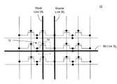
- FIG. 1Ashows a schematic representation of a semiconductor DRAM array including a plurality of memory cells in accordance with an embodiment of the present disclosure.
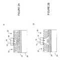
- FIG. 1Bshows a three-dimensional view of a memory cell in accordance with an embodiment of the present disclosure.
- FIG. 1Cshows a cross-sectional view along line C-C′ of the memory cell of FIG. 1B in accordance with an embodiment of the present disclosure.
- FIGS. 2A and 2Bshow a schematic charge relationship, for a given data state, of the floating body, source region, and drain regions of a memory cell in accordance with an embodiment of the present disclosure.
- FIGS. 3A and 3Bshow schematic block diagrams of embodiments of a semiconductor DRAM device including, memory cell arrays, data sense and write circuitry, memory cell selection, and control circuitry in accordance with an embodiment of the present disclosure.
- FIG. 4shows an exemplary embodiment of a memory array having a plurality of memory cells and employing a separate source line configuration for each row of memory cells in accordance with an embodiment of the present disclosure.
- FIG. 5shows a diagram of voltage control signals to implement a write operation for logic high or binary “1” data state into a memory cell in accordance with an embodiment of the present disclosure.
- FIG. 6shows a diagram of voltage control signals to implement a write operation for logic low or binary “0” data state into a memory cell in accordance with an embodiment of the present disclosure.
- FIG. 7shows a diagram of voltage control signals to implement a read operation of a memory cell in accordance with an embodiment of the present disclosure.
- FIG. 8shows control signal information (temporal and amplitude) to implement a read/write operation in accordance with an embodiment of the present disclosure.
- FIG. 9shows a schematic of a memory array implementing the structure and techniques having a common source line in accordance with an embodiment of the present disclosure.
- FIG. 10shows control signal information (temporal and amplitude) to implement a read/write operation in accordance with an embodiment of the present disclosure.
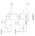
- FIG. 11shows a schematic circuit diagram of a voltage driver in accordance with an embodiment of the present disclosure.
- FIG. 12shows a diagram of voltage control signals to implement a write operation into a memory cell in accordance with an embodiment of the present disclosure.
- FIG. 13shows control signal information (temporal and amplitude) to implement a read/write operation in accordance with an embodiment of the present disclosure.
- the present disclosureis directed to a combination of reading/writing methods which allows relatively low power consumption and provides a relatively low voltage swing and thus reduces disruptions to unselected memory cells.
- a semiconductor DRAM device 10(e.g., a logic or discrete memory device) including one or more memory cells 12 including a memory transistor 14 having an electrically floating body (e.g., an N-channel type transistor or a P-channel type transistor).
- the memory transistor 14includes a source region 20 , a drain region 22 , a body region 18 disposed between the source region 20 and the drain region 22 , wherein the body region 18 is electrically floating, and a gate 16 disposed over the body region 18 .
- the body region 18may be disposed on or above region 24 , which may be an insulation region (e.g., in an SOT material/substrate) or non-conductive region (e.g., in a bulk-type material/substrate).
- region 24may be an insulation region (e.g., in an SOT material/substrate) or non-conductive region (e.g., in a bulk-type material/substrate).
- the insulation or non-conductive region 24may be disposed on substrate 26 .
- Datamay be written into a selected memory cell 12 by applying suitable control signals to a selected word line 28 , a selected source line 30 , and/or a selected bit line 32 .
- the memory cell 12may include (1) a first data state which is representative of a first amount of charges in the body region 18 of the memory transistor 14 , and (2) a second data state which is representative of a second amount of charges in the body region 18 of the memory transistor 14 .
- the semiconductor DRAM device 10may further include data write circuitry (not shown), coupled to the memory cell 12 , to apply (i) first write control signals to the memory cell 12 to write the first data state therein and (ii) second write control signals to the memory cell 12 to write the second data state therein, wherein, in response to the first write control signals applied to the memory cell 12 , the memory transistor 14 may generate a first bipolar transistor current which substantially provides the first charge in the body region 18 of the memory transistor 14 .
- charge carriersare accumulated in or emitted and/or ejected from electrically floating body region 18 wherein data states are defined by the amount of charge carriers accumulated within electrically floating body region 18 .
- the charge carriers accumulated on the electrically floating body 18may represent a logic high (binary “1” data state) or a logic low or (binary “0” data state).
- the first write control signalsmay include a signal applied to the gate 16 and a signal applied to the source region 20 wherein the signal applied to the source region 20 may include a first voltage potential having a first amplitude and a second voltage potential having a second amplitude.
- the first write control signalsmay include a signal applied to the gate 16 and a signal applied to the drain region 22 wherein the signal applied to the drain region 22 may include a first voltage potential having a first amplitude and a second voltage potential having a second amplitude.
- the second write signalsmay include a signal applied to the gate 16 , a signal applied to the source region 20 , and a signal applied to the drain region 22 .
- the signal applied to the drain region 22may include a block voltage to prevent the first data state from being written into the memory transistor 14 .
- the memory cell 12 of semiconductor DRAM device 10may operate by accumulating in or emitting/ejecting majority charge carriers 34 (e.g., electrons or holes) from the electrically floating body region 18 (e.g., N-Channel transistor illustrated in FIGS. 2A and 2B ).
- majority charge carriers 34e.g., electrons or holes
- various write techniquesmay be employed to accumulate majority charge carriers 34 (in this example, holes) in electrically floating body 18 of the memory cell 12 by, for example, impact ionization near source region 20 and/or drain region 22 (See, FIG. 2A ).
- the majority charge carriers 34may be emitted or ejected from the electrically floating body 18 by, for example, forward biasing the source region 20 /electrically floating body 18 junction and/or the drain region 22 /electrically floating body 18 junction (See, FIG. 2B ).
- a logic highmay correspond to, an increased concentration of majority charge carriers in the electrically floating body region 18 relative to an unwritten device and/or a device that is written with a logic low (binary data state “0”).
- a logic lowmay correspond to, for example, a reduced concentration of majority charge carriers in the electrically floating body region 18 relative to an unwritten device and/or a device that is written with a logic high (binary “1” data state).
- the semiconductor DRAM device 10may further include data sense circuitry (not shown), coupled to the memory cell 12 , to sense data state of the memory cell 12 .
- the memory transistor 14may generate a second bipolar transistor current which is representative of data state of the memory cell 12 and wherein the data sense circuitry may determine data state of the memory cell 12 at least substantially based on the second bipolar transistor current.
- the read control signalsmay include a signal applied to the gate 16 , source region 20 , and drain region 22 to cause, force and/or induce the bipolar transistor current which is representative of data state of the memory cell 12 .
- the signal applied to the drain region 22may include a positive voltage or a negative voltage. Indeed, one or more of the read control signals may include a constant or unchanging voltage amplitude.
- the semiconductor DRAM device 10may include a memory cell 12 array including a plurality of word lines (WL), a plurality of source lines (SL), a plurality of bit lines (BL), and a plurality of memory cells 12 arranged in a matrix of rows and columns.
- Each memory cell 12may include a memory transistor 14 , wherein the memory transistor 14 may include a source region 20 coupled to an associated source line (SL), a drain region 22 , a body region 18 disposed between the source region 20 , and the drain region 22 coupled to an associated bit line (BL) wherein the body region 18 is electrically floating, and a gate 16 disposed over the body region 18 and coupled to an associated word line (WL).
- the source region 20 of the memory transistor 14 of each memory cell 12 of a first row of memory cellsmay be connected to a first source line (SL).
- the source region 20 of the memory transistor 14 of each memory cell 12 of a second row of memory cellsis connected to the first source line (SL).
- the source region 20 of the memory transistor 14 of each memory cell 12 of a second row of memory cellsmay be connected to a second source line (SL)
- the source region 20 of the memory transistor 14 of each memory cell 12 of a third row of memory cellsis connected to a third source line (SL).
- FIGS. 3A and 3Bshow schematic block diagrams of a semiconductor DRAM device including, a memory cell array, data sense and write circuitry, memory cell selection and control circuitry in accordance with an embodiment of the present disclosure.
- the semiconductor DRAM device 10may include an array having a plurality of memory cells 12 having a separate source line (SL) for each row of memory cells (a row of memory cells includes a common word line connected to the gates 16 of each memory cell 12 of the row), data write and sense circuitry 36 , and memory cell selection and control circuitry 38 .
- the data write and sense circuitry 36may read data from and may write data to selected memory cells 12 .
- data write and sense circuitry 36may include a plurality of data sense amplifiers.
- Each data sense amplifiermay receive at least one bit line (BL) 32 and an output of reference generator circuitry (for example, a current or voltage reference signal).
- the data sense amplifiermay be a cross-coupled type sense amplifier to sense the data state stored in memory cell 12 and/or write-back data into memory cell 12 .
- the data sense amplifiermay employ voltage and/or current sensing circuitry and/or techniques.
- the data sense amplifiermay employ a current sensing circuitry and/or techniques, a current sense amplifier may compare the current from the selected memory cell 12 to a reference current, for example, the current of one or more reference cells. From that comparison, it may be determined whether memory cell 12 contained a logic high (binary “1” data state, relatively more majority charge carriers 34 contained within the body region 18 ) or a logic low (binary “0” data state, relatively less majority charge carriers 34 contained within the body region 18 ).
- any type or form of data write and sense circuitry 36(including one or more sense amplifiers, using voltage or current sensing techniques, to sense the data state stored in memory cell 12 ) to read the data stored in memory cells 12 and/or write data in memory cells 12 may be employed.
- memory cell selection and control circuitry 38may select and/or enable one or more predetermined memory cells 12 to facilitate reading data therefrom and/or writing data thereto by applying control signals on one or more word lines (WL) 28 and/or source lines (SL) 30 .
- the memory cell selection and control circuitry 38may generate such control signals using address data, for example, row address data.
- memory cell selection and control circuitry 38may include a word line decoder and/or driver.
- memory cell selection and control circuitry 38may include one or more different control/selection techniques (and circuitry therefor) to implement the memory cell selection technique. Such techniques, and circuitry therefor, are well known to those skilled in the art. Notably, all such control/selection techniques, and circuitry therefor, whether now known or later developed, are intended to fall within the scope of the present inventions.
- the semiconductor DRAM device 10may implement a two step write operation whereby all the memory cells 12 of a given row are written to a predetermined data state by first executing a “clear” operation, whereby all of the memory cells 12 of the given row are written to logic low (binary “0” data state), and thereafter selected memory cells 12 of the row are selectively written to the predetermined data state (here logic high (binary “1” data state)).
- the present disclosuremay also be implemented in conjunction with a one step write operation whereby selective memory cells of the selected row are selectively written to either logic high (binary “1” data state) or logic low (binary “0” data state) without first implementing a “clear” operation.
- the memory arraymay employ any of the exemplary writing, holding, and/or reading techniques described herein. Moreover, exemplary voltage values for each of the control signals for a given operation (for example, writing, holding or reading), according to exemplary embodiments of the present disclosure, is also provided.
- the memory transistors 14may be comprised of N-channel, P-channel and/or both types of transistors. Indeed, circuitry that is peripheral to the memory array (for example, sense amplifiers or comparators, row and column address decoders, as well as line drivers (not illustrated herein) may include P-channel and/or N-channel type transistors. Where P-channel type transistors are employed as memory cells 12 in the memory array(s), suitable write and read voltages (for example, negative voltages) are well known to those skilled in the art in light of this disclosure. Accordingly, for sake of brevity, these discussions will not be repeated.
- memory cells 12may be written using the two step operation wherein a given row of memory cells 12 are written to a first predetermined data state by first executing a “clear” operation (which, in this exemplary embodiment, a selected row 28 i and/or all of the memory cells 12 of the given row are written or programmed to logic low (binary “0” date state)) and thereafter selected memory cells 12 may be written to a second predetermined data state (i.e., a selective write operation to the second predetermined data state).
- the “clear” operationmay be performed by writing each memory cell 12 of the given row to a first predetermined data state (in this exemplary embodiment the first predetermined data state is logic low (binary “0” data state) using the inventive technique described above.
- memory transistor 14 of each memory cell 12 of a given rowis controlled to store a majority charge carrier concentration in the electrically floating body region 18 of the transistor 14 which corresponds to a logic low (binary “0” data state).
- control signals to implement a “clear” operationmay be applied to the gate 16 , the source region 20 , and the drain region 22 of the memory transistor 14 of memory cells 12 a - 12 d .
- a “clear operation”includes applying (i) 1.5V to the gate 16 , (ii) 0V to the source region 20 , and (iii) 0V to the drain region 22 of the memory transistor 14 .
- the same logic state(for example, logic low (binary “0” data state)) may be stored in memory cells 12 a - 12 d and the state of memory cells 12 a - 12 d may be “cleared”. For example, it may be preferable to maintain the gate-to-source voltage below the threshold voltage of the transistor of memory cell 12 to further minimize or reduce power consumption.
- selected memory cells 12 of a given rowmay be written to the second predetermined logic state.
- the memory transistors 14 of certain memory cells 12 of a given rowmay be written to the second predetermined logic state in order to store the second predetermined logic state in memory cells 12 .
- memory cells 12 b and 12 cmay be written to logic high (binary “1” data state) (as shown in a second selected row 28 i+1 ), via an impact ionization effect and/or avalanche multiplication, by applying (i) ⁇ 2.0V to the gate (via word line 28 i ), (ii) ⁇ 2.0V to the source region (via source line 30 i ), and (iii) 1.5V to the drain region (via bit line 32 j+1 and 32 j+2 ).
- control signalsmay generate or provide a bipolar current in the electrically floating body region 18 of the memory transistor 14 of memory cell 12 .
- the bipolar currentmay cause or produce impact ionization and/or the avalanche multiplication phenomenon in the electrically floating body region 18 of the memory transistors 14 of memory cells 12 b and 12 c . In this way, an excess of majority charge carriers may be provided and stored in the electrically floating body region 18 of the memory transistor 14 of memory cells 12 b and 12 c which corresponds to logic high (binary “1” data state).
- memory cells 12 a and 12 dmay be maintained at logic low (binary “0” data state) by applying a voltage to inhibit impact ionization to the drain region 22 of each memory cell 12 a and 12 d .
- applying 0V to the drain regions 22 of memory cells 12 a and 12 dmay inhibit impact ionization in memory cells 12 a and 12 d during the selective write operation for memory cells 12 b and 12 c.
- memory cells 12may be selectively written to logic high (binary “1” data state) using the band-to-band tunneling (GIDL) method.
- GIDLband-to-band tunneling
- the band-to-band tunnelingprovides, produces and/or generates an excess of majority charge carriers in the electrically floating body 18 of the memory transistors 14 of each selected memory cell 12 (in this exemplary embodiment, memory cells 12 b and 12 c ).
- memory cells 12 b and 12 cmay be written to logic high (binary “1” data state), via band-to-band tunneling, by applying (i) ⁇ 3V to the gate 16 (via word line 28 i ), (ii) ⁇ 0.5V to the source region 20 (via source line 30 i ), and (iii) 110V to the drain region 22 (via bit line 32 j+1 and 32 j+2 ).
- a selected row of memory cells 12may be read by applying a read control signals to the associated word line (WL) 28 and associated source lines (SL) 30 and sensing a signal (voltage and/or current) on associated bit lines (BL) 32 .
- memory cells 12 a - 12 d(e.g., as shown in a third selected row 28 i+3 ) may be read by applying (i) ⁇ 0.5V to the gate 16 (via word line 28 i ) and (ii) 3.0V to the source region 20 (via source line 30 i ).
- the data write and sense circuitry 36may read data state of the memory cells 12 a - 12 d by sensing the response to the read control signals applied to word line 28 i and source line 30 i .
- memory cells 12 a - 12 dmay generate a bipolar transistor current which may be representative of data state of memory cells 12 a - 12 d .
- memory cells 12 b and 12 cwhich were earlier written to logic high (binary “1” data state)
- memory cells 12 a and 12 dwhich were earlier programmed to logic low (binary “0” data state)
- such control signalsinduce, cause and/or produce little to no bipolar transistor current (for example, a considerable, substantial or sufficiently measurable bipolar transistor current).
- the circuitry in data write and sense circuitry 36 to sense the data state(for example, a cross-coupled sense amplifier) senses the data state using primarily and/or based substantially on the bipolar transistor current.
- the memory transistor 14 of each memory cell 12 a - 12 dmay generate a bipolar transistor current which is representative of the data state stored therein.
- the data sensing circuitry in data write and sense circuitry 36may determine data state of memory cells 12 a - 12 d based substantially on the bipolar transistor current induced, caused and/or produced in response to the read control signals.
- FIG. 5shows a diagram of voltage control signals to implement a write operation for logic high (binary “1” data state) into a memory cell 12 in accordance with an exemplary embodiment of the present disclosure.
- the control signalsmay be configured to provide a lower power consumption as well as a one step write whereby selective memory cells 12 of a selected row of memory cells 12 may be selectively written or programmed to either logic high (binary “1” data state) or logic low (binary “0” date state) without first implementing a “clear” operation.
- the temporally varying control signals to implement the write logic high (binary “1” data state) operationinclude the voltage applied to the gate 16 (V gw“1” ) and the voltage applied to the drain region 22 (V dw“1” ).
- the binary “1” or “0” data statesmay be written to one or more selected memory cells 12 by applying appropriate bit line voltages.
- the drain voltage (V dw“1”1 )may be applied to the drain region 22 (via, for example, the associated bit line) of the memory transistor 14 of the memory cell 12 before the gate voltage (V gw“1”1 ) may be applied to the gate 16 (via, for example, the associated word line), simultaneously thereto, or after the gate voltage (V gw“1”1 ) is applied to gate 16 .
- the drain voltage (V dw“1”1 )include an amplitude which may be sufficient to maintain a bipolar current that is suitable for programming the memory cell 12 to logic high (binary “1” data state).
- the drain voltage (V dw“1”1 )extend beyond/after or continue beyond the conclusion of the gate voltage (V gw“1”1 ), or extend beyond/after or continue beyond the time the gate voltage (V gw“1”1 ) is reduced, as illustrated in FIG. 5 (see, ⁇ t>0). Therefore, majority charge carriers may be generated in the electrically floating body region 18 via a bipolar current and majority charge carriers may accumulate (and be stored) in a portion of the electrically floating body region 18 of the memory transistor 14 of the memory cell 12 that may be juxtaposed or near the gate dielectric (which is disposed between the gate 16 and the electrically floating body region 18 ).
- the gate voltage (V gw“1”2 )may be equal to (or substantially equal to) the voltage applied to the gate 16 to implement a hold operation (V gh ) and the drain bias (V dw“1”2 ) may be equal to (or substantially equal to) the voltage applied to the drain region to implement a hold operation (V dh ).
- FIG. 6shows a diagram of voltage control signals to implement a write operation for logic low (binary “0” data state) into a memory cell in accordance with an embodiment of the present disclosure.
- the temporally varying control signals that may be implemented to write logic low (binary “0” data state)may include the voltage applied to the gate 16 (V gw“0” ) and the voltage applied to the drain region 22 (V dw“0” ).
- the control signal applied to the drain region 22(V dw“0”1 ) may be applied before the control signal is applied to the gate 16 (V gw“0”1 ), or simultaneously thereto, or after the control signal is applied to the gate 16 .
- the drain voltage (V dw“0”1 )may include an amplitude which may be insufficient to maintain a bipolar current that is suitable for writing the memory cell 12 to logic high (binary “1” data state). From a relative timing perspective, it may be preferred that the drain voltage (V dw“0”1 ) extend beyond/after or continue beyond the conclusion of the gate voltage (V gw“0”1 ), or extend beyond/after or continue beyond the time the gate voltage (V gw“0”1 ) is reduced, as illustrated in FIG. 6 (see, ⁇ t>0).
- majority charge carriersmay be generated in the electrically floating body region 18 via a bipolar current and majority charge carriers may be accumulated (and be stored) in a portion of the electrically floating body region 18 of the memory transistor 14 of the memory cell 12 that is juxtaposed or near the gate dielectric (which is disposed between the gate 16 and the electrically floating body region 18 ).
- the gate voltage (V gw“0”2 )may be equal to (or substantially equal to) the voltage applied to the gate 16 to implement a hold operation (V gh ) and the drain bias (V dw“0”2 ) may be equal to (or substantially equal to) the voltage applied to the drain region 22 to implement a hold operation (V dh ).
- FIG. 7shows a diagram of voltage control signals to implement a read operation of a memory cell in accordance with an embodiment of the present disclosure.
- read control signalsmay be applied to the drain region 22 and the gate 16 .
- the voltage applied to the drain region 22 (V dr )may be applied to drain region 22 before application of the voltage applied to the gate 16 (V gr ), simultaneously thereto, or after the voltage is applied to the gate 16 .
- the drain voltage (V dr )may cease or terminate before the gate voltage (V gr ), simultaneously thereto (as illustrated in FIG. 7 ), or after the gate voltage (V gr ) may conclude or cease.
- a bipolar currentis generated in memory cells 12 storing logic high (binary “1” data state) and little to no bipolar current is generated in memory cells 12 storing logic low (binary “0” data state).
- the data statemay be determined primarily by, sensed substantially using and/or based substantially on the bipolar transistor current that is responsive to the read control signals and significantly less by the interface channel current component, which is less significant and/or negligible relatively to the bipolar component.
- the writing and reading techniques described hereinmay be employed in conjunction with a plurality of memory cells 12 arranged in an array of memory cells.
- a memory array implementing the structure and techniques of the present inventionsmay be controlled and configured including a plurality of memory cells 12 having a separate source line (SL) for each row of memory cells 12 (a row of memory cells includes a common word line).
- SLsource line
- the exemplary layouts or configurations (including exemplary control signal voltage values), in accordance to one or more exemplary embodiments of the present disclosureare shown, each consisting of the control signal waveforms and exemplary array voltages during one-step writing phase 1 , phase 2 , and reading.
- the temporally varying control signals to implement a write operationmay include (i) a voltage applied to the gate 16 (V gw ) via the associated word line (WL), (ii) a voltage applied to the source region 20 (V sw ) via the source line (SL), and (iii) a voltage applied to the drain region 22 (V dw ) via the associated bit line (BL).
- the binary “1” or “0” data statesmay be written to one or more selected memory cells 12 by applying appropriate bit line voltages.
- logic highmay be written into a memory cell 12 by applying drain voltage (V dw“1” ) having an amplitude of 0.5V
- logic lowmay be written into a memory cell 12 by applying the drain voltage (V dw“0” ) having an amplitude of 0V
- the source voltage (V sw1 )may include an amplitude of ⁇ 2.5V
- the gate voltage (V gw1 )may include an amplitude of 2.5V.
- the source voltage (V sw2 )may include an amplitude of ⁇ 2.2V and the gate voltage (V gw2 ) may include an amplitude of ⁇ 3.3V.
- V sw2the source voltage
- V gw2the gate voltage
- V gw2the gate voltage
- a bipolar current that is suitable for writing the memory cell 12 to logic high (binary “1” data state)may be provided.
- little to no bipolar currentis generated for writing the memory cell to logic low (binary “0” data state).
- a row of memory cellsmay be read in series and/or in parallel.
- memory cells 12are read by applying the following read control signals: (i) a voltage applied to the gate 16 (V gr ) via the associated word line (WL) and (ii) a voltage applied to the source (V sr ) via the source line (SL).
- the logic state of each memory cell(e.g., 12 a - 12 d ) may be sensed, determined and/or sampled on the associated bit line (BL) ( 32 j - 32 j+3 , respectively).
- the gate voltage (V gr )may include an amplitude of 0.5V
- the source voltage (V sr )may include an amplitude of 3.0V.
- a bipolar currentmay be generated in memory cells 12 storing logic high (binary “1” data state) and little to no bipolar current may be generated in memory cells 12 storing logic low (binary “1” data state).
- the data statemay be determined primarily by, sensed substantially using and/or based substantially on the bipolar transistor current that is responsive to the read control signals and significantly less by the interface channel current component, which is less significant and/or negligible relatively to the bipolar component.
- each voltage levelmay be increased or decreased by a given voltage amount (e.g., each voltage may be increased or decreased by 0.5V, 1.0V and 2.0V) whether one or more of the voltages (e.g., the source region voltage, the drain region voltage or gate voltage) become or are positive and negative.
- a given voltage amounte.g., each voltage may be increased or decreased by 0.5V, 1.0V and 2.0V
- FIGS. 9 and 10show a schematic of a memory array implementing the structure and techniques having a common source line (SL) in accordance with an exemplary embodiment of the present disclosure.
- the present disclosuremay be implemented in any memory array architecture having a plurality of memory cells that employ memory transistors.
- a memory array implementing the structure and techniques of the present disclosuremay be controlled and configured having a common source line (SL) for every two rows of memory cells 12 (a row of memory cells 12 includes a common word line (WL)).
- An example (including exemplary control signal voltage values)may be also shown that consists of the control signal waveforms and exemplary array voltages during one-step writing phase 1 , phase 2 , and reading.
- the temporally varying control signals to implement the write operationmay include (i) a voltage applied to the gate (V gw ) via the associated word line (WL) and (ii) a voltage applied to the drain region (V dw ) via the associated bit line (BL).
- the binary “1” or “0” data statesmay be written to one or more selected memory cells 12 by applying appropriate bit line voltages. Thereby, logic high (binary “1” data state) may be written into a memory cell 12 by applying drain voltage (V dw“1” ) having (i) an amplitude of 3V during phase 1 and (ii) an amplitude of 2.7V during phase 2 .
- logic lowmay be written into a memory cell by applying the drain voltage (V dw“0” ) having (i) an amplitude of 2.5V during phase 1 and (ii) an amplitude of 2.2V during phase 2 .
- the gate voltage (V gw1 )may include an amplitude of 0V.
- the gate voltage (V gw2 )may include an amplitude of ⁇ 1.5V.
- the voltage applied to the source lines (SL)(and, as such, the source regions 20 of the memory transistors 14 of the row of memory cells 12 ) may be 0V. Under these conditions, a bipolar current that may be suitable for writing the memory cell to logic high (binary “1” data state) is provided. Moreover, little to no bipolar current is generated for programming the memory cell to logic low (binary “0” data state).
- a row of memory cellsmay be read in series and/or parallel.
- the memory cells 12may be read by applying the following read control signals: (i) a voltage applied to the gate (V gr ) via the associated word line (WL) and (ii) a voltage applied to the drain (V dr ) via the associated bit line (BL).
- the logic state of each memory cell 12(for example, 12 a - 12 d ) is sensed, determined, and/or sampled on the associated bit line (BL) ( 32 j - 32 j+3 , respectively).
- the gate voltage (V gr )may include an amplitude of ⁇ 0.5V and the drain voltage (V dr ) may include an amplitude of 3V.
- the voltage applied to the source lines (SL)(and, as such, the source regions 20 of the memory transistors 14 of the row of memory cells 12 ) is 0V.
- a bipolar currentmay be generated in those memory cells 12 storing logic high (binary “1” data state) and little to no bipolar current may be generated in those memory cells 12 storing logic low (binary “0” data state).
- the data statemay be determined primarily by, sensed substantially using, and/or based substantially on the bipolar transistor current that is responsive to the read control signals and significantly less by the interface channel current component, which may be less significant and/or negligible relatively to the bipolar component.
- de-selected memory cells 12e.g., idle memory cells 12
- memory cell arrayit may be advantageous to employ a “holding” operation or condition for de-selected memory cells 12 (e.g., idle memory cells 12 ) in memory cell array to minimize and/or reduce the impact of the write/read operations for selected memory cells 12 (e.g., memory cells 12 being written to and/or read from) connected to word lines 28 i , 28 i+1 , 28 i+2 , 28 i+3 and 28 i+4 .
- a holding voltagemay be applied to the gates 16 of the memory transistors 14 of the de-selected memory cells 12 of memory cell array 10 (for example, memory cells 12 connected to word lines 28 i+1 , 28 i+2 , 28 i+3 , and 28 i+4 ).
- a holding voltage applied to the de-selected memory cells 12may be approximate to an operation voltage applied to the selected memory cells 12 to perform the write/read operations. By applying a holding voltage approximate to an operation voltage for performing the write/read operations, the voltage swing between the holding voltage and the operation voltage may be reduced.
- a power consumptionmay be reduced because (i) only voltage applied to selected bit lines (e.g., associated with the selected memory cells 12 ) may be varied, and (ii) the source line voltage swing (e.g., between holding condition and write/read operations) may be reduced.
- a circuit sizemay be reduced, for example, reducing one or more components (e.g., reduce a number of transistors cascoded in series) for a source line driver.
- FIG. 11shows a schematic diagram of a voltage driver 110 in accordance with an embodiment of the present disclosure.
- the voltage driver 110may be arranged in an inverter circuit configuration and/or other circuit configurations having one or more transistors cascoded in series for generating one or more voltage potentials.
- a ground (VSS)may be coupled to the voltage driver 110 .
- the ground (VSS)may be held at 0V during a holding operation or condition.
- the voltage swing between the holding voltage and the operation voltagemay be reduced by raising the voltage applied to the switch low supply (VSLHD) to a higher voltage (e.g., VSLHD>0V) or a voltage potential similar to the operation voltage.
- VSLHDswitch low supply
- the voltage driver 110may apply a holding voltage approximately in a range of 0.5V to 1.5V to the source region 20 and/or drain region 22 of each memory transistor 14 of the one or more de-selected memory cells 12 connected to word lines (WL) 28 i+1 , 28 i+2 , 28 i+3 , and 28 i+4 .
- FIG. 12shows a diagram of voltage control signals to implement a program or write operation into a memory cell in accordance with an embodiment of the present disclosure.
- the control signalsmay be configured to provide a low voltage swing between a holding operation or condition and/or a write operation and thus lower power consumption as well.
- the temporally varying control signals to implement the write operationmay include a voltage applied to the source region 20 (V sw ) a voltage applied to the gate (V gw ) and a voltage applied to the drain region 22 (V dw ).
- the binary “1” or “0” data statesmay be written to one or more selected memory cells 12 by applying appropriate bit line voltages.
- a voltage swing between a holding voltage and a writing voltagemay be reduced by raising the holding voltage and thus reducing power consumption.
- a voltage applied to the source line (SL) and a voltage applied to the bit line (BL)may be the same as the voltage applied during a write operation in order to reduce the voltage swing.
- the voltage applied to the source line (SL) and the voltage applied to the bit line (BL)may be 0.5V.
- a voltagemay be in the range of ⁇ 0.2V to ⁇ 1.8V and applied to the word line (WL).
- the control signal applied to the drain region 22may be applied before the control signal is applied to the gate 16 (V gw“0” ), or simultaneously thereto, or after the control signal is applied to the gate 16 .
- the voltage swing between the control signal applied to the drain region 22 during the write operation and the control signal applied during the holding voltagemay be reduced.
- the drain voltage (V dw“0” )may include an amplitude which is insufficient to maintain a bipolar current that is suitable for writing the memory cell to logic high (binary “1” data state).
- the drain voltage (V dw“0”1 )extend beyond/after or continue beyond the conclusion of the gate voltage (V gw“0”1 ), or extend beyond/after or continue beyond the time the gate voltage (V gw“0”1 ) is reduced, as illustrated in FIG. 12 .
- majority charge carriersmay be generated in the electrically floating body region 18 via a bipolar current and majority charge carriers may accumulate (and be stored) in a portion of the electrically floating body region 18 of the memory transistor 14 of the memory cell 12 that is juxtaposed or near the gate dielectric (which is disposed between the gate 16 and the electrically floating body region 18 ).
- the drain voltage (V dw“1” )may be applied to the drain region 22 (via, for example, the associated bit line (BL)) of the memory transistor 14 of the memory cell 12 before the gate voltage (V gw“1” ) may be applied to the gate 16 (via, for example, the associated word line), simultaneously thereto, or after the gate voltage (V gw“1” ) is applied to gate 16 .
- the holding voltageat 0.5V, the voltage swing between the control signal applied to the drain region 22 during the writing operation and the control signal applied during the holding voltage may be reduced.
- the drain voltage (V dw“1” )include an amplitude which may be sufficient to maintain a bipolar current that is suitable for programming the memory cell 12 to logic high (binary “1” data state). From a relative timing perspective, it is preferred that the drain voltage (V dw“1” ) extend beyond/after or continue beyond the conclusion of the gate voltage (V gw“1” ), or extend beyond/after or continue beyond the time the gate voltage (V gw“1” ) is reduced.
- majority charge carriersmay be generated in the electrically floating body region 18 via a bipolar current and majority charge carriers may be accumulated (and be stored) in a portion of the electrically floating body region 18 of the memory transistor 14 of the memory cell 12 that may be juxtaposed or near the gate dielectric (which is disposed between the gate 16 and the electrically floating body region 18 ).
- the drain voltage (V dw“msk” )may be applied to the drain region 22 (via, for example, the associated bit line) of the memory transistor 14 of the memory cell 12 before the gate voltage (V gw“1” ) may be applied to the gate 16 (via, for example, the associated word line), simultaneously thereto, or after the gate voltage (V gw“1” ) is applied to gate 16 .
- the holding voltageat 0.5V, the voltage swing between the control signal applied to the drain region 22 during the mask writing operation and control signal applied during the holding voltage may be reduced.
- the temporally varying control signals to implement a holding operation or conditionmay include (i) a voltage applied to the gate 16 via the associated word line (VWL HD ), (ii) a voltage applied to the source region 20 via the source line (VSL HD ), and (iii) a voltage applied to the drain region 22 via the associated bit line (VBL HD ).
- a holding voltage applied to the word line (VWL HD )may be ⁇ 1.2V
- a holding voltage applied to the source line (VSL HD )may be 1.1V
- a holding voltage applied to the bit line (VBL HD )may be 1.1V.
- the temporally varying control signals to implement a write operationmay include (i) a voltage applied to the gate 16 via the associated word line (VWL WR ), (ii) a voltage applied to the source region 20 via the source line (VSL WR ), and (iii) a voltage applied to the drain region 22 via the associated bit line (VBL WR ).
- binary “1” or “0” data statesmay be written to one or more selected memory cells 12 by applying appropriate bit line voltages.
- logic highmay be written into a memory cell 12 by applying drain voltage (VBL WR“1” ) having an amplitude of 0.0V
- logic lowmay be written into a memory cell 12 by applying the drain voltage (VBL WR“0” ) having an amplitude of 0.5V
- a mask writing operationmay be employed by applying an appropriate bit line voltage (VBLMSK WR ).
- VBLMSK WRbit line voltage
- a mask voltage applied to the bit line (VBLMSK WR )may be 1.1V.
- the voltage applied to the source voltage (VSL)may include an amplitude of 2.5V and the gate voltage (VWL WR ) may include an amplitude of 0.3V.
- a control voltagemay be applied to the word line (VWL MID ) in order to control a writing operation (e.g., writing a logic “1”).
- the control voltage applied to the word line (VWL MID )may be approximately ⁇ 0.9V.
- the temporally varying control signals to implement a read operationmay include (i) a voltage applied to the gate 16 via the associated word line (VWL RD ), (ii) a voltage applied to the source region 20 via the source line (VSL RD ), and (iii) a voltage applied to the drain region 22 via the associated bit line (VBL RD ).
- a row of memory cellse.g., 12 a - 12 d
- the logic state of each memory cell(e.g., 12 a - 12 d ) may be sensed, determined, and/or sampled on the associated bit line ( 32 j - 32 j+3 , respectively).
- the gate voltage (VWL RD )may include an amplitude of 0.5V
- the source voltage (VSL RD )may include an amplitude of 2.5V
- the drain voltage (VBL RD )may include an amplitude of 0V.
- a mask read operationmay be executed by applying a drain voltage (VBLMSK RD ) of approximately 1.1V.
- FIG. 13also illustrates a voltage applied to a word line (VWL GDL ) in order to reduce band-to-band tunneling (gate-induced drain leakage “GIDL”), as described above.
- VWL GDLvoltage applied to a word line
- GIDLgate-induced drain leakage
- each voltage levelmay be increased or decreased by a given voltage amount (e.g., each voltage may be increased or decreased by 0.5V, 1.0V and 2.0V) whether one or more of the voltages (e.g., the source region voltage, the drain region voltage or gate voltage) become or are positive and negative.
- a given voltage amounte.g., each voltage may be increased or decreased by 0.5V, 1.0V and 2.0V
- reducing a voltage swing in accordance with the present disclosure as described abovetypically involves the processing of input data and the generation of output data to some extent.
- This input data processing and output data generationmay be implemented in hardware or software.
- specific electronic componentsmay be employed in a semiconductor DRAM device or similar or related circuitry for implementing the functions associated with reducing a voltage swing in accordance with the present disclosure as described above.
- one or more processors operating in accordance with instructionsmay implement the functions associated with reducing a voltage swing in accordance with the present disclosure as described above.
- Such instructionsmay be stored on one or more processor readable media (e.g., a magnetic disk or other storage medium), or transmitted to one or more processors via one or more signals embodied in one or more carrier waves.
- processor readable mediae.g., a magnetic disk or other storage medium
Landscapes
- Engineering & Computer Science (AREA)
- Microelectronics & Electronic Packaging (AREA)
- Computer Hardware Design (AREA)
- Semiconductor Memories (AREA)
- Dram (AREA)
Abstract
Description
Claims (28)
Priority Applications (2)
| Application Number | Priority Date | Filing Date | Title |
|---|---|---|---|
| US12/244,183US7933140B2 (en) | 2008-10-02 | 2008-10-02 | Techniques for reducing a voltage swing |
| US13/092,673US8315083B2 (en) | 2008-10-02 | 2011-04-22 | Techniques for reducing a voltage swing |
Applications Claiming Priority (1)
| Application Number | Priority Date | Filing Date | Title |
|---|---|---|---|
| US12/244,183US7933140B2 (en) | 2008-10-02 | 2008-10-02 | Techniques for reducing a voltage swing |
Related Child Applications (1)
| Application Number | Title | Priority Date | Filing Date |
|---|---|---|---|
| US13/092,673ContinuationUS8315083B2 (en) | 2008-10-02 | 2011-04-22 | Techniques for reducing a voltage swing |
Publications (2)
| Publication Number | Publication Date |
|---|---|
| US20100085806A1 US20100085806A1 (en) | 2010-04-08 |
| US7933140B2true US7933140B2 (en) | 2011-04-26 |
Family
ID=42075700
Family Applications (2)
| Application Number | Title | Priority Date | Filing Date |
|---|---|---|---|
| US12/244,183Active2029-08-08US7933140B2 (en) | 2008-10-02 | 2008-10-02 | Techniques for reducing a voltage swing |
| US13/092,673ActiveUS8315083B2 (en) | 2008-10-02 | 2011-04-22 | Techniques for reducing a voltage swing |
Family Applications After (1)
| Application Number | Title | Priority Date | Filing Date |
|---|---|---|---|
| US13/092,673ActiveUS8315083B2 (en) | 2008-10-02 | 2011-04-22 | Techniques for reducing a voltage swing |
Country Status (1)
| Country | Link |
|---|---|
| US (2) | US7933140B2 (en) |
Cited By (51)
| Publication number | Priority date | Publication date | Assignee | Title |
|---|---|---|---|---|
| US20100034041A1 (en)* | 2008-08-05 | 2010-02-11 | Yuniarto Widjaja | Method of operating semiconductor memory device with floating body transistor using silicon controlled rectifier principle |
| US8514622B2 (en) | 2007-11-29 | 2013-08-20 | Zeno Semiconductor, Inc. | Compact semiconductor memory device having reduced number of contacts, methods of operating and methods of making |
| US8514623B2 (en) | 2007-11-29 | 2013-08-20 | Zeno Semiconductor, Inc. | Method of maintaining the state of semiconductor memory having electrically floating body transistor |
| US8547756B2 (en) | 2010-10-04 | 2013-10-01 | Zeno Semiconductor, Inc. | Semiconductor memory device having an electrically floating body transistor |
| US8570803B2 (en) | 2006-11-29 | 2013-10-29 | Zeno Semiconductor, Inc. | Semiconductor memory having both volatile and non-volatile functionality and method of operating |
| US8582359B2 (en) | 2010-11-16 | 2013-11-12 | Zeno Semiconductor, Inc. | Dual-port semiconductor memory and first-in first-out (FIFO) memory having electrically floating body transistor |
| US8957458B2 (en) | 2011-03-24 | 2015-02-17 | Zeno Semiconductor, Inc. | Asymmetric semiconductor memory device having electrically floating body transistor |
| US9025358B2 (en) | 2011-10-13 | 2015-05-05 | Zeno Semiconductor Inc | Semiconductor memory having both volatile and non-volatile functionality comprising resistive change material and method of operating |
| US9029922B2 (en) | 2013-03-09 | 2015-05-12 | Zeno Semiconductor, Inc. | Memory device comprising electrically floating body transistor |
| US9153309B2 (en) | 2010-02-07 | 2015-10-06 | Zeno Semiconductor Inc. | Semiconductor memory device having electrically floating body transistor, semiconductor memory device having both volatile and non-volatile functionality and method or operating |
| US9208880B2 (en) | 2013-01-14 | 2015-12-08 | Zeno Semiconductor, Inc. | Content addressable memory device having electrically floating body transistor |
| US9230651B2 (en) | 2012-04-08 | 2016-01-05 | Zeno Semiconductor, Inc. | Memory device having electrically floating body transitor |
| US9275723B2 (en) | 2013-04-10 | 2016-03-01 | Zeno Semiconductor, Inc. | Scalable floating body memory cell for memory compilers and method of using floating body memories with memory compilers |
| US9281022B2 (en) | 2013-07-10 | 2016-03-08 | Zeno Semiconductor, Inc. | Systems and methods for reducing standby power in floating body memory devices |
| US9368625B2 (en) | 2013-05-01 | 2016-06-14 | Zeno Semiconductor, Inc. | NAND string utilizing floating body memory cell |
| US9391079B2 (en) | 2007-11-29 | 2016-07-12 | Zeno Semiconductor, Inc. | Compact semiconductor memory device having reduced number of contacts, methods of operating and methods of making |
| US9496053B2 (en) | 2014-08-15 | 2016-11-15 | Zeno Semiconductor, Inc. | Memory device comprising electrically floating body transistor |
| US9548119B2 (en) | 2014-01-15 | 2017-01-17 | Zeno Semiconductor, Inc | Memory device comprising an electrically floating body transistor |
| US9601493B2 (en) | 2006-11-29 | 2017-03-21 | Zeno Semiconductor, Inc | Compact semiconductor memory device having reduced number of contacts, methods of operating and methods of making |
| US9922981B2 (en) | 2010-03-02 | 2018-03-20 | Zeno Semiconductor, Inc. | Compact semiconductor memory device having reduced number of contacts, methods of operating and methods of making |
| US10079301B2 (en) | 2016-11-01 | 2018-09-18 | Zeno Semiconductor, Inc. | Memory device comprising an electrically floating body transistor and methods of using |
| US10340276B2 (en) | 2010-03-02 | 2019-07-02 | Zeno Semiconductor, Inc. | Method of maintaining the state of semiconductor memory having electrically floating body transistor |
| US10447274B2 (en) | 2017-07-11 | 2019-10-15 | iCometrue Company Ltd. | Logic drive based on standard commodity FPGA IC chips using non-volatile memory cells |
| US10461084B2 (en) | 2010-03-02 | 2019-10-29 | Zeno Semiconductor, Inc. | Compact semiconductor memory device having reduced number of contacts, methods of operating and methods of making |
| US10489544B2 (en) | 2016-12-14 | 2019-11-26 | iCometrue Company Ltd. | Logic drive based on standard commodity FPGA IC chips |
| US10523210B2 (en) | 2018-02-01 | 2019-12-31 | iCometrue Company Ltd. | Logic drive using standard commodity programmable logic IC chips comprising non-volatile random access memory cells |
| US10553683B2 (en) | 2015-04-29 | 2020-02-04 | Zeno Semiconductor, Inc. | MOSFET and memory cell having improved drain current through back bias application |
| US10608638B2 (en) | 2018-05-24 | 2020-03-31 | iCometrue Company Ltd. | Logic drive using standard commodity programmable logic IC chips |
| US10623000B2 (en) | 2018-02-14 | 2020-04-14 | iCometrue Company Ltd. | Logic drive using standard commodity programmable logic IC chips |
| US10630296B2 (en) | 2017-09-12 | 2020-04-21 | iCometrue Company Ltd. | Logic drive with brain-like elasticity and integrality based on standard commodity FPGA IC chips using non-volatile memory cells |
| US10892011B2 (en) | 2018-09-11 | 2021-01-12 | iCometrue Company Ltd. | Logic drive using standard commodity programmable logic IC chips comprising non-volatile random access memory cells |
| US10937762B2 (en) | 2018-10-04 | 2021-03-02 | iCometrue Company Ltd. | Logic drive based on multichip package using interconnection bridge |
| US10957679B2 (en) | 2017-08-08 | 2021-03-23 | iCometrue Company Ltd. | Logic drive based on standardized commodity programmable logic semiconductor IC chips |
| US10985154B2 (en) | 2019-07-02 | 2021-04-20 | iCometrue Company Ltd. | Logic drive based on multichip package comprising standard commodity FPGA IC chip with cryptography circuits |
| US11201215B2 (en) | 2015-04-29 | 2021-12-14 | Zeno Semiconductor, Inc. | MOSFET and memory cell having improved drain current through back bias application |
| US11211334B2 (en) | 2018-11-18 | 2021-12-28 | iCometrue Company Ltd. | Logic drive based on chip scale package comprising standardized commodity programmable logic IC chip and memory IC chip |
| US11227838B2 (en) | 2019-07-02 | 2022-01-18 | iCometrue Company Ltd. | Logic drive based on multichip package comprising standard commodity FPGA IC chip with cooperating or supporting circuits |
| US11309334B2 (en) | 2018-09-11 | 2022-04-19 | iCometrue Company Ltd. | Logic drive using standard commodity programmable logic IC chips comprising non-volatile random access memory cells |
| US11404419B2 (en) | 2018-04-18 | 2022-08-02 | Zeno Semiconductor, Inc. | Memory device comprising an electrically floating body transistor |
| US11600526B2 (en) | 2020-01-22 | 2023-03-07 | iCometrue Company Ltd. | Chip package based on through-silicon-via connector and silicon interconnection bridge |
| US11600663B2 (en) | 2019-01-11 | 2023-03-07 | Zeno Semiconductor, Inc. | Memory cell and memory array select transistor |
| US11616046B2 (en) | 2018-11-02 | 2023-03-28 | iCometrue Company Ltd. | Logic drive based on chip scale package comprising standardized commodity programmable logic IC chip and memory IC chip |
| US11625523B2 (en) | 2016-12-14 | 2023-04-11 | iCometrue Company Ltd. | Logic drive based on standard commodity FPGA IC chips |
| US11637056B2 (en) | 2019-09-20 | 2023-04-25 | iCometrue Company Ltd. | 3D chip package based on through-silicon-via interconnection elevator |
| US11887930B2 (en) | 2019-08-05 | 2024-01-30 | iCometrue Company Ltd. | Vertical interconnect elevator based on through silicon vias |
| US11908899B2 (en) | 2009-02-20 | 2024-02-20 | Zeno Semiconductor, Inc. | MOSFET and memory cell having improved drain current through back bias application |
| US11974425B2 (en) | 2012-02-16 | 2024-04-30 | Zeno Semiconductor, Inc. | Memory cell comprising first and second transistors and methods of operating |
| US12176278B2 (en) | 2021-05-30 | 2024-12-24 | iCometrue Company Ltd. | 3D chip package based on vertical-through-via connector |
| US12268012B2 (en) | 2021-09-24 | 2025-04-01 | iCometrue Company Ltd. | Multi-output look-up table (LUT) for use in coarse-grained field-programmable-gate-array (FPGA) integrated-circuit (IC) chip |
| US12283599B2 (en)* | 2009-12-25 | 2025-04-22 | Semiconductor Energy Laboratory Co., Ltd. | Semiconductor device |
| US12439611B2 (en) | 2019-03-12 | 2025-10-07 | Zeno Semiconductor, Inc. | Memory cell and memory array select transistor |
Families Citing this family (9)
| Publication number | Priority date | Publication date | Assignee | Title |
|---|---|---|---|---|
| KR101497542B1 (en)* | 2008-10-21 | 2015-03-02 | 삼성전자주식회사 | Operation method of semiconductor device |
| US9007866B2 (en)* | 2013-04-23 | 2015-04-14 | Tessera Inc. | Retention optimized memory device using predictive data inversion |
| US9196357B2 (en) | 2013-12-20 | 2015-11-24 | Micron Technology, Inc. | Voltage stabilizing for a memory cell array |
| US9704585B2 (en) | 2015-06-15 | 2017-07-11 | Cypress Semiconductor Corporation | High voltage architecture for non-volatile memory |
| US11189331B1 (en) | 2020-07-15 | 2021-11-30 | Ferroelectric Memory Gmbh | Memory cell arrangement and methods thereof |
| US11081159B1 (en)* | 2020-07-15 | 2021-08-03 | Ferroelectric Memory Gmbh | Memory cell arrangement and methods thereof |
| US20220139934A1 (en) | 2020-10-30 | 2022-05-05 | Ferroelectric Memory Gmbh | Memory cell, capacitive memory structure, and methods thereof |
| US11950430B2 (en) | 2020-10-30 | 2024-04-02 | Ferroelectric Memory Gmbh | Memory cell, capacitive memory structure, and methods thereof |
| JP7566676B2 (en)* | 2021-03-22 | 2024-10-15 | キオクシア株式会社 | MEMORY SYSTEM AND INFORMATION PROCESSING SYSTEM |
Citations (295)
| Publication number | Priority date | Publication date | Assignee | Title |
|---|---|---|---|---|
| CA272437A (en) | 1925-10-22 | 1927-07-19 | Edgar Lilienfeld Julius | Electric current control mechanism |
| US3439214A (en) | 1968-03-04 | 1969-04-15 | Fairchild Camera Instr Co | Beam-junction scan converter |
| FR2197494A5 (en) | 1972-08-25 | 1974-03-22 | Radiotechnique Compelec | |
| GB1414228A (en) | 1972-04-25 | 1975-11-19 | Ibm | Semiconductor storage devices |
| US3997799A (en) | 1975-09-15 | 1976-12-14 | Baker Roger T | Semiconductor-device for the storage of binary data |
| US4032947A (en) | 1971-10-20 | 1977-06-28 | Siemens Aktiengesellschaft | Controllable charge-coupled semiconductor device |
| US4250569A (en) | 1978-11-15 | 1981-02-10 | Fujitsu Limited | Semiconductor memory device |
| US4262340A (en) | 1978-11-14 | 1981-04-14 | Fujitsu Limited | Semiconductor memory device |
| US4298962A (en) | 1979-01-25 | 1981-11-03 | Nippon Electric Co., Ltd. | Memory |
| US4371955A (en) | 1979-02-22 | 1983-02-01 | Fujitsu Limited | Charge-pumping MOS FET memory device |
| EP0030856B1 (en) | 1979-12-13 | 1984-03-21 | Fujitsu Limited | Charge-pumping semiconductor memory cell comprising a charge-storage region and memory device using such a cell |
| US4527181A (en) | 1980-08-28 | 1985-07-02 | Fujitsu Limited | High density semiconductor memory array and method of making same |
| US4630089A (en) | 1983-09-27 | 1986-12-16 | Fujitsu Limited | Semiconductor memory device |
| US4658377A (en) | 1984-07-26 | 1987-04-14 | Texas Instruments Incorporated | Dynamic memory array with segmented bit lines |
| US4791610A (en) | 1985-05-24 | 1988-12-13 | Fujitsu Limited | Semiconductor memory device formed of a SOI-type transistor and a capacitor |
| US4807195A (en) | 1987-05-18 | 1989-02-21 | International Business Machines Corporation | Apparatus and method for providing a dual sense amplifier with divided bit line isolation |
| EP0354348A2 (en) | 1988-08-10 | 1990-02-14 | International Business Machines Corporation | CMOS-transistor and one-capacitor dram cell and fabrication process therefor |
| US4954989A (en) | 1988-04-12 | 1990-09-04 | Commissariat A L'energie Atomique | MIS type static memory cell and memory and storage process |
| US4979014A (en) | 1987-08-10 | 1990-12-18 | Kabushiki Kaisha Toshiba | MOS transistor |
| EP0202515B1 (en) | 1982-11-04 | 1991-03-13 | Hitachi, Ltd. | Semiconductor memory |
| US5010524A (en) | 1989-04-20 | 1991-04-23 | International Business Machines Corporation | Crosstalk-shielded-bit-line dram |
| EP0175378B1 (en) | 1984-09-21 | 1991-11-21 | Fujitsu Limited | Dynamic random access memory (dram) |
| EP0253631B1 (en) | 1986-07-14 | 1992-04-22 | Oki Electric Industry Company, Limited | Semiconductor memory device |
| JPH04176163A (en) | 1990-11-08 | 1992-06-23 | Fujitsu Ltd | Semiconductor device and manufacture thereof |
| US5144390A (en) | 1988-09-02 | 1992-09-01 | Texas Instruments Incorporated | Silicon-on insulator transistor with internal body node to source node connection |
| US5164805A (en) | 1988-08-22 | 1992-11-17 | Massachusetts Institute Of Technology | Near-intrinsic thin-film SOI FETS |
| EP0300157B1 (en) | 1987-07-20 | 1993-05-05 | International Business Machines Corporation | Vertical transistor capacitor memory cell structure and fabrication method therefor |
| US5258635A (en) | 1988-09-06 | 1993-11-02 | Kabushiki Kaisha Toshiba | MOS-type semiconductor integrated circuit device |
| EP0350057B1 (en) | 1988-07-07 | 1993-12-01 | Kabushiki Kaisha Toshiba | Semiconductor memory |
| EP0362961B1 (en) | 1988-10-03 | 1994-02-16 | Interuniversitair Microelektronica Centrum Vzw | A method of operating a MOS-structure and MOS-structure therefor |
| US5313432A (en) | 1990-05-23 | 1994-05-17 | Texas Instruments Incorporated | Segmented, multiple-decoder memory array and method for programming a memory array |
| US5315541A (en) | 1992-07-24 | 1994-05-24 | Sundisk Corporation | Segmented column memory array |
| EP0599506A1 (en) | 1992-11-27 | 1994-06-01 | International Business Machines Corporation | Semiconductor memory cell with SOI MOSFET |
| US5350938A (en) | 1990-06-27 | 1994-09-27 | Kabushiki Kaisha Toshiba | Nonvolatile semiconductor memory circuit with high speed read-out |
| EP0564204A3 (en) | 1992-03-30 | 1994-09-28 | Mitsubishi Electric Corp | Semiconductor device |
| US5355330A (en) | 1991-08-29 | 1994-10-11 | Hitachi, Ltd. | Capacitive memory having a PN junction writing and tunneling through an insulator of a charge holding electrode |
| EP0359551B1 (en) | 1988-09-14 | 1994-12-28 | Kawasaki Steel Corporation | Semicoductor memory circuit |
| US5388068A (en) | 1990-05-02 | 1995-02-07 | Microelectronics & Computer Technology Corp. | Superconductor-semiconductor hybrid memory circuits with superconducting three-terminal switching devices |
| US5397726A (en) | 1992-02-04 | 1995-03-14 | National Semiconductor Corporation | Segment-erasable flash EPROM |
| EP0366882B1 (en) | 1988-10-31 | 1995-05-24 | International Business Machines Corporation | An ultra dense DRAM cell array and its method of fabrication |
| US5432730A (en) | 1993-12-20 | 1995-07-11 | Waferscale Integration, Inc. | Electrically programmable read only memory array |
| EP0465961B1 (en) | 1990-07-09 | 1995-08-09 | Sony Corporation | Semiconductor device on a dielectric isolated substrate |
| EP0579566A3 (en) | 1992-06-17 | 1995-08-09 | Ibm | High-density dram structure on SOI. |
| US5446299A (en) | 1994-04-29 | 1995-08-29 | International Business Machines Corporation | Semiconductor random access memory cell on silicon-on-insulator with dual control gates |
| US5448513A (en) | 1993-12-02 | 1995-09-05 | Regents Of The University Of California | Capacitorless DRAM device on silicon-on-insulator substrate |
| EP0513923B1 (en) | 1991-05-15 | 1995-09-27 | Koninklijke Philips Electronics N.V. | Protected programmable transistor with reduced parasitic capacitances and method of fabrication |
| US5489792A (en) | 1994-04-07 | 1996-02-06 | Regents Of The University Of California | Silicon-on-insulator transistors having improved current characteristics and reduced electrostatic discharge susceptibility |
| US5506436A (en) | 1992-12-10 | 1996-04-09 | Sony Corporation | Semiconductor memory cell |
| US5515383A (en) | 1991-05-28 | 1996-05-07 | The Boeing Company | Built-in self-test system and method for self test of an integrated circuit |
| US5526307A (en) | 1992-01-22 | 1996-06-11 | Macronix International Co., Ltd. | Flash EPROM integrated circuit architecture |
| EP0333426B1 (en) | 1988-03-15 | 1996-07-10 | Kabushiki Kaisha Toshiba | Dynamic RAM |
| JPH08213624A (en) | 1995-02-08 | 1996-08-20 | Fujitsu Ltd | Semiconductor memory device and operating method thereof |
| US5568356A (en) | 1995-04-18 | 1996-10-22 | Hughes Aircraft Company | Stacked module assembly including electrically interconnected switching module and plural electronic modules |
| EP0694977A3 (en) | 1994-07-14 | 1996-11-06 | Nec Corp | SOI-type semiconductor device with suppression of extension of the depletion region |
| JPH08316337A (en) | 1995-05-12 | 1996-11-29 | Nec Corp | Semiconductor memory device |
| US5583808A (en) | 1994-09-16 | 1996-12-10 | National Semiconductor Corporation | EPROM array segmented for high performance and method for controlling same |
| US5593912A (en) | 1994-10-06 | 1997-01-14 | International Business Machines Corporation | SOI trench DRAM cell for 256 MB DRAM and beyond |
| US5606188A (en) | 1995-04-26 | 1997-02-25 | International Business Machines Corporation | Fabrication process and structure for a contacted-body silicon-on-insulator dynamic random access memory |
| US5608250A (en) | 1993-11-29 | 1997-03-04 | Sgs-Thomson Microelectronics S.A. | Volatile memory cell with interface charge traps |
| EP0245515B1 (en) | 1985-11-20 | 1997-04-16 | Hitachi, Ltd. | Semiconductor device |
| US5627092A (en) | 1994-09-26 | 1997-05-06 | Siemens Aktiengesellschaft | Deep trench dram process on SOI for low leakage DRAM cell |
| US5631186A (en) | 1992-12-30 | 1997-05-20 | Samsung Electronics Co., Ltd. | Method for making a dynamic random access memory using silicon-on-insulator techniques |
| US5677867A (en) | 1991-06-12 | 1997-10-14 | Hazani; Emanuel | Memory with isolatable expandable bit lines |
| US5696718A (en) | 1994-11-10 | 1997-12-09 | Commissariat A L'energie Atomique | Device having an electrically erasable non-volatile memory and process for producing such a device |
| EP0510607B1 (en) | 1991-04-23 | 1998-02-04 | Canon Kabushiki Kaisha | Semiconductor memory device |
| US5740099A (en) | 1995-02-07 | 1998-04-14 | Nec Corporation | Semiconductor memory device having peripheral circuit and interface circuit fabricated on bulk region out of silicon-on-insulator region for memory cells |
| US5754469A (en) | 1996-06-14 | 1998-05-19 | Macronix International Co., Ltd. | Page mode floating gate memory device storing multiple bits per cell |
| US5774411A (en) | 1996-09-12 | 1998-06-30 | International Business Machines Corporation | Methods to enhance SOI SRAM cell stability |
| US5778243A (en) | 1996-07-03 | 1998-07-07 | International Business Machines Corporation | Multi-threaded cell for a memory |
| US5780906A (en) | 1995-06-21 | 1998-07-14 | Micron Technology, Inc. | Static memory cell and method of manufacturing a static memory cell |
| US5784311A (en) | 1997-06-13 | 1998-07-21 | International Business Machines Corporation | Two-device memory cell on SOI for merged logic and memory applications |
| EP0537677B1 (en) | 1991-10-16 | 1998-08-19 | Sony Corporation | Method of forming an SOI structure with a DRAM |
| US5798968A (en) | 1996-09-24 | 1998-08-25 | Sandisk Corporation | Plane decode/virtual sector architecture |
| EP0860878A2 (en) | 1997-02-20 | 1998-08-26 | Texas Instruments Incorporated | An integrated circuit with programmable elements |
| US5811283A (en) | 1996-08-13 | 1998-09-22 | United Microelectronics Corporation | Silicon on insulator (SOI) dram cell structure and process |
| US5847411A (en) | 1996-04-11 | 1998-12-08 | Matsushita Electric Industrial Co., Ltd. | Semiconductor device having a channel region including a vacancy-introduced polysilicon layer |
| US5877978A (en) | 1996-03-04 | 1999-03-02 | Mitsubishi Denki Kabushiki Kaisha | Semiconductor memory device |
| US5886376A (en) | 1996-07-01 | 1999-03-23 | International Business Machines Corporation | EEPROM having coplanar on-insulator FET and control gate |
| US5886385A (en) | 1996-08-22 | 1999-03-23 | Kabushiki Kaisha Toshiba | Semiconductor device and manufacturing method thereof |
| US5897351A (en) | 1997-02-20 | 1999-04-27 | Micron Technology, Inc. | Method for forming merged transistor structure for gain memory cell |
| EP0642173B1 (en) | 1993-08-19 | 1999-07-14 | Hitachi, Ltd. | Semiconductor element and semiconductor memory device using the same |
| EP0878804A3 (en) | 1997-05-15 | 1999-07-14 | STMicroelectronics, Inc. | Multiple transistor dynamic random access memory array architecture with simultaneous refresh of multiple memory cells during a read operation |
| US5930648A (en) | 1996-12-30 | 1999-07-27 | Hyundai Electronics Industries Co., Ltd. | Semiconductor memory device having different substrate thickness between memory cell area and peripheral area and manufacturing method thereof |
| US5929479A (en) | 1996-10-21 | 1999-07-27 | Nec Corporation | Floating gate type non-volatile semiconductor memory for storing multi-value information |
| US5936265A (en) | 1996-03-25 | 1999-08-10 | Kabushiki Kaisha Toshiba | Semiconductor device including a tunnel effect element |
| EP0727822B1 (en) | 1995-02-14 | 1999-08-11 | Canon Kabushiki Kaisha | Semiconductor memory device |
| US5943258A (en) | 1997-12-24 | 1999-08-24 | Texas Instruments Incorporated | Memory with storage cells having SOI drive and access transistors with tied floating body connections |
| US5943581A (en) | 1997-11-05 | 1999-08-24 | Vanguard International Semiconductor Corporation | Method of fabricating a buried reservoir capacitor structure for high-density dynamic random access memory (DRAM) circuits |
| US5977578A (en) | 1995-12-06 | 1999-11-02 | Micron Technology, Inc. | Method of forming dynamic random access memory circuitry and dynamic random access memory |
| US5986914A (en) | 1993-03-31 | 1999-11-16 | Stmicroelectronics, Inc. | Active hierarchical bitline memory architecture |
| US6018172A (en) | 1994-09-26 | 2000-01-25 | Mitsubishi Denki Kabushiki Kaisha | Semiconductor memory device including memory cell transistors formed on SOI substrate and having fixed body regions |
| US6048756A (en) | 1997-07-31 | 2000-04-11 | Electronics And Telecommunications Research Institute | Method for making a silicon-on-insulator MOS transistor using a selective SiGe epitaxy |
| US6097056A (en) | 1998-04-28 | 2000-08-01 | International Business Machines Corporation | Field effect transistor having a floating gate |
| US6097624A (en) | 1997-09-17 | 2000-08-01 | Samsung Electronics Co., Ltd. | Methods of operating ferroelectric memory devices having reconfigurable bit lines |
| US6096598A (en) | 1998-10-29 | 2000-08-01 | International Business Machines Corporation | Method for forming pillar memory cells and device formed thereby |
| EP0599388B1 (en) | 1992-11-20 | 2000-08-02 | Koninklijke Philips Electronics N.V. | Semiconductor device provided with a programmable element |
| EP0689252B1 (en) | 1990-03-20 | 2000-08-02 | Nec Corporation | Semiconductor device |
| US6111778A (en) | 1999-05-10 | 2000-08-29 | International Business Machines Corporation | Body contacted dynamic memory |
| EP0682370B1 (en) | 1994-05-13 | 2000-09-06 | Canon Kabushiki Kaisha | Storage device |
| US6133597A (en) | 1997-07-25 | 2000-10-17 | Mosel Vitelic Corporation | Biasing an integrated circuit well with a transistor electrode |
| US6157216A (en) | 1999-04-22 | 2000-12-05 | International Business Machines Corporation | Circuit driver on SOI for merged logic and memory circuits |
| US6171923B1 (en) | 1997-11-20 | 2001-01-09 | Vanguard International Semiconductor Corporation | Method for fabricating a DRAM cell structure on an SOI wafer incorporating a two dimensional trench capacitor |
| US6177698B1 (en) | 1999-02-01 | 2001-01-23 | Infineon Technologies North America Corp. | Formation of controlled trench top isolation layers for vertical transistors |
| US6177708B1 (en) | 1998-08-07 | 2001-01-23 | International Business Machines Corporation | SOI FET body contact structure |
| US6214694B1 (en) | 1998-11-17 | 2001-04-10 | International Business Machines Corporation | Process of making densely patterned silicon-on-insulator (SOI) region on a wafer |
| US6222217B1 (en) | 1997-11-27 | 2001-04-24 | Mitsubishi Denki Kabushiki Kaisha | Semiconductor device and manufacturing method thereof |
| US6225158B1 (en) | 1998-05-28 | 2001-05-01 | International Business Machines Corporation | Trench storage dynamic random access memory cell with vertical transfer device |
| US6252281B1 (en) | 1995-03-27 | 2001-06-26 | Kabushiki Kaisha Toshiba | Semiconductor device having an SOI substrate |
| US6262935B1 (en) | 2000-06-17 | 2001-07-17 | United Memories, Inc. | Shift redundancy scheme for wordlines in memory circuits |
| US6292424B1 (en) | 1995-01-20 | 2001-09-18 | Kabushiki Kaisha Toshiba | DRAM having a power supply voltage lowering circuit |
| EP0920059A3 (en) | 1997-11-28 | 2001-09-26 | Infineon Technologies AG | Memory cell array and method of producing the same |
| US6297090B1 (en) | 1998-08-14 | 2001-10-02 | Samsung Electronics Co., Ltd. | Method for fabricating a high-density semiconductor memory device |
| US6320227B1 (en) | 1998-12-26 | 2001-11-20 | Hyundai Electronics Industries Co., Ltd. | Semiconductor memory device and method for fabricating the same |
| US6333532B1 (en) | 1999-07-16 | 2001-12-25 | International Business Machines Corporation | Patterned SOI regions in semiconductor chips |
| US6333866B1 (en) | 1998-09-28 | 2001-12-25 | Texas Instruments Incorporated | Semiconductor device array having dense memory cell array and heirarchical bit line scheme |
| US20010055859A1 (en) | 2000-06-26 | 2001-12-27 | Kabushiki Kaisha Toshiba | Semiconductor device and method of fabricating the same |
| US6351426B1 (en) | 1995-01-20 | 2002-02-26 | Kabushiki Kaisha Toshiba | DRAM having a power supply voltage lowering circuit |
| US6350653B1 (en) | 2000-10-12 | 2002-02-26 | International Business Machines Corporation | Embedded DRAM on silicon-on-insulator substrate |
| US20020030214A1 (en) | 2000-09-11 | 2002-03-14 | Fumio Horiguchi | Semiconductor device and method for manufacturing the same |
| US6359802B1 (en) | 2000-03-28 | 2002-03-19 | Intel Corporation | One-transistor and one-capacitor DRAM cell for logic process technology |
| US20020034855A1 (en) | 2000-09-08 | 2002-03-21 | Fumio Horiguchi | Semiconductor memory device and its manufacturing method |
| US20020036322A1 (en) | 2000-03-17 | 2002-03-28 | Ramachandra Divakauni | SOI stacked dram logic |
| US20020051378A1 (en) | 2000-08-17 | 2002-05-02 | Takashi Ohsawa | Semiconductor memory device and method of manufacturing the same |
| US6391658B1 (en) | 1999-10-26 | 2002-05-21 | International Business Machines Corporation | Formation of arrays of microelectronic elements |
| US6403435B1 (en) | 2000-07-21 | 2002-06-11 | Hyundai Electronics Industries Co., Ltd. | Method for fabricating a semiconductor device having recessed SOI structure |
| EP1162663A8 (en) | 2000-06-06 | 2002-06-12 | Infineon Technologies AG | DRAM memory cell for DRAM memory device and method of making the same |
| US20020070411A1 (en) | 2000-09-08 | 2002-06-13 | Alcatel | Method of processing a high voltage p++/n-well junction and a device manufactured by the method |
| US20020072155A1 (en) | 2000-12-08 | 2002-06-13 | Chih-Cheng Liu | Method of fabricating a DRAM unit |
| US20020076880A1 (en) | 2000-06-12 | 2002-06-20 | Takashi Yamada | Semiconductor device and method of fabricating the same |
| US20020086463A1 (en) | 2000-12-30 | 2002-07-04 | Houston Theodore W. | Means for forming SOI |
| US20020089038A1 (en) | 2000-10-20 | 2002-07-11 | International Business Machines Corporation | Fully-depleted-collector silicon-on-insulator (SOI) bipolar transistor useful alone or in SOI BiCMOS |
| US6421269B1 (en) | 2000-10-17 | 2002-07-16 | Intel Corporation | Low-leakage MOS planar capacitors for use within DRAM storage cells |
| US6424011B1 (en) | 1997-04-14 | 2002-07-23 | International Business Machines Corporation | Mixed memory integration with NVRAM, dram and sram cell structures on same substrate |
| US6424016B1 (en) | 1996-05-24 | 2002-07-23 | Texas Instruments Incorporated | SOI DRAM having P-doped polysilicon gate for a memory pass transistor |
| EP1209747A3 (en) | 1995-02-17 | 2002-07-24 | Hitachi, Ltd. | Semiconductor memory element |
| US20020098643A1 (en) | 1997-02-28 | 2002-07-25 | Kabushiki Kaisha Toshiba | Method of manufacturing SOI element having body contact |
| US6429477B1 (en) | 2000-10-31 | 2002-08-06 | International Business Machines Corporation | Shared body and diffusion contact structure and method for fabricating same |
| US6432769B1 (en) | 1995-10-27 | 2002-08-13 | Hitachi, Ltd. | Semiconductor integrated circuit device and process for manufacture the same |
| EP0744772B1 (en) | 1995-05-24 | 2002-08-14 | Infineon Technologies AG | DRAM storage cell with vertical transistor and method for production thereof |
| US20020110018A1 (en) | 2001-02-15 | 2002-08-15 | Takashi Ohsawa | Semiconductor memory device |
| EP1233454A2 (en) | 2001-02-19 | 2002-08-21 | Kabushiki Kaisha Toshiba | Semiconductor memory device and method of manufacturing the same |
| US6441435B1 (en) | 2001-01-31 | 2002-08-27 | Advanced Micro Devices, Inc. | SOI device with wrap-around contact to underside of body, and method of making |
| US6441436B1 (en) | 2000-11-29 | 2002-08-27 | United Microelectronics Corp. | SOI device and method of fabrication |
| US6440872B1 (en) | 2000-11-03 | 2002-08-27 | International Business Machines Corporation | Method for hybrid DRAM cell utilizing confined strap isolation |
| EP1241708A2 (en) | 2001-03-15 | 2002-09-18 | Kabushiki Kaisha Toshiba | Semiconductor memory device with floating body |
| EP0725402B1 (en) | 1995-01-05 | 2002-09-25 | Kabushiki Kaisha Toshiba | Semiconductor memory device |
| US6466511B2 (en) | 2000-06-30 | 2002-10-15 | Kabushiki Kaisha Toshiba | Semiconductor memory having double data rate transfer technique |
| US20020160581A1 (en) | 2001-04-26 | 2002-10-31 | Shinichi Watanabe | Semiconductor device |
| US6480407B1 (en) | 1995-08-25 | 2002-11-12 | Micron Technology, Inc. | Reduced area sense amplifier isolation layout in a dynamic RAM architecture |
| US6479862B1 (en) | 2000-06-22 | 2002-11-12 | Progressant Technologies, Inc. | Charge trapping device and method for implementing a transistor having a negative differential resistance mode |
| JP2002329795A (en) | 2001-04-26 | 2002-11-15 | Toshiba Corp | Semiconductor memory device and method of manufacturing the same |
| JP2002343886A (en) | 2001-03-15 | 2002-11-29 | Toshiba Corp | Semiconductor memory device |
| JP2002353080A (en) | 2001-03-21 | 2002-12-06 | Toshiba Corp | Semiconductor wafer, semiconductor device manufacturing apparatus, semiconductor device manufacturing method, and semiconductor wafer manufacturing method |
| US6492211B1 (en) | 2000-09-07 | 2002-12-10 | International Business Machines Corporation | Method for novel SOI DRAM BICMOS NPN |
| US20030015757A1 (en) | 2001-07-19 | 2003-01-23 | Takashi Ohsawa | Semiconductor memory device |
| US6518105B1 (en) | 2001-12-10 | 2003-02-11 | Taiwan Semiconductor Manufacturing Company | High performance PD SOI tunneling-biased MOSFET |
| US20030035324A1 (en) | 2001-08-17 | 2003-02-20 | Kabushiki Kaisha Toshiba | Semiconductor memory device |
| US20030042516A1 (en) | 2001-08-30 | 2003-03-06 | Micron Technology, Inc. | Technique to control tunneling currents in dram capacitors, cells, and devices |
| US6531754B1 (en) | 2001-12-28 | 2003-03-11 | Kabushiki Kaisha Toshiba | Manufacturing method of partial SOI wafer, semiconductor device using the partial SOI wafer and manufacturing method thereof |
| US20030047784A1 (en) | 1999-07-23 | 2003-03-13 | Mitsubishi Denki Kabushiki Kaisha | Semiconductor device |
| US6537871B2 (en) | 1997-10-06 | 2003-03-25 | Micron Technology, Inc. | Circuit and method for an open bit line memory cell with a vertical transistor and trench plate trench capacitor |
| US20030057490A1 (en) | 2001-09-26 | 2003-03-27 | Kabushiki Kaisha Toshiba | Semiconductor device substrate and method of manufacturing semiconductor device substrate |
| US20030057487A1 (en) | 2001-09-27 | 2003-03-27 | Kabushiki Kaisha Toshiba | Semiconductor chip having multiple functional blocks integrated in a single chip and method for fabricating the same |
| US6549450B1 (en) | 2000-11-08 | 2003-04-15 | Ibm Corporation | Method and system for improving the performance on SOI memory arrays in an SRAM architecture system |
| US6552932B1 (en) | 2001-09-21 | 2003-04-22 | Sandisk Corporation | Segmented metal bitlines |
| US6552398B2 (en) | 2001-01-16 | 2003-04-22 | Ibm Corporation | T-Ram array having a planar cell structure and method for fabricating the same |
| US6556477B2 (en) | 2001-05-21 | 2003-04-29 | Ibm Corporation | Integrated chip having SRAM, DRAM and flash memory and method for fabricating the same |
| US6560142B1 (en) | 2002-03-22 | 2003-05-06 | Yoshiyuki Ando | Capacitorless DRAM gain cell |
| JP2003132682A (en) | 2001-08-17 | 2003-05-09 | Toshiba Corp | Semiconductor memory device |
| US6563733B2 (en) | 2001-05-24 | 2003-05-13 | Winbond Electronics Corporation | Memory array architectures based on a triple-polysilicon source-side injection non-volatile memory cell |
| US6566177B1 (en) | 1999-10-25 | 2003-05-20 | International Business Machines Corporation | Silicon-on-insulator vertical array device trench capacitor DRAM |
| US6573566B2 (en) | 2001-07-09 | 2003-06-03 | United Microelectronics Corp. | Low-voltage-triggered SOI-SCR device and associated ESD protection circuit |
| US6574135B1 (en) | 2002-04-19 | 2003-06-03 | Texas Instruments Incorporated | Shared sense amplifier for ferro-electric memory cell |
| US20030102497A1 (en) | 2001-12-04 | 2003-06-05 | International Business Machines Corporation | Multiple-plane finFET CMOS |
| US20030123279A1 (en) | 2002-01-03 | 2003-07-03 | International Business Machines Corporation | Silicon-on-insulator SRAM cells with increased stability and yield |
| US20030146474A1 (en) | 2002-02-05 | 2003-08-07 | Industrial Technology Research Institute | SCR devices in silicon-on-insulator CMOS process for on-chip ESD protection |
| US20030151112A1 (en) | 2002-02-13 | 2003-08-14 | Takashi Yamada | Semiconductor device having one of patterned SOI and SON structure |
| EP1162744B1 (en) | 2000-06-05 | 2003-09-10 | Mitsubishi Denki Kabushiki Kaisha | Semiconductor integrated circuit device operating with low power consumption |
| EP1073121A3 (en) | 1999-07-29 | 2003-10-29 | Fujitsu Limited | Semiconductor memory device and method for manufacturing the same |
| US6650565B1 (en) | 2002-09-11 | 2003-11-18 | Kabushiki Kaisha Toshiba | Semiconductor memory device |
| US6653175B1 (en) | 2001-03-22 | 2003-11-25 | T-Ram, Inc. | Stability in thyristor-based memory device |
| US20030231521A1 (en) | 2002-06-18 | 2003-12-18 | Kabushiki Kaisha Toshiba | Semiconductor memory device and semiconductor device |
| US6686624B2 (en) | 2002-03-11 | 2004-02-03 | Monolithic System Technology, Inc. | Vertical one-transistor floating-body DRAM cell in bulk CMOS process with electrically isolated charge storage region |
| EP0788165B1 (en) | 1996-02-02 | 2004-02-04 | Infineon Technologies AG | Storage cell arrangement and method for making the same |
| US20040021137A1 (en) | 2001-06-18 | 2004-02-05 | Pierre Fazan | Semiconductor device |
| US20040021179A1 (en) | 2002-08-05 | 2004-02-05 | Byeong-Chan Lee | Metal oxide semiconductor transistors having a drain punch through blocking region and methods for fabricating metal oxide semiconductor transistors having a drain punch through blocking region |
| US20040029335A1 (en) | 2001-02-27 | 2004-02-12 | Aplus Flash Technology, Inc. | Novel set of three level concurrent word line bias conditions for a NOR type flash memory array |
| US6707118B2 (en) | 2000-03-31 | 2004-03-16 | Intel Corporation | Semiconductor-on-insulator resistor-capacitor circuit |
| US6714436B1 (en) | 2003-03-20 | 2004-03-30 | Motorola, Inc. | Write operation for capacitorless RAM |
| EP0739097B1 (en) | 1995-04-21 | 2004-04-07 | Nippon Telegraph And Telephone Corporation | MOSFET circuit and CMOS logic circuit using the same |
| US6721222B2 (en) | 2000-10-17 | 2004-04-13 | Intel Corporation | Noise suppression for open bit line DRAM architectures |
| US20040075143A1 (en) | 2000-01-07 | 2004-04-22 | Geum-Jong Bae | CMOS integrated circuit devices and substrates having buried silicon germanium layers therein and methods of forming same |
| US20040108532A1 (en) | 2002-12-04 | 2004-06-10 | Micron Technology, Inc. | Embedded DRAM gain memory cell |
| US20040188714A1 (en) | 2003-03-31 | 2004-09-30 | Scheuerlein Roy E. | Three-dimensional memory device incorporating segmented bit line memory array |
| EP0980101A3 (en) | 1998-08-11 | 2004-11-03 | Hitachi, Ltd. | Semiconductor integrated circuit and method for manufacturing the same |
| US20040217420A1 (en) | 2003-04-30 | 2004-11-04 | Yee-Chia Yeo | Semiconductor-on-insulator chip incorporating strained-channel partially-depleted, fully-depleted, and multiple-gate transistors |
| EP0869511B1 (en) | 1997-04-02 | 2004-11-24 | Sony Corporation | Semiconductor memory cell and method of manufacturing the same |
| JP2004335553A (en) | 2003-04-30 | 2004-11-25 | Toshiba Corp | Semiconductor device and method of manufacturing the same |
| US6825524B1 (en) | 2003-08-29 | 2004-11-30 | Kabushiki Kaisha Toshiba | Semiconductor integrated circuit device |
| US20050001269A1 (en) | 2002-04-10 | 2005-01-06 | Yutaka Hayashi | Thin film memory, array, and operation method and manufacture method therefor |
| US20050001257A1 (en) | 2003-02-14 | 2005-01-06 | Till Schloesser | Method of fabricating and architecture for vertical transistor cells and transistor-controlled memory cells |
| US20050017240A1 (en) | 2003-07-22 | 2005-01-27 | Pierre Fazan | Integrated circuit device, and method of fabricating same |
| US6861689B2 (en) | 2002-11-08 | 2005-03-01 | Freescale Semiconductor, Inc. | One transistor DRAM cell structure and method for forming |
| US20050047240A1 (en) | 2003-05-09 | 2005-03-03 | Kabushiki Kaisha Toshiba | Semiconductor memory device |
| US6870225B2 (en) | 2001-11-02 | 2005-03-22 | International Business Machines Corporation | Transistor structure with thick recessed source/drain structures and fabrication process of same |
| US20050064659A1 (en) | 2002-02-06 | 2005-03-24 | Josef Willer | Capacitorless 1-transistor DRAM cell and fabrication method |
| US20050062088A1 (en) | 2003-09-22 | 2005-03-24 | Texas Instruments Incorporated | Multi-gate one-transistor dynamic random access memory |
| US20050063224A1 (en) | 2003-09-24 | 2005-03-24 | Pierre Fazan | Low power programming technique for a floating body memory transistor, memory cell, and memory array |
| US6882566B2 (en) | 2002-05-16 | 2005-04-19 | Micron Technology, Inc. | Stacked 1T-nMTJ MRAM structure |
| US6888770B2 (en) | 2003-05-09 | 2005-05-03 | Kabushiki Kaisha Toshiba | Semiconductor memory device |
| US6894913B2 (en) | 2001-12-17 | 2005-05-17 | Sharp Kabushiki Kaisha | Non-volatile semiconductor memory and method of operating the same |
| US20050105342A1 (en) | 2003-11-19 | 2005-05-19 | Intel Corporation | Floating-body dram with two-phase write |
| US6897098B2 (en) | 2003-07-28 | 2005-05-24 | Intel Corporation | Method of fabricating an ultra-narrow channel semiconductor device |
| US20050111255A1 (en) | 2003-11-26 | 2005-05-26 | Intel Corporation | Floating-body dynamic random access memory with purge line |
| US6903984B1 (en) | 2003-12-31 | 2005-06-07 | Intel Corporation | Floating-body DRAM using write word line for increased retention time |
| US20050121710A1 (en) | 2003-12-09 | 2005-06-09 | Kabushiki Kaisha Toshiba | Semiconductor memory device for storing data as state of majority carriers accumulated in channel body and method of manufacturing the same |
| US6909151B2 (en) | 2003-06-27 | 2005-06-21 | Intel Corporation | Nonplanar device with stress incorporation layer and method of fabrication |
| US20050135169A1 (en) | 2003-12-22 | 2005-06-23 | Intel Corporation | Method and apparatus to generate a reference value in a memory array |
| US6912150B2 (en) | 2003-05-13 | 2005-06-28 | Lionel Portman | Reference current generator, and method of programming, adjusting and/or operating same |
| US20050141262A1 (en) | 2003-12-26 | 2005-06-30 | Takashi Yamada | Semiconductor memory device for dynamically storing data with channel body of transistor used as storage node |
| US6913964B2 (en) | 2002-03-11 | 2005-07-05 | Monolithic System Technology, Inc. | Method of fabricating a one transistor floating-body DRAM cell in bulk CMOS process with electrically isolated charge storage region |
| US20050145935A1 (en) | 2003-12-31 | 2005-07-07 | Ali Keshavarzi | Memory cell without halo implant |
| US20050145886A1 (en) | 2003-12-31 | 2005-07-07 | Ali Keshavarzi | Asymmetric memory cell |
| US20050167751A1 (en) | 2004-02-02 | 2005-08-04 | Kabushiki Kaisha Toshiba | Semiconductor memory device for storing data as state of majority carriers accumulated in channel body and method of manufacturing the same |
| US6936508B2 (en) | 2003-09-12 | 2005-08-30 | Texas Instruments Incorporated | Metal gate MOS transistors and methods for making the same |
| US20050189576A1 (en) | 2004-03-01 | 2005-09-01 | Kabushiki Kaisha Toshiba | Semiconductor storage device |
| US20050208716A1 (en) | 2001-07-11 | 2005-09-22 | Hitachi, Ltd. | Semiconductor integrated circuit device and production method thereof |
| US20050226070A1 (en) | 2004-04-06 | 2005-10-13 | Kabushiki Kaisha Toshiba | Semiconductor memory device |
| US20050232043A1 (en) | 2004-04-15 | 2005-10-20 | Kabushiki Kaisha Toshiba | Semiconductor storage device |
| US20050242396A1 (en) | 2002-01-30 | 2005-11-03 | Sumitomo Mitsubishi Silicon Corporation | SOI structure having a sige layer interposed between the silicon and the insulator |
| US20050265107A1 (en) | 2004-05-31 | 2005-12-01 | Sharp Kabushiki Kaisha | Semiconductor memory device |
| US6975536B2 (en) | 2002-01-31 | 2005-12-13 | Saifun Semiconductors Ltd. | Mass storage array and methods for operation thereof |
| US6982902B2 (en) | 2003-10-03 | 2006-01-03 | Infineon Technologies Ag | MRAM array having a segmented bit line |
| US6987041B2 (en) | 1998-10-02 | 2006-01-17 | Fujitsu Limited | Semiconductor device having both memory and logic circuit and its manufacture |
| EP1179850A3 (en) | 2000-08-11 | 2006-02-22 | Fujio Masuoka | A semiconductor memory and its production process |
| US20060043484A1 (en) | 2000-05-11 | 2006-03-02 | International Business Machines Corporation | Self-aligned silicide (salicide) process for low resistivity contacts to thin film silicon-on-insulator and bulk mosfets and for shallow junctions |
| US7037790B2 (en) | 2004-09-29 | 2006-05-02 | Intel Corporation | Independently accessed double-gate and tri-gate transistors in same process flow |
| US20060091462A1 (en) | 2004-11-04 | 2006-05-04 | Serguei Okhonin | Memory cell having an electrically floating body transistor and programming technique therefor |
| US7041538B2 (en) | 2002-04-05 | 2006-05-09 | International Business Machines Corporation | Method of manufacturing a disposable reversed spacer process for high performance recessed channel CMOS |
| US7042765B2 (en) | 2004-08-06 | 2006-05-09 | Freescale Semiconductor, Inc. | Memory bit line segment isolation |
| US20060098481A1 (en) | 2004-11-10 | 2006-05-11 | Serguei Okhonin | Circuitry for and method of improving statistical distribution of integrated circuits |
| US7061806B2 (en) | 2004-09-30 | 2006-06-13 | Intel Corporation | Floating-body memory cell write |
| US20060126374A1 (en) | 2004-12-13 | 2006-06-15 | Waller William K | Sense amplifier circuitry and architecture to write data into and/or read from memory cells |
| US20060131650A1 (en) | 2004-12-22 | 2006-06-22 | Serguei Okhonin | Bipolar reading technique for a memory cell having an electrically floating body transistor |
| US7085156B2 (en) | 2003-05-13 | 2006-08-01 | Innovative Silicon S.A. | Semiconductor memory device and method of operating same |
| US7085153B2 (en) | 2003-05-13 | 2006-08-01 | Innovative Silicon S.A. | Semiconductor memory cell, array, architecture and device, and method of operating same |
| EP0858109B1 (en) | 1997-02-07 | 2006-09-06 | NEC Electronics Corporation | Semiconductor memory device and method for manufacturing thereof |
| US20060223302A1 (en) | 2005-03-31 | 2006-10-05 | Chang Peter L | Self-aligned contacts for transistors |
| US20070008811A1 (en) | 1997-05-30 | 2007-01-11 | Brent Keeth | 256 Meg dynamic random access memory |
| US7170807B2 (en) | 2002-04-18 | 2007-01-30 | Innovative Silicon S.A. | Data storage device and refreshing method for use with such device |
| US20070023833A1 (en) | 2005-07-28 | 2007-02-01 | Serguei Okhonin | Method for reading a memory cell having an electrically floating body transistor, and memory cell and array implementing same |
| US20070045709A1 (en) | 2005-08-29 | 2007-03-01 | Taiwan Semiconductor Manufacturing Co., Ltd. | Vertical flash memory |
| US20070058427A1 (en) | 2005-09-07 | 2007-03-15 | Serguei Okhonin | Memory cell and memory cell array having an electrically floating body transistor, and methods of operating same |
| US20070064489A1 (en) | 2005-09-19 | 2007-03-22 | Philippe Bauser | Method and circuitry to generate a reference current for reading a memory cell, and device implementing same |
| US20070085140A1 (en) | 2005-10-19 | 2007-04-19 | Cedric Bassin | One transistor memory cell having strained electrically floating body region, and method of operating same |
| US20070097751A1 (en) | 2005-10-31 | 2007-05-03 | Popoff Gregory A | Method and apparatus for varying the programming duration and/or voltage of an electrically floating body transistor, and memory cell array implementing same |
| US20070114599A1 (en) | 2005-11-23 | 2007-05-24 | M-Mos Sdn. Bhd. | High density trench MOSFET with reduced on-resistance |
| US7230846B2 (en)* | 2005-06-14 | 2007-06-12 | Intel Corporation | Purge-based floating body memory |
| US20070133330A1 (en) | 2005-12-08 | 2007-06-14 | Kabushiki Kaisha Toshiba | Semiconductor memory device |
| US20070138524A1 (en) | 2005-12-19 | 2007-06-21 | Samsung Electronics Co. Ltd. | Semiconductor memory device and methods thereof |
| US20070138530A1 (en) | 2005-12-19 | 2007-06-21 | Serguei Okhonin | Electrically floating body memory cell and array, and method of operating or controlling same |
| US7256459B2 (en) | 2004-09-09 | 2007-08-14 | Kabushiki Kaisha Toshiba | Floating body-type DRAM cell with increased capacitance |
| US20070187775A1 (en) | 2006-02-16 | 2007-08-16 | Serguei Okhonin | Multi-bit memory cell having electrically floating body transistor, and method of programming and reading same |
| US20070187751A1 (en) | 2006-02-14 | 2007-08-16 | Alpha & Omega Semiconductor, Ltd | Method of fabrication and device configuration of asymmetrical DMOSFET with Schottky barrier source |
| US20070200176A1 (en) | 2006-02-28 | 2007-08-30 | Thorsten Kammler | Formation of silicided surfaces for silicon/carbon source/drain regions |
| EP0993037A3 (en) | 1998-09-29 | 2007-09-26 | Texas Instruments Incorporated | Method for two-sided fabrication of a memory array |
| US20070252205A1 (en) | 2006-04-28 | 2007-11-01 | Jan Hoentschel | Soi transistor having a reduced body potential and a method of forming the same |
| US20070263466A1 (en) | 2006-05-11 | 2007-11-15 | Renesas Technology Corp. | Semiconductor memory device |
| US20070278578A1 (en) | 2005-02-18 | 2007-12-06 | Fujitsu Limited | Memory cell array, method of producing the same, and semiconductor memory device using the same |
| US7317641B2 (en) | 2005-06-20 | 2008-01-08 | Sandisk Corporation | Volatile memory cell two-pass writing method |
| US7324387B1 (en) | 2006-04-18 | 2008-01-29 | Maxim Integrated Products, Inc. | Low power high density random access memory flash cells and arrays |
| EP0924766B1 (en) | 1997-12-17 | 2008-02-20 | Qimonda AG | Memory cell array and method of its manufacture |
| US20080049486A1 (en) | 2006-08-28 | 2008-02-28 | Qimonda Ag | Transistor, memory cell array and method for forming and operating a memory device |
| US20080083949A1 (en) | 2006-10-04 | 2008-04-10 | International Business Machines Corporation | Mosfet with body contacts |
| US20080099808A1 (en) | 2006-10-31 | 2008-05-01 | Burnett James D | One transistor dram cell structure and method for forming |
| US20080133849A1 (en) | 2006-12-01 | 2008-06-05 | Christoph Deml | Memory device, method for operating a memory device, and apparatus for use with a memory device |
| US20080130379A1 (en) | 2006-11-07 | 2008-06-05 | Kabushiki Kaisha Toshiba | Semiconductor memory device |
| US7416943B2 (en) | 2005-09-01 | 2008-08-26 | Micron Technology, Inc. | Peripheral gate stacks and recessed array gates |
| US20080253179A1 (en) | 2007-04-12 | 2008-10-16 | Qimonda Ag | Semiconductor device, an electronic device and a method for operating the same |
| US20080258206A1 (en) | 2007-04-17 | 2008-10-23 | Qimonda Ag | Self-Aligned Gate Structure, Memory Cell Array, and Methods of Making the Same |
| US7456439B1 (en) | 2001-03-22 | 2008-11-25 | T-Ram Semiconductor, Inc. | Vertical thyristor-based memory with trench isolation and its method of fabrication |
| US7492632B2 (en) | 2006-04-07 | 2009-02-17 | Innovative Silicon Isi Sa | Memory array having a programmable word length, and method of operating same |
| US20090086535A1 (en) | 2007-06-04 | 2009-04-02 | Stmicroelectronics Sa | Semiconductor array |
| US7517744B2 (en) | 2005-06-08 | 2009-04-14 | Micron Technology, Inc. | Capacitorless DRAM on bulk silicon |
| US20090121269A1 (en) | 2007-07-16 | 2009-05-14 | Stmicroelectronics (Crolles 2) Sas | Integrated circuit comprising a transistor and a capacitor, and fabrication method |
| US20090127592A1 (en) | 2007-11-19 | 2009-05-21 | Micron Technology, Inc. | Fin-jfet |
| US7539041B2 (en)* | 2006-10-30 | 2009-05-26 | Samsung Electronics Co., Ltd. | Floating body semiconductor memory device and method of operating the same |
| US7542340B2 (en) | 2006-07-11 | 2009-06-02 | Innovative Silicon Isi Sa | Integrated circuit including memory array having a segmented bit line architecture and method of controlling and/or operating same |
| US7545694B2 (en) | 2006-08-16 | 2009-06-09 | Cypress Semiconductor Corporation | Sense amplifier with leakage testing and read debug capability |
| US20090201723A1 (en) | 2008-02-06 | 2009-08-13 | Serguei Okhonin | Single Transistor Memory Cell |
| EP0951072B1 (en) | 1996-04-08 | 2009-12-09 | Hitachi, Ltd. | Semiconductor integrated circuit device |
| US20100085813A1 (en) | 2007-06-29 | 2010-04-08 | Kabushiki Kaisha Toshiba | Method of driving a semiconductor memory device and a semiconductor memory device |
| US7696032B2 (en) | 2005-11-18 | 2010-04-13 | Samsung Electronics Co., Ltd. | Semiconductor device including a crystal semiconductor layer, its fabrication and its operation |
| US20100091586A1 (en) | 2008-10-15 | 2010-04-15 | Innovative Silicon Isi Sa | Techniques for simultaneously driving a plurality of source lines |
| US20100110816A1 (en) | 2008-11-05 | 2010-05-06 | Innovative Silicon Isi Sa | Techniques for block refreshing a semiconductor memory device |
Family Cites Families (6)
| Publication number | Priority date | Publication date | Assignee | Title |
|---|---|---|---|---|
| JPS62272561A (en) | 1986-05-20 | 1987-11-26 | Seiko Epson Corp | 1 transistor memory cell |
| JP3384350B2 (en) | 1999-03-01 | 2003-03-10 | 株式会社村田製作所 | Method for producing low-temperature sintered ceramic composition |
| DE10355614B4 (en)* | 2003-11-28 | 2006-11-23 | Siemens Ag | Device and method for movement distribution of a movement of a machine part along a drive axis of a tool or production machine |
| US7611943B2 (en) | 2004-10-20 | 2009-11-03 | Texas Instruments Incorporated | Transistors, integrated circuits, systems, and processes of manufacture with improved work function modulation |
| US7674574B2 (en)* | 2005-12-01 | 2010-03-09 | Chunghwa Picture Tubes, Ltd. | Method of arranging mask patterns |
| US8498157B2 (en)* | 2009-05-22 | 2013-07-30 | Micron Technology, Inc. | Techniques for providing a direct injection semiconductor memory device |
- 2008
- 2008-10-02USUS12/244,183patent/US7933140B2/enactiveActive
- 2011
- 2011-04-22USUS13/092,673patent/US8315083B2/enactiveActive
Patent Citations (365)
| Publication number | Priority date | Publication date | Assignee | Title |
|---|---|---|---|---|
| CA272437A (en) | 1925-10-22 | 1927-07-19 | Edgar Lilienfeld Julius | Electric current control mechanism |
| US3439214A (en) | 1968-03-04 | 1969-04-15 | Fairchild Camera Instr Co | Beam-junction scan converter |
| US4032947A (en) | 1971-10-20 | 1977-06-28 | Siemens Aktiengesellschaft | Controllable charge-coupled semiconductor device |
| GB1414228A (en) | 1972-04-25 | 1975-11-19 | Ibm | Semiconductor storage devices |
| FR2197494A5 (en) | 1972-08-25 | 1974-03-22 | Radiotechnique Compelec | |
| US3997799A (en) | 1975-09-15 | 1976-12-14 | Baker Roger T | Semiconductor-device for the storage of binary data |
| US4262340A (en) | 1978-11-14 | 1981-04-14 | Fujitsu Limited | Semiconductor memory device |
| US4250569A (en) | 1978-11-15 | 1981-02-10 | Fujitsu Limited | Semiconductor memory device |
| US4298962A (en) | 1979-01-25 | 1981-11-03 | Nippon Electric Co., Ltd. | Memory |
| US4371955A (en) | 1979-02-22 | 1983-02-01 | Fujitsu Limited | Charge-pumping MOS FET memory device |
| EP0030856B1 (en) | 1979-12-13 | 1984-03-21 | Fujitsu Limited | Charge-pumping semiconductor memory cell comprising a charge-storage region and memory device using such a cell |
| US4527181A (en) | 1980-08-28 | 1985-07-02 | Fujitsu Limited | High density semiconductor memory array and method of making same |
| EP0202515B1 (en) | 1982-11-04 | 1991-03-13 | Hitachi, Ltd. | Semiconductor memory |
| US4630089A (en) | 1983-09-27 | 1986-12-16 | Fujitsu Limited | Semiconductor memory device |
| US4658377A (en) | 1984-07-26 | 1987-04-14 | Texas Instruments Incorporated | Dynamic memory array with segmented bit lines |
| EP0175378B1 (en) | 1984-09-21 | 1991-11-21 | Fujitsu Limited | Dynamic random access memory (dram) |
| US4791610A (en) | 1985-05-24 | 1988-12-13 | Fujitsu Limited | Semiconductor memory device formed of a SOI-type transistor and a capacitor |
| EP0207619B1 (en) | 1985-05-24 | 1991-08-28 | Fujitsu Limited | Semiconductor memory device |
| EP0245515B1 (en) | 1985-11-20 | 1997-04-16 | Hitachi, Ltd. | Semiconductor device |
| EP0253631B1 (en) | 1986-07-14 | 1992-04-22 | Oki Electric Industry Company, Limited | Semiconductor memory device |
| US4807195A (en) | 1987-05-18 | 1989-02-21 | International Business Machines Corporation | Apparatus and method for providing a dual sense amplifier with divided bit line isolation |
| EP0300157B1 (en) | 1987-07-20 | 1993-05-05 | International Business Machines Corporation | Vertical transistor capacitor memory cell structure and fabrication method therefor |
| US4979014A (en) | 1987-08-10 | 1990-12-18 | Kabushiki Kaisha Toshiba | MOS transistor |
| EP0333426B1 (en) | 1988-03-15 | 1996-07-10 | Kabushiki Kaisha Toshiba | Dynamic RAM |
| US4954989A (en) | 1988-04-12 | 1990-09-04 | Commissariat A L'energie Atomique | MIS type static memory cell and memory and storage process |
| EP0350057B1 (en) | 1988-07-07 | 1993-12-01 | Kabushiki Kaisha Toshiba | Semiconductor memory |
| EP0354348A2 (en) | 1988-08-10 | 1990-02-14 | International Business Machines Corporation | CMOS-transistor and one-capacitor dram cell and fabrication process therefor |
| US5164805A (en) | 1988-08-22 | 1992-11-17 | Massachusetts Institute Of Technology | Near-intrinsic thin-film SOI FETS |
| US5144390A (en) | 1988-09-02 | 1992-09-01 | Texas Instruments Incorporated | Silicon-on insulator transistor with internal body node to source node connection |
| US5258635A (en) | 1988-09-06 | 1993-11-02 | Kabushiki Kaisha Toshiba | MOS-type semiconductor integrated circuit device |
| EP0359551B1 (en) | 1988-09-14 | 1994-12-28 | Kawasaki Steel Corporation | Semicoductor memory circuit |
| EP0362961B1 (en) | 1988-10-03 | 1994-02-16 | Interuniversitair Microelektronica Centrum Vzw | A method of operating a MOS-structure and MOS-structure therefor |
| EP0366882B1 (en) | 1988-10-31 | 1995-05-24 | International Business Machines Corporation | An ultra dense DRAM cell array and its method of fabrication |
| US5010524A (en) | 1989-04-20 | 1991-04-23 | International Business Machines Corporation | Crosstalk-shielded-bit-line dram |
| EP0689252B1 (en) | 1990-03-20 | 2000-08-02 | Nec Corporation | Semiconductor device |
| US5388068A (en) | 1990-05-02 | 1995-02-07 | Microelectronics & Computer Technology Corp. | Superconductor-semiconductor hybrid memory circuits with superconducting three-terminal switching devices |
| US5313432A (en) | 1990-05-23 | 1994-05-17 | Texas Instruments Incorporated | Segmented, multiple-decoder memory array and method for programming a memory array |
| US5350938A (en) | 1990-06-27 | 1994-09-27 | Kabushiki Kaisha Toshiba | Nonvolatile semiconductor memory circuit with high speed read-out |
| EP0465961B1 (en) | 1990-07-09 | 1995-08-09 | Sony Corporation | Semiconductor device on a dielectric isolated substrate |
| JPH04176163A (en) | 1990-11-08 | 1992-06-23 | Fujitsu Ltd | Semiconductor device and manufacture thereof |
| EP0510607B1 (en) | 1991-04-23 | 1998-02-04 | Canon Kabushiki Kaisha | Semiconductor memory device |
| EP0513923B1 (en) | 1991-05-15 | 1995-09-27 | Koninklijke Philips Electronics N.V. | Protected programmable transistor with reduced parasitic capacitances and method of fabrication |
| US5515383A (en) | 1991-05-28 | 1996-05-07 | The Boeing Company | Built-in self-test system and method for self test of an integrated circuit |
| US5677867A (en) | 1991-06-12 | 1997-10-14 | Hazani; Emanuel | Memory with isolatable expandable bit lines |
| US5355330A (en) | 1991-08-29 | 1994-10-11 | Hitachi, Ltd. | Capacitive memory having a PN junction writing and tunneling through an insulator of a charge holding electrode |
| EP0537677B1 (en) | 1991-10-16 | 1998-08-19 | Sony Corporation | Method of forming an SOI structure with a DRAM |
| US5526307A (en) | 1992-01-22 | 1996-06-11 | Macronix International Co., Ltd. | Flash EPROM integrated circuit architecture |
| US5397726A (en) | 1992-02-04 | 1995-03-14 | National Semiconductor Corporation | Segment-erasable flash EPROM |
| EP0836194B1 (en) | 1992-03-30 | 2000-05-24 | Mitsubishi Denki Kabushiki Kaisha | Semiconductor device |
| EP0564204A3 (en) | 1992-03-30 | 1994-09-28 | Mitsubishi Electric Corp | Semiconductor device |
| US5466625A (en) | 1992-06-17 | 1995-11-14 | International Business Machines Corporation | Method of making a high-density DRAM structure on SOI |
| US5528062A (en) | 1992-06-17 | 1996-06-18 | International Business Machines Corporation | High-density DRAM structure on soi |
| EP0579566A3 (en) | 1992-06-17 | 1995-08-09 | Ibm | High-density dram structure on SOI. |
| US5315541A (en) | 1992-07-24 | 1994-05-24 | Sundisk Corporation | Segmented column memory array |
| EP0599388B1 (en) | 1992-11-20 | 2000-08-02 | Koninklijke Philips Electronics N.V. | Semiconductor device provided with a programmable element |
| EP0599506A1 (en) | 1992-11-27 | 1994-06-01 | International Business Machines Corporation | Semiconductor memory cell with SOI MOSFET |
| EP0601590B1 (en) | 1992-12-10 | 2000-04-12 | Sony Corporation | Semiconductor memory cell |
| EP0971360A1 (en) | 1992-12-10 | 2000-01-12 | Sony Corporation | Semiconductor memory cell |
| US5506436A (en) | 1992-12-10 | 1996-04-09 | Sony Corporation | Semiconductor memory cell |
| US5631186A (en) | 1992-12-30 | 1997-05-20 | Samsung Electronics Co., Ltd. | Method for making a dynamic random access memory using silicon-on-insulator techniques |
| US5939745A (en) | 1992-12-30 | 1999-08-17 | Samsung Electronics Co., Ltd. | Dynamic access memory using silicon-on-insulator |
| US5968840A (en) | 1992-12-30 | 1999-10-19 | Samsung Electronics Co., Ltd. | Dynamic random access memory using silicon-on-insulator techniques |
| EP0606758B1 (en) | 1992-12-30 | 2000-09-06 | Samsung Electronics Co., Ltd. | Method of producing an SOI transistor DRAM |
| US5986914A (en) | 1993-03-31 | 1999-11-16 | Stmicroelectronics, Inc. | Active hierarchical bitline memory architecture |
| EP0844671B1 (en) | 1993-08-19 | 2002-11-27 | Hitachi, Ltd. | Semiconductor element and semiconductor memory device using the same |
| EP0642173B1 (en) | 1993-08-19 | 1999-07-14 | Hitachi, Ltd. | Semiconductor element and semiconductor memory device using the same |
| EP1204147A1 (en) | 1993-08-19 | 2002-05-08 | Hitachi, Ltd. | Semiconductor element and semiconductor memory device using the same |
| EP1204146A1 (en) | 1993-08-19 | 2002-05-08 | Hitachi, Ltd. | Semiconductor element and semiconductor memory device using the same |
| EP0933820B1 (en) | 1993-08-19 | 2003-02-12 | Hitachi, Ltd. | Semiconductor element and semiconductor memory device using the same |
| US5608250A (en) | 1993-11-29 | 1997-03-04 | Sgs-Thomson Microelectronics S.A. | Volatile memory cell with interface charge traps |
| EP0731972B1 (en) | 1993-12-02 | 2001-11-14 | The Regents Of The University Of California | A capacitorless dram device on silicon-on-insulator substrate |
| US5448513A (en) | 1993-12-02 | 1995-09-05 | Regents Of The University Of California | Capacitorless DRAM device on silicon-on-insulator substrate |
| US5432730A (en) | 1993-12-20 | 1995-07-11 | Waferscale Integration, Inc. | Electrically programmable read only memory array |
| US5982003A (en) | 1994-04-07 | 1999-11-09 | The Regents Of The University Of California | Silicon-on-insulator transistors having improved current characteristics and reduced electrostatic discharge susceptibility |
| US6300649B1 (en) | 1994-04-07 | 2001-10-09 | The Regents Of The University Of California | Silicon-on-insulator transistors having improved current characteristics and reduced electrostatic discharge susceptibility |
| US6121077A (en) | 1994-04-07 | 2000-09-19 | The Regents Of The University Of California | Silicon-on-insulator transistors having improved current characteristics and reduced electrostatic discharge susceptibility |
| US5489792A (en) | 1994-04-07 | 1996-02-06 | Regents Of The University Of California | Silicon-on-insulator transistors having improved current characteristics and reduced electrostatic discharge susceptibility |
| US5446299A (en) | 1994-04-29 | 1995-08-29 | International Business Machines Corporation | Semiconductor random access memory cell on silicon-on-insulator with dual control gates |
| EP0682370B1 (en) | 1994-05-13 | 2000-09-06 | Canon Kabushiki Kaisha | Storage device |
| EP0694977A3 (en) | 1994-07-14 | 1996-11-06 | Nec Corp | SOI-type semiconductor device with suppression of extension of the depletion region |
| US5583808A (en) | 1994-09-16 | 1996-12-10 | National Semiconductor Corporation | EPROM array segmented for high performance and method for controlling same |
| US6384445B1 (en) | 1994-09-26 | 2002-05-07 | Mitsubishi Denki Kabushiki Kaisha | Semiconductor memory device including memory cell transistors formed on SOI substrate and having fixed body regions |
| US5627092A (en) | 1994-09-26 | 1997-05-06 | Siemens Aktiengesellschaft | Deep trench dram process on SOI for low leakage DRAM cell |
| US6018172A (en) | 1994-09-26 | 2000-01-25 | Mitsubishi Denki Kabushiki Kaisha | Semiconductor memory device including memory cell transistors formed on SOI substrate and having fixed body regions |
| US5593912A (en) | 1994-10-06 | 1997-01-14 | International Business Machines Corporation | SOI trench DRAM cell for 256 MB DRAM and beyond |
| US5696718A (en) | 1994-11-10 | 1997-12-09 | Commissariat A L'energie Atomique | Device having an electrically erasable non-volatile memory and process for producing such a device |
| EP0725402B1 (en) | 1995-01-05 | 2002-09-25 | Kabushiki Kaisha Toshiba | Semiconductor memory device |
| US6292424B1 (en) | 1995-01-20 | 2001-09-18 | Kabushiki Kaisha Toshiba | DRAM having a power supply voltage lowering circuit |
| US6351426B1 (en) | 1995-01-20 | 2002-02-26 | Kabushiki Kaisha Toshiba | DRAM having a power supply voltage lowering circuit |
| EP0726601B1 (en) | 1995-02-07 | 2001-09-19 | Nec Corporation | Semiconductor memory device having a peripheral circuit and an interface circuit located on a bulk region and memory cells located on a semiconductor-on-insulator region |
| US5740099A (en) | 1995-02-07 | 1998-04-14 | Nec Corporation | Semiconductor memory device having peripheral circuit and interface circuit fabricated on bulk region out of silicon-on-insulator region for memory cells |
| JPH08213624A (en) | 1995-02-08 | 1996-08-20 | Fujitsu Ltd | Semiconductor memory device and operating method thereof |
| EP0727822B1 (en) | 1995-02-14 | 1999-08-11 | Canon Kabushiki Kaisha | Semiconductor memory device |
| EP0727820B1 (en) | 1995-02-17 | 2004-03-24 | Hitachi, Ltd. | Semiconductor memory device and method of manufacturing the same |
| EP1209747A3 (en) | 1995-02-17 | 2002-07-24 | Hitachi, Ltd. | Semiconductor memory element |
| US6252281B1 (en) | 1995-03-27 | 2001-06-26 | Kabushiki Kaisha Toshiba | Semiconductor device having an SOI substrate |
| US5568356A (en) | 1995-04-18 | 1996-10-22 | Hughes Aircraft Company | Stacked module assembly including electrically interconnected switching module and plural electronic modules |
| EP0739097B1 (en) | 1995-04-21 | 2004-04-07 | Nippon Telegraph And Telephone Corporation | MOSFET circuit and CMOS logic circuit using the same |
| US5606188A (en) | 1995-04-26 | 1997-02-25 | International Business Machines Corporation | Fabrication process and structure for a contacted-body silicon-on-insulator dynamic random access memory |
| JPH08316337A (en) | 1995-05-12 | 1996-11-29 | Nec Corp | Semiconductor memory device |
| EP0744772B1 (en) | 1995-05-24 | 2002-08-14 | Infineon Technologies AG | DRAM storage cell with vertical transistor and method for production thereof |
| US5780906A (en) | 1995-06-21 | 1998-07-14 | Micron Technology, Inc. | Static memory cell and method of manufacturing a static memory cell |
| US6480407B1 (en) | 1995-08-25 | 2002-11-12 | Micron Technology, Inc. | Reduced area sense amplifier isolation layout in a dynamic RAM architecture |
| US6432769B1 (en) | 1995-10-27 | 2002-08-13 | Hitachi, Ltd. | Semiconductor integrated circuit device and process for manufacture the same |
| US5977578A (en) | 1995-12-06 | 1999-11-02 | Micron Technology, Inc. | Method of forming dynamic random access memory circuitry and dynamic random access memory |
| EP0788165B1 (en) | 1996-02-02 | 2004-02-04 | Infineon Technologies AG | Storage cell arrangement and method for making the same |
| US6081443A (en) | 1996-03-04 | 2000-06-27 | Mitsubishi Denki Kabushiki Kaisha | Semiconductor memory device |
| US5877978A (en) | 1996-03-04 | 1999-03-02 | Mitsubishi Denki Kabushiki Kaisha | Semiconductor memory device |
| US5936265A (en) | 1996-03-25 | 1999-08-10 | Kabushiki Kaisha Toshiba | Semiconductor device including a tunnel effect element |
| EP0951072B1 (en) | 1996-04-08 | 2009-12-09 | Hitachi, Ltd. | Semiconductor integrated circuit device |
| US5847411A (en) | 1996-04-11 | 1998-12-08 | Matsushita Electric Industrial Co., Ltd. | Semiconductor device having a channel region including a vacancy-introduced polysilicon layer |
| EP0801427A3 (en) | 1996-04-11 | 1999-05-06 | Matsushita Electric Industrial Co., Ltd. | Field effect transistor, semiconductor storage device, method of manufacturing the same and method of driving semiconductor storage device |
| US20020180069A1 (en) | 1996-05-24 | 2002-12-05 | Houston Theodore W. | SOI DRAM having P-doped poly gate for a memory pass transistor |
| US6424016B1 (en) | 1996-05-24 | 2002-07-23 | Texas Instruments Incorporated | SOI DRAM having P-doped polysilicon gate for a memory pass transistor |
| US6703673B2 (en) | 1996-05-24 | 2004-03-09 | Texas Instruments Incorporated | SOI DRAM having P-doped poly gate for a memory pass transistor |
| US5754469A (en) | 1996-06-14 | 1998-05-19 | Macronix International Co., Ltd. | Page mode floating gate memory device storing multiple bits per cell |
| US5886376A (en) | 1996-07-01 | 1999-03-23 | International Business Machines Corporation | EEPROM having coplanar on-insulator FET and control gate |
| US5960265A (en) | 1996-07-01 | 1999-09-28 | International Business Machines Corporation | Method of making EEPROM having coplanar on-insulator FET and control gate |
| US5778243A (en) | 1996-07-03 | 1998-07-07 | International Business Machines Corporation | Multi-threaded cell for a memory |
| US5811283A (en) | 1996-08-13 | 1998-09-22 | United Microelectronics Corporation | Silicon on insulator (SOI) dram cell structure and process |
| US5886385A (en) | 1996-08-22 | 1999-03-23 | Kabushiki Kaisha Toshiba | Semiconductor device and manufacturing method thereof |
| US5774411A (en) | 1996-09-12 | 1998-06-30 | International Business Machines Corporation | Methods to enhance SOI SRAM cell stability |
| US5798968A (en) | 1996-09-24 | 1998-08-25 | Sandisk Corporation | Plane decode/virtual sector architecture |
| US5929479A (en) | 1996-10-21 | 1999-07-27 | Nec Corporation | Floating gate type non-volatile semiconductor memory for storing multi-value information |
| US5930648A (en) | 1996-12-30 | 1999-07-27 | Hyundai Electronics Industries Co., Ltd. | Semiconductor memory device having different substrate thickness between memory cell area and peripheral area and manufacturing method thereof |
| EP0858109B1 (en) | 1997-02-07 | 2006-09-06 | NEC Electronics Corporation | Semiconductor memory device and method for manufacturing thereof |
| US5897351A (en) | 1997-02-20 | 1999-04-27 | Micron Technology, Inc. | Method for forming merged transistor structure for gain memory cell |
| EP0860878A2 (en) | 1997-02-20 | 1998-08-26 | Texas Instruments Incorporated | An integrated circuit with programmable elements |
| US20020098643A1 (en) | 1997-02-28 | 2002-07-25 | Kabushiki Kaisha Toshiba | Method of manufacturing SOI element having body contact |
| EP0869511B1 (en) | 1997-04-02 | 2004-11-24 | Sony Corporation | Semiconductor memory cell and method of manufacturing the same |
| US6424011B1 (en) | 1997-04-14 | 2002-07-23 | International Business Machines Corporation | Mixed memory integration with NVRAM, dram and sram cell structures on same substrate |
| EP0878804A3 (en) | 1997-05-15 | 1999-07-14 | STMicroelectronics, Inc. | Multiple transistor dynamic random access memory array architecture with simultaneous refresh of multiple memory cells during a read operation |
| US20070008811A1 (en) | 1997-05-30 | 2007-01-11 | Brent Keeth | 256 Meg dynamic random access memory |
| US5784311A (en) | 1997-06-13 | 1998-07-21 | International Business Machines Corporation | Two-device memory cell on SOI for merged logic and memory applications |
| US6133597A (en) | 1997-07-25 | 2000-10-17 | Mosel Vitelic Corporation | Biasing an integrated circuit well with a transistor electrode |
| US6048756A (en) | 1997-07-31 | 2000-04-11 | Electronics And Telecommunications Research Institute | Method for making a silicon-on-insulator MOS transistor using a selective SiGe epitaxy |
| US6097624A (en) | 1997-09-17 | 2000-08-01 | Samsung Electronics Co., Ltd. | Methods of operating ferroelectric memory devices having reconfigurable bit lines |
| US6537871B2 (en) | 1997-10-06 | 2003-03-25 | Micron Technology, Inc. | Circuit and method for an open bit line memory cell with a vertical transistor and trench plate trench capacitor |
| US5943581A (en) | 1997-11-05 | 1999-08-24 | Vanguard International Semiconductor Corporation | Method of fabricating a buried reservoir capacitor structure for high-density dynamic random access memory (DRAM) circuits |
| US6171923B1 (en) | 1997-11-20 | 2001-01-09 | Vanguard International Semiconductor Corporation | Method for fabricating a DRAM cell structure on an SOI wafer incorporating a two dimensional trench capacitor |
| US6222217B1 (en) | 1997-11-27 | 2001-04-24 | Mitsubishi Denki Kabushiki Kaisha | Semiconductor device and manufacturing method thereof |
| EP0920059A3 (en) | 1997-11-28 | 2001-09-26 | Infineon Technologies AG | Memory cell array and method of producing the same |
| EP0924766B1 (en) | 1997-12-17 | 2008-02-20 | Qimonda AG | Memory cell array and method of its manufacture |
| US5943258A (en) | 1997-12-24 | 1999-08-24 | Texas Instruments Incorporated | Memory with storage cells having SOI drive and access transistors with tied floating body connections |
| US6177300B1 (en) | 1997-12-24 | 2001-01-23 | Texas Instruments Incorporated | Memory with storage cells having SOI drive and access transistors with tied floating body connections |
| US6097056A (en) | 1998-04-28 | 2000-08-01 | International Business Machines Corporation | Field effect transistor having a floating gate |
| US6245613B1 (en) | 1998-04-28 | 2001-06-12 | International Business Machines Corporation | Field effect transistor having a floating gate |
| US6225158B1 (en) | 1998-05-28 | 2001-05-01 | International Business Machines Corporation | Trench storage dynamic random access memory cell with vertical transfer device |
| US6177708B1 (en) | 1998-08-07 | 2001-01-23 | International Business Machines Corporation | SOI FET body contact structure |
| EP0980101A3 (en) | 1998-08-11 | 2004-11-03 | Hitachi, Ltd. | Semiconductor integrated circuit and method for manufacturing the same |
| US6297090B1 (en) | 1998-08-14 | 2001-10-02 | Samsung Electronics Co., Ltd. | Method for fabricating a high-density semiconductor memory device |
| US6333866B1 (en) | 1998-09-28 | 2001-12-25 | Texas Instruments Incorporated | Semiconductor device array having dense memory cell array and heirarchical bit line scheme |
| EP0993037A3 (en) | 1998-09-29 | 2007-09-26 | Texas Instruments Incorporated | Method for two-sided fabrication of a memory array |
| US6987041B2 (en) | 1998-10-02 | 2006-01-17 | Fujitsu Limited | Semiconductor device having both memory and logic circuit and its manufacture |
| US6096598A (en) | 1998-10-29 | 2000-08-01 | International Business Machines Corporation | Method for forming pillar memory cells and device formed thereby |
| US6214694B1 (en) | 1998-11-17 | 2001-04-10 | International Business Machines Corporation | Process of making densely patterned silicon-on-insulator (SOI) region on a wafer |
| US6320227B1 (en) | 1998-12-26 | 2001-11-20 | Hyundai Electronics Industries Co., Ltd. | Semiconductor memory device and method for fabricating the same |
| US6177698B1 (en) | 1999-02-01 | 2001-01-23 | Infineon Technologies North America Corp. | Formation of controlled trench top isolation layers for vertical transistors |
| US6157216A (en) | 1999-04-22 | 2000-12-05 | International Business Machines Corporation | Circuit driver on SOI for merged logic and memory circuits |
| US6111778A (en) | 1999-05-10 | 2000-08-29 | International Business Machines Corporation | Body contacted dynamic memory |
| US6333532B1 (en) | 1999-07-16 | 2001-12-25 | International Business Machines Corporation | Patterned SOI regions in semiconductor chips |
| US20030047784A1 (en) | 1999-07-23 | 2003-03-13 | Mitsubishi Denki Kabushiki Kaisha | Semiconductor device |
| EP1073121A3 (en) | 1999-07-29 | 2003-10-29 | Fujitsu Limited | Semiconductor memory device and method for manufacturing the same |
| US6566177B1 (en) | 1999-10-25 | 2003-05-20 | International Business Machines Corporation | Silicon-on-insulator vertical array device trench capacitor DRAM |
| US6391658B1 (en) | 1999-10-26 | 2002-05-21 | International Business Machines Corporation | Formation of arrays of microelectronic elements |
| US20040075143A1 (en) | 2000-01-07 | 2004-04-22 | Geum-Jong Bae | CMOS integrated circuit devices and substrates having buried silicon germanium layers therein and methods of forming same |
| US6590258B2 (en) | 2000-03-17 | 2003-07-08 | International Business Machines Corporation | SIO stacked DRAM logic |
| US20020036322A1 (en) | 2000-03-17 | 2002-03-28 | Ramachandra Divakauni | SOI stacked dram logic |
| US6544837B1 (en) | 2000-03-17 | 2003-04-08 | International Business Machines Corporation | SOI stacked DRAM logic |
| US6359802B1 (en) | 2000-03-28 | 2002-03-19 | Intel Corporation | One-transistor and one-capacitor DRAM cell for logic process technology |
| US6707118B2 (en) | 2000-03-31 | 2004-03-16 | Intel Corporation | Semiconductor-on-insulator resistor-capacitor circuit |
| US20060043484A1 (en) | 2000-05-11 | 2006-03-02 | International Business Machines Corporation | Self-aligned silicide (salicide) process for low resistivity contacts to thin film silicon-on-insulator and bulk mosfets and for shallow junctions |
| EP1162744B1 (en) | 2000-06-05 | 2003-09-10 | Mitsubishi Denki Kabushiki Kaisha | Semiconductor integrated circuit device operating with low power consumption |
| EP1162663A8 (en) | 2000-06-06 | 2002-06-12 | Infineon Technologies AG | DRAM memory cell for DRAM memory device and method of making the same |
| US20020076880A1 (en) | 2000-06-12 | 2002-06-20 | Takashi Yamada | Semiconductor device and method of fabricating the same |
| US6262935B1 (en) | 2000-06-17 | 2001-07-17 | United Memories, Inc. | Shift redundancy scheme for wordlines in memory circuits |
| US6479862B1 (en) | 2000-06-22 | 2002-11-12 | Progressant Technologies, Inc. | Charge trapping device and method for implementing a transistor having a negative differential resistance mode |
| US20010055859A1 (en) | 2000-06-26 | 2001-12-27 | Kabushiki Kaisha Toshiba | Semiconductor device and method of fabricating the same |
| US6466511B2 (en) | 2000-06-30 | 2002-10-15 | Kabushiki Kaisha Toshiba | Semiconductor memory having double data rate transfer technique |
| US6403435B1 (en) | 2000-07-21 | 2002-06-11 | Hyundai Electronics Industries Co., Ltd. | Method for fabricating a semiconductor device having recessed SOI structure |
| EP1179850A3 (en) | 2000-08-11 | 2006-02-22 | Fujio Masuoka | A semiconductor memory and its production process |
| US6621725B2 (en) | 2000-08-17 | 2003-09-16 | Kabushiki Kaisha Toshiba | Semiconductor memory device with floating storage bulk region and method of manufacturing the same |
| US20020051378A1 (en) | 2000-08-17 | 2002-05-02 | Takashi Ohsawa | Semiconductor memory device and method of manufacturing the same |
| EP1180799A3 (en) | 2000-08-17 | 2005-09-28 | Kabushiki Kaisha Toshiba | Semiconductor memory device and method of manufacturing the same |
| US6492211B1 (en) | 2000-09-07 | 2002-12-10 | International Business Machines Corporation | Method for novel SOI DRAM BICMOS NPN |
| US20020034855A1 (en) | 2000-09-08 | 2002-03-21 | Fumio Horiguchi | Semiconductor memory device and its manufacturing method |
| US20020070411A1 (en) | 2000-09-08 | 2002-06-13 | Alcatel | Method of processing a high voltage p++/n-well junction and a device manufactured by the method |
| EP1191596A2 (en) | 2000-09-08 | 2002-03-27 | Kabushiki Kaisha Toshiba | Semiconductor memory device and its manufacturing method |
| US20020030214A1 (en) | 2000-09-11 | 2002-03-14 | Fumio Horiguchi | Semiconductor device and method for manufacturing the same |
| US6590259B2 (en) | 2000-10-12 | 2003-07-08 | International Business Machines Corporation | Semiconductor device of an embedded DRAM on SOI substrate |
| US20020064913A1 (en) | 2000-10-12 | 2002-05-30 | Adkisson James W. | Embedded dram on silicon-on-insulator substrate |
| US6350653B1 (en) | 2000-10-12 | 2002-02-26 | International Business Machines Corporation | Embedded DRAM on silicon-on-insulator substrate |
| US6421269B1 (en) | 2000-10-17 | 2002-07-16 | Intel Corporation | Low-leakage MOS planar capacitors for use within DRAM storage cells |
| US6721222B2 (en) | 2000-10-17 | 2004-04-13 | Intel Corporation | Noise suppression for open bit line DRAM architectures |
| US20020089038A1 (en) | 2000-10-20 | 2002-07-11 | International Business Machines Corporation | Fully-depleted-collector silicon-on-insulator (SOI) bipolar transistor useful alone or in SOI BiCMOS |
| US6429477B1 (en) | 2000-10-31 | 2002-08-06 | International Business Machines Corporation | Shared body and diffusion contact structure and method for fabricating same |
| US6440872B1 (en) | 2000-11-03 | 2002-08-27 | International Business Machines Corporation | Method for hybrid DRAM cell utilizing confined strap isolation |
| US6549450B1 (en) | 2000-11-08 | 2003-04-15 | Ibm Corporation | Method and system for improving the performance on SOI memory arrays in an SRAM architecture system |
| US6441436B1 (en) | 2000-11-29 | 2002-08-27 | United Microelectronics Corp. | SOI device and method of fabrication |
| JP2002176154A (en) | 2000-12-06 | 2002-06-21 | Toshiba Corp | Semiconductor device and manufacturing method thereof |
| US20020072155A1 (en) | 2000-12-08 | 2002-06-13 | Chih-Cheng Liu | Method of fabricating a DRAM unit |
| US20020086463A1 (en) | 2000-12-30 | 2002-07-04 | Houston Theodore W. | Means for forming SOI |
| US6552398B2 (en) | 2001-01-16 | 2003-04-22 | Ibm Corporation | T-Ram array having a planar cell structure and method for fabricating the same |
| US6441435B1 (en) | 2001-01-31 | 2002-08-27 | Advanced Micro Devices, Inc. | SOI device with wrap-around contact to underside of body, and method of making |
| JP2002246571A (en) | 2001-02-15 | 2002-08-30 | Toshiba Corp | Semiconductor memory device |
| US6538916B2 (en) | 2001-02-15 | 2003-03-25 | Kabushiki Kaisha Toshiba | Semiconductor memory device |
| US20020110018A1 (en) | 2001-02-15 | 2002-08-15 | Takashi Ohsawa | Semiconductor memory device |
| US20030112659A1 (en) | 2001-02-15 | 2003-06-19 | Kabushiki Kaisha Toshiba | Semiconductor memory device |
| EP1237193A3 (en) | 2001-02-15 | 2009-07-29 | Kabushiki Kaisha Toshiba | Semiconductor memory device |
| US20020114191A1 (en) | 2001-02-19 | 2002-08-22 | Yoshihisa Iwata | Semiconductor memory device and method of manufacturing the same |
| EP1233454A2 (en) | 2001-02-19 | 2002-08-21 | Kabushiki Kaisha Toshiba | Semiconductor memory device and method of manufacturing the same |
| US20040029335A1 (en) | 2001-02-27 | 2004-02-12 | Aplus Flash Technology, Inc. | Novel set of three level concurrent word line bias conditions for a NOR type flash memory array |
| EP1241708A2 (en) | 2001-03-15 | 2002-09-18 | Kabushiki Kaisha Toshiba | Semiconductor memory device with floating body |
| JP2002343886A (en) | 2001-03-15 | 2002-11-29 | Toshiba Corp | Semiconductor memory device |
| US6548848B2 (en) | 2001-03-15 | 2003-04-15 | Kabushiki Kaisha Toshiba | Semiconductor memory device |
| US20020130341A1 (en) | 2001-03-15 | 2002-09-19 | Kabushiki Kaisha Toshiba | Semiconductor memory device |
| JP2002353080A (en) | 2001-03-21 | 2002-12-06 | Toshiba Corp | Semiconductor wafer, semiconductor device manufacturing apparatus, semiconductor device manufacturing method, and semiconductor wafer manufacturing method |
| US20030003608A1 (en) | 2001-03-21 | 2003-01-02 | Tsunetoshi Arikado | Semiconductor wafer with ID mark, equipment for and method of manufacturing semiconductor device from them |
| US7456439B1 (en) | 2001-03-22 | 2008-11-25 | T-Ram Semiconductor, Inc. | Vertical thyristor-based memory with trench isolation and its method of fabrication |
| US6653175B1 (en) | 2001-03-22 | 2003-11-25 | T-Ram, Inc. | Stability in thyristor-based memory device |
| EP1253634A3 (en) | 2001-04-26 | 2005-08-31 | Kabushiki Kaisha Toshiba | Semiconductor device |
| JP2002329795A (en) | 2001-04-26 | 2002-11-15 | Toshiba Corp | Semiconductor memory device and method of manufacturing the same |
| US20020160581A1 (en) | 2001-04-26 | 2002-10-31 | Shinichi Watanabe | Semiconductor device |
| US6632723B2 (en) | 2001-04-26 | 2003-10-14 | Kabushiki Kaisha Toshiba | Semiconductor device |
| US6556477B2 (en) | 2001-05-21 | 2003-04-29 | Ibm Corporation | Integrated chip having SRAM, DRAM and flash memory and method for fabricating the same |
| US6563733B2 (en) | 2001-05-24 | 2003-05-13 | Winbond Electronics Corporation | Memory array architectures based on a triple-polysilicon source-side injection non-volatile memory cell |
| US6969662B2 (en) | 2001-06-18 | 2005-11-29 | Pierre Fazan | Semiconductor device |
| US20080165577A1 (en) | 2001-06-18 | 2008-07-10 | Pierre Fazan | Semiconductor device |
| US20040021137A1 (en) | 2001-06-18 | 2004-02-05 | Pierre Fazan | Semiconductor device |
| US6573566B2 (en) | 2001-07-09 | 2003-06-03 | United Microelectronics Corp. | Low-voltage-triggered SOI-SCR device and associated ESD protection circuit |
| US20050208716A1 (en) | 2001-07-11 | 2005-09-22 | Hitachi, Ltd. | Semiconductor integrated circuit device and production method thereof |
| US6617651B2 (en) | 2001-07-19 | 2003-09-09 | Kabushiki Kaisha Toshiba | Semiconductor memory device |
| US20030015757A1 (en) | 2001-07-19 | 2003-01-23 | Takashi Ohsawa | Semiconductor memory device |
| EP1280205A2 (en) | 2001-07-19 | 2003-01-29 | Kabushiki Kaisha Toshiba | Semiconductor memory device |
| JP2003031693A (en) | 2001-07-19 | 2003-01-31 | Toshiba Corp | Semiconductor memory |
| US6567330B2 (en) | 2001-08-17 | 2003-05-20 | Kabushiki Kaisha Toshiba | Semiconductor memory device |
| US20030035324A1 (en) | 2001-08-17 | 2003-02-20 | Kabushiki Kaisha Toshiba | Semiconductor memory device |
| EP1288955A3 (en) | 2001-08-17 | 2004-09-22 | Kabushiki Kaisha Toshiba | Semiconductor memory device |
| JP2003132682A (en) | 2001-08-17 | 2003-05-09 | Toshiba Corp | Semiconductor memory device |
| US20030042516A1 (en) | 2001-08-30 | 2003-03-06 | Micron Technology, Inc. | Technique to control tunneling currents in dram capacitors, cells, and devices |
| US6552932B1 (en) | 2001-09-21 | 2003-04-22 | Sandisk Corporation | Segmented metal bitlines |
| JP2003100641A (en) | 2001-09-26 | 2003-04-04 | Toshiba Corp | Method of manufacturing substrate for semiconductor device and substrate for semiconductor device |
| US20030057490A1 (en) | 2001-09-26 | 2003-03-27 | Kabushiki Kaisha Toshiba | Semiconductor device substrate and method of manufacturing semiconductor device substrate |
| JP2003100900A (en) | 2001-09-27 | 2003-04-04 | Toshiba Corp | Semiconductor device and method of manufacturing the same |
| US20030057487A1 (en) | 2001-09-27 | 2003-03-27 | Kabushiki Kaisha Toshiba | Semiconductor chip having multiple functional blocks integrated in a single chip and method for fabricating the same |
| US6870225B2 (en) | 2001-11-02 | 2005-03-22 | International Business Machines Corporation | Transistor structure with thick recessed source/drain structures and fabrication process of same |
| US20030102497A1 (en) | 2001-12-04 | 2003-06-05 | International Business Machines Corporation | Multiple-plane finFET CMOS |
| US6518105B1 (en) | 2001-12-10 | 2003-02-11 | Taiwan Semiconductor Manufacturing Company | High performance PD SOI tunneling-biased MOSFET |
| US6894913B2 (en) | 2001-12-17 | 2005-05-17 | Sharp Kabushiki Kaisha | Non-volatile semiconductor memory and method of operating the same |
| US20030146488A1 (en) | 2001-12-28 | 2003-08-07 | Hajime Nagano | Manufacturing method of partial SOI wafer, semiconductor device using the partial SOI wafer and manufacturing method thereof |
| US6531754B1 (en) | 2001-12-28 | 2003-03-11 | Kabushiki Kaisha Toshiba | Manufacturing method of partial SOI wafer, semiconductor device using the partial SOI wafer and manufacturing method thereof |
| JP2003203967A (en) | 2001-12-28 | 2003-07-18 | Toshiba Corp | Method for manufacturing partial SOI wafer, semiconductor device, and method for manufacturing the same |
| US20030123279A1 (en) | 2002-01-03 | 2003-07-03 | International Business Machines Corporation | Silicon-on-insulator SRAM cells with increased stability and yield |
| US20050242396A1 (en) | 2002-01-30 | 2005-11-03 | Sumitomo Mitsubishi Silicon Corporation | SOI structure having a sige layer interposed between the silicon and the insulator |
| US6975536B2 (en) | 2002-01-31 | 2005-12-13 | Saifun Semiconductors Ltd. | Mass storage array and methods for operation thereof |
| US20030146474A1 (en) | 2002-02-05 | 2003-08-07 | Industrial Technology Research Institute | SCR devices in silicon-on-insulator CMOS process for on-chip ESD protection |
| US7341904B2 (en) | 2002-02-06 | 2008-03-11 | Infineon Technologies Ag | Capacitorless 1-transistor DRAM cell and fabrication method |
| US20050064659A1 (en) | 2002-02-06 | 2005-03-24 | Josef Willer | Capacitorless 1-transistor DRAM cell and fabrication method |
| JP2003243528A (en) | 2002-02-13 | 2003-08-29 | Toshiba Corp | Semiconductor device |
| US20030151112A1 (en) | 2002-02-13 | 2003-08-14 | Takashi Yamada | Semiconductor device having one of patterned SOI and SON structure |
| US6913964B2 (en) | 2002-03-11 | 2005-07-05 | Monolithic System Technology, Inc. | Method of fabricating a one transistor floating-body DRAM cell in bulk CMOS process with electrically isolated charge storage region |
| US6686624B2 (en) | 2002-03-11 | 2004-02-03 | Monolithic System Technology, Inc. | Vertical one-transistor floating-body DRAM cell in bulk CMOS process with electrically isolated charge storage region |
| US6560142B1 (en) | 2002-03-22 | 2003-05-06 | Yoshiyuki Ando | Capacitorless DRAM gain cell |
| US7041538B2 (en) | 2002-04-05 | 2006-05-09 | International Business Machines Corporation | Method of manufacturing a disposable reversed spacer process for high performance recessed channel CMOS |
| US20050001269A1 (en) | 2002-04-10 | 2005-01-06 | Yutaka Hayashi | Thin film memory, array, and operation method and manufacture method therefor |
| US7170807B2 (en) | 2002-04-18 | 2007-01-30 | Innovative Silicon S.A. | Data storage device and refreshing method for use with such device |
| US6574135B1 (en) | 2002-04-19 | 2003-06-03 | Texas Instruments Incorporated | Shared sense amplifier for ferro-electric memory cell |
| US6882566B2 (en) | 2002-05-16 | 2005-04-19 | Micron Technology, Inc. | Stacked 1T-nMTJ MRAM structure |
| US20030231521A1 (en) | 2002-06-18 | 2003-12-18 | Kabushiki Kaisha Toshiba | Semiconductor memory device and semiconductor device |
| US20040021179A1 (en) | 2002-08-05 | 2004-02-05 | Byeong-Chan Lee | Metal oxide semiconductor transistors having a drain punch through blocking region and methods for fabricating metal oxide semiconductor transistors having a drain punch through blocking region |
| US6650565B1 (en) | 2002-09-11 | 2003-11-18 | Kabushiki Kaisha Toshiba | Semiconductor memory device |
| US6861689B2 (en) | 2002-11-08 | 2005-03-01 | Freescale Semiconductor, Inc. | One transistor DRAM cell structure and method for forming |
| US7030436B2 (en) | 2002-12-04 | 2006-04-18 | Micron Technology, Inc. | Embedded DRAM gain memory cell having MOS transistor body provided with a bi-polar transistor charge injecting means |
| US20040108532A1 (en) | 2002-12-04 | 2004-06-10 | Micron Technology, Inc. | Embedded DRAM gain memory cell |
| US20050001257A1 (en) | 2003-02-14 | 2005-01-06 | Till Schloesser | Method of fabricating and architecture for vertical transistor cells and transistor-controlled memory cells |
| US6714436B1 (en) | 2003-03-20 | 2004-03-30 | Motorola, Inc. | Write operation for capacitorless RAM |
| US7233024B2 (en) | 2003-03-31 | 2007-06-19 | Sandisk 3D Llc | Three-dimensional memory device incorporating segmented bit line memory array |
| US20040188714A1 (en) | 2003-03-31 | 2004-09-30 | Scheuerlein Roy E. | Three-dimensional memory device incorporating segmented bit line memory array |
| JP2004335553A (en) | 2003-04-30 | 2004-11-25 | Toshiba Corp | Semiconductor device and method of manufacturing the same |
| US20040217420A1 (en) | 2003-04-30 | 2004-11-04 | Yee-Chia Yeo | Semiconductor-on-insulator chip incorporating strained-channel partially-depleted, fully-depleted, and multiple-gate transistors |
| US20050047240A1 (en) | 2003-05-09 | 2005-03-03 | Kabushiki Kaisha Toshiba | Semiconductor memory device |
| US6888770B2 (en) | 2003-05-09 | 2005-05-03 | Kabushiki Kaisha Toshiba | Semiconductor memory device |
| US7085153B2 (en) | 2003-05-13 | 2006-08-01 | Innovative Silicon S.A. | Semiconductor memory cell, array, architecture and device, and method of operating same |
| US6912150B2 (en) | 2003-05-13 | 2005-06-28 | Lionel Portman | Reference current generator, and method of programming, adjusting and/or operating same |
| US7187581B2 (en) | 2003-05-13 | 2007-03-06 | Innovative Silicon S.A. | Semiconductor memory device and method of operating same |
| US7085156B2 (en) | 2003-05-13 | 2006-08-01 | Innovative Silicon S.A. | Semiconductor memory device and method of operating same |
| US6909151B2 (en) | 2003-06-27 | 2005-06-21 | Intel Corporation | Nonplanar device with stress incorporation layer and method of fabrication |
| US7335934B2 (en) | 2003-07-22 | 2008-02-26 | Innovative Silicon S.A. | Integrated circuit device, and method of fabricating same |
| WO2005008778A1 (en) | 2003-07-22 | 2005-01-27 | Innovative Silicon S.A. | Integrated circuit device, and method of fabricating same |
| US20050017240A1 (en) | 2003-07-22 | 2005-01-27 | Pierre Fazan | Integrated circuit device, and method of fabricating same |
| US6897098B2 (en) | 2003-07-28 | 2005-05-24 | Intel Corporation | Method of fabricating an ultra-narrow channel semiconductor device |
| US6825524B1 (en) | 2003-08-29 | 2004-11-30 | Kabushiki Kaisha Toshiba | Semiconductor integrated circuit device |
| US6936508B2 (en) | 2003-09-12 | 2005-08-30 | Texas Instruments Incorporated | Metal gate MOS transistors and methods for making the same |
| US20050062088A1 (en) | 2003-09-22 | 2005-03-24 | Texas Instruments Incorporated | Multi-gate one-transistor dynamic random access memory |
| US7177175B2 (en)* | 2003-09-24 | 2007-02-13 | Innovative Silicon S.A. | Low power programming technique for a floating body memory transistor, memory cell, and memory array |
| US20050063224A1 (en) | 2003-09-24 | 2005-03-24 | Pierre Fazan | Low power programming technique for a floating body memory transistor, memory cell, and memory array |
| US6982902B2 (en) | 2003-10-03 | 2006-01-03 | Infineon Technologies Ag | MRAM array having a segmented bit line |
| US20050105342A1 (en) | 2003-11-19 | 2005-05-19 | Intel Corporation | Floating-body dram with two-phase write |
| US20050111255A1 (en) | 2003-11-26 | 2005-05-26 | Intel Corporation | Floating-body dynamic random access memory with purge line |
| US20050121710A1 (en) | 2003-12-09 | 2005-06-09 | Kabushiki Kaisha Toshiba | Semiconductor memory device for storing data as state of majority carriers accumulated in channel body and method of manufacturing the same |
| US20050135169A1 (en) | 2003-12-22 | 2005-06-23 | Intel Corporation | Method and apparatus to generate a reference value in a memory array |
| US20050141262A1 (en) | 2003-12-26 | 2005-06-30 | Takashi Yamada | Semiconductor memory device for dynamically storing data with channel body of transistor used as storage node |
| US20050145935A1 (en) | 2003-12-31 | 2005-07-07 | Ali Keshavarzi | Memory cell without halo implant |
| US6903984B1 (en) | 2003-12-31 | 2005-06-07 | Intel Corporation | Floating-body DRAM using write word line for increased retention time |
| US20050145886A1 (en) | 2003-12-31 | 2005-07-07 | Ali Keshavarzi | Asymmetric memory cell |
| US20050141290A1 (en) | 2003-12-31 | 2005-06-30 | Intel Corporation | Floating-body dram using write word line for increased retention time |
| US20050167751A1 (en) | 2004-02-02 | 2005-08-04 | Kabushiki Kaisha Toshiba | Semiconductor memory device for storing data as state of majority carriers accumulated in channel body and method of manufacturing the same |
| US20050189576A1 (en) | 2004-03-01 | 2005-09-01 | Kabushiki Kaisha Toshiba | Semiconductor storage device |
| US20050226070A1 (en) | 2004-04-06 | 2005-10-13 | Kabushiki Kaisha Toshiba | Semiconductor memory device |
| US20050232043A1 (en) | 2004-04-15 | 2005-10-20 | Kabushiki Kaisha Toshiba | Semiconductor storage device |
| US20050265107A1 (en) | 2004-05-31 | 2005-12-01 | Sharp Kabushiki Kaisha | Semiconductor memory device |
| US7042765B2 (en) | 2004-08-06 | 2006-05-09 | Freescale Semiconductor, Inc. | Memory bit line segment isolation |
| US7256459B2 (en) | 2004-09-09 | 2007-08-14 | Kabushiki Kaisha Toshiba | Floating body-type DRAM cell with increased capacitance |
| US7037790B2 (en) | 2004-09-29 | 2006-05-02 | Intel Corporation | Independently accessed double-gate and tri-gate transistors in same process flow |
| US7061806B2 (en) | 2004-09-30 | 2006-06-13 | Intel Corporation | Floating-body memory cell write |
| US20060091462A1 (en) | 2004-11-04 | 2006-05-04 | Serguei Okhonin | Memory cell having an electrically floating body transistor and programming technique therefor |
| US20060098481A1 (en) | 2004-11-10 | 2006-05-11 | Serguei Okhonin | Circuitry for and method of improving statistical distribution of integrated circuits |
| US7301838B2 (en) | 2004-12-13 | 2007-11-27 | Innovative Silicon S.A. | Sense amplifier circuitry and architecture to write data into and/or read from memory cells |
| US20060126374A1 (en) | 2004-12-13 | 2006-06-15 | Waller William K | Sense amplifier circuitry and architecture to write data into and/or read from memory cells |
| US20060131650A1 (en) | 2004-12-22 | 2006-06-22 | Serguei Okhonin | Bipolar reading technique for a memory cell having an electrically floating body transistor |
| US7477540B2 (en) | 2004-12-22 | 2009-01-13 | Innovative Silicon Isi Sa | Bipolar reading technique for a memory cell having an electrically floating body transistor |
| US7301803B2 (en) | 2004-12-22 | 2007-11-27 | Innovative Silicon S.A. | Bipolar reading technique for a memory cell having an electrically floating body transistor |
| US20070278578A1 (en) | 2005-02-18 | 2007-12-06 | Fujitsu Limited | Memory cell array, method of producing the same, and semiconductor memory device using the same |
| US20060223302A1 (en) | 2005-03-31 | 2006-10-05 | Chang Peter L | Self-aligned contacts for transistors |
| US7517744B2 (en) | 2005-06-08 | 2009-04-14 | Micron Technology, Inc. | Capacitorless DRAM on bulk silicon |
| US7230846B2 (en)* | 2005-06-14 | 2007-06-12 | Intel Corporation | Purge-based floating body memory |
| US7317641B2 (en) | 2005-06-20 | 2008-01-08 | Sandisk Corporation | Volatile memory cell two-pass writing method |
| US20070023833A1 (en) | 2005-07-28 | 2007-02-01 | Serguei Okhonin | Method for reading a memory cell having an electrically floating body transistor, and memory cell and array implementing same |
| US20070045709A1 (en) | 2005-08-29 | 2007-03-01 | Taiwan Semiconductor Manufacturing Co., Ltd. | Vertical flash memory |
| US7416943B2 (en) | 2005-09-01 | 2008-08-26 | Micron Technology, Inc. | Peripheral gate stacks and recessed array gates |
| US20070058427A1 (en) | 2005-09-07 | 2007-03-15 | Serguei Okhonin | Memory cell and memory cell array having an electrically floating body transistor, and methods of operating same |
| US7606066B2 (en) | 2005-09-07 | 2009-10-20 | Innovative Silicon Isi Sa | Memory cell and memory cell array having an electrically floating body transistor, and methods of operating same |
| US20070064489A1 (en) | 2005-09-19 | 2007-03-22 | Philippe Bauser | Method and circuitry to generate a reference current for reading a memory cell, and device implementing same |
| US20070085140A1 (en) | 2005-10-19 | 2007-04-19 | Cedric Bassin | One transistor memory cell having strained electrically floating body region, and method of operating same |
| US20070097751A1 (en) | 2005-10-31 | 2007-05-03 | Popoff Gregory A | Method and apparatus for varying the programming duration and/or voltage of an electrically floating body transistor, and memory cell array implementing same |
| US7696032B2 (en) | 2005-11-18 | 2010-04-13 | Samsung Electronics Co., Ltd. | Semiconductor device including a crystal semiconductor layer, its fabrication and its operation |
| US20070114599A1 (en) | 2005-11-23 | 2007-05-24 | M-Mos Sdn. Bhd. | High density trench MOSFET with reduced on-resistance |
| US20070133330A1 (en) | 2005-12-08 | 2007-06-14 | Kabushiki Kaisha Toshiba | Semiconductor memory device |
| US20070138524A1 (en) | 2005-12-19 | 2007-06-21 | Samsung Electronics Co. Ltd. | Semiconductor memory device and methods thereof |
| US20070138530A1 (en) | 2005-12-19 | 2007-06-21 | Serguei Okhonin | Electrically floating body memory cell and array, and method of operating or controlling same |
| US20070187751A1 (en) | 2006-02-14 | 2007-08-16 | Alpha & Omega Semiconductor, Ltd | Method of fabrication and device configuration of asymmetrical DMOSFET with Schottky barrier source |
| US7542345B2 (en) | 2006-02-16 | 2009-06-02 | Innovative Silicon Isi Sa | Multi-bit memory cell having electrically floating body transistor, and method of programming and reading same |
| US20070187775A1 (en) | 2006-02-16 | 2007-08-16 | Serguei Okhonin | Multi-bit memory cell having electrically floating body transistor, and method of programming and reading same |
| US20070200176A1 (en) | 2006-02-28 | 2007-08-30 | Thorsten Kammler | Formation of silicided surfaces for silicon/carbon source/drain regions |
| US7492632B2 (en) | 2006-04-07 | 2009-02-17 | Innovative Silicon Isi Sa | Memory array having a programmable word length, and method of operating same |
| US7324387B1 (en) | 2006-04-18 | 2008-01-29 | Maxim Integrated Products, Inc. | Low power high density random access memory flash cells and arrays |
| US20070252205A1 (en) | 2006-04-28 | 2007-11-01 | Jan Hoentschel | Soi transistor having a reduced body potential and a method of forming the same |
| US20070263466A1 (en) | 2006-05-11 | 2007-11-15 | Renesas Technology Corp. | Semiconductor memory device |
| US7542340B2 (en) | 2006-07-11 | 2009-06-02 | Innovative Silicon Isi Sa | Integrated circuit including memory array having a segmented bit line architecture and method of controlling and/or operating same |
| US7545694B2 (en) | 2006-08-16 | 2009-06-09 | Cypress Semiconductor Corporation | Sense amplifier with leakage testing and read debug capability |
| US20080049486A1 (en) | 2006-08-28 | 2008-02-28 | Qimonda Ag | Transistor, memory cell array and method for forming and operating a memory device |
| US20080083949A1 (en) | 2006-10-04 | 2008-04-10 | International Business Machines Corporation | Mosfet with body contacts |
| US7539041B2 (en)* | 2006-10-30 | 2009-05-26 | Samsung Electronics Co., Ltd. | Floating body semiconductor memory device and method of operating the same |
| US20080099808A1 (en) | 2006-10-31 | 2008-05-01 | Burnett James D | One transistor dram cell structure and method for forming |
| US20080130379A1 (en) | 2006-11-07 | 2008-06-05 | Kabushiki Kaisha Toshiba | Semiconductor memory device |
| US20080133849A1 (en) | 2006-12-01 | 2008-06-05 | Christoph Deml | Memory device, method for operating a memory device, and apparatus for use with a memory device |
| US20080253179A1 (en) | 2007-04-12 | 2008-10-16 | Qimonda Ag | Semiconductor device, an electronic device and a method for operating the same |
| US20080258206A1 (en) | 2007-04-17 | 2008-10-23 | Qimonda Ag | Self-Aligned Gate Structure, Memory Cell Array, and Methods of Making the Same |
| US20090086535A1 (en) | 2007-06-04 | 2009-04-02 | Stmicroelectronics Sa | Semiconductor array |
| US20100085813A1 (en) | 2007-06-29 | 2010-04-08 | Kabushiki Kaisha Toshiba | Method of driving a semiconductor memory device and a semiconductor memory device |
| US20090121269A1 (en) | 2007-07-16 | 2009-05-14 | Stmicroelectronics (Crolles 2) Sas | Integrated circuit comprising a transistor and a capacitor, and fabrication method |
| US20090127592A1 (en) | 2007-11-19 | 2009-05-21 | Micron Technology, Inc. | Fin-jfet |
| US20090201723A1 (en) | 2008-02-06 | 2009-08-13 | Serguei Okhonin | Single Transistor Memory Cell |
| US20100091586A1 (en) | 2008-10-15 | 2010-04-15 | Innovative Silicon Isi Sa | Techniques for simultaneously driving a plurality of source lines |
| US20100110816A1 (en) | 2008-11-05 | 2010-05-06 | Innovative Silicon Isi Sa | Techniques for block refreshing a semiconductor memory device |
Non-Patent Citations (176)
| Title |
|---|
| "3-Dimensional Simulation of Turn-off Current in Partially Depleted SOI MOSFETs", Ikeda et al., IEIC Technical Report, Institute of Electronics, Information and Communication Engineers, 1998, vol. 97, No. 557 (SDM97 186-198), pp. 27-34. |
| "A 312-MHz 16-Mb Random-Cycle Embedded DRAM Macro With a Power-Down Data Retention Mode for Mobile Applications", F. Morishita et al., J. Solid-State Circuits, vol. 40, No. 1, pp. 204-212, 2005. |
| "A Capacitorless Double-Gate DRAM Cell Design for High Density Applications", Kuo et al., IEEE IEDM, Feb. 2002, pp. 843-846. |
| "A Capacitorless Double-Gate DRAM Cell", Kuo et al., IEEE Electron Device Letters, vol. 23, No. 6, Jun. 2002, pp. 345-347. |
| "A Capacitorless DRAM Cell on SOI Substrate", Wann et al., IEEE IEDM, 1993, pp. 635-638. |
| "A Design of a Capacitorless 1-T-DRAM Cell Using Gate-induced Drain Leakage (GIDL) Current for Low-Power and High-speed Embedded Memory", Yoshida et al., 2003 IEEE, 4 pages. |
| "A Dynamic Threshold Voltage MOSFET (DTMOS) for Ultra-Low Voltage Operation", Assaderaghi et al., IEEE IEDM, 1994, pp. 809-812. |
| "A Dynamic Threshold Voltage MOSFET (DTMOS) for Very Low Voltage Operation", Assaderaghi et al., IEEE Electron Device Letters, vol. 15, No. 12, Dec. 1994, pp. 510-512. |
| "A High-Speed Clamped Bit-Line Current-Mode Sense Amplifier", T. Blalock, IEEE Journal of Solid-State Circuits, vol. 26, No. 4, Apr. 1991, pp. 542-548. |
| "A Long Data Retention SOI DRAM with the Body Refresh Function", Tomishima et al., IEICE Trans. Electron., vol. E80-C, No. 7, Jul. 1997, pp. 899-904. |
| "A Memory Using One-Transistor Gain Cell on SOI (FBC) with Performance Suitable for Embedded DRAM's", Ohsawa et al., 2003 Symposium on VLSI Circuits Digest of Technical Papers, Jun. 2003 (4 pages). |
| "A Novel Pattern Transfer Process for Bonded SOI Giga-bit DRAMs", Lee et al., Proceedings 1996 IEEE International SOI Conference, Oct. 1996, pp. 114-115. |
| "A Novel Silicon-On-Insulator (SOI) MOSFET for Ultra Low Voltage Operation", Assaderaghi et al., 1994 IEEE Symposium on Low Power Electronics, pp. 58-59. |
| "A Simple 1-Transistor Capacitor-Less Memory Cell for High Performance Embedded DRAMs", Fazan et al., IEEE 2002 Custom Integrated Circuits Conference, Jun. 2002, pp. 99-102. |
| "A SOI Current Memory for Analog Signal Processing at High Temperature", Portmann et al., 1999 IEEE International SOI Conference, Oct. 1999, pp. 18-19. |
| "A Study of High Scalable DG-FinDRAM", Yoshida et al., IEEE Electron Device Letters, vol. 26, No. 9, Sep. 2005, pp. 655-657. |
| "Advanced TFT SRAM Cell Technology Using a Phase-Shift Lithography", Yamanaka et al., IEEE Transactions on Electron Devices, vol. 42, No. 7, Jul. 1995, pp. 1305-1313. |
| "An Analytical Model for the Misis Structure in SOI MOS Devices", Tack et al., Solid-State Electronics vol. 33, No. 3, 1990, pp. 357-364. |
| "An Experimental 2-bit/Cell Storage DRAM for Macrocell or Memory-on-Logic Application", Furuyama et al., IEEE Journal of Solid-State Circuits, vol. 24, No. 2, Apr. 1989, pp. 388-393. |
| "An SOI 4 Transistors Self-Refresh Ultra-Low-Voltage Memory Cell", Thomas et al., IEEE, Mar. 2003, pp. 401-404. |
| "An SOI voltage-controlled bipolar-MOS device", J.P. Colinge, IEEE Transactions on Electron Devices, Vol. ED-34, No. 4, Apr. 1987, pp. 845-849. |
| "An SOI-DRAM with Wide Operating Voltage Range by CMOS/SIMOX Technology", Suma et al., 1994 IEEE International Solid-State Circuits Conference, pp. 138-139. |
| "Analysis of Floating-Body-Induced Leakage Current in 0.15μm SOI DRAM", Terauchi et al., Proceedings 1996 IEEE International SOI Conference, Oct. 1996, pp. 138-139. |
| "Capacitor-Less 1-Transistor DRAM", Fazan et al., 2002 IEEE International SOI Conference, Oct. 2002, pp. 10-13. |
| "Characteristics and Three-Dimensional Integration of MOSFET's in Small-Grain LPCVD Polycrystalline Silicon", Malhi et al., IEEE Transactions on Electron Devices, vol. ED-32, No. 2, Feb. 1985, pp. 258-281. |
| "Characterization of Front and Back Si-SiO2 Interfaces in Thick- and Thin-Film Silicon-on-Insulator MOS Structures by the Charge-Pumping Technique", Wouters et al., IEEE Transactions on Electron Devices, vol. 36, No. 9, Sep. 1989, pp. 1746-1750. |
| "Chip Level Reliability on SOI Embedded Memory", Kim et al., Proceedings 1998 IEEE International SOI Conference, Oct. 1998, pp. 135-139. |
| "Design Analysis of Thin-Body Silicide Source/Drain Devices", 2001 IEEE International SOI Conference, Oct. 2001, pp. 21-22, Kedzierski. |
| "Design of a SOI Memory Cell", Stanojevic et al., IEEE Proc. 21st International Conference on Microelectronics (MIEL '97), vol. 1, NIS, Yugoslavia, Sep. 14-17, 1997, pp. 297-300. |
| "Dynamic Effects in SOI MOSFET's", Giffard et al., IEEE, 1991, pp. 160-161. |
| "Dynamic floating body control SOI CMOS for power managed multimedia ULSIs", F. Morishita et al., Proc. CICC, pp. 263-266, 1997. |
| "Dynamic Threshold-Voltage MOSFET (DTMOS) for Ultra-Low Voltage VLSI", Assaderaghi et al., IEEE Transactions on Electron Devices, vol. 44, No. 3, Mar. 1997, pp. 414-422. |
| "Effects of Floating Body on Double Polysilicon Partially Depleted SOI Nonvolatile Memory Cell", Chan et al., IEEE Electron Device Letters, vol. 24, No. 2, Feb. 2003, pp. 75-77. |
| "Embedded DRAM Process Technology", M. Yamawaki, Proceedings of the Symposium on Semiconductors and Integrated Circuits Technology, 1998, vol. 55, pp. 38-43. |
| "FBC (Floating Body Cell) for Embedded DRAM on SOI", Inoh et al., 2003 Symposium on VLSI Circuits Digest of Technical Papers, Jun. 2003 (2 pages). |
| "Floating-Body Concerns for SOI Dynamic Random Access Memory (DRAM)", Mandelman et al, Proceedings 1996 IEEE International SOI Conference, Oct. 1996, pp. 136-137. |
| "Fully Isolated Lateral Bipolar-MOS Transistors Fabricated in Zone-Melting-Recrystallized Si Films on SiO2", Tsaur et al., IEEE Electron Device Letters, vol. EDL-4, No. 8, Aug. 1983, pp. 269-271. |
| "High-Endurance Ultra-Thin Tunnel Oxide in MONOS Device Structure for Dynamic Memory Application", Wann et al., IEEE Electron Device Letters, vol. 16, No. 11, Nov. 1995, pp. 491-493. |
| "High-Field Transport of Inversion-Layer Electrons and Holes Including Velocity Overshoot", Assaderaghi et al., IEEE Transactions on Electron Devices, vol. 44, No. 4, Apr. 1997, pp. 664-671. |
| "High-Performance Embedded SOI DRAM Architecture for the Low-Power Supply", Yamauchi et al., IEEE Journal of Solid-State Circuits, vol. 35, No. 8, Aug. 2000, pp. 1169-1178. |
| "Hot-Carrier Effects in Thin-Film Fully Depleted SOI MOSFET3 s", Ma et al., IEEE Electron Device Letters, vol. 15, No. 6, Jun. 1994, pp. 218-220. |
| "Hot-Carrier-Induced Degradation in Ultra-Thin-Film Fully-Depleted SOI MOSFETs", Yu et al., Solid-State Electronics, vol. 39, No. 12, 1996, pp. 1791-1794. |
| "In-Depth Analysis of Opposite Channel Based Charge Injection in SOI MOSFETs and Related Defect Creation and Annihilation", Sinha et al., Elsevier Science, Microelectronic Engineering 28, 1995, pp. 383-386. |
| "Interface Characterization of Fully-Depleted SOI MODFET by a Subthreshold I-V Method", Yu et al., Proceedings 1994 IEEE International SOI Conference, Oct. 1994, pp. 63-64. |
| "Leakage Mechanism due to Floating Body and Countermeasure on Dynamic Retention Mode of SOI-DRAM", F. Morishita et al., Symposium on VLSI Technology Digest of Technical Papers, pp. 141-142, 1995. |
| "Low-Voltage Transient Bipolar Effect Induced by Dynamic Floating-Body Charging in PD/SOI MOSFETs", Pelella et al., Final Camera Ready Art, SOI Conference, Oct. 1995, 2 pages. |
| "Measurement of Transient Effects in SOI DRAM/SRAM Access Transistors", A. Wei, IEEE Electron Device Letters, vol. 17, No. 5, May 1996, pp. 193-195. |
| "Mechanisms of Charge Modulation in the Floating Body of Triple-Well NMOSFET Capacitor-less DRAMs", Villaret et al., Handout at Proceedings of INFOS 2003, Jun. 18-20, 2003, Barcelona, Spain (2 pages). |
| "Mechanisms of Charge Modulation in the Floating Body of Triple-Well nMOSFET Capacitor-less DRAMs", Villaret et al., Proceedings of the INFOS 2003, Insulating Films on Semiconductors, 13th Bi-annual Conference, Jun. 18-20, 2003, Barcelona (Spain), (4 pages). |
| "Memory Design Using a One-Transistor Gain Cell on SOI", Ohsawa et al., IEEE Journal of Solid-State Circuits, vol. 37, No. 11, Nov. 2002, pp. 1510-1522. |
| "MOSFET Design Simplifies DRAM", P. Fazan, EE Times, May 14, 2002 (3 pages). |
| "Novel Capacitorless 1T-DRAM From Single-gate PD-SOI to Double-gate FinDRAM", ATIP Scoops, May 9, 2005, 9 pages. |
| "One of Application of SOI Memory Cell—Memory Array", Lon{hacek over (c)}ar et al., IEEE Proc. 22nd International Conference on Microelectronics (MIEL 2000), vol. 2, NI{hacek over (S)}, Serbia, May 14-17, 2000, pp. 455-458. |
| "Opposite Side Floating Gate SOI Flash Memory Cell", Lin et al., IEEE, Mar. 2000, pp. 12-15. |
| "Programming and Erase with Floating-Body for High Density Low Voltage Flash EEPROM Fabricated on SOI Wafers", Chi et al., Proceedings 1995 IEEE International SOI Conference, Oct. 1995, pp. 129-130. |
| "Scalability Study on a Capacitorless 1T-DRAM: From Single-gate PD-SOI to Double-gate FINDRAM", Tanaka et al., 2004 IEEE, 4 pages. |
| "Silicon-On-Insulator Bipolar Transistors", Rodder et al., IEEE Electron Device Letters, vol. EDL-4, No. 6, Jun. 1983, pp. 193-195. |
| "Simulation of Floating Body Effect in SOI Circuits Using BSIM3SOI", Tu et al., Proceedings of Technical Papers (IEEE Cat No. 97TH8303), Jun. 1997, pp. 339-342. |
| "Soft-Error Characteristics in Bipolar Memory Cells with Small Critical Charge", Idei et al., IEEE Transactions on Electron Devices, vol. 38, No. 11, Nov. 1991, pp. 2465-2471. |
| "SOI (Silicon-on-Insulator) for High Speed Ultra Large Scale Integration", C. Hu, Jpn. J. Appl. Phys. vol. 33 (1994) pp. 365-369, Part 1, No. 1B, Jan. 1994. |
| "SOI MOSFET Design for All-Dimensional Scaling with Short Channel, Narrow Width and Ultra-thin Films", Chan et al., IEEE IEDM, 1995, pp. 631-634. |
| "SOI MOSFET on Low Cost SPIMOX Substrate", Iyer et al., IEEE IEDM, Sep. 1998, pp. 1001-1004. |
| "Source-Bias Dependent Charge Accumulation in P+ -Poly Gate SOI Dynamic Random Access Memory Cell Transistors", Sim et al., Jpn. J. Appl. Phys. vol. 37 (1998) pp. 1260-1263, Part 1, No. 3B, Mar. 1998. |
| "Studying the Impact of Gate Tunneling on Dynamic Behaviors of Partially-Depleted SOI CMOS Using BSIMPD", Su et al., IEEE Proceedings of the International Symposium on Quality Electronic Design (ISQED '02), Apr. 2002 (5 pages). |
| "Suppression of Parasitic Bipolar Action in Ultra-Thin-Film Fully-Depleted CMOS/SIMOX Devices by Ar-Ion Implantation into Source/Drain Regions", Ohno et al., IEEE Transactions on Electron Devices, vol. 45, No. 5, May 1998, pp. 1071-1076. |
| "The Multi-Stable Behaviour of SOI-NMOS Transistors at Low Temperatures", Tack et al., Proc. 1988 SOS/SOI Technology Workshop (Sea Palms Resort, St. Simons Island, GA, Oct. 1988), p. 78. |
| "The Multistable Charge Controlled Memory Effect in SOI Transistors at Low Temperatures", Tack et al., IEEE Workshop on Low Temperature Electronics, Aug. 7-8, 1989, University of Vermont, Burlington, pp. 137-141. |
| "The Multistable Charge-Controlled Memory Effect in SOI MOS Transistors at Low Temperatures", Tack et al., IEEE Transactions on Electron Devices, vol. 37, No. 5, May 1990, pp. 1373-1382. |
| "Toshiba's DRAM Cell Piggybacks on SOI Wafer", Y. Hara, EE Times, Jun. 2003. |
| "Triple-Well nMOSFET Evaluated as a Capacitor-Less DRAM Cell for Nanoscale Low-Cost & High Density Applications", Villaret et al., Handout at Proceedings of 2003 Silicon Nanoelectronics Workshop, Jun. 8-9, 2003, Kyoto, Japan (2 pages). |
| Arimoto et al., A Configurable Enhanced T2RAM Macro for System-Level Power Management Unified Memory, 2006, VLSI Symposium. |
| Arimoto, A High-Density Scalable Twin Transistor RAM (TTRAM) With Verify Control for SOI Platform Memory IPs, Nov. 2007, Solid-State Circuits. |
| Avci, Floating Body Cell (FBC) Memory for 16-nm Technology with Low Variation on Thin Silicon and 10-nm BOX, Oct. 2008, SOI Conference. |
| Bae, Evaluation of 1T RAM using Various Operation Methods with SOONO (Silicon-On-ONO) device, Dec. 2008, IEDM. |
| Ban et al., "Floating Body Cell with Independently-Controlled Double Gates for High Density Memory", IEEE, 4 pages, (2006). |
| Ban et al., Integration of Back-Gate Doping for 15-nm Node Floating Body Cell (FBC) Memory, Components Research, Process Technology Modeling, presented in the 2010 VLSI Symposium on Jun. 17, 2010. |
| Ban, A Scaled Floating Body Cell (FBC) Memory with High-k+ Metal Gate on Thin-Silicon and Thin-BOX for 16nm Techonolgy Node and Beyond, Jun. 2008, VLSI Symposium. |
| Bawedin et al., "A Capacitorless 1T-DRAM on SOI based on Dynamic Coupling and Double-Gate Operation", IEEE Electron Device Letters, vol. 29, No. 7, pp. 795-798, Jul. 2008. |
| Blagojevic et al., Capacitorless 1T DRAM Sensing Scheme Automatice Reference Generation, 2006, IEEE J.Solid State Circuits. |
| Butt, Scaling Limits of Double Gate and Surround Gate Z-RAM Cells, 2007, IEEE Trans. On El. Dev. |
| Cho et al., "Novel DRAM Cell with Amplified Capacitor for Embedded Application", IEEE, Jun. 2009. |
| Cho, A novel capacitor-less DRAM cell using Thin Capacitively-Coupled Thyristor (TCCT), 2005, IEDM. |
| Choi et al., Current Flow Mechanism in Schottky-Barrier MOSFET and Application to the 1T-DRAM, 2008, SSDM. |
| Choi, High Speed Flash Memory and 1T-DRAM on Dopant Segregated Schottky Barrier (DSSB) FinFET SONOS Device for Multi-functional SoC Applications, Dec. 2008, IEDM. |
| Clarke, Junctionless Transistors Could Simply Chip Making, Say Researchers, EE Times, Feb. 2010, www.eetimes.com/showArticle.jhtml?articleID=223100050. |
| Colinge, Nanowire Transistors Without Junctions, Nature NanoTechnology, vol. 5, 2010, pp. 225-229. |
| Collaert et al., Optimizing the Readout Bias for the Capacitorless 1T Bulk FinFET RAM Cell, 2009, IEEE EDL. |
| Collaert, Comparison of scaled floating body RAM architectures, Oct. 2008, SOI Conference. |
| dRAM Design Using the Taper-Isolated Dynamic RAM Cell, Leiss et al., IEEE Transactions on Electron Devices, vol. ED-29, No. 4, Apr. 1982, pp. 707-714. |
| Ershov, Optimization of Substrate Doping for Back-Gate Control in SOI T-RAM Memory Technology, 2005, SOI Conference. |
| Ertosun et al., A Highly Scalable Capacitorless Double Gate Quantum Well Single Transistor DRAM: 1T-QW DRAM, 2008, IEEE EDL. |
| Fazan, A Highly Manufacturable Capacitor-less 1T-DRAM Concept, 2002, SPIE. |
| Fisch, Beffa, Bassin, Soft Error Performance of Z-RAM Floating Body Memory, 2006, SOI Conference. |
| Fisch, Carman, Customizing SOI Floating Body Memory Architecture for System Performance and Lower Cost, 2006, SAME. |
| Fisch, Z-RAM® Ultra-Dense Memory for 90nm and Below, 2006, Hot Chips. |
| Fossum et al., New Insights on Capacitorless Floating Body DRAM Cells, 2007, IEEE EDL. |
| Fujita, Array Architectureof Floating Body Cell (FBC) with Quasi-Shielded Open Bit Line Scheme for sub-40nm Node, 2008, SOI Conference. |
| Furuhashi, Scaling Scenario of Floating Body Cell (FBC) Suppressing Vth Variation Due to Random Dopant Fluctuation, Dec. 2008, SOI Conference. |
| Gupta et al., SPICE Modeling of Self Sustained Operation (SSO) to Program Sub-90nm Floating Body Cells, Oct. 2009, Conf on Simulation of Semiconductor Processes & Devices. |
| Han et al., Bulk FinFET Unified-RAM (URAM) Cell for Multifunctioning NVM and Capacitorless 1T-DRAM, 2008, IEEE EDL. |
| Han et al., Partially Depleted SONOS FinFET for Unified RAM (URAM) Unified Function for High-Speed 1T DRAM and Nonvolatile Memory, 2008, IEEE EDL. |
| Han, Energy Band Engineered Unified-RAM (URAM) for Multi-Functioning 1T-DRAM and NVM, Dec. 2008, IEDM. |
| Han, Parasitic BJT Read Method for High-Performance Capacitorless 1T-DRAM Mode in Unified RAM, Oct. 2009, IEEE EDL. |
| Hot-Carrier Effect in Ultra-Thin-Film (UTF) Fully-Depleted SOI MOSFET's, Yu et al., 54th Annual Device Research Conference Digest (Cat. No. 96TH8193), Jun. 1996, pp. 22-23. |
| Jang et al., Highly scalable Z-RAM with remarkably long data retention for DRAM application, Jun. 2009, VLSI. |
| Jeong et al., "A Capacitor-less 1T DRAM Cell Based on a Surrounding Gate MOSFET with Vertical Channel", Technology Development Team, Technology Development Team, Samsung Electronics Co., Ltd., May 2007. |
| Jeong et al., "A New Capacitorless 1T DRAm Cell: Surrounding Gate MOSFET with Vertical Channel (SGVC Cell)", IEEE Transactions on Nanotechnology, vol. 6, No. 3, May 2007. |
| Jeong et al., "Capacitorless DRAM Cell with Highly Scalable Surrounding Gate Structure", Extended Abstracts of the 2006 International Conference on Solid State Devices and Materials, pp. 574-575, Yokohama (2006). |
| Jeong et al., "Capacitorless Dynamic Random Access Memory Cell with Highly Scalable Surrounding Gate Structure", Japanese Journal of Applied Physics, vol. 46, No. 4B, pp. 2143-2147 (2007). |
| Kuo et al., A Capacitorless Double Gate DRAM Technology for Sub 100 nm Embedded and Stand Alone Memory Applications, 2003, IEEE Trans. On El. Dev. |
| Kwon et al., "A Highly Scalable 4F2 DRAM Cell Utilizing a Doubly Gated Vertical Channel", Extended Abstracts of the International Conference on Solid State Devices and Materials, Sendai, pp. 142-143, (2009). |
| Liu et al., Surface Generation-Recombination Processes of Gate and STI Oxide Interfaces Responsible for Junction Leakage on SOI, Sep. 2009, ECS Transactions, vol. 25. |
| Liu, Surface Recombination-Generation Processes of Gate, STI and Buried Oxide Interfaces, Responsible for Junction Leakage, ICSI, May 19, 2009. |
| Lu et al., A Novel Two- Transistor Floating Body/Gate Cell for Low Power Nanoscale Embedded DRAM, 2008, IEEE Trans. On El. Dev. |
| Malinge, An 8Mbit DRAM Design Using a 1TBulk Cell, 2005, VLSI Circuits. |
| Matsuoka et al., FBC Potential of 6F2 Single Cell Operation in Multi Gbit Memories Confirmed by a Newly Developed Method for Measuring Signal Sense Margin, 2007, IEDM. |
| Minami, A Floating Body Cell (FBC) fully Compatible with 90nm CMOS Technology(CMOS IV) for 128Mb SOI DRAM, 2005, IEDM. |
| Mohapatra et al., Effect of Source/Drain Asymmetry on the Performance of Z-RAMO Devices, Oct. 2009, SOI conference. |
| Morishita, A Capacitorless Twin-Transistor Random Access Memory (TTRAM) on SOI, 2005, CICC. |
| Morishita, F. et al., "A Configurable Enhanced TTRAM Macro for System-Level Power Management Unified Memory", IEEE Journal of Solid-State Circuits, vol. 42, No. 4, pp. 853, Apr. 2007. |
| Nagoga, Studying of Hot Carrier Effect in Floating Body Soi Mosfets by the Transient Charge Pumping Technique, Switzerland 2003. |
| Nayfeh, A Leakage Current Model for SOI based Floating Body Memory that Includes the Poole-Frenkel Effect, 2008, SOI Conference. |
| Nemati, A Novel High Density, Low Voltage SRAM Cell with a Vertical NDR Device, 1998, VLSI Tech. Symp. |
| Nemati, A Novel Thyristor-based SRAM Cell (T-RAM) for High-Speed, Low-Voltage, Giga-scale Memories, 1999, IEDM Conference. |
| Nemati, Embedded Volatile Memories-Embedded Tutorial: The New Memory Revolution, New Drives Circuits and Systems, ICCAD 2008, Nov. 2008. |
| Nemati, Fully Planar 0.562mum2 T-RAM Cell in a 130nm SOI CMOS Logic Technology for High-Density High-Performance SRAMs, 2004, IEDM. |
| Nemati, Fully Planar 0.562μm2 T-RAM Cell in a 130nm SOI CMOS Logic Technology for High-Density High-Performance SRAMs, 2004, IEDM. |
| Nemati, The New Memory Revolution. New Devices, Circuits and Systems, 2008, ICCAD. |
| Nemati, Thyristor RAM (T-RAM): A High-Speed High-Density Embedded Memory Technology for Nano-scale CMOS, 2007, Hot Chips. |
| Nemati, Thyristor-RAM: A Novel Embedded Memory Technology that Outperforms Embedded S RAM/DRAM, 2008, Linley Tech Tour. |
| Nishiguchi et al., Long Retention of Gain-Cell Dynamic Random Access Memory with Undoped Memory Node, 2007, IEEE EDL. |
| Oh, Floating Body DRAM Characteristics of Silicon-On-ONO (SOONO) Devices for System-on-Chip (SoC) Applications, 2007, VLSI Symposium. |
| Ohsawa et al., "Memory Design Using a One-Transistor Gain Cell on SOI", IEEE Journal of Solid-State Circuits, vol. 37, No. 11, Nov. 2002 . |
| Ohsawa, A 128Mb Floating Body RAM (FBRAM) on SOI with a Multi-Averaging Scheme of Dummy Cell, 2006 Symposium of VLSI Circuits Digest of Tech Papers, (2006). |
| Ohsawa, An 18.5ns 128Mb SOI DRAM with a Floating Body Cell, 2005, ISSCC. |
| Ohsawa, Autonomous Refresh of Floating Body Cell (FBC), Dec. 2008, IEDM. |
| Ohsawa, Design of a 128-Mb SOI DRAM Using the Floating Body Cell (FBC), Jan. 2006, Solid-State Circuits. |
| Okhonin, A Capacitor-Less 1T-DRAM Cell, Feb. 2002, Electron Device Letters. |
| Okhonin, A SOI Capacitor-less 1T-DRAM Concept, 2001, SOI Conference. |
| Okhonin, Charge Pumping Effects in Partially Depleted SOI MOSFETs, 2003, SOI Conference. |
| Okhonin, New characterization techniques for SOI and related devices, 2003, ECCTD. |
| Okhonin, New Generation of Z-RAM, 2007, IEDM. |
| Okhonin, Principles of Transient Charge Pumping on Partially Depleted SOI MOSFETs, May 2002, Electron Device Letters. |
| Okhonin, Transient Charge Pumping for Partially and Fully Depleted SOI MOSFETs, 2002, SOI Conference. |
| Okhonin, Transient effects in PD SOI MOSFETs and potential DRAM applications, 2002, Solid-State Electronics. |
| Okhonin, Ultra-scaled Z-RAM cell, 2008, SOI Conference. |
| Okhonin, Z-RAM® (Limits of DRAM), 2009, ESSDERC. |
| Padilla, Alvaro, et al., "Feedback FET: A Novel Transistor Exhibiting Steep Switching Behavior at Low Bias Voltages," Electron Devices Meeting, 2008. IEDM 2008. IEEE International, Dec. 5-17, 2008. |
| Park, Fully Depleted Double-Gate 1T-DRAM Cell with NVM Function for High Performance and High Density Embedded DRAM, 2009, IMW. |
| Puget et al., 1T Bulk eDRAM using GIDL Current for High Speed and Low Power applications, 2008, SSDM. |
| Puget et al., Quantum effects influence on thin silicon film capacitor-less DRAM performance, 2006, SOI Conference. |
| Puget, FDSOI Floating Body Cell eDRAM Using Gate-Induced Drain-Leakage (GIDL) Write Current for High Speed and Low Power Applications, 2009, IMW. |
| Ranica et al., 1T-Bulk DRAM cell with improved performances: the way to scaling, 2005, ICMTD. |
| Ranica, A capacitor-less DRAM cell on 75nm gate length, 16nm thin Fully Depleted SOI device for high density embedded memories, 2004, IEDM. |
| Ranica, A One Transistor Cell on Bulk Substrate (1T-Bulk) for Low-Cost and High Density eDRAM, 2004, VLSI Symposium. |
| Rodriguez et al. , "A-RAM: Novel Capacitor-less DRAM Memory", 2 pages, date unknown. |
| Roy, Thyristor-Based Volatile Memory in Nano-Scale CMOS, 2006, ISSCC. |
| Sailing et al., Reliability of Thyristor Based Memory Cells, 2009, IRPS. |
| Sasaki et al., Charge Pumping in SOS-MOS Transistors, 1981, IEEE Trans. On El. Dev. |
| Sasaki et al., Charge Pumping SOS-MOS Transistor Memory, 1978, IEDM. |
| Schloesser et al., "A 6F2 Buried Wordline DRAM Cell for 40nm and Beyond", IEEE, Qimonda Dresden GmbH & Co., pp. 809-812 (2008). |
| Shino et al., Floating Body RAM technology and its scalability to 32 nm node and beyond, 2006, IEDM. |
| Shino et al., Operation Voltage Dependence of Memory Cell Characteristics in Fully Depleted FBC, 2005, IEEE Trans. On El. Dev. |
| Shino, Fully-Depleted FBC (Floating Body Cell) with Enlarged Signal Window and Excellent Logic Process Compatibility, 2004, IEDM. |
| Shino, Highly Scalable FBC (Floating Body Cell) with 25nm BOX Structure for Embedded DRAM Applications, 2004, VLSI Symposium. |
| Singh, A 2ns-Read-Latency 4Mb Embedded Floating-Body Memory Macro in 45nm SOI Technology, Feb. 2009, ISSCC. |
| Song, 55 nm Capacitor-less 1T DRAM Cell Transistor with Non-Overlap Structure, Dec. 2008, IEDM. |
| Tanabe et al., A 30-ns 64-MB DRAM with Built-in-Self-Test and Self-Repair Function, IEEE Journal of Solid State Circuits, vol. 27, No. 11, pp. 1525-1533, Nov. 1992. |
| Tang et al., "Highly Scalable Capacitorless DRAM Cell on Thin-Body with Band-Gap Engineered Source and Drain", Extended Abstracts of the International Conference on Solid State Devices and Materials, Sendai, pp. 144-145, (2009). |
| Villaret et al., Further Insight into the Physics and Modeling of Floating Body Capacitorless DRAMs, 2005, IEEE Trans. On El. Dev. |
| Wang et al., A Novel 4.5F2 Capacitorless Semiconductor Memory Device, 2008, IEEE EDL. |
| Wu et al. , "Performance Improvement of the Capacitorless DRAM Cell with Quasi-SOI Structure Based on bul k Substrate", Extended Abstracts of the International Conference on Solid State Devices and Materials, Sendai, pp. 146-147 (2009). |
| Yang, Optimization of Nanoscale Thyristors on SOI for High-Performance High-Density Memories, 2006, SOI Conference. |
| Yoshida et al., A Capacitorless 1T-DRAM Technology Using GIDL Current for Low Power and High Speed Embedded Memory, 2006, IEEE Trans. On El. Dev. |
| Yun et al., Analysis of Sensing Margin in SOONO Device for the Capacitor-less RAM Applications, 2007, SOI Conference. |
| Zhou, Physical Insights on BJT-Based 1T DRAM Cells, IEEE Electron Device Letters, vol. 30, No. 5, May 2009. |
Cited By (215)
| Publication number | Priority date | Publication date | Assignee | Title |
|---|---|---|---|---|
| US8570803B2 (en) | 2006-11-29 | 2013-10-29 | Zeno Semiconductor, Inc. | Semiconductor memory having both volatile and non-volatile functionality and method of operating |
| US9601493B2 (en) | 2006-11-29 | 2017-03-21 | Zeno Semiconductor, Inc | Compact semiconductor memory device having reduced number of contacts, methods of operating and methods of making |
| US9236382B2 (en) | 2007-11-29 | 2016-01-12 | Zeno Semiconductor, Inc. | Method of maintaining the state of semiconductor memory having electrically floating body transistor |
| US8514623B2 (en) | 2007-11-29 | 2013-08-20 | Zeno Semiconductor, Inc. | Method of maintaining the state of semiconductor memory having electrically floating body transistor |
| US9653467B2 (en) | 2007-11-29 | 2017-05-16 | Zeno Semiconductor, Inc. | Method of maintaining the state of semiconductor memory having electrically floating body transistor |
| US8514622B2 (en) | 2007-11-29 | 2013-08-20 | Zeno Semiconductor, Inc. | Compact semiconductor memory device having reduced number of contacts, methods of operating and methods of making |
| US9514803B2 (en) | 2007-11-29 | 2016-12-06 | Zeno Semiconductor, Inc. | Semiconductor memory having electrically floating body transistor |
| US8711622B2 (en) | 2007-11-29 | 2014-04-29 | Zeno Semiconductor, Inc. | Compact semiconductor memory device having reduced number of contacts, methods of operating and methods of making |
| US10032776B2 (en) | 2007-11-29 | 2018-07-24 | Zeno Semiconductor, Inc. | Method of maintaining the state of semiconductor memory having electrically floating body transistor |
| US9391079B2 (en) | 2007-11-29 | 2016-07-12 | Zeno Semiconductor, Inc. | Compact semiconductor memory device having reduced number of contacts, methods of operating and methods of making |
| US9793277B2 (en) | 2007-11-29 | 2017-10-17 | Zeno Semiconductor, Inc. | Method of maintaining the state of semiconductor memory having electrically floating body transistor |
| US8937834B2 (en) | 2007-11-29 | 2015-01-20 | Zeno Semiconductor, Inc. | Method of maintaining the state of semiconductor memory having electrically floating body transistor |
| US9209188B2 (en) | 2007-11-29 | 2015-12-08 | Zeno Semiconductor, Inc. | Compact semiconductor memory device having reduced number of contacts, methods of operating and methods of making |
| US9001581B2 (en) | 2007-11-29 | 2015-04-07 | Zeno Semiconductor Inc. | Compact semiconductor memory device having reduced number of contacts, methods of operating and methods of making |
| US9030872B2 (en) | 2007-11-29 | 2015-05-12 | Zeno Semiconductor, Inc. | Method of maintaining the state of semiconductor memory having electrically floating body transistor |
| US20100034041A1 (en)* | 2008-08-05 | 2010-02-11 | Yuniarto Widjaja | Method of operating semiconductor memory device with floating body transistor using silicon controlled rectifier principle |
| US8077536B2 (en)* | 2008-08-05 | 2011-12-13 | Zeno Semiconductor, Inc. | Method of operating semiconductor memory device with floating body transistor using silicon controlled rectifier principle |
| US10163907B2 (en) | 2008-09-03 | 2018-12-25 | Zeno Semiconductor, Inc. | Method of maintaining the state of semiconductor memory having electrically floating body transistor |
| US11908899B2 (en) | 2009-02-20 | 2024-02-20 | Zeno Semiconductor, Inc. | MOSFET and memory cell having improved drain current through back bias application |
| US12283599B2 (en)* | 2009-12-25 | 2025-04-22 | Semiconductor Energy Laboratory Co., Ltd. | Semiconductor device |
| US10388378B2 (en) | 2010-02-07 | 2019-08-20 | Zeno Semiconductor, Inc. | Semiconductor device having electrically floating body transistor, semiconductor device having both volatile and non-volatile functionality and method of operating |
| US9614080B2 (en) | 2010-02-07 | 2017-04-04 | Zeno Semiconductor, Inc. | Semiconductor device having electrically floating body transistor, semiconductor device having both volatile and non-volatile functionality and method of operating |
| US9455262B2 (en) | 2010-02-07 | 2016-09-27 | Zeno Semiconductor, Inc. | Semiconductor device having electrically floating body transistor, semiconductor device having both volatile and non-volatile functionality and method of operating |
| US9747983B2 (en) | 2010-02-07 | 2017-08-29 | Zeno Semiconductor, Inc. | Semiconductor device having electrically floating body transistor, semiconductor device having both volatile and non-volatile functionality and method of operating |
| US9153309B2 (en) | 2010-02-07 | 2015-10-06 | Zeno Semiconductor Inc. | Semiconductor memory device having electrically floating body transistor, semiconductor memory device having both volatile and non-volatile functionality and method or operating |
| US10204684B2 (en) | 2010-02-07 | 2019-02-12 | Zeno Semiconductor, Inc. | Semiconductor device having electrically floating body transistor, semiconductor device having both volatile and non-volatile functionality and method of operating |
| US10497443B2 (en) | 2010-02-07 | 2019-12-03 | Zeno Semiconductor, Inc. | Semiconductor device having electrically floating body transistor, semiconductor device having both volatile and non-volatile functionality and method of operating |
| US11004512B2 (en) | 2010-02-07 | 2021-05-11 | Zeno Semiconductor, Inc. | Semiconductor device having electrically floating body transistor, semiconductor device having both volatile and non-volatile functionality and method of operating |
| US10622069B2 (en) | 2010-02-07 | 2020-04-14 | Zeno Semiconductor Inc. | Semiconductor device having electrically floating body transistor, semiconductor device having both volatile and non-volatile functionality and method of operating |
| US11887666B2 (en) | 2010-02-07 | 2024-01-30 | Zeno Semiconductor, Inc. | Semiconductor device having electrically floating body transistor, semiconductor device having both volatile and non-volatile functionality and method of operating |
| US11551754B2 (en) | 2010-02-07 | 2023-01-10 | Zeno Semiconductor, Inc. | Semiconductor device having electrically floating body transistor, semiconductor device having both volatile and non-volatile functionality and method of operating |
| US10008266B1 (en) | 2010-02-07 | 2018-06-26 | Zeno Semiconductor, Inc | Semiconductor device having electrically floating body transistor, semiconductor device having both volatile and non-volatile functionality and method of operating |
| US10340276B2 (en) | 2010-03-02 | 2019-07-02 | Zeno Semiconductor, Inc. | Method of maintaining the state of semiconductor memory having electrically floating body transistor |
| US9704870B2 (en) | 2010-03-02 | 2017-07-11 | Zeno Semiconductors, Inc. | Compact semiconductor memory device having reduced number of contacts, methods of operating and methods of making |
| US10056387B2 (en) | 2010-03-02 | 2018-08-21 | Zeno Semiconductor, Inc. | Compact semiconductor memory device having reduced number of contacts, methods of operating and methods of making |
| US11037929B2 (en) | 2010-03-02 | 2021-06-15 | Zeno Semiconductor Inc. | Compact semiconductor memory device having reduced number of contacts, methods of operating and methods of making |
| US10748904B2 (en) | 2010-03-02 | 2020-08-18 | Zeno Semiconductor, Inc. | Method of maintaining the state of semiconductor memory having electrically floating body transistor |
| US9922981B2 (en) | 2010-03-02 | 2018-03-20 | Zeno Semiconductor, Inc. | Compact semiconductor memory device having reduced number of contacts, methods of operating and methods of making |
| US10593675B2 (en) | 2010-03-02 | 2020-03-17 | Zeno Semiconductor, Inc. | Method of maintaining the state of semiconductor memory having electrically floating body transistor |
| US10453847B2 (en) | 2010-03-02 | 2019-10-22 | Zeno Semiconductor, Inc. | Method of maintaining the state of semiconductor memory having electrically floating body transistor |
| US11018136B2 (en) | 2010-03-02 | 2021-05-25 | Zeno Semiconductor, Inc. | Method of maintaining the state of semiconductor memory having electrically floating body transistor |
| US10615163B2 (en) | 2010-03-02 | 2020-04-07 | Zeno Semiconductor, Inc. | Compact semiconductor memory device having reduced number of contacts, methods of operating and methods of making |
| US11488955B2 (en) | 2010-03-02 | 2022-11-01 | Zeno Semiconductor, Inc. | Compact semiconductor memory device having reduced number of contacts, methods of operating and methods of making |
| US10461084B2 (en) | 2010-03-02 | 2019-10-29 | Zeno Semiconductor, Inc. | Compact semiconductor memory device having reduced number of contacts, methods of operating and methods of making |
| US10204908B2 (en) | 2010-03-02 | 2019-02-12 | Zeno Semiconductor, Inc. | Compact semiconductor memory device having reduced number of contacts, methods of operating and methods of making |
| US10347636B2 (en) | 2010-03-02 | 2019-07-09 | Zeno Semiconductor, Inc. | Compact semiconductor memory device having reduced number of contacts, methods of operating and methods of making |
| US9704869B2 (en) | 2010-10-04 | 2017-07-11 | Zeno Semiconductor, Inc. | Semiconductor memory device having an electrically floating body transistor |
| US12185523B2 (en) | 2010-10-04 | 2024-12-31 | Zeno Semiconductor, Inc. | Semiconductor memory device having an electrically floating body transistor |
| US10644001B2 (en) | 2010-10-04 | 2020-05-05 | Zeno Semiconductor, Inc. | Semiconductor memory device having an electrically floating body transistor |
| US8547756B2 (en) | 2010-10-04 | 2013-10-01 | Zeno Semiconductor, Inc. | Semiconductor memory device having an electrically floating body transistor |
| US11183498B2 (en) | 2010-10-04 | 2021-11-23 | Zeno Semiconductor, Inc. | Semiconductor memory device having an electrically floating body transistor |
| US10141315B2 (en) | 2010-10-04 | 2018-11-27 | Zeno Semiconductor, Inc. | Semiconductor memory device having an electrically floating body transistor |
| US9208840B2 (en) | 2010-10-04 | 2015-12-08 | Zeno Semiconductor, Inc. | Semiconductor memory device having an electrically floating body transistor |
| US9450090B2 (en) | 2010-10-04 | 2016-09-20 | Zeno Semiconductor, Inc. | Semiconductor memory device having an electrically floating body transistor |
| US8817548B2 (en) | 2010-10-04 | 2014-08-26 | Zeno Semiconductor, Inc. | Semiconductor memory device having an electrically floating body transistor |
| US11737258B2 (en) | 2010-10-04 | 2023-08-22 | Zeno Semiconductor, Inc. | Semiconductor memory device having an electrically floating body transistor |
| US11348923B2 (en) | 2010-11-16 | 2022-05-31 | Zeno Semiconductor, Inc. | Dual-port semiconductor memory and first in first out (FIFO) memory having electrically floating body transistor |
| US9589963B2 (en) | 2010-11-16 | 2017-03-07 | Zeno Semiconductor, Inc. | Dual-port semiconductor memory and first in first out (FIFO) memory having electrically floating body transistor |
| US8767458B2 (en) | 2010-11-16 | 2014-07-01 | Zeno Semiconductor, Inc. | Dual-port semiconductor memory and first in first out (FIFO) memory having electrically floating body transistor |
| US8934296B2 (en) | 2010-11-16 | 2015-01-13 | Zeno Semiconductor, Inc. | Dual-port semiconductor memory and first in first out (FIFO) memory having electrically floating body transistor |
| US10515968B2 (en) | 2010-11-16 | 2019-12-24 | Zeno Semiconductor, Inc. | Dual-port semiconductor memory and first in first out (FIFO) memory having electrically floating body transistor |
| US11063048B2 (en) | 2010-11-16 | 2021-07-13 | Zeno Semiconductor, Inc. | Dual-port semiconductor memory and first in first out (FIFO) memory having electrically floating body transistor |
| US8582359B2 (en) | 2010-11-16 | 2013-11-12 | Zeno Semiconductor, Inc. | Dual-port semiconductor memory and first-in first-out (FIFO) memory having electrically floating body transistor |
| US10079236B2 (en) | 2010-11-16 | 2018-09-18 | Zeno Semiconductor, Inc. | Dual-port semiconductor memory and first in first out (FIFO) memory having electrically floating body transistor |
| US9812456B2 (en) | 2010-11-16 | 2017-11-07 | Zeno Semiconductor, Inc. | Dual-port semiconductor memory and first in first out (FIFO) memory having electrically floating body transistor |
| US10804276B2 (en) | 2010-11-16 | 2020-10-13 | Zeno Semiconductor, Inc. | Dual-port semiconductor memory and first in first out (FIFO) memory having electrically floating body transistor |
| US12156397B2 (en) | 2010-11-16 | 2024-11-26 | Zeno Semiconductor, Inc. | Dual-port semiconductor memory and first in first out (FIFO) memory having electrically floating body transistor |
| US11729961B2 (en) | 2011-03-24 | 2023-08-15 | Zeno Semiconductor, Inc. | Asymmetric semiconductor memory device having electrically floating body transistor |
| US8957458B2 (en) | 2011-03-24 | 2015-02-17 | Zeno Semiconductor, Inc. | Asymmetric semiconductor memory device having electrically floating body transistor |
| US11133313B2 (en) | 2011-03-24 | 2021-09-28 | Zeno Semiconductor, Inc. | Asymmetric semiconductor memory device having electrically floating body transistor |
| US9524970B2 (en) | 2011-03-24 | 2016-12-20 | Zeno Semiconductor, Inc. | Asymmetric semiconductor memory device having electrically floating body transistor |
| US10707209B2 (en) | 2011-03-24 | 2020-07-07 | Zeno Semiconductor, Inc. | Asymmetric semiconductor memory device having electrically floating body transistor |
| US12238916B2 (en) | 2011-03-24 | 2025-02-25 | Zeno Semiconductor, Inc. | Asymmetric semiconductor memory device having electrically floating body transistor |
| US10074653B2 (en) | 2011-03-24 | 2018-09-11 | Zeno Semiconductor, Inc. | Asymmetric semiconductor memory device having electrically floating body transistor |
| US9025358B2 (en) | 2011-10-13 | 2015-05-05 | Zeno Semiconductor Inc | Semiconductor memory having both volatile and non-volatile functionality comprising resistive change material and method of operating |
| US10249368B2 (en) | 2011-10-13 | 2019-04-02 | Zeno Semiconductor, Inc. | Semiconductor memory having both volatile and non-volatile functionality comprising resistive change material and method of operating |
| US9401206B2 (en) | 2011-10-13 | 2016-07-26 | Zeno Semiconductor, Inc. | Semiconductor memory having both volatile and non-volatile functionality comprising resistive change material and method of operating |
| US11742022B2 (en) | 2011-10-13 | 2023-08-29 | Zeno Semiconductor Inc. | Semiconductor memory having both volatile and non-volatile functionality comprising resistive change material and method of operating |
| US12159669B2 (en) | 2011-10-13 | 2024-12-03 | Zeno Semiconductor, Inc. | Semiconductor memory having both volatile and non-volatile functionality comprising resistive change material and method of operating |
| US10529424B2 (en) | 2011-10-13 | 2020-01-07 | Zeno Semiconductor, Inc. | Semiconductor memory having both volatile and non-volatile functionality comprising resistive change material and method of operating |
| US9922711B2 (en) | 2011-10-13 | 2018-03-20 | Zeno Semiconductor, Inc. | Semiconductor memory having both volatile and non-volatile functionality comprising resistive change material and method of operating |
| US9666275B2 (en) | 2011-10-13 | 2017-05-30 | Zeno Semiconductor, Inc. | Semiconductor memory having both volatile and non-volatile functionality comprising resistive change material and method of operating |
| US10861548B2 (en) | 2011-10-13 | 2020-12-08 | Zeno Semiconductor, Inc. | Semiconductor memory having both volatile and non-volatile functionality comprising resistive change material and method of operating |
| US11211125B2 (en) | 2011-10-13 | 2021-12-28 | Zeno Semiconductor, Inc. | Semiconductor memory having both volatile and non-volatile functionality comprising resistive change material and method of operating |
| US9905564B2 (en) | 2012-02-16 | 2018-02-27 | Zeno Semiconductors, Inc. | Memory cell comprising first and second transistors and methods of operating |
| US11348922B2 (en) | 2012-02-16 | 2022-05-31 | Zeno Semiconductor, Inc. | Memory cell comprising first and second transistors and methods of operating |
| US10797055B2 (en) | 2012-02-16 | 2020-10-06 | Zeno Semiconductor, Inc. | Memory cell comprising first and second transistors and methods of operating |
| US11974425B2 (en) | 2012-02-16 | 2024-04-30 | Zeno Semiconductor, Inc. | Memory cell comprising first and second transistors and methods of operating |
| US10181471B2 (en) | 2012-02-16 | 2019-01-15 | Zeno Semiconductor, Inc. | Memory cell comprising first and second transistors and methods of operating |
| US10192872B2 (en) | 2012-04-08 | 2019-01-29 | Zeno Semiconductor, Inc. | Memory device having electrically floating body transistor |
| US11417657B2 (en) | 2012-04-08 | 2022-08-16 | Zeno Semiconductor, Inc. | Memory device having electrically floating body transistor |
| US9576962B2 (en) | 2012-04-08 | 2017-02-21 | Zeno Semiconductor, Inc. | Memory device having electrically floating body transistor |
| US9893067B2 (en) | 2012-04-08 | 2018-02-13 | Zeno Semiconductor, Inc. | Memory device having electrically floating body transistor |
| US10978455B2 (en) | 2012-04-08 | 2021-04-13 | Zeno Semiconductor, Inc. | Memory device having electrically floating body transistor |
| US9230651B2 (en) | 2012-04-08 | 2016-01-05 | Zeno Semiconductor, Inc. | Memory device having electrically floating body transitor |
| US11985809B2 (en) | 2012-04-08 | 2024-05-14 | Zeno Semiconductor, Inc. | Memory device having electrically floating body transistor |
| US10629599B2 (en) | 2012-04-08 | 2020-04-21 | Zeno Semiconductor, Inc. | Memory device having electrically floating body transistor |
| US10026479B2 (en) | 2013-01-14 | 2018-07-17 | Zeno Semiconductor, Inc. | Content addressable memory device having electrically floating body transistor |
| US10373685B2 (en) | 2013-01-14 | 2019-08-06 | Zeno Semiconductor, Inc. | Content addressable memory device having electrically floating body transistor |
| US12080349B2 (en) | 2013-01-14 | 2024-09-03 | Zeno Semiconductor, Inc. | Content addressable memory device having electrically floating body transistor |
| US9208880B2 (en) | 2013-01-14 | 2015-12-08 | Zeno Semiconductor, Inc. | Content addressable memory device having electrically floating body transistor |
| US11100994B2 (en) | 2013-01-14 | 2021-08-24 | Zeno Semiconductor, Inc. | Content addressable memory device having electrically floating body transistor |
| US11881264B2 (en) | 2013-01-14 | 2024-01-23 | Zeno Semiconductor, Inc. | Content addressable memory device having electrically floating body transistor |
| US10839905B2 (en) | 2013-01-14 | 2020-11-17 | Zeno Semiconductor, Inc. | Content addressable memory device having electrically floating body transistor |
| US11594280B2 (en) | 2013-01-14 | 2023-02-28 | Zeno Semiconductor, Inc. | Content addressable memory device having electrically floating body transistor |
| US11910589B2 (en) | 2013-03-09 | 2024-02-20 | Zeno Semiconductor, Inc. | Memory device comprising electrically floating body transistor |
| US9831247B2 (en) | 2013-03-09 | 2017-11-28 | Zeno Semiconductor Inc. | Memory device comprising electrically floating body transistor |
| US11031401B2 (en) | 2013-03-09 | 2021-06-08 | Zeno Semiconductor, Inc. | Memory device comprising electrically floating body transistor |
| US9029922B2 (en) | 2013-03-09 | 2015-05-12 | Zeno Semiconductor, Inc. | Memory device comprising electrically floating body transistor |
| US10103149B2 (en) | 2013-03-09 | 2018-10-16 | Zeno Semiconductor, Inc. | Memory device comprising electrically floating body transistor |
| US10461083B2 (en) | 2013-03-09 | 2019-10-29 | Zeno Semiconductor, Inc. | Memory device comprising electrically floating body transistor |
| US9431401B2 (en) | 2013-03-09 | 2016-08-30 | Zeno Semiconductor, Inc. | Memory device comprising electrically floating body transistor |
| US11217300B2 (en) | 2013-04-10 | 2022-01-04 | Zeno Semiconductor, Inc. | Scalable floating body memory cell for memory compilers and method of using floating body memories with memory compilers |
| US9275723B2 (en) | 2013-04-10 | 2016-03-01 | Zeno Semiconductor, Inc. | Scalable floating body memory cell for memory compilers and method of using floating body memories with memory compilers |
| US11699484B2 (en) | 2013-04-10 | 2023-07-11 | Zeno Semiconductor, Inc. | Scalable floating body memory cell for memory compilers and method of using floating body memories with memory compilers |
| US10504585B2 (en) | 2013-04-10 | 2019-12-10 | Zeno Semiconductor, Inc. | Scalable floating body memory cell for memory compilers and method of using floating body memories with memory compilers |
| US9865332B2 (en) | 2013-04-10 | 2018-01-09 | Zeno Semiconductor, Inc. | Scalable floating body memory cell for memory compilers and method of using floating body memories with memory compilers |
| US12062392B2 (en) | 2013-04-10 | 2024-08-13 | Zeno Semiconductor Inc. | Scalable floating body memory cell for memory compilers and method of using floating body memories with memory compilers |
| US11417658B2 (en) | 2013-05-01 | 2022-08-16 | Zeno Semiconductor, Inc. | NAND string utilizing floating body memory cell |
| US9704578B2 (en) | 2013-05-01 | 2017-07-11 | Zeno Semiconductor, Inc. | NAND string utilizing floating body memory cell |
| US11818878B2 (en) | 2013-05-01 | 2023-11-14 | Zeno Semiconductor, Inc. | NAND string utilizing floating body memory cell |
| US9368625B2 (en) | 2013-05-01 | 2016-06-14 | Zeno Semiconductor, Inc. | NAND string utilizing floating body memory cell |
| US12171093B2 (en) | 2013-05-01 | 2024-12-17 | Zeno Semiconductor, Inc. | NAND string utilizing floating body memory cell |
| US10546860B2 (en) | 2013-05-01 | 2020-01-28 | Zeno Semiconductor, Inc. | NAND string utilizing floating body memory cell |
| US10103148B2 (en) | 2013-05-01 | 2018-10-16 | Zeno Semiconductor, Inc. | NAND string utilizing floating body memory cell |
| US10991697B2 (en) | 2013-05-01 | 2021-04-27 | Zeno Semiconductor, Inc. | NAND string utilizing floating body memory cell |
| US10783952B2 (en) | 2013-07-10 | 2020-09-22 | Zeno Semiconductor, Inc. | Systems and methods for reducing standby power in floating body memory devices |
| US9281022B2 (en) | 2013-07-10 | 2016-03-08 | Zeno Semiconductor, Inc. | Systems and methods for reducing standby power in floating body memory devices |
| US10354718B2 (en) | 2013-07-10 | 2019-07-16 | Zeno Semiconductor, Inc. | Systems and methods for reducing standby power in floating body memory devices |
| US9947387B2 (en) | 2013-07-10 | 2018-04-17 | Zeno Semiconductor, Inc. | Systems and methods for reducing standby power in floating body memory devices |
| US11342018B2 (en) | 2013-07-10 | 2022-05-24 | Zeno Semiconductor, Inc. | Systems and methods for reducing standby power in floating body memory devices |
| US9536595B2 (en) | 2013-07-10 | 2017-01-03 | Zeno Semiconductor, Inc. | Systems and methods for reducing standby power in floating body memory devices |
| US11769550B2 (en) | 2013-07-10 | 2023-09-26 | Zeno Semiconductor, Inc. | Systems and methods for reducing standby power in floating body memory devices |
| US10157663B2 (en) | 2013-07-10 | 2018-12-18 | Zeno Semiconductor, Inc. | Systems and methods for reducing standby power in floating body memory devices |
| US10522213B2 (en) | 2014-01-15 | 2019-12-31 | Zeno Semiconductor, Inc. | Memory device comprising an electrically floating body transistor |
| US10916297B2 (en) | 2014-01-15 | 2021-02-09 | Zeno Semiconductor, Inc | Memory device comprising an electrically floating body transistor |
| US9881667B2 (en) | 2014-01-15 | 2018-01-30 | Zeno Semiconductor, Inc. | Memory device comprising an electrically floating body transistor |
| US10141046B2 (en) | 2014-01-15 | 2018-11-27 | Zeno Semiconductor, Inc. | Memory device comprising an electrically floating body transistor |
| US11769549B2 (en) | 2014-01-15 | 2023-09-26 | Zeno Semiconductor, Inc. | Memory device comprising an electrically floating body transistor |
| US12176024B2 (en) | 2014-01-15 | 2024-12-24 | Zeno Semiconducter, Inc. | Memory device comprising an electrically floating body transistor |
| US11328765B2 (en) | 2014-01-15 | 2022-05-10 | Zeno Semiconductor, Inc. | Memory device comprising an electrically floating body transistor |
| US9548119B2 (en) | 2014-01-15 | 2017-01-17 | Zeno Semiconductor, Inc | Memory device comprising an electrically floating body transistor |
| US9799392B2 (en) | 2014-08-15 | 2017-10-24 | Zeno Semiconductor, Inc. | Memory device comprising electrically floating body transistor |
| US10115451B2 (en) | 2014-08-15 | 2018-10-30 | Zeno Semiconductor, Inc. | Memory device comprising electrically floating body transistor |
| US12094526B2 (en) | 2014-08-15 | 2024-09-17 | Zeno Semiconductor, Inc. | Memory device comprising electrically floating body transistor |
| US11250905B2 (en) | 2014-08-15 | 2022-02-15 | Zeno Semiconductor, Inc. | Memory device comprising electrically floating body transistor |
| US10923183B2 (en) | 2014-08-15 | 2021-02-16 | Zeno Semiconductor, Inc. | Memory device comprising electrically floating body transistor |
| US10580482B2 (en) | 2014-08-15 | 2020-03-03 | Zeno Semiconductor, Inc. | Memory device comprising electrically floating body transistor |
| US9496053B2 (en) | 2014-08-15 | 2016-11-15 | Zeno Semiconductor, Inc. | Memory device comprising electrically floating body transistor |
| US11715515B2 (en) | 2014-08-15 | 2023-08-01 | Zeno Semiconductor, Inc. | Memory device comprising electrically floating body transistor |
| US10553683B2 (en) | 2015-04-29 | 2020-02-04 | Zeno Semiconductor, Inc. | MOSFET and memory cell having improved drain current through back bias application |
| US11201215B2 (en) | 2015-04-29 | 2021-12-14 | Zeno Semiconductor, Inc. | MOSFET and memory cell having improved drain current through back bias application |
| US11489073B2 (en) | 2016-11-01 | 2022-11-01 | Zeno Semiconductor, Inc. | Memory device comprising an electrically floating body transistor and methods of operating |
| US10079301B2 (en) | 2016-11-01 | 2018-09-18 | Zeno Semiconductor, Inc. | Memory device comprising an electrically floating body transistor and methods of using |
| US10854745B2 (en) | 2016-11-01 | 2020-12-01 | Zeno Semiconductor, Inc. | Memory device comprising an electrically floating body transistor and methods of using |
| US11769832B2 (en) | 2016-11-01 | 2023-09-26 | Zeno Semiconductor, Inc. | Memory device comprising an electrically floating body transistor and methods of using |
| US12046675B2 (en) | 2016-11-01 | 2024-07-23 | Zeno Semiconductor, Inc. | Memory device comprising an electrically floating body transistor and methods of using |
| US10529853B2 (en) | 2016-11-01 | 2020-01-07 | Zeno Semiconductor, Inc. | Memory device comprising an electrically floating body transistor and methods of operating |
| US12153865B2 (en) | 2016-12-14 | 2024-11-26 | iCometrue Company Ltd. | Logic drive based on standard commodity FPGA IC chips |
| US11625523B2 (en) | 2016-12-14 | 2023-04-11 | iCometrue Company Ltd. | Logic drive based on standard commodity FPGA IC chips |
| US11651132B2 (en) | 2016-12-14 | 2023-05-16 | iCometrue Company Ltd. | Logic drive based on standard commodity FPGA IC chips |
| US10489544B2 (en) | 2016-12-14 | 2019-11-26 | iCometrue Company Ltd. | Logic drive based on standard commodity FPGA IC chips |
| US11093677B2 (en) | 2016-12-14 | 2021-08-17 | iCometrue Company Ltd. | Logic drive based on standard commodity FPGA IC chips |
| US12176901B2 (en) | 2017-07-11 | 2024-12-24 | iCometrue Company Ltd. | Logic drive based on standard commodity FPGA IC Chips using non-volatile memory cells |
| US11264992B2 (en) | 2017-07-11 | 2022-03-01 | iCometrue Company Ltd. | Logic drive based on standard commodity FPGA IC chips using non-volatile memory cells |
| US12368438B2 (en) | 2017-07-11 | 2025-07-22 | iCometrue Company Ltd. | Logic drive based on standard commodity FPGA IC chips using non-volatile memory cells |
| US10727837B2 (en) | 2017-07-11 | 2020-07-28 | iCometrue Company Ltd. | Logic drive based on standard commodity FPGA IC chips using non-volatile memory cells |
| US10447274B2 (en) | 2017-07-11 | 2019-10-15 | iCometrue Company Ltd. | Logic drive based on standard commodity FPGA IC chips using non-volatile memory cells |
| US10594322B2 (en) | 2017-07-11 | 2020-03-17 | iCometrue Company Ltd. | Logic drive based on standard commodity FPGA IC chips using non-volatile memory cells |
| US10985760B2 (en) | 2017-07-11 | 2021-04-20 | iCometrue Company Ltd. | Logic drive based on standard commodity FPGA IC chips using non-volatile memory cells |
| US10957679B2 (en) | 2017-08-08 | 2021-03-23 | iCometrue Company Ltd. | Logic drive based on standardized commodity programmable logic semiconductor IC chips |
| US11545477B2 (en) | 2017-08-08 | 2023-01-03 | iCometrue Company Ltd. | Logic drive based on standardized commodity programmable logic semiconductor IC chips |
| US12255195B2 (en) | 2017-08-08 | 2025-03-18 | iCometrue Company Ltd. | Logic drive based on standardized commodity programmable logic semiconductor IC chips |
| US10630296B2 (en) | 2017-09-12 | 2020-04-21 | iCometrue Company Ltd. | Logic drive with brain-like elasticity and integrality based on standard commodity FPGA IC chips using non-volatile memory cells |
| US11368157B2 (en) | 2017-09-12 | 2022-06-21 | iCometrue Company Ltd. | Logic drive with brain-like elasticity and integrality based on standard commodity FPGA IC chips using non-volatile memory cells |
| US10819345B2 (en) | 2017-09-12 | 2020-10-27 | iCometrue Company Ltd. | Logic drive with brain-like elasticity and integrality based on standard commodity FPGA IC chips using non-volatile memory cells |
| US12176902B2 (en) | 2017-09-12 | 2024-12-24 | iCometrue Company Ltd. | Logic drive with brain-like elasticity and integrality based on standard commodity FPGA IC chips using non-volatile memory cells |
| US11159165B2 (en) | 2018-02-01 | 2021-10-26 | iCometrue Company Ltd. | Logic drive using standard commodity programmable logic IC chips comprising non-volatile random access memory cells |
| US10608642B2 (en) | 2018-02-01 | 2020-03-31 | iCometrue Company Ltd. | Logic drive using standard commodity programmable logic IC chips comprising non-volatile radom access memory cells |
| US12057837B2 (en) | 2018-02-01 | 2024-08-06 | iCometrue Company Ltd. | Logic drive using standard commodity programmable logic IC chips comprising non-volatile random access memory cells |
| US11159166B2 (en) | 2018-02-01 | 2021-10-26 | iCometrue Company Ltd. | Logic drive using standard commodity programmable logic IC chips comprising non-volatile random access memory cells |
| US11711082B2 (en) | 2018-02-01 | 2023-07-25 | iCometrue Company Ltd. | Logic drive using standard commodity programmable logic IC chips comprising non-volatile random access memory cells |
| US10523210B2 (en) | 2018-02-01 | 2019-12-31 | iCometrue Company Ltd. | Logic drive using standard commodity programmable logic IC chips comprising non-volatile random access memory cells |
| US11394386B2 (en) | 2018-02-14 | 2022-07-19 | iCometrue Company Ltd. | Logic drive using standard commodity programmable logic IC chips |
| US10886924B2 (en) | 2018-02-14 | 2021-01-05 | iCometrue Company Ltd. | Logic drive using standard commodity programmable logic IC chips |
| US10623000B2 (en) | 2018-02-14 | 2020-04-14 | iCometrue Company Ltd. | Logic drive using standard commodity programmable logic IC chips |
| US11404419B2 (en) | 2018-04-18 | 2022-08-02 | Zeno Semiconductor, Inc. | Memory device comprising an electrically floating body transistor |
| US11882684B2 (en) | 2018-04-18 | 2024-01-23 | Zeno Semiconductor Inc. | Memory device comprising an electrically floating body transistor |
| US10608638B2 (en) | 2018-05-24 | 2020-03-31 | iCometrue Company Ltd. | Logic drive using standard commodity programmable logic IC chips |
| US11683037B2 (en) | 2018-05-24 | 2023-06-20 | iCometrue Company Ltd. | Logic drive using standard commodity programmable logic IC chips |
| US11101801B2 (en) | 2018-05-24 | 2021-08-24 | iCometrue Company Ltd. | Logic drive using standard commodity programmable logic IC chips |
| US11881483B2 (en) | 2018-09-11 | 2024-01-23 | iCometrue Company Ltd. | Logic drive using standard commodity programmable logic IC chips comprising non-volatile random access memory cells |
| US11309334B2 (en) | 2018-09-11 | 2022-04-19 | iCometrue Company Ltd. | Logic drive using standard commodity programmable logic IC chips comprising non-volatile random access memory cells |
| US10892011B2 (en) | 2018-09-11 | 2021-01-12 | iCometrue Company Ltd. | Logic drive using standard commodity programmable logic IC chips comprising non-volatile random access memory cells |
| US10937762B2 (en) | 2018-10-04 | 2021-03-02 | iCometrue Company Ltd. | Logic drive based on multichip package using interconnection bridge |
| US12327813B2 (en) | 2018-10-04 | 2025-06-10 | iCometrue Company | Logic drive based on multichip package using interconnection bridge |
| US12027491B2 (en) | 2018-10-04 | 2024-07-02 | iCometrue Company Ltd. | Logic drive based on multichip package using interconnection bridge |
| US11616046B2 (en) | 2018-11-02 | 2023-03-28 | iCometrue Company Ltd. | Logic drive based on chip scale package comprising standardized commodity programmable logic IC chip and memory IC chip |
| US12327816B2 (en) | 2018-11-02 | 2025-06-10 | iCometrue Company Ltd. | Logic drive based on chip scale package comprising standardized commodity programmable logic IC chip and memory IC chip |
| US11749610B2 (en) | 2018-11-18 | 2023-09-05 | iCometrue Company Ltd. | Logic drive based on chip scale package comprising standardized commodity programmable logic IC chip and memory IC chip |
| US12354966B2 (en) | 2018-11-18 | 2025-07-08 | iCometrue Company Ltd. | Logic drive based on chip scale package comprising standardized commodity programmable logic IC chip and memory IC chip |
| US11211334B2 (en) | 2018-11-18 | 2021-12-28 | iCometrue Company Ltd. | Logic drive based on chip scale package comprising standardized commodity programmable logic IC chip and memory IC chip |
| US11943937B2 (en) | 2019-01-11 | 2024-03-26 | Zeno Semiconductor Inc. | Memory cell and memory array select transistor |
| US11600663B2 (en) | 2019-01-11 | 2023-03-07 | Zeno Semiconductor, Inc. | Memory cell and memory array select transistor |
| US12439611B2 (en) | 2019-03-12 | 2025-10-07 | Zeno Semiconductor, Inc. | Memory cell and memory array select transistor |
| US10985154B2 (en) | 2019-07-02 | 2021-04-20 | iCometrue Company Ltd. | Logic drive based on multichip package comprising standard commodity FPGA IC chip with cryptography circuits |
| US11869847B2 (en) | 2019-07-02 | 2024-01-09 | iCometrue Company Ltd. | Logic drive based on multichip package comprising standard commodity FPGA IC chip with cooperating or supporting circuits |
| US12278192B2 (en) | 2019-07-02 | 2025-04-15 | iCometrue Company Ltd. | Logic drive based on multichip package comprising standard commodity FPGA IC chip with cooperating or supporting circuits |
| US11227838B2 (en) | 2019-07-02 | 2022-01-18 | iCometrue Company Ltd. | Logic drive based on multichip package comprising standard commodity FPGA IC chip with cooperating or supporting circuits |
| US11887930B2 (en) | 2019-08-05 | 2024-01-30 | iCometrue Company Ltd. | Vertical interconnect elevator based on through silicon vias |
| US12327790B2 (en) | 2019-08-05 | 2025-06-10 | iCometrue Company Ltd. | Vertical interconnect elevator based on through silicon vias |
| US11637056B2 (en) | 2019-09-20 | 2023-04-25 | iCometrue Company Ltd. | 3D chip package based on through-silicon-via interconnection elevator |
| US11600526B2 (en) | 2020-01-22 | 2023-03-07 | iCometrue Company Ltd. | Chip package based on through-silicon-via connector and silicon interconnection bridge |
| US12176278B2 (en) | 2021-05-30 | 2024-12-24 | iCometrue Company Ltd. | 3D chip package based on vertical-through-via connector |
| US12268012B2 (en) | 2021-09-24 | 2025-04-01 | iCometrue Company Ltd. | Multi-output look-up table (LUT) for use in coarse-grained field-programmable-gate-array (FPGA) integrated-circuit (IC) chip |
Also Published As
| Publication number | Publication date |
|---|---|
| US20100085806A1 (en) | 2010-04-08 |
| US20110228617A1 (en) | 2011-09-22 |
| US8315083B2 (en) | 2012-11-20 |
Similar Documents
| Publication | Publication Date | Title |
|---|---|---|
| US7933140B2 (en) | Techniques for reducing a voltage swing | |
| US7924630B2 (en) | Techniques for simultaneously driving a plurality of source lines | |
| US8223574B2 (en) | Techniques for block refreshing a semiconductor memory device | |
| US8369177B2 (en) | Techniques for reading from and/or writing to a semiconductor memory device | |
| US9679612B2 (en) | Techniques for providing a direct injection semiconductor memory device | |
| KR101290459B1 (en) | Memory cell and memory cell array having an electrically floating body transistor, and methods of operating same | |
| US8400811B2 (en) | Techniques for providing a direct injection semiconductor memory device having ganged carrier injection lines | |
| US8310893B2 (en) | Techniques for reducing impact of array disturbs in a semiconductor memory device | |
| US8760906B2 (en) | Techniques for reducing disturbance in a semiconductor memory device | |
| KR100922456B1 (en) | Memory driving method and semiconductor storage device | |
| JP2008262680A (en) | Semiconductor memory device, electronic device, and operation method thereof | |
| CN102884582B (en) | For refreshing the method for semiconductor memory system | |
| US20120236671A1 (en) | Refreshing data of memory cells with electrically floating body transistors | |
| US9257155B2 (en) | Integrated circuit having voltage generation circuitry for memory cell array, and method of operating and/or controlling same | |
| US8319294B2 (en) | Techniques for providing a source line plane | |
| US8199595B2 (en) | Techniques for sensing a semiconductor memory device | |
| US8964479B2 (en) | Techniques for sensing a semiconductor memory device |
Legal Events
| Date | Code | Title | Description |
|---|---|---|---|
| AS | Assignment | Owner name:INNOVATIVE SILICON ISI SA,SWITZERLAND Free format text:ASSIGNMENT OF ASSIGNORS INTEREST;ASSIGNORS:WANG, PING;CARMAN, ERIC;REEL/FRAME:021623/0455 Effective date:20081001 Owner name:INNOVATIVE SILICON ISI SA, SWITZERLAND Free format text:ASSIGNMENT OF ASSIGNORS INTEREST;ASSIGNORS:WANG, PING;CARMAN, ERIC;REEL/FRAME:021623/0455 Effective date:20081001 | |
| FEPP | Fee payment procedure | Free format text:PAYOR NUMBER ASSIGNED (ORIGINAL EVENT CODE: ASPN); ENTITY STATUS OF PATENT OWNER: LARGE ENTITY | |
| AS | Assignment | Owner name:MICRON TECHNOLOGY, INC., IDAHO Free format text:ASSIGNMENT OF ASSIGNORS INTEREST;ASSIGNOR:INNOVATIVE SILICON ISI S.A.;REEL/FRAME:025850/0798 Effective date:20101209 | |
| STCF | Information on status: patent grant | Free format text:PATENTED CASE | |
| FPAY | Fee payment | Year of fee payment:4 | |
| AS | Assignment | Owner name:U.S. BANK NATIONAL ASSOCIATION, AS COLLATERAL AGENT, CALIFORNIA Free format text:SECURITY INTEREST;ASSIGNOR:MICRON TECHNOLOGY, INC.;REEL/FRAME:038669/0001 Effective date:20160426 Owner name:U.S. BANK NATIONAL ASSOCIATION, AS COLLATERAL AGEN Free format text:SECURITY INTEREST;ASSIGNOR:MICRON TECHNOLOGY, INC.;REEL/FRAME:038669/0001 Effective date:20160426 | |
| AS | Assignment | Owner name:MORGAN STANLEY SENIOR FUNDING, INC., AS COLLATERAL AGENT, MARYLAND Free format text:PATENT SECURITY AGREEMENT;ASSIGNOR:MICRON TECHNOLOGY, INC.;REEL/FRAME:038954/0001 Effective date:20160426 Owner name:MORGAN STANLEY SENIOR FUNDING, INC., AS COLLATERAL Free format text:PATENT SECURITY AGREEMENT;ASSIGNOR:MICRON TECHNOLOGY, INC.;REEL/FRAME:038954/0001 Effective date:20160426 | |
| AS | Assignment | Owner name:U.S. BANK NATIONAL ASSOCIATION, AS COLLATERAL AGENT, CALIFORNIA Free format text:CORRECTIVE ASSIGNMENT TO CORRECT THE REPLACE ERRONEOUSLY FILED PATENT #7358718 WITH THE CORRECT PATENT #7358178 PREVIOUSLY RECORDED ON REEL 038669 FRAME 0001. ASSIGNOR(S) HEREBY CONFIRMS THE SECURITY INTEREST;ASSIGNOR:MICRON TECHNOLOGY, INC.;REEL/FRAME:043079/0001 Effective date:20160426 Owner name:U.S. BANK NATIONAL ASSOCIATION, AS COLLATERAL AGEN Free format text:CORRECTIVE ASSIGNMENT TO CORRECT THE REPLACE ERRONEOUSLY FILED PATENT #7358718 WITH THE CORRECT PATENT #7358178 PREVIOUSLY RECORDED ON REEL 038669 FRAME 0001. ASSIGNOR(S) HEREBY CONFIRMS THE SECURITY INTEREST;ASSIGNOR:MICRON TECHNOLOGY, INC.;REEL/FRAME:043079/0001 Effective date:20160426 | |
| AS | Assignment | Owner name:JPMORGAN CHASE BANK, N.A., AS COLLATERAL AGENT, ILLINOIS Free format text:SECURITY INTEREST;ASSIGNORS:MICRON TECHNOLOGY, INC.;MICRON SEMICONDUCTOR PRODUCTS, INC.;REEL/FRAME:047540/0001 Effective date:20180703 Owner name:JPMORGAN CHASE BANK, N.A., AS COLLATERAL AGENT, IL Free format text:SECURITY INTEREST;ASSIGNORS:MICRON TECHNOLOGY, INC.;MICRON SEMICONDUCTOR PRODUCTS, INC.;REEL/FRAME:047540/0001 Effective date:20180703 | |
| AS | Assignment | Owner name:MICRON TECHNOLOGY, INC., IDAHO Free format text:RELEASE BY SECURED PARTY;ASSIGNOR:U.S. BANK NATIONAL ASSOCIATION, AS COLLATERAL AGENT;REEL/FRAME:047243/0001 Effective date:20180629 | |
| MAFP | Maintenance fee payment | Free format text:PAYMENT OF MAINTENANCE FEE, 8TH YEAR, LARGE ENTITY (ORIGINAL EVENT CODE: M1552); ENTITY STATUS OF PATENT OWNER: LARGE ENTITY Year of fee payment:8 | |
| AS | Assignment | Owner name:MICRON TECHNOLOGY, INC., IDAHO Free format text:RELEASE BY SECURED PARTY;ASSIGNOR:MORGAN STANLEY SENIOR FUNDING, INC., AS COLLATERAL AGENT;REEL/FRAME:050937/0001 Effective date:20190731 | |
| AS | Assignment | Owner name:MICRON SEMICONDUCTOR PRODUCTS, INC., IDAHO Free format text:RELEASE BY SECURED PARTY;ASSIGNOR:JPMORGAN CHASE BANK, N.A., AS COLLATERAL AGENT;REEL/FRAME:051028/0001 Effective date:20190731 Owner name:MICRON TECHNOLOGY, INC., IDAHO Free format text:RELEASE BY SECURED PARTY;ASSIGNOR:JPMORGAN CHASE BANK, N.A., AS COLLATERAL AGENT;REEL/FRAME:051028/0001 Effective date:20190731 | |
| MAFP | Maintenance fee payment | Free format text:PAYMENT OF MAINTENANCE FEE, 12TH YEAR, LARGE ENTITY (ORIGINAL EVENT CODE: M1553); ENTITY STATUS OF PATENT OWNER: LARGE ENTITY Year of fee payment:12 |