US7932615B2 - Electronic devices including solder bumps on compliant dielectric layers - Google Patents
Electronic devices including solder bumps on compliant dielectric layersDownload PDFInfo
- Publication number
- US7932615B2 US7932615B2US11/671,026US67102607AUS7932615B2US 7932615 B2US7932615 B2US 7932615B2US 67102607 AUS67102607 AUS 67102607AUS 7932615 B2US7932615 B2US 7932615B2
- Authority
- US
- United States
- Prior art keywords
- layer
- substrate
- solder
- bump
- rdl
- Prior art date
- Legal status (The legal status is an assumption and is not a legal conclusion. Google has not performed a legal analysis and makes no representation as to the accuracy of the status listed.)
- Active, expires
Links
Images


Classifications
- H—ELECTRICITY
- H01—ELECTRIC ELEMENTS
- H01L—SEMICONDUCTOR DEVICES NOT COVERED BY CLASS H10
- H01L24/00—Arrangements for connecting or disconnecting semiconductor or solid-state bodies; Methods or apparatus related thereto
- H01L24/01—Means for bonding being attached to, or being formed on, the surface to be connected, e.g. chip-to-package, die-attach, "first-level" interconnects; Manufacturing methods related thereto
- H01L24/10—Bump connectors ; Manufacturing methods related thereto
- H01L24/12—Structure, shape, material or disposition of the bump connectors prior to the connecting process
- H—ELECTRICITY
- H01—ELECTRIC ELEMENTS
- H01L—SEMICONDUCTOR DEVICES NOT COVERED BY CLASS H10
- H01L23/00—Details of semiconductor or other solid state devices
- H01L23/28—Encapsulations, e.g. encapsulating layers, coatings, e.g. for protection
- H01L23/31—Encapsulations, e.g. encapsulating layers, coatings, e.g. for protection characterised by the arrangement or shape
- H01L23/3107—Encapsulations, e.g. encapsulating layers, coatings, e.g. for protection characterised by the arrangement or shape the device being completely enclosed
- H01L23/3114—Encapsulations, e.g. encapsulating layers, coatings, e.g. for protection characterised by the arrangement or shape the device being completely enclosed the device being a chip scale package, e.g. CSP
- H—ELECTRICITY
- H01—ELECTRIC ELEMENTS
- H01L—SEMICONDUCTOR DEVICES NOT COVERED BY CLASS H10
- H01L24/00—Arrangements for connecting or disconnecting semiconductor or solid-state bodies; Methods or apparatus related thereto
- H01L24/01—Means for bonding being attached to, or being formed on, the surface to be connected, e.g. chip-to-package, die-attach, "first-level" interconnects; Manufacturing methods related thereto
- H01L24/02—Bonding areas ; Manufacturing methods related thereto
- H—ELECTRICITY
- H01—ELECTRIC ELEMENTS
- H01L—SEMICONDUCTOR DEVICES NOT COVERED BY CLASS H10
- H01L24/00—Arrangements for connecting or disconnecting semiconductor or solid-state bodies; Methods or apparatus related thereto
- H01L24/01—Means for bonding being attached to, or being formed on, the surface to be connected, e.g. chip-to-package, die-attach, "first-level" interconnects; Manufacturing methods related thereto
- H01L24/10—Bump connectors ; Manufacturing methods related thereto
- H01L24/15—Structure, shape, material or disposition of the bump connectors after the connecting process
- H01L24/16—Structure, shape, material or disposition of the bump connectors after the connecting process of an individual bump connector
- H—ELECTRICITY
- H01—ELECTRIC ELEMENTS
- H01L—SEMICONDUCTOR DEVICES NOT COVERED BY CLASS H10
- H01L2224/00—Indexing scheme for arrangements for connecting or disconnecting semiconductor or solid-state bodies and methods related thereto as covered by H01L24/00
- H01L2224/01—Means for bonding being attached to, or being formed on, the surface to be connected, e.g. chip-to-package, die-attach, "first-level" interconnects; Manufacturing methods related thereto
- H01L2224/02—Bonding areas; Manufacturing methods related thereto
- H01L2224/023—Redistribution layers [RDL] for bonding areas
- H01L2224/0231—Manufacturing methods of the redistribution layers
- H—ELECTRICITY
- H01—ELECTRIC ELEMENTS
- H01L—SEMICONDUCTOR DEVICES NOT COVERED BY CLASS H10
- H01L2224/00—Indexing scheme for arrangements for connecting or disconnecting semiconductor or solid-state bodies and methods related thereto as covered by H01L24/00
- H01L2224/01—Means for bonding being attached to, or being formed on, the surface to be connected, e.g. chip-to-package, die-attach, "first-level" interconnects; Manufacturing methods related thereto
- H01L2224/02—Bonding areas; Manufacturing methods related thereto
- H01L2224/023—Redistribution layers [RDL] for bonding areas
- H01L2224/0233—Structure of the redistribution layers
- H01L2224/02335—Free-standing redistribution layers
- H—ELECTRICITY
- H01—ELECTRIC ELEMENTS
- H01L—SEMICONDUCTOR DEVICES NOT COVERED BY CLASS H10
- H01L2224/00—Indexing scheme for arrangements for connecting or disconnecting semiconductor or solid-state bodies and methods related thereto as covered by H01L24/00
- H01L2224/01—Means for bonding being attached to, or being formed on, the surface to be connected, e.g. chip-to-package, die-attach, "first-level" interconnects; Manufacturing methods related thereto
- H01L2224/02—Bonding areas; Manufacturing methods related thereto
- H01L2224/023—Redistribution layers [RDL] for bonding areas
- H01L2224/0236—Shape of the insulating layers therebetween
- H—ELECTRICITY
- H01—ELECTRIC ELEMENTS
- H01L—SEMICONDUCTOR DEVICES NOT COVERED BY CLASS H10
- H01L2224/00—Indexing scheme for arrangements for connecting or disconnecting semiconductor or solid-state bodies and methods related thereto as covered by H01L24/00
- H01L2224/01—Means for bonding being attached to, or being formed on, the surface to be connected, e.g. chip-to-package, die-attach, "first-level" interconnects; Manufacturing methods related thereto
- H01L2224/02—Bonding areas; Manufacturing methods related thereto
- H01L2224/023—Redistribution layers [RDL] for bonding areas
- H01L2224/0237—Disposition of the redistribution layers
- H01L2224/02377—Fan-in arrangement
- H—ELECTRICITY
- H01—ELECTRIC ELEMENTS
- H01L—SEMICONDUCTOR DEVICES NOT COVERED BY CLASS H10
- H01L2224/00—Indexing scheme for arrangements for connecting or disconnecting semiconductor or solid-state bodies and methods related thereto as covered by H01L24/00
- H01L2224/01—Means for bonding being attached to, or being formed on, the surface to be connected, e.g. chip-to-package, die-attach, "first-level" interconnects; Manufacturing methods related thereto
- H01L2224/02—Bonding areas; Manufacturing methods related thereto
- H01L2224/023—Redistribution layers [RDL] for bonding areas
- H01L2224/0237—Disposition of the redistribution layers
- H01L2224/02381—Side view
- H—ELECTRICITY
- H01—ELECTRIC ELEMENTS
- H01L—SEMICONDUCTOR DEVICES NOT COVERED BY CLASS H10
- H01L2224/00—Indexing scheme for arrangements for connecting or disconnecting semiconductor or solid-state bodies and methods related thereto as covered by H01L24/00
- H01L2224/01—Means for bonding being attached to, or being formed on, the surface to be connected, e.g. chip-to-package, die-attach, "first-level" interconnects; Manufacturing methods related thereto
- H01L2224/02—Bonding areas; Manufacturing methods related thereto
- H01L2224/04—Structure, shape, material or disposition of the bonding areas prior to the connecting process
- H01L2224/0401—Bonding areas specifically adapted for bump connectors, e.g. under bump metallisation [UBM]
- H—ELECTRICITY
- H01—ELECTRIC ELEMENTS
- H01L—SEMICONDUCTOR DEVICES NOT COVERED BY CLASS H10
- H01L2224/00—Indexing scheme for arrangements for connecting or disconnecting semiconductor or solid-state bodies and methods related thereto as covered by H01L24/00
- H01L2224/01—Means for bonding being attached to, or being formed on, the surface to be connected, e.g. chip-to-package, die-attach, "first-level" interconnects; Manufacturing methods related thereto
- H01L2224/02—Bonding areas; Manufacturing methods related thereto
- H01L2224/04—Structure, shape, material or disposition of the bonding areas prior to the connecting process
- H01L2224/05—Structure, shape, material or disposition of the bonding areas prior to the connecting process of an individual bonding area
- H01L2224/05001—Internal layers
- H01L2224/05099—Material
- H01L2224/051—Material with a principal constituent of the material being a metal or a metalloid, e.g. boron [B], silicon [Si], germanium [Ge], arsenic [As], antimony [Sb], tellurium [Te] and polonium [Po], and alloys thereof
- H01L2224/05117—Material with a principal constituent of the material being a metal or a metalloid, e.g. boron [B], silicon [Si], germanium [Ge], arsenic [As], antimony [Sb], tellurium [Te] and polonium [Po], and alloys thereof the principal constituent melting at a temperature of greater than or equal to 400°C and less than 950°C
- H01L2224/05124—Aluminium [Al] as principal constituent
- H—ELECTRICITY
- H01—ELECTRIC ELEMENTS
- H01L—SEMICONDUCTOR DEVICES NOT COVERED BY CLASS H10
- H01L2224/00—Indexing scheme for arrangements for connecting or disconnecting semiconductor or solid-state bodies and methods related thereto as covered by H01L24/00
- H01L2224/01—Means for bonding being attached to, or being formed on, the surface to be connected, e.g. chip-to-package, die-attach, "first-level" interconnects; Manufacturing methods related thereto
- H01L2224/02—Bonding areas; Manufacturing methods related thereto
- H01L2224/04—Structure, shape, material or disposition of the bonding areas prior to the connecting process
- H01L2224/05—Structure, shape, material or disposition of the bonding areas prior to the connecting process of an individual bonding area
- H01L2224/05001—Internal layers
- H01L2224/05099—Material
- H01L2224/051—Material with a principal constituent of the material being a metal or a metalloid, e.g. boron [B], silicon [Si], germanium [Ge], arsenic [As], antimony [Sb], tellurium [Te] and polonium [Po], and alloys thereof
- H01L2224/05138—Material with a principal constituent of the material being a metal or a metalloid, e.g. boron [B], silicon [Si], germanium [Ge], arsenic [As], antimony [Sb], tellurium [Te] and polonium [Po], and alloys thereof the principal constituent melting at a temperature of greater than or equal to 950°C and less than 1550°C
- H01L2224/05147—Copper [Cu] as principal constituent
- H—ELECTRICITY
- H01—ELECTRIC ELEMENTS
- H01L—SEMICONDUCTOR DEVICES NOT COVERED BY CLASS H10
- H01L2224/00—Indexing scheme for arrangements for connecting or disconnecting semiconductor or solid-state bodies and methods related thereto as covered by H01L24/00
- H01L2224/01—Means for bonding being attached to, or being formed on, the surface to be connected, e.g. chip-to-package, die-attach, "first-level" interconnects; Manufacturing methods related thereto
- H01L2224/02—Bonding areas; Manufacturing methods related thereto
- H01L2224/04—Structure, shape, material or disposition of the bonding areas prior to the connecting process
- H01L2224/05—Structure, shape, material or disposition of the bonding areas prior to the connecting process of an individual bonding area
- H01L2224/05001—Internal layers
- H01L2224/05099—Material
- H01L2224/051—Material with a principal constituent of the material being a metal or a metalloid, e.g. boron [B], silicon [Si], germanium [Ge], arsenic [As], antimony [Sb], tellurium [Te] and polonium [Po], and alloys thereof
- H01L2224/05138—Material with a principal constituent of the material being a metal or a metalloid, e.g. boron [B], silicon [Si], germanium [Ge], arsenic [As], antimony [Sb], tellurium [Te] and polonium [Po], and alloys thereof the principal constituent melting at a temperature of greater than or equal to 950°C and less than 1550°C
- H01L2224/05155—Nickel [Ni] as principal constituent
- H—ELECTRICITY
- H01—ELECTRIC ELEMENTS
- H01L—SEMICONDUCTOR DEVICES NOT COVERED BY CLASS H10
- H01L2224/00—Indexing scheme for arrangements for connecting or disconnecting semiconductor or solid-state bodies and methods related thereto as covered by H01L24/00
- H01L2224/01—Means for bonding being attached to, or being formed on, the surface to be connected, e.g. chip-to-package, die-attach, "first-level" interconnects; Manufacturing methods related thereto
- H01L2224/02—Bonding areas; Manufacturing methods related thereto
- H01L2224/04—Structure, shape, material or disposition of the bonding areas prior to the connecting process
- H01L2224/05—Structure, shape, material or disposition of the bonding areas prior to the connecting process of an individual bonding area
- H01L2224/05001—Internal layers
- H01L2224/05099—Material
- H01L2224/051—Material with a principal constituent of the material being a metal or a metalloid, e.g. boron [B], silicon [Si], germanium [Ge], arsenic [As], antimony [Sb], tellurium [Te] and polonium [Po], and alloys thereof
- H01L2224/05163—Material with a principal constituent of the material being a metal or a metalloid, e.g. boron [B], silicon [Si], germanium [Ge], arsenic [As], antimony [Sb], tellurium [Te] and polonium [Po], and alloys thereof the principal constituent melting at a temperature of greater than 1550°C
- H01L2224/05166—Titanium [Ti] as principal constituent
- H—ELECTRICITY
- H01—ELECTRIC ELEMENTS
- H01L—SEMICONDUCTOR DEVICES NOT COVERED BY CLASS H10
- H01L2224/00—Indexing scheme for arrangements for connecting or disconnecting semiconductor or solid-state bodies and methods related thereto as covered by H01L24/00
- H01L2224/01—Means for bonding being attached to, or being formed on, the surface to be connected, e.g. chip-to-package, die-attach, "first-level" interconnects; Manufacturing methods related thereto
- H01L2224/02—Bonding areas; Manufacturing methods related thereto
- H01L2224/04—Structure, shape, material or disposition of the bonding areas prior to the connecting process
- H01L2224/05—Structure, shape, material or disposition of the bonding areas prior to the connecting process of an individual bonding area
- H01L2224/0554—External layer
- H01L2224/05541—Structure
- H01L2224/05548—Bonding area integrally formed with a redistribution layer on the semiconductor or solid-state body
- H—ELECTRICITY
- H01—ELECTRIC ELEMENTS
- H01L—SEMICONDUCTOR DEVICES NOT COVERED BY CLASS H10
- H01L2224/00—Indexing scheme for arrangements for connecting or disconnecting semiconductor or solid-state bodies and methods related thereto as covered by H01L24/00
- H01L2224/01—Means for bonding being attached to, or being formed on, the surface to be connected, e.g. chip-to-package, die-attach, "first-level" interconnects; Manufacturing methods related thereto
- H01L2224/02—Bonding areas; Manufacturing methods related thereto
- H01L2224/04—Structure, shape, material or disposition of the bonding areas prior to the connecting process
- H01L2224/05—Structure, shape, material or disposition of the bonding areas prior to the connecting process of an individual bonding area
- H01L2224/0554—External layer
- H01L2224/05599—Material
- H01L2224/056—Material with a principal constituent of the material being a metal or a metalloid, e.g. boron [B], silicon [Si], germanium [Ge], arsenic [As], antimony [Sb], tellurium [Te] and polonium [Po], and alloys thereof
- H01L2224/05638—Material with a principal constituent of the material being a metal or a metalloid, e.g. boron [B], silicon [Si], germanium [Ge], arsenic [As], antimony [Sb], tellurium [Te] and polonium [Po], and alloys thereof the principal constituent melting at a temperature of greater than or equal to 950°C and less than 1550°C
- H01L2224/05644—Gold [Au] as principal constituent
- H—ELECTRICITY
- H01—ELECTRIC ELEMENTS
- H01L—SEMICONDUCTOR DEVICES NOT COVERED BY CLASS H10
- H01L2224/00—Indexing scheme for arrangements for connecting or disconnecting semiconductor or solid-state bodies and methods related thereto as covered by H01L24/00
- H01L2224/01—Means for bonding being attached to, or being formed on, the surface to be connected, e.g. chip-to-package, die-attach, "first-level" interconnects; Manufacturing methods related thereto
- H01L2224/02—Bonding areas; Manufacturing methods related thereto
- H01L2224/04—Structure, shape, material or disposition of the bonding areas prior to the connecting process
- H01L2224/05—Structure, shape, material or disposition of the bonding areas prior to the connecting process of an individual bonding area
- H01L2224/0554—External layer
- H01L2224/05599—Material
- H01L2224/056—Material with a principal constituent of the material being a metal or a metalloid, e.g. boron [B], silicon [Si], germanium [Ge], arsenic [As], antimony [Sb], tellurium [Te] and polonium [Po], and alloys thereof
- H01L2224/05638—Material with a principal constituent of the material being a metal or a metalloid, e.g. boron [B], silicon [Si], germanium [Ge], arsenic [As], antimony [Sb], tellurium [Te] and polonium [Po], and alloys thereof the principal constituent melting at a temperature of greater than or equal to 950°C and less than 1550°C
- H01L2224/05655—Nickel [Ni] as principal constituent
- H—ELECTRICITY
- H01—ELECTRIC ELEMENTS
- H01L—SEMICONDUCTOR DEVICES NOT COVERED BY CLASS H10
- H01L2224/00—Indexing scheme for arrangements for connecting or disconnecting semiconductor or solid-state bodies and methods related thereto as covered by H01L24/00
- H01L2224/01—Means for bonding being attached to, or being formed on, the surface to be connected, e.g. chip-to-package, die-attach, "first-level" interconnects; Manufacturing methods related thereto
- H01L2224/02—Bonding areas; Manufacturing methods related thereto
- H01L2224/04—Structure, shape, material or disposition of the bonding areas prior to the connecting process
- H01L2224/06—Structure, shape, material or disposition of the bonding areas prior to the connecting process of a plurality of bonding areas
- H01L2224/061—Disposition
- H01L2224/0612—Layout
- H01L2224/0613—Square or rectangular array
- H01L2224/06131—Square or rectangular array being uniform, i.e. having a uniform pitch across the array
- H—ELECTRICITY
- H01—ELECTRIC ELEMENTS
- H01L—SEMICONDUCTOR DEVICES NOT COVERED BY CLASS H10
- H01L2224/00—Indexing scheme for arrangements for connecting or disconnecting semiconductor or solid-state bodies and methods related thereto as covered by H01L24/00
- H01L2224/01—Means for bonding being attached to, or being formed on, the surface to be connected, e.g. chip-to-package, die-attach, "first-level" interconnects; Manufacturing methods related thereto
- H01L2224/10—Bump connectors; Manufacturing methods related thereto
- H01L2224/11—Manufacturing methods
- H01L2224/113—Manufacturing methods by local deposition of the material of the bump connector
- H01L2224/1133—Manufacturing methods by local deposition of the material of the bump connector in solid form
- H01L2224/11334—Manufacturing methods by local deposition of the material of the bump connector in solid form using preformed bumps
- H—ELECTRICITY
- H01—ELECTRIC ELEMENTS
- H01L—SEMICONDUCTOR DEVICES NOT COVERED BY CLASS H10
- H01L2224/00—Indexing scheme for arrangements for connecting or disconnecting semiconductor or solid-state bodies and methods related thereto as covered by H01L24/00
- H01L2224/01—Means for bonding being attached to, or being formed on, the surface to be connected, e.g. chip-to-package, die-attach, "first-level" interconnects; Manufacturing methods related thereto
- H01L2224/10—Bump connectors; Manufacturing methods related thereto
- H01L2224/12—Structure, shape, material or disposition of the bump connectors prior to the connecting process
- H01L2224/13—Structure, shape, material or disposition of the bump connectors prior to the connecting process of an individual bump connector
- H01L2224/13001—Core members of the bump connector
- H01L2224/1302—Disposition
- H01L2224/13024—Disposition the bump connector being disposed on a redistribution layer on the semiconductor or solid-state body
- H—ELECTRICITY
- H01—ELECTRIC ELEMENTS
- H01L—SEMICONDUCTOR DEVICES NOT COVERED BY CLASS H10
- H01L2224/00—Indexing scheme for arrangements for connecting or disconnecting semiconductor or solid-state bodies and methods related thereto as covered by H01L24/00
- H01L2224/01—Means for bonding being attached to, or being formed on, the surface to be connected, e.g. chip-to-package, die-attach, "first-level" interconnects; Manufacturing methods related thereto
- H01L2224/10—Bump connectors; Manufacturing methods related thereto
- H01L2224/12—Structure, shape, material or disposition of the bump connectors prior to the connecting process
- H01L2224/13—Structure, shape, material or disposition of the bump connectors prior to the connecting process of an individual bump connector
- H01L2224/13001—Core members of the bump connector
- H01L2224/13099—Material
- H01L2224/131—Material with a principal constituent of the material being a metal or a metalloid, e.g. boron [B], silicon [Si], germanium [Ge], arsenic [As], antimony [Sb], tellurium [Te] and polonium [Po], and alloys thereof
- H—ELECTRICITY
- H01—ELECTRIC ELEMENTS
- H01L—SEMICONDUCTOR DEVICES NOT COVERED BY CLASS H10
- H01L2224/00—Indexing scheme for arrangements for connecting or disconnecting semiconductor or solid-state bodies and methods related thereto as covered by H01L24/00
- H01L2224/01—Means for bonding being attached to, or being formed on, the surface to be connected, e.g. chip-to-package, die-attach, "first-level" interconnects; Manufacturing methods related thereto
- H01L2224/10—Bump connectors; Manufacturing methods related thereto
- H01L2224/15—Structure, shape, material or disposition of the bump connectors after the connecting process
- H01L2224/16—Structure, shape, material or disposition of the bump connectors after the connecting process of an individual bump connector
- H01L2224/161—Disposition
- H01L2224/16151—Disposition the bump connector connecting between a semiconductor or solid-state body and an item not being a semiconductor or solid-state body, e.g. chip-to-substrate, chip-to-passive
- H01L2224/16221—Disposition the bump connector connecting between a semiconductor or solid-state body and an item not being a semiconductor or solid-state body, e.g. chip-to-substrate, chip-to-passive the body and the item being stacked
- H01L2224/16225—Disposition the bump connector connecting between a semiconductor or solid-state body and an item not being a semiconductor or solid-state body, e.g. chip-to-substrate, chip-to-passive the body and the item being stacked the item being non-metallic, e.g. insulating substrate with or without metallisation
- H—ELECTRICITY
- H01—ELECTRIC ELEMENTS
- H01L—SEMICONDUCTOR DEVICES NOT COVERED BY CLASS H10
- H01L2224/00—Indexing scheme for arrangements for connecting or disconnecting semiconductor or solid-state bodies and methods related thereto as covered by H01L24/00
- H01L2224/01—Means for bonding being attached to, or being formed on, the surface to be connected, e.g. chip-to-package, die-attach, "first-level" interconnects; Manufacturing methods related thereto
- H01L2224/10—Bump connectors; Manufacturing methods related thereto
- H01L2224/15—Structure, shape, material or disposition of the bump connectors after the connecting process
- H01L2224/17—Structure, shape, material or disposition of the bump connectors after the connecting process of a plurality of bump connectors
- H—ELECTRICITY
- H01—ELECTRIC ELEMENTS
- H01L—SEMICONDUCTOR DEVICES NOT COVERED BY CLASS H10
- H01L24/00—Arrangements for connecting or disconnecting semiconductor or solid-state bodies; Methods or apparatus related thereto
- H01L24/01—Means for bonding being attached to, or being formed on, the surface to be connected, e.g. chip-to-package, die-attach, "first-level" interconnects; Manufacturing methods related thereto
- H01L24/02—Bonding areas ; Manufacturing methods related thereto
- H01L24/03—Manufacturing methods
- H—ELECTRICITY
- H01—ELECTRIC ELEMENTS
- H01L—SEMICONDUCTOR DEVICES NOT COVERED BY CLASS H10
- H01L24/00—Arrangements for connecting or disconnecting semiconductor or solid-state bodies; Methods or apparatus related thereto
- H01L24/01—Means for bonding being attached to, or being formed on, the surface to be connected, e.g. chip-to-package, die-attach, "first-level" interconnects; Manufacturing methods related thereto
- H01L24/02—Bonding areas ; Manufacturing methods related thereto
- H01L24/04—Structure, shape, material or disposition of the bonding areas prior to the connecting process
- H01L24/05—Structure, shape, material or disposition of the bonding areas prior to the connecting process of an individual bonding area
- H—ELECTRICITY
- H01—ELECTRIC ELEMENTS
- H01L—SEMICONDUCTOR DEVICES NOT COVERED BY CLASS H10
- H01L24/00—Arrangements for connecting or disconnecting semiconductor or solid-state bodies; Methods or apparatus related thereto
- H01L24/01—Means for bonding being attached to, or being formed on, the surface to be connected, e.g. chip-to-package, die-attach, "first-level" interconnects; Manufacturing methods related thereto
- H01L24/10—Bump connectors ; Manufacturing methods related thereto
- H01L24/11—Manufacturing methods
- H—ELECTRICITY
- H01—ELECTRIC ELEMENTS
- H01L—SEMICONDUCTOR DEVICES NOT COVERED BY CLASS H10
- H01L24/00—Arrangements for connecting or disconnecting semiconductor or solid-state bodies; Methods or apparatus related thereto
- H01L24/01—Means for bonding being attached to, or being formed on, the surface to be connected, e.g. chip-to-package, die-attach, "first-level" interconnects; Manufacturing methods related thereto
- H01L24/10—Bump connectors ; Manufacturing methods related thereto
- H01L24/12—Structure, shape, material or disposition of the bump connectors prior to the connecting process
- H01L24/13—Structure, shape, material or disposition of the bump connectors prior to the connecting process of an individual bump connector
- H—ELECTRICITY
- H01—ELECTRIC ELEMENTS
- H01L—SEMICONDUCTOR DEVICES NOT COVERED BY CLASS H10
- H01L2924/00—Indexing scheme for arrangements or methods for connecting or disconnecting semiconductor or solid-state bodies as covered by H01L24/00
- H01L2924/0001—Technical content checked by a classifier
- H—ELECTRICITY
- H01—ELECTRIC ELEMENTS
- H01L—SEMICONDUCTOR DEVICES NOT COVERED BY CLASS H10
- H01L2924/00—Indexing scheme for arrangements or methods for connecting or disconnecting semiconductor or solid-state bodies as covered by H01L24/00
- H01L2924/01—Chemical elements
- H01L2924/01005—Boron [B]
- H—ELECTRICITY
- H01—ELECTRIC ELEMENTS
- H01L—SEMICONDUCTOR DEVICES NOT COVERED BY CLASS H10
- H01L2924/00—Indexing scheme for arrangements or methods for connecting or disconnecting semiconductor or solid-state bodies as covered by H01L24/00
- H01L2924/01—Chemical elements
- H01L2924/01006—Carbon [C]
- H—ELECTRICITY
- H01—ELECTRIC ELEMENTS
- H01L—SEMICONDUCTOR DEVICES NOT COVERED BY CLASS H10
- H01L2924/00—Indexing scheme for arrangements or methods for connecting or disconnecting semiconductor or solid-state bodies as covered by H01L24/00
- H01L2924/01—Chemical elements
- H01L2924/01013—Aluminum [Al]
- H—ELECTRICITY
- H01—ELECTRIC ELEMENTS
- H01L—SEMICONDUCTOR DEVICES NOT COVERED BY CLASS H10
- H01L2924/00—Indexing scheme for arrangements or methods for connecting or disconnecting semiconductor or solid-state bodies as covered by H01L24/00
- H01L2924/01—Chemical elements
- H01L2924/01015—Phosphorus [P]
- H—ELECTRICITY
- H01—ELECTRIC ELEMENTS
- H01L—SEMICONDUCTOR DEVICES NOT COVERED BY CLASS H10
- H01L2924/00—Indexing scheme for arrangements or methods for connecting or disconnecting semiconductor or solid-state bodies as covered by H01L24/00
- H01L2924/01—Chemical elements
- H01L2924/01022—Titanium [Ti]
- H—ELECTRICITY
- H01—ELECTRIC ELEMENTS
- H01L—SEMICONDUCTOR DEVICES NOT COVERED BY CLASS H10
- H01L2924/00—Indexing scheme for arrangements or methods for connecting or disconnecting semiconductor or solid-state bodies as covered by H01L24/00
- H01L2924/01—Chemical elements
- H01L2924/01023—Vanadium [V]
- H—ELECTRICITY
- H01—ELECTRIC ELEMENTS
- H01L—SEMICONDUCTOR DEVICES NOT COVERED BY CLASS H10
- H01L2924/00—Indexing scheme for arrangements or methods for connecting or disconnecting semiconductor or solid-state bodies as covered by H01L24/00
- H01L2924/01—Chemical elements
- H01L2924/01029—Copper [Cu]
- H—ELECTRICITY
- H01—ELECTRIC ELEMENTS
- H01L—SEMICONDUCTOR DEVICES NOT COVERED BY CLASS H10
- H01L2924/00—Indexing scheme for arrangements or methods for connecting or disconnecting semiconductor or solid-state bodies as covered by H01L24/00
- H01L2924/01—Chemical elements
- H01L2924/01033—Arsenic [As]
- H—ELECTRICITY
- H01—ELECTRIC ELEMENTS
- H01L—SEMICONDUCTOR DEVICES NOT COVERED BY CLASS H10
- H01L2924/00—Indexing scheme for arrangements or methods for connecting or disconnecting semiconductor or solid-state bodies as covered by H01L24/00
- H01L2924/01—Chemical elements
- H01L2924/01074—Tungsten [W]
- H—ELECTRICITY
- H01—ELECTRIC ELEMENTS
- H01L—SEMICONDUCTOR DEVICES NOT COVERED BY CLASS H10
- H01L2924/00—Indexing scheme for arrangements or methods for connecting or disconnecting semiconductor or solid-state bodies as covered by H01L24/00
- H01L2924/01—Chemical elements
- H01L2924/01078—Platinum [Pt]
- H—ELECTRICITY
- H01—ELECTRIC ELEMENTS
- H01L—SEMICONDUCTOR DEVICES NOT COVERED BY CLASS H10
- H01L2924/00—Indexing scheme for arrangements or methods for connecting or disconnecting semiconductor or solid-state bodies as covered by H01L24/00
- H01L2924/01—Chemical elements
- H01L2924/01079—Gold [Au]
- H—ELECTRICITY
- H01—ELECTRIC ELEMENTS
- H01L—SEMICONDUCTOR DEVICES NOT COVERED BY CLASS H10
- H01L2924/00—Indexing scheme for arrangements or methods for connecting or disconnecting semiconductor or solid-state bodies as covered by H01L24/00
- H01L2924/01—Chemical elements
- H01L2924/01082—Lead [Pb]
- H—ELECTRICITY
- H01—ELECTRIC ELEMENTS
- H01L—SEMICONDUCTOR DEVICES NOT COVERED BY CLASS H10
- H01L2924/00—Indexing scheme for arrangements or methods for connecting or disconnecting semiconductor or solid-state bodies as covered by H01L24/00
- H01L2924/01—Chemical elements
- H01L2924/01093—Neptunium [Np]
- H—ELECTRICITY
- H01—ELECTRIC ELEMENTS
- H01L—SEMICONDUCTOR DEVICES NOT COVERED BY CLASS H10
- H01L2924/00—Indexing scheme for arrangements or methods for connecting or disconnecting semiconductor or solid-state bodies as covered by H01L24/00
- H01L2924/013—Alloys
- H01L2924/014—Solder alloys
- H—ELECTRICITY
- H01—ELECTRIC ELEMENTS
- H01L—SEMICONDUCTOR DEVICES NOT COVERED BY CLASS H10
- H01L2924/00—Indexing scheme for arrangements or methods for connecting or disconnecting semiconductor or solid-state bodies as covered by H01L24/00
- H01L2924/10—Details of semiconductor or other solid state devices to be connected
- H01L2924/11—Device type
- H01L2924/14—Integrated circuits
- H—ELECTRICITY
- H01—ELECTRIC ELEMENTS
- H01L—SEMICONDUCTOR DEVICES NOT COVERED BY CLASS H10
- H01L2924/00—Indexing scheme for arrangements or methods for connecting or disconnecting semiconductor or solid-state bodies as covered by H01L24/00
- H01L2924/19—Details of hybrid assemblies other than the semiconductor or other solid state devices to be connected
- H01L2924/1901—Structure
- H01L2924/1904—Component type
- H01L2924/19041—Component type being a capacitor
- H—ELECTRICITY
- H01—ELECTRIC ELEMENTS
- H01L—SEMICONDUCTOR DEVICES NOT COVERED BY CLASS H10
- H01L2924/00—Indexing scheme for arrangements or methods for connecting or disconnecting semiconductor or solid-state bodies as covered by H01L24/00
- H01L2924/19—Details of hybrid assemblies other than the semiconductor or other solid state devices to be connected
- H01L2924/1901—Structure
- H01L2924/1904—Component type
- H01L2924/19042—Component type being an inductor
- H—ELECTRICITY
- H01—ELECTRIC ELEMENTS
- H01L—SEMICONDUCTOR DEVICES NOT COVERED BY CLASS H10
- H01L2924/00—Indexing scheme for arrangements or methods for connecting or disconnecting semiconductor or solid-state bodies as covered by H01L24/00
- H01L2924/19—Details of hybrid assemblies other than the semiconductor or other solid state devices to be connected
- H01L2924/1901—Structure
- H01L2924/1904—Component type
- H01L2924/19043—Component type being a resistor
Definitions
- the present inventionrelates to the field of electronics, and more particularly, to methods of providing electrical/mechanical interconnection between electronic substrates and related structures.
- U.S. Pat. No. 6,211,572 to Fjelstad et al. entitled “Semiconductor Chip Package With Fan-In Leads”discusses a compliant semiconductor chip package with fan-in leads.
- the packagecontains a multiplicity of bond ribbons connected between the contacts of a semiconductor chip and corresponding terminals on a top surface of a compliant layer.
- the compliant layerprovides stress/strain relief to the bond ribbons encountered during handling or affixing the assembly to an external substrate.
- the chip packagealso contains a dielectric layer adjacent to at least one end of the bond ribbons. The dielectric layer relieves mechanical stresses/strains associated with the thermal mismatch of assembly and substrate materials during thermal cycling.
- the assemblycan be manufactured without the need for any bond wiring tools since the bond ribbons are patterned and formed during a standard photolithographic stage within the manufacturing process.
- the manufacturing processis also amenable to simultaneous assembly of a multiplicity of undiced chips on a wafer or simultaneous assembly of diced chips in a processing boat.
- the disclosure of U.S. Pat. No. 6,211,572is incorporated herein in its entirety by reference.
- Wafer level packagingis also discussed in the reference by Gonzales et al. entitled “ An Analysis Of The Reliability Of A Wafer Level Package ( WLP ) Using A Silicone Under The Bump ( SUB ) Configuration ” (IEEE, 2003 Electronic Components And Technology Conference, pages 857-863).
- WLPWafer Level Package
- SUBSilicone Under The Bump
- WL-CSPwafer level chip scale package
- the silicone bumpabsorbs the thermal deformation mismatch between the silicon wafer level package (WLP) and the FR4 printed circuit board.
- methodsmay be provided to form interconnections for an electronic device including a substrate with an input/output pad thereon.
- the methodmay include forming a compliant dielectric layer on a first portion of the substrate so that a second portion of the substrate is free of the compliant dielectric layer.
- a conductive redistribution linemay be formed extending from the input/output pad to the compliant dielectric layer so that the compliant dielectric layer is between a bump pad portion of the conductive redistribution line and the substrate.
- a first solder bumpmay be formed on the bump pad portion of the conductive redistribution line so that the compliant dielectric layer is between the first solder bump and the substrate.
- a second solder bumpmay be formed on the second portion of the substrate that is free of the compliant dielectric layer.
- the second solder bumpfor example, may be electrically coupled to a second input/output pad.
- an insulating passivation layermay be formed on the substrate.
- the insulating passivation layermay thus be between the compliant dielectric layer and the substrate and between the second solder bump and the substrate.
- the insulating passivation layer and the compliant dielectric layermay be layers of different materials.
- the insulating passivation layerfor example, may include silicon oxide, silicon nitride, and/or silicon oxynitride.
- the compliant dielectric layermay include a polyimide, a silicone, an epoxy, an elastomer, and/or a polymer.
- the compliant dielectric layermay be spaced apart from the input/output pad.
- a second substratemay be coupled to the substrate using the first and second solder bumps.
- methodsmay be provided to form an interconnection for an electronic device including a substrate.
- the methodmay include forming a patterned mask layer on the substrate with an opening in the patterned mask layer exposing portions of the substrate, and the patterned mask layer may include first and second mask layers of different compositions.
- An under bump metallurgy (UBM) metalmay be formed on the patterned mask layer and on portions of the substrate exposed through the opening in the patterned mask layer.
- the second mask layer of the patterned mask layer and portions of the UBM metal thereonmay be removed while maintaining the first mask layer and portions of the UBM metal on portions of the substrate exposed through the opening.
- UBMunder bump metallurgy
- solder massmay be provided on the portions of the UBM metal exposed through the first mask layer.
- the solder massmay be a preformed solder mass, and the preformed solder mass may be bonded to the UBM metal.
- the opening in the patterned mask layermay have a relatively wide portion and a relatively narrow portion extending away from the relatively wide portion, and the solder mass may be a preformed solder mass having a dimension that is greater than a width of the relatively narrow portion of the patterned mask layer.
- the first mask layermay be between the second mask layer and the substrate, and the first mask layer may be undercut relative to the second mask layer at the opening in the patterned mask layer.
- an electronic devicemay include a substrate with an input/output pad thereon, and a compliant dielectric layer on a first portion of the substrate with a second portion of the substrate being free of the compliant dielectric layer.
- a conductive redistribution linemay extend from the input/output pad to the compliant dielectric layer so that the compliant dielectric layer is between a bump pad portion of the conductive redistribution line and the substrate.
- a first solder bumpmay be provided on the bump pad portion of the conductive redistribution line so that the compliant dielectric layer is between the first solder bump and the substrate.
- a second solder bumpmay be provided on the second portion of the substrate that is free of the compliant dielectric layer. The second solder bump, for example, may be electrically coupled to a second input/output pad.
- An insulating passivation layermay be on the substrate, and the insulating passivation layer may be between the compliant dielectric layer and the substrate and between the second solder bump and the substrate. Moreover, the insulating passivation layer and the compliant dielectric layer may be layers of different materials.
- the insulating passivation layermay include silicon oxide, silicon nitride, and/or silicon oxynitride.
- the compliant dielectric layermay include a polyimide, a silicone, an epoxy, an elastomer, and/or a polymer, and the compliant dielectric layer may be spaced apart from the input/output pad.
- a second substratemay be coupled to the substrate using the first and second solder bumps.
- the compliant dielectric layermay surround the second portion of the substrate.
- a second conductive redistribution linemay extend from a second input/output pad of the substrate to the second solder bump so that a bump pad portion of the second conductive redistribution line is between the second solder bump and the second portion of the substrate.
- the second conductive redistribution linemay include a narrow portion between the bump pad portion and the second input/output pad, and the narrow portion of the second redistribution line may extend across the compliant dielectric layer.
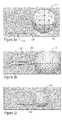
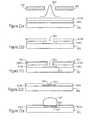
- FIGS. 1 a - cillustrate simulations of solder reflow according to embodiments of the present invention.
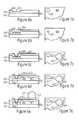
- FIGS. 2 a - g and 3 a - gare cross sectional and corresponding plan views illustrating operations of forming solder structures according to some embodiments of the present invention.
- FIGS. 4 a - h and 5 a - hare cross sectional and corresponding plan views illustrating operations of forming solder structures according to some other embodiments of the present invention.
- FIGS. 6 a - e and 7 a - eare cross sectional and corresponding plan views illustrating operations of forming solder structures according to still other embodiments of the present invention.
- FIGS. 8 a - d and 9 a - dare cross sectional and corresponding plan views illustrating operations of forming solder structures according to yet other embodiments of the present invention.
- FIGS. 10 a - e and 11 a - eare cross sectional and corresponding plan views illustrating operations of forming solder structures according to more embodiments of the present invention.
- FIGS. 12 a - h and 13 a - hare cross sectional and corresponding plan views illustrating operations of forming solder structures according to still more embodiments of the present invention.
- FIGS. 14 a - care cross sectional views illustrating stresses/strains on solder bumps resulting from differences in thermal expansion in electronic assemblies according to embodiments of the present invention.
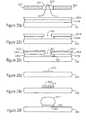
- FIGS. 15 a and 15 bare corresponding plan and cross sectional views illustrating a curved redistribution line (RDL) according to embodiments of the present invention.
- RDLredistribution line
- FIG. 15 cis a cross sectional view illustrating a floating RDL and solder bump according to embodiments of the present invention.
- FIGS. 16 a and 16 bare plan views illustrating expansion and contraction of a curved RDL according to embodiments of the present invention.
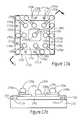
- FIG. 17 ais a plan view of a an integrated circuit device including RDLs and solder bumps according to embodiments of the present invention.
- FIG. 17 bis a cross sectional view taken along line I-I′ of FIG. 17 a according to embodiments of the present invention.
- FIGS. 18 a - dare cross sectional views illustrating steps of forming electrical and mechanical interconnections according to embodiments of the present invention.
- FIG. 19is a graph illustrating relationships between solder wetting down redistribution lines (RDLs) and resulting bump heights as functions of RDL line width with fixed bump pad diameters.
- RDLssolder wetting down redistribution lines
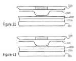
- FIGS. 20 a - f , 21 a - e , 22 , and 23are cross-sectional views illustrating methods of forming two layer lift-off patterns according to embodiments of the present invention.
- relative termssuch as beneath, upper, lower, top, and/or bottom may be used herein to describe one element's relationship to another element as illustrated in the figures. It will be understood that relative terms are intended to encompass different orientations of the device in addition to the orientation depicted in the figures. For example, if the device in one of the figures is turned over, elements described as below other elements would then be oriented above the other elements. The exemplary term below, can therefore, encompasses both an orientation of above and below.
- first and secondare used herein to describe various regions, layers and/or sections, these regions, layers and/or sections should not be limited by these terms. These terms are only used to distinguish one region, layer or section from another region, layer or section. Thus, a first region, layer or section discussed below could be termed a second region, layer or section, and similarly, a second region, layer or section could be termed a first region, layer or section without departing from the teachings of the present invention. Like numbers refer to like elements throughout.
- a Wafer Level Chip Scale Packagemay include a Redistribution Line (RDL) formed of Under Bump Metallurgy (UBM) that is not covered by dielectric so there is no solder dam.
- RDLRedistribution Line
- UBMUnder Bump Metallurgy
- solder flow down the RDLmay be reduced and/or prevented due to surface tension and the narrow line width of the RDL near the bump pad which may cause a pressure differential in the liquid solder between the pad and the RDL, and/or due to a contact angle between the solder and the RDL metal being greater on the line than the bump pad as a result of the presence of oxides on the metal surface of the RDL.
- the oxides on the bump padmay be chemically reduced by pattern-printed flux selectively printed on the bump pad, leaving oxide on the PDL line to reduce and/or prevent wetting of the solder down the RDL line.
- Bump height uniformitymay be maintained by adjusting the bump pad diameter to account for a volume of solder that may flow down the line.
- Redistribution wiring to a solder bump padhas been addressed according to a variety of methods.
- a propensity of solder to wet down a redistribution line (RDL)may result in loss of solder in the bump and possible collapse of the bump.
- RDLredistribution line
- a glass ‘solder dam’may be patterned across the RDL line to prevent and/or reduce a flow of solder from the bump pad down the RDL line.
- Use of a solder dammay control collapse of the bump (also referred to as the chip connection). This process may be referred to as a Controlled-Collapse Chip Connection or C4 process.
- Processes according to embodiments of the present inventionmay control a flow of solder (after solder ball/mass placement) using an internal pressure in the liquid solder that is caused by surface tension.
- the internal pressure (P)is related to the surface tension ( ⁇ ), by the inverse of the curvature of the surface:
- soldercan be confined to a bump pad without any material coatings on the bump pad.
- solder flow along the relatively narrow region of the RDL linecan be reduced and/or prevented by the decrease in the radius of curvature of the liquid solder.
- the resulting increase in pressuremay cause liquid solder on the narrow region of the RDL line to be drawn back into the solder bump on the bump pad (because the bump pad has a width greater than a width of the relatively narrow region of the bump pad).
- a preformed solder ball 101is placed on the solder bump pad 103 of a UBM (under bump metallurgy) coated RDL line 105 on the surface of an integrated circuit chip or other substrate. While preformed solder balls are discussed herein by way of example, any preformed solder mass may be used.
- FIG. 19is a graph illustrating relationships between solder wetting down redistribution lines (RDLs) and resulting bump heights as functions of RDL line width with fixed bump pad diameters and with fixed solder ball diameters before reflow.
- RDLssolder wetting down redistribution lines
- FIG. 19is provided for bump pads having a 245 ⁇ m (micrometer) diameter with RDL linewidths ranging from 20 ⁇ m (micrometer) to 241 ⁇ m (micrometer) in 13 ⁇ m (micrometer) increments.
- the wetted length of the RDLincreases with increasing linewidth (shown on the horizontal axis as a ratio of linewidth to bump pad diameter) for a fixed bump pad diameter when a solder ball (of fixed diameter) on the bump pad is subjected to reflow.
- the bump heightdecreases with increasing linewidth for a fixed bump pad diameter when a solder ball (of fixed diameter) on the bump pad is subjected to reflow due to increasing solder flow down the RDL.
- an electronic devicesuch as an integrated circuit semiconductor device
- a seed layer 207may be formed (for example, using sputtering) on the passivation layer 205 and on exposed portions of the wirebond pad 203 .
- the seed layer 207may include an adhesion layer (such as a layer of titanium-tungsten TiW) on the passivation layer 205 and a conduction layer (such as a layer of copper Cu) on the adhesion layer.
- the seed layer 207may include a layer of aluminum on the passivation layer 205 , and layer of nickel vanadium (Ni:V) on the aluminum layer, and a layer of copper on the nickel vanadium layer.
- a patterned photoresist layer 209(or other masking material) may be formed on the seed layer 207 , and the patterned photoresist layer 209 may expose portions seed layer 207 on which an RDL line and bump pad will be plated. Stated in other words, the patterned photoresist layer 209 may provide a plating template to plate an RDL line and bump pad. Moreover, the patterned photoresist layer 209 may be formed using photolithographic coat, expose, and develop operations.
- the RDL 211 and bump pad 213may be plated on portions of the seed layer 207 exposed through the photoresist layer 209 , and the photoresist layer 209 may be removed as shown in FIGS. 2 e and 3 e .
- the RDL 211 and bump pad 213may include a conduction layer (such as a layer of copper) on the seed layer 207 , a barrier layer (such as a layer nickel) on the conduction layer, and a conductive passivation layer (such as a layer of gold) on the barrier layer.
- a conduction layersuch as a layer of copper
- a barrier layersuch as a layer nickel
- a conductive passivation layersuch as a layer of gold
- an organic solderability preservativemay be provided as a passivation layer (instead of gold).
- the RDL passivation layermay be provided to protect against oxidation of the RDL 211 and bump pad 213 .
- the term RDLmay be defined to include both the relatively narrow RDL 211 and the relatively wide bump pad 213 .
- compositions of the RDL 211 and bump pad 213 other than those discussed abovemay be used.
- a conductive passivation layermay be omitted or a material other than gold may be provided as a conductive passivation layer.
- fluxcan be selectively applied to the bump pad 213 (without applying flux to the RDL 211 or portions thereof) before placing the preformed solder ball to reduce and/or prevent flow of solder down the RDL 211 during the reflow operation.
- a native oxide on the RDL 211may be maintained on the RDL 211 during the reflow operation, and a non-wetting characteristic of the native oxide may reduce and/or prevent flow of solder thereon.
- Fluxmay be selectively applied to the bump pad 213 , for example, using a flux stamp, printing, etc.
- soldermay be plated on the RDL 211 and the bump pad 213 before removing the patterned photoresist layer 209 , and the reflow operation may cause solder to flow from the RDL 211 to the bump pad 213 .
- a solder massmay be provided, for example, using a screen printed solder paste, using a printed solder, using a jetted solder, using evaporated solder, a plated solder, etc. A reflow operation may then be used provide a rounded solder bump and/or to flow solder from the RDL 211 to the bump pad 213 .
- an electronic devicesuch as an integrated circuit semiconductor device
- a substrate 401such as a semiconductor substrate
- a wirebond pad 403also referred to as an input/output pad
- an insulating passivation layer 405As shown in FIGS.
- a protective layer 406(such as a blanket layer of polyimide) may be deposited on the wirebond pad 403 and the passivation layer 405 , and the protective layer 406 may be patterned to expose portions of the wirebond pad 403 . While not shown in FIGS. 4 b and 5 b , the protective layer 406 may also be patterned to expose portions of dicing streets between integrated circuit devices on a manufacturing wafer.
- a seed layer 407may be formed (for example, using sputtering) on the protective layer 406 and on exposed portions of the wirebond pad 403 , as shown in FIGS. 4 c and 5 c .
- the seed layer 407may include an adhesion layer (such as a layer of titanium-tungsten TiW) on the protective layer 406 and a conduction layer (such as a layer of copper Cu) on the adhesion layer.
- the seed layer 407may include a layer of aluminum on the protective layer 406 , and layer of nickel vanadium (Ni:V) on the aluminum layer, and a layer of copper on the nickel vanadium layer.
- a patterned photoresist layer 409may be formed on the seed layer 407 , and the patterned photoresist layer 409 may expose portions of seed layer 407 on which an RDL line and bump pad will be plated. Stated in other words, the patterned photoresist layer 409 may provide a plating template to plate an RDL line and bump pad. Moreover, the patterned photoresist layer 409 may be formed using photolithographic coat, expose, and develop operations.
- the RDL 411 and bump pad 413may be plated on portions of the seed layer 407 exposed through the photoresist layer 409 , and the photoresist layer 409 may be removed as shown in FIGS. 4 f and 5 f .
- the RDL 411 and bump pad 413may include a conduction layer (such as a layer of copper) on the seed layer 407 , a barrier layer (such as a layer nickel) on the conduction layer, and a conductive passivation layer (such as a layer of gold) on the barrier layer.
- a conduction layersuch as a layer of copper
- a barrier layersuch as a layer nickel
- a conductive passivation layersuch as a layer of gold
- an organic solderability preservativemay be provided as a passivation layer (instead of gold).
- the RDL passivation layermay be provided to protect against oxidation of the RDL 411 and bump pad 413 .
- the term RDLmay be defined to include both the relatively narrow RDL 411 and the relatively wide bump pad 413 .
- compositions of the RDL 411 and bump pad 413 other than those discussed abovemay be used.
- a conductive passivation layermay be omitted or a material other than gold may be provided as a conductive passivation layer.
- Portions of the seed layer 407 not covered by the RDL 411 and/or the bump pad 413may be removed, for example, using a chemical etch, as shown in FIGS. 4 g and 5 g .
- a preformed solder ballmay then be placed on the bump pad 413 and subjected to a reflow operation to provide a solder bump 417 as shown in FIGS. 4 h and 5 h .
- a width of the RDL 411is sufficiently less than a width of the bump pad 413 , flow of solder down the RDL 411 during the reflow operation may be reduced and/or prevented. While preformed solder balls are discussed by way of example, any preformed solder mass may be used.
- fluxcan be selectively applied to the bump pad 413 (without applying flux to the RDL 411 or portions thereof) before placing the preformed solder ball to reduce and/or prevent flow of solder down the RDL 411 during the reflow operation.
- a native oxide on the RDL 411may be maintained on the RDL 411 during the reflow operation, and a non-wetting characteristic of the native oxide may reduce and/or prevent flow of solder thereon.
- Fluxmay be selectively applied to the bump pad 413 , for example, using a flux stamp, printing, etc.
- soldermay be plated on the RDL 411 and the bump pad 413 before removing the patterned photoresist layer 409 , and the reflow operation may cause solder to flow from the RDL 411 to the bump pad 413 .
- a solder massmay be provided, for example, using a screen printed solder paste, using a printed solder, using a jetted solder, using evaporated solder, a plated solder, etc.
- fluxmay be coated on an entire surface of the structure including the RDL 411 , the bump pad 413 , and the protective layer 406 before providing the solder bump 417 . A reflow operation may then be used provide a rounded solder bump and/or to flow solder from the RDL 411 to the bump pad 413 .
- the protective layer 406 of the process flow of FIGS. 4 a - h and 5 a - hmay be provided to protect the passivation layer 405 and/or the wirebond pad 403 from chemicals used in subsequent processing steps. While polyimide is discussed above by way of example, other materials such as silicones, elastomers, flexibilized epoxies, thermosetting polymers, fluoropolymers, and/or thermoplastic polymers may be used for the protective layer 406 . Other materials for protective layers are discussed, for example, in U.S. Pat. No. 6,211,572, the disclosure of which is hereby incorporated herein in its entirety by reference.
- the protective layer 406may extend onto dicing streets between integrated circuit device die of a wafer (including a plurality of integrated circuit device die) to “seal” the passivation layer 405 . More particularly, the passivation layer 405 may be removed from the dicing streets between the die so that the substrate 401 (or other material on the substrate) is exposed on the dicing streets between die before forming the protective layer 406 .
- the protective layer 406may extend onto portions of the dicing streets free of the passivation layer 405 surrounding each of the die without extending across the dicing streets. Central portions of the dicing streets through which the dicing saw will cut during subsequent dicing operations may be free of the protective layer 406 to reduce damage to the protective layer 406 when the wafer is diced to separate individual die. In other words, during a patterning step to expose portions of the wirebond pad 403 through the protective layer 406 , portions of the protective layer 406 on central portions of the dicing streets may be removed while maintaining portions of the protective layer 406 on edge portions of the dicing streets that are free of the passivation layer 405 . According to other embodiments of the present invention, the protective layer 406 may extend across the dicing streets between the die during dicing operations so that portions of the protective layer 406 in central portions of the dicing street are cut with the substrate 401 .
- a protective layer 606(such as a blanket layer of polyimide) may be deposited on the wirebond pad 603 and the passivation layer 605 , and the protective layer 606 may be patterned to expose portions of the wirebond pad 603 . While not shown in FIGS. 6 b and 7 b , the protective layer 606 may also be patterned to expose portions of dicing streets between integrated circuit devices on a manufacturing wafer.
- a seed layer 607may be selectively formed and/or patterned on the protective layer 606 and on exposed portions of the wirebond pad 603 , as shown in FIGS. 6 c and 7 c .
- the seed layer 607may include an adhesion layer (such as a layer of titanium-tungsten TiW) on the protective layer 606 and a conduction layer (such as a layer of copper Cu) on the adhesion layer.
- the seed layer 607may include a layer of aluminum on the protective layer 606 , and layer of nickel vanadium (Ni:V) on the aluminum layer, and a layer of copper on the nickel vanadium layer.
- the seed layer 607may include a titanium tungsten (TiW) layer on the protective layer 606 and a nickel layer (Ni) on the titanium tungsten layer.
- the seed layer 607may be formed by forming a continuous seed layer (for example, using sputtering) on the protective layer 606 , forming a photoresist mask on portions of the continuous seed layer corresponding to the RDL and bump pad, and removing portions of the seed layer exposed by the photoresist mask. The photoresist mask may then be stripped to provide the structure of FIGS. 6 c and 7 c.
- the seed layer 607may be formed by aligning a shadow mask over the protective layer 606 so that the shadow mask exposes portions of the protective layer 606 corresponding to the RDL and bump pad.
- the seed layermay then be deposited on the exposed portions of the protective layer 606 and on the shadow mask, for example, using evaporation, sputtering, and/or chemical vapor deposition.
- the shadow maskmay then be removed (together with portions of the seed layer thereon) to provide the structure of FIGS. 6 c and 7 c.
- the RDL 611 and bump pad 613may be plated on the seed layer 607 . More particularly, the RDL 611 and bump pad 613 may be plated using a catalytic/autocatalytic process and/or a substitutional process (such as an immersion process). For example, the RDL 611 and bump pad 613 may be plated using electroless-nickel/immersion-gold (ENIG).
- the RDL 611 and bump pad 613may include a conduction layer (such as a layer of copper) on the seed layer 607 , a barrier layer (such as a layer nickel) on the conduction layer, and a conductive passivation layer (such as a layer of gold) on the barrier layer.
- an organic solderability preservativemay be provided as a passivation layer (instead of gold).
- the RDL passivation layermay be provided to protect against oxidation of the RDL 611 and bump pad 613 .
- the term RDLmay be defined to include both the relatively narrow RDL 611 and the relatively wide bump pad 613 .
- compositions of the RDL 611 and bump pad 613 other than those discussed abovemay be used.
- a conductive passivation layermay be omitted or a material other than gold may be provided as a conductive passivation layer.
- a shadow maskmay be aligned over the protective layer 606 so that the shadow mask exposes portions of the protective layer 606 corresponding to the RDL and bump pad.
- Continuous layers of metal for the seed layer and for the RDL and bump padmay then be deposited on the exposed portions of the protective layer 606 and on the shadow mask, for example, using evaporation, sputtering, and/or chemical vapor deposition.
- the shadow maskmay then be removed (together with portions of the metal for the seed layer, RDL, and bump pad thereon) to provide the structure of FIGS. 6 d and 7 d.
- a preformed solder ballmay then be placed on the bump pad 613 and subjected to a reflow operation to provide a solder bump 617 as shown in FIGS. 6 e and 7 e .
- a width of the RDL 611is sufficiently less than a width of the bump pad 613 , flow of solder down the RDL 611 during the reflow operation may be reduced and/or prevented. While preformed solder balls are discussed by way of example, any preformed solder mass may be used.
- fluxcan be selectively applied to the bump pad 613 (without applying flux to the RDL 611 or portions thereof) before placing the preformed solder ball to reduce and/or prevent flow of solder down the RDL 611 during the reflow operation.
- a native oxide on the RDL 611may be maintained on the RDL 611 during the reflow operation, and a non-wetting characteristic of the native oxide may reduce and/or prevent flow of solder thereon.
- Fluxmay be selectively applied to the bump pad 613 , for example, using a flux stamp, printing, etc.
- soldermay be formed on the RDL 611 and on the bump pad 613 (for example by plating), and the reflow operation may cause solder to flow from the RDL 611 to the bump pad 613 .
- a solder massmay be provided, for example, using a screen printed solder paste, using a printed solder, using a jetted solder, using evaporated solder, a plated solder, etc. A reflow operation may then be used provide a rounded solder bump and/or to flow solder from the RDL 611 to the bump pad 613 .
- the protective layer 606 of the process flow of FIGS. 6 a - e and 7 a - emay be provided to protect the passivation layer 605 and/or the wirebond pad 603 from chemicals used in subsequent processing steps. While polyimide is discussed above by way of example, other materials such as silicones, elastomers, flexibilized epoxies, thermosetting polymers, fluoropolymers, and/or thermoplastic polymers may be used for the protective layer 606 . Other materials for protective layers are discussed, for example, in U.S. Pat. No. 6,211,572, the disclosure of which is hereby incorporated herein in its entirety by reference.
- the protective layer 606may extend onto dicing streets between integrated circuit device die of a wafer (including a plurality of integrated circuit device die) to “seal” the passivation layer 605 . More particularly, the passivation layer 605 may be removed from the dicing streets between the die so that the substrate 601 (or other material on the substrate) is exposed on the dicing streets between die before forming the protective layer 606 .
- the protective layer 606may extend onto portions of the dicing streets free of the passivation layer 605 surrounding each of the die without extending across the dicing streets. Central portions of the dicing streets through which the dicing saw will cut during subsequent dicing operations may be free of the protective layer 606 to reduce damage to the protective layer 606 when the wafer is diced to separate individual die. In other words, during a patterning step to expose portions of the wirebond pad 603 through the protective layer 606 , portions of the protective layer 606 on central portions of the dicing streets may be removed while maintaining portions of the protective layer 606 on edge portions of the dicing streets that are free of the passivation layer 605 . According to other embodiments of the present invention, the protective layer 606 may extend across the dicing streets between the die during dicing operations so that portions of the protective layer 606 in central portions of the dicing street are cut with the substrate 601 .
- an electronic devicesuch as an integrated circuit semiconductor device
- a substrate 801such as a semiconductor substrate
- a wirebond pad 803also referred to as an input/output pad
- an insulating passivation layer 805As shown in FIGS. 8 a and 9 a , an electronic device (such as an integrated circuit semiconductor device) may include a substrate 801 (such as a semiconductor substrate), a wirebond pad 803 (also referred to as an input/output pad), and an insulating passivation layer 805 .
- a protective layer 806(such as a blanket layer of polyimide) may be deposited on the wirebond pad 803 and the passivation layer 805 , and the protective layer 806 may be patterned to expose portions of the wirebond pad 803 . While not shown in FIGS. 8 b and 9 b , the protective layer 806 may also be patterned to expose portions of dicing streets between integrated circuit devices on a manufacturing wafer.
- a shadow mask 809may be aligned over the protective layer 806 so that the shadow mask exposes portions of the protective layer 806 corresponding to the RDL and bump pad.
- layers of metal for the RDL and bump padmay then be deposited on the exposed portions of the protective layer 806 and on the shadow mask 809 , for example, using evaporation, sputtering, and/or chemical vapor deposition. More particularly, portions of the metal layers on the protective layer 806 may define the RDL 811 and the bump pad 813 , and excess metal 812 may be formed on the shadow mask 809 .
- the metal for the RDL 811 and bump pad 813may include a seed/adhesion layer on the protective layer 806 , a conduction layer (such as a layer of copper) on the seed/adhesion layer, a barrier layer (such as a layer of nickel) on the seed/adhesion layer, and a passivation layer (such as a layer of gold or an organic solderability preservative) on the barrier layer.
- the seed/adhesion layermay include a titanium-tungsten (TiW) layer on the protective layer 806 and a copper (Cu) layer on the titanium-tungsten layer.
- the seed/adhesion layer 807may include a layer of aluminum on the protective layer 806 , and layer of nickel vanadium (Ni:V) on the aluminum layer, and a layer of copper on the nickel vanadium layer.
- the seed/adhesion layermay include a titanium tungsten (TiW) layer on the protective layer 806 and a nickel layer (Ni) on the titanium-tungsten layer.
- TiWtitanium tungsten
- Ninickel layer
- compositions of the RDL 811 and bump pad 813 other than those discussed abovemay be used.
- a conductive passivation layermay be omitted or a material other than gold may be provided as a conductive passivation layer.
- Fluxcan be selectively provided on the bump pad 813 , and a preformed solder ball 816 may then be placed on the bump pad 813 (including the flux thereon) while maintaining the shadow mask 809 and the excess metal 812 thereon as shown in FIGS. 8 c and 9 c .
- the shadow mask 809may thus provide a stencil for placement of the solder ball 816 because the portion of the opening in the shadow mask 809 over the bump pad 813 is significantly wider than the portion of the opening over the RDL 811 .
- a preformed solder ball 813 with a diameter greater than a width of the RDLmay thus fall selectively into the portion of the opening in the solder mask 809 exposing the bump pad 813 .
- a single mask alignment(for the shadow mask 809 ) may be used both for RDL 811 and bump pad 813 patterning and for solder ball 816 placement. While a preformed solder ball is discussed by way of example, any preformed solder mass having a dimension greater than a width of the relatively narrow RDL may be used.
- the solder ball 816can be subjected to a reflow operation while maintaining the shadow mask 809 and the excess metal 812 thereon, and the shadow mask 809 and the excess metal 812 can then be removed to provide the solder bump 817 of FIGS. 8 d and 9 d .
- By selectively applying flux to the bump pad 813 (without applying flux to the RDL 811 or to the excess metal 812 or portions thereof) before placing the preformed solder ball 816flow of solder onto the RDL 811 and/or the excess metal 812 can be reduced and/or eliminated during the reflow operation.
- a native oxide on the RDL 811 and excess metal 812may be maintained during the reflow operation, and a non-wetting characteristic of the native oxide may reduce and/or prevent flow of solder thereon.
- Fluxmay be selectively applied to the bump pad 813 , for example, using a flux stamp, printing, etc.
- the shadow mask 809 and the excess metal 812 thereonmay be removed before performing the reflow operation, and a difference in widths of the bump pad 813 and the RDL 811 may be sufficient to reduce flow of solder down the RDL 811 .
- a solder massmay be provided, for example, using a screen printed solder paste, using a printed solder, using a jetted solder, using evaporated solder, a plated solder, etc.
- a reflow operationmay then be used provide a rounded solder bump and/or to flow solder from the RDL 811 to the bump pad 813 .
- the protective layer 806 of the process flow of FIGS. 8 a - d and 9 a - dmay be provided to protect the passivation layer 805 and/or the wirebond pad 803 from chemicals used in subsequent processing steps. While polyimide is discussed above by way of example, other materials such as silicones, elastomers, flexibilized epoxies, thermosetting polymers, fluoropolymers, and/or thermoplastic polymers may be used for the protective layer 806 . Other materials for protective layers are discussed, for example, in U.S. Pat. No. 6,211,572, the disclosure of which is hereby incorporated herein in its entirety by reference.
- the protective layer 806may extend onto dicing streets between integrated circuit device die of a wafer (including a plurality of integrated circuit device die) to “seal” the passivation layer 805 . More particularly, the passivation layer 805 may be removed from the dicing streets between the die so that the substrate 801 (or other material on the substrate) is exposed on the dicing streets between die before forming the protective layer 806 .
- the protective layer 806may extend onto portions of the dicing streets free of the passivation layer 805 surrounding each of the die without extending across the dicing streets. Central portions of the dicing streets through which the dicing saw will cut during subsequent dicing operations may be free of the protective layer 806 to reduce damage to the protective layer 806 when the wafer is diced to separate individual die. In other words, during a patterning step to expose portions of the wirebond pad 803 through the protective layer 806 , portions of the protective layer 806 on central portions of the dicing streets may be removed while maintaining portions of the protective layer 806 on edge portions of the dicing streets that are free of the passivation layer 805 . According to other embodiments of the present invention, the protective layer 806 may extend across the dicing streets between the die during dicing operations so that portions of the protective layer 806 in central portions of the dicing street are cut with the substrate 801 .
- an electronic devicesuch as an integrated circuit semiconductor device
- a substrate 1001such as a semiconductor substrate
- a wirebond pad 1003also referred to as an input/output pad
- an insulating passivation layer 1005As shown in FIGS.
- a protective layer 1006(such as a blanket layer of polyimide) may be deposited on the wirebond pad 1003 and the passivation layer 1005 , and the protective layer 1006 may be patterned to expose portions of the wirebond pad 1003 . While not shown in FIGS. 10 b and 11 b , the protective layer 1006 may also be patterned to expose portions of dicing streets between integrated circuit devices on a manufacturing wafer.
- a shadow mask 1009 a - bmay be aligned over the protective layer 1006 so that the shadow mask exposes portions of the protective layer 1006 corresponding to the RDL and bump pad.
- layers of metal for the RDL and bump padmay then be deposited on the exposed portions of the protective layer 1006 and on the shadow mask 1009 a - b , for example, using evaporation, sputtering, and/or chemical vapor deposition. More particularly, portions of the metal layers on the protective layer 1006 may define the RDL 1011 and the bump pad 1013 , and excess metal 1012 may be formed on the shadow mask 1009 a - b.
- the shadow maskmay include first shadow mask layer 1009 a and second shadow mask layer 1009 b , and the two shadow mask layers may have different compositions (e.g., comprise different materials and/or concentrations thereof).
- the two shadow mask layersmay have different concentrations of a chemical amplifier to provide different sensitivities to light. Chemical amplifiers are discussed, for example, in U.S. Pat. No. 5,595,855, the disclosure of which is hereby incorporated herein in its entirety by reference.
- the two shadow mask layersmay develop at different rates and/or the two shadow mask layers may be selectively stripped using different solutions.
- the second shadow mask 1009 bmay be removed while maintaining the first shadow mask layer 1009 a .
- first shadow mask layer 1009 ais more photosensitive than the second shadow mask layer 1009 b
- undercutting of the first shadow mask layer 1009 a relative to the second shadow mask layer 1009 bmay facilitate subsequent stripping of the second shadow mask layer. While not shown in FIG. 10 b , portions of the excess metal 1012 may extend on vertical edges of the second shadow mask layer 1009 b.
- Each of the shadow mask layers 1009 a - bmay be applied by spin coating and/or as a laminate sheet. According to some embodiments of the present invention, solid films of the two different shadow mask layers 1009 a - b may be provided together as a laminated sheet that is then applied to the protective layer 1006 . Once applied to the protective layer 1006 , the shadow mask layers 1009 a - b may be patterned using photolithographic exposure and develop steps.
- the metal for the RDL 1011 and bump pad 1013may include a seed/adhesion layer on the protective layer 1006 , a conduction layer (such as a layer of copper) on the seed/adhesion layer, a barrier layer (such as a layer of nickel) on the seed/adhesion layer, and a passivation layer (such as a layer of gold or an organic solderability preservative) on the barrier layer.
- the seed/adhesion layermay include a titanium-tungsten (TiW) layer on the protective layer 1006 and a copper (Cu) layer on the titanium-tungsten layer.
- the seed/adhesion layer 1007may include a layer of aluminum on the protective layer 1006 , layer of nickel vanadium (Ni:V) on the aluminum layer, and a layer of copper on the nickel vanadium layer.
- the seed/adhesion layermay include a titanium tungsten (TiW) layer on the protective layer 1006 and a nickel layer (Ni) on the titanium-tungsten layer.
- TiWtitanium tungsten
- Ninickel layer
- compositions of the RDL 1011 and bump pad 1013 other than those discussed abovemay be used.
- a conductive passivation layermay be omitted or a material other than gold may be provided as a conductive passivation layer.
- the second shadow mask layer 1009 b and the excess metal 1012 thereonmay be selectively removed/stripped while maintaining the first shadow mask layer 1009 a on the protective layer 1006 .
- Stripping of the second shadow mask layer 1009 bmay be facilitated by providing that the first shadow mask layer 1009 a is undercut relative to the second shadow mask layer 1009 b so that exposure of the second shadow mask layer 1009 b to a stripping solution is increased.
- a preformed solder ball 1016may then be placed on the bump pad 1013 while maintaining the first shadow mask layer 1009 a as shown in FIGS. 10 d and 11 d .
- the first shadow mask layer 1009 amay thus provide a stencil for placement of the solder ball 1016 because the portion of the opening in the first shadow mask layer 1009 a over the bump pad 1013 is significantly wider than the portion of the opening over the RDL 1011 .
- a solder ball 1016 with a diameter greater than a width of the RDLmay thus fall selectively into the portion of the opening in the first shadow mask layer 1009 a exposing the bump pad 1013 .
- a single mask alignment(for the shadow mask 1009 a - b ) may be used both for RDL 1011 and bump pad 1013 patterning and for solder ball 1016 placement.
- RDLmay be defined to include both the relatively narrow RDL 1011 and the relatively wide bump pad 1013 . While a preformed solder ball is discussed by way of example, any preformed solder mass having a dimension greater than a width of the relatively narrow RDL may be used.
- the solder ball 1016can be subjected to a reflow operation while maintaining the first shadow mask layer 1009 a , and the first shadow mask layer 1009 a can then be removed to provide the solder bump 1017 of FIGS. 10 e and 11 e .
- the first shadow mask layer 1009 amay be maintained after reflowing the solder ball 1016 .
- a difference in widths of the bump pad 1013 and the RDL 1011may be sufficient to reduce flow of solder down the RDL 1011 .
- fluxmay be selectively applied to the bump pad 1013 (without applying flux to the RDL 1011 or portions thereof) before placing the preformed solder ball 1016 , to further reduce and/or eliminate flow of solder onto the RDL 1011 .
- a native oxide on the RDL 1011may be maintained during the reflow operation, and a non-wetting characteristic of the native oxide may reduce and/or prevent flow of solder thereon.
- Fluxmay be selectively applied to the bump pad 1013 , for example, using a flux stamp, printing, etc.
- a solder massmay be provided, for example, using a screen printed solder paste, using a printed solder, using a jetted solder, using evaporated solder, a plated solder, etc.
- a reflow operationmay then be used provide a rounded solder bump and/or to flow solder from the RDL 1011 to the bump pad 1013 .
- the protective layer 1006 of the process flow of FIGS. 10 a - e and 11 a - emay be provided to protect the passivation layer 1005 and/or the wirebond pad 1003 from chemicals used in subsequent processing steps. While polyimide is discussed above by way of example, other materials such as silicones, elastomers, flexibilized epoxies, thermosetting polymers, fluoropolymers, and/or thermoplastic polymers may be used for the protective layer 1006 . Other materials for protective layers are discussed, for example, in U.S. Pat. No. 6,211,572, the disclosure of which is hereby incorporated herein in its entirety by reference.
- the protective layer 1006may extend onto dicing streets between integrated circuit device die of a wafer (including a plurality of integrated circuit device die) to “seal” the passivation layer 1005 . More particularly, the passivation layer 1005 may be removed from the dicing streets between the die so that the substrate 1001 (or other material on the substrate) is exposed on the dicing streets between die before forming the protective layer 1006 .
- the protective layer 1006may extend onto portions of the dicing streets free of the passivation layer 1005 surrounding each of the die without extending across the dicing streets. Central portions of the dicing streets through which the dicing saw will cut during subsequent dicing operations may be free of the protective layer 1006 to reduce damage to the protective layer 1006 when the wafer is diced to separate individual die. In other words, during a patterning step to expose portions of the wirebond pad 1003 through the protective layer 1006 , portions of the protective layer 1006 on central portions of the dicing streets may be removed while maintaining portions of the protective layer 1006 on edge portions of the dicing streets that are free of the passivation layer 1005 . According to other embodiments of the present invention, the protective layer 1006 may extend across the dicing streets between the die during dicing operations so that portions of the protective layer 1006 in central portions of the dicing street are cut with the substrate 1001 .
- an electronic devicesuch as an integrated circuit semiconductor device
- a substrate 1201such as a semiconductor substrate
- a wirebond pad 1203also referred to as an input/output pad
- an insulating passivation layer 1205As shown in FIGS. 12 a and 13 a , an electronic device may include a substrate 1201 (such as a semiconductor substrate), a wirebond pad 1203 (also referred to as an input/output pad), and an insulating passivation layer 1205 .
- a compliant dielectric layer 1204(such as a polymer dielectric layer) may be selectively formed on portions of the insulating passivation layer 1205 , for example, using screen printing and/or liquid jetting, so that a photolithographic patterning operation is not required. If the compliant dielectric layer 1204 is not used to protect the wirebond pad 1203 as a solder mask or dam, the compliant dielectric layer 1204 may be deposited only where it is to be used to provide compliance (e.g., where a solder bump will be formed).
- the compliant dielectric layer 1204may be a layer of silicone rubber (such as a room temperature vulcanizing (RTV) silicone rubber) formed by stencil printing. A mound of silicone rubber may be deposited at a site for a subsequently formed solder bump. If the compliant dielectric layer 1204 is not used to cover and expose different portions of the wirebond pad 1203 , fine feature printing of the compliant dielectric layer 1204 may not be required. Moreover, the compliant dielectric layer 1204 may be printed onto a central portion of the die to avoid an outer ring of wirebond pads.
- RTVroom temperature vulcanizing
- a seed layer 1207may be formed (for example, using sputtering) on the passivation layer 1205 , on exposed portions of the wirebond pad 1203 , and on the compliant dielectric layer 1204 .
- the seed layer 1207may include an adhesion layer (such as a layer of titanium-tungsten TiW) on the passivation layer 1205 and on the compliant dielectric layer 1204 and a conduction layer (such as a layer of copper Cu) on the adhesion layer.
- the seed layer 1207may include a layer of aluminum on the passivation layer 1205 and on the compliant dielectric layer 1204 , and layer of nickel vanadium (Ni:V) on the aluminum layer, and a layer of copper on the nickel vanadium layer.
- Ni:Vnickel vanadium
- a patterned photoresist layer 1209may be formed on the seed layer 1207 , and the patterned photoresist layer 1209 may expose portions seed layer 1207 on which an RDL line and bump pad will be plated. Stated in other words, the patterned photoresist layer 1209 may provide a plating template to plate an RDL line and bump pad. Moreover, the patterned photoresist layer 1209 may be formed using photolithographic coat, expose, and develop operations.
- the RDL 1211 and bump pad 1213may be plated on portions of the seed layer 1207 exposed through the photoresist layer 1209 , and the photoresist layer 1209 may be removed as shown in FIGS. 12 f and 13 f .
- the RDL 1211 and bump pad 1213may include a conduction layer (such as a layer of copper) on the seed layer 1207 , a barrier layer (such as a layer nickel) on the conduction layer, and a conductive passivation layer (such as a layer of gold) on the barrier layer.
- a conduction layersuch as a layer of copper
- a barrier layersuch as a layer nickel
- a conductive passivation layersuch as a layer of gold
- an organic solderability preservativemay be provided as a passivation layer (instead of gold).
- the PDL passivation layermay be provided to protect against oxidation of the RDL 1211 and bump pad 1213 .
- the term RDLmay be defined to include both the relatively narrow RDL 1211 and the relatively wide bump pad 1213 .
- compositions of the RDL 1211 and bump pad 1213 other than those discussed abovemay be used.
- a conductive passivation layermay be omitted or a material other than gold may be provided as a conductive passivation layer.
- Portions of the seed layer 1207 not covered by the RDL 1211 and/or the bump pad 1213may be removed, for example, using a chemical etch, as shown in FIGS. 12 g and 13 g .
- a preformed solder ballmay then be placed on the bump pad 1213 and subjected to a reflow operation to provide a solder bump 1217 as shown in FIGS. 12 h and 13 h .
- a width of the RDL 1211is sufficiently less than a width of the bump pad 1213 , flow of solder down the RDL 1211 during the reflow operation may be reduced and/or prevented. While preformed solder balls are discussed by way of example, any preformed solder mass may be used.
- fluxcan be selectively applied to the bump pad 1213 (without applying flux to the RDL 1211 or portions thereof) before placing the preformed solder ball to reduce and/or prevent flow of solder down the RDL 1211 during the reflow operation.
- a native oxide on the RDL 1211may be maintained on the RDL 1211 during the reflow operation, and a non-wetting characteristic of the native oxide may reduce and/or prevent flow of solder thereon.
- Fluxmay be selectively applied to the bump pad 1213 , for example, using a flux stamp, printing, etc.
- soldermay be plated on the RDL 1211 and the bump pad 1213 before removing the patterned photoresist layer 1209 , and the reflow operation may cause solder to flow from the RDL 1211 to the bump pad 1213 .
- a solder massmay be provided, for example, using a screen printed solder paste, using a printed solder, using a jetted solder, using evaporated solder, a plated solder, etc. A reflow operation may then be used provide a rounded solder bump and/or to flow solder from the RDL 1211 to the bump pad 1213 .
- the seed layer 1207 , RDL 1211 and bump pad 1213may be formed on the wirebond pad 1203 , insulating passivation layer 1205 , and compliant dielectric layer 1204 using steps similar to those discussed above with respect to FIGS. 2 b - 2 g and 3 b - 3 g .
- the seed layer 1207 , RDL 1211 and bump pad 1213may be formed using steps similar to those discussed above with respect to FIGS. 4 c - h and 5 c - h , FIGS. 6 b - e and 7 b - e , FIGS.
- a protective layer(as discussed above with respect to FIGS. 4 b and 5 b , FIGS. 6 b and 7 b , FIGS. 8 b and 9 b , FIGS. 10 b and 11 b ) may also be provided between the compliant dielectric layer 1204 and the insulating passivation layer 1205 . Such a protective layer may also be provided between portions of the wirebond pad 1203 and the seed layer 1207 .
- the compliant dielectric layer 1204By forming the compliant dielectric layer 1204 , the RDL 1211 , the bump pad 1213 , and the solder bump 1217 as discussed above with respect to FIGS. 12 a - h and 13 a - h , a number of photolithography steps may be reduced as compared to a conventional 4-mask Redistribution Line (RDL) Chip Scale Package (CSP).
- the RDL 1211 and bump pad 1213may be capped with a UBM (e.g., Ni and/or Au) to protect the conductor layer (e.g., Cu) of the RDL 1211 and bump pad 1213 by providing protection from moisture and/or corrosive agents in the environment.
- the conductor layer (e.g., Cu) of the RDL 1211 and bump pad 1213may be left bare if the system package provides adequate protection, and UBM is not otherwise required.
- the RDL 1211is sufficiently narrower than the bump pad 1213 , and/or by selectively providing flux on the bump pad 1213 (and not on the RDL 1211 or portions thereof) flow of solder onto the RDL 1211 may be reduced and/or prevented. Accordingly, the RDL 1211 and/or UBM on the RDL 1211 may be completely exposed and not covered by a dielectric.
- solder bump 1217is laterally spaced apart from the via in the insulating passivation layer 1205 exposing portions of the wirebond pad 1203 (so that the wirebond pad 1203 is not under the solder bump 1217 )
- the solder bumpmay rest on a relatively flat bump pad 1213 thereby improving stress/strain distribution.
- the RDL line 1211may also define a passive electrical element such as a resistor, a planar inductor coil, and/or one or more plates of a capacitor.
- solder bumpsmay be provided on the compliant dielectric layer 1204 while other solder bumps are provided on portions of the insulating passivation layer 1205 without the compliant dielectric layer 1204 . More particularly, solder bumps closer to an edge of the substrate 1201 may be provided on the compliant dielectric layer because these solder bumps may be subjected to greater stress/strain and the compliant dielectric layer may absorb some of this stress/strain. Solder bumps closer to a center of the substrate 1201 may be provided without the compliant dielectric layer because these solder bumps may be subjected to less stress/strain. Moreover, solder bumps without the compliant dielectric layer may provide a more rigid attachment to another substrate (such as a printed circuit board).
- a protective polyimide layer(shown as protective layers 406 , 606 , 806 , 1006 in FIGS. 4 b , 5 b , 6 b , 7 b , 8 b , 9 b , 10 b , and 11 b ) may be omitted (as shown in FIGS. 2 a - g and 3 a - g and FIGS. 12 a - h and 13 a - h ).
- a TiW barrier layer of the seed layer 1207can be etched with chemicals that are relatively gentle with respect to an aluminum wirebond pad 1203 and with respect to a glass passivation layer 1205 , so that the aluminum wirebond pad 1203 (or portions thereof) and the glass passivation layer 1205 (or portions thereof) can be exposed during the final etch and so that a polyimide layer is not required to reduce a size of an exposed portion of the wirebond pad 1203 .
- solder flow on the RDL 1211can be reduced and/or prevented by providing a difference in width between a portion of the RDL 1211 contacting the bump pad 1213 and/or by selectively providing flux on the bump pad 1213 , a size of a capture pad portion of the RDL 1211 covering the aluminum wirebond pad 1203 may not need to be small (to provide solder pressure control) and can be any convenient size. Accordingly, the RDL 1211 may include a relatively large capture pad portion that completely seals the aluminum wirebond pad 1203 .
- a conduction layer (e.g., copper) of the RDL 1211 and bump pad 1213can be made relatively thick, for example, greater than about 0.5 ⁇ m (micrometers) to improve current distribution under the bump.
- Relatively thick conduction layersare discussed, for example, in U.S. Pat. No. 6,960,828 and in U.S. patent application Ser. No. 11/270,366, the disclosures of which are hereby incorporated herein in their entirety by reference.
- multiple relatively narrow RDL linesmay be connected to a pad to reduce resistance and/or increase current carrying capacity.
- FIGS. 2 a - g and 3 a - gIn the process flows illustrated in FIGS. 2 a - g and 3 a - g , in FIGS. 4 a - h and 5 a - h , in FIGS. 6 a - h and 7 a - h , in FIGS. 8 a - d and 9 a - d, in FIGS. 10 a - 10 e and 11 a - 11 e , or in FIGS.
- operations of forming the solder bumps 217 , 417 , 617 , 817 , 1017 , or 1217may be performed by placing a solid preformed solder mass (e.g., a solder or sphere) on the bump pad ( 213 , 413 , 613 , 813 , 1013 , or 1213 ).
- a solid preformed solder masse.g., a solder or sphere
- placing the solid preformed solder massmay be preceded by selectively providing flux on the bump pad ( 213 , 413 , 613 , 813 , 1013 , or 1213 ) while maintaining exposed portions of the RDL line ( 211 , 411 , 611 , 811 , 1011 , or 1211 ) free of the flux.
- an oxide of the metal on the bump pad ( 213 , 413 , 613 , 813 , 1013 , or 1213 )may thus be chemically reduced while the oxide of the metal on portions of the RDL line ( 211 , 411 , 611 , 811 , 1011 , or 1211 ) may be maintained.
- wetting of the solder to the bump pad ( 213 , 413 , 613 , 813 , 1013 , or 1213 )can be enhanced while wetting of the solder to the RDL line ( 211 , 411 , 611 , 811 , 1011 , or 1211 ) during reflow can be reduced so that the solder is maintained on the bump pad without requiring formation and/or patterning of a layer or dam on the RDL line.
- the oxide of the RDL metalmay occur as a result of exposure of the RDL metal to oxygen in the atmosphere.
- portions of the RDL 1211 and bump pad 1213may shear free from the compliant dielectric layer 1204 allowing the solder bump 1217 , the bump pad 1213 , and portions of the RDL 1211 to ‘float’ relative to the substrate 1201 (also referred to as a die).
- Adhesion of metal of the RDL 1211 to the wirebond pad 1203may be greater than the resulting applied force and the RDL 1211 may provide compliance along its length (for example by providing a curve along a length of the RDL 1211 ) to absorb a stress/strain of motion of the solder bump 1217 (at an end of the RDL 1211 ) relative to the substrate 1201 .
- Cantilevered RDL stress/strain relief structuresare discussed in greater detail below.
- An RDL that adheres poorly to a final dielectric layer on which it is formedcan be made to detach from the dielectric layer under conditions of high stress/strain (for example, due to differences in thermal expansion of two substrates between which a solder bump is attached).
- the detached RDLmay then be allowed to ‘float’, so that stress/strain on a solder bump at a floating end of the RDL may be reduced.
- the RDL linemay be attached to the die at one end only at the via to the wirebond pad, such that the bump is on a cantilevered arm that allows small displacements with reduced stress/strain on the solder bump. Stress/strain may be absorbed by the RDL which distributes the stress/strain over a much longer distance.
- solder bumps on a die at a relatively small distance from a neutral point of stress/strainmay provide a rigid mechanical connection between the die and another substrate, while solder bumps on the die at a relatively large distance from the neutral point of stress/strain may be flexibly coupled to the die through a “floating” RDL to reduce stress/strain.
- a cyclic thermal fatigue lifetime of a flip chip solder jointmay depend on the distance-to-neutral point (DNP) raised to an exponent of nearly two.
- DNPdistance-to-neutral point
- the DNP for each solder bump on the diemay need to be less than some critical value. Where it is desired to place a solder bump at a DNP larger than the critical value, reduction and/or elimination of stress/strain for these high DNP bumps may be needed.
- a semiconductor integrated circuit (IC) device 1401may be electrically and mechanically coupled to a substrate 1405 (such as a printed circuit board) using a plurality of solder bumps 1403 a - e .
- a substrate 1405such as a printed circuit board
- bump pads of the IC device 1401 and the substrate 1405may be substantially aligned so that lateral stresses/strains on the solder bumps 1403 a - e may be relatively small as shown in FIG. 14 a .
- the substrate 1405may expand relative to the IC device 1401 as shown in FIG. 14 b .
- the substrate 1405may contract relative to the IC device 1401 as shown in FIG. 14 c .
- the central solder bump 1403 c(located at the neutral point of thermal expansion) is thus subject to relatively little lateral stress/strain as the assembly is heated and/or cooled.
- Other solder bumps with greater distances to the neutral point of thermal expansionmay be subjected lateral stresses/strains as the assembly is heated and cooled.
- the outer solder bumps 1403 a and 1403 emay be subjected to greater lateral stresses/strains than intermediate solder bumps 1403 b and 1403 d.
- Some metalsdo not adhere well to some polymer dielectrics unless the polymer dielectric is pretreated, for example, using a plasma roughening. If the pretreatment is reduced and/or eliminated, low adhesion between an RDL and the underlying polymer dielectric may result. According to some embodiments of the present invention shown in FIGS.
- an RDL 1501 for a high DNP bump 1505 on IC device substrate 1502may be formed on a final passivation layer 1503 (such as a polymer dielectric layer) with adhesion sufficient to provide robustness during processing, testing, handling, and assembly, yet with adhesion low enough to allow release after coupling to another substrate (such as a printed circuit board) under stress/strain in the assembly due to differences of thermal expansion. If the RDL 1501 is not self-passivating, protection may be provided using a suitable coating such as electroless gold.
- a difference of expansivity between the IC device substrate 1502 and the other substrate (such as a printed circuit board) to which the high DNP bump 1505 is attachedmay cause lateral stresses/strains to be applied to the solder bump 1505 and the metal RDL 1501 that exceed an adhesive strength of an interface between the final passivation layer 1503 and the RDL 1501 so that the RDL 1501 separates from the final passivation layer 1503 .
- Excessive stress/strain to these “floating” linesmay be reduced by providing that the IC device is firmly held to the other substrate by other relatively low-DNP solder bumps.
- a total strain at 125 degrees C.can exceed 2.25% for corner solder bumps.
- a critical elastic strain limit for high lead soldermay be about 0.02% so that the corner bumps may be well into a plastic strain region. Because fatigue life decreases as the square of plastic strain, a significant improvement in reliability may be provided if highest DNP bumps are provided with stress/strain relief. If strain on bumps outside a 3.5 mm radius from the neutral point is relieved, thermal cycle fatigue life may increase on the order of 100%. In this example based on a circular array geometry, 96% of the bumps may be provided with standard vias and RDL lines and 4% may be provide with “floating” RDL lines to reduce stress/strain.
- the curved RDL 1501may stretch and/or compress to accommodate lateral displacements of the substrate to which the integrated circuit device substrate 1502 is attached as shown in FIGS. 16 a - b.
- solder bumps most distant from a neutral point of thermal expansion of an IC device substratemay be provided on a compliant dielectric layer while solder bumps closest to the neutral point of thermal expansion may be provided on a relatively rigid dielectric layer.
- the solder bumps on the relatively rigid dielectric layermay thus provide a relatively rigid coupling between the IC device substrate and another substrate (such as a printed circuit board), while the compliant dielectric layer may reduce lateral stress/strain on the solder bumps most distant form the neutral point of thermal expansion.
- a compliant dielectric layer 1701may be provided between some of the solder bumps (e.g., solder bumps 1705 a - h ) and the insulating passivation layer 1703 but not others (e.g., solder bump 1705 i). More particularly, wirebond pads 1711 may be provided around a periphery of the integrated circuit device substrate 1707 , and holes in the insulating passivation layer 1703 may expose portions of the wirebond pads 1711 .
- RDLs 1709 a - imay provide electrical coupling between respective wirebond pads 1711 a - i and solder bumps 1705 a - i .
- other unused wirebond pads 1711 j - pmay be exposed through vias in the insulating passivation layer 1703 .
- the term RDLmay be defined to include bump pads (i.e., widened portions of the RDL) on which the respective solder bumps will be provided and/or to include capture pads on the respective wirebond pads.
- the insulating passivation layer 1703 and the compliant dielectric layer 1701may comprise different materials, and the insulating passivation layer 1703 may be more rigid than the compliant dielectric layer 1701 .
- adhesion between the insulating passivation layer 1703 and the RDLs 1709 a - imay be greater than adhesion between compliant dielectric layer 1701 and the RDLs 1709 a - i .
- the peripheral solder bumps 1705 a - h and associated RDLs 1709 a - hmay float as discussed above with respect to FIG. 15 c to reduce stress/strain resulting from thermal expansion, while the central solder bump 1705 i and RDL 1709 i may remain secured to the insulating passivation layer 1703 .
- solder bump 1705 iWhile only one solder bump 1705 i is shown on the central portion of the insulating passivation layer 1703 that is free of the compliant dielectric layer 1701 , a plurality of solder bumps could be provided on the central portion of the insulating passivation layer 1703 .
- the central solder bump(s)may support connection of the IC substrate 1707 to another substrate (such as a printed circuit board) in an electronic assembly against forces resulting, for example, from dropping, bending, shearing, and/or impact. Accordingly, reliability of the electronic assembly may be increased.
- the RDLs 1709 a - i and solder bumps 1705 a - imay be formed as discussed above with respect to FIGS. 2 a - g and 3 a - g , FIGS. 4 a - h and 5 a - h , FIGS. 6 a - e and 7 a - e , FIGS. 8 a - d and 9 a - d , FIGS. 10 a - e and 11 a - e, and/or FIGS. 12 a - h and 13 a - h .
- the compliant dielectric layer 1701may be formed as discussed above with respect to FIGS.
- the compliant dielectric layer 1701may be a layer including a silicone, an elastomer, a polyimide, a flexibilized epoxy, a thermosetting polymer, a fluoropolymer, and/or a thermoplastic polymer, and/or other compliant material, and the compliant dielectric layer 1701 may be selectively formed and/or printed (for example, using stencil printing, needle dispense, pad printing, etc.) so that a separate photolithographic masking step is not required and so that cost may be reduced.
- the insulating passivation layer 1703may include a layer of an inorganic material such as silicon oxide, silicon nitride, and/or silicon oxynitride, or the insulating layer may be a layer of polyimide. If a polyimide layer is used as the insulating passivation layer 1703 , the insulating passivation layer 1703 may be subjected to a surface treatment (such as a roughening) to promote adhesion between the RDLs and the insulating passivation layer 1703 , while a surface of the compliant dielectric layer 1701 may remain untreated to reduce adhesion between the RDLs and the compliant dielectric layer 1701 .
- a surface treatmentsuch as a roughening
- FIGS. 18 a - care cross sectional views illustrating operations of forming the RDLs and solder bumps of FIGS. 17 a - b .
- a semiconductor devicemay include a semiconductor substrate 1707 , a plurality of wirebond pads 1711 a and 1711 e (also referred to as an input/output pads), and an insulating passivation layer 1703 .
- a compliant dielectric layer 1701(such as a layer of a polymer dielectric, a silicone, an elastomer, a polyimide, or other compliant material) may be selectively formed on portions of the insulating passivation layer 1703 (for example, using screen printing, liquid jetting, needle dispense, pad printing, etc.) so that a photolithographic patterning operation is not required. More particularly, the compliant dielectric layer 1701 may be selectively formed outside a central region of the IC substrate 1707 .
- the compliant dielectric layer 1701may be a layer of silicone rubber (such as a room temperature vulcanizing RTV silicon rubber) formed by stencil printing. A mound of silicon rubber may be deposited at a site for a subsequently formed solder bump. Because the compliant dielectric layer 1701 is not used to cover and expose different portions of the wirebond pads 1711 a and 1711 e , fine feature printing of the compliant dielectric layer 1701 may not be required. Moreover, the compliant dielectric layer 1701 may be printed to avoid an outer ring of wirebond pads and to avoid a central portion of the IC substrate 1707 .
- silicone rubbersuch as a room temperature vulcanizing RTV silicon rubber
- a shadow mask 1809 a - bmay be aligned on the compliant dielectric layer 1701 and the insulating passivation layer 1703 so that the shadow mask exposes portions of the compliant dielectric layer 1701 and the insulating passivation layer 1703 corresponding to the RDLs.
- layers of metal for the RDLmay then be deposited on the exposed portions of the wirebond pads 1711 a and 1711 e , the insulating passivation layer 1703 , the compliant dielectric layer 1701 , and on the shadow mask 1809 a - b , for example, using evaporation, sputtering, and/or chemical vapor deposition.
- portions of the metal layers on the protective layer 1006may define the RDLs 1709 a , 1709 e , and 1709 i (including bump pads), and excess metal 1709 z may be formed on the shadow mask 1809 a - b.
- the shadow maskmay include first shadow mask layer 1809 a and second shadow mask layer 1809 b , and the two shadow mask layers may have different compositions (e.g., comprise different materials and/or concentrations thereof).
- the two shadow mask layersmay have different concentrations of a chemical amplifier to provide different sensitivities to light. Chemical amplifiers are discussed, for example, in U.S. Pat. No. 5,595,855, the disclosure of which is hereby incorporated herein in its entirety by reference.
- the two shadow mask layersmay develop at different rates and/or the two shadow mask layers may be selectively stripped using different solutions.
- the second shadow mask 1809 bmay be removed while maintaining the first shadow mask layer 1809 a .
- first shadow mask layer 1809 adevelops more quickly than the second shadow mask layer 1809 b
- undercutting of the first shadow mask layer 1809 a relative to the second shadow mask layer 1809 bi.e., so that edges of the second shadow mask layer 1809 b extend beyond edges of the first shadow mask layer 1809 a
- portions of the excess metal 1709 emay also extend on vertical edges of the second shadow mask layer 1809 b.
- Each of the shadow mask layers 1809 a - bmay be applied by spin coating or as a laminate sheet. According to some embodiments of the present invention, solid films of the two different shadow mask layers 1809 a - b may be provided together as a laminated sheet that is then applied to the structure including the wirebond pads, the insulating passivation layer, and the compliant dielectric layer. Once applied, the shadow mask layers 1809 a - b may be patterned using photolithographic exposure and develop steps.
- the metal for the RDLsmay include a seed/adhesion layer on the wirebond pads, on the insulating passivation layer, and of the compliant dielectric layer; a conduction layer (such as a layer of copper) on the seed/adhesion layer; a barrier layer (such as a layer of nickel) on the conduction layer; and a passivation layer (such as a layer of gold or an organic solderability preservative) on the barrier layer.
- the seed/adhesion layermay include a titanium-tungsten (TiW) layer and a copper (Cu) layer on the titanium-tungsten layer.
- the seed/adhesion layer 1007may include a layer of aluminum, a layer of nickel vanadium (Ni:V) on the aluminum layer, and a layer of copper on the nickel vanadium layer.
- the seed/adhesion layermay include a titanium tungsten (TiW) layer and a nickel layer (Ni) on the titanium-tungsten layer.
- the second shadow mask layer 1809 b and the excess metal 1709 z thereonmay be selectively removed/stripped while maintaining the first shadow mask layer 1809 a . Stripping of the second shadow mask layer 1809 b may be facilitated by providing that the first shadow mask layer 1809 a is undercut relative to the second shadow mask layer 1809 b so that exposure of the second shadow mask layer 1809 b to a stripping solution is increased.
- Preformed solder balls 1705 a ′, 1705 e ′, and 1705 i ′may then be placed on bump pads of the respective RDLs 1709 a , 1709 e , and 1709 i while maintaining the first shadow mask layer 1809 a as shown in FIG. 18 b .
- the first shadow mask layer 1809 amay thus provide a stencil for placement of the preformed solder balls because the portion of the openings in the first shadow mask layer 1809 a over the bump pads (i.e., relatively wide portions of RDLs) are significantly wider than portions of the opening over the narrow portions of RDLs.
- a solder ball with a diameter greater than a width of the narrow portions of the respective RDLmay thus fall selectively into the portion of the opening in the first shadow mask layer 1809 a exposing the bump pad of the respective RDL. Accordingly, a single mask alignment (for the shadow mask 1809 a - b ) may be used both for RDL patterning and for solder ball placement. While preformed solder balls are discussed by way of example, any preformed solder mass having a dimension greater than the relatively narrow portions of the RDL may be used.
- solder balls 1709 a ′, 1709 e ′, and 1709 i ′can be subjected to a reflow operation while maintaining the first shadow mask layer 1809 a , and the first shadow mask layer 1809 a can then be removed to provide the solder bumps 1709 a , 1709 e , and 1709 i of FIG. 18 c .
- a difference in widths of relatively wide (i.e., bump pad portions) and relatively narrow portions of the RDLsmay be sufficient to reduce flow of solder down narrow portions of the RDLs.
- fluxmay be selectively applied to the bump pad portions of the RDLs (without applying flux to the narrow portions of the RDLs) before placing the preformed solder balls, to further reduce and/or eliminate flow of solder off relatively wide bump pad portions of the RDLs onto narrow portions of the RDLs.
- fluxmay be selectively applied, for example, using a flux stamp, printing, etc.
- FIGS. 18 a - cmay be performed at a wafer level such that the IC substrate 1707 is one of a plurality of IC substrates on a same wafer.
- the wafermay be diced to separate the different IC substrates.
- a individual IC substrate 1707can then be bonded to another substrate 1811 (such as a printed circuit board) including bump pads 1815 a , 1815 e , and 1815 i using solder bumps 1705 a , 1705 e , and 1705 i , as shown in FIG. 18 d.
- lateral stresses/strainsmay be applied to solder bump interconnections therebetween due to differences in thermal expansion of the substrate 1707 and 1811 . More particularly, lateral stresses/strains applied to the solder bumps 1705 a and 1705 e may be greater than lateral stresses/strains applied to the solder bump 1705 i because the solder bump 1705 i is relatively near a neutral point (NP) of thermal expansion (i.e., having a relatively low DNP) while the solder bumps 1705 a and 1705 e are relatively distant from the NP.
- NPneutral point
- the compliant dielectric layer 1701may thus absorb lateral stress/strain applied to the solder bumps 1705 a and 1705 e .
- the RDLs 1709 a and/or 1709 emay detach from the compliant dielectric layer 1701 while maintaining electrical and mechanical connection of the RDLs 1709 a and 1709 e to the respective wirebond pads 1711 a and 1711 e so that stresses/strains are absorbed by the respective RDLs.
- the RDLs 1709 a and 1709 emay be curved (as discussed above with respect to FIGS.
- solder bump 1705 i and RDL 1709 imay remain securely affixed to the protective insulating layer 1703 so that a rigid mechanical coupling may be maintained between the substrates 1707 and 1811 .
- the compliant dielectric layer 1701may be a continuous layer surrounding central portions of the substrate 1707 that are free of the compliant dielectric layer.
- separate islands of the compliant dielectric layermay be provided for different ones of the solder bumps 1705 a - h and/or RDLs 1709 a - h . Accordingly, the RDL 1709 i may traverse between the wirebond pad 1709 i and solder bump 1705 i without crossing the compliant dielectric layer.
- the wirebond pad 1711 i corresponding to the solder bump 1705 imay be provided on the central portion of the substrate 1707 that is surrounded by the compliant dielectric layer 1701 , and if the solder bump 1705 i is aligned on the respective wirebond pad, an RDL providing lateral connection between the two may not be required.
- multilayer masksmay be used to form redistribution lines (RDLs) and/or bump pads according to embodiments of the present invention. Use of such multilayer masks will be discussed in greater detail below with respect to FIGS. 20 a - f , 21 a - e , 22 , and 23 .
- an electronic devicesuch as an integrated circuit semiconductor device
- a protective layer(such as a blanket layer of polyimide) may be provided on the substrate 2001 and/or portions thereof, and the protective layer may be patterned to expose portions of a wirebond pad of the substrate 2001 .
- a protective layermay also be patterned to expose portions of dicing streets between integrated circuit devices on a manufacturing wafer.
- first and second photo-sensitive layers 2003 a and 2003 b(also referred to as photoresist layers) of different composition may be formed on the substrate 2001 , and the first and second photo-sensitive layers 2003 a and 2003 b may have different photo-sensitivities (i.e., different photo-speeds) and/or different developing speeds.
- a patterning mask 2005may be aligned with the substrate 2001 to selectively expose portions of the first and second photo-sensitive layers 2003 a - b to radiation (such as light) through an opening(s) 2007 in the mask 2005 .
- dimensions of a pattern(s) formed in the first and second photo-sensitive layers 2003 a - bmay depend on photo-sensitivities of the respective layers 2003 a - b.
- Each of the photo-sensitive layers 2003 a - bmay be applied by spin coating and/or as a laminate sheet.
- solid films of the two different photo-sensitive layers 2003 a - bmay be provided together as a laminated sheet that is then applied to the substrate 2001 .
- spin coatingis used for the photo-sensitive layers 2003 a - b
- different solvent systemse.g., aqueous and non-aqueous solvents, or organic and inorganic solvents
- the photo-sensitive layers 2003 a - bmay be patterned using photolithographic exposure and develop steps.
- the photo-sensitive layers 2003 a - bmay be developed to provide the patterned layers 2003 a ′ and 2003 b ′ having an opening 221 exposing portions of the substrate 2001 as shown in FIG. 20 b .
- positive photo-sensitive layers 2003 a - bmay be used so that portions thereof that are exposed to radiation may be removed by developing.
- the first photo-sensitive layer 2003 amay have a higher photo-sensitivity than the second photo-sensitive layer 2003 b
- the first photo-sensitive layer 2003 amay have a higher developing speed than the second photo-sensitive layer 2003 b .
- the first pattern layer 2003 a ′may be undercut relative to the second patterned layer 2003 b ′.
- the two photo-sensitive layers 2003 a and 2003 bmay have different concentrations of a chemical amplifier to provide different sensitivities to light. Chemical amplifiers are discussed, for example, in U.S. Pat. No. 5,595,855, the disclosure of which is hereby incorporated herein in its entirety by reference. Accordingly, the two photo-sensitive layers 2003 a and 2003 b may develop at different rates and/or the two photo-sensitive layers may be selectively stripped using different solutions. By providing that the photo-sensitive layers can be selectively stripped, the second patterned layer 2003 b ′ may be removed while maintaining the first patterned layer 2003 a′.
- the patterned layers 2003 a ′ and 2003 b ′may together provide a shadow mask used to form a metal layer on the exposed portion of the substrate 2002 .
- a metal layer 2023may be sputtered on the second patterned layer 2003 b ′ and on exposed portions of the substrate 2001 as shown in FIG. 20 c .
- portions of the metal layer 2023may be formed on sidewalls of the second patterned layer 2003 b ′ adjacent the opening 2021 , while sidewalls of the first patterned layer 2003 a ′ adjacent the opening 2021 and undercut portions of the second patterned layer 2003 b ′ may be free of the metal layer 2023 .
- one or both of the patterned layers 2003 a ′ and 2003 b ′may be more easily removed using a wet strip because portions thereof are free of the metal layer 2023 .
- the metal layer 2023may be formed using methods other than sputtering (such as evaporation, chemical vapor deposition, etc.), sputtering may provide a faster and/or cheaper deposition, and/or sputtering may provide improved adhesion.
- the metal layer 2023may include an adhesion layer (such as a layer of titanium-tungsten TiW) on the substrate 2001 and a conduction layer (such as a layer of copper Cu) on the adhesion layer.
- the metal layer 2001may include a layer of aluminum on the substrate 2001 , a layer of nickel vanadium (Ni:V) on the aluminum layer, and/or a layer of copper on the nickel vanadium layer.
- the metal layer 2001may include a titanium tungsten (TiW) layer on the substrate 2001 and a nickel layer (Ni) on the titanium tungsten layer.
- the first and second patterned layers 2003 a ′ and 2003 b ′ and portions of the metal layer 2023 thereonmay be selectively removed/stripped while maintaining portions of the metal layer 2023 on the substrate 2001 .
- Stripping of the patterned layers 2003 a ′ and 2003 b ′may be facilitated by providing that the first patterned layer 2003 a ′ is undercut relative to the second patterned layer 2003 b ′ so that exposure of portions the first and second patterned layers 2003 a ′ and 2003 b ′ to a stripping solution is increased.
- a second metal layer 2025may be plated on the first metal layer 2023 . More particularly, the second metal layer 2025 may be plated using a catalytic/autocatalytic process and/or a substitutional process (such as an immersion process). For example, the second metal layer 2025 may be plated using electroless-nickel/immersion-gold (ENIG).
- the second metal layer 2025may include a conduction layer (such as a layer of copper) on the first metal layer 2023 , a barrier layer (such as a layer nickel) on the conduction layer, and a conductive passivation layer (such as a layer of gold) on the barrier layer.
- an organic solderability preservativemay be provided as a passivation layer (instead of gold).
- the passivation layermay be provided to protect against oxidation of the second metal layer 2025 .
- compositions of the metal layer 2025 other than those discussed abovemay be used.
- a conductive passivation layermay be omitted or a material other than gold may be provided as a conductive passivation layer.
- a preformed solder ballmay then be placed on the second metal layer 2025 and subjected to a reflow operation to provide a solder bump 2027 as shown in FIG. 20 f .
- the metal layers 2023 and 2025may provide a bump pad for electrical and mechanical connection to another substrate using solder bump 2027 . While not shown in FIGS. 20 a - 20 f a relatively narrow portion of the metal layers 2023 and 2025 may provide a redistribution line (RDL) between the bump pad and an input/output pad of the substrate 2001 as discussed above, for example, with respect to FIGS. 10 a - e and 11 a - e .
- the metal layers 2023 and 2025may provide a bump pad directly on an input/output pad of the substrate 2001 .
- the first and second patterned layers 2003 a ′ and 2003 b ′ of FIG. 20 bmay be provided using negative photo-sensitive layers 2203 a and 2203 b as discussed below with respect to FIG. 22 .
- negative photo-sensitive layers 2203 a - bmay be used so that portions thereof that are not exposed to radiation may be removed by developing.
- the first photo-sensitive layer 2203 amay have a lower photo-sensitivity that the second photo-sensitive layer 2203 b
- the first photo-sensitive layer 2203 amay have a lower developing speed that the second photo-sensitive layer 2203 b .
- the first pattern layer 2003 a ′may be undercut relative to the second patterned layer 2003 b ′.
- the two negative photo-sensitive layers 2203 a and 2203 bmay have different concentrations of a chemical amplifier to provide different sensitivities to light.
- the patterned layers 2003 a ′ and 2003 b ′ of FIG. 20 bmay be provided.
- an electronic devicemay include a substrate 3001 (such as a semiconductor substrate). While not shown in FIG. 21 a , the substrate 3001 may include a wirebond pad (also referred to as an input/output pad), and/or an insulating passivation layer (as discussed above, for example, with respect to FIGS. 10 a - e , 11 a - e , and/or 18 a - d ).
- a wirebond padalso referred to as an input/output pad
- an insulating passivation layeras discussed above, for example, with respect to FIGS. 10 a - e , 11 a - e , and/or 18 a - d .
- a protective layer(such as a blanket layer of polyimide) may be provided on the substrate 3001 and/or portions thereof, and the protective layer may be patterned to expose portions of a wirebond pad of the substrate 3001 .
- a protective layermay also be patterned to expose portions of dicing streets between integrated circuit devices on a manufacturing wafer.
- first and second photo-sensitive layers 3003 a and 3003 b(also referred to as photoresist layers) of different composition may be formed on the substrate 3001 , and the first and second photo-sensitive layers 3003 a and 3003 b may have different photo-sensitivities (i.e., different photo-speeds) and/or different developing speeds.
- a patterning mask 3005may be aligned with the substrate 3001 to selectively expose portions of the first and second photo-sensitive layers 3003 a - b to radiation (such as light) through an opening(s) 3007 in the mask 3005 .
- an intensity of radiation passing through the opening 3007may have a Gaussian profile 3009 , dimensions of a pattern(s) formed in the first and second photo-sensitive layers 3003 a - b may depend on photo-sensitivities of the respective layers 3003 a - b.
- Each of the photo-sensitive layers 3003 a - bmay be applied by spin coating and/or as a laminate sheet. According to some embodiments of the present invention, solid films of the two different photo-sensitive layers 3003 a - b may be provided together as a laminated sheet that is then applied to the substrate 3001 . If spin coating is used for the photo-sensitive layers 3003 a - b , different solvent systems (e.g., aqueous and non-aqueous solvents, or organic and inorganic solvents) may be used for the photo-sensitive layers.
- solvent systemse.g., aqueous and non-aqueous solvents, or organic and inorganic solvents
- the photo-sensitive layers 3003 a - bmay be patterned using photolithographic exposure and develop steps.
- the photo-sensitive layers 3003 a - bmay be developed to provide the patterned layers 3003 a ′ and 3003 b ′ having an opening 3021 exposing portions of the substrate 3001 as shown in FIG. 20 b .
- positive photo-sensitive layers 3003 a - bmay be used so that portions thereof that are exposed to radiation may be removed by developing.
- the first photo-sensitive layer 3003 amay have a higher photo-sensitivity than the second photo-sensitive layer 3003 b , and/or the first photo-sensitive layer 3003 a may have a higher developing speed than the second photo-sensitive layer 3003 b . Accordingly, the first pattern layer 3003 a ′ may be undercut relative to the second patterned layer 3003 b ′.
- the two photo-sensitive layers 3003 a and 3003 bmay have different concentrations of a chemical amplifier to provide different sensitivities to light. Chemical amplifiers are discussed, for example, in U.S. Pat. No. 5,595,855, the disclosure of which is hereby incorporated herein in its entirety by reference.
- the two photo-sensitive layers 3003 a and 3003 bmay develop at different rates and/or the two photo-sensitive layers may be selectively stripped using different solutions.
- the second patterned layer 3003 b ′may be removed while maintaining the first patterned layer 3003 a ′.
- the first photo-sensitive layer 3003 amay be a photo-imageable epoxy.
- the patterned layers 3003 a ′ and 3003 b ′may together provide a shadow mask used to form a metal layer on the exposed portion of the substrate 3002 . More particularly, a metal layer 3023 may be sputtered on the second patterned layer 3003 b ′ and on exposed portions of the substrate 3001 as shown in FIG. 20 c . As further shown in FIG. 20 c , portions of the metal layer 3023 may be formed on sidewalls of the second patterned layer 3003 b ′ adjacent the opening 3021 , while sidewalls of the first patterned layer 3003 a ′ adjacent the opening 3021 and undercut portions of the second patterned layer 3003 b ′ may be free of the metal layer 3023 .
- one or both of the patterned layers 3003 a ′ and 3003 b ′may be more easily removed using a wet strip because portions thereof are free of the metal layer 3023 .
- the metal layer 3023may be formed using methods other than sputtering (such as evaporation, chemical vapor deposition, etc.), sputtering may provide a faster and/or cheaper deposition, and/or sputtering may provide improved adhesion.
- the metal layer 3023may include an adhesion layer (such as a layer of titanium-tungsten TiW) on the substrate 3001 and a conduction layer (such as a layer of copper Cu) on the adhesion layer.
- the metal layer 3001may include a layer of aluminum on the substrate 3001 , a layer of nickel vanadium (Ni:V) on the aluminum layer, and/or a layer of copper on the nickel vanadium layer.
- the metal layer 3001may include a titanium tungsten (TiW) layer on the substrate 3001 and a nickel layer (Ni) on the titanium tungsten layer.
- the second patterned layer 3003 b ′ and portions of the metal layer 3023 thereonmay be selectively removed/stripped while maintaining the first patterned layer 3003 a ′ and portions of the metal layer 3023 on the substrate 3001 .
- Stripping of the second patterned layer 3003 b ′may be facilitated by providing that the first patterned layer 3003 a ′ is undercut relative to the second patterned layer 3003 b ′ so that exposure of portions the second patterned layer 3003 b ′ to a stripping solution is increased.
- the first and second patterned layers 3003 a ′ and 3003 b ′may have different compositions such that a stripping agent used to remove the second patterned layer 3003 b ′ is selective with respect to the second patterned layer 3003 b ′ relative to the first patterned layer 3003 a ′.
- the first patterned layer 3003 a ′may be a photo-imageable epoxy.
- a second metal layer 3025may be plated on the first metal layer 3023 while continuing to maintain the first patterned layer 3003 a ′ on the substrate 3001 .
- the second metal layer 3025may be plated using a catalytic/autocatalytic process and/or a substitutional process (such as an immersion process).
- the second metal layer 3025may be plated using electroless-nickel/immersion-gold (ENIG).
- the second metal layer 3025may include a conduction layer (such as a layer of copper) on the first metal layer 3023 , a barrier layer (such as a layer nickel) on the conduction layer, and a conductive passivation layer (such as a layer of gold) on the barrier layer.
- a conduction layersuch as a layer of copper
- a barrier layersuch as a layer nickel
- a conductive passivation layersuch as a layer of gold
- an organic solderability preservativemay be provided as a passivation layer (instead of gold).
- the passivation layermay be provided to protect against oxidation of the second metal layer 3025 .
- compositions of the metal layer 3025 other than those discussed abovemay be used.
- a conductive passivation layermay be omitted or a material other than gold may be provided as a conductive passivation layer.
- a preformed solder ballmay then be placed on the second metal layer 3025 and subjected to a reflow operation to provide a solder bump 3027 as shown in FIG. 21 e .
- the metal layers 3023 and 3025may provide a bump pad for electrical and mechanical connection to another substrate using solder bump 3027 . While not shown in FIGS. 21 a - 21 e a relatively narrow portion of the metal layers 3023 and 3025 may provide a redistribution line (RDL) between the bump pad and an input/output pad of the substrate 3001 as discussed above, for example, with respect to FIGS. 10 a - e and 11 a - e .
- the metal layers 3023 and 3025may provide a bump pad directly on an input/output pad of the substrate 3001 .
- the bump pad provided by the metal layers 3023 and 3025may be recessed relative to the first patterned layer 3003 a ′ according to some embodiments of the present invention. Accordingly, the first patterned layer 2003 a ′ may provide a stencil for placement of a pre-formed solder mass used to form the solder bump 3027 to assist in placement of the solder mass before reflow.
- a portion of the opening in the first patterned layer 2003 a ′ extending beyond the metal layers 3023 and 3025may be significantly wider than the portion of the opening over the RDL 1011 .
- a solder ball or mass with a diameter greater than a width of the RDLmay thus fall selectively into the portion of the opening in the first patterned layer 3003 a ′ exposing the bump pad portion of the metal layers 3023 and 3025 .
- a single mask alignment(for the patterned layers 3003 a ′ and 3003 b ′) may be used to pattern the metal layers 3023 and 3025 (providing both an RDL and a bump pad) and for placement of a solder mass or ball used to form solder bump 3027 .
- the term RDLmay be defined to include both a relatively narrow RDL and a relatively wide bump pad. While a preformed solder ball is discussed by way of example, any preformed solder mass having a dimension greater than a width of a relatively narrow RDL may be used. Use of patterned layers for placement of a solder mass/ball is discussed above with respect to FIGS. 10 a - e , 11 a - e , and 18 a - d.
- surfaces of the second metal layer 3025 and the first patterned layer 3003 a ′ opposite the substratemay be substantially even.
- a combined thickness of the metal layers 3023 and 3025may be substantially equal to a thickness of the first patterned layer 3003 a ′.
- a surface of the metal layer 3025 opposite the substratemay extend beyond a surface of the first patterned layer 3003 a ′.
- a combined thickness of the metal layers 3023 and 3025may be greater than a thickness of the first patterned layer 3003 a′.
- the solder ball/masscan be subjected to a reflow operation to form the solder bump 3027 , and the first patterned layer 3003 a ′ can be maintained after reflow as shown in FIG. 21 e according to some embodiments of the present invention. Moreover, the first patterned layer 3003 a ′ can be maintained after bonding the substrate 3001 to another substrate using the solder bump 3027 . According to some other embodiments of the present invention, the first patterned layer 3003 a ′ may be removed after forming the solder bump 3027 .
- metal layers 3023 and 3025define both a relatively narrow RDL and a relatively wide bump pad, a difference in widths of the bump pad and the RDL may be sufficient to reduce flow of solder down the RDL.
- fluxmay be selectively applied to the bump pad portion of metal layer 3025 (without applying flux to the RDL or portions thereof) before placing the preformed solder ball/mass thereon, to further reduce and/or eliminate flow of solder onto the RDL.
- a native oxide on the RDLmay be maintained during the reflow operation, and a non-wetting characteristic of the native oxide may reduce and/or prevent flow of solder thereon.
- Fluxmay be selectively applied to the bump pad portion of metal layer 3025 , for example, using a flux stamp, printing, etc.
- a solder massmay be provided, for example, using a screen printed solder paste, using a printed solder, using a jetted solder, using evaporated solder, a plated solder, etc.
- a reflow operationmay then be used provide a rounded solder bump and/or to flow solder from an RDL portion of metal layer 3025 to a bump pad portion of metal layer 3025 .
- the first and second patterned layers 3003 a ′ and 3003 b ′ of FIG. 21 bmay be provided using negative photo-sensitive layers 3203 a and 3203 b as discussed below with respect to FIG. 23 .
- negative photo-sensitive layers 3203 a - bmay be used so that portions thereof that are not exposed to radiation may be removed by developing.
- the first photo-sensitive layer 3203 amay have a lower photo-sensitivity than the second photo-sensitive layer 3203 b
- the first photo-sensitive layer 3203 amay have a lower developing speed that the second photo-sensitive layer 3203 b .
- the first pattern layer 3003 a ′may be undercut relative to the second patterned layer 3003 b ′.
- the two negative photo-sensitive layers 3203 a and 3203 bmay have different concentrations of a chemical amplifier to provide different sensitivities to light.
- the patterned layers 3003 a ′ and 3003 b ′ of FIG. 21 bmay be provided.
- an epoxy passivation layermay be provided on otherwise exposed RDL.
- a relatively narrow RDL and a relatively wide bump padmay be provided using a patterned metal layer(s), and a solder bump may be provided on the bump pad.
- a solder bumpmay be provided on the bump pad.
- the RDLmay remain exposed after reflowing the solder.
- an epoxy passivation layermay be formed on the RDL and other portions of the substrate without requiring an additional photo-masking step.
- an uncured epoxy layermay be provided across the substrate and the RDL and the bump pad before placing a preformed solder ball/mass on the bump pad.
- the epoxy layermay cure at a temperature greater than a reflow temperature of the solder ball/mass. Accordingly, a heating operation(s) can be used to reflow the solder ball/mass at a first reflow temperature and then to cure the epoxy at a second curing temperature that is greater than the reflow temperature.
- the uncured epoxyhas a relatively low viscosity, the solder ball/mass may wet to the bump pad during reflow.
- the uncured epoxy layermay have a viscosity that decreases with increasing temperatures at and below the reflow temperature of the solder ball/mass so that the solder ball/mass may more easily wet to the bump pad.
- a cure temperature of the epoxymay be less than and/or equal to a reflow temperature of the solder ball/mass. Because the epoxy may cure slowly relative to reflow of the solder, the solder may wet to the pad without significant interference from the epoxy.
- epoxycan be applied after reflow and then cured. By applying a relatively thin layer of epoxy, the solder bumps may extend through the cured epoxy layer.
- a low surface tension fluxmay be selectively provided (for example, by printing, stamp placement, etc.) on the bump pad before providing the uncured epoxy layer so that the bump pad is free of the uncured epoxy layer when the preformed solder ball/mass is placed thereon.
- the fluxmay be selectively provided by printing, stamp placement, etc. so that a photo-mask step is not required to provide the flux.
- the epoxy passivation layermay thus be coated on a wafer including a plurality of integrated circuit devices before dicing the wafer.
- the epoxy layerin dicing streets of the wafer, chip-outs due to dicing can be reduced.
- an epoxy layer having a cured thickness of at least about 30 micrometers (and more particularly of at least about 40 micrometers) in the dicing streetsmay reduce chip-outs during dicing.
Landscapes
- Engineering & Computer Science (AREA)
- Microelectronics & Electronic Packaging (AREA)
- Computer Hardware Design (AREA)
- Power Engineering (AREA)
- Physics & Mathematics (AREA)
- Condensed Matter Physics & Semiconductors (AREA)
- General Physics & Mathematics (AREA)
- Manufacturing & Machinery (AREA)
- Internal Circuitry In Semiconductor Integrated Circuit Devices (AREA)
Abstract
Description
where R1and R2are the two principal lines of curvature at a point.
Claims (20)
Priority Applications (1)
| Application Number | Priority Date | Filing Date | Title |
|---|---|---|---|
| US11/671,026US7932615B2 (en) | 2006-02-08 | 2007-02-05 | Electronic devices including solder bumps on compliant dielectric layers |
Applications Claiming Priority (2)
| Application Number | Priority Date | Filing Date | Title |
|---|---|---|---|
| US77142006P | 2006-02-08 | 2006-02-08 | |
| US11/671,026US7932615B2 (en) | 2006-02-08 | 2007-02-05 | Electronic devices including solder bumps on compliant dielectric layers |
Publications (2)
| Publication Number | Publication Date |
|---|---|
| US20070182004A1 US20070182004A1 (en) | 2007-08-09 |
| US7932615B2true US7932615B2 (en) | 2011-04-26 |
Family
ID=38333206
Family Applications (1)
| Application Number | Title | Priority Date | Filing Date |
|---|---|---|---|
| US11/671,026Active2028-09-23US7932615B2 (en) | 2006-02-08 | 2007-02-05 | Electronic devices including solder bumps on compliant dielectric layers |
Country Status (1)
| Country | Link |
|---|---|
| US (1) | US7932615B2 (en) |
Cited By (18)
| Publication number | Priority date | Publication date | Assignee | Title |
|---|---|---|---|---|
| US20100025842A1 (en)* | 2008-07-31 | 2010-02-04 | Sanyo Electric Co., Ltd. | Semiconductor module and semiconductor device |
| US20100078819A1 (en)* | 2008-09-29 | 2010-04-01 | Chang-Woo Shin | Inter connection structure including copper pad and pad barrier layer, semiconductor device and electronic apparatus including the same |
| US20100289139A1 (en)* | 2009-05-12 | 2010-11-18 | Industrial Technology Research Institute | Hardwired switch of die stack and operating method of hardwired switch |
| US20110001239A1 (en)* | 2007-08-02 | 2011-01-06 | Mediatek Inc. | Semiconductor Chip Package and Method for Designing the Same |
| US20120028416A1 (en)* | 2010-07-29 | 2012-02-02 | Nitto Denko Corporation | Film for flip chip type semiconductor back surface and its use |
| US8362612B1 (en)* | 2010-03-19 | 2013-01-29 | Amkor Technology, Inc. | Semiconductor device and manufacturing method thereof |
| US8633588B2 (en)* | 2011-12-21 | 2014-01-21 | Mediatek Inc. | Semiconductor package |
| CN103915401A (en)* | 2013-01-07 | 2014-07-09 | 台湾积体电路制造股份有限公司 | Elongated bump structure in package structure |
| US20160086905A1 (en)* | 2011-12-06 | 2016-03-24 | Intel Corporation | Shaped and oriented solder joints |
| US9520331B2 (en)* | 2010-02-16 | 2016-12-13 | Deca Technologies Inc. | Adaptive patterning for panelized packaging |
| US9659893B2 (en) | 2011-12-21 | 2017-05-23 | Mediatek Inc. | Semiconductor package |
| US9812414B1 (en) | 2016-06-17 | 2017-11-07 | Nanya Technology Corporation | Chip package and a manufacturing method thereof |
| US10120971B2 (en)* | 2016-08-30 | 2018-11-06 | Taiwan Semiconductor Manufacturing Co., Ltd. | Integrated fan-out package and layout method thereof |
| US10593635B2 (en) | 2018-03-27 | 2020-03-17 | Nxp B.V. | Multi-die and antenna array device |
| US11502049B2 (en) | 2020-05-06 | 2022-11-15 | Qualcomm Incorporated | Package comprising multi-level vertically stacked redistribution portions |
| US11791266B2 (en) | 2018-09-14 | 2023-10-17 | Mediatek Inc. | Chip scale package structure and method of forming the same |
| US11854784B2 (en) | 2018-09-14 | 2023-12-26 | Mediatek Inc. | Chip scale package structure and method of forming the same |
| US12091310B2 (en)* | 2020-05-27 | 2024-09-17 | Apogee Semiconductor, Inc. | Integrated circuit packages having stress-relieving features |
Families Citing this family (22)
| Publication number | Priority date | Publication date | Assignee | Title |
|---|---|---|---|---|
| CN101226889B (en)* | 2007-01-15 | 2010-05-19 | 百慕达南茂科技股份有限公司 | Reconfiguration line structure and manufacturing method thereof |
| US7713860B2 (en)* | 2007-10-13 | 2010-05-11 | Wan-Ling Yu | Method of forming metallic bump on I/O pad |
| US20090294971A1 (en)* | 2008-06-02 | 2009-12-03 | International Business Machines Corporation | Electroless nickel leveling of lga pad sites for high performance organic lga |
| US8304919B2 (en)* | 2010-03-26 | 2012-11-06 | Stats Chippac Ltd. | Integrated circuit system with stress redistribution layer and method of manufacture thereof |
| US20130087371A1 (en)* | 2011-10-11 | 2013-04-11 | Infineon Technologies Ag | Electronic packaging connector and methods for its production |
| US8846447B2 (en)* | 2012-08-23 | 2014-09-30 | Invensas Corporation | Thin wafer handling and known good die test method |
| JP2014187354A (en)* | 2013-02-21 | 2014-10-02 | Ricoh Co Ltd | Device and method of manufacturing device |
| CN106463463B (en) | 2014-03-31 | 2019-07-26 | 穆尔泰拉生物公司 | Whole low-cost package is assisted for flow element and equipment |
| US9728518B2 (en)* | 2014-04-01 | 2017-08-08 | Ati Technologies Ulc | Interconnect etch with polymer layer edge protection |
| TWI551199B (en)* | 2014-04-16 | 2016-09-21 | 矽品精密工業股份有限公司 | Substrate with electrical interconnector structure and manufacturing method thereof |
| US10325853B2 (en)* | 2014-12-03 | 2019-06-18 | Taiwan Semiconductor Manufacturing Company, Ltd. | Method of forming semiconductor packages having through package vias |
| US20170338204A1 (en)* | 2016-05-17 | 2017-11-23 | Taiwan Semiconductor Manufacturing Company, Ltd. | Device and Method for UBM/RDL Routing |
| KR101926187B1 (en)* | 2016-12-15 | 2018-12-06 | 스마트모듈러 테크놀러지스 엘엑스 에스에이알엘 | Method for forming bump of semiconductor package |
| US12230558B2 (en)* | 2017-07-31 | 2025-02-18 | Innolux Corporation | Package device |
| US10643863B2 (en)* | 2017-08-24 | 2020-05-05 | Advanced Semiconductor Engineering, Inc. | Semiconductor package and method of manufacturing the same |
| US10163858B1 (en)* | 2017-10-26 | 2018-12-25 | Taiwan Semiconductor Manufacturing Co., Ltd. | Semiconductor packages and manufacturing methods thereof |
| US11264359B2 (en) | 2020-04-27 | 2022-03-01 | Taiwan Semiconductor Manufacturing Co., Ltd. | Chip bonded to a redistribution structure with curved conductive lines |
| US11244914B2 (en)* | 2020-05-05 | 2022-02-08 | Taiwan Semiconductor Manufacturing Company, Ltd. | Bond pad with enhanced reliability |
| US11670601B2 (en)* | 2020-07-17 | 2023-06-06 | Taiwan Semiconductor Manufacturing Co., Ltd. | Stacking via structures for stress reduction |
| US12094828B2 (en) | 2020-07-17 | 2024-09-17 | Taiwan Semiconductor Manufacturing Co., Ltd. | Eccentric via structures for stress reduction |
| US12148684B2 (en) | 2020-07-31 | 2024-11-19 | Taiwan Semiconductor Manufacturing Co., Ltd. | Package structure and method |
| CN113990759B (en)* | 2020-12-21 | 2025-07-22 | 矽磐微电子(重庆)有限公司 | Semiconductor packaging method and semiconductor packaging structure |
Citations (202)
| Publication number | Priority date | Publication date | Assignee | Title |
|---|---|---|---|---|
| US3105869A (en) | 1962-03-23 | 1963-10-01 | Hughes Aircraft Co | Electrical connection of microminiature circuit wafers |
| US3244947A (en) | 1962-06-15 | 1966-04-05 | Slater Electric Inc | Semi-conductor diode and manufacture thereof |
| US3259814A (en) | 1955-05-20 | 1966-07-05 | Rca Corp | Power semiconductor assembly including heat dispersing means |
| US3274458A (en) | 1964-04-02 | 1966-09-20 | Int Rectifier Corp | Extremely high voltage silicon device |
| US3316465A (en) | 1961-03-29 | 1967-04-25 | Siemens Ag | Multi-layer junction semiconductor devices such as controlled rectifiers and transistors, containing electro-positive protective coating |
| US3458925A (en) | 1966-01-20 | 1969-08-05 | Ibm | Method of forming solder mounds on substrates |
| US3461357A (en) | 1967-09-15 | 1969-08-12 | Ibm | Multilevel terminal metallurgy for semiconductor devices |
| US3489965A (en) | 1967-04-04 | 1970-01-13 | Marconi Co Ltd | Insulated gate field effect transistors |
| US3501681A (en) | 1966-07-19 | 1970-03-17 | Union Carbide Corp | Face bonding of semiconductor devices |
| US3663184A (en) | 1970-01-23 | 1972-05-16 | Fairchild Camera Instr Co | Solder bump metallization system using a titanium-nickel barrier layer |
| GB1288564A (en) | 1969-01-24 | 1972-09-13 | ||
| US3760238A (en) | 1972-02-28 | 1973-09-18 | Microsystems Int Ltd | Fabrication of beam leads |
| US3770874A (en) | 1970-09-08 | 1973-11-06 | Siemens Ag | Contact members for soldering electrical components |
| US3871015A (en) | 1969-08-14 | 1975-03-11 | Ibm | Flip chip module with non-uniform connector joints |
| US3871014A (en) | 1969-08-14 | 1975-03-11 | Ibm | Flip chip module with non-uniform solder wettable areas on the substrate |
| US3897871A (en) | 1973-07-26 | 1975-08-05 | Lilly Co Eli | Print album storage case insert |
| US3916080A (en) | 1973-03-24 | 1975-10-28 | Nippon Soken | Electronic circuitry containment device |
| US3934057A (en) | 1973-12-19 | 1976-01-20 | International Business Machines Corporation | High sensitivity positive resist layers and mask formation process |
| US3942187A (en) | 1969-01-02 | 1976-03-02 | U.S. Philips Corporation | Semiconductor device with multi-layered metal interconnections |
| US3959577A (en) | 1974-06-10 | 1976-05-25 | Westinghouse Electric Corporation | Hermetic seals for insulating-casing structures |
| US3986255A (en) | 1974-11-29 | 1976-10-19 | Itek Corporation | Process for electrically interconnecting chips with substrates employing gold alloy bumps and magnetic materials therein |
| US3993123A (en) | 1975-10-28 | 1976-11-23 | International Business Machines Corporation | Gas encapsulated cooling module |
| US4024293A (en) | 1975-12-10 | 1977-05-17 | International Business Machines Corporation | High sensitivity resist system for lift-off metallization |
| US4074342A (en) | 1974-12-20 | 1978-02-14 | International Business Machines Corporation | Electrical package for lsi devices and assembly process therefor |
| US4113578A (en) | 1973-05-31 | 1978-09-12 | Honeywell Inc. | Microcircuit device metallization |
| US4113587A (en) | 1974-08-05 | 1978-09-12 | Agency Of Industrial Science And Technology | Method for electrochemical machining |
| US4168480A (en) | 1978-02-13 | 1979-09-18 | Torr Laboratories, Inc. | Relay assembly |
| US4180604A (en) | 1977-12-30 | 1979-12-25 | International Business Machines Corporation | Two layer resist system |
| US4204009A (en) | 1977-12-30 | 1980-05-20 | International Business Machines Corporation | Two layer resist system |
| US4238559A (en) | 1978-08-24 | 1980-12-09 | International Business Machines Corporation | Two layer resist system |
| US4244002A (en) | 1977-10-19 | 1981-01-06 | Nippon Electric Co., Ltd. | Semiconductor device having bump terminal electrodes |
| US4257905A (en) | 1977-09-06 | 1981-03-24 | The United States Of America As Represented By The United States Department Of Energy | Gaseous insulators for high voltage electrical equipment |
| US4266282A (en) | 1979-03-12 | 1981-05-05 | International Business Machines Corporation | Vertical semiconductor integrated circuit chip packaging |
| US4273859A (en) | 1979-12-31 | 1981-06-16 | Honeywell Information Systems Inc. | Method of forming solder bump terminals on semiconductor elements |
| US4349620A (en) | 1979-06-15 | 1982-09-14 | E. I. Du Pont De Nemours And Company | Solvent developable photoresist film |
| US4382517A (en) | 1981-02-20 | 1983-05-10 | Metropolitan Wire Corporation | Panels for holding printed circuit boards |
| US4449580A (en) | 1981-06-30 | 1984-05-22 | International Business Machines Corporation | Vertical wall elevated pressure heat dissipation system |
| GB2062963B (en) | 1979-11-12 | 1984-05-23 | Hitachi Ltd | Semiconductor chip mountings |
| US4473263A (en) | 1981-01-21 | 1984-09-25 | Sunstein Drew E | Circuit board mounting device and associated components |
| US4511873A (en) | 1982-07-19 | 1985-04-16 | Bbc Brown, Boveri & Company, Limited | Current transformer insulated by pressurized gas |
| US4532576A (en) | 1983-08-29 | 1985-07-30 | Gte Automatic Electric Incorporated | Printed wiring board file and method of utilizing the same |
| US4545610A (en) | 1983-11-25 | 1985-10-08 | International Business Machines Corporation | Method for forming elongated solder connections between a semiconductor device and a supporting substrate |
| US4560580A (en) | 1982-09-30 | 1985-12-24 | Phillips Petroleum Company | Process for encapsulating articles with optional laser printing |
| US4563697A (en) | 1982-02-25 | 1986-01-07 | Fuji Electric Company, Ltd. | Semiconductor pressure sensor |
| US4565901A (en) | 1983-06-14 | 1986-01-21 | Mitsubishi Denki Kabushiki Kaisha | Gas-insulated electric device |
| US4657146A (en) | 1985-11-06 | 1987-04-14 | Richard Walters | Adjustable printed circuit board rack for supporting printed circuit boards in a horizontal or a vertical position |
| US4661375A (en) | 1985-04-22 | 1987-04-28 | At&T Technologies, Inc. | Method for increasing the height of solder bumps |
| US4687693A (en) | 1985-06-13 | 1987-08-18 | Stauffer Chemical Company | Adhesively mountable die attach film |
| GB2194387A (en) | 1986-08-20 | 1988-03-02 | Plessey Co Plc | Bonding integrated circuit devices |
| US4733813A (en) | 1985-10-01 | 1988-03-29 | Bull S.A. | Method and apparatus for soldering elements on the corresponding pads of a wafer, in particular a wafer having high-density integrated circuits |
| US4752027A (en) | 1987-02-20 | 1988-06-21 | Hewlett-Packard Company | Method and apparatus for solder bumping of printed circuit boards |
| US4763829A (en) | 1986-06-04 | 1988-08-16 | American Telephone And Telegraph Company, At&T Bell Laboratories | Soldering of electronic components |
| US4783722A (en) | 1985-07-16 | 1988-11-08 | Nippon Telegraph And Telephone Corporation | Interboard connection terminal and method of manufacturing the same |
| US4817850A (en) | 1988-03-28 | 1989-04-04 | Hughes Aircraft Company | Repairable flip-chip bumping |
| US4830264A (en) | 1986-10-08 | 1989-05-16 | International Business Machines Corporation | Method of forming solder terminals for a pinless ceramic module |
| US4840302A (en) | 1988-04-15 | 1989-06-20 | International Business Machines Corporation | Chromium-titanium alloy |
| US4855809A (en) | 1987-11-24 | 1989-08-08 | Texas Instruments Incorporated | Orthogonal chip mount system module and method |
| US4878611A (en) | 1986-05-30 | 1989-11-07 | American Telephone And Telegraph Company, At&T Bell Laboratories | Process for controlling solder joint geometry when surface mounting a leadless integrated circuit package on a substrate |
| US4893403A (en) | 1988-04-15 | 1990-01-16 | Hewlett-Packard Company | Chip alignment method |
| US4897508A (en) | 1988-02-10 | 1990-01-30 | Olin Corporation | Metal electronic package |
| US4927505A (en) | 1988-07-05 | 1990-05-22 | Motorola Inc. | Metallization scheme providing adhesion and barrier properties |
| US4931410A (en) | 1987-08-25 | 1990-06-05 | Hitachi, Ltd. | Process for producing semiconductor integrated circuit device having copper interconnections and/or wirings, and device produced |
| US4940181A (en) | 1989-04-06 | 1990-07-10 | Motorola, Inc. | Pad grid array for receiving a solder bumped chip carrier |
| US4948754A (en) | 1987-09-02 | 1990-08-14 | Nippondenso Co., Ltd. | Method for making a semiconductor device |
| US4950623A (en) | 1988-08-02 | 1990-08-21 | Microelectronics Center Of North Carolina | Method of building solder bumps |
| US4962058A (en) | 1989-04-14 | 1990-10-09 | International Business Machines Corporation | Process for fabricating multi-level integrated circuit wiring structure from a single metal deposit |
| US5006488A (en) | 1989-10-06 | 1991-04-09 | International Business Machines Corporation | High temperature lift-off process |
| US5019943A (en) | 1990-02-14 | 1991-05-28 | Unisys Corporation | High density chip stack having a zigzag-shaped face which accommodates connections between chips |
| US5022580A (en) | 1988-03-16 | 1991-06-11 | Plessey Overseas Limited | Vernier structure for flip chip bonded devices |
| US5024372A (en) | 1989-01-03 | 1991-06-18 | Motorola, Inc. | Method of making high density solder bumps and a substrate socket for high density solder bumps |
| US5046161A (en) | 1988-02-23 | 1991-09-03 | Nec Corporation | Flip chip type semiconductor device |
| US5048747A (en) | 1989-06-27 | 1991-09-17 | At&T Bell Laboratories | Solder assembly of components |
| US5083191A (en) | 1989-08-15 | 1992-01-21 | Mitsubishi Denki Kabushiki Kaisha | Semiconductor device |
| US5113314A (en) | 1991-01-24 | 1992-05-12 | Hewlett-Packard Company | High-speed, high-density chip mounting |
| US5134056A (en) | 1989-12-22 | 1992-07-28 | Siemens Aktiengesellschaft | Method for applying a solder resist layer to a printed circuit board |
| US5135155A (en) | 1989-08-25 | 1992-08-04 | International Business Machines Corporation | Thermocompression bonding in integrated circuit packaging |
| US5148266A (en) | 1990-09-24 | 1992-09-15 | Ist Associates, Inc. | Semiconductor chip assemblies having interposer and flexible lead |
| US5152451A (en) | 1991-04-01 | 1992-10-06 | Motorola, Inc. | Controlled solder oxidation process |
| US5154341A (en) | 1990-12-06 | 1992-10-13 | Motorola Inc. | Noncollapsing multisolder interconnection |
| US5158818A (en) | 1984-01-30 | 1992-10-27 | National Starch And Chemical Investment Holding Corporation | Conductive die attach tape |
| US5160409A (en) | 1991-08-05 | 1992-11-03 | Motorola, Inc. | Solder plate reflow method for forming a solder bump on a circuit trace intersection |
| US5162257A (en) | 1991-09-13 | 1992-11-10 | Mcnc | Solder bump fabrication method |
| US5194137A (en) | 1991-08-05 | 1993-03-16 | Motorola Inc. | Solder plate reflow method for forming solder-bumped terminals |
| US5216280A (en) | 1989-12-02 | 1993-06-01 | Kabushiki Kaisha Toshiba | Semiconductor integrated circuit device having pads at periphery of semiconductor chip |
| US5227664A (en) | 1988-02-26 | 1993-07-13 | Hitachi, Ltd. | Semiconductor device having particular mounting arrangement |
| US5234149A (en) | 1992-08-28 | 1993-08-10 | At&T Bell Laboratories | Debondable metallic bonding method |
| US5239447A (en) | 1991-09-13 | 1993-08-24 | International Business Machines Corporation | Stepped electronic device package |
| US5240881A (en) | 1991-07-05 | 1993-08-31 | Thomson-Csf | Method of wiring between package outputs and hybrid elements |
| FR2688628A1 (en) | 1992-03-13 | 1993-09-17 | Commissariat Energie Atomique | Three-dimensional assembly of electronic components using microwires and blobs of solder, and method of producing this assembly |
| US5250843A (en) | 1991-03-27 | 1993-10-05 | Integrated System Assemblies Corp. | Multichip integrated circuit modules |
| US5258330A (en) | 1990-09-24 | 1993-11-02 | Tessera, Inc. | Semiconductor chip assemblies with fan-in leads |
| US5276350A (en) | 1991-02-07 | 1994-01-04 | National Semiconductor Corporation | Low reverse junction breakdown voltage zener diode for electrostatic discharge protection of integrated circuits |
| DE4323799A1 (en) | 1992-07-15 | 1994-01-20 | Toshiba Kawasaki Kk | Semiconductor module coupled to pcb by face-down technology - has contact bumps of solder for connecting chip electrodes to circuit board electrodes, with wall piece not in contact with bumps |
| US5281684A (en)* | 1992-04-30 | 1994-01-25 | Motorola, Inc. | Solder bumping of integrated circuit die |
| US5289925A (en) | 1992-03-16 | 1994-03-01 | Martin Newmark | Organizational display for compact disc jewel boxes |
| US5294812A (en) | 1990-09-14 | 1994-03-15 | Kabushiki Kaisha Toshiba | Semiconductor device having identification region for carrying out failure analysis |
| US5325265A (en) | 1988-11-10 | 1994-06-28 | Mcnc | High performance integrated circuit chip package |
| US5327327A (en) | 1992-10-30 | 1994-07-05 | Texas Instruments Incorporated | Three dimensional assembly of integrated circuit chips |
| EP0609062A1 (en) | 1993-01-27 | 1994-08-03 | Trw Inc. | Mass simultaneous sealing and electrical connection of electronic devices |
| US5335795A (en) | 1991-08-28 | 1994-08-09 | Dwight Chizen | Storage rack for cassettes and compact discs |
| US5347428A (en) | 1992-12-03 | 1994-09-13 | Irvine Sensors Corporation | Module comprising IC memory stack dedicated to and structurally combined with an IC microprocessor chip |
| US5354711A (en) | 1990-06-26 | 1994-10-11 | Commissariat A L'energie Atomique | Process for etching and depositing integrated circuit interconnections and contacts |
| US5356949A (en) | 1988-07-21 | 1994-10-18 | Lintec Corporation | Adhesive composition comprising (meth)acrylate polymer and epoxy resin |
| US5381946A (en) | 1992-03-04 | 1995-01-17 | Mcnc | Method of forming differing volume solder bumps |
| US5391514A (en) | 1994-04-19 | 1995-02-21 | International Business Machines Corporation | Low temperature ternary C4 flip chip bonding method |
| US5406701A (en) | 1992-10-02 | 1995-04-18 | Irvine Sensors Corporation | Fabrication of dense parallel solder bump connections |
| US5409862A (en) | 1992-03-24 | 1995-04-25 | Kabushiki Kaisha Toshiba | Method for making aluminum single crystal interconnections on insulators |
| US5424920A (en) | 1992-05-15 | 1995-06-13 | Irvine Sensors Corporation | Non-conductive end layer for integrated stack of IC chips |
| FR2705832B1 (en) | 1993-05-28 | 1995-06-30 | Commissariat Energie Atomique | Method for producing a sealing bead and mechanical strength between a substrate and a chip hybridized by balls on the substrate. |
| US5432729A (en) | 1993-04-23 | 1995-07-11 | Irvine Sensors Corporation | Electronic module comprising a stack of IC chips each interacting with an IC chip secured to the stack |
| US5453582A (en) | 1993-03-11 | 1995-09-26 | The Furukawa Electric Co., Ltd. | Circuit board to be precoated with solder layers and solder circuit board |
| US5470787A (en) | 1994-05-02 | 1995-11-28 | Motorola, Inc. | Semiconductor device solder bump having intrinsic potential for forming an extended eutectic region and method for making and using the same |
| US5475280A (en) | 1992-03-04 | 1995-12-12 | Mcnc | Vertical microelectronic field emission devices |
| US5492235A (en) | 1995-12-18 | 1996-02-20 | Intel Corporation | Process for single mask C4 solder bump fabrication |
| US5504374A (en) | 1994-02-14 | 1996-04-02 | Lsi Logic Corporation | Microcircuit package assembly utilizing large size die and low temperature curing organic die attach material |
| US5536970A (en) | 1992-09-29 | 1996-07-16 | Kabushiki Kaisha Toshiba | Resin-encapsulated semiconductor device |
| US5547740A (en) | 1995-03-23 | 1996-08-20 | Delco Electronics Corporation | Solderable contacts for flip chip integrated circuit devices |
| US5557502A (en) | 1995-03-02 | 1996-09-17 | Intel Corporation | Structure of a thermally and electrically enhanced plastic ball grid array package |
| EP0736972A1 (en) | 1995-04-03 | 1996-10-09 | Motorola, Inc. | Plastic encapsulated saw device and method |
| US5616962A (en) | 1992-01-24 | 1997-04-01 | Kabushiki Kaisha Toshiba | Semiconductor integrated circuit devices having particular terminal geometry |
| US5627396A (en) | 1993-02-01 | 1997-05-06 | Brooktree Corporation | Micromachined relay and method of forming the relay |
| US5634268A (en) | 1995-06-07 | 1997-06-03 | International Business Machines Corporation | Method for making direct chip attach circuit card |
| EP0782191A2 (en) | 1995-12-28 | 1997-07-02 | Lucent Technologies Inc. | Multi-level stacked integrated-circuit-chip assembly |
| US5680296A (en) | 1995-11-07 | 1997-10-21 | Sun Microsystems, Inc. | Card guide with groove having a base portion and ramped portion which restrains an electronic card |
| US5736456A (en) | 1996-03-07 | 1998-04-07 | Micron Technology, Inc. | Method of forming conductive bumps on die for flip chip applications |
| US5739053A (en) | 1992-10-27 | 1998-04-14 | Matsushita Electric Industrial Co., Ltd. | Process for bonding a semiconductor to a circuit substrate including a solder bump transferring step |
| US5744382A (en) | 1992-05-13 | 1998-04-28 | Matsushita Electric Industrial Co., Ltd. | Method of packaging electronic chip component and method of bonding of electrode thereof |
| US5751556A (en) | 1996-03-29 | 1998-05-12 | Intel Corporation | Method and apparatus for reducing warpage of an assembly substrate |
| US5767010A (en) | 1995-03-20 | 1998-06-16 | Mcnc | Solder bump fabrication methods and structure including a titanium barrier layer |
| US5773359A (en) | 1995-12-26 | 1998-06-30 | Motorola, Inc. | Interconnect system and method of fabrication |
| US5789809A (en) | 1995-08-22 | 1998-08-04 | National Semiconductor Corporation | Thermally enhanced micro-ball grid array package |
| US5793116A (en) | 1996-05-29 | 1998-08-11 | Mcnc | Microelectronic packaging using arched solder columns |
| US5812378A (en) | 1994-06-07 | 1998-09-22 | Tessera, Inc. | Microelectronic connector for engaging bump leads |
| DE19741436A1 (en) | 1997-09-19 | 1998-12-17 | Siemens Ag | Semiconductor device suitable for wire bond and flip-chip mounting |
| US5851911A (en) | 1996-03-07 | 1998-12-22 | Micron Technology, Inc. | Mask repattern process |
| US5882956A (en) | 1996-01-22 | 1999-03-16 | Texas Instruments Japan Ltd. | Process for producing semiconductor device |
| US5886393A (en) | 1997-11-07 | 1999-03-23 | National Semiconductor Corporation | Bonding wire inductor for use in an integrated circuit package and method |
| US5892179A (en) | 1995-04-05 | 1999-04-06 | Mcnc | Solder bumps and structures for integrated redistribution routing conductors |
| US5892288A (en) | 1997-05-30 | 1999-04-06 | Mitsubishi Denki Kabushiki Kaisha | Semiconductor integrated circuit device |
| US5898574A (en) | 1997-09-02 | 1999-04-27 | Tan; Wiling | Self aligning electrical component |
| US5902686A (en) | 1996-11-21 | 1999-05-11 | Mcnc | Methods for forming an intermetallic region between a solder bump and an under bump metallurgy layer and related structures |
| US5914501A (en) | 1998-08-27 | 1999-06-22 | Hewlett-Packard Company | Light emitting diode assembly having integrated electrostatic discharge protection |
| US5923539A (en) | 1992-01-16 | 1999-07-13 | Hitachi, Ltd. | Multilayer circuit substrate with circuit repairing function, and electronic circuit device |
| US5925936A (en) | 1996-02-28 | 1999-07-20 | Kabushiki Kaisha Toshiba | Semiconductor device for face down bonding to a mounting substrate and a method of manufacturing the same |
| US5937320A (en) | 1998-04-08 | 1999-08-10 | International Business Machines Corporation | Barrier layers for electroplated SnPb eutectic solder joints |
| US5990472A (en) | 1997-09-29 | 1999-11-23 | Mcnc | Microelectronic radiation detectors for detecting and emitting radiation signals |
| US6007920A (en) | 1996-01-22 | 1999-12-28 | Texas Instruments Japan, Ltd. | Wafer dicing/bonding sheet and process for producing semiconductor device |
| US6023094A (en) | 1998-01-14 | 2000-02-08 | National Semiconductor Corporation | Semiconductor wafer having a bottom surface protective coating |
| US6034437A (en) | 1997-06-06 | 2000-03-07 | Rohm Co., Ltd. | Semiconductor device having a matrix of bonding pads |
| US6117299A (en) | 1997-05-09 | 2000-09-12 | Mcnc | Methods of electroplating solder bumps of uniform height on integrated circuit substrates |
| US6133065A (en) | 1997-03-06 | 2000-10-17 | Micron Technology, Inc. | Multi-chip module employing carrier substrate with micromachined alignment structures and method of forming |
| US6134120A (en) | 1998-09-04 | 2000-10-17 | American Standard Inc. | Low profile circuit board mounting arrangement |
| US6162652A (en) | 1997-12-31 | 2000-12-19 | Intel Corporation | Process for sort testing C4 bumped wafers |
| US6169325B1 (en) | 1997-12-17 | 2001-01-02 | Hitachi, Ltd. | Semiconductor device |
| US6208018B1 (en) | 1997-05-29 | 2001-03-27 | Micron Technology, Inc. | Piggyback multiple dice assembly |
| US6211572B1 (en) | 1995-10-31 | 2001-04-03 | Tessera, Inc. | Semiconductor chip package with fan-in leads |
| US6221682B1 (en) | 1999-05-28 | 2001-04-24 | Lockheed Martin Corporation | Method and apparatus for evaluating a known good die using both wire bond and flip-chip interconnects |
| US6277669B1 (en) | 1999-09-15 | 2001-08-21 | Industrial Technology Research Institute | Wafer level packaging method and packages formed |
| US6320262B1 (en) | 1997-12-05 | 2001-11-20 | Ricoh Company, Ltd. | Semiconductor device and manufacturing method thereof |
| US20010042918A1 (en) | 1998-05-22 | 2001-11-22 | Toshiharu Yanagida | Semiconductor device and method of fabricating the same |
| US6335104B1 (en) | 2000-02-22 | 2002-01-01 | International Business Machines Corporation | Method for preparing a conductive pad for electrical connection and conductive pad formed |
| US20020000665A1 (en) | 1999-04-05 | 2002-01-03 | Alexander L. Barr | Semiconductor device conductive bump and interconnect barrier |
| US6358836B1 (en) | 2000-06-16 | 2002-03-19 | Industrial Technology Research Institute | Wafer level package incorporating elastomeric pads in dummy plugs |
| US6376354B1 (en) | 2001-03-22 | 2002-04-23 | Apack Technologies Inc. | Wafer-level packaging process |
| US6378691B2 (en) | 1999-10-29 | 2002-04-30 | Planet Products Corporation | Product collator |
| US6388203B1 (en) | 1995-04-04 | 2002-05-14 | Unitive International Limited | Controlled-shaped solder reservoirs for increasing the volume of solder bumps, and structures formed thereby |
| US20020079576A1 (en) | 2000-06-30 | 2002-06-27 | Krishna Seshan | Ball limiting metallurgy for input/outputs and methods of fabrication |
| US20020086520A1 (en) | 2001-01-02 | 2002-07-04 | Advanced Semiconductor Engineering Inc. | Semiconductor device having bump electrode |
| US6415974B2 (en) | 2000-08-01 | 2002-07-09 | Siliconware Precision Industries Co., Ltd. | Structure of solder bumps with improved coplanarity and method of forming solder bumps with improved coplanarity |
| US6418033B1 (en) | 2000-11-16 | 2002-07-09 | Unitive Electronics, Inc. | Microelectronic packages in which second microelectronic substrates are oriented relative to first microelectronic substrates at acute angles |
| US6419974B1 (en) | 1999-05-27 | 2002-07-16 | General Mills, Inc. | Dairy products and method of preparation |
| US20020093082A1 (en)* | 2001-01-18 | 2002-07-18 | Toshio Miyamoto | Semiconductor device and manufacturing method of that |
| US6441487B2 (en) | 1997-10-20 | 2002-08-27 | Flip Chip Technologies, L.L.C. | Chip scale package using large ductile solder balls |
| US6452271B2 (en) | 1998-07-31 | 2002-09-17 | Micron Technology, Inc. | Interconnect component for a semiconductor die including a ruthenium layer and a method for its fabrication |
| US6451689B1 (en) | 1999-10-20 | 2002-09-17 | Rohm Co., Ltd. | Method for manufacturing semiconductor device |
| US6452270B1 (en) | 2000-10-13 | 2002-09-17 | Advanced Semiconductor Engineering, Inc. | Semiconductor device having bump electrode |
| US20030060040A1 (en) | 1998-07-31 | 2003-03-27 | Industrial Technology Research Institute | Method of electroless plating copper on nitride barrier |
| EP1146552A3 (en) | 2000-04-10 | 2003-04-16 | Agere Systems Guardian Corporation | Interconnections to copper ICs |
| US20030107137A1 (en) | 2001-09-24 | 2003-06-12 | Stierman Roger J. | Micromechanical device contact terminals free of particle generation |
| US6605525B2 (en) | 2001-05-01 | 2003-08-12 | Industrial Technologies Research Institute | Method for forming a wafer level package incorporating a multiplicity of elastomeric blocks and package formed |
| US6611026B2 (en) | 2000-12-28 | 2003-08-26 | Industrial Technology Research Institute | Substrate-biased silicon diode for electrostatic discharge protection and fabrication method |
| US6620722B2 (en) | 2001-06-21 | 2003-09-16 | Taiwan Semiconductor Manufacturing Co., Ltd | Bumping process |
| US6622907B2 (en) | 2002-02-19 | 2003-09-23 | International Business Machines Corporation | Sacrificial seed layer process for forming C4 solder bumps |
| US6642550B1 (en) | 2002-08-26 | 2003-11-04 | California Micro Devices | Silicon sub-mount capable of single wire bonding and of providing ESD protection for light emitting diode devices |
| US6670098B1 (en) | 1999-07-27 | 2003-12-30 | Fuji Photo Film Co., Ltd. | Image forming material and method for forming thereof |
| US6668449B2 (en) | 2001-06-25 | 2003-12-30 | Micron Technology, Inc. | Method of making a semiconductor device having an opening in a solder mask |
| US6674129B1 (en) | 1999-12-17 | 2004-01-06 | Koninklijke Phillips Electronics N.V. | ESD diode structure |
| US6734532B2 (en) | 2001-12-06 | 2004-05-11 | Texas Instruments Incorporated | Back side coating of semiconductor wafers |
| US6762122B2 (en) | 2001-09-27 | 2004-07-13 | Unitivie International Limited | Methods of forming metallurgy structures for wire and solder bonding |
| US6818544B2 (en) | 2000-02-10 | 2004-11-16 | Epic Technologies, Inc. | Compliant, solderable input/output bump structures |
| US20040245612A1 (en)* | 2003-04-21 | 2004-12-09 | Seiko Epson Corporation | Semiconductor device and method of manufacturing the same, electronic device and method of manufacturing the same, and electronic instrument |
| US6836018B2 (en) | 2000-12-29 | 2004-12-28 | Samsung Electronics Co., Ltd. | Wafer level package and method for manufacturing the same |
| US6835643B2 (en) | 1999-06-14 | 2004-12-28 | Micron Technology, Inc. | Method of improving copper interconnects of semiconductor devices for bonding |
| US20040262758A1 (en)* | 2003-04-22 | 2004-12-30 | Seiko Epson Corporation | Electronic device and method of manufacturing the same, and electronic instrument |
| US6853076B2 (en) | 2001-09-21 | 2005-02-08 | Intel Corporation | Copper-containing C4 ball-limiting metallurgy stack for enhanced reliability of packaged structures and method of making same |
| US6897568B2 (en) | 2000-03-31 | 2005-05-24 | Infineon Technologies Ag | Electronic component with flexible contacting pads and method for producing the electronic component |
| US6917119B2 (en) | 2001-09-17 | 2005-07-12 | Megic Corporation | Low fabrication cost, high performance, high reliability chip scale package |
| US6972495B2 (en) | 1996-12-12 | 2005-12-06 | Tessera, Inc. | Compliant package with conductive elastomeric posts |
| US6982494B2 (en) | 2002-08-09 | 2006-01-03 | Oki Electric Industry Co., Ltd. | Semiconductor device with signal line having decreased characteristic impedance |
| CN1269607C (en) | 2000-02-25 | 2006-08-16 | 株式会社日立制作所 | Friction mixing welding method |
| US7273812B2 (en) | 2002-05-07 | 2007-09-25 | Microfabrica Inc. | Microprobe tips and methods for making |
| JP4150033B2 (en) | 2005-07-22 | 2008-09-17 | 芝浦メカトロニクス株式会社 | Component mounting equipment |
- 2007
- 2007-02-05USUS11/671,026patent/US7932615B2/enactiveActive
Patent Citations (215)
| Publication number | Priority date | Publication date | Assignee | Title |
|---|---|---|---|---|
| US3259814A (en) | 1955-05-20 | 1966-07-05 | Rca Corp | Power semiconductor assembly including heat dispersing means |
| US3316465A (en) | 1961-03-29 | 1967-04-25 | Siemens Ag | Multi-layer junction semiconductor devices such as controlled rectifiers and transistors, containing electro-positive protective coating |
| US3105869A (en) | 1962-03-23 | 1963-10-01 | Hughes Aircraft Co | Electrical connection of microminiature circuit wafers |
| US3244947A (en) | 1962-06-15 | 1966-04-05 | Slater Electric Inc | Semi-conductor diode and manufacture thereof |
| US3274458A (en) | 1964-04-02 | 1966-09-20 | Int Rectifier Corp | Extremely high voltage silicon device |
| US3458925A (en) | 1966-01-20 | 1969-08-05 | Ibm | Method of forming solder mounds on substrates |
| US3501681A (en) | 1966-07-19 | 1970-03-17 | Union Carbide Corp | Face bonding of semiconductor devices |
| US3489965A (en) | 1967-04-04 | 1970-01-13 | Marconi Co Ltd | Insulated gate field effect transistors |
| US3461357A (en) | 1967-09-15 | 1969-08-12 | Ibm | Multilevel terminal metallurgy for semiconductor devices |
| US3942187A (en) | 1969-01-02 | 1976-03-02 | U.S. Philips Corporation | Semiconductor device with multi-layered metal interconnections |
| GB1288564A (en) | 1969-01-24 | 1972-09-13 | ||
| US3871015A (en) | 1969-08-14 | 1975-03-11 | Ibm | Flip chip module with non-uniform connector joints |
| US3871014A (en) | 1969-08-14 | 1975-03-11 | Ibm | Flip chip module with non-uniform solder wettable areas on the substrate |
| US3663184A (en) | 1970-01-23 | 1972-05-16 | Fairchild Camera Instr Co | Solder bump metallization system using a titanium-nickel barrier layer |
| US3770874A (en) | 1970-09-08 | 1973-11-06 | Siemens Ag | Contact members for soldering electrical components |
| US3760238A (en) | 1972-02-28 | 1973-09-18 | Microsystems Int Ltd | Fabrication of beam leads |
| US3916080A (en) | 1973-03-24 | 1975-10-28 | Nippon Soken | Electronic circuitry containment device |
| US4113578A (en) | 1973-05-31 | 1978-09-12 | Honeywell Inc. | Microcircuit device metallization |
| US3897871A (en) | 1973-07-26 | 1975-08-05 | Lilly Co Eli | Print album storage case insert |
| US3934057A (en) | 1973-12-19 | 1976-01-20 | International Business Machines Corporation | High sensitivity positive resist layers and mask formation process |
| US3959577A (en) | 1974-06-10 | 1976-05-25 | Westinghouse Electric Corporation | Hermetic seals for insulating-casing structures |
| US4113587A (en) | 1974-08-05 | 1978-09-12 | Agency Of Industrial Science And Technology | Method for electrochemical machining |
| US3986255A (en) | 1974-11-29 | 1976-10-19 | Itek Corporation | Process for electrically interconnecting chips with substrates employing gold alloy bumps and magnetic materials therein |
| US4074342A (en) | 1974-12-20 | 1978-02-14 | International Business Machines Corporation | Electrical package for lsi devices and assembly process therefor |
| US3993123A (en) | 1975-10-28 | 1976-11-23 | International Business Machines Corporation | Gas encapsulated cooling module |
| US4024293A (en) | 1975-12-10 | 1977-05-17 | International Business Machines Corporation | High sensitivity resist system for lift-off metallization |
| US4257905A (en) | 1977-09-06 | 1981-03-24 | The United States Of America As Represented By The United States Department Of Energy | Gaseous insulators for high voltage electrical equipment |
| US4244002A (en) | 1977-10-19 | 1981-01-06 | Nippon Electric Co., Ltd. | Semiconductor device having bump terminal electrodes |
| FR2406893B1 (en) | 1977-10-19 | 1983-10-07 | Nippon Electric Co | |
| US4180604A (en) | 1977-12-30 | 1979-12-25 | International Business Machines Corporation | Two layer resist system |
| US4204009A (en) | 1977-12-30 | 1980-05-20 | International Business Machines Corporation | Two layer resist system |
| US4168480A (en) | 1978-02-13 | 1979-09-18 | Torr Laboratories, Inc. | Relay assembly |
| US4238559A (en) | 1978-08-24 | 1980-12-09 | International Business Machines Corporation | Two layer resist system |
| US4266282A (en) | 1979-03-12 | 1981-05-05 | International Business Machines Corporation | Vertical semiconductor integrated circuit chip packaging |
| US4349620A (en) | 1979-06-15 | 1982-09-14 | E. I. Du Pont De Nemours And Company | Solvent developable photoresist film |
| GB2062963B (en) | 1979-11-12 | 1984-05-23 | Hitachi Ltd | Semiconductor chip mountings |
| US4273859A (en) | 1979-12-31 | 1981-06-16 | Honeywell Information Systems Inc. | Method of forming solder bump terminals on semiconductor elements |
| US4473263A (en) | 1981-01-21 | 1984-09-25 | Sunstein Drew E | Circuit board mounting device and associated components |
| US4382517A (en) | 1981-02-20 | 1983-05-10 | Metropolitan Wire Corporation | Panels for holding printed circuit boards |
| US4449580A (en) | 1981-06-30 | 1984-05-22 | International Business Machines Corporation | Vertical wall elevated pressure heat dissipation system |
| US4563697A (en) | 1982-02-25 | 1986-01-07 | Fuji Electric Company, Ltd. | Semiconductor pressure sensor |
| US4511873A (en) | 1982-07-19 | 1985-04-16 | Bbc Brown, Boveri & Company, Limited | Current transformer insulated by pressurized gas |
| US4560580A (en) | 1982-09-30 | 1985-12-24 | Phillips Petroleum Company | Process for encapsulating articles with optional laser printing |
| US4565901A (en) | 1983-06-14 | 1986-01-21 | Mitsubishi Denki Kabushiki Kaisha | Gas-insulated electric device |
| US4532576A (en) | 1983-08-29 | 1985-07-30 | Gte Automatic Electric Incorporated | Printed wiring board file and method of utilizing the same |
| US4545610A (en) | 1983-11-25 | 1985-10-08 | International Business Machines Corporation | Method for forming elongated solder connections between a semiconductor device and a supporting substrate |
| US5158818A (en) | 1984-01-30 | 1992-10-27 | National Starch And Chemical Investment Holding Corporation | Conductive die attach tape |
| US4661375A (en) | 1985-04-22 | 1987-04-28 | At&T Technologies, Inc. | Method for increasing the height of solder bumps |
| US4687693A (en) | 1985-06-13 | 1987-08-18 | Stauffer Chemical Company | Adhesively mountable die attach film |
| US4897918A (en) | 1985-07-16 | 1990-02-06 | Nippon Telegraph And Telephone | Method of manufacturing an interboard connection terminal |
| US4783722A (en) | 1985-07-16 | 1988-11-08 | Nippon Telegraph And Telephone Corporation | Interboard connection terminal and method of manufacturing the same |
| US4733813A (en) | 1985-10-01 | 1988-03-29 | Bull S.A. | Method and apparatus for soldering elements on the corresponding pads of a wafer, in particular a wafer having high-density integrated circuits |
| US4657146A (en) | 1985-11-06 | 1987-04-14 | Richard Walters | Adjustable printed circuit board rack for supporting printed circuit boards in a horizontal or a vertical position |
| US4878611A (en) | 1986-05-30 | 1989-11-07 | American Telephone And Telegraph Company, At&T Bell Laboratories | Process for controlling solder joint geometry when surface mounting a leadless integrated circuit package on a substrate |
| US4763829A (en) | 1986-06-04 | 1988-08-16 | American Telephone And Telegraph Company, At&T Bell Laboratories | Soldering of electronic components |
| GB2194387A (en) | 1986-08-20 | 1988-03-02 | Plessey Co Plc | Bonding integrated circuit devices |
| US4830264A (en) | 1986-10-08 | 1989-05-16 | International Business Machines Corporation | Method of forming solder terminals for a pinless ceramic module |
| US4752027A (en) | 1987-02-20 | 1988-06-21 | Hewlett-Packard Company | Method and apparatus for solder bumping of printed circuit boards |
| US4931410A (en) | 1987-08-25 | 1990-06-05 | Hitachi, Ltd. | Process for producing semiconductor integrated circuit device having copper interconnections and/or wirings, and device produced |
| US4948754A (en) | 1987-09-02 | 1990-08-14 | Nippondenso Co., Ltd. | Method for making a semiconductor device |
| US4855809A (en) | 1987-11-24 | 1989-08-08 | Texas Instruments Incorporated | Orthogonal chip mount system module and method |
| US4897508A (en) | 1988-02-10 | 1990-01-30 | Olin Corporation | Metal electronic package |
| US5046161A (en) | 1988-02-23 | 1991-09-03 | Nec Corporation | Flip chip type semiconductor device |
| US5227664A (en) | 1988-02-26 | 1993-07-13 | Hitachi, Ltd. | Semiconductor device having particular mounting arrangement |
| US5022580A (en) | 1988-03-16 | 1991-06-11 | Plessey Overseas Limited | Vernier structure for flip chip bonded devices |
| US4817850A (en) | 1988-03-28 | 1989-04-04 | Hughes Aircraft Company | Repairable flip-chip bumping |
| US4840302A (en) | 1988-04-15 | 1989-06-20 | International Business Machines Corporation | Chromium-titanium alloy |
| US4893403A (en) | 1988-04-15 | 1990-01-16 | Hewlett-Packard Company | Chip alignment method |
| US4927505A (en) | 1988-07-05 | 1990-05-22 | Motorola Inc. | Metallization scheme providing adhesion and barrier properties |
| US5356949A (en) | 1988-07-21 | 1994-10-18 | Lintec Corporation | Adhesive composition comprising (meth)acrylate polymer and epoxy resin |
| US4950623A (en) | 1988-08-02 | 1990-08-21 | Microelectronics Center Of North Carolina | Method of building solder bumps |
| US5325265A (en) | 1988-11-10 | 1994-06-28 | Mcnc | High performance integrated circuit chip package |
| US5024372A (en) | 1989-01-03 | 1991-06-18 | Motorola, Inc. | Method of making high density solder bumps and a substrate socket for high density solder bumps |
| US4940181A (en) | 1989-04-06 | 1990-07-10 | Motorola, Inc. | Pad grid array for receiving a solder bumped chip carrier |
| US4962058A (en) | 1989-04-14 | 1990-10-09 | International Business Machines Corporation | Process for fabricating multi-level integrated circuit wiring structure from a single metal deposit |
| US5048747A (en) | 1989-06-27 | 1991-09-17 | At&T Bell Laboratories | Solder assembly of components |
| US5083191A (en) | 1989-08-15 | 1992-01-21 | Mitsubishi Denki Kabushiki Kaisha | Semiconductor device |
| US5135155A (en) | 1989-08-25 | 1992-08-04 | International Business Machines Corporation | Thermocompression bonding in integrated circuit packaging |
| US5006488A (en) | 1989-10-06 | 1991-04-09 | International Business Machines Corporation | High temperature lift-off process |
| US5216280A (en) | 1989-12-02 | 1993-06-01 | Kabushiki Kaisha Toshiba | Semiconductor integrated circuit device having pads at periphery of semiconductor chip |
| US5134056A (en) | 1989-12-22 | 1992-07-28 | Siemens Aktiengesellschaft | Method for applying a solder resist layer to a printed circuit board |
| US5019943A (en) | 1990-02-14 | 1991-05-28 | Unisys Corporation | High density chip stack having a zigzag-shaped face which accommodates connections between chips |
| US5354711A (en) | 1990-06-26 | 1994-10-11 | Commissariat A L'energie Atomique | Process for etching and depositing integrated circuit interconnections and contacts |
| US5294812A (en) | 1990-09-14 | 1994-03-15 | Kabushiki Kaisha Toshiba | Semiconductor device having identification region for carrying out failure analysis |
| US5148266A (en) | 1990-09-24 | 1992-09-15 | Ist Associates, Inc. | Semiconductor chip assemblies having interposer and flexible lead |
| US5258330A (en) | 1990-09-24 | 1993-11-02 | Tessera, Inc. | Semiconductor chip assemblies with fan-in leads |
| US5154341A (en) | 1990-12-06 | 1992-10-13 | Motorola Inc. | Noncollapsing multisolder interconnection |
| US5113314A (en) | 1991-01-24 | 1992-05-12 | Hewlett-Packard Company | High-speed, high-density chip mounting |
| US5276350A (en) | 1991-02-07 | 1994-01-04 | National Semiconductor Corporation | Low reverse junction breakdown voltage zener diode for electrostatic discharge protection of integrated circuits |
| US5250843A (en) | 1991-03-27 | 1993-10-05 | Integrated System Assemblies Corp. | Multichip integrated circuit modules |
| US5152451A (en) | 1991-04-01 | 1992-10-06 | Motorola, Inc. | Controlled solder oxidation process |
| US5240881A (en) | 1991-07-05 | 1993-08-31 | Thomson-Csf | Method of wiring between package outputs and hybrid elements |
| US5194137A (en) | 1991-08-05 | 1993-03-16 | Motorola Inc. | Solder plate reflow method for forming solder-bumped terminals |
| US5160409A (en) | 1991-08-05 | 1992-11-03 | Motorola, Inc. | Solder plate reflow method for forming a solder bump on a circuit trace intersection |
| US5335795A (en) | 1991-08-28 | 1994-08-09 | Dwight Chizen | Storage rack for cassettes and compact discs |
| US5162257A (en) | 1991-09-13 | 1992-11-10 | Mcnc | Solder bump fabrication method |
| US5239447A (en) | 1991-09-13 | 1993-08-24 | International Business Machines Corporation | Stepped electronic device package |
| US5293006A (en) | 1991-09-13 | 1994-03-08 | Mcnc | Solder bump including circular lip |
| EP0603296B1 (en) | 1991-09-13 | 1997-08-13 | Mcnc | Solder bump fabrication method and solder bumps formed thereby |
| US5923539A (en) | 1992-01-16 | 1999-07-13 | Hitachi, Ltd. | Multilayer circuit substrate with circuit repairing function, and electronic circuit device |
| US5616962A (en) | 1992-01-24 | 1997-04-01 | Kabushiki Kaisha Toshiba | Semiconductor integrated circuit devices having particular terminal geometry |
| US5475280A (en) | 1992-03-04 | 1995-12-12 | Mcnc | Vertical microelectronic field emission devices |
| US5381946A (en) | 1992-03-04 | 1995-01-17 | Mcnc | Method of forming differing volume solder bumps |
| FR2688628A1 (en) | 1992-03-13 | 1993-09-17 | Commissariat Energie Atomique | Three-dimensional assembly of electronic components using microwires and blobs of solder, and method of producing this assembly |
| US5289925A (en) | 1992-03-16 | 1994-03-01 | Martin Newmark | Organizational display for compact disc jewel boxes |
| US5409862A (en) | 1992-03-24 | 1995-04-25 | Kabushiki Kaisha Toshiba | Method for making aluminum single crystal interconnections on insulators |
| US5327013A (en) | 1992-04-30 | 1994-07-05 | Motorola, Inc. | Solder bumping of integrated circuit die |
| US5281684A (en)* | 1992-04-30 | 1994-01-25 | Motorola, Inc. | Solder bumping of integrated circuit die |
| US5744382A (en) | 1992-05-13 | 1998-04-28 | Matsushita Electric Industrial Co., Ltd. | Method of packaging electronic chip component and method of bonding of electrode thereof |
| US5424920A (en) | 1992-05-15 | 1995-06-13 | Irvine Sensors Corporation | Non-conductive end layer for integrated stack of IC chips |
| DE4323799A1 (en) | 1992-07-15 | 1994-01-20 | Toshiba Kawasaki Kk | Semiconductor module coupled to pcb by face-down technology - has contact bumps of solder for connecting chip electrodes to circuit board electrodes, with wall piece not in contact with bumps |
| US5234149A (en) | 1992-08-28 | 1993-08-10 | At&T Bell Laboratories | Debondable metallic bonding method |
| US5536970A (en) | 1992-09-29 | 1996-07-16 | Kabushiki Kaisha Toshiba | Resin-encapsulated semiconductor device |
| US5406701A (en) | 1992-10-02 | 1995-04-18 | Irvine Sensors Corporation | Fabrication of dense parallel solder bump connections |
| US5739053A (en) | 1992-10-27 | 1998-04-14 | Matsushita Electric Industrial Co., Ltd. | Process for bonding a semiconductor to a circuit substrate including a solder bump transferring step |
| US5327327A (en) | 1992-10-30 | 1994-07-05 | Texas Instruments Incorporated | Three dimensional assembly of integrated circuit chips |
| US5347428A (en) | 1992-12-03 | 1994-09-13 | Irvine Sensors Corporation | Module comprising IC memory stack dedicated to and structurally combined with an IC microprocessor chip |
| EP0609062A1 (en) | 1993-01-27 | 1994-08-03 | Trw Inc. | Mass simultaneous sealing and electrical connection of electronic devices |
| US5627396A (en) | 1993-02-01 | 1997-05-06 | Brooktree Corporation | Micromachined relay and method of forming the relay |
| US5453582A (en) | 1993-03-11 | 1995-09-26 | The Furukawa Electric Co., Ltd. | Circuit board to be precoated with solder layers and solder circuit board |
| US5432729A (en) | 1993-04-23 | 1995-07-11 | Irvine Sensors Corporation | Electronic module comprising a stack of IC chips each interacting with an IC chip secured to the stack |
| FR2705832B1 (en) | 1993-05-28 | 1995-06-30 | Commissariat Energie Atomique | Method for producing a sealing bead and mechanical strength between a substrate and a chip hybridized by balls on the substrate. |
| US6238951B1 (en) | 1993-05-28 | 2001-05-29 | Commissariat A L'energie Atomique | Process for producing a sealing and mechanical strength ring between a substrate and a chip hybridized by bumps on the substrate |
| US5504374A (en) | 1994-02-14 | 1996-04-02 | Lsi Logic Corporation | Microcircuit package assembly utilizing large size die and low temperature curing organic die attach material |
| US5391514A (en) | 1994-04-19 | 1995-02-21 | International Business Machines Corporation | Low temperature ternary C4 flip chip bonding method |
| US5470787A (en) | 1994-05-02 | 1995-11-28 | Motorola, Inc. | Semiconductor device solder bump having intrinsic potential for forming an extended eutectic region and method for making and using the same |
| US5812378A (en) | 1994-06-07 | 1998-09-22 | Tessera, Inc. | Microelectronic connector for engaging bump leads |
| US5557502A (en) | 1995-03-02 | 1996-09-17 | Intel Corporation | Structure of a thermally and electrically enhanced plastic ball grid array package |
| US5767010A (en) | 1995-03-20 | 1998-06-16 | Mcnc | Solder bump fabrication methods and structure including a titanium barrier layer |
| US6222279B1 (en) | 1995-03-20 | 2001-04-24 | Mcnc | Solder bump fabrication methods and structures including a titanium barrier layer |
| US5547740A (en) | 1995-03-23 | 1996-08-20 | Delco Electronics Corporation | Solderable contacts for flip chip integrated circuit devices |
| EP0736972A1 (en) | 1995-04-03 | 1996-10-09 | Motorola, Inc. | Plastic encapsulated saw device and method |
| US6392163B1 (en) | 1995-04-04 | 2002-05-21 | Unitive International Limited | Controlled-shaped solder reservoirs for increasing the volume of solder bumps |
| US6388203B1 (en) | 1995-04-04 | 2002-05-14 | Unitive International Limited | Controlled-shaped solder reservoirs for increasing the volume of solder bumps, and structures formed thereby |
| US6329608B1 (en) | 1995-04-05 | 2001-12-11 | Unitive International Limited | Key-shaped solder bumps and under bump metallurgy |
| US5892179A (en) | 1995-04-05 | 1999-04-06 | Mcnc | Solder bumps and structures for integrated redistribution routing conductors |
| US5634268A (en) | 1995-06-07 | 1997-06-03 | International Business Machines Corporation | Method for making direct chip attach circuit card |
| US5789809A (en) | 1995-08-22 | 1998-08-04 | National Semiconductor Corporation | Thermally enhanced micro-ball grid array package |
| US6211572B1 (en) | 1995-10-31 | 2001-04-03 | Tessera, Inc. | Semiconductor chip package with fan-in leads |
| US5680296A (en) | 1995-11-07 | 1997-10-21 | Sun Microsystems, Inc. | Card guide with groove having a base portion and ramped portion which restrains an electronic card |
| US5492235A (en) | 1995-12-18 | 1996-02-20 | Intel Corporation | Process for single mask C4 solder bump fabrication |
| US5773359A (en) | 1995-12-26 | 1998-06-30 | Motorola, Inc. | Interconnect system and method of fabrication |
| EP0782191A2 (en) | 1995-12-28 | 1997-07-02 | Lucent Technologies Inc. | Multi-level stacked integrated-circuit-chip assembly |
| US5882956A (en) | 1996-01-22 | 1999-03-16 | Texas Instruments Japan Ltd. | Process for producing semiconductor device |
| US6007920A (en) | 1996-01-22 | 1999-12-28 | Texas Instruments Japan, Ltd. | Wafer dicing/bonding sheet and process for producing semiconductor device |
| US5925936A (en) | 1996-02-28 | 1999-07-20 | Kabushiki Kaisha Toshiba | Semiconductor device for face down bonding to a mounting substrate and a method of manufacturing the same |
| US5851911A (en) | 1996-03-07 | 1998-12-22 | Micron Technology, Inc. | Mask repattern process |
| US5736456A (en) | 1996-03-07 | 1998-04-07 | Micron Technology, Inc. | Method of forming conductive bumps on die for flip chip applications |
| US5751556A (en) | 1996-03-29 | 1998-05-12 | Intel Corporation | Method and apparatus for reducing warpage of an assembly substrate |
| US5963793A (en) | 1996-05-29 | 1999-10-05 | Mcnc | Microelectronic packaging using arched solder columns |
| US5793116A (en) | 1996-05-29 | 1998-08-11 | Mcnc | Microelectronic packaging using arched solder columns |
| US5902686A (en) | 1996-11-21 | 1999-05-11 | Mcnc | Methods for forming an intermetallic region between a solder bump and an under bump metallurgy layer and related structures |
| US6972495B2 (en) | 1996-12-12 | 2005-12-06 | Tessera, Inc. | Compliant package with conductive elastomeric posts |
| US6133065A (en) | 1997-03-06 | 2000-10-17 | Micron Technology, Inc. | Multi-chip module employing carrier substrate with micromachined alignment structures and method of forming |
| US6117299A (en) | 1997-05-09 | 2000-09-12 | Mcnc | Methods of electroplating solder bumps of uniform height on integrated circuit substrates |
| US6208018B1 (en) | 1997-05-29 | 2001-03-27 | Micron Technology, Inc. | Piggyback multiple dice assembly |
| US5892288A (en) | 1997-05-30 | 1999-04-06 | Mitsubishi Denki Kabushiki Kaisha | Semiconductor integrated circuit device |
| US6034437A (en) | 1997-06-06 | 2000-03-07 | Rohm Co., Ltd. | Semiconductor device having a matrix of bonding pads |
| US5898574A (en) | 1997-09-02 | 1999-04-27 | Tan; Wiling | Self aligning electrical component |
| DE19741436A1 (en) | 1997-09-19 | 1998-12-17 | Siemens Ag | Semiconductor device suitable for wire bond and flip-chip mounting |
| US5990472A (en) | 1997-09-29 | 1999-11-23 | Mcnc | Microelectronic radiation detectors for detecting and emitting radiation signals |
| US6441487B2 (en) | 1997-10-20 | 2002-08-27 | Flip Chip Technologies, L.L.C. | Chip scale package using large ductile solder balls |
| US5886393A (en) | 1997-11-07 | 1999-03-23 | National Semiconductor Corporation | Bonding wire inductor for use in an integrated circuit package and method |
| US6320262B1 (en) | 1997-12-05 | 2001-11-20 | Ricoh Company, Ltd. | Semiconductor device and manufacturing method thereof |
| US6169325B1 (en) | 1997-12-17 | 2001-01-02 | Hitachi, Ltd. | Semiconductor device |
| US6162652A (en) | 1997-12-31 | 2000-12-19 | Intel Corporation | Process for sort testing C4 bumped wafers |
| US6175162B1 (en) | 1998-01-14 | 2001-01-16 | National Semiconductor Corporation | Semiconductor wafer having a bottom surface protective coating |
| US6023094A (en) | 1998-01-14 | 2000-02-08 | National Semiconductor Corporation | Semiconductor wafer having a bottom surface protective coating |
| US5937320A (en) | 1998-04-08 | 1999-08-10 | International Business Machines Corporation | Barrier layers for electroplated SnPb eutectic solder joints |
| US20010042918A1 (en) | 1998-05-22 | 2001-11-22 | Toshiharu Yanagida | Semiconductor device and method of fabricating the same |
| US20030060040A1 (en) | 1998-07-31 | 2003-03-27 | Industrial Technology Research Institute | Method of electroless plating copper on nitride barrier |
| US6452271B2 (en) | 1998-07-31 | 2002-09-17 | Micron Technology, Inc. | Interconnect component for a semiconductor die including a ruthenium layer and a method for its fabrication |
| US5914501A (en) | 1998-08-27 | 1999-06-22 | Hewlett-Packard Company | Light emitting diode assembly having integrated electrostatic discharge protection |
| US6134120A (en) | 1998-09-04 | 2000-10-17 | American Standard Inc. | Low profile circuit board mounting arrangement |
| US20020000665A1 (en) | 1999-04-05 | 2002-01-03 | Alexander L. Barr | Semiconductor device conductive bump and interconnect barrier |
| US20020093098A1 (en) | 1999-04-05 | 2002-07-18 | Barr Alexander L. | Semiconductor device and method of formation |
| US6419974B1 (en) | 1999-05-27 | 2002-07-16 | General Mills, Inc. | Dairy products and method of preparation |
| US6221682B1 (en) | 1999-05-28 | 2001-04-24 | Lockheed Martin Corporation | Method and apparatus for evaluating a known good die using both wire bond and flip-chip interconnects |
| US6835643B2 (en) | 1999-06-14 | 2004-12-28 | Micron Technology, Inc. | Method of improving copper interconnects of semiconductor devices for bonding |
| US6670098B1 (en) | 1999-07-27 | 2003-12-30 | Fuji Photo Film Co., Ltd. | Image forming material and method for forming thereof |
| US6277669B1 (en) | 1999-09-15 | 2001-08-21 | Industrial Technology Research Institute | Wafer level packaging method and packages formed |
| US6451689B1 (en) | 1999-10-20 | 2002-09-17 | Rohm Co., Ltd. | Method for manufacturing semiconductor device |
| US6378691B2 (en) | 1999-10-29 | 2002-04-30 | Planet Products Corporation | Product collator |
| US6674129B1 (en) | 1999-12-17 | 2004-01-06 | Koninklijke Phillips Electronics N.V. | ESD diode structure |
| US6818544B2 (en) | 2000-02-10 | 2004-11-16 | Epic Technologies, Inc. | Compliant, solderable input/output bump structures |
| US6335104B1 (en) | 2000-02-22 | 2002-01-01 | International Business Machines Corporation | Method for preparing a conductive pad for electrical connection and conductive pad formed |
| CN1269607C (en) | 2000-02-25 | 2006-08-16 | 株式会社日立制作所 | Friction mixing welding method |
| US6897568B2 (en) | 2000-03-31 | 2005-05-24 | Infineon Technologies Ag | Electronic component with flexible contacting pads and method for producing the electronic component |
| EP1146552A3 (en) | 2000-04-10 | 2003-04-16 | Agere Systems Guardian Corporation | Interconnections to copper ICs |
| US6358836B1 (en) | 2000-06-16 | 2002-03-19 | Industrial Technology Research Institute | Wafer level package incorporating elastomeric pads in dummy plugs |
| US20020079576A1 (en) | 2000-06-30 | 2002-06-27 | Krishna Seshan | Ball limiting metallurgy for input/outputs and methods of fabrication |
| US6521996B1 (en) | 2000-06-30 | 2003-02-18 | Intel Corporation | Ball limiting metallurgy for input/outputs and methods of fabrication |
| US6415974B2 (en) | 2000-08-01 | 2002-07-09 | Siliconware Precision Industries Co., Ltd. | Structure of solder bumps with improved coplanarity and method of forming solder bumps with improved coplanarity |
| US6452270B1 (en) | 2000-10-13 | 2002-09-17 | Advanced Semiconductor Engineering, Inc. | Semiconductor device having bump electrode |
| US6418033B1 (en) | 2000-11-16 | 2002-07-09 | Unitive Electronics, Inc. | Microelectronic packages in which second microelectronic substrates are oriented relative to first microelectronic substrates at acute angles |
| US6611026B2 (en) | 2000-12-28 | 2003-08-26 | Industrial Technology Research Institute | Substrate-biased silicon diode for electrostatic discharge protection and fabrication method |
| US6836018B2 (en) | 2000-12-29 | 2004-12-28 | Samsung Electronics Co., Ltd. | Wafer level package and method for manufacturing the same |
| US20020086520A1 (en) | 2001-01-02 | 2002-07-04 | Advanced Semiconductor Engineering Inc. | Semiconductor device having bump electrode |
| US20020093082A1 (en)* | 2001-01-18 | 2002-07-18 | Toshio Miyamoto | Semiconductor device and manufacturing method of that |
| US6376354B1 (en) | 2001-03-22 | 2002-04-23 | Apack Technologies Inc. | Wafer-level packaging process |
| US6605525B2 (en) | 2001-05-01 | 2003-08-12 | Industrial Technologies Research Institute | Method for forming a wafer level package incorporating a multiplicity of elastomeric blocks and package formed |
| US6620722B2 (en) | 2001-06-21 | 2003-09-16 | Taiwan Semiconductor Manufacturing Co., Ltd | Bumping process |
| US6668449B2 (en) | 2001-06-25 | 2003-12-30 | Micron Technology, Inc. | Method of making a semiconductor device having an opening in a solder mask |
| US6917119B2 (en) | 2001-09-17 | 2005-07-12 | Megic Corporation | Low fabrication cost, high performance, high reliability chip scale package |
| US6853076B2 (en) | 2001-09-21 | 2005-02-08 | Intel Corporation | Copper-containing C4 ball-limiting metallurgy stack for enhanced reliability of packaged structures and method of making same |
| US20030107137A1 (en) | 2001-09-24 | 2003-06-12 | Stierman Roger J. | Micromechanical device contact terminals free of particle generation |
| US6762122B2 (en) | 2001-09-27 | 2004-07-13 | Unitivie International Limited | Methods of forming metallurgy structures for wire and solder bonding |
| US6734532B2 (en) | 2001-12-06 | 2004-05-11 | Texas Instruments Incorporated | Back side coating of semiconductor wafers |
| US6622907B2 (en) | 2002-02-19 | 2003-09-23 | International Business Machines Corporation | Sacrificial seed layer process for forming C4 solder bumps |
| US7273812B2 (en) | 2002-05-07 | 2007-09-25 | Microfabrica Inc. | Microprobe tips and methods for making |
| US6982494B2 (en) | 2002-08-09 | 2006-01-03 | Oki Electric Industry Co., Ltd. | Semiconductor device with signal line having decreased characteristic impedance |
| US6642550B1 (en) | 2002-08-26 | 2003-11-04 | California Micro Devices | Silicon sub-mount capable of single wire bonding and of providing ESD protection for light emitting diode devices |
| US20040245612A1 (en)* | 2003-04-21 | 2004-12-09 | Seiko Epson Corporation | Semiconductor device and method of manufacturing the same, electronic device and method of manufacturing the same, and electronic instrument |
| US20040262758A1 (en)* | 2003-04-22 | 2004-12-30 | Seiko Epson Corporation | Electronic device and method of manufacturing the same, and electronic instrument |
| JP4150033B2 (en) | 2005-07-22 | 2008-09-17 | 芝浦メカトロニクス株式会社 | Component mounting equipment |
Non-Patent Citations (33)
| Title |
|---|
| "Experimental Product RP-695-2" Non-Conductive WBL Film for Die Encapsulation, Ablestik Jun. 2001. |
| Adema et al., Flip Chip Technology: A Method for Providing Known Good Die with High Density Interconnections, MCM '94 Proceedings, pp. 41-49. |
| Datta et al., Electrochemical Fabrication of Mechanically Robust PbSn C4 Interconnections, J. Electrochem. Soc., vol. 142, No. 11, The Electrochemical Society, Inc., Nov. 1995, pp. 3779-3785. |
| Drake et al. An Electrostatically Actuated Micro-Relay, Transducers '95, Eurosensors IX, The 8th International Conference on Solid-State Sensors and Actuators, and Eurosensors IX, pp. 380-383. |
| E. K. Yung et al. Flip-Chip Process Utilizing Electroplated Solder Joints, Proceedings of the Technical Conference, 1990 International Electronics Packaging Conference, Sep. 10-12, 1990, pp. 1065-1079. |
| Edelstein, D.C., et al. Derwent Publications Ltd. London, GB: AN 2002-308284 XP-002243726. |
| Electrolytic Capacitors http://www.ami.ac.uk/courses/topics/0136-ec/. |
| Eric Jung, et al., The Influence of NiSn Intermetallics on the Performance of Flip Chip Contacts Using a Low Cost Electroless Nickel Bumping Approach, IEPS Proceedings of the Technical Conference, 1996 Electronics Packaging Conference, Austin, Texas, pp. 14-25 (Sep. 29-Oct. 1, 1996). |
| Guckel et al., Electromagnetic Linear Actuators with Inductive Position Sensing for Micro Relay, Micro Value and Precision Positioning Applications, Transducers '95, Eurosensors IX, The 8th International Conference on Solid-State Sensors and Actuators, and Eurosensors IX, pp. 324-327. |
| Hashimoto et al. Thermally Controlled Magnetization Microrelay, Transducers '95, Eurosensors IX, The 8th International Conference on Solid-State Sensors and Actuators, and Eurosensors IX, pp. 361-364. |
| Hirsch, Tin-Lead, Lead and Tin Plating, Metal Finishing, Guidebook Directory 1987, 55th Guidebood-Directory Issue 1987, Mid Jan. 1987, vol. 85, No. 1A, ISSN 0026-0576, pp. 280-284. |
| Hosaka et al. Electromagnetic Microrelays: Concepts and Fundamental Characteristics, Sensors and Actuators A, 40 (1994), pp. 41-47. |
| Howell et al: "Area Array Solder Interconnection Technology for the Three-Dimensional Silicon Cube", Proceedings of the 1995 45th Electronic Components & Technology Conference, pp. 1174-1178. |
| Inaba et al. Solder Bump Formation Using Electroless Plating and Ultrasonic Soldering, IEEE Transactions on Components, Hybrids, and Manufacturing Technology, vol. 13, No. 1, Mar. 1990, pp. 119-123. |
| International Search Report for PCT/US 02/30697. |
| International Search Report for PCT/US 03/20790. |
| J.D. Mis, et al. Flip Chip Production Experience: Some Design, Process, Reliability, and Cost Considerations, ISHM '96 Proceedings, Proc. 1996 International Symposium on Microelectronics SPIE vol. 2920, pp. 291-295 (1996). |
| Jean Audel, et al. Low Cost Bumping Process for Flip Chip, Proc. 1995 International Flip Chip, BGA, and Ado Pkg. Symposium ITAP 95, '95 Flip Chip, BGA, TAB & AP Symposium, pp. 16-21 (1995). |
| K. Yung et al. Electroplated Solder Joints for Flip-Chip Applications, Transactions on Components, Hybrids, and Manufacturing Technology, vol. 14, No. 3, Sep. 1991, pp. 549-559. |
| K. Zeng et al. Six cases of reliability study of Pb-free solder joints in electronic packaging technology, Reports: A Review Journal; Materials Science and Engineering R 38 (2002) pp. 55-105. |
| Knüppel, Rugged Design for Reliable Switching: Micro a Relay Sets New Automotive Standards, Components XXIX (1994), No. 4, pp. 30-32. |
| Lineback, "3D IC Packaging Moves Closer to Commercial Use", Electronic World News, May 21, 1990, p. 15. |
| Multimedia Card Association, www.mmca.org. |
| Panasonic "Outline of specialty polymer aluminum electrolytic capacitor products" Technical Guide of Speciality Polymer Aluminum Electrolytic Capacitors. Apr. 2001. |
| PCB Assembly, Electronic Packaging & Production, vol. 35, No. 1, p. 40 (Jan. 1995). |
| PCT International Search Report dated Dec. 9, 1992 of International Appln. No. PCT/US92/07722 filed Sep. 11, 1992. |
| S.K. Kang, et al. Interfacial Reactions During Soldering With Lead-Tin Eutectic and Lead (Pb)-Free, Tin-Rich Solders, Journal of Electronic Materials, vol. 25, No. 7, pp. 1113-1120 (1996). |
| SanDisk Corporation, SanDisk Flash Data Storage, San Disk Compact Flash(TM) and MultiMedia Card: Small Form Factor Solutions, 1999. |
| SanDisk Corporation, SanDisk Flash Data Storage, San Disk Compact Flash™ and MultiMedia Card: Small Form Factor Solutions, 1999. |
| Specification Sheet, NaiS, Ultra Low Profile 2 Amp-Polarized Relay, TK-Relays. |
| T.G. Tessier et al. Process Considerations in Fabricating Thin Film Multi-chip Modules, Proceedings of the Technical Conference 1989 International Electronics Packaging Conference, 1989. |
| T.L. Hoopman et al. "New Film Type Die Attach, Adhesives" 3M; IEEE pp. 473-479. |
| W.J. Choi et al. Electromigration of Flip Chip Solder Bump on Cu/Ni(V) A1 Thin Film Under Bump Metallization; 2002 Electronic Components and Technology Conference; pp. 1201-1205. |
Cited By (29)
| Publication number | Priority date | Publication date | Assignee | Title |
|---|---|---|---|---|
| US20110001239A1 (en)* | 2007-08-02 | 2011-01-06 | Mediatek Inc. | Semiconductor Chip Package and Method for Designing the Same |
| US8288870B2 (en)* | 2007-08-02 | 2012-10-16 | Mediatek Inc. | Semiconductor chip package and method for designing the same |
| US20100025842A1 (en)* | 2008-07-31 | 2010-02-04 | Sanyo Electric Co., Ltd. | Semiconductor module and semiconductor device |
| US8456012B2 (en)* | 2008-09-29 | 2013-06-04 | Samsung Electronics Co., Ltd. | Inter connection structure including copper pad and pad barrier layer, semiconductor device and electronic apparatus including the same |
| US20100078819A1 (en)* | 2008-09-29 | 2010-04-01 | Chang-Woo Shin | Inter connection structure including copper pad and pad barrier layer, semiconductor device and electronic apparatus including the same |
| US20100289139A1 (en)* | 2009-05-12 | 2010-11-18 | Industrial Technology Research Institute | Hardwired switch of die stack and operating method of hardwired switch |
| US8217521B2 (en)* | 2009-05-12 | 2012-07-10 | Industrial Technology Research Institute | Hardwired switch of die stack and operating method of hardwired switch |
| US9520331B2 (en)* | 2010-02-16 | 2016-12-13 | Deca Technologies Inc. | Adaptive patterning for panelized packaging |
| US9524906B1 (en) | 2010-03-19 | 2016-12-20 | Amkor Technology, Inc. | Semiconductor device and manufacturing method thereof |
| US8362612B1 (en)* | 2010-03-19 | 2013-01-29 | Amkor Technology, Inc. | Semiconductor device and manufacturing method thereof |
| US10483222B1 (en)* | 2010-03-19 | 2019-11-19 | Amkor Technology, Inc. | Semiconductor device and manufacturing method thereof |
| US10211083B2 (en) | 2010-07-29 | 2019-02-19 | Nitto Denko Corporation | Film for flip chip type semiconductor back surface and its use |
| US20120028416A1 (en)* | 2010-07-29 | 2012-02-02 | Nitto Denko Corporation | Film for flip chip type semiconductor back surface and its use |
| US20160086905A1 (en)* | 2011-12-06 | 2016-03-24 | Intel Corporation | Shaped and oriented solder joints |
| US9564412B2 (en)* | 2011-12-06 | 2017-02-07 | Intel Corporation | Shaped and oriented solder joints |
| US8633588B2 (en)* | 2011-12-21 | 2014-01-21 | Mediatek Inc. | Semiconductor package |
| US9142526B2 (en) | 2011-12-21 | 2015-09-22 | Mediatek Inc. | Semiconductor package with solder resist capped trace to prevent underfill delamination |
| US9640505B2 (en) | 2011-12-21 | 2017-05-02 | Mediatek Inc. | Semiconductor package with trace covered by solder resist |
| US9659893B2 (en) | 2011-12-21 | 2017-05-23 | Mediatek Inc. | Semiconductor package |
| US10784223B2 (en) | 2013-01-07 | 2020-09-22 | Taiwan Semiconductor Manufacturing Company, Ltd. | Elongated bump structures in package structure |
| CN103915401B (en)* | 2013-01-07 | 2017-05-03 | 台湾积体电路制造股份有限公司 | Elongated bump structure in package structure |
| CN103915401A (en)* | 2013-01-07 | 2014-07-09 | 台湾积体电路制造股份有限公司 | Elongated bump structure in package structure |
| US9812414B1 (en) | 2016-06-17 | 2017-11-07 | Nanya Technology Corporation | Chip package and a manufacturing method thereof |
| US10120971B2 (en)* | 2016-08-30 | 2018-11-06 | Taiwan Semiconductor Manufacturing Co., Ltd. | Integrated fan-out package and layout method thereof |
| US10593635B2 (en) | 2018-03-27 | 2020-03-17 | Nxp B.V. | Multi-die and antenna array device |
| US11791266B2 (en) | 2018-09-14 | 2023-10-17 | Mediatek Inc. | Chip scale package structure and method of forming the same |
| US11854784B2 (en) | 2018-09-14 | 2023-12-26 | Mediatek Inc. | Chip scale package structure and method of forming the same |
| US11502049B2 (en) | 2020-05-06 | 2022-11-15 | Qualcomm Incorporated | Package comprising multi-level vertically stacked redistribution portions |
| US12091310B2 (en)* | 2020-05-27 | 2024-09-17 | Apogee Semiconductor, Inc. | Integrated circuit packages having stress-relieving features |
Also Published As
| Publication number | Publication date |
|---|---|
| US20070182004A1 (en) | 2007-08-09 |
Similar Documents
| Publication | Publication Date | Title |
|---|---|---|
| US7932615B2 (en) | Electronic devices including solder bumps on compliant dielectric layers | |
| US7674701B2 (en) | Methods of forming metal layers using multi-layer lift-off patterns | |
| US6872589B2 (en) | High density chip level package for the packaging of integrated circuits and method to manufacture same | |
| US6873046B2 (en) | Chip-scale package and carrier for use therewith | |
| US6455408B1 (en) | Method for manufacturing semiconductor devices having redistribution patterns with a concave pattern in a bump pad area | |
| US7632719B2 (en) | Wafer-level chip scale package and method for fabricating and using the same | |
| US5466635A (en) | Process for making an interconnect bump for flip-chip integrated circuit including integral standoff and hourglass shaped solder coating | |
| EP0690490B1 (en) | Method of making a flip chip using electrically conductive polymers and dielectrics | |
| US20030197285A1 (en) | High density substrate for the packaging of integrated circuits | |
| US9698118B2 (en) | Method and apparatus for connecting packages onto printed circuit boards | |
| US7294933B2 (en) | Semiconductor wafer, semiconductor device and method of manufacturing the same, circuit board, and electronic equipment | |
| US20060038291A1 (en) | Electrode structure of a semiconductor device and method of manufacturing the same | |
| EP1022774A2 (en) | Flip chip assembly of semiconductor IC chips | |
| US12125776B2 (en) | Method for forming semiconductor package and semiconductor package | |
| US6312974B1 (en) | Simultaneous bumping/bonding process utilizing edge-type conductive pads and device fabricated | |
| US6965164B2 (en) | Electronic device and method of manufacturing the same | |
| US20250309074A1 (en) | Package assembly including package substrate with elongated solder resist opening and methods for forming the same | |
| US6539624B1 (en) | Method for forming wafer level package | |
| JP2005535122A (en) | High density interconnection of temperature sensitive electrical devices | |
| US6444561B1 (en) | Method for forming solder bumps for flip-chip bonding by using perpendicularly laid masking strips | |
| CN119181674A (en) | Electronic device | |
| WO2009130442A1 (en) | Method of applying a bump to a substrate | |
| US20240332158A1 (en) | Electronic device and method of manufacturing the same | |
| JP2007095894A (en) | Semiconductor device and manufacturing method thereof | |
| JP2002057251A (en) | Semiconductor device and manufacturing method thereof |
Legal Events
| Date | Code | Title | Description |
|---|---|---|---|
| AS | Assignment | Owner name:AMKOR TECHNOLOGY, INC., ARIZONA Free format text:ASSIGNMENT OF ASSIGNORS INTEREST;ASSIGNOR:RINNE, GLENN A.;REEL/FRAME:019329/0251 Effective date:20070123 | |
| AS | Assignment | Owner name:BANK OF AMERICA, N.A., TEXAS Free format text:PATENT SECURITY AGREEMENT;ASSIGNOR:AMKOR TECHNOLOGY, INC.;REEL/FRAME:022764/0864 Effective date:20090416 Owner name:BANK OF AMERICA, N.A.,TEXAS Free format text:PATENT SECURITY AGREEMENT;ASSIGNOR:AMKOR TECHNOLOGY, INC.;REEL/FRAME:022764/0864 Effective date:20090416 | |
| STCF | Information on status: patent grant | Free format text:PATENTED CASE | |
| CC | Certificate of correction | ||
| AS | Assignment | Owner name:BANK OF AMERICA, N.A., TEXAS Free format text:PATENT SECURITY AGREEMENT;ASSIGNOR:AMKOR TECHNOLOGY, INC.;REEL/FRAME:029422/0178 Effective date:20120913 | |
| FPAY | Fee payment | Year of fee payment:4 | |
| AS | Assignment | Owner name:BANK OF AMERICA, N.A., AS AGENT, CALIFORNIA Free format text:SECURITY INTEREST;ASSIGNOR:AMKOR TECHNOLOGY, INC.;REEL/FRAME:046683/0139 Effective date:20180713 | |
| MAFP | Maintenance fee payment | Free format text:PAYMENT OF MAINTENANCE FEE, 8TH YEAR, LARGE ENTITY (ORIGINAL EVENT CODE: M1552); ENTITY STATUS OF PATENT OWNER: LARGE ENTITY Year of fee payment:8 | |
| AS | Assignment | Owner name:AMKOR TECHNOLOGY SINGAPORE HOLDING PTE.LTD., SINGAPORE Free format text:ASSIGNMENT OF ASSIGNORS INTEREST;ASSIGNOR:AMKOR TECHNOLOGY, INC.;REEL/FRAME:054067/0135 Effective date:20191119 | |
| MAFP | Maintenance fee payment | Free format text:PAYMENT OF MAINTENANCE FEE, 12TH YEAR, LARGE ENTITY (ORIGINAL EVENT CODE: M1553); ENTITY STATUS OF PATENT OWNER: LARGE ENTITY Year of fee payment:12 |