US7932521B2 - Semiconductor device and manufacturing method thereof - Google Patents
Semiconductor device and manufacturing method thereofDownload PDFInfo
- Publication number
- US7932521B2 US7932521B2US12/184,407US18440708AUS7932521B2US 7932521 B2US7932521 B2US 7932521B2US 18440708 AUS18440708 AUS 18440708AUS 7932521 B2US7932521 B2US 7932521B2
- Authority
- US
- United States
- Prior art keywords
- oxide semiconductor
- display device
- active matrix
- semiconductor film
- light emitting
- Prior art date
- Legal status (The legal status is an assumption and is not a legal conclusion. Google has not performed a legal analysis and makes no representation as to the accuracy of the status listed.)
- Active, expires
Links
Images


Classifications
- H—ELECTRICITY
- H10—SEMICONDUCTOR DEVICES; ELECTRIC SOLID-STATE DEVICES NOT OTHERWISE PROVIDED FOR
- H10D—INORGANIC ELECTRIC SEMICONDUCTOR DEVICES
- H10D30/00—Field-effect transistors [FET]
- H10D30/60—Insulated-gate field-effect transistors [IGFET]
- H10D30/67—Thin-film transistors [TFT]
- H10D30/6757—Thin-film transistors [TFT] characterised by the structure of the channel, e.g. transverse or longitudinal shape or doping profile
- G—PHYSICS
- G02—OPTICS
- G02F—OPTICAL DEVICES OR ARRANGEMENTS FOR THE CONTROL OF LIGHT BY MODIFICATION OF THE OPTICAL PROPERTIES OF THE MEDIA OF THE ELEMENTS INVOLVED THEREIN; NON-LINEAR OPTICS; FREQUENCY-CHANGING OF LIGHT; OPTICAL LOGIC ELEMENTS; OPTICAL ANALOGUE/DIGITAL CONVERTERS
- G02F1/00—Devices or arrangements for the control of the intensity, colour, phase, polarisation or direction of light arriving from an independent light source, e.g. switching, gating or modulating; Non-linear optics
- G02F1/01—Devices or arrangements for the control of the intensity, colour, phase, polarisation or direction of light arriving from an independent light source, e.g. switching, gating or modulating; Non-linear optics for the control of the intensity, phase, polarisation or colour
- G02F1/165—Devices or arrangements for the control of the intensity, colour, phase, polarisation or direction of light arriving from an independent light source, e.g. switching, gating or modulating; Non-linear optics for the control of the intensity, phase, polarisation or colour based on translational movement of particles in a fluid under the influence of an applied field
- G02F1/166—Devices or arrangements for the control of the intensity, colour, phase, polarisation or direction of light arriving from an independent light source, e.g. switching, gating or modulating; Non-linear optics for the control of the intensity, phase, polarisation or colour based on translational movement of particles in a fluid under the influence of an applied field characterised by the electro-optical or magneto-optical effect
- G02F1/167—Devices or arrangements for the control of the intensity, colour, phase, polarisation or direction of light arriving from an independent light source, e.g. switching, gating or modulating; Non-linear optics for the control of the intensity, phase, polarisation or colour based on translational movement of particles in a fluid under the influence of an applied field characterised by the electro-optical or magneto-optical effect by electrophoresis
- H—ELECTRICITY
- H01—ELECTRIC ELEMENTS
- H01L—SEMICONDUCTOR DEVICES NOT COVERED BY CLASS H10
- H01L21/00—Processes or apparatus adapted for the manufacture or treatment of semiconductor or solid state devices or of parts thereof
- H01L21/02—Manufacture or treatment of semiconductor devices or of parts thereof
- H01L21/02104—Forming layers
- H01L21/02107—Forming insulating materials on a substrate
- H01L21/02109—Forming insulating materials on a substrate characterised by the type of layer, e.g. type of material, porous/non-porous, pre-cursors, mixtures or laminates
- H01L21/02112—Forming insulating materials on a substrate characterised by the type of layer, e.g. type of material, porous/non-porous, pre-cursors, mixtures or laminates characterised by the material of the layer
- H01L21/02123—Forming insulating materials on a substrate characterised by the type of layer, e.g. type of material, porous/non-porous, pre-cursors, mixtures or laminates characterised by the material of the layer the material containing silicon
- H01L21/02164—Forming insulating materials on a substrate characterised by the type of layer, e.g. type of material, porous/non-porous, pre-cursors, mixtures or laminates characterised by the material of the layer the material containing silicon the material being a silicon oxide, e.g. SiO2
- H—ELECTRICITY
- H01—ELECTRIC ELEMENTS
- H01L—SEMICONDUCTOR DEVICES NOT COVERED BY CLASS H10
- H01L21/00—Processes or apparatus adapted for the manufacture or treatment of semiconductor or solid state devices or of parts thereof
- H01L21/02—Manufacture or treatment of semiconductor devices or of parts thereof
- H01L21/02104—Forming layers
- H01L21/02107—Forming insulating materials on a substrate
- H01L21/02109—Forming insulating materials on a substrate characterised by the type of layer, e.g. type of material, porous/non-porous, pre-cursors, mixtures or laminates
- H01L21/02112—Forming insulating materials on a substrate characterised by the type of layer, e.g. type of material, porous/non-porous, pre-cursors, mixtures or laminates characterised by the material of the layer
- H01L21/02123—Forming insulating materials on a substrate characterised by the type of layer, e.g. type of material, porous/non-porous, pre-cursors, mixtures or laminates characterised by the material of the layer the material containing silicon
- H01L21/0217—Forming insulating materials on a substrate characterised by the type of layer, e.g. type of material, porous/non-porous, pre-cursors, mixtures or laminates characterised by the material of the layer the material containing silicon the material being a silicon nitride not containing oxygen, e.g. SixNy or SixByNz
- H—ELECTRICITY
- H01—ELECTRIC ELEMENTS
- H01L—SEMICONDUCTOR DEVICES NOT COVERED BY CLASS H10
- H01L21/00—Processes or apparatus adapted for the manufacture or treatment of semiconductor or solid state devices or of parts thereof
- H01L21/02—Manufacture or treatment of semiconductor devices or of parts thereof
- H01L21/02104—Forming layers
- H01L21/02107—Forming insulating materials on a substrate
- H01L21/02109—Forming insulating materials on a substrate characterised by the type of layer, e.g. type of material, porous/non-porous, pre-cursors, mixtures or laminates
- H01L21/02112—Forming insulating materials on a substrate characterised by the type of layer, e.g. type of material, porous/non-porous, pre-cursors, mixtures or laminates characterised by the material of the layer
- H01L21/02172—Forming insulating materials on a substrate characterised by the type of layer, e.g. type of material, porous/non-porous, pre-cursors, mixtures or laminates characterised by the material of the layer the material containing at least one metal element, e.g. metal oxides, metal nitrides, metal oxynitrides or metal carbides
- H01L21/02175—Forming insulating materials on a substrate characterised by the type of layer, e.g. type of material, porous/non-porous, pre-cursors, mixtures or laminates characterised by the material of the layer the material containing at least one metal element, e.g. metal oxides, metal nitrides, metal oxynitrides or metal carbides characterised by the metal
- H01L21/02178—Forming insulating materials on a substrate characterised by the type of layer, e.g. type of material, porous/non-porous, pre-cursors, mixtures or laminates characterised by the material of the layer the material containing at least one metal element, e.g. metal oxides, metal nitrides, metal oxynitrides or metal carbides characterised by the metal the material containing aluminium, e.g. Al2O3
- H—ELECTRICITY
- H01—ELECTRIC ELEMENTS
- H01L—SEMICONDUCTOR DEVICES NOT COVERED BY CLASS H10
- H01L21/00—Processes or apparatus adapted for the manufacture or treatment of semiconductor or solid state devices or of parts thereof
- H01L21/02—Manufacture or treatment of semiconductor devices or of parts thereof
- H01L21/02104—Forming layers
- H01L21/02107—Forming insulating materials on a substrate
- H01L21/02225—Forming insulating materials on a substrate characterised by the process for the formation of the insulating layer
- H01L21/0226—Forming insulating materials on a substrate characterised by the process for the formation of the insulating layer formation by a deposition process
- H01L21/02263—Forming insulating materials on a substrate characterised by the process for the formation of the insulating layer formation by a deposition process deposition from the gas or vapour phase
- H01L21/02266—Forming insulating materials on a substrate characterised by the process for the formation of the insulating layer formation by a deposition process deposition from the gas or vapour phase deposition by physical ablation of a target, e.g. sputtering, reactive sputtering, physical vapour deposition or pulsed laser deposition
- H—ELECTRICITY
- H01—ELECTRIC ELEMENTS
- H01L—SEMICONDUCTOR DEVICES NOT COVERED BY CLASS H10
- H01L21/00—Processes or apparatus adapted for the manufacture or treatment of semiconductor or solid state devices or of parts thereof
- H01L21/02—Manufacture or treatment of semiconductor devices or of parts thereof
- H01L21/02104—Forming layers
- H01L21/02365—Forming inorganic semiconducting materials on a substrate
- H01L21/02612—Formation types
- H01L21/02617—Deposition types
- H01L21/02631—Physical deposition at reduced pressure, e.g. MBE, sputtering, evaporation
- H—ELECTRICITY
- H01—ELECTRIC ELEMENTS
- H01L—SEMICONDUCTOR DEVICES NOT COVERED BY CLASS H10
- H01L21/00—Processes or apparatus adapted for the manufacture or treatment of semiconductor or solid state devices or of parts thereof
- H01L21/02—Manufacture or treatment of semiconductor devices or of parts thereof
- H01L21/04—Manufacture or treatment of semiconductor devices or of parts thereof the devices having potential barriers, e.g. a PN junction, depletion layer or carrier concentration layer
- H01L21/34—Manufacture or treatment of semiconductor devices or of parts thereof the devices having potential barriers, e.g. a PN junction, depletion layer or carrier concentration layer the devices having semiconductor bodies not provided for in groups H01L21/18, H10D48/04 and H10D48/07, with or without impurities, e.g. doping materials
- H01L21/42—Bombardment with radiation
- H01L21/423—Bombardment with radiation with high-energy radiation
- H01L21/428—Bombardment with radiation with high-energy radiation using electromagnetic radiation, e.g. laser radiation
- H—ELECTRICITY
- H01—ELECTRIC ELEMENTS
- H01L—SEMICONDUCTOR DEVICES NOT COVERED BY CLASS H10
- H01L21/00—Processes or apparatus adapted for the manufacture or treatment of semiconductor or solid state devices or of parts thereof
- H01L21/02—Manufacture or treatment of semiconductor devices or of parts thereof
- H01L21/04—Manufacture or treatment of semiconductor devices or of parts thereof the devices having potential barriers, e.g. a PN junction, depletion layer or carrier concentration layer
- H01L21/34—Manufacture or treatment of semiconductor devices or of parts thereof the devices having potential barriers, e.g. a PN junction, depletion layer or carrier concentration layer the devices having semiconductor bodies not provided for in groups H01L21/18, H10D48/04 and H10D48/07, with or without impurities, e.g. doping materials
- H01L21/46—Treatment of semiconductor bodies using processes or apparatus not provided for in groups H01L21/428
- H01L21/461—Treatment of semiconductor bodies using processes or apparatus not provided for in groups H01L21/428 to change their surface-physical characteristics or shape, e.g. etching, polishing, cutting
- H01L21/465—Chemical or electrical treatment, e.g. electrolytic etching
- H—ELECTRICITY
- H01—ELECTRIC ELEMENTS
- H01L—SEMICONDUCTOR DEVICES NOT COVERED BY CLASS H10
- H01L21/00—Processes or apparatus adapted for the manufacture or treatment of semiconductor or solid state devices or of parts thereof
- H01L21/02—Manufacture or treatment of semiconductor devices or of parts thereof
- H01L21/04—Manufacture or treatment of semiconductor devices or of parts thereof the devices having potential barriers, e.g. a PN junction, depletion layer or carrier concentration layer
- H01L21/34—Manufacture or treatment of semiconductor devices or of parts thereof the devices having potential barriers, e.g. a PN junction, depletion layer or carrier concentration layer the devices having semiconductor bodies not provided for in groups H01L21/18, H10D48/04 and H10D48/07, with or without impurities, e.g. doping materials
- H01L21/46—Treatment of semiconductor bodies using processes or apparatus not provided for in groups H01L21/428
- H01L21/477—Thermal treatment for modifying the properties of semiconductor bodies, e.g. annealing, sintering
- H—ELECTRICITY
- H10—SEMICONDUCTOR DEVICES; ELECTRIC SOLID-STATE DEVICES NOT OTHERWISE PROVIDED FOR
- H10D—INORGANIC ELECTRIC SEMICONDUCTOR DEVICES
- H10D30/00—Field-effect transistors [FET]
- H10D30/01—Manufacture or treatment
- H10D30/021—Manufacture or treatment of FETs having insulated gates [IGFET]
- H10D30/031—Manufacture or treatment of FETs having insulated gates [IGFET] of thin-film transistors [TFT]
- H—ELECTRICITY
- H10—SEMICONDUCTOR DEVICES; ELECTRIC SOLID-STATE DEVICES NOT OTHERWISE PROVIDED FOR
- H10D—INORGANIC ELECTRIC SEMICONDUCTOR DEVICES
- H10D30/00—Field-effect transistors [FET]
- H10D30/60—Insulated-gate field-effect transistors [IGFET]
- H10D30/67—Thin-film transistors [TFT]
- H—ELECTRICITY
- H10—SEMICONDUCTOR DEVICES; ELECTRIC SOLID-STATE DEVICES NOT OTHERWISE PROVIDED FOR
- H10D—INORGANIC ELECTRIC SEMICONDUCTOR DEVICES
- H10D30/00—Field-effect transistors [FET]
- H10D30/60—Insulated-gate field-effect transistors [IGFET]
- H10D30/67—Thin-film transistors [TFT]
- H10D30/674—Thin-film transistors [TFT] characterised by the active materials
- H10D30/6755—Oxide semiconductors, e.g. zinc oxide, copper aluminium oxide or cadmium stannate
- H10D30/6756—Amorphous oxide semiconductors
- H—ELECTRICITY
- H10—SEMICONDUCTOR DEVICES; ELECTRIC SOLID-STATE DEVICES NOT OTHERWISE PROVIDED FOR
- H10D—INORGANIC ELECTRIC SEMICONDUCTOR DEVICES
- H10D62/00—Semiconductor bodies, or regions thereof, of devices having potential barriers
- H10D62/40—Crystalline structures
- H—ELECTRICITY
- H10—SEMICONDUCTOR DEVICES; ELECTRIC SOLID-STATE DEVICES NOT OTHERWISE PROVIDED FOR
- H10D—INORGANIC ELECTRIC SEMICONDUCTOR DEVICES
- H10D62/00—Semiconductor bodies, or regions thereof, of devices having potential barriers
- H10D62/40—Crystalline structures
- H10D62/405—Orientations of crystalline planes
- H—ELECTRICITY
- H10—SEMICONDUCTOR DEVICES; ELECTRIC SOLID-STATE DEVICES NOT OTHERWISE PROVIDED FOR
- H10D—INORGANIC ELECTRIC SEMICONDUCTOR DEVICES
- H10D86/00—Integrated devices formed in or on insulating or conducting substrates, e.g. formed in silicon-on-insulator [SOI] substrates or on stainless steel or glass substrates
- H10D86/01—Manufacture or treatment
- H10D86/021—Manufacture or treatment of multiple TFTs
- H10D86/0221—Manufacture or treatment of multiple TFTs comprising manufacture, treatment or patterning of TFT semiconductor bodies
- H10D86/0223—Manufacture or treatment of multiple TFTs comprising manufacture, treatment or patterning of TFT semiconductor bodies comprising crystallisation of amorphous, microcrystalline or polycrystalline semiconductor materials
- H10D86/0229—Manufacture or treatment of multiple TFTs comprising manufacture, treatment or patterning of TFT semiconductor bodies comprising crystallisation of amorphous, microcrystalline or polycrystalline semiconductor materials characterised by control of the annealing or irradiation parameters
- H—ELECTRICITY
- H10—SEMICONDUCTOR DEVICES; ELECTRIC SOLID-STATE DEVICES NOT OTHERWISE PROVIDED FOR
- H10D—INORGANIC ELECTRIC SEMICONDUCTOR DEVICES
- H10D86/00—Integrated devices formed in or on insulating or conducting substrates, e.g. formed in silicon-on-insulator [SOI] substrates or on stainless steel or glass substrates
- H10D86/40—Integrated devices formed in or on insulating or conducting substrates, e.g. formed in silicon-on-insulator [SOI] substrates or on stainless steel or glass substrates characterised by multiple TFTs
- H10D86/421—Integrated devices formed in or on insulating or conducting substrates, e.g. formed in silicon-on-insulator [SOI] substrates or on stainless steel or glass substrates characterised by multiple TFTs having a particular composition, shape or crystalline structure of the active layer
- H10D86/423—Integrated devices formed in or on insulating or conducting substrates, e.g. formed in silicon-on-insulator [SOI] substrates or on stainless steel or glass substrates characterised by multiple TFTs having a particular composition, shape or crystalline structure of the active layer comprising semiconductor materials not belonging to the Group IV, e.g. InGaZnO
- H—ELECTRICITY
- H10—SEMICONDUCTOR DEVICES; ELECTRIC SOLID-STATE DEVICES NOT OTHERWISE PROVIDED FOR
- H10D—INORGANIC ELECTRIC SEMICONDUCTOR DEVICES
- H10D86/00—Integrated devices formed in or on insulating or conducting substrates, e.g. formed in silicon-on-insulator [SOI] substrates or on stainless steel or glass substrates
- H10D86/40—Integrated devices formed in or on insulating or conducting substrates, e.g. formed in silicon-on-insulator [SOI] substrates or on stainless steel or glass substrates characterised by multiple TFTs
- H10D86/60—Integrated devices formed in or on insulating or conducting substrates, e.g. formed in silicon-on-insulator [SOI] substrates or on stainless steel or glass substrates characterised by multiple TFTs wherein the TFTs are in active matrices
- H—ELECTRICITY
- H10—SEMICONDUCTOR DEVICES; ELECTRIC SOLID-STATE DEVICES NOT OTHERWISE PROVIDED FOR
- H10D—INORGANIC ELECTRIC SEMICONDUCTOR DEVICES
- H10D99/00—Subject matter not provided for in other groups of this subclass
- H—ELECTRICITY
- H01—ELECTRIC ELEMENTS
- H01L—SEMICONDUCTOR DEVICES NOT COVERED BY CLASS H10
- H01L21/00—Processes or apparatus adapted for the manufacture or treatment of semiconductor or solid state devices or of parts thereof
- H01L21/02—Manufacture or treatment of semiconductor devices or of parts thereof
- H01L21/02104—Forming layers
- H01L21/02365—Forming inorganic semiconducting materials on a substrate
- H01L21/02518—Deposited layers
- H01L21/02521—Materials
- H01L21/02551—Group 12/16 materials
- H01L21/02554—Oxides
- H—ELECTRICITY
- H01—ELECTRIC ELEMENTS
- H01L—SEMICONDUCTOR DEVICES NOT COVERED BY CLASS H10
- H01L21/00—Processes or apparatus adapted for the manufacture or treatment of semiconductor or solid state devices or of parts thereof
- H01L21/02—Manufacture or treatment of semiconductor devices or of parts thereof
- H01L21/02104—Forming layers
- H01L21/02365—Forming inorganic semiconducting materials on a substrate
- H01L21/02518—Deposited layers
- H01L21/02521—Materials
- H01L21/02565—Oxide semiconducting materials not being Group 12/16 materials, e.g. ternary compounds
- H—ELECTRICITY
- H01—ELECTRIC ELEMENTS
- H01L—SEMICONDUCTOR DEVICES NOT COVERED BY CLASS H10
- H01L21/00—Processes or apparatus adapted for the manufacture or treatment of semiconductor or solid state devices or of parts thereof
- H01L21/02—Manufacture or treatment of semiconductor devices or of parts thereof
- H01L21/02104—Forming layers
- H01L21/02365—Forming inorganic semiconducting materials on a substrate
- H01L21/02656—Special treatments
- H01L21/02664—Aftertreatments
- H01L21/02667—Crystallisation or recrystallisation of non-monocrystalline semiconductor materials, e.g. regrowth
Definitions
- the present inventionrelates to a semiconductor device and a manufacturing method thereof and particularly relates to a semiconductor device using an oxide semiconductor.
- the present inventionalso relates to an electronic appliance equipped with the semiconductor device.
- FPDFlat panel displays
- LCDliquid crystal displays
- EL displayshave attracted attention as the display device replacing conventional CRTs.
- the development of large screen liquid crystal television mounted with an active matrix-driven large scale liquid crystal panelis particularly an important challenge which liquid crystal panel makers should focus on.
- large screen EL televisionis also being developed.
- a thin film transistor(hereinafter referred to as TFT) is used, which uses crystalline silicon or amorphous silicon as a semiconductor element driving each pixel.
- a TFT using a crystalline silicon filmhas a higher mobility by two digits or more compared to a TFT using an amorphous silicon film, and has potential for high speed operation when it is used for a scanning line driver circuit for selecting a pixel of a light emitting display device, a signal line driver circuit for sending video signals to a selected pixel, or the like.
- crystalline silicon for a semiconductor filmcomplicates manufacturing steps because of crystallization of the semiconductor film compared to using amorphous silicon for the semiconductor film; therefore, there are drawbacks of yield decrease by that much and increase in cost.
- a heating temperature for the crystallizationis 550° C. or higher, and it is difficult to use a substrate made of a resin with low melting point, a plastic substrate, or the like.
- the TFT using amorphous silicon for a semiconductor filmcan be manufactured at low cost, since it is not heated at a high temperature and a resin substrate or a plastic substrate can be used.
- a mobility of only around 0.2 to 1.0 cm 2 /V ⁇ s at mostcan be obtained with a TFT of which a channel forming region is formed with a semiconductor film formed of amorphous silicon, and it also has high power consumption.
- a plasma CVD methodis commonly used when an amorphous silicon film is formed over a substrate. Film formation by a plasma CVD method requires heating under high vacuum, and damage to a plastic substrate or an organic resin film over a substrate is a concern. In addition to the concern in forming the amorphous silicon film by a plasma CVD method, there is also a concern in forming the film by a sputtering method which is that a thin insulating film might be formed over a surface of an amorphous silicon film when the amorphous silicon film is exposed to atmospheric air.
- Patent Document 1Japanese Patent Laid-Open No. 2000-150900
- Non-Patent document 1Elvira M. C. Fortunato, et al. Applied Physics Letters, Vol. 85, No. 13, P2541 (2004). Since the oxide semiconductor has mobility equal to or higher than that of a TFT formed with a semiconductor including amorphous silicon, further characteristic improvement is demanded.
- an object of the present inventionis to provide a semiconductor device including a semiconductor element with improved characteristics and a manufacturing method thereof.
- size increase in substratehas advanced for manufacturing a large-area device by a cheaper process, as in liquid crystal television.
- size increase in substratethere is a problem of being easily effected by bending and warping.
- a size of the substratebecomes distorted due to warping and shrinking, and there is a problem of a decrease in precision of alignment in a photolithography step.
- an object of the present inventionis to provide a technique that makes it possible to manufacture with good yield a semiconductor device over a large substrate, having for example a side longer than 1 meter, in a crystallization step of a semiconductor element used in a semiconductor device.
- an object of the present inventionis to provide a semiconductor device including a semiconductor element with characteristics that are further improved, which can be manufactured at lower cost and more favorable productivity than before.
- a compound semiconductormore preferably an oxide semiconductor is used as a semiconductor.
- oxide semiconductorfor example, zinc oxide (ZnO), InGaO 3 (ZnO) 5 , magnesium zinc oxide (Mg x Zn 1-x O), cadmium zinc oxide (Cd x Zn 1-x O), cadmium oxide (CdO), an In—Ga—Zn—O based amorphous oxide semiconductor (a-IGZO), or the like is used.
- the gist of the present inventionis that by heating a gate electrode that is near the compound semiconductor by lamp rapid thermal annealing (LRTA; also simply called lamp heating), crystallization of the compound semiconductor is selectively promoted, and a TFT using a compound semiconductor having the region in which crystallization is promoted at least in a channel region can be manufactured.
- LRTAlamp rapid thermal annealing
- One feature of the present inventionis to have a gate electrode formed over a substrate, an insulating film formed covering the gate electrode, and an oxide semiconductor film formed over the insulating film.
- the oxide semiconductor filmincludes a first oxide semiconductor region and a second oxide semiconductor region, and the first oxide semiconductor region that is formed in a position which overlaps with the gate electrode has higher crystallinity than the second semiconductor region.
- crystallinityexpresses a degree of regularity of atomic arrangement inside of crystal, and when manufacturing a TFT using an oxide semiconductor film with favorable crystallinity (also expressed as having high crystallinity or with improved crystallinity), an electrical characteristic thereof is favorable.
- One feature of the present inventionis to have a gate electrode and an oxide semiconductor film over a substrate. In a region of the oxide semiconductor film which overlaps with the gate electrode via an insulating film, a portion of the region is crystallized.
- One feature of the present inventionis to have a gate electrode, an oxide semiconductor film, and a conductive film over a substrate.
- the conductive filmis provided to be in contact with the oxide semiconductor film, and in a region of the oxide semiconductor film which overlaps with the gate electrode via an insulating film, a portion of the region is crystallized.
- One feature of the present inventionis to have a gate electrode over a substrate, an insulating film formed covering the gate electrode, and an oxide semiconductor film formed over the insulating film.
- the oxide semiconductor filmis crystallized in at least a region which overlaps with the gate electrode. Note that “crystallization” refers to generation of crystal nuclei from an amorphous state, or growth of crystal grains from a state in which crystal nuclei have been generated.
- One feature of the present inventionis to have a gate electrode formed over a substrate, an insulating film formed covering the gate electrode, a conductive film formed over the insulating film, and an oxide semiconductor film formed over the insulating film and the conductive film.
- the oxide semiconductor filmis crystallized in at least a region which overlaps with the gate electrode.
- One feature of the present inventionis to have a gate electrode formed over a substrate, an insulating film formed covering the gate electrode, a conductive film formed over the insulating film, and an oxide semiconductor film formed over the insulating film and the conductive film.
- the gate electrodehas lower reflectivity with respect to a light source used for crystallization than the conductive film. Note that reflectivity comparison is used when the conductive film is a metal film or the like having a light shielding property.
- One feature of the present inventionis to have a gate electrode formed over a substrate, an insulating film formed covering the gate electrode, a conductive film formed over the insulating film, and an oxide semiconductor film formed over the insulating film and the conductive film.
- the gate electrodehas higher heat absorption rate than the conductive film.
- One feature of the present inventionis to have a gate electrode formed over a substrate, an insulating film formed over the gate electrode, and an oxide semiconductor film formed over the insulating film, and by performing LRTA on the gate electrode, a portion of the oxide semiconductor film that overlaps with the gate electrode is crystallized.
- One feature of the present inventionis to have a gate electrode formed over a substrate, an insulating film formed covering the gate electrode, and an oxide semiconductor film formed over the insulating film.
- One feature of the present inventionis to have a gate electrode formed over a substrate, an insulating film formed over the gate electrode, a conductive film formed over the insulating film, and an oxide semiconductor film formed over the insulating film and the conductive film.
- One feature of the present inventionis to have a gate electrode formed over a substrate, an insulating film formed covering the gate electrode, an oxide semiconductor film formed over the insulating film, and a conductive film formed over the oxide semiconductor film.
- One feature of the present inventionis to have a gate electrode formed over a substrate, an insulating film formed covering the gate electrode, a conductive film formed over the insulating film, and an oxide semiconductor film formed over the insulating film and the conductive film.
- One feature of the present inventionis to have a gate electrode formed over a substrate, an insulating film formed covering the gate electrode, an oxide semiconductor film formed over the insulating film, and a conductive film formed over the oxide semiconductor film.
- the foregoing conductive filmis formed with one element or a plurality of elements selected from Al, Ti, Cu, Au, Ag, Mo, Ni, Ta, Zr, and Co.
- the foregoing oxide semiconductor filmincludes at least zinc oxide (ZnO).
- ZnOzinc oxide
- InGaO 3 (ZnO) 5 , Mg x Zn 1-x O, or Cd x Zn 1-x Ois given.
- the foregoing substrateis any one selected from an organic resin substrate, an inorganic resin substrate, a plastic substrate, and a glass substrate.
- the foregoing oxide semiconductor filmis formed by a sputtering method.
- nitrogenmay be added to the foregoing oxide semiconductor film.
- nitrogenworks as an acceptor impurity when the oxide semiconductor film shows an n-type semiconductor property. Consequently, a threshold voltage of a transistor manufactured using an oxide semiconductor film to which nitrogen is added, can be controlled.
- One feature of the present inventionis to use one of W, TaN, and Cr as a gate electrode, or an alloy including any one thereof.
- One feature of the present inventionis to perform crystallization of an oxide semiconductor film by irradiation with lamp light of a halogen lamp.
- One feature of the present inventionis to use light in a wavelength region of 800 nm to 2400 nm as lamp light. Also, wavelength in the visible light region or the infrared light region is used.
- One feature of the present inventionis a liquid crystal television or an EL television including the foregoing semiconductor device.
- a heating treatmentmay be performed by laser light irradiation instead of LRTA.
- laser light irradiationmay be performed using an infrared light laser, a visible light laser, an ultraviolet laser, or the like to selectively improve crystallinity of an oxide semiconductor film.
- laser light irradiationmay be performed at the same time as performing lamp heating to selectively improve crystallinity of the oxide semiconductor film.
- CW laser beamcontinuous wave laser beam
- pulsed laser beampulsed laser beam
- a laser beam that can be used hereis one or a plurality of that which oscillates from a gas laser such as an Ar laser, Kr laser, or an excimer laser; a laser of which a medium is a monocrystalline YAG, YVO 4 , forsterite (Mg 2 SiO 4 ), YAlO 3 , or GdVO 4 doped with one or more of Nd, Yb, Cr, Ti, Ho, Er, Tm, and Ta, or polycrystalline (ceramic) YAG Y 2 O 3 , YVO 4 , YAlO 3 , or GdVO 4 , doped with one or more of Nd, Yb, Cr, Ti, Ho, Er, Tm, and Ta; a glass laser; a ruby laser; an alexandrite laser; a Ti:sapphire laser; a copper vapor laser; and a gold vapor laser.
- a gas lasersuch as an Ar laser, Kr laser, or an excimer laser
- laser light having larger energy than a band gap of the oxide semiconductor filmFor example, laser light emitted from a KrF, ArF, XeCl, or an XeF excimer laser oscillator may be used.
- a semiconductor devicerefers to a device having a circuit including a semiconductor element (such as a transistor or a diode), and as the semiconductor device, an integrated circuit including a semiconductor element, a display device, a wireless tag, an IC tag, and the like are given.
- a liquid crystal display devicea light emitting device, a DMD (digital micromirror device), a PDP (plasma display panel), an FED (field emission display), an electrophoresis display device (electronic paper), and the like are typically given.
- a display devicerefers to a device using a display element, in other words, an image display device.
- a module in which a connectorfor example an FPC (flexible printed circuit), a TAB (tape automated bonding) tape, or a TCP (tape carrier package), is attached to a display panel; a module provided with a printed wiring board at an end of the TAB tape or the TCP; and a module in which an IC (integrated circuit) or a CPU is directly mounted on a display element by COG (chip on glass) method are all included as the display device.
- the present inventionit is acceptable as long as crystallization of an oxide semiconductor film is caused or crystallinity is improved in at least a channel forming region. Further, the entire channel forming region is not required to be crystallized, and it is acceptable as long as at least a portion of the channel forming region on a gate electrode side is crystallized.
- a nitride semiconductor or a carbide semiconductormay be used other than the oxide semiconductor.
- a semiconductor having a light transmitting property with respect to visible lightcan also be used.
- crystallinity of a channel forming region of an oxide semiconductor filmis made to be favorable by heating a gate electrode by LRTA.
- the oxide semiconductor filmis only heated locally; consequently, most of a substrate is not heated, and a crystallization step can be performed as shrinking and bending of the substrate are controlled. Consequently, a semiconductor device including a semiconductor element with improved mobility characteristic can be manufactured as the step is simplified.
- a gate electrodewhen forming a gate electrode over the substrate, forming an insulating film functioning as a gate insulating film over the gate electrode, forming a wiring having higher reflectivity with respect to a light source of LRTA than the gate electrode over the insulating film, and forming a oxide semiconductor film over the wiring, and then LRTA is performed towards a front surface or a rear surface of a substrate, the wiring is not heated as much as the gate electrode since it has higher reflectivity with respect to the light source of LRTA than the gate electrode. Therefore, a conductive film having a relatively low melting point such as copper, aluminum, or silver, which has low resistance, can be used for the wiring. As a result, an inexpensive semiconductor device can be provided.
- an insulating filmdoes not form over a surface of the oxide semiconductor film due to oxidation even if the surface is exposed to an atmosphere containing oxygen. Therefore, even if the oxide semiconductor film is exposed to atmospheric air after formation, there is little change to the film.
- a heat treatment temperature in a crystallization step of the oxide semiconductor filmcan be around 350° C. or lower. This is because crystallization is sufficiently promoted for ZnO at a heat treatment temperature of around 350° C. or lower. As a result, even if a resin substrate is used, shrinking of the substrate can be suppressed. Also, lamp heating is performed on the gate electrode using a material having lower reflectivity with respect to light emitted from a lamp than a source wiring and a drain wiring.
- the source wiring and the drain wiringare not easily heated; therefore, a material having a relatively low melting point can be used for the source wiring and the drain wiring. For example, since a heat treatment temperature of 350° C. or lower is sufficient when Al is used for the source wiring and the drain wiring, diffusion of Al to a semiconductor layer can be suppressed.
- a semiconductor devicecan be manufactured by a low temperature heat treatment (around 350° C. or lower), it is inexpensive as a process.
- the oxide semiconductorhas a light transmitting property
- zinc oxideis used as the oxide semiconductor
- resource of zinc oxideis more abundant than that of indium tin oxide (ITO) and since zinc oxide has lower resistance, a more inexpensive semiconductor device can be obtained by using zinc oxide instead of ITO as the pixel electrode.
- ITOindium tin oxide
- siliconsilicon is used for a semiconductor film, in order to prevent the channel forming region from being irradiated with light, it is necessary to provide a light shielding film so as to overlap the channel forming region.
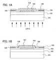
- FIGS. 1A and Bare each a cross-sectional view describing a manufacturing step of a semiconductor device relating to the present invention
- FIG. 2is a diagram describing temperature dependency of crystallization of an oxide semiconductor film of the present invention.
- FIGS. 3A to 3Care each a cross-sectional view describing a manufacturing step of a semiconductor device relating to the present invention.
- FIGS. 4A to 4Hare each a cross-sectional view describing a manufacturing step of a semiconductor device relating to the present invention.
- FIGS. 5A to 5Care each a cross-sectional view describing a manufacturing step of a semiconductor device relating to the present invention.
- FIGS. 6A to 6Fare each a cross-sectional view describing a manufacturing step of a semiconductor device relating to the present invention.
- FIG. 7is a cross sectional-view of a semiconductor device relating to the present invention.
- FIGS. 8A to 8Fare each a diagram showing a mode of a light emitting element relating to the present invention.
- FIGS. 9A to 9Fare each a diagram describing a pixel circuit of a display panel relating to the present invention and an operation configuration thereof;
- FIGS. 10A to 10Care each a diagram describing mounting of a driver circuit relating to the present invention.
- FIG. 11is a diagram describing a display module relating to the present invention.
- FIGS. 12A to 12Fare each a diagram describing one example of an electronic appliance
- FIGS. 13A and 13Bare each a cross-sectional view of a semiconductor device relating to the present invention.
- FIGS. 14A and 14Bare each a circuit diagram and a cross-sectional view of a pixel in a semiconductor device of the present invention.
- FIG. 15is a cross-sectional view of a semiconductor device relating to the present invention.
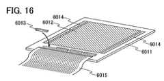
- FIG. 16is a diagram showing one mode of an element substrate in a semiconductor device of the present invention.
- FIGS. 17A and 17Bare each a diagram showing one mode of an element substrate in a semiconductor device of the present invention.
- FIGS. 18A and 18Bare each a block diagram showing a structure of a semiconductor device of the present invention.
- FIGS. 19A and 19Bare each a diagram showing a structure of an LRTA device relating to the present invention.
- FIG. 20describes one example of an electronic appliance relating to the present invention
- FIG. 21describes one example of an electronic appliance relating to the present invention.
- a manufacturing step of a TFT using a channel forming as a region of an oxide semiconductor film in which crystallinity is improved by LRTAis described with reference to FIGS. 1A and 1B .
- a base film 102is formed over a substrate 101 .
- glassor plastic (synthetic resin) such as polyethylene terephthalate (PET), polyethylene naphthalate (PEN), polyether sulfone (PES), acrylic, or polyimide can be used.
- plasticsynthetic resin
- PETpolyethylene terephthalate
- PENpolyethylene naphthalate
- PESpolyether sulfone
- acrylicacrylic
- polyimidepolyimide
- the base film 102a single layer of an insulating film such as a silicon oxide film, a silicon nitride film, a silicon oxynitride film (SiO x N y ) (x>y), or a silicon nitride oxide film (SiN x O y ) (x>y), or stacked layers thereof are used.
- the base film 102may be formed by a sputtering method or a CVD method. Note that the base film 102 is not always required to be provided, but it is preferable to form in the present invention. By forming the base film 102 , conduction of heat generated from an electrode or a wiring formed over the base film 102 to the substrate 101 can be suppressed.
- a silicon nitride oxide film with a thickness of 10 to 400 nmcan be used, for example.
- a gate electrode 103is formed over the base film 102 .
- the gate electrode 103 with a thickness of 100 to 200 nmmay be formed by a sputtering method.
- the gate electrode 103can be formed using an element selected from tantalum (Ta), tungsten (W), titanium (Ti), molybdenum (Mo), chromium (Cr), niobium (Nb), or the like, or an alloy material or a compound material mainly containing such an element.
- the gate electrode 103can also be formed with a semiconductor material typified by polycrystalline silicon doped with an impurity element such as phosphorous.
- a gate insulating film 104 with a thickness of about 50 to 500 nmis formed to cover the gate electrode 103 .
- the gate insulating film 104may be formed to have a single layer structure of a film containing an oxide of silicon or a nitride of silicon, or as a stacked layer structure thereof, by a sputtering method or a variety of CVD methods such as a plasma CVD method.
- a film containing silicon oxide (SiO x ), a film containing silicon oxynitride (SiO x N y ), or a film containing silicon nitride oxide (SiN x O y )is formed as a single layer structure, or these films are appropriately stacked to form the gate insulating film 104 .
- the gate insulating filmmay be formed by performing high density plasma treatment on the gate electrode 103 under an atmosphere containing oxygen, nitrogen, or both oxygen and nitrogen and oxidizing or nitriding a surface of the gate electrode 103 .
- the gate insulating film formed by a high density plasma treatmenthas excellent uniformity in its film thickness, film quality, and the like and the film can be formed to be dense.
- a mixed gas of a noble gas, oxygen (O 2 ), and nitrogen dioxide (NO 2 ), or dinitrogen monoxide (N 2 O); or a mixed gas of a noble gas, hydrogen (H 2 ), and oxygen (O 2 ), nitrogen dioxide (NO 2 ), or dinitrogen monoxide (N 2 O),can be used.
- a mixed gas of a noble gas and nitrogen (N 2 ) or ammonia (NH 3 ); or a mixed gas of a noble gas, hydrogen (H 2 ), and nitrogen (N 2 ) or ammonia (NH 3 )can be used.
- an oxygen radicalmay also include an OH radical
- a nitrogen radicalmay also include a NH radical
- the surface of the gate electrode 103can be oxidized or nitrided.
- the gate insulating film 104When the gate insulating film 104 is formed by performing the high density plasma treatment, the insulating film with a thickness of 1 to 20 nm, preferably 5 to 10 nm, is formed covering the gate electrode 103 . Since a reaction in this case is a solid-phase reaction, interface state density of between the gate insulating film 104 and the gate electrode 103 can be made to be extremely low. Further, since the gate electrode 103 is oxidized or nitrided directly, a thickness of the gate insulating film 104 to be formed can be uniform. Consequently, by solid-phase oxidation of the surface of the electrode by the high density plasma treatment shown here, an insulating film with favorable uniformity and low interface state density can be formed.
- an oxide of an element selected from tantalum (Ta), tungsten (W), titanium (Ti), molybdenum (Mo), chromium (Cr), niobium (Nb), or the like; or an oxide of an alloy material or a compound material mainly containing the elementfunctions as the gate insulating film 104 .
- the gate insulating film 104just an insulating film formed by the high density plasma treatment may be used, or at least one of an insulating film of silicon oxide, silicon nitride containing oxygen, silicon oxide containing nitrogen, and the like may be stacked in addition thereover by a CVD method utilizing plasma or heat reaction. Either way, transistors each of which a gate insulating film is partially or entirely an insulating film formed by high density plasma can be made to have little variations in characteristic.
- the gate insulating film 104may use the following which have favorable compatibility with the oxide semiconductor film: alumina (Al 2 O 3 ), aluminum nitride (AlN), titanium oxide (TiO 2 ), zirconia (ZrO 2 ), lithium oxide (Li 2 O), potassium oxide (K 2 O), sodium oxide (Na 2 O), indium oxide (In 2 O 3 ), yttrium oxide (Y 2 O 3 ), or calcium zirconate (CaZrO 3 ); or a material including at least two thereof.
- the gate insulating film 104may be formed as a single layer or as stacked layers of two or more layers.
- a wiring 105 with a thickness of 50 to 200 nmis formed over the gate insulating film 104 .
- a wiring materialsilver (Ag), aluminum (Al), gold (Au), copper (Cu), an alloy thereof, or the like is used. It is acceptable as long as the wiring material has higher reflectivity than that of the material used for the gate electrode 103 , and the wiring material is appropriately combined and used taking into consideration the gate electrode 103 .
- the wiringmay be formed to have a stacked layer structure. For example, aluminum and titanium may be stacked over the substrate in this order to form a wiring with a stacked layer structure. Titanium is effective in making an electrical contact property between the oxide semiconductor film and aluminum favorable.
- Titaniumalso takes on a role of suppressing diffusion of aluminum to the oxide semiconductor film.
- the wiringmay be formed with a transparent conductive film, such as for example indium tin oxide (ITO), indium tin oxide containing silicon oxide (ITSO), indium zinc oxide (IZO), indium oxide (In 2 O 3 ), tin oxide (SnO 2 ), zinc oxide (ZnO), zinc oxide added with aluminum (AlZnO), zinc oxide added with gallium (GaZnO), or zinc oxide.
- ITOindium tin oxide
- ITSOindium zinc oxide
- IZOindium oxide
- In 2 O 3tin oxide
- SnO 2tin oxide
- ZnOzinc oxide
- AlZnOzinc oxide added with gallium
- GaZnOgallium
- an oxide semiconductor film 106is formed over the gate insulating film 104 and the wiring 105 .
- zinc oxide (ZnO) in an amorphous state, a polycrystalline state, or a microcrystalline state in which both amorphous and polycrystalline states existadded with one type or a plurality of types of impurity elements selected from the following can be used: a Group 1 element (for example, lithium (Li), sodium (Na), potassium (K), rubidium (Rb), or cesium (Cs)), a Group 13 element (for example, boron (B), gallium (Ga), indium (In), or thallium (Tl)), a Group 14 element (for example, carbon (C), silicon (Si), germanium (Ge), tin (Sn), or lead (Pb)), a Group 15 element (for example, nitrogen (N), phosphorus (P), arsenic (As), antimony (Sb), or bismuth (Bi)), a
- zinc oxide (ZnO) in an amorphous state, a polycrystalline state, or a microcrystalline state in which both amorphous and polycrystalline states exist, which is not added with any impurity elementcan also be used.
- any of the followingcan also be used: InGaO 3 (ZnO) 5 , magnesium zinc oxide (Mg x Zn 1-x O), cadmium zinc oxide (Cd x Zn 1-x O), cadmium oxide (CdO), or an In—Ga—Zn—O based amorphous oxide semiconductor (a-IGZO).
- the oxide semiconductor film 106does not need to be formed under high vacuum since there is no concern for oxidation, and is inexpensive as a process.
- a plasma CVD (also called PCVD or PECVD) methodmay be used to form the film.
- CVD methodsthe plasma CVD method in particular uses a simple device, and has favorable productivity.
- LRTAis performed towards a rear surface of the substrate 101 ( FIG. 1A ).
- LRTAis performed at 250° C. to 570° C. (preferably 300° C. to 400° C., more preferably 300° C. to 350° C.) for 1 minute to 1 hour, preferably 10 minutes to 30 minutes.
- LRTAis performed with radiation from one type or a plurality types of lamps selected from a halogen lamp, a metal halide lamp, a xenon arc lamp, a carbon arc lamp, a high pressure sodium lamp, and a high pressure mercury lamp.
- a material with a relatively low melting pointcan be used if reflectivity or transmissivity of the wiring 105 is higher than that of the gate electrode 103 .
- the LRTA methodlight of a wavelength in the infrared light region, the visible light region, the ultraviolet light region, or the like can be used.
- a heating treatmentmay be performed by laser light irradiation, and for example, laser light of an infrared light laser, a visible light laser, an ultraviolet laser, or the like may be used.
- LRTA and laser light irradiationmay be combined to selectively improve crystallinity of the oxide semiconductor film.
- a continuous wave laser beam (CW laser beam) or a pulsed laser beamcan be used.
- a laser beam that can be used hereis one or a plurality of that which oscillates from a gas laser such as an Ar laser, Kr laser, or an excimer laser; a laser of which a medium is a monocrystalline YAG, YVO 4 , forsterite (Mg 2 SiO 4 ), YAlO 3 , or GdVO 4 doped with one or more of Nd, Yb, Cr, Ti, Ho, Er, Tm, and Ta, or polycrystalline (ceramic) YAG, Y 2 O 3 , YVO 4 , YAlO 3 , or GdVO 4 , doped with one or more of Nd, Yb, Cr, Ti, Ho, Er, Tm, and Ta; a glass laser; a ruby laser; an alexandrite laser; a Ti:sapphire laser; a copper vapor laser; and a
- laser light having larger energy than a band gap of the oxide semiconductor filmFor example, laser light emitted from a KrF, ArF, WeCl, or an XeF excimer laser oscillator may be used.
- the gate electrode 103is formed with a material that has lower reflectivity with respect to lamp light and that which absorbs more heat than that of the wiring 105 , the gate electrode 103 is heated to a higher temperature than the wiring 105 .
- the oxide semiconductor film 106 in a periphery of the gate electrode 103is heated; consequently, a second oxide semiconductor region 108 and a first oxide semiconductor region 107 with more favorable crystallinity than the second oxide semiconductor region 108 are formed (see FIG. 1B ).
- the gate electrode 103is irradiated with lamp light so as to be heated to around 300° C., and by that heat, the oxide semiconductor film 106 is crystallized to improve crystallinity.
- a temperature of the wiring 105is 300° C. or less even if the oxide semiconductor film 106 is crystallized.
- FIG. 1Ain a region in which the gate electrode 103 and the wiring 105 are not formed, in other words, in a region in which the substrate 101 , the base film 102 , the gate insulating film 104 , and the oxide semiconductor film 106 are stacked, lamp light is transmitted through compared to a region in which the wiring 105 and the gate electrode 103 are formed; consequently, heat is not easily absorbed and a heating temperature is lower than that of the wiring 105 . Consequently, since a large region of the substrate 101 is 350° C. or lower, shrinking does not occur easily. Note that the larger the region in which the gate electrode 103 is not formed, shrinking of the substrate 101 is suppressed.
- a semiconductor deviceis manufactured by forming an interlayer insulating film, a source electrode, a drain electrode, a pixel electrode, a light emitting element, and the like over the oxide semiconductor film 106 .
- crystallinity of a ZnO layeris improved with a heat treatment temperature of about 300° C.; therefore, compared to when a crystalline silicon film is used as a semiconductor film, the heat treatment temperature is suppressed. Also, since an oxide semiconductor film having a high light transmitting property is used and a gate electrode is selectively heated by LRTA, most of a substrate is not heated and shrinking of the substrate can be suppressed. Further, since a material used for a wiring has higher reflectivity with respect to lamp light than that of the gate electrode, crystallinity of the oxide semiconductor film can be improved even if a temperature to which the wiring is heated is suppressed to around 350° C.
- an Al wiring which has a low melting pointcan be used. Also, formation of an insulating film due to diffusion of oxygen in the oxide semiconductor film to the Al can be prevented. Since the Al wiring is inexpensive and has low resistance, a semiconductor device with favorable performance can be manufactured at low cost and with favorable productivity.
- steps of forming a base film 302 , a gate electrode 303 , and a gate insulating film 304 over a substrate 301corresponds to the steps of forming the base film 102 , the gate electrode 103 , and the gate insulating film 104 over the substrate 101 of Embodiment Mode 1, respectively; therefore, refer to Embodiment Mode 1 for the steps.
- a first oxide semiconductor film 305is formed over the gate insulating film 304 .
- zinc oxide (ZnO) in an amorphous state, a polycrystalline state, or a microcrystalline state in which both amorphous and polycrystalline states existadded with one type or a plurality of types of impurity elements selected from Group 1 elements, Group 13 elements, Group 14 elements, Group 15 elements, and Group 17 elements can be used.
- zinc oxide (ZnO) in an amorphous state, a polycrystalline state, or a microcrystalline state in which both amorphous and polycrystalline states exist, which is not added with any impurity elementcan also be used.
- any of the followingcan also be used: InGaO 3 (ZnO) 5 , magnesium zinc oxide (Mg x Zn 1-x O), cadmium zinc oxide (Cd x Zn 1-x O), cadmium oxide (CdO), or an In—Ga—Zn—O based amorphous oxide semiconductor (a-IGZO).
- zinc oxideis formed to a thickness of 50 to 200 nm (preferably 100 to 150 nm) as the first oxide semiconductor film 305 by a sputtering method.
- LRTAis performed towards a substrate surface to make crystallinity favorable ( FIG. 3A ).
- LRTAmay be performed at 250° C. to 570° C. (preferably at 300° C. to 400° C., and more preferably at 300° C. to 350° C.) for 1 minute to 1 hour, preferably 10 minutes to 30 minutes.
- LRTAis performed with radiation from one type or a plurality of types of lamps selected from a halogen lamp, a metal halide lamp, a xenon arc lamp, a carbon arc lamp, a high pressure sodium lamp, and a high pressure mercury lamp.
- lamp heatingis performed on the gate electrode 303 for 30 minutes in an oxygen atmosphere so that the gate electrode becomes about 300° C., in order to improve crystallinity of a region of the first oxide semiconductor film 305 which overlaps the gate electrode 303 with the gate insulating film therebetween. Since the first oxide semiconductor film 305 has a light transmitting property, the gate electrode 303 is heated with priority, and crystallinity of the first oxide semiconductor film 305 increases from a periphery of the gate electrode 303 towards the outside. Then, as shown in FIG. 3B , a second oxide semiconductor film including a second oxide semiconductor region 309 and a first oxide semiconductor region 308 with more favorable crystallinity than the second oxide semiconductor region 309 are formed. Note that in FIG.
- LRTAmay be performed towards a rear surface of the substrate. Since the oxide semiconductor film 305 has a light transmitting property, most region of the substrate is not easily heated even if LRTA is performed. Consequently, deformation such as shrinking of the substrate can be suppressed even if a resin with a low melting point or the like is used for the substrate. Note that crystallinity of a surface of the oxide semiconductor film and a periphery thereof may be improved directly by performing lamp heating towards the substrate surface with LRTA with increased output.
- a surface of the oxide semiconductor film on a gate insulating layer 304 side and a periphery thereofmay be crystallized with priority when performing lamp heating towards the substrate surface, by adjusting wavelength of lamp light, reflectivity of the gate electrode, and film thickness of the oxide semiconductor film, so that lamp light reflecting off of the gate electrode is absorbed by the surface of the oxide semiconductor film on the gate insulating layer 304 side and the periphery thereof.
- lamp light usedis of the visible light region to the infrared light region. Since light in these wavelength regions is not easily absorbed by the glass substrate, heating of the glass substrate can be suppressed to a minimum.
- lamp heatingmay be performed a plurality of times. By performing lamp heating a plurality of times, heating time can be gained at the same time as suppressing a rise in a temperature of the substrate.
- crystallinity of the oxide semiconductor filmmay be selectively improved by laser light irradiation, ultraviolet irradiation, or by a combination thereof.
- laser irradiationa continuous wave laser beam (CW laser beam) or a pulsed laser beam (pulse laser beam) can be used.
- a laser beam that can be used hereis one or a plurality of that which oscillates from a gas laser such as an Ar laser, Kr laser, or an excimer laser; a laser of which a medium is a monocrystalline YAG; YVO 4 , forsterite (Mg 2 SiO 4 ), YAlO 3 , or GdVO 4 doped with one or more of Nd, Yb, Cr, Ti, Ho, Er, Tm, and Ta, or polycrystalline (ceramic) YAG, Y 2 O 3 , YVO 4 , YAlO 3 , or GdVO 4 , doped with one or more of Nd, Yb, Cr, Ti, Ho, Er, Tm, and Ta; a glass laser; a ruby laser; an alexandrite laser; a Ti:sapphire laser; a copper vapor laser; and a gold vapor laser.
- a gas lasersuch as an Ar laser, Kr laser, or an excimer laser
- laser light having larger energy than a band gap of the oxide semiconductor filmFor example, laser light emitted from a KrF, ArF, XeCl, or an XeF excimer laser oscillator may be used.
- a wiring 306 and a wiring 307are formed as a source wiring and a drain wiring by performing dry etching on the Ti layer and the Al layer using photolithography and Cl 2 gas ( FIG. 3C ).
- the wirings 306 and 307are each formed to have a thickness of 10 to 200 nm by using an acceleration voltage of 1.5 kw, a pressure of 0.4 Pa, and Ar (flow rate of 30 sccm).
- the wirings 306 and 307are formed as stacked layers, if materials used for the wiring 306 and 307 have favorable compatibility with the oxide semiconductor film 305 , the wirings 306 and 307 may be formed in a single layer.
- a metalsuch as aluminum (Al), tungsten (W), molybdenum (Mo), zirconium (Zr), hafnium (Hf), vanadium (V), niobium (Nb), tantalum (Ta), chromium (Cr), cobalt (Co), nickel (Ni), platinum (Pt), titanium (Ti), or neodymium (Nd), or an alloy or a metal nitride thereof can be appropriately used.
- a material having a light transmitting propertysuch as indium tin oxide (ITO), indium zinc oxide (IZO), indium tin oxide containing silicon oxide (ITSO), indium oxide (In 2 O 3 ), tin oxide (SnO 2 ), zinc oxide (ZnO), zinc oxide added with aluminum (AlZnO), zinc oxide added with gallium (GaZnO), or the like can be appropriately used.
- a semiconductor deviceis manufactured by forming an interlayer insulating film, a wiring, a pixel electrode, a light emitting element and the like over the oxide semiconductor film 305 , the wiring 306 and the wiring 307 .
- a wiringis formed after performing LRTA on the oxide semiconductor film 305 to improve crystallinity. Therefore, a material having lower reflectivity with respect to lamp light than that of the gate electrode 303 may be used for the wiring 306 , and the material for the wiring is not limited to those mentioned in Embodiment Mode 1 as long as it has favorable compatibility with the oxide semiconductor film 305 .
- heating by LRTAmay be performed before or after processing the oxide semiconductor film 305 into a desirable shape.
- the present inventionwhen zinc oxide is used for a semiconductor film, since crystallinity of the semiconductor film improves at a heat treatment temperature of around 300° C., heat treatment temperature can be suppressed and a crystallization step can be performed at low cost compared to when a crystalline silicon film is used as the semiconductor film. Further, since a gate electrode is selectively heated by LRTA using an oxide semiconductor film having a high light transmitting property, most of a substrate is not heated and shrinking of the substrate can be suppressed.
- This embodiment modeis described with reference to FIGS. 4A to 5C .
- This embodiment modeis an example of a semiconductor device including a channel protective thin film transistor.
- a glass substrate including barium borosilicate glass, alumino borosilicate glass, or the like; a silicon substrate; a plastic substrate having heat resistance; or a resin substrateis used.
- a plastic substrate or the resin substratepolyethylene terephthalate (PET), polyethylene naphthalate (PEN), polyether sulfone (PES), acrylic, polyimide, or the like can be used.
- a surface of the substrate 400may be polished by a CMP method so that the surface is planarized. Note that an insulating layer may be formed over the substrate 400 .
- the insulating layeris formed to have a single layer structure or a stacked layer structure using at least one of an oxide material including silicon and a nitride material including silicon, by a known method such as a CVD method, a plasma CVD method, a sputtering method, or a spin coating method.
- This insulating layeris not necessarily formed, but it has effects of blocking contaminants and the like from the substrate 400 , as well as suppressing conduction of heat to the substrate.
- a conductive film 401is formed over the substrate 400 .
- the conductive film 401is processed into a desired shape and becomes a gate electrode.
- the conductive film 401is preferably formed by a method such as a printing method, an electrolytic plating method, or an evaporation method, using a material having a low reflectivity with respect to a wavelength of a light source used for LRTA heating (a material which easily absorbs heat, in other words, that which is easily heated). By using the material having a low reflectivity, a subsequent heating step becomes possible.
- a metalsuch as tungsten (W), molybdenum (Mo), zirconium (Zr), hafnium (Hf), vanadium (V), niobium (Nb), tantalum (Ta), chromium (Cr), cobalt (Co), nickel (Ni), platinum (Pt), titanium (Ti), or neodymium (Nd), or an alloy or a metal nitride thereof can be appropriately used.
- the conductive film 401may have a stacked layer structure of a plurality of these layers. Typically, a tantalum nitride film may be stacked over a substrate surface, and then a tungsten film may be stacked thereover.
- silicon added with an impurity element imparting one conductivity typemay also be used.
- an n-type silicon film of an amorphous silicon film including an impurity element imparting n-type such as phosphorus (P)can be used.
- the conductive film 401is formed to have a thickness of 10 nm to 200 nm.
- the conductive film 401is formed to have a thickness of 150 nm by a sputtering method using tungsten (W).
- a mask made of a resistis formed over the conductive film 401 using a photolithography step, and the conductive film 401 is processed into a desired shape using the mask to form a gate electrode 402 (see FIG. 4B ).
- a gate insulating film 403 a and a gate insulating film 403 bare formed over the gate electrode 402 so as to have a stacked layer structure of two layers.
- the stacked insulating filmsmay be formed consecutively in the same chamber without breaking a vacuum and under the same temperature, by changing reaction gases. By forming the insulating films consecutively without breaking the vacuum, contamination of an interface between the stacked films can be prevented.
- silicon oxide (SiO x ), silicon nitride (SiN x ), silicon oxynitride (SiO x N y ) (x>y), silicon nitride oxide (SiN x O y ) (x>y), or the likecan be appropriately used.
- the gate electrode 402may be oxidized to form an oxide film.
- the gate insualting film 403 ais preferably formed using silicon nitride (SiN x ), silicon nitride oxide (SiN x O y ) (x>y), or the like. Further, the gate insualting film 403 b is desirably formed using silicon oxide (SiO x ), silicon oxynitride (SiO x N y ) (x>y), or the like.
- the gate insulating film 403 ais formed using a silicon nitride film with a thickness of 50 nm to 140 nm that is formed with SiH 4 and NH 3 as reaction gases
- the gate insulating film 403 bis formed using a silicon oxide film with a thickness of 100 nm that is formed with SiH 4 and N 2 O as reaction gases, and stacked thereover. Note that it is preferable that the gate insulating film 403 a and the gate insulating film 403 b each have a thickness of 50 nm to 100 nm.
- the gate insulating film 403 bmay be formed using alumina (Al 2 O 3 ) or aluminum nitride (AlN) each having favorable compatibility with an oxide semiconductor film to be subsequently formed.
- aluminaAl 2 O 3
- AlNaluminum nitride
- silicon oxide, silicon nitride, silicon oxynitride, silicon nitride oxide, or the like having a high insulating property for the gate insulating film 403 aand using alumina or aluminum nitride having a favorable interface property with respect to the oxide semiconductor film for the gate insulating film 403 b , a high reliability gate insulating film can be formed.
- the gate insulating filmmay have three layers, and the third layer may be a gate insulating film using alumina or aluminum nitride.
- the oxide semiconductor film 404is formed over the gate insulating film 403 b .
- ZnO in an amorphous state, a polycrystalline state, or a microcrystalline state in which both amorphous and polycrystalline states existadded with one type or a plurality of types of impurity elements selected from Group 1 elements, Group 13 elements, Group 14 elements, Group 15 elements, and Group 17 elements can be used.
- ZnO in an amorphous state, a polycrystalline state, or a microcrystalline state in which both amorphous and polycrystalline states exist which is not added with any impurity elementcan also be used.
- any of the followingcan also be used: InGaO 3 (ZnO) 5 , magnesium zinc oxide (Mg x Zn 1-x O), cadmium zinc oxide (Cd x Zn 1-x O), cadmium oxide (CdO), or an In—Ga—Zn—O based amorphous oxide semiconductor (a-IGZO).
- ZnOmagnesium zinc oxide
- Cd x Zn 1-x Ocadmium zinc oxide
- CdOcadmium oxide
- a-IGZOIn—Ga—Zn—O based amorphous oxide semiconductor
- ZnOwhen ZnO is used for the oxide semiconductor film 404 , it is favorable that ZnO is added (doped) with nitrogen. ZnO normally shows an n-type semiconductor property. By adding nitrogen, since nitrogen works as an acceptor with respect to ZnO, a threshold voltage can be suppressed as a result.
- LRTAis performed with radiation from one or a plurality of lamps selected from a halogen lamp, a metal halide lamp, a xenon arc lamp, a carbon arc lamp, a high pressure sodium lamp, and a high pressure mercury lamp.
- LRTAis performed at 250° C. to 570° C. (preferably 300° C. to 400° C., more preferably 300° C. to 350° C.) for 1 minute to 1 hour, preferably 10 minutes to 30 minutes.
- lamp heatingis performed with a halogen lamp as a light source, and in an oxygen atmosphere at 300° C. for 30 minutes.
- the gate electrode 402is selectively heated in a short amount of time, and a first oxide semiconductor region with improved crystallinity is formed by heat thereof in a region 434 formed in a periphery of the gate electrode 402 , which is indicated by a dotted line.
- a region 424 that is not the region 434 indicated by the dotted lineis barely heated since there is little absorption of lamp light, and a second oxide semiconductor region having a different crystallinity from that of the first oxide semiconductor region (see FIG. 4E ). Consequently, since only a region in which the gate electrode 402 is formed is selectively heated and the other region is not heated, shrinking and bending of the substrate 400 can be suppressed.
- crystallinity in a periphery of the surface of the oxide semiconductor filmmay be improved directly by performing lamp heating towards the substrate surface with LRTA with increased output.
- a surface of the oxide semiconductor film on a gate insulating layer 403 b side and a periphery thereofmay be crystallized with priority when performing lamp heating towards the substrate surface, by adjusting wavelength of lamp light, reflectivity of the gate electrode, and film thickness of the oxide semiconductor film, so that lamp light reflecting off of the gate electrode is absorbed by the surface of the oxide semiconductor film on the gate insulating layer 403 b side and the periphery thereof.
- lamp light usedis of the visible light region to the infrared light region. Since light in these wavelength regions is not easily absorbed by the glass substrate, heating of the glass substrate can be suppressed to a minimum. Note that lamp heating may be performed a plurality of times. By performing lamp heating a plurality of times, heating time can be gained at the same time as suppressing a rise in a temperature of the substrate.
- crystallinity of the oxide semiconductor filmmay be selectively improved by laser light irradiation, ultraviolet irradiation, or by a combination thereof.
- laser irradiationa continuous wave laser beam (CW laser beam) or a pulsed laser beam (pulse laser beam) can be used.
- a laser beam that can be used hereis one or a plurality of that which oscillates from a gas laser such as an Ar laser, Kr laser, or an excimer laser; a laser of which a medium is a monocrystalline YAG, YVO 4 , forsterite (Mg 2 SiO 4 ), YAlO 3 , or GdVO 4 doped with one or more of Nd, Yb, Cr, Ti, Ho, Er, Tm, and Ta, or polycrystalline (ceramic) YAG; Y 2 O 3 , YVO 4 , YAlO 3 , or GdVO 4 , doped with one or more of Nd, Yb, Cr, Ti, Ho, Er, Tm, and Ta; a glass laser; a ruby laser; an alexandrite laser; a Ti:sapphire laser; a copper vapor laser; and a gold vapor laser.
- a gas lasersuch as an Ar laser, Kr laser, or an excimer laser
- laser light having larger energy than a band gap of the oxide semiconductor filmFor example, laser light emitted from a KrF, ArF, XeCl, or an XeF excimer laser oscillator may be used.
- a protective film 405is formed over the oxide semiconductor film 404 , and a resist 406 is formed over the protective film 405 (see FIG. 4F ).
- the protective film 405is processed into a desired shape to form a channel protective film 407 .
- the channel protective filmsilicon oxide (SiO x ), silicon nitride (SiN x ), silicon oxynitride (SiO x N y ) (x>y), silicon nitride oxide (SiN x O y ) (x>y), or the like can be appropriately used.
- the channel protective film 407By forming the channel protective film 407 , a semiconductor layer of a channel portion can be prevented from being etched when a source electrode and a drain electrode are formed.
- silicon nitrideis formed as the protective film 405 , and then the channel protective film 407 is formed (see FIG. 4G ).
- a mask 408is manufactured with a resist ( FIG. 4H ), and etching is performed on the oxide semiconductor film 404 to process into a desired shape by a photolithography step using the mask 408 , to form an oxide semiconductor film 409 (also called island-shaped oxide semiconductor film) ( FIG. 5A ). Note that diluted fluorinated acid is used for the etching. Subsequently, a first conductive film 411 and a second conductive film 412 are formed over the oxide semiconductor film 409 , and a mask 413 is formed by a photolithography step with a resist ( FIG. 5B ).
- the first conductive film 411 and the second conductive film 412are processed into desired shapes using the mask 413 , and first conductive films 414 a and 414 b , and second conductive films 415 a and 415 b each functioning as a source electrode or a drain electrode are formed ( FIG. 5C ).
- a commercially available resist material including a photosensitizing agentmay be used.
- a typical positive type resistsuch as a novolac resin or a naphthoquinone diazide compound which is a photosensitizing agent
- a negative type resistsuch as a base resin, diphenylsilanediol, or an acid generator may be used.
- surface tension and viscosity thereofis appropriately adjusted by adjusting a concentration of a solvent, or by adding a surfactant or the like.
- the conductive filmscan be processed into desired shapes by being subjected to direct laser light irradiation, exposure, and removal with an etchant, without forming a mask from resist. In this case, there is an advantage that a step is simplified since a mask is not required to be formed.
- the conductive material including a photosensitive substancea material including a metal such as Ag, Au, Cu, Ni, Al, or Pt, or an alloy thereof; an organic high molecular compound resin; a photo polymerization initiator; a photopolymerization monomer; and a photosensitive resin made of a solvent or the like, may be used.
- a novolac resinan acrylic copolymer, a methacrylic copolymer, a cellulose derivative, a cyclic rubber resin, or the like is used.
- one more layer of a conductive film made of for example zinc oxide added with aluminum (AlZnO) or zinc oxide added with gallium (GaZnO)may be provided as an n-type semiconductor, over the oxide semiconductor film 404 .
- AlZnOzinc oxide added with aluminum
- GaZnOgallium
- compatibility between the first conductive film 411 and the oxide semiconductor film 409becomes favorable, and a contact resistance between the oxide semiconductor film 409 and a source electrode and a drain electrode can be reduced.
- a stacked layer structure of forming Ti over GaZnO, or forming GaZnO over Timay be provided.
- a metalsuch as aluminum (Al), tungsten (W), molybdenum (Mo), zirconium (Zr), hafnium (Hf), vanadium (V), niobium (Nb), tantalum (Ta), copper (Cu), chromium (Cr), cobalt (Co), nickel (Ni), platinum (Pt), titanium (Ti), or neodymium (Nd), or an alloy or a metal nitride thereof can be appropriately used.
- the following combinations of the first conductive films 414 a , 414 b and the second conductive films 415 a , 415 bcan be considered: Ti and Al; Ta and W; TaN and Al; and TaN and Cu; as the first conductive films and the second conductive films, respectively.
- a combination of a third conductive film using Ti in addition to the first conductive films using Ti and the second conductive films using Alcan be considered.
- an AgPdCu alloymay be used for one of afirst layer and a second layer.
- a structuremay be a three-layer stacked layer structure of sequentially stacking W, an alloy of Al and Si (Al—Si), and TiN.
- tungsten nitridean alloy film of Al and Ti (Al—Ti), and Ti may be used instead of W, the alloy of Al and Si (Al—Si), and TiN, respectively.
- an elementsuch as titanium, silicon, scandium, neodymium, or copper may be added to aluminum at 0.5 to atomic %.
- a material having a light transmitting propertysuch as indium tin oxide (ITO), indium zinc oxide (IZO), indium tin oxide containing silicon oxide (ITSO), indium oxide (In 2 O 3 ), tin oxide (SnO 2 ), or zinc oxide (ZnO), or an appropriate combination thereof may be used.
- the first conductive film 411 and the second conductive film 412are formed after LRTA is performed on the oxide semiconductor film 305 and crystallinity thereof is improved. Therefore, a material having lower reflectivity with respect to lamp light than that of the gate electrode 402 may be used for the first conductive film 411 and the second conductive film 412 , and a conductive material for a wiring or an electrode is not limited to those mentioned in Embodiment Mode 1 as long as it has favorable compatibility with the oxide semiconductor film 305 .
- either plasma etching (dry etching) or wet etchingmay be employed for an etching process; however, plasma etching is suitable for treating a substrate with a large area.
- a fluorinated acid based gassuch as CF 4 , NF 3 , SF 6 , or CHF 3 ; a chlorine based gas typified by Cl 2 , BCl 3 , SiCl 4 , CCl 4 , or the like; or an O 2 gas may be used, to which an inert gas such as He or Ar may be appropriately added.
- an etching processusing atmospheric pressure discharge, electric discharge machining is possible locally, and a mask layer is not required to be formed on the an entire surface of the substrate.
- an insulating film with a thickness of about several nmmay be formed over a surface of the oxide semiconductor film.
- a bottom gate type (also called reverse staggered type) thin film transistor in which a semiconductor layer of a channel portion is not etchedcan be manufactured.
- a top gate type TFTmay be formed as long as crystallinity of at least a channel forming region of an oxide semiconductor film can be improved by heating a gate electrode that is formed over an oxide semiconductor film formed over a substrate, with a gate insulating film therebetween.
- This embodiment modecan be appropriately combined with Embodiment Modes 1 and 2.
- This embodiment modeis an example of a semiconductor device according to Embodiment Mode 3 having a channel etch type thin film transistor. Therefore, repeated description of the same portions or the portions having similar functions is omitted.
- a gate electrode 602is formed over a substrate 600 , and a gate insulating film 603 a and a gate insulating film 603 b are formed covering the gate electrode 602 ( FIG. 6A ).
- An oxide semiconductor film 620is formed over the gate insulating film 603 b , and LRTA is performed towards a substrate surface to form an oxide semiconductor film 620 including a first oxide semiconductor region 604 with improved crystallinity in a region indicated by a dotted line, and a second oxide semiconductor region 605 in which crystallization is not as progressed as the first oxide semiconductor region 604 (see FIG. 6B ).
- a mask 608is provided over the oxide semiconductor film ( FIG. 6C ), and the oxide semiconductor film is processed into a desired shape by a photolithography step to form an oxide semiconductor film 609 ( FIG. 6D ).
- a first conductive film 611 and a second conductive film 612are formed.
- a mask 613 made of a resistis formed (see FIG. 6E ).
- conductive films containing titanium and aluminumare formed by a sputtering method as each of the first conductive film 611 and the second conductive film 612 .
- first conductive film 611 and the second conductive film 612are processed into a desired shape using the mask 613 by a photolithography step, and first conductive films 615 a and 615 b , and second conductive films 616 a and 616 b each functioning as a source electrode or a drain electrode are formed ( FIG. 6F ).
- a thin film transistor in which a semiconductor layer of a part of a channel portion is etchedcan be manufactured.
- one more layer of a conductive film made of for example zinc oxide added with aluminum (AlZnO) or zinc oxide added with gallium (GaZnO)may be provided as an n-type oxide semiconductor, between the oxide semiconductor film and the first conductive film 611 .
- a stacked layer structure of forming Ti over GaZnO, or forming GaZnO over Timay be provided.
- This embodiment modecan be appropriately combined with Embodiment Modes 1 to 3.
- a light emitting devicewhich a bottom gate type thin film transistor formed in Embodiment Mode 3 or Embodiment Mode 4 is connected to a pixel electrode is described with reference to FIG. 7 .
- a thin film transistor of this embodiment modeis a channel-etched type.
- FIG. 7shows a cross-sectional view of a TFT used in a driver circuit and a cross-sectional view of a TFT used in a pixel portion.
- a reference numeral 701denotes a cross-sectional view of a TFT used in a driver circuit
- a reference numeral 702denotes a cross-sectional view of a TFT used in a pixel portion
- a reference numeral 703denotes a cross-sectional view of a light emitting element provided with a current by the TFT 702 .
- the TFTs 701 and 702are bottom gate types.
- the TFT 701 of the driver circuitincludes a gate electrode 710 formed over a substrate 700 ; a gate insulating film 711 covering the gate electrode 710 ; and an oxide semiconductor film 712 containing zinc oxide which overlaps with the gate electrode 710 with the gate insulating film 711 interposed therebetween. Further, the TFT 701 includes first conductive films 713 each functioning as a source electrode or a drain electrode, and second conductive films 714 each functioning as a source electrode or a drain electrode. Note that the first conductive films 713 and the second conductive films 714 also function as wiring.
- the gate insulating layer 711is formed of two layers of insulating films; however, the present invention is not limited to this structure.
- the gate insulating film 711may be formed with a single layer of an insulating film or three or more layers of insulating films.
- the second conductive films 714are formed with aluminum or an alloy containing aluminum. Also, the second conductive films 714 that are a pair face each other with a channel forming region of the oxide semiconductor film 712 in therebetween.
- the first conductive films 713are formed with titanium.
- the first conductive films 713are not required to be provided; however, electrical contact property of the second conductive film 711 with the oxide semiconductor film 712 becomes favorable.
- the first conductive films 713have a function as barrier layers for preventing diffusion of oxygen in the oxide semiconductor film 712 to the second conductive films 714 . As a result, reliability of a TFT can be improved. Note that an oxide semiconductor film is known to show an n-type without performing anything thereto.
- the first oxide semiconductor film in which a channel is formedmay have its conductivity type controlled in advance so as to be close to an i-type (also called as an intrinsic-type that is defined as a conductivity type having an equal number of negative and positive charges) as much as possible, by adding an impurity imparting p-type conductivity.
- an i-typealso called as an intrinsic-type that is defined as a conductivity type having an equal number of negative and positive charges
- the TFT 702 of the pixel portionincludes a gate electrode 720 formed over the substrate 700 , the gate insulating film 711 covering the gate electrode 720 , and an oxide semiconductor film 722 which overlaps with the gate electrode 720 with the gate insulating film 711 interposed therebetween. Further, the TFT 702 includes first conductive films 723 each functioning as a source electrode or a drain electrode, and second conductive films 724 each functioning as a source electrode or a drain electrode.
- the second conductive films 724are formed with aluminum or an alloy containing aluminum. Also, the second conductive films 724 that are a pair face each other with a region in which a channel of the oxide semiconductor film 722 is formed in between.
- the first conductive films 723are formed with titanium.
- the first conductive films 723are not required to be provided; however, electrical contact property of the second conductive film 724 with the oxide semiconductor film 722 becomes favorable.
- the first conductive films 723have a function as barrier layers for preventing diffusion of oxygen in the oxide semiconductor film 722 to the second conductive films 724 . As a result, reliability of a TFT can be improved.
- an oxide semiconductor filmis known to show an n-type without performing anything thereto. Therefore, the first oxide semiconductor film in which a channel is formed may have its conductivity type controlled in advance so as to be close to an i-type as much as possible, by adding an impurity imparting p-type conductivity.
- a first passivation film 740 and a second passivation film 741 each formed of an insulating filmare formed covering the TFTs 701 and 702 .
- the first passivation film 740 and the second passivation film 741can be formed by a thin film formation method such as a plasma CVD method or a sputtering method, using an insulating material such as silicon nitride, silicon oxide, silicon nitride oxide, silicon oxynitride, aluminum oxynitride, aluminum oxide, diamond-like carbon (DLC), nitrogen-containing carbon (CN), or the like.
- the passivation films covering the TFTs 701 and 702is not limited to two layers, and a single layer or three or more layers may be provided.
- the first passivation film 740 and the second passivation film 741can be formed of silicon nitride and silicon oxide, respectively.
- a passivation film of silicon nitride or silicon nitride oxideBy forming a passivation film of silicon nitride or silicon nitride oxide, entering of impurities from outside into a semiconductor element can be prevented, and degradation of the TFTs 701 and 702 due to an effect of moisture or the like can be prevented.
- the first passivation film 740 and the second passivation film 741are consecutively formed in the same chamber by performing gas switching.
- one of the second conductive films 724is connected to a pixel electrode of a light emitting element 703 .
- an insulating layer 729(also called partition, or bank) is selectively formed.
- the insulating layer 729is formed so as to have an opening portion over the pixel electrode 730 and so as to cover the second passivation film 741 .
- the insulating layer 729is formed covering an entire surface, and then etched using a mask of a resist or the like to form into a desired shape.
- the insulating layer 729can be formed with an inorganic insulating material such as silicon oxide, silicon nitride, silicon oxynitride, aluminum oxide, aluminum nitride, or aluminum oxynitride; an inorganic siloxane based insulating material having an Si—O—Si bond among compounds made of silicon, oxygen, and hydrogen, using a siloxane based material as a starting material; or an organic siloxane based material in which hydrogen bonded with silicon is substituted with an organic group such as methyl or phenyl.
- the insulating layer 729may be formed using a photosensitive or a non-photosensitive material such as an acrylic resin, or a polyimide resin.
- the insulating layer 729preferably has a form of which a curvature radius changes continuously, so that coatability of an electric field light emitting layer 731 and an opposing electrode 732 are improved.
- the electric field light emitting layer 731is formed over the pixel electrode 730 so as to be in contact therewith.
- materials showing light emission of red (R), green (G), and blue (B), respectivelyare each selectively formed by an evaporation method or the like using an evaporation mask.
- the materials showing light emission of red (R), green (G), and blue (B), respectively,are preferable since they can be formed by a droplet discharging method in a similar manner to a color filter (such as a low molecular compound or a high molecular compound), and in this case, RGB can be applied separately without using a mask.
- a color filtersuch as a low molecular compound or a high molecular compound
- RGBcan be applied separately without using a mask.
- the combinationmay be with four colors by adding emerald green.
- vermilionmay be added.
- a pixel including an EL element that emits white lightmay be combined.
- the opposing electrode 732is formed so as to be in contact with the electric field light emitting layer 731 .
- the light emitting element 703includes an anode and a cathode, one is used as a pixel electrode, and the other is used as an opposing electrode. In this way, a light emitting device having a display function using a light emitting element is completed.
- a channel forming region of an oxide semiconductor filmincludes at least a crystallized region, a TFT having higher mobility than that of a TFT using an amorphous silicon film can be obtained. Also, since a crystallization step is performed at a lower temperature than that of a TFT using a crystalline silicon film, it is inexpensive as a process.
- This embodiment modecan be appropriately combined with Embodiment Modes 1 to 4.
- Embodiment Mode 5can be referred to regarding the formation up to the second passivation film 741 ; therefore, the same reference numerals are used as those of FIG. 7 , and descriptions thereof are omitted.
- an insulating layer 1329is formed so as to cover the second passivation film 741 .
- wirings 1371 , 1372 , 1373 , and 1374 connected to the second conductive films 714 and 724 , respectively,are formed via contact holes.
- the second conductive films 724are electrically connected to a pixel electrode 1330 of a liquid crystal element 1303 via the wiring 1374 .
- the pixel electrode 1330in a case of manufacturing a transmissive type liquid crystal display panel, indium oxide containing tungsten oxide, indium zinc oxide containing tungsten oxide, indium oxide containing titanium oxide, indium tin oxide containing titanium oxide, or the like can be used.
- indium tin oxideITO
- indium zinc oxideIZO
- indium tin oxide added with silicon oxideITSO
- a metal thin film having a reflective propertya conductive film made of titanium, tungsten, nickel, gold, platinum, silver, aluminum, magnesium, calcium, lithium, an alloy thereof, or the like can be used.
- the pixel electrode 1330can be formed by an evaporation method, a sputtering method, a CVD method, a printing method, a droplet discharging method, or the like.
- an orientation film 1331is formed over the pixel electrode 1330 so as to be in contact therewith.
- an opposing electrode 1341 and an orientation film 1342are stacked in this order.
- a liquid crystal 1343is provided between the pixel electrode 1330 and the orientation film 1331 and between the opposing electrode 1341 and the orientation film 1342 , and a portion where the pixel electrode 1330 , the liquid crystal 1343 , and the opposing electrode 1341 overlap each other corresponds to a liquid crystal element 1303 .
- the pixel electrode 1330may be formed to extend over the TFT 702 , as shown in FIG. 13B .
- an oxide semiconductor filmhas a light transmitting property with respect to visible light
- a transparent conductive film including indium tin oxide (ITO), ITSO made of indium tin oxide and silicon oxide, organic indium, organic tin, zinc oxide, titanium nitride, or the like each having a light transmitting propertyan aperture ratio of a pixel portion can be improved.
- a distance (cell gap) between the pixel electrode 1330 and the opposing electrode 1341is controlled by a spacer 1361 .
- the spacer 1361is formed by processing an insulating film provided on a first substrate 700 side into a desired shape, spacers prepared separately may be dispersed over the orientation film 1331 to control the cell gap.
- a reference numeral 1362denotes a sealant, and by the sealant 1362 , the liquid crystal 1343 is sealed between the first substrate 700 and the second substrate 1340 .
- a polarizing plate 1350is provided on a surface of the first substrate 700 that is not the surface over which the TFT 701 and the TFT 702 are formed. Also, on a surface of the second substrate 1340 that is not the surface over which the opposing electrode 1341 is formed, a polarizing plate 1351 is provided. Note that the number of orientation films and polarizing plates, and positions thereof in a liquid crystal display device of the present invention are not limited to those shown in a structure of FIG. 13A .
- the present inventionsince at least crystallization of a channel forming region of an oxide semiconductor film is improved, a TFT having higher mobility than that of a TFT using an amorphous silicon film can be obtained. Also, since a crystallization step is performed at a lower temperature than that of a TFT using a crystalline silicon film, it is inexpensive as a process. Further, since crystallinity of the oxide semiconductor film is selectively increased by lamp heating, the time it takes for crystallization can be shortened compared to when the entire oxide semiconductor film is crystallized. Therefore, yield can be increased.
- the channel forming regiondoes not absorb visible light, unnecessary photocarriers are not generated. Therefore, a TFT with excellent light resistance can be formed.
- FIG. 14Ashows one mode of a circuit diagram of the pixel
- FIG. 14Bshows one mode of a cross-sectional structure of the pixel corresponding to FIG. 14A .
- a reference numeral 1501denotes a switching TFT for controlling input of video signal to the pixel
- a reference numeral 1502denotes a liquid crystal element.
- potential of a video signal that is input to the pixel via the switching TFT 1501is supplied to a pixel electrode of the liquid crystal element 1502 .
- a reference numeral 1503denotes a capacitor element for retaining voltage between the pixel electrode of the liquid crystal element 1502 and an opposing electrode when the switching TFT 1501 is turned off.
- gate electrodes of the switching TFT 1501are connected to a scanning line G, and one of a source region and a drain region is connected to a signal line S, and the other is connected to a pixel electrode 1504 of the liquid crystal element 1502 .
- One of two electrodes included in the capacitor element 1503is connected to the pixel electrode 1504 of the liquid crystal element 1502 , and the other is supplied with a constant potential, desirably a potential that is of the same level as that of the opposing electrode.
- a structureis that of a multi-gate structure in which the switching TFT 1501 is serially connected and a plurality of TFTs to which gate electrodes 1510 are connected share an oxide semiconductor film 1512 .
- an off current of the switching TFT 1501can be reduced.
- a structure of the switching TFT 1501is that of two TFTs being serially connected to each other, it may be a multi-gate structure in which three or more TFTs are serially connected to each other, and in which the gate electrodes are also connected.
- the switching TFTis not required to have a multi-gate structure, and it may be a TFT of a regular single-gate structure in which one gate electrode and one channel forming region are provided
- FIG. 15shows a cross-sectional view of a TFT used in a driver circuit, and a cross-sectional view of a TFT used in a pixel portion.
- a reference numeral 2301denotes the cross-sectional view of a TFT used in a driver circuit
- a reference numeral 2302denotes the cross-sectional view of a TFT used in a pixel portion
- a reference numeral 2303denotes a cross-sectional view of a liquid crystal element.
- the TFT 2301 of the driver circuitincludes a gate electrode 2310 formed over a substrate 2300 , a gate insulating film 2311 covering the gate electrode 2310 , and an oxide semiconductor film 2312 including a crystallized region in at least a channel forming region, that overlaps with the gate electrode 2310 with the gate insulating film 2311 therebetween.
- the TFT 2302 of the pixel portionincludes a gate electrode 2320 formed over the substrate 2300 , the gate insulating film 2311 covering the gate electrode 2320 , and an oxide semiconductor film 2322 including a crystallized region in at least a channel forming region, that overlaps with the gate electrode 2320 with the gate insulating film 2311 therebetween.
- channel protective films 2390 and 2391 formed of insulating filmsare formed so as to cover the channel forming regions of the oxide semiconductor films 2312 and 2322 .
- the channel protective films 2390 and 2391are provided to prevent the channel forming regions of the oxide semiconductor films 2312 and 2322 from getting etched during manufacturing steps of the TFT 2301 and 2302 .
- the TFT 2301includes first conductive films 2313 each functioning as a source electrode or a drain electrode and, second conductive films 2314 each functioning as a source electrode or a drain electrode; and the TFT 2302 includes first conductive films 2323 each functioning as a source electrode or a drain electrode and second conductive films 2324 each functioning as a source electrode or a drain electrode. Note that the first conductive films 2313 and 2323 , and the second conductive films 2314 and 2324 function as wirings layers.
- the gate insulating layer 2311is formed of two layers of insulating films; however the present invention is not limited to this structure.
- the gate insulating film 2311may be formed with a single layer of an insulating film or three or more layers of insulating films.
- the second conductive films 2314 and 2324are formed with aluminum or an alloy containing aluminum. Also, the second conductive films 2314 that are a pair and the second conductive films 2324 that are a pair face each other with a region in which a channel of the oxide semiconductor film 2322 is formed in between.
- the first conductive films 2313 and 2323are formed with titanium.
- the first conductive films 2313 and 2323are not required to be provided; however, electrical contact property of the second conductive films 2314 and 2324 with the oxide semiconductor films 2312 and 2322 becomes favorable.
- the first conductive films 2313 and 2323have a function as barrier layers for preventing diffusion of oxygen in the oxide semiconductor films 2312 and 2322 to the second conductive films 2314 and 2324 . As a result, reliability of a TFT can be improved.
- the oxide semiconductor films 2312 and 2322are known to show an n-type without performing anything thereto. Therefore, the first oxide semiconductor films in which channels are formed may have their conductivity type controlled in advance so as to be close to an i-type as much as possible, by adding an impurity imparting p-type conductivity.
- a first passivation film 2380 and a second passivation film 2381 each formed of an insulating filmare formed covering the TFTs 2301 and 2302 .
- the first passivation film 2380 and the second passivation film 2381can be formed by a thin film formation method such as a plasma CVD method or a sputtering method, using an insulating material such as silicon nitride, silicon oxide, silicon nitride oxide, silicon oxynitride, aluminum oxynitride, aluminum oxide, diamond-like carbon (DLC), nitrogen-containing carbon (CN), etc.
- the passivation films covering the TFTs 2301 and 2302are not limited to two layers, and a single layer or three or more layers may be provided.
- the first passivation film 2380 and the second passivation film 2381can be formed with silicon nitride and silicon oxide, respectively.
- a passivation film with silicon nitride or silicon nitride oxideBy forming a passivation film with silicon nitride or silicon nitride oxide, entering of impurities from outside into a semiconductor element can be prevented, and degradation of the TFTs 2301 and 2302 due to an effect of moisture or the like can be prevented.
- the first passivation film 2380 and the second passivation film 2381are consecutively formed in the same chamber by performing gas switching.
- an insulating layer 2329is formed covering the second passivation films 2381 .
- wirings 2371 , 2372 , 2373 , and 2374 connected to the second conductive films 2314 and 2324 , respectively,are formed via contact holes.
- the conductive film 2324is electrically connected to a pixel electrode 2330 of the liquid crystal element 2302 via the wiring 2374 .
- An orientation film 2331is formed over the pixel electrode 2330 so as to be in contact there with.
- an opposing electrode 2341 and an orientation film 2342are stacked in this order.
- a liquid crystal 2343is provided between the pixel electrode 2330 and the orientation film 2331 and between the opposing electrode 2341 and the orientation film 2342 , and a portion where the pixel electrode 2330 , the liquid crystal 2343 , and the opposing electrode 2341 overlap each other corresponds to a liquid crystal element 2303 .
- the pixel electrodemay be formed to extend over the TFT.
- ITOindium tin oxide
- ITSOmade of indium tin oxide and silicon oxide, organic indium, organic tin, zinc oxide, titanium nitride, or the like each having a light transmitting property
- an aperture ratio of a pixel portioncan be improved.
- a distance (cell gap) between the pixel electrode 2330 and the opposing electrode 2341is controlled by a spacer 2361 .
- the spacer 2361is formed by processing an insulating film into a desired shape, spacers prepared separately may be dispersed over the orientation film 2331 to control the cell gap.
- a reference numeral 2362denotes a sealant, and by the sealant 2362 , the liquid crystal 2343 is sealed between the first substrate 2300 and the second substrate 2340 .
- a polarizing plateis provided (not shown). Also, on a surface of the second substrate 2340 that is not the surface over which the opposing electrode 2341 is formed, a polarizing plate is provided (not shown). Note that the number of orientation films and polarizing plates, and positions thereof in a liquid crystal display device of the present invention are not limited to those shown in a structure of FIG. 15 .
- FIG. 16shows a mode of an element substrate in which a pixel portion 6012 formed over a first substrate 6011 is connected to a separately formed signal line driver circuit 6013 .
- the pixel portion 6012 and the scanning line driver circuit 6014are each formed using a TFT including an oxide semiconductor film including a crystallized region in at least a channel forming region.
- the signal line driver circuit 6013may be a transistor using a monocrystalline silicon semiconductor, a TFT using a polycrystalline semiconductor, or a transistor using SOI.
- the pixel portion 6012 , the signal line driver circuit 6013 , and the scanning line driver circuit 6014are each supplied with potential of a power source, various signals, and the like via an FPC 6015 .
- the signal driver circuit and the scanning line driver circuitmay both be formed over the same substrate as that of the pixel portion.
- FIG. 17Ashows a mode of an element substrate in which a pixel portion 6022 formed over a first substrate 6021 is connected to a separately formed signal line driver circuit 6023 .
- the pixel portion 6022 and the scanning line driver circuit 6024are each formed with a TFT using an oxide semiconductor film including a crystallized region in at least a channel forming region.
- the signal line driver circuit 6023is connected to the pixel portion 6022 via an FPC 6025 .
- the pixel portion 6022 , the signal line driver circuit 6023 , and the scanning line driver circuit 6024are each supplied with potential of a power source, a variety of signals, and the like via the FPC 6025 .
- FIG. 17Bshows a mode of an element substrate where an analog switch 6033 a included in the signal driver circuit is formed over a first substrate 6031 , which is the same substrate as that over which a pixel portion 6032 and a scanning line driver circuit 6034 are formed, and forming a shift register 6033 b included in the signal line driver circuit over a different substrate separately and then sticking it over the substrate 6031 .
- the pixel portion 6032 and the scanning line driver circuit 6034are each formed using the TFT including an oxide semiconductor film including a crystallized region in at least a channel forming region.
- the shift register 6033 b included in the signal line driver circuitis connected to the pixel portion 6032 via an FPC 6035 .
- the pixel portion 6032 , the analog switch 6033 a and shift register 6033 b included in the signal line drive circuit, and the scanning line driver circuit 6034are each supplied with potential of a power source, a variety of signals, and the like via the FPC 6035 .
- an entire driver circuit or a portion thereofcan be formed over the same substrate as that of a pixel portion, using the TFT including an oxide semiconductor film including a crystallized region in at least a channel forming region.
- connection method of a separately formed substrateis not particularly limited, and a COG (chip on glass) method, a wire bonding method, a TAB (tape automated bonding) method or the like can be used. Further, a connection position is not limited to the position shown in FIGS. 18A and 18B , as long as electrical connection is possible. Also, a controller, a CPU, a memory, or the like may be formed separately and connected.
- a signal line driver circuit used in the present inventionis not limited to a mode including only a shift register and an analog switch.
- another circuitsuch as a buffer, a level shifter, or a source follower may be included.
- the shift register and the analog switchis not always required to be provided, and for example a different circuit such as a decoder circuit by which selection of signal line is possible may be used instead of the shift register, and a latch or the like may be used instead of the analog switch.
- FIG. 18Ashows a block diagram of a liquid crystal display device to which the present invention is applied.
- the liquid crystal display device shown in FIG. 18Aincludes a pixel portion 801 including a plurality of pixels and provided with a liquid crystal element; a scanning line driver circuit 802 that selects each pixel; and a signal line driver circuit 803 that controls video signal input to a selected pixel.
- the signal line driver circuit 803includes a shift register 804 and an analog switch 805 .
- a clock signal (CLK) and a start pulse signal (SP)are input to the shift register 804 .
- CLKclock signal
- SPstart pulse signal
- the analog switch 805is provided with video signals.
- the analog switch 805samples the video signals according to the timing signals and distributes the video signals to a signal line of a latter stage.
- the scanning line driver circuit 802includes a shift register and a buffer 807 . Also, a level shifter may be included in some cases.
- CLKclock signal
- SPstart pulse signal
- a selection signalis generated.
- the generated selection signalis buffer amplified in the buffer 807 , and then supplied to a corresponding scanning line.
- gates of transistors in pixels of one lineare connected. Further, since the transistors in the pixels of one line have to be turned on at the same time, a buffer to which a large current can be fed is used for the buffer 807 .
- the number of terminals for connecting the shift register 804 and the analog switch 805corresponds to about 1 ⁇ 3 of the number of terminals for connecting the analog switch 805 and the pixel portion 801 . Consequently, by forming the analog switch 805 and the pixel portion 801 over the same substrate, terminals used for connecting separately formed substrates are not required as in a case of forming the analog switch 805 and the pixel portion over different substrates, and occurrence probability of poor connection can be suppressed, and yield can be increased.
- FIG. 18Bshows a block diagram of a liquid crystal display device to which the present invention is applied that is different from that of FIG. 18A .
- a pixel portion 811is shown, and a signal line driver circuit 813 includes a shift register 814 , a latch A 815 , a latch B 816 , and a D/A converter circuit (hereinafter referred to as a DAC 817 ).
- a scanning line driver circuit 812is to have the same structure as that of the scanning line driver circuit 802 in FIG. 18A
- the clock signal (CLK) and the start pulse signal (SP)are input.
- CLKclock signal
- SPstart pulse signal
- timing signalsare generated in the shift register 814 to be input in sequence to the latch A 815 of a first stage.
- video signalsare written to the latch A 815 in synchronism with the timing signals and retained.
- FIG. 18Balthough it is assumed that the video signals are written to the latch A 815 in sequence, the present invention is not limited to this structure.
- a so called division drivein which a plurality of stages of the latch A 815 are divided into several groups, and video signals are input in parallel for each group. Note that the number of the groups at this time is called a division number. For example, when the latches are divided into groups in each of four stages, this is called division driving with four divisions.
- a line periodThe time it takes for a video signal writing to a latch of the latch A 815 in all of the stages to complete is called a line period.
- a line periodsometimes includes the line period to which a horizontal retrace line period is added.
- latch signalsare supplied to the latch B 816 of a second stage, and video signals retained in the latch A 815 are written all at once in synchronism with the latch signals, and retained.
- video signals retained in the latch A 815are written all at once in synchronism with the latch signals, and retained.
- subsequent video signalsare written in sequence in synchronism with timings signals from the shift register 814 .
- video signals written and retained in the latch B 816are input to DAC 817 .
- the DAC 817converts input video signals from digital to analog, and supplies the signals to a corresponding signal line.
- FIGS. 18A and 18Bare modes of a liquid crystal display device relating to this embodiment mode, and configurations of a signal line driver circuit and a scanning line driver circuit are not limited thereto.
- FIGS. 16 to 18Bis not used just for a liquid crystal display device relating to this embodiment mode, and can be used for a light emitting device or other display devices.
- This embodimentdescribes a mode of a light emitting element used in the light emitting device described in Embodiment Mode 5, with reference to FIGS. 8A to 8F .
- FIG. 8Ashows an example of forming a first pixel electrode 11 by using a conductive film having a light transmitting property and a high work function and forming a second pixel electrode 17 by using a conductive film having a low work function.
- the first pixel electrode 11is formed of an oxide conductive material having a light transmitting property, typically, an oxide conductive material containing a silicon oxide at a concentration of 1 to 15 atomic %.
- a layer containing a light emitting substance 16composed of a hole injecting or transporting layer 41 , a light emitting layer 42 , an electron transporting or injecting layer 43 is formed over the first pixel electrode 11 .
- the second pixel electrode 17is composed of a first electrode layer 33 containing an alkali metal or an alkali earth metal such as LiF or MgAg and a second electrode layer 34 formed of a metal material such as aluminum.
- the pixel having such the structurecan emit light from the first pixel electrode 11 side as indicated by arrow in the drawing.
- FIG. 8Bshows an example of forming a first pixel electrode 11 by using a conductive film having a high work function and forming a second pixel electrode 17 by using a conductive film having a light transmitting property and a low work function.
- the first pixel electrode 11is composed of a first electrode layer 35 formed of a metal such as aluminum or titanium, or the metal and a metal material containing nitrogen at a concentration of a stoichiometric composition ratio or less, and a second electrode layer 32 formed of an oxide conductive material containing silicon oxide at a concentration of 1 to 15 atomic %.
- a layer containing a light emitting substance 16 composed of a hole injecting or transporting layer 41 , a light emitting layer 42 , an electron transporting or injecting layer 43is formed over the first pixel electrode 11 .
- the second pixel electrode 17is composed of a third electrode layer 33 containing an elemental substance of an alkali metal or an alkali earth metal such as LiF or CaF or a compound or an alloy thereof, and a fourth electrode layer 34 formed of a metal material such as aluminum.
- FIG. 8Eshows an example of emitting light from both of a first electrode and a second electrode.
- a first pixel electrode 11is formed by a conductive film having a light transmitting property and a high work function and a second pixel electrode 17 is formed by a conductive film having a light transmitting property and a low work function.
- the first pixel electrode 11is formed of an oxide conductive material including a silicon oxide at a concentration of 1 to 15 atomic % and the second electrode 17 is composed of a third electrode layer 33 containing an elemental substance of an alkali metal or an alkali earth metal such as LiF or CaF or a compound of an alloy thereof, with a thickness of 100 nm or less and a fourth electrode layer 34 formed of a metal material such as aluminum with a thickness of 100 nm or less. Accordingly, light can be emitted from both of the first pixel electrode 11 and the second electrode 17 as indicated by an arrow in the drawing.
- FIG. 8Cshows an example of forming a first pixel electrode 11 by using a conductive film having a light transmitting property and a low work function and forming a second pixel electrode 17 by a conductive film having a high work function.
- a structure of a layer containing a light emitting substanceis illustrated as a stacked layer structure formed by stacking sequentially an electron transporting or injecting layer 43 , a light emitting layer 42 , and a hole injecting or transporting layer 41 .
- the second pixel electrode 17is composed of a second electrode layer 32 formed of an oxide conductive material containing silicon oxide at a concentration of 1 to 15 atomic %, and a first electrode layer 35 formed of a metal such as aluminum or titanium, or a metal and a metal material containing nitrogen at a concentration of a stoichiometric composition ratio or less.
- the first pixel electrode 11is composed of a third electrode layer 33 containing an elemental substance of an alkali metal or an alkali earth metal such as LiF or MgAg or a compound of an alloy thereof, and a fourth electrode layer 34 formed of a metal material such as aluminum.
- FIG. 8Dshows an example of forming a first pixel electrode 11 by using a conductive film having a low work function and forming a second pixel electrode 17 by using a conductive film having a light transmitting property and a high work function.
- a structure of a layer containing a light emitting substanceis illustrated as a stacked layer structure formed by stacking sequentially an electron transporting or injecting layer 43 , a light emitting layer 42 , and a hole injecting or transporting layer 41 .
- the first pixel electrode 11is formed to have a similar structure to that illustrated in FIG. 8A and to have a thickness that enables it to reflect light generated in the layer containing a light emitting substance.
- the second pixel electrode 17is formed of an oxide conductive material containing silicon oxide at a concentration of 1 to 15 atomic %.
- a hole injecting layerby a metal oxide which is an inorganic material (typically, molybdenum oxide or vanadium oxide), oxygen which is introduced when forming the second electrode layer 32 is supplied and a hole injecting property is improved, accordingly, drive voltage can be reduced in this structure.
- a conductive film having a light transmitting propertylight can be emitted from one side of the second electrode 17 as indicated by an arrow.
- FIG. 8Fshows an example of emitting light from both sides, that is, a first pixel electrode and a second pixel electrode.
- a first pixel electrode 11is formed by a conductive film having a light transmitting property and a low work function and a second pixel electrode 17 is formed by a conductive film having a light transmitting property and a high work function.
- the first electrode 11is composed of a third electrode layer 33 containing an elemental substance of an alkali metal or an alkali earth metal such as LiF or CaF or a compound or an alloy thereof, with a thickness of 100 nm or less and a fourth electrode layer 34 formed of a metal material such as aluminum with a thickness of 100 nm or less.
- the second pixel electrode 17is formed of an oxide conductive material containing a silicon oxide at a concentration of 1 to 15 atomic %.
- the layer containing a light emitting substance 16can be formed by a charge injection transportation material and a light emitting material including an organic compound or an inorganic compound, can include one or a plurality types of layers selected from a low molecular organic compound, an intermolecular organic compound (which does not have a subliming property but have a molecular chain length of 10 ⁇ m or less as typified by dendrimer, oligomer, or the like), and a high molecular organic compound, and can be combined with an inorganic compound having an electron injecting transporting property or a hole injecting transporting property.
- a low molecular organic compoundan intermolecular organic compound (which does not have a subliming property but have a molecular chain length of 10 ⁇ m or less as typified by dendrimer, oligomer, or the like)
- a high molecular organic compoundand can be combined with an inorganic compound having an electron injecting transporting property or a hole injecting transporting property.
- metal complexes having a quinoline skeleton or a benzoquinoline skeletonsuch as tris(8-quinolinolato)aluminum (abbreviation Alq 3 ), tris(4-methyl-8-quinolinolato)aluminum (abbreviation Almq 3 ), bis(10-hydroxybenzo[h]-quinolinato)beryllium (abbreviation BeBq 2 ), and bis(2-methyl-8-quinolinolato)-4-phenylphenolato-aluminum (abbreviation BAlq) can be given.
- Alq 3tris(8-quinolinolato)aluminum
- Almq 3tris(4-methyl-8-quinolinolato)aluminum
- BeBq 2bis(10-hydroxybenzo[h]-quinolinato)beryllium
- BAlqbis(2-methyl-8-quinolinolato)-4-phenylphenolato-aluminum
- aromatic amine based compoundsi.e., one having a benzene ring-nitrogen bond
- aromatic amine based compoundssuch as 4,4′-bis[N-(1-naphthyl)-N-phenylamino]biphenyl (abbreviation ⁇ -NPD), 4,4′-bis[N-(3-methylphenyl)-N-phenylamino]biphenyl (abbreviation TPD), 4,4′,4′′-tris(N,N-diphenylamino)triphenylamine (abbreviation TDATA); and 4,4′,4′′-tris[N-(3-methylphenyl)-N-phenylamino]triphenylamine (abbreviation MTDATA) can be given.
- aromatic amine based compoundsi.e., one having a benzene ring-nitrogen bond
- TPD4,4′-bis[N-(3-methylphenyl)-N-phenyla
- alkali metal or alkaline earth metalsuch as lithium fluoride (LiF), cesium fluoride (CsF), and calcium fluoride (CaF 2 )
- LiFlithium fluoride
- CsFcesium fluoride
- CaF 2calcium fluoride
- a mixture of a highly electron transporting materialsuch as Alg a and alkaline earth metal such as magnesium (Mg) may be used.
- a metal oxidesuch as molybdenum oxide (MoO x ), vanadium oxide (VO x ), ruthenium oxide (RuO x ), tungsten oxide (WO x ), or manganese oxide (MnO) x
- MoO xmolybdenum oxide
- VO xvanadium oxide
- RuO xruthenium oxide
- WO xtungsten oxide
- MnOmanganese oxide
- phthalocyanine based compoundssuch as phthalocyanine (H 2 Pc) and copper phthalocyanine (CuPc) can be given.
- Light emitting layers 42 having different light emission wavelength bandsmay be each formed in pixels so as to perform color display.
- light emitting layers corresponding to respective luminescent colors of R (red), G (green), and B (blue)are formed.
- color puritycan be improved and specular reflection (glare) of a pixel portion can be prevented by providing a filter (coloring layer) that transmits light of a certain light emission wavelength band on a light emission side of the pixels.
- a filtercoloring layer
- a circular polarizing plate or the likewhich has been conventionally thought to be required, can be omitted, thereby reducing loss of light emitted from the light emitting layers.
- a change in huewhich is caused in the case where a pixel portion (a display screen) is seen obliquely, can be reduced.
- light emitting materialsthere are various kinds of light emitting materials that can be used for forming the light emitting layers 42 .
- low molecular organic light emitting materialsthe following substances can be used: 4-dicyanomethylene-2-methyl-6-[2-(1,1,7,7-tetramethyljulolidine-9-yl)ethenyl]-4H-pyran (abbreviation: DCJT); 2-tert-butyl-4-dicyanomethylene-6-[2-(1,1,7,7-tetramethyljulolidine-9-yl)ethenyl]-4H-pyran (abbreviation: DCJTB); periflanthene; 2,5-dicyano-1,4-bis[2-(10-methoxy-1,1,7,7-tetramethyljulolidine-9-yl)ethenyl]benzene, N,N′-dimethylquinacridone (abbreviation: DMQd); coumarin 6; coumarin 545T; tri
- a high molecular organic light emitting materialhas higher physical strength than that of a low molecular organic light emitting material, and so a light emitting element formed of a high molecular organic material has high durability. Since a high molecular organic light emitting material can be formed into a film by coating, manufacturing an element is relatively easy.
- a light emitting element structure using the high molecular organic light emitting materialis basically the same as that formed by a low molecular organic light emitting material formed by stacking sequentially a cathode, a layer containing a light emitting substance, and an anode.
- a stacked layer structure which is formed in the case of using a low molecular organic light emitting materialis difficult to be formed as a stacked layer structure composed of a layer containing a light emitting substance formed of a high molecular organic light emitting material.
- the layer containing a light emitting substanceis formed to have two stacked layers. Specifically, a structure is composed sequentially of a substrate, a layer containing a light emitting substance, a hole transporting layer, and an anode.
- emission coloris determined by a material for forming the light emitting layer
- a desired light emitting element exhibiting desired light emissioncan be formed by selecting the material.
- a high molecular light emitting material which can be used for forming the light emitting layerpolyparaphenylene vinylene based, polyparaphenylene based, polythiophene based, and polyfluorene based materials can be given.
- poly(paraphenylenevinylene)a derivative of poly(paraphenylenevinylene) (PPV): poly(2,5-dialkoxy-1,4-phenylenevinylene) (RO-PPV); poly(2-(2′-ethyl-hexoxy)-5-methoxy-1,4-phenylenevinylene) (MEH-PPV); poly(2-(dialkoxyphenyl)-1,4-phenylenevinylene) (ROPh-PPV); or the like can be given.
- PPVpoly(2,5-dialkoxy-1,4-phenylenevinylene)
- RO-PPVpoly(2-(2′-ethyl-hexoxy)-5-methoxy-1,4-phenylenevinylene)
- ROPh-PPVpoly(2-(dialkoxyphenyl)-1,4-phenylenevinylene)
- polyparaphenylene based materiala derivative of polyparaphenylene (PPP): poly(2,5-dialkoxy-1,4-phenylene) (RO-PPP); poly(2,5-dihexoxy-1,4-phenylene); or the like can be given.
- PPPpolyparaphenylene
- polythiophene based materiala derivative of polythiophene (PT): poly(3-alkylthiophene) (PAT); poly(3-hexylthiophene) (PHT); poly(3-cyclohexylthiophene) (PCHT); poly(3-cyclohexyl-4-methylthiophene) (PCHMT); poly(3,4-dicyclohexylthiophene) (PDCHT); poly[3-(4-octylphenyl)-thiophene] (POPT); poly[3-(4-octylphenyl)-2,2 bithiophene) (PTOPT); or the like can be given.
- PATpoly(3-alkylthiophene)
- PHTpoly(3-hexylthiophene)
- PCHTpoly(3-cyclohexyl-4-methylthiophene)
- PCHMTpoly(3,4-dicyclohexylthi
- PFpolyfluorene based material
- PDAFpoly(9,9-dialkylfluorene)
- PDOFpoly(9,9-dioctylfluorene)
- a hole injecting property of the anodecan be improved.
- the one which is dissolved with an acceptor material into wateris applied by a spin coating method or the like. Since the high molecular organic light emitting material having the hole transporting property is insoluble in an organic solvent, the foregoing material can be stacked over the above mentioned light emitting material having a light emitting property.
- a mixture of PEDOT and camphor sulfonic acid (CSA) as an acceptor material; a mixture of polyaniline (PANI) and polystyrenesulfonic acid (PSS) as an acceptor material; or the likecan be given.
- the light emitting layers 42can be formed to have a structure exhibiting a single color emission or white emission.
- color displaycan be realized by providing a filter (coloring layer) transmitting light at a specified wavelength at a light emission side of a pixel.
- Alq 3 , Alq 3 doped partly with Nile red which is a red emission coloring matter, Alq 3 , p-EtTAZ, and TPD (aromatic diamine)are stacked sequentially by a vapor deposition method.
- the foregoing materialis preferably coated and baked by vacuum heating.
- an aqueous solution of poly(ethylene dioxythiophene)/poly(styrenesulfonic acid) (PEDOT/PSS)which functions as a hole injecting layer, may be applied over an entire surface of a substrate and baked.
- PVKpolyvinyl carbazole
- a luminescence center pigmentsuch as 1,1,4,4-tetraphenyl-1,3-butadiene (TPB), 4-dicyanomethylene-2-methyl-6-(p-dimethylamino-styryl)-4H-pyran (DCM1), Nile red, or coumarin 6
- TPB1,1,4,4-tetraphenyl-1,3-butadiene
- DCM14-dicyanomethylene-2-methyl-6-(p-dimethylamino-styryl)-4H-pyran
- Nile redor coumarin 6
- the light emitting layercan be formed by a single layer.
- 1,3,4-oxadiazole derivatives (PBD) having an electron transporting propertycan be dispersed to polyvinylcarbazole (PVK) having a hole transporting property.
- PVKpolyvinylcarbazole
- white emissioncan be obtained by dispersing PBD of 30 wt % as an electron transporting agent and dispersing an appropriately amount of four kinds coloring matters (TPB, coumarin 6, DCM1, and Nile red).
- TPBtrifluorous carbonate
- TPBcoumarin 6, DCM1
- Nile redcoloring matters
- Besides the light emitting element exhibiting white emission, light emitting elements exhibiting red emission, green emission, or blue emissioncan be manufactured by appropriately selecting a material of the light emitting layer.
- a hole injecting property of the anodecan be improved.
- a high molecular organic material having a hole transporting property dissolved in water together with an acceptor materialis coated by a spin coating method. Since the high molecular organic material having a hole transporting property is insoluble in an organic solvent, the foregoing material can be stacked over the above mentioned light emitting material having a light emitting property.
- a mixture of PEDOT and camphor sulfonic acid (CSA) as an acceptor material; a mixture of polyaniline (PANT) and polystyrenesulfonic acid (PSS) as an acceptor material; or the likecan be given.
- a triplet excited material including metal complexescan be used besides a singlet excited light emitting material.
- a red luminescent pixelwhich has a relatively short half-brightness life is formed by a triplet excited light emitting material among the red luminescent pixel, a green luminescent pixel, and blue luminescent pixel; and the other pixels are formed by a singlet excited light emitting material. Since a triplet excited light emitting material has good emission efficiency, there is an advantage of obtaining luminescence which can be obtained in the case of using a singlet excited light emitting material at low power consumption.
- a light emitting elementcan be operated at a small amount of current in the case of applying a triplet excited light emitting material for a red emission pixel.
- a red luminescent pixel and a green luminescent pixelare formed by a triplet excited light emitting material, and a blue luminescent pixel can be formed by a singlet excited light emitting material.
- a green luminescent pixelwhich is well visible for human by a triplet excited light emitting material, power consumption can be further reduced.
- a material using metal complexes as a dopantcan be nominated.
- the followingare known as the foregoing metal complexes: metal complexes having platinum which is the third transition series element as a central metal, metal complexes having iridium as a central metal, or the like. These compounds are not limited as a triplet excited light emitting material.
- a compound having the foregoing structure and a compound having Group 8 to Group 10 elements as a central metalcan be used.
- a light emitting elementcan be formed by appropriately stacking functional each layer such as a hole injecting transporting layer, a hole transporting layer, an electron injecting transporting layer, an electron transporting layer, a light emitting layer, an electron blocking layer, or a hole blocking layer. Further, a mixed layer or mixed junction can be formed by combining each of the foregoing layers. A layer structure of the light emitting layer is variable.
- a pixel circuit of a display panel of a light emitting device relating to the present invention and an operational configuration thereofis described with reference to FIGS. 9A to 9F .
- the operational configuration of the display panel in a display device in which video signals are digitalthere is a configuration in which video signals to be input to a pixel is regulated by voltage, and a configuration in which they are regulated by current.
- As the configuration in which video signals are regulated by voltagethere is one where voltage applied to a light emitting element is constant (CVCV), and one where current applied to the light emitting element is constant (CVCC).
- CCCVvoltage applied to the light emitting element
- CCCCcurrent applied to the light emitting element
- a signal line 3710 and a power source line 3711are arranged in a column direction and a scanning line 3714 is arranged in a row direction. Also, a switching TFT 3701 , a driving TFT 3703 , a capacitor element 3702 , and a light emitting element 3705 are included.
- the switching TFT 3701 and the driving TFT 3703are operated in a linear region when they are turned on. Also, the driving TFT 3703 has a role of controlling whether voltage is applied to the light emitting element 3705 . It is favorable in terms of a manufacturing step if both TFTs have the same conductivity type.
- the switching TFT 3701is formed as an n-channel type TFT
- the driving TFT 3703is formed as a p-channel type TFT.
- a depletion type TFTmay be used in addition to an enhancement type TFT.
- a ratio (W/L) of a channel width W and a channel length L of the driving TFT 3703is preferably 1 to 1000, even though it depends on a mobility of the TFT. As W/L gets larger, an electrical property of the TFT is improved.
- the switching TFT 3701controls input of video signals to the pixel, and when the switching TFT 3701 is turned on, video signals are input inside the pixel. Then, voltage of the video signals is retained in the capacitor element 3702 .
- FIG. 9Ain a case where the power source line 3711 is Vss and an opposing electrode of the light emitting element 3705 is Vdd, as in FIGS. 8C and 8D , the opposing electrode of the light emitting element is an anode, and an electrode connected to the driving TFT 3703 is a cathode. In this case, luminance irregularity due to characteristic variation of the driving TFT 3703 can be suppressed.
- FIG. 9Ain a case where the power source line 3711 is Vdd and the opposing electrode of the light emitting element 3705 is Vss, as in FIGS. 8A and 8B , the opposing electrode of the light emitting element is a cathode, and the electrode connected to the driving TFT 3703 is an anode.
- the opposing electrode of the light emitting elementis a cathode
- the electrode connected to the driving TFT 3703is an anode.
- the pixel shown in FIG. 9Bhas the same pixel configuration as that shown in FIG. 9A except that in FIG. 9B , a TFT 3706 and a scanning line 3715 are added.
- Turning on or off of the TFT 3706is controlled by the newly placed scanning line 3715 .
- the TFT 3706When the TFT 3706 is turned on, a charge retained in the capacitor element 3702 is discharged, and the driving TFT 3703 is turned off.
- the TFT 3706can be called an erasing TFT. Consequently, in the configuration in FIG. 9B , a duty ratio of light emission can be improved since a lighting period can be started at the same time as or right after a start of a writing period, without waiting for signals to be written to all pixels.
- a current value of the light emitting element 3705can be determined by the driving TFT 3703 which operates in the linear region.
- the pixel shown in FIG. 9Chas a pixel configuration shown in FIG. 9A with a power source line 3712 and a current control TFT 3704 provided in addition.
- the pixel shown in FIG. 9Ehas the same configuration as the pixel shown in FIG. 9C , except that a gate electrode of the driving TFT 3703 is connected to the power supply line 3712 arranged in a row direction.
- both pixels shown in FIGS. 9 c and 9 Eshow the same equivalent circuit schematic.
- the power supply line 3712 arranged in a column direction( FIG. 9C ) is formed with a conductive film formed in a different layer from that of the power supply line 3712 arranged in a row direction ( FIG. 9E ).
- wirings to which the gate electrode of the driving TFT 3703 are connectedis given focus, and in order to show that layers for manufacturing the wirings are different, they are separately described in FIGS. 9C and 9E .
- the switching TFT 3701operates in the linear region
- the driving TFT 3703operates in a saturation region.
- the driving TFT 3703has a role of controlling a current value fed to the light emitting element 3705
- the current control TFT 3704operates in the saturation region has a role of controlling supply of current to the light emitting element 3705 .
- the pixel shown in each of FIGS. 9D and 9Fhave the same pixel configuration as the pixel shown in each of FIGS. 9C and 9E , respectively, except that they are each provided with an erasing TFT 3706 and the scanning line 3715 in addition.
- Vdd and Vsscan be appropriately changed depending on a direction in which current of a light emitting element flows.
- the current control TFT 3704since the current control TFT 3704 operates in the linear region, a small shift in Vgs of the current control TFT 3704 does not have an effect on the current value of the light emitting element 3705 .
- the current value of the light emitting element 3705can be determined by the driving TFT 3703 which operated in the saturation region.
- the present inventionis not limited thereto, and in a case where a capacity for retaining video signals can be covered by a gate capacitance, the capacitor element 3702 is not required to be provided.
- a driving method of a screen displayis not particularly limited, and for example, a dot sequential driving method, a line sequential driving method, an area sequential driving method, or the like may be used.
- the line sequential driving methodis used, and a time division gray scale driving method or an area gray scale driving method may be appropriately used.
- image signals input to a source line of the display devicemay be analog signals, or digital signals, and a driver circuit and the like may be designed appropriately according to the image signals.
- FIGS. 10A to 10Cmounting of a driver circuit relating to the present invention is described with reference to FIGS. 10A to 10C .
- a signal line driver circuit 1402 and scanning line driver circuits 1403 a and 1403 bare mounted on a periphery of a pixel portion 1401 .
- an IC chip 1405is mounted on a substrate 1400 by a known mounting method such as a method using an anisotropic conductive adhesive or an anisotropic conductive film, a COG method, a wire bonding, a reflow treatment using a solder bump, or the like.
- the IC chip 1405is mounted by a COG method, and connected to an external circuit through an FPC (flexible printed circuit) 1406 .
- the pixel portion 1401 , the scanning line driver circuits 1403 a and 1403 b , and the likemay be integrated over the substrate while the signal line driver circuit 1402 and the like may be separately mounted as IC chips.
- the IC chip 1405 as the signal line driver circuit 1402is mounted on the substrate 1400 by a COG method.
- the IC chip 1405is connected to an external circuit through the FPC 1406 .
- the signal line driver circuit 1402 and the likeare mounted by a TAB method instead of a COG method.
- the IC chipis connected to an external circuit through the FPC 1406 .
- the signal line driver circuitis mounted by a TAB method in FIG. 10C
- the scanning line driver circuitmay be mounted by a TAB method.
- the pixel portioncan occupy a large area in the substrate, leading to a narrower frame.
- an IC(hereinafter referred to as a driver IC) formed over a glass substrate may be provided. Since an IC chip is formed over a circular silicon wafer, the shape of a mother substrate is limited. Meanwhile, a driver IC is formed over a glass substrate whose shape is not limited, which results in increased productivity. Accordingly, the shape and size of a driver IC can be set freely. For example, when forming a driver IC with a long side of 15 to 80 mm, a smaller number of driver ICs are required as compared to the case of mounting IC chips. As a result, the number of connection terminals can be reduced and productive yield can be increased.
- a driver ICcan be formed using a crystalline semiconductor formed over a substrate, and the crystalline semiconductor may be formed by continuous wave laser light irradiation.
- a semiconductor film obtained by continuous wave laser light irradiationhas few crystal defects and large crystal grains. Accordingly, a transistor having such a semiconductor film is improved in mobility and response speed, capable of high speed driving, and suitable for a driver IC.
- a driver ICmay be formed using an oxide semiconductor film of the present invention in which crystallinity of at least a channel forming region is improved.
- a display module relating to the present inventionis described.
- a liquid crystal moduleis described with reference to FIG. 11 .
- a substrate 1601 and an opposing substrate 1602are stuck together by a sealant 1600 , and a pixel portion 1603 and a liquid crystal layer 1604 are provided therebetween to form a display region.
- a coloring layer 1605is required in a case of performing color display, and in a case of an RGB method, a coloring layer corresponding to each of red, green and blue are provided corresponding to each pixel.
- polarizing plates 1606 and 1607are provided, respectively.
- a protective film 1616is formed, and alleviates impact from the exterior.
- a wiring substrate 1610is connected to a connection terminal 1608 provided over the substrate 1601 via an FPC 1609 .
- External circuits 1612such as a pixel driver circuit (an IC chip, a driver IC, or the like), a control circuit, a power source circuit or the like is incorporated to the wiring substrate 1610 .
- a cold cathode tube 1613 , a reflecting plate 1614 , and an optical film 1615are a backlight unit, and these become a light source to emit light to a liquid crystal display panel.
- a liquid crystal panel, the light source, the wiring substrate, the FPC, and the likeare retained and protected in a bezel 1617 .
- a television devicealso simply called a TV, or a television receiving device
- a digital cameraalso simply called a digital video camera
- a mobile phone devicealso simply called a cellular phone device or a cellular phone
- a mobile information terminalsuch as a PDA, a mobile game machine, a monitor for a computer, a computer, an audio reproducing device such as a car audio component, an image reproducing device such as a home-use game machine provided with a recording medium, or the like
- an audio reproducing devicesuch as a car audio component
- an image reproducing devicesuch as a home-use game machine provided with a recording medium, or the like
- the mobile information terminal shown in FIG. 12Aincludes a main body 9201 , a display portion 9202 , and the like.
- the mobile information terminalcan be provided inexpensively.
- the digital video camera shown in FIG. 12Bincludes a display portion 9701 , a display portion 9702 , and the like.
- the digital video cameracan be provided inexpensively.
- the mobile terminal shown in FIG. 12Cincludes a main body 9101 , a display portion 9102 , and the like. Embodiment Modes 1 to 5, and embodiments 1 to 4 can be applied to the display portion 9102 . By using the display device that is one feature of the present invention, the mobile terminal can be provided inexpensively.
- the mobile type television device shown in FIG. 12Dincludes a main body 9301 , a display portion 9302 , and the like.
- the display devicethat is one feature of the present invention, the mobile type television device can be provided inexpensively.
- the present inventioncan be widely applied to a small scale television device such as a television device mounted on a mobile terminal such as a cellular phone, a medium scale television device that can be carried around, and a large scale television device (for example, 40-inch or larger).
- the mobile type computer shown in FIG. 12Eincludes a main body 9401 , a display portion 9402 , and the like.
- the display devicethat is one feature of the present invention, the mobile type computer can be provided inexpensively.
- the television device shown in FIG. 12Fincludes a main body 9501 , a display portion 9502 , and the like.
- the television devicecan be provided inexpensively.
- FIGS. 19A and 19Ba structure of an LRTA device used in the present invention is described with reference to FIGS. 19A and 19B .
- a gate electrode 1922 , a gate insulating films 1923 a and 1923 b , and an oxide semiconductor film 1902are formed over a glass substrate 1901 .
- an infrared light lamp 1903 and an ultraviolet light lamp 1904are provided, respectively.
- a first infrared light auxiliary lamp 1905 , and a second infrared light auxiliary lamp 1906are provided in parallel with the ultraviolet light lamp 1904 . Note that the first infrared light auxiliary lamp 1905 and the second infrared light auxiliary lamp 1906 are not required to be provided.
- this embodiment modehas a structure in which the first infrared light auxiliary lamp 1905 and the second infrared light auxiliary lamp 1906 are placed in front and in back (with respect to a moving direction of the substrate) of the ultraviolet light lamp 1904 , respectively.
- the structuremay be that both are placed in the front or in the back.
- each lampmoves in a direction of an arrow in FIG. 19A , and scans a linear light.
- a region 1908 shown by a dotted line in the oxide semiconductor film 1902 that overlaps with the gate electrode 1922 with the gate insulating films 1923 a and 1923 b therebetweenis irradiated with infrared light from the first infrared light auxiliary lamp 1905 to be heated.
- each lampis moved when lamp irradiation is performed on the substrate; however, the glass substrate may be moved, or both the lamp and the substrate may be moved.
- the upper surface side of the substrateis irradiated with ultraviolet light from the ultraviolet light lamp 1904 , as well as the lower surface side of the substrate is irradiated with infrared light from the infrared light lamp 1903 , and the region 1908 of the oxide semiconductor film 1902 that overlaps with the gate electrode 1922 is heated.
- crystallization of the oxide semiconductor film 1902is performed with this region 1908 having priority.
- the region 1908 heated by irradiation with the ultraviolet light lamp 1904 and the infrared light lamp 1903is heated with infrared light from the second infrared light auxiliary lamp 1906 that is placed in back of the ultraviolet light lamp 1904 .
- Irradiation with infrared light from the second infrared light auxiliary lamp 1906is provided to further heat the region 1908 in which crystallization is promoted.
- the region 1908 of the oxide semiconductor film 1902(the region that becomes a crystalline oxide semiconductor film by a crystallization step) that overlaps with the gate electrode 1922 appears to move to the front along with a movement of the substrate.
- FIG. 19Bshows a graph showing a relationship between time (Time) and temperature (Temp.) of the region 1908 of the oxide semiconductor film 1902 .
- the region 1908comes to a preheating state, then continues on to a main heating state, and a post heating state, with passing of time.
- a temperatureis raised to a certain degree so that a temperature gradient with the subsequent main heating state is alleviated. This is so that accumulation of warping energy and the like in the oxide semiconductor film due to being heated suddenly in the main heating state, is prevented.
- output energy of the first infrared light auxiliary lamp 1905is set to be smaller than output energy of the infrared light lamp 1903 .
- a practitionermay decide how adjustment is to be made to form the appropriate temperature gradient.
- infrared light irradiationis performed towards a lower surface side of the substrate, and the oxide semiconductor film 1902 is brought to the main heating state in which a film surface temperature is raised to 250° C. to 570° C.
- crystallinity of the region 1908 in the oxide semiconductor film 1902becomes favorable. Note that ultraviolet light emitted at the same time contributes to electron excitation; therefore, it does not contribute to change in terms of heat.
- the region 1908 with improved crystallinity obtained in the main heating stateis heated by the second infrared auxiliary lamp 1906 placed in back of the ultraviolet light lamp 1904 .
- This post heating statehas a role of preventing a completion of crystallization in a state where thermal equilibrium is deteriorated by sudden cooling in the main heating state.
- Thisis a device for obtaining the most stable bond state by providing allowance in a time period required for crystallization.
- output energy of the second infrared light auxiliary lamp 1906is also set to be smaller than that of infrared light lamp 1903 placed under a substrate surface, and adjusted so that a temperature gradient is formed in which the temperature is gradually lowered.
- shrinking of a substratecan be suppressed since a portion of an oxide semiconductor film that overlaps with a gate electrode is heated. Also, by performing crystallization by moving each lamp or substrate, throughput can be increased. Also, occurrence of a crystal defect such as stress warping, a dangling bond, or the like that can occur due to sudden heating of an oxide semiconductor film or sudden cooling of a crystalline oxide semiconductor film can be suppressed, and the oxide semiconductor film including the region 1908 with excellent crystallinity can be obtained.
- heating of the substratemay be suppressed.
- the electrophoresis display device shown in FIG. 20includes a main body 2010 , a pixel portion 2011 displaying an image, a driver IC 2012 , a receiving device 2013 , a film battery 2014 , and the like.
- Each of the driver IC 2012 , the receiving device 2013 , and the likemay be mounted with a semiconductor part.
- the semiconductor device of the present inventioncan be used for the pixel portion 2011 and the driver IC 2012 .
- the pixel portion 2011has a structure where a display layer in which microcapsules, Gyricon beads, and the like are arranged and a driver layer controlling the display layer are stacked. The display layer and the driver layer are interposed between two plastic films.
- Such an electrophoresis display deviceis also called an electronic paper, and it is extremely light weight, and since it has a flexible property, it can be rolled up in a tubular form; consequently, it is extremely advantageous in carrying around. Therefore, a display medium of a large screen can be freely carried around. Also, since the semiconductor of the present invention is used for the pixel portion 2011 and the like, an inexpensive display device can be provided.
- the electrophoresis display device of this embodimentis a device in which a plurality of microcapsules each including first particles having a positive charge and second particles having a negative charge are dispersed in a solvent or a solute, and an electrical field is applied to the microcapsules so that the particles in the microcapsules move in opposite directions of each other, and only a color of the particles gathered on one side is displayed.
- the first particles or the second particlesincludes a colorant, and does not move in a case where there is not electric field.
- a color of the first particlesis different from a color of the second particles (the particles may also be colorless). That which microcapsules are dispersed in a solvent is called an electronic ink, and this electronic ink can be printed on a surface such as glass, plastic, fabric, paper, and the like.
- ITOindium tin oxide
- ITSOmade of indium tin oxide and silicon oxide, organic indium, organic tin, zinc oxide, titanium nitride, or the like each having a light transmitting property with respect to visible light for a source electrode, a drain electrode, and the like.
- the semiconductor device of the present inventioncan be used as a means for displaying mainly still images for a navigation system, an audio reproducing device (such as a car audio component, or an audio component), a personal computer, a game machine, a mobile information terminal (such as a mobile computer, a cellular phone, a mobile game machine, or an electronic book), and in addition, the semiconductor device can be used for household appliances such as a refrigerator, a washing machine, a rice cooker, a fixed telephone, a vacuum cleaner, and a clinical thermometer, as well as for a hanging poster in a train, and a large-sized information display such as an arrival and departure guide board in a railroad station and an airport.
- an audio reproducing devicesuch as a car audio component, or an audio component
- a personal computersuch as a personal computer, a game machine, a mobile information terminal (such as a mobile computer, a cellular phone, a mobile game machine, or an electronic book)
- the semiconductor devicecan be used for household appliances such as a refrigerator,
- the digital audio player shown in FIG. 21includes a main body 2110 , a display portion 2111 , a memory portion 2112 , an operation portion 2113 , a pair of earphones 2114 , and the like. Note that instead of the pair of earphones 2114 , a pair of headphones, or a wireless pair of earphones can be used.
- the display portion 2111liquid crystal, organic EL, or the like can be used.
- the memory portion 2112a flash memory with a recording capacity of 200 megabytes (MB) to 200 gigabytes (GB) is used, and by operating the operation portion 2113 , an image or a sound (music) can be recorded and reproduced.
- a channel forming region of an oxide semiconductor film of a TFT included in a semiconductor device of the present inventionincludes at least a crystallized region, by providing the semiconductor device of the present invention to the display portion 2111 , an inexpensive digital audio player with good performance can be provided. Further, since the channel forming region of the oxide semiconductor film is transparent and does not absorb visible light, unnecessary light carriers are not generated. Therefore, since characteristic degradation of the channel forming region due to light irradiation does not occur, a highly reliable digital audio player can be provided.
Landscapes
- Engineering & Computer Science (AREA)
- Physics & Mathematics (AREA)
- General Physics & Mathematics (AREA)
- Computer Hardware Design (AREA)
- Condensed Matter Physics & Semiconductors (AREA)
- Manufacturing & Machinery (AREA)
- Microelectronics & Electronic Packaging (AREA)
- Power Engineering (AREA)
- Optics & Photonics (AREA)
- Health & Medical Sciences (AREA)
- Nonlinear Science (AREA)
- Electromagnetism (AREA)
- Toxicology (AREA)
- Chemical & Material Sciences (AREA)
- Chemical Kinetics & Catalysis (AREA)
- Molecular Biology (AREA)
- Life Sciences & Earth Sciences (AREA)
- Electrochemistry (AREA)
- Thin Film Transistor (AREA)
- Liquid Crystal (AREA)
- Electroluminescent Light Sources (AREA)
- Recrystallisation Techniques (AREA)
- Electrodes Of Semiconductors (AREA)
- Devices For Indicating Variable Information By Combining Individual Elements (AREA)
- Electrochromic Elements, Electrophoresis, Or Variable Reflection Or Absorption Elements (AREA)
- Crystallography & Structural Chemistry (AREA)
- Dram (AREA)
- Physical Vapour Deposition (AREA)
- Formation Of Insulating Films (AREA)
Abstract
Description
This application is a continuation of U.S. application Ser. No. 11/524,549, filed on Sep. 21, 2006 now U.S. Pat. No. 7,674,650.
1. Field of the Invention
The present invention relates to a semiconductor device and a manufacturing method thereof and particularly relates to a semiconductor device using an oxide semiconductor. The present invention also relates to an electronic appliance equipped with the semiconductor device.
2. Description of the Related Art
Flat panel displays (FPD), typified by liquid crystal displays (LCD) and EL displays, have attracted attention as the display device replacing conventional CRTs. The development of large screen liquid crystal television mounted with an active matrix-driven large scale liquid crystal panel is particularly an important challenge which liquid crystal panel makers should focus on. In addition, large screen EL television is also being developed.
In the conventional liquid crystal device or electroluminescence display device (hereinafter referred to as a light emitting display device or an EL display device), a thin film transistor (hereinafter referred to as TFT) is used, which uses crystalline silicon or amorphous silicon as a semiconductor element driving each pixel.
A TFT using a crystalline silicon film has a higher mobility by two digits or more compared to a TFT using an amorphous silicon film, and has potential for high speed operation when it is used for a scanning line driver circuit for selecting a pixel of a light emitting display device, a signal line driver circuit for sending video signals to a selected pixel, or the like. However, using crystalline silicon for a semiconductor film complicates manufacturing steps because of crystallization of the semiconductor film compared to using amorphous silicon for the semiconductor film; therefore, there are drawbacks of yield decrease by that much and increase in cost. Further, a heating temperature for the crystallization is 550° C. or higher, and it is difficult to use a substrate made of a resin with low melting point, a plastic substrate, or the like.
On the other hand, the TFT using amorphous silicon for a semiconductor film can be manufactured at low cost, since it is not heated at a high temperature and a resin substrate or a plastic substrate can be used. However, a mobility of only around 0.2 to 1.0 cm2/V·s at most can be obtained with a TFT of which a channel forming region is formed with a semiconductor film formed of amorphous silicon, and it also has high power consumption.
A plasma CVD method is commonly used when an amorphous silicon film is formed over a substrate. Film formation by a plasma CVD method requires heating under high vacuum, and damage to a plastic substrate or an organic resin film over a substrate is a concern. In addition to the concern in forming the amorphous silicon film by a plasma CVD method, there is also a concern in forming the film by a sputtering method which is that a thin insulating film might be formed over a surface of an amorphous silicon film when the amorphous silicon film is exposed to atmospheric air.
As a material to replace a semiconductor made of such silicon, forming a TFT using an oxide semiconductor such as zinc oxide for a channel forming region has been reported in recent years (for example, refer to Patent Document 1: Japanese Patent Laid-Open No. 2000-150900, and Non-Patent document 1: Elvira M. C. Fortunato, et al. Applied Physics Letters, Vol. 85, No. 13, P2541 (2004)). Since the oxide semiconductor has mobility equal to or higher than that of a TFT formed with a semiconductor including amorphous silicon, further characteristic improvement is demanded.
In view of the foregoing problems, an object of the present invention is to provide a semiconductor device including a semiconductor element with improved characteristics and a manufacturing method thereof.
On another front, size increase in substrate has advanced for manufacturing a large-area device by a cheaper process, as in liquid crystal television. However, with the size increase in substrate, there is a problem of being easily effected by bending and warping. Also, when a substrate is heated to a high temperature during a heat treatment step, a size of the substrate becomes distorted due to warping and shrinking, and there is a problem of a decrease in precision of alignment in a photolithography step.
Consequently, an object of the present invention is to provide a technique that makes it possible to manufacture with good yield a semiconductor device over a large substrate, having for example a side longer than 1 meter, in a crystallization step of a semiconductor element used in a semiconductor device.
As mentioned above, an object of the present invention is to provide a semiconductor device including a semiconductor element with characteristics that are further improved, which can be manufactured at lower cost and more favorable productivity than before.
In the present invention, a compound semiconductor, more preferably an oxide semiconductor is used as a semiconductor. As the oxide semiconductor, for example, zinc oxide (ZnO), InGaO3(ZnO)5, magnesium zinc oxide (MgxZn1-xO), cadmium zinc oxide (CdxZn1-xO), cadmium oxide (CdO), an In—Ga—Zn—O based amorphous oxide semiconductor (a-IGZO), or the like is used. Also, the gist of the present invention is that by heating a gate electrode that is near the compound semiconductor by lamp rapid thermal annealing (LRTA; also simply called lamp heating), crystallization of the compound semiconductor is selectively promoted, and a TFT using a compound semiconductor having the region in which crystallization is promoted at least in a channel region can be manufactured.
One feature of the present invention is to have a gate electrode formed over a substrate, an insulating film formed covering the gate electrode, and an oxide semiconductor film formed over the insulating film. The oxide semiconductor film includes a first oxide semiconductor region and a second oxide semiconductor region, and the first oxide semiconductor region that is formed in a position which overlaps with the gate electrode has higher crystallinity than the second semiconductor region. Note that “crystallinity” expresses a degree of regularity of atomic arrangement inside of crystal, and when manufacturing a TFT using an oxide semiconductor film with favorable crystallinity (also expressed as having high crystallinity or with improved crystallinity), an electrical characteristic thereof is favorable.
One feature of the present invention is to have a gate electrode and an oxide semiconductor film over a substrate. In a region of the oxide semiconductor film which overlaps with the gate electrode via an insulating film, a portion of the region is crystallized.
One feature of the present invention is to have a gate electrode, an oxide semiconductor film, and a conductive film over a substrate. The conductive film is provided to be in contact with the oxide semiconductor film, and in a region of the oxide semiconductor film which overlaps with the gate electrode via an insulating film, a portion of the region is crystallized.
One feature of the present invention is to have a gate electrode over a substrate, an insulating film formed covering the gate electrode, and an oxide semiconductor film formed over the insulating film. The oxide semiconductor film is crystallized in at least a region which overlaps with the gate electrode. Note that “crystallization” refers to generation of crystal nuclei from an amorphous state, or growth of crystal grains from a state in which crystal nuclei have been generated.
One feature of the present invention is to have a gate electrode formed over a substrate, an insulating film formed covering the gate electrode, a conductive film formed over the insulating film, and an oxide semiconductor film formed over the insulating film and the conductive film. The oxide semiconductor film is crystallized in at least a region which overlaps with the gate electrode.
One feature of the present invention is to have a gate electrode formed over a substrate, an insulating film formed covering the gate electrode, a conductive film formed over the insulating film, and an oxide semiconductor film formed over the insulating film and the conductive film. The gate electrode has lower reflectivity with respect to a light source used for crystallization than the conductive film. Note that reflectivity comparison is used when the conductive film is a metal film or the like having a light shielding property.
One feature of the present invention is to have a gate electrode formed over a substrate, an insulating film formed covering the gate electrode, a conductive film formed over the insulating film, and an oxide semiconductor film formed over the insulating film and the conductive film. The gate electrode has higher heat absorption rate than the conductive film.
One feature of the present invention is to have a gate electrode formed over a substrate, an insulating film formed over the gate electrode, and an oxide semiconductor film formed over the insulating film, and by performing LRTA on the gate electrode, a portion of the oxide semiconductor film that overlaps with the gate electrode is crystallized.
One feature of the present invention is to have a gate electrode formed over a substrate, an insulating film formed covering the gate electrode, and an oxide semiconductor film formed over the insulating film. By performing LRTA on the gate electrode, a first oxide semiconductor region and a second oxide semiconductor region are formed inside of the oxide semiconductor film, and the first oxide semiconductor region that is formed in a position which overlaps with the gate electrode has higher crystallinity than the second oxide semiconductor region.
One feature of the present invention is to have a gate electrode formed over a substrate, an insulating film formed over the gate electrode, a conductive film formed over the insulating film, and an oxide semiconductor film formed over the insulating film and the conductive film. By performing LRTA on the gate electrode, a portion of the oxide semiconductor film is selectively crystallized.
One feature of the present invention is to have a gate electrode formed over a substrate, an insulating film formed covering the gate electrode, an oxide semiconductor film formed over the insulating film, and a conductive film formed over the oxide semiconductor film. By performing LRTA on the gate electrode, a portion of the oxide semiconductor film is selectively crystallized.
One feature of the present invention is to have a gate electrode formed over a substrate, an insulating film formed covering the gate electrode, a conductive film formed over the insulating film, and an oxide semiconductor film formed over the insulating film and the conductive film. By performing LRTA on the gate electrode, a first oxide semiconductor region and a second oxide semiconductor region are formed inside of the oxide semiconductor film. At this time, the first oxide semiconductor region that is formed in a position which overlaps with the gate electrode has higher crystallinity than the second oxide semiconductor region.
One feature of the present invention is to have a gate electrode formed over a substrate, an insulating film formed covering the gate electrode, an oxide semiconductor film formed over the insulating film, and a conductive film formed over the oxide semiconductor film. By lamp heating the gate electrode, a first oxide semiconductor region and a second oxide semiconductor region are formed inside of the oxide semiconductor film. At this time, the first oxide conductive region that is formed in a position which overlaps with the gate electrode has higher crystallinity than the second oxide semiconductor region.
Note that the foregoing conductive film is formed with one element or a plurality of elements selected from Al, Ti, Cu, Au, Ag, Mo, Ni, Ta, Zr, and Co.
Note that it is favorable that the foregoing oxide semiconductor film includes at least zinc oxide (ZnO). For example, InGaO3(ZnO)5, MgxZn1-xO, or CdxZn1-xO is given.
Note that the foregoing substrate is any one selected from an organic resin substrate, an inorganic resin substrate, a plastic substrate, and a glass substrate.
Note that the foregoing oxide semiconductor film is formed by a sputtering method.
Note that nitrogen may be added to the foregoing oxide semiconductor film. When adding nitrogen, nitrogen works as an acceptor impurity when the oxide semiconductor film shows an n-type semiconductor property. Consequently, a threshold voltage of a transistor manufactured using an oxide semiconductor film to which nitrogen is added, can be controlled.
One feature of the present invention is to use one of W, TaN, and Cr as a gate electrode, or an alloy including any one thereof.
One feature of the present invention is to perform crystallization of an oxide semiconductor film by irradiation with lamp light of a halogen lamp.
One feature of the present invention is to use light in a wavelength region of 800 nm to 2400 nm as lamp light. Also, wavelength in the visible light region or the infrared light region is used.
One feature of the present invention is a liquid crystal television or an EL television including the foregoing semiconductor device.
Also, in the present invention, a heating treatment may be performed by laser light irradiation instead of LRTA. For example, laser light irradiation may be performed using an infrared light laser, a visible light laser, an ultraviolet laser, or the like to selectively improve crystallinity of an oxide semiconductor film. Alternatively, laser light irradiation may be performed at the same time as performing lamp heating to selectively improve crystallinity of the oxide semiconductor film. When laser irradiation is used, a continuous wave laser beam (CW laser beam) or a pulsed laser beam (pulse laser beam) can be used. A laser beam that can be used here is one or a plurality of that which oscillates from a gas laser such as an Ar laser, Kr laser, or an excimer laser; a laser of which a medium is a monocrystalline YAG, YVO4, forsterite (Mg2SiO4), YAlO3, or GdVO4doped with one or more of Nd, Yb, Cr, Ti, Ho, Er, Tm, and Ta, or polycrystalline (ceramic) YAG Y2O3, YVO4, YAlO3, or GdVO4, doped with one or more of Nd, Yb, Cr, Ti, Ho, Er, Tm, and Ta; a glass laser; a ruby laser; an alexandrite laser; a Ti:sapphire laser; a copper vapor laser; and a gold vapor laser. By emitting a laser beam from the second harmonic to the fourth harmonic of the fundamental harmonic of such a laser beam, crystallinity can be made to be favorable. Note that it is preferable to use laser light having larger energy than a band gap of the oxide semiconductor film. For example, laser light emitted from a KrF, ArF, XeCl, or an XeF excimer laser oscillator may be used.
In the present invention, a semiconductor device refers to a device having a circuit including a semiconductor element (such as a transistor or a diode), and as the semiconductor device, an integrated circuit including a semiconductor element, a display device, a wireless tag, an IC tag, and the like are given. As the display device, a liquid crystal display device, a light emitting device, a DMD (digital micromirror device), a PDP (plasma display panel), an FED (field emission display), an electrophoresis display device (electronic paper), and the like are typically given.
In the present invention, a display device refers to a device using a display element, in other words, an image display device. Further, a module in which a connector, for example an FPC (flexible printed circuit), a TAB (tape automated bonding) tape, or a TCP (tape carrier package), is attached to a display panel; a module provided with a printed wiring board at an end of the TAB tape or the TCP; and a module in which an IC (integrated circuit) or a CPU is directly mounted on a display element by COG (chip on glass) method are all included as the display device.
In the present invention, it is acceptable as long as crystallization of an oxide semiconductor film is caused or crystallinity is improved in at least a channel forming region. Further, the entire channel forming region is not required to be crystallized, and it is acceptable as long as at least a portion of the channel forming region on a gate electrode side is crystallized.
Note that as the compound semiconductor, a nitride semiconductor or a carbide semiconductor may be used other than the oxide semiconductor. Further, a semiconductor having a light transmitting property with respect to visible light can also be used.
In the present invention, crystallinity of a channel forming region of an oxide semiconductor film is made to be favorable by heating a gate electrode by LRTA. As a result, the oxide semiconductor film is only heated locally; consequently, most of a substrate is not heated, and a crystallization step can be performed as shrinking and bending of the substrate are controlled. Consequently, a semiconductor device including a semiconductor element with improved mobility characteristic can be manufactured as the step is simplified.
Also, when forming a gate electrode over the substrate, forming an insulating film functioning as a gate insulating film over the gate electrode, forming a wiring having higher reflectivity with respect to a light source of LRTA than the gate electrode over the insulating film, and forming a oxide semiconductor film over the wiring, and then LRTA is performed towards a front surface or a rear surface of a substrate, the wiring is not heated as much as the gate electrode since it has higher reflectivity with respect to the light source of LRTA than the gate electrode. Therefore, a conductive film having a relatively low melting point such as copper, aluminum, or silver, which has low resistance, can be used for the wiring. As a result, an inexpensive semiconductor device can be provided.
Also, unlike the amorphous silicon film, an insulating film does not form over a surface of the oxide semiconductor film due to oxidation even if the surface is exposed to an atmosphere containing oxygen. Therefore, even if the oxide semiconductor film is exposed to atmospheric air after formation, there is little change to the film.
Further, when ZnO is used as the oxide semiconductor film, a heat treatment temperature in a crystallization step of the oxide semiconductor film can be around 350° C. or lower. This is because crystallization is sufficiently promoted for ZnO at a heat treatment temperature of around 350° C. or lower. As a result, even if a resin substrate is used, shrinking of the substrate can be suppressed. Also, lamp heating is performed on the gate electrode using a material having lower reflectivity with respect to light emitted from a lamp than a source wiring and a drain wiring. Consequently, while crystallinity of at least a channel forming region of ZnO is improved due to heat conducted from the gate electrode, the source wiring and the drain wiring are not easily heated; therefore, a material having a relatively low melting point can be used for the source wiring and the drain wiring. For example, since a heat treatment temperature of 350° C. or lower is sufficient when Al is used for the source wiring and the drain wiring, diffusion of Al to a semiconductor layer can be suppressed.
As in the above, since a semiconductor device can be manufactured by a low temperature heat treatment (around 350° C. or lower), it is inexpensive as a process.
Further, since the oxide semiconductor has a light transmitting property, by forming the source electrode, the drain electrode, and the like with a conductive film having a light transmitting property and then forming a pixel electrode thereover, an aperture ratio of a pixel portion can be improved. When zinc oxide is used as the oxide semiconductor, since resource of zinc oxide is more abundant than that of indium tin oxide (ITO) and since zinc oxide has lower resistance, a more inexpensive semiconductor device can be obtained by using zinc oxide instead of ITO as the pixel electrode. When silicon is used for a semiconductor film, in order to prevent the channel forming region from being irradiated with light, it is necessary to provide a light shielding film so as to overlap the channel forming region. As a result, a decrease in aperture ratio of a pixel portion is unavoidable. On the other hand, when zinc oxide is used for an oxide semiconductor film, since resource of zinc oxide is relatively abundant and since zinc oxide has a light transmitting property, by forming each of a source electrode, a drain electrode, and a pixel electrode using a transparent conductive material including indium tin oxide (ITO), ITSO made of indium tin oxide and silicon oxide, organic indium, organic tin, zinc oxide, titanium nitride, or the like each having a light transmitting property, a large scale display with high aperture ratio in a transmissive type display panel can be obtained. Also, light from a backlight can be effectively used to save power. For example, by sticking a display panel over a window of a building or a windshield of an automobile, a train, an airplane, or the like, a head-up display in which an image or text information is directly displayed can be realized.
In the accompanying drawings:
Embodiment modes of the present invention will hereinafter be described with reference to drawings. However, the invention is not limited to the following description, and it is easily understood by those skilled in the art that the modes and details can be changed in various ways without departing from the spirit and scope of the invention. Therefore, the invention is not interpreted limited to the following description of embodiment modes.
In this embodiment mode, a manufacturing step of a TFT using a channel forming as a region of an oxide semiconductor film in which crystallinity is improved by LRTA, is described with reference toFIGS. 1A and 1B .
First, abase film 102 is formed over asubstrate 101. For thesubstrate 101, glass, or plastic (synthetic resin) such as polyethylene terephthalate (PET), polyethylene naphthalate (PEN), polyether sulfone (PES), acrylic, or polyimide can be used.
As thebase film 102, a single layer of an insulating film such as a silicon oxide film, a silicon nitride film, a silicon oxynitride film (SiOxNy) (x>y), or a silicon nitride oxide film (SiNxOy) (x>y), or stacked layers thereof are used. Thebase film 102 may be formed by a sputtering method or a CVD method. Note that thebase film 102 is not always required to be provided, but it is preferable to form in the present invention. By forming thebase film 102, conduction of heat generated from an electrode or a wiring formed over thebase film 102 to thesubstrate 101 can be suppressed. As thebase film 102, a silicon nitride oxide film with a thickness of 10 to 400 nm can be used, for example.
Subsequently, agate electrode 103 is formed over thebase film 102. Thegate electrode 103 with a thickness of 100 to 200 nm may be formed by a sputtering method. Thegate electrode 103 can be formed using an element selected from tantalum (Ta), tungsten (W), titanium (Ti), molybdenum (Mo), chromium (Cr), niobium (Nb), or the like, or an alloy material or a compound material mainly containing such an element. Further, thegate electrode 103 can also be formed with a semiconductor material typified by polycrystalline silicon doped with an impurity element such as phosphorous.
Subsequently, agate insulating film 104 with a thickness of about 50 to 500 nm is formed to cover thegate electrode 103. Thegate insulating film 104 may be formed to have a single layer structure of a film containing an oxide of silicon or a nitride of silicon, or as a stacked layer structure thereof, by a sputtering method or a variety of CVD methods such as a plasma CVD method. Specifically, a film containing silicon oxide (SiOx), a film containing silicon oxynitride (SiOxNy), or a film containing silicon nitride oxide (SiNxOy) is formed as a single layer structure, or these films are appropriately stacked to form thegate insulating film 104. Also, the gate insulating film may be formed by performing high density plasma treatment on thegate electrode 103 under an atmosphere containing oxygen, nitrogen, or both oxygen and nitrogen and oxidizing or nitriding a surface of thegate electrode 103. The gate insulating film formed by a high density plasma treatment has excellent uniformity in its film thickness, film quality, and the like and the film can be formed to be dense. As the atmosphere containing oxygen, a mixed gas of a noble gas, oxygen (O2), and nitrogen dioxide (NO2), or dinitrogen monoxide (N2O); or a mixed gas of a noble gas, hydrogen (H2), and oxygen (O2), nitrogen dioxide (NO2), or dinitrogen monoxide (N2O), can be used. Also, as the atmosphere containing nitrogen, a mixed gas of a noble gas and nitrogen (N2) or ammonia (NH3); or a mixed gas of a noble gas, hydrogen (H2), and nitrogen (N2) or ammonia (NH3), can be used. By an oxygen radical (may also include an OH radical) or a nitrogen radical (may also include a NH radical) generated by the high density plasma treatment, the surface of thegate electrode 103 can be oxidized or nitrided.
When thegate insulating film 104 is formed by performing the high density plasma treatment, the insulating film with a thickness of 1 to 20 nm, preferably 5 to 10 nm, is formed covering thegate electrode 103. Since a reaction in this case is a solid-phase reaction, interface state density of between thegate insulating film 104 and thegate electrode 103 can be made to be extremely low. Further, since thegate electrode 103 is oxidized or nitrided directly, a thickness of thegate insulating film 104 to be formed can be uniform. Consequently, by solid-phase oxidation of the surface of the electrode by the high density plasma treatment shown here, an insulating film with favorable uniformity and low interface state density can be formed. Here, an oxide of an element selected from tantalum (Ta), tungsten (W), titanium (Ti), molybdenum (Mo), chromium (Cr), niobium (Nb), or the like; or an oxide of an alloy material or a compound material mainly containing the element functions as thegate insulating film 104.
Note that for thegate insulating film 104, just an insulating film formed by the high density plasma treatment may be used, or at least one of an insulating film of silicon oxide, silicon nitride containing oxygen, silicon oxide containing nitrogen, and the like may be stacked in addition thereover by a CVD method utilizing plasma or heat reaction. Either way, transistors each of which a gate insulating film is partially or entirely an insulating film formed by high density plasma can be made to have little variations in characteristic.
Thegate insulating film 104 may use the following which have favorable compatibility with the oxide semiconductor film: alumina (Al2O3), aluminum nitride (AlN), titanium oxide (TiO2), zirconia (ZrO2), lithium oxide (Li2O), potassium oxide (K2O), sodium oxide (Na2O), indium oxide (In2O3), yttrium oxide (Y2O3), or calcium zirconate (CaZrO3); or a material including at least two thereof. Thegate insulating film 104 may be formed as a single layer or as stacked layers of two or more layers.
Subsequently, awiring 105 with a thickness of 50 to 200 nm is formed over thegate insulating film 104. As a wiring material, silver (Ag), aluminum (Al), gold (Au), copper (Cu), an alloy thereof, or the like is used. It is acceptable as long as the wiring material has higher reflectivity than that of the material used for thegate electrode 103, and the wiring material is appropriately combined and used taking into consideration thegate electrode 103. Note that the wiring may be formed to have a stacked layer structure. For example, aluminum and titanium may be stacked over the substrate in this order to form a wiring with a stacked layer structure. Titanium is effective in making an electrical contact property between the oxide semiconductor film and aluminum favorable. Titanium also takes on a role of suppressing diffusion of aluminum to the oxide semiconductor film. Also, the wiring may be formed with a transparent conductive film, such as for example indium tin oxide (ITO), indium tin oxide containing silicon oxide (ITSO), indium zinc oxide (IZO), indium oxide (In2O3), tin oxide (SnO2), zinc oxide (ZnO), zinc oxide added with aluminum (AlZnO), zinc oxide added with gallium (GaZnO), or zinc oxide. Note that for thewiring 105, it is favorable to use a material having higher reflectivity or higher transmissivity (or lower heat absorption rate) with respect to lamp light than that of thegate electrode 103.
Next, anoxide semiconductor film 106 is formed over thegate insulating film 104 and thewiring 105. For theoxide semiconductor film 106, zinc oxide (ZnO) in an amorphous state, a polycrystalline state, or a microcrystalline state in which both amorphous and polycrystalline states exist, added with one type or a plurality of types of impurity elements selected from the following can be used: aGroup 1 element (for example, lithium (Li), sodium (Na), potassium (K), rubidium (Rb), or cesium (Cs)), a Group 13 element (for example, boron (B), gallium (Ga), indium (In), or thallium (Tl)), a Group 14 element (for example, carbon (C), silicon (Si), germanium (Ge), tin (Sn), or lead (Pb)), a Group 15 element (for example, nitrogen (N), phosphorus (P), arsenic (As), antimony (Sb), or bismuth (Bi)), aGroup 17 element (for example, fluorine (F), chlorine (Cl), bromine (Br), or iodine (I)), or the like. Alternatively, zinc oxide (ZnO) in an amorphous state, a polycrystalline state, or a microcrystalline state in which both amorphous and polycrystalline states exist, which is not added with any impurity element can also be used. Further, any of the following can also be used: InGaO3(ZnO)5, magnesium zinc oxide (MgxZn1-xO), cadmium zinc oxide (CdxZn1-xO), cadmium oxide (CdO), or an In—Ga—Zn—O based amorphous oxide semiconductor (a-IGZO). Theoxide semiconductor film 106 is formed by forming a film with a thickness of 25 to 200 nm (preferably 30 to 150 nm) by a sputtering method under conditions of a pressure of 0.4 Pa and a flow rate of Ar(argon):O2=50:5 (sccm) to form into a desired pattern, then subsequently etching the film using fluorinated acid diluted to 0.05%. Compared to a semiconductor film using an amorphous silicon film, theoxide semiconductor film 106 does not need to be formed under high vacuum since there is no concern for oxidation, and is inexpensive as a process. Note that since an oxide semiconductor film containing zinc oxide is resistant against plasma, a plasma CVD (also called PCVD or PECVD) method may be used to form the film. Among CVD methods, the plasma CVD method in particular uses a simple device, and has favorable productivity.
Subsequently, LRTA is performed towards a rear surface of the substrate101 (FIG. 1A ). LRTA is performed at 250° C. to 570° C. (preferably 300° C. to 400° C., more preferably 300° C. to 350° C.) for 1 minute to 1 hour, preferably 10 minutes to 30 minutes. LRTA is performed with radiation from one type or a plurality types of lamps selected from a halogen lamp, a metal halide lamp, a xenon arc lamp, a carbon arc lamp, a high pressure sodium lamp, and a high pressure mercury lamp. Since a heat treatment in a short amount of time is possible with an LRTA method, a material with a relatively low melting point can be used if reflectivity or transmissivity of thewiring 105 is higher than that of thegate electrode 103. For the LRTA method, light of a wavelength in the infrared light region, the visible light region, the ultraviolet light region, or the like can be used. Note that instead of LRTA, a heating treatment may be performed by laser light irradiation, and for example, laser light of an infrared light laser, a visible light laser, an ultraviolet laser, or the like may be used. Alternatively, LRTA and laser light irradiation may be combined to selectively improve crystallinity of the oxide semiconductor film. When laser irradiation is used, a continuous wave laser beam (CW laser beam) or a pulsed laser beam can be used. A laser beam that can be used here is one or a plurality of that which oscillates from a gas laser such as an Ar laser, Kr laser, or an excimer laser; a laser of which a medium is a monocrystalline YAG, YVO4, forsterite (Mg2SiO4), YAlO3, or GdVO4doped with one or more of Nd, Yb, Cr, Ti, Ho, Er, Tm, and Ta, or polycrystalline (ceramic) YAG, Y2O3, YVO4, YAlO3, or GdVO4, doped with one or more of Nd, Yb, Cr, Ti, Ho, Er, Tm, and Ta; a glass laser; a ruby laser; an alexandrite laser; a Ti:sapphire laser; a copper vapor laser; and a gold vapor laser. By emitting a laser beam from the second harmonic to the fourth harmonic of the fundamental harmonic of such a laser beam, crystallinity can be made to be favorable. Note that it is preferable to use laser light having larger energy than a band gap of the oxide semiconductor film. For example, laser light emitted from a KrF, ArF, WeCl, or an XeF excimer laser oscillator may be used.
At this time, since thegate electrode 103 is formed with a material that has lower reflectivity with respect to lamp light and that which absorbs more heat than that of thewiring 105, thegate electrode 103 is heated to a higher temperature than thewiring 105. For this reason, theoxide semiconductor film 106 in a periphery of thegate electrode 103 is heated; consequently, a secondoxide semiconductor region 108 and a firstoxide semiconductor region 107 with more favorable crystallinity than the secondoxide semiconductor region 108 are formed (seeFIG. 1B ). Here, thegate electrode 103 is irradiated with lamp light so as to be heated to around 300° C., and by that heat, theoxide semiconductor film 106 is crystallized to improve crystallinity. At this time, since a material with higher reflectivity or transmissivity with respect to lamp light than that of thegate electrode 103 is used, a temperature of thewiring 105 is 300° C. or less even if theoxide semiconductor film 106 is crystallized.
Here, a heat treatment temperature dependency of a crystallinity of ZnO used as the oxide semiconductor film is shown inFIG. 2 .FIG. 2 shows a result of measuring an X-ray intensity of a (002) surface in each of the following cases: a case where a deposition gas with a flow rate ratio of Ar:O2=50:5 (sccm) is sprayed (as-deposited); and cases when the deposition gas is sprayed and then heated for 1 hour at each temperature of 200° C., 300° C., and 350° C. As heat treatment temperature rises, an intensity peak of the (002) surface is greater. Consequently, at least up to 350° C., crystallinity of ZnO increases as the heat treatment temperature rises. Since mobility increases in general as crystallization progresses, it is desirable to perform the heat treatment at around 350° C. Note that if there is no problem such as shrinking of the substrate, a heat treatment in which ZnO is heated to around 400° C. may be performed.
On the other hand inFIG. 1A , in a region in which thegate electrode 103 and thewiring 105 are not formed, in other words, in a region in which thesubstrate 101, thebase film 102, thegate insulating film 104, and theoxide semiconductor film 106 are stacked, lamp light is transmitted through compared to a region in which thewiring 105 and thegate electrode 103 are formed; consequently, heat is not easily absorbed and a heating temperature is lower than that of thewiring 105. Consequently, since a large region of thesubstrate 101 is 350° C. or lower, shrinking does not occur easily. Note that the larger the region in which thegate electrode 103 is not formed, shrinking of thesubstrate 101 is suppressed.
Next, a semiconductor device is manufactured by forming an interlayer insulating film, a source electrode, a drain electrode, a pixel electrode, a light emitting element, and the like over theoxide semiconductor film 106.
In the present invention, when ZnO is used as a semiconductor, crystallinity of a ZnO layer is improved with a heat treatment temperature of about 300° C.; therefore, compared to when a crystalline silicon film is used as a semiconductor film, the heat treatment temperature is suppressed. Also, since an oxide semiconductor film having a high light transmitting property is used and a gate electrode is selectively heated by LRTA, most of a substrate is not heated and shrinking of the substrate can be suppressed. Further, since a material used for a wiring has higher reflectivity with respect to lamp light than that of the gate electrode, crystallinity of the oxide semiconductor film can be improved even if a temperature to which the wiring is heated is suppressed to around 350° C. Therefore, an Al wiring which has a low melting point can be used. Also, formation of an insulating film due to diffusion of oxygen in the oxide semiconductor film to the Al can be prevented. Since the Al wiring is inexpensive and has low resistance, a semiconductor device with favorable performance can be manufactured at low cost and with favorable productivity.
In this embodiment mode, a structure that is different from that inEmbodiment Mode 1 is described with reference toFIGS. 3A to 3C . Note that steps of forming abase film 302, agate electrode 303, and agate insulating film 304 over asubstrate 301 corresponds to the steps of forming thebase film 102, thegate electrode 103, and thegate insulating film 104 over thesubstrate 101 ofEmbodiment Mode 1, respectively; therefore, refer toEmbodiment Mode 1 for the steps.
A firstoxide semiconductor film 305 is formed over thegate insulating film 304. For theoxide semiconductor film 305, zinc oxide (ZnO) in an amorphous state, a polycrystalline state, or a microcrystalline state in which both amorphous and polycrystalline states exist, added with one type or a plurality of types of impurity elements selected fromGroup 1 elements, Group 13 elements, Group 14 elements, Group 15 elements, andGroup 17 elements can be used. Alternatively, zinc oxide (ZnO) in an amorphous state, a polycrystalline state, or a microcrystalline state in which both amorphous and polycrystalline states exist, which is not added with any impurity element can also be used. Further, any of the following can also be used: InGaO3(ZnO)5, magnesium zinc oxide (MgxZn1-xO), cadmium zinc oxide (CdxZn1-xO), cadmium oxide (CdO), or an In—Ga—Zn—O based amorphous oxide semiconductor (a-IGZO). Here, zinc oxide is formed to a thickness of 50 to 200 nm (preferably 100 to 150 nm) as the firstoxide semiconductor film 305 by a sputtering method.
Subsequently, LRTA is performed towards a substrate surface to make crystallinity favorable (FIG. 3A ). LRTA may be performed at 250° C. to 570° C. (preferably at 300° C. to 400° C., and more preferably at 300° C. to 350° C.) for 1 minute to 1 hour, preferably 10 minutes to 30 minutes. LRTA is performed with radiation from one type or a plurality of types of lamps selected from a halogen lamp, a metal halide lamp, a xenon arc lamp, a carbon arc lamp, a high pressure sodium lamp, and a high pressure mercury lamp. In this embodiment mode, lamp heating is performed on thegate electrode 303 for 30 minutes in an oxygen atmosphere so that the gate electrode becomes about 300° C., in order to improve crystallinity of a region of the firstoxide semiconductor film 305 which overlaps thegate electrode 303 with the gate insulating film therebetween. Since the firstoxide semiconductor film 305 has a light transmitting property, thegate electrode 303 is heated with priority, and crystallinity of the firstoxide semiconductor film 305 increases from a periphery of thegate electrode 303 towards the outside. Then, as shown inFIG. 3B , a second oxide semiconductor film including a secondoxide semiconductor region 309 and a firstoxide semiconductor region 308 with more favorable crystallinity than the secondoxide semiconductor region 309 are formed. Note that inFIG. 3A , although lamp heating is performed towards a front surface side of thesubstrate 301, LRTA may be performed towards a rear surface of the substrate. Since theoxide semiconductor film 305 has a light transmitting property, most region of the substrate is not easily heated even if LRTA is performed. Consequently, deformation such as shrinking of the substrate can be suppressed even if a resin with a low melting point or the like is used for the substrate. Note that crystallinity of a surface of the oxide semiconductor film and a periphery thereof may be improved directly by performing lamp heating towards the substrate surface with LRTA with increased output. Also, for the oxide semiconductor film overlapping with the gate electrode, a surface of the oxide semiconductor film on agate insulating layer 304 side and a periphery thereof may be crystallized with priority when performing lamp heating towards the substrate surface, by adjusting wavelength of lamp light, reflectivity of the gate electrode, and film thickness of the oxide semiconductor film, so that lamp light reflecting off of the gate electrode is absorbed by the surface of the oxide semiconductor film on thegate insulating layer 304 side and the periphery thereof. Further, when a glass substrate is used for the substrate, lamp light used is of the visible light region to the infrared light region. Since light in these wavelength regions is not easily absorbed by the glass substrate, heating of the glass substrate can be suppressed to a minimum. Note that lamp heating may be performed a plurality of times. By performing lamp heating a plurality of times, heating time can be gained at the same time as suppressing a rise in a temperature of the substrate.
Note that instead of LRTA, crystallinity of the oxide semiconductor film may be selectively improved by laser light irradiation, ultraviolet irradiation, or by a combination thereof. When laser irradiation is used, a continuous wave laser beam (CW laser beam) or a pulsed laser beam (pulse laser beam) can be used. A laser beam that can be used here is one or a plurality of that which oscillates from a gas laser such as an Ar laser, Kr laser, or an excimer laser; a laser of which a medium is a monocrystalline YAG; YVO4, forsterite (Mg2SiO4), YAlO3, or GdVO4doped with one or more of Nd, Yb, Cr, Ti, Ho, Er, Tm, and Ta, or polycrystalline (ceramic) YAG, Y2O3, YVO4, YAlO3, or GdVO4, doped with one or more of Nd, Yb, Cr, Ti, Ho, Er, Tm, and Ta; a glass laser; a ruby laser; an alexandrite laser; a Ti:sapphire laser; a copper vapor laser; and a gold vapor laser. By emitting a laser beam from the second harmonic to the fourth harmonic of the fundamental harmonic of such a laser beam, crystallinity can be made to be favorable. Note that it is preferable to use laser light having larger energy than a band gap of the oxide semiconductor film. For example, laser light emitted from a KrF, ArF, XeCl, or an XeF excimer laser oscillator may be used.
Subsequently, over the firstoxide semiconductor region 308 and the secondoxide semiconductor region 309, Ti and Al are deposited by a sputtering method to form a Ti layer and an Al layer. After that, awiring 306 and awiring 307 are formed as a source wiring and a drain wiring by performing dry etching on the Ti layer and the Al layer using photolithography and Cl2gas (FIG. 3C ). Thewirings wirings wiring oxide semiconductor film 305, thewirings wirings
Subsequently, a semiconductor device is manufactured by forming an interlayer insulating film, a wiring, a pixel electrode, a light emitting element and the like over theoxide semiconductor film 305, thewiring 306 and thewiring 307.
In this embodiment mode, a wiring is formed after performing LRTA on theoxide semiconductor film 305 to improve crystallinity. Therefore, a material having lower reflectivity with respect to lamp light than that of thegate electrode 303 may be used for thewiring 306, and the material for the wiring is not limited to those mentioned inEmbodiment Mode 1 as long as it has favorable compatibility with theoxide semiconductor film 305.
Note that after theoxide semiconductor film 305 is formed, heating by LRTA may be performed before or after processing theoxide semiconductor film 305 into a desirable shape.
In the present invention, when zinc oxide is used for a semiconductor film, since crystallinity of the semiconductor film improves at a heat treatment temperature of around 300° C., heat treatment temperature can be suppressed and a crystallization step can be performed at low cost compared to when a crystalline silicon film is used as the semiconductor film. Further, since a gate electrode is selectively heated by LRTA using an oxide semiconductor film having a high light transmitting property, most of a substrate is not heated and shrinking of the substrate can be suppressed.
An embodiment mode of the present invention is described with reference toFIGS. 4A to 5C . This embodiment mode is an example of a semiconductor device including a channel protective thin film transistor.
As asubstrate 400, a glass substrate including barium borosilicate glass, alumino borosilicate glass, or the like; a silicon substrate; a plastic substrate having heat resistance; or a resin substrate is used. As the plastic substrate or the resin substrate, polyethylene terephthalate (PET), polyethylene naphthalate (PEN), polyether sulfone (PES), acrylic, polyimide, or the like can be used. Also, a surface of thesubstrate 400 may be polished by a CMP method so that the surface is planarized. Note that an insulating layer may be formed over thesubstrate 400. The insulating layer is formed to have a single layer structure or a stacked layer structure using at least one of an oxide material including silicon and a nitride material including silicon, by a known method such as a CVD method, a plasma CVD method, a sputtering method, or a spin coating method. This insulating layer is not necessarily formed, but it has effects of blocking contaminants and the like from thesubstrate 400, as well as suppressing conduction of heat to the substrate.
Aconductive film 401 is formed over thesubstrate 400. Theconductive film 401 is processed into a desired shape and becomes a gate electrode. Theconductive film 401 is preferably formed by a method such as a printing method, an electrolytic plating method, or an evaporation method, using a material having a low reflectivity with respect to a wavelength of a light source used for LRTA heating (a material which easily absorbs heat, in other words, that which is easily heated). By using the material having a low reflectivity, a subsequent heating step becomes possible. As theconductive film 401, a metal such as tungsten (W), molybdenum (Mo), zirconium (Zr), hafnium (Hf), vanadium (V), niobium (Nb), tantalum (Ta), chromium (Cr), cobalt (Co), nickel (Ni), platinum (Pt), titanium (Ti), or neodymium (Nd), or an alloy or a metal nitride thereof can be appropriately used. Further, theconductive film 401 may have a stacked layer structure of a plurality of these layers. Typically, a tantalum nitride film may be stacked over a substrate surface, and then a tungsten film may be stacked thereover. Further, silicon added with an impurity element imparting one conductivity type may also be used. For example, an n-type silicon film of an amorphous silicon film including an impurity element imparting n-type such as phosphorus (P) can be used. Theconductive film 401 is formed to have a thickness of 10 nm to 200 nm.
In this embodiment mode, theconductive film 401 is formed to have a thickness of 150 nm by a sputtering method using tungsten (W).
A mask made of a resist is formed over theconductive film 401 using a photolithography step, and theconductive film 401 is processed into a desired shape using the mask to form a gate electrode402 (seeFIG. 4B ).
Subsequently, agate insulating film 403aand agate insulating film 403bare formed over thegate electrode 402 so as to have a stacked layer structure of two layers. The stacked insulating films may be formed consecutively in the same chamber without breaking a vacuum and under the same temperature, by changing reaction gases. By forming the insulating films consecutively without breaking the vacuum, contamination of an interface between the stacked films can be prevented.
For thegate insulating film 403aand thegate insulating film 403b, silicon oxide (SiOx), silicon nitride (SiNx), silicon oxynitride (SiOxNy) (x>y), silicon nitride oxide (SiNxOy) (x>y), or the like can be appropriately used. Also, instead of thegate insulating film 403a, thegate electrode 402 may be oxidized to form an oxide film. Note that to prevent diffusion of impurities and the like from the substrate, thegate insualting film 403ais preferably formed using silicon nitride (SiNx), silicon nitride oxide (SiNxOy) (x>y), or the like. Further, thegate insualting film 403bis desirably formed using silicon oxide (SiOx), silicon oxynitride (SiOxNy) (x>y), or the like. Note that in order to form a dense insulating film with little gate leak current at a low deposition temperature, it is favorable to include a noble gas element such as argon in a reaction gas so that the noble gas element is incorporated in the insulating film to be formed. In this embodiment mode, thegate insulating film 403ais formed using a silicon nitride film with a thickness of 50 nm to 140 nm that is formed with SiH4and NH3as reaction gases, and thegate insulating film 403bis formed using a silicon oxide film with a thickness of 100 nm that is formed with SiH4and N2O as reaction gases, and stacked thereover. Note that it is preferable that thegate insulating film 403aand thegate insulating film 403beach have a thickness of 50 nm to 100 nm.
Alternatively, thegate insulating film 403bmay be formed using alumina (Al2O3) or aluminum nitride (AlN) each having favorable compatibility with an oxide semiconductor film to be subsequently formed. In this case, by using silicon oxide, silicon nitride, silicon oxynitride, silicon nitride oxide, or the like having a high insulating property for thegate insulating film 403a, and using alumina or aluminum nitride having a favorable interface property with respect to the oxide semiconductor film for thegate insulating film 403b, a high reliability gate insulating film can be formed. The gate insulating film may have three layers, and the third layer may be a gate insulating film using alumina or aluminum nitride.
Subsequently, anoxide semiconductor film 404 is formed over thegate insulating film 403b. Theoxide semiconductor film 404 may be formed to have a thickness of 100 nm by a sputtering method under the following conditions: a flow rate of Ar:O2=50:5 (sccm), and a pressure of 0.4 Pa.
For theoxide semiconductor film 404, ZnO in an amorphous state, a polycrystalline state, or a microcrystalline state in which both amorphous and polycrystalline states exist, added with one type or a plurality of types of impurity elements selected fromGroup 1 elements, Group 13 elements, Group 14 elements, Group 15 elements, andGroup 17 elements can be used. Alternatively, ZnO in an amorphous state, a polycrystalline state, or a microcrystalline state in which both amorphous and polycrystalline states exist which is not added with any impurity element can also be used. Further, any of the following can also be used: InGaO3(ZnO)5, magnesium zinc oxide (MgxZn1-xO), cadmium zinc oxide (CdxZn1-xO), cadmium oxide (CdO), or an In—Ga—Zn—O based amorphous oxide semiconductor (a-IGZO).
Note that when ZnO is used for theoxide semiconductor film 404, it is favorable that ZnO is added (doped) with nitrogen. ZnO normally shows an n-type semiconductor property. By adding nitrogen, since nitrogen works as an acceptor with respect to ZnO, a threshold voltage can be suppressed as a result.
Subsequently, heating of theoxide semiconductor film 404 is performed towards a front surface or a rear surface of thesubstrate 400 by an LRTA method (seeFIG. 4D ). LRTA is performed with radiation from one or a plurality of lamps selected from a halogen lamp, a metal halide lamp, a xenon arc lamp, a carbon arc lamp, a high pressure sodium lamp, and a high pressure mercury lamp. LRTA is performed at 250° C. to 570° C. (preferably 300° C. to 400° C., more preferably 300° C. to 350° C.) for 1 minute to 1 hour, preferably 10 minutes to 30 minutes. In this embodiment mode, lamp heating is performed with a halogen lamp as a light source, and in an oxygen atmosphere at 300° C. for 30 minutes.
By performing LRTA, thegate electrode 402 is selectively heated in a short amount of time, and a first oxide semiconductor region with improved crystallinity is formed by heat thereof in aregion 434 formed in a periphery of thegate electrode 402, which is indicated by a dotted line. On the other hand, a region424 that is not theregion 434 indicated by the dotted line is barely heated since there is little absorption of lamp light, and a second oxide semiconductor region having a different crystallinity from that of the first oxide semiconductor region (seeFIG. 4E ). Consequently, since only a region in which thegate electrode 402 is formed is selectively heated and the other region is not heated, shrinking and bending of thesubstrate 400 can be suppressed. Note that crystallinity in a periphery of the surface of the oxide semiconductor film may be improved directly by performing lamp heating towards the substrate surface with LRTA with increased output. Also, for the oxide semiconductor film overlapping with the gate electrode, a surface of the oxide semiconductor film on agate insulating layer 403bside and a periphery thereof may be crystallized with priority when performing lamp heating towards the substrate surface, by adjusting wavelength of lamp light, reflectivity of the gate electrode, and film thickness of the oxide semiconductor film, so that lamp light reflecting off of the gate electrode is absorbed by the surface of the oxide semiconductor film on thegate insulating layer 403bside and the periphery thereof. Further, when a glass substrate is used for the substrate, lamp light used is of the visible light region to the infrared light region. Since light in these wavelength regions is not easily absorbed by the glass substrate, heating of the glass substrate can be suppressed to a minimum. Note that lamp heating may be performed a plurality of times. By performing lamp heating a plurality of times, heating time can be gained at the same time as suppressing a rise in a temperature of the substrate.
Note that instead of LRTA, crystallinity of the oxide semiconductor film may be selectively improved by laser light irradiation, ultraviolet irradiation, or by a combination thereof. When laser irradiation is used, a continuous wave laser beam (CW laser beam) or a pulsed laser beam (pulse laser beam) can be used. A laser beam that can be used here is one or a plurality of that which oscillates from a gas laser such as an Ar laser, Kr laser, or an excimer laser; a laser of which a medium is a monocrystalline YAG, YVO4, forsterite (Mg2SiO4), YAlO3, or GdVO4doped with one or more of Nd, Yb, Cr, Ti, Ho, Er, Tm, and Ta, or polycrystalline (ceramic) YAG; Y2O3, YVO4, YAlO3, or GdVO4, doped with one or more of Nd, Yb, Cr, Ti, Ho, Er, Tm, and Ta; a glass laser; a ruby laser; an alexandrite laser; a Ti:sapphire laser; a copper vapor laser; and a gold vapor laser. By emitting a laser beam from the second harmonic to the fourth harmonic of the fundamental harmonic of such a laser beam, crystallinity can be made to be favorable. Note that it is preferable to use laser light having larger energy than a band gap of the oxide semiconductor film. For example, laser light emitted from a KrF, ArF, XeCl, or an XeF excimer laser oscillator may be used.
Subsequently, aprotective film 405 is formed over theoxide semiconductor film 404, and a resist406 is formed over the protective film405 (seeFIG. 4F ). By a photolithography step using the resist406 as a mask, theprotective film 405 is processed into a desired shape to form a channelprotective film 407. As the channel protective film, silicon oxide (SiOx), silicon nitride (SiNx), silicon oxynitride (SiOxNy) (x>y), silicon nitride oxide (SiNxOy) (x>y), or the like can be appropriately used. By forming the channelprotective film 407, a semiconductor layer of a channel portion can be prevented from being etched when a source electrode and a drain electrode are formed. In this embodiment mode, silicon nitride is formed as theprotective film 405, and then the channelprotective film 407 is formed (seeFIG. 4G ).
Subsequently, amask 408 is manufactured with a resist (FIG. 4H ), and etching is performed on theoxide semiconductor film 404 to process into a desired shape by a photolithography step using themask 408, to form an oxide semiconductor film409 (also called island-shaped oxide semiconductor film) (FIG. 5A ). Note that diluted fluorinated acid is used for the etching. Subsequently, a firstconductive film 411 and a secondconductive film 412 are formed over theoxide semiconductor film 409, and amask 413 is formed by a photolithography step with a resist (FIG. 5B ). The firstconductive film 411 and the secondconductive film 412 are processed into desired shapes using themask 413, and firstconductive films conductive films FIG. 5C ).
As the mask, a commercially available resist material including a photosensitizing agent may be used. For example, a typical positive type resist, such a novolac resin or a naphthoquinone diazide compound which is a photosensitizing agent; or a negative type resist, such as a base resin, diphenylsilanediol, or an acid generator may be used. In using any of the materials, surface tension and viscosity thereof is appropriately adjusted by adjusting a concentration of a solvent, or by adding a surfactant or the like. Also, when a conductive material including a photosensitive substance having photosensitivity is used for the conductive films, the conductive films can be processed into desired shapes by being subjected to direct laser light irradiation, exposure, and removal with an etchant, without forming a mask from resist. In this case, there is an advantage that a step is simplified since a mask is not required to be formed.
As the conductive material including a photosensitive substance, a material including a metal such as Ag, Au, Cu, Ni, Al, or Pt, or an alloy thereof; an organic high molecular compound resin; a photo polymerization initiator; a photopolymerization monomer; and a photosensitive resin made of a solvent or the like, may be used. As the organic high molecular resin, a novolac resin, an acrylic copolymer, a methacrylic copolymer, a cellulose derivative, a cyclic rubber resin, or the like is used.
Note that before forming the firstconductive film 411, one more layer of a conductive film made of for example zinc oxide added with aluminum (AlZnO) or zinc oxide added with gallium (GaZnO) may be provided as an n-type semiconductor, over theoxide semiconductor film 404. By forming the conductive film made of AlZnO or GaZnO, compatibility between the firstconductive film 411 and theoxide semiconductor film 409 becomes favorable, and a contact resistance between theoxide semiconductor film 409 and a source electrode and a drain electrode can be reduced. Alternatively, for example, a stacked layer structure of forming Ti over GaZnO, or forming GaZnO over Ti may be provided.
As the firstconductive films conductive films conductive films conductive films
As a conductive material to form the firstconductive film 411 and the secondconductive film 412, a material having a light transmitting property such as indium tin oxide (ITO), indium zinc oxide (IZO), indium tin oxide containing silicon oxide (ITSO), indium oxide (In2O3), tin oxide (SnO2), or zinc oxide (ZnO), or an appropriate combination thereof may be used.
In this embodiment mode, the firstconductive film 411 and the secondconductive film 412 are formed after LRTA is performed on theoxide semiconductor film 305 and crystallinity thereof is improved. Therefore, a material having lower reflectivity with respect to lamp light than that of thegate electrode 402 may be used for the firstconductive film 411 and the secondconductive film 412, and a conductive material for a wiring or an electrode is not limited to those mentioned inEmbodiment Mode 1 as long as it has favorable compatibility with theoxide semiconductor film 305.
In this embodiment mode, either plasma etching (dry etching) or wet etching may be employed for an etching process; however, plasma etching is suitable for treating a substrate with a large area. As an etching gas, a fluorinated acid based gas such as CF4, NF3, SF6, or CHF3; a chlorine based gas typified by Cl2, BCl3, SiCl4, CCl4, or the like; or an O2gas may be used, to which an inert gas such as He or Ar may be appropriately added. Also, by applying an etching process using atmospheric pressure discharge, electric discharge machining is possible locally, and a mask layer is not required to be formed on the an entire surface of the substrate.
Before applying the resist in the photolithography step of this embodiment mode, an insulating film with a thickness of about several nm may be formed over a surface of the oxide semiconductor film. By this step, the oxide semiconductor film and the resist coming into direct contact with each other can be avoided, and entering of impurities included in the resist into the oxide semiconductor film can be prevented.
By the above steps, a bottom gate type (also called reverse staggered type) thin film transistor in which a semiconductor layer of a channel portion is not etched can be manufactured. Note that although a bottom gate type TFT is manufactured in this embodiment mode, a top gate type TFT may be formed as long as crystallinity of at least a channel forming region of an oxide semiconductor film can be improved by heating a gate electrode that is formed over an oxide semiconductor film formed over a substrate, with a gate insulating film therebetween.
This embodiment mode can be appropriately combined withEmbodiment Modes 1 and 2.
An embodiment mode of the present invention is described with reference toFIGS. 6A to 6F . This embodiment mode is an example of a semiconductor device according to Embodiment Mode 3 having a channel etch type thin film transistor. Therefore, repeated description of the same portions or the portions having similar functions is omitted.
Agate electrode 602 is formed over asubstrate 600, and agate insulating film 603aand agate insulating film 603bare formed covering the gate electrode602 (FIG. 6A ). Anoxide semiconductor film 620 is formed over thegate insulating film 603b, and LRTA is performed towards a substrate surface to form anoxide semiconductor film 620 including a firstoxide semiconductor region 604 with improved crystallinity in a region indicated by a dotted line, and a secondoxide semiconductor region 605 in which crystallization is not as progressed as the first oxide semiconductor region604 (seeFIG. 6B ). Amask 608 is provided over the oxide semiconductor film (FIG. 6C ), and the oxide semiconductor film is processed into a desired shape by a photolithography step to form an oxide semiconductor film609 (FIG. 6D ).
Next, a firstconductive film 611 and a secondconductive film 612 are formed. Then, amask 613 made of a resist is formed (seeFIG. 6E ). In this embodiment mode, conductive films containing titanium and aluminum are formed by a sputtering method as each of the firstconductive film 611 and the secondconductive film 612.
Subsequently, the firstconductive film 611 and the secondconductive film 612 are processed into a desired shape using themask 613 by a photolithography step, and firstconductive films conductive films FIG. 6F ).
By the above steps, a thin film transistor in which a semiconductor layer of a part of a channel portion is etched can be manufactured.
Note that in this embodiment mode, one more layer of a conductive film made of for example zinc oxide added with aluminum (AlZnO) or zinc oxide added with gallium (GaZnO) may be provided as an n-type oxide semiconductor, between the oxide semiconductor film and the firstconductive film 611. Alternatively, for example, a stacked layer structure of forming Ti over GaZnO, or forming GaZnO over Ti may be provided. By forming an n-type oxide semiconductor film, connection between the firstconductive film 611 that becomes a source electrode or a drain electrode and the oxide semiconductor film can be made to be favorable, and a contact resistance can be reduced.
This embodiment mode can be appropriately combined withEmbodiment Modes 1 to 3.
In this embodiment mode, a light emitting device which a bottom gate type thin film transistor formed in Embodiment Mode 3 or Embodiment Mode 4 is connected to a pixel electrode is described with reference toFIG. 7 . Note that a thin film transistor of this embodiment mode is a channel-etched type.
TheTFT 701 of the driver circuit includes agate electrode 710 formed over asubstrate 700; agate insulating film 711 covering thegate electrode 710; and anoxide semiconductor film 712 containing zinc oxide which overlaps with thegate electrode 710 with thegate insulating film 711 interposed therebetween. Further, theTFT 701 includes firstconductive films 713 each functioning as a source electrode or a drain electrode, and secondconductive films 714 each functioning as a source electrode or a drain electrode. Note that the firstconductive films 713 and the secondconductive films 714 also function as wiring.
InFIG. 7 , thegate insulating layer 711 is formed of two layers of insulating films; however, the present invention is not limited to this structure. Thegate insulating film 711 may be formed with a single layer of an insulating film or three or more layers of insulating films.
The secondconductive films 714 are formed with aluminum or an alloy containing aluminum. Also, the secondconductive films 714 that are a pair face each other with a channel forming region of theoxide semiconductor film 712 in therebetween.
Further, the firstconductive films 713 are formed with titanium. The firstconductive films 713 are not required to be provided; however, electrical contact property of the secondconductive film 711 with theoxide semiconductor film 712 becomes favorable. Also, the firstconductive films 713 have a function as barrier layers for preventing diffusion of oxygen in theoxide semiconductor film 712 to the secondconductive films 714. As a result, reliability of a TFT can be improved. Note that an oxide semiconductor film is known to show an n-type without performing anything thereto. Therefore, the first oxide semiconductor film in which a channel is formed may have its conductivity type controlled in advance so as to be close to an i-type (also called as an intrinsic-type that is defined as a conductivity type having an equal number of negative and positive charges) as much as possible, by adding an impurity imparting p-type conductivity.
TheTFT 702 of the pixel portion includes agate electrode 720 formed over thesubstrate 700, thegate insulating film 711 covering thegate electrode 720, and anoxide semiconductor film 722 which overlaps with thegate electrode 720 with thegate insulating film 711 interposed therebetween. Further, theTFT 702 includes firstconductive films 723 each functioning as a source electrode or a drain electrode, and secondconductive films 724 each functioning as a source electrode or a drain electrode.
The secondconductive films 724 are formed with aluminum or an alloy containing aluminum. Also, the secondconductive films 724 that are a pair face each other with a region in which a channel of theoxide semiconductor film 722 is formed in between.
Further, the firstconductive films 723 are formed with titanium. The firstconductive films 723 are not required to be provided; however, electrical contact property of the secondconductive film 724 with theoxide semiconductor film 722 becomes favorable. Also, the firstconductive films 723 have a function as barrier layers for preventing diffusion of oxygen in theoxide semiconductor film 722 to the secondconductive films 724. As a result, reliability of a TFT can be improved. Note that an oxide semiconductor film is known to show an n-type without performing anything thereto. Therefore, the first oxide semiconductor film in which a channel is formed may have its conductivity type controlled in advance so as to be close to an i-type as much as possible, by adding an impurity imparting p-type conductivity.
Also, afirst passivation film 740 and asecond passivation film 741 each formed of an insulating film are formed covering theTFTs first passivation film 740 and thesecond passivation film 741 can be formed by a thin film formation method such as a plasma CVD method or a sputtering method, using an insulating material such as silicon nitride, silicon oxide, silicon nitride oxide, silicon oxynitride, aluminum oxynitride, aluminum oxide, diamond-like carbon (DLC), nitrogen-containing carbon (CN), or the like. The passivation films covering theTFTs first passivation film 740 and thesecond passivation film 741 can be formed of silicon nitride and silicon oxide, respectively. By forming a passivation film of silicon nitride or silicon nitride oxide, entering of impurities from outside into a semiconductor element can be prevented, and degradation of theTFTs first passivation film 740 and thesecond passivation film 741 are consecutively formed in the same chamber by performing gas switching.
Next, one of the secondconductive films 724 is connected to a pixel electrode of alight emitting element 703.
Subsequently, an insulating layer729 (also called partition, or bank) is selectively formed. The insulatinglayer 729 is formed so as to have an opening portion over thepixel electrode 730 and so as to cover thesecond passivation film 741. In this embodiment mode, the insulatinglayer 729 is formed covering an entire surface, and then etched using a mask of a resist or the like to form into a desired shape.
The insulatinglayer 729 can be formed with an inorganic insulating material such as silicon oxide, silicon nitride, silicon oxynitride, aluminum oxide, aluminum nitride, or aluminum oxynitride; an inorganic siloxane based insulating material having an Si—O—Si bond among compounds made of silicon, oxygen, and hydrogen, using a siloxane based material as a starting material; or an organic siloxane based material in which hydrogen bonded with silicon is substituted with an organic group such as methyl or phenyl. Also, the insulatinglayer 729 may be formed using a photosensitive or a non-photosensitive material such as an acrylic resin, or a polyimide resin. The insulatinglayer 729 preferably has a form of which a curvature radius changes continuously, so that coatability of an electric fieldlight emitting layer 731 and an opposingelectrode 732 are improved.
Subsequently, the electric fieldlight emitting layer 731 is formed over thepixel electrode 730 so as to be in contact therewith. As the electric fieldlight emitting layer 731, materials showing light emission of red (R), green (G), and blue (B), respectively, are each selectively formed by an evaporation method or the like using an evaporation mask. The materials showing light emission of red (R), green (G), and blue (B), respectively, are preferable since they can be formed by a droplet discharging method in a similar manner to a color filter (such as a low molecular compound or a high molecular compound), and in this case, RGB can be applied separately without using a mask. Note that other than a three-color combination of RGB, the combination may be with four colors by adding emerald green. Also, vermilion may be added. Further, a pixel including an EL element that emits white light may be combined.
The opposingelectrode 732 is formed so as to be in contact with the electric fieldlight emitting layer 731. Note that although thelight emitting element 703 includes an anode and a cathode, one is used as a pixel electrode, and the other is used as an opposing electrode. In this way, a light emitting device having a display function using a light emitting element is completed.
In the present invention, since a channel forming region of an oxide semiconductor film includes at least a crystallized region, a TFT having higher mobility than that of a TFT using an amorphous silicon film can be obtained. Also, since a crystallization step is performed at a lower temperature than that of a TFT using a crystalline silicon film, it is inexpensive as a process.
This embodiment mode can be appropriately combined withEmbodiment Modes 1 to 4.
In this embodiment mode, a liquid crystal display device in which a semiconductor element made of the bottom gate type thin film transistor to which the present invention is applied and a pixel electrode are connected, is described with reference toFIGS. 13A to 18B . Note that Embodiment Mode 5 can be referred to regarding the formation up to thesecond passivation film 741; therefore, the same reference numerals are used as those ofFIG. 7 , and descriptions thereof are omitted.
As inFIG. 13A , after thesecond passivation film 741 is formed, an insulatinglayer 1329 is formed so as to cover thesecond passivation film 741.
Subsequently,wirings conductive films conductive films 724 are electrically connected to apixel electrode 1330 of aliquid crystal element 1303 via thewiring 1374. For thepixel electrode 1330, in a case of manufacturing a transmissive type liquid crystal display panel, indium oxide containing tungsten oxide, indium zinc oxide containing tungsten oxide, indium oxide containing titanium oxide, indium tin oxide containing titanium oxide, or the like can be used. Of course, indium tin oxide (ITO), indium zinc oxide (IZO), indium tin oxide added with silicon oxide (ITSO), or the like can be used. Also, in a case of manufacturing a reflective type display panel, as a metal thin film having a reflective property, a conductive film made of titanium, tungsten, nickel, gold, platinum, silver, aluminum, magnesium, calcium, lithium, an alloy thereof, or the like can be used. Thepixel electrode 1330 can be formed by an evaporation method, a sputtering method, a CVD method, a printing method, a droplet discharging method, or the like.
Further, anorientation film 1331 is formed over thepixel electrode 1330 so as to be in contact therewith. Under asecond substrate 1340 facing thefirst substrate 700 with thepixel electrode 1330 therebetween, an opposingelectrode 1341 and anorientation film 1342 are stacked in this order. Also, aliquid crystal 1343 is provided between thepixel electrode 1330 and theorientation film 1331 and between the opposingelectrode 1341 and theorientation film 1342, and a portion where thepixel electrode 1330, theliquid crystal 1343, and the opposingelectrode 1341 overlap each other corresponds to aliquid crystal element 1303. Note that thepixel electrode 1330 may be formed to extend over theTFT 702, as shown inFIG. 13B . Since an oxide semiconductor film has a light transmitting property with respect to visible light, when a transparent conductive film including indium tin oxide (ITO), ITSO made of indium tin oxide and silicon oxide, organic indium, organic tin, zinc oxide, titanium nitride, or the like each having a light transmitting property, an aperture ratio of a pixel portion can be improved.
Note that a distance (cell gap) between thepixel electrode 1330 and the opposingelectrode 1341 is controlled by aspacer 1361. Although inFIG. 13A , thespacer 1361 is formed by processing an insulating film provided on afirst substrate 700 side into a desired shape, spacers prepared separately may be dispersed over theorientation film 1331 to control the cell gap. Areference numeral 1362 denotes a sealant, and by thesealant 1362, theliquid crystal 1343 is sealed between thefirst substrate 700 and thesecond substrate 1340.
Further, on a surface of thefirst substrate 700 that is not the surface over which theTFT 701 and theTFT 702 are formed, apolarizing plate 1350 is provided. Also, on a surface of thesecond substrate 1340 that is not the surface over which the opposingelectrode 1341 is formed, apolarizing plate 1351 is provided. Note that the number of orientation films and polarizing plates, and positions thereof in a liquid crystal display device of the present invention are not limited to those shown in a structure ofFIG. 13A .
In the present invention, since at least crystallization of a channel forming region of an oxide semiconductor film is improved, a TFT having higher mobility than that of a TFT using an amorphous silicon film can be obtained. Also, since a crystallization step is performed at a lower temperature than that of a TFT using a crystalline silicon film, it is inexpensive as a process. Further, since crystallinity of the oxide semiconductor film is selectively increased by lamp heating, the time it takes for crystallization can be shortened compared to when the entire oxide semiconductor film is crystallized. Therefore, yield can be increased. Also, since crystallization is performed selectively and in a short amount of time, shrinking of a substrate does not occur easily, and a substrate having a relatively low melting point such as a resin substrate can be used. Consequently, a TFT can be manufactured at low cost.
Also, since the channel forming region does not absorb visible light, unnecessary photocarriers are not generated. Therefore, a TFT with excellent light resistance can be formed.
Subsequently, a different structure of a pixel included in a liquid crystal display device of the present invention is described.FIG. 14A shows one mode of a circuit diagram of the pixel, andFIG. 14B shows one mode of a cross-sectional structure of the pixel corresponding toFIG. 14A .
InFIGS. 14A and 14B , areference numeral 1501 denotes a switching TFT for controlling input of video signal to the pixel, and areference numeral 1502 denotes a liquid crystal element. Specifically, potential of a video signal that is input to the pixel via the switchingTFT 1501 is supplied to a pixel electrode of theliquid crystal element 1502. Note that areference numeral 1503 denotes a capacitor element for retaining voltage between the pixel electrode of theliquid crystal element 1502 and an opposing electrode when the switchingTFT 1501 is turned off.
Specifically, gate electrodes of the switchingTFT 1501 are connected to a scanning line G, and one of a source region and a drain region is connected to a signal line S, and the other is connected to apixel electrode 1504 of theliquid crystal element 1502. One of two electrodes included in thecapacitor element 1503 is connected to thepixel electrode 1504 of theliquid crystal element 1502, and the other is supplied with a constant potential, desirably a potential that is of the same level as that of the opposing electrode.
Note that inFIGS. 14A and 14B , a structure is that of a multi-gate structure in which the switchingTFT 1501 is serially connected and a plurality of TFTs to whichgate electrodes 1510 are connected share anoxide semiconductor film 1512. By having the multi-gate structure, an off current of the switchingTFT 1501 can be reduced. Specifically, although inFIGS. 14A and 14B , a structure of the switchingTFT 1501 is that of two TFTs being serially connected to each other, it may be a multi-gate structure in which three or more TFTs are serially connected to each other, and in which the gate electrodes are also connected. Further, the switching TFT is not required to have a multi-gate structure, and it may be a TFT of a regular single-gate structure in which one gate electrode and one channel forming region are provided
Next, a mode of a TFT included in a liquid crystal display device of the present invention that is different from that ofFIGS. 13A to 14B is described.FIG. 15 shows a cross-sectional view of a TFT used in a driver circuit, and a cross-sectional view of a TFT used in a pixel portion. Areference numeral 2301 denotes the cross-sectional view of a TFT used in a driver circuit, areference numeral 2302 denotes the cross-sectional view of a TFT used in a pixel portion, and areference numeral 2303 denotes a cross-sectional view of a liquid crystal element.
TheTFT 2301 of the driver circuit includes agate electrode 2310 formed over asubstrate 2300, agate insulating film 2311 covering thegate electrode 2310, and anoxide semiconductor film 2312 including a crystallized region in at least a channel forming region, that overlaps with thegate electrode 2310 with thegate insulating film 2311 therebetween. Also, theTFT 2302 of the pixel portion includes agate electrode 2320 formed over thesubstrate 2300, thegate insulating film 2311 covering thegate electrode 2320, and anoxide semiconductor film 2322 including a crystallized region in at least a channel forming region, that overlaps with thegate electrode 2320 with thegate insulating film 2311 therebetween. Further, channelprotective films oxide semiconductor films protective films oxide semiconductor films TFT TFT 2301 includes firstconductive films 2313 each functioning as a source electrode or a drain electrode and, secondconductive films 2314 each functioning as a source electrode or a drain electrode; and theTFT 2302 includes firstconductive films 2323 each functioning as a source electrode or a drain electrode and secondconductive films 2324 each functioning as a source electrode or a drain electrode. Note that the firstconductive films conductive films
InFIG. 15 , thegate insulating layer 2311 is formed of two layers of insulating films; however the present invention is not limited to this structure. Thegate insulating film 2311 may be formed with a single layer of an insulating film or three or more layers of insulating films.
The secondconductive films conductive films 2314 that are a pair and the secondconductive films 2324 that are a pair face each other with a region in which a channel of theoxide semiconductor film 2322 is formed in between.
Further, the firstconductive films conductive films conductive films oxide semiconductor films conductive films oxide semiconductor films conductive films oxide semiconductor films
Also, afirst passivation film 2380 and asecond passivation film 2381 each formed of an insulating film are formed covering theTFTs first passivation film 2380 and thesecond passivation film 2381 can be formed by a thin film formation method such as a plasma CVD method or a sputtering method, using an insulating material such as silicon nitride, silicon oxide, silicon nitride oxide, silicon oxynitride, aluminum oxynitride, aluminum oxide, diamond-like carbon (DLC), nitrogen-containing carbon (CN), etc. The passivation films covering theTFTs first passivation film 2380 and thesecond passivation film 2381 can be formed with silicon nitride and silicon oxide, respectively. By forming a passivation film with silicon nitride or silicon nitride oxide, entering of impurities from outside into a semiconductor element can be prevented, and degradation of theTFTs first passivation film 2380 and thesecond passivation film 2381 are consecutively formed in the same chamber by performing gas switching.
Subsequently, an insulatinglayer 2329 is formed covering thesecond passivation films 2381. Next,wirings conductive films conductive film 2324 is electrically connected to apixel electrode 2330 of theliquid crystal element 2302 via thewiring 2374.
Anorientation film 2331 is formed over thepixel electrode 2330 so as to be in contact there with. Under asecond substrate 2340 facing thefirst substrate 2300 with thepixel electrode 2330 therebetween, an opposingelectrode 2341 and anorientation film 2342 are stacked in this order. Also, aliquid crystal 2343 is provided between thepixel electrode 2330 and theorientation film 2331 and between the opposingelectrode 2341 and theorientation film 2342, and a portion where thepixel electrode 2330, theliquid crystal 2343, and the opposingelectrode 2341 overlap each other corresponds to aliquid crystal element 2303. Note that the pixel electrode may be formed to extend over the TFT. When a transparent conductive film including indium tin oxide (ITO), ITSO made of indium tin oxide and silicon oxide, organic indium, organic tin, zinc oxide, titanium nitride, or the like each having a light transmitting property is used for the first conductive film and the second conducive film, an aperture ratio of a pixel portion can be improved.
Note that a distance (cell gap) between thepixel electrode 2330 and the opposingelectrode 2341 is controlled by aspacer 2361. Although inFIG. 15 , thespacer 2361 is formed by processing an insulating film into a desired shape, spacers prepared separately may be dispersed over theorientation film 2331 to control the cell gap. Areference numeral 2362 denotes a sealant, and by thesealant 2362, theliquid crystal 2343 is sealed between thefirst substrate 2300 and thesecond substrate 2340.
Further, on a surface of thefirst substrate 2300 that is not the surface over which theTFT 2301 and theTFT 2302 are formed, a polarizing plate is provided (not shown). Also, on a surface of thesecond substrate 2340 that is not the surface over which the opposingelectrode 2341 is formed, a polarizing plate is provided (not shown). Note that the number of orientation films and polarizing plates, and positions thereof in a liquid crystal display device of the present invention are not limited to those shown in a structure ofFIG. 15 .
Next, a structure of an element substrate used in a liquid crystal display device of the present invention is shown.
Note that the signal driver circuit and the scanning line driver circuit may both be formed over the same substrate as that of the pixel portion.
Also, when the driver circuit is separately formed, a substrate over which the driver circuit is formed is not always required to be stuck over a substrate over which the pixel portion is formed, and may be stuck for example over the FPC.FIG. 17A shows a mode of an element substrate in which apixel portion 6022 formed over afirst substrate 6021 is connected to a separately formed signalline driver circuit 6023. Thepixel portion 6022 and the scanningline driver circuit 6024 are each formed with a TFT using an oxide semiconductor film including a crystallized region in at least a channel forming region. The signalline driver circuit 6023 is connected to thepixel portion 6022 via anFPC 6025. Thepixel portion 6022, the signalline driver circuit 6023, and the scanningline driver circuit 6024 are each supplied with potential of a power source, a variety of signals, and the like via theFPC 6025.
Also, just a portion of the signal line driver circuit or just a portion of the scanning line driver circuit may be formed over the same substrate as that of the pixel portion using the TFT including an oxide semiconductor film including a crystallized region in at least a channel forming region, and the rest may be formed separately to be electrically connected to the pixel portion.FIG. 17B shows a mode of an element substrate where ananalog switch 6033aincluded in the signal driver circuit is formed over afirst substrate 6031, which is the same substrate as that over which apixel portion 6032 and a scanningline driver circuit 6034 are formed, and forming ashift register 6033bincluded in the signal line driver circuit over a different substrate separately and then sticking it over thesubstrate 6031. Thepixel portion 6032 and the scanningline driver circuit 6034 are each formed using the TFT including an oxide semiconductor film including a crystallized region in at least a channel forming region. Theshift register 6033bincluded in the signal line driver circuit is connected to thepixel portion 6032 via anFPC 6035. Thepixel portion 6032, theanalog switch 6033aandshift register 6033bincluded in the signal line drive circuit, and the scanningline driver circuit 6034 are each supplied with potential of a power source, a variety of signals, and the like via theFPC 6035.
As shown inFIG. 16 toFIG. 17B , in a liquid crystal display device of the present invention, an entire driver circuit or a portion thereof can be formed over the same substrate as that of a pixel portion, using the TFT including an oxide semiconductor film including a crystallized region in at least a channel forming region.
Note that a connection method of a separately formed substrate is not particularly limited, and a COG (chip on glass) method, a wire bonding method, a TAB (tape automated bonding) method or the like can be used. Further, a connection position is not limited to the position shown inFIGS. 18A and 18B , as long as electrical connection is possible. Also, a controller, a CPU, a memory, or the like may be formed separately and connected.
Note that a signal line driver circuit used in the present invention is not limited to a mode including only a shift register and an analog switch. In addition to the shift register and the analog switch, another circuit such as a buffer, a level shifter, or a source follower may be included. Also, the shift register and the analog switch is not always required to be provided, and for example a different circuit such as a decoder circuit by which selection of signal line is possible may be used instead of the shift register, and a latch or the like may be used instead of the analog switch.
InFIG. 18A , the signalline driver circuit 803 includes ashift register 804 and ananalog switch 805. To theshift register 804, a clock signal (CLK) and a start pulse signal (SP) are input. When the clock signal (CLK) and the start pulse signal (SP) are input, timing signals are generated in theshift register 804, and the timing signals are input to theanalog switch 805.
Also, theanalog switch 805 is provided with video signals. Theanalog switch 805 samples the video signals according to the timing signals and distributes the video signals to a signal line of a latter stage.
Next, a structure of the scanningline driver circuit 802 is described. The scanningline driver circuit 802 includes a shift register and abuffer 807. Also, a level shifter may be included in some cases. In the scanningline driver circuit 802, by inputting the clock signal (CLK) and the start pulse signal (SP), a selection signal is generated. The generated selection signal is buffer amplified in thebuffer 807, and then supplied to a corresponding scanning line. To the scanning line, gates of transistors in pixels of one line are connected. Further, since the transistors in the pixels of one line have to be turned on at the same time, a buffer to which a large current can be fed is used for thebuffer 807.
In a full color liquid crystal display device, when a video signal corresponding to each of R (red), G (green), and B (blue) are sampled in sequence and each are supplied to a corresponding signal line, the number of terminals for connecting theshift register 804 and theanalog switch 805 corresponds to about ⅓ of the number of terminals for connecting theanalog switch 805 and thepixel portion 801. Consequently, by forming theanalog switch 805 and thepixel portion 801 over the same substrate, terminals used for connecting separately formed substrates are not required as in a case of forming theanalog switch 805 and the pixel portion over different substrates, and occurrence probability of poor connection can be suppressed, and yield can be increased.
To theshift register 814, the clock signal (CLK) and the start pulse signal (SP) are input. When the clock signal (CLK) and the start pulse signal (SP) are input, timing signals are generated in theshift register 814 to be input in sequence to thelatch A 815 of a first stage. When the timing signals are input to thelatch A 815, video signals are written to thelatch A 815 in synchronism with the timing signals and retained. Note that inFIG. 18B , although it is assumed that the video signals are written to thelatch A 815 in sequence, the present invention is not limited to this structure. A so called division drive in which a plurality of stages of thelatch A 815 are divided into several groups, and video signals are input in parallel for each group. Note that the number of the groups at this time is called a division number. For example, when the latches are divided into groups in each of four stages, this is called division driving with four divisions.
The time it takes for a video signal writing to a latch of thelatch A 815 in all of the stages to complete is called a line period. In practice, a line period sometimes includes the line period to which a horizontal retrace line period is added.
When one line period is completed, latch signals are supplied to thelatch B 816 of a second stage, and video signals retained in thelatch A 815 are written all at once in synchronism with the latch signals, and retained. To thelatch A 815 which have sent the video signals to thelatch B 816, subsequent video signals are written in sequence in synchronism with timings signals from theshift register 814. In this second round of the one line period, video signals written and retained in thelatch B 816 are input toDAC 817.
TheDAC 817 converts input video signals from digital to analog, and supplies the signals to a corresponding signal line.
Note that the configurations shown inFIGS. 18A and 18B are modes of a liquid crystal display device relating to this embodiment mode, and configurations of a signal line driver circuit and a scanning line driver circuit are not limited thereto.
Note thatFIGS. 16 to 18B is not used just for a liquid crystal display device relating to this embodiment mode, and can be used for a light emitting device or other display devices.
Note that this embodiment mode can be appropriately combined withEmbodiment Modes 1 to 4.
This embodiment describes a mode of a light emitting element used in the light emitting device described in Embodiment Mode 5, with reference toFIGS. 8A to 8F .
The layer containing alight emitting substance 16 can be formed by a charge injection transportation material and a light emitting material including an organic compound or an inorganic compound, can include one or a plurality types of layers selected from a low molecular organic compound, an intermolecular organic compound (which does not have a subliming property but have a molecular chain length of 10 μm or less as typified by dendrimer, oligomer, or the like), and a high molecular organic compound, and can be combined with an inorganic compound having an electron injecting transporting property or a hole injecting transporting property.
As a particularly high electron transporting material among charge injection transporting materials, for example, metal complexes having a quinoline skeleton or a benzoquinoline skeleton, such as tris(8-quinolinolato)aluminum (abbreviation Alq3), tris(4-methyl-8-quinolinolato)aluminum (abbreviation Almq3), bis(10-hydroxybenzo[h]-quinolinato)beryllium (abbreviation BeBq2), and bis(2-methyl-8-quinolinolato)-4-phenylphenolato-aluminum (abbreviation BAlq) can be given.
As a high hole transporting material, for example, aromatic amine based compounds (i.e., one having a benzene ring-nitrogen bond), such as 4,4′-bis[N-(1-naphthyl)-N-phenylamino]biphenyl (abbreviation α-NPD), 4,4′-bis[N-(3-methylphenyl)-N-phenylamino]biphenyl (abbreviation TPD), 4,4′,4″-tris(N,N-diphenylamino)triphenylamine (abbreviation TDATA); and 4,4′,4″-tris[N-(3-methylphenyl)-N-phenylamino]triphenylamine (abbreviation MTDATA) can be given.
As a particularly high electron injecting material among charge injection transportation materials, compounds of alkali metal or alkaline earth metal such as lithium fluoride (LiF), cesium fluoride (CsF), and calcium fluoride (CaF2) can be given. In addition, a mixture of a highly electron transporting material such as Algaand alkaline earth metal such as magnesium (Mg) may be used.
As a highly hole injecting material among charge injection transportation materials, for example, a metal oxide such as molybdenum oxide (MoOx), vanadium oxide (VOx), ruthenium oxide (RuOx), tungsten oxide (WOx), or manganese oxide (MnO)xcan be given. Besides these, phthalocyanine based compounds such as phthalocyanine (H2Pc) and copper phthalocyanine (CuPc) can be given.
There are various kinds of light emitting materials that can be used for forming the light emitting layers42. With respect to low molecular organic light emitting materials, the following substances can be used: 4-dicyanomethylene-2-methyl-6-[2-(1,1,7,7-tetramethyljulolidine-9-yl)ethenyl]-4H-pyran (abbreviation: DCJT); 2-tert-butyl-4-dicyanomethylene-6-[2-(1,1,7,7-tetramethyljulolidine-9-yl)ethenyl]-4H-pyran (abbreviation: DCJTB); periflanthene; 2,5-dicyano-1,4-bis[2-(10-methoxy-1,1,7,7-tetramethyljulolidine-9-yl)ethenyl]benzene, N,N′-dimethylquinacridone (abbreviation: DMQd); coumarin 6; coumarin 545T; tris(8-quinolinolato)aluminum (abbreviation: Alq3); 9,9′-bianthryl; 9,10-diphenylanthracene (abbreviation: DPA); 9,10-bis(2-naphthyl)anthracene (abbreviation: DNA); and the like. Also, another substance may be used.
On the other hand, a high molecular organic light emitting material has higher physical strength than that of a low molecular organic light emitting material, and so a light emitting element formed of a high molecular organic material has high durability. Since a high molecular organic light emitting material can be formed into a film by coating, manufacturing an element is relatively easy. A light emitting element structure using the high molecular organic light emitting material is basically the same as that formed by a low molecular organic light emitting material formed by stacking sequentially a cathode, a layer containing a light emitting substance, and an anode. However, a stacked layer structure which is formed in the case of using a low molecular organic light emitting material is difficult to be formed as a stacked layer structure composed of a layer containing a light emitting substance formed of a high molecular organic light emitting material. Most cases, the layer containing a light emitting substance is formed to have two stacked layers. Specifically, a structure is composed sequentially of a substrate, a layer containing a light emitting substance, a hole transporting layer, and an anode.
Since emission color is determined by a material for forming the light emitting layer, a desired light emitting element exhibiting desired light emission can be formed by selecting the material. As a high molecular light emitting material which can be used for forming the light emitting layer, polyparaphenylene vinylene based, polyparaphenylene based, polythiophene based, and polyfluorene based materials can be given.
As the polyparaphenylene vinylene based material, a derivative of poly(paraphenylenevinylene) (PPV): poly(2,5-dialkoxy-1,4-phenylenevinylene) (RO-PPV); poly(2-(2′-ethyl-hexoxy)-5-methoxy-1,4-phenylenevinylene) (MEH-PPV); poly(2-(dialkoxyphenyl)-1,4-phenylenevinylene) (ROPh-PPV); or the like can be given. As the polyparaphenylene based material, a derivative of polyparaphenylene (PPP): poly(2,5-dialkoxy-1,4-phenylene) (RO-PPP); poly(2,5-dihexoxy-1,4-phenylene); or the like can be given. As the polythiophene based material, a derivative of polythiophene (PT): poly(3-alkylthiophene) (PAT); poly(3-hexylthiophene) (PHT); poly(3-cyclohexylthiophene) (PCHT); poly(3-cyclohexyl-4-methylthiophene) (PCHMT); poly(3,4-dicyclohexylthiophene) (PDCHT); poly[3-(4-octylphenyl)-thiophene] (POPT); poly[3-(4-octylphenyl)-2,2 bithiophene) (PTOPT); or the like can be given. As the polyfluorene based material, a derivative of polyfluorene (PF): poly(9,9-dialkylfluorene) (PDAF); poly(9,9-dioctylfluorene) (PDOF); or the like can be given.
In the case that a high molecular organic light emitting material having a hole transporting property is interposed between an anode and a high molecular organic light emitting material having a light emitting property, a hole injecting property of the anode can be improved. Generally, the one which is dissolved with an acceptor material into water is applied by a spin coating method or the like. Since the high molecular organic light emitting material having the hole transporting property is insoluble in an organic solvent, the foregoing material can be stacked over the above mentioned light emitting material having a light emitting property. As the high molecular organic light emitting material having a hole transporting property, a mixture of PEDOT and camphor sulfonic acid (CSA) as an acceptor material; a mixture of polyaniline (PANI) and polystyrenesulfonic acid (PSS) as an acceptor material; or the like can be given.
Thelight emitting layers 42 can be formed to have a structure exhibiting a single color emission or white emission. In the case of using a white light emitting material, color display can be realized by providing a filter (coloring layer) transmitting light at a specified wavelength at a light emission side of a pixel.
In order to form a light emitting layer emitting white emission, Alq3, Alq3doped partly with Nile red which is a red emission coloring matter, Alq3, p-EtTAZ, and TPD (aromatic diamine) are stacked sequentially by a vapor deposition method. In the case of forming a light emitting layer by a coating method using spin coating, the foregoing material is preferably coated and baked by vacuum heating. For example, an aqueous solution of poly(ethylene dioxythiophene)/poly(styrenesulfonic acid) (PEDOT/PSS), which functions as a hole injecting layer, may be applied over an entire surface of a substrate and baked. Afterwards, a solution of polyvinyl carbazole (PVK) doped with a luminescence center pigment (such as 1,1,4,4-tetraphenyl-1,3-butadiene (TPB), 4-dicyanomethylene-2-methyl-6-(p-dimethylamino-styryl)-4H-pyran (DCM1), Nile red, or coumarin 6), which serves as a light emitting layer, may then be applied over the entire surface and baked.
The light emitting layer can be formed by a single layer. 1,3,4-oxadiazole derivatives (PBD) having an electron transporting property can be dispersed to polyvinylcarbazole (PVK) having a hole transporting property. Further, white emission can be obtained by dispersing PBD of 30 wt % as an electron transporting agent and dispersing an appropriately amount of four kinds coloring matters (TPB, coumarin 6, DCM1, and Nile red). Besides the light emitting element exhibiting white emission, light emitting elements exhibiting red emission, green emission, or blue emission can be manufactured by appropriately selecting a material of the light emitting layer.
In the case that a high molecular organic material having a hole transporting property is interposed between an anode and a high molecular organic material having a light emitting property, a hole injecting property of the anode can be improved. Generally, a high molecular organic material having a hole transporting property dissolved in water together with an acceptor material is coated by a spin coating method. Since the high molecular organic material having a hole transporting property is insoluble in an organic solvent, the foregoing material can be stacked over the above mentioned light emitting material having a light emitting property. As the high molecular organic material having a hole transporting property, a mixture of PEDOT and camphor sulfonic acid (CSA) as an acceptor material; a mixture of polyaniline (PANT) and polystyrenesulfonic acid (PSS) as an acceptor material; or the like can be given.
As a material for thelight emitting layers 42, a triplet excited material including metal complexes can be used besides a singlet excited light emitting material. For example, a red luminescent pixel which has a relatively short half-brightness life is formed by a triplet excited light emitting material among the red luminescent pixel, a green luminescent pixel, and blue luminescent pixel; and the other pixels are formed by a singlet excited light emitting material. Since a triplet excited light emitting material has good emission efficiency, there is an advantage of obtaining luminescence which can be obtained in the case of using a singlet excited light emitting material at low power consumption. That is, reliability can be improved since a light emitting element can be operated at a small amount of current in the case of applying a triplet excited light emitting material for a red emission pixel. In order to reduce power consumption, a red luminescent pixel and a green luminescent pixel are formed by a triplet excited light emitting material, and a blue luminescent pixel can be formed by a singlet excited light emitting material. By forming a green luminescent pixel which is well visible for human by a triplet excited light emitting material, power consumption can be further reduced.
As an example of a triplet excited light emitting material, a material using metal complexes as a dopant can be nominated. The following are known as the foregoing metal complexes: metal complexes having platinum which is the third transition series element as a central metal, metal complexes having iridium as a central metal, or the like. These compounds are not limited as a triplet excited light emitting material. A compound having the foregoing structure and a compound having Group 8 to Group 10 elements as a central metal can be used.
The following materials for forming the foregoing layer containing a light emitting substance are illustrative only. A light emitting element can be formed by appropriately stacking functional each layer such as a hole injecting transporting layer, a hole transporting layer, an electron injecting transporting layer, an electron transporting layer, a light emitting layer, an electron blocking layer, or a hole blocking layer. Further, a mixed layer or mixed junction can be formed by combining each of the foregoing layers. A layer structure of the light emitting layer is variable. Instead of not providing a specific electron injection region or light emitting region, various changes and modifications such as providing an electrode or a dispersed luminescent material for being used only for the electron injection region or the light emitting region are permissible unless otherwise such changes and modifications depart from the scope of the present invention.
In this embodiment, a pixel circuit of a display panel of a light emitting device relating to the present invention and an operational configuration thereof is described with reference toFIGS. 9A to 9F . For the operational configuration of the display panel in a display device in which video signals are digital, there is a configuration in which video signals to be input to a pixel is regulated by voltage, and a configuration in which they are regulated by current. As the configuration in which video signals are regulated by voltage, there is one where voltage applied to a light emitting element is constant (CVCV), and one where current applied to the light emitting element is constant (CVCC). Also, as the configuration in which video signals are regulated by current, there is one where voltage applied to the light emitting element is constant (CCCV), and one where current applied to the light emitting element is constant (CCCC). This embodiment describes a pixel of a CVCV operation with reference toFIGS. 9A and 9B . Further, a pixel of a CVCC operation is described with reference toFIGS. 9C to 9F .
In the pixel shown in each ofFIGS. 9A and 9B , asignal line 3710 and apower source line 3711 are arranged in a column direction and ascanning line 3714 is arranged in a row direction. Also, a switchingTFT 3701, a drivingTFT 3703, acapacitor element 3702, and alight emitting element 3705 are included.
Note that the switchingTFT 3701 and the drivingTFT 3703 are operated in a linear region when they are turned on. Also, the drivingTFT 3703 has a role of controlling whether voltage is applied to thelight emitting element 3705. It is favorable in terms of a manufacturing step if both TFTs have the same conductivity type. In this embodiment, the switchingTFT 3701 is formed as an n-channel type TFT, and the drivingTFT 3703 is formed as a p-channel type TFT. Also, as the drivingTFT 3703, a depletion type TFT may be used in addition to an enhancement type TFT. Further, a ratio (W/L) of a channel width W and a channel length L of the drivingTFT 3703 is preferably 1 to 1000, even though it depends on a mobility of the TFT. As W/L gets larger, an electrical property of the TFT is improved.
In the pixel shown in each ofFIGS. 9A and 9B , the switchingTFT 3701 controls input of video signals to the pixel, and when the switchingTFT 3701 is turned on, video signals are input inside the pixel. Then, voltage of the video signals is retained in thecapacitor element 3702.
InFIG. 9A , in a case where thepower source line 3711 is Vss and an opposing electrode of thelight emitting element 3705 is Vdd, as inFIGS. 8C and 8D , the opposing electrode of the light emitting element is an anode, and an electrode connected to the drivingTFT 3703 is a cathode. In this case, luminance irregularity due to characteristic variation of the drivingTFT 3703 can be suppressed.
InFIG. 9A , in a case where thepower source line 3711 is Vdd and the opposing electrode of thelight emitting element 3705 is Vss, as inFIGS. 8A and 8B , the opposing electrode of the light emitting element is a cathode, and the electrode connected to the drivingTFT 3703 is an anode. In this case, by inputting video signals having higher voltage than Vdd to thesignal line 3710, voltage of the video signals are retained in thecapacitor element 3702 and the drivingTFT 3703 operated in the linear region; consequently, luminance irregularity due to variation of the TFT can be improved.
The pixel shown inFIG. 9B has the same pixel configuration as that shown inFIG. 9A except that inFIG. 9B , aTFT 3706 and ascanning line 3715 are added.
Turning on or off of theTFT 3706 is controlled by the newly placedscanning line 3715. When theTFT 3706 is turned on, a charge retained in thecapacitor element 3702 is discharged, and the drivingTFT 3703 is turned off. In other words, according to a placement of theTFT 3706, a state in which current is not fed to thelight emitting element 3705 can be created forcefully. Therefore, theTFT 3706 can be called an erasing TFT. Consequently, in the configuration inFIG. 9B , a duty ratio of light emission can be improved since a lighting period can be started at the same time as or right after a start of a writing period, without waiting for signals to be written to all pixels.
In a pixel having the foregoing operational configuration, a current value of thelight emitting element 3705 can be determined by the drivingTFT 3703 which operates in the linear region. By the foregoing configuration, characteristic variation of TFTs can be suppressed, luminance irregularity of light emitting elements due to the characteristic variations of the TFTs can be improved, and a display device with improved image quality can be provided.
Next, a pixel of a CVCC operation is described with reference toFIGS. 9C to 9F . The pixel shown inFIG. 9C has a pixel configuration shown inFIG. 9A with apower source line 3712 and acurrent control TFT 3704 provided in addition.
The pixel shown inFIG. 9E has the same configuration as the pixel shown inFIG. 9C , except that a gate electrode of the drivingTFT 3703 is connected to thepower supply line 3712 arranged in a row direction. In other words, both pixels shown inFIGS. 9 cand9E show the same equivalent circuit schematic. However, thepower supply line 3712 arranged in a column direction (FIG. 9C ) is formed with a conductive film formed in a different layer from that of thepower supply line 3712 arranged in a row direction (FIG. 9E ). Here, wirings to which the gate electrode of the drivingTFT 3703 are connected is given focus, and in order to show that layers for manufacturing the wirings are different, they are separately described inFIGS. 9C and 9E .
Note that the switchingTFT 3701 operates in the linear region, and the drivingTFT 3703 operates in a saturation region. Also, the drivingTFT 3703 has a role of controlling a current value fed to thelight emitting element 3705, and thecurrent control TFT 3704 operates in the saturation region has a role of controlling supply of current to thelight emitting element 3705.
The pixel shown in each ofFIGS. 9D and 9F have the same pixel configuration as the pixel shown in each ofFIGS. 9C and 9E , respectively, except that they are each provided with an erasingTFT 3706 and thescanning line 3715 in addition.
Note that in the pixels shown inFIGS. 9A and 9B , CVCC operations are also possible. Also, for pixels having the operational configurations shown inFIGS. 9C to 9F , respectively, similarly toFIGS. 9A and 9B , Vdd and Vss can be appropriately changed depending on a direction in which current of a light emitting element flows.
In a pixel having the foregoing configuration, since thecurrent control TFT 3704 operates in the linear region, a small shift in Vgs of thecurrent control TFT 3704 does not have an effect on the current value of thelight emitting element 3705. In other words, the current value of thelight emitting element 3705 can be determined by the drivingTFT 3703 which operated in the saturation region. By the foregoing configuration, luminance irregularity of light emitting elements due to characteristic variations of TFTs can be improved, and a display device with improved image quality can be provided
Note that although a configuration in which thecapacitor element 3702 is provided is shown, the present invention is not limited thereto, and in a case where a capacity for retaining video signals can be covered by a gate capacitance, thecapacitor element 3702 is not required to be provided.
By such an active matrix type display device, in a case where pixel density is increased, low voltage drive is possible since a TFT is provided in each pixel, and this is considered to be advantageous.
Further, in a display device relating to the present invention, a driving method of a screen display is not particularly limited, and for example, a dot sequential driving method, a line sequential driving method, an area sequential driving method, or the like may be used. Typically, the line sequential driving method is used, and a time division gray scale driving method or an area gray scale driving method may be appropriately used. Further, image signals input to a source line of the display device may be analog signals, or digital signals, and a driver circuit and the like may be designed appropriately according to the image signals.
In this embodiment, mounting of a driver circuit relating to the present invention is described with reference toFIGS. 10A to 10C .
As shown inFIG. 10A , a signalline driver circuit 1402 and scanningline driver circuits pixel portion 1401. InFIG. 10A , as the signalline driver circuit 1402 and the scanningline driver circuits IC chip 1405 is mounted on asubstrate 1400 by a known mounting method such as a method using an anisotropic conductive adhesive or an anisotropic conductive film, a COG method, a wire bonding, a reflow treatment using a solder bump, or the like. Here, theIC chip 1405 is mounted by a COG method, and connected to an external circuit through an FPC (flexible printed circuit)1406.
In a case where a semiconductor element typified by a TFT is formed with an oxide semiconductor as shown inFIG. 10B , thepixel portion 1401, the scanningline driver circuits line driver circuit 1402 and the like may be separately mounted as IC chips. InFIG. 10B , theIC chip 1405 as the signalline driver circuit 1402 is mounted on thesubstrate 1400 by a COG method. TheIC chip 1405 is connected to an external circuit through theFPC 1406.
Further, as shown inFIG. 10C , there is a case where the signalline driver circuit 1402 and the like are mounted by a TAB method instead of a COG method. The IC chip is connected to an external circuit through theFPC 1406. Although the signal line driver circuit is mounted by a TAB method inFIG. 10C , the scanning line driver circuit may be mounted by a TAB method.
When the IC chip is mounted by a TAB method, the pixel portion can occupy a large area in the substrate, leading to a narrower frame.
Instead of an IC chip formed over a silicon wafer, an IC (hereinafter referred to as a driver IC) formed over a glass substrate may be provided. Since an IC chip is formed over a circular silicon wafer, the shape of a mother substrate is limited. Meanwhile, a driver IC is formed over a glass substrate whose shape is not limited, which results in increased productivity. Accordingly, the shape and size of a driver IC can be set freely. For example, when forming a driver IC with a long side of 15 to 80 mm, a smaller number of driver ICs are required as compared to the case of mounting IC chips. As a result, the number of connection terminals can be reduced and productive yield can be increased.
A driver IC can be formed using a crystalline semiconductor formed over a substrate, and the crystalline semiconductor may be formed by continuous wave laser light irradiation. A semiconductor film obtained by continuous wave laser light irradiation has few crystal defects and large crystal grains. Accordingly, a transistor having such a semiconductor film is improved in mobility and response speed, capable of high speed driving, and suitable for a driver IC. A driver IC may be formed using an oxide semiconductor film of the present invention in which crystallinity of at least a channel forming region is improved.
In this embodiment, a display module relating to the present invention is described. Here, as one example of the display module, a liquid crystal module is described with reference toFIG. 11 .
Asubstrate 1601 and an opposingsubstrate 1602 are stuck together by asealant 1600, and apixel portion 1603 and aliquid crystal layer 1604 are provided therebetween to form a display region.
Acoloring layer 1605 is required in a case of performing color display, and in a case of an RGB method, a coloring layer corresponding to each of red, green and blue are provided corresponding to each pixel. On the outsides of thesubstrate 1601 and the opposingsubstrate 1602, polarizingplates polarizing plate 1606, aprotective film 1616 is formed, and alleviates impact from the exterior.
Awiring substrate 1610 is connected to aconnection terminal 1608 provided over thesubstrate 1601 via anFPC 1609.External circuits 1612 such as a pixel driver circuit (an IC chip, a driver IC, or the like), a control circuit, a power source circuit or the like is incorporated to thewiring substrate 1610.
Acold cathode tube 1613, a reflectingplate 1614, and anoptical film 1615 are a backlight unit, and these become a light source to emit light to a liquid crystal display panel. A liquid crystal panel, the light source, the wiring substrate, the FPC, and the like are retained and protected in abezel 1617.
In this embodiment mode, as an electronic appliance relating to the present invention, a television device (also simply called a TV, or a television receiving device), a digital camera, a digital video camera, a mobile phone device (also simply called a cellular phone device or a cellular phone), a mobile information terminal such as a PDA, a mobile game machine, a monitor for a computer, a computer, an audio reproducing device such as a car audio component, an image reproducing device such as a home-use game machine provided with a recording medium, or the like, is described with reference to drawings.
The mobile information terminal shown inFIG. 12A includes amain body 9201, adisplay portion 9202, and the like. By using a display device that is one feature of the present invention, the mobile information terminal can be provided inexpensively.
The digital video camera shown inFIG. 12B includes adisplay portion 9701, adisplay portion 9702, and the like. By using the display device that is one feature of the present invention, the digital video camera can be provided inexpensively.
The mobile terminal shown inFIG. 12C includes amain body 9101, adisplay portion 9102, and the like.Embodiment Modes 1 to 5, andembodiments 1 to 4 can be applied to thedisplay portion 9102. By using the display device that is one feature of the present invention, the mobile terminal can be provided inexpensively.
The mobile type television device shown inFIG. 12D includes amain body 9301, adisplay portion 9302, and the like. By using the display device that is one feature of the present invention, the mobile type television device can be provided inexpensively. The present invention can be widely applied to a small scale television device such as a television device mounted on a mobile terminal such as a cellular phone, a medium scale television device that can be carried around, and a large scale television device (for example, 40-inch or larger).
The mobile type computer shown inFIG. 12E includes amain body 9401, adisplay portion 9402, and the like. By using the display device that is one feature of the present invention, the mobile type computer can be provided inexpensively.
The television device shown inFIG. 12F includes amain body 9501, adisplay portion 9502, and the like. By using the display device that is one feature of the present invention, the television device can be provided inexpensively.
Among the foregoing electronic appliances, that which uses a secondary battery can have a longer operating time by how much power consumption is reduced, and a need for recharging the secondary battery can be cut out.
In this embodiment, a structure of an LRTA device used in the present invention is described with reference toFIGS. 19A and 19B .
InFIG. 19A , agate electrode 1922, agate insulating films oxide semiconductor film 1902 are formed over aglass substrate 1901. Also, on a lower surface side of the substrate and on an upper surface side of the substrate, aninfrared light lamp 1903 and anultraviolet light lamp 1904 are provided, respectively. And, a first infrared lightauxiliary lamp 1905, and a second infrared lightauxiliary lamp 1906 are provided in parallel with theultraviolet light lamp 1904. Note that the first infrared lightauxiliary lamp 1905 and the second infrared lightauxiliary lamp 1906 are not required to be provided.
Also, this embodiment mode has a structure in which the first infrared lightauxiliary lamp 1905 and the second infrared lightauxiliary lamp 1906 are placed in front and in back (with respect to a moving direction of the substrate) of theultraviolet light lamp 1904, respectively. However, the structure may be that both are placed in the front or in the back.
In a structure such as the above, each lamp (theinfrared light lamp 1903, theultraviolet light lamp 1904, the first infrared lightauxiliary lamp 1905, and the second infrared light auxiliary lamp1906) moves in a direction of an arrow inFIG. 19A , and scans a linear light. In the structure of this embodiment, aregion 1908 shown by a dotted line in theoxide semiconductor film 1902 that overlaps with thegate electrode 1922 with thegate insulating films auxiliary lamp 1905 to be heated. Note that each lamp is moved when lamp irradiation is performed on the substrate; however, the glass substrate may be moved, or both the lamp and the substrate may be moved.
After irradiation is performed on the first infrared lightauxiliary lamp 1905, the upper surface side of the substrate is irradiated with ultraviolet light from theultraviolet light lamp 1904, as well as the lower surface side of the substrate is irradiated with infrared light from theinfrared light lamp 1903, and theregion 1908 of theoxide semiconductor film 1902 that overlaps with thegate electrode 1922 is heated. In this embodiment, crystallization of theoxide semiconductor film 1902 is performed with thisregion 1908 having priority.
Theregion 1908 heated by irradiation with theultraviolet light lamp 1904 and theinfrared light lamp 1903 is heated with infrared light from the second infrared lightauxiliary lamp 1906 that is placed in back of theultraviolet light lamp 1904. Irradiation with infrared light from the second infrared lightauxiliary lamp 1906 is provided to further heat theregion 1908 in which crystallization is promoted.
As in the foregoing, theregion 1908 of the oxide semiconductor film1902 (the region that becomes a crystalline oxide semiconductor film by a crystallization step) that overlaps with thegate electrode 1922 appears to move to the front along with a movement of the substrate.
As clear fromFIG. 19B , in the preheating state, a temperature is raised to a certain degree so that a temperature gradient with the subsequent main heating state is alleviated. This is so that accumulation of warping energy and the like in the oxide semiconductor film due to being heated suddenly in the main heating state, is prevented.
Therefore, it is desirable that output energy of the first infrared lightauxiliary lamp 1905 is set to be smaller than output energy of theinfrared light lamp 1903. At this time, a practitioner may decide how adjustment is to be made to form the appropriate temperature gradient.
Next, after the preheating state, infrared light irradiation is performed towards a lower surface side of the substrate, and theoxide semiconductor film 1902 is brought to the main heating state in which a film surface temperature is raised to 250° C. to 570° C. At this state, crystallinity of theregion 1908 in theoxide semiconductor film 1902 becomes favorable. Note that ultraviolet light emitted at the same time contributes to electron excitation; therefore, it does not contribute to change in terms of heat.
Theregion 1908 with improved crystallinity obtained in the main heating state is heated by the second infraredauxiliary lamp 1906 placed in back of theultraviolet light lamp 1904. This post heating state has a role of preventing a completion of crystallization in a state where thermal equilibrium is deteriorated by sudden cooling in the main heating state. This is a device for obtaining the most stable bond state by providing allowance in a time period required for crystallization.
Accordingly, it is desirable that output energy of the second infrared lightauxiliary lamp 1906 is also set to be smaller than that ofinfrared light lamp 1903 placed under a substrate surface, and adjusted so that a temperature gradient is formed in which the temperature is gradually lowered.
By a structure as in the foregoing, shrinking of a substrate can be suppressed since a portion of an oxide semiconductor film that overlaps with a gate electrode is heated. Also, by performing crystallization by moving each lamp or substrate, throughput can be increased. Also, occurrence of a crystal defect such as stress warping, a dangling bond, or the like that can occur due to sudden heating of an oxide semiconductor film or sudden cooling of a crystalline oxide semiconductor film can be suppressed, and the oxide semiconductor film including theregion 1908 with excellent crystallinity can be obtained.
Also, by performing irradiation heating without providing the first infrared lightauxiliary lamp 1905 and the second infrared lightauxiliary lamp 1906, heating of the substrate may be suppressed.
Note that in this embodiment, a structure of an LRTA device using a linear lamp is described; however, a planar lamp may be used to perform the crystallization step.
In this embodiment, an example of applying a semiconductor device relating to the present invention to an electrophoresis display device is described with reference toFIG. 20 .
The electrophoresis display device shown inFIG. 20 includes amain body 2010, apixel portion 2011 displaying an image, adriver IC 2012, areceiving device 2013, afilm battery 2014, and the like. Each of thedriver IC 2012, thereceiving device 2013, and the like may be mounted with a semiconductor part. The semiconductor device of the present invention can be used for thepixel portion 2011 and thedriver IC 2012. Note that thepixel portion 2011 has a structure where a display layer in which microcapsules, Gyricon beads, and the like are arranged and a driver layer controlling the display layer are stacked. The display layer and the driver layer are interposed between two plastic films.
Such an electrophoresis display device is also called an electronic paper, and it is extremely light weight, and since it has a flexible property, it can be rolled up in a tubular form; consequently, it is extremely advantageous in carrying around. Therefore, a display medium of a large screen can be freely carried around. Also, since the semiconductor of the present invention is used for thepixel portion 2011 and the like, an inexpensive display device can be provided.
A variety of modes can be considered as an electrophoresis display device of this embodiment, but the electrophoresis display device of this embodiment is a device in which a plurality of microcapsules each including first particles having a positive charge and second particles having a negative charge are dispersed in a solvent or a solute, and an electrical field is applied to the microcapsules so that the particles in the microcapsules move in opposite directions of each other, and only a color of the particles gathered on one side is displayed. Note that the first particles or the second particles includes a colorant, and does not move in a case where there is not electric field. Also, a color of the first particles is different from a color of the second particles (the particles may also be colorless). That which microcapsules are dispersed in a solvent is called an electronic ink, and this electronic ink can be printed on a surface such as glass, plastic, fabric, paper, and the like.
Also, in a semiconductor device of the present invention, in addition to an oxide semiconductor film having a light transmitting property with respect to visible light, a transparent conductive film including indium tin oxide (ITO), ITSO made of indium tin oxide and silicon oxide, organic indium, organic tin, zinc oxide, titanium nitride, or the like each having a light transmitting property with respect to visible light for a source electrode, a drain electrode, and the like. If a conventional amorphous silicon or polysilicon is used for a TFT used in a driver layer, to prevent a channel forming region from being irradiated with light, it is necessary that a light shielding film is provided to overlap the channel forming region. However, as in the present invention, by manufacturing the driver layer using the oxide semiconductor film, the source electrode, and the drain electrode each having a light transmitting property with respect to visible light, an electrophoresis display device of a double-sided display can be obtained.
Note that the semiconductor device of the present invention can be used as a means for displaying mainly still images for a navigation system, an audio reproducing device (such as a car audio component, or an audio component), a personal computer, a game machine, a mobile information terminal (such as a mobile computer, a cellular phone, a mobile game machine, or an electronic book), and in addition, the semiconductor device can be used for household appliances such as a refrigerator, a washing machine, a rice cooker, a fixed telephone, a vacuum cleaner, and a clinical thermometer, as well as for a hanging poster in a train, and a large-sized information display such as an arrival and departure guide board in a railroad station and an airport.
In this embodiment, a digital audio player relating to the present invention is described with reference toFIG. 21 .
The digital audio player shown inFIG. 21 includes amain body 2110, adisplay portion 2111, amemory portion 2112, anoperation portion 2113, a pair ofearphones 2114, and the like. Note that instead of the pair ofearphones 2114, a pair of headphones, or a wireless pair of earphones can be used. As thedisplay portion 2111, liquid crystal, organic EL, or the like can be used. As thememory portion 2112, a flash memory with a recording capacity of 200 megabytes (MB) to 200 gigabytes (GB) is used, and by operating theoperation portion 2113, an image or a sound (music) can be recorded and reproduced.
Since a channel forming region of an oxide semiconductor film of a TFT included in a semiconductor device of the present invention includes at least a crystallized region, by providing the semiconductor device of the present invention to thedisplay portion 2111, an inexpensive digital audio player with good performance can be provided. Further, since the channel forming region of the oxide semiconductor film is transparent and does not absorb visible light, unnecessary light carriers are not generated. Therefore, since characteristic degradation of the channel forming region due to light irradiation does not occur, a highly reliable digital audio player can be provided.
This embodiment can be appropriately combined withEmbodiment Modes 1 to 6 andEmbodiments 1 to 4.
This application is based on Japanese Patent Application serial no. 2005-283782 filed in Japan Patent Office on Sep. 29, in 2005, the entire contents of which are hereby incorporated by reference.
Claims (69)
1. An active matrix EL display device comprising:
a thin film transistor over a substrate, the thin film transistor including:
a gate electrode;
an oxide semiconductor film adjacent to the gate electrode with an insulating film interposed therebetween; and
a pair of electrodes adjacent to the oxide semiconductor film, wherein each of the pair of electrodes comprises at least one of tungsten, molybdenum, platinum, and titanium; and
a light emitting element electrically connected to the thin film transistor, the light emitting element including:
a first electrode electrically connected to the thin film transistor;
a light emitting layer comprising an organic light emitting material formed over the first electrode; and
a second electrode formed over the light emitting layer,
wherein the oxide semiconductor film comprises an In—Ga—Zn—O based oxide semiconductor.
2. The active matrix EL display device according toclaim 1 further comprising an insulating layer covering a portion of the first electrode and having an opening portion to expose a portion of the first electrode therein,
wherein the opening portion has a curved side surface.
3. A television device having the active matrix EL display device according toclaim 1 .
4. The active matrix EL display device according toclaim 1 wherein the first electrode is a cathode and the second electrode is an anode.
5. The active matrix EL display device according toclaim 1 wherein the second electrode is transparent so that light emitted by the light emitting layer can be taken out to an outside of the active matrix EL display device through the second electrode.
6. The active matrix EL display device according toclaim 1 wherein the first electrode is transparent so that light emitted by the light emitting layer can be taken out to an outside of the active matrix EL display device through the first electrode and the substrate.
7. The active matrix EL display device according toclaim 1 wherein both of the first electrode and the second electrode are transparent so that light emitted by the light emitting layer can be taken out to an outside of the active matrix EL display device both through the first electrode and the second electrode.
8. The active matrix EL display device according toclaim 1 , wherein the insulating film comprises at least one of aluminum oxide, aluminum nitride, titanium oxide, and zirconium oxide.
9. The active matrix EL display device according toclaim 1 , wherein a thickness of the oxide semiconductor film is 200 nm or less.
10. The active matrix EL display device according toclaim 1 , wherein the In—Ga—Zn—O based oxide semiconductor is an In—Ga—Zn—O based amorphous oxide semiconductor.
11. The active matrix EL display device according toclaim 1 , further comprising a passivation film in contact with the oxide semiconductor film, wherein the passivation film comprises at least one of aluminum oxide and aluminum oxynitride.
12. The active matrix EL display device according toclaim 1 , wherein the oxide semiconductor film comprises oxide semiconductor in a state in which both amorphous state and polycrystalline state exist.
13. The active matrix EL display device according toclaim 1 , wherein at least a channel forming region of the oxide semiconductor film is substantially intrinsic.
14. An active matrix EL display device comprising:
a thin film transistor over a substrate, the thin film transistor including:
a gate electrode;
an oxide semiconductor film adjacent to the gate electrode with an insulating film interposed therebetween; and
a pair of electrodes formed adjacent to the oxide semiconductor film wherein each of the pair of electrodes comprises metal nitride, the metal being any one of tungsten, molybdenum, platinum, and titanium;
a light emitting element electrically connected to the thin film transistor, the light emitting element including:
a first electrode electrically connected to the thin film transistor;
a light emitting layer comprising an organic light emitting material formed over the first electrode; and
a second electrode formed over the light emitting layer,
wherein the oxide semiconductor film comprises an In—Ga—Zn—O based oxide semiconductor.
15. The active matrix EL display device according toclaim 14 wherein the In—Ga—Zn—O based oxide semiconductor is an In—Ga—Zn—O based amorphous oxide semiconductor.
16. The active matrix EL display device according toclaim 14 , further comprising a passivation film in contact with the oxide semiconductor film, wherein the passivation film comprises at least one of aluminum oxide and aluminum oxynitride.
17. The active matrix EL display device according toclaim 14 , wherein the insulating film comprises at least one of aluminum oxide, aluminum nitride, titanium oxide, and zirconium oxide.
18. The active matrix EL display device according toclaim 14 , wherein a thickness of the oxide semiconductor film is 200 nm or less.
19. The active matrix EL display device according toclaim 14 , wherein the oxide semiconductor film comprises oxide semiconductor in a state in which both amorphous state and polycrystalline state exist.
20. The active matrix EL display device according toclaim 14 , wherein at least a channel forming region of the oxide semiconductor film is substantially intrinsic.
21. An active matrix EL display device comprising:
a thin film transistor over a substrate, the thin film transistor including:
a gate electrode;
an oxide semiconductor film adjacent to the gate electrode with an insulating film interposed therebetween; and
a pair of transparent conductive oxide layers adjacent to the oxide semiconductor film; and
a light emitting element electrically connected to the thin film transistor, the light emitting element including:
a first electrode electrically connected to the thin film transistor;
a light emitting layer comprising an organic light emitting material formed over the first electrode; and
a second electrode formed over the light emitting layer,
wherein the oxide semiconductor film comprises an In—Ga—Zn—O based oxide semiconductor.
22. The active matrix EL display device according toclaim 21 wherein the In—Ga—Zn—O based oxide semiconductor is an In—Ga—Zn—O based amorphous oxide semiconductor.
23. The active matrix EL display device according toclaim 21 , further comprising a passivation film in contact with the oxide semiconductor film, wherein the passivation film comprises at least one of aluminum oxide and aluminum oxynitride.
24. The active matrix EL display device according toclaim 21 , wherein the insulating film comprises at least one of aluminum oxide, aluminum nitride, titanium oxide, and zirconium oxide.
25. The active matrix EL display device according toclaim 21 , wherein a thickness of the oxide semiconductor film is 200 nm or less.
26. The active matrix EL display device according toclaim 21 , wherein the oxide semiconductor film comprises oxide semiconductor in a state in which both amorphous state and polycrystalline state exist.
27. The active matrix EL display device according toclaim 21 , wherein at least a channel forming region of the oxide semiconductor film is substantially intrinsic.
28. An active matrix EL display device comprising:
a first thin film transistor formed over a substrate, the first thin film transistor including:
a first gate electrode;
a first oxide semiconductor film adjacent to the first gate electrode with a first insulating film interposed therebetween, and
a pair of electrodes adjacent to the first oxide semiconductor film wherein each of the pair of electrodes comprises at least one of tungsten, molybdenum, platinum, and titanium;
a light emitting element electrically connected to the first thin film transistor, the light emitting element including:
a first electrode electrically connected to the first thin film transistor;
a light emitting layer comprising an organic light emitting material formed over the first electrode; and
a second electrode formed over the light emitting layer;
a scanning line driver circuit operationally connected to the first thin film transistor; and
a signal line driver circuit operationally connected to the first thin film transistor;
wherein at least one of the scanning line driver circuit and the signal line driver circuit comprises a second thin film transistor over the substrate, the second thin film transistor including:
a second gate electrode; and
a second oxide semiconductor film adjacent to the second gate electrode with a second insulating film interposed therebetween,
wherein each of the first oxide semiconductor film and the second oxide semiconductor film comprises an In—Ga—Zn—O based oxide semiconductor.
29. The active matrix EL display device according toclaim 28 wherein the In—Ga—Zn—O based oxide semiconductor is an In—Ga—Zn—O based amorphous oxide semiconductor.
30. The active matrix EL display device according toclaim 28 , wherein each of the first insulating film and the second insulating film comprises at least one of aluminum oxide, aluminum nitride, titanium oxide, and zirconium oxide.
31. The active matrix EL display device according toclaim 28 , wherein each of the first oxide semiconductor film and the second oxide semiconductor film comprises oxide semiconductor in a state in which both amorphous state and polycrystalline state exist.
32. The active matrix EL display device according toclaim 28 , wherein a thickness of each of the first oxide semiconductor film and the second oxide semiconductor film is 200 nm or less.
33. The active matrix EL display device according toclaim 28 further comprising a passivation film in contact with the first oxide semiconductor film, wherein the passivation film comprises at least one of aluminum oxide and aluminum oxynitride.
34. The active matrix EL display device according toclaim 28 , wherein each of the first oxide semiconductor film and the second oxide semiconductor film comprises oxide semiconductor in a state in which both amorphous state and polycrystalline state exist.
35. The active matrix EL display device according toclaim 28 , wherein at least a channel forming region of the first oxide semiconductor film and at least a channel forming region of the second oxide semiconductor film are substantially intrinsic.
36. An active matrix EL display device comprising:
a first thin film transistor formed over a substrate, the first thin film transistor including:
a first gate electrode;
a first oxide semiconductor film adjacent to the first gate electrode with a first insulating film interposed therebetween; and
a pair of electrodes adjacent to the first oxide semiconductor film wherein each of the pair of electrodes comprises metal nitride, the metal being any one of tungsten, molybdenum, platinum, and titanium;
a light emitting element electrically connected to the first thin film transistor, the light emitting element including:
a first electrode electrically connected to the first thin film transistor;
a light emitting layer comprising an organic light emitting material formed over the first electrode; and
a second electrode formed over the light emitting layer; and
a scanning line driver circuit operationally connected to the first thin film transistor; and
a signal line driver circuit operationally connected to the first thin film transistor,
wherein at least one of the scanning line driver circuit and the signal line driver circuit comprises a second thin film transistor over the substrate, the second thin film transistor including:
a second gate electrode;
a second oxide semiconductor film adjacent to the second gate electrode with a second insulating film interposed therebetween,
wherein each of the first oxide semiconductor film and the second oxide semiconductor film comprises an In—Ga—Zn—O based oxide semiconductor.
37. The active matrix EL display device according toclaim 36 wherein the In—Ga—Zn—O based oxide semiconductor is an In—Ga—Zn—O based amorphous oxide semiconductor.
38. The active matrix EL display device according toclaim 36 , wherein each of the first insulating film and the second insulating film comprise at least one of aluminum oxide, aluminum nitride, titanium oxide, and zirconium oxide.
39. The active matrix EL display device according toclaim 36 , wherein each of the first oxide semiconductor film and the second oxide semiconductor film comprises oxide semiconductor in a state in which both amorphous state and polycrystalline state exist.
40. The active matrix EL display device according toclaim 36 , wherein a thickness of each of the first oxide semiconductor film and the second oxide semiconductor film is 200 nm or less.
41. The active matrix EL display device according toclaim 36 further comprising a passivation film in contact with the first oxide semiconductor film, wherein the passivation film comprises at least one of aluminum oxide and aluminum oxynitride.
42. The active matrix EL display device according toclaim 36 , wherein at least a channel forming region of the first oxide semiconductor film and at least a channel forming region of the second oxide semiconductor film are substantially intrinsic.
43. An active matrix EL display device comprising:
a first thin film transistor formed over a substrate, the first thin film transistor including:
a first gate electrode over the substrate;
a first oxide semiconductor film adjacent to the first gate electrode with a first insulating film interposed therebetween; and
a pair of transparent conductive oxide layers adjacent to the first oxide semiconductor film;
a light emitting element electrically connected to the first thin film transistor, the light emitting element including:
a first electrode electrically connected to the first thin film transistor one of the pair of electrodes;
a light emitting layer comprising an organic light emitting material formed over the first electrode; and
a second electrode formed over the light emitting layer,
a scanning line driver circuit operationally connected to the first thin film transistor; and
a signal line driver circuit operationally connected to the first thin film transistor,
wherein at least one of the scanning line driver circuit and the signal line driver circuit comprises a second thin film transistor over the substrate, the second thin film transistor including:
a second gate electrode; and
a second oxide semiconductor film adjacent to the second gate electrode with a second insulating film interposed therebetween,
wherein each of the first oxide semiconductor film and the second oxide semiconductor film comprises an In—Ga—Zn—O based oxide semiconductor.
44. The active matrix EL display device according toclaim 43 , wherein each of the first insulating film and the second insulating film comprises at least one of aluminum oxide, aluminum nitride, titanium oxide, and zirconium oxide.
45. The active matrix EL display device according toclaim 43 , wherein a thickness of each of the first oxide semiconductor film and the second oxide semiconductor film is 200 nm or less.
46. The active matrix EL display device according toclaim 43 , wherein the In—Ga—Zn—O based oxide semiconductor is an In—Ga—Zn—O based amorphous oxide semiconductor.
47. The active matrix EL display device according toclaim 43 further comprising a passivation film in contact with the first oxide semiconductor film, wherein the passivation film comprises at least one of aluminum oxide and aluminum oxynitride.
48. The active matrix EL display device according toclaim 43 , wherein at least a channel forming region of the first oxide semiconductor film and at least a channel forming region of the second oxide semiconductor film are substantially intrinsic.
49. An active matrix EL display device comprising:
a thin film transistor over a substrate, the thin film transistor including:
a gate electrode;
an oxide semiconductor film adjacent to the gate electrode with an insulating film interposed therebetween;
a pair of n-type oxide semiconductor layers adjacent to the oxide semiconductor film; and
a pair of electrodes adjacent to the pair of n-type oxide semiconductor layers, wherein each of the pair of electrodes comprises at least one of tungsten, molybdenum, platinum, and titanium; and
a light emitting element electrically connected to the thin film transistor, the light emitting element including:
a first electrode electrically connected to the thin film transistor;
a light emitting layer comprising an organic light emitting material formed over the first electrode; and
a second electrode formed over the light emitting layer,
wherein one of the pair of n-type oxide semiconductor layers is between one of the pair of electrodes and the oxide semiconductor film,
wherein the other of the pair of n-type oxide semiconductor layers is between the other of the pair of electrodes and the oxide semiconductor film, and
wherein the oxide semiconductor film comprises an In—Ga—Zn—O based oxide semiconductor.
50. The active matrix EL display device according toclaim 49 , wherein the In—Ga—Zn—O based oxide semiconductor is an In—Ga—Zn—O based amorphous oxide semiconductor.
51. The active matrix EL display device according toclaim 49 further comprising a passivation film in contact with the oxide semiconductor film, wherein the passivation film comprises at least one of aluminum oxide and aluminum oxynitride.
52. The active matrix EL display device according toclaim 49 , wherein the insulating film comprises at least one of aluminum oxide, aluminum nitride, titanium oxide, and zirconium oxide.
53. The active matrix EL display device according toclaim 49 , wherein the oxide semiconductor film comprises oxide semiconductor in a state in which both amorphous state and polycrystalline state exist.
54. The active matrix EL display device according toclaim 49 , wherein a thickness of the oxide semiconductor film is 200 nm or less.
55. The active matrix EL display device according toclaim 49 , wherein at least a channel forming region of the oxide semiconductor film is substantially intrinsic.
56. An active matrix EL display device comprising:
a thin film transistor over a substrate, the thin film transistor comprising:
a gate electrode;
an oxide semiconductor film adjacent to the gate electrode with an insulating film interposed therebetween;
a pair of n-type oxide semiconductor layers adjacent to the oxide semiconductor film; and
a pair of electrodes adjacent to the pair of n-type oxide semiconductor layers, wherein each of the pair of electrodes comprises a metal nitride, the metal being any one of tungsten, molybdenum, platinum, and titanium; and
a light emitting element electrically connected to the thin film transistor, the light emitting element including:
a first electrode electrically connected to the thin film transistor;
a light emitting layer comprising an organic light emitting material formed over the first electrode; and
a second electrode formed over the light emitting layer,
wherein one of the pair of n-type oxide semiconductor layers is between one of the pair of electrodes and the oxide semiconductor film,
wherein the other of the pair of n-type oxide semiconductor layers is between the other of the pair of electrodes and the oxide semiconductor film, and
wherein the oxide semiconductor film comprises an In—Ga—Zn—O based oxide semiconductor.
57. The active matrix EL display device according toclaim 56 , wherein the In—Ga—Zn—O based oxide semiconductor is an In—Ga—Zn—O based amorphous oxide semiconductor.
58. The active matrix EL display device according toclaim 56 further comprising a passivation film in contact with the oxide semiconductor film, wherein the passivation film comprises at least one of aluminum oxide and aluminum oxynitride.
59. The active matrix EL display device according toclaim 56 , wherein the insulating film comprises at least one of aluminum oxide, aluminum nitride, titanium oxide, and zirconium oxide.
60. The active matrix EL display device according toclaim 56 , wherein the oxide semiconductor film comprises oxide semiconductor in a state in which both amorphous state and polycrystalline state exist.
61. The active matrix EL display device according toclaim 56 , wherein a thickness of the oxide semiconductor film is 200 nm or less.
62. The active matrix EL display device according toclaim 56 , wherein at least a channel forming region of the oxide semiconductor film is substantially intrinsic.
63. An active matrix EL display device comprising:
a thin film transistor over a substrate, the thin film transistor comprising:
a gate electrode;
an oxide semiconductor film adjacent to the gate electrode with an insulating film interposed therebetween;
a pair of n-type oxide semiconductor layers adjacent to the oxide semiconductor film; and
a pair of transparent conductive oxide layers adjacent to the pair of n-type oxide semiconductor layers; and
a light emitting element electrically connected to the thin film transistor, the light emitting element including:
a first electrode electrically connected to the thin film transistor;
a light emitting layer comprising an organic light emitting material formed over the first electrode; and
a second electrode formed over the light emitting layer,
wherein one of the pair of n-type oxide semiconductor layers is between one of the pair of transparent conductive oxide layers and the oxide semiconductor film,
wherein the other of the pair of n-type oxide semiconductor layers is between the other of the pair of transparent conductive oxide layers and the oxide semiconductor film, and
wherein the oxide semiconductor film comprises an In—Ga—Zn—O based oxide semiconductor.
64. The active matrix EL display device according toclaim 63 , wherein the In—Ga—Zn—O based oxide semiconductor is an In—Ga—Zn—O based amorphous oxide semiconductor.
65. The active matrix EL display device according toclaim 63 further comprising a passivation film in contact with the oxide semiconductor film, wherein the passivation film comprises at least one of aluminum oxide and aluminum oxynitride.
66. The active matrix EL display device according toclaim 63 , wherein the insulating film comprises at least one of aluminum oxide, aluminum nitride, titanium oxide, and zirconium oxide.
67. The active matrix EL display device according toclaim 63 , wherein the oxide semiconductor film comprises oxide semiconductor in a state in which both amorphous state and polycrystalline state exist.
68. The active matrix EL display device according toclaim 63 , wherein a thickness of the oxide semiconductor film is 200 nm or less.
69. The active matrix EL display device according toclaim 63 , wherein at least a channel forming region of the oxide semiconductor film is substantially intrinsic.
Priority Applications (1)
| Application Number | Priority Date | Filing Date | Title |
|---|---|---|---|
| US12/184,407US7932521B2 (en) | 2005-09-29 | 2008-08-01 | Semiconductor device and manufacturing method thereof |
Applications Claiming Priority (4)
| Application Number | Priority Date | Filing Date | Title |
|---|---|---|---|
| JP2005-283782 | 2005-09-29 | ||
| JP2005283782 | 2005-09-29 | ||
| US11/524,549US7674650B2 (en) | 2005-09-29 | 2006-09-21 | Semiconductor device and manufacturing method thereof |
| US12/184,407US7932521B2 (en) | 2005-09-29 | 2008-08-01 | Semiconductor device and manufacturing method thereof |
Related Parent Applications (1)
| Application Number | Title | Priority Date | Filing Date |
|---|---|---|---|
| US11/524,549ContinuationUS7674650B2 (en) | 2005-09-29 | 2006-09-21 | Semiconductor device and manufacturing method thereof |
Publications (2)
| Publication Number | Publication Date |
|---|---|
| US20080308797A1 US20080308797A1 (en) | 2008-12-18 |
| US7932521B2true US7932521B2 (en) | 2011-04-26 |
Family
ID=37547581
Family Applications (18)
| Application Number | Title | Priority Date | Filing Date |
|---|---|---|---|
| US11/524,549Active2027-03-09US7674650B2 (en) | 2005-09-29 | 2006-09-21 | Semiconductor device and manufacturing method thereof |
| US12/184,443ActiveUS8274077B2 (en) | 2005-09-29 | 2008-08-01 | Semiconductor device and manufacturing method thereof |
| US12/184,418ActiveUS7732819B2 (en) | 2005-09-29 | 2008-08-01 | Semiconductor device and manufacturing method thereof |
| US12/184,432AbandonedUS20080308805A1 (en) | 2005-09-29 | 2008-08-01 | Semiconductor Device and Manufacturing Method Thereof |
| US12/184,407Active2027-04-06US7932521B2 (en) | 2005-09-29 | 2008-08-01 | Semiconductor device and manufacturing method thereof |
| US12/184,388ActiveUS8669550B2 (en) | 2005-09-29 | 2008-08-01 | Semiconductor device and manufacturing method thereof |
| US12/184,401ActiveUS8629069B2 (en) | 2005-09-29 | 2008-08-01 | Semiconductor device and manufacturing method thereof |
| US12/432,403ActiveUS7910490B2 (en) | 2005-09-29 | 2009-04-29 | Semiconductor device and manufacturing method thereof |
| US12/542,068ActiveUS9099562B2 (en) | 2005-09-29 | 2009-08-17 | Semiconductor device and manufacturing method thereof |
| US12/699,240Expired - Fee RelatedUS8796069B2 (en) | 2005-09-29 | 2010-02-03 | Semiconductor device and manufacturing method thereof |
| US12/948,095ActiveUS8466463B2 (en) | 2005-09-29 | 2010-11-17 | Semiconductor device and manufacturing method thereof |
| US12/950,300AbandonedUS20110104851A1 (en) | 2005-09-29 | 2010-11-19 | Semiconductor Device and Manufacturing Method Thereof |
| US13/011,128AbandonedUS20110121290A1 (en) | 2005-09-29 | 2011-01-21 | Semiconductor Device and Manufacturing Method Thereof |
| US13/011,142ActiveUS8790959B2 (en) | 2005-09-29 | 2011-01-21 | Semiconductor device and manufacturing method thereof |
| US14/816,686ActiveUS10304962B2 (en) | 2005-09-29 | 2015-08-03 | Semiconductor device and manufacturing method thereof |
| US16/162,505AbandonedUS20190051759A1 (en) | 2005-09-29 | 2018-10-17 | Semiconductor device and manufacturing method thereof |
| US16/459,951AbandonedUS20190326444A1 (en) | 2005-09-29 | 2019-07-02 | Semiconductor device and manufacturing method thereof |
| US17/521,021Active2028-02-01US12183832B2 (en) | 2005-09-29 | 2021-11-08 | Semiconductor device and manufacturing method thereof |
Family Applications Before (4)
| Application Number | Title | Priority Date | Filing Date |
|---|---|---|---|
| US11/524,549Active2027-03-09US7674650B2 (en) | 2005-09-29 | 2006-09-21 | Semiconductor device and manufacturing method thereof |
| US12/184,443ActiveUS8274077B2 (en) | 2005-09-29 | 2008-08-01 | Semiconductor device and manufacturing method thereof |
| US12/184,418ActiveUS7732819B2 (en) | 2005-09-29 | 2008-08-01 | Semiconductor device and manufacturing method thereof |
| US12/184,432AbandonedUS20080308805A1 (en) | 2005-09-29 | 2008-08-01 | Semiconductor Device and Manufacturing Method Thereof |
Family Applications After (13)
| Application Number | Title | Priority Date | Filing Date |
|---|---|---|---|
| US12/184,388ActiveUS8669550B2 (en) | 2005-09-29 | 2008-08-01 | Semiconductor device and manufacturing method thereof |
| US12/184,401ActiveUS8629069B2 (en) | 2005-09-29 | 2008-08-01 | Semiconductor device and manufacturing method thereof |
| US12/432,403ActiveUS7910490B2 (en) | 2005-09-29 | 2009-04-29 | Semiconductor device and manufacturing method thereof |
| US12/542,068ActiveUS9099562B2 (en) | 2005-09-29 | 2009-08-17 | Semiconductor device and manufacturing method thereof |
| US12/699,240Expired - Fee RelatedUS8796069B2 (en) | 2005-09-29 | 2010-02-03 | Semiconductor device and manufacturing method thereof |
| US12/948,095ActiveUS8466463B2 (en) | 2005-09-29 | 2010-11-17 | Semiconductor device and manufacturing method thereof |
| US12/950,300AbandonedUS20110104851A1 (en) | 2005-09-29 | 2010-11-19 | Semiconductor Device and Manufacturing Method Thereof |
| US13/011,128AbandonedUS20110121290A1 (en) | 2005-09-29 | 2011-01-21 | Semiconductor Device and Manufacturing Method Thereof |
| US13/011,142ActiveUS8790959B2 (en) | 2005-09-29 | 2011-01-21 | Semiconductor device and manufacturing method thereof |
| US14/816,686ActiveUS10304962B2 (en) | 2005-09-29 | 2015-08-03 | Semiconductor device and manufacturing method thereof |
| US16/162,505AbandonedUS20190051759A1 (en) | 2005-09-29 | 2018-10-17 | Semiconductor device and manufacturing method thereof |
| US16/459,951AbandonedUS20190326444A1 (en) | 2005-09-29 | 2019-07-02 | Semiconductor device and manufacturing method thereof |
| US17/521,021Active2028-02-01US12183832B2 (en) | 2005-09-29 | 2021-11-08 | Semiconductor device and manufacturing method thereof |
Country Status (4)
| Country | Link |
|---|---|
| US (18) | US7674650B2 (en) |
| EP (6) | EP1770788A3 (en) |
| JP (23) | JP5020190B2 (en) |
| CN (19) | CN101887857B (en) |
Cited By (310)
| Publication number | Priority date | Publication date | Assignee | Title |
|---|---|---|---|---|
| US20100006845A1 (en)* | 2008-07-10 | 2010-01-14 | Semiconductor Energy Laboratory Co., Ltd. | Light-emitting device and electronic device using the same |
| US20100025679A1 (en)* | 2008-07-31 | 2010-02-04 | Semiconductor Energy Laboratory Co., Ltd. | Semiconductor device and method for manufacturing the same |
| US20100055832A1 (en)* | 2008-09-01 | 2010-03-04 | Semiconductor Energy Laboratory Co., Ltd. | Method for manufacturing semiconductor device |
| US20100084652A1 (en)* | 2008-10-03 | 2010-04-08 | Semiconductor Energy Laboratory Co., Ltd. | Display device |
| US20100084648A1 (en)* | 2007-04-09 | 2010-04-08 | Canon Kabushiki Kaisha | Light-emitting apparatus and production method thereof |
| US20100084650A1 (en)* | 2008-10-03 | 2010-04-08 | Semiconductor Energy Laboratory Co., Ltd. | Display device |
| US20100117079A1 (en)* | 2008-11-13 | 2010-05-13 | Semiconductor Energy Laboratory Co., Ltd. | Semiconductor device and method for manufacturing the same |
| US20100133531A1 (en)* | 2008-12-01 | 2010-06-03 | Semiconductor Energy Laboratory Co., Ltd. | Semiconductor device and manufacturing method thereof |
| US20100163868A1 (en)* | 2008-12-26 | 2010-07-01 | Semiconductor Energy Laboratory Co., Ltd. | Semiconductor device and manufacturing method thereof |
| US20100181565A1 (en)* | 2009-01-16 | 2010-07-22 | Semiconductor Energy Laboratory Co., Ltd. | Semiconductor device and manufacturing method thereof |
| US20100187523A1 (en)* | 2009-01-23 | 2010-07-29 | Semiconductor Energy Laboratory Co., Ltd. | Semiconductor device and method for manufacturing the same |
| US20100193785A1 (en)* | 2007-06-29 | 2010-08-05 | Semiconductor Energy Laboratory Co., Ltd. | Semiconductor device |
| US20100219410A1 (en)* | 2009-02-27 | 2010-09-02 | Semiconductor Energy Laboratory Co., Ltd. | Semiconductor device and manufacturing method thereof |
| US20100225615A1 (en)* | 2009-03-09 | 2010-09-09 | Semiconductor Energy Laboratory Co., Ltd. | Touch panel |
| US20100233848A1 (en)* | 2009-03-13 | 2010-09-16 | Semiconductor Energy Laboratory Co., Ltd. | Semiconductor device and method for manufacturing the semiconductor device |
| US20100244029A1 (en)* | 2009-03-27 | 2010-09-30 | Semiconductor Energy Laboratory Co., Ltd. | Semiconductor device |
| US20100301328A1 (en)* | 2009-05-29 | 2010-12-02 | Semiconductor Energy Laboratory Co., Ltd. | Semiconductor device and method for manufacturing the same |
| US20110008931A1 (en)* | 2009-07-10 | 2011-01-13 | Semiconductor Energy Laboratory Co., Ltd. | Method for manufacturing semiconductor device |
| US20110012117A1 (en)* | 2009-07-18 | 2011-01-20 | Semiconductor Energy Laboratory Co., Ltd. | Semiconductor device and method for manufacturing semiconductor device |
| US20110018915A1 (en)* | 2009-07-24 | 2011-01-27 | Semiconductor Energy Laboratory Co., Ltd. | Semiconductor device |
| US20110017995A1 (en)* | 2009-07-23 | 2011-01-27 | Semiconductor Energy Laboratory Co., Ltd. | Semiconductor device and method for manufacturing the same |
| US20110031497A1 (en)* | 2009-08-07 | 2011-02-10 | Semiconductor Energy Laboratory Co., Ltd. | Semiconductor device and method for manufacturing the same |
| US20110062436A1 (en)* | 2009-09-16 | 2011-03-17 | Semiconductor Energy Laboratory Co., Ltd. | Transistor and display device |
| US20110079778A1 (en)* | 2009-10-05 | 2011-04-07 | Semiconductor Energy Laboratory Co., Ltd. | Semiconductor device and manufacturing method thereof |
| US20110101332A1 (en)* | 2009-10-29 | 2011-05-05 | Semiconductor Energy Laboratory Co., Ltd. | Semiconductor device |
| US20110101351A1 (en)* | 2009-10-29 | 2011-05-05 | Semiconductor Energy Laboratory Co., Ltd. | Semiconductor device |
| US20110101355A1 (en)* | 2009-10-30 | 2011-05-05 | Semiconductor Energy Laboratory Co., Ltd. | Non-linear element, display device, and electronic device |
| US20110115839A1 (en)* | 2009-11-13 | 2011-05-19 | Semiconductor Energy Laboratory Co., Ltd. | Display device and electronic device including the same |
| US20110117698A1 (en)* | 2008-10-22 | 2011-05-19 | Semiconductor Energy Laboratory Co., Ltd. | Method for manufacturing semiconductor device |
| US20110133183A1 (en)* | 2008-09-19 | 2011-06-09 | Semiconductor Energy Laboratory Co., Ltd. | Display device |
| US20110181560A1 (en)* | 2010-01-24 | 2011-07-28 | Semiconductor Energy Laboratory Co., Ltd. | Display device |
| US20110181806A1 (en)* | 2010-01-24 | 2011-07-28 | Semiconductor Energy Laboratory Co., Ltd. | Display device and manufacturing method thereof |
| US20110193182A1 (en)* | 2010-02-05 | 2011-08-11 | Semiconductor Energy Laboratory Co., Ltd. | Field effect transistor and semiconductor device |
| US20110193081A1 (en)* | 2010-02-05 | 2011-08-11 | Semiconductor Energy Laboratory Co., Ltd. | Semiconductor device |
| US20110193846A1 (en)* | 2010-02-11 | 2011-08-11 | Semiconductor Energy Laboratory Co., Ltd. | Display device |
| US20110221475A1 (en)* | 2008-10-31 | 2011-09-15 | Semiconductor Energy Laboratory Co., Ltd. | Logic circuit |
| US20110233555A1 (en)* | 2010-03-26 | 2011-09-29 | Semiconductor Energy Laboratory Co., Ltd. | Semiconductor device |
| US8334540B2 (en) | 2008-10-03 | 2012-12-18 | Semiconductor Energy Laboratory Co., Ltd. | Display device |
| US20130015439A1 (en)* | 2009-07-18 | 2013-01-17 | Semiconductor Energy Laboratory Co., Ltd. | Semiconductor device and method for manufacturing the same |
| US20130168704A1 (en)* | 2011-12-30 | 2013-07-04 | Kuo-Yu Huang | Panel and method for fabricating the same |
| US20130168670A1 (en)* | 2010-09-15 | 2013-07-04 | Semiconductor Energy Laboratory Co.,Ltd. | Semiconductor device and display device |
| US8502225B2 (en) | 2009-09-04 | 2013-08-06 | Semiconductor Energy Laboratory Co., Ltd. | Light-emitting device and method for manufacturing the same |
| US8508276B2 (en) | 2010-08-25 | 2013-08-13 | Semiconductor Energy Laboratory Co., Ltd. | Semiconductor device including latch circuit |
| US8508967B2 (en) | 2010-09-03 | 2013-08-13 | Semiconductor Energy Laboratory Co., Ltd. | Semiconductor device and driving method of semiconductor device |
| US8519990B2 (en) | 2010-03-31 | 2013-08-27 | Semiconductor Energy Laboratory Co., Ltd. | Semiconductor display device |
| US8530892B2 (en) | 2009-11-06 | 2013-09-10 | Semiconductor Energy Laboratory Co., Ltd. | Semiconductor device |
| US8536571B2 (en) | 2011-01-12 | 2013-09-17 | Semiconductor Energy Laboratory Co., Ltd. | Manufacturing method of semiconductor device |
| US8541781B2 (en) | 2011-03-10 | 2013-09-24 | Semiconductor Energy Laboratory Co., Ltd. | Semiconductor device and method for manufacturing the same |
| US8541266B2 (en) | 2011-04-01 | 2013-09-24 | Semiconductor Energy Laboratory Co., Ltd. | Method for manufacturing semiconductor device |
| US8547493B2 (en) | 2009-10-09 | 2013-10-01 | Semiconductor Energy Laboratory Co., Ltd. | Semiconductor device with indium or zinc layer in contact with oxide semiconductor layer and method for manufacturing the semiconductor device |
| US8547771B2 (en) | 2010-08-06 | 2013-10-01 | Semiconductor Energy Laboratory Co., Ltd. | Semiconductor integrated circuit |
| US8575985B2 (en) | 2011-01-05 | 2013-11-05 | Semiconductor Energy Laboratory Co., Ltd. | Storage element, storage device, and signal processing circuit |
| US8629434B2 (en) | 2008-12-25 | 2014-01-14 | Semiconductor Energy Laboratory Co., Ltd. | Display device and manufacturing method thereof |
| US8637864B2 (en) | 2011-10-13 | 2014-01-28 | Semiconductor Energy Laboratory Co., Ltd. | Semiconductor device and method of manufacturing the same |
| US8643008B2 (en) | 2011-07-22 | 2014-02-04 | Semiconductor Energy Laboratory Co., Ltd. | Semiconductor device |
| US8643011B2 (en) | 2008-11-20 | 2014-02-04 | Semiconductor Energy Laboratory Co., Ltd. | Semiconductor device and method for manufacturing the same |
| US8669556B2 (en) | 2010-12-03 | 2014-03-11 | Semiconductor Energy Laboratory Co., Ltd. | Semiconductor device |
| US8710762B2 (en) | 2010-06-10 | 2014-04-29 | Semiconductor Energy Laboratory Co., Ltd. | DC/DC converter, power supply circuit, and semiconductor device |
| US8716061B2 (en) | 2008-11-07 | 2014-05-06 | Semiconductor Energy Laboratory Co., Ltd. | Semiconductor device and method for manufacturing the same |
| US8729544B2 (en) | 2008-07-31 | 2014-05-20 | Semiconductor Energy Laboratory Co., Ltd. | Semiconductor device and method for manufacturing the same |
| US8736315B2 (en) | 2011-09-30 | 2014-05-27 | Semiconductor Energy Laboratory Co., Ltd. | Semiconductor device |
| US8736371B2 (en) | 2011-05-13 | 2014-05-27 | Semiconductor Energy Laboratory Co., Ltd. | Semiconductor device having transistors each of which includes an oxide semiconductor |
| US8744038B2 (en) | 2011-09-28 | 2014-06-03 | Semiconductor Energy Laboratory Co., Ltd. | Shift register circuit |
| US8748241B2 (en) | 2011-12-23 | 2014-06-10 | Semiconductor Energy Laboratory Co., Ltd. | Semiconductor device and method for manufacturing the same |
| US8759829B2 (en) | 2009-03-27 | 2014-06-24 | Semiconductor Energy Laboratory Co., Ltd. | Semiconductor device comprising oxide semiconductor layer as channel formation layer |
| US8759132B2 (en) | 2009-08-07 | 2014-06-24 | Semiconductor Energy Laboratory Co., Ltd. | Method for manufacturing semiconductor device |
| US8767159B2 (en) | 2007-05-18 | 2014-07-01 | Semiconductor Energy Laboratory Co., Ltd. | Liquid crystal display device |
| US8766253B2 (en) | 2010-09-10 | 2014-07-01 | Semiconductor Energy Laboratory Co., Ltd. | Semiconductor device |
| US8772094B2 (en) | 2011-11-25 | 2014-07-08 | Semiconductor Energy Laboratory Co., Ltd. | Method for manufacturing semiconductor device |
| US8772784B2 (en) | 2008-12-25 | 2014-07-08 | Semiconductor Energy Laboratory Co., Ltd. | Semiconductor device including pair of electrodes and oxide semiconductor film with films of low conductivity therebetween |
| US8779798B2 (en) | 2011-05-19 | 2014-07-15 | Semiconductor Energy Laboratory Co., Ltd. | Arithmetic circuit and method of driving the same |
| US8785266B2 (en) | 2011-01-12 | 2014-07-22 | Semiconductor Energy Laboratory Co., Ltd. | Semiconductor device and manufacturing method thereof |
| US8802515B2 (en) | 2010-11-11 | 2014-08-12 | Semiconductor Energy Laboratory Co., Ltd. | Semiconductor device and method for manufacturing the same |
| US8809850B2 (en) | 2009-12-11 | 2014-08-19 | Semiconductor Energy Laboratory Co., Ltd. | Semiconductor device having switching transistor that includes oxide semiconductor material |
| US8811064B2 (en) | 2011-01-14 | 2014-08-19 | Semiconductor Energy Laboratory Co., Ltd. | Semiconductor memory device including multilayer wiring layer |
| US8809927B2 (en) | 2011-02-02 | 2014-08-19 | Semiconductor Energy Laboratory Co., Ltd. | Semiconductor memory device |
| US8809992B2 (en) | 2011-01-26 | 2014-08-19 | Semiconductor Energy Laboratory Co., Ltd. | Semiconductor device and manufacturing method thereof |
| US8841662B2 (en) | 2009-11-06 | 2014-09-23 | Semiconductor Energy Laboratory Co., Ltd. | Semiconductor device |
| US8841163B2 (en) | 2009-12-04 | 2014-09-23 | Semiconductor Energy Laboratory Co., Ltd. | Manufacturing method of semiconductor device comprising oxide semiconductor |
| US8847220B2 (en) | 2011-07-15 | 2014-09-30 | Semiconductor Energy Laboratory Co., Ltd. | Semiconductor device |
| US8847627B2 (en) | 2011-05-20 | 2014-09-30 | Semiconductor Energy Laboratory Co., Ltd. | Semiconductor device |
| US8853697B2 (en) | 2012-03-01 | 2014-10-07 | Semiconductor Energy Laboratory Co., Ltd. | Semiconductor device |
| US8853690B2 (en) | 2009-04-16 | 2014-10-07 | Semiconductor Energy Laboratory Co., Ltd. | Semiconductor device with oxide semiconductor layer |
| US8865555B2 (en) | 2011-01-26 | 2014-10-21 | Semiconductor Energy Laboratory Co., Ltd. | Semiconductor device and manufacturing method thereof |
| US8873308B2 (en) | 2012-06-29 | 2014-10-28 | Semiconductor Energy Laboratory Co., Ltd. | Signal processing circuit |
| US8872179B2 (en) | 2011-11-30 | 2014-10-28 | Semiconductor Energy Laboratory Co., Ltd. | Semiconductor device |
| US8872299B2 (en) | 2011-12-05 | 2014-10-28 | Semiconductor Energy Laboratory Co., Ltd. | Semiconductor device |
| US8872175B2 (en) | 2009-03-06 | 2014-10-28 | Semiconductor Energy Laboratory Co., Ltd. | Semiconductor device and method for manufacturing the same |
| US8878174B2 (en) | 2011-04-15 | 2014-11-04 | Semiconductor Energy Laboratory Co., Ltd. | Semiconductor element, memory circuit, integrated circuit, and driving method of the integrated circuit |
| US8885115B2 (en) | 2009-08-07 | 2014-11-11 | Semiconductor Energy Laboratory Co., Ltd. | Semiconductor device wherein each of a first oxide semiconductor layer and a second oxide semiconductor layer includes a portion that is in an oxygen-excess state and is in contact with an insulating layer |
| US8890150B2 (en) | 2011-01-27 | 2014-11-18 | Semiconductor Energy Laboratory Co., Ltd. | Semiconductor device |
| US8923076B2 (en) | 2011-03-31 | 2014-12-30 | Semiconductor Energy Laboratory Co., Ltd. | Memory circuit, memory unit, and signal processing circuit |
| US8921948B2 (en) | 2011-01-12 | 2014-12-30 | Semiconductor Energy Laboratory Co., Ltd. | Semiconductor device and manufacturing method thereof |
| US8927982B2 (en) | 2011-03-18 | 2015-01-06 | Semiconductor Energy Laboratory Co., Ltd. | Oxide semiconductor film, semiconductor device, and manufacturing method of semiconductor device |
| US8927329B2 (en) | 2011-03-30 | 2015-01-06 | Semiconductor Energy Laboratory Co., Ltd. | Method for manufacturing oxide semiconductor device with improved electronic properties |
| US8946700B2 (en) | 2009-10-21 | 2015-02-03 | Semiconductor Energy Laboratory Co., Ltd. | Semiconductor device and manufacturing method for the same |
| US8946790B2 (en) | 2011-06-10 | 2015-02-03 | Semiconductor Energy Laboratory Co., Ltd. | Semiconductor device and method of manufacturing the same |
| US8951899B2 (en) | 2011-11-25 | 2015-02-10 | Semiconductor Energy Laboratory | Method for manufacturing semiconductor device |
| US8952381B2 (en) | 2012-06-29 | 2015-02-10 | Semiconductor Energy Laboratory Co., Ltd. | Semiconductor device |
| US8956944B2 (en) | 2011-03-25 | 2015-02-17 | Semiconductor Energy Laboratory Co., Ltd. | Semiconductor device and method for manufacturing the same |
| US8988625B2 (en) | 2011-11-11 | 2015-03-24 | Semiconductor Energy Laboratory Co., Ltd. | Display device and manufacturing method thereof |
| US8987822B2 (en) | 2009-02-20 | 2015-03-24 | Semiconductor Energy Laboratory Co., Ltd. | Thin film transistor, method for manufacturing the same, and semiconductor device |
| US8994400B2 (en) | 2009-12-11 | 2015-03-31 | Semiconductor Energy Laboratory Co., Ltd. | Nonvolatile latch circuit and logic circuit, and semiconductor device using the same |
| US9001549B2 (en) | 2012-05-11 | 2015-04-07 | Semiconductor Energy Laboratory Co., Ltd. | Semiconductor device |
| US9000431B2 (en) | 2008-10-24 | 2015-04-07 | Semiconductor Energy Laboratory Co., Ltd. | Semiconductor device |
| US9012904B2 (en) | 2011-03-25 | 2015-04-21 | Semiconductor Energy Laboratory Co., Ltd. | Semiconductor device and method for manufacturing the same |
| US9012905B2 (en) | 2011-04-08 | 2015-04-21 | Semiconductor Energy Laboratory Co., Ltd. | Semiconductor device including transistor comprising oxide semiconductor and method for manufacturing the same |
| US9023684B2 (en) | 2011-03-04 | 2015-05-05 | Semiconductor Energy Laboratory Co., Ltd. | Semiconductor device and manufacturing method thereof |
| US9029851B2 (en) | 2008-10-24 | 2015-05-12 | Semiconductor Energy Laboratory Co., Ltd. | Semiconductor device comprising an oxide semiconductor layer |
| US9036767B2 (en) | 2008-06-17 | 2015-05-19 | Semiconductor Energy Laboratory Co., Ltd. | Driver circuit, display device, and electronic device |
| US9042161B2 (en) | 2010-09-13 | 2015-05-26 | Semiconductor Energy Laboratory Co., Ltd. | Memory device |
| US9048325B2 (en) | 2010-02-26 | 2015-06-02 | Semiconductor Energy Laboratory Co., Ltd. | Display device having an oxide semiconductor transistor |
| US9054137B2 (en) | 2009-06-30 | 2015-06-09 | Semiconductor Energy Laboratory Co., Ltd. | Method for manufacturing semiconductor device |
| US9054201B2 (en) | 2009-12-25 | 2015-06-09 | Semiconductor Energy Laboratory Co., Ltd. | Semiconductor device |
| US9054134B2 (en) | 2009-12-28 | 2015-06-09 | Semiconductor Energy Laboratory Co., Ltd. | Method for manufacturing semiconductor device |
| US9057918B2 (en) | 2010-02-05 | 2015-06-16 | Semiconductor Energy Laboratory Co., Ltd. | Liquid crystal display device comprising first and second pixel electrodes that overlap each other with an insulating layer interposed therebetween |
| US9058889B2 (en) | 2012-07-20 | 2015-06-16 | Semiconductor Energy Laboratory Co., Ltd. | Pulse output circuit, display device, and electronic device |
| US9064574B2 (en) | 2012-11-06 | 2015-06-23 | Semiconductor Energy Laboratory Co., Ltd. | Semiconductor device and driving method thereof |
| US9064596B2 (en) | 2013-02-12 | 2015-06-23 | Semiconductor Energy Laboratory Co., Ltd. | Semiconductor device |
| US9070778B2 (en) | 2011-12-20 | 2015-06-30 | Semiconductor Energy Laboratory Co., Ltd. | Semiconductor device and method for manufacturing semiconductor device |
| US9076876B2 (en) | 2010-06-18 | 2015-07-07 | Semiconductor Energy Laboratory Co., Ltd. | Semiconductor device |
| US9076871B2 (en) | 2011-11-30 | 2015-07-07 | Semiconductor Energy Laboratory Co., Ltd. | Semiconductor device and method for manufacturing the same |
| US9076505B2 (en) | 2011-12-09 | 2015-07-07 | Semiconductor Energy Laboratory Co., Ltd. | Memory device |
| US9093544B2 (en) | 2009-11-06 | 2015-07-28 | Semiconductor Energy Laboratory Co., Ltd. | Semiconductor device and manufacturing method thereof |
| US9093538B2 (en) | 2011-04-08 | 2015-07-28 | Semiconductor Energy Laboratory Co., Ltd. | Semiconductor device and method for manufacturing the same |
| US9099499B2 (en) | 2010-04-23 | 2015-08-04 | Semiconductor Energy Laboratory Co., Ltd. | Method for manufacturing semiconductor device |
| US9099560B2 (en) | 2012-01-20 | 2015-08-04 | Semiconductor Energy Laboratory Co., Ltd. | Semiconductor device and manufacturing method thereof |
| US9117701B2 (en) | 2011-05-06 | 2015-08-25 | Semiconductor Energy Laboratory Co., Ltd. | Semiconductor device |
| US9130046B2 (en) | 2009-07-03 | 2015-09-08 | Semiconductor Energy Laboratory Co., Ltd. | Display device including transistor and manufacturing method thereof |
| US9130044B2 (en) | 2011-07-01 | 2015-09-08 | Semiconductor Energy Laboratory Co., Ltd. | Semiconductor device and manufacturing method thereof |
| US9142652B2 (en) | 2012-10-12 | 2015-09-22 | Semiconductor Energy Laboratory Co., Ltd. | Method for manufacturing semiconductor device and manufacturing apparatus of semiconductor device |
| US9171957B2 (en) | 2012-01-26 | 2015-10-27 | Semiconductor Energy Laboratory Co., Ltd. | Semiconductor device and method for manufacturing the same |
| US9184245B2 (en) | 2012-08-10 | 2015-11-10 | Semiconductor Energy Laboratory Co., Ltd. | Semiconductor device and method for fabricating the same |
| US9196633B2 (en) | 2008-09-19 | 2015-11-24 | Semiconductor Energy Laboratory Co., Ltd. | Display device |
| US9202851B2 (en) | 2009-08-07 | 2015-12-01 | Semiconductor Energy Laboratory Co., Ltd. | Semiconductor device and method for manufacturing semiconductor device |
| US9202822B2 (en) | 2010-12-17 | 2015-12-01 | Semiconductor Energy Laboratory Co., Ltd. | Semiconductor device and manufacturing method thereof |
| US9209267B2 (en) | 2011-11-30 | 2015-12-08 | Semiconductor Energy Laboratory Co., Ltd. | Method for forming oxide semiconductor film and method for manufacturing semiconductor device |
| US9218966B2 (en) | 2011-10-14 | 2015-12-22 | Semiconductor Energy Laboratory Co., Ltd. | Semiconductor device and method of manufacturing semiconductor device |
| US9219159B2 (en) | 2011-03-25 | 2015-12-22 | Semiconductor Energy Laboratory Co., Ltd. | Method for forming oxide semiconductor film and method for manufacturing semiconductor device |
| US9224838B2 (en) | 2009-09-24 | 2015-12-29 | Semiconductor Energy Laboratory Co., Ltd. | Method for manufacturing oxide semiconductor film and method for manufacturing semiconductor device |
| US9225329B2 (en) | 2014-03-07 | 2015-12-29 | Semiconductor Energy Laboratory Co., Ltd. | Semiconductor device, driving method thereof, and electronic appliance |
| US9231002B2 (en) | 2013-05-03 | 2016-01-05 | Semiconductor Energy Laboratory Co., Ltd. | Display device and electronic device |
| US9240492B2 (en) | 2012-08-10 | 2016-01-19 | Semiconductor Energy Laboratory Co., Ltd. | Semiconductor device and method for fabricating the same |
| US9245589B2 (en) | 2013-03-25 | 2016-01-26 | Semiconductor Energy Laboratory Co., Ltd. | Semiconductor device having Schmitt trigger NAND circuit and Schmitt trigger inverter |
| US9245484B2 (en) | 2009-10-21 | 2016-01-26 | Semiconductor Energy Laboratory Co., Ltd. | E-book reader |
| US9245958B2 (en) | 2012-08-10 | 2016-01-26 | Semiconductor Energy Laboratory Co., Ltd. | Semiconductor device and method for manufacturing the same |
| US9257082B2 (en) | 2009-09-04 | 2016-02-09 | Semiconductor Energy Laboratory Co., Ltd. | Display device and electronic device |
| US9263472B2 (en) | 2009-07-18 | 2016-02-16 | Semiconductor Energy Laboratory Co., Ltd. | Semiconductor device and method for manufacturing semiconductor device |
| US9276128B2 (en) | 2013-10-22 | 2016-03-01 | Semiconductor Energy Laboratory Co., Ltd. | Semiconductor device, method for manufacturing the same, and etchant used for the same |
| US9281237B2 (en) | 2011-10-13 | 2016-03-08 | Semiconductor Energy Laboratory Co., Ltd. | Transistor having reduced channel length |
| US9287390B2 (en) | 2010-08-16 | 2016-03-15 | Semiconductor Energy Laboratory Co., Ltd. | Manufacturing method of semiconductor device |
| US9287258B2 (en) | 2010-02-19 | 2016-03-15 | Semiconductor Energy Laboratory Co., Ltd. | Semiconductor device |
| US9293602B2 (en) | 2012-08-10 | 2016-03-22 | Semiconductor Energy Laboratory Co., Ltd. | Semiconductor device and manufacturing method thereof |
| US9299432B2 (en) | 2012-05-11 | 2016-03-29 | Semiconductor Energy Laboratory Co., Ltd. | Semiconductor device and driving method of semiconductor device |
| US9299813B2 (en) | 2010-08-06 | 2016-03-29 | Semiconductor Energy Laboratory Co., Ltd. | Semiconductor device and driving method thereof |
| US9299855B2 (en) | 2013-08-09 | 2016-03-29 | Semiconductor Energy Laboratory Co., Ltd. | Semiconductor device having dual gate insulating layers |
| US9299708B2 (en) | 2011-04-15 | 2016-03-29 | Semiconductor Energy Laboratory Co., Ltd. | Semiconductor memory device |
| US9306072B2 (en) | 2009-10-08 | 2016-04-05 | Semiconductor Energy Laboratory Co., Ltd. | Oxide semiconductor layer and semiconductor device |
| US9304523B2 (en) | 2012-01-30 | 2016-04-05 | Semiconductor Energy Laboratory Co., Ltd. | Power supply circuit and method for driving the same |
| US9324810B2 (en) | 2012-11-30 | 2016-04-26 | Semiconductor Energy Laboratory Co., Ltd. | Semiconductor device including oxide semiconductor film |
| US9331206B2 (en) | 2011-04-22 | 2016-05-03 | Semiconductor Energy Laboratory Co., Ltd. | Oxide material and semiconductor device |
| US9337343B2 (en) | 2013-02-27 | 2016-05-10 | Semiconductor Energy Laboratory Co., Ltd. | Semiconductor device, driver circuit, and display device |
| US9337191B2 (en) | 2010-02-18 | 2016-05-10 | Semiconductor Energy Laboratory Co., Ltd. | Display device and electronic device |
| US9336739B2 (en) | 2010-07-02 | 2016-05-10 | Semiconductor Energy Laboratory Co., Ltd. | Liquid crystal display device |
| US9361853B2 (en) | 2009-05-02 | 2016-06-07 | Semiconductor Energy Laboratory Co., Ltd. | Electronic book |
| US9368082B2 (en) | 2009-10-16 | 2016-06-14 | Semiconductor Energy Laboratory Co., Ltd. | Liquid crystal display device and electronic device including the liquid crystal display device |
| US9368633B2 (en) | 2010-12-17 | 2016-06-14 | Semiconductor Energy Laboratory Co., Ltd. | Oxide material and semiconductor device |
| US9379192B2 (en) | 2013-12-20 | 2016-06-28 | Semiconductor Energy Laboratory Co., Ltd. | Semiconductor device |
| US9391209B2 (en) | 2010-02-05 | 2016-07-12 | Semiconductor Energy Laboratory Co., Ltd. | Semiconductor device |
| US9397224B2 (en) | 2010-10-20 | 2016-07-19 | Semiconductor Energy Laboratory Co., Ltd. | Semiconductor device |
| US9406808B2 (en) | 2009-10-08 | 2016-08-02 | Semiconductor Energy Laboratory Co., Ltd. | Semiconductor device, display device, and electronic appliance |
| US9412739B2 (en) | 2014-04-11 | 2016-08-09 | Semiconductor Energy Laboratory Co., Ltd. | Semiconductor device |
| US9412762B2 (en) | 2013-07-31 | 2016-08-09 | Semiconductor Energy Laboratory Co., Ltd. | DC-DC converter and semiconductor device |
| US9412764B2 (en) | 2012-11-28 | 2016-08-09 | Semiconductor Energy Laboratory Co., Ltd. | Semiconductor device, display device, and electronic device |
| US9419146B2 (en) | 2012-01-26 | 2016-08-16 | Semiconductor Energy Laboratory Co., Ltd. | Semiconductor device and method for manufacturing the same |
| US9419020B2 (en) | 2009-10-21 | 2016-08-16 | Semiconductor Energy Laboratory Co., Ltd. | Analog circuit and semiconductor device |
| US9419143B2 (en) | 2013-11-07 | 2016-08-16 | Semiconductor Energy Laboratory Co., Ltd. | Semiconductor device and manufacturing method thereof |
| US9424921B2 (en) | 2010-08-26 | 2016-08-23 | Semiconductor Energy Laboratory Co., Ltd. | Signal processing circuit and method for driving the same |
| US9425220B2 (en) | 2012-08-28 | 2016-08-23 | Semiconductor Energy Laboratory Co., Ltd. | Semiconductor device |
| US9425322B2 (en) | 2011-03-28 | 2016-08-23 | Semiconductor Energy Laboratory Co., Ltd. | Method for manufacturing semiconductor device including exposure of oxide semiconductor to reducing atmosphere |
| US9431545B2 (en) | 2011-09-23 | 2016-08-30 | Semiconductor Energy Laboratory Co., Ltd. | Semiconductor device and method for manufacturing the same |
| US9431541B2 (en) | 2013-08-22 | 2016-08-30 | Semiconductor Energy Laboratory Co., Ltd. | Semiconductor device |
| US9437747B2 (en) | 2012-06-15 | 2016-09-06 | Semiconductor Energy Laboratory Co., Ltd. | Thin film transistor with multiple oxide semiconductor layers |
| US9450080B2 (en) | 2013-12-20 | 2016-09-20 | Semiconductor Energy Laboratory Co., Ltd. | Method for manufacturing semiconductor device |
| US9450104B2 (en) | 2011-03-11 | 2016-09-20 | Semiconductor Energy Laboratory Co., Ltd. | Semiconductor device and manufacturing method thereof |
| US9466756B2 (en) | 2009-08-07 | 2016-10-11 | Semiconductor Energy Laboratory Co., Ltd. | Semiconductor device and manufacturing method thereof |
| US9472676B2 (en) | 2011-03-25 | 2016-10-18 | Semiconductor Energy Laboratory Co., Ltd. | Semiconductor device and manufacturing method thereof |
| US9490350B2 (en) | 2010-09-10 | 2016-11-08 | Semiconductor Energy Laboratory Co., Ltd. | Transistor, liquid crystal display device, and manufacturing method thereof |
| US9496408B2 (en) | 2012-05-31 | 2016-11-15 | Semiconductor Energy Laboratory Co., Ltd. | Semiconductor device including oxide semiconductor stack with different ratio of indium and gallium |
| US9496138B2 (en) | 2011-07-08 | 2016-11-15 | Semiconductor Energy Laboratory Co., Ltd. | Method for manufacturing oxide semiconductor film, method for manufacturing semiconductor device, and semiconductor device |
| US9494829B2 (en) | 2011-01-28 | 2016-11-15 | Semiconductor Energy Laboratory Co., Ltd. | Semiconductor device and liquid crystal display device containing the same |
| US9508301B2 (en) | 2011-05-13 | 2016-11-29 | Semiconductor Energy Laboratory Co., Ltd. | Semiconductor device |
| US9546416B2 (en) | 2010-09-13 | 2017-01-17 | Semiconductor Energy Laboratory Co., Ltd. | Method of forming crystalline oxide semiconductor film |
| US9553202B2 (en) | 2014-05-30 | 2017-01-24 | Semiconductor Energy Laboratory Co., Ltd. | Semiconductor device, manufacturing method thereof, and electronic device |
| US9583634B2 (en) | 2012-08-02 | 2017-02-28 | Semiconductor Energy Laboratory Co., Ltd. | Semiconductor device and method for manufacturing the same |
| US9595435B2 (en) | 2012-10-19 | 2017-03-14 | Semiconductor Energy Laboratory Co., Ltd. | Method for forming multilayer film including oxide semiconductor film and method for manufacturing semiconductor device |
| US9601178B2 (en) | 2011-01-26 | 2017-03-21 | Semiconductor Energy Laboratory Co., Ltd. | Memory device and semiconductor device |
| US9607975B2 (en) | 2008-09-19 | 2017-03-28 | Semiconductor Energy Laboratory Co., Ltd. | Semiconductor device and wireless tag using the same |
| US9608005B2 (en) | 2013-08-19 | 2017-03-28 | Semiconductor Energy Laboratory Co., Ltd. | Memory circuit including oxide semiconductor devices |
| US9620525B2 (en) | 2009-12-18 | 2017-04-11 | Semiconductor Energy Laboratory Co., Ltd. | Liquid crystal display device and electronic device |
| US9633710B2 (en) | 2015-01-23 | 2017-04-25 | Semiconductor Energy Laboratory Co., Ltd. | Method for operating semiconductor device |
| US9634048B2 (en) | 2015-03-24 | 2017-04-25 | Semiconductor Energy Laboratory Co., Ltd. | Imaging device and electronic device |
| US9647132B2 (en) | 2015-01-30 | 2017-05-09 | Semiconductor Energy Laboratory Co., Ltd. | Semiconductor device and memory device |
| US9646521B2 (en) | 2010-03-31 | 2017-05-09 | Semiconductor Energy Laboratory Co., Ltd. | Driving method of liquid crystal display device |
| US9653490B2 (en) | 2014-02-21 | 2017-05-16 | Semiconductor Energy Laboratory Co., Ltd. | Semiconductor device and electronic device |
| US9660093B2 (en) | 2012-10-17 | 2017-05-23 | Semiconductor Energy Laboratory Co., Ltd. | Transistor with multilayer film including oxide semiconductor layer and oxide layer |
| US9673336B2 (en) | 2011-01-12 | 2017-06-06 | Semiconductor Energy Laboratory Co., Ltd. | Method for manufacturing semiconductor device |
| US9680028B2 (en) | 2011-10-14 | 2017-06-13 | Semiconductor Energy Laboratory Co., Ltd. | Semiconductor device |
| US9679768B2 (en) | 2009-10-21 | 2017-06-13 | Semiconductor Energy Laboratory Co., Ltd. | Method for removing hydrogen from oxide semiconductor layer having insulating layer containing halogen element formed thereover |
| US9685560B2 (en) | 2015-03-02 | 2017-06-20 | Semiconductor Energy Laboratory Co., Ltd. | Transistor, method for manufacturing transistor, semiconductor device, and electronic device |
| US9685476B2 (en) | 2015-04-03 | 2017-06-20 | Semiconductor Energy Laboratory Co., Ltd. | Imaging device and electronic device |
| US9692421B2 (en) | 2009-12-18 | 2017-06-27 | Semiconductor Energy Laboratory Co., Ltd. | Non-volatile latch circuit and logic circuit, and semiconductor device using the same |
| US9722090B2 (en) | 2014-06-23 | 2017-08-01 | Semiconductor Energy Laboratory Co., Ltd. | Semiconductor device including first gate oxide semiconductor film, and second gate |
| US9735280B2 (en) | 2012-03-02 | 2017-08-15 | Semiconductor Energy Laboratory Co., Ltd. | Semiconductor device, method for manufacturing semiconductor device, and method for forming oxide film |
| US9741866B2 (en) | 2011-10-24 | 2017-08-22 | Semiconductor Energy Laboratory Co., Ltd. | Semiconductor device |
| US9741860B2 (en) | 2011-09-29 | 2017-08-22 | Semiconductor Energy Laboratory Co., Ltd. | Semiconductor device |
| US9748436B2 (en) | 2009-11-27 | 2017-08-29 | Semiconductor Energy Laboratory Co., Ltd. | Semiconductor device and method for manufacturing the same |
| US9748355B2 (en) | 2012-07-26 | 2017-08-29 | Semicoductor Energy Laboratory Co., Ltd. | Method for manufacturing oxide semiconductor transistor with low-nitrogen, low-defect insulating film |
| US9761733B2 (en) | 2014-12-01 | 2017-09-12 | Semiconductor Energy Laboratory Co., Ltd. | Semiconductor device and method of manufacturing the same |
| US9768317B2 (en) | 2014-12-08 | 2017-09-19 | Semiconductor Energy Laboratory Co., Ltd. | Semiconductor device, manufacturing method of semiconductor device, and electronic device |
| US9768199B2 (en) | 2010-04-09 | 2017-09-19 | Semiconductor Energy Laboratory Co., Ltd. | Semiconductor device |
| US9780225B2 (en) | 2010-12-28 | 2017-10-03 | Semiconductor Energy Laboratory Co., Ltd. | Semiconductor device and manufacturing method thereof |
| US9780093B2 (en) | 2010-07-02 | 2017-10-03 | Semiconductor Energy Laboratory Co., Ltd. | Semiconductor device |
| US9805641B2 (en) | 2009-09-04 | 2017-10-31 | Semiconductor Energy Laboratory Co., Ltd. | Display device and electronic device including the same |
| US9816173B2 (en) | 2011-10-28 | 2017-11-14 | Semiconductor Energy Laboratory Co., Ltd. | Semiconductor device and manufacturing method thereof |
| US9830878B2 (en) | 2009-09-16 | 2017-11-28 | Semiconductor Energy Laboratory Co., Ltd. | Semiconductor device and electronic appliance |
| US9829533B2 (en) | 2013-03-06 | 2017-11-28 | Semiconductor Energy Laboratory Co., Ltd. | Semiconductor film and semiconductor device |
| US9848146B2 (en) | 2015-04-23 | 2017-12-19 | Semiconductor Energy Laboratory Co., Ltd. | Imaging device and electronic device |
| US9853066B2 (en) | 2009-11-06 | 2017-12-26 | Semiconductor Energy Laboratory Co., Ltd. | Semiconductor device and manufacturing method thereof |
| US9859441B2 (en) | 2008-07-31 | 2018-01-02 | Semiconductor Energy Laboratory Co., Ltd. | Semiconductor device and method for manufacturing the same |
| US9876946B2 (en) | 2015-08-03 | 2018-01-23 | Semiconductor Energy Laboratory Co., Ltd. | Imaging device and electronic device |
| US9882064B2 (en) | 2016-03-10 | 2018-01-30 | Semiconductor Energy Laboratory Co., Ltd. | Transistor and electronic device |
| US9883129B2 (en) | 2015-09-25 | 2018-01-30 | Semiconductor Energy Laboratory Co., Ltd. | Semiconductor device |
| US9882014B2 (en) | 2013-11-29 | 2018-01-30 | Semiconductor Energy Laboratory Co., Ltd. | Semiconductor device and method for manufacturing the same |
| US9887276B2 (en) | 2009-07-03 | 2018-02-06 | Semiconductor Energy Laboratory Co., Ltd. | Method for manufacturing semiconductor device having oxide semiconductor |
| US9899420B2 (en) | 2013-06-05 | 2018-02-20 | Semiconductor Energy Laboratory Co., Ltd. | Display device |
| US9911625B2 (en) | 2010-02-26 | 2018-03-06 | Semiconductor Energy Laboratory Co., Ltd. | Method for manufacturing semiconductor device |
| US9917110B2 (en) | 2014-03-14 | 2018-03-13 | Semiconductor Energy Laboratory Co., Ltd. | Semiconductor device |
| US9922685B2 (en) | 2009-11-13 | 2018-03-20 | Semiconductor Energy Laboratory Co., Ltd. | Semiconductor device and driving method thereof |
| US9929279B2 (en) | 2014-02-05 | 2018-03-27 | Semiconductor Energy Laboratory Co., Ltd. | Semiconductor device and manufacturing method thereof |
| US9929281B2 (en) | 2009-10-21 | 2018-03-27 | Semiconductor Energy Laboratory Co., Ltd. | Transisitor comprising oxide semiconductor |
| US9941308B2 (en) | 2008-11-28 | 2018-04-10 | Semiconductor Energy Laboratory Co., Ltd. | Display device and electronic device including the same |
| US10002970B2 (en) | 2015-04-30 | 2018-06-19 | Semiconductor Energy Laboratory Co., Ltd. | Semiconductor device, manufacturing method of the same, or display device including the same |
| US10008513B2 (en) | 2013-09-05 | 2018-06-26 | Semiconductor Energy Laboratory Co., Ltd. | Semiconductor device |
| US10008502B2 (en) | 2016-05-04 | 2018-06-26 | Semiconductor Energy Laboratory Co., Ltd. | Memory device |
| US10014068B2 (en) | 2011-10-07 | 2018-07-03 | Semiconductor Energy Laboratory Co., Ltd. | Semiconductor device |
| US10014415B2 (en) | 2009-12-04 | 2018-07-03 | Semiconductor Energy Laboratory Co., Ltd. | Semiconductor device has an oxide semiconductor layer containing a C-axis aligned crystal |
| US10019924B2 (en) | 2009-09-16 | 2018-07-10 | Semiconductor Energy Laboratory Co., Ltd. | Semiconductor display device |
| US10027896B2 (en) | 2016-01-15 | 2018-07-17 | Semiconductor Energy Laboratory Co., Ltd. | Image display system, operation method of the same, and electronic device |
| US10056494B2 (en) | 2009-11-13 | 2018-08-21 | Semiconductor Energy Laboratory Co., Ltd. | Semiconductor device and manufacturing method thereof |
| US10061172B2 (en) | 2009-10-16 | 2018-08-28 | Semiconductor Energy Laboratory Co., Ltd. | Liquid crystal display device and electronic apparatus having the same |
| US10068926B2 (en) | 2011-05-05 | 2018-09-04 | Semiconductor Energy Laboratory Co., Ltd. | Semiconductor device and method for manufacturing the same |
| US10067621B2 (en) | 2015-03-27 | 2018-09-04 | Semiconductor Energy Laboratory Co., Ltd. | Touch panel |
| US10065808B2 (en) | 2013-08-30 | 2018-09-04 | Semiconductor Energy Laboratory Co., Ltd. | Support supply apparatus and method for supplying support |
| US10078243B2 (en) | 2016-06-03 | 2018-09-18 | Semiconductor Energy Laboratory Co., Ltd. | Display device |
| US10095071B2 (en) | 2008-12-03 | 2018-10-09 | Semiconductor Energy Laboratory Co., Ltd. | Liquid crystal display device including transistor which includes oxide semiconductor |
| US10096720B2 (en) | 2016-03-25 | 2018-10-09 | Semiconductor Energy Laboratory Co., Ltd. | Transistor, semiconductor device, and electronic device |
| US10121904B2 (en) | 2009-11-20 | 2018-11-06 | Semiconductor Energy Laboratory Co., Ltd. | Semiconductor device |
| US10134852B2 (en) | 2012-06-29 | 2018-11-20 | Semiconductor Energy Laboratory Co., Ltd. | Semiconductor device |
| US10147681B2 (en) | 2016-12-09 | 2018-12-04 | Semiconductor Energy Laboratory Co., Ltd. | Semiconductor device and manufacturing method thereof |
| US20190012960A1 (en) | 2009-10-21 | 2019-01-10 | Semiconductor Energy Laboratory Co., Ltd. | Display device and electronic device including display device |
| US10205452B2 (en) | 2014-09-30 | 2019-02-12 | Semiconductor Energy Laboratory Co., Ltd. | Logic circuit, semiconductor device, electronic component, and electronic device |
| US10211344B2 (en) | 2009-10-16 | 2019-02-19 | Semiconductor Energy Laboratory Co., Ltd. | Logic circuit and semiconductor device |
| US10217736B2 (en) | 2013-09-23 | 2019-02-26 | Semiconductor Energy Laboratory Co., Ltd. | Semiconductor device including transistor and capacitor |
| US10236287B2 (en) | 2013-09-23 | 2019-03-19 | Semiconductor Energy Laboratory Co., Ltd. | Semiconductor device including semiconductor electrically surrounded by electric field of conductive film |
| US20190088785A1 (en)* | 2009-10-16 | 2019-03-21 | Semiconductor Energy Laboratory Co., Ltd. | Semiconductor device and manufacturing method thereof |
| US10241373B2 (en) | 2017-01-16 | 2019-03-26 | Semiconductor Energy Laboratory Co., Ltd. | Display device comprising first and second transistors wherein gates of the first and second transistors are supplied with a same selection signal |
| US10249651B2 (en) | 2011-04-27 | 2019-04-02 | Semiconductor Energy Laboratory Co., Ltd. | Manufacturing method of semiconductor device |
| US10283627B2 (en) | 2009-05-29 | 2019-05-07 | Semiconductor Energy Laboratory Co., Ltd. | Semiconductor device and manufacturing method thereof |
| US10297332B2 (en) | 2012-02-29 | 2019-05-21 | Semiconductor Energy Laboratory Co., Ltd. | Semiconductor device |
| US10347769B2 (en) | 2013-03-25 | 2019-07-09 | Semiconductor Energy Laboratory Co., Ltd. | Thin film transistor with multi-layer source/drain electrodes |
| US10374184B2 (en) | 2009-09-16 | 2019-08-06 | Semiconductor Energy Laboratory Co., Ltd. | Light-emitting device and manufacturing method thereof |
| US10373843B2 (en) | 2009-08-27 | 2019-08-06 | Semiconductor Energy Laboratory Co., Ltd. | Display device and method for manufacturing the same |
| US10372274B2 (en) | 2015-04-13 | 2019-08-06 | Semiconductor Energy Laboratory Co., Ltd. | Semiconductor device and touch panel |
| US10411158B2 (en) | 2009-10-09 | 2019-09-10 | Semiconductor Energy Laboratory Co., Ltd. | Light-emitting display device having oxide semiconductor layer overlapping with adjacent pixel electrode |
| US10429704B2 (en) | 2015-03-26 | 2019-10-01 | Semiconductor Energy Laboratory Co., Ltd. | Display device, display module including the display device, and electronic device including the display device or the display module |
| US10455174B2 (en) | 2016-12-27 | 2019-10-22 | Semiconductor Energy Laboratory Co., Ltd. | Imaging device and electronic appliance |
| US10505051B2 (en) | 2015-05-04 | 2019-12-10 | Semiconductor Energy Laboratory Co., Ltd. | Semiconductor device, method for manufacturing the same, and electronic device |
| US10514580B2 (en) | 2012-07-20 | 2019-12-24 | Semiconductor Energy Laboratory Co., Ltd. | Display device and electronic device including the display device |
| US10536657B2 (en) | 2016-03-18 | 2020-01-14 | Semiconductor Energy Laboratory Co., Ltd. | Imaging device and electronic device |
| US10559667B2 (en) | 2014-08-25 | 2020-02-11 | Semiconductor Energy Laboratory Co., Ltd. | Semiconductor device and method for measuring current of semiconductor device |
| US10558092B2 (en) | 2016-03-15 | 2020-02-11 | Semiconductor Energy Laboratory Co., Ltd. | Display device, module, and electronic device |
| US10566459B2 (en) | 2009-10-30 | 2020-02-18 | Semiconductor Energy Laboratory Co., Ltd. | Semiconductor device having a first region comprising silicon, oxygen and at least one metal element formed between an oxide semiconductor layer and an insulating layer |
| US10573621B2 (en) | 2016-02-25 | 2020-02-25 | Semiconductor Energy Laboratory Co., Ltd. | Imaging system and manufacturing apparatus |
| US10600875B2 (en) | 2016-07-01 | 2020-03-24 | Semiconductor Energy Laboratory Co., Ltd. | Semiconductor device and method for manufacturing semiconductor device |
| US10607575B2 (en) | 2016-09-30 | 2020-03-31 | Semiconductor Energy Laboratory Co., Ltd. | Display system and electronic device |
| US10714630B2 (en) | 2009-03-27 | 2020-07-14 | Semiconductor Energy Laboratory Co., Ltd. | Semiconductor device |
| US10756118B2 (en) | 2016-11-30 | 2020-08-25 | Semiconductor Energy Laboratory Co., Ltd. | Display device, display module, and electronic device |
| US10790383B2 (en) | 2009-06-30 | 2020-09-29 | Semiconductor Energy Laboratory Co., Ltd. | Method for manufacturing semiconductor device |
| US10797054B2 (en) | 2009-12-28 | 2020-10-06 | Semiconductor Energy Laboratory Co., Ltd. | Memory device and semiconductor device |
| US10847116B2 (en) | 2009-11-30 | 2020-11-24 | Semiconductor Energy Laboratory Co., Ltd. | Reducing pixel refresh rate for still images using oxide transistors |
| US11037525B2 (en) | 2017-06-27 | 2021-06-15 | Semiconductor Energy Laboratory Co., Ltd. | Display system and data processing method |
| US11067841B2 (en) | 2016-10-03 | 2021-07-20 | Semiconductor Energy Laboratory Co., Ltd. | Manufacturing method of a display device comprising polymerizing a monomer contained in a second liquid crystal layer in a region not overlapping with a coloring layer by light irradiation |
| US11075255B2 (en) | 2016-12-27 | 2021-07-27 | Semiconductor Energy Laboratory Co., Ltd. | Display panel, display device, input/output device, and data processing device |
| US11081326B2 (en) | 2016-07-11 | 2021-08-03 | Semiconductor Energy Laboratory Co., Ltd. | Sputtering target and method for manufacturing the same |
| US11183597B2 (en) | 2009-09-16 | 2021-11-23 | Semiconductor Energy Laboratory Co., Ltd. | Semiconductor device and manufacturing method thereof |
| US11222906B2 (en) | 2010-02-23 | 2022-01-11 | Semiconductor Energy Laboratory Co., Ltd. | Display device, semiconductor device, and driving method thereof |
| US20220102560A1 (en)* | 2020-09-25 | 2022-03-31 | Wuhan Tianma Micro-Electronics Co., Ltd. | Thin-film transistor substrate and method of manufacturing thin-film transistor substrate |
| US11296085B2 (en) | 2017-09-15 | 2022-04-05 | Semiconductor Energy Laboratory Co., Ltd. | Semiconductor device |
| US11430817B2 (en) | 2013-11-29 | 2022-08-30 | Semiconductor Energy Laboratory Co., Ltd. | Semiconductor device |
| US11699068B2 (en) | 2016-08-03 | 2023-07-11 | Semiconductor Energy Laboratory Co., Ltd. | Imaging device, imaging module, electronic device, and imaging system |
| US11726376B2 (en) | 2016-11-23 | 2023-08-15 | Semiconductor Energy Laboratory Co., Ltd. | Display device, display module, and electronic device |
| US11728349B2 (en) | 2009-12-04 | 2023-08-15 | Semiconductor Energy Laboratory Co., Ltd. | Display device and electronic device including the same |
| US11756966B2 (en) | 2009-10-16 | 2023-09-12 | Semiconductor Energy Laboratory Co., Ltd. | Logic circuit and semiconductor device |
| US12082391B2 (en) | 2019-10-11 | 2024-09-03 | Semiconductor Energy Laboratory Co., Ltd. | Memory device |
| US12119406B2 (en) | 2010-04-02 | 2024-10-15 | Semiconductor Energy Laboratory Co., Ltd. | Semiconductor device |
| US12159600B2 (en) | 2010-01-20 | 2024-12-03 | Semiconductor Energy Laboratory Co., Ltd. | Display device |
| US12276889B1 (en) | 2018-04-06 | 2025-04-15 | Semiconductor Energy Laboratory Co., Ltd. | Display device, operation method of display device, and electronic device |
| US12300702B2 (en) | 2008-05-16 | 2025-05-13 | Semiconductor Energy Laboratory Co., Ltd. | Semiconductor device including storage capacitor having pixel electrode, directly stacked conductive layer, and insulating layer interposed between them, wherein the stacked conductive layers extending towards the gate and source wirings/lines |
| US12393296B2 (en) | 2016-03-11 | 2025-08-19 | Semiconductor Energy Laboratory Co., Ltd. | Input/output panel and input/output device |
Families Citing this family (1999)
| Publication number | Priority date | Publication date | Assignee | Title |
|---|---|---|---|---|
| KR101219038B1 (en) | 2004-10-26 | 2013-01-07 | 삼성디스플레이 주식회사 | Thin film transistor array panel and manufacturing method thereof |
| US7579224B2 (en)* | 2005-01-21 | 2009-08-25 | Semiconductor Energy Laboratory Co., Ltd. | Method for manufacturing a thin film semiconductor device |
| TWI445178B (en) | 2005-01-28 | 2014-07-11 | Semiconductor Energy Lab | Semiconductor device, electronic device, and method of manufacturing semiconductor device |
| TWI505473B (en)* | 2005-01-28 | 2015-10-21 | Semiconductor Energy Lab | Semiconductor device, electronic device, and method of manufacturing semiconductor device |
| US7858451B2 (en)* | 2005-02-03 | 2010-12-28 | Semiconductor Energy Laboratory Co., Ltd. | Electronic device, semiconductor device and manufacturing method thereof |
| US7948171B2 (en)* | 2005-02-18 | 2011-05-24 | Semiconductor Energy Laboratory Co., Ltd. | Light emitting device |
| US8030643B2 (en)* | 2005-03-28 | 2011-10-04 | Semiconductor Energy Laboratory Co., Ltd. | Memory device and manufacturing method the same |
| US7928938B2 (en) | 2005-04-19 | 2011-04-19 | Semiconductor Energy Laboratory Co., Ltd. | Semiconductor device including memory circuit, display device and electronic apparatus |
| CN102394049B (en) | 2005-05-02 | 2015-04-15 | 株式会社半导体能源研究所 | Driving method of display device |
| EP1724751B1 (en)* | 2005-05-20 | 2013-04-10 | Semiconductor Energy Laboratory Co., Ltd. | Liquid crystal display device and electronic apparatus |
| US8059109B2 (en) | 2005-05-20 | 2011-11-15 | Semiconductor Energy Laboratory Co., Ltd. | Display device and electronic apparatus |
| US8629819B2 (en) | 2005-07-14 | 2014-01-14 | Semiconductor Energy Laboratory Co., Ltd. | Semiconductor device and driving method thereof |
| EP1758072A3 (en)* | 2005-08-24 | 2007-05-02 | Semiconductor Energy Laboratory Co., Ltd. | Display device and driving method thereof |
| EP1770788A3 (en) | 2005-09-29 | 2011-09-21 | Semiconductor Energy Laboratory Co., Ltd. | Semiconductor device having oxide semiconductor layer and manufacturing method thereof |
| CN101577231B (en)* | 2005-11-15 | 2013-01-02 | 株式会社半导体能源研究所 | Semiconductor device and method of manufacturing the same |
| US8008670B2 (en)* | 2006-02-21 | 2011-08-30 | Semiconductor Energy Laboratory Co., Ltd. | Light emitting device |
| CN102360442B (en)* | 2006-03-10 | 2015-01-07 | 株式会社半导体能源研究所 | Semiconductor device and operating method thereof |
| KR101150142B1 (en)* | 2006-04-06 | 2012-06-11 | 어플라이드 머티어리얼스, 인코포레이티드 | Reactive sputtering zinc oxide transparent conductive oxides onto large area substrates |
| EP1843194A1 (en) | 2006-04-06 | 2007-10-10 | Semiconductor Energy Laboratory Co., Ltd. | Liquid crystal display device, semiconductor device, and electronic appliance |
| KR100785038B1 (en)* | 2006-04-17 | 2007-12-12 | 삼성전자주식회사 | Amorphous ZnO based Thin Film Transistor |
| US7692223B2 (en)* | 2006-04-28 | 2010-04-06 | Semiconductor Energy Laboratory Co., Ltd | Semiconductor device and method for manufacturing the same |
| EP1895545B1 (en) | 2006-08-31 | 2014-04-23 | Semiconductor Energy Laboratory Co., Ltd. | Liquid crystal display device |
| JP5116277B2 (en) | 2006-09-29 | 2013-01-09 | 株式会社半導体エネルギー研究所 | Semiconductor device, display device, liquid crystal display device, display module, and electronic apparatus |
| KR100829570B1 (en)* | 2006-10-20 | 2008-05-14 | 삼성전자주식회사 | Thin-film transistors for cross-point memory and manufacturing method thereof |
| US7646015B2 (en)* | 2006-10-31 | 2010-01-12 | Semiconductor Energy Laboratory Co., Ltd. | Manufacturing method of semiconductor device and semiconductor device |
| US8044813B1 (en)* | 2006-11-16 | 2011-10-25 | Semiconductor Energy Laboratory Co., Ltd. | Radio field intensity measurement device, and radio field intensity detector and game console using the same |
| US8275080B2 (en)* | 2006-11-17 | 2012-09-25 | Comtech Mobile Datacom Corporation | Self-supporting simplex packets |
| JP5105842B2 (en) | 2006-12-05 | 2012-12-26 | キヤノン株式会社 | Display device using oxide semiconductor and manufacturing method thereof |
| KR101146574B1 (en)* | 2006-12-05 | 2012-05-16 | 캐논 가부시끼가이샤 | Method for manufacturing thin film transistor using oxide semiconductor and display apparatus |
| KR101363555B1 (en) | 2006-12-14 | 2014-02-19 | 삼성디스플레이 주식회사 | Thin film transistor substrate and method of manufacturig the same |
| JP5412034B2 (en) | 2006-12-26 | 2014-02-12 | 株式会社半導体エネルギー研究所 | Semiconductor device |
| KR101303578B1 (en)* | 2007-01-05 | 2013-09-09 | 삼성전자주식회사 | Etching method of thin film |
| KR101509663B1 (en) | 2007-02-16 | 2015-04-06 | 삼성전자주식회사 | Method of forming oxide semiconductor layer and method of manufacturing semiconductor device using the same |
| JP5121254B2 (en)* | 2007-02-28 | 2013-01-16 | キヤノン株式会社 | Thin film transistor and display device |
| JP5320746B2 (en)* | 2007-03-28 | 2013-10-23 | 凸版印刷株式会社 | Thin film transistor |
| JP2008276212A (en)* | 2007-04-05 | 2008-11-13 | Fujifilm Corp | Organic electroluminescence display |
| WO2008126879A1 (en)* | 2007-04-09 | 2008-10-23 | Canon Kabushiki Kaisha | Light-emitting apparatus and production method thereof |
| KR20080094300A (en)* | 2007-04-19 | 2008-10-23 | 삼성전자주식회사 | Thin film transistors and methods of manufacturing the same and flat panel displays comprising thin film transistors |
| KR101334181B1 (en)* | 2007-04-20 | 2013-11-28 | 삼성전자주식회사 | Thin Film Transistor having selectively crystallized channel layer and method of manufacturing the same |
| US7927713B2 (en) | 2007-04-27 | 2011-04-19 | Applied Materials, Inc. | Thin film semiconductor material produced through reactive sputtering of zinc target using nitrogen gases |
| JP2009194351A (en)* | 2007-04-27 | 2009-08-27 | Canon Inc | Thin film transistor and manufacturing method thereof |
| JPWO2008136505A1 (en)* | 2007-05-08 | 2010-07-29 | 出光興産株式会社 | Semiconductor device, thin film transistor, and manufacturing method thereof |
| KR20080099541A (en)* | 2007-05-09 | 2008-11-13 | 삼성전자주식회사 | Display device and manufacturing method thereof |
| JP5542296B2 (en) | 2007-05-17 | 2014-07-09 | 株式会社半導体エネルギー研究所 | Liquid crystal display device, display module, and electronic device |
| KR101345378B1 (en)* | 2007-05-17 | 2013-12-24 | 삼성전자주식회사 | Fabrication method of ZnO family Thin film transistor |
| JP5542297B2 (en) | 2007-05-17 | 2014-07-09 | 株式会社半導体エネルギー研究所 | Liquid crystal display device, display module, and electronic device |
| US8803781B2 (en)* | 2007-05-18 | 2014-08-12 | Semiconductor Energy Laboratory Co., Ltd. | Semiconductor device and display device |
| US8513678B2 (en) | 2007-05-18 | 2013-08-20 | Semiconductor Energy Laboratory Co., Ltd. | Light-emitting device |
| KR101334182B1 (en)* | 2007-05-28 | 2013-11-28 | 삼성전자주식회사 | Fabrication method of ZnO family Thin film transistor |
| US20080299778A1 (en)* | 2007-05-30 | 2008-12-04 | Casio Computer Co., Ltd. | Silicon film dry etching method |
| EP2153468B1 (en)* | 2007-05-31 | 2010-12-01 | Canon Kabushiki Kaisha | Manufacturing method of thin film transistor using oxide semiconductor |
| US7897482B2 (en)* | 2007-05-31 | 2011-03-01 | Semiconductor Energy Laboratory Co., Ltd. | Semiconductor device and manufacturing method thereof |
| KR101376073B1 (en)* | 2007-06-14 | 2014-03-21 | 삼성디스플레이 주식회사 | Thin film transistor, array substrate having the transistor, and method of manufacturing the array substrate |
| JP2010530634A (en)* | 2007-06-19 | 2010-09-09 | サムスン エレクトロニクス カンパニー リミテッド | Oxide semiconductor and thin film transistor including the same |
| US7935964B2 (en)* | 2007-06-19 | 2011-05-03 | Samsung Electronics Co., Ltd. | Oxide semiconductors and thin film transistors comprising the same |
| US7682882B2 (en)* | 2007-06-20 | 2010-03-23 | Samsung Electronics Co., Ltd. | Method of manufacturing ZnO-based thin film transistor |
| KR101402189B1 (en)* | 2007-06-22 | 2014-06-02 | 삼성전자주식회사 | Oxide thin film transistor and etchant of Zn oxide |
| US7738050B2 (en) | 2007-07-06 | 2010-06-15 | Semiconductor Energy Laboratory Co., Ltd | Liquid crystal display device |
| KR101329791B1 (en)* | 2007-07-16 | 2013-11-15 | 삼성디스플레이 주식회사 | Liquid crystal display |
| JP2009049384A (en) | 2007-07-20 | 2009-03-05 | Semiconductor Energy Lab Co Ltd | Light emitting device |
| WO2009014155A1 (en) | 2007-07-25 | 2009-01-29 | Semiconductor Energy Laboratory Co., Ltd. | Photoelectric conversion device and electronic device having the same |
| US7633089B2 (en)* | 2007-07-26 | 2009-12-15 | Semiconductor Energy Laboratory Co., Ltd. | Liquid crystal display device and electronic device provided with the same |
| EP2183780A4 (en) | 2007-08-02 | 2010-07-28 | Applied Materials Inc | THIN FILM TRANSISTORS USING THIN FILM SEMICONDUCTOR MATERIALS |
| JP5205012B2 (en)* | 2007-08-29 | 2013-06-05 | 株式会社半導体エネルギー研究所 | Display device and electronic apparatus including the display device |
| KR101270172B1 (en)* | 2007-08-29 | 2013-05-31 | 삼성전자주식회사 | Oxide thin film transistor and manufacturing method for the same |
| KR101484297B1 (en)* | 2007-08-31 | 2015-01-19 | 가부시키가이샤 한도오따이 에네루기 켄큐쇼 | Display device and method of manufacturing display device |
| JP5395384B2 (en)* | 2007-09-07 | 2014-01-22 | 株式会社半導体エネルギー研究所 | Method for manufacturing thin film transistor |
| TW200921226A (en)* | 2007-11-06 | 2009-05-16 | Wintek Corp | Panel structure and manufacture method thereof |
| WO2009066750A1 (en)* | 2007-11-22 | 2009-05-28 | Idemitsu Kosan Co., Ltd. | Etching solution composition |
| JP5512078B2 (en)* | 2007-11-22 | 2014-06-04 | 富士フイルム株式会社 | Image forming apparatus |
| JP5213422B2 (en) | 2007-12-04 | 2013-06-19 | キヤノン株式会社 | Oxide semiconductor element having insulating layer and display device using the same |
| JP5213421B2 (en)* | 2007-12-04 | 2013-06-19 | キヤノン株式会社 | Oxide semiconductor thin film transistor |
| US20110006297A1 (en)* | 2007-12-12 | 2011-01-13 | Idemitsu Kosan Co., Ltd. | Patterned crystalline semiconductor thin film, method for producing thin film transistor and field effect transistor |
| CN101897031B (en) | 2007-12-13 | 2013-04-17 | 出光兴产株式会社 | Field-effect transistor using oxide semiconductor and manufacturing method thereof |
| KR101418586B1 (en)* | 2007-12-18 | 2014-07-14 | 삼성디스플레이 주식회사 | Thin film transistor, manufacturing method thereof, thin film transistor substrate having same and display device having same |
| JP5527966B2 (en)* | 2007-12-28 | 2014-06-25 | 株式会社半導体エネルギー研究所 | Thin film transistor |
| TWI467761B (en)* | 2008-01-17 | 2015-01-01 | Idemitsu Kosan Co | Field effect transistor, semiconductor device and manufacturing method thereof |
| WO2009093625A1 (en)* | 2008-01-23 | 2009-07-30 | Idemitsu Kosan Co., Ltd. | Field-effect transistor, method for manufacturing field-effect transistor, display device using field-effect transistor, and semiconductor device |
| NO332409B1 (en)* | 2008-01-24 | 2012-09-17 | Well Technology As | Apparatus and method for isolating a section of a wellbore |
| US20090202935A1 (en)* | 2008-02-13 | 2009-08-13 | Yoshihiro Moriya | Carrier, two-component developer containing carrier and toner, and image forming method |
| JP5343853B2 (en)* | 2008-03-13 | 2013-11-13 | 株式会社村田製作所 | Glass ceramic composition, glass ceramic sintered body and multilayer ceramic electronic component |
| US8980066B2 (en)* | 2008-03-14 | 2015-03-17 | Applied Materials, Inc. | Thin film metal oxynitride semiconductors |
| US8247315B2 (en)* | 2008-03-17 | 2012-08-21 | Semiconductor Energy Laboratory Co., Ltd. | Plasma processing apparatus and method for manufacturing semiconductor device |
| US8143093B2 (en)* | 2008-03-20 | 2012-03-27 | Applied Materials, Inc. | Process to make metal oxide thin film transistor array with etch stopping layer |
| JP5460108B2 (en)* | 2008-04-18 | 2014-04-02 | 株式会社半導体エネルギー研究所 | Semiconductor device and manufacturing method of semiconductor device |
| CN102067281B (en) | 2008-04-25 | 2013-06-12 | 株式会社半导体能源研究所 | Semiconductor device and method for manufacturing the same |
| KR101461127B1 (en) | 2008-05-13 | 2014-11-14 | 삼성디스플레이 주식회사 | Semiconductor device and method for manufacturing the same |
| KR101496148B1 (en)* | 2008-05-15 | 2015-02-27 | 삼성전자주식회사 | Semiconductor device and manufacturing method thereof |
| US20090289301A1 (en)* | 2008-05-21 | 2009-11-26 | Chan-Long Shieh | Laser annealing of metal oxide semiconductoron temperature sensitive substrate formations |
| KR101468591B1 (en)* | 2008-05-29 | 2014-12-04 | 삼성전자주식회사 | Oxide semiconductor and thin film transistor comprising the same |
| CN102015410B (en)* | 2008-06-03 | 2013-12-11 | 三菱电机株式会社 | In-train information delivery service system, in-train information delivery method, and information display unit for passenger-carrying car |
| KR101651224B1 (en)* | 2008-06-04 | 2016-09-06 | 삼성디스플레이 주식회사 | Organic light emitting diode display and method for manufacturing the same |
| KR20090126766A (en)* | 2008-06-05 | 2009-12-09 | 삼성전자주식회사 | Thin film transistor array panel |
| TWI387109B (en) | 2008-06-10 | 2013-02-21 | Taiwan Tft Lcd Ass | Method for manufacturing thin film transistor |
| JP4618337B2 (en) | 2008-06-17 | 2011-01-26 | ソニー株式会社 | Display device and manufacturing method thereof, and semiconductor device and manufacturing method thereof |
| KR100958006B1 (en)* | 2008-06-18 | 2010-05-17 | 삼성모바일디스플레이주식회사 | Thin film transistor, its manufacturing method, and flat panel display device comprising thin film transistor |
| KR100963027B1 (en)* | 2008-06-30 | 2010-06-10 | 삼성모바일디스플레이주식회사 | Thin film transistor, its manufacturing method, and flat panel display device comprising thin film transistor |
| US8258511B2 (en)* | 2008-07-02 | 2012-09-04 | Applied Materials, Inc. | Thin film transistors using multiple active channel layers |
| JP5358324B2 (en) | 2008-07-10 | 2013-12-04 | 株式会社半導体エネルギー研究所 | Electronic paper |
| JP5183336B2 (en)* | 2008-07-15 | 2013-04-17 | 富士フイルム株式会社 | Display device |
| US8822995B2 (en)* | 2008-07-24 | 2014-09-02 | Samsung Display Co., Ltd. | Display substrate and method of manufacturing the same |
| JP2010056541A (en)* | 2008-07-31 | 2010-03-11 | Semiconductor Energy Lab Co Ltd | Semiconductor device and manufacturing method thereof |
| JP5616038B2 (en)* | 2008-07-31 | 2014-10-29 | 株式会社半導体エネルギー研究所 | Method for manufacturing semiconductor device |
| KR100975204B1 (en)* | 2008-08-04 | 2010-08-10 | 삼성모바일디스플레이주식회사 | Thin film transistor, its manufacturing method, and flat panel display device comprising thin film transistor |
| US9000441B2 (en)* | 2008-08-05 | 2015-04-07 | Semiconductor Energy Laboratory Co., Ltd. | Semiconductor device and display device |
| JP5608347B2 (en) | 2008-08-08 | 2014-10-15 | 株式会社半導体エネルギー研究所 | Semiconductor device and manufacturing method of semiconductor device |
| JP5480554B2 (en) | 2008-08-08 | 2014-04-23 | 株式会社半導体エネルギー研究所 | Semiconductor device |
| TWI508282B (en)* | 2008-08-08 | 2015-11-11 | Semiconductor Energy Lab | Semiconductor device and method of manufacturing same |
| TWI424506B (en)* | 2008-08-08 | 2014-01-21 | Semiconductor Energy Lab | Semiconductor device manufacturing method |
| JP5525778B2 (en) | 2008-08-08 | 2014-06-18 | 株式会社半導体エネルギー研究所 | Semiconductor device |
| US20100043117A1 (en)* | 2008-08-19 | 2010-02-25 | Mary Elizabeth Hildebrandt | Convertible Head And Neck Supporting Apparel |
| KR101497425B1 (en)* | 2008-08-28 | 2015-03-03 | 삼성디스플레이 주식회사 | Liquid crystal display device and manufacturing method thereof |
| JP5627071B2 (en)* | 2008-09-01 | 2014-11-19 | 株式会社半導体エネルギー研究所 | Method for manufacturing semiconductor device |
| US9082857B2 (en) | 2008-09-01 | 2015-07-14 | Semiconductor Energy Laboratory Co., Ltd. | Semiconductor device comprising an oxide semiconductor layer |
| US9306078B2 (en)* | 2008-09-08 | 2016-04-05 | Cbrite Inc. | Stable amorphous metal oxide semiconductor |
| JP2010066331A (en)* | 2008-09-09 | 2010-03-25 | Fujifilm Corp | Display apparatus |
| KR101681483B1 (en)* | 2008-09-12 | 2016-12-02 | 삼성디스플레이 주식회사 | Thin film transistor array substrate and method of manufacturing the same |
| KR101623224B1 (en)* | 2008-09-12 | 2016-05-20 | 가부시키가이샤 한도오따이 에네루기 켄큐쇼 | Semiconductor device and method for manufacturing the same |
| KR101657957B1 (en)* | 2008-09-12 | 2016-09-20 | 가부시키가이샤 한도오따이 에네루기 켄큐쇼 | Display device |
| WO2010029865A1 (en)* | 2008-09-12 | 2010-03-18 | Semiconductor Energy Laboratory Co., Ltd. | Display device |
| KR101767864B1 (en) | 2008-09-12 | 2017-08-11 | 가부시키가이샤 한도오따이 에네루기 켄큐쇼 | Semiconductor device and manufacturing method thereof |
| KR101670695B1 (en) | 2008-09-19 | 2016-10-31 | 가부시키가이샤 한도오따이 에네루기 켄큐쇼 | Semiconductor device |
| KR101803264B1 (en)* | 2008-09-19 | 2017-12-28 | 가부시키가이샤 한도오따이 에네루기 켄큐쇼 | Semiconductor device |
| CN102160105B (en)* | 2008-09-19 | 2014-06-11 | 株式会社半导体能源研究所 | Display device and manufacturing method thereof |
| KR101611643B1 (en)* | 2008-10-01 | 2016-04-11 | 가부시키가이샤 한도오따이 에네루기 켄큐쇼 | Semiconductor device |
| WO2010038596A1 (en)* | 2008-10-03 | 2010-04-08 | Semiconductor Energy Laboratory Co., Ltd. | Modulation circuit and semiconductor device including the same |
| KR101435501B1 (en) | 2008-10-03 | 2014-08-29 | 가부시키가이샤 한도오따이 에네루기 켄큐쇼 | Display device |
| CN101714546B (en) | 2008-10-03 | 2014-05-14 | 株式会社半导体能源研究所 | Display device and manufacturing method thereof |
| JP5552753B2 (en) | 2008-10-08 | 2014-07-16 | ソニー株式会社 | Thin film transistor and display device |
| JP5430113B2 (en) | 2008-10-08 | 2014-02-26 | キヤノン株式会社 | Field effect transistor and manufacturing method thereof |
| CN101719493B (en) | 2008-10-08 | 2014-05-14 | 株式会社半导体能源研究所 | Display device |
| JP5484853B2 (en) | 2008-10-10 | 2014-05-07 | 株式会社半導体エネルギー研究所 | Method for manufacturing semiconductor device |
| KR101799601B1 (en)* | 2008-10-16 | 2017-11-20 | 가부시키가이샤 한도오따이 에네루기 켄큐쇼 | Light-emitting display device |
| WO2010047288A1 (en) | 2008-10-24 | 2010-04-29 | Semiconductor Energy Laboratory Co., Ltd. | Method for manufacturing semiconductordevice |
| US8741702B2 (en) | 2008-10-24 | 2014-06-03 | Semiconductor Energy Laboratory Co., Ltd. | Method for manufacturing semiconductor device |
| KR101667909B1 (en) | 2008-10-24 | 2016-10-28 | 가부시키가이샤 한도오따이 에네루기 켄큐쇼 | Method for manufacturing semiconductor device |
| JP5442234B2 (en) | 2008-10-24 | 2014-03-12 | 株式会社半導体エネルギー研究所 | Semiconductor device and display device |
| JP5616012B2 (en)* | 2008-10-24 | 2014-10-29 | 株式会社半導体エネルギー研究所 | Method for manufacturing semiconductor device |
| EP2180518B1 (en)* | 2008-10-24 | 2018-04-25 | Semiconductor Energy Laboratory Co, Ltd. | Method for manufacturing semiconductor device |
| TWI567829B (en) | 2008-10-31 | 2017-01-21 | 半導體能源研究所股份有限公司 | Semiconductor device and method of manufacturing same |
| KR101603303B1 (en)* | 2008-10-31 | 2016-03-14 | 가부시키가이샤 한도오따이 에네루기 켄큐쇼 | Conductive oxynitride and method for manufacturing conductive oxynitride film |
| WO2010050419A1 (en) | 2008-10-31 | 2010-05-06 | Semiconductor Energy Laboratory Co., Ltd. | Driver circuit and display device |
| TWI487104B (en) | 2008-11-07 | 2015-06-01 | Semiconductor Energy Lab | Semiconductor device and method of manufacturing same |
| TWI467663B (en)* | 2008-11-07 | 2015-01-01 | Semiconductor Energy Lab | Semiconductor device and method of manufacturing the same |
| KR20170021903A (en)* | 2008-11-07 | 2017-02-28 | 가부시키가이샤 한도오따이 에네루기 켄큐쇼 | Method of manufacturing a semiconductor device |
| CN101740631B (en)* | 2008-11-07 | 2014-07-16 | 株式会社半导体能源研究所 | Semiconductor device and method for manufacturing the semiconductor device |
| TWI606595B (en)* | 2008-11-07 | 2017-11-21 | 半導體能源研究所股份有限公司 | Semiconductor device and method of manufacturing same |
| TWI656645B (en) | 2008-11-13 | 2019-04-11 | 日商半導體能源研究所股份有限公司 | Semiconductor device and method of manufacturing same |
| US8232947B2 (en) | 2008-11-14 | 2012-07-31 | Semiconductor Energy Laboratory Co., Ltd. | Liquid crystal display device |
| JP2010123595A (en)* | 2008-11-17 | 2010-06-03 | Sony Corp | Thin film transistor and display |
| JP2010153813A (en) | 2008-11-18 | 2010-07-08 | Semiconductor Energy Lab Co Ltd | Light-emitting device, method of manufacturing the same, and portable telephone |
| JP2010123758A (en)* | 2008-11-19 | 2010-06-03 | Nec Corp | Thin film device and method of manufacturing the same |
| KR101914404B1 (en) | 2008-11-21 | 2018-11-01 | 가부시키가이샤 한도오따이 에네루기 켄큐쇼 | Semiconductor device |
| TWI506795B (en) | 2008-11-28 | 2015-11-01 | Semiconductor Energy Lab | Semiconductor device and method of manufacturing same |
| TWI585955B (en)* | 2008-11-28 | 2017-06-01 | 半導體能源研究所股份有限公司 | Light sensor and display device |
| TWI749283B (en) | 2008-11-28 | 2021-12-11 | 日商半導體能源研究所股份有限公司 | Liquid crystal display device |
| JP5515281B2 (en)* | 2008-12-03 | 2014-06-11 | ソニー株式会社 | THIN FILM TRANSISTOR, DISPLAY DEVICE, ELECTRONIC DEVICE, AND METHOD FOR PRODUCING THIN FILM TRANSISTOR |
| JP5491833B2 (en)* | 2008-12-05 | 2014-05-14 | 株式会社半導体エネルギー研究所 | Semiconductor device |
| TWI443629B (en)* | 2008-12-11 | 2014-07-01 | Sony Corp | Display device, driving method thereof and electronic device |
| CN103456794B (en) | 2008-12-19 | 2016-08-10 | 株式会社半导体能源研究所 | How Transistors Are Made |
| WO2010071183A1 (en)* | 2008-12-19 | 2010-06-24 | Semiconductor Energy Laboratory Co., Ltd. | Method for manufacturing semiconductor device |
| EP2515337B1 (en) | 2008-12-24 | 2016-02-24 | Semiconductor Energy Laboratory Co., Ltd. | Driver circuit and semiconductor device |
| US8114720B2 (en) | 2008-12-25 | 2012-02-14 | Semiconductor Energy Laboratory Co., Ltd. | Semiconductor device and manufacturing method thereof |
| KR101719350B1 (en)* | 2008-12-25 | 2017-03-23 | 가부시키가이샤 한도오따이 에네루기 켄큐쇼 | Semiconductor device and manufacturing method thereof |
| JP5590877B2 (en)* | 2008-12-26 | 2014-09-17 | 株式会社半導体エネルギー研究所 | Semiconductor device |
| US8436350B2 (en)* | 2009-01-30 | 2013-05-07 | Semiconductor Energy Laboratory Co., Ltd. | Semiconductor device using an oxide semiconductor with a plurality of metal clusters |
| JP2010182819A (en)* | 2009-02-04 | 2010-08-19 | Sony Corp | Thin-film transistor, and display device |
| WO2010089981A1 (en)* | 2009-02-04 | 2010-08-12 | シャープ株式会社 | Semiconductor device |
| US8367486B2 (en)* | 2009-02-05 | 2013-02-05 | Semiconductor Energy Laboratory Co., Ltd. | Transistor and method for manufacturing the transistor |
| US8174021B2 (en)* | 2009-02-06 | 2012-05-08 | Semiconductor Energy Laboratory Co., Ltd. | Semiconductor device and method of manufacturing the semiconductor device |
| JP4752927B2 (en)* | 2009-02-09 | 2011-08-17 | ソニー株式会社 | Thin film transistor and display device |
| US8749930B2 (en)* | 2009-02-09 | 2014-06-10 | Semiconductor Energy Laboratory Co., Ltd. | Protection circuit, semiconductor device, photoelectric conversion device, and electronic device |
| US20110279766A1 (en)* | 2009-02-10 | 2011-11-17 | Sharp Kabushiki Kaisha | Connecting terminal and display apparatus including same |
| KR101022651B1 (en)* | 2009-02-11 | 2011-03-22 | 삼성모바일디스플레이주식회사 | Optical sensor, optical sensor device including optical sensor, and display device including same |
| CN101840936B (en)* | 2009-02-13 | 2014-10-08 | 株式会社半导体能源研究所 | Semiconductor device including a transistor, and manufacturing method of the semiconductor device |
| CN101478005B (en)* | 2009-02-13 | 2010-06-09 | 北京大学深圳研究生院 | Metal oxide thin film transistor and manufacturing method thereof |
| US8278657B2 (en)* | 2009-02-13 | 2012-10-02 | Semiconductor Energy Laboratory Co., Ltd. | Transistor, semiconductor device including the transistor, and manufacturing method of the transistor and the semiconductor device |
| US8247812B2 (en) | 2009-02-13 | 2012-08-21 | Semiconductor Energy Laboratory Co., Ltd. | Transistor, semiconductor device including the transistor, and manufacturing method of the transistor and the semiconductor device |
| US8841661B2 (en)* | 2009-02-25 | 2014-09-23 | Semiconductor Energy Laboratory Co., Ltd. | Staggered oxide semiconductor TFT semiconductor device and manufacturing method thereof |
| JP5736114B2 (en)* | 2009-02-27 | 2015-06-17 | 株式会社半導体エネルギー研究所 | Semiconductor device driving method and electronic device driving method |
| JP2010205987A (en)* | 2009-03-04 | 2010-09-16 | Sony Corp | Thin film transistor, method for manufacturing the same, and display |
| US8461582B2 (en) | 2009-03-05 | 2013-06-11 | Semiconductor Energy Laboratory Co., Ltd. | Semiconductor device and method for manufacturing the same |
| US20100224880A1 (en)* | 2009-03-05 | 2010-09-09 | Semiconductor Energy Laboratory Co., Ltd. | Semiconductor device |
| US20100224878A1 (en)* | 2009-03-05 | 2010-09-09 | Semiconductor Energy Laboratory Co., Ltd. | Semiconductor device |
| TW201106069A (en)* | 2009-03-11 | 2011-02-16 | Semiconductor Energy Lab | Liquid crystal display device |
| KR102391280B1 (en)* | 2009-03-12 | 2022-04-28 | 가부시키가이샤 한도오따이 에네루기 켄큐쇼 | Semiconductor device |
| JP5545970B2 (en)* | 2009-03-26 | 2014-07-09 | 株式会社半導体エネルギー研究所 | Light emitting device and manufacturing method thereof |
| US8450144B2 (en)* | 2009-03-26 | 2013-05-28 | Semiconductor Energy Laboratory Co., Ltd. | Semiconductor device and method for manufacturing the same |
| US8927981B2 (en)* | 2009-03-30 | 2015-01-06 | Semiconductor Energy Laboratory Co., Ltd. | Semiconductor device and method for manufacturing the same |
| US8338226B2 (en)* | 2009-04-02 | 2012-12-25 | Semiconductor Energy Laboratory Co., Ltd. | Method for manufacturing semiconductor device |
| TWI489628B (en)* | 2009-04-02 | 2015-06-21 | Semiconductor Energy Lab | Semiconductor device and method of manufacturing same |
| JP5615018B2 (en) | 2009-04-10 | 2014-10-29 | 株式会社半導体エネルギー研究所 | Semiconductor device and manufacturing method of semiconductor device |
| US7977151B2 (en)* | 2009-04-21 | 2011-07-12 | Cbrite Inc. | Double self-aligned metal oxide TFT |
| JP5669426B2 (en)* | 2009-05-01 | 2015-02-12 | 株式会社半導体エネルギー研究所 | Method for manufacturing semiconductor device |
| CN104597651B (en) | 2009-05-02 | 2017-12-05 | 株式会社半导体能源研究所 | Display device |
| JP5751762B2 (en) | 2009-05-21 | 2015-07-22 | 株式会社半導体エネルギー研究所 | Semiconductor device |
| JP5396335B2 (en) | 2009-05-28 | 2014-01-22 | 株式会社半導体エネルギー研究所 | Touch panel |
| JP5564331B2 (en)* | 2009-05-29 | 2014-07-30 | 株式会社半導体エネルギー研究所 | Method for manufacturing semiconductor device |
| US8314421B2 (en)* | 2009-06-01 | 2012-11-20 | Qiu Cindy X | Thin film transistors and circuits with metal oxynitride active channel layers |
| KR101213708B1 (en)* | 2009-06-03 | 2012-12-18 | 엘지디스플레이 주식회사 | Array substrate and method of fabricating the same |
| JP5528727B2 (en)* | 2009-06-19 | 2014-06-25 | 富士フイルム株式会社 | Thin film transistor manufacturing apparatus, oxide semiconductor thin film manufacturing method, thin film transistor manufacturing method, oxide semiconductor thin film, thin film transistor, and light emitting device |
| WO2010150446A1 (en)* | 2009-06-24 | 2010-12-29 | シャープ株式会社 | Thin film transistor, method for manufacturing same, active matrix substrate, display panel and display device |
| US8384114B2 (en) | 2009-06-27 | 2013-02-26 | Cooledge Lighting Inc. | High efficiency LEDs and LED lamps |
| JPWO2011001715A1 (en) | 2009-06-29 | 2012-12-13 | シャープ株式会社 | Oxide semiconductor, thin film transistor array substrate, manufacturing method thereof, and display device |
| WO2011001881A1 (en)* | 2009-06-30 | 2011-01-06 | Semiconductor Energy Laboratory Co., Ltd. | Method for manufacturing semiconductor device |
| KR101732859B1 (en) | 2009-06-30 | 2017-05-04 | 가부시키가이샤 한도오따이 에네루기 켄큐쇼 | Method for manufacturing semiconductor device |
| US20110000175A1 (en)* | 2009-07-01 | 2011-01-06 | Husqvarna Consumer Outdoor Products N.A. Inc. | Variable speed controller |
| JP5663214B2 (en)* | 2009-07-03 | 2015-02-04 | 株式会社半導体エネルギー研究所 | Method for manufacturing semiconductor device |
| US8576209B2 (en) | 2009-07-07 | 2013-11-05 | Semiconductor Energy Laboratory Co., Ltd. | Display device |
| JP5640478B2 (en)* | 2009-07-09 | 2014-12-17 | 株式会社リコー | Method for manufacturing field effect transistor and field effect transistor |
| KR101857405B1 (en) | 2009-07-10 | 2018-05-11 | 가부시키가이샤 한도오따이 에네루기 켄큐쇼 | Semiconductor device and method for manufacturing the same |
| KR101791370B1 (en) | 2009-07-10 | 2017-10-27 | 가부시키가이샤 한도오따이 에네루기 켄큐쇼 | Semiconductor device |
| KR101073301B1 (en)* | 2009-07-15 | 2011-10-12 | 삼성모바일디스플레이주식회사 | Organic Light emitting Display device and fabrication method thereof |
| KR101739154B1 (en) | 2009-07-17 | 2017-05-23 | 가부시키가이샤 한도오따이 에네루기 켄큐쇼 | Semiconductor device and manufacturing method thereof |
| WO2011007682A1 (en) | 2009-07-17 | 2011-01-20 | Semiconductor Energy Laboratory Co., Ltd. | Method of manufacturing semiconductor device |
| WO2011007677A1 (en) | 2009-07-17 | 2011-01-20 | Semiconductor Energy Laboratory Co., Ltd. | Semiconductor device and method for manufacturing the same |
| WO2011010545A1 (en)* | 2009-07-18 | 2011-01-27 | Semiconductor Energy Laboratory Co., Ltd. | Semiconductor device and method for manufacturing the same |
| WO2011013596A1 (en)* | 2009-07-31 | 2011-02-03 | Semiconductor Energy Laboratory Co., Ltd. | Semiconductor device and manufacturing method thereof |
| WO2011013502A1 (en)* | 2009-07-31 | 2011-02-03 | Semiconductor Energy Laboratory Co., Ltd. | Semiconductor device and manufacturing method thereof |
| WO2011013523A1 (en) | 2009-07-31 | 2011-02-03 | Semiconductor Energy Laboratory Co., Ltd. | Semiconductor device and method for manufacturing the same |
| KR102097932B1 (en) | 2009-07-31 | 2020-04-06 | 가부시키가이샤 한도오따이 에네루기 켄큐쇼 | Semiconductor device and manufacturing method thereof |
| KR101799252B1 (en) | 2009-07-31 | 2017-11-17 | 가부시키가이샤 한도오따이 에네루기 켄큐쇼 | Semiconductor device and method for manufacturing the same |
| JP5642447B2 (en) | 2009-08-07 | 2014-12-17 | 株式会社半導体エネルギー研究所 | Semiconductor device |
| JP5663231B2 (en)* | 2009-08-07 | 2015-02-04 | 株式会社半導体エネルギー研究所 | Light emitting device |
| TWI498786B (en)* | 2009-08-24 | 2015-09-01 | Semiconductor Energy Lab | Touch sensor and method for driving the same and display device |
| WO2011027649A1 (en) | 2009-09-02 | 2011-03-10 | Semiconductor Energy Laboratory Co., Ltd. | Semiconductor device including a transistor, and manufacturing method of semiconductor device |
| WO2011027656A1 (en) | 2009-09-04 | 2011-03-10 | Semiconductor Energy Laboratory Co., Ltd. | Transistor and display device |
| WO2011027676A1 (en) | 2009-09-04 | 2011-03-10 | Semiconductor Energy Laboratory Co., Ltd. | Semiconductor device and manufacturing method thereof |
| WO2011027702A1 (en)* | 2009-09-04 | 2011-03-10 | Semiconductor Energy Laboratory Co., Ltd. | Light-emitting device and method for manufacturing the same |
| CN104681447A (en)* | 2009-09-04 | 2015-06-03 | 株式会社半导体能源研究所 | Manufacturing Method Of Semiconductor Device |
| CN102598283B (en) | 2009-09-04 | 2016-05-18 | 株式会社半导体能源研究所 | Semiconductor device and manufacturing method thereof |
| WO2011027701A1 (en)* | 2009-09-04 | 2011-03-10 | Semiconductor Energy Laboratory Co., Ltd. | Light-emitting device and method for manufacturing the same |
| WO2011027664A1 (en)* | 2009-09-04 | 2011-03-10 | Semiconductor Energy Laboratory Co., Ltd. | Liquid crystal display device and method for manufacturing the same |
| JP5458102B2 (en)* | 2009-09-04 | 2014-04-02 | 株式会社東芝 | Thin film transistor manufacturing method |
| CN102511082B (en)* | 2009-09-16 | 2016-04-27 | 株式会社半导体能源研究所 | Semiconductor device and manufacturing method thereof |
| WO2011033909A1 (en)* | 2009-09-16 | 2011-03-24 | Semiconductor Energy Laboratory Co., Ltd. | Driver circuit, display device including the driver circuit, and electronic device including the display device |
| KR101709749B1 (en) | 2009-09-16 | 2017-03-08 | 가부시키가이샤 한도오따이 에네루기 켄큐쇼 | Driving method of display device and display device |
| WO2011034012A1 (en)* | 2009-09-16 | 2011-03-24 | Semiconductor Energy Laboratory Co., Ltd. | Logic circuit, light emitting device, semiconductor device, and electronic device |
| KR20120071398A (en)* | 2009-09-16 | 2012-07-02 | 가부시키가이샤 한도오따이 에네루기 켄큐쇼 | Semiconductor device and manufacturing method thereof |
| TWI512997B (en) | 2009-09-24 | 2015-12-11 | Semiconductor Energy Lab | Semiconductor device, power supply circuit, and method of manufacturing semiconductor device |
| KR101707260B1 (en) | 2009-09-24 | 2017-02-15 | 가부시키가이샤 한도오따이 에네루기 켄큐쇼 | Semiconductor device |
| CN105513644B (en) | 2009-09-24 | 2019-10-15 | 株式会社半导体能源研究所 | Driver circuit, display device including driver circuit, and electronic appliance including display device |
| KR102219095B1 (en)* | 2009-09-24 | 2021-02-23 | 가부시키가이샤 한도오따이 에네루기 켄큐쇼 | Semiconductor device and method for manufacturing the same |
| WO2011037010A1 (en)* | 2009-09-24 | 2011-03-31 | Semiconductor Energy Laboratory Co., Ltd. | Semiconductor element and method for manufacturing the same |
| KR20220127372A (en) | 2009-09-24 | 2022-09-19 | 가부시키가이샤 한도오따이 에네루기 켄큐쇼 | Oxide semiconductor film and semiconductor device |
| CN102640294B (en)* | 2009-09-24 | 2014-12-17 | 应用材料公司 | Methods of fabricating metal oxide or metal oxynitride TFTs using wet process for source-drain metal etch |
| WO2011037050A1 (en)* | 2009-09-24 | 2011-03-31 | Semiconductor Energy Laboratory Co., Ltd. | Semiconductor device and manufacturing method thereof |
| JP2011091386A (en)* | 2009-09-24 | 2011-05-06 | Semiconductor Energy Lab Co Ltd | Heat treatment apparatus, heat treatment method and method for manufacturing semiconductor device |
| KR101740943B1 (en) | 2009-09-24 | 2017-06-15 | 가부시키가이샤 한도오따이 에네루기 켄큐쇼 | Display device |
| US8840763B2 (en)* | 2009-09-28 | 2014-09-23 | Applied Materials, Inc. | Methods for stable process in a reactive sputtering process using zinc or doped zinc target |
| CN102033379B (en) | 2009-09-30 | 2012-08-15 | 群康科技(深圳)有限公司 | Liquid crystal display and manufacturing method thereof |
| WO2011040349A1 (en)* | 2009-09-30 | 2011-04-07 | Semiconductor Energy Laboratory Co., Ltd. | Redox capacitor and manufacturing method thereof |
| KR101767035B1 (en) | 2009-10-01 | 2017-08-10 | 가부시키가이샤 한도오따이 에네루기 켄큐쇼 | Semiconductor device and method for manufacturing the same |
| WO2011043182A1 (en)* | 2009-10-05 | 2011-04-14 | Semiconductor Energy Laboratory Co., Ltd. | Method for removing electricity and method for manufacturing semiconductor device |
| KR101882350B1 (en) | 2009-10-09 | 2018-07-27 | 가부시키가이샤 한도오따이 에네루기 켄큐쇼 | Display device |
| KR101424950B1 (en)* | 2009-10-09 | 2014-08-01 | 가부시키가이샤 한도오따이 에네루기 켄큐쇼 | Liquid crystal display device |
| KR101843558B1 (en)* | 2009-10-09 | 2018-03-30 | 가부시키가이샤 한도오따이 에네루기 켄큐쇼 | Shift register and display device and driving method thereof |
| KR101820973B1 (en)* | 2009-10-09 | 2018-01-22 | 가부시키가이샤 한도오따이 에네루기 켄큐쇼 | Semiconductor device and method for manufacturing the semiconductor device |
| KR101711236B1 (en) | 2009-10-09 | 2017-02-28 | 가부시키가이샤 한도오따이 에네루기 켄큐쇼 | Semiconductor device |
| KR102329380B1 (en) | 2009-10-09 | 2021-11-22 | 가부시키가이샤 한도오따이 에네루기 켄큐쇼 | Semiconductor device |
| CN102598278B (en)* | 2009-10-09 | 2015-04-08 | 株式会社半导体能源研究所 | Semiconductor device |
| KR101396096B1 (en) | 2009-10-09 | 2014-05-15 | 가부시키가이샤 한도오따이 에네루기 켄큐쇼 | Semiconductor device and manufacturing method thereof |
| WO2011043206A1 (en) | 2009-10-09 | 2011-04-14 | Semiconductor Energy Laboratory Co., Ltd. | Semiconductor device |
| WO2011043194A1 (en) | 2009-10-09 | 2011-04-14 | Semiconductor Energy Laboratory Co., Ltd. | Semiconductor device and method for manufacturing the same |
| KR101779349B1 (en)* | 2009-10-14 | 2017-09-18 | 가부시키가이샤 한도오따이 에네루기 켄큐쇼 | Semiconductor device and manufacturing method thereof |
| US8546797B2 (en)* | 2009-10-20 | 2013-10-01 | Stanley Electric Co., Ltd. | Zinc oxide based compound semiconductor device |
| CN105702688B (en) | 2009-10-21 | 2020-09-08 | 株式会社半导体能源研究所 | Liquid crystal display device and electronic apparatus including the same |
| EP2491585B1 (en)* | 2009-10-21 | 2020-01-22 | Semiconductor Energy Laboratory Co. Ltd. | Semiconductor device |
| KR101490726B1 (en)* | 2009-10-21 | 2015-02-09 | 가부시키가이샤 한도오따이 에네루기 켄큐쇼 | Semiconductor device |
| WO2011052437A1 (en) | 2009-10-30 | 2011-05-05 | Semiconductor Energy Laboratory Co., Ltd. | Non-linear element, display device including non-linear element, and electronic device including display device |
| CN102576708B (en) | 2009-10-30 | 2015-09-23 | 株式会社半导体能源研究所 | Semiconductor device |
| WO2011052410A1 (en)* | 2009-10-30 | 2011-05-05 | Semiconductor Energy Laboratory Co., Ltd. | Power diode, rectifier, and semiconductor device including the same |
| KR102019239B1 (en) | 2009-10-30 | 2019-09-06 | 가부시키가이샤 한도오따이 에네루기 켄큐쇼 | Semiconductor device |
| KR20120099657A (en)* | 2009-10-30 | 2012-09-11 | 가부시키가이샤 한도오따이 에네루기 켄큐쇼 | transistor |
| WO2011052382A1 (en)* | 2009-10-30 | 2011-05-05 | Semiconductor Energy Laboratory Co., Ltd. | Semiconductor device and method for manufacturing the same |
| WO2011052368A1 (en)* | 2009-10-30 | 2011-05-05 | Semiconductor Energy Laboratory Co., Ltd. | Driver circuit, display device including the driver circuit, and electronic device including the display device |
| IN2012DN03080A (en)* | 2009-10-30 | 2015-07-31 | Semiconductor Energy Lab | |
| CN102687400B (en) | 2009-10-30 | 2016-08-24 | 株式会社半导体能源研究所 | Logic circuit and semiconductor device |
| WO2011052367A1 (en)* | 2009-10-30 | 2011-05-05 | Semiconductor Energy Laboratory Co., Ltd. | Semiconductor device |
| WO2011052366A1 (en) | 2009-10-30 | 2011-05-05 | Semiconductor Energy Laboratory Co., Ltd. | Voltage regulator circuit |
| KR101835155B1 (en)* | 2009-10-30 | 2018-03-06 | 가부시키가이샤 한도오따이 에네루기 켄큐쇼 | Liquid crystal display device, driving method of the same, and electronic appliance including the same |
| WO2011052411A1 (en) | 2009-10-30 | 2011-05-05 | Semiconductor Energy Laboratory Co., Ltd. | Transistor |
| KR20120093952A (en)* | 2009-11-06 | 2012-08-23 | 가부시키가이샤 한도오따이 에네루기 켄큐쇼 | Method for manufacturing semiconductor element and semiconductor device, and deposition apparatus |
| WO2011055660A1 (en) | 2009-11-06 | 2011-05-12 | Semiconductor Energy Laboratory Co., Ltd. | Semiconductor device |
| KR101727469B1 (en) | 2009-11-06 | 2017-04-17 | 가부시키가이샤 한도오따이 에네루기 켄큐쇼 | Display device |
| JP5539846B2 (en) | 2009-11-06 | 2014-07-02 | 株式会社半導体エネルギー研究所 | Evaluation method, manufacturing method of semiconductor device |
| WO2011055625A1 (en) | 2009-11-06 | 2011-05-12 | Semiconductor Energy Laboratory Co., Ltd. | Semiconductor device and operating method thereof |
| KR101747158B1 (en)* | 2009-11-06 | 2017-06-14 | 가부시키가이샤 한도오따이 에네루기 켄큐쇼 | Method for manufacturing semiconductor device |
| KR101488521B1 (en) | 2009-11-06 | 2015-02-02 | 가부시키가이샤 한도오따이 에네루기 켄큐쇼 | Semiconductor device |
| KR101753927B1 (en) | 2009-11-06 | 2017-07-04 | 가부시키가이샤 한도오따이 에네루기 켄큐쇼 | Semiconductor device |
| WO2011055474A1 (en) | 2009-11-09 | 2011-05-12 | シャープ株式会社 | Active matrix substrate, liquid crystal display panel provided with same, and method for manufacturing active matrix substrate |
| KR101248459B1 (en) | 2009-11-10 | 2013-03-28 | 엘지디스플레이 주식회사 | Liquid crystal display device and method of fabricating the same |
| CN102668097B (en)* | 2009-11-13 | 2015-08-12 | 株式会社半导体能源研究所 | Semiconductor device and manufacture method thereof |
| KR20120106950A (en)* | 2009-11-13 | 2012-09-27 | 가부시키가이샤 한도오따이 에네루기 켄큐쇼 | Sputtering target and method for manufacturing the same, and transistor |
| KR101975741B1 (en) | 2009-11-13 | 2019-05-09 | 가부시키가이샤 한도오따이 에네루기 켄큐쇼 | Method for packaging target material and method for mounting target |
| WO2011058913A1 (en)* | 2009-11-13 | 2011-05-19 | Semiconductor Energy Laboratory Co., Ltd. | Semiconductor device and manufacturing method thereof |
| KR20120094013A (en) | 2009-11-13 | 2012-08-23 | 가부시키가이샤 한도오따이 에네루기 켄큐쇼 | Sputtering target and manufacturing method thereof, and transistor |
| KR101738996B1 (en)* | 2009-11-13 | 2017-05-23 | 가부시키가이샤 한도오따이 에네루기 켄큐쇼 | Device including nonvolatile memory element |
| KR101721850B1 (en) | 2009-11-13 | 2017-03-31 | 가부시키가이샤 한도오따이 에네루기 켄큐쇼 | Semiconductor device |
| WO2011062029A1 (en) | 2009-11-18 | 2011-05-26 | Semiconductor Energy Laboratory Co., Ltd. | Memory device |
| KR101800852B1 (en)* | 2009-11-20 | 2017-12-20 | 가부시키가이샤 한도오따이 에네루기 켄큐쇼 | Semiconductor device |
| KR20190124813A (en) | 2009-11-20 | 2019-11-05 | 가부시키가이샤 한도오따이 에네루기 켄큐쇼 | Semiconductor device |
| TWI507934B (en)* | 2009-11-20 | 2015-11-11 | Semiconductor Energy Lab | Display device |
| WO2011062041A1 (en)* | 2009-11-20 | 2011-05-26 | Semiconductor Energy Laboratory Co., Ltd. | Transistor |
| KR101370301B1 (en) | 2009-11-20 | 2014-03-05 | 가부시키가이샤 한도오따이 에네루기 켄큐쇼 | Method for manufacturing semiconductor device |
| CN104332177B (en) | 2009-11-20 | 2018-05-08 | 株式会社半导体能源研究所 | Non-volatile latch circuit and logic circuit, and use its semiconductor devices |
| KR101945660B1 (en) | 2009-11-20 | 2019-02-07 | 가부시키가이샤 한도오따이 에네루기 켄큐쇼 | Transistor |
| JP5866089B2 (en)* | 2009-11-20 | 2016-02-17 | 株式会社半導体エネルギー研究所 | Electronics |
| WO2011062068A1 (en)* | 2009-11-20 | 2011-05-26 | Semiconductor Energy Laboratory Co., Ltd. | Semiconductor device |
| KR101448908B1 (en)* | 2009-11-20 | 2014-10-15 | 가부시키가이샤 한도오따이 에네루기 켄큐쇼 | Semiconductor device |
| JP5762723B2 (en) | 2009-11-20 | 2015-08-12 | 株式会社半導体エネルギー研究所 | Modulation circuit and semiconductor device having the same |
| KR101074803B1 (en)* | 2009-11-24 | 2011-10-19 | 삼성모바일디스플레이주식회사 | Organic light emitting display apparatus and method of manufacturing thereof |
| WO2011065183A1 (en)* | 2009-11-24 | 2011-06-03 | Semiconductor Energy Laboratory Co., Ltd. | Semiconductor device including memory cell |
| WO2011065209A1 (en)* | 2009-11-27 | 2011-06-03 | Semiconductor Energy Laboratory Co., Ltd. | Non-linear element, display device including non-linear element, and electronic device including display device |
| KR20170091760A (en) | 2009-11-27 | 2017-08-09 | 가부시키가이샤 한도오따이 에네루기 켄큐쇼 | Semiconductor device |
| KR101082174B1 (en)* | 2009-11-27 | 2011-11-09 | 삼성모바일디스플레이주식회사 | Organic light emitting display device and method of manufacturing the same |
| WO2011065258A1 (en) | 2009-11-27 | 2011-06-03 | Semiconductor Energy Laboratory Co., Ltd. | Semiconductor device |
| WO2011065210A1 (en)* | 2009-11-28 | 2011-06-03 | Semiconductor Energy Laboratory Co., Ltd. | Stacked oxide material, semiconductor device, and method for manufacturing the semiconductor device |
| KR101825345B1 (en) | 2009-11-28 | 2018-02-05 | 가부시키가이샤 한도오따이 에네루기 켄큐쇼 | Stacked oxide material, semiconductor device, and method for manufacturing the semiconductor device |
| WO2011065244A1 (en) | 2009-11-28 | 2011-06-03 | Semiconductor Energy Laboratory Co., Ltd. | Semiconductor device and method for manufacturing the same |
| WO2011065243A1 (en) | 2009-11-28 | 2011-06-03 | Semiconductor Energy Laboratory Co., Ltd. | Semiconductor device and manufacturing method thereof |
| KR101797253B1 (en) | 2009-12-04 | 2017-11-13 | 가부시키가이샤 한도오따이 에네루기 켄큐쇼 | Semiconductor device and manufacturing method thereof |
| JP2011139052A (en) | 2009-12-04 | 2011-07-14 | Semiconductor Energy Lab Co Ltd | Semiconductor memory device |
| WO2011068022A1 (en) | 2009-12-04 | 2011-06-09 | Semiconductor Energy Laboratory Co., Ltd. | Semiconductor device |
| JP5584103B2 (en) | 2009-12-04 | 2014-09-03 | 株式会社半導体エネルギー研究所 | Semiconductor device |
| KR101840623B1 (en)* | 2009-12-04 | 2018-03-21 | 가부시키가이샤 한도오따이 에네루기 켄큐쇼 | Display device and electronic device including the same |
| KR20120103676A (en)* | 2009-12-04 | 2012-09-19 | 가부시키가이샤 한도오따이 에네루기 켄큐쇼 | Semiconductor device |
| WO2011068028A1 (en) | 2009-12-04 | 2011-06-09 | Semiconductor Energy Laboratory Co., Ltd. | Semiconductor element, semiconductor device, and method for manufacturing the same |
| WO2011068025A1 (en) | 2009-12-04 | 2011-06-09 | Semiconductor Energy Laboratory Co., Ltd. | Dc converter circuit and power supply circuit |
| KR101800038B1 (en) | 2009-12-04 | 2017-11-21 | 가부시키가이샤 한도오따이 에네루기 켄큐쇼 | Display device |
| KR101523358B1 (en) | 2009-12-04 | 2015-05-27 | 가부시키가이샤 한도오따이 에네루기 켄큐쇼 | Display device |
| KR101511076B1 (en)* | 2009-12-08 | 2015-04-10 | 가부시키가이샤 한도오따이 에네루기 켄큐쇼 | Semiconductor device and manufacturing method thereof |
| KR101945171B1 (en) | 2009-12-08 | 2019-02-07 | 가부시키가이샤 한도오따이 에네루기 켄큐쇼 | Semiconductor device |
| CN102652330B (en) | 2009-12-09 | 2014-09-17 | 夏普株式会社 | Semiconductor device and method for producing same |
| KR20170061194A (en) | 2009-12-10 | 2017-06-02 | 가부시키가이샤 한도오따이 에네루기 켄큐쇼 | Display device and driving method thereof |
| WO2011070929A1 (en) | 2009-12-11 | 2011-06-16 | Semiconductor Energy Laboratory Co., Ltd. | Semiconductor device and electronic device |
| WO2011070901A1 (en) | 2009-12-11 | 2011-06-16 | Semiconductor Energy Laboratory Co., Ltd. | Semiconductor device and manufacturing method thereof |
| JP5727204B2 (en) | 2009-12-11 | 2015-06-03 | 株式会社半導体エネルギー研究所 | Method for manufacturing semiconductor device |
| KR20120102748A (en) | 2009-12-11 | 2012-09-18 | 가부시키가이샤 한도오따이 에네루기 켄큐쇼 | Field effect transistor |
| WO2011074590A1 (en) | 2009-12-17 | 2011-06-23 | Semiconductor Energy Laboratory Co., Ltd. | Semiconductor device, measurement apparatus, and measurement method of relative permittivity |
| WO2011073044A1 (en)* | 2009-12-18 | 2011-06-23 | Basf Se | Metal oxide field effect transistors on a mechanically flexible polymer substrate having a dielectric that can be processed from solution at low temperatures |
| WO2011074506A1 (en)* | 2009-12-18 | 2011-06-23 | Semiconductor Energy Laboratory Co., Ltd. | Semiconductor device and method for manufacturing the same |
| US9057758B2 (en) | 2009-12-18 | 2015-06-16 | Semiconductor Energy Laboratory Co., Ltd. | Method for measuring current, method for inspecting semiconductor device, semiconductor device, and test element group |
| KR102020739B1 (en) | 2009-12-18 | 2019-09-10 | 가부시키가이샤 한도오따이 에네루기 켄큐쇼 | Display device including optical sensor and driving method thereof |
| KR102257564B1 (en) | 2009-12-18 | 2021-05-31 | 가부시키가이샤 한도오따이 에네루기 켄큐쇼 | Driving method of display device and display device |
| KR101763660B1 (en)* | 2009-12-18 | 2017-08-01 | 가부시키가이샤 한도오따이 에네루기 켄큐쇼 | Liquid crystal display device and driving method thereof |
| WO2011074407A1 (en) | 2009-12-18 | 2011-06-23 | Semiconductor Energy Laboratory Co., Ltd. | Semiconductor device and method for manufacturing the same |
| KR101768433B1 (en)* | 2009-12-18 | 2017-08-16 | 가부시키가이샤 한도오따이 에네루기 켄큐쇼 | Method for manufacturing semiconductor device |
| KR101481399B1 (en) | 2009-12-18 | 2015-01-14 | 가부시키가이샤 한도오따이 에네루기 켄큐쇼 | Semiconductor device |
| TWI422035B (en)* | 2009-12-22 | 2014-01-01 | Au Optronics Corp | Semiconductor element structure and method of manufacturing same |
| WO2011077908A1 (en) | 2009-12-23 | 2011-06-30 | Semiconductor Energy Laboratory Co., Ltd. | Semiconductor device |
| WO2011077916A1 (en)* | 2009-12-24 | 2011-06-30 | Semiconductor Energy Laboratory Co., Ltd. | Display device |
| KR20120101716A (en) | 2009-12-24 | 2012-09-14 | 가부시키가이샤 한도오따이 에네루기 켄큐쇼 | Display device and electronic device |
| KR102111309B1 (en)* | 2009-12-25 | 2020-05-15 | 가부시키가이샤 한도오따이 에네루기 켄큐쇼 | Method for manufacturing semiconductor device |
| WO2011077978A1 (en)* | 2009-12-25 | 2011-06-30 | Semiconductor Energy Laboratory Co., Ltd. | Method for manufacturing display device |
| CN102656801B (en) | 2009-12-25 | 2016-04-27 | 株式会社半导体能源研究所 | Memory device, semiconductor device and electronic device |
| KR101613701B1 (en) | 2009-12-25 | 2016-04-19 | 가부시키가이샤 한도오따이 에네루기 켄큐쇼 | Method for driving liquid crystal display device |
| CN103985760B (en) | 2009-12-25 | 2017-07-18 | 株式会社半导体能源研究所 | Semiconductor device |
| US8441009B2 (en)* | 2009-12-25 | 2013-05-14 | Semiconductor Energy Laboratory Co., Ltd. | Semiconductor device and manufacturing method thereof |
| CN105353551A (en) | 2009-12-28 | 2016-02-24 | 株式会社半导体能源研究所 | Liquid crystal display device and electronic device |
| KR101781788B1 (en)* | 2009-12-28 | 2017-09-26 | 가부시키가이샤 한도오따이 에네루기 켄큐쇼 | Liquid crystal display device and electronic device |
| EP2519969A4 (en) | 2009-12-28 | 2016-07-06 | Semiconductor Energy Lab | SEMICONDUCTOR DEVICE |
| KR101762316B1 (en) | 2009-12-28 | 2017-07-27 | 가부시키가이샤 한도오따이 에네루기 켄큐쇼 | Semiconductor device |
| WO2011081041A1 (en) | 2009-12-28 | 2011-07-07 | Semiconductor Energy Laboratory Co., Ltd. | Semiconductor device and method for manufacturing the semiconductor device |
| WO2011081011A1 (en)* | 2009-12-28 | 2011-07-07 | Semiconductor Energy Laboratory Co., Ltd. | Liquid crystal display device and manufacturing method thereof |
| US8653539B2 (en) | 2010-01-04 | 2014-02-18 | Cooledge Lighting, Inc. | Failure mitigation in arrays of light-emitting devices |
| US9480133B2 (en) | 2010-01-04 | 2016-10-25 | Cooledge Lighting Inc. | Light-emitting element repair in array-based lighting devices |
| KR101084242B1 (en)* | 2010-01-14 | 2011-11-16 | 삼성모바일디스플레이주식회사 | Organic light emitting display and manufacturing method thereof |
| SG10201500220TA (en) | 2010-01-15 | 2015-03-30 | Semiconductor Energy Lab | Semiconductor device and method for driving the same |
| CN102725841B (en) | 2010-01-15 | 2016-10-05 | 株式会社半导体能源研究所 | Semiconductor devices |
| KR101791279B1 (en)* | 2010-01-15 | 2017-10-27 | 가부시키가이샤 한도오따이 에네루기 켄큐쇼 | Semiconductor device |
| CN102696064B (en)* | 2010-01-15 | 2015-11-25 | 株式会社半导体能源研究所 | Semiconductor device and electronic installation |
| KR101798367B1 (en)* | 2010-01-15 | 2017-11-16 | 가부시키가이샤 한도오따이 에네루기 켄큐쇼 | Semiconductor device |
| KR101943807B1 (en)* | 2010-01-15 | 2019-01-29 | 가부시키가이샤 한도오따이 에네루기 켄큐쇼 | Semiconductor device |
| KR101701208B1 (en) | 2010-01-15 | 2017-02-02 | 삼성디스플레이 주식회사 | Display substrate |
| US8780629B2 (en)* | 2010-01-15 | 2014-07-15 | Semiconductor Energy Laboratory Co., Ltd. | Semiconductor device and driving method thereof |
| KR101744906B1 (en)* | 2010-01-20 | 2017-06-20 | 가부시키가이샤 한도오따이 에네루기 켄큐쇼 | Display device and method for driving the same |
| KR101861991B1 (en)* | 2010-01-20 | 2018-05-30 | 가부시키가이샤 한도오따이 에네루기 켄큐쇼 | Signal processing circuit and method for driving the same |
| WO2011089835A1 (en)* | 2010-01-20 | 2011-07-28 | Semiconductor Energy Laboratory Co., Ltd. | Semiconductor memory device |
| KR101750126B1 (en) | 2010-01-20 | 2017-06-22 | 가부시키가이샤 한도오따이 에네루기 켄큐쇼 | Method for driving display device and liquid crystal display device |
| US9984617B2 (en)* | 2010-01-20 | 2018-05-29 | Semiconductor Energy Laboratory Co., Ltd. | Display device including light emitting element |
| KR102542681B1 (en) | 2010-01-20 | 2023-06-14 | 가부시키가이샤 한도오따이 에네루기 켄큐쇼 | Electronic device |
| KR101816505B1 (en)* | 2010-01-20 | 2018-01-09 | 가부시키가이샤 한도오따이 에네루기 켄큐쇼 | Display method of display device |
| MY187143A (en)* | 2010-01-20 | 2021-09-03 | Semiconductor Energy Lab | Semiconductor device |
| WO2011089843A1 (en)* | 2010-01-20 | 2011-07-28 | Semiconductor Energy Laboratory Co., Ltd. | Method for driving display device |
| US8415731B2 (en) | 2010-01-20 | 2013-04-09 | Semiconductor Energy Laboratory Co., Ltd. | Semiconductor storage device with integrated capacitor and having transistor overlapping sections |
| WO2011089848A1 (en) | 2010-01-20 | 2011-07-28 | Semiconductor Energy Laboratory Co., Ltd. | Electronic device and electronic system |
| CN102714023B (en)* | 2010-01-20 | 2016-05-04 | 株式会社半导体能源研究所 | Driving method of liquid crystal display device |
| CN102714221A (en)* | 2010-01-21 | 2012-10-03 | 夏普株式会社 | Circuit board, display device, and process for production of circuit board |
| WO2011089841A1 (en)* | 2010-01-22 | 2011-07-28 | Semiconductor Energy Laboratory Co., Ltd. | Semiconductor device |
| CN103779426B (en)* | 2010-01-22 | 2017-01-04 | 株式会社半导体能源研究所 | Semiconductor device |
| KR20180043383A (en)* | 2010-01-22 | 2018-04-27 | 가부시키가이샤 한도오따이 에네루기 켄큐쇼 | Method for manufacturing semiconductor device |
| US8879010B2 (en) | 2010-01-24 | 2014-11-04 | Semiconductor Energy Laboratory Co., Ltd. | Display device |
| KR20120112803A (en) | 2010-01-29 | 2012-10-11 | 가부시키가이샤 한도오따이 에네루기 켄큐쇼 | Semiconductor device and electronic device including the same |
| KR101948707B1 (en)* | 2010-01-29 | 2019-02-15 | 가부시키가이샤 한도오따이 에네루기 켄큐쇼 | Semiconductor memory device |
| TWI508183B (en)* | 2010-01-29 | 2015-11-11 | Prime View Int Co Ltd | Method of forming an oxygen-containing semiconductor thin film transistor |
| KR20120120330A (en) | 2010-01-29 | 2012-11-01 | 가부시키가이샤 한도오따이 에네루기 켄큐쇼 | Semiconductor device |
| JP2011159908A (en)* | 2010-02-03 | 2011-08-18 | Sony Corp | Thin film transistor and method of manufacturing the same, and display device |
| JP5688223B2 (en)* | 2010-02-03 | 2015-03-25 | 三菱電機株式会社 | THIN FILM TRANSISTOR, SEMICONDUCTOR DEVICE, AND METHOD FOR MANUFACTURING THIN FILM TRANSISTOR |
| US8436403B2 (en) | 2010-02-05 | 2013-05-07 | Semiconductor Energy Laboratory Co., Ltd. | Semiconductor device including transistor provided with sidewall and electronic appliance |
| CN102148538B (en) | 2010-02-05 | 2015-07-08 | 株式会社半导体能源研究所 | Mobile body, wireless power supply system, and wireless power supply method |
| WO2011096277A1 (en) | 2010-02-05 | 2011-08-11 | Semiconductor Energy Laboratory Co., Ltd. | Semiconductor device and method of driving semiconductor device |
| KR20120130763A (en) | 2010-02-05 | 2012-12-03 | 가부시키가이샤 한도오따이 에네루기 켄큐쇼 | Semiconductor device and method for manufacturing semiconductor device |
| WO2011096153A1 (en)* | 2010-02-05 | 2011-08-11 | Semiconductor Energy Laboratory Co., Ltd. | Display device |
| WO2011096270A1 (en) | 2010-02-05 | 2011-08-11 | Semiconductor Energy Laboratory Co., Ltd. | Semiconductor device |
| WO2011096262A1 (en) | 2010-02-05 | 2011-08-11 | Semiconductor Energy Laboratory Co., Ltd. | Semiconductor device |
| KR101921618B1 (en)* | 2010-02-05 | 2018-11-26 | 가부시키가이샤 한도오따이 에네루기 켄큐쇼 | Semiconductor device and method of driving semiconductor device |
| KR20180006507A (en) | 2010-02-05 | 2018-01-17 | 가부시키가이샤 한도오따이 에네루기 켄큐쇼 | Semiconductor device and method for manufacturing the same |
| WO2011099342A1 (en) | 2010-02-10 | 2011-08-18 | Semiconductor Energy Laboratory Co., Ltd. | Field effect transistor |
| KR101838130B1 (en) | 2010-02-12 | 2018-03-13 | 가부시키가이샤 한도오따이 에네루기 켄큐쇼 | Semiconductor device and method for manufacturing the same |
| WO2011099389A1 (en) | 2010-02-12 | 2011-08-18 | Semiconductor Energy Laboratory Co., Ltd. | Semiconductor device and driving method of the same |
| WO2011099343A1 (en) | 2010-02-12 | 2011-08-18 | Semiconductor Energy Laboratory Co., Ltd. | Semiconductor device and driving method thereof |
| KR101814222B1 (en)* | 2010-02-12 | 2018-01-02 | 가부시키가이샤 한도오따이 에네루기 켄큐쇼 | Liquid crystal display device and electronic device |
| CN105336744B (en) | 2010-02-12 | 2018-12-21 | 株式会社半导体能源研究所 | Semiconductor device and its driving method |
| KR101636998B1 (en)* | 2010-02-12 | 2016-07-08 | 삼성디스플레이 주식회사 | Thin Film Transistor and Method to Fabricate the Same |
| US8617920B2 (en)* | 2010-02-12 | 2013-12-31 | Semiconductor Energy Laboratory Co., Ltd. | Semiconductor device and manufacturing method thereof |
| KR20180001594A (en) | 2010-02-12 | 2018-01-04 | 가부시키가이샤 한도오따이 에네루기 켄큐쇼 | Display device and driving method |
| KR101817054B1 (en)* | 2010-02-12 | 2018-01-11 | 가부시키가이샤 한도오따이 에네루기 켄큐쇼 | Semiconductor device and display device including the same |
| KR101775180B1 (en)* | 2010-02-12 | 2017-09-05 | 가부시키가이샤 한도오따이 에네루기 켄큐쇼 | Semiconductor device and method for driving the same |
| JP2011188733A (en) | 2010-02-12 | 2011-09-22 | Semiconductor Energy Lab Co Ltd | Moving object, and system and method for wireless power feeding |
| WO2011102228A1 (en)* | 2010-02-19 | 2011-08-25 | Semiconductor Energy Laboratory Co., Ltd. | Semiconductor device and driving method of semiconductor device |
| KR20190102090A (en) | 2010-02-19 | 2019-09-02 | 가부시키가이샤 한도오따이 에네루기 켄큐쇼 | Transistor and display device using the same |
| US8928644B2 (en)* | 2010-02-19 | 2015-01-06 | Semiconductor Energy Laboratory Co., Ltd. | Display device and method for driving display device |
| KR101832119B1 (en) | 2010-02-19 | 2018-02-26 | 가부시키가이샤 한도오따이 에네루기 켄큐쇼 | Semiconductor device |
| KR20120121931A (en)* | 2010-02-19 | 2012-11-06 | 가부시키가이샤 한도오따이 에네루기 켄큐쇼 | Semiconductor device and method for manufacturing the same |
| KR101889285B1 (en) | 2010-02-19 | 2018-08-20 | 가부시키가이샤 한도오따이 에네루기 켄큐쇼 | Semiconductor memory device, driving method thereof, and method for manufacturing semiconductor device |
| JP5740169B2 (en)* | 2010-02-19 | 2015-06-24 | 株式会社半導体エネルギー研究所 | Method for manufacturing transistor |
| WO2011102233A1 (en)* | 2010-02-19 | 2011-08-25 | Semiconductor Energy Laboratory Co., Ltd. | Semiconductor device |
| KR101780748B1 (en)* | 2010-02-19 | 2017-09-21 | 가부시키가이샤 한도오따이 에네루기 켄큐쇼 | Demodulation circuit and rfid tag including the demodulatiion circuit |
| WO2011102248A1 (en) | 2010-02-19 | 2011-08-25 | Semiconductor Energy Laboratory Co., Ltd. | Liquid crystal display device and electronic device |
| CN102770903B (en)* | 2010-02-26 | 2015-10-07 | 株式会社半导体能源研究所 | Display device and possess the E-book reader of this display device |
| US9000438B2 (en) | 2010-02-26 | 2015-04-07 | Semiconductor Energy Laboratory Co., Ltd. | Semiconductor device and manufacturing method thereof |
| WO2011105268A1 (en)* | 2010-02-26 | 2011-09-01 | Semiconductor Energy Laboratory Co., Ltd. | Method for manufacturing semiconductor device |
| WO2011105200A1 (en)* | 2010-02-26 | 2011-09-01 | Semiconductor Energy Laboratory Co., Ltd. | Display device and driving method thereof |
| WO2011105310A1 (en)* | 2010-02-26 | 2011-09-01 | Semiconductor Energy Laboratory Co., Ltd. | Semiconductor device |
| KR20130009978A (en)* | 2010-02-26 | 2013-01-24 | 가부시키가이샤 한도오따이 에네루기 켄큐쇼 | Method for manufacturing semiconductor element and deposition apparatus |
| KR101780841B1 (en) | 2010-02-26 | 2017-09-21 | 가부시키가이샤 한도오따이 에네루기 켄큐쇼 | Semiconductor device |
| DE112011100749B4 (en) | 2010-03-02 | 2015-06-11 | Semiconductor Energy Laboratory Co., Ltd. | Pulse signal output circuit and shift register |
| KR101838628B1 (en) | 2010-03-02 | 2018-03-14 | 가부시키가이샤 한도오따이 에네루기 켄큐쇼 | Pulse signal output circuit and shift register |
| WO2011108367A1 (en) | 2010-03-02 | 2011-09-09 | Semiconductor Energy Laboratory Co., Ltd. | Boosting circuit and rfid tag including boosting circuit |
| WO2011108678A1 (en) | 2010-03-02 | 2011-09-09 | Semiconductor Energy Laboratory Co., Ltd. | Pulse signal output circuit and shift register |
| KR101932909B1 (en)* | 2010-03-04 | 2018-12-27 | 가부시키가이샤 한도오따이 에네루기 켄큐쇼 | Semiconductor memory device and semiconductor device |
| KR102114012B1 (en)* | 2010-03-05 | 2020-05-22 | 가부시키가이샤 한도오따이 에네루기 켄큐쇼 | Display device |
| WO2011108382A1 (en)* | 2010-03-05 | 2011-09-09 | Semiconductor Energy Laboratory Co., Ltd. | Method for manufacturing semiconductor device |
| WO2011108374A1 (en)* | 2010-03-05 | 2011-09-09 | Semiconductor Energy Laboratory Co., Ltd. | Semiconductor device and method for manufacturing semiconductor device |
| KR101878206B1 (en)* | 2010-03-05 | 2018-07-16 | 가부시키가이샤 한도오따이 에네루기 켄큐쇼 | Manufacturing method of oxide semiconductor film and manufacturing method of transistor |
| WO2011111522A1 (en)* | 2010-03-08 | 2011-09-15 | Semiconductor Energy Laboratory Co., Ltd. | Semiconductor device |
| DE112011100842T5 (en) | 2010-03-08 | 2013-01-17 | Semiconductor Energy Laboratory Co., Ltd. | Semiconductor component and method for its production |
| WO2011111505A1 (en) | 2010-03-08 | 2011-09-15 | Semiconductor Energy Laboratory Co., Ltd. | Semiconductor device and method for manufacturing semiconductor device |
| WO2011111490A1 (en) | 2010-03-08 | 2011-09-15 | Semiconductor Energy Laboratory Co., Ltd. | Semiconductor device and driving method thereof |
| EP2365417A3 (en)* | 2010-03-08 | 2015-04-29 | Semiconductor Energy Laboratory Co, Ltd. | Electronic device and electronic system |
| DE112011100841B4 (en) | 2010-03-08 | 2021-11-25 | Semiconductor Energy Laboratory Co., Ltd. | Semiconductor device and method for manufacturing the semiconductor device |
| KR101791253B1 (en) | 2010-03-08 | 2017-11-20 | 가부시키가이샤 한도오따이 에네루기 켄큐쇼 | Electronic device and electronic system |
| WO2011111502A1 (en)* | 2010-03-08 | 2011-09-15 | Semiconductor Energy Laboratory Co., Ltd. | Display device |
| KR101097341B1 (en)* | 2010-03-09 | 2011-12-23 | 삼성모바일디스플레이주식회사 | Organic light emitting display apparatus |
| KR101975140B1 (en)* | 2010-03-12 | 2019-05-03 | 가부시키가이샤 한도오따이 에네루기 켄큐쇼 | Display device |
| WO2011111506A1 (en) | 2010-03-12 | 2011-09-15 | Semiconductor Energy Laboratory Co., Ltd. | Method for driving circuit and method for driving display device |
| KR101770550B1 (en)* | 2010-03-12 | 2017-08-23 | 가부시키가이샤 한도오따이 에네루기 켄큐쇼 | Driving method of display device |
| KR101761558B1 (en)* | 2010-03-12 | 2017-07-26 | 가부시키가이샤 한도오따이 에네루기 켄큐쇼 | Method for driving input circuit and method for driving input-output device |
| US8900362B2 (en)* | 2010-03-12 | 2014-12-02 | Semiconductor Energy Laboratory Co., Ltd. | Manufacturing method of gallium oxide single crystal |
| CN102822978B (en)* | 2010-03-12 | 2015-07-22 | 株式会社半导体能源研究所 | Semiconductor device and method for manufacturing the same |
| KR101773992B1 (en) | 2010-03-12 | 2017-09-01 | 가부시키가이샤 한도오따이 에네루기 켄큐쇼 | Semiconductor device |
| KR101600879B1 (en)* | 2010-03-16 | 2016-03-09 | 삼성디스플레이 주식회사 | Thin film transistor, manufacturing method thereof and display substrate using the thin film transistor |
| WO2011114866A1 (en) | 2010-03-17 | 2011-09-22 | Semiconductor Energy Laboratory Co., Ltd. | Memory device and semiconductor device |
| CN102812547B (en)* | 2010-03-19 | 2015-09-09 | 株式会社半导体能源研究所 | Semiconductor device |
| US20110227082A1 (en)* | 2010-03-19 | 2011-09-22 | Semiconductor Energy Laboratory Co., Ltd. | Semiconductor device |
| WO2011114905A1 (en) | 2010-03-19 | 2011-09-22 | Semiconductor Energy Laboratory Co., Ltd. | Semiconductor memory device |
| WO2011114868A1 (en) | 2010-03-19 | 2011-09-22 | Semiconductor Energy Laboratory Co., Ltd. | Semiconductor device |
| KR101891065B1 (en)* | 2010-03-19 | 2018-08-24 | 가부시키가이샤 한도오따이 에네루기 켄큐쇼 | Semiconductor device and driving method of semiconductor device |
| US9564531B2 (en)* | 2010-03-22 | 2017-02-07 | Samsung Electronics Co., Ltd. | Thin film transistors, methods of manufacturing thin film transistors, and semiconductor device including thin film transistors |
| WO2011118351A1 (en) | 2010-03-25 | 2011-09-29 | Semiconductor Energy Laboratory Co., Ltd. | Semiconductor device |
| CN102822980B (en) | 2010-03-26 | 2015-12-16 | 株式会社半导体能源研究所 | Manufacturing method of semiconductor device |
| CN102834921B (en) | 2010-03-26 | 2016-04-27 | 株式会社半导体能源研究所 | Manufacturing method of semiconductor device |
| JP5731244B2 (en)* | 2010-03-26 | 2015-06-10 | 株式会社半導体エネルギー研究所 | Method for manufacturing semiconductor device |
| WO2011118741A1 (en) | 2010-03-26 | 2011-09-29 | Semiconductor Energy Laboratory Co., Ltd. | Method for manufacturing semiconductor device |
| WO2011122271A1 (en) | 2010-03-31 | 2011-10-06 | Semiconductor Energy Laboratory Co., Ltd. | Field-sequential display device |
| CN102884477B (en) | 2010-03-31 | 2015-11-25 | 株式会社半导体能源研究所 | Liquid crystal display and driving method thereof |
| WO2011122514A1 (en) | 2010-03-31 | 2011-10-06 | Semiconductor Energy Laboratory Co., Ltd. | Power supply device and driving method thereof |
| US8884282B2 (en) | 2010-04-02 | 2014-11-11 | Semiconductor Energy Laboratory Co., Ltd. | Semiconductor device |
| US9196739B2 (en) | 2010-04-02 | 2015-11-24 | Semiconductor Energy Laboratory Co., Ltd. | Semiconductor device including oxide semiconductor film and metal oxide film |
| KR102276768B1 (en) | 2010-04-02 | 2021-07-13 | 가부시키가이샤 한도오따이 에네루기 켄큐쇼 | Semiconductor device |
| US9147768B2 (en) | 2010-04-02 | 2015-09-29 | Semiconductor Energy Laboratory Co., Ltd. | Semiconductor device having an oxide semiconductor and a metal oxide film |
| US9190522B2 (en) | 2010-04-02 | 2015-11-17 | Semiconductor Energy Laboratory Co., Ltd. | Semiconductor device having an oxide semiconductor |
| TW201136435A (en)* | 2010-04-06 | 2011-10-16 | Au Optronics Corp | Pixel structure of electroluminescent display panel and method of making the same |
| KR101884031B1 (en) | 2010-04-07 | 2018-07-31 | 가부시키가이샤 한도오따이 에네루기 켄큐쇼 | Semiconductor memory device |
| WO2011125453A1 (en) | 2010-04-07 | 2011-10-13 | Semiconductor Energy Laboratory Co., Ltd. | Transistor |
| KR20110112992A (en)* | 2010-04-08 | 2011-10-14 | 삼성모바일디스플레이주식회사 | Organic light emitting device and method for manufacturing same |
| US8653514B2 (en) | 2010-04-09 | 2014-02-18 | Semiconductor Energy Laboratory Co., Ltd. | Semiconductor device and method for manufacturing the same |
| CN102213854B (en) | 2010-04-09 | 2015-08-05 | 株式会社半导体能源研究所 | Liquid crystal indicator and electronic equipment |
| WO2011125455A1 (en) | 2010-04-09 | 2011-10-13 | Semiconductor Energy Laboratory Co., Ltd. | Oxide semiconductor memory device |
| WO2011125456A1 (en) | 2010-04-09 | 2011-10-13 | Semiconductor Energy Laboratory Co., Ltd. | Semiconductor device |
| WO2011125806A1 (en) | 2010-04-09 | 2011-10-13 | Semiconductor Energy Laboratory Co., Ltd. | Manufacturing method of semiconductor device |
| US8207025B2 (en) | 2010-04-09 | 2012-06-26 | Semiconductor Energy Laboratory Co., Ltd. | Manufacturing method of semiconductor device |
| WO2011125688A1 (en) | 2010-04-09 | 2011-10-13 | Semiconductor Energy Laboratory Co., Ltd. | Liquid crystal display device and method for driving the same |
| KR101790320B1 (en) | 2010-04-09 | 2017-10-25 | 가부시키가이샤 한도오따이 에네루기 켄큐쇼 | Divider circuit |
| JP5744366B2 (en) | 2010-04-12 | 2015-07-08 | 株式会社半導体エネルギー研究所 | Liquid crystal display |
| US8854583B2 (en) | 2010-04-12 | 2014-10-07 | Semiconductor Energy Laboratory Co., Ltd. | Semiconductor device and liquid crystal display device |
| WO2011129209A1 (en) | 2010-04-16 | 2011-10-20 | Semiconductor Energy Laboratory Co., Ltd. | Power source circuit |
| JP2011237418A (en) | 2010-04-16 | 2011-11-24 | Semiconductor Energy Lab Co Ltd | Current measurement method, semiconductor device inspection method, semiconductor device and characteristic evaluation circuit |
| CN102844847B (en) | 2010-04-16 | 2015-09-23 | 株式会社半导体能源研究所 | The manufacture method of deposition process and semiconductor device |
| WO2011129233A1 (en) | 2010-04-16 | 2011-10-20 | Semiconductor Energy Laboratory Co., Ltd. | Semiconductor device |
| US8692243B2 (en) | 2010-04-20 | 2014-04-08 | Semiconductor Energy Laboratory Co., Ltd. | Semiconductor device and method for manufacturing the same |
| US8836906B2 (en) | 2010-04-23 | 2014-09-16 | Semiconductor Energy Laboratory Co., Ltd. | Display device with light receiving element under transparent spacer and manufacturing method therefor |
| CN105390402B (en)* | 2010-04-23 | 2018-09-07 | 株式会社半导体能源研究所 | The manufacturing method of semiconductor device and semiconductor device |
| WO2011132591A1 (en) | 2010-04-23 | 2011-10-27 | Semiconductor Energy Laboratory Co., Ltd. | Method for manufacturing semiconductor device |
| KR102434906B1 (en) | 2010-04-23 | 2022-08-23 | 가부시키가이샤 한도오따이 에네루기 켄큐쇼 | Method for manufacturing semiconductor device |
| KR20130045418A (en) | 2010-04-23 | 2013-05-03 | 가부시키가이샤 한도오따이 에네루기 켄큐쇼 | Manufacturing method of semiconductor device |
| US9537043B2 (en) | 2010-04-23 | 2017-01-03 | Semiconductor Energy Laboratory Co., Ltd. | Photoelectric conversion device and manufacturing method thereof |
| DE112011101396T5 (en) | 2010-04-23 | 2013-03-21 | Semiconductor Energy Laboratory Co., Ltd. | Display device and driving method for the same |
| KR101324760B1 (en) | 2010-04-23 | 2013-11-05 | 가부시키가이샤 한도오따이 에네루기 켄큐쇼 | Method for manufacturing semiconductor device |
| WO2011135999A1 (en) | 2010-04-27 | 2011-11-03 | Semiconductor Energy Laboratory Co., Ltd. | Semiconductor memory device |
| US8890555B2 (en) | 2010-04-28 | 2014-11-18 | Semiconductor Energy Laboratory Co., Ltd. | Method for measuring transistor |
| WO2011135987A1 (en) | 2010-04-28 | 2011-11-03 | Semiconductor Energy Laboratory Co., Ltd. | Method for manufacturing semiconductor device |
| US9697788B2 (en) | 2010-04-28 | 2017-07-04 | Semiconductor Energy Laboratory Co., Ltd. | Liquid crystal display device |
| WO2011135988A1 (en) | 2010-04-28 | 2011-11-03 | Semiconductor Energy Laboratory Co., Ltd. | Semiconductor display device and driving method the same |
| US9349325B2 (en) | 2010-04-28 | 2016-05-24 | Semiconductor Energy Laboratory Co., Ltd. | Liquid crystal display device and electronic device |
| JP2011248347A (en) | 2010-04-28 | 2011-12-08 | Semiconductor Energy Lab Co Ltd | Photomask |
| WO2011136018A1 (en) | 2010-04-28 | 2011-11-03 | Semiconductor Energy Laboratory Co., Ltd. | Liquid crystal display device and electronic appliance |
| KR20110120661A (en)* | 2010-04-29 | 2011-11-04 | 주식회사 하이닉스반도체 | Nonvolatile Memory Device and Manufacturing Method Thereof |
| US9064473B2 (en) | 2010-05-12 | 2015-06-23 | Semiconductor Energy Laboratory Co., Ltd. | Electro-optical display device and display method thereof |
| US9478185B2 (en) | 2010-05-12 | 2016-10-25 | Semiconductor Energy Laboratory Co., Ltd. | Electro-optical display device and display method thereof |
| JP5797449B2 (en) | 2010-05-13 | 2015-10-21 | 株式会社半導体エネルギー研究所 | Semiconductor device evaluation method |
| KR101806271B1 (en) | 2010-05-14 | 2017-12-07 | 가부시키가이샤 한도오따이 에네루기 켄큐쇼 | Method for manufacturing semiconductor device |
| TWI511236B (en) | 2010-05-14 | 2015-12-01 | Semiconductor Energy Lab | Semiconductor device |
| WO2011142371A1 (en)* | 2010-05-14 | 2011-11-17 | Semiconductor Energy Laboratory Co., Ltd. | Semiconductor device |
| US8664658B2 (en) | 2010-05-14 | 2014-03-04 | Semiconductor Energy Laboratory Co., Ltd. | Semiconductor device |
| CN101872787A (en)* | 2010-05-19 | 2010-10-27 | 华南理工大学 | Metal oxide thin film transistor and preparation method thereof |
| US9490368B2 (en) | 2010-05-20 | 2016-11-08 | Semiconductor Energy Laboratory Co., Ltd. | Semiconductor device and manufacturing method of the same |
| JP5923248B2 (en) | 2010-05-20 | 2016-05-24 | 株式会社半導体エネルギー研究所 | Semiconductor device |
| US9496405B2 (en) | 2010-05-20 | 2016-11-15 | Semiconductor Energy Laboratory Co., Ltd. | Method for manufacturing semiconductor device including step of adding cation to oxide semiconductor layer |
| US8588000B2 (en) | 2010-05-20 | 2013-11-19 | Semiconductor Energy Laboratory Co., Ltd. | Semiconductor memory device having a reading transistor with a back-gate electrode |
| US8624239B2 (en) | 2010-05-20 | 2014-01-07 | Semiconductor Energy Laboratory Co., Ltd. | Semiconductor device |
| KR101808198B1 (en) | 2010-05-21 | 2017-12-12 | 가부시키가이샤 한도오따이 에네루기 켄큐쇼 | Method for manufacturing semiconductor device |
| CN102906881B (en) | 2010-05-21 | 2016-02-10 | 株式会社半导体能源研究所 | Semiconductor device |
| WO2011145468A1 (en) | 2010-05-21 | 2011-11-24 | Semiconductor Energy Laboratory Co., Ltd. | Memory device and semiconductor device |
| KR20130077839A (en) | 2010-05-21 | 2013-07-09 | 가부시키가이샤 한도오따이 에네루기 켄큐쇼 | Semiconductor device and method of manufacturing the same |
| WO2011145707A1 (en) | 2010-05-21 | 2011-11-24 | Semiconductor Energy Laboratory Co., Ltd. | Semiconductor device and display device |
| CN105957802A (en) | 2010-05-21 | 2016-09-21 | 株式会社半导体能源研究所 | Semiconductor device and manufacturing method thereof |
| JP5714973B2 (en) | 2010-05-21 | 2015-05-07 | 株式会社半導体エネルギー研究所 | Semiconductor device |
| US8629438B2 (en) | 2010-05-21 | 2014-01-14 | Semiconductor Energy Laboratory Co., Ltd. | Semiconductor device and manufacturing method thereof |
| KR101872188B1 (en) | 2010-05-21 | 2018-06-29 | 가부시키가이샤 한도오따이 에네루기 켄큐쇼 | Semiconductor device and display device |
| JP5852793B2 (en) | 2010-05-21 | 2016-02-03 | 株式会社半導体エネルギー研究所 | Method for manufacturing liquid crystal display device |
| WO2011145633A1 (en) | 2010-05-21 | 2011-11-24 | Semiconductor Energy Laboratory Co., Ltd. | Semiconductor device |
| WO2011145484A1 (en) | 2010-05-21 | 2011-11-24 | Semiconductor Energy Laboratory Co., Ltd. | Semiconductor device |
| JP5766012B2 (en) | 2010-05-21 | 2015-08-19 | 株式会社半導体エネルギー研究所 | Liquid crystal display |
| WO2011145634A1 (en) | 2010-05-21 | 2011-11-24 | Semiconductor Energy Laboratory Co., Ltd. | Semiconductor device |
| WO2011145537A1 (en) | 2010-05-21 | 2011-11-24 | Semiconductor Energy Laboratory Co., Ltd. | Liquid crystal display device |
| JP5749975B2 (en) | 2010-05-28 | 2015-07-15 | 株式会社半導体エネルギー研究所 | Photodetector and touch panel |
| WO2011151955A1 (en)* | 2010-05-31 | 2011-12-08 | シャープ株式会社 | Semiconductor element, thin film transistor substrate, and display device |
| US8895375B2 (en) | 2010-06-01 | 2014-11-25 | Semiconductor Energy Laboratory Co., Ltd. | Field effect transistor and method for manufacturing the same |
| KR101245424B1 (en) | 2010-06-02 | 2013-03-22 | 샤프 가부시키가이샤 | Contact structure, substrate, display device, and methods for manufacturing the contact structure and the substrate |
| KR20110133251A (en) | 2010-06-04 | 2011-12-12 | 삼성전자주식회사 | Thin film transistor array panel and manufacturing method thereof |
| US8779433B2 (en) | 2010-06-04 | 2014-07-15 | Semiconductor Energy Laboratory Co., Ltd. | Semiconductor device |
| KR101894897B1 (en) | 2010-06-04 | 2018-09-04 | 가부시키가이샤 한도오따이 에네루기 켄큐쇼 | Semiconductor device |
| WO2011152254A1 (en) | 2010-06-04 | 2011-12-08 | Semiconductor Energy Laboratory Co., Ltd. | Semiconductor device |
| WO2011152286A1 (en) | 2010-06-04 | 2011-12-08 | Semiconductor Energy Laboratory Co., Ltd. | Semiconductor device |
| CN102593184A (en)* | 2010-06-10 | 2012-07-18 | 友达光电股份有限公司 | Thin film transistor and its manufacturing method |
| WO2011155302A1 (en) | 2010-06-11 | 2011-12-15 | Semiconductor Energy Laboratory Co., Ltd. | Semiconductor device |
| US8610180B2 (en) | 2010-06-11 | 2013-12-17 | Semiconductor Energy Laboratory Co., Ltd. | Gas sensor and method for manufacturing the gas sensor |
| KR101938726B1 (en) | 2010-06-11 | 2019-01-16 | 가부시키가이샤 한도오따이 에네루기 켄큐쇼 | Semiconductor device and method for manufacturing the same |
| JP5797471B2 (en) | 2010-06-16 | 2015-10-21 | 株式会社半導体エネルギー研究所 | Input/Output Devices |
| US9209314B2 (en) | 2010-06-16 | 2015-12-08 | Semiconductor Energy Laboratory Co., Ltd. | Field effect transistor |
| JP5766519B2 (en) | 2010-06-16 | 2015-08-19 | 株式会社半導体エネルギー研究所 | Input/Output Devices |
| JP5823740B2 (en) | 2010-06-16 | 2015-11-25 | 株式会社半導体エネルギー研究所 | Input/Output Devices |
| WO2011158704A1 (en) | 2010-06-18 | 2011-12-22 | Semiconductor Energy Laboratory Co., Ltd. | Method for manufacturing semiconductor device |
| US8637802B2 (en) | 2010-06-18 | 2014-01-28 | Semiconductor Energy Laboratory Co., Ltd. | Photosensor, semiconductor device including photosensor, and light measurement method using photosensor |
| KR101862808B1 (en)* | 2010-06-18 | 2018-05-30 | 가부시키가이샤 한도오따이 에네루기 켄큐쇼 | Semiconductor device |
| WO2011162147A1 (en) | 2010-06-23 | 2011-12-29 | Semiconductor Energy Laboratory Co., Ltd. | Semiconductor device |
| KR101746197B1 (en) | 2010-06-25 | 2017-06-12 | 가부시키가이샤 한도오따이 에네루기 켄큐쇼 | Manufacturing method and test method of semiconductor device |
| KR20120000499A (en) | 2010-06-25 | 2012-01-02 | 가부시키가이샤 한도오따이 에네루기 켄큐쇼 | Transistors and Semiconductor Devices |
| WO2011162104A1 (en) | 2010-06-25 | 2011-12-29 | Semiconductor Energy Laboratory Co., Ltd. | Semiconductor device and method for driving the same |
| JP5779415B2 (en) | 2010-06-25 | 2015-09-16 | 株式会社半導体エネルギー研究所 | Driving method of electronic device |
| CN105870312B (en)* | 2010-06-29 | 2020-01-31 | 柯立芝照明有限公司 | Electronic device with flexible substrate |
| WO2012002236A1 (en) | 2010-06-29 | 2012-01-05 | Semiconductor Energy Laboratory Co., Ltd. | Wiring board, semiconductor device, and manufacturing methods thereof |
| JP2012015200A (en)* | 2010-06-29 | 2012-01-19 | Kobe Steel Ltd | Thin film transistor substrate and display device including thin film transistor substrate |
| WO2012000114A1 (en) | 2010-06-29 | 2012-01-05 | Cooledge Lightning Inc. | Electronic devices with yielding substrates |
| KR101822526B1 (en) | 2010-06-30 | 2018-01-26 | 가부시키가이샤 한도오따이 에네루기 켄큐쇼 | Semiconductor device and manufacturing method thereof |
| WO2012002040A1 (en) | 2010-07-01 | 2012-01-05 | Semiconductor Energy Laboratory Co., Ltd. | Driving method of liquid crystal display device |
| US9473714B2 (en) | 2010-07-01 | 2016-10-18 | Semiconductor Energy Laboratory Co., Ltd. | Solid-state imaging device and semiconductor display device |
| US8441010B2 (en) | 2010-07-01 | 2013-05-14 | Semiconductor Energy Laboratory Co., Ltd. | Semiconductor device |
| WO2012002197A1 (en) | 2010-07-02 | 2012-01-05 | Semiconductor Energy Laboratory Co., Ltd. | Liquid crystal display device |
| US8642380B2 (en) | 2010-07-02 | 2014-02-04 | Semiconductor Energy Laboratory Co., Ltd. | Manufacturing method of semiconductor device |
| US8605059B2 (en) | 2010-07-02 | 2013-12-10 | Semiconductor Energy Laboratory Co., Ltd. | Input/output device and driving method thereof |
| TWI541782B (en) | 2010-07-02 | 2016-07-11 | 半導體能源研究所股份有限公司 | Liquid crystal display device |
| KR101995851B1 (en) | 2010-07-02 | 2019-07-03 | 가부시키가이샤 한도오따이 에네루기 켄큐쇼 | Semiconductor device |
| JP5792524B2 (en) | 2010-07-02 | 2015-10-14 | 株式会社半導体エネルギー研究所 | apparatus |
| KR20250021395A (en) | 2010-07-02 | 2025-02-12 | 가부시키가이샤 한도오따이 에네루기 켄큐쇼 | Semiconductor device and manufacturing method thereof |
| WO2012008304A1 (en) | 2010-07-16 | 2012-01-19 | Semiconductor Energy Laboratory Co., Ltd. | Semiconductor device |
| US8785241B2 (en) | 2010-07-16 | 2014-07-22 | Semiconductor Energy Laboratory Co., Ltd. | Semiconductor device and manufacturing method thereof |
| WO2012008390A1 (en) | 2010-07-16 | 2012-01-19 | Semiconductor Energy Laboratory Co., Ltd. | Semiconductor device |
| KR101859361B1 (en) | 2010-07-16 | 2018-05-21 | 가부시키가이샤 한도오따이 에네루기 켄큐쇼 | Semiconductor device |
| US8519387B2 (en) | 2010-07-26 | 2013-08-27 | Semiconductor Energy Laboratory Co., Ltd. | Semiconductor device and method for manufacturing |
| JP5735872B2 (en) | 2010-07-27 | 2015-06-17 | 株式会社半導体エネルギー研究所 | Semiconductor device |
| WO2012014952A1 (en) | 2010-07-27 | 2012-02-02 | Semiconductor Energy Laboratory Co., Ltd. | Semiconductor device and method of manufacturing the same |
| TWI565001B (en) | 2010-07-28 | 2017-01-01 | 半導體能源研究所股份有限公司 | Semiconductor device and driving method of semiconductor device |
| JP5846789B2 (en) | 2010-07-29 | 2016-01-20 | 株式会社半導体エネルギー研究所 | Semiconductor device |
| WO2012014786A1 (en) | 2010-07-30 | 2012-02-02 | Semiconductor Energy Laboratory Co., Ltd. | Semicondcutor device and manufacturing method thereof |
| KR101842181B1 (en) | 2010-08-04 | 2018-03-26 | 가부시키가이샤 한도오따이 에네루기 켄큐쇼 | Semiconductor device |
| US8928466B2 (en) | 2010-08-04 | 2015-01-06 | Semiconductor Energy Laboratory Co., Ltd. | Semiconductor device |
| US8537600B2 (en) | 2010-08-04 | 2013-09-17 | Semiconductor Energy Laboratory Co., Ltd. | Low off-state leakage current semiconductor memory device |
| JP5739257B2 (en) | 2010-08-05 | 2015-06-24 | 株式会社半導体エネルギー研究所 | Method for manufacturing semiconductor device |
| KR101925159B1 (en) | 2010-08-06 | 2018-12-04 | 가부시키가이샤 한도오따이 에네루기 켄큐쇼 | Semiconductor device |
| TWI524347B (en)* | 2010-08-06 | 2016-03-01 | 半導體能源研究所股份有限公司 | Semiconductor device and method for driving semiconductor device |
| TWI555128B (en) | 2010-08-06 | 2016-10-21 | 半導體能源研究所股份有限公司 | Semiconductor device and driving method of semiconductor device |
| TWI545587B (en) | 2010-08-06 | 2016-08-11 | 半導體能源研究所股份有限公司 | Semiconductor device and method for driving semiconductor device |
| US8792284B2 (en) | 2010-08-06 | 2014-07-29 | Semiconductor Energy Laboratory Co., Ltd. | Oxide semiconductor memory device |
| JP5832181B2 (en) | 2010-08-06 | 2015-12-16 | 株式会社半導体エネルギー研究所 | Liquid crystal display |
| TWI688047B (en)* | 2010-08-06 | 2020-03-11 | 半導體能源研究所股份有限公司 | Semiconductor device |
| JP5948025B2 (en) | 2010-08-06 | 2016-07-06 | 株式会社半導体エネルギー研究所 | Liquid crystal display |
| US8803164B2 (en) | 2010-08-06 | 2014-08-12 | Semiconductor Energy Laboratory Co., Ltd. | Solid-state image sensing device and semiconductor display device |
| US8467231B2 (en) | 2010-08-06 | 2013-06-18 | Semiconductor Energy Laboratory Co., Ltd. | Semiconductor device and driving method thereof |
| US8467232B2 (en) | 2010-08-06 | 2013-06-18 | Semiconductor Energy Laboratory Co., Ltd. | Semiconductor device |
| JP5671418B2 (en) | 2010-08-06 | 2015-02-18 | 株式会社半導体エネルギー研究所 | Driving method of semiconductor device |
| US9343480B2 (en) | 2010-08-16 | 2016-05-17 | Semiconductor Energy Laboratory Co., Ltd. | Semiconductor device |
| JP5848912B2 (en) | 2010-08-16 | 2016-01-27 | 株式会社半導体エネルギー研究所 | Control circuit for liquid crystal display device, liquid crystal display device, and electronic apparatus including the liquid crystal display device |
| US9129703B2 (en) | 2010-08-16 | 2015-09-08 | Semiconductor Energy Laboratory Co., Ltd. | Method for driving semiconductor memory device |
| TWI508294B (en) | 2010-08-19 | 2015-11-11 | Semiconductor Energy Lab | Semiconductor device |
| US8759820B2 (en) | 2010-08-20 | 2014-06-24 | Semiconductor Energy Laboratory Co., Ltd. | Semiconductor device |
| US8883555B2 (en) | 2010-08-25 | 2014-11-11 | Semiconductor Energy Laboratory Co., Ltd. | Electronic device, manufacturing method of electronic device, and sputtering target |
| US8685787B2 (en) | 2010-08-25 | 2014-04-01 | Semiconductor Energy Laboratory Co., Ltd. | Manufacturing method of semiconductor device |
| US9058047B2 (en) | 2010-08-26 | 2015-06-16 | Semiconductor Energy Laboratory Co., Ltd. | Semiconductor device |
| JP5727892B2 (en) | 2010-08-26 | 2015-06-03 | 株式会社半導体エネルギー研究所 | Semiconductor device |
| JP5674594B2 (en) | 2010-08-27 | 2015-02-25 | 株式会社半導体エネルギー研究所 | Semiconductor device and driving method of semiconductor device |
| JP5806043B2 (en) | 2010-08-27 | 2015-11-10 | 株式会社半導体エネルギー研究所 | Method for manufacturing semiconductor device |
| JP5763474B2 (en) | 2010-08-27 | 2015-08-12 | 株式会社半導体エネルギー研究所 | Optical sensor |
| US8603841B2 (en) | 2010-08-27 | 2013-12-10 | Semiconductor Energy Laboratory Co., Ltd. | Manufacturing methods of semiconductor device and light-emitting display device |
| US8450123B2 (en) | 2010-08-27 | 2013-05-28 | Semiconductor Energy Laboratory Co., Ltd. | Oxygen diffusion evaluation method of oxide film stacked body |
| DE112011102837B4 (en) | 2010-08-27 | 2021-03-11 | Semiconductor Energy Laboratory Co., Ltd. | Memory device and semiconductor device with double gate and oxide semiconductor |
| JP5864163B2 (en) | 2010-08-27 | 2016-02-17 | 株式会社半導体エネルギー研究所 | Semiconductor device design method |
| US8593858B2 (en) | 2010-08-31 | 2013-11-26 | Semiconductor Energy Laboratory Co., Ltd. | Driving method of semiconductor device |
| US8575610B2 (en) | 2010-09-02 | 2013-11-05 | Semiconductor Energy Laboratory Co., Ltd. | Semiconductor device and method for driving the same |
| US8634228B2 (en) | 2010-09-02 | 2014-01-21 | Semiconductor Energy Laboratory Co., Ltd. | Driving method of semiconductor device |
| WO2012029596A1 (en) | 2010-09-03 | 2012-03-08 | Semiconductor Energy Laboratory Co., Ltd. | Method for manufacturing semiconductor device |
| KR20180015760A (en) | 2010-09-03 | 2018-02-13 | 가부시키가이샤 한도오따이 에네루기 켄큐쇼 | Field effect transistor and method for manufacturing semiconductor device |
| WO2012029612A1 (en) | 2010-09-03 | 2012-03-08 | Semiconductor Energy Laboratory Co., Ltd. | Sputtering target and method for manufacturing semiconductor device |
| JP5848918B2 (en)* | 2010-09-03 | 2016-01-27 | 株式会社半導体エネルギー研究所 | Method for manufacturing semiconductor device |
| US8520426B2 (en) | 2010-09-08 | 2013-08-27 | Semiconductor Energy Laboratory Co., Ltd. | Method for driving semiconductor device |
| JP2012256819A (en) | 2010-09-08 | 2012-12-27 | Semiconductor Energy Lab Co Ltd | Semiconductor device |
| US8487844B2 (en) | 2010-09-08 | 2013-07-16 | Semiconductor Energy Laboratory Co., Ltd. | EL display device and electronic device including the same |
| KR20120026970A (en) | 2010-09-10 | 2012-03-20 | 가부시키가이샤 한도오따이 에네루기 켄큐쇼 | Semiconductor device and light-emitting device |
| KR101824125B1 (en) | 2010-09-10 | 2018-02-01 | 가부시키가이샤 한도오따이 에네루기 켄큐쇼 | Display device |
| US9142568B2 (en) | 2010-09-10 | 2015-09-22 | Semiconductor Energy Laboratory Co., Ltd. | Method for manufacturing light-emitting display device |
| US8558960B2 (en) | 2010-09-13 | 2013-10-15 | Semiconductor Energy Laboratory Co., Ltd. | Liquid crystal display device and method for manufacturing the same |
| US8835917B2 (en) | 2010-09-13 | 2014-09-16 | Semiconductor Energy Laboratory Co., Ltd. | Semiconductor device, power diode, and rectifier |
| KR101872926B1 (en) | 2010-09-13 | 2018-06-29 | 가부시키가이샤 한도오따이 에네루기 켄큐쇼 | Semiconductor device |
| TWI608486B (en) | 2010-09-13 | 2017-12-11 | 半導體能源研究所股份有限公司 | Semiconductor device |
| US8647919B2 (en) | 2010-09-13 | 2014-02-11 | Semiconductor Energy Laboratory Co., Ltd. | Light-emitting display device and method for manufacturing the same |
| JP5827520B2 (en) | 2010-09-13 | 2015-12-02 | 株式会社半導体エネルギー研究所 | Semiconductor memory device |
| JP5815337B2 (en) | 2010-09-13 | 2015-11-17 | 株式会社半導体エネルギー研究所 | Semiconductor device |
| US8871565B2 (en) | 2010-09-13 | 2014-10-28 | Semiconductor Energy Laboratory Co., Ltd. | Method for manufacturing semiconductor device |
| US8546161B2 (en) | 2010-09-13 | 2013-10-01 | Semiconductor Energy Laboratory Co., Ltd. | Manufacturing method of thin film transistor and liquid crystal display device |
| US8664097B2 (en) | 2010-09-13 | 2014-03-04 | Semiconductor Energy Laboratory Co., Ltd. | Manufacturing method of semiconductor device |
| US9496743B2 (en) | 2010-09-13 | 2016-11-15 | Semiconductor Energy Laboratory Co., Ltd. | Power receiving device and wireless power feed system |
| KR101952235B1 (en) | 2010-09-13 | 2019-02-26 | 가부시키가이샤 한도오따이 에네루기 켄큐쇼 | Display device |
| US8592879B2 (en) | 2010-09-13 | 2013-11-26 | Semiconductor Energy Laboratory Co., Ltd. | Method for manufacturing semiconductor device |
| KR101932576B1 (en) | 2010-09-13 | 2018-12-26 | 가부시키가이샤 한도오따이 에네루기 켄큐쇼 | Semiconductor device and method for manufacturing the same |
| TWI405335B (en) | 2010-09-13 | 2013-08-11 | Au Optronics Corp | Semiconductor structure and method of manufacturing same |
| TWI670711B (en) | 2010-09-14 | 2019-09-01 | 日商半導體能源研究所股份有限公司 | Memory device and semiconductor device |
| KR20180124158A (en) | 2010-09-15 | 2018-11-20 | 가부시키가이샤 한도오따이 에네루기 켄큐쇼 | Liquid crystal display device and manufacturing method thereof |
| US9230994B2 (en) | 2010-09-15 | 2016-01-05 | Semiconductor Energy Laboratory Co., Ltd. | Liquid crystal display device |
| JP2012256012A (en) | 2010-09-15 | 2012-12-27 | Semiconductor Energy Lab Co Ltd | Display device |
| TWI440172B (en)* | 2010-09-17 | 2014-06-01 | E Ink Holdings Inc | Organic light emitting display device and method of manufacturing same |
| KR101856722B1 (en) | 2010-09-22 | 2018-05-10 | 가부시키가이샤 한도오따이 에네루기 켄큐쇼 | Power-insulated-gate field-effect transistor |
| US8767443B2 (en) | 2010-09-22 | 2014-07-01 | Semiconductor Energy Laboratory Co., Ltd. | Semiconductor memory device and method for inspecting the same |
| JP2012068597A (en)* | 2010-09-27 | 2012-04-05 | Toshiba Corp | Active matrix organic el display device and driving method therefor |
| US8792260B2 (en) | 2010-09-27 | 2014-07-29 | Semiconductor Energy Laboratory Co., Ltd. | Rectifier circuit and semiconductor device using the same |
| WO2012042566A1 (en)* | 2010-09-29 | 2012-04-05 | パナソニック株式会社 | Thin-film semiconductor device for display device, method for producing thin-film semiconductor device for display device, el display panel and el display device |
| TWI574259B (en) | 2010-09-29 | 2017-03-11 | 半導體能源研究所股份有限公司 | Semiconductor memory device and driving method thereof |
| TWI664631B (en) | 2010-10-05 | 2019-07-01 | 日商半導體能源研究所股份有限公司 | Semiconductor memory device and driving method thereof |
| TWI556317B (en) | 2010-10-07 | 2016-11-01 | 半導體能源研究所股份有限公司 | Thin film element, semiconductor device, and method of manufacturing same |
| JP6081694B2 (en) | 2010-10-07 | 2017-02-15 | 株式会社半導体エネルギー研究所 | Photodetector |
| CN103155153B (en)* | 2010-10-07 | 2016-03-30 | 夏普株式会社 | The manufacture method of semiconductor device, display unit and semiconductor device and display unit |
| US8716646B2 (en) | 2010-10-08 | 2014-05-06 | Semiconductor Energy Laboratory Co., Ltd. | Photoelectric conversion device and method for operating the same |
| KR20120037838A (en)* | 2010-10-12 | 2012-04-20 | 삼성전자주식회사 | Transistor and electronic device including the same |
| US8679986B2 (en) | 2010-10-14 | 2014-03-25 | Semiconductor Energy Laboratory Co., Ltd. | Method for manufacturing display device |
| TWI565079B (en) | 2010-10-20 | 2017-01-01 | 半導體能源研究所股份有限公司 | Semiconductor device and method of manufacturing semiconductor device |
| TWI543158B (en) | 2010-10-25 | 2016-07-21 | 半導體能源研究所股份有限公司 | Semiconductor memory device and driving method thereof |
| JP5771505B2 (en) | 2010-10-29 | 2015-09-02 | 株式会社半導体エネルギー研究所 | Receiver circuit |
| KR101952456B1 (en) | 2010-10-29 | 2019-02-26 | 가부시키가이샤 한도오따이 에네루기 켄큐쇼 | Storage device |
| KR101924231B1 (en) | 2010-10-29 | 2018-11-30 | 가부시키가이샤 한도오따이 에네루기 켄큐쇼 | Semiconductor memory device |
| TWI550119B (en) | 2010-11-02 | 2016-09-21 | 宇部興產股份有限公司 | (amidoaminoalkane) metal compound and method for producing thin film containing metal using the metal compound |
| US8916866B2 (en) | 2010-11-03 | 2014-12-23 | Semiconductor Energy Laboratory Co., Ltd. | Semiconductor device |
| KR101952733B1 (en) | 2010-11-05 | 2019-02-27 | 가부시키가이샤 한도오따이 에네루기 켄큐쇼 | Semiconductor device |
| US8569754B2 (en) | 2010-11-05 | 2013-10-29 | Semiconductor Energy Laboratory Co., Ltd. | Semiconductor device and manufacturing method thereof |
| JP6010291B2 (en) | 2010-11-05 | 2016-10-19 | 株式会社半導体エネルギー研究所 | Driving method of display device |
| TWI555205B (en) | 2010-11-05 | 2016-10-21 | 半導體能源研究所股份有限公司 | Semiconductor device and method of manufacturing semiconductor device |
| US9087744B2 (en) | 2010-11-05 | 2015-07-21 | Semiconductor Energy Laboratory Co., Ltd. | Semiconductor device and method for driving transistor |
| US8957468B2 (en) | 2010-11-05 | 2015-02-17 | Semiconductor Energy Laboratory Co., Ltd. | Variable capacitor and liquid crystal display device |
| KR101973212B1 (en) | 2010-11-05 | 2019-04-26 | 가부시키가이샤 한도오따이 에네루기 켄큐쇼 | Semiconductor device |
| US8902637B2 (en) | 2010-11-08 | 2014-12-02 | Semiconductor Energy Laboratory Co., Ltd. | Semiconductor memory device comprising inverting amplifier circuit and driving method thereof |
| KR101820372B1 (en) | 2010-11-09 | 2018-01-22 | 삼성디스플레이 주식회사 | Display substrate, display device comprising the same and method of manufacturing the same |
| TWI541981B (en) | 2010-11-12 | 2016-07-11 | 半導體能源研究所股份有限公司 | Semiconductor device |
| US8854865B2 (en) | 2010-11-24 | 2014-10-07 | Semiconductor Energy Laboratory Co., Ltd. | Semiconductor memory device |
| US8936965B2 (en) | 2010-11-26 | 2015-01-20 | Semiconductor Energy Laboratory Co., Ltd. | Semiconductor device and manufacturing method thereof |
| US9103724B2 (en) | 2010-11-30 | 2015-08-11 | Semiconductor Energy Laboratory Co., Ltd. | Semiconductor device comprising photosensor comprising oxide semiconductor, method for driving the semiconductor device, method for driving the photosensor, and electronic device |
| TWI562379B (en) | 2010-11-30 | 2016-12-11 | Semiconductor Energy Lab Co Ltd | Semiconductor device and method for manufacturing semiconductor device |
| US8816425B2 (en) | 2010-11-30 | 2014-08-26 | Semiconductor Energy Laboratory Co., Ltd. | Semiconductor device and method for manufacturing the same |
| US8629496B2 (en) | 2010-11-30 | 2014-01-14 | Semiconductor Energy Laboratory Co., Ltd. | Semiconductor device and method for manufacturing the same |
| US8809852B2 (en) | 2010-11-30 | 2014-08-19 | Semiconductor Energy Laboratory Co., Ltd. | Semiconductor film, semiconductor element, semiconductor device, and method for manufacturing the same |
| US8823092B2 (en) | 2010-11-30 | 2014-09-02 | Semiconductor Energy Laboratory Co., Ltd. | Semiconductor device and manufacturing method thereof |
| US8461630B2 (en) | 2010-12-01 | 2013-06-11 | Semiconductor Energy Laboratory Co., Ltd. | Semiconductor device and manufacturing method thereof |
| TWI632551B (en) | 2010-12-03 | 2018-08-11 | 半導體能源研究所股份有限公司 | Integrated circuit, driving method thereof, and semiconductor device |
| JP5908263B2 (en)* | 2010-12-03 | 2016-04-26 | 株式会社半導体エネルギー研究所 | DC-DC converter |
| KR101631984B1 (en)* | 2010-12-06 | 2016-06-21 | 삼성전자주식회사 | Light sensing circuit, method of fabricating the light sensing circuit, and optical touch panel including the light sensing circuit |
| US8957462B2 (en) | 2010-12-09 | 2015-02-17 | Semiconductor Energy Laboratory Co., Ltd. | Semiconductor device comprising an N-type transistor with an N-type semiconductor containing nitrogen as a gate |
| TWI534905B (en) | 2010-12-10 | 2016-05-21 | 半導體能源研究所股份有限公司 | Display device and method of manufacturing display device |
| JP2012256020A (en) | 2010-12-15 | 2012-12-27 | Semiconductor Energy Lab Co Ltd | Semiconductor device and driving method for the same |
| US8894825B2 (en) | 2010-12-17 | 2014-11-25 | Semiconductor Energy Laboratory Co., Ltd. | Sputtering target, method for manufacturing the same, manufacturing semiconductor device |
| US8730416B2 (en) | 2010-12-17 | 2014-05-20 | Semiconductor Energy Laboratory Co., Ltd. | Liquid crystal display device |
| JP2012142562A (en)* | 2010-12-17 | 2012-07-26 | Semiconductor Energy Lab Co Ltd | Semiconductor memory device |
| CN103270601B (en)* | 2010-12-20 | 2016-02-24 | 夏普株式会社 | Semiconductor device and display unit |
| JP5774974B2 (en) | 2010-12-22 | 2015-09-09 | 株式会社半導体エネルギー研究所 | Driving method of semiconductor device |
| WO2012086595A1 (en)* | 2010-12-22 | 2012-06-28 | シャープ株式会社 | Semiconductor device, color filter substrate, display device provided with color filter substrate, and method for manufacturing semiconductor device |
| US9024317B2 (en) | 2010-12-24 | 2015-05-05 | Semiconductor Energy Laboratory Co., Ltd. | Semiconductor circuit, method for driving the same, storage device, register circuit, display device, and electronic device |
| JP5852874B2 (en) | 2010-12-28 | 2016-02-03 | 株式会社半導体エネルギー研究所 | Semiconductor device |
| JP5864054B2 (en) | 2010-12-28 | 2016-02-17 | 株式会社半導体エネルギー研究所 | Semiconductor device |
| JP2012151453A (en) | 2010-12-28 | 2012-08-09 | Semiconductor Energy Lab Co Ltd | Semiconductor device and driving method of the same |
| JP5975635B2 (en)* | 2010-12-28 | 2016-08-23 | 株式会社半導体エネルギー研究所 | Semiconductor device |
| JP6030298B2 (en) | 2010-12-28 | 2016-11-24 | 株式会社半導体エネルギー研究所 | Buffer storage device and signal processing circuit |
| WO2012090799A1 (en) | 2010-12-28 | 2012-07-05 | Semiconductor Energy Laboratory Co., Ltd. | Semiconductor device and method for manufacturing the same |
| US9048142B2 (en) | 2010-12-28 | 2015-06-02 | Semiconductor Energy Laboratory Co., Ltd. | Semiconductor device |
| US9911858B2 (en) | 2010-12-28 | 2018-03-06 | Semiconductor Energy Laboratory Co., Ltd. | Semiconductor device and method for manufacturing the same |
| US8735892B2 (en) | 2010-12-28 | 2014-05-27 | Semiconductor Energy Laboratory Co., Ltd. | Semiconductor device using oxide semiconductor |
| JP5993141B2 (en) | 2010-12-28 | 2016-09-14 | 株式会社半導体エネルギー研究所 | Storage device |
| US8941112B2 (en) | 2010-12-28 | 2015-01-27 | Semiconductor Energy Laboratory Co., Ltd. | Semiconductor device and method for manufacturing the same |
| US9443984B2 (en) | 2010-12-28 | 2016-09-13 | Semiconductor Energy Laboratory Co., Ltd. | Semiconductor device and manufacturing method thereof |
| US8912080B2 (en) | 2011-01-12 | 2014-12-16 | Semiconductor Energy Laboratory Co., Ltd. | Manufacturing method of the semiconductor device |
| US8575678B2 (en) | 2011-01-13 | 2013-11-05 | Semiconductor Energy Laboratory Co., Ltd. | Semiconductor memory device with floating gate |
| US8421071B2 (en) | 2011-01-13 | 2013-04-16 | Semiconductor Energy Laboratory Co., Ltd. | Memory device |
| TWI487108B (en)* | 2011-01-13 | 2015-06-01 | Prime View Int Co Ltd | Metal oxide semiconductor structure and manufacturing method thereof |
| JP5859839B2 (en) | 2011-01-14 | 2016-02-16 | 株式会社半導体エネルギー研究所 | Storage element driving method and storage element |
| KR102026718B1 (en) | 2011-01-14 | 2019-09-30 | 가부시키가이샤 한도오따이 에네루기 켄큐쇼 | Memory device, semiconductor device, and detecting method |
| KR101942701B1 (en) | 2011-01-20 | 2019-01-29 | 가부시키가이샤 한도오따이 에네루기 켄큐쇼 | Oxide semiconductor element and semiconductor device |
| JP5872912B2 (en) | 2011-01-21 | 2016-03-01 | 株式会社半導体エネルギー研究所 | Light emitting device |
| TWI602303B (en) | 2011-01-26 | 2017-10-11 | 半導體能源研究所股份有限公司 | Semiconductor device and method of manufacturing same |
| WO2012102182A1 (en) | 2011-01-26 | 2012-08-02 | Semiconductor Energy Laboratory Co., Ltd. | Semiconductor device |
| WO2012102183A1 (en) | 2011-01-26 | 2012-08-02 | Semiconductor Energy Laboratory Co., Ltd. | Semiconductor device and manufacturing method thereof |
| JP5798933B2 (en) | 2011-01-26 | 2015-10-21 | 株式会社半導体エネルギー研究所 | Signal processing circuit |
| TWI525619B (en) | 2011-01-27 | 2016-03-11 | 半導體能源研究所股份有限公司 | Memory circuit |
| US8634230B2 (en) | 2011-01-28 | 2014-01-21 | Semiconductor Energy Laboratory Co., Ltd. | Semiconductor device and method for driving the same |
| KR101899375B1 (en) | 2011-01-28 | 2018-09-17 | 가부시키가이샤 한도오따이 에네루기 켄큐쇼 | Semiconductor device |
| KR102233959B1 (en) | 2011-01-28 | 2021-03-29 | 가부시키가이샤 한도오따이 에네루기 켄큐쇼 | Method for manufacturing semiconductor device and semiconductor device |
| US9177500B2 (en)* | 2011-01-31 | 2015-11-03 | Global Oled Technology Llc | Display with secure decryption of image signals |
| US8513773B2 (en) | 2011-02-02 | 2013-08-20 | Semiconductor Energy Laboratory Co., Ltd. | Capacitor and semiconductor device including dielectric and N-type semiconductor |
| US8780614B2 (en) | 2011-02-02 | 2014-07-15 | Semiconductor Energy Laboratory Co., Ltd. | Semiconductor memory device |
| US9799773B2 (en) | 2011-02-02 | 2017-10-24 | Semiconductor Energy Laboratory Co., Ltd. | Transistor and semiconductor device |
| US9070600B2 (en) | 2011-02-07 | 2015-06-30 | Sharp Kabushiki Kaisha | Active matrix substrate, display panel, and display device |
| US9431400B2 (en) | 2011-02-08 | 2016-08-30 | Semiconductor Energy Laboratory Co., Ltd. | Semiconductor memory device and method for manufacturing the same |
| US8787083B2 (en) | 2011-02-10 | 2014-07-22 | Semiconductor Energy Laboratory Co., Ltd. | Memory circuit |
| TWI569041B (en) | 2011-02-14 | 2017-02-01 | 半導體能源研究所股份有限公司 | Display device |
| US8975680B2 (en) | 2011-02-17 | 2015-03-10 | Semiconductor Energy Laboratory Co., Ltd. | Semiconductor memory device and method manufacturing semiconductor memory device |
| JP5743064B2 (en)* | 2011-02-17 | 2015-07-01 | 株式会社Joled | THIN FILM TRANSISTOR, MANUFACTURING METHOD THEREOF, AND DISPLAY DEVICE |
| KR101899880B1 (en) | 2011-02-17 | 2018-09-18 | 가부시키가이샤 한도오따이 에네루기 켄큐쇼 | Programmable lsi |
| US8643007B2 (en) | 2011-02-23 | 2014-02-04 | Semiconductor Energy Laboratory Co., Ltd. | Semiconductor device |
| US8709920B2 (en)* | 2011-02-24 | 2014-04-29 | Semiconductor Energy Laboratory Co., Ltd. | Method for manufacturing semiconductor device |
| US8928010B2 (en) | 2011-02-25 | 2015-01-06 | Semiconductor Energy Laboratory Co., Ltd. | Display device |
| KR102010429B1 (en)* | 2011-02-25 | 2019-08-13 | 가부시키가이샤 한도오따이 에네루기 켄큐쇼 | Light-emitting device and electronic device using light-emitting device |
| US9443455B2 (en) | 2011-02-25 | 2016-09-13 | Semiconductor Energy Laboratory Co., Ltd. | Display device having a plurality of pixels |
| KR101844953B1 (en) | 2011-03-02 | 2018-04-04 | 삼성디스플레이 주식회사 | Thin film transistor display panel and the method thereof |
| US9691772B2 (en) | 2011-03-03 | 2017-06-27 | Semiconductor Energy Laboratory Co., Ltd. | Semiconductor memory device including memory cell which includes transistor and capacitor |
| US8659015B2 (en) | 2011-03-04 | 2014-02-25 | Semiconductor Energy Laboratory Co., Ltd. | Semiconductor device |
| US9646829B2 (en)* | 2011-03-04 | 2017-05-09 | Semiconductor Energy Laboratory Co., Ltd. | Manufacturing method of semiconductor device |
| US8841664B2 (en) | 2011-03-04 | 2014-09-23 | Semiconductor Energy Laboratory Co., Ltd. | Semiconductor device |
| JP5898527B2 (en) | 2011-03-04 | 2016-04-06 | 株式会社半導体エネルギー研究所 | Semiconductor device |
| US8785933B2 (en) | 2011-03-04 | 2014-07-22 | Semiconductor Energy Laboratory Co., Ltd. | Semiconductor device |
| US8659957B2 (en) | 2011-03-07 | 2014-02-25 | Semiconductor Energy Laboratory Co., Ltd. | Semiconductor device and method of driving semiconductor device |
| US9099437B2 (en) | 2011-03-08 | 2015-08-04 | Semiconductor Energy Laboratory Co., Ltd. | Semiconductor device |
| JP5827145B2 (en) | 2011-03-08 | 2015-12-02 | 株式会社半導体エネルギー研究所 | Signal processing circuit |
| US8625085B2 (en) | 2011-03-08 | 2014-01-07 | Semiconductor Energy Laboratory Co., Ltd. | Defect evaluation method for semiconductor |
| US8772849B2 (en) | 2011-03-10 | 2014-07-08 | Semiconductor Energy Laboratory Co., Ltd. | Semiconductor memory device |
| JP2012191008A (en)* | 2011-03-10 | 2012-10-04 | Sony Corp | Display device and electronic apparatus |
| TW201237967A (en)* | 2011-03-10 | 2012-09-16 | Chunghwa Picture Tubes Ltd | Manufacturing method of thin film transistor |
| WO2012121265A1 (en) | 2011-03-10 | 2012-09-13 | Semiconductor Energy Laboratory Co., Ltd. | Memory device and method for manufacturing the same |
| TWI624878B (en) | 2011-03-11 | 2018-05-21 | 半導體能源研究所股份有限公司 | Semiconductor device manufacturing method |
| US8760903B2 (en) | 2011-03-11 | 2014-06-24 | Semiconductor Energy Laboratory Co., Ltd. | Storage circuit |
| TWI521612B (en) | 2011-03-11 | 2016-02-11 | 半導體能源研究所股份有限公司 | Semiconductor device manufacturing method |
| JP5933300B2 (en) | 2011-03-16 | 2016-06-08 | 株式会社半導体エネルギー研究所 | Semiconductor device |
| JP5933897B2 (en) | 2011-03-18 | 2016-06-15 | 株式会社半導体エネルギー研究所 | Semiconductor device |
| US8859330B2 (en) | 2011-03-23 | 2014-10-14 | Semiconductor Energy Laboratory Co., Ltd. | Method for manufacturing semiconductor device |
| JP5839474B2 (en) | 2011-03-24 | 2016-01-06 | 株式会社半導体エネルギー研究所 | Signal processing circuit |
| JP5725337B2 (en)* | 2011-03-24 | 2015-05-27 | ソニー株式会社 | Display device, display device manufacturing method, and electronic apparatus |
| JP2012204548A (en)* | 2011-03-24 | 2012-10-22 | Sony Corp | Display device and manufacturing method therefor |
| TWI582999B (en) | 2011-03-25 | 2017-05-11 | 半導體能源研究所股份有限公司 | Field effect transistor and memory and semiconductor circuit including the field effect transistor |
| US8686416B2 (en) | 2011-03-25 | 2014-04-01 | Semiconductor Energy Laboratory Co., Ltd. | Oxide semiconductor film and semiconductor device |
| US8987728B2 (en) | 2011-03-25 | 2015-03-24 | Semiconductor Energy Laboratory Co., Ltd. | Semiconductor device and method of manufacturing semiconductor device |
| GB2489682B (en)* | 2011-03-30 | 2015-11-04 | Pragmatic Printing Ltd | Electronic device and its method of manufacture |
| JP5879165B2 (en) | 2011-03-30 | 2016-03-08 | 株式会社半導体エネルギー研究所 | Semiconductor device |
| US9082860B2 (en) | 2011-03-31 | 2015-07-14 | Semiconductor Energy Laboratory Co., Ltd. | Semiconductor device |
| US8686486B2 (en) | 2011-03-31 | 2014-04-01 | Semiconductor Energy Laboratory Co., Ltd. | Memory device |
| JP5982147B2 (en) | 2011-04-01 | 2016-08-31 | 株式会社半導体エネルギー研究所 | Light emitting device |
| US9960278B2 (en) | 2011-04-06 | 2018-05-01 | Yuhei Sato | Manufacturing method of semiconductor device |
| TWI567736B (en) | 2011-04-08 | 2017-01-21 | 半導體能源研究所股份有限公司 | Memory element and signal processing circuit |
| JP2012256406A (en) | 2011-04-08 | 2012-12-27 | Semiconductor Energy Lab Co Ltd | Memory device and semiconductor device using the same |
| US9478668B2 (en) | 2011-04-13 | 2016-10-25 | Semiconductor Energy Laboratory Co., Ltd. | Oxide semiconductor film and semiconductor device |
| JP5883699B2 (en) | 2011-04-13 | 2016-03-15 | 株式会社半導体エネルギー研究所 | Programmable LSI |
| US8854867B2 (en) | 2011-04-13 | 2014-10-07 | Semiconductor Energy Laboratory Co., Ltd. | Memory device and driving method of the memory device |
| US8878270B2 (en) | 2011-04-15 | 2014-11-04 | Semiconductor Energy Laboratory Co., Ltd. | Semiconductor memory device |
| US9070776B2 (en) | 2011-04-15 | 2015-06-30 | Semiconductor Energy Laboratory Co., Ltd. | Semiconductor device and driving method thereof |
| JP5490314B2 (en)* | 2011-04-18 | 2014-05-14 | シャープ株式会社 | Thin film transistor, display panel, and method of manufacturing thin film transistor |
| JP6001900B2 (en) | 2011-04-21 | 2016-10-05 | 株式会社半導体エネルギー研究所 | Signal processing circuit |
| US8797788B2 (en) | 2011-04-22 | 2014-08-05 | Semiconductor Energy Laboratory Co., Ltd. | Semiconductor device |
| US8941958B2 (en) | 2011-04-22 | 2015-01-27 | Semiconductor Energy Laboratory Co., Ltd. | Semiconductor device |
| US8878288B2 (en) | 2011-04-22 | 2014-11-04 | Semiconductor Energy Laboratory Co., Ltd. | Semiconductor device |
| US8809854B2 (en) | 2011-04-22 | 2014-08-19 | Semiconductor Energy Laboratory Co., Ltd. | Semiconductor device |
| US8916868B2 (en)* | 2011-04-22 | 2014-12-23 | Semiconductor Energy Laboratory Co., Ltd. | Semiconductor device and method for manufacturing semiconductor device |
| US10079053B2 (en) | 2011-04-22 | 2018-09-18 | Semiconductor Energy Laboratory Co., Ltd. | Memory element and memory device |
| US9006803B2 (en) | 2011-04-22 | 2015-04-14 | Semiconductor Energy Laboratory Co., Ltd. | Semiconductor device and method for manufacturing thereof |
| US8932913B2 (en) | 2011-04-22 | 2015-01-13 | Semiconductor Energy Laboratory Co., Ltd. | Manufacturing method of semiconductor device |
| US8681533B2 (en) | 2011-04-28 | 2014-03-25 | Semiconductor Energy Laboratory Co., Ltd. | Memory circuit, signal processing circuit, and electronic device |
| US8729545B2 (en) | 2011-04-28 | 2014-05-20 | Semiconductor Energy Laboratory Co., Ltd. | Semiconductor memory device |
| US9935622B2 (en) | 2011-04-28 | 2018-04-03 | Semiconductor Energy Laboratory Co., Ltd. | Comparator and semiconductor device including comparator |
| KR101919056B1 (en) | 2011-04-28 | 2018-11-15 | 가부시키가이샤 한도오따이 에네루기 켄큐쇼 | Semiconductor circuit |
| US8848464B2 (en) | 2011-04-29 | 2014-09-30 | Semiconductor Energy Laboratory Co., Ltd. | Semiconductor device and method of driving semiconductor device |
| US8785923B2 (en) | 2011-04-29 | 2014-07-22 | Semiconductor Energy Laboratory Co., Ltd. | Semiconductor device |
| TWI525615B (en) | 2011-04-29 | 2016-03-11 | 半導體能源研究所股份有限公司 | Semiconductor storage device |
| KR101963457B1 (en) | 2011-04-29 | 2019-03-28 | 가부시키가이샤 한도오따이 에네루기 켄큐쇼 | Semiconductor device and driving method thereof |
| US8446171B2 (en) | 2011-04-29 | 2013-05-21 | Semiconductor Energy Laboratory Co., Ltd. | Signal processing unit |
| US9111795B2 (en)* | 2011-04-29 | 2015-08-18 | Semiconductor Energy Laboratory Co., Ltd. | Semiconductor device with capacitor connected to memory element through oxide semiconductor film |
| US8476927B2 (en) | 2011-04-29 | 2013-07-02 | Semiconductor Energy Laboratory Co., Ltd. | Programmable logic device |
| US9614094B2 (en) | 2011-04-29 | 2017-04-04 | Semiconductor Energy Laboratory Co., Ltd. | Semiconductor device including oxide semiconductor layer and method for driving the same |
| WO2012153473A1 (en) | 2011-05-06 | 2012-11-15 | Semiconductor Energy Laboratory Co., Ltd. | Semiconductor device |
| WO2012153697A1 (en) | 2011-05-06 | 2012-11-15 | Semiconductor Energy Laboratory Co., Ltd. | Semiconductor memory device |
| US8809928B2 (en) | 2011-05-06 | 2014-08-19 | Semiconductor Energy Laboratory Co., Ltd. | Semiconductor device, memory device, and method for manufacturing the semiconductor device |
| US8709922B2 (en)* | 2011-05-06 | 2014-04-29 | Semiconductor Energy Laboratory Co., Ltd. | Semiconductor device |
| TWI568181B (en) | 2011-05-06 | 2017-01-21 | 半導體能源研究所股份有限公司 | Logic circuit and semiconductor device |
| CN102692771B (en) | 2011-05-09 | 2014-12-17 | 京东方科技集团股份有限公司 | Liquid crystal display, thin-film transistor array substrate and manufacturing method thereof |
| US9443844B2 (en) | 2011-05-10 | 2016-09-13 | Semiconductor Energy Laboratory Co., Ltd. | Gain cell semiconductor memory device and driving method thereof |
| US8922464B2 (en) | 2011-05-11 | 2014-12-30 | Semiconductor Energy Laboratory Co., Ltd. | Active matrix display device and driving method thereof |
| US8946066B2 (en) | 2011-05-11 | 2015-02-03 | Semiconductor Energy Laboratory Co., Ltd. | Method of manufacturing semiconductor device |
| TWI541978B (en) | 2011-05-11 | 2016-07-11 | 半導體能源研究所股份有限公司 | Semiconductor device and driving method of semiconductor device |
| US8847233B2 (en) | 2011-05-12 | 2014-09-30 | Semiconductor Energy Laboratory Co., Ltd. | Semiconductor device having a trenched insulating layer coated with an oxide semiconductor film |
| KR101854197B1 (en)* | 2011-05-12 | 2018-06-21 | 삼성디스플레이 주식회사 | Array substrate and method of manufacturing the same |
| TWI557711B (en) | 2011-05-12 | 2016-11-11 | 半導體能源研究所股份有限公司 | Display device driving method |
| US9048788B2 (en) | 2011-05-13 | 2015-06-02 | Semiconductor Energy Laboratory Co., Ltd. | Semiconductor device comprising a photoelectric conversion portion |
| US9466618B2 (en) | 2011-05-13 | 2016-10-11 | Semiconductor Energy Laboratory Co., Ltd. | Semiconductor device including two thin film transistors and method of manufacturing the same |
| US9093539B2 (en) | 2011-05-13 | 2015-07-28 | Semiconductor Energy Laboratory Co., Ltd. | Semiconductor device and method for manufacturing the same |
| SG11201503709SA (en) | 2011-05-13 | 2015-07-30 | Semiconductor Energy Lab | Semiconductor device |
| JP5886128B2 (en) | 2011-05-13 | 2016-03-16 | 株式会社半導体エネルギー研究所 | Semiconductor device |
| TWI536502B (en) | 2011-05-13 | 2016-06-01 | 半導體能源研究所股份有限公司 | Memory circuit and electronic device |
| US8897049B2 (en) | 2011-05-13 | 2014-11-25 | Semiconductor Energy Laboratories Co., Ltd. | Semiconductor device and memory device including semiconductor device |
| US9105749B2 (en) | 2011-05-13 | 2015-08-11 | Semiconductor Energy Laboratory Co., Ltd. | Semiconductor device and manufacturing method thereof |
| JP6109489B2 (en) | 2011-05-13 | 2017-04-05 | 株式会社半導体エネルギー研究所 | EL display device |
| JP6110075B2 (en) | 2011-05-13 | 2017-04-05 | 株式会社半導体エネルギー研究所 | Display device |
| WO2012157472A1 (en) | 2011-05-13 | 2012-11-22 | Semiconductor Energy Laboratory Co., Ltd. | Semiconductor device |
| DE112012002113T5 (en) | 2011-05-16 | 2014-02-13 | Semiconductor Energy Laboratory Co., Ltd. | Programmable logic device |
| TWI570891B (en) | 2011-05-17 | 2017-02-11 | 半導體能源研究所股份有限公司 | Semiconductor device |
| TWI552150B (en) | 2011-05-18 | 2016-10-01 | 半導體能源研究所股份有限公司 | Semiconductor storage device |
| US9673823B2 (en) | 2011-05-18 | 2017-06-06 | Semiconductor Energy Laboratory Co., Ltd. | Semiconductor device and method of driving semiconductor device |
| US8581625B2 (en) | 2011-05-19 | 2013-11-12 | Semiconductor Energy Laboratory Co., Ltd. | Programmable logic device |
| KR102093909B1 (en) | 2011-05-19 | 2020-03-26 | 가부시키가이샤 한도오따이 에네루기 켄큐쇼 | Circuit and method of driving the same |
| US8837203B2 (en) | 2011-05-19 | 2014-09-16 | Semiconductor Energy Laboratory Co., Ltd. | Semiconductor device |
| KR101991735B1 (en) | 2011-05-19 | 2019-06-21 | 가부시키가이샤 한도오따이 에네루기 켄큐쇼 | Semiconductor integrated circuit |
| JP6006975B2 (en) | 2011-05-19 | 2016-10-12 | 株式会社半導体エネルギー研究所 | Method for manufacturing semiconductor device |
| US8779799B2 (en) | 2011-05-19 | 2014-07-15 | Semiconductor Energy Laboratory Co., Ltd. | Logic circuit |
| JP6014362B2 (en) | 2011-05-19 | 2016-10-25 | 株式会社半導体エネルギー研究所 | Method for manufacturing semiconductor device |
| WO2012160963A1 (en) | 2011-05-20 | 2012-11-29 | Semiconductor Energy Laboratory Co., Ltd. | Semiconductor device |
| JP5820336B2 (en) | 2011-05-20 | 2015-11-24 | 株式会社半導体エネルギー研究所 | Semiconductor device |
| US8508256B2 (en) | 2011-05-20 | 2013-08-13 | Semiconductor Energy Laboratory Co., Ltd. | Semiconductor integrated circuit |
| TWI557739B (en) | 2011-05-20 | 2016-11-11 | 半導體能源研究所股份有限公司 | Semiconductor integrated circuit |
| JP5947099B2 (en) | 2011-05-20 | 2016-07-06 | 株式会社半導体エネルギー研究所 | Semiconductor device |
| JP5886496B2 (en) | 2011-05-20 | 2016-03-16 | 株式会社半導体エネルギー研究所 | Semiconductor device |
| JP6013680B2 (en) | 2011-05-20 | 2016-10-25 | 株式会社半導体エネルギー研究所 | Semiconductor device |
| CN102789808B (en) | 2011-05-20 | 2018-03-06 | 株式会社半导体能源研究所 | Storage arrangement and the method for driving storage arrangement |
| JP6091083B2 (en) | 2011-05-20 | 2017-03-08 | 株式会社半導体エネルギー研究所 | Storage device |
| TWI616873B (en) | 2011-05-20 | 2018-03-01 | 半導體能源研究所股份有限公司 | Storage device and signal processing circuit |
| JP5820335B2 (en) | 2011-05-20 | 2015-11-24 | 株式会社半導体エネルギー研究所 | Semiconductor device |
| WO2012161059A1 (en) | 2011-05-20 | 2012-11-29 | Semiconductor Energy Laboratory Co., Ltd. | Semiconductor device and method for driving the same |
| JP6013682B2 (en) | 2011-05-20 | 2016-10-25 | 株式会社半導体エネルギー研究所 | Driving method of semiconductor device |
| JP5951351B2 (en) | 2011-05-20 | 2016-07-13 | 株式会社半導体エネルギー研究所 | Adder and full adder |
| TWI573136B (en) | 2011-05-20 | 2017-03-01 | 半導體能源研究所股份有限公司 | Storage device and signal processing circuit |
| JP6030334B2 (en) | 2011-05-20 | 2016-11-24 | 株式会社半導体エネルギー研究所 | Storage device |
| JP5892852B2 (en) | 2011-05-20 | 2016-03-23 | 株式会社半導体エネルギー研究所 | Programmable logic device |
| TWI614995B (en) | 2011-05-20 | 2018-02-11 | 半導體能源研究所股份有限公司 | Phase-locked loop and semiconductor device using the same |
| US9336845B2 (en) | 2011-05-20 | 2016-05-10 | Semiconductor Energy Laboratory Co., Ltd. | Register circuit including a volatile memory and a nonvolatile memory |
| TWI559683B (en) | 2011-05-20 | 2016-11-21 | 半導體能源研究所股份有限公司 | Semiconductor integrated circuit |
| JP5319816B2 (en)* | 2011-05-21 | 2013-10-16 | 双葉電子工業株式会社 | Thin film semiconductor device and display device using thin film semiconductor device |
| JP5731904B2 (en) | 2011-05-25 | 2015-06-10 | ルネサスエレクトロニクス株式会社 | Semiconductor device and manufacturing method of semiconductor device |
| US20120298998A1 (en) | 2011-05-25 | 2012-11-29 | Semiconductor Energy Laboratory Co., Ltd. | Method for forming oxide semiconductor film, semiconductor device, and method for manufacturing semiconductor device |
| KR101912971B1 (en) | 2011-05-26 | 2018-10-29 | 가부시키가이샤 한도오따이 에네루기 켄큐쇼 | Divider circuit and semiconductor device using the same |
| US9171840B2 (en) | 2011-05-26 | 2015-10-27 | Semiconductor Energy Laboratory Co., Ltd. | Semiconductor device and manufacturing method thereof |
| TWI534956B (en) | 2011-05-27 | 2016-05-21 | 半導體能源研究所股份有限公司 | Method for adjusting circuit and driving adjustment circuit |
| US8669781B2 (en) | 2011-05-31 | 2014-03-11 | Semiconductor Energy Laboratory Co., Ltd. | Semiconductor device |
| JP5912844B2 (en) | 2011-05-31 | 2016-04-27 | 株式会社半導体エネルギー研究所 | Programmable logic device |
| US9467047B2 (en) | 2011-05-31 | 2016-10-11 | Semiconductor Energy Laboratory Co., Ltd. | DC-DC converter, power source circuit, and semiconductor device |
| JP5890251B2 (en) | 2011-06-08 | 2016-03-22 | 株式会社半導体エネルギー研究所 | Communication method |
| KR20140003315A (en) | 2011-06-08 | 2014-01-09 | 가부시키가이샤 한도오따이 에네루기 켄큐쇼 | Sputtering target, method for manufacturing sputtering target, and method for forming thin film |
| KR101415748B1 (en)* | 2011-06-09 | 2014-08-06 | 연세대학교 산학협력단 | A composition for oxide semiconductor, preparation methods thereof, methods of forming the oxide semiconductor thin film, methods of fomring an electrical device and an electrical device formed thereby |
| JP2013016243A (en) | 2011-06-09 | 2013-01-24 | Semiconductor Energy Lab Co Ltd | Memory device |
| KR101933741B1 (en) | 2011-06-09 | 2018-12-28 | 가부시키가이샤 한도오따이 에네루기 켄큐쇼 | Cache memory and method for driving the same |
| JP6012263B2 (en) | 2011-06-09 | 2016-10-25 | 株式会社半導体エネルギー研究所 | Semiconductor memory device |
| US8958263B2 (en) | 2011-06-10 | 2015-02-17 | Semiconductor Energy Laboratory Co., Ltd. | Semiconductor device |
| JP6005401B2 (en)* | 2011-06-10 | 2016-10-12 | 株式会社半導体エネルギー研究所 | Method for manufacturing semiconductor device |
| US8891285B2 (en) | 2011-06-10 | 2014-11-18 | Semiconductor Energy Laboratory Co., Ltd. | Semiconductor memory device |
| US9112036B2 (en) | 2011-06-10 | 2015-08-18 | Semiconductor Energy Laboratory Co., Ltd. | Manufacturing method of semiconductor device |
| KR20120138074A (en)* | 2011-06-14 | 2012-12-24 | 삼성디스플레이 주식회사 | Thin film transistor, thin film transistor display panel and method of manufacturing the same |
| US9299852B2 (en) | 2011-06-16 | 2016-03-29 | Semiconductor Energy Laboratory Co., Ltd. | Semiconductor device and method for manufacturing the same |
| US8804405B2 (en) | 2011-06-16 | 2014-08-12 | Semiconductor Energy Laboratory Co., Ltd. | Memory device and semiconductor device |
| TWI575751B (en) | 2011-06-16 | 2017-03-21 | 半導體能源研究所股份有限公司 | Semiconductor device and method of manufacturing same |
| KR20130007426A (en) | 2011-06-17 | 2013-01-18 | 가부시키가이샤 한도오따이 에네루기 켄큐쇼 | Semiconductor device and manufacturing method thereof |
| US9166055B2 (en) | 2011-06-17 | 2015-10-20 | Semiconductor Energy Laboratory Co., Ltd. | Semiconductor device and method for manufacturing the same |
| US9099885B2 (en) | 2011-06-17 | 2015-08-04 | Semiconductor Energy Laboratory Co., Ltd. | Wireless power feeding system |
| KR102282833B1 (en) | 2011-06-17 | 2021-07-27 | 가부시키가이샤 한도오따이 에네루기 켄큐쇼 | Transistor |
| US8901554B2 (en) | 2011-06-17 | 2014-12-02 | Semiconductor Energy Laboratory Co., Ltd. | Semiconductor device including channel formation region including oxide semiconductor |
| US8673426B2 (en) | 2011-06-29 | 2014-03-18 | Semiconductor Energy Laboratory Co., Ltd. | Driver circuit, method of manufacturing the driver circuit, and display device including the driver circuit |
| US9553195B2 (en)* | 2011-06-30 | 2017-01-24 | Applied Materials, Inc. | Method of IGZO and ZNO TFT fabrication with PECVD SiO2 passivation |
| US8878589B2 (en) | 2011-06-30 | 2014-11-04 | Semiconductor Energy Laboratory Co., Ltd. | Semiconductor device and driving method thereof |
| CN103081078A (en)* | 2011-07-05 | 2013-05-01 | 松下电器产业株式会社 | Thin-film transistor, method of manufacturing thereof, and display apparatus |
| JP2013021034A (en)* | 2011-07-07 | 2013-01-31 | Ulvac Japan Ltd | Laser annealing method and semiconductor device manufacturing method |
| KR102014876B1 (en) | 2011-07-08 | 2019-08-27 | 가부시키가이샤 한도오따이 에네루기 켄큐쇼 | Semiconductor device and method for manufacturing the same |
| US9385238B2 (en)* | 2011-07-08 | 2016-07-05 | Semiconductor Energy Laboratory Co., Ltd. | Transistor using oxide semiconductor |
| US9490241B2 (en) | 2011-07-08 | 2016-11-08 | Semiconductor Energy Laboratory Co., Ltd. | Semiconductor device comprising a first inverter and a second inverter |
| US9318506B2 (en) | 2011-07-08 | 2016-04-19 | Semiconductor Energy Laboratory Co., Ltd. | Semiconductor device and manufacturing method thereof |
| US8748886B2 (en) | 2011-07-08 | 2014-06-10 | Semiconductor Energy Laboratory Co., Ltd. | Semiconductor device and method for manufacturing semiconductor device |
| US9214474B2 (en) | 2011-07-08 | 2015-12-15 | Semiconductor Energy Laboratory Co., Ltd. | Semiconductor device and method for manufacturing semiconductor device |
| US8952377B2 (en) | 2011-07-08 | 2015-02-10 | Semiconductor Energy Laboratory Co., Ltd. | Semiconductor device and manufacturing method thereof |
| US8836626B2 (en) | 2011-07-15 | 2014-09-16 | Semiconductor Energy Laboratory Co., Ltd. | Semiconductor device and method for driving the same |
| US9200952B2 (en) | 2011-07-15 | 2015-12-01 | Semiconductor Energy Laboratory Co., Ltd. | Semiconductor device comprising a photodetector and an analog arithmetic circuit |
| JP2013042117A (en) | 2011-07-15 | 2013-02-28 | Semiconductor Energy Lab Co Ltd | Semiconductor device |
| US8946812B2 (en) | 2011-07-21 | 2015-02-03 | Semiconductor Energy Laboratory Co., Ltd. | Semiconductor device and manufacturing method thereof |
| JP6013685B2 (en) | 2011-07-22 | 2016-10-25 | 株式会社半導体エネルギー研究所 | Semiconductor device |
| KR20140051268A (en) | 2011-07-22 | 2014-04-30 | 가부시키가이샤 한도오따이 에네루기 켄큐쇼 | Light-emitting device |
| US9012993B2 (en) | 2011-07-22 | 2015-04-21 | Semiconductor Energy Laboratory Co., Ltd. | Semiconductor device |
| US8716073B2 (en) | 2011-07-22 | 2014-05-06 | Semiconductor Energy Laboratory Co., Ltd. | Method for processing oxide semiconductor film and method for manufacturing semiconductor device |
| US8718224B2 (en) | 2011-08-05 | 2014-05-06 | Semiconductor Energy Laboratory Co., Ltd. | Pulse signal output circuit and shift register |
| US8710505B2 (en) | 2011-08-05 | 2014-04-29 | Semiconductor Energy Laboratory Co., Ltd. | Semiconductor device |
| US8994019B2 (en) | 2011-08-05 | 2015-03-31 | Semiconductor Energy Laboratory Co., Ltd. | Semiconductor device |
| JP6004308B2 (en) | 2011-08-12 | 2016-10-05 | Nltテクノロジー株式会社 | Thin film device |
| JP6023994B2 (en) | 2011-08-15 | 2016-11-09 | Nltテクノロジー株式会社 | Thin film device and manufacturing method thereof |
| JP6006572B2 (en) | 2011-08-18 | 2016-10-12 | 株式会社半導体エネルギー研究所 | Semiconductor device |
| TWI575494B (en) | 2011-08-19 | 2017-03-21 | 半導體能源研究所股份有限公司 | Semiconductor device driving method |
| JP6128775B2 (en) | 2011-08-19 | 2017-05-17 | 株式会社半導体エネルギー研究所 | Semiconductor device |
| JP6116149B2 (en) | 2011-08-24 | 2017-04-19 | 株式会社半導体エネルギー研究所 | Semiconductor device |
| TWI703708B (en) | 2011-08-29 | 2020-09-01 | 日商半導體能源研究所股份有限公司 | Semiconductor device |
| US9252279B2 (en)* | 2011-08-31 | 2016-02-02 | Semiconductor Energy Laboratory Co., Ltd. | Semiconductor device and manufacturing method thereof |
| US9660092B2 (en) | 2011-08-31 | 2017-05-23 | Semiconductor Energy Laboratory Co., Ltd. | Oxide semiconductor thin film transistor including oxygen release layer |
| JP6016532B2 (en) | 2011-09-07 | 2016-10-26 | 株式会社半導体エネルギー研究所 | Semiconductor device |
| JP6050054B2 (en) | 2011-09-09 | 2016-12-21 | 株式会社半導体エネルギー研究所 | Semiconductor device |
| US8802493B2 (en) | 2011-09-13 | 2014-08-12 | Semiconductor Energy Laboratory Co., Ltd. | Manufacturing method of oxide semiconductor device |
| CN103000692A (en)* | 2011-09-14 | 2013-03-27 | 鸿富锦精密工业(深圳)有限公司 | Thin-film transistor structure and manufacturing method thereof |
| JP6099336B2 (en) | 2011-09-14 | 2017-03-22 | 株式会社半導体エネルギー研究所 | Light emitting device |
| JP5825744B2 (en) | 2011-09-15 | 2015-12-02 | 株式会社半導体エネルギー研究所 | Power insulated gate field effect transistor |
| JP5832399B2 (en) | 2011-09-16 | 2015-12-16 | 株式会社半導体エネルギー研究所 | Light emitting device |
| WO2013039126A1 (en) | 2011-09-16 | 2013-03-21 | Semiconductor Energy Laboratory Co., Ltd. | Semiconductor device |
| US9082663B2 (en) | 2011-09-16 | 2015-07-14 | Semiconductor Energy Laboratory Co., Ltd. | Semiconductor device and manufacturing method thereof |
| US8952379B2 (en) | 2011-09-16 | 2015-02-10 | Semiconductor Energy Laboratory Co., Ltd. | Semiconductor device |
| CN103022012B (en) | 2011-09-21 | 2017-03-01 | 株式会社半导体能源研究所 | Semiconductor storage |
| KR101976228B1 (en) | 2011-09-22 | 2019-05-07 | 가부시키가이샤 한도오따이 에네루기 켄큐쇼 | Photodetector and method for driving photodetector |
| WO2013042562A1 (en) | 2011-09-22 | 2013-03-28 | Semiconductor Energy Laboratory Co., Ltd. | Semiconductor device |
| TWI450397B (en)* | 2011-09-23 | 2014-08-21 | Hon Hai Prec Ind Co Ltd | Thin film transistor |
| US8841675B2 (en) | 2011-09-23 | 2014-09-23 | Semiconductor Energy Laboratory Co., Ltd. | Minute transistor |
| KR102108572B1 (en) | 2011-09-26 | 2020-05-07 | 가부시키가이샤 한도오따이 에네루기 켄큐쇼 | Semiconductor device and method for manufacturing the same |
| KR101424799B1 (en) | 2011-09-29 | 2014-08-01 | 가부시키가이샤 한도오따이 에네루기 켄큐쇼 | Semiconductor device |
| KR101506303B1 (en) | 2011-09-29 | 2015-03-26 | 가부시키가이샤 한도오따이 에네루기 켄큐쇼 | Semiconductor device and method for manufacturing the same |
| TWI613822B (en) | 2011-09-29 | 2018-02-01 | 半導體能源研究所股份有限公司 | Semiconductor device and method of manufacturing same |
| JP5806905B2 (en) | 2011-09-30 | 2015-11-10 | 株式会社半導体エネルギー研究所 | Semiconductor device |
| US8982607B2 (en) | 2011-09-30 | 2015-03-17 | Semiconductor Energy Laboratory Co., Ltd. | Memory element and signal processing circuit |
| US20130087784A1 (en) | 2011-10-05 | 2013-04-11 | Semiconductor Energy Laboratory Co., Ltd. | Semiconductor device and manufacturing method thereof |
| JP6022880B2 (en) | 2011-10-07 | 2016-11-09 | 株式会社半導体エネルギー研究所 | Semiconductor device and manufacturing method of semiconductor device |
| JP2013093561A (en) | 2011-10-07 | 2013-05-16 | Semiconductor Energy Lab Co Ltd | Oxide semiconductor film and semiconductor device |
| JP2013083758A (en)* | 2011-10-07 | 2013-05-09 | Sony Corp | Display device, method of manufacturing the same, and electronic unit |
| US9117916B2 (en) | 2011-10-13 | 2015-08-25 | Semiconductor Energy Laboratory Co., Ltd. | Semiconductor device comprising oxide semiconductor film |
| US9018629B2 (en) | 2011-10-13 | 2015-04-28 | Semiconductor Energy Laboratory Co., Ltd. | Semiconductor device and method for manufacturing semiconductor device |
| JP6026839B2 (en) | 2011-10-13 | 2016-11-16 | 株式会社半導体エネルギー研究所 | Semiconductor device |
| US9287405B2 (en) | 2011-10-13 | 2016-03-15 | Semiconductor Energy Laboratory Co., Ltd. | Semiconductor device comprising oxide semiconductor |
| KR20130043063A (en) | 2011-10-19 | 2013-04-29 | 가부시키가이샤 한도오따이 에네루기 켄큐쇼 | Semiconductor device and manufacturing method thereof |
| TW201317695A (en)* | 2011-10-19 | 2013-05-01 | Au Optronics Corp | Liquid crystal display device with high aperture ratio |
| TWI567985B (en) | 2011-10-21 | 2017-01-21 | 半導體能源研究所股份有限公司 | Semiconductor device and method of manufacturing same |
| JP6045285B2 (en) | 2011-10-24 | 2016-12-14 | 株式会社半導体エネルギー研究所 | Method for manufacturing semiconductor device |
| KR101976212B1 (en) | 2011-10-24 | 2019-05-07 | 가부시키가이샤 한도오따이 에네루기 켄큐쇼 | Semiconductor device and method for manufacturing the same |
| JP6082562B2 (en) | 2011-10-27 | 2017-02-15 | 株式会社半導体エネルギー研究所 | Semiconductor device |
| KR20130046357A (en) | 2011-10-27 | 2013-05-07 | 가부시키가이샤 한도오따이 에네루기 켄큐쇼 | Semiconductor device |
| KR102012981B1 (en) | 2011-11-09 | 2019-08-21 | 가부시키가이샤 한도오따이 에네루기 켄큐쇼 | Semiconductor device |
| JP5933895B2 (en) | 2011-11-10 | 2016-06-15 | 株式会社半導体エネルギー研究所 | Semiconductor device and manufacturing method of semiconductor device |
| US8796682B2 (en) | 2011-11-11 | 2014-08-05 | Semiconductor Energy Laboratory Co., Ltd. | Method for manufacturing a semiconductor device |
| KR101984739B1 (en) | 2011-11-11 | 2019-05-31 | 가부시키가이샤 한도오따이 에네루기 켄큐쇼 | Signal line driver circuit and liquid crystal display device |
| US9082861B2 (en) | 2011-11-11 | 2015-07-14 | Semiconductor Energy Laboratory Co., Ltd. | Transistor with oxide semiconductor channel having protective layer |
| JP6076038B2 (en) | 2011-11-11 | 2017-02-08 | 株式会社半導体エネルギー研究所 | Method for manufacturing display device |
| US8878177B2 (en) | 2011-11-11 | 2014-11-04 | Semiconductor Energy Laboratory Co., Ltd. | Semiconductor device and method for manufacturing semiconductor device |
| US10026847B2 (en) | 2011-11-18 | 2018-07-17 | Semiconductor Energy Laboratory Co., Ltd. | Semiconductor element, method for manufacturing semiconductor element, and semiconductor device including semiconductor element |
| US8969130B2 (en) | 2011-11-18 | 2015-03-03 | Semiconductor Energy Laboratory Co., Ltd. | Insulating film, formation method thereof, semiconductor device, and manufacturing method thereof |
| US8829528B2 (en) | 2011-11-25 | 2014-09-09 | Semiconductor Energy Laboratory Co., Ltd. | Semiconductor device including groove portion extending beyond pixel electrode |
| JP6099368B2 (en) | 2011-11-25 | 2017-03-22 | 株式会社半導体エネルギー研究所 | Storage device |
| US8962386B2 (en) | 2011-11-25 | 2015-02-24 | Semiconductor Energy Laboratory Co., Ltd. | Semiconductor device and method for manufacturing the same |
| US9057126B2 (en) | 2011-11-29 | 2015-06-16 | Semiconductor Energy Laboratory Co., Ltd. | Method for manufacturing sputtering target and method for manufacturing semiconductor device |
| TWI591611B (en) | 2011-11-30 | 2017-07-11 | 半導體能源研究所股份有限公司 | Semiconductor display device |
| US8956929B2 (en) | 2011-11-30 | 2015-02-17 | Semiconductor Energy Laboratory Co., Ltd. | Method for manufacturing semiconductor device |
| KR102072244B1 (en) | 2011-11-30 | 2020-01-31 | 가부시키가이샤 한도오따이 에네루기 켄큐쇼 | Semiconductor device and method for manufacturing the same |
| TWI621185B (en) | 2011-12-01 | 2018-04-11 | 半導體能源研究所股份有限公司 | Semiconductor device and method of manufacturing semiconductor device |
| US8981367B2 (en) | 2011-12-01 | 2015-03-17 | Semiconductor Energy Laboratory Co., Ltd. | Semiconductor device |
| JP6050662B2 (en) | 2011-12-02 | 2016-12-21 | 株式会社半導体エネルギー研究所 | Semiconductor device and manufacturing method of semiconductor device |
| JP2013137853A (en) | 2011-12-02 | 2013-07-11 | Semiconductor Energy Lab Co Ltd | Storage device and driving method thereof |
| EP2786404A4 (en) | 2011-12-02 | 2015-07-15 | Semiconductor Energy Lab | SEMICONDUCTOR DEVICE AND METHOD FOR MANUFACTURING THE SAME |
| US9257422B2 (en) | 2011-12-06 | 2016-02-09 | Semiconductor Energy Laboratory Co., Ltd. | Signal processing circuit and method for driving signal processing circuit |
| US10002968B2 (en) | 2011-12-14 | 2018-06-19 | Semiconductor Energy Laboratory Co., Ltd. | Semiconductor device and display device including the same |
| JP6105266B2 (en) | 2011-12-15 | 2017-03-29 | 株式会社半導体エネルギー研究所 | Storage device |
| WO2013089115A1 (en) | 2011-12-15 | 2013-06-20 | Semiconductor Energy Laboratory Co., Ltd. | Semiconductor device and method for manufacturing the same |
| US8785258B2 (en) | 2011-12-20 | 2014-07-22 | Semiconductor Energy Laboratory Co., Ltd. | Method for manufacturing semiconductor device |
| US8907392B2 (en) | 2011-12-22 | 2014-12-09 | Semiconductor Energy Laboratory Co., Ltd. | Semiconductor memory device including stacked sub memory cells |
| JP2013130802A (en) | 2011-12-22 | 2013-07-04 | Semiconductor Energy Lab Co Ltd | Semiconductor device, image display device, storage device, and electronic apparatus |
| US8748240B2 (en) | 2011-12-22 | 2014-06-10 | Semiconductor Energy Laboratory Co., Ltd. | Method for manufacturing semiconductor device |
| TWI580189B (en) | 2011-12-23 | 2017-04-21 | 半導體能源研究所股份有限公司 | Level shift circuit and semiconductor integrated circuit |
| WO2013094547A1 (en) | 2011-12-23 | 2013-06-27 | Semiconductor Energy Laboratory Co., Ltd. | Semiconductor device and method for manufacturing the same |
| TWI569446B (en) | 2011-12-23 | 2017-02-01 | 半導體能源研究所股份有限公司 | Semiconductor device, method of manufacturing semiconductor device, and semiconductor device including the same |
| JP6012450B2 (en) | 2011-12-23 | 2016-10-25 | 株式会社半導体エネルギー研究所 | Driving method of semiconductor device |
| JP6033071B2 (en) | 2011-12-23 | 2016-11-30 | 株式会社半導体エネルギー研究所 | Semiconductor device |
| US8704221B2 (en) | 2011-12-23 | 2014-04-22 | Semiconductor Energy Laboratory Co., Ltd. | Semiconductor device |
| TWI613824B (en) | 2011-12-23 | 2018-02-01 | 半導體能源研究所股份有限公司 | Semiconductor device |
| WO2013099537A1 (en) | 2011-12-26 | 2013-07-04 | Semiconductor Energy Laboratory Co., Ltd. | Motion recognition device |
| TWI584383B (en) | 2011-12-27 | 2017-05-21 | 半導體能源研究所股份有限公司 | Semiconductor device and method of manufacturing same |
| KR102100425B1 (en)* | 2011-12-27 | 2020-04-13 | 가부시키가이샤 한도오따이 에네루기 켄큐쇼 | Semiconductor device and method for manufacturing the same |
| KR102103913B1 (en) | 2012-01-10 | 2020-04-23 | 가부시키가이샤 한도오따이 에네루기 켄큐쇼 | Semiconductor device and method for manufacturing semiconductor device |
| US8981368B2 (en)* | 2012-01-11 | 2015-03-17 | Sony Corporation | Thin film transistor, method of manufacturing thin film transistor, display, and electronic apparatus |
| US8969867B2 (en) | 2012-01-18 | 2015-03-03 | Semiconductor Energy Laboratory Co., Ltd. | Semiconductor device |
| US8836555B2 (en) | 2012-01-18 | 2014-09-16 | Semiconductor Energy Laboratory Co., Ltd. | Circuit, sensor circuit, and semiconductor device using the sensor circuit |
| US9040981B2 (en) | 2012-01-20 | 2015-05-26 | Semiconductor Energy Laboratory Co., Ltd. | Semiconductor device |
| US20130187150A1 (en) | 2012-01-20 | 2013-07-25 | Semiconductor Energy Laboratory Co., Ltd. | Semiconductor device |
| KR102433736B1 (en) | 2012-01-23 | 2022-08-19 | 가부시키가이샤 한도오따이 에네루기 켄큐쇼 | Semiconductor device |
| US9653614B2 (en) | 2012-01-23 | 2017-05-16 | Semiconductor Energy Laboratory Co., Ltd. | Semiconductor device and method for manufacturing the same |
| US8907362B2 (en) | 2012-01-24 | 2014-12-09 | Cooledge Lighting Inc. | Light-emitting dies incorporating wavelength-conversion materials and related methods |
| US8896010B2 (en) | 2012-01-24 | 2014-11-25 | Cooledge Lighting Inc. | Wafer-level flip chip device packages and related methods |
| WO2013112435A1 (en)* | 2012-01-24 | 2013-08-01 | Cooledge Lighting Inc. | Light - emitting devices having discrete phosphor chips and fabrication methods |
| JP5656888B2 (en)* | 2012-01-24 | 2015-01-21 | 株式会社日立製作所 | Graphene transistor |
| KR102034911B1 (en) | 2012-01-25 | 2019-10-21 | 가부시키가이샤 한도오따이 에네루기 켄큐쇼 | Semiconductor device and method for manufacturing semiconductor device |
| US9006733B2 (en) | 2012-01-26 | 2015-04-14 | Semiconductor Energy Laboratory Co., Ltd. | Semiconductor device and method for manufacturing thereof |
| JP6091905B2 (en) | 2012-01-26 | 2017-03-08 | 株式会社半導体エネルギー研究所 | Semiconductor device |
| US8956912B2 (en) | 2012-01-26 | 2015-02-17 | Semiconductor Energy Laboratory Co., Ltd. | Method for manufacturing semiconductor device |
| TWI604609B (en) | 2012-02-02 | 2017-11-01 | 半導體能源研究所股份有限公司 | Semiconductor device |
| US9196741B2 (en) | 2012-02-03 | 2015-11-24 | Semiconductor Energy Laboratory Co., Ltd. | Semiconductor device |
| US9362417B2 (en) | 2012-02-03 | 2016-06-07 | Semiconductor Energy Laboratory Co., Ltd. | Semiconductor device |
| KR102101167B1 (en) | 2012-02-03 | 2020-04-16 | 가부시키가이샤 한도오따이 에네루기 켄큐쇼 | Semiconductor device |
| US8916424B2 (en) | 2012-02-07 | 2014-12-23 | Semiconductor Energy Laboratory Co., Ltd. | Method for manufacturing semiconductor device |
| TWI445181B (en)* | 2012-02-08 | 2014-07-11 | E Ink Holdings Inc | Thin film transistor |
| US9859114B2 (en) | 2012-02-08 | 2018-01-02 | Semiconductor Energy Laboratory Co., Ltd. | Oxide semiconductor device with an oxygen-controlling insulating layer |
| JP6125850B2 (en) | 2012-02-09 | 2017-05-10 | 株式会社半導体エネルギー研究所 | Semiconductor device and manufacturing method of semiconductor device |
| JP5981157B2 (en) | 2012-02-09 | 2016-08-31 | 株式会社半導体エネルギー研究所 | Semiconductor device |
| US20130207111A1 (en) | 2012-02-09 | 2013-08-15 | Semiconductor Energy Laboratory Co., Ltd. | Semiconductor device, display device including semiconductor device, electronic device including semiconductor device, and method for manufacturing semiconductor device |
| US9112037B2 (en) | 2012-02-09 | 2015-08-18 | Semiconductor Energy Laboratory Co., Ltd. | Semiconductor device |
| TWI474409B (en)* | 2012-02-14 | 2015-02-21 | Innocom Tech Shenzhen Co Ltd | Thin film transistor, manufacturing method thereof and display |
| US8817516B2 (en) | 2012-02-17 | 2014-08-26 | Semiconductor Energy Laboratory Co., Ltd. | Memory circuit and semiconductor device |
| JP6108858B2 (en) | 2012-02-17 | 2017-04-05 | 株式会社半導体エネルギー研究所 | P-type semiconductor material and semiconductor device |
| GB2499606B (en)* | 2012-02-21 | 2016-06-22 | Pragmatic Printing Ltd | Substantially planar electronic devices and circuits |
| JP2014063557A (en) | 2012-02-24 | 2014-04-10 | Semiconductor Energy Lab Co Ltd | Storage element and semiconductor element |
| US20130221345A1 (en) | 2012-02-28 | 2013-08-29 | Semiconductor Energy Laboratory Co., Ltd. | Semiconductor device and method for manufacturing the same |
| US8988152B2 (en) | 2012-02-29 | 2015-03-24 | Semiconductor Energy Laboratory Co., Ltd. | Semiconductor device |
| JP6220526B2 (en) | 2012-02-29 | 2017-10-25 | 株式会社半導体エネルギー研究所 | Method for manufacturing semiconductor device |
| JP6151530B2 (en) | 2012-02-29 | 2017-06-21 | 株式会社半導体エネルギー研究所 | Image sensor, camera, and surveillance system |
| US9312257B2 (en) | 2012-02-29 | 2016-04-12 | Semiconductor Energy Laboratory Co., Ltd. | Semiconductor device |
| JP6046514B2 (en) | 2012-03-01 | 2016-12-14 | 株式会社半導体エネルギー研究所 | Semiconductor device |
| US8975917B2 (en) | 2012-03-01 | 2015-03-10 | Semiconductor Energy Laboratory Co., Ltd. | Programmable logic device |
| US9176571B2 (en) | 2012-03-02 | 2015-11-03 | Semiconductor Energy Laboratories Co., Ltd. | Microprocessor and method for driving microprocessor |
| US9287370B2 (en) | 2012-03-02 | 2016-03-15 | Semiconductor Energy Laboratory Co., Ltd. | Memory device comprising a transistor including an oxide semiconductor and semiconductor device including the same |
| JP6041707B2 (en) | 2012-03-05 | 2016-12-14 | 株式会社半導体エネルギー研究所 | Latch circuit and semiconductor device |
| JP6100559B2 (en) | 2012-03-05 | 2017-03-22 | 株式会社半導体エネルギー研究所 | Semiconductor memory device |
| US8995218B2 (en) | 2012-03-07 | 2015-03-31 | Semiconductor Energy Laboratory Co., Ltd. | Semiconductor device |
| US8981370B2 (en) | 2012-03-08 | 2015-03-17 | Semiconductor Energy Laboratory Co., Ltd. | Semiconductor device |
| CN107340509B (en) | 2012-03-09 | 2020-04-14 | 株式会社半导体能源研究所 | Driving method of semiconductor device |
| KR20210078571A (en) | 2012-03-13 | 2021-06-28 | 가부시키가이샤 한도오따이 에네루기 켄큐쇼 | Light-emitting device and method for driving the same |
| JP6168795B2 (en) | 2012-03-14 | 2017-07-26 | 株式会社半導体エネルギー研究所 | Method for manufacturing semiconductor device |
| US9117409B2 (en) | 2012-03-14 | 2015-08-25 | Semiconductor Energy Laboratory Co., Ltd. | Light-emitting display device with transistor and capacitor discharging gate of driving electrode and oxide semiconductor layer |
| US9058892B2 (en) | 2012-03-14 | 2015-06-16 | Semiconductor Energy Laboratory Co., Ltd. | Semiconductor device and shift register |
| KR102108248B1 (en) | 2012-03-14 | 2020-05-07 | 가부시키가이샤 한도오따이 에네루기 켄큐쇼 | Oxide semiconductor film, transistor, and semiconductor device |
| US9541386B2 (en) | 2012-03-21 | 2017-01-10 | Semiconductor Energy Laboratory Co., Ltd. | Distance measurement device and distance measurement system |
| US10043794B2 (en) | 2012-03-22 | 2018-08-07 | Semiconductor Energy Laboratory Co., Ltd. | Semiconductor device and electronic device |
| JP6169376B2 (en) | 2012-03-28 | 2017-07-26 | 株式会社半導体エネルギー研究所 | Battery management unit, protection circuit, power storage device |
| US9324449B2 (en) | 2012-03-28 | 2016-04-26 | Semiconductor Energy Laboratory Co., Ltd. | Driver circuit, signal processing unit having the driver circuit, method for manufacturing the signal processing unit, and display device |
| US9349849B2 (en) | 2012-03-28 | 2016-05-24 | Semiconductor Energy Laboratory Co., Ltd. | Semiconductor device and electronic device including the semiconductor device |
| US9786793B2 (en) | 2012-03-29 | 2017-10-10 | Semiconductor Energy Laboratory Co., Ltd. | Semiconductor device comprising oxide semiconductor layer including regions with different concentrations of resistance-reducing elements |
| JP2013229013A (en) | 2012-03-29 | 2013-11-07 | Semiconductor Energy Lab Co Ltd | Array controller and storage system |
| WO2013146154A1 (en) | 2012-03-29 | 2013-10-03 | Semiconductor Energy Laboratory Co., Ltd. | Power supply control device |
| JP6139187B2 (en) | 2012-03-29 | 2017-05-31 | 株式会社半導体エネルギー研究所 | Semiconductor device |
| US8941113B2 (en) | 2012-03-30 | 2015-01-27 | Semiconductor Energy Laboratory Co., Ltd. | Semiconductor element, semiconductor device, and manufacturing method of semiconductor element |
| US10861978B2 (en) | 2012-04-02 | 2020-12-08 | Samsung Display Co., Ltd. | Display device |
| KR20130111873A (en) | 2012-04-02 | 2013-10-11 | 단국대학교 산학협력단 | Manufacturing method for a thin film transistor array panel |
| US8999773B2 (en) | 2012-04-05 | 2015-04-07 | Semiconductor Energy Laboratory Co., Ltd. | Processing method of stacked-layer film and manufacturing method of semiconductor device |
| JP2013232885A (en) | 2012-04-06 | 2013-11-14 | Semiconductor Energy Lab Co Ltd | Semiconductor relay |
| US9711110B2 (en) | 2012-04-06 | 2017-07-18 | Semiconductor Energy Laboratory Co., Ltd. | Display device comprising grayscale conversion portion and display portion |
| US8901556B2 (en) | 2012-04-06 | 2014-12-02 | Semiconductor Energy Laboratory Co., Ltd. | Insulating film, method for manufacturing semiconductor device, and semiconductor device |
| US9793444B2 (en) | 2012-04-06 | 2017-10-17 | Semiconductor Energy Laboratory Co., Ltd. | Display device and electronic device |
| JP5975907B2 (en) | 2012-04-11 | 2016-08-23 | 株式会社半導体エネルギー研究所 | Semiconductor device |
| JP2013236068A (en) | 2012-04-12 | 2013-11-21 | Semiconductor Energy Lab Co Ltd | Semiconductor device and manufacturing method therefor |
| US9208849B2 (en) | 2012-04-12 | 2015-12-08 | Semiconductor Energy Laboratory Co., Ltd. | Semiconductor device and method for driving semiconductor device, and electronic device |
| JP6128906B2 (en) | 2012-04-13 | 2017-05-17 | 株式会社半導体エネルギー研究所 | Semiconductor device |
| JP6059566B2 (en) | 2012-04-13 | 2017-01-11 | 株式会社半導体エネルギー研究所 | Method for manufacturing semiconductor device |
| KR20230004930A (en) | 2012-04-13 | 2023-01-06 | 가부시키가이샤 한도오따이 에네루기 켄큐쇼 | Semiconductor device |
| US9030232B2 (en) | 2012-04-13 | 2015-05-12 | Semiconductor Energy Laboratory Co., Ltd. | Isolator circuit and semiconductor device |
| JP6143423B2 (en) | 2012-04-16 | 2017-06-07 | 株式会社半導体エネルギー研究所 | Manufacturing method of semiconductor device |
| JP6001308B2 (en) | 2012-04-17 | 2016-10-05 | 株式会社半導体エネルギー研究所 | Semiconductor device |
| JP6076612B2 (en) | 2012-04-17 | 2017-02-08 | 株式会社半導体エネルギー研究所 | Semiconductor device |
| US9029863B2 (en) | 2012-04-20 | 2015-05-12 | Semiconductor Energy Laboratory Co., Ltd. | Semiconductor device and method for manufacturing the same |
| US9219164B2 (en) | 2012-04-20 | 2015-12-22 | Semiconductor Energy Laboratory Co., Ltd. | Semiconductor device with oxide semiconductor channel |
| JP5838119B2 (en) | 2012-04-24 | 2015-12-24 | 株式会社ジャパンディスプレイ | THIN FILM TRANSISTOR AND DISPLAY DEVICE USING THE SAME |
| US9006024B2 (en) | 2012-04-25 | 2015-04-14 | Semiconductor Energy Laboratory Co., Ltd. | Method for manufacturing semiconductor device |
| US9236408B2 (en) | 2012-04-25 | 2016-01-12 | Semiconductor Energy Laboratory Co., Ltd. | Oxide semiconductor device including photodiode |
| US9230683B2 (en) | 2012-04-25 | 2016-01-05 | Semiconductor Energy Laboratory Co., Ltd. | Semiconductor device and driving method thereof |
| US9654107B2 (en) | 2012-04-27 | 2017-05-16 | Semiconductor Energy Laboratory Co., Ltd. | Programmable LSI |
| US9285848B2 (en) | 2012-04-27 | 2016-03-15 | Semiconductor Energy Laboratory Co., Ltd. | Power reception control device, power reception device, power transmission and reception system, and electronic device |
| US9331689B2 (en) | 2012-04-27 | 2016-05-03 | Semiconductor Energy Laboratory Co., Ltd. | Power supply circuit and semiconductor device including the same |
| US8860022B2 (en) | 2012-04-27 | 2014-10-14 | Semiconductor Energy Laboratory Co., Ltd. | Oxide semiconductor film and semiconductor device |
| JP6199583B2 (en) | 2012-04-27 | 2017-09-20 | 株式会社半導体エネルギー研究所 | Semiconductor device |
| CN202549848U (en)* | 2012-04-28 | 2012-11-21 | 京东方科技集团股份有限公司 | Display device, array substrate and thin film transistor |
| US9048323B2 (en) | 2012-04-30 | 2015-06-02 | Semiconductor Energy Laboratory Co., Ltd. | Semiconductor device |
| JP6100071B2 (en) | 2012-04-30 | 2017-03-22 | 株式会社半導体エネルギー研究所 | Method for manufacturing semiconductor device |
| JP6228381B2 (en) | 2012-04-30 | 2017-11-08 | 株式会社半導体エネルギー研究所 | Semiconductor device |
| US8975918B2 (en) | 2012-05-01 | 2015-03-10 | Semiconductor Energy Laboratory Co., Ltd. | Lookup table and programmable logic device including lookup table |
| US8860023B2 (en) | 2012-05-01 | 2014-10-14 | Semiconductor Energy Laboratory Co., Ltd. | Semiconductor device |
| US9703704B2 (en) | 2012-05-01 | 2017-07-11 | Semiconductor Energy Laboratory Co., Ltd. | Semiconductor device |
| US9007090B2 (en) | 2012-05-01 | 2015-04-14 | Semiconductor Energy Laboratory Co., Ltd. | Method of driving semiconductor device |
| KR102025722B1 (en) | 2012-05-02 | 2019-09-26 | 가부시키가이샤 한도오따이 에네루기 켄큐쇼 | Temperature sensor circuit and semiconductor device including temperature sensor circuit |
| WO2013164958A1 (en) | 2012-05-02 | 2013-11-07 | Semiconductor Energy Laboratory Co., Ltd. | Programmable logic device |
| JP6227890B2 (en) | 2012-05-02 | 2017-11-08 | 株式会社半導体エネルギー研究所 | Signal processing circuit and control circuit |
| JP6243136B2 (en) | 2012-05-02 | 2017-12-06 | 株式会社半導体エネルギー研究所 | Switching converter |
| US8866510B2 (en) | 2012-05-02 | 2014-10-21 | Semiconductor Energy Laboratory Co., Ltd. | Semiconductor device |
| US9104395B2 (en) | 2012-05-02 | 2015-08-11 | Semiconductor Energy Laboratory Co., Ltd. | Processor and driving method thereof |
| JP2013250965A (en) | 2012-05-02 | 2013-12-12 | Semiconductor Energy Lab Co Ltd | Semiconductor device and driving method thereof |
| JP2013251255A (en) | 2012-05-04 | 2013-12-12 | Semiconductor Energy Lab Co Ltd | Method for manufacturing light-emitting device |
| KR20130125717A (en) | 2012-05-09 | 2013-11-19 | 가부시키가이샤 한도오따이 에네루기 켄큐쇼 | Semiconductor device and method for driving the same |
| KR20250009548A (en) | 2012-05-10 | 2025-01-17 | 가부시키가이샤 한도오따이 에네루기 켄큐쇼 | Semiconductor device |
| KR102082793B1 (en) | 2012-05-10 | 2020-02-28 | 가부시키가이샤 한도오따이 에네루기 켄큐쇼 | Display device and method for manufacturing the same |
| KR20210109658A (en) | 2012-05-10 | 2021-09-06 | 가부시키가이샤 한도오따이 에네루기 켄큐쇼 | Semiconductor device |
| KR102069158B1 (en) | 2012-05-10 | 2020-01-22 | 가부시키가이샤 한도오따이 에네루기 켄큐쇼 | Method for forming wiring, semiconductor device, and method for manufacturing semiconductor device |
| DE102013207324A1 (en) | 2012-05-11 | 2013-11-14 | Semiconductor Energy Laboratory Co., Ltd. | Semiconductor device and electronic device |
| TWI670553B (en) | 2012-05-16 | 2019-09-01 | 日商半導體能源研究所股份有限公司 | Semiconductor device and touch panel |
| US8929128B2 (en) | 2012-05-17 | 2015-01-06 | Semiconductor Energy Laboratory Co., Ltd. | Storage device and writing method of the same |
| TWI595502B (en) | 2012-05-18 | 2017-08-11 | 半導體能源研究所股份有限公司 | Memory device and method for driving a memory device |
| US9817032B2 (en) | 2012-05-23 | 2017-11-14 | Semiconductor Energy Laboratory Co., Ltd. | Measurement device |
| US9571103B2 (en) | 2012-05-25 | 2017-02-14 | Semiconductor Energy Laboratory Co., Ltd. | Lookup table and programmable logic device including lookup table |
| KR102164990B1 (en) | 2012-05-25 | 2020-10-13 | 가부시키가이샤 한도오따이 에네루기 켄큐쇼 | Method for driving memory element |
| JP6050721B2 (en) | 2012-05-25 | 2016-12-21 | 株式会社半導体エネルギー研究所 | Semiconductor device |
| JP6250955B2 (en) | 2012-05-25 | 2017-12-20 | 株式会社半導体エネルギー研究所 | Driving method of semiconductor device |
| JP2014003594A (en) | 2012-05-25 | 2014-01-09 | Semiconductor Energy Lab Co Ltd | Semiconductor device and method of driving the same |
| WO2013176199A1 (en) | 2012-05-25 | 2013-11-28 | Semiconductor Energy Laboratory Co., Ltd. | Programmable logic device and semiconductor device |
| US9147706B2 (en) | 2012-05-29 | 2015-09-29 | Semiconductor Energy Laboratory Co., Ltd. | Semiconductor device having sensor circuit having amplifier circuit |
| JP6377317B2 (en) | 2012-05-30 | 2018-08-22 | 株式会社半導体エネルギー研究所 | Programmable logic device |
| US8995607B2 (en) | 2012-05-31 | 2015-03-31 | Semiconductor Energy Laboratory Co., Ltd. | Pulse signal output circuit and shift register |
| US9048265B2 (en) | 2012-05-31 | 2015-06-02 | Semiconductor Energy Laboratory Co., Ltd. | Method for manufacturing semiconductor device comprising oxide semiconductor layer |
| JP6158588B2 (en) | 2012-05-31 | 2017-07-05 | 株式会社半導体エネルギー研究所 | Light emitting device |
| KR102119914B1 (en) | 2012-05-31 | 2020-06-05 | 가부시키가이샤 한도오따이 에네루기 켄큐쇼 | Semiconductor device and manufacturing method thereof |
| JP6208469B2 (en) | 2012-05-31 | 2017-10-04 | 株式会社半導体エネルギー研究所 | Semiconductor device |
| US9135182B2 (en) | 2012-06-01 | 2015-09-15 | Semiconductor Energy Laboratory Co., Ltd. | Central processing unit and driving method thereof |
| US9343120B2 (en) | 2012-06-01 | 2016-05-17 | Semiconductor Energy Laboratory Co., Ltd. | High speed processing unit with non-volatile register |
| WO2013180016A1 (en) | 2012-06-01 | 2013-12-05 | Semiconductor Energy Laboratory Co., Ltd. | Semiconductor device and alarm device |
| US9916793B2 (en) | 2012-06-01 | 2018-03-13 | Semiconductor Energy Laboratory Co., Ltd. | Semiconductor device and method of driving the same |
| TWI587261B (en) | 2012-06-01 | 2017-06-11 | 半導體能源研究所股份有限公司 | Semiconductor device and driving method of semiconductor device |
| US20130320335A1 (en)* | 2012-06-01 | 2013-12-05 | Semiconductor Energy Laboratory Co., Ltd. | Semiconductor device and method for manufacturing the same |
| US8872174B2 (en) | 2012-06-01 | 2014-10-28 | Semiconductor Energy Laboratory Co., Ltd. | Light-emitting device |
| JP6228753B2 (en) | 2012-06-01 | 2017-11-08 | 株式会社半導体エネルギー研究所 | Semiconductor device, display device, display module, and electronic device |
| CN102779783B (en)* | 2012-06-04 | 2014-09-17 | 北京京东方光电科技有限公司 | Pixel structure, as well as manufacturing method and display device thereof |
| KR20130139438A (en)* | 2012-06-05 | 2013-12-23 | 삼성디스플레이 주식회사 | Thin film transistor array panel |
| US9231178B2 (en) | 2012-06-07 | 2016-01-05 | Cooledge Lighting, Inc. | Wafer-level flip chip device packages and related methods |
| US8901557B2 (en) | 2012-06-15 | 2014-12-02 | Semiconductor Energy Laboratory Co., Ltd. | Semiconductor device |
| US9059219B2 (en) | 2012-06-27 | 2015-06-16 | Semiconductor Energy Laboratory Co., Ltd. | Semiconductor device and method for manufacturing semiconductor device |
| US9742378B2 (en) | 2012-06-29 | 2017-08-22 | Semiconductor Energy Laboratory Co., Ltd. | Pulse output circuit and semiconductor device |
| KR102099445B1 (en) | 2012-06-29 | 2020-04-09 | 가부시키가이샤 한도오따이 에네루기 켄큐쇼 | Semiconductor device and method for manufacturing semiconductor device |
| KR102082794B1 (en) | 2012-06-29 | 2020-02-28 | 가부시키가이샤 한도오따이 에네루기 켄큐쇼 | Method of driving display device, and display device |
| US9312390B2 (en) | 2012-07-05 | 2016-04-12 | Semiconductor Energy Laboratory Co., Ltd. | Remote control system |
| JP6310194B2 (en) | 2012-07-06 | 2018-04-11 | 株式会社半導体エネルギー研究所 | Semiconductor device |
| US9083327B2 (en) | 2012-07-06 | 2015-07-14 | Semiconductor Energy Laboratory Co., Ltd. | Semiconductor device and method of driving semiconductor device |
| US9054678B2 (en) | 2012-07-06 | 2015-06-09 | Semiconductor Energy Laboratory Co., Ltd. | Semiconductor device and driving method thereof |
| KR102099262B1 (en) | 2012-07-11 | 2020-04-09 | 가부시키가이샤 한도오따이 에네루기 켄큐쇼 | Liquid crystal display device and method for driving the same |
| JP2014032399A (en) | 2012-07-13 | 2014-02-20 | Semiconductor Energy Lab Co Ltd | Liquid crystal display device |
| US9160195B2 (en) | 2012-07-17 | 2015-10-13 | Semiconductor Energy Laboratory Co., Ltd. | Charging device |
| JP6006558B2 (en) | 2012-07-17 | 2016-10-12 | 株式会社半導体エネルギー研究所 | Semiconductor device and manufacturing method thereof |
| WO2014013958A1 (en) | 2012-07-20 | 2014-01-23 | Semiconductor Energy Laboratory Co., Ltd. | Display device |
| JP6185311B2 (en) | 2012-07-20 | 2017-08-23 | 株式会社半導体エネルギー研究所 | Power supply control circuit and signal processing circuit |
| KR102343715B1 (en) | 2012-07-20 | 2021-12-27 | 가부시키가이샤 한도오따이 에네루기 켄큐쇼 | Semiconductor device and method for manufacturing semiconductor device |
| KR20140013931A (en) | 2012-07-26 | 2014-02-05 | 가부시키가이샤 한도오따이 에네루기 켄큐쇼 | Liquid crystal display device |
| JP6224931B2 (en) | 2012-07-27 | 2017-11-01 | 株式会社半導体エネルギー研究所 | Semiconductor device |
| JP2014045175A (en) | 2012-08-02 | 2014-03-13 | Semiconductor Energy Lab Co Ltd | Semiconductor device |
| CN108054175A (en) | 2012-08-03 | 2018-05-18 | 株式会社半导体能源研究所 | Semiconductor device |
| WO2014021442A1 (en) | 2012-08-03 | 2014-02-06 | Semiconductor Energy Laboratory Co., Ltd. | Oxide semiconductor stacked film and semiconductor device |
| US10557192B2 (en) | 2012-08-07 | 2020-02-11 | Semiconductor Energy Laboratory Co., Ltd. | Method for using sputtering target and method for forming oxide film |
| US9885108B2 (en) | 2012-08-07 | 2018-02-06 | Semiconductor Energy Laboratory Co., Ltd. | Method for forming sputtering target |
| JP2014057298A (en) | 2012-08-10 | 2014-03-27 | Semiconductor Energy Lab Co Ltd | Semiconductor device driving method |
| US9929276B2 (en) | 2012-08-10 | 2018-03-27 | Semiconductor Energy Laboratory Co., Ltd. | Semiconductor device and method for manufacturing the same |
| TWI581404B (en) | 2012-08-10 | 2017-05-01 | 半導體能源研究所股份有限公司 | Semiconductor device and method of driving the same |
| WO2014024808A1 (en) | 2012-08-10 | 2014-02-13 | Semiconductor Energy Laboratory Co., Ltd. | Semiconductor device and manufacturing method thereof |
| US8937307B2 (en) | 2012-08-10 | 2015-01-20 | Semiconductor Energy Laboratory Co., Ltd. | Semiconductor device |
| JP2014199899A (en) | 2012-08-10 | 2014-10-23 | 株式会社半導体エネルギー研究所 | Semiconductor device |
| JP2014057296A (en) | 2012-08-10 | 2014-03-27 | Semiconductor Energy Lab Co Ltd | Semiconductor device driving method |
| KR20140026257A (en)* | 2012-08-23 | 2014-03-05 | 가부시키가이샤 한도오따이 에네루기 켄큐쇼 | Display device |
| US8872120B2 (en) | 2012-08-23 | 2014-10-28 | Semiconductor Energy Laboratory Co., Ltd. | Imaging device and method for driving the same |
| KR102069683B1 (en) | 2012-08-24 | 2020-01-23 | 가부시키가이샤 한도오따이 에네루기 켄큐쇼 | Radiation detection panel, radiation imaging device, and diagnostic imaging device |
| US9625764B2 (en) | 2012-08-28 | 2017-04-18 | Semiconductor Energy Laboratory Co., Ltd. | Display device and electronic device |
| KR102161078B1 (en) | 2012-08-28 | 2020-09-29 | 가부시키가이샤 한도오따이 에네루기 켄큐쇼 | Display device and manufacturing method thereof |
| KR20140029202A (en)* | 2012-08-28 | 2014-03-10 | 가부시키가이샤 한도오따이 에네루기 켄큐쇼 | Display device |
| TWI474516B (en)* | 2012-08-30 | 2015-02-21 | Lextar Electronics Corp | Flip-chip light-emitting diode structure and manufacturing method thereof |
| TWI611511B (en) | 2012-08-31 | 2018-01-11 | 半導體能源研究所股份有限公司 | Semiconductor device |
| US8947158B2 (en) | 2012-09-03 | 2015-02-03 | Semiconductor Energy Laboratory Co., Ltd. | Semiconductor device and electronic device |
| SG11201504939RA (en) | 2012-09-03 | 2015-07-30 | Semiconductor Energy Lab | Microcontroller |
| DE102013217278B4 (en) | 2012-09-12 | 2017-03-30 | Semiconductor Energy Laboratory Co., Ltd. | A photodetector circuit, an imaging device, and a method of driving a photodetector circuit |
| US9018624B2 (en) | 2012-09-13 | 2015-04-28 | Semiconductor Energy Laboratory Co., Ltd. | Display device and electronic appliance |
| CN104620390A (en) | 2012-09-13 | 2015-05-13 | 株式会社半导体能源研究所 | Semiconductor device |
| US8981372B2 (en) | 2012-09-13 | 2015-03-17 | Semiconductor Energy Laboratory Co., Ltd. | Display device and electronic appliance |
| TWI799011B (en) | 2012-09-14 | 2023-04-11 | 日商半導體能源研究所股份有限公司 | Semiconductor device and method for fabricating the same |
| US8927985B2 (en) | 2012-09-20 | 2015-01-06 | Semiconductor Energy Laboratory Co., Ltd. | Semiconductor device |
| TW202431646A (en) | 2012-09-24 | 2024-08-01 | 日商半導體能源研究所股份有限公司 | Semiconductor device |
| KR102201963B1 (en) | 2012-09-24 | 2021-01-11 | 가부시키가이샤 한도오따이 에네루기 켄큐쇼 | Method and program for driving information processing device |
| WO2014046222A1 (en) | 2012-09-24 | 2014-03-27 | Semiconductor Energy Laboratory Co., Ltd. | Display device |
| JP6290576B2 (en) | 2012-10-12 | 2018-03-07 | 株式会社半導体エネルギー研究所 | Liquid crystal display device and driving method thereof |
| JP6351947B2 (en) | 2012-10-12 | 2018-07-04 | 株式会社半導体エネルギー研究所 | Method for manufacturing liquid crystal display device |
| TWI681233B (en) | 2012-10-12 | 2020-01-01 | 日商半導體能源研究所股份有限公司 | Liquid crystal display device, touch panel and method for manufacturing liquid crystal display device |
| JP6059501B2 (en) | 2012-10-17 | 2017-01-11 | 株式会社半導体エネルギー研究所 | Method for manufacturing semiconductor device |
| WO2014061567A1 (en) | 2012-10-17 | 2014-04-24 | Semiconductor Energy Laboratory Co., Ltd. | Programmable logic device |
| TWI591966B (en) | 2012-10-17 | 2017-07-11 | 半導體能源研究所股份有限公司 | Programmable logic device and method for driving programmable logic device |
| JP5951442B2 (en) | 2012-10-17 | 2016-07-13 | 株式会社半導体エネルギー研究所 | Semiconductor device |
| KR102094568B1 (en) | 2012-10-17 | 2020-03-27 | 가부시키가이샤 한도오따이 에네루기 켄큐쇼 | Semiconductor device and method for manufacturing the same |
| JP6283191B2 (en) | 2012-10-17 | 2018-02-21 | 株式会社半導体エネルギー研究所 | Semiconductor device |
| US9166021B2 (en) | 2012-10-17 | 2015-10-20 | Semiconductor Energy Laboratory Co., Ltd. | Semiconductor device and method for manufacturing the same |
| DE112013005029T5 (en) | 2012-10-17 | 2015-07-30 | Semiconductor Energy Laboratory Co., Ltd. | Microcontroller and manufacturing process for it |
| JP6021586B2 (en) | 2012-10-17 | 2016-11-09 | 株式会社半導体エネルギー研究所 | Semiconductor device |
| JP2014082388A (en) | 2012-10-17 | 2014-05-08 | Semiconductor Energy Lab Co Ltd | Semiconductor device |
| JP6204145B2 (en) | 2012-10-23 | 2017-09-27 | 株式会社半導体エネルギー研究所 | Semiconductor device |
| TWI637517B (en) | 2012-10-24 | 2018-10-01 | 半導體能源研究所股份有限公司 | Semiconductor device and method of manufacturing same |
| KR102279459B1 (en) | 2012-10-24 | 2021-07-19 | 가부시키가이샤 한도오따이 에네루기 켄큐쇼 | Semiconductor device and method for manufacturing the same |
| US9287411B2 (en) | 2012-10-24 | 2016-03-15 | Semiconductor Energy Laboratory Co., Ltd. | Semiconductor device and method for manufacturing the same |
| WO2014065343A1 (en) | 2012-10-24 | 2014-05-01 | Semiconductor Energy Laboratory Co., Ltd. | Semiconductor device |
| US9865743B2 (en) | 2012-10-24 | 2018-01-09 | Semiconductor Energy Laboratory Co., Ltd. | Semiconductor device including oxide layer surrounding oxide semiconductor layer |
| WO2014065389A1 (en) | 2012-10-25 | 2014-05-01 | Semiconductor Energy Laboratory Co., Ltd. | Central control system |
| CN103077943B (en)* | 2012-10-26 | 2016-04-06 | 京东方科技集团股份有限公司 | Array base palte and preparation method thereof, display unit |
| JP6219562B2 (en) | 2012-10-30 | 2017-10-25 | 株式会社半導体エネルギー研究所 | Display device and electronic device |
| KR102001057B1 (en)* | 2012-10-31 | 2019-07-18 | 엘지디스플레이 주식회사 | Method of fabricating array substrate |
| WO2014073585A1 (en) | 2012-11-08 | 2014-05-15 | Semiconductor Energy Laboratory Co., Ltd. | Metal oxide film and method for forming metal oxide film |
| JP6220641B2 (en) | 2012-11-15 | 2017-10-25 | 株式会社半導体エネルギー研究所 | Semiconductor device |
| TWI605593B (en) | 2012-11-15 | 2017-11-11 | 半導體能源研究所股份有限公司 | Semiconductor device |
| TWI608616B (en) | 2012-11-15 | 2017-12-11 | 半導體能源研究所股份有限公司 | Semiconductor device |
| JP6285150B2 (en) | 2012-11-16 | 2018-02-28 | 株式会社半導体エネルギー研究所 | Semiconductor device |
| TWI620323B (en) | 2012-11-16 | 2018-04-01 | 半導體能源研究所股份有限公司 | Semiconductor device |
| TWI661553B (en) | 2012-11-16 | 2019-06-01 | 日商半導體能源研究所股份有限公司 | Semiconductor device |
| JP6317059B2 (en) | 2012-11-16 | 2018-04-25 | 株式会社半導体エネルギー研究所 | Semiconductor device and display device |
| WO2014084153A1 (en) | 2012-11-28 | 2014-06-05 | Semiconductor Energy Laboratory Co., Ltd. | Display device |
| TWI662698B (en) | 2012-11-28 | 2019-06-11 | 日商半導體能源研究所股份有限公司 | Display device |
| TWI627483B (en) | 2012-11-28 | 2018-06-21 | 半導體能源研究所股份有限公司 | Display device and television receiver |
| KR20140068588A (en)* | 2012-11-28 | 2014-06-09 | 코닝정밀소재 주식회사 | Method of fabricating zinc oxide thin film |
| US9263531B2 (en) | 2012-11-28 | 2016-02-16 | Semiconductor Energy Laboratory Co., Ltd. | Oxide semiconductor film, film formation method thereof, and semiconductor device |
| KR102050438B1 (en)* | 2012-11-29 | 2020-01-09 | 엘지디스플레이 주식회사 | Method for fabricating oxide thin film transistor |
| EP2738815B1 (en)* | 2012-11-30 | 2016-02-10 | Samsung Electronics Co., Ltd | Semiconductor materials, transistors including the same, and electronic devices including transistors |
| US9594281B2 (en) | 2012-11-30 | 2017-03-14 | Semiconductor Energy Laboratory Co., Ltd. | Liquid crystal display device |
| KR102720789B1 (en) | 2012-11-30 | 2024-10-22 | 가부시키가이샤 한도오따이 에네루기 켄큐쇼 | Semiconductor device |
| JP2014130336A (en) | 2012-11-30 | 2014-07-10 | Semiconductor Energy Lab Co Ltd | Display device |
| US9153649B2 (en) | 2012-11-30 | 2015-10-06 | Semiconductor Energy Laboratory Co., Ltd. | Semiconductor device and method for evaluating semiconductor device |
| US9246011B2 (en) | 2012-11-30 | 2016-01-26 | Semiconductor Energy Laboratory Co., Ltd. | Semiconductor device |
| KR102144992B1 (en)* | 2012-11-30 | 2020-08-18 | 삼성전자주식회사 | Semiconductor material, transistor including semiconductor material and electronic device including transistor |
| JP6320009B2 (en) | 2012-12-03 | 2018-05-09 | 株式会社半導体エネルギー研究所 | Semiconductor device and manufacturing method thereof |
| US9406810B2 (en) | 2012-12-03 | 2016-08-02 | Semiconductor Energy Laboratory Co., Ltd. | Semiconductor device and manufacturing method thereof |
| KR102207028B1 (en) | 2012-12-03 | 2021-01-22 | 가부시키가이샤 한도오따이 에네루기 켄큐쇼 | Semiconductor device |
| KR102112364B1 (en) | 2012-12-06 | 2020-05-18 | 가부시키가이샤 한도오따이 에네루기 켄큐쇼 | Semiconductor device |
| KR102207063B1 (en)* | 2012-12-12 | 2021-01-25 | 엘지디스플레이 주식회사 | Thin film transistor, method for manufacturing the same and display device comprising the same |
| US9577446B2 (en) | 2012-12-13 | 2017-02-21 | Semiconductor Energy Laboratory Co., Ltd. | Power storage system and power storage device storing data for the identifying power storage device |
| CN103050412B (en)* | 2012-12-20 | 2015-10-21 | 深圳丹邦投资集团有限公司 | The manufacture method of oxide thin film transistor |
| KR20140081412A (en)* | 2012-12-21 | 2014-07-01 | 삼성디스플레이 주식회사 | Thin film transistor array panel and method for manufacturing the same |
| TWI611419B (en) | 2012-12-24 | 2018-01-11 | 半導體能源研究所股份有限公司 | Programmable logic device and semiconductor device |
| US9905585B2 (en) | 2012-12-25 | 2018-02-27 | Semiconductor Energy Laboratory Co., Ltd. | Semiconductor device comprising capacitor |
| KR102241249B1 (en) | 2012-12-25 | 2021-04-15 | 가부시키가이샤 한도오따이 에네루기 켄큐쇼 | Resistor, display device, and electronic device |
| DE112013006219T5 (en) | 2012-12-25 | 2015-09-24 | Semiconductor Energy Laboratory Co., Ltd. | Semiconductor device and its manufacturing method |
| KR102680781B1 (en) | 2012-12-25 | 2024-07-04 | 가부시키가이샤 한도오따이 에네루기 켄큐쇼 | Semiconductor device |
| JP2014142986A (en) | 2012-12-26 | 2014-08-07 | Semiconductor Energy Lab Co Ltd | Semiconductor device |
| JP6223171B2 (en) | 2012-12-28 | 2017-11-01 | 株式会社半導体エネルギー研究所 | Power storage device control system, power storage system, and electrical device |
| JP2014143410A (en) | 2012-12-28 | 2014-08-07 | Semiconductor Energy Lab Co Ltd | Semiconductor device and manufacturing method of the same |
| JP6329762B2 (en) | 2012-12-28 | 2018-05-23 | 株式会社半導体エネルギー研究所 | Semiconductor device |
| TWI607510B (en) | 2012-12-28 | 2017-12-01 | 半導體能源研究所股份有限公司 | Semiconductor device and method of manufacturing semiconductor device |
| KR102853941B1 (en) | 2012-12-28 | 2025-09-02 | 가부시키가이샤 한도오따이 에네루기 켄큐쇼 | Semiconductor device |
| WO2014104265A1 (en) | 2012-12-28 | 2014-07-03 | Semiconductor Energy Laboratory Co., Ltd. | Semiconductor device and manufacturing method thereof |
| US9316695B2 (en) | 2012-12-28 | 2016-04-19 | Semiconductor Energy Laboratory Co., Ltd. | Semiconductor device |
| US9391096B2 (en) | 2013-01-18 | 2016-07-12 | Semiconductor Energy Laboratory Co., Ltd. | Semiconductor device and method for manufacturing the same |
| TWI614813B (en) | 2013-01-21 | 2018-02-11 | 半導體能源研究所股份有限公司 | Semiconductor device manufacturing method |
| JP5807076B2 (en) | 2013-01-24 | 2015-11-10 | 株式会社半導体エネルギー研究所 | Semiconductor device |
| TWI619010B (en) | 2013-01-24 | 2018-03-21 | 半導體能源研究所股份有限公司 | Semiconductor device |
| JP6223198B2 (en) | 2013-01-24 | 2017-11-01 | 株式会社半導体エネルギー研究所 | Semiconductor device |
| US9190172B2 (en) | 2013-01-24 | 2015-11-17 | Semiconductor Energy Laboratory Co., Ltd. | Semiconductor device |
| US9466725B2 (en) | 2013-01-24 | 2016-10-11 | Semiconductor Energy Laboratory Co., Ltd. | Semiconductor device and method for manufacturing the same |
| US9076825B2 (en) | 2013-01-30 | 2015-07-07 | Semiconductor Energy Laboratory Co., Ltd. | Semiconductor device and method for manufacturing the semiconductor device |
| US8981374B2 (en) | 2013-01-30 | 2015-03-17 | Semiconductor Energy Laboratory Co., Ltd. | Semiconductor device |
| US9105658B2 (en) | 2013-01-30 | 2015-08-11 | Semiconductor Energy Laboratory Co., Ltd. | Method for processing oxide semiconductor layer |
| TWI618252B (en) | 2013-02-12 | 2018-03-11 | 半導體能源研究所股份有限公司 | Semiconductor device |
| US9231111B2 (en) | 2013-02-13 | 2016-01-05 | Semiconductor Energy Laboratory Co., Ltd. | Semiconductor device |
| US8952723B2 (en) | 2013-02-13 | 2015-02-10 | Semiconductor Energy Laboratory Co., Ltd. | Programmable logic device and semiconductor device |
| KR102125593B1 (en) | 2013-02-13 | 2020-06-22 | 가부시키가이샤 한도오따이 에네루기 켄큐쇼 | Programmable logic device and semiconductor device |
| US9190527B2 (en) | 2013-02-13 | 2015-11-17 | Semiconductor Energy Laboratory Co., Ltd. | Semiconductor device and manufacturing method of semiconductor device |
| US9318484B2 (en) | 2013-02-20 | 2016-04-19 | Semiconductor Energy Laboratory Co., Ltd. | Semiconductor device |
| TWI611566B (en) | 2013-02-25 | 2018-01-11 | 半導體能源研究所股份有限公司 | Display device and electronic device |
| US9293544B2 (en) | 2013-02-26 | 2016-03-22 | Semiconductor Energy Laboratory Co., Ltd. | Semiconductor device having buried channel structure |
| TWI612321B (en) | 2013-02-27 | 2018-01-21 | 半導體能源研究所股份有限公司 | Imaging device |
| KR20140106977A (en)* | 2013-02-27 | 2014-09-04 | 삼성전자주식회사 | Metal oxide semiconductor Thin Film Transistors having high performance and methods of manufacturing the same |
| US9373711B2 (en) | 2013-02-27 | 2016-06-21 | Semiconductor Energy Laboratory Co., Ltd. | Semiconductor device |
| JP6141777B2 (en) | 2013-02-28 | 2017-06-07 | 株式会社半導体エネルギー研究所 | Method for manufacturing semiconductor device |
| KR102238682B1 (en) | 2013-02-28 | 2021-04-08 | 가부시키가이샤 한도오따이 에네루기 켄큐쇼 | Semiconductor device and method for manufacturing the same |
| JP2014195243A (en) | 2013-02-28 | 2014-10-09 | Semiconductor Energy Lab Co Ltd | Semiconductor device |
| JP2014195241A (en) | 2013-02-28 | 2014-10-09 | Semiconductor Energy Lab Co Ltd | Semiconductor device |
| FR3002768B1 (en)* | 2013-03-01 | 2015-02-20 | Saint Gobain | PROCESS FOR THERMALLY TREATING A COATING |
| JP2014195060A (en) | 2013-03-01 | 2014-10-09 | Semiconductor Energy Lab Co Ltd | Sensor circuit and semiconductor device using sensor circuit |
| US9276125B2 (en) | 2013-03-01 | 2016-03-01 | Semiconductor Energy Laboratory Co., Ltd. | Semiconductor device and method for manufacturing the same |
| US9269315B2 (en) | 2013-03-08 | 2016-02-23 | Semiconductor Energy Laboratory Co., Ltd. | Driving method of semiconductor device |
| US8947121B2 (en) | 2013-03-12 | 2015-02-03 | Semiconductor Energy Laboratory Co., Ltd. | Programmable logic device |
| TWI644433B (en) | 2013-03-13 | 2018-12-11 | 半導體能源研究所股份有限公司 | Semiconductor device |
| KR102290247B1 (en) | 2013-03-14 | 2021-08-13 | 가부시키가이샤 한도오따이 에네루기 켄큐쇼 | Semiconductor device and manufacturing method thereof |
| US9294075B2 (en) | 2013-03-14 | 2016-03-22 | Semiconductor Energy Laboratory Co., Ltd. | Semiconductor device |
| JP6298662B2 (en) | 2013-03-14 | 2018-03-20 | 株式会社半導体エネルギー研究所 | Semiconductor device |
| JP2014199709A (en) | 2013-03-14 | 2014-10-23 | 株式会社半導体エネルギー研究所 | Memory device and semiconductor device |
| JP6283237B2 (en) | 2013-03-14 | 2018-02-21 | 株式会社半導体エネルギー研究所 | Semiconductor device |
| JP2014199708A (en) | 2013-03-14 | 2014-10-23 | 株式会社半導体エネルギー研究所 | Method for driving semiconductor device |
| KR20150128820A (en) | 2013-03-14 | 2015-11-18 | 가부시키가이샤 한도오따이 에네루기 켄큐쇼 | Method for driving semiconductor device and semiconductor device |
| TWI722545B (en) | 2013-03-15 | 2021-03-21 | 日商半導體能源研究所股份有限公司 | Semiconductor device |
| US9786350B2 (en) | 2013-03-18 | 2017-10-10 | Semiconductor Energy Laboratory Co., Ltd. | Memory device |
| US9577107B2 (en) | 2013-03-19 | 2017-02-21 | Semiconductor Energy Laboratory Co., Ltd. | Oxide semiconductor film and method for forming oxide semiconductor film |
| US9153650B2 (en) | 2013-03-19 | 2015-10-06 | Semiconductor Energy Laboratory Co., Ltd. | Oxide semiconductor |
| JP6093726B2 (en) | 2013-03-22 | 2017-03-08 | 株式会社半導体エネルギー研究所 | Semiconductor device |
| US9007092B2 (en) | 2013-03-22 | 2015-04-14 | Semiconductor Energy Laboratory Co., Ltd. | Semiconductor device |
| JP6355374B2 (en) | 2013-03-22 | 2018-07-11 | 株式会社半導体エネルギー研究所 | Method for manufacturing semiconductor device |
| JP6272713B2 (en) | 2013-03-25 | 2018-01-31 | 株式会社半導体エネルギー研究所 | Programmable logic device and semiconductor device |
| JP6316630B2 (en) | 2013-03-26 | 2018-04-25 | 株式会社半導体エネルギー研究所 | Semiconductor device |
| JP6376788B2 (en) | 2013-03-26 | 2018-08-22 | 株式会社半導体エネルギー研究所 | Semiconductor device and manufacturing method thereof |
| KR102082995B1 (en) | 2013-03-27 | 2020-03-02 | 삼성전자주식회사 | Solution composition for forming oxide semiconductor and oxide semiconductor and electronic device including the oxide semiconductor |
| JP6395409B2 (en) | 2013-03-27 | 2018-09-26 | 株式会社半導体エネルギー研究所 | Semiconductor device and manufacturing method thereof |
| JP2014209209A (en) | 2013-03-28 | 2014-11-06 | 株式会社半導体エネルギー研究所 | Display device |
| US9368636B2 (en) | 2013-04-01 | 2016-06-14 | Semiconductor Energy Laboratory Co., Ltd. | Method for manufacturing a semiconductor device comprising a plurality of oxide semiconductor layers |
| JP6300589B2 (en) | 2013-04-04 | 2018-03-28 | 株式会社半導体エネルギー研究所 | Method for manufacturing semiconductor device |
| US9112460B2 (en) | 2013-04-05 | 2015-08-18 | Semiconductor Energy Laboratory Co., Ltd. | Signal processing device |
| JP6198434B2 (en) | 2013-04-11 | 2017-09-20 | 株式会社半導体エネルギー研究所 | Display device and electronic device |
| JP6224338B2 (en) | 2013-04-11 | 2017-11-01 | 株式会社半導体エネルギー研究所 | Semiconductor device, display device, and method for manufacturing semiconductor device |
| JP6280794B2 (en) | 2013-04-12 | 2018-02-14 | 株式会社半導体エネルギー研究所 | Semiconductor device and driving method thereof |
| US10304859B2 (en) | 2013-04-12 | 2019-05-28 | Semiconductor Energy Laboratory Co., Ltd. | Semiconductor device having an oxide film on an oxide semiconductor film |
| TWI620324B (en) | 2013-04-12 | 2018-04-01 | 半導體能源研究所股份有限公司 | Semiconductor device |
| JP6456598B2 (en) | 2013-04-19 | 2019-01-23 | 株式会社半導体エネルギー研究所 | Display device |
| JP6333028B2 (en) | 2013-04-19 | 2018-05-30 | 株式会社半導体エネルギー研究所 | Memory device and semiconductor device |
| US9915848B2 (en) | 2013-04-19 | 2018-03-13 | Semiconductor Energy Laboratory Co., Ltd. | Display device and electronic device |
| TWI647559B (en) | 2013-04-24 | 2019-01-11 | 日商半導體能源研究所股份有限公司 | Display device |
| US9893192B2 (en) | 2013-04-24 | 2018-02-13 | Semiconductor Energy Laboratory Co., Ltd. | Semiconductor device |
| JP6401483B2 (en) | 2013-04-26 | 2018-10-10 | 株式会社半導体エネルギー研究所 | Method for manufacturing semiconductor device |
| JP6396671B2 (en) | 2013-04-26 | 2018-09-26 | 株式会社半導体エネルギー研究所 | Semiconductor device |
| TWI644434B (en) | 2013-04-29 | 2018-12-11 | 日商半導體能源研究所股份有限公司 | Semiconductor device and method of manufacturing same |
| TWI631711B (en) | 2013-05-01 | 2018-08-01 | 半導體能源研究所股份有限公司 | Semiconductor device |
| KR102222344B1 (en) | 2013-05-02 | 2021-03-02 | 가부시키가이샤 한도오따이 에네루기 켄큐쇼 | Semiconductor device |
| US9882058B2 (en) | 2013-05-03 | 2018-01-30 | Semiconductor Energy Laboratory Co., Ltd. | Semiconductor device |
| KR102210298B1 (en) | 2013-05-09 | 2021-01-29 | 가부시키가이샤 한도오따이 에네루기 켄큐쇼 | Semiconductor device and manufacturing method thereof |
| US9704894B2 (en) | 2013-05-10 | 2017-07-11 | Semiconductor Energy Laboratory Co., Ltd. | Display device including pixel electrode including oxide |
| KR102179972B1 (en)* | 2013-05-10 | 2020-11-18 | 삼성디스플레이 주식회사 | Manufacturing method of metal line and thin transistor array panel, and organic light emitting diode display |
| US9246476B2 (en) | 2013-05-10 | 2016-01-26 | Semiconductor Energy Laboratory Co., Ltd. | Driver circuit |
| TWI621337B (en) | 2013-05-14 | 2018-04-11 | 半導體能源研究所股份有限公司 | Signal processing device |
| TWI618058B (en) | 2013-05-16 | 2018-03-11 | 半導體能源研究所股份有限公司 | Semiconductor device |
| TWI742574B (en) | 2013-05-16 | 2021-10-11 | 日商半導體能源研究所股份有限公司 | Semiconductor device |
| US9312392B2 (en) | 2013-05-16 | 2016-04-12 | Semiconductor Energy Laboratory Co., Ltd. | Semiconductor device |
| TWI809474B (en) | 2013-05-16 | 2023-07-21 | 日商半導體能源研究所股份有限公司 | Semiconductor device |
| US10032872B2 (en) | 2013-05-17 | 2018-07-24 | Semiconductor Energy Laboratory Co., Ltd. | Semiconductor device, method for manufacturing the same, and apparatus for manufacturing semiconductor device |
| US9454923B2 (en) | 2013-05-17 | 2016-09-27 | Semiconductor Energy Laboratory Co., Ltd. | Semiconductor device |
| US9209795B2 (en) | 2013-05-17 | 2015-12-08 | Semiconductor Energy Laboratory Co., Ltd. | Signal processing device and measuring method |
| TWI638519B (en) | 2013-05-17 | 2018-10-11 | 半導體能源研究所股份有限公司 | Programmable logic device and semiconductor device |
| US9754971B2 (en) | 2013-05-18 | 2017-09-05 | Semiconductor Energy Laboratory Co., Ltd. | Semiconductor device |
| US9293599B2 (en) | 2013-05-20 | 2016-03-22 | Semiconductor Energy Laboratory Co., Ltd. | Semiconductor device and method for manufacturing the same |
| US9343579B2 (en) | 2013-05-20 | 2016-05-17 | Semiconductor Energy Laboratory Co., Ltd. | Semiconductor device |
| TWI664731B (en) | 2013-05-20 | 2019-07-01 | 半導體能源研究所股份有限公司 | Semiconductor device |
| DE102014019794B4 (en) | 2013-05-20 | 2024-10-24 | Semiconductor Energy Laboratory Co., Ltd. | semiconductor device |
| CN109888022A (en) | 2013-05-20 | 2019-06-14 | 株式会社半导体能源研究所 | semiconductor device |
| KR102537022B1 (en) | 2013-05-20 | 2023-05-30 | 가부시키가이샤 한도오따이 에네루기 켄큐쇼 | Semiconductor device |
| US9647125B2 (en) | 2013-05-20 | 2017-05-09 | Semiconductor Energy Laboratory Co., Ltd. | Semiconductor device and method for manufacturing the same |
| WO2014188983A1 (en) | 2013-05-21 | 2014-11-27 | Semiconductor Energy Laboratory Co., Ltd. | Oxide semiconductor film and formation method thereof |
| US10416504B2 (en) | 2013-05-21 | 2019-09-17 | Semiconductor Energy Laboratory Co., Ltd. | Liquid crystal display device |
| US9799772B2 (en) | 2013-05-29 | 2017-10-24 | Joled Inc. | Thin film transistor device, method for manufacturing same and display device |
| JP2015195327A (en) | 2013-06-05 | 2015-11-05 | 株式会社半導体エネルギー研究所 | semiconductor device |
| TWI687748B (en) | 2013-06-05 | 2020-03-11 | 日商半導體能源研究所股份有限公司 | Display device and electronic device |
| US9806198B2 (en) | 2013-06-05 | 2017-10-31 | Semiconductor Energy Laboratory Co., Ltd. | Semiconductor device and method for manufacturing the same |
| JP6400336B2 (en) | 2013-06-05 | 2018-10-03 | 株式会社半導体エネルギー研究所 | Semiconductor device |
| JP6475424B2 (en) | 2013-06-05 | 2019-02-27 | 株式会社半導体エネルギー研究所 | Semiconductor device |
| US9773915B2 (en) | 2013-06-11 | 2017-09-26 | Semiconductor Energy Laboratory Co., Ltd. | Semiconductor device and manufacturing method thereof |
| KR102282108B1 (en) | 2013-06-13 | 2021-07-26 | 가부시키가이샤 한도오따이 에네루기 켄큐쇼 | Semiconductor device |
| JP6368155B2 (en) | 2013-06-18 | 2018-08-01 | 株式会社半導体エネルギー研究所 | Programmable logic device |
| TWI652822B (en) | 2013-06-19 | 2019-03-01 | 日商半導體能源研究所股份有限公司 | Oxide semiconductor film and formation method thereof |
| US9035301B2 (en) | 2013-06-19 | 2015-05-19 | Semiconductor Energy Laboratory Co., Ltd. | Imaging device |
| KR102257058B1 (en) | 2013-06-21 | 2021-05-26 | 가부시키가이샤 한도오따이 에네루기 켄큐쇼 | Semiconductor device |
| JP6357363B2 (en) | 2013-06-26 | 2018-07-11 | 株式会社半導体エネルギー研究所 | Storage device |
| KR102522133B1 (en) | 2013-06-27 | 2023-04-17 | 가부시키가이샤 한도오따이 에네루기 켄큐쇼 | Semiconductor device |
| TW201513128A (en) | 2013-07-05 | 2015-04-01 | Semiconductor Energy Lab | Semiconductor device |
| US9312349B2 (en) | 2013-07-08 | 2016-04-12 | Semiconductor Energy Laboratory Co., Ltd. | Semiconductor device and method for manufacturing semiconductor device |
| US9666697B2 (en) | 2013-07-08 | 2017-05-30 | Semiconductor Energy Laboratory Co., Ltd. | Semiconductor device and method for manufacturing semiconductor device including an electron trap layer |
| US20150008428A1 (en) | 2013-07-08 | 2015-01-08 | Semiconductor Energy Laboratory Co., Ltd. | Semiconductor device and method for manufacturing semiconductor device |
| TWI654614B (en) | 2013-07-10 | 2019-03-21 | 日商半導體能源研究所股份有限公司 | Semiconductor device |
| US9293480B2 (en) | 2013-07-10 | 2016-03-22 | Semiconductor Energy Laboratory Co., Ltd. | Semiconductor device and display device including the semiconductor device |
| US9006736B2 (en) | 2013-07-12 | 2015-04-14 | Semiconductor Energy Laboratory Co., Ltd. | Semiconductor device |
| US9818763B2 (en) | 2013-07-12 | 2017-11-14 | Semiconductor Energy Laboratory Co., Ltd. | Display device and method for manufacturing display device |
| JP6322503B2 (en) | 2013-07-16 | 2018-05-09 | 株式会社半導体エネルギー研究所 | Semiconductor device |
| JP6516978B2 (en) | 2013-07-17 | 2019-05-22 | 株式会社半導体エネルギー研究所 | Semiconductor device |
| TWI621130B (en) | 2013-07-18 | 2018-04-11 | 半導體能源研究所股份有限公司 | Semiconductor device and method for manufacturing the same |
| US9395070B2 (en) | 2013-07-19 | 2016-07-19 | Semiconductor Energy Laboratory Co., Ltd. | Support of flexible component and light-emitting device |
| TWI608523B (en) | 2013-07-19 | 2017-12-11 | 半導體能源研究所股份有限公司 | Oxide semiconductor film, method of manufacturing oxide semiconductor film, and semiconductor device |
| US9379138B2 (en) | 2013-07-19 | 2016-06-28 | Semiconductor Energy Laboratory Co., Ltd. | Imaging device with drive voltage dependent on external light intensity |
| US10529740B2 (en) | 2013-07-25 | 2020-01-07 | Semiconductor Energy Laboratory Co., Ltd. | Semiconductor device including semiconductor layer and conductive layer |
| TWI636309B (en) | 2013-07-25 | 2018-09-21 | 日商半導體能源研究所股份有限公司 | Liquid crystal display device and electronic device |
| TWI632688B (en) | 2013-07-25 | 2018-08-11 | 半導體能源研究所股份有限公司 | Semiconductor device and method of manufacturing the same |
| TWI641208B (en) | 2013-07-26 | 2018-11-11 | 日商半導體能源研究所股份有限公司 | DC to DC converter |
| US9343288B2 (en) | 2013-07-31 | 2016-05-17 | Semiconductor Energy Laboratory Co., Ltd. | Semiconductor device |
| JP6410496B2 (en) | 2013-07-31 | 2018-10-24 | 株式会社半導体エネルギー研究所 | Multi-gate transistor |
| KR20150015071A (en) | 2013-07-31 | 2015-02-10 | 삼성디스플레이 주식회사 | Thin film transistor substrate, display device having the same and method of manufacturing the same |
| TWI635750B (en) | 2013-08-02 | 2018-09-11 | 半導體能源研究所股份有限公司 | Camera device and working method thereof |
| US9496330B2 (en) | 2013-08-02 | 2016-11-15 | Semiconductor Energy Laboratory Co., Ltd. | Oxide semiconductor film and semiconductor device |
| JP2015053477A (en) | 2013-08-05 | 2015-03-19 | 株式会社半導体エネルギー研究所 | Semiconductor device and manufacturing method of semiconductor device |
| JP6345023B2 (en) | 2013-08-07 | 2018-06-20 | 株式会社半導体エネルギー研究所 | Semiconductor device and manufacturing method thereof |
| US9601591B2 (en) | 2013-08-09 | 2017-03-21 | Semiconductor Energy Laboratory Co., Ltd. | Method for manufacturing semiconductor device |
| KR102099865B1 (en)* | 2013-08-12 | 2020-04-13 | 삼성디스플레이 주식회사 | Display device |
| US9374048B2 (en) | 2013-08-20 | 2016-06-21 | Semiconductor Energy Laboratory Co., Ltd. | Signal processing device, and driving method and program thereof |
| TWI663820B (en) | 2013-08-21 | 2019-06-21 | 日商半導體能源研究所股份有限公司 | Charge pump circuit and semiconductor device including the same |
| KR102244553B1 (en) | 2013-08-23 | 2021-04-23 | 가부시키가이샤 한도오따이 에네루기 켄큐쇼 | Capacitor and semiconductor device |
| US9443987B2 (en) | 2013-08-23 | 2016-09-13 | Semiconductor Energy Laboratory Co., Ltd. | Semiconductor device |
| TWI803081B (en) | 2013-08-28 | 2023-05-21 | 日商半導體能源研究所股份有限公司 | Display device |
| KR20150025621A (en)* | 2013-08-29 | 2015-03-11 | 삼성전자주식회사 | Transistor, method of manufacturing the same and electronic device including transistor |
| US9552767B2 (en) | 2013-08-30 | 2017-01-24 | Semiconductor Energy Laboratory Co., Ltd. | Light-emitting device |
| WO2015030150A1 (en) | 2013-08-30 | 2015-03-05 | Semiconductor Energy Laboratory Co., Ltd. | Storage circuit and semiconductor device |
| JP6426402B2 (en) | 2013-08-30 | 2018-11-21 | 株式会社半導体エネルギー研究所 | Display device |
| US9590109B2 (en) | 2013-08-30 | 2017-03-07 | Semiconductor Energy Laboratory Co., Ltd. | Semiconductor device and method for manufacturing the same |
| US9360564B2 (en) | 2013-08-30 | 2016-06-07 | Semiconductor Energy Laboratory Co., Ltd. | Imaging device |
| JP6406926B2 (en) | 2013-09-04 | 2018-10-17 | 株式会社半導体エネルギー研究所 | Semiconductor device |
| US9449853B2 (en) | 2013-09-04 | 2016-09-20 | Semiconductor Energy Laboratory Co., Ltd. | Method for manufacturing semiconductor device comprising electron trap layer |
| US9607991B2 (en) | 2013-09-05 | 2017-03-28 | Semiconductor Energy Laboratory Co., Ltd. | Semiconductor device |
| JP6345544B2 (en) | 2013-09-05 | 2018-06-20 | 株式会社半導体エネルギー研究所 | Method for manufacturing semiconductor device |
| KR102294507B1 (en) | 2013-09-06 | 2021-08-30 | 가부시키가이샤 한도오따이 에네루기 켄큐쇼 | Semiconductor device |
| JP6401977B2 (en) | 2013-09-06 | 2018-10-10 | 株式会社半導体エネルギー研究所 | Semiconductor device |
| US9590110B2 (en) | 2013-09-10 | 2017-03-07 | Semiconductor Energy Laboratory Co., Ltd. | Ultraviolet light sensor circuit |
| TWI640014B (en) | 2013-09-11 | 2018-11-01 | 半導體能源研究所股份有限公司 | Memory device, semiconductor device, and electronic device |
| US9583063B2 (en) | 2013-09-12 | 2017-02-28 | Semiconductor Energy Laboratory Co., Ltd. | Display device |
| US9269822B2 (en) | 2013-09-12 | 2016-02-23 | Semiconductor Energy Laboratory Co., Ltd. | Semiconductor device and method for manufacturing semiconductor device |
| US9893194B2 (en) | 2013-09-12 | 2018-02-13 | Semiconductor Energy Laboratory Co., Ltd. | Method for manufacturing semiconductor device |
| US9461126B2 (en) | 2013-09-13 | 2016-10-04 | Semiconductor Energy Laboratory Co., Ltd. | Transistor, clocked inverter circuit, sequential circuit, and semiconductor device including sequential circuit |
| JP2015079946A (en) | 2013-09-13 | 2015-04-23 | 株式会社半導体エネルギー研究所 | Semiconductor device manufacturing method |
| TWI646690B (en) | 2013-09-13 | 2019-01-01 | 半導體能源研究所股份有限公司 | Semiconductor device and manufacturing method thereof |
| KR102307142B1 (en) | 2013-09-13 | 2021-09-29 | 가부시키가이샤 한도오따이 에네루기 켄큐쇼 | Display device |
| US9805952B2 (en) | 2013-09-13 | 2017-10-31 | Semiconductor Energy Laboratory Co., Ltd. | Method for manufacturing semiconductor device |
| US9887297B2 (en) | 2013-09-17 | 2018-02-06 | Semiconductor Energy Laboratory Co., Ltd. | Semiconductor device comprising oxide semiconductor layer in which thickness of the oxide semiconductor layer is greater than or equal to width of the oxide semiconductor layer |
| US9269915B2 (en) | 2013-09-18 | 2016-02-23 | Semiconductor Energy Laboratory Co., Ltd. | Display device |
| JP6347704B2 (en) | 2013-09-18 | 2018-06-27 | 株式会社半導体エネルギー研究所 | Semiconductor device |
| TWI677989B (en) | 2013-09-19 | 2019-11-21 | 日商半導體能源研究所股份有限公司 | Semiconductor device and manufacturing method thereof |
| TWI633668B (en) | 2013-09-23 | 2018-08-21 | 半導體能源研究所股份有限公司 | Semiconductor device |
| US9425217B2 (en) | 2013-09-23 | 2016-08-23 | Semiconductor Energy Laboratory Co., Ltd. | Semiconductor device |
| JP6383616B2 (en) | 2013-09-25 | 2018-08-29 | 株式会社半導体エネルギー研究所 | Semiconductor device |
| CN103489826B (en)* | 2013-09-26 | 2015-08-05 | 京东方科技集团股份有限公司 | Array base palte, preparation method and display unit |
| WO2015046025A1 (en) | 2013-09-26 | 2015-04-02 | Semiconductor Energy Laboratory Co., Ltd. | Switch circuit, semiconductor device, and system |
| JP6392603B2 (en) | 2013-09-27 | 2018-09-19 | 株式会社半導体エネルギー研究所 | Semiconductor device |
| JP6581765B2 (en) | 2013-10-02 | 2019-09-25 | 株式会社半導体エネルギー研究所 | Bootstrap circuit and semiconductor device having bootstrap circuit |
| JP6386323B2 (en) | 2013-10-04 | 2018-09-05 | 株式会社半導体エネルギー研究所 | Semiconductor device |
| US9985055B2 (en)* | 2013-10-09 | 2018-05-29 | Sharp Kabushiki Kaisha | Semiconductor device and method for manufacturing same |
| TW202431651A (en) | 2013-10-10 | 2024-08-01 | 日商半導體能源研究所股份有限公司 | Liquid crystal display device |
| JP6438727B2 (en) | 2013-10-11 | 2018-12-19 | 株式会社半導体エネルギー研究所 | Semiconductor device and manufacturing method of semiconductor device |
| KR102211966B1 (en)* | 2013-10-14 | 2021-02-15 | 삼성디스플레이 주식회사 | Substrate formed thin film transistor array and organic light emitting display |
| US9245593B2 (en) | 2013-10-16 | 2016-01-26 | Semiconductor Energy Laboratory Co., Ltd. | Method for driving arithmetic processing unit |
| TWI621127B (en) | 2013-10-18 | 2018-04-11 | 半導體能源研究所股份有限公司 | Arithmetic processing unit and driving method thereof |
| TWI642170B (en) | 2013-10-18 | 2018-11-21 | 半導體能源研究所股份有限公司 | Display device and electronic device |
| JP2015179247A (en) | 2013-10-22 | 2015-10-08 | 株式会社半導体エネルギー研究所 | display device |
| US9455349B2 (en) | 2013-10-22 | 2016-09-27 | Semiconductor Energy Laboratory Co., Ltd. | Oxide semiconductor thin film transistor with reduced impurity diffusion |
| KR102244460B1 (en) | 2013-10-22 | 2021-04-23 | 가부시키가이샤 한도오따이 에네루기 켄큐쇼 | Semiconductor device |
| DE102014220672A1 (en) | 2013-10-22 | 2015-05-07 | Semiconductor Energy Laboratory Co., Ltd. | Semiconductor device |
| WO2015060203A1 (en) | 2013-10-22 | 2015-04-30 | Semiconductor Energy Laboratory Co., Ltd. | Display device |
| CN105659369B (en)* | 2013-10-22 | 2019-10-22 | 株式会社半导体能源研究所 | Semiconductor device and method of manufacturing the same |
| JP6625796B2 (en) | 2013-10-25 | 2019-12-25 | 株式会社半導体エネルギー研究所 | Display device |
| JP6457239B2 (en) | 2013-10-31 | 2019-01-23 | 株式会社半導体エネルギー研究所 | Semiconductor device |
| US9590111B2 (en) | 2013-11-06 | 2017-03-07 | Semiconductor Energy Laboratory Co., Ltd. | Semiconductor device and display device including the semiconductor device |
| JP6478562B2 (en) | 2013-11-07 | 2019-03-06 | 株式会社半導体エネルギー研究所 | Semiconductor device |
| US9385054B2 (en) | 2013-11-08 | 2016-07-05 | Semiconductor Energy Laboratory Co., Ltd. | Data processing device and manufacturing method thereof |
| KR102232539B1 (en)* | 2013-11-13 | 2021-03-29 | 삼성디스플레이 주식회사 | Thin film transistor, display substrate having the same and method of manufacturing a thin film transistor |
| JP2015118724A (en) | 2013-11-13 | 2015-06-25 | 株式会社半導体エネルギー研究所 | Semiconductor device and method for driving the semiconductor device |
| US9430180B2 (en) | 2013-11-15 | 2016-08-30 | Semiconductor Energy Laboratory Co., Ltd | Display panel and electronic device |
| JP6426437B2 (en) | 2013-11-22 | 2018-11-21 | 株式会社半導体エネルギー研究所 | Semiconductor device |
| JP6393590B2 (en) | 2013-11-22 | 2018-09-19 | 株式会社半導体エネルギー研究所 | Semiconductor device |
| JP6486660B2 (en) | 2013-11-27 | 2019-03-20 | 株式会社半導体エネルギー研究所 | Display device |
| JP2016001712A (en) | 2013-11-29 | 2016-01-07 | 株式会社半導体エネルギー研究所 | Method for manufacturing semiconductor device |
| KR102264987B1 (en) | 2013-12-02 | 2021-06-16 | 가부시키가이샤 한도오따이 에네루기 켄큐쇼 | Display device |
| KR102361966B1 (en) | 2013-12-02 | 2022-02-14 | 가부시키가이샤 한도오따이 에네루기 켄큐쇼 | Display device and method for manufacturing the same |
| JP6496132B2 (en) | 2013-12-02 | 2019-04-03 | 株式会社半導体エネルギー研究所 | Semiconductor device |
| US9991392B2 (en) | 2013-12-03 | 2018-06-05 | Semiconductor Energy Laboratory Co., Ltd. | Semiconductor device and manufacturing method thereof |
| JP2016027597A (en) | 2013-12-06 | 2016-02-18 | 株式会社半導体エネルギー研究所 | Semiconductor device |
| US9806098B2 (en) | 2013-12-10 | 2017-10-31 | Semiconductor Energy Laboratory Co., Ltd. | Light-emitting device |
| US9627413B2 (en) | 2013-12-12 | 2017-04-18 | Semiconductor Energy Laboratory Co., Ltd. | Semiconductor device and display device |
| JP6570825B2 (en) | 2013-12-12 | 2019-09-04 | 株式会社半導体エネルギー研究所 | Electronics |
| US9349751B2 (en) | 2013-12-12 | 2016-05-24 | Semiconductor Energy Laboratory Co., Ltd. | Semiconductor device |
| TWI642186B (en) | 2013-12-18 | 2018-11-21 | 日商半導體能源研究所股份有限公司 | Semiconductor device |
| TWI666770B (en) | 2013-12-19 | 2019-07-21 | 日商半導體能源研究所股份有限公司 | Semiconductor device |
| CN103730346B (en) | 2013-12-24 | 2016-08-31 | 京东方科技集团股份有限公司 | A kind of thin film transistor (TFT) and preparation method thereof, array base palte, display device |
| WO2015097586A1 (en) | 2013-12-25 | 2015-07-02 | Semiconductor Energy Laboratory Co., Ltd. | Semiconductor device |
| US9406348B2 (en) | 2013-12-26 | 2016-08-02 | Semiconductor Energy Laboratory Co., Ltd. | Memory cell including transistor and capacitor |
| JP6402017B2 (en) | 2013-12-26 | 2018-10-10 | 株式会社半導体エネルギー研究所 | Semiconductor device |
| WO2015097596A1 (en) | 2013-12-26 | 2015-07-02 | Semiconductor Energy Laboratory Co., Ltd. | Semiconductor device |
| US9960280B2 (en) | 2013-12-26 | 2018-05-01 | Semiconductor Energy Laboratory Co., Ltd. | Semiconductor device |
| KR20240042562A (en) | 2013-12-26 | 2024-04-02 | 가부시키가이샤 한도오따이 에네루기 켄큐쇼 | Semiconductor device |
| TWI637484B (en) | 2013-12-26 | 2018-10-01 | 日商半導體能源研究所股份有限公司 | Semiconductor device |
| US9397149B2 (en) | 2013-12-27 | 2016-07-19 | Semiconductor Energy Laboratory Co., Ltd. | Semiconductor device |
| JP6506961B2 (en) | 2013-12-27 | 2019-04-24 | 株式会社半導体エネルギー研究所 | Liquid crystal display |
| US9577110B2 (en) | 2013-12-27 | 2017-02-21 | Semiconductor Energy Laboratory Co., Ltd. | Semiconductor device including an oxide semiconductor and the display device including the semiconductor device |
| JP6506545B2 (en) | 2013-12-27 | 2019-04-24 | 株式会社半導体エネルギー研究所 | Semiconductor device |
| KR102841877B1 (en) | 2013-12-27 | 2025-08-05 | 가부시키가이샤 한도오따이 에네루기 켄큐쇼 | Light-emitting device |
| KR102791575B1 (en) | 2013-12-27 | 2025-04-08 | 가부시키가이샤 한도오따이 에네루기 켄큐쇼 | Semiconductor device |
| JP6446258B2 (en) | 2013-12-27 | 2018-12-26 | 株式会社半導体エネルギー研究所 | Transistor |
| US9472678B2 (en) | 2013-12-27 | 2016-10-18 | Semiconductor Energy Laboratory Co., Ltd. | Semiconductor device |
| US9349418B2 (en) | 2013-12-27 | 2016-05-24 | Semiconductor Energy Laboratory Co., Ltd. | Semiconductor device and method for driving the same |
| KR102230653B1 (en)* | 2013-12-31 | 2021-03-23 | 삼성전자주식회사 | Thin Film Transistor and Method of manufacturing the same |
| JP6444723B2 (en) | 2014-01-09 | 2018-12-26 | 株式会社半導体エネルギー研究所 | apparatus |
| US9300292B2 (en) | 2014-01-10 | 2016-03-29 | Semiconductor Energy Laboratory Co., Ltd. | Circuit including transistor |
| US9401432B2 (en) | 2014-01-16 | 2016-07-26 | Semiconductor Energy Laboratory Co., Ltd. | Semiconductor device and electronic device |
| US9379713B2 (en) | 2014-01-17 | 2016-06-28 | Semiconductor Energy Laboratory Co., Ltd. | Data processing device and driving method thereof |
| KR102306200B1 (en) | 2014-01-24 | 2021-09-30 | 가부시키가이샤 한도오따이 에네루기 켄큐쇼 | Semiconductor device |
| WO2015114476A1 (en) | 2014-01-28 | 2015-08-06 | Semiconductor Energy Laboratory Co., Ltd. | Semiconductor device |
| US9929044B2 (en) | 2014-01-30 | 2018-03-27 | Semiconductor Energy Laboratory Co., Ltd. | Method of manufacturing semiconductor device |
| US9443876B2 (en) | 2014-02-05 | 2016-09-13 | Semiconductor Energy Laboratory Co., Ltd. | Semiconductor device, display device including the semiconductor device, display module including the display device, and electronic device including the semiconductor device, the display device, and the display module |
| TWI665778B (en) | 2014-02-05 | 2019-07-11 | 日商半導體能源研究所股份有限公司 | Semiconductor device, module and electronic device |
| US9343443B2 (en) | 2014-02-05 | 2016-05-17 | Cooledge Lighting, Inc. | Light-emitting dies incorporating wavelength-conversion materials and related methods |
| US9653487B2 (en) | 2014-02-05 | 2017-05-16 | Semiconductor Energy Laboratory Co., Ltd. | Semiconductor device, manufacturing method thereof, module, and electronic device |
| JP6473626B2 (en) | 2014-02-06 | 2019-02-20 | 株式会社半導体エネルギー研究所 | Semiconductor device |
| TWI658597B (en) | 2014-02-07 | 2019-05-01 | 日商半導體能源研究所股份有限公司 | Semiconductor device |
| CN105960633B (en) | 2014-02-07 | 2020-06-19 | 株式会社半导体能源研究所 | Semiconductor device, device and electronic apparatus |
| JP6534530B2 (en) | 2014-02-07 | 2019-06-26 | 株式会社半導体エネルギー研究所 | Semiconductor device |
| JP2015165226A (en) | 2014-02-07 | 2015-09-17 | 株式会社半導体エネルギー研究所 | Device |
| JP6545970B2 (en) | 2014-02-07 | 2019-07-17 | 株式会社半導体エネルギー研究所 | apparatus |
| JP6420165B2 (en) | 2014-02-07 | 2018-11-07 | 株式会社半導体エネルギー研究所 | Semiconductor device |
| WO2015121770A1 (en) | 2014-02-11 | 2015-08-20 | Semiconductor Energy Laboratory Co., Ltd. | Display device and electronic device |
| KR102317297B1 (en) | 2014-02-19 | 2021-10-26 | 가부시키가이샤 한도오따이 에네루기 켄큐쇼 | Oxide, semiconductor device, module, and electronic device |
| US9817040B2 (en) | 2014-02-21 | 2017-11-14 | Semiconductor Energy Laboratory Co., Ltd. | Measuring method of low off-state current of transistor |
| TWI675004B (en) | 2014-02-21 | 2019-10-21 | 日商半導體能源研究所股份有限公司 | Semiconductor film, transistor, semiconductor device, display device, and electronic appliance |
| JP2015172991A (en) | 2014-02-21 | 2015-10-01 | 株式会社半導体エネルギー研究所 | Semiconductor device, electronic component, and electronic device |
| US10074576B2 (en) | 2014-02-28 | 2018-09-11 | Semiconductor Energy Laboratory Co., Ltd. | Semiconductor memory device |
| US9564535B2 (en) | 2014-02-28 | 2017-02-07 | Semiconductor Energy Laboratory Co., Ltd. | Semiconductor device, display device including the semiconductor device, display module including the display device, and electronic appliance including the semiconductor device, the display device, and the display module |
| CN112233982A (en) | 2014-02-28 | 2021-01-15 | 株式会社半导体能源研究所 | Method for manufacturing semiconductor device |
| JP6542542B2 (en) | 2014-02-28 | 2019-07-10 | 株式会社半導体エネルギー研究所 | Semiconductor device |
| US9294096B2 (en) | 2014-02-28 | 2016-03-22 | Semiconductor Energy Laboratory Co., Ltd. | Semiconductor device |
| KR20150104518A (en) | 2014-03-05 | 2015-09-15 | 가부시키가이샤 한도오따이 에네루기 켄큐쇼 | Level shifter circuit |
| JP6474280B2 (en) | 2014-03-05 | 2019-02-27 | 株式会社半導体エネルギー研究所 | Semiconductor device |
| US9537478B2 (en) | 2014-03-06 | 2017-01-03 | Semiconductor Energy Laboratory Co., Ltd. | Semiconductor device |
| US10096489B2 (en) | 2014-03-06 | 2018-10-09 | Semiconductor Energy Laboratory Co., Ltd. | Method for manufacturing semiconductor device |
| JP6625328B2 (en) | 2014-03-06 | 2019-12-25 | 株式会社半導体エネルギー研究所 | Method for driving semiconductor device |
| US9397637B2 (en) | 2014-03-06 | 2016-07-19 | Semiconductor Energy Laboratory Co., Ltd. | Voltage controlled oscillator, semiconductor device, and electronic device |
| JP6607681B2 (en) | 2014-03-07 | 2019-11-20 | 株式会社半導体エネルギー研究所 | Semiconductor device |
| KR102267237B1 (en) | 2014-03-07 | 2021-06-18 | 가부시키가이샤 한도오따이 에네루기 켄큐쇼 | Semiconductor device and electronic device |
| WO2015132694A1 (en) | 2014-03-07 | 2015-09-11 | Semiconductor Energy Laboratory Co., Ltd. | Touch sensor, touch panel, and manufacturing method of touch panel |
| US9419622B2 (en) | 2014-03-07 | 2016-08-16 | Semiconductor Energy Laboratory Co., Ltd. | Semiconductor device |
| US9711536B2 (en) | 2014-03-07 | 2017-07-18 | Semiconductor Energy Laboratory Co., Ltd. | Semiconductor device, electronic component, and electronic device |
| JP6585354B2 (en) | 2014-03-07 | 2019-10-02 | 株式会社半導体エネルギー研究所 | Semiconductor device |
| JP6545976B2 (en) | 2014-03-07 | 2019-07-17 | 株式会社半導体エネルギー研究所 | Semiconductor device |
| WO2015132697A1 (en) | 2014-03-07 | 2015-09-11 | Semiconductor Energy Laboratory Co., Ltd. | Semiconductor device |
| WO2015136413A1 (en) | 2014-03-12 | 2015-09-17 | Semiconductor Energy Laboratory Co., Ltd. | Semiconductor device |
| US9324747B2 (en) | 2014-03-13 | 2016-04-26 | Semiconductor Energy Laboratory Co., Ltd. | Imaging device |
| JP6541376B2 (en) | 2014-03-13 | 2019-07-10 | 株式会社半導体エネルギー研究所 | Method of operating programmable logic device |
| JP6525421B2 (en) | 2014-03-13 | 2019-06-05 | 株式会社半導体エネルギー研究所 | Semiconductor device |
| KR102450562B1 (en) | 2014-03-13 | 2022-10-07 | 가부시키가이샤 한도오따이 에네루기 켄큐쇼 | Imaging device |
| US9640669B2 (en) | 2014-03-13 | 2017-05-02 | Semiconductor Energy Laboratory Co., Ltd. | Semiconductor device, display device including the semiconductor device, display module including the display device, and electronic appliance including the semiconductor device, the display device, and the display module |
| JP6677449B2 (en) | 2014-03-13 | 2020-04-08 | 株式会社半導体エネルギー研究所 | Driving method of semiconductor device |
| JP6560508B2 (en) | 2014-03-13 | 2019-08-14 | 株式会社半導体エネルギー研究所 | Semiconductor device |
| US9887212B2 (en) | 2014-03-14 | 2018-02-06 | Semiconductor Energy Laboratory Co., Ltd. | Semiconductor device and electronic device |
| KR102367921B1 (en) | 2014-03-14 | 2022-02-25 | 가부시키가이샤 한도오따이 에네루기 켄큐쇼 | Circuit system |
| US10361290B2 (en) | 2014-03-14 | 2019-07-23 | Semiconductor Energy Laboratory Co., Ltd. | Method for manufacturing semiconductor device comprising adding oxygen to buffer film and insulating film |
| JP2015188071A (en) | 2014-03-14 | 2015-10-29 | 株式会社半導体エネルギー研究所 | Semiconductor device |
| US9299848B2 (en) | 2014-03-14 | 2016-03-29 | Semiconductor Energy Laboratory Co., Ltd. | Semiconductor device, RF tag, and electronic device |
| SG11201606536XA (en) | 2014-03-18 | 2016-09-29 | Semiconductor Energy Lab Co Ltd | Semiconductor device and manufacturing method thereof |
| JP6509596B2 (en) | 2014-03-18 | 2019-05-08 | 株式会社半導体エネルギー研究所 | Semiconductor device |
| US9842842B2 (en) | 2014-03-19 | 2017-12-12 | Semiconductor Energy Laboratory Co., Ltd. | Semiconductor memory device and semiconductor device and electronic device having the same |
| US9887291B2 (en) | 2014-03-19 | 2018-02-06 | Semiconductor Energy Laboratory Co., Ltd. | Semiconductor device, display device including the semiconductor device, display module including the display device, and electronic device including the semiconductor device, the display device, or the display module |
| JP6495698B2 (en) | 2014-03-20 | 2019-04-03 | 株式会社半導体エネルギー研究所 | Semiconductor device, electronic component, and electronic device |
| TWI657488B (en) | 2014-03-20 | 2019-04-21 | 日商半導體能源研究所股份有限公司 | Semiconductor device, display device including semiconductor device, display module including display device, and electronic device including semiconductor device, display device, and display module |
| WO2015145292A1 (en) | 2014-03-28 | 2015-10-01 | Semiconductor Energy Laboratory Co., Ltd. | Transistor and semiconductor device |
| JP6128046B2 (en) | 2014-03-31 | 2017-05-17 | ソニー株式会社 | Mounting board and electronic equipment |
| JP2015197543A (en)* | 2014-03-31 | 2015-11-09 | ソニー株式会社 | Mounting board and electronic equipment |
| JP2015197544A (en) | 2014-03-31 | 2015-11-09 | ソニー株式会社 | Mounting board and electronic apparatus |
| JP6487738B2 (en) | 2014-03-31 | 2019-03-20 | 株式会社半導体エネルギー研究所 | Semiconductor devices, electronic components |
| TWI695375B (en) | 2014-04-10 | 2020-06-01 | 日商半導體能源研究所股份有限公司 | Memory device and semiconductor device |
| US9147607B1 (en)* | 2014-04-10 | 2015-09-29 | The United States Of America As Represented By The Secretary Of The Air Force | Method of fabricating ultra short gate length thin film transistors using optical lithography |
| TWI646782B (en) | 2014-04-11 | 2019-01-01 | 日商半導體能源研究所股份有限公司 | Holding circuit, driving method of holding circuit, and semiconductor device including holding circuit |
| JP6635670B2 (en) | 2014-04-11 | 2020-01-29 | 株式会社半導体エネルギー研究所 | Semiconductor device |
| US9674470B2 (en) | 2014-04-11 | 2017-06-06 | Semiconductor Energy Laboratory Co., Ltd. | Semiconductor device, method for driving semiconductor device, and method for driving electronic device |
| DE112015001878B4 (en) | 2014-04-18 | 2021-09-09 | Semiconductor Energy Laboratory Co., Ltd. | Semiconductor device and electronic equipment |
| US9768315B2 (en) | 2014-04-18 | 2017-09-19 | Semiconductor Energy Laboratory Co., Ltd. | Semiconductor device and display device having the same |
| KR102511325B1 (en) | 2014-04-18 | 2023-03-20 | 가부시키가이샤 한도오따이 에네루기 켄큐쇼 | Display device and operation method thereof |
| JP2015215606A (en) | 2014-04-22 | 2015-12-03 | 株式会社半導体エネルギー研究所 | Liquid crystal display device and electronic device including the same |
| JP6613044B2 (en) | 2014-04-22 | 2019-11-27 | 株式会社半導体エネルギー研究所 | Display device, display module, and electronic device |
| KR102380829B1 (en) | 2014-04-23 | 2022-03-31 | 가부시키가이샤 한도오따이 에네루기 켄큐쇼 | Imaging device |
| US9780226B2 (en) | 2014-04-25 | 2017-10-03 | Semiconductor Energy Laboratory Co., Ltd. | Semiconductor device and manufacturing method thereof |
| KR102330412B1 (en) | 2014-04-25 | 2021-11-25 | 가부시키가이샤 한도오따이 에네루기 켄큐쇼 | Semiconductor device, electronic component, and electronic device |
| TWI643457B (en) | 2014-04-25 | 2018-12-01 | 日商半導體能源研究所股份有限公司 | Semiconductor device |
| JP6468686B2 (en) | 2014-04-25 | 2019-02-13 | 株式会社半導体エネルギー研究所 | Input/Output Devices |
| US10043913B2 (en) | 2014-04-30 | 2018-08-07 | Semiconductor Energy Laboratory Co., Ltd. | Semiconductor film, semiconductor device, display device, module, and electronic device |
| TWI679624B (en) | 2014-05-02 | 2019-12-11 | 日商半導體能源研究所股份有限公司 | Semiconductor device |
| US10656799B2 (en) | 2014-05-02 | 2020-05-19 | Semiconductor Energy Laboratory Co., Ltd. | Display device and operation method thereof |
| JP6537341B2 (en) | 2014-05-07 | 2019-07-03 | 株式会社半導体エネルギー研究所 | Semiconductor device |
| JP6653997B2 (en) | 2014-05-09 | 2020-02-26 | 株式会社半導体エネルギー研究所 | Display correction circuit and display device |
| WO2015170220A1 (en) | 2014-05-09 | 2015-11-12 | Semiconductor Energy Laboratory Co., Ltd. | Memory device and electronic device |
| KR102333604B1 (en) | 2014-05-15 | 2021-11-30 | 가부시키가이샤 한도오따이 에네루기 켄큐쇼 | Semiconductor device and display device including the same |
| JP2015233130A (en) | 2014-05-16 | 2015-12-24 | 株式会社半導体エネルギー研究所 | Method for manufacturing semiconductor substrate and semiconductor device |
| JP6612056B2 (en) | 2014-05-16 | 2019-11-27 | 株式会社半導体エネルギー研究所 | Imaging device and monitoring device |
| JP6580863B2 (en) | 2014-05-22 | 2019-09-25 | 株式会社半導体エネルギー研究所 | Semiconductor devices, health management systems |
| JP6616102B2 (en) | 2014-05-23 | 2019-12-04 | 株式会社半導体エネルギー研究所 | Storage device and electronic device |
| TWI672804B (en) | 2014-05-23 | 2019-09-21 | 日商半導體能源研究所股份有限公司 | Manufacturing method of semiconductor device |
| KR20170003674A (en)* | 2014-05-27 | 2017-01-09 | 가부시키가이샤 한도오따이 에네루기 켄큐쇼 | Semiconductor device and method for manufacturing the same |
| US10020403B2 (en) | 2014-05-27 | 2018-07-10 | Semiconductor Energy Laboratory Co., Ltd. | Semiconductor device |
| US9874775B2 (en) | 2014-05-28 | 2018-01-23 | Semiconductor Energy Laboratory Co., Ltd. | Liquid crystal display device and electronic device |
| KR20150137214A (en)* | 2014-05-28 | 2015-12-09 | 삼성디스플레이 주식회사 | Organic light-emitting display apparatus and manufacturing the same |
| JP6525722B2 (en) | 2014-05-29 | 2019-06-05 | 株式会社半導体エネルギー研究所 | Memory device, electronic component, and electronic device |
| JP6615490B2 (en) | 2014-05-29 | 2019-12-04 | 株式会社半導体エネルギー研究所 | Semiconductor device and electronic equipment |
| JP6653129B2 (en) | 2014-05-29 | 2020-02-26 | 株式会社半導体エネルギー研究所 | Storage device |
| KR20150138026A (en) | 2014-05-29 | 2015-12-09 | 가부시키가이샤 한도오따이 에네루기 켄큐쇼 | Semiconductor device |
| KR102418666B1 (en) | 2014-05-29 | 2022-07-11 | 가부시키가이샤 한도오따이 에네루기 켄큐쇼 | Imaging element, electronic appliance, method for driving imaging device, and method for driving electronic appliance |
| TWI646658B (en) | 2014-05-30 | 2019-01-01 | 日商半導體能源研究所股份有限公司 | Semiconductor device |
| JP6538426B2 (en) | 2014-05-30 | 2019-07-03 | 株式会社半導体エネルギー研究所 | Semiconductor device and electronic device |
| JP6537892B2 (en) | 2014-05-30 | 2019-07-03 | 株式会社半導体エネルギー研究所 | Semiconductor device and electronic device |
| US9831238B2 (en) | 2014-05-30 | 2017-11-28 | Semiconductor Energy Laboratory Co., Ltd. | Semiconductor device including insulating film having opening portion and conductive film in the opening portion |
| TWI663726B (en) | 2014-05-30 | 2019-06-21 | Semiconductor Energy Laboratory Co., Ltd. | Semiconductor device, module and electronic device |
| SG10201912585TA (en) | 2014-05-30 | 2020-02-27 | Semiconductor Energy Lab | Semiconductor device and method for manufacturing the same |
| US9881954B2 (en) | 2014-06-11 | 2018-01-30 | Semiconductor Energy Laboratory Co., Ltd. | Imaging device |
| JP2016015475A (en) | 2014-06-13 | 2016-01-28 | 株式会社半導体エネルギー研究所 | Semiconductor device and electronic device |
| KR102344782B1 (en) | 2014-06-13 | 2021-12-28 | 가부시키가이샤 한도오따이 에네루기 켄큐쇼 | Input device and input/output device |
| WO2015189731A1 (en) | 2014-06-13 | 2015-12-17 | Semiconductor Energy Laboratory Co., Ltd. | Semiconductor device and electronic device including the semiconductor device |
| TWI663733B (en) | 2014-06-18 | 2019-06-21 | 日商半導體能源研究所股份有限公司 | Transistor and semiconductor device |
| KR20150146409A (en) | 2014-06-20 | 2015-12-31 | 가부시키가이샤 한도오따이 에네루기 켄큐쇼 | Semiconductor device, display device, input/output device, and electronic device |
| TWI666776B (en) | 2014-06-20 | 2019-07-21 | 日商半導體能源研究所股份有限公司 | Semiconductor device and display device having the same |
| JP6545541B2 (en) | 2014-06-25 | 2019-07-17 | 株式会社半導体エネルギー研究所 | Imaging device, monitoring device, and electronic device |
| US10002971B2 (en) | 2014-07-03 | 2018-06-19 | Semiconductor Energy Laboratory Co., Ltd. | Semiconductor device and display device including the semiconductor device |
| US9647129B2 (en) | 2014-07-04 | 2017-05-09 | Semiconductor Energy Laboratory Co., Ltd. | Semiconductor device |
| US9461179B2 (en) | 2014-07-11 | 2016-10-04 | Semiconductor Energy Laboratory Co., Ltd. | Thin film transistor device (TFT) comprising stacked oxide semiconductor layers and having a surrounded channel structure |
| US9729809B2 (en) | 2014-07-11 | 2017-08-08 | Semiconductor Energy Laboratory Co., Ltd. | Semiconductor device and driving method of semiconductor device or electronic device |
| KR102399893B1 (en) | 2014-07-15 | 2022-05-20 | 가부시키가이샤 한도오따이 에네루기 켄큐쇼 | Semiconductor device, manufacturing method thereof, and display device including the semiconductor device |
| JP2016029795A (en) | 2014-07-18 | 2016-03-03 | 株式会社半導体エネルギー研究所 | Semiconductor device, imaging device, and electronic apparatus |
| JP6581825B2 (en) | 2014-07-18 | 2019-09-25 | 株式会社半導体エネルギー研究所 | Display system |
| US9312280B2 (en) | 2014-07-25 | 2016-04-12 | Semiconductor Energy Laboratory Co., Ltd. | Semiconductor device |
| KR102352633B1 (en) | 2014-07-25 | 2022-01-17 | 가부시키가이샤 한도오따이 에네루기 켄큐쇼 | Oscillator circuit and semiconductor device including the same |
| US10115830B2 (en) | 2014-07-29 | 2018-10-30 | Semiconductor Energy Laboratory Co., Ltd. | Semiconductor device, manufacturing method thereof, and electronic device |
| CN106537486B (en) | 2014-07-31 | 2020-09-15 | 株式会社半导体能源研究所 | Display device and electronic device |
| JP6555956B2 (en) | 2014-07-31 | 2019-08-07 | 株式会社半導体エネルギー研究所 | Imaging device, monitoring device, and electronic device |
| US9705004B2 (en) | 2014-08-01 | 2017-07-11 | Semiconductor Energy Laboratory Co., Ltd. | Semiconductor device |
| DE102014111140B4 (en)* | 2014-08-05 | 2019-08-14 | Infineon Technologies Austria Ag | Semiconductor device with field effect structures with different gate materials and method for the production thereof |
| JP6652342B2 (en) | 2014-08-08 | 2020-02-19 | 株式会社半導体エネルギー研究所 | Semiconductor device |
| JP6553444B2 (en) | 2014-08-08 | 2019-07-31 | 株式会社半導体エネルギー研究所 | Semiconductor device |
| JP6739150B2 (en) | 2014-08-08 | 2020-08-12 | 株式会社半導体エネルギー研究所 | Semiconductor device, oscillator circuit, phase locked loop circuit, and electronic device |
| US10147747B2 (en) | 2014-08-21 | 2018-12-04 | Semiconductor Energy Laboratory Co., Ltd. | Semiconductor device, manufacturing method thereof, and electronic device |
| US10032888B2 (en) | 2014-08-22 | 2018-07-24 | Semiconductor Energy Laboratory Co., Ltd. | Semiconductor device, method for manufacturing semiconductor device, and electronic appliance having semiconductor device |
| WO2016030801A1 (en) | 2014-08-29 | 2016-03-03 | Semiconductor Energy Laboratory Co., Ltd. | Imaging device and electronic device |
| WO2016034983A1 (en) | 2014-09-02 | 2016-03-10 | Semiconductor Energy Laboratory Co., Ltd. | Imaging device and electronic device |
| KR102329498B1 (en) | 2014-09-04 | 2021-11-19 | 가부시키가이샤 한도오따이 에네루기 켄큐쇼 | Semiconductor device |
| JP2016066065A (en) | 2014-09-05 | 2016-04-28 | 株式会社半導体エネルギー研究所 | Display device and electronic device |
| US9766517B2 (en) | 2014-09-05 | 2017-09-19 | Semiconductor Energy Laboratory Co., Ltd. | Display device and display module |
| US9722091B2 (en) | 2014-09-12 | 2017-08-01 | Semiconductor Energy Laboratory Co., Ltd. | Method for manufacturing semiconductor device |
| JP6676316B2 (en) | 2014-09-12 | 2020-04-08 | 株式会社半導体エネルギー研究所 | Method for manufacturing semiconductor device |
| US9299853B1 (en)* | 2014-09-16 | 2016-03-29 | Eastman Kodak Company | Bottom gate TFT with multilayer passivation |
| JP2016066788A (en) | 2014-09-19 | 2016-04-28 | 株式会社半導体エネルギー研究所 | Semiconductor film evaluation method and semiconductor device manufacturing method |
| US9401364B2 (en) | 2014-09-19 | 2016-07-26 | Semiconductor Energy Laboratory Co., Ltd. | Semiconductor device, electronic component, and electronic device |
| KR20160034200A (en) | 2014-09-19 | 2016-03-29 | 가부시키가이샤 한도오따이 에네루기 켄큐쇼 | Method for manufacturing semiconductor device |
| DE112015004272T5 (en) | 2014-09-19 | 2017-06-01 | Semiconductor Energy Laboratory Co., Ltd. | Manufacturing method of the semiconductor device |
| US9431244B2 (en)* | 2014-09-24 | 2016-08-30 | Qualcomm Mems Technologies, Inc. | Laser annealing technique for metal oxide TFT |
| US10071904B2 (en) | 2014-09-25 | 2018-09-11 | Semiconductor Energy Laboratory Co., Ltd. | Semiconductor device, display module, and electronic device |
| US10170055B2 (en) | 2014-09-26 | 2019-01-01 | Semiconductor Energy Laboratory Co., Ltd. | Display device and driving method thereof |
| JP6633330B2 (en) | 2014-09-26 | 2020-01-22 | 株式会社半導体エネルギー研究所 | Semiconductor device |
| WO2016046685A1 (en) | 2014-09-26 | 2016-03-31 | Semiconductor Energy Laboratory Co., Ltd. | Imaging device |
| JP2016111677A (en) | 2014-09-26 | 2016-06-20 | 株式会社半導体エネルギー研究所 | Semiconductor device, wireless sensor and electronic device |
| KR20170068511A (en) | 2014-10-06 | 2017-06-19 | 가부시키가이샤 한도오따이 에네루기 켄큐쇼 | Semiconductor device and electronic device |
| US9698170B2 (en) | 2014-10-07 | 2017-07-04 | Semiconductor Energy Laboratory Co., Ltd. | Semiconductor device, display module, and electronic device |
| WO2016055903A1 (en) | 2014-10-10 | 2016-04-14 | Semiconductor Energy Laboratory Co., Ltd. | Semiconductor device, circuit board, and electronic device |
| KR102341741B1 (en) | 2014-10-10 | 2021-12-22 | 가부시키가이샤 한도오따이 에네루기 켄큐쇼 | Logic circuit, processing unit, electronic component, and electronic device |
| KR20160043576A (en) | 2014-10-13 | 2016-04-22 | 삼성디스플레이 주식회사 | Liquid crystal display and manufacturing method thereof |
| KR101624695B1 (en)* | 2014-10-14 | 2016-05-26 | 서종현 | Manufacturing method of thin film transistor and thin film transistor |
| US9991393B2 (en) | 2014-10-16 | 2018-06-05 | Semiconductor Energy Laboratory Co., Ltd. | Semiconductor device, module, and electronic device |
| JP6645793B2 (en) | 2014-10-17 | 2020-02-14 | 株式会社半導体エネルギー研究所 | Semiconductor device |
| WO2016063159A1 (en) | 2014-10-20 | 2016-04-28 | Semiconductor Energy Laboratory Co., Ltd. | Semiconductor device and manufacturing method thereof, module, and electronic device |
| US10068927B2 (en) | 2014-10-23 | 2018-09-04 | Semiconductor Energy Laboratory Co., Ltd. | Semiconductor device, display module, and electronic device |
| JP6615565B2 (en) | 2014-10-24 | 2019-12-04 | 株式会社半導体エネルギー研究所 | Semiconductor device |
| KR102396288B1 (en) | 2014-10-27 | 2022-05-10 | 삼성디스플레이 주식회사 | Organic light emitting diode display device |
| US9704704B2 (en) | 2014-10-28 | 2017-07-11 | Semiconductor Energy Laboratory Co., Ltd. | Semiconductor device and display device including the same |
| TWI652362B (en) | 2014-10-28 | 2019-03-01 | 日商半導體能源研究所股份有限公司 | Oxide and manufacturing method thereof |
| CN107111972B (en) | 2014-10-28 | 2020-04-28 | 株式会社半导体能源研究所 | Function panel, method for manufacturing function panel, module, and data processing device |
| KR102439023B1 (en)* | 2014-10-28 | 2022-08-31 | 가부시키가이샤 한도오따이 에네루기 켄큐쇼 | Display device, manufacturing method of display device, and electronic device |
| US9761730B2 (en) | 2014-10-29 | 2017-09-12 | Semiconductor Energy Laboratory Co., Ltd. | Imaging device and electronic device |
| JP6780927B2 (en) | 2014-10-31 | 2020-11-04 | 株式会社半導体エネルギー研究所 | Semiconductor device |
| US10680017B2 (en) | 2014-11-07 | 2020-06-09 | Semiconductor Energy Laboratory Co., Ltd. | Light-emitting element including EL layer, electrode which has high reflectance and a high work function, display device, electronic device, and lighting device |
| US9548327B2 (en) | 2014-11-10 | 2017-01-17 | Semiconductor Energy Laboratory Co., Ltd. | Imaging device having a selenium containing photoelectric conversion layer |
| US9584707B2 (en) | 2014-11-10 | 2017-02-28 | Semiconductor Energy Laboratory Co., Ltd. | Imaging device and electronic device |
| CN104319262B (en)* | 2014-11-13 | 2017-02-01 | 京东方科技集团股份有限公司 | Polycrystalline oxide thin film transistor array substrate and manufacturing method of polycrystalline oxide thin film transistor array substrate |
| TWI581317B (en) | 2014-11-14 | 2017-05-01 | 群創光電股份有限公司 | Thin film transistor substrate and display panel provided with the same |
| JP6563313B2 (en) | 2014-11-21 | 2019-08-21 | 株式会社半導体エネルギー研究所 | Semiconductor device and electronic device |
| TWI711165B (en) | 2014-11-21 | 2020-11-21 | 日商半導體能源研究所股份有限公司 | Semiconductor device and electronic device |
| US9438234B2 (en) | 2014-11-21 | 2016-09-06 | Semiconductor Energy Laboratory Co., Ltd. | Logic circuit and semiconductor device including logic circuit |
| TWI691088B (en) | 2014-11-21 | 2020-04-11 | 日商半導體能源研究所股份有限公司 | Semiconductor device |
| KR102456654B1 (en) | 2014-11-26 | 2022-10-18 | 가부시키가이샤 한도오따이 에네루기 켄큐쇼 | Display device and electronic device |
| WO2016083952A1 (en) | 2014-11-28 | 2016-06-02 | Semiconductor Energy Laboratory Co., Ltd. | Semiconductor device, module, and electronic device |
| JP6613116B2 (en) | 2014-12-02 | 2019-11-27 | 株式会社半導体エネルギー研究所 | Semiconductor device and manufacturing method of semiconductor device |
| JP6667267B2 (en) | 2014-12-08 | 2020-03-18 | 株式会社半導体エネルギー研究所 | Semiconductor device |
| JP6833315B2 (en) | 2014-12-10 | 2021-02-24 | 株式会社半導体エネルギー研究所 | Semiconductor devices and electronic devices |
| CN113793872A (en) | 2014-12-10 | 2021-12-14 | 株式会社半导体能源研究所 | Semiconductor device and method of manufacturing the same |
| US9773832B2 (en) | 2014-12-10 | 2017-09-26 | Semiconductor Energy Laboratory Co., Ltd. | Semiconductor device and electronic device |
| JP6689062B2 (en) | 2014-12-10 | 2020-04-28 | 株式会社半導体エネルギー研究所 | Semiconductor device |
| WO2016092416A1 (en) | 2014-12-11 | 2016-06-16 | Semiconductor Energy Laboratory Co., Ltd. | Semiconductor device, memory device, and electronic device |
| JP6676354B2 (en) | 2014-12-16 | 2020-04-08 | 株式会社半導体エネルギー研究所 | Semiconductor device |
| JP2016116220A (en) | 2014-12-16 | 2016-06-23 | 株式会社半導体エネルギー研究所 | Semiconductor device and electronic device |
| TWI791952B (en) | 2014-12-18 | 2023-02-11 | 日商半導體能源研究所股份有限公司 | Semiconductor device, sensor device, and electronic device |
| KR20170101233A (en) | 2014-12-26 | 2017-09-05 | 가부시키가이샤 한도오따이 에네루기 켄큐쇼 | Method for producing sputtering target |
| TWI686874B (en) | 2014-12-26 | 2020-03-01 | 日商半導體能源研究所股份有限公司 | Semiconductor device, display device, display module, electronic evice, oxide, and manufacturing method of oxide |
| US10396210B2 (en) | 2014-12-26 | 2019-08-27 | Semiconductor Energy Laboratory Co., Ltd. | Semiconductor device with stacked metal oxide and oxide semiconductor layers and display device including the semiconductor device |
| WO2016108122A1 (en) | 2014-12-29 | 2016-07-07 | Semiconductor Energy Laboratory Co., Ltd. | Semiconductor device and display device having semiconductor device |
| US10522693B2 (en) | 2015-01-16 | 2019-12-31 | Semiconductor Energy Laboratory Co., Ltd. | Memory device and electronic device |
| US9954112B2 (en) | 2015-01-26 | 2018-04-24 | Semiconductor Energy Laboratory Co., Ltd. | Semiconductor device and manufacturing method thereof |
| JP6857447B2 (en) | 2015-01-26 | 2021-04-14 | 株式会社半導体エネルギー研究所 | Semiconductor device |
| US9443564B2 (en) | 2015-01-26 | 2016-09-13 | Semiconductor Energy Laboratory Co., Ltd. | Semiconductor device, electronic component, and electronic device |
| TWI792065B (en) | 2015-01-30 | 2023-02-11 | 日商半導體能源研究所股份有限公司 | Imaging device and electronic device |
| WO2016125049A1 (en) | 2015-02-02 | 2016-08-11 | Semiconductor Energy Laboratory Co., Ltd. | Oxide and manufacturing method thereof |
| KR102669385B1 (en) | 2015-02-04 | 2024-05-28 | 가부시키가이샤 한도오따이 에네루기 켄큐쇼 | Semiconductor device, method of manufacturing a semiconductor device, or display device including a semiconductor device |
| US9660100B2 (en) | 2015-02-06 | 2017-05-23 | Semiconductor Energy Laboratory Co., Ltd. | Semiconductor device and method for manufacturing the same |
| WO2016125044A1 (en) | 2015-02-06 | 2016-08-11 | Semiconductor Energy Laboratory Co., Ltd. | Device, manufacturing method thereof, and electronic device |
| US9954113B2 (en) | 2015-02-09 | 2018-04-24 | Semiconductor Energy Laboratory Co., Ltd. | Transistor including oxide semiconductor, semiconductor device including the transistor, and electronic device including the transistor |
| JP6717604B2 (en) | 2015-02-09 | 2020-07-01 | 株式会社半導体エネルギー研究所 | Semiconductor device, central processing unit and electronic equipment |
| WO2016128859A1 (en) | 2015-02-11 | 2016-08-18 | Semiconductor Energy Laboratory Co., Ltd. | Semiconductor device and manufacturing method thereof |
| KR102775945B1 (en) | 2015-02-12 | 2025-03-07 | 가부시키가이샤 한도오따이 에네루기 켄큐쇼 | Oxide semiconductor film and semiconductor device |
| JP2016154225A (en) | 2015-02-12 | 2016-08-25 | 株式会社半導体エネルギー研究所 | Semiconductor device and manufacturing method of the same |
| US9818880B2 (en) | 2015-02-12 | 2017-11-14 | Semiconductor Energy Laboratory Co., Ltd. | Semiconductor device and display device including the semiconductor device |
| TWI696108B (en) | 2015-02-13 | 2020-06-11 | 日商半導體能源研究所股份有限公司 | Functional panel, functional module, light-emitting module, display module, location data input module, light-emitting device, lighting device, display device, data processing device, and manufacturing method of functional panel |
| JP6758844B2 (en) | 2015-02-13 | 2020-09-23 | 株式会社半導体エネルギー研究所 | Display device |
| US9991394B2 (en) | 2015-02-20 | 2018-06-05 | Semiconductor Energy Laboratory Co., Ltd. | Semiconductor device and fabrication method thereof |
| US9489988B2 (en) | 2015-02-20 | 2016-11-08 | Semiconductor Energy Laboratory Co., Ltd. | Memory device |
| US10403646B2 (en) | 2015-02-20 | 2019-09-03 | Semiconductor Energy Laboratory Co., Ltd. | Semiconductor device and method for manufacturing the same |
| US9722092B2 (en) | 2015-02-25 | 2017-08-01 | Semiconductor Energy Laboratory Co., Ltd. | Semiconductor device having a stacked metal oxide |
| JP6739185B2 (en) | 2015-02-26 | 2020-08-12 | 株式会社半導体エネルギー研究所 | Storage system and storage control circuit |
| US9653613B2 (en) | 2015-02-27 | 2017-05-16 | Semiconductor Energy Laboratory Co., Ltd. | Semiconductor device and manufacturing method thereof |
| TWI718125B (en) | 2015-03-03 | 2021-02-11 | 日商半導體能源研究所股份有限公司 | Semiconductor device and manufacturing method thereof |
| CN107406966B (en) | 2015-03-03 | 2020-11-20 | 株式会社半导体能源研究所 | Oxide semiconductor film, semiconductor device including the oxide semiconductor film, and display device including the semiconductor device |
| JPWO2016139828A1 (en)* | 2015-03-03 | 2017-04-27 | 株式会社東芝 | Semiconductor device |
| KR102653836B1 (en) | 2015-03-03 | 2024-04-03 | 가부시키가이샤 한도오따이 에네루기 켄큐쇼 | Semiconductor device, method for manufacturing the same, or display device including the same |
| US9905700B2 (en) | 2015-03-13 | 2018-02-27 | Semiconductor Energy Laboratory Co., Ltd. | Semiconductor device or memory device and driving method thereof |
| US9964799B2 (en) | 2015-03-17 | 2018-05-08 | Semiconductor Energy Laboratory Co., Ltd. | Display device, display module, and electronic device |
| JP2016225602A (en) | 2015-03-17 | 2016-12-28 | 株式会社半導体エネルギー研究所 | Semiconductor device and manufacturing method thereof |
| CN107430461B (en) | 2015-03-17 | 2022-01-28 | 株式会社半导体能源研究所 | Touch screen |
| JP6765199B2 (en) | 2015-03-17 | 2020-10-07 | 株式会社半導体エネルギー研究所 | Touch panel |
| US10008609B2 (en) | 2015-03-17 | 2018-06-26 | Semiconductor Energy Laboratory Co., Ltd. | Semiconductor device, method for manufacturing the same, or display device including the same |
| JP2016177280A (en) | 2015-03-18 | 2016-10-06 | 株式会社半導体エネルギー研究所 | Display device, electronic device, and driving method of display device |
| US10147823B2 (en) | 2015-03-19 | 2018-12-04 | Semiconductor Energy Laboratory Co., Ltd. | Semiconductor device |
| JP6662665B2 (en) | 2015-03-19 | 2020-03-11 | 株式会社半導体エネルギー研究所 | Liquid crystal display device and electronic equipment using the liquid crystal display device |
| KR102582523B1 (en) | 2015-03-19 | 2023-09-26 | 가부시키가이샤 한도오따이 에네루기 켄큐쇼 | Semiconductor device and electronic device |
| CN104752441B (en) | 2015-03-20 | 2018-03-16 | 京东方科技集团股份有限公司 | A kind of array base palte and preparation method thereof, display panel and display device |
| KR20160114511A (en) | 2015-03-24 | 2016-10-05 | 가부시키가이샤 한도오따이 에네루기 켄큐쇼 | Method for manufacturing semiconductor device |
| US9842938B2 (en) | 2015-03-24 | 2017-12-12 | Semiconductor Energy Laboratory Co., Ltd. | Semiconductor device and display device including semiconductor device |
| US10096715B2 (en) | 2015-03-26 | 2018-10-09 | Semiconductor Energy Laboratory Co., Ltd. | Semiconductor device, method for manufacturing the same, and electronic device |
| JP6736321B2 (en) | 2015-03-27 | 2020-08-05 | 株式会社半導体エネルギー研究所 | Method of manufacturing semiconductor device |
| TWI695513B (en) | 2015-03-27 | 2020-06-01 | 日商半導體能源研究所股份有限公司 | Semiconductor device and electronic device |
| US9806200B2 (en) | 2015-03-27 | 2017-10-31 | Semiconductor Energy Laboratory Co., Ltd. | Semiconductor device |
| TW202316486A (en) | 2015-03-30 | 2023-04-16 | 日商半導體能源研究所股份有限公司 | Method for manufacturing semiconductor device |
| US9716852B2 (en) | 2015-04-03 | 2017-07-25 | Semiconductor Energy Laboratory Co., Ltd. | Broadcast system |
| US10389961B2 (en) | 2015-04-09 | 2019-08-20 | Semiconductor Energy Laboratory Co., Ltd. | Imaging device and electronic device |
| JP2017010000A (en) | 2015-04-13 | 2017-01-12 | 株式会社半導体エネルギー研究所 | Display device |
| WO2016166628A1 (en) | 2015-04-13 | 2016-10-20 | Semiconductor Energy Laboratory Co., Ltd. | Semiconductor device and manufacturing method of the same |
| US10056497B2 (en) | 2015-04-15 | 2018-08-21 | Semiconductor Energy Laboratory Co., Ltd. | Semiconductor device and manufacturing method thereof |
| US10460984B2 (en) | 2015-04-15 | 2019-10-29 | Semiconductor Energy Laboratory Co., Ltd. | Method for fabricating electrode and semiconductor device |
| JP2016206659A (en) | 2015-04-16 | 2016-12-08 | 株式会社半導体エネルギー研究所 | Display device, electronic device, and method for driving display device |
| KR101627815B1 (en)* | 2015-04-21 | 2016-06-08 | 인천대학교 산학협력단 | An manufacturing method of a amorphous IGZO TFT-based transient semiconductor |
| US10192995B2 (en) | 2015-04-28 | 2019-01-29 | Semiconductor Energy Laboratory Co., Ltd. | Semiconductor device and manufacturing method thereof |
| US9613803B2 (en)* | 2015-04-30 | 2017-04-04 | International Business Machines Corporation | Low defect relaxed SiGe/strained Si structures on implant anneal buffer/strain relaxed buffer layers with epitaxial rare earth oxide interlayers and methods to fabricate same |
| US10671204B2 (en) | 2015-05-04 | 2020-06-02 | Semiconductor Energy Laboratory Co., Ltd. | Touch panel and data processor |
| US10306168B2 (en) | 2015-05-04 | 2019-05-28 | Semiconductor Energy Laboratory Co., Ltd. | Semiconductor device, imaging system, and electronic device |
| US9666655B2 (en) | 2015-05-05 | 2017-05-30 | Semiconductor Energy Laboratory Co., Ltd. | Display device |
| JP6681780B2 (en) | 2015-05-07 | 2020-04-15 | 株式会社半導体エネルギー研究所 | Display systems and electronic devices |
| DE102016206922A1 (en) | 2015-05-08 | 2016-11-10 | Semiconductor Energy Laboratory Co., Ltd. | touchscreen |
| TWI693719B (en) | 2015-05-11 | 2020-05-11 | 日商半導體能源研究所股份有限公司 | Manufacturing method of semiconductor device |
| DE102016207737A1 (en) | 2015-05-11 | 2016-11-17 | Semiconductor Energy Laboratory Co., Ltd. | Semiconductor device, method for manufacturing the semiconductor device, tire and moving object |
| US9912897B2 (en) | 2015-05-11 | 2018-03-06 | Semiconductor Energy Laboratory Co., Ltd. | Imaging device and electronic device |
| US11728356B2 (en) | 2015-05-14 | 2023-08-15 | Semiconductor Energy Laboratory Co., Ltd. | Photoelectric conversion element and imaging device |
| JP6935171B2 (en) | 2015-05-14 | 2021-09-15 | 株式会社半導体エネルギー研究所 | Semiconductor device |
| US9627034B2 (en) | 2015-05-15 | 2017-04-18 | Semiconductor Energy Laboratory Co., Ltd. | Electronic device |
| JP6803682B2 (en) | 2015-05-22 | 2020-12-23 | 株式会社半導体エネルギー研究所 | Manufacturing method of semiconductor device |
| US9837547B2 (en) | 2015-05-22 | 2017-12-05 | Semiconductor Energy Laboratory Co., Ltd. | Semiconductor device comprising oxide conductor and display device including the semiconductor device |
| JP2016225614A (en) | 2015-05-26 | 2016-12-28 | 株式会社半導体エネルギー研究所 | Semiconductor device |
| JP6901831B2 (en) | 2015-05-26 | 2021-07-14 | 株式会社半導体エネルギー研究所 | Memory system and information processing system |
| JP6773453B2 (en) | 2015-05-26 | 2020-10-21 | 株式会社半導体エネルギー研究所 | Storage devices and electronic devices |
| US10684500B2 (en) | 2015-05-27 | 2020-06-16 | Semiconductor Energy Laboratory Co., Ltd. | Touch panel |
| US10139663B2 (en) | 2015-05-29 | 2018-11-27 | Semiconductor Energy Laboratory Co., Ltd. | Input/output device and electronic device |
| CN105097942A (en) | 2015-06-12 | 2015-11-25 | 京东方科技集团股份有限公司 | Thin-film transistor and manufacturing method thereof, oxide backboard and display device |
| KR102553553B1 (en) | 2015-06-12 | 2023-07-10 | 가부시키가이샤 한도오따이 에네루기 켄큐쇼 | Imaging device, method for operating the same, and electronic device |
| KR102619052B1 (en) | 2015-06-15 | 2023-12-29 | 가부시키가이샤 한도오따이 에네루기 켄큐쇼 | Display device |
| KR102593883B1 (en) | 2015-06-19 | 2023-10-24 | 가부시키가이샤 한도오따이 에네루기 켄큐쇼 | Semiconductor device, manufacturing method thereof, and electronic device |
| US9860465B2 (en) | 2015-06-23 | 2018-01-02 | Semiconductor Energy Laboratory Co., Ltd. | Imaging device and electronic device |
| US9935633B2 (en) | 2015-06-30 | 2018-04-03 | Semiconductor Energy Laboratory Co., Ltd. | Logic circuit, semiconductor device, electronic component, and electronic device |
| US10290573B2 (en) | 2015-07-02 | 2019-05-14 | Semiconductor Energy Laboratory Co., Ltd. | Semiconductor device and electronic device |
| US9917209B2 (en) | 2015-07-03 | 2018-03-13 | Semiconductor Energy Laboratory Co., Ltd. | Manufacturing method of semiconductor device including step of forming trench over semiconductor |
| WO2017006419A1 (en) | 2015-07-06 | 2017-01-12 | 堺ディスプレイプロダクト株式会社 | Display device |
| TWI713367B (en) | 2015-07-07 | 2020-12-11 | 日商半導體能源研究所股份有限公司 | Imaging device and operating method thereof |
| WO2017006207A1 (en) | 2015-07-08 | 2017-01-12 | Semiconductor Energy Laboratory Co., Ltd. | Semiconductor device and manufacturing method thereof |
| JP2017022377A (en) | 2015-07-14 | 2017-01-26 | 株式会社半導体エネルギー研究所 | Semiconductor device |
| US9887218B2 (en) | 2015-07-16 | 2018-02-06 | Semiconductor Energy Laboratory Co., Ltd. | Imaging device, operating method thereof, and electronic device |
| US10501003B2 (en) | 2015-07-17 | 2019-12-10 | Semiconductor Energy Laboratory Co., Ltd. | Semiconductor device, lighting device, and vehicle |
| US10985278B2 (en) | 2015-07-21 | 2021-04-20 | Semiconductor Energy Laboratory Co., Ltd. | Method for manufacturing semiconductor device |
| US10163948B2 (en) | 2015-07-23 | 2018-12-25 | Semiconductor Energy Laboratory Co., Ltd. | Imaging device and electronic device |
| US10978489B2 (en) | 2015-07-24 | 2021-04-13 | Semiconductor Energy Laboratory Co., Ltd. | Semiconductor device, display panel, method for manufacturing semiconductor device, method for manufacturing display panel, and information processing device |
| US11189736B2 (en) | 2015-07-24 | 2021-11-30 | Semiconductor Energy Laboratory Co., Ltd. | Semiconductor device and manufacturing method thereof |
| US11024725B2 (en) | 2015-07-24 | 2021-06-01 | Semiconductor Energy Laboratory Co., Ltd. | Semiconductor device including metal oxide film |
| US10424671B2 (en) | 2015-07-29 | 2019-09-24 | Semiconductor Energy Laboratory Co., Ltd. | Semiconductor device, circuit board, and electronic device |
| CN106409919A (en) | 2015-07-30 | 2017-02-15 | 株式会社半导体能源研究所 | Semiconductor device and display device including the semiconductor device |
| US9825177B2 (en) | 2015-07-30 | 2017-11-21 | Semiconductor Energy Laboratory Co., Ltd. | Manufacturing method of a semiconductor device using multiple etching mask |
| US10585506B2 (en) | 2015-07-30 | 2020-03-10 | Semiconductor Energy Laboratory Co., Ltd. | Display device with high visibility regardless of illuminance of external light |
| US10115828B2 (en)* | 2015-07-30 | 2018-10-30 | Ricoh Company, Ltd. | Field-effect transistor, display element, image display device, and system |
| US10019025B2 (en) | 2015-07-30 | 2018-07-10 | Semiconductor Energy Laboratory Co., Ltd. | Semiconductor device and electronic device |
| US9911861B2 (en) | 2015-08-03 | 2018-03-06 | Semiconductor Energy Laboratory Co., Ltd. | Semiconductor device, manufacturing method of the same, and electronic device |
| US10553690B2 (en) | 2015-08-04 | 2020-02-04 | Semiconductor Energy Laboratory Co., Ltd. | Semiconductor device and manufacturing method thereof |
| JP6791661B2 (en) | 2015-08-07 | 2020-11-25 | 株式会社半導体エネルギー研究所 | Display panel |
| US10389922B2 (en)* | 2015-08-15 | 2019-08-20 | Nikon Corporation | Multi-wavelength detector |
| US10373991B2 (en) | 2015-08-19 | 2019-08-06 | Semiconductor Energy Laboratory Co., Ltd. | Imaging device, operating method thereof, and electronic device |
| WO2017029576A1 (en) | 2015-08-19 | 2017-02-23 | Semiconductor Energy Laboratory Co., Ltd. | Manufacturing method of semiconductor device |
| US9666606B2 (en) | 2015-08-21 | 2017-05-30 | Semiconductor Energy Laboratory Co., Ltd. | Semiconductor device and electronic device |
| JP2017041877A (en) | 2015-08-21 | 2017-02-23 | 株式会社半導体エネルギー研究所 | Semiconductor device, electronic component, and electronic device |
| US9773919B2 (en) | 2015-08-26 | 2017-09-26 | Semiconductor Energy Laboratory Co., Ltd. | Semiconductor device and manufacturing method thereof |
| WO2017037564A1 (en) | 2015-08-28 | 2017-03-09 | Semiconductor Energy Laboratory Co., Ltd. | Oxide semiconductor, transistor, and semiconductor device |
| JP2017050537A (en) | 2015-08-31 | 2017-03-09 | 株式会社半導体エネルギー研究所 | Semiconductor device |
| US9911756B2 (en) | 2015-08-31 | 2018-03-06 | Semiconductor Energy Laboratory Co., Ltd. | Semiconductor device including transistor and electronic device surrounded by layer having assigned band gap to prevent electrostatic discharge damage |
| US10090344B2 (en) | 2015-09-07 | 2018-10-02 | Semiconductor Energy Laboratory Co., Ltd. | Imaging device, method for operating the same, module, and electronic device |
| KR102578673B1 (en) | 2015-09-10 | 2023-09-13 | 가부시키가이샤 한도오따이 에네루기 켄큐쇼 | Imaging device, module, electronic device, and method of operating the imaging device |
| JP6807683B2 (en) | 2015-09-11 | 2021-01-06 | 株式会社半導体エネルギー研究所 | Input / output panel |
| SG10201607278TA (en) | 2015-09-18 | 2017-04-27 | Semiconductor Energy Lab Co Ltd | Semiconductor device and electronic device |
| CN108140657A (en) | 2015-09-30 | 2018-06-08 | 株式会社半导体能源研究所 | Semiconductor device and electronic equipment |
| US10109667B2 (en) | 2015-10-09 | 2018-10-23 | Semiconductor Energy Laboratory Co., Ltd. | Imaging device, module, and electronic device |
| WO2017064590A1 (en) | 2015-10-12 | 2017-04-20 | Semiconductor Energy Laboratory Co., Ltd. | Method for manufacturing semiconductor device |
| WO2017064587A1 (en) | 2015-10-12 | 2017-04-20 | Semiconductor Energy Laboratory Co., Ltd. | Display panel, input/output device, data processor, and method for manufacturing display panel |
| US9852926B2 (en) | 2015-10-20 | 2017-12-26 | Semiconductor Energy Laboratory Co., Ltd. | Manufacturing method for semiconductor device |
| CN107273973B (en) | 2015-10-23 | 2022-07-05 | 株式会社半导体能源研究所 | Semiconductor device and electronic apparatus |
| JP2017102904A (en) | 2015-10-23 | 2017-06-08 | 株式会社半導体エネルギー研究所 | Semiconductor device and electronic device |
| US10007161B2 (en) | 2015-10-26 | 2018-06-26 | Semiconductor Energy Laboratory Co., Ltd. | Display device |
| SG10201608814YA (en) | 2015-10-29 | 2017-05-30 | Semiconductor Energy Lab Co Ltd | Semiconductor device and method for manufacturing the semiconductor device |
| US9773787B2 (en) | 2015-11-03 | 2017-09-26 | Semiconductor Energy Laboratory Co., Ltd. | Semiconductor device, memory device, electronic device, or method for driving the semiconductor device |
| US9741400B2 (en) | 2015-11-05 | 2017-08-22 | Semiconductor Energy Laboratory Co., Ltd. | Semiconductor device, memory device, electronic device, and method for operating the semiconductor device |
| US10312373B2 (en) | 2015-11-17 | 2019-06-04 | Ricoh Company, Ltd. | Field-effect transistor (FET) having oxide insulating layer disposed on gate insulating film and between source and drain electrodes, and display element, display and system including said FET, and method of manufacturing said FET |
| JP6796461B2 (en) | 2015-11-18 | 2020-12-09 | 株式会社半導体エネルギー研究所 | Semiconductor devices, computers and electronic devices |
| KR20170061602A (en) | 2015-11-26 | 2017-06-05 | 가부시키가이샤 한도오따이 에네루기 켄큐쇼 | Semiconductor device and electronic device |
| JP6887243B2 (en) | 2015-12-11 | 2021-06-16 | 株式会社半導体エネルギー研究所 | Transistors, semiconductor devices, electronic devices and semi-conducting wafers |
| JP2018032839A (en) | 2015-12-11 | 2018-03-01 | 株式会社半導体エネルギー研究所 | Transistor, circuit, semiconductor device, display device, and electronic apparatus |
| JP6907512B2 (en)* | 2015-12-15 | 2021-07-21 | 株式会社リコー | Manufacturing method of field effect transistor |
| CN106887436B (en) | 2015-12-16 | 2019-10-25 | 鸿富锦精密工业(深圳)有限公司 | Thin film transistor array substrate and preparation method thereof |
| JP2017112374A (en) | 2015-12-16 | 2017-06-22 | 株式会社半導体エネルギー研究所 | Transistor, semiconductor device, and electronic device |
| WO2017103731A1 (en) | 2015-12-18 | 2017-06-22 | Semiconductor Energy Laboratory Co., Ltd. | Semiconductor device and display device including the same |
| JP6802701B2 (en)* | 2015-12-18 | 2020-12-16 | 株式会社半導体エネルギー研究所 | Display devices, modules and electronic devices |
| CN105514211B (en)* | 2015-12-18 | 2017-08-25 | 河南大学 | A kind of transparent field effect ultraviolet detector of grid voltage control and preparation method thereof |
| US10177142B2 (en) | 2015-12-25 | 2019-01-08 | Semiconductor Energy Laboratory Co., Ltd. | Circuit, logic circuit, processor, electronic component, and electronic device |
| WO2017115225A2 (en)* | 2015-12-28 | 2017-07-06 | Semiconductor Energy Laboratory Co., Ltd. | Flexible device, display device, and manufacturing methods thereof |
| US10020336B2 (en) | 2015-12-28 | 2018-07-10 | Semiconductor Energy Laboratory Co., Ltd. | Imaging device and electronic device using three dimentional (3D) integration |
| KR102595042B1 (en) | 2015-12-28 | 2023-10-26 | 가부시키가이샤 한도오따이 에네루기 켄큐쇼 | Semiconductor devices and display devices including semiconductor devices |
| JP6851814B2 (en) | 2015-12-29 | 2021-03-31 | 株式会社半導体エネルギー研究所 | Transistor |
| JP2017135698A (en) | 2015-12-29 | 2017-08-03 | 株式会社半導体エネルギー研究所 | Semiconductor device, computer, and electronic device |
| CN113105213A (en) | 2015-12-29 | 2021-07-13 | 株式会社半导体能源研究所 | Metal oxide film and semiconductor device |
| US9728650B1 (en)* | 2016-01-14 | 2017-08-08 | Hon Hai Precision Industry Co., Ltd. | Thin film transistor array panel and conducting structure |
| JP6827328B2 (en) | 2016-01-15 | 2021-02-10 | 株式会社半導体エネルギー研究所 | Semiconductor devices and electronic devices |
| KR102233786B1 (en) | 2016-01-18 | 2021-03-29 | 가부시키가이샤 한도오따이 에네루기 켄큐쇼 | Metal oxide film, semiconductor device, and display device |
| JP6839986B2 (en) | 2016-01-20 | 2021-03-10 | 株式会社半導体エネルギー研究所 | Manufacturing method of semiconductor device |
| JP6822853B2 (en) | 2016-01-21 | 2021-01-27 | 株式会社半導体エネルギー研究所 | Storage device and driving method of storage device |
| US10411013B2 (en) | 2016-01-22 | 2019-09-10 | Semiconductor Energy Laboratory Co., Ltd. | Semiconductor device and memory device |
| US10334196B2 (en) | 2016-01-25 | 2019-06-25 | Semiconductor Energy Laboratory Co., Ltd. | Semiconductor device |
| US10700212B2 (en) | 2016-01-28 | 2020-06-30 | Semiconductor Energy Laboratory Co., Ltd. | Semiconductor device, semiconductor wafer, module, electronic device, and manufacturing method thereof |
| US9947700B2 (en) | 2016-02-03 | 2018-04-17 | Semiconductor Energy Laboratory Co., Ltd. | Imaging device and electronic device |
| US10115741B2 (en) | 2016-02-05 | 2018-10-30 | Semiconductor Energy Laboratory Co., Ltd. | Semiconductor device and electronic device |
| US10250247B2 (en) | 2016-02-10 | 2019-04-02 | Semiconductor Energy Laboratory Co., Ltd. | Semiconductor device, electronic component, and electronic device |
| JP6970511B2 (en) | 2016-02-12 | 2021-11-24 | 株式会社半導体エネルギー研究所 | Transistor |
| CN109121438B (en) | 2016-02-12 | 2022-02-18 | 株式会社半导体能源研究所 | Semiconductor device and display device including the same |
| KR20170096956A (en) | 2016-02-17 | 2017-08-25 | 가부시키가이샤 한도오따이 에네루기 켄큐쇼 | Semiconductor device and electronic device |
| TWI585954B (en)* | 2016-03-02 | 2017-06-01 | 群創光電股份有限公司 | Transistor array substrate and display panel using the same |
| WO2017149428A1 (en) | 2016-03-04 | 2017-09-08 | Semiconductor Energy Laboratory Co., Ltd. | Semiconductor device, manufacturing method thereof, and display device including the semiconductor device |
| WO2017149413A1 (en) | 2016-03-04 | 2017-09-08 | Semiconductor Energy Laboratory Co., Ltd. | Semiconductor device and manufacturing method thereof |
| US10263114B2 (en) | 2016-03-04 | 2019-04-16 | Semiconductor Energy Laboratory Co., Ltd. | Semiconductor device, method for manufacturing the same, or display device including the same |
| JP6904730B2 (en) | 2016-03-08 | 2021-07-21 | 株式会社半導体エネルギー研究所 | Imaging device |
| US10014325B2 (en) | 2016-03-10 | 2018-07-03 | Semiconductor Energy Laboratory Co., Ltd. | Semiconductor device and electronic device |
| SG10201701689UA (en) | 2016-03-18 | 2017-10-30 | Semiconductor Energy Lab | Semiconductor device, semiconductor wafer, and electronic device |
| US10333004B2 (en) | 2016-03-18 | 2019-06-25 | Semiconductor Energy Laboratory Co., Ltd. | Semiconductor device, semiconductor wafer, module and electronic device |
| US10942408B2 (en) | 2016-04-01 | 2021-03-09 | Semiconductor Energy Laboratory Co., Ltd. | Composite oxide semiconductor, semiconductor device using the composite oxide semiconductor, and display device including the semiconductor device |
| KR102320483B1 (en) | 2016-04-08 | 2021-11-02 | 가부시키가이샤 한도오따이 에네루기 켄큐쇼 | Semiconductor device and method for manufacturing the same |
| US10236875B2 (en) | 2016-04-15 | 2019-03-19 | Semiconductor Energy Laboratory Co., Ltd. | Semiconductor device and method for operating the semiconductor device |
| WO2017178923A1 (en) | 2016-04-15 | 2017-10-19 | Semiconductor Energy Laboratory Co., Ltd. | Semiconductor device, electronic component, and electronic device |
| JP6968567B2 (en) | 2016-04-22 | 2021-11-17 | 株式会社半導体エネルギー研究所 | Manufacturing method of semiconductor device |
| US10032918B2 (en) | 2016-04-22 | 2018-07-24 | Semiconductor Energy Laboratory Co., Ltd. | Semiconductor device and method for manufacturing the same |
| KR102492209B1 (en) | 2016-05-19 | 2023-01-27 | 가부시키가이샤 한도오따이 에네루기 켄큐쇼 | Composite oxide semiconductor and transistor |
| US9998119B2 (en) | 2016-05-20 | 2018-06-12 | Semiconductor Energy Laboratory Co., Ltd. | Semiconductor device, electronic component, and electronic device |
| KR102656977B1 (en) | 2016-05-20 | 2024-04-12 | 가부시키가이샤 한도오따이 에네루기 켄큐쇼 | Semiconductor device or display device including the same |
| JP7109887B2 (en) | 2016-05-20 | 2022-08-01 | 株式会社半導体エネルギー研究所 | display system |
| US10043659B2 (en) | 2016-05-20 | 2018-08-07 | Semiconductor Energy Laboratory Co., Ltd. | Semiconductor device or display device including the same |
| WO2017208119A1 (en) | 2016-06-03 | 2017-12-07 | Semiconductor Energy Laboratory Co., Ltd. | Metal oxide and field-effect transistor |
| US10242617B2 (en) | 2016-06-03 | 2019-03-26 | Semiconductor Energy Laboratory Co., Ltd. | Display device, display module, electronic device, and driving method |
| CN106094300B (en)* | 2016-06-03 | 2019-04-09 | 京东方科技集团股份有限公司 | A display panel, its manufacturing method, and display device |
| TWI722048B (en) | 2016-06-10 | 2021-03-21 | 日商半導體能源研究所股份有限公司 | Display device and electronic device |
| TW201809828A (en)* | 2016-06-17 | 2018-03-16 | 半導體能源研究所股份有限公司 | Display device |
| KR102330605B1 (en) | 2016-06-22 | 2021-11-24 | 가부시키가이샤 한도오따이 에네루기 켄큐쇼 | Semiconductor device |
| TWI718208B (en) | 2016-06-30 | 2021-02-11 | 日商半導體能源研究所股份有限公司 | Display device, working method thereof and electronic device |
| TWI709952B (en) | 2016-07-01 | 2020-11-11 | 日商半導體能源研究所股份有限公司 | Electronic device and driving method of electronic device |
| CN115799342A (en) | 2016-07-26 | 2023-03-14 | 株式会社半导体能源研究所 | Semiconductor device with a plurality of semiconductor chips |
| KR102446134B1 (en) | 2016-07-29 | 2022-09-21 | 가부시키가이샤 한도오따이 에네루기 켄큐쇼 | Semiconductor device, display system, and electronic device |
| KR102458660B1 (en) | 2016-08-03 | 2022-10-26 | 가부시키가이샤 한도오따이 에네루기 켄큐쇼 | Display device and electronic device |
| US10205008B2 (en) | 2016-08-03 | 2019-02-12 | Semiconductor Energy Laboratory Co., Ltd. | Manufacturing method of semiconductor device |
| US10678078B2 (en) | 2016-08-05 | 2020-06-09 | Semiconductor Energy Laboratory Co., Ltd. | Display device and method for manufacturing the display device |
| KR20180016271A (en) | 2016-08-05 | 2018-02-14 | 가부시키가이샤 한도오따이 에네루기 켄큐쇼 | Display device |
| US10141544B2 (en) | 2016-08-10 | 2018-11-27 | Semiconductor Energy Laboratory Co., Ltd. | Electroluminescent display device and manufacturing method thereof |
| JP6805257B2 (en) | 2016-08-17 | 2020-12-23 | 株式会社半導体エネルギー研究所 | Electronics |
| JP2018032018A (en) | 2016-08-17 | 2018-03-01 | 株式会社半導体エネルギー研究所 | Semiconductor device, display module, and electronic apparatus |
| KR102420735B1 (en) | 2016-08-19 | 2022-07-14 | 가부시키가이샤 한도오따이 에네루기 켄큐쇼 | Power control method for semiconductor devices |
| TWI718330B (en) | 2016-08-24 | 2021-02-11 | 日商半導體能源硏究所股份有限公司 | Semiconductor device and manufacturing method thereof |
| WO2018042285A1 (en) | 2016-08-30 | 2018-03-08 | Semiconductor Energy Laboratory Co., Ltd. | Semiconductor device, display device, and electronic device |
| US9978879B2 (en) | 2016-08-31 | 2018-05-22 | Semiconductor Energy Laboratory Co., Ltd. | Semiconductor device |
| KR102425705B1 (en)* | 2016-08-31 | 2022-07-28 | 가부시키가이샤 한도오따이 에네루기 켄큐쇼 | Method of manufacturing a semiconductor device |
| US10411003B2 (en) | 2016-10-14 | 2019-09-10 | Semiconductor Energy Laboratory Co., Ltd. | Semiconductor device and method for manufacturing the same |
| DE112017005330T5 (en) | 2016-10-21 | 2019-08-08 | Semiconductor Energy Laboratory Co., Ltd. | Semiconductor device |
| CN109906405B (en) | 2016-11-09 | 2022-04-26 | 株式会社半导体能源研究所 | Display device, display module, electronic device, and manufacturing method of display device |
| WO2018087787A1 (en)* | 2016-11-14 | 2018-05-17 | Alma Mater Studiorum - Universita' Di Bologna | Sensitive field effect device and manufacturing method thereof |
| KR20180055701A (en) | 2016-11-17 | 2018-05-25 | 가부시키가이샤 한도오따이 에네루기 켄큐쇼 | Semiconductor device and method of manufacturing the same |
| US10790318B2 (en) | 2016-11-22 | 2020-09-29 | Semiconductor Energy Laboratory Co., Ltd. | Display device, method for manufacturing the same, and electronic device |
| JP7050460B2 (en) | 2016-11-22 | 2022-04-08 | 株式会社半導体エネルギー研究所 | Display device |
| US20180145096A1 (en) | 2016-11-23 | 2018-05-24 | Semiconductor Energy Laboratory Co., Ltd. | Display device and electronic device |
| CN114115609B (en) | 2016-11-25 | 2024-09-03 | 株式会社半导体能源研究所 | Display device and operating method thereof |
| US11075075B2 (en) | 2016-12-02 | 2021-07-27 | Semiconductor Energy Laboratory Co., Ltd. | Semiconductor device including metal oxide with multiple regions |
| US10748479B2 (en) | 2016-12-07 | 2020-08-18 | Semiconductor Energy Laboratories Co., Ltd. | Semiconductor device, display system, and electronic device |
| TWI651848B (en)* | 2016-12-13 | 2019-02-21 | 友達光電股份有限公司 | Crystallization method of metal oxide semiconductor layer, semiconductor structure, active array substrate, and indium gallium zinc oxide crystal |
| US10319743B2 (en) | 2016-12-16 | 2019-06-11 | Semiconductor Energy Laboratory Co., Ltd. | Semiconductor device, display system, and electronic device |
| JP7126823B2 (en) | 2016-12-23 | 2022-08-29 | 株式会社半導体エネルギー研究所 | Manufacturing method of semiconductor device |
| WO2018130899A1 (en) | 2017-01-11 | 2018-07-19 | Semiconductor Energy Laboratory Co., Ltd. | Display device |
| CN110178176A (en) | 2017-01-16 | 2019-08-27 | 株式会社半导体能源研究所 | Semiconductor device |
| TWI748035B (en) | 2017-01-20 | 2021-12-01 | 日商半導體能源硏究所股份有限公司 | Display system and electronic device |
| US11200859B2 (en) | 2017-01-24 | 2021-12-14 | Semiconductor Energy Laboratory Co., Ltd. | Display device and electronic device |
| CN110199386B (en) | 2017-01-27 | 2023-10-03 | 株式会社半导体能源研究所 | Capacitor, semiconductor device and method for manufacturing semiconductor device |
| WO2018138619A1 (en) | 2017-01-30 | 2018-08-02 | Semiconductor Energy Laboratory Co., Ltd. | Semiconductor device |
| US10608017B2 (en) | 2017-01-31 | 2020-03-31 | Semiconductor Energy Laboratory Co., Ltd. | Display device, display module, and electronic device |
| KR102575531B1 (en)* | 2017-01-31 | 2023-09-06 | 삼성디스플레이 주식회사 | Display panel and display device having the smae |
| US10504470B2 (en) | 2017-02-07 | 2019-12-10 | Semiconductor Energy Laboratory Co., Ltd. | Driving method of display device |
| JPWO2018178793A1 (en) | 2017-03-29 | 2020-02-06 | 株式会社半導体エネルギー研究所 | Semiconductor device and method for manufacturing semiconductor device |
| CN107146816B (en)* | 2017-04-10 | 2020-05-15 | 华南理工大学 | Oxide semiconductor film and thin film transistor prepared from same |
| US11545581B2 (en)* | 2019-08-02 | 2023-01-03 | South China University Of Technology | Metal oxide (MO) semiconductor and thin-film transistor and application thereof |
| WO2018197994A1 (en) | 2017-04-28 | 2018-11-01 | Semiconductor Energy Laboratory Co., Ltd. | Semiconductor device and manufacturing method of semiconductor device |
| JP7080231B2 (en) | 2017-06-27 | 2022-06-03 | 株式会社半導体エネルギー研究所 | Semiconductor device |
| CN107393830A (en)* | 2017-07-21 | 2017-11-24 | 京东方科技集团股份有限公司 | The preparation method of thin film transistor (TFT) |
| WO2019021098A1 (en) | 2017-07-26 | 2019-01-31 | Semiconductor Energy Laboratory Co., Ltd. | Semiconductor device and manufacturing method of semiconductor device |
| US11022823B2 (en)* | 2017-08-08 | 2021-06-01 | University Of North Texas | Switchable optical filter for imaging and optical beam modulation |
| CN107425120B (en)* | 2017-08-09 | 2021-01-12 | 上海幂方电子科技有限公司 | Method for rapidly preparing organic electronic component |
| CN109384801B (en) | 2017-08-10 | 2022-08-09 | 松下知识产权经营株式会社 | Photoelectric conversion material and photoelectric conversion element |
| KR20220165800A (en) | 2017-08-11 | 2022-12-15 | 가부시키가이샤 한도오따이 에네루기 켄큐쇼 | Display device and electronic device |
| KR102531991B1 (en) | 2017-08-25 | 2023-05-11 | 가부시키가이샤 한도오따이 에네루기 켄큐쇼 | Semiconductor device and manufacturing method of the semiconductor device |
| US11990502B2 (en) | 2017-08-31 | 2024-05-21 | Semiconductor Energy Laboratory Co., Ltd. | Display device and electronic device |
| WO2019048966A1 (en) | 2017-09-05 | 2019-03-14 | 株式会社半導体エネルギー研究所 | Display system |
| JP6782211B2 (en)* | 2017-09-08 | 2020-11-11 | 株式会社東芝 | Transparent electrodes, devices using them, and methods for manufacturing devices |
| USD842257S1 (en) | 2017-09-14 | 2019-03-05 | Eaton Intelligent Power Limited | Three phase bus mounted surge protection device |
| WO2019053549A1 (en)* | 2017-09-15 | 2019-03-21 | Semiconductor Energy Laboratory Co., Ltd. | Display device and electronic device |
| CN107731924A (en)* | 2017-09-26 | 2018-02-23 | 复旦大学 | A kind of black phosphorus field-effect transistor and preparation method thereof |
| US11094360B2 (en) | 2017-10-13 | 2021-08-17 | Semiconductor Energy Laboratory Co., Ltd. | Storage device, electronic component, and electronic device |
| TWI659254B (en)* | 2017-10-24 | 2019-05-11 | 元太科技工業股份有限公司 | Drive substrate and display device |
| US11189643B2 (en) | 2017-11-02 | 2021-11-30 | Semiconductor Energy Laboratory Co., Ltd. | Display device and electronic device |
| KR102579125B1 (en) | 2017-11-09 | 2023-09-14 | 가부시키가이샤 한도오따이 에네루기 켄큐쇼 | Display devices, methods of operation, and electronic devices |
| WO2019092540A1 (en) | 2017-11-09 | 2019-05-16 | Semiconductor Energy Laboratory Co., Ltd. | Semiconductor device, display device, and electronic device |
| US11049887B2 (en) | 2017-11-10 | 2021-06-29 | Applied Materials, Inc. | Layer stack for display applications |
| US11545580B2 (en)* | 2017-11-15 | 2023-01-03 | South China University Of Technology | Metal oxide (MO semiconductor and thin-film transistor and application thereof |
| CN107968097B (en)* | 2017-11-24 | 2020-11-06 | 深圳市华星光电半导体显示技术有限公司 | Display device, display substrate and manufacturing method thereof |
| US11257959B2 (en) | 2017-12-06 | 2022-02-22 | Semiconductor Energy Laboratory Co., Ltd. | Semiconductor device and method for manufacturing the semiconductor device |
| JPWO2019111091A1 (en) | 2017-12-07 | 2020-12-03 | 株式会社半導体エネルギー研究所 | Semiconductor devices and methods for manufacturing semiconductor devices |
| US11100855B2 (en) | 2017-12-22 | 2021-08-24 | Semiconductor Energy Laboratory Co., Ltd. | Display device and electronic device |
| WO2019135147A1 (en) | 2018-01-05 | 2019-07-11 | 株式会社半導体エネルギー研究所 | Display device, display module, and electronic apparatus |
| CN107958656B (en)* | 2018-01-08 | 2019-07-02 | 武汉华星光电技术有限公司 | GOA circuit |
| JP7022592B2 (en)* | 2018-01-11 | 2022-02-18 | 株式会社ジャパンディスプレイ | Display device |
| CN112041776B (en) | 2018-01-24 | 2022-06-07 | 株式会社半导体能源研究所 | Semiconductor devices, electronic components and electronic equipment |
| WO2019150224A1 (en) | 2018-02-01 | 2019-08-08 | 株式会社半導体エネルギー研究所 | Display device and electronic apparatus |
| JP7246365B2 (en) | 2018-03-06 | 2023-03-27 | 株式会社半導体エネルギー研究所 | Displays and electronics |
| WO2019175698A1 (en) | 2018-03-12 | 2019-09-19 | 株式会社半導体エネルギー研究所 | Metal oxide, and transistor having metal oxide |
| WO2019175704A1 (en) | 2018-03-16 | 2019-09-19 | 株式会社半導体エネルギー研究所 | Electrical module, display panel, display device, input/output device, information processing device, and production method for electrical module |
| JP2019169660A (en)* | 2018-03-26 | 2019-10-03 | 三菱電機株式会社 | Thin-film transistor substrate, display device, and method for manufacturing thin-film transistor substrate |
| US12118333B2 (en) | 2018-04-26 | 2024-10-15 | Semiconductor Energy Laboratory Co., Ltd. | Semiconductor device |
| US11513405B2 (en) | 2018-04-26 | 2022-11-29 | Semiconductor Energy Laboratory Co., Ltd. | Display device and electronic device |
| WO2019224655A1 (en) | 2018-05-25 | 2019-11-28 | 株式会社半導体エネルギー研究所 | Display device and electronic apparatus |
| CN119403406A (en) | 2018-06-06 | 2025-02-07 | 株式会社半导体能源研究所 | Display device, display module and electronic equipment |
| KR102799415B1 (en) | 2018-07-05 | 2025-04-22 | 가부시키가이샤 한도오따이 에네루기 켄큐쇼 | Display devices and electronic devices |
| WO2020012284A1 (en) | 2018-07-10 | 2020-01-16 | 株式会社半導体エネルギー研究所 | Secondary battery protection circuit and secondary battery abnormality detection system |
| CN109166801A (en)* | 2018-07-27 | 2019-01-08 | 深圳市华星光电半导体显示技术有限公司 | Thin film transistor and its manufacturing method, array substrate |
| CN109346411A (en)* | 2018-09-21 | 2019-02-15 | 深圳市华星光电技术有限公司 | A kind of preparation method of TFT |
| CN112703598A (en) | 2018-09-21 | 2021-04-23 | 株式会社半导体能源研究所 | Imaging device, method for manufacturing the same, and electronic apparatus |
| TWI689014B (en)* | 2018-10-17 | 2020-03-21 | 進化光學有限公司 | Manufacturing method of active device array substrate and display panel using the same |
| WO2020084406A1 (en) | 2018-10-26 | 2020-04-30 | 株式会社半導体エネルギー研究所 | Semiconductor device and method for producing semiconductor device |
| WO2020089733A1 (en) | 2018-11-02 | 2020-05-07 | 株式会社半導体エネルギー研究所 | Semiconductor device |
| JP7434167B2 (en) | 2018-11-02 | 2024-02-20 | 株式会社半導体エネルギー研究所 | display device |
| CN112955946B (en) | 2018-11-09 | 2025-05-02 | 株式会社半导体能源研究所 | Display device and electronic equipment |
| JP7345497B2 (en) | 2018-11-22 | 2023-09-15 | 株式会社半導体エネルギー研究所 | battery pack |
| KR102308189B1 (en)* | 2018-12-18 | 2021-10-01 | 삼성디스플레이 주식회사 | Thin film transistor, thin film transistor array panel including the same and manufacturing method thereof |
| KR20210102249A (en) | 2018-12-19 | 2021-08-19 | 가부시키가이샤 한도오따이 에네루기 켄큐쇼 | Display devices and electronic devices |
| CN113196546A (en) | 2018-12-20 | 2021-07-30 | 株式会社半导体能源研究所 | Semiconductor device and battery pack |
| US11107929B2 (en) | 2018-12-21 | 2021-08-31 | Semiconductor Energy Laboratory Co., Ltd. | Semiconductor device |
| WO2020136494A1 (en) | 2018-12-26 | 2020-07-02 | 株式会社半導体エネルギー研究所 | Display device and electronic device |
| US11289475B2 (en) | 2019-01-25 | 2022-03-29 | Semiconductor Energy Laboratory Co., Ltd. | Semiconductor device and manufacturing method of semiconductor device |
| WO2020161552A1 (en) | 2019-02-05 | 2020-08-13 | 株式会社半導体エネルギー研究所 | Display apparatus and electronic equipment |
| WO2020217130A1 (en) | 2019-04-26 | 2020-10-29 | 株式会社半導体エネルギー研究所 | Semiconductor device and electronic instrument |
| KR20220006541A (en) | 2019-05-10 | 2022-01-17 | 가부시키가이샤 한도오따이 에네루기 켄큐쇼 | Display devices and electronic devices |
| JP7231487B2 (en)* | 2019-05-30 | 2023-03-01 | 株式会社神戸製鋼所 | Reflective anode electrode and manufacturing method thereof, thin film transistor substrate, organic EL display, and sputtering target |
| WO2020240329A1 (en) | 2019-05-30 | 2020-12-03 | 株式会社半導体エネルギー研究所 | Display device and electronic apparatus |
| JP7508454B2 (en) | 2019-06-21 | 2024-07-01 | 株式会社半導体エネルギー研究所 | Memory Circuit |
| TWI726348B (en) | 2019-07-03 | 2021-05-01 | 友達光電股份有限公司 | Semiconductor substrate |
| WO2021001719A1 (en) | 2019-07-04 | 2021-01-07 | 株式会社半導体エネルギー研究所 | Imaging device and electronic equipment |
| TWI859261B (en) | 2019-07-05 | 2024-10-21 | 日商半導體能源研究所股份有限公司 | Semiconductor device and method for manufacturing semiconductor device |
| US11711922B2 (en) | 2019-07-12 | 2023-07-25 | Semiconductor Energy Laboratory Co., Ltd. | Memory device with memory cells comprising multiple transistors |
| KR102840468B1 (en) | 2019-07-16 | 2025-07-29 | 삼성전자주식회사 | Semiconductor device |
| CN110600553A (en)* | 2019-08-09 | 2019-12-20 | 深圳市华星光电半导体显示技术有限公司 | Thin film transistor and method of manufacturing the same |
| US12132057B2 (en) | 2019-09-09 | 2024-10-29 | Semiconductor Energy Laboratory Co., Ltd. | Semiconductor device with transistors including oxide semiconductors and capacitor elements |
| KR102810473B1 (en) | 2020-03-02 | 2025-05-22 | 삼성전자주식회사 | Semiconductor device and method for manufacturing the same |
| US11985825B2 (en) | 2020-06-25 | 2024-05-14 | Taiwan Semiconductor Manufacturing Co., Ltd. | 3D memory array contact structures |
| US11653500B2 (en) | 2020-06-25 | 2023-05-16 | Taiwan Semiconductor Manufacturing Co., Ltd. | Memory array contact structures |
| US11532343B2 (en) | 2020-06-26 | 2022-12-20 | Taiwan Semiconductor Manufacturing Co., Ltd. | Memory array including dummy regions |
| US11600520B2 (en) | 2020-06-26 | 2023-03-07 | Taiwan Semiconductor Manufacturing Co., Ltd. | Air gaps in memory array structures |
| US20230255060A1 (en)* | 2020-07-09 | 2023-08-10 | Semiconductor Energy Laboratory Co., Ltd. | Display apparatus and electronic device |
| US11495618B2 (en) | 2020-07-30 | 2022-11-08 | Taiwan Semiconductor Manufacturing Co., Ltd. | Three-dimensional memory device and method |
| TW202211195A (en) | 2020-08-12 | 2022-03-16 | 日商半導體能源研究所股份有限公司 | Display device, method for operating same, and electronic instrument |
| WO2022040702A2 (en)* | 2020-08-21 | 2022-02-24 | Rutgers, The State University Of New Jersey | Multifunctional mzo-based negative capacitance thin film transistor on glass or flexible substrates |
| WO2022069980A1 (en) | 2020-10-01 | 2022-04-07 | 株式会社半導体エネルギー研究所 | Display apparatus and electronic equipment |
| US12402496B2 (en) | 2020-12-24 | 2025-08-26 | Semiconductor Energy Laboratory Co., Ltd. | Display device |
| US11621337B2 (en)* | 2021-01-27 | 2023-04-04 | Taiwan Semiconductor Manufacturing Company Ltd. | Semiconductor device, ferroelectric capacitor and laminated structure |
| US11716856B2 (en) | 2021-03-05 | 2023-08-01 | Taiwan Semiconductor Manufacturing Co., Ltd. | Three-dimensional memory device and method |
| KR102564866B1 (en)* | 2021-07-27 | 2023-08-07 | 충북대학교 산학협력단 | Double-oxide based IGZO memtransistor and manufacturing method thereof |
| US20230317798A1 (en)* | 2022-04-04 | 2023-10-05 | Micron Technology, Inc. | Antimony-gallium-zinc-oxide materials |
| US12364014B2 (en)* | 2022-04-24 | 2025-07-15 | Guangzhou China Star Optoelectronics Semiconductor Display Technology Co., Ltd. | Array substrate, manufacturing method thereof, and display panel |
| US12159935B2 (en)* | 2022-07-11 | 2024-12-03 | GlobalFoundries Dresden Module One Limited Liability Company & KG | Structures for a ferroelectric field-effect transistor and related methods |
| CN115312535A (en)* | 2022-07-20 | 2022-11-08 | 深圳市华星光电半导体显示技术有限公司 | Array substrate and display panel |
| WO2024145434A2 (en)* | 2022-12-28 | 2024-07-04 | Massachusetts Institute Of Technology | Low cost, robust and high sensitivity ion-conducting polycrystalline radiation detectors |
| US12278018B1 (en) | 2024-11-18 | 2025-04-15 | Imam Mohammad Ibn Saud Islamic University | Gamma radiation shielding materials incorporating neodymium-doped zirconia nanoparticles and methods for preparation thereof |
Citations (122)
| Publication number | Priority date | Publication date | Assignee | Title |
|---|---|---|---|---|
| EP0054201A2 (en) | 1980-12-11 | 1982-06-23 | Kabushiki Kaisha Toshiba | Dry etching device and method |
| US5094978A (en)* | 1989-07-31 | 1992-03-10 | Fujitsu Limited | Method of patterning a transparent conductor |
| US5382457A (en) | 1993-09-30 | 1995-01-17 | Colorado Seminary | Near-resonant laser sputtering method |
| US5530265A (en) | 1993-08-12 | 1996-06-25 | Semiconductor Energy Laboratory Co., Ltd. | Insulated gate semiconductor device and process for fabricating the same |
| US5696011A (en) | 1992-03-25 | 1997-12-09 | Semiconductor Energy Laboratory Co., Ltd. | Method for forming an insulated gate field effect transistor |
| US5701167A (en) | 1990-12-25 | 1997-12-23 | Semiconductor Energy Laboratory Co., Ltd. | LCD having a peripheral circuit with TFTs having the same structure as TFTs in the display region |
| US5731856A (en) | 1995-12-30 | 1998-03-24 | Samsung Electronics Co., Ltd. | Methods for forming liquid crystal displays including thin film transistors and gate pads having a particular structure |
| US5817548A (en) | 1995-11-10 | 1998-10-06 | Sony Corporation | Method for fabricating thin film transistor device |
| US6050827A (en) | 1982-12-29 | 2000-04-18 | Sharp Kabushiki Kaishi | Method of manufacturing a thin-film transistor with reinforced drain and source electrodes |
| JP2000150900A (en) | 1998-11-17 | 2000-05-30 | Japan Science & Technology Corp | Transistor and semiconductor device |
| US6103558A (en) | 1998-09-30 | 2000-08-15 | Sony Corporation | Process for producing electrooptical apparatus and process for producing driving substrate for electrooptical apparatus |
| EP1033755A2 (en) | 1999-03-04 | 2000-09-06 | Sel Semiconductor Energy Laboratory Co., Ltd. | Semiconductor device and manufacturing method thereof |
| US20010008227A1 (en)* | 1997-08-08 | 2001-07-19 | Mitsuru Sadamoto | Dry etching method of metal oxide/photoresist film laminate |
| US6287663B1 (en) | 1995-10-31 | 2001-09-11 | Kabushiki Kaisha Ohara | Glass-ceramic substrate for a magnetic information storage medium |
| US6294274B1 (en) | 1998-11-16 | 2001-09-25 | Tdk Corporation | Oxide thin film |
| US20010046027A1 (en) | 1999-09-03 | 2001-11-29 | Ya-Hsiang Tai | Liquid crystal display having stripe-shaped common electrodes formed above plate-shaped pixel electrodes |
| US20010052889A1 (en) | 2000-05-31 | 2001-12-20 | Ichiro Fukunishi | Liquid crystal display device and deficiency correcting method thereof |
| US20020020875A1 (en)* | 2000-05-12 | 2002-02-21 | Tatsuya Arao | Semiconductor device and manufacturing method therefor |
| US20020056838A1 (en) | 2000-11-15 | 2002-05-16 | Matsushita Electric Industrial Co., Ltd. | Thin film transistor array, method of producing the same, and display panel using the same |
| US20020086471A1 (en) | 1998-07-16 | 2002-07-04 | Masashi Maekawa | Single crystal TFT from continuous transition metal delivery method |
| US20020109796A1 (en) | 2001-02-09 | 2002-08-15 | Prime View International Co., Ltd., | Metal contact structure and method for thin film transistor array in liquid crystal display |
| US20020132454A1 (en) | 2001-03-19 | 2002-09-19 | Fuji Xerox Co., Ltd. | Method of forming crystalline semiconductor thin film on base substrate, lamination formed with crystalline semiconductor thin film and color filter |
| US6459418B1 (en) | 1995-07-20 | 2002-10-01 | E Ink Corporation | Displays combining active and non-active inks |
| JP2002289859A (en) | 2001-03-23 | 2002-10-04 | Minolta Co Ltd | Thin film transistor |
| US6495437B1 (en) | 2001-02-09 | 2002-12-17 | Advanced Micro Devices, Inc. | Low temperature process to locally form high-k gate dielectrics |
| US20030027407A1 (en) | 2001-07-23 | 2003-02-06 | Masayoshi Koike | Method for producing group III nitride compound semiconductor |
| US6529251B2 (en)* | 1999-02-23 | 2003-03-04 | Sharp Kabushiki Kaisha | Liquid crystal display device and method of manufacturing the same |
| US6532045B2 (en) | 1999-12-28 | 2003-03-11 | Lg. Philips Lcd Co. Ltd. | Transflective liquid crystal display device and method of manufacturing the same |
| US6563174B2 (en) | 2001-09-10 | 2003-05-13 | Sharp Kabushiki Kaisha | Thin film transistor and matrix display device |
| WO2003040441A1 (en) | 2001-11-05 | 2003-05-15 | Japan Science And Technology Agency | Natural superlattice homologous single crystal thin film, method for preparation thereof, and device using said single crystal thin film |
| US6580405B1 (en) | 1998-02-09 | 2003-06-17 | Semiconductor Energy Laboratory Co., Ltd. | Information processing device |
| JP2003248240A (en) | 2002-12-16 | 2003-09-05 | Sharp Corp | Active matrix substrate |
| CN1445821A (en) | 2002-03-15 | 2003-10-01 | 三洋电机株式会社 | Forming method of ZnO film and ZnO semiconductor layer, semiconductor element and manufacturing method thereof |
| US20030218221A1 (en) | 2002-05-21 | 2003-11-27 | the State of Oregon acting by and through the behalf of Oregon State University | Transistor structures and methods for making the same |
| US20030218222A1 (en) | 2002-05-21 | 2003-11-27 | The State Of Oregon Acting And Through The Oregon State Board Of Higher Education On Behalf Of | Transistor structures and methods for making the same |
| CN1463466A (en) | 2001-06-14 | 2003-12-24 | 出光兴产株式会社 | Conductive thin film for semiconductor device, and method for manufacturing the same |
| US20040127038A1 (en) | 2002-10-11 | 2004-07-01 | Carcia Peter Francis | Transparent oxide semiconductor thin film transistors |
| US20040132293A1 (en) | 2002-09-20 | 2004-07-08 | Semiconductor Energy Laboratory Co., Ltd. | Method for manufacturing semiconductor device and heat treatment method |
| JP2004273732A (en) | 2003-03-07 | 2004-09-30 | Sharp Corp | Active matrix substrate and manufacturing method thereof |
| JP2004273614A (en) | 2003-03-06 | 2004-09-30 | Sharp Corp | Semiconductor device and method of manufacturing the same |
| US6819368B2 (en) | 2001-06-25 | 2004-11-16 | Lg.Philips Lcd Co., Ltd. | Array substrate of a liquid crystal display and method of fabricating the same |
| US6821655B1 (en) | 1999-07-16 | 2004-11-23 | Hoya Corporation | Low-resistance ITO thin film and method for manufacturing such a film |
| US20050017302A1 (en) | 2003-07-25 | 2005-01-27 | Randy Hoffman | Transistor including a deposited channel region having a doped portion |
| US6852998B2 (en) | 1999-03-16 | 2005-02-08 | Lg Philips Lcd Co., Ltd. | Thin-film transistor substrate and liquid crystal display |
| CN1577027A (en) | 2003-07-14 | 2005-02-09 | 株式会社半导体能源研究所 | Liquid crystal display device |
| US20050139836A1 (en) | 2003-12-29 | 2005-06-30 | Lg.Philips Lcd Co., Ltd. | Method for fabricating liquid crystal display device using two masks |
| US20050199880A1 (en) | 2004-03-12 | 2005-09-15 | Hoffman Randy L. | Semiconductor device |
| US20050199959A1 (en) | 2004-03-12 | 2005-09-15 | Chiang Hai Q. | Semiconductor device |
| WO2005088726A1 (en) | 2004-03-12 | 2005-09-22 | Japan Science And Technology Agency | Amorphous oxide and thin film transistor |
| US20050259206A1 (en) | 2004-05-24 | 2005-11-24 | Lg.Philips Lcd Co. Ltd. | Array substrate for in-plane switching mode liquid crystal display device and method of fabricating the same |
| US20050275038A1 (en) | 2004-06-14 | 2005-12-15 | Yi-Chi Shih | Indium oxide-based thin film transistors and circuits |
| US20060043377A1 (en) | 2004-03-12 | 2006-03-02 | Hewlett-Packard Development Company, L.P. | Semiconductor device |
| US20060043447A1 (en) | 2004-09-02 | 2006-03-02 | Casio Computer Co., Ltd. | Thin film transistor having an etching protection film and manufacturing method thereof |
| US7009204B2 (en) | 2003-09-15 | 2006-03-07 | Toppoly Optoelectronics Corp. | Thin film transistor with self-aligned intra-gate electrode |
| US7012658B2 (en)* | 2003-03-28 | 2006-03-14 | Sharp Kabushiki Kaisha | Substrate for liquid crystal display and liquid crystal display utilizing the same |
| US20060054888A1 (en) | 2002-06-13 | 2006-03-16 | Yoshihiro Ito | Semiconductor device and method for manufacturing semiconductor device |
| US20060086933A1 (en) | 2002-05-31 | 2006-04-27 | Hiroyuki Iechi | Vertical organic transistor |
| US20060091793A1 (en)* | 2004-11-02 | 2006-05-04 | 3M Innovative Properties Company | Methods and displays utilizing integrated zinc oxide row and column drivers in conjunction with organic light emitting diodes |
| US20060108529A1 (en) | 2004-11-10 | 2006-05-25 | Canon Kabushiki Kaisha | Sensor and image pickup device |
| US20060108636A1 (en) | 2004-11-10 | 2006-05-25 | Canon Kabushiki Kaisha | Amorphous oxide and field effect transistor |
| US20060110867A1 (en) | 2004-11-10 | 2006-05-25 | Canon Kabushiki Kaisha | Field effect transistor manufacturing method |
| US20060113565A1 (en) | 2004-11-10 | 2006-06-01 | Canon Kabushiki Kaisha | Electric elements and circuits utilizing amorphous oxides |
| US20060113536A1 (en) | 2004-11-10 | 2006-06-01 | Canon Kabushiki Kaisha | Display |
| US20060113549A1 (en) | 2004-11-10 | 2006-06-01 | Canon Kabushiki Kaisha | Light-emitting device |
| US20060113539A1 (en) | 2004-11-10 | 2006-06-01 | Canon Kabushiki Kaisha | Field effect transistor |
| US20060141136A1 (en) | 2001-09-14 | 2006-06-29 | Seiko Epson Corporation | System and methods for manufacturing an organic electroluminescent element |
| US7075614B2 (en) | 2000-06-02 | 2006-07-11 | Sharp Kabushiki Kaisha | Method of making active matrix substrate with pixel electrodes of photosensitive conductive material |
| US20060163743A1 (en) | 2005-01-21 | 2006-07-27 | Semiconductor Energy Laboratory Co., Ltd. | Semiconductor device and method for manufacturing the same, and electric device |
| US20060169973A1 (en) | 2005-01-28 | 2006-08-03 | Semiconductor Energy Laboratory Co., Ltd. | Semiconductor device, electronic device, and method of manufacturing semiconductor device |
| US20060170111A1 (en) | 2005-01-28 | 2006-08-03 | Semiconductor Energy Laboratory Co., Ltd. | Semiconductor device, electronic device, and method of manufacturing semiconductor device |
| US20060170067A1 (en) | 2005-02-03 | 2006-08-03 | Semiconductor Energy Laboratory Co., Ltd. | Electronic device, semiconductor device and manufacturing method thereof |
| US20060197092A1 (en) | 2005-03-03 | 2006-09-07 | Randy Hoffman | System and method for forming conductive material on a substrate |
| US7105868B2 (en) | 2002-06-24 | 2006-09-12 | Cermet, Inc. | High-electron mobility transistor with zinc oxide |
| US20060208977A1 (en) | 2005-03-18 | 2006-09-21 | Semiconductor Energy Laboratory Co., Ltd. | Semiconductor device, and display device, driving method and electronic apparatus thereof |
| US20060228974A1 (en) | 2005-03-31 | 2006-10-12 | Theiss Steven D | Methods of making displays |
| US20060231882A1 (en) | 2005-03-28 | 2006-10-19 | Il-Doo Kim | Low voltage flexible organic/transparent transistor for selective gas sensing, photodetecting and CMOS device applications |
| US20060238135A1 (en) | 2005-04-20 | 2006-10-26 | Semiconductor Energy Laboratory Co., Ltd. | Semiconductor device and display device |
| US20060244107A1 (en) | 2003-06-20 | 2006-11-02 | Toshinori Sugihara | Semiconductor device, manufacturing method, and electronic device |
| US20060284171A1 (en) | 2005-06-16 | 2006-12-21 | Levy David H | Methods of making thin film transistors comprising zinc-oxide-based semiconductor materials and transistors made thereby |
| US20060284172A1 (en) | 2005-06-10 | 2006-12-21 | Casio Computer Co., Ltd. | Thin film transistor having oxide semiconductor layer and manufacturing method thereof |
| US20060286737A1 (en) | 2005-06-16 | 2006-12-21 | Levy David H | Methods of making thin film transistors comprising zinc-oxide-based semiconductor materials and transistors made thereby |
| US20060292777A1 (en) | 2005-06-27 | 2006-12-28 | 3M Innovative Properties Company | Method for making electronic devices using metal oxide nanoparticles |
| US20070024187A1 (en) | 2005-07-28 | 2007-02-01 | Shin Hyun S | Organic light emitting display (OLED) and its method of fabrication |
| US20070046191A1 (en) | 2005-08-23 | 2007-03-01 | Canon Kabushiki Kaisha | Organic electroluminescent display device and manufacturing method thereof |
| US20070054507A1 (en) | 2005-09-06 | 2007-03-08 | Canon Kabushiki Kaisha | Method of fabricating oxide semiconductor device |
| US20070052025A1 (en) | 2005-09-06 | 2007-03-08 | Canon Kabushiki Kaisha | Oxide semiconductor thin film transistor and method of manufacturing the same |
| US7193677B2 (en) | 2000-06-08 | 2007-03-20 | Sony Corporation | Display device and portable terminal device using the same |
| US20070072439A1 (en) | 2005-09-29 | 2007-03-29 | Semiconductor Energy Laboratory Co., Ltd. | Semiconductor device and manufacturing method thereof |
| US20070090365A1 (en) | 2005-10-20 | 2007-04-26 | Canon Kabushiki Kaisha | Field-effect transistor including transparent oxide and light-shielding member, and display utilizing the transistor |
| US20070108446A1 (en) | 2005-11-15 | 2007-05-17 | Semiconductor Energy Laboratory Co., Ltd. | Semiconductor device and manufacturing method thereof |
| US20070152217A1 (en)* | 2005-12-29 | 2007-07-05 | Chih-Ming Lai | Pixel structure of active matrix organic light-emitting diode and method for fabricating the same |
| US20070158652A1 (en) | 2005-12-28 | 2007-07-12 | Je-Hun Lee | Display substrate, method of manufacturing the same and display panel having the same |
| US20070172591A1 (en) | 2006-01-21 | 2007-07-26 | Samsung Electronics Co., Ltd. | METHOD OF FABRICATING ZnO FILM AND THIN FILM TRANSISTOR ADOPTING THE ZnO FILM |
| US20070187760A1 (en) | 2006-02-02 | 2007-08-16 | Kochi Industrial Promotion Center | Thin film transistor including low resistance conductive thin films and manufacturing method thereof |
| US20070187678A1 (en) | 2006-02-15 | 2007-08-16 | Kochi Industrial Promotion Center | Semiconductor device including active layer made of zinc oxide with controlled orientations and manufacturing method thereof |
| US20070238228A1 (en) | 2006-03-29 | 2007-10-11 | Chunghwa Picture Tubes, Ltd. | Manufacturing method for thin film transistor |
| US20070252928A1 (en) | 2006-04-28 | 2007-11-01 | Toppan Printing Co., Ltd. | Structure, transmission type liquid crystal display, reflection type display and manufacturing method thereof |
| US7297977B2 (en) | 2004-03-12 | 2007-11-20 | Hewlett-Packard Development Company, L.P. | Semiconductor device |
| US20070272922A1 (en) | 2006-04-11 | 2007-11-29 | Samsung Electronics Co. Ltd. | ZnO thin film transistor and method of forming the same |
| US20070287296A1 (en) | 2006-06-13 | 2007-12-13 | Canon Kabushiki Kaisha | Dry etching method for oxide semiconductor film |
| US20080006877A1 (en) | 2004-09-17 | 2008-01-10 | Peter Mardilovich | Method of Forming a Solution Processed Device |
| US7323356B2 (en) | 2002-02-21 | 2008-01-29 | Japan Science And Technology Agency | LnCuO(S,Se,Te)monocrystalline thin film, its manufacturing method, and optical device or electronic device using the monocrystalline thin film |
| US20080038882A1 (en) | 2006-08-09 | 2008-02-14 | Kazushige Takechi | Thin-film device and method of fabricating the same |
| US20080038929A1 (en) | 2006-08-09 | 2008-02-14 | Canon Kabushiki Kaisha | Method of dry etching oxide semiconductor film |
| US20080050595A1 (en) | 2006-01-11 | 2008-02-28 | Murata Manufacturing Co., Ltd. | Transparent conductive film and method for manufacturing the same |
| US20080073653A1 (en) | 2006-09-27 | 2008-03-27 | Canon Kabushiki Kaisha | Semiconductor apparatus and method of manufacturing the same |
| US20080083950A1 (en) | 2006-10-10 | 2008-04-10 | Alfred I-Tsung Pan | Fused nanocrystal thin film semiconductor and method |
| US20080106191A1 (en) | 2006-09-27 | 2008-05-08 | Seiko Epson Corporation | Electronic device, organic electroluminescence device, and organic thin film semiconductor device |
| US20080128689A1 (en) | 2006-11-29 | 2008-06-05 | Je-Hun Lee | Flat panel displays comprising a thin-film transistor having a semiconductive oxide in its channel and methods of fabricating the same for use in flat panel displays |
| US20080129195A1 (en) | 2006-12-04 | 2008-06-05 | Toppan Printing Co., Ltd. | Color el display and method for producing the same |
| US20080166834A1 (en) | 2007-01-05 | 2008-07-10 | Samsung Electronics Co., Ltd. | Thin film etching method |
| US20080182358A1 (en) | 2007-01-26 | 2008-07-31 | Cowdery-Corvan Peter J | Process for atomic layer deposition |
| US7411209B2 (en) | 2006-09-15 | 2008-08-12 | Canon Kabushiki Kaisha | Field-effect transistor and method for manufacturing the same |
| US20080198108A1 (en) | 2000-06-19 | 2008-08-21 | Mitsubishi Electric Corporation | Array substrate and display unit using it and production method for array substrate |
| US20080224133A1 (en) | 2007-03-14 | 2008-09-18 | Jin-Seong Park | Thin film transistor and organic light-emitting display device having the thin film transistor |
| US20080258141A1 (en) | 2007-04-19 | 2008-10-23 | Samsung Electronics Co., Ltd. | Thin film transistor, method of manufacturing the same, and flat panel display having the same |
| US20080258143A1 (en) | 2007-04-18 | 2008-10-23 | Samsung Electronics Co., Ltd. | Thin film transitor substrate and method of manufacturing the same |
| US20080258139A1 (en) | 2007-04-17 | 2008-10-23 | Toppan Printing Co., Ltd. | Structure with transistor |
| US20080258140A1 (en) | 2007-04-20 | 2008-10-23 | Samsung Electronics Co., Ltd. | Thin film transistor including selectively crystallized channel layer and method of manufacturing the thin film transistor |
| US7453087B2 (en) | 2005-09-06 | 2008-11-18 | Canon Kabushiki Kaisha | Thin-film transistor and thin-film diode having amorphous-oxide semiconductor layer |
| US20090114910A1 (en) | 2005-09-06 | 2009-05-07 | Canon Kabushiki Kaisha | Semiconductor device |
| US20090134399A1 (en) | 2005-02-18 | 2009-05-28 | Semiconductor Energy Laboratory Co., Ltd. | Semiconductor Device and Method for Manufacturing the Same |
Family Cites Families (180)
| Publication number | Priority date | Publication date | Assignee | Title |
|---|---|---|---|---|
| US68773A (en)* | 1867-09-10 | Improvement in machines toe dewing spokes in wagon-wheels | ||
| US622801A (en)* | 1899-04-11 | Rolling-mill | ||
| US152217A (en)* | 1874-06-23 | Improvement in the means of attaching rudders to vessels | ||
| JPS5913591B2 (en) | 1976-12-24 | 1984-03-30 | 株式会社東芝 | Dry etching method |
| JPS5913591Y2 (en) | 1978-09-01 | 1984-04-21 | 株式会社東芝 | refrigerator |
| JPS6011109Y2 (en) | 1979-12-11 | 1985-04-13 | 綱夫 渡辺 | Handloom with open frame |
| JPS56134739U (en) | 1980-03-11 | 1981-10-13 | ||
| JPS56134739A (en)* | 1980-03-26 | 1981-10-21 | Nec Corp | Manufacture of semiconductor device |
| JPS6011109B2 (en) | 1980-12-11 | 1985-03-23 | 株式会社東芝 | Dry etching method and device |
| JPS59124162U (en) | 1983-02-10 | 1984-08-21 | 太陽発酵株式会社 | Seal with symbol mark |
| JPS6083373A (en) | 1983-10-14 | 1985-05-11 | Nec Corp | Thin film transistor array and manufacture thereof |
| JPS6083373U (en) | 1983-11-08 | 1985-06-08 | 新沢 安博 | bottom of hanging |
| JPS60170972A (en) | 1984-02-15 | 1985-09-04 | Sony Corp | Thin film semiconductor device |
| JPS60170972U (en) | 1984-04-20 | 1985-11-13 | 住友電装株式会社 | clamp |
| US4701008A (en) | 1984-08-10 | 1987-10-20 | Motorola, Inc. | Optical waveguide including superstrate of niobium or silicon oxynitride and method of making same |
| JPS6298774A (en)* | 1985-10-25 | 1987-05-08 | Ricoh Co Ltd | Manufacturing method of thin film transistor |
| JPS6298774U (en) | 1985-12-13 | 1987-06-23 | ||
| JPH02179615A (en) | 1988-12-29 | 1990-07-12 | Oki Electric Ind Co Ltd | Liquid crystal display device |
| JP2844342B2 (en) | 1989-02-28 | 1999-01-06 | 株式会社半導体エネルギー研究所 | Method for manufacturing thin film transistor |
| FR2647785B1 (en) | 1989-05-31 | 1991-09-06 | Adir | NOVEL PYRROLIDONE DERIVATIVES, THEIR PREPARATION PROCESS AND THE PHARMACEUTICAL COMPOSITIONS CONTAINING THEM |
| JPH03252164A (en) | 1990-02-28 | 1991-11-11 | Sanyo Electric Co Ltd | thin film transistor |
| US5389806A (en)* | 1990-09-04 | 1995-02-14 | Motorola, Inc. | Apparatus for reducing heterostructure acoustic charge transport device saw drive power requirements |
| DE69125260T2 (en)* | 1990-12-28 | 1997-10-02 | Sharp Kk | A method of manufacturing a thin film transistor and an active matrix substrate for liquid crystal display devices |
| KR940008227B1 (en)* | 1991-08-27 | 1994-09-08 | 주식회사 금성사 | Thin Film Transistor Manufacturing Method |
| JPH05251705A (en) | 1992-03-04 | 1993-09-28 | Fuji Xerox Co Ltd | Thin-film transistor |
| JP3338481B2 (en) | 1992-09-08 | 2002-10-28 | ソニー株式会社 | Liquid crystal display |
| JPH0697193A (en) | 1992-09-11 | 1994-04-08 | Hitachi Ltd | Semiconductor device and manufacturing method thereof |
| JP2530990B2 (en)* | 1992-10-15 | 1996-09-04 | 富士通株式会社 | Method of manufacturing thin film transistor matrix |
| JPH06151872A (en) | 1992-11-09 | 1994-05-31 | Mitsubishi Kasei Corp | Fet device |
| JPH06281956A (en) | 1993-03-29 | 1994-10-07 | Sharp Corp | Active matrix wiring board |
| JPH07302909A (en) | 1994-05-06 | 1995-11-14 | Sony Corp | Manufacture of bottom gate type thin film transistor |
| DE69424190T2 (en)* | 1994-09-12 | 2000-11-23 | International Business Machines Corp., Armonk | ELECTROMECHANICAL CONVERTER |
| US5723366A (en) | 1994-09-28 | 1998-03-03 | Sanyo Electric Co. Ltd. | Dry etching method, method of fabricating semiconductor device, and method of fabricating liquid crystal display device |
| JP3054584B2 (en)* | 1994-09-28 | 2000-06-19 | 三洋電機株式会社 | Dry etching method, semiconductor device manufacturing method, and liquid crystal display device manufacturing method |
| JP3115775B2 (en) | 1994-11-16 | 2000-12-11 | 三菱電機株式会社 | Manufacturing method of semiconductor laser |
| US5640067A (en)* | 1995-03-24 | 1997-06-17 | Tdk Corporation | Thin film transistor, organic electroluminescence display device and manufacturing method of the same |
| US7106296B1 (en) | 1995-07-20 | 2006-09-12 | E Ink Corporation | Electronic book with multiple page displays |
| JPH0990424A (en) | 1995-09-19 | 1997-04-04 | Sony Corp | Thin-film semiconductor device |
| JP3402030B2 (en) | 1995-11-10 | 2003-04-28 | ソニー株式会社 | Thin-film semiconductor device manufacturing method |
| JPH09186335A (en) | 1995-12-27 | 1997-07-15 | Casio Comput Co Ltd | Thin film transistor and method of manufacturing the same |
| US5625199A (en)* | 1996-01-16 | 1997-04-29 | Lucent Technologies Inc. | Article comprising complementary circuit with inorganic n-channel and organic p-channel thin film transistors |
| JPH09172186A (en)* | 1996-12-02 | 1997-06-30 | Casio Comput Co Ltd | Method for manufacturing thin film transistor |
| KR100399291B1 (en)* | 1997-01-27 | 2004-01-24 | 가부시키가이샤 아드반스트 디스프레이 | Liquid crystal display device using semiconductor thin film transistor, manufacturing method thereof, semiconductor thin film transistor array substrate and corresponding semiconductor thin film transistor array substrate |
| KR100506099B1 (en)* | 1997-02-24 | 2005-09-26 | 산요덴키가부시키가이샤 | Poly-crystal silicon film manufacturing method, thin film transistor manufacturing method, and annealing apparatus |
| US6218219B1 (en) | 1997-09-29 | 2001-04-17 | Semiconductor Energy Laboratory Co., Ltd. | Semiconductor device and fabrication method thereof |
| JP4326604B2 (en) | 1997-09-29 | 2009-09-09 | 株式会社半導体エネルギー研究所 | Method for manufacturing semiconductor device |
| US6022801A (en)* | 1998-02-18 | 2000-02-08 | International Business Machines Corporation | Method for forming an atomically flat interface for a highly disordered metal-silicon barrier film |
| JP3369957B2 (en)* | 1998-03-25 | 2003-01-20 | 三洋電機株式会社 | Method for manufacturing semiconductor device |
| JP3421580B2 (en)* | 1998-06-22 | 2003-06-30 | 株式会社東芝 | Imaging device |
| US6554972B1 (en) | 1998-06-26 | 2003-04-29 | Kabushiki Kaisha Toshiba | Information recording medium and its manufacturing method |
| JP2000029068A (en) | 1998-07-08 | 2000-01-28 | Sony Corp | Liquid crystal display device |
| JP4170454B2 (en) | 1998-07-24 | 2008-10-22 | Hoya株式会社 | Article having transparent conductive oxide thin film and method for producing the same |
| JP2000067657A (en) | 1998-08-26 | 2000-03-03 | Internatl Business Mach Corp <Ibm> | Transparent conductive film excellent in infrared transmission and its manufacture |
| JP3916334B2 (en) | 1999-01-13 | 2007-05-16 | シャープ株式会社 | Thin film transistor |
| US6891236B1 (en)* | 1999-01-14 | 2005-05-10 | Semiconductor Energy Laboratory Co., Ltd. | Semiconductor device and method of fabricating the same |
| JP4656685B2 (en) | 1999-01-14 | 2011-03-23 | 株式会社半導体エネルギー研究所 | Semiconductor device |
| JP2000228516A (en)* | 1999-02-08 | 2000-08-15 | Tdk Corp | Semiconductor laminated thin films, electronic devices and diodes |
| US6890766B2 (en) | 1999-03-17 | 2005-05-10 | International Business Machines Corporation | Dual-type thin-film field-effect transistors and applications |
| JP3423896B2 (en)* | 1999-03-25 | 2003-07-07 | 科学技術振興事業団 | Semiconductor devices |
| JP4015321B2 (en) | 1999-07-26 | 2007-11-28 | 松下電器産業株式会社 | Dry etching method |
| JP4700156B2 (en)* | 1999-09-27 | 2011-06-15 | 株式会社半導体エネルギー研究所 | Semiconductor device |
| JP2001188255A (en) | 1999-10-19 | 2001-07-10 | Sharp Corp | Liquid crystal display device and method of manufacturing the same |
| JP3961172B2 (en)* | 1999-11-26 | 2007-08-22 | アルプス電気株式会社 | Oxide transparent conductive film, oxide transparent conductive film forming target, substrate manufacturing method, electronic apparatus, and liquid crystal display device provided with previous oxide transparent conductive film |
| JP3617800B2 (en)* | 1999-12-28 | 2005-02-09 | 松下電器産業株式会社 | TFT array substrate and its manufacturing method Liquid crystal display device using the same |
| KR100381054B1 (en)* | 1999-12-28 | 2003-04-18 | 엘지.필립스 엘시디 주식회사 | Transparent Electrode Composed of Indium-Zinc-Oxide and Etchant For Etching The Same |
| JP3398638B2 (en) | 2000-01-28 | 2003-04-21 | 科学技術振興事業団 | LIGHT EMITTING DIODE, SEMICONDUCTOR LASER AND METHOD FOR MANUFACTURING THE SAME |
| JP4493779B2 (en) | 2000-01-31 | 2010-06-30 | 株式会社半導体エネルギー研究所 | Semiconductor device and manufacturing method thereof |
| JP2001223365A (en)* | 2000-02-10 | 2001-08-17 | Fujitsu Ltd | Thin film transistor and method of manufacturing the same |
| TW507258B (en)* | 2000-02-29 | 2002-10-21 | Semiconductor Systems Corp | Display device and method for fabricating the same |
| JP2001308374A (en)* | 2000-03-04 | 2001-11-02 | Joryoku Kooria Kk | Method for forming quantum hole, semiconductor light emitting device using quantum hole and method for manufacturing the same |
| US7419903B2 (en) | 2000-03-07 | 2008-09-02 | Asm International N.V. | Thin films |
| JP2001257350A (en)* | 2000-03-08 | 2001-09-21 | Semiconductor Energy Lab Co Ltd | Semiconductor device and manufacturing method thereof |
| JP4118485B2 (en) | 2000-03-13 | 2008-07-16 | 株式会社半導体エネルギー研究所 | Method for manufacturing semiconductor device |
| TW513753B (en)* | 2000-03-27 | 2002-12-11 | Semiconductor Energy Lab | Semiconductor display device and manufacturing method thereof |
| JP4356854B2 (en)* | 2000-03-31 | 2009-11-04 | 富士フイルム株式会社 | Image signal reading system and image detector |
| KR100840423B1 (en)* | 2000-04-04 | 2008-06-20 | 마쯔시다덴기산교 가부시키가이샤 | Method for manufacturing thin film, apparatus for manufacturing same, thin film transistor and method for manufacturing same |
| JP4531923B2 (en) | 2000-04-25 | 2010-08-25 | 株式会社半導体エネルギー研究所 | Semiconductor device |
| US6500701B2 (en)* | 2000-04-28 | 2002-12-31 | Casio Computer Co., Ltd. | Method of manufacturing thin film transistor panel having protective film of channel region |
| JP2002042379A (en)* | 2000-07-19 | 2002-02-08 | Sony Corp | Multilayer optical recording medium and method for manufacturing the same |
| JP2002057339A (en)* | 2000-08-10 | 2002-02-22 | Sony Corp | Thin film semiconductor device |
| JP4089858B2 (en) | 2000-09-01 | 2008-05-28 | 国立大学法人東北大学 | Semiconductor device |
| JP4553470B2 (en)* | 2000-09-13 | 2010-09-29 | 独立行政法人産業技術総合研究所 | Method for growing p-type ZnO-based oxide semiconductor layer and method for manufacturing semiconductor light-emitting device using the same |
| JP4083379B2 (en) | 2000-11-09 | 2008-04-30 | シャープ株式会社 | Liquid crystal display device and manufacturing method thereof |
| JP2003050405A (en) | 2000-11-15 | 2003-02-21 | Matsushita Electric Ind Co Ltd | Thin film transistor array, method of manufacturing the same, and display panel using the same |
| FR2818009B1 (en) | 2000-12-07 | 2003-03-28 | Teherani Ferechteh Hosseini | PROCESS FOR PRODUCING A PROHIBITED BROADBAND SEMICONDUCTOR |
| JP3522216B2 (en)* | 2000-12-19 | 2004-04-26 | シャープ株式会社 | Thin film transistor, method of manufacturing the same, and liquid crystal display |
| US6897848B2 (en)* | 2001-01-11 | 2005-05-24 | Xerox Corporation | Rotating element sheet material and stylus with gradient field addressing |
| US6696700B2 (en) | 2001-03-09 | 2004-02-24 | National University Of Singapore | P-type transparent copper-aluminum-oxide semiconductor |
| JP2002299627A (en) | 2001-03-29 | 2002-10-11 | Matsushita Electric Ind Co Ltd | Method for manufacturing thin film transistor and liquid crystal display device using the same |
| US6979435B1 (en) | 2001-04-03 | 2005-12-27 | Northwestern University | p-Type transparent conducting oxides and methods for preparation |
| US8121465B2 (en) | 2001-05-09 | 2012-02-21 | No Climb Products Limited | Mobile flue gas generator and method for testing a flue gas indicator |
| JP2003037268A (en) | 2001-07-24 | 2003-02-07 | Minolta Co Ltd | Semiconductor device and method of manufacturing the same |
| TWI237142B (en) | 2001-07-27 | 2005-08-01 | Sanyo Electric Co | Active matrix type display device |
| US7517784B2 (en)* | 2001-08-17 | 2009-04-14 | Alliance For Sustainable Energy, Llc | Method for producing high carrier concentration p-Type transparent conducting oxides |
| JP4785300B2 (en) | 2001-09-07 | 2011-10-05 | 株式会社半導体エネルギー研究所 | Electrophoretic display device, display device, and electronic device |
| JP2003107523A (en)* | 2001-09-28 | 2003-04-09 | Hitachi Ltd | Liquid crystal display |
| JP4164562B2 (en)* | 2002-09-11 | 2008-10-15 | 独立行政法人科学技術振興機構 | Transparent thin film field effect transistor using homologous thin film as active layer |
| JP2003179233A (en)* | 2001-12-13 | 2003-06-27 | Fuji Xerox Co Ltd | Thin film transistor and display element having the same |
| KR100477103B1 (en) | 2001-12-19 | 2005-03-18 | 삼성에스디아이 주식회사 | TFT with Multiple Gates and Fabrication Method thereof using MILC |
| KR100494703B1 (en)* | 2001-12-31 | 2005-06-13 | 비오이 하이디스 테크놀로지 주식회사 | A method for manufacturing of thin film transistor liquid crystal display |
| US6624441B2 (en) | 2002-02-07 | 2003-09-23 | Eagle-Picher Technologies, Llc | Homoepitaxial layers of p-type zinc oxide and the fabrication thereof |
| CN100382338C (en)* | 2002-02-19 | 2008-04-16 | Hoya株式会社 | Field Effect Transistor Type Light Emitting Device |
| US6885146B2 (en) | 2002-03-14 | 2005-04-26 | Semiconductor Energy Laboratory Co., Ltd. | Display device comprising substrates, contrast medium and barrier layers between contrast medium and each of substrates |
| JP4515035B2 (en) | 2002-03-14 | 2010-07-28 | 株式会社半導体エネルギー研究所 | Display device and manufacturing method thereof |
| JP2004006686A (en) | 2002-03-26 | 2004-01-08 | Sanyo Electric Co Ltd | Method of forming zinc oxide semiconductor layer, method of manufacturing semiconductor device, and semiconductor device |
| JP2003298062A (en) | 2002-03-29 | 2003-10-17 | Sharp Corp | Thin film transistor and method of manufacturing the same |
| KR100494709B1 (en)* | 2002-04-19 | 2005-06-13 | 비오이 하이디스 테크놀로지 주식회사 | Liquid Crystal Display having self-aligned electrode |
| CN100369267C (en)* | 2002-05-22 | 2008-02-13 | 夏普株式会社 | Semiconductor device and display device using the same |
| JP4136531B2 (en) | 2002-08-19 | 2008-08-20 | 大倉工業株式会社 | Transparent conductive film and method for producing the same |
| JP2004083094A (en)* | 2002-08-28 | 2004-03-18 | Dainippon Ink & Chem Inc | Container lids and resealable packaging containers |
| WO2004025712A2 (en) | 2002-09-16 | 2004-03-25 | Massachusetts Institute Of Technology | Method for p-type doping wide band gap oxide semiconductors |
| JP4328515B2 (en) | 2002-11-19 | 2009-09-09 | Nec液晶テクノロジー株式会社 | Liquid crystal display device and manufacturing method thereof |
| US20040099926A1 (en)* | 2002-11-22 | 2004-05-27 | Semiconductor Energy Laboratory Co., Ltd. | Semiconductor device, display device, and light-emitting device, and methods of manufacturing the same |
| JP2004235180A (en) | 2003-01-28 | 2004-08-19 | Sanyo Electric Co Ltd | Semiconductor device and manufacturing method thereof |
| US7250930B2 (en)* | 2003-02-07 | 2007-07-31 | Hewlett-Packard Development Company, L.P. | Transparent active-matrix display |
| JP4574118B2 (en)* | 2003-02-12 | 2010-11-04 | 株式会社半導体エネルギー研究所 | Semiconductor device and manufacturing method thereof |
| JP4118706B2 (en) | 2003-02-25 | 2008-07-16 | 株式会社半導体エネルギー研究所 | Method for manufacturing liquid crystal display device |
| JP4138672B2 (en)* | 2003-03-27 | 2008-08-27 | セイコーエプソン株式会社 | Manufacturing method of electro-optical device |
| JP2004311702A (en) | 2003-04-07 | 2004-11-04 | Sumitomo Heavy Ind Ltd | Thin film transistor and manufacturing method thereof |
| JP4239873B2 (en)* | 2003-05-19 | 2009-03-18 | セイコーエプソン株式会社 | Electro-optical device and electronic apparatus |
| US7172813B2 (en)* | 2003-05-20 | 2007-02-06 | Burgener Ii Robert H | Zinc oxide crystal growth substrate |
| US7161173B2 (en)* | 2003-05-20 | 2007-01-09 | Burgener Ii Robert H | P-type group II-VI semiconductor compounds |
| JP2004349583A (en) | 2003-05-23 | 2004-12-09 | Sharp Corp | Method for manufacturing transistor |
| US8319219B2 (en) | 2003-07-14 | 2012-11-27 | Semiconductor Energy Laboratory Co., Ltd. | Light-emitting device |
| JP4748954B2 (en)* | 2003-07-14 | 2011-08-17 | 株式会社半導体エネルギー研究所 | Liquid crystal display |
| JP4112527B2 (en) | 2003-07-14 | 2008-07-02 | 株式会社半導体エネルギー研究所 | Method for manufacturing light emitting device of system on panel type |
| JP4207691B2 (en) | 2003-07-23 | 2009-01-14 | セイコーエプソン株式会社 | Thin film semiconductor device manufacturing method |
| JP4483235B2 (en) | 2003-09-01 | 2010-06-16 | カシオ計算機株式会社 | Transistor array substrate manufacturing method and transistor array substrate |
| JP2005088726A (en) | 2003-09-17 | 2005-04-07 | Advics:Kk | Tire pressure alarm device, tire monitored by this device, and method for managing tire characteristic values |
| TWI221341B (en) | 2003-09-18 | 2004-09-21 | Ind Tech Res Inst | Method and material for forming active layer of thin film transistor |
| JP2005108931A (en) | 2003-09-29 | 2005-04-21 | Sony Corp | Display and manufacturing method therefor |
| TWI224868B (en) | 2003-10-07 | 2004-12-01 | Ind Tech Res Inst | Method of forming poly-silicon thin film transistor |
| JP2005136330A (en) | 2003-10-31 | 2005-05-26 | Canon Inc | Imaging apparatus and radiation imaging system |
| JP2005156717A (en) | 2003-11-21 | 2005-06-16 | Sony Corp | Liquid crystal display element and liquid crystal display device |
| US7026713B2 (en) | 2003-12-17 | 2006-04-11 | Hewlett-Packard Development Company, L.P. | Transistor device having a delafossite material |
| JP4671681B2 (en) | 2003-12-19 | 2011-04-20 | 株式会社半導体エネルギー研究所 | Semiconductor device and manufacturing method thereof |
| US7727854B2 (en) | 2003-12-19 | 2010-06-01 | Semiconductor Energy Laboratory Co., Ltd. | Manufacturing method of semiconductor device |
| CN100533808C (en) | 2004-01-26 | 2009-08-26 | 株式会社半导体能源研究所 | Display device, manufacturing method thereof, and television equipment |
| JP4969041B2 (en)* | 2004-01-26 | 2012-07-04 | 株式会社半導体エネルギー研究所 | Method for manufacturing display device |
| JP4386747B2 (en) | 2004-01-28 | 2009-12-16 | 三洋電機株式会社 | P-type ZnO semiconductor film and manufacturing method thereof |
| JP4540355B2 (en)* | 2004-02-02 | 2010-09-08 | 富士通株式会社 | Liquid crystal display device and manufacturing method thereof |
| JP4578826B2 (en) | 2004-02-26 | 2010-11-10 | 株式会社半導体エネルギー研究所 | Method for manufacturing semiconductor device |
| KR100625999B1 (en)* | 2004-02-26 | 2006-09-20 | 삼성에스디아이 주식회사 | Donor sheet, manufacturing method of the donor sheet, manufacturing method of TFT using the donor sheet, and manufacturing method of flat panel display using the donor sheet |
| US7381579B2 (en) | 2004-02-26 | 2008-06-03 | Samsung Sdi Co., Ltd. | Donor sheet, method of manufacturing the same, method of manufacturing TFT using the donor sheet, and method of manufacturing flat panel display device using the donor sheet |
| JP4739185B2 (en)* | 2004-03-05 | 2011-08-03 | 出光興産株式会社 | Organic electroluminescence display device |
| FR2867606B1 (en) | 2004-03-10 | 2006-06-02 | Soitec Silicon On Insulator | METHOD AND DEVICE FOR PROCESSING THE USEFUL LAYER OF A MULTILAYER STRUCTURE |
| US7250627B2 (en)* | 2004-03-12 | 2007-07-31 | Hewlett-Packard Development Company, L.P. | Semiconductor device |
| US7642573B2 (en) | 2004-03-12 | 2010-01-05 | Hewlett-Packard Development Company, L.P. | Semiconductor device |
| JP2005258266A (en)* | 2004-03-15 | 2005-09-22 | Sumitomo Metal Mining Co Ltd | Method for manufacturing metal-coated optical fiber |
| JP2005268724A (en) | 2004-03-22 | 2005-09-29 | Sony Corp | Electronic element and method for manufacturing same |
| JP2005283782A (en) | 2004-03-29 | 2005-10-13 | Kashii:Kk | Sign board |
| US20050253803A1 (en) | 2004-05-13 | 2005-11-17 | Xerox Corporation | Electric paper display with a thin film transistor active matrix and integrated addressing logic |
| JP2005347599A (en)* | 2004-06-04 | 2005-12-15 | Fuji Photo Film Co Ltd | Color light receiving device and imaging device |
| US7935616B2 (en) | 2004-06-17 | 2011-05-03 | Burgener Ii Robert H | Dynamic p-n junction growth |
| TWI238679B (en)* | 2004-06-30 | 2005-08-21 | Ind Tech Res Inst | Organic electroluminescent stereoscopic image display apparatus |
| JP4541787B2 (en)* | 2004-07-06 | 2010-09-08 | 株式会社神戸製鋼所 | Display device |
| KR101146521B1 (en) | 2004-07-19 | 2012-05-25 | 삼성전자주식회사 | Phase delay element, method for manufacturing thereof, substrate having the same and method for manufacturing thereof, and light providing method and liquid crystal display using the same |
| JP4463639B2 (en)* | 2004-08-06 | 2010-05-19 | 本田技研工業株式会社 | Cooling structure for electric vehicles |
| US7427776B2 (en)* | 2004-10-07 | 2008-09-23 | Hewlett-Packard Development Company, L.P. | Thin-film transistor and methods |
| US7382421B2 (en)* | 2004-10-12 | 2008-06-03 | Hewlett-Packard Development Company, L.P. | Thin film transistor with a passivation layer |
| US7265003B2 (en) | 2004-10-22 | 2007-09-04 | Hewlett-Packard Development Company, L.P. | Method of forming a transistor having a dual layer dielectric |
| US7265063B2 (en)* | 2004-10-22 | 2007-09-04 | Hewlett-Packard Development Company, L.P. | Method of forming a component having dielectric sub-layers |
| US7309895B2 (en)* | 2005-01-25 | 2007-12-18 | Hewlett-Packard Development Company, L.P. | Semiconductor device |
| JP2006210854A (en)* | 2005-01-31 | 2006-08-10 | Toshiba Corp | Semiconductor device and manufacturing method thereof |
| US20060189456A1 (en)* | 2005-02-08 | 2006-08-24 | Ford Sean P | Apparatus to redistribute vertical load forces horizontally |
| US20060220023A1 (en)* | 2005-03-03 | 2006-10-05 | Randy Hoffman | Thin-film device |
| JP2006262991A (en)* | 2005-03-22 | 2006-10-05 | Toyo Tire & Rubber Co Ltd | Seat pad and manufacturing method thereof |
| JP4687259B2 (en) | 2005-06-10 | 2011-05-25 | カシオ計算機株式会社 | Liquid crystal display |
| JP2007073704A (en) | 2005-09-06 | 2007-03-22 | Canon Inc | Semiconductor thin film |
| JP2007073698A (en) | 2005-09-06 | 2007-03-22 | Canon Inc | Transistor |
| JP5064747B2 (en) | 2005-09-29 | 2012-10-31 | 株式会社半導体エネルギー研究所 | Semiconductor device, electrophoretic display device, display module, electronic device, and method for manufacturing semiconductor device |
| KR100822802B1 (en)* | 2006-09-21 | 2008-04-18 | 삼성전자주식회사 | Sim card embedding antenna and system including thereof |
| JP5196870B2 (en)* | 2007-05-23 | 2013-05-15 | キヤノン株式会社 | Electronic device using oxide semiconductor and method for manufacturing the same |
| KR100936874B1 (en)* | 2007-12-18 | 2010-01-14 | 삼성모바일디스플레이주식회사 | Method for manufacturing thin film transistor and method for manufacturing organic light emitting display device comprising thin film transistor |
| US20100148221A1 (en) | 2008-11-13 | 2010-06-17 | Zena Technologies, Inc. | Vertical photogate (vpg) pixel structure with nanowires |
| KR20160072845A (en) | 2008-10-24 | 2016-06-23 | 가부시키가이샤 한도오따이 에네루기 켄큐쇼 | Semiconductor device and method for manufacturing the same |
| US8704216B2 (en)* | 2009-02-27 | 2014-04-22 | Semiconductor Energy Laboratory Co., Ltd. | Semiconductor device and manufacturing method thereof |
| JP5251705B2 (en) | 2009-04-27 | 2013-07-31 | 株式会社島津製作所 | Analyzer control system |
| US7829376B1 (en) | 2010-04-07 | 2010-11-09 | Lumenz, Inc. | Methods of forming zinc oxide based II-VI compound semiconductor layers with shallow acceptor conductivities |
| JP2011249579A (en) | 2010-05-27 | 2011-12-08 | Fujifilm Corp | Solar battery and method for manufacturing the same |
- 2006
- 2006-09-12EPEP20060019112patent/EP1770788A3/ennot_activeWithdrawn
- 2006-09-12EPEP20080016226patent/EP1998374A3/ennot_activeWithdrawn
- 2006-09-12EPEP20080016239patent/EP1995787A3/ennot_activeWithdrawn
- 2006-09-12EPEP20080016242patent/EP1998375A3/ennot_activeWithdrawn
- 2006-09-12EPEP20080016225patent/EP1998373A3/ennot_activeWithdrawn
- 2006-09-12EPEP19187536.8Apatent/EP3614442A3/ennot_activeWithdrawn
- 2006-09-21USUS11/524,549patent/US7674650B2/enactiveActive
- 2006-09-29CNCN2010102069709Apatent/CN101887857B/enactiveActive
- 2006-09-29CNCN201210044361.7Apatent/CN102593187B/enactiveActive
- 2006-09-29CNCN2006101413295Apatent/CN1941299B/enactiveActive
- 2006-09-29CNCN201010206979XApatent/CN101887858A/enactivePending
- 2006-09-29CNCN2009101342217Apatent/CN101552210B/enactiveActive
- 2006-09-29CNCN201910603519.1Apatent/CN110660642A/enactivePending
- 2006-09-29CNCN201310054337.6Apatent/CN103560085A/enactivePending
- 2006-09-29CNCN2008101459705Apatent/CN101335304B/enactiveActive
- 2006-09-29CNCN201010206850.9Apatent/CN101887704B/enactiveActive
- 2006-09-29CNCN2010102068621Apatent/CN101887919B/enactiveActive
- 2006-09-29CNCNA2008101459692Apatent/CN101335212A/enactivePending
- 2006-09-29CNCN2008101459724Apatent/CN101335274B/enactiveActive
- 2006-09-29CNCN2008101459739Apatent/CN101335275B/ennot_activeExpired - Fee Related
- 2006-09-29CNCN201510518307.5Apatent/CN105428418A/enactivePending
- 2006-09-29CNCNA200810145971XApatent/CN101335293A/enactivePending
- 2006-09-29CNCN2010102067385Apatent/CN101887918B/enactiveActive
- 2006-09-29CNCN2008101459743Apatent/CN101335276B/enactiveActive
- 2006-09-29CNCN2009101704326Apatent/CN101651105B/enactiveActive
- 2006-09-29CNCN201010206924.9Apatent/CN101887856B/enactiveActive
- 2008
- 2008-08-01USUS12/184,443patent/US8274077B2/enactiveActive
- 2008-08-01USUS12/184,418patent/US7732819B2/enactiveActive
- 2008-08-01USUS12/184,432patent/US20080308805A1/ennot_activeAbandoned
- 2008-08-01USUS12/184,407patent/US7932521B2/enactiveActive
- 2008-08-01USUS12/184,388patent/US8669550B2/enactiveActive
- 2008-08-01USUS12/184,401patent/US8629069B2/enactiveActive
- 2008-08-04JPJP2008200670Apatent/JP5020190B2/enactiveActive
- 2009
- 2009-04-29USUS12/432,403patent/US7910490B2/enactiveActive
- 2009-07-30JPJP2009177524Apatent/JP5137912B2/enactiveActive
- 2009-08-17USUS12/542,068patent/US9099562B2/enactiveActive
- 2010
- 2010-02-03USUS12/699,240patent/US8796069B2/ennot_activeExpired - Fee Related
- 2010-06-07JPJP2010129921Apatent/JP5116804B2/enactiveActive
- 2010-11-17USUS12/948,095patent/US8466463B2/enactiveActive
- 2010-11-19USUS12/950,300patent/US20110104851A1/ennot_activeAbandoned
- 2011
- 2011-01-19JPJP2011008550Apatent/JP5031109B2/enactiveActive
- 2011-01-21USUS13/011,128patent/US20110121290A1/ennot_activeAbandoned
- 2011-01-21USUS13/011,142patent/US8790959B2/enactiveActive
- 2012
- 2012-03-13JPJP2012055690Apatent/JP5640032B2/enactiveActive
- 2012-07-19JPJP2012160290Apatent/JP5478676B2/ennot_activeExpired - Fee Related
- 2012-07-19JPJP2012160408Apatent/JP5640045B2/enactiveActive
- 2012-07-19JPJP2012160330Apatent/JP5448280B2/enactiveActive
- 2013
- 2013-04-12JPJP2013083474Apatent/JP5645996B2/enactiveActive
- 2013-11-20JPJP2013239523Apatent/JP5848311B2/enactiveActive
- 2013-11-21JPJP2013240503Apatent/JP5723952B2/enactiveActive
- 2013-11-25JPJP2013242587Apatent/JP5674905B2/enactiveActive
- 2014
- 2014-12-19JPJP2014257423Apatent/JP5978285B2/enactiveActive
- 2015
- 2015-08-03USUS14/816,686patent/US10304962B2/enactiveActive
- 2016
- 2016-01-26JPJP2016012156Apatent/JP6539597B2/enactiveActive
- 2016-07-25JPJP2016145273Apatent/JP6314179B2/enactiveActive
- 2016-12-21JPJP2016247467Apatent/JP6360141B2/enactiveActive
- 2017
- 2017-07-20JPJP2017140720Apatent/JP2017201717A/ennot_activeWithdrawn
- 2018
- 2018-10-17USUS16/162,505patent/US20190051759A1/ennot_activeAbandoned
- 2019
- 2019-01-24JPJP2019010222Apatent/JP2019087756A/ennot_activeWithdrawn
- 2019-06-28JPJP2019121480Apatent/JP6903094B2/enactiveActive
- 2019-07-02USUS16/459,951patent/US20190326444A1/ennot_activeAbandoned
- 2020
- 2020-02-06JPJP2020018688Apatent/JP6990263B2/enactiveActive
- 2021
- 2021-02-01JPJP2021014243Apatent/JP2021073723A/ennot_activeWithdrawn
- 2021-11-08USUS17/521,021patent/US12183832B2/enactiveActive
- 2022
- 2022-10-17JPJP2022166055Apatent/JP2022186818A/ennot_activeWithdrawn
- 2024
- 2024-05-23JPJP2024083916Apatent/JP2024107028A/enactivePending
Patent Citations (166)
| Publication number | Priority date | Publication date | Assignee | Title |
|---|---|---|---|---|
| US4492610A (en) | 1980-12-11 | 1985-01-08 | Tokyo Shibaura Denki Kabushiki Kaisha | Dry Etching method and device therefor |
| EP0054201A2 (en) | 1980-12-11 | 1982-06-23 | Kabushiki Kaisha Toshiba | Dry etching device and method |
| US6050827A (en) | 1982-12-29 | 2000-04-18 | Sharp Kabushiki Kaishi | Method of manufacturing a thin-film transistor with reinforced drain and source electrodes |
| US5094978A (en)* | 1989-07-31 | 1992-03-10 | Fujitsu Limited | Method of patterning a transparent conductor |
| US5701167A (en) | 1990-12-25 | 1997-12-23 | Semiconductor Energy Laboratory Co., Ltd. | LCD having a peripheral circuit with TFTs having the same structure as TFTs in the display region |
| US5696011A (en) | 1992-03-25 | 1997-12-09 | Semiconductor Energy Laboratory Co., Ltd. | Method for forming an insulated gate field effect transistor |
| US5530265A (en) | 1993-08-12 | 1996-06-25 | Semiconductor Energy Laboratory Co., Ltd. | Insulated gate semiconductor device and process for fabricating the same |
| US5382457A (en) | 1993-09-30 | 1995-01-17 | Colorado Seminary | Near-resonant laser sputtering method |
| US6459418B1 (en) | 1995-07-20 | 2002-10-01 | E Ink Corporation | Displays combining active and non-active inks |
| US6287663B1 (en) | 1995-10-31 | 2001-09-11 | Kabushiki Kaisha Ohara | Glass-ceramic substrate for a magnetic information storage medium |
| US5817548A (en) | 1995-11-10 | 1998-10-06 | Sony Corporation | Method for fabricating thin film transistor device |
| US5731856A (en) | 1995-12-30 | 1998-03-24 | Samsung Electronics Co., Ltd. | Methods for forming liquid crystal displays including thin film transistors and gate pads having a particular structure |
| US20010008227A1 (en)* | 1997-08-08 | 2001-07-19 | Mitsuru Sadamoto | Dry etching method of metal oxide/photoresist film laminate |
| US6580405B1 (en) | 1998-02-09 | 2003-06-17 | Semiconductor Energy Laboratory Co., Ltd. | Information processing device |
| US20020086471A1 (en) | 1998-07-16 | 2002-07-04 | Masashi Maekawa | Single crystal TFT from continuous transition metal delivery method |
| US6103558A (en) | 1998-09-30 | 2000-08-15 | Sony Corporation | Process for producing electrooptical apparatus and process for producing driving substrate for electrooptical apparatus |
| US6294274B1 (en) | 1998-11-16 | 2001-09-25 | Tdk Corporation | Oxide thin film |
| US6727522B1 (en) | 1998-11-17 | 2004-04-27 | Japan Science And Technology Corporation | Transistor and semiconductor device |
| JP2000150900A (en) | 1998-11-17 | 2000-05-30 | Japan Science & Technology Corp | Transistor and semiconductor device |
| US7064346B2 (en) | 1998-11-17 | 2006-06-20 | Japan Science And Technology Agency | Transistor and semiconductor device |
| EP1134811A1 (en) | 1998-11-17 | 2001-09-19 | Japan Science and Technology Corporation | Transistor and semiconductor device |
| US6529251B2 (en)* | 1999-02-23 | 2003-03-04 | Sharp Kabushiki Kaisha | Liquid crystal display device and method of manufacturing the same |
| US6674136B1 (en) | 1999-03-04 | 2004-01-06 | Semiconductor Energy Laboratory Co., Ltd. | Semiconductor device having driver circuit and pixel section provided over same substrate |
| EP1033755A2 (en) | 1999-03-04 | 2000-09-06 | Sel Semiconductor Energy Laboratory Co., Ltd. | Semiconductor device and manufacturing method thereof |
| US6852998B2 (en) | 1999-03-16 | 2005-02-08 | Lg Philips Lcd Co., Ltd. | Thin-film transistor substrate and liquid crystal display |
| US6821655B1 (en) | 1999-07-16 | 2004-11-23 | Hoya Corporation | Low-resistance ITO thin film and method for manufacturing such a film |
| US20010046027A1 (en) | 1999-09-03 | 2001-11-29 | Ya-Hsiang Tai | Liquid crystal display having stripe-shaped common electrodes formed above plate-shaped pixel electrodes |
| US6532045B2 (en) | 1999-12-28 | 2003-03-11 | Lg. Philips Lcd Co. Ltd. | Transflective liquid crystal display device and method of manufacturing the same |
| US20020020875A1 (en)* | 2000-05-12 | 2002-02-21 | Tatsuya Arao | Semiconductor device and manufacturing method therefor |
| US20010052889A1 (en) | 2000-05-31 | 2001-12-20 | Ichiro Fukunishi | Liquid crystal display device and deficiency correcting method thereof |
| US7075614B2 (en) | 2000-06-02 | 2006-07-11 | Sharp Kabushiki Kaisha | Method of making active matrix substrate with pixel electrodes of photosensitive conductive material |
| US7193677B2 (en) | 2000-06-08 | 2007-03-20 | Sony Corporation | Display device and portable terminal device using the same |
| US20080198108A1 (en) | 2000-06-19 | 2008-08-21 | Mitsubishi Electric Corporation | Array substrate and display unit using it and production method for array substrate |
| US20020056838A1 (en) | 2000-11-15 | 2002-05-16 | Matsushita Electric Industrial Co., Ltd. | Thin film transistor array, method of producing the same, and display panel using the same |
| US6495437B1 (en) | 2001-02-09 | 2002-12-17 | Advanced Micro Devices, Inc. | Low temperature process to locally form high-k gate dielectrics |
| US20020109796A1 (en) | 2001-02-09 | 2002-08-15 | Prime View International Co., Ltd., | Metal contact structure and method for thin film transistor array in liquid crystal display |
| US20020132454A1 (en) | 2001-03-19 | 2002-09-19 | Fuji Xerox Co., Ltd. | Method of forming crystalline semiconductor thin film on base substrate, lamination formed with crystalline semiconductor thin film and color filter |
| JP2002289859A (en) | 2001-03-23 | 2002-10-04 | Minolta Co Ltd | Thin film transistor |
| US6900461B2 (en) | 2001-06-14 | 2005-05-31 | Idemitsu Kosan Co., Ltd. | Conductive thin film for semiconductor device, semiconductor device, and method of manufacturing the same |
| EP1396881A1 (en) | 2001-06-14 | 2004-03-10 | Idemitsu Kosan Co., Ltd. | Conductive thin film for semiconductor device, semiconductor device, and methods for producing them |
| CN1463466A (en) | 2001-06-14 | 2003-12-24 | 出光兴产株式会社 | Conductive thin film for semiconductor device, and method for manufacturing the same |
| US6819368B2 (en) | 2001-06-25 | 2004-11-16 | Lg.Philips Lcd Co., Ltd. | Array substrate of a liquid crystal display and method of fabricating the same |
| US20030027407A1 (en) | 2001-07-23 | 2003-02-06 | Masayoshi Koike | Method for producing group III nitride compound semiconductor |
| US6563174B2 (en) | 2001-09-10 | 2003-05-13 | Sharp Kabushiki Kaisha | Thin film transistor and matrix display device |
| US20060141136A1 (en) | 2001-09-14 | 2006-06-29 | Seiko Epson Corporation | System and methods for manufacturing an organic electroluminescent element |
| US7061014B2 (en) | 2001-11-05 | 2006-06-13 | Japan Science And Technology Agency | Natural-superlattice homologous single crystal thin film, method for preparation thereof, and device using said single crystal thin film |
| WO2003040441A1 (en) | 2001-11-05 | 2003-05-15 | Japan Science And Technology Agency | Natural superlattice homologous single crystal thin film, method for preparation thereof, and device using said single crystal thin film |
| US7323356B2 (en) | 2002-02-21 | 2008-01-29 | Japan Science And Technology Agency | LnCuO(S,Se,Te)monocrystalline thin film, its manufacturing method, and optical device or electronic device using the monocrystalline thin film |
| CN1445821A (en) | 2002-03-15 | 2003-10-01 | 三洋电机株式会社 | Forming method of ZnO film and ZnO semiconductor layer, semiconductor element and manufacturing method thereof |
| US7049190B2 (en) | 2002-03-15 | 2006-05-23 | Sanyo Electric Co., Ltd. | Method for forming ZnO film, method for forming ZnO semiconductor layer, method for fabricating semiconductor device, and semiconductor device |
| US20040038446A1 (en) | 2002-03-15 | 2004-02-26 | Sanyo Electric Co., Ltd.- | Method for forming ZnO film, method for forming ZnO semiconductor layer, method for fabricating semiconductor device, and semiconductor device |
| US20030218221A1 (en) | 2002-05-21 | 2003-11-27 | the State of Oregon acting by and through the behalf of Oregon State University | Transistor structures and methods for making the same |
| US20030218222A1 (en) | 2002-05-21 | 2003-11-27 | The State Of Oregon Acting And Through The Oregon State Board Of Higher Education On Behalf Of | Transistor structures and methods for making the same |
| US20060086933A1 (en) | 2002-05-31 | 2006-04-27 | Hiroyuki Iechi | Vertical organic transistor |
| US7501293B2 (en) | 2002-06-13 | 2009-03-10 | Murata Manufacturing Co., Ltd. | Semiconductor device in which zinc oxide is used as a semiconductor material and method for manufacturing the semiconductor device |
| US20060054888A1 (en) | 2002-06-13 | 2006-03-16 | Yoshihiro Ito | Semiconductor device and method for manufacturing semiconductor device |
| US7105868B2 (en) | 2002-06-24 | 2006-09-12 | Cermet, Inc. | High-electron mobility transistor with zinc oxide |
| US20040132293A1 (en) | 2002-09-20 | 2004-07-08 | Semiconductor Energy Laboratory Co., Ltd. | Method for manufacturing semiconductor device and heat treatment method |
| US20040127038A1 (en) | 2002-10-11 | 2004-07-01 | Carcia Peter Francis | Transparent oxide semiconductor thin film transistors |
| US20060035452A1 (en) | 2002-10-11 | 2006-02-16 | Carcia Peter F | Transparent oxide semiconductor thin film transistor |
| JP2003248240A (en) | 2002-12-16 | 2003-09-05 | Sharp Corp | Active matrix substrate |
| JP2004273614A (en) | 2003-03-06 | 2004-09-30 | Sharp Corp | Semiconductor device and method of manufacturing the same |
| JP2004273732A (en) | 2003-03-07 | 2004-09-30 | Sharp Corp | Active matrix substrate and manufacturing method thereof |
| US7012658B2 (en)* | 2003-03-28 | 2006-03-14 | Sharp Kabushiki Kaisha | Substrate for liquid crystal display and liquid crystal display utilizing the same |
| US7268842B2 (en)* | 2003-03-28 | 2007-09-11 | Sharp Kabushiki Kaisha | Substrate for liquid crystal display and liquid crystal display utilizing the same |
| US20060244107A1 (en) | 2003-06-20 | 2006-11-02 | Toshinori Sugihara | Semiconductor device, manufacturing method, and electronic device |
| CN1577027A (en) | 2003-07-14 | 2005-02-09 | 株式会社半导体能源研究所 | Liquid crystal display device |
| US20050017302A1 (en) | 2003-07-25 | 2005-01-27 | Randy Hoffman | Transistor including a deposited channel region having a doped portion |
| US7009204B2 (en) | 2003-09-15 | 2006-03-07 | Toppoly Optoelectronics Corp. | Thin film transistor with self-aligned intra-gate electrode |
| US20050139836A1 (en) | 2003-12-29 | 2005-06-30 | Lg.Philips Lcd Co., Ltd. | Method for fabricating liquid crystal display device using two masks |
| US20090280600A1 (en) | 2004-03-12 | 2009-11-12 | Japan Science And Technology Agency | Amorphous oxide and thin film transistor |
| US20080254569A1 (en) | 2004-03-12 | 2008-10-16 | Hoffman Randy L | Semiconductor Device |
| US20070194379A1 (en) | 2004-03-12 | 2007-08-23 | Japan Science And Technology Agency | Amorphous Oxide And Thin Film Transistor |
| US7282782B2 (en) | 2004-03-12 | 2007-10-16 | Hewlett-Packard Development Company, L.P. | Combined binary oxide semiconductor device |
| US7297977B2 (en) | 2004-03-12 | 2007-11-20 | Hewlett-Packard Development Company, L.P. | Semiconductor device |
| US20050199880A1 (en) | 2004-03-12 | 2005-09-15 | Hoffman Randy L. | Semiconductor device |
| US20050199959A1 (en) | 2004-03-12 | 2005-09-15 | Chiang Hai Q. | Semiconductor device |
| WO2005088726A1 (en) | 2004-03-12 | 2005-09-22 | Japan Science And Technology Agency | Amorphous oxide and thin film transistor |
| US7462862B2 (en) | 2004-03-12 | 2008-12-09 | Hewlett-Packard Development Company, L.P. | Transistor using an isovalent semiconductor oxide as the active channel layer |
| US20090278122A1 (en) | 2004-03-12 | 2009-11-12 | Japan Science And Technology Agency | Amorphous oxide and thin film transistor |
| US20060043377A1 (en) | 2004-03-12 | 2006-03-02 | Hewlett-Packard Development Company, L.P. | Semiconductor device |
| EP2226847A2 (en) | 2004-03-12 | 2010-09-08 | Japan Science And Technology Agency | Amorphous oxide and thin film transistor |
| US20050259206A1 (en) | 2004-05-24 | 2005-11-24 | Lg.Philips Lcd Co. Ltd. | Array substrate for in-plane switching mode liquid crystal display device and method of fabricating the same |
| US7211825B2 (en) | 2004-06-14 | 2007-05-01 | Yi-Chi Shih | Indium oxide-based thin film transistors and circuits |
| US20050275038A1 (en) | 2004-06-14 | 2005-12-15 | Yi-Chi Shih | Indium oxide-based thin film transistors and circuits |
| US20060043447A1 (en) | 2004-09-02 | 2006-03-02 | Casio Computer Co., Ltd. | Thin film transistor having an etching protection film and manufacturing method thereof |
| US7385224B2 (en) | 2004-09-02 | 2008-06-10 | Casio Computer Co., Ltd. | Thin film transistor having an etching protection film and manufacturing method thereof |
| US20080006877A1 (en) | 2004-09-17 | 2008-01-10 | Peter Mardilovich | Method of Forming a Solution Processed Device |
| US20060091793A1 (en)* | 2004-11-02 | 2006-05-04 | 3M Innovative Properties Company | Methods and displays utilizing integrated zinc oxide row and column drivers in conjunction with organic light emitting diodes |
| US20060110867A1 (en) | 2004-11-10 | 2006-05-25 | Canon Kabushiki Kaisha | Field effect transistor manufacturing method |
| US7453065B2 (en) | 2004-11-10 | 2008-11-18 | Canon Kabushiki Kaisha | Sensor and image pickup device |
| US20060113536A1 (en) | 2004-11-10 | 2006-06-01 | Canon Kabushiki Kaisha | Display |
| US20060108529A1 (en) | 2004-11-10 | 2006-05-25 | Canon Kabushiki Kaisha | Sensor and image pickup device |
| US20060108636A1 (en) | 2004-11-10 | 2006-05-25 | Canon Kabushiki Kaisha | Amorphous oxide and field effect transistor |
| US20060113565A1 (en) | 2004-11-10 | 2006-06-01 | Canon Kabushiki Kaisha | Electric elements and circuits utilizing amorphous oxides |
| US20060113539A1 (en) | 2004-11-10 | 2006-06-01 | Canon Kabushiki Kaisha | Field effect transistor |
| US20060113549A1 (en) | 2004-11-10 | 2006-06-01 | Canon Kabushiki Kaisha | Light-emitting device |
| US20060163743A1 (en) | 2005-01-21 | 2006-07-27 | Semiconductor Energy Laboratory Co., Ltd. | Semiconductor device and method for manufacturing the same, and electric device |
| US20090073325A1 (en) | 2005-01-21 | 2009-03-19 | Semiconductor Energy Laboratory Co., Ltd. | Semiconductor device and method for manufacturing the same, and electric device |
| US20090153762A1 (en) | 2005-01-21 | 2009-06-18 | Semiconductor Energy Laboratory Co., Ltd. | Semiconductor device and method for manufacturing the same, and electric device |
| US20060169973A1 (en) | 2005-01-28 | 2006-08-03 | Semiconductor Energy Laboratory Co., Ltd. | Semiconductor device, electronic device, and method of manufacturing semiconductor device |
| US20060170111A1 (en) | 2005-01-28 | 2006-08-03 | Semiconductor Energy Laboratory Co., Ltd. | Semiconductor device, electronic device, and method of manufacturing semiconductor device |
| US20060170067A1 (en) | 2005-02-03 | 2006-08-03 | Semiconductor Energy Laboratory Co., Ltd. | Electronic device, semiconductor device and manufacturing method thereof |
| US20090114911A1 (en) | 2005-02-03 | 2009-05-07 | Semiconductor Energy Laboratory Co., Ltd. | Electronic device semiconductor device and manufacturing method thereof |
| US20090152541A1 (en) | 2005-02-03 | 2009-06-18 | Semiconductor Energy Laboratory Co., Ltd. | Electronic device, semiconductor device and manufacturing method thereof |
| US20090134399A1 (en) | 2005-02-18 | 2009-05-28 | Semiconductor Energy Laboratory Co., Ltd. | Semiconductor Device and Method for Manufacturing the Same |
| US20060197092A1 (en) | 2005-03-03 | 2006-09-07 | Randy Hoffman | System and method for forming conductive material on a substrate |
| US20060208977A1 (en) | 2005-03-18 | 2006-09-21 | Semiconductor Energy Laboratory Co., Ltd. | Semiconductor device, and display device, driving method and electronic apparatus thereof |
| US20060231882A1 (en) | 2005-03-28 | 2006-10-19 | Il-Doo Kim | Low voltage flexible organic/transparent transistor for selective gas sensing, photodetecting and CMOS device applications |
| US20060228974A1 (en) | 2005-03-31 | 2006-10-12 | Theiss Steven D | Methods of making displays |
| US20060238135A1 (en) | 2005-04-20 | 2006-10-26 | Semiconductor Energy Laboratory Co., Ltd. | Semiconductor device and display device |
| US20060284172A1 (en) | 2005-06-10 | 2006-12-21 | Casio Computer Co., Ltd. | Thin film transistor having oxide semiconductor layer and manufacturing method thereof |
| US7402506B2 (en) | 2005-06-16 | 2008-07-22 | Eastman Kodak Company | Methods of making thin film transistors comprising zinc-oxide-based semiconductor materials and transistors made thereby |
| US20060284171A1 (en) | 2005-06-16 | 2006-12-21 | Levy David H | Methods of making thin film transistors comprising zinc-oxide-based semiconductor materials and transistors made thereby |
| US20060286737A1 (en) | 2005-06-16 | 2006-12-21 | Levy David H | Methods of making thin film transistors comprising zinc-oxide-based semiconductor materials and transistors made thereby |
| US20060292777A1 (en) | 2005-06-27 | 2006-12-28 | 3M Innovative Properties Company | Method for making electronic devices using metal oxide nanoparticles |
| US20070024187A1 (en) | 2005-07-28 | 2007-02-01 | Shin Hyun S | Organic light emitting display (OLED) and its method of fabrication |
| US20070046191A1 (en) | 2005-08-23 | 2007-03-01 | Canon Kabushiki Kaisha | Organic electroluminescent display device and manufacturing method thereof |
| US20090114910A1 (en) | 2005-09-06 | 2009-05-07 | Canon Kabushiki Kaisha | Semiconductor device |
| US20070052025A1 (en) | 2005-09-06 | 2007-03-08 | Canon Kabushiki Kaisha | Oxide semiconductor thin film transistor and method of manufacturing the same |
| US20070054507A1 (en) | 2005-09-06 | 2007-03-08 | Canon Kabushiki Kaisha | Method of fabricating oxide semiconductor device |
| US7468304B2 (en) | 2005-09-06 | 2008-12-23 | Canon Kabushiki Kaisha | Method of fabricating oxide semiconductor device |
| US7453087B2 (en) | 2005-09-06 | 2008-11-18 | Canon Kabushiki Kaisha | Thin-film transistor and thin-film diode having amorphous-oxide semiconductor layer |
| US20080308796A1 (en) | 2005-09-29 | 2008-12-18 | Semiconductor Energy Laboratory Co., Ltd. | Semiconductor Device and Manufacturing Method Thereof |
| US20080308804A1 (en) | 2005-09-29 | 2008-12-18 | Semiconductor Energy Laboratory Co., Ltd. | Semiconductor Device and Manufacturing Method Thereof |
| US20090305461A1 (en) | 2005-09-29 | 2009-12-10 | Semiconductor Energy Laboratory Co,. Ltd. | Semiconductor Device And Manufacturing Method Thereof |
| US20090008639A1 (en) | 2005-09-29 | 2009-01-08 | Semiconductor Energy Laboratory Co., Ltd. | Semiconductor Device and Manufacturing Method Thereof |
| US20070072439A1 (en) | 2005-09-29 | 2007-03-29 | Semiconductor Energy Laboratory Co., Ltd. | Semiconductor device and manufacturing method thereof |
| US20090239335A1 (en) | 2005-09-29 | 2009-09-24 | Semiconductor Energy Laboratory Co., Ltd. | Semiconductor Device and Manufacturing Method Thereof |
| US20080308805A1 (en) | 2005-09-29 | 2008-12-18 | Semiconductor Energy Laboratory Co., Ltd. | Semiconductor Device and Manufacturing Method Thereof |
| US7674650B2 (en) | 2005-09-29 | 2010-03-09 | Semiconductor Energy Laboratory Co., Ltd. | Semiconductor device and manufacturing method thereof |
| US20080308806A1 (en) | 2005-09-29 | 2008-12-18 | Semiconductor Energy Laboratory Co., Ltd. | Semiconductor Device and Manufacturing Method Thereof |
| US20100136743A1 (en) | 2005-09-29 | 2010-06-03 | Semiconductor Energy Laboratory Co., Ltd. | Semiconductor Device and Manufacturing Method Thereof |
| US7732819B2 (en) | 2005-09-29 | 2010-06-08 | Semiconductor Energy Laboratory Co., Ltd. | Semiconductor device and manufacturing method thereof |
| US20070090365A1 (en) | 2005-10-20 | 2007-04-26 | Canon Kabushiki Kaisha | Field-effect transistor including transparent oxide and light-shielding member, and display utilizing the transistor |
| US20090189155A1 (en) | 2005-11-15 | 2009-07-30 | Semiconductor Energy Laboratory Co., Ltd. | Semiconductor device and manufacturing method thereof |
| US20070108446A1 (en) | 2005-11-15 | 2007-05-17 | Semiconductor Energy Laboratory Co., Ltd. | Semiconductor device and manufacturing method thereof |
| US20090186445A1 (en) | 2005-11-15 | 2009-07-23 | Semiconductor Energy Laboratory Co., Ltd. | Semiconductor device and manufacturing method thereof |
| US20090186437A1 (en) | 2005-11-15 | 2009-07-23 | Semiconductor Energy Laboratory Co., Ltd. | Semiconductor device and manufacturing method thereof |
| US20090189156A1 (en) | 2005-11-15 | 2009-07-30 | Semiconductor Energy Laboratory Co., Ltd. | Semiconductor device and manufacturing method thereof |
| US20070158652A1 (en) | 2005-12-28 | 2007-07-12 | Je-Hun Lee | Display substrate, method of manufacturing the same and display panel having the same |
| US20070152217A1 (en)* | 2005-12-29 | 2007-07-05 | Chih-Ming Lai | Pixel structure of active matrix organic light-emitting diode and method for fabricating the same |
| US20090068773A1 (en)* | 2005-12-29 | 2009-03-12 | Industrial Technology Research Institute | Method for fabricating pixel structure of active matrix organic light-emitting diode |
| US20080050595A1 (en) | 2006-01-11 | 2008-02-28 | Murata Manufacturing Co., Ltd. | Transparent conductive film and method for manufacturing the same |
| US20070172591A1 (en) | 2006-01-21 | 2007-07-26 | Samsung Electronics Co., Ltd. | METHOD OF FABRICATING ZnO FILM AND THIN FILM TRANSISTOR ADOPTING THE ZnO FILM |
| US20070187760A1 (en) | 2006-02-02 | 2007-08-16 | Kochi Industrial Promotion Center | Thin film transistor including low resistance conductive thin films and manufacturing method thereof |
| US20070187678A1 (en) | 2006-02-15 | 2007-08-16 | Kochi Industrial Promotion Center | Semiconductor device including active layer made of zinc oxide with controlled orientations and manufacturing method thereof |
| US20070238228A1 (en) | 2006-03-29 | 2007-10-11 | Chunghwa Picture Tubes, Ltd. | Manufacturing method for thin film transistor |
| US20070272922A1 (en) | 2006-04-11 | 2007-11-29 | Samsung Electronics Co. Ltd. | ZnO thin film transistor and method of forming the same |
| US20070252928A1 (en) | 2006-04-28 | 2007-11-01 | Toppan Printing Co., Ltd. | Structure, transmission type liquid crystal display, reflection type display and manufacturing method thereof |
| US20070287296A1 (en) | 2006-06-13 | 2007-12-13 | Canon Kabushiki Kaisha | Dry etching method for oxide semiconductor film |
| US20080038882A1 (en) | 2006-08-09 | 2008-02-14 | Kazushige Takechi | Thin-film device and method of fabricating the same |
| US20080038929A1 (en) | 2006-08-09 | 2008-02-14 | Canon Kabushiki Kaisha | Method of dry etching oxide semiconductor film |
| US7411209B2 (en) | 2006-09-15 | 2008-08-12 | Canon Kabushiki Kaisha | Field-effect transistor and method for manufacturing the same |
| US20080073653A1 (en) | 2006-09-27 | 2008-03-27 | Canon Kabushiki Kaisha | Semiconductor apparatus and method of manufacturing the same |
| US20080106191A1 (en) | 2006-09-27 | 2008-05-08 | Seiko Epson Corporation | Electronic device, organic electroluminescence device, and organic thin film semiconductor device |
| US20080083950A1 (en) | 2006-10-10 | 2008-04-10 | Alfred I-Tsung Pan | Fused nanocrystal thin film semiconductor and method |
| US20080128689A1 (en) | 2006-11-29 | 2008-06-05 | Je-Hun Lee | Flat panel displays comprising a thin-film transistor having a semiconductive oxide in its channel and methods of fabricating the same for use in flat panel displays |
| US20080129195A1 (en) | 2006-12-04 | 2008-06-05 | Toppan Printing Co., Ltd. | Color el display and method for producing the same |
| US20080166834A1 (en) | 2007-01-05 | 2008-07-10 | Samsung Electronics Co., Ltd. | Thin film etching method |
| US20080182358A1 (en) | 2007-01-26 | 2008-07-31 | Cowdery-Corvan Peter J | Process for atomic layer deposition |
| US20080224133A1 (en) | 2007-03-14 | 2008-09-18 | Jin-Seong Park | Thin film transistor and organic light-emitting display device having the thin film transistor |
| US20080258139A1 (en) | 2007-04-17 | 2008-10-23 | Toppan Printing Co., Ltd. | Structure with transistor |
| US20080258143A1 (en) | 2007-04-18 | 2008-10-23 | Samsung Electronics Co., Ltd. | Thin film transitor substrate and method of manufacturing the same |
| US20080258141A1 (en) | 2007-04-19 | 2008-10-23 | Samsung Electronics Co., Ltd. | Thin film transistor, method of manufacturing the same, and flat panel display having the same |
| US20080258140A1 (en) | 2007-04-20 | 2008-10-23 | Samsung Electronics Co., Ltd. | Thin film transistor including selectively crystallized channel layer and method of manufacturing the thin film transistor |
Non-Patent Citations (51)
| Title |
|---|
| "Notification," re Japanese application No. JP 2008-200670, Information Offer Form, dated Aug. 31, 2010 (full English translation). |
| Application transmittal, specification and drawings filed in related U.S. Appl. No. 12/542,068 on Aug. 17, 2009. |
| Chinese Office Action re application No. CN 200610141329.5, dated Apr. 17, 2008 (with English translation). |
| F. Ren et al., "Wet Chemical and Plasma Etching of Ga2O3(Gd2O3)", J. Electrochem. Soc., vol. 144, No. 9 (Sep. 1997), pp. L239-L241. |
| Final Office Action (U.S. Appl. No. 12/268,558) Dated Oct. 14, 2010. |
| Final Rejection in related U.S. Appl. No. 11/524,549, dated Jan. 8, 2009. |
| Fortunato, E.M.C. et al, "Wide-Bandgap High-Mobility ZnO Thin-Film Transistors Produced at Room Temperature," Applied Physics Letters, vol. 85, No. 13, Sep. 27, 2004, pp. 2541-2543. |
| J. S. Par, et al, "Dry etching of ZnO films and plasma-induced damage to optical properties", J. Vac. Sci. Technol. B 21(2), Mar./Apr. 2003, pp. 800-803. |
| J.B. Giesbers et al., "Dry Etching of All-Oxide Transparent Thin Film Memory Transistors", Microelectronic Engineering, vol. 35 (1997), pp. 71-74. |
| K. Ogata, et al "Electron-cyclotron-resonance plasma etching of the ZnO layers grown by molecular beam epitaxy", J. Vac. Sci. Technol. A 22(3), May/Jun. 2004, pp. 531-533. |
| Kamiya et al., "1a-F-5 Room Temperature Fabrication and Carrier Transport of Amorphous Semiconductor Exhibiting Large Electron Hall Mobilities > 10 cm2/Vs," Extended Abstracts (The 65th Autumn Meeting 2004), The Japan Society of Applied Physics, No. 2, Sep. 1, 2004, pp. 791 (with English translation). |
| Kimizuka, N. et al., "Syntheses and Single-Crystal Data of Homologous Compounds, In2O3(ZnO)m (m=3,4, and 5), InGaO3(ZnO)3, and Ga2O3(ZnO)m (m=7, 8, 9, and 16) in the In2O3-ZnGa2O4-ZnO System," Journal of Solid State Chemistry, vol. 116, 1995, pp. 170-178. |
| Li, C. et al., "Modulated Structures of Homologous Compounds InMO3(ZnO)m (M=In, Ga; m=Integer) Described by Four-Dimensional Superspace Group," Journal of Solid State Chemistry, vol. 139, 1998, pp. 347-355. |
| Masuda, S. et al, "Transparent Thin Film Transistors Using ZnO as an Active Channel Layer and Their Electrical Properties," Journal of Applied Physics, vol. 93, No. 3, Feb. 1, 2003, pp. 1624-1630. |
| Naoko Asakuma, et al. "Crystallization and reduction of sol-gel-derived zinc oxide films by irradiation with ultraviolet lamp", Journal of Sol-Gel Science and Technology, vol. 26, pp. 181-184 (Jan.-Mar. 2003). |
| Nomura et al., "31a-ZA-6 Carrier Transport in Transparent Amorphous Oxide Semiconductor InGaZnO4," Extended Abstracts (The 51st Spring Meeting 2004), The Japan Society of Applied Physics and Related Societies, No. 2, Mar. 28, 2004, pp. 669 (with English translation). |
| Nomura, K. et al, "Room-Temperature Fabrication of Transparent Flexible Thin-Film Transistors Using Amorphous Oxide Semiconductors," Nature, vol. 432, Nov. 25, 2004, pp. 488-492. |
| Nomura, K. et al, "Thin-Film Transistor Fabricated in Single-Crystalline Transparent Oxide Semiconductor," Science, vol. 300, May 23, 2003, pp. 1269-1272. |
| Nomura, K. et al., "Carrier Transport in Transparent Oxide Semiconductor with Intrinsic Structural Randomness Probed using Single-Crystalline InGaO3(ZnO)5 Films," Applied Physics Letters, vol. 85, No. 11, Sep. 13, 2004, pp. 1993-1995. |
| Notice of Allowance dated Sep. 22, 2010 in U.S. Appl. No. 12/432,403. |
| Notice of Allowance re U.S. Appl. No. 12/432,403, dated Jan. 3, 2011. |
| Office Action dated Apr. 20, 2010 in U.S. Appl. No. 12/432,403. |
| Office Action dated Apr. 29, 2010 in U.S. Appl. No. 12/184,388. |
| Office Action dated Aug. 6, 2010 for U.S. Appl. No. 12/542,068. |
| Office Action dated May 4, 2010 in U.S. Appl. No. 12/184,443. |
| Office Action dated Sep. 22, 2010 in U.S. Appl. No. 12/699,240. |
| Office Action dated Sep. 23, 2010 in U.S. Appl. No. 12/184,401. |
| Office Action in related U.S. Appl. No. 11/524,549, dated Jul. 30. 2008. |
| Office Action in related U.S. Appl. No. 11/524,549, dated Jun. 18, 2009. |
| Office Action in related U.S. Appl. No. 12/184,418, dated Jul. 8, 2009. |
| Office Action in related U.S. Appl. No. 12/184,443, dated Sep. 18, 2009. |
| Office Action re Chinese application No. CN 200810145969.2, dated Oct. 30, 2009 (with English translation). |
| Office Action re Chinese application No. CN 200810145970.5, dated Nov. 27, 2009 (with English translation). |
| Office Action re Chinese application No. CN 200810145972.4, dated Dec. 18, 2009 (with English translation). |
| Office Action re Chinese Application No. CN 200810145973.9, dated Sep. 18, 2009 (with English translation). |
| Office Action re Chinese application No. CN 200810145974.3, dated Nov. 27, 2009 (with English translation). |
| Office Action re U.S. Appl. No. 12/184,388, dated Nov. 12, 2010. |
| Office Action re U.S. Appl. No. 12/184,388, dated Sep. 30, 2009. |
| Office Action re U.S. Appl. No. 12/184,401, dated Mar. 5, 2010. |
| Office Action re U.S. Appl. No. 12/184,443, dated Oct. 26, 2010. |
| Oh et al. "Improving the Gate Stability of ZnO Thin-Film Transistors with Aluminum Oxide Dielectric Layers," J. of the Electrochem. Soc., v. 155, No. 12 (Dec. 2008); p. H1009-H1014. |
| Pending Claims as of Jul. 29, 2010 of U.S. Appl. No. 12/268,558 (U.S. Patent Publication No. 2009/0073325). |
| Preliminary Amendment A (pending claims) of U.S. Appl. No. 12/184,388, filed Aug. 1, 2008. |
| Preliminary Amendment A (pending claims) of U.S. Appl. No. 12/184,401, filed Aug. 1, 2008. |
| Preliminary Amendment A (pending claims) of U.S. Appl. No. 12/184,418, filed Aug. 1, 2008. |
| Preliminary Amendment A (pending claims) of U.S. Appl. No. 12/184,432, filed Aug. 1, 2008. |
| Preliminary Amendment A (pending claims) of U.S. Appl. No. 12/184,443, filed Aug. 1, 2008. |
| Preliminary Amendment A (pending claims) of U.S. Appl. No. 12/432,403, filed Apr. 29, 2009. |
| Preliminary Amendment A filed in related U.S. Appl. No. 12/542,068, dated Aug. 17, 2009. |
| S-C Chang, et al, "Patterning of zinc oxide thin films", IEEE Conf. Tech Digest, Solid State Sensor and Actuator Jun. 22-25, 1992 (Abstract). |
| Ueno et al. "Field-effect transistor on SrTiO3 with sputtered AI2O3 gate insulator" Appl. Phys. Lett. v. 83, No. 9 (Sep. 1, 2003) p. 1755-1757. |
Cited By (833)
| Publication number | Priority date | Publication date | Assignee | Title |
|---|---|---|---|---|
| US20100084648A1 (en)* | 2007-04-09 | 2010-04-08 | Canon Kabushiki Kaisha | Light-emitting apparatus and production method thereof |
| US8785240B2 (en) | 2007-04-09 | 2014-07-22 | Canon Kabushiki Kaisha | Light-emitting apparatus and production method thereof |
| US10012880B2 (en) | 2007-05-18 | 2018-07-03 | Semiconductor Energy Laboratory Co., Ltd. | Liquid crystal display device |
| US11940697B2 (en) | 2007-05-18 | 2024-03-26 | Semiconductor Energy Laboratory Co., Ltd. | Liquid crystal display device |
| US8767159B2 (en) | 2007-05-18 | 2014-07-01 | Semiconductor Energy Laboratory Co., Ltd. | Liquid crystal display device |
| US9360722B2 (en) | 2007-05-18 | 2016-06-07 | Semiconductor Energy Laboratory Co., Ltd. | Liquid crystal display device |
| US12372838B2 (en) | 2007-05-18 | 2025-07-29 | Semiconductor Energy Laboratory Co., Ltd. | Liquid crystal display device |
| US9645461B2 (en) | 2007-05-18 | 2017-05-09 | Semiconductor Energy Laboratory Co., Ltd. | Liquid crystal display device |
| US11300841B2 (en) | 2007-05-18 | 2022-04-12 | Semiconductor Energy Laboratory Co., Ltd. | Liquid crystal display device |
| US20100193785A1 (en)* | 2007-06-29 | 2010-08-05 | Semiconductor Energy Laboratory Co., Ltd. | Semiconductor device |
| US12300702B2 (en) | 2008-05-16 | 2025-05-13 | Semiconductor Energy Laboratory Co., Ltd. | Semiconductor device including storage capacitor having pixel electrode, directly stacked conductive layer, and insulating layer interposed between them, wherein the stacked conductive layers extending towards the gate and source wirings/lines |
| US10121435B2 (en) | 2008-06-17 | 2018-11-06 | Semiconductor Energy Laboratory Co., Ltd. | Driver circuit, display device, and electronic device |
| US11837189B2 (en) | 2008-06-17 | 2023-12-05 | Semiconductor Energy Laboratory Co., Ltd. | Driver circuit, display device, and electronic device |
| US12361906B2 (en) | 2008-06-17 | 2025-07-15 | Semiconductor Energy Laboratory Co., Ltd. | Driver circuit, display device, and electronic device |
| US10971103B2 (en) | 2008-06-17 | 2021-04-06 | Semiconductor Energy Laboratory Co., Ltd. | Driver circuit, display device, and electronic device |
| US11455968B2 (en) | 2008-06-17 | 2022-09-27 | Semiconductor Energy Laboratory Co., Ltd. | Driver circuit, display device, and electronic device |
| US10665195B2 (en) | 2008-06-17 | 2020-05-26 | Semiconductor Energy Laboratory Co., Ltd. | Driver circuit, display device, and electronic device |
| US9311876B2 (en) | 2008-06-17 | 2016-04-12 | Semiconductor Energy Laboratory Co., Ltd. | Driver circuit, display device, and electronic device |
| US9036767B2 (en) | 2008-06-17 | 2015-05-19 | Semiconductor Energy Laboratory Co., Ltd. | Driver circuit, display device, and electronic device |
| US11620962B2 (en) | 2008-06-17 | 2023-04-04 | Semiconductor Energy Laboratory Co., Ltd. | Driver circuit, display device, and electronic device |
| US12191312B2 (en) | 2008-07-10 | 2025-01-07 | Semiconductor Energy Laboratory Co., Ltd. | Light-emitting device and electronic device using the same |
| US10916567B2 (en) | 2008-07-10 | 2021-02-09 | Semiconductor Energy Laboratory Co., Ltd. | Light-emitting device and electronic device using the same |
| US11631702B2 (en) | 2008-07-10 | 2023-04-18 | Semiconductor Energy Laboratory Co., Ltd. | Light-emitting device and electronic device using the same |
| US20100006845A1 (en)* | 2008-07-10 | 2010-01-14 | Semiconductor Energy Laboratory Co., Ltd. | Light-emitting device and electronic device using the same |
| US10529741B2 (en) | 2008-07-10 | 2020-01-07 | Semiconductor Energy Laboratory Co., Ltd. | Light-emitting device and electronic device using the same |
| US10483288B2 (en) | 2008-07-10 | 2019-11-19 | Semiconductor Energy Laboratory Co., Ltd. | Light-emitting device and electronic device using the same |
| US8760046B2 (en) | 2008-07-10 | 2014-06-24 | Semiconductor Energy Laboratory Co., Ltd. | Light-emitting device and electronic device using the same |
| US9006965B2 (en) | 2008-07-10 | 2015-04-14 | Semiconductor Energy Laboratory Co., Ltd. | Light-emitting device and electronic device using the same |
| US9111804B2 (en) | 2008-07-31 | 2015-08-18 | Semiconductor Energy Laboratory Co., Ltd. | Semiconductor device and method for manufacturing the same |
| US8624237B2 (en) | 2008-07-31 | 2014-01-07 | Semiconductor Energy Laboratory Co., Ltd. | Semiconductor device and method for manufacturing the same |
| US9496406B2 (en) | 2008-07-31 | 2016-11-15 | Semiconductor Energy Laboratory Co., Ltd. | Semiconductor device and method for manufacturing the same |
| US10937897B2 (en) | 2008-07-31 | 2021-03-02 | Semiconductor Energy Laboratory Co., Ltd. | Semiconductor device and method for manufacturing the same |
| US12074210B2 (en) | 2008-07-31 | 2024-08-27 | Semiconductor Energy Laboratory Co., Ltd. | Semiconductor device and method for manufacturing the same |
| US8729544B2 (en) | 2008-07-31 | 2014-05-20 | Semiconductor Energy Laboratory Co., Ltd. | Semiconductor device and method for manufacturing the same |
| US9859441B2 (en) | 2008-07-31 | 2018-01-02 | Semiconductor Energy Laboratory Co., Ltd. | Semiconductor device and method for manufacturing the same |
| US11296121B2 (en) | 2008-07-31 | 2022-04-05 | Semiconductor Energy Laboratory Co., Ltd. | Semiconductor device and method for manufacturing the same |
| US20100025679A1 (en)* | 2008-07-31 | 2010-02-04 | Semiconductor Energy Laboratory Co., Ltd. | Semiconductor device and method for manufacturing the same |
| US12068329B2 (en) | 2008-07-31 | 2024-08-20 | Semiconductor Energy Laboratory Co., Ltd. | Semiconductor device and method for manufacturing the same |
| US9087745B2 (en) | 2008-07-31 | 2015-07-21 | Semiconductor Energy Laboratory Co., Ltd. | Semiconductor device and method for manufacturing the same |
| US8809115B2 (en) | 2008-09-01 | 2014-08-19 | Semiconductor Energy Laboratory Co., Ltd. | Method for manufacturing semiconductor device |
| US9224839B2 (en) | 2008-09-01 | 2015-12-29 | Semiconductor Energy Laboratory Co., Ltd. | Method for manufacturing semiconductor device |
| US20100055832A1 (en)* | 2008-09-01 | 2010-03-04 | Semiconductor Energy Laboratory Co., Ltd. | Method for manufacturing semiconductor device |
| US11646321B2 (en) | 2008-09-19 | 2023-05-09 | Semiconductor Energy Laboratory Co., Ltd. | Display device |
| US9196633B2 (en) | 2008-09-19 | 2015-11-24 | Semiconductor Energy Laboratory Co., Ltd. | Display device |
| US9607975B2 (en) | 2008-09-19 | 2017-03-28 | Semiconductor Energy Laboratory Co., Ltd. | Semiconductor device and wireless tag using the same |
| US9343517B2 (en) | 2008-09-19 | 2016-05-17 | Semiconductor Energy Laboratory Co., Ltd. | Display device |
| US10032796B2 (en) | 2008-09-19 | 2018-07-24 | Semiconductor Energy Laboratory Co., Ltd. | Display device |
| US10559598B2 (en) | 2008-09-19 | 2020-02-11 | Semiconductor Energy Laboratory Co., Ltd. | Display device |
| US11152397B2 (en) | 2008-09-19 | 2021-10-19 | Semiconductor Energy Laboratory Co., Ltd. | Display device |
| US10559599B2 (en) | 2008-09-19 | 2020-02-11 | Semiconductor Energy Laboratory Co., Ltd. | Display device |
| US20110133183A1 (en)* | 2008-09-19 | 2011-06-09 | Semiconductor Energy Laboratory Co., Ltd. | Display device |
| US11610918B2 (en) | 2008-09-19 | 2023-03-21 | Semiconductor Energy Laboratory Co., Ltd. | Display device |
| US12230638B2 (en) | 2008-10-03 | 2025-02-18 | Semiconductor Energy Laboratory Co., Ltd. | Display device |
| US9324874B2 (en) | 2008-10-03 | 2016-04-26 | Semiconductor Energy Laboratory Co., Ltd. | Display device comprising an oxide semiconductor |
| US9082688B2 (en) | 2008-10-03 | 2015-07-14 | Semiconductor Energy Laboratory Co., Ltd. | Display device |
| US8334540B2 (en) | 2008-10-03 | 2012-12-18 | Semiconductor Energy Laboratory Co., Ltd. | Display device |
| US9570470B2 (en) | 2008-10-03 | 2017-02-14 | Semiconductor Energy Laboratory Co., Ltd. | Display device |
| US9978776B2 (en) | 2008-10-03 | 2018-05-22 | Semiconductor Energy Laboratory Co., Ltd. | Display device |
| US8674371B2 (en) | 2008-10-03 | 2014-03-18 | Semiconductor Energy Laboratory Co., Ltd. | Display device |
| US10685985B2 (en) | 2008-10-03 | 2020-06-16 | Semiconductor Energy Laboratory Co., Ltd. | Display device |
| US20100084650A1 (en)* | 2008-10-03 | 2010-04-08 | Semiconductor Energy Laboratory Co., Ltd. | Display device |
| US20100084652A1 (en)* | 2008-10-03 | 2010-04-08 | Semiconductor Energy Laboratory Co., Ltd. | Display device |
| US10367006B2 (en) | 2008-10-03 | 2019-07-30 | Semiconductor Energy Laboratory Co., Ltd. | Display Device |
| US8368066B2 (en) | 2008-10-03 | 2013-02-05 | Semiconductor Energy Laboratory Co., Ltd. | Display device |
| US10211240B2 (en) | 2008-10-22 | 2019-02-19 | Semiconductor Energy Laboratory Co., Ltd. | Method for manufacturing semiconductor device |
| US8912040B2 (en) | 2008-10-22 | 2014-12-16 | Semiconductor Energy Laboratory Co., Ltd. | Method for manufacturing semiconductor device |
| US9373525B2 (en) | 2008-10-22 | 2016-06-21 | Semiconductor Energy Laboratory Co., Ltd. | Method for manufacturing semiconductor device |
| US20110117698A1 (en)* | 2008-10-22 | 2011-05-19 | Semiconductor Energy Laboratory Co., Ltd. | Method for manufacturing semiconductor device |
| US9853069B2 (en) | 2008-10-22 | 2017-12-26 | Semiconductor Energy Laboratory Co., Ltd. | Method for manufacturing semiconductor device |
| US9691789B2 (en) | 2008-10-22 | 2017-06-27 | Semiconductor Energy Laboratory Co., Ltd. | Method for manufacturing semiconductor device |
| US9000431B2 (en) | 2008-10-24 | 2015-04-07 | Semiconductor Energy Laboratory Co., Ltd. | Semiconductor device |
| US11563124B2 (en) | 2008-10-24 | 2023-01-24 | Semiconductor Energy Laboratory Co., Ltd. | Semiconductor device including flip-flop circuit which includes transistors |
| US10170632B2 (en) | 2008-10-24 | 2019-01-01 | Semiconductor Energy Laboratory Co., Ltd. | Semiconductor device including oxide semiconductor layer |
| US10153380B2 (en) | 2008-10-24 | 2018-12-11 | Semiconductor Energy Laboratory Co., Ltd. | Semiconductor device |
| US10763372B2 (en) | 2008-10-24 | 2020-09-01 | Semiconductor Energy Laboratory Co., Ltd. | Semiconductor device with dual and single gate structure transistors |
| US12009434B2 (en) | 2008-10-24 | 2024-06-11 | Semiconductor Energy Laboratory Co., Ltd. | Semiconductor device including transistors and method for manufacturing the same |
| US9318512B2 (en) | 2008-10-24 | 2016-04-19 | Semiconductor Energy Laboratory Co., Ltd. | Method for manufacturing semiconductor device |
| US9219158B2 (en) | 2008-10-24 | 2015-12-22 | Semiconductor Energy Laboratory Co., Ltd. | Semiconductor device |
| US9029851B2 (en) | 2008-10-24 | 2015-05-12 | Semiconductor Energy Laboratory Co., Ltd. | Semiconductor device comprising an oxide semiconductor layer |
| US9601603B2 (en) | 2008-10-24 | 2017-03-21 | Semiconductor Energy Laboratory Co., Ltd. | Method for manufacturing semiconductor device |
| US20110221475A1 (en)* | 2008-10-31 | 2011-09-15 | Semiconductor Energy Laboratory Co., Ltd. | Logic circuit |
| US8373443B2 (en) | 2008-10-31 | 2013-02-12 | Semiconductor Energy Laboratory Co., Ltd. | Logic circuit |
| US9083334B2 (en) | 2008-10-31 | 2015-07-14 | Semiconductor Energy Laboratory Co., Ltd. | Logic circuit |
| US8716061B2 (en) | 2008-11-07 | 2014-05-06 | Semiconductor Energy Laboratory Co., Ltd. | Semiconductor device and method for manufacturing the same |
| US8518739B2 (en) | 2008-11-13 | 2013-08-27 | Semiconductor Energy Laboratory Co., Ltd. | Semiconductor device and method for manufacturing the same |
| US9054203B2 (en) | 2008-11-13 | 2015-06-09 | Semiconductor Energy Laboratory Co., Ltd. | Semiconductor device and method for manufacturing the same |
| US20100117079A1 (en)* | 2008-11-13 | 2010-05-13 | Semiconductor Energy Laboratory Co., Ltd. | Semiconductor device and method for manufacturing the same |
| US8643011B2 (en) | 2008-11-20 | 2014-02-04 | Semiconductor Energy Laboratory Co., Ltd. | Semiconductor device and method for manufacturing the same |
| US9893200B2 (en) | 2008-11-20 | 2018-02-13 | Semiconductor Energy Laboratory Co., Ltd. | Semiconductor device and method for manufacturing the same |
| US9252288B2 (en) | 2008-11-20 | 2016-02-02 | Semiconductor Energy Laboratory Co., Ltd. | Semiconductor device and method for manufacturing the same |
| US10403763B2 (en) | 2008-11-20 | 2019-09-03 | Semiconductor Energy Laboratory Co., Ltd. | Semiconductor device and method for manufacturing the same |
| US12131706B2 (en) | 2008-11-28 | 2024-10-29 | Semiconductor Energy Laboratory Co., Ltd. | Display device and electronic device including the same |
| US11250785B2 (en) | 2008-11-28 | 2022-02-15 | Semiconductor Energy Laboratory Co., Ltd. | Display device and electronic device including the same |
| US10629134B2 (en) | 2008-11-28 | 2020-04-21 | Semiconductor Energy Laboratory Co., Ltd. | Display device and electronic device including the same |
| US9941308B2 (en) | 2008-11-28 | 2018-04-10 | Semiconductor Energy Laboratory Co., Ltd. | Display device and electronic device including the same |
| US12046203B2 (en) | 2008-11-28 | 2024-07-23 | Semiconductor Energy Laboratory Co., Ltd. | Display device and electronic device including the same |
| US10304873B2 (en) | 2008-11-28 | 2019-05-28 | Semiconductor Energy Laboratory Co., Ltd. | Display device and electronic device including the same |
| US11776483B2 (en) | 2008-11-28 | 2023-10-03 | Semiconductor Energy Laboratory Co., Ltd. | Display device and electronic device including the same |
| US11527208B2 (en) | 2008-11-28 | 2022-12-13 | Semiconductor Energy Laboratory Co., Ltd. | Display device and electronic device including the same |
| US10971075B2 (en) | 2008-11-28 | 2021-04-06 | Semiconductor Energy Laboratory Co., Ltd. | Display device and electronic device including the same |
| US10008519B1 (en) | 2008-11-28 | 2018-06-26 | Semiconductor Energy Laboratory Co., Ltd. | Display device and electronic device including the same |
| US20100133531A1 (en)* | 2008-12-01 | 2010-06-03 | Semiconductor Energy Laboratory Co., Ltd. | Semiconductor device and manufacturing method thereof |
| US8318551B2 (en) | 2008-12-01 | 2012-11-27 | Semiconductor Energy Laboratory Co., Ltd. | Semiconductor device and manufacturing method thereof |
| US10838264B2 (en) | 2008-12-03 | 2020-11-17 | Semiconductor Energy Laboratory Co., Ltd. | Liquid crystal display device |
| US11175542B2 (en) | 2008-12-03 | 2021-11-16 | Semiconductor Energy Laboratory Co., Ltd. | Liquid crystal display device |
| US10095071B2 (en) | 2008-12-03 | 2018-10-09 | Semiconductor Energy Laboratory Co., Ltd. | Liquid crystal display device including transistor which includes oxide semiconductor |
| US8772784B2 (en) | 2008-12-25 | 2014-07-08 | Semiconductor Energy Laboratory Co., Ltd. | Semiconductor device including pair of electrodes and oxide semiconductor film with films of low conductivity therebetween |
| US9112043B2 (en) | 2008-12-25 | 2015-08-18 | Semiconductor Energy Laboratory Co., Ltd. | Display device and manufacturing method thereof |
| US8629434B2 (en) | 2008-12-25 | 2014-01-14 | Semiconductor Energy Laboratory Co., Ltd. | Display device and manufacturing method thereof |
| US11817506B2 (en) | 2008-12-26 | 2023-11-14 | Semiconductor Energy Laboratory Co., Ltd. | Semiconductor device and manufacturing method thereof |
| US20110215319A1 (en)* | 2008-12-26 | 2011-09-08 | Semiconductor Energy Laboratory Co., Ltd. | Semiconductor device and manufacturing method thereof |
| US20100163868A1 (en)* | 2008-12-26 | 2010-07-01 | Semiconductor Energy Laboratory Co., Ltd. | Semiconductor device and manufacturing method thereof |
| US8222092B2 (en) | 2008-12-26 | 2012-07-17 | Semiconductor Energy Laboratory Co., Ltd. | Semiconductor device and manufacturing method thereof |
| US9711651B2 (en) | 2008-12-26 | 2017-07-18 | Semiconductor Energy Laboratory Co., Ltd. | Semiconductor device and manufacturing method thereof |
| US9136390B2 (en) | 2008-12-26 | 2015-09-15 | Semiconductor Energy Laboratory Co., Ltd. | Semiconductor device and manufacturing method thereof |
| US20110210328A1 (en)* | 2008-12-26 | 2011-09-01 | Semiconductor Energy Laboratory Co., Ltd. | Semiconductor device and manufacturing method thereof |
| US12224355B2 (en) | 2008-12-26 | 2025-02-11 | Semiconductor Energy Laboratory Co., Ltd. | Semiconductor device and manufacturing method thereof |
| US20110215318A1 (en)* | 2008-12-26 | 2011-09-08 | Semiconductor Energy Laboratory Co., Ltd. | Semiconductor device and manufacturing method thereof |
| US20100181565A1 (en)* | 2009-01-16 | 2010-07-22 | Semiconductor Energy Laboratory Co., Ltd. | Semiconductor device and manufacturing method thereof |
| US8884287B2 (en)* | 2009-01-16 | 2014-11-11 | Semiconductor Energy Laboratory Co., Ltd. | Semiconductor device and manufacturing method thereof |
| US8629432B2 (en) | 2009-01-16 | 2014-01-14 | Semiconductor Energy Laboratory Co., Ltd. | Semiconductor device and manufacturing method thereof |
| US20140113687A1 (en)* | 2009-01-16 | 2014-04-24 | Semiconductor Energy Laboratory Co., Ltd. | Semiconductor device and manufacturing method thereof |
| US20100187523A1 (en)* | 2009-01-23 | 2010-07-29 | Semiconductor Energy Laboratory Co., Ltd. | Semiconductor device and method for manufacturing the same |
| US9040985B2 (en) | 2009-01-23 | 2015-05-26 | Semiconductor Energy Laboratory Co., Ltd. | Semiconductor device and method for manufacturing the same |
| US8492756B2 (en) | 2009-01-23 | 2013-07-23 | Semiconductor Energy Laboratory Co., Ltd. | Semiconductor device and method for manufacturing the same |
| US8785929B2 (en) | 2009-01-23 | 2014-07-22 | Semiconductor Energy Laboratory Co. Ltd. | Semiconductor device and method for manufacturing the same |
| US9443981B2 (en) | 2009-02-20 | 2016-09-13 | Semiconductor Energy Laboratory Co., Ltd. | Thin film transistor, method for manufacturing the same, and semiconductor device |
| US8987822B2 (en) | 2009-02-20 | 2015-03-24 | Semiconductor Energy Laboratory Co., Ltd. | Thin film transistor, method for manufacturing the same, and semiconductor device |
| US9859306B2 (en) | 2009-02-20 | 2018-01-02 | Semiconductor Energy Laboratory Co., Ltd. | Thin film transistor, method for manufacturing the same, and semiconductor device |
| US11824062B2 (en) | 2009-02-20 | 2023-11-21 | Semiconductor Energy Laboratory Co., Ltd. | Thin film transistor, method for manufacturing the same, and semiconductor device |
| US10586811B2 (en) | 2009-02-20 | 2020-03-10 | Semiconductor Energy Laboratory Co., Ltd. | Thin film transistor, method for manufacturing the same, and semiconductor device |
| US9209283B2 (en) | 2009-02-20 | 2015-12-08 | Semiconductor Energy Laboratory Co., Ltd. | Thin film transistor, method for manufacturing the same, and semiconductor device |
| US12136629B2 (en) | 2009-02-20 | 2024-11-05 | Semiconductor Energy Laboratory Co., Ltd. | Thin film transistor, method for manufacturing the same, and semiconductor device |
| US10096623B2 (en) | 2009-02-20 | 2018-10-09 | Semiconductor Energy Laboratory Co., Ltd. | Thin film transistor, method for manufacturing the same, and semiconductor device |
| US11011549B2 (en) | 2009-02-20 | 2021-05-18 | Semiconductor Energy Laboratory Co., Ltd. | Thin film transistor, method for manufacturing the same, and semiconductor device |
| US9997638B2 (en) | 2009-02-27 | 2018-06-12 | Semiconductor Energy Laboratory Co., Ltd. | Semiconductor device and manufacturing method thereof |
| US9660102B2 (en) | 2009-02-27 | 2017-05-23 | Semiconductor Energy Laboratory Co., Ltd. | Semiconductor device and manufacturing method thereof |
| US20100219410A1 (en)* | 2009-02-27 | 2010-09-02 | Semiconductor Energy Laboratory Co., Ltd. | Semiconductor device and manufacturing method thereof |
| US9064899B2 (en) | 2009-02-27 | 2015-06-23 | Semiconductor Energy Laboratory Co., Ltd. | Semiconductor device and manufacturing method thereof |
| US8704216B2 (en) | 2009-02-27 | 2014-04-22 | Semiconductor Energy Laboratory Co., Ltd. | Semiconductor device and manufacturing method thereof |
| US10236391B2 (en) | 2009-03-06 | 2019-03-19 | Semiconductor Energy Laboratory Co., Ltd. | Semiconductor device and method for manufacturing the same |
| US11309430B2 (en) | 2009-03-06 | 2022-04-19 | Semiconductor Energy Laboratory Co., Ltd. | Semiconductor device and method for manufacturing the same |
| US8872175B2 (en) | 2009-03-06 | 2014-10-28 | Semiconductor Energy Laboratory Co., Ltd. | Semiconductor device and method for manufacturing the same |
| US11715801B2 (en) | 2009-03-06 | 2023-08-01 | Semiconductor Energy Laboratory Co., Ltd. | Semiconductor device and method for manufacturing the same |
| US10700213B2 (en) | 2009-03-06 | 2020-06-30 | Semiconductor Energy Laboratory Co., Ltd. | Semiconductor device and method for manufacturing the same |
| US9991396B2 (en) | 2009-03-06 | 2018-06-05 | Semiconductor Energy Laboratory Co., Ltd. | Semiconductor device and method for manufacturing the same |
| US9324878B2 (en) | 2009-03-06 | 2016-04-26 | Semiconductor Energy Laboratory Co., Ltd. | Semiconductor device and method for manufacturing the same |
| US8916870B2 (en) | 2009-03-06 | 2014-12-23 | Semiconductor Energy Laboratory Co., Ltd. | Semiconductor device and method for manufacturing the same |
| US9496414B2 (en) | 2009-03-06 | 2016-11-15 | Semiconductor Energy Laboratory Co., Ltd. | Semiconductor device and method for manufacturing the same |
| US20100225615A1 (en)* | 2009-03-09 | 2010-09-09 | Semiconductor Energy Laboratory Co., Ltd. | Touch panel |
| US9122348B2 (en) | 2009-03-09 | 2015-09-01 | Semiconductor Energy Laboratory Co., Ltd. | Touch panel |
| US8936963B2 (en) | 2009-03-13 | 2015-01-20 | Semiconductor Energy Laboratory Co., Ltd. | Semiconductor device and method for manufacturing the semiconductor device |
| US20100233848A1 (en)* | 2009-03-13 | 2010-09-16 | Semiconductor Energy Laboratory Co., Ltd. | Semiconductor device and method for manufacturing the semiconductor device |
| US11916150B2 (en) | 2009-03-27 | 2024-02-27 | Semiconductor Energy Laboratory Co., Ltd. | Semiconductor device |
| US11575049B2 (en) | 2009-03-27 | 2023-02-07 | Semiconductor Energy Laboratory Co., Ltd. | Semiconductor device |
| US9184189B2 (en) | 2009-03-27 | 2015-11-10 | Semiconductor Energy Laboratory Co., Ltd. | Semiconductor device, display device, and electronic appliance |
| US8759829B2 (en) | 2009-03-27 | 2014-06-24 | Semiconductor Energy Laboratory Co., Ltd. | Semiconductor device comprising oxide semiconductor layer as channel formation layer |
| US12294031B2 (en) | 2009-03-27 | 2025-05-06 | Semiconductor Energy Laboratory Co., Ltd. | Semiconductor device |
| US9705003B2 (en) | 2009-03-27 | 2017-07-11 | Semiconductor Energy Laboratory Co., Ltd. | Semiconductor device including first and second gate electrodes and stack of insulating layers |
| US20100244029A1 (en)* | 2009-03-27 | 2010-09-30 | Semiconductor Energy Laboratory Co., Ltd. | Semiconductor device |
| US9012918B2 (en) | 2009-03-27 | 2015-04-21 | Semiconductor Energy Laboratory Co., Ltd. | Semiconductor device including oxide semiconductor |
| US11127858B2 (en) | 2009-03-27 | 2021-09-21 | Semiconductor Energy Laboratory Co., Ltd. | Semiconductor device |
| US10714630B2 (en) | 2009-03-27 | 2020-07-14 | Semiconductor Energy Laboratory Co., Ltd. | Semiconductor device |
| US9190528B2 (en) | 2009-04-16 | 2015-11-17 | Semiconductor Energy Laboratory Co., Ltd. | Semiconductor device and manufacturing method thereof |
| US8853690B2 (en) | 2009-04-16 | 2014-10-07 | Semiconductor Energy Laboratory Co., Ltd. | Semiconductor device with oxide semiconductor layer |
| US11803213B2 (en) | 2009-05-02 | 2023-10-31 | Semiconductor Energy Laboratory Co., Ltd. | Electronic book |
| US11513562B2 (en) | 2009-05-02 | 2022-11-29 | Semiconductor Energy Laboratory Co., Ltd. | Electronic book |
| US10915145B2 (en) | 2009-05-02 | 2021-02-09 | Semiconductor Energy Laboratory Co., Ltd. | Electronic book |
| US9996115B2 (en) | 2009-05-02 | 2018-06-12 | Semiconductor Energy Laboratory Co., Ltd. | Electronic book |
| US12228971B2 (en) | 2009-05-02 | 2025-02-18 | Semiconductor Energy Laboratory Co., Ltd. | Electronic book |
| US9361853B2 (en) | 2009-05-02 | 2016-06-07 | Semiconductor Energy Laboratory Co., Ltd. | Electronic book |
| US20100301328A1 (en)* | 2009-05-29 | 2010-12-02 | Semiconductor Energy Laboratory Co., Ltd. | Semiconductor device and method for manufacturing the same |
| US9947797B2 (en) | 2009-05-29 | 2018-04-17 | Semiconductor Energy Laboratory Co., Ltd. | Semiconductor device and method for manufacturing the same |
| US10283627B2 (en) | 2009-05-29 | 2019-05-07 | Semiconductor Energy Laboratory Co., Ltd. | Semiconductor device and manufacturing method thereof |
| US8872171B2 (en) | 2009-05-29 | 2014-10-28 | Semiconductor Energy Laboratory Co., Ltd. | Semiconductor device and method for manufacturing the same |
| US11417754B2 (en) | 2009-06-30 | 2022-08-16 | Semiconductor Energy Laboratory Co., Ltd. | Method for manufacturing semiconductor device |
| US9136115B2 (en) | 2009-06-30 | 2015-09-15 | Semiconductor Energy Laboratory Co., Ltd. | Method for manufacturing semiconductor device |
| US9576795B2 (en) | 2009-06-30 | 2017-02-21 | Semiconductor Energy Laboratory Co., Ltd. | Semiconductor device |
| US10090171B2 (en) | 2009-06-30 | 2018-10-02 | Semiconductor Energy Laboratory Co., Ltd. | Method for manufacturing semiconductor device |
| US10790383B2 (en) | 2009-06-30 | 2020-09-29 | Semiconductor Energy Laboratory Co., Ltd. | Method for manufacturing semiconductor device |
| US9054137B2 (en) | 2009-06-30 | 2015-06-09 | Semiconductor Energy Laboratory Co., Ltd. | Method for manufacturing semiconductor device |
| US9831101B2 (en) | 2009-06-30 | 2017-11-28 | Semiconductor Energy Laboratory Co., Ltd. | Method for manufacturing semiconductor device |
| US12302645B2 (en) | 2009-06-30 | 2025-05-13 | Semiconductor Energy Laboratory Co., Ltd. | Method for manufacturing semiconductor device |
| US10297679B2 (en) | 2009-07-03 | 2019-05-21 | Semiconductor Energy Laboratory Co., Ltd. | Method for manufacturing semiconductor device |
| US11978741B2 (en) | 2009-07-03 | 2024-05-07 | Semiconductor Energy Laboratory Co., Ltd. | Display device including transistor and manufacturing method thereof |
| US9887276B2 (en) | 2009-07-03 | 2018-02-06 | Semiconductor Energy Laboratory Co., Ltd. | Method for manufacturing semiconductor device having oxide semiconductor |
| US10211231B2 (en) | 2009-07-03 | 2019-02-19 | Semiconductor Energy Laboratory Co., Ltd. | Display device including transistor and manufacturing method thereof |
| US9837441B2 (en) | 2009-07-03 | 2017-12-05 | Semiconductor Energy Laboratory Co., Ltd. | Display device including transistor and manufacturing method thereof |
| US12272698B2 (en) | 2009-07-03 | 2025-04-08 | Semiconductor Energy Laboratory Co., Ltd. | Semiconductor device comprising driver circuit |
| US9812465B2 (en) | 2009-07-03 | 2017-11-07 | Semiconductor Energy Laboratory Co., Ltd. | Display device including transistor and manufacturing method thereof |
| US9130046B2 (en) | 2009-07-03 | 2015-09-08 | Semiconductor Energy Laboratory Co., Ltd. | Display device including transistor and manufacturing method thereof |
| US10714503B2 (en) | 2009-07-03 | 2020-07-14 | Semiconductor Energy Laboratory Co., Ltd. | Display device including transistor and manufacturing method thereof |
| US11257847B2 (en) | 2009-07-03 | 2022-02-22 | Semiconductor Energy Laboratory Co., Ltd. | Display device including transistor and manufacturing method thereof |
| US11637130B2 (en) | 2009-07-03 | 2023-04-25 | Semiconductor Energy Laboratory Co., Ltd. | Display device including transistor and manufacturing method thereof |
| US8900916B2 (en) | 2009-07-10 | 2014-12-02 | Semiconductor Energy Laboratory Co., Ltd. | Method for manufacturing semiconductor device including oxide semiconductor film |
| US11152493B2 (en) | 2009-07-10 | 2021-10-19 | Semiconductor Energy Laboratory Co., Ltd. | Method for manufacturing semiconductor device |
| US20110008931A1 (en)* | 2009-07-10 | 2011-01-13 | Semiconductor Energy Laboratory Co., Ltd. | Method for manufacturing semiconductor device |
| US11855194B2 (en) | 2009-07-10 | 2023-12-26 | Semiconductor Energy Laboratory Co., Ltd. | Method for manufacturing semiconductor device |
| US8987048B2 (en) | 2009-07-18 | 2015-03-24 | Semiconductor Energy Laboratory Co., Ltd. | Semiconductor device and method for manufacturing semiconductor device |
| US11715741B2 (en) | 2009-07-18 | 2023-08-01 | Semiconductor Energy Laboratory Co., Ltd. | Semiconductor device and method for manufacturing semiconductor device |
| US20130015439A1 (en)* | 2009-07-18 | 2013-01-17 | Semiconductor Energy Laboratory Co., Ltd. | Semiconductor device and method for manufacturing the same |
| US8729550B2 (en) | 2009-07-18 | 2014-05-20 | Semiconductor Energy Laboratory Co., Ltd. | Semiconductor device and method for manufacturing semiconductor device |
| US11177289B2 (en) | 2009-07-18 | 2021-11-16 | Semiconductor Energy Laboratory Co., Ltd. | Semiconductor device and method for manufacturing semiconductor device |
| US9184185B2 (en) | 2009-07-18 | 2015-11-10 | Semiconductor Energy Laboratory Co., Ltd. | Semiconductor device and method for manufacturing semiconductor device |
| US10461098B2 (en) | 2009-07-18 | 2019-10-29 | Semiconductor Energy Laboratory Co., Ltd. | Semiconductor device and method for manufacturing semiconductor device |
| US9263472B2 (en) | 2009-07-18 | 2016-02-16 | Semiconductor Energy Laboratory Co., Ltd. | Semiconductor device and method for manufacturing semiconductor device |
| US8643018B2 (en)* | 2009-07-18 | 2014-02-04 | Semiconductor Energy Laboratory Co., Ltd. | Semiconductor device comprising a pixel portion and a driver circuit |
| US20110012117A1 (en)* | 2009-07-18 | 2011-01-20 | Semiconductor Energy Laboratory Co., Ltd. | Semiconductor device and method for manufacturing semiconductor device |
| US8648343B2 (en) | 2009-07-23 | 2014-02-11 | Semiconductor Energy Laboratory Co., Ltd. | Semiconductor device and method for manufacturing the same |
| US20110017995A1 (en)* | 2009-07-23 | 2011-01-27 | Semiconductor Energy Laboratory Co., Ltd. | Semiconductor device and method for manufacturing the same |
| US20110018915A1 (en)* | 2009-07-24 | 2011-01-27 | Semiconductor Energy Laboratory Co., Ltd. | Semiconductor device |
| US11663989B2 (en) | 2009-07-24 | 2023-05-30 | Semiconductor Energy Laboratory Co., Ltd. | Semiconductor device |
| US12183302B2 (en) | 2009-07-24 | 2024-12-31 | Semiconductor Energy Laboratory Co., Ltd. | Semiconductor device |
| US9779679B2 (en) | 2009-07-24 | 2017-10-03 | Semiconductor Energy Laboratory Co., Ltd. | Semiconductor device |
| US9875713B2 (en) | 2009-07-24 | 2018-01-23 | Semiconductor Energy Laboratory Co., Ltd. | Semiconductor device |
| US10810961B2 (en) | 2009-07-24 | 2020-10-20 | Semiconductor Energy Laboratory Co., Ltd. | Semiconductor device |
| US11373615B2 (en) | 2009-07-24 | 2022-06-28 | Semiconductor Energy Laboratory Co., Ltd. | Semiconductor device |
| US20110031497A1 (en)* | 2009-08-07 | 2011-02-10 | Semiconductor Energy Laboratory Co., Ltd. | Semiconductor device and method for manufacturing the same |
| US9171867B2 (en) | 2009-08-07 | 2015-10-27 | Semiconductor Energy Laboratory Co., Ltd. | Semiconductor device |
| US9466756B2 (en) | 2009-08-07 | 2016-10-11 | Semiconductor Energy Laboratory Co., Ltd. | Semiconductor device and manufacturing method thereof |
| US9583509B2 (en) | 2009-08-07 | 2017-02-28 | Semiconductor Energy Laboratory Co., Ltd. | Semiconductor device wherein an oxide semiconductor layer has a degree of crystallization of 80% or more |
| US8759132B2 (en) | 2009-08-07 | 2014-06-24 | Semiconductor Energy Laboratory Co., Ltd. | Method for manufacturing semiconductor device |
| US10243005B2 (en) | 2009-08-07 | 2019-03-26 | Semiconductor Energy Laboratory Co., Ltd. | Semiconductor device and manufacturing method thereof |
| US9153602B2 (en) | 2009-08-07 | 2015-10-06 | Semiconductor Energy Laboratory Co., Ltd. | Semiconductor device wherein an oxide semiconductor layer comprises a crystal and has a degree of crystallization of 80% or more |
| US8885115B2 (en) | 2009-08-07 | 2014-11-11 | Semiconductor Energy Laboratory Co., Ltd. | Semiconductor device wherein each of a first oxide semiconductor layer and a second oxide semiconductor layer includes a portion that is in an oxygen-excess state and is in contact with an insulating layer |
| US9202851B2 (en) | 2009-08-07 | 2015-12-01 | Semiconductor Energy Laboratory Co., Ltd. | Semiconductor device and method for manufacturing semiconductor device |
| US9954005B2 (en) | 2009-08-07 | 2018-04-24 | Semiconductor Energy Laboratory Co., Ltd. | Semiconductor device comprising oxide semiconductor layer |
| US9837442B2 (en) | 2009-08-07 | 2017-12-05 | Semiconductor Energy Laboratory Co., Ltd. | Semiconductor device comprising a plurality of N-channel transistors wherein the oxide semiconductor layer comprises a portion being in an oxygen-excess state |
| US8912541B2 (en) | 2009-08-07 | 2014-12-16 | Semiconductor Energy Laboratory Co., Ltd. | Semiconductor device and method for manufacturing the same |
| US10373843B2 (en) | 2009-08-27 | 2019-08-06 | Semiconductor Energy Laboratory Co., Ltd. | Display device and method for manufacturing the same |
| US11923206B2 (en) | 2009-08-27 | 2024-03-05 | Semiconductor Energy Laboratory Co., Ltd. | Display device and method for manufacturing the same |
| US12198941B2 (en) | 2009-08-27 | 2025-01-14 | Semiconductor Energy Laboratory Co., Ltd. | Display device and method for manufacturing the same |
| US11024516B2 (en) | 2009-08-27 | 2021-06-01 | Semiconductor Energy Laboratory Co., Ltd. | Display device and method for manufacturing the same |
| US11532488B2 (en) | 2009-08-27 | 2022-12-20 | Semiconductor Energy Laboratory Co., Ltd. | Display device and method for manufacturing the same |
| US8957411B2 (en) | 2009-09-04 | 2015-02-17 | Semiconductor Energy Laboratory Co., Ltd. | Light-emitting device and method for manufacturing the same |
| US11069817B2 (en) | 2009-09-04 | 2021-07-20 | Semiconductor Energy Laboratory Co., Ltd. | Display device and electronic device |
| US10700215B2 (en) | 2009-09-04 | 2020-06-30 | Semiconductor Energy Laboratory Co., Ltd. | Display device and electronic device |
| US9431465B2 (en) | 2009-09-04 | 2016-08-30 | Semiconductor Energy Laboratory Co., Ltd. | Light-emitting device and method for manufacturing the same |
| US11626521B2 (en) | 2009-09-04 | 2023-04-11 | Semiconductor Energy Laboratory Co., Ltd. | Light-emitting device and method for manufacturing the same |
| US11430899B2 (en) | 2009-09-04 | 2022-08-30 | Semiconductor Energy Laboratory Co., Ltd. | Display device and electronic device |
| US10672915B2 (en) | 2009-09-04 | 2020-06-02 | Semiconductor Energy Laboratory Co., Ltd. | Light-emitting device and method for manufacturing the same |
| US12057511B2 (en) | 2009-09-04 | 2024-08-06 | Semiconductor Energy Laboratory Co., Ltd. | Light-emitting device and method for manufacturing the same |
| US11652174B2 (en) | 2009-09-04 | 2023-05-16 | Semiconductor Energy Laboratory Co., Ltd. | Display device and electronic device |
| US12206025B2 (en) | 2009-09-04 | 2025-01-21 | Semiconductor Energy Laboratory Co., Ltd. | Display device and electronic device |
| US11935965B2 (en) | 2009-09-04 | 2024-03-19 | Semiconductor Energy Laboratory Co., Ltd. | Display device and electronic device |
| US11024747B2 (en) | 2009-09-04 | 2021-06-01 | Semiconductor Energy Laboratory Co., Ltd. | Light-emitting device and method for manufacturing the same |
| US9805641B2 (en) | 2009-09-04 | 2017-10-31 | Semiconductor Energy Laboratory Co., Ltd. | Display device and electronic device including the same |
| US9257082B2 (en) | 2009-09-04 | 2016-02-09 | Semiconductor Energy Laboratory Co., Ltd. | Display device and electronic device |
| US10134912B2 (en) | 2009-09-04 | 2018-11-20 | Semiconductor Energy Laboratory Co., Ltd. | Display device and electronic device |
| US8502225B2 (en) | 2009-09-04 | 2013-08-06 | Semiconductor Energy Laboratory Co., Ltd. | Light-emitting device and method for manufacturing the same |
| US11791417B2 (en) | 2009-09-16 | 2023-10-17 | Semiconductor Energy Laboratory Co., Ltd. | Semiconductor device and manufacturing method thereof |
| US11469387B2 (en) | 2009-09-16 | 2022-10-11 | Semiconductor Energy Laboratory Co., Ltd. | Light-emitting device and manufacturing method thereof |
| US10902814B2 (en) | 2009-09-16 | 2021-01-26 | Semiconductor Energy Laboratory Co., Ltd. | Semiconductor device and electronic appliance |
| US10977977B2 (en) | 2009-09-16 | 2021-04-13 | Semiconductor Energy Laboratory Co., Ltd. | Semiconductor display device |
| US9934747B2 (en) | 2009-09-16 | 2018-04-03 | Semiconductor Energy Laboratory Co., Ltd. | Semiconductor device and electronic appliance |
| US11171298B2 (en) | 2009-09-16 | 2021-11-09 | Semiconductor Energy Laboratory Co., Ltd. | Light-emitting device and manufacturing method thereof |
| US10446103B2 (en) | 2009-09-16 | 2019-10-15 | Semiconductor Energy Laboratory Co., Ltd. | Semiconductor device and electronic appliance |
| US20110062436A1 (en)* | 2009-09-16 | 2011-03-17 | Semiconductor Energy Laboratory Co., Ltd. | Transistor and display device |
| US11545105B2 (en) | 2009-09-16 | 2023-01-03 | Semiconductor Energy Laboratory Co., Ltd. | Semiconductor device and electronic appliance |
| US10019924B2 (en) | 2009-09-16 | 2018-07-10 | Semiconductor Energy Laboratory Co., Ltd. | Semiconductor display device |
| US12400617B2 (en) | 2009-09-16 | 2025-08-26 | Semiconductor Energy Laboratory Co., Ltd. | Semiconductor device and electronic appliance |
| US9935202B2 (en) | 2009-09-16 | 2018-04-03 | Semiconductor Energy Laboratory Co., Ltd. | Transistor and display device comprising oxide semiconductor layer |
| US10374184B2 (en) | 2009-09-16 | 2019-08-06 | Semiconductor Energy Laboratory Co., Ltd. | Light-emitting device and manufacturing method thereof |
| US11183597B2 (en) | 2009-09-16 | 2021-11-23 | Semiconductor Energy Laboratory Co., Ltd. | Semiconductor device and manufacturing method thereof |
| US11984093B2 (en) | 2009-09-16 | 2024-05-14 | Semiconductor Energy Laboratory Co., Ltd. | Semiconductor device and electronic appliance |
| US11997859B2 (en) | 2009-09-16 | 2024-05-28 | Semiconductor Energy Laboratory Co., Ltd. | Light-emitting device and manufacturing method thereof |
| US11211499B2 (en) | 2009-09-16 | 2021-12-28 | Semiconductor Energy Laboratory Co., Ltd. | Semiconductor device and manufacturing method thereof |
| US10181304B2 (en) | 2009-09-16 | 2019-01-15 | Semiconductor Energy Laboratory Co., Ltd. | Semiconductor device and electronic appliance |
| US9830878B2 (en) | 2009-09-16 | 2017-11-28 | Semiconductor Energy Laboratory Co., Ltd. | Semiconductor device and electronic appliance |
| US10360831B2 (en) | 2009-09-16 | 2019-07-23 | Semiconductor Energy Laboratory Co., Ltd. | Semiconductor display device |
| US9224838B2 (en) | 2009-09-24 | 2015-12-29 | Semiconductor Energy Laboratory Co., Ltd. | Method for manufacturing oxide semiconductor film and method for manufacturing semiconductor device |
| US9754784B2 (en) | 2009-10-05 | 2017-09-05 | Semiconductor Energy Laboratory Co., Ltd. | Method for manufacturing oxide semiconductor device |
| US20110079778A1 (en)* | 2009-10-05 | 2011-04-07 | Semiconductor Energy Laboratory Co., Ltd. | Semiconductor device and manufacturing method thereof |
| US9627198B2 (en) | 2009-10-05 | 2017-04-18 | Semiconductor Energy Laboratory Co., Ltd. | Method for manufacturing thin film semiconductor device |
| US9406808B2 (en) | 2009-10-08 | 2016-08-02 | Semiconductor Energy Laboratory Co., Ltd. | Semiconductor device, display device, and electronic appliance |
| US9306072B2 (en) | 2009-10-08 | 2016-04-05 | Semiconductor Energy Laboratory Co., Ltd. | Oxide semiconductor layer and semiconductor device |
| US10115831B2 (en) | 2009-10-08 | 2018-10-30 | Semiconductor Energy Laboratory Co., Ltd. | Semiconductor device having an oxide semiconductor layer comprising a nanocrystal |
| US11355669B2 (en) | 2009-10-09 | 2022-06-07 | Semiconductor Energy Laboratory Co., Ltd. | Light-emitting display device and electronic device including an oxide semiconductor layer |
| US10566497B2 (en) | 2009-10-09 | 2020-02-18 | Semiconductor Energy Laboratory Co., Ltd. | Light-emitting display device including a first pixel and a second pixel |
| US8547493B2 (en) | 2009-10-09 | 2013-10-01 | Semiconductor Energy Laboratory Co., Ltd. | Semiconductor device with indium or zinc layer in contact with oxide semiconductor layer and method for manufacturing the semiconductor device |
| US12224376B2 (en) | 2009-10-09 | 2025-02-11 | Semiconductor Energy Laboratory Co., Ltd. | Light-emitting display device and electronic device including a first pixel and a second pixel and an oxide semiconductor region overlapping a light-emitting region |
| US10411158B2 (en) | 2009-10-09 | 2019-09-10 | Semiconductor Energy Laboratory Co., Ltd. | Light-emitting display device having oxide semiconductor layer overlapping with adjacent pixel electrode |
| US11901485B2 (en) | 2009-10-09 | 2024-02-13 | Semiconductor Energy Laboratory Co., Ltd. | Light-emitting display device having a first pixel and a second pixel and an oxide semiconductor layer having a region overlapping a light-emitting region of the second pixel |
| US12389631B2 (en) | 2009-10-16 | 2025-08-12 | Semiconductor Energy Laboratory Co., Ltd. | Semiconductor device and manufacturing method thereof |
| US11742432B2 (en) | 2009-10-16 | 2023-08-29 | Semiconductor Energy Laboratory Co., Ltd. | Logic circuit and semiconductor device |
| US10770597B2 (en) | 2009-10-16 | 2020-09-08 | Semiconductor Energy Laboratory Co., Ltd. | Logic circuit and semiconductor device |
| US10490671B2 (en) | 2009-10-16 | 2019-11-26 | Semiconductor Energy Laboratory Co., Ltd. | Logic circuit and semiconductor device |
| US11837461B2 (en) | 2009-10-16 | 2023-12-05 | Semiconductor Energy Laboratory Co., Ltd. | Semiconductor device and manufacturing method thereof |
| US9959822B2 (en) | 2009-10-16 | 2018-05-01 | Semiconductor Energy Laboratory Co., Ltd. | Liquid crystal display device and electronic device including the liquid crystal display device |
| US12170338B2 (en) | 2009-10-16 | 2024-12-17 | Semiconductor Energy Laboratory Co., Ltd. | Logic circuit and semiconductor device |
| US10777682B2 (en)* | 2009-10-16 | 2020-09-15 | Semiconductor Energy Laboratory Co., Ltd. | Semiconductor device and manufacturing method thereof |
| US11756966B2 (en) | 2009-10-16 | 2023-09-12 | Semiconductor Energy Laboratory Co., Ltd. | Logic circuit and semiconductor device |
| US10310348B2 (en) | 2009-10-16 | 2019-06-04 | Semiconductor Energy Laboratory Co., Ltd. | Liquid crystal display device and electronic apparatus having the same |
| US10565946B2 (en) | 2009-10-16 | 2020-02-18 | Semiconductor Energy Laboratory Co., Ltd. | Liquid crystal display device and electronic device including the liquid crystal display device |
| US12243881B2 (en) | 2009-10-16 | 2025-03-04 | Semiconductor Energy Laboratory Co., Ltd. | Logic circuit and semiconductor device |
| US10211344B2 (en) | 2009-10-16 | 2019-02-19 | Semiconductor Energy Laboratory Co., Ltd. | Logic circuit and semiconductor device |
| US10593810B2 (en) | 2009-10-16 | 2020-03-17 | Semiconductor Energy Laboratory Co., Ltd. | Logic circuit and semiconductor device |
| US11302824B2 (en) | 2009-10-16 | 2022-04-12 | Semiconductor Energy Laboratory Co., Ltd. | Logic circuit and semiconductor device |
| US9368082B2 (en) | 2009-10-16 | 2016-06-14 | Semiconductor Energy Laboratory Co., Ltd. | Liquid crystal display device and electronic device including the liquid crystal display device |
| US10061172B2 (en) | 2009-10-16 | 2018-08-28 | Semiconductor Energy Laboratory Co., Ltd. | Liquid crystal display device and electronic apparatus having the same |
| US20190088785A1 (en)* | 2009-10-16 | 2019-03-21 | Semiconductor Energy Laboratory Co., Ltd. | Semiconductor device and manufacturing method thereof |
| US12067934B2 (en) | 2009-10-21 | 2024-08-20 | Semiconductor Energy Laboratory Co., Ltd. | Display device and electronic device including display device |
| US10657882B2 (en) | 2009-10-21 | 2020-05-19 | Semiconductor Energy Laboratory Co., Ltd. | Display device and electronic device including display device |
| US10079307B2 (en) | 2009-10-21 | 2018-09-18 | Semiconductor Energy Laboratory Co., Ltd. | Semiconductor device and manufacturing method for the same |
| US12347368B2 (en) | 2009-10-21 | 2025-07-01 | Semiconductor Energy Laboratory Co., Ltd. | Semiconductor device and electronic device including semiconductor device |
| US9716109B2 (en) | 2009-10-21 | 2017-07-25 | Semiconductor Energy Laboratory Co., Ltd. | Analog circuit and semiconductor device |
| US10319744B2 (en) | 2009-10-21 | 2019-06-11 | Semiconductor Energy Laboratory Co., Ltd. | Analog circuit and semiconductor device |
| US10115743B2 (en) | 2009-10-21 | 2018-10-30 | Semiconductor Energy Laboratory Co., Ltd. | Analog circuit and semiconductor device |
| US9245484B2 (en) | 2009-10-21 | 2016-01-26 | Semiconductor Energy Laboratory Co., Ltd. | E-book reader |
| US9679768B2 (en) | 2009-10-21 | 2017-06-13 | Semiconductor Energy Laboratory Co., Ltd. | Method for removing hydrogen from oxide semiconductor layer having insulating layer containing halogen element formed thereover |
| US9419020B2 (en) | 2009-10-21 | 2016-08-16 | Semiconductor Energy Laboratory Co., Ltd. | Analog circuit and semiconductor device |
| US11107396B2 (en) | 2009-10-21 | 2021-08-31 | Semiconductor Energy Laboratory Co., Ltd. | Display device and electronic device including thin film transistor including top-gate |
| US8946700B2 (en) | 2009-10-21 | 2015-02-03 | Semiconductor Energy Laboratory Co., Ltd. | Semiconductor device and manufacturing method for the same |
| US9929281B2 (en) | 2009-10-21 | 2018-03-27 | Semiconductor Energy Laboratory Co., Ltd. | Transisitor comprising oxide semiconductor |
| US10957714B2 (en) | 2009-10-21 | 2021-03-23 | Semiconductor Energy Laboratory Co., Ltd. | Analog circuit and semiconductor device |
| US12199104B2 (en) | 2009-10-21 | 2025-01-14 | Semiconductor Energy Laboratory Co., Ltd. | Analog circuit and semiconductor device |
| US20190012960A1 (en) | 2009-10-21 | 2019-01-10 | Semiconductor Energy Laboratory Co., Ltd. | Display device and electronic device including display device |
| US9202546B2 (en) | 2009-10-29 | 2015-12-01 | Semiconductor Energy Laboratory Co., Ltd. | Semiconductor device |
| US20110101332A1 (en)* | 2009-10-29 | 2011-05-05 | Semiconductor Energy Laboratory Co., Ltd. | Semiconductor device |
| US9806079B2 (en) | 2009-10-29 | 2017-10-31 | Semiconductor Energy Laboratory Co., Ltd. | Semiconductor device |
| US10720433B2 (en) | 2009-10-29 | 2020-07-21 | Semiconductor Energy Laboratory Co., Ltd. | Semiconductor device |
| US10490553B2 (en) | 2009-10-29 | 2019-11-26 | Semiconductor Energy Laboratory Co., Ltd. | Semiconductor device |
| US20110101351A1 (en)* | 2009-10-29 | 2011-05-05 | Semiconductor Energy Laboratory Co., Ltd. | Semiconductor device |
| US10566459B2 (en) | 2009-10-30 | 2020-02-18 | Semiconductor Energy Laboratory Co., Ltd. | Semiconductor device having a first region comprising silicon, oxygen and at least one metal element formed between an oxide semiconductor layer and an insulating layer |
| US20110101355A1 (en)* | 2009-10-30 | 2011-05-05 | Semiconductor Energy Laboratory Co., Ltd. | Non-linear element, display device, and electronic device |
| US9105609B2 (en) | 2009-10-30 | 2015-08-11 | Semiconductor Energy Laboratory Co., Ltd. | Oxide-based semiconductor non-linear element having gate electrode electrically connected to source or drain electrode |
| US11107838B2 (en) | 2009-11-06 | 2021-08-31 | Semiconductor Energy Laboratory Co., Ltd. | Transistor comprising an oxide semiconductor |
| US9853066B2 (en) | 2009-11-06 | 2017-12-26 | Semiconductor Energy Laboratory Co., Ltd. | Semiconductor device and manufacturing method thereof |
| US10868046B2 (en) | 2009-11-06 | 2020-12-15 | Semiconductor Energy Laboratory Co., Ltd. | Semiconductor device applying an oxide semiconductor |
| US8530892B2 (en) | 2009-11-06 | 2013-09-10 | Semiconductor Energy Laboratory Co., Ltd. | Semiconductor device |
| US11710745B2 (en) | 2009-11-06 | 2023-07-25 | Semiconductor Energy Laboratory Co., Ltd. | Semiconductor device and manufacturing method thereof |
| US11315954B2 (en) | 2009-11-06 | 2022-04-26 | Semiconductor Energy Laboratory Co., Ltd. | Semiconductor device and manufacturing method thereof |
| US10002949B2 (en) | 2009-11-06 | 2018-06-19 | Semiconductor Energy Laboratory Co., Ltd. | Semiconductor device |
| US12389687B2 (en) | 2009-11-06 | 2025-08-12 | Semiconductor Energy Laboratory Co., Ltd. | Light-emitting device |
| US10079251B2 (en) | 2009-11-06 | 2018-09-18 | Semiconductor Energy Laboratory Co., Ltd. | Semiconductor device and manufacturing method thereof |
| US11776968B2 (en) | 2009-11-06 | 2023-10-03 | Semiconductor Energy Laboratory Co., Ltd. | Semiconductor device comprising oxide semiconductor layer |
| US11107840B2 (en) | 2009-11-06 | 2021-08-31 | Semiconductor Energy Laboratory Co., Ltd. | Method for fabricating a semiconductor device comprising an oxide semiconductor |
| US10249647B2 (en) | 2009-11-06 | 2019-04-02 | Semiconductor Energy Laboratory Co., Ltd. | Semiconductor device and display device comprising oxide semiconductor layer |
| US9093544B2 (en) | 2009-11-06 | 2015-07-28 | Semiconductor Energy Laboratory Co., Ltd. | Semiconductor device and manufacturing method thereof |
| US11961842B2 (en) | 2009-11-06 | 2024-04-16 | Semiconductor Energy Laboratory Co., Ltd. | Light-emitting device |
| US8841662B2 (en) | 2009-11-06 | 2014-09-23 | Semiconductor Energy Laboratory Co., Ltd. | Semiconductor device |
| US20210288079A1 (en) | 2009-11-06 | 2021-09-16 | Semiconductor Energy Laboratory Co., Ltd. | Semiconductor device and manufacturing method thereof |
| US12080720B2 (en) | 2009-11-06 | 2024-09-03 | Semiconductor Energy Laboratory Co., Ltd. | Semiconductor device and manufacturing method thereof |
| US9922685B2 (en) | 2009-11-13 | 2018-03-20 | Semiconductor Energy Laboratory Co., Ltd. | Semiconductor device and driving method thereof |
| US10332912B2 (en) | 2009-11-13 | 2019-06-25 | Semiconductor Energy Laboratory Co., Ltd. | Display device and electronic device including the same |
| US10516055B2 (en) | 2009-11-13 | 2019-12-24 | Semiconductor Energy Laboratory Co., Ltd. | Semiconductor device and manufacturing method thereof |
| US9520411B2 (en) | 2009-11-13 | 2016-12-13 | Semiconductor Energy Laboratory Co., Ltd. | Display device and electronic device including the same |
| US10056494B2 (en) | 2009-11-13 | 2018-08-21 | Semiconductor Energy Laboratory Co., Ltd. | Semiconductor device and manufacturing method thereof |
| US11955557B2 (en) | 2009-11-13 | 2024-04-09 | Semiconductor Energy Laboratory Co., Ltd. | Semiconductor device and manufacturing method thereof |
| US20110115839A1 (en)* | 2009-11-13 | 2011-05-19 | Semiconductor Energy Laboratory Co., Ltd. | Display device and electronic device including the same |
| US10944010B2 (en) | 2009-11-13 | 2021-03-09 | Semiconductor Energy Laboratory Co., Ltd. | Semiconductor device |
| US11456385B2 (en) | 2009-11-13 | 2022-09-27 | Semiconductor Energy Laboratory Co., Ltd. | Semiconductor device and manufacturing method thereof |
| US10121904B2 (en) | 2009-11-20 | 2018-11-06 | Semiconductor Energy Laboratory Co., Ltd. | Semiconductor device |
| US12396292B2 (en) | 2009-11-27 | 2025-08-19 | Semiconductor Energy Laboratory Co., Ltd. | Semiconductor device comprising first and second conductive layers |
| US9748436B2 (en) | 2009-11-27 | 2017-08-29 | Semiconductor Energy Laboratory Co., Ltd. | Semiconductor device and method for manufacturing the same |
| US20190109259A1 (en) | 2009-11-27 | 2019-04-11 | Semiconductor Energy Laboratory Co., Ltd. | Semiconductor device and method for manufacturing the same |
| US11894486B2 (en) | 2009-11-27 | 2024-02-06 | Semiconductor Energy Laboratory Co., Ltd. | Method for manufacturing semiconductor device |
| US10396236B2 (en) | 2009-11-27 | 2019-08-27 | Semiconductor Energy Laboratory Co., Ltd. | Semiconductor device and display device |
| US11636825B2 (en) | 2009-11-30 | 2023-04-25 | Semiconductor Energy Laboratory Co., Ltd. | Liquid crystal display device, method for driving the same, and electronic device including the same |
| US11282477B2 (en) | 2009-11-30 | 2022-03-22 | Semiconductor Energy Laboratory Co., Ltd. | Liquid crystal display device, method for driving the same, and electronic device including the same |
| US10847116B2 (en) | 2009-11-30 | 2020-11-24 | Semiconductor Energy Laboratory Co., Ltd. | Reducing pixel refresh rate for still images using oxide transistors |
| US11728437B2 (en) | 2009-12-04 | 2023-08-15 | Semiconductor Energy Laboratory Co., Ltd. | Semiconductor device comprising oxide semiconductor layer containing a c-axis aligned crystal |
| US10490420B2 (en) | 2009-12-04 | 2019-11-26 | Semiconductor Energy Laboratory Co., Ltd. | Semiconductor device and manufacturing method thereof |
| US11456187B2 (en) | 2009-12-04 | 2022-09-27 | Semiconductor Energy Laboratory Co., Ltd. | Oxide semiconductor-device |
| US10014415B2 (en) | 2009-12-04 | 2018-07-03 | Semiconductor Energy Laboratory Co., Ltd. | Semiconductor device has an oxide semiconductor layer containing a C-axis aligned crystal |
| US12218249B2 (en) | 2009-12-04 | 2025-02-04 | Semiconductor Energy Laboratory Co., Ltd. | Semiconductor device comprising oxide semiconductor layer containing a c-axis aligned crystal |
| US11342464B2 (en) | 2009-12-04 | 2022-05-24 | Semiconductor Energy Laboratory Co., Ltd. | Semiconductor device comprising first and second insulating layer each has a tapered shape |
| US10861983B2 (en) | 2009-12-04 | 2020-12-08 | Semiconductor Energy Laboratory Co., Ltd. | Semiconductor device comprising oxide semiconductor layer containing a c-axis aligned crystal |
| US10714358B2 (en) | 2009-12-04 | 2020-07-14 | Semiconductor Energy Laboratory Co., Ltd. | Semiconductor device and manufacturing method thereof |
| US11728349B2 (en) | 2009-12-04 | 2023-08-15 | Semiconductor Energy Laboratory Co., Ltd. | Display device and electronic device including the same |
| US10505049B2 (en) | 2009-12-04 | 2019-12-10 | Semiconductor Energy Laboratory Co., Ltd. | Semiconductor device has an oxide semiconductor layer containing a c-axis aligned crystal |
| US8841163B2 (en) | 2009-12-04 | 2014-09-23 | Semiconductor Energy Laboratory Co., Ltd. | Manufacturing method of semiconductor device comprising oxide semiconductor |
| US8957414B2 (en) | 2009-12-04 | 2015-02-17 | Semiconductor Energy Laboratory Co., Ltd. | Semiconductor device comprising both amorphous and crystalline semiconductor oxide |
| US10109500B2 (en) | 2009-12-04 | 2018-10-23 | Semiconductor Energy Laboratory Co., Ltd. | Semiconductor device and manufacturing method thereof |
| US11923204B2 (en) | 2009-12-04 | 2024-03-05 | Semiconductor Energy Laboratory Co., Ltd. | Manufacturing method of semiconductor device comprising oxide semiconductor |
| US9240467B2 (en) | 2009-12-04 | 2016-01-19 | Semiconductor Energy Laboratory Co., Ltd. | Semiconductor device and manufacturing method thereof |
| US9721811B2 (en) | 2009-12-04 | 2017-08-01 | Semiconductor Energy Laboratory Co., Ltd. | Method for manufacturing a semiconductor device having an oxide semiconductor layer |
| US9209251B2 (en) | 2009-12-11 | 2015-12-08 | Semiconductor Energy Laboratory Co., Ltd. | Semiconductor device having switching transistor that includes oxide semiconductor material |
| US9893204B2 (en) | 2009-12-11 | 2018-02-13 | Semiconductor Energy Laboratory Co., Ltd. | Semiconductor device having transistor including two oxide semiconductor layers having different lattice constants |
| US8994400B2 (en) | 2009-12-11 | 2015-03-31 | Semiconductor Energy Laboratory Co., Ltd. | Nonvolatile latch circuit and logic circuit, and semiconductor device using the same |
| US8901559B2 (en) | 2009-12-11 | 2014-12-02 | Semiconductor Energy Laboratory Co., Ltd. | Semiconductor device having inverter circuit with terminal electrically connected to transistor that includes oxide semiconductor material |
| US10382016B2 (en) | 2009-12-11 | 2019-08-13 | Semiconductor Energy Laboratory Co., Ltd. | Nonvolatile latch circuit and logic circuit, and semiconductor device using the same |
| US8809850B2 (en) | 2009-12-11 | 2014-08-19 | Semiconductor Energy Laboratory Co., Ltd. | Semiconductor device having switching transistor that includes oxide semiconductor material |
| US9508742B2 (en) | 2009-12-11 | 2016-11-29 | Semiconductor Energy Laboratory Co., Ltd. | Semiconductor device having switching transistor that includes oxide semiconductor material |
| US9620525B2 (en) | 2009-12-18 | 2017-04-11 | Semiconductor Energy Laboratory Co., Ltd. | Liquid crystal display device and electronic device |
| US12317599B2 (en) | 2009-12-18 | 2025-05-27 | Semiconductor Energy Laboratory Co., Ltd. | Liquid crystal display device and electronic device |
| US11798952B2 (en) | 2009-12-18 | 2023-10-24 | Semiconductor Energy Laboratory Co., Ltd. | Liquid crystal display device and electronic device |
| US10256254B2 (en) | 2009-12-18 | 2019-04-09 | Semiconductor Energy Laboratory Co., Ltd. | Liquid crystal display device and electronic device |
| US9692421B2 (en) | 2009-12-18 | 2017-06-27 | Semiconductor Energy Laboratory Co., Ltd. | Non-volatile latch circuit and logic circuit, and semiconductor device using the same |
| US11282864B2 (en) | 2009-12-18 | 2022-03-22 | Semiconductor Energy Laboratory Co., Ltd. | Liquid crystal display device and electronic device |
| US12426374B2 (en) | 2009-12-25 | 2025-09-23 | Semiconductor Energy Laboratory Co., Ltd. | Semiconductor device |
| US9054201B2 (en) | 2009-12-25 | 2015-06-09 | Semiconductor Energy Laboratory Co., Ltd. | Semiconductor device |
| US10083996B2 (en) | 2009-12-25 | 2018-09-25 | Semiconductor Energy Laboratory Co., Ltd. | Semiconductor device |
| US12426373B2 (en) | 2009-12-25 | 2025-09-23 | Semiconductor Energy Laboratory Co., Ltd. | Semiconductor device |
| US11676975B2 (en) | 2009-12-25 | 2023-06-13 | Semiconductor Energy Laboratory Co., Ltd. | Semiconductor device |
| US11424246B2 (en) | 2009-12-28 | 2022-08-23 | Semiconductor Energy Laboratory Co., Ltd. | Memory device and semiconductor device |
| US9054134B2 (en) | 2009-12-28 | 2015-06-09 | Semiconductor Energy Laboratory Co., Ltd. | Method for manufacturing semiconductor device |
| US9859401B2 (en) | 2009-12-28 | 2018-01-02 | Semiconductor Energy Laboratory Co., Ltd. | Method for manufacturing semiconductor device |
| US10797054B2 (en) | 2009-12-28 | 2020-10-06 | Semiconductor Energy Laboratory Co., Ltd. | Memory device and semiconductor device |
| US12193244B2 (en) | 2009-12-28 | 2025-01-07 | Semiconductor Energy Laboratory Co., Ltd. | Memory device and semiconductor device |
| US10141425B2 (en) | 2009-12-28 | 2018-11-27 | Semiconductor Energy Laboratory Co., Ltd. | Method for manufacturing semiconductor device |
| US12159600B2 (en) | 2010-01-20 | 2024-12-03 | Semiconductor Energy Laboratory Co., Ltd. | Display device |
| US10211230B2 (en) | 2010-01-24 | 2019-02-19 | Semiconductor Energy Laboratory Co., Ltd. | Display device |
| US20150034951A1 (en)* | 2010-01-24 | 2015-02-05 | Semiconductor Energy Laboratory Co., Ltd. | Display device and manufacturing method thereof |
| US11935896B2 (en)* | 2010-01-24 | 2024-03-19 | Semiconductor Energy Laboratory Co., Ltd. | Display device and manufacturing method thereof |
| US8866984B2 (en)* | 2010-01-24 | 2014-10-21 | Semiconductor Energy Laboratory Co., Ltd. | Display device and manufacturing method thereof |
| US20150364501A1 (en)* | 2010-01-24 | 2015-12-17 | Semiconductor Energy Laboratory Co., Ltd. | Display Device And Manufacturing Method Thereof |
| US20220271063A1 (en)* | 2010-01-24 | 2022-08-25 | Semiconductor Energy Laboratory Co., Ltd. | Display device and manufacturing method thereof |
| US9117732B2 (en)* | 2010-01-24 | 2015-08-25 | Semiconductor Energy Laboratory Co., Ltd. | Display device and manufacturing method thereof |
| US11362112B2 (en)* | 2010-01-24 | 2022-06-14 | Semiconductor Energy Laboratory Co., Ltd. | Display device and manufacturing method thereof |
| US12369403B2 (en)* | 2010-01-24 | 2025-07-22 | Semiconductor Energy Laboratory Co., Ltd. | Display device and manufacturing method thereof |
| US9269725B2 (en) | 2010-01-24 | 2016-02-23 | Semiconductor Energy Laboratory Co., Ltd. | Display device |
| US20110181560A1 (en)* | 2010-01-24 | 2011-07-28 | Semiconductor Energy Laboratory Co., Ltd. | Display device |
| US20110181806A1 (en)* | 2010-01-24 | 2011-07-28 | Semiconductor Energy Laboratory Co., Ltd. | Display device and manufacturing method thereof |
| US20170271377A1 (en)* | 2010-01-24 | 2017-09-21 | Semiconductor Energy Laboratory Co., Ltd. | Display device and manufacturing method thereof |
| US9391209B2 (en) | 2010-02-05 | 2016-07-12 | Semiconductor Energy Laboratory Co., Ltd. | Semiconductor device |
| US20110193182A1 (en)* | 2010-02-05 | 2011-08-11 | Semiconductor Energy Laboratory Co., Ltd. | Field effect transistor and semiconductor device |
| US20110193081A1 (en)* | 2010-02-05 | 2011-08-11 | Semiconductor Energy Laboratory Co., Ltd. | Semiconductor device |
| US8546811B2 (en) | 2010-02-05 | 2013-10-01 | Semiconductor Energy Laboratory Co., Ltd. | Semiconductor device |
| US8791529B2 (en) | 2010-02-05 | 2014-07-29 | Semiconductor Energy Laboratory Co., Ltd. | Semiconductor device including gate and conductor electrodes |
| US9541803B2 (en) | 2010-02-05 | 2017-01-10 | Semiconductor Energy Laboratory Co., Ltd. | Liquid crystal display device comprising first and second reflective pixel electrodes that overlap each other with an insulating layer having a tapered first end portion interposed therebetween |
| US9057918B2 (en) | 2010-02-05 | 2015-06-16 | Semiconductor Energy Laboratory Co., Ltd. | Liquid crystal display device comprising first and second pixel electrodes that overlap each other with an insulating layer interposed therebetween |
| US8436431B2 (en) | 2010-02-05 | 2013-05-07 | Semiconductor Energy Laboratory Co., Ltd. | Semiconductor device including gate and three conductor electrodes |
| US12007656B2 (en) | 2010-02-11 | 2024-06-11 | Semiconductor Energy Laboratory Co., Ltd. | Display device |
| US20110193846A1 (en)* | 2010-02-11 | 2011-08-11 | Semiconductor Energy Laboratory Co., Ltd. | Display device |
| US11143925B2 (en) | 2010-02-11 | 2021-10-12 | Semiconductor Energy Laboratory Co., Ltd. | Display device |
| US9465271B2 (en) | 2010-02-11 | 2016-10-11 | Semiconductor Energy Laboratory Co., Ltd. | Display device |
| US10718986B2 (en) | 2010-02-11 | 2020-07-21 | Semiconductor Energy Laboratory Co., Ltd. | Display device |
| US12416838B2 (en) | 2010-02-11 | 2025-09-16 | Semiconductor Energy Laboratory Co., Ltd. | Display device |
| US8947337B2 (en) | 2010-02-11 | 2015-02-03 | Semiconductor Energy Laboratory Co., Ltd. | Display device |
| US10007160B2 (en) | 2010-02-11 | 2018-06-26 | Semiconductor Energy Laboratory Co., Ltd. | Display device |
| US9798211B2 (en) | 2010-02-11 | 2017-10-24 | Semiconductor Energy Laboratory Co., Ltd. | Display device |
| US11500254B2 (en) | 2010-02-11 | 2022-11-15 | Semiconductor Energy Laboratory Co., Ltd. | Display device |
| US11769462B2 (en) | 2010-02-18 | 2023-09-26 | Semiconductor Energy Laboratory Co., Ltd. | Display device and electronic device |
| US10153303B2 (en) | 2010-02-18 | 2018-12-11 | Semiconductor Energy Laboratory Co., Ltd. | Display device and electronic device |
| US12424177B2 (en) | 2010-02-18 | 2025-09-23 | Semiconductor Energy Laboratory Co., Ltd. | Display device and electronic device |
| US11455969B2 (en) | 2010-02-18 | 2022-09-27 | Semiconductor Energy Laboratory Co., Ltd. | Display device and electronic device |
| US11170728B2 (en) | 2010-02-18 | 2021-11-09 | Semiconductor Energy Laboratory Co., Ltd. | Display device and electronic device |
| US10586505B2 (en) | 2010-02-18 | 2020-03-10 | Semiconductor Energy Laboratory Co., Ltd. | Display device and electronic device |
| US12100368B2 (en) | 2010-02-18 | 2024-09-24 | Semiconductor Energy Laboratory Co., Ltd. | Display device and electronic device |
| US9337191B2 (en) | 2010-02-18 | 2016-05-10 | Semiconductor Energy Laboratory Co., Ltd. | Display device and electronic device |
| US10020309B2 (en) | 2010-02-19 | 2018-07-10 | Semiconductor Energy Laboratory Co., Ltd. | Semiconductor device |
| US10424582B2 (en) | 2010-02-19 | 2019-09-24 | Semiconductor Energy Laboratory Co., Ltd. | Semiconductor device |
| US9287258B2 (en) | 2010-02-19 | 2016-03-15 | Semiconductor Energy Laboratory Co., Ltd. | Semiconductor device |
| US9799666B2 (en) | 2010-02-19 | 2017-10-24 | Semiconductor Energy Laboratory Co., Ltd. | Semiconductor device |
| US11749685B2 (en) | 2010-02-23 | 2023-09-05 | Semiconductor Energy Laboratory Co., Ltd. | Display device, semiconductor device, and driving method thereof |
| US11222906B2 (en) | 2010-02-23 | 2022-01-11 | Semiconductor Energy Laboratory Co., Ltd. | Display device, semiconductor device, and driving method thereof |
| US11682562B2 (en) | 2010-02-26 | 2023-06-20 | Semiconductor Energy Laboratory Co., Ltd. | Method for manufacturing semiconductor device |
| US10539845B2 (en) | 2010-02-26 | 2020-01-21 | Semiconductor Energy Laboratory Co., Ltd. | Display device having an oxide semiconductor transistor |
| US10304696B2 (en) | 2010-02-26 | 2019-05-28 | Semiconductor Energy Laboratory Co., Ltd. | Method for manufacturing semiconductor device |
| US9911625B2 (en) | 2010-02-26 | 2018-03-06 | Semiconductor Energy Laboratory Co., Ltd. | Method for manufacturing semiconductor device |
| US9658506B2 (en) | 2010-02-26 | 2017-05-23 | Semiconductor Energy Laboratory Co., Ltd. | Display device having an oxide semiconductor transistor |
| US10983407B2 (en) | 2010-02-26 | 2021-04-20 | Semiconductor Energy Laboratory Co., Ltd. | Display device having an oxide semiconductor transistor |
| US11927862B2 (en) | 2010-02-26 | 2024-03-12 | Semiconductor Energy Laboratory Co., Ltd. | Display device having an oxide semiconductor transistor |
| US12033867B2 (en) | 2010-02-26 | 2024-07-09 | Semiconductor Energy Laboratory Co., Ltd. | Method for manufacturing semiconductor device |
| US9048325B2 (en) | 2010-02-26 | 2015-06-02 | Semiconductor Energy Laboratory Co., Ltd. | Display device having an oxide semiconductor transistor |
| US11049733B2 (en) | 2010-02-26 | 2021-06-29 | Semiconductor Energy Laboratory Co., Ltd. | Method for manufacturing semiconductor device |
| US9040980B2 (en) | 2010-03-26 | 2015-05-26 | Semiconductor Energy Laboratory Co., Ltd. | Transistor with an oxide semiconductor layer |
| US20110233555A1 (en)* | 2010-03-26 | 2011-09-29 | Semiconductor Energy Laboratory Co., Ltd. | Semiconductor device |
| US10043424B2 (en) | 2010-03-31 | 2018-08-07 | Semiconductor Energy Laboratory Co., Ltd. | Method for manufacturing a display device having an oxide semiconductor switching transistor |
| US9646521B2 (en) | 2010-03-31 | 2017-05-09 | Semiconductor Energy Laboratory Co., Ltd. | Driving method of liquid crystal display device |
| US8519990B2 (en) | 2010-03-31 | 2013-08-27 | Semiconductor Energy Laboratory Co., Ltd. | Semiconductor display device |
| US12119406B2 (en) | 2010-04-02 | 2024-10-15 | Semiconductor Energy Laboratory Co., Ltd. | Semiconductor device |
| US10510777B2 (en) | 2010-04-09 | 2019-12-17 | Semiconductor Energy Laboratory Co., Ltd. | Semiconductor device |
| US10879274B2 (en) | 2010-04-09 | 2020-12-29 | Semiconductor Energy Laboratory Co., Ltd. | Semiconductor device |
| US9768199B2 (en) | 2010-04-09 | 2017-09-19 | Semiconductor Energy Laboratory Co., Ltd. | Semiconductor device |
| US10008515B2 (en) | 2010-04-09 | 2018-06-26 | Semiconductor Energy Laboratory Co., Ltd. | Semiconductor device |
| US9099499B2 (en) | 2010-04-23 | 2015-08-04 | Semiconductor Energy Laboratory Co., Ltd. | Method for manufacturing semiconductor device |
| US9245983B2 (en) | 2010-04-23 | 2016-01-26 | Semiconductor Energy Laboratory Co., Ltd. | Method for manufacturing semiconductor device |
| US9543835B2 (en) | 2010-06-10 | 2017-01-10 | Semiconductor Energy Laboratory Co., Ltd. | DC/DC converter, power supply circuit, and semiconductor device |
| US8710762B2 (en) | 2010-06-10 | 2014-04-29 | Semiconductor Energy Laboratory Co., Ltd. | DC/DC converter, power supply circuit, and semiconductor device |
| US9685561B2 (en) | 2010-06-18 | 2017-06-20 | Semiconductor Energy Laboratories Co., Ltd. | Method for manufacturing a semiconductor device |
| US9076876B2 (en) | 2010-06-18 | 2015-07-07 | Semiconductor Energy Laboratory Co., Ltd. | Semiconductor device |
| US9349820B2 (en) | 2010-06-18 | 2016-05-24 | Semiconductor Energy Laboratory Co., Ltd. | Method for manufacturing semiconductor device |
| US11233055B2 (en) | 2010-07-02 | 2022-01-25 | Semiconductor Energy Laboratory Co., Ltd. | Semiconductor device |
| US12160999B2 (en) | 2010-07-02 | 2024-12-03 | Semiconductor Energy Laboratory Co., Ltd. | Semiconductor device |
| US9780093B2 (en) | 2010-07-02 | 2017-10-03 | Semiconductor Energy Laboratory Co., Ltd. | Semiconductor device |
| US10319723B2 (en) | 2010-07-02 | 2019-06-11 | Semiconductor Energy Laboratory Co., Ltd. | Semiconductor device |
| US9336739B2 (en) | 2010-07-02 | 2016-05-10 | Semiconductor Energy Laboratory Co., Ltd. | Liquid crystal display device |
| US11177792B2 (en) | 2010-08-06 | 2021-11-16 | Semiconductor Energy Laboratory Co., Ltd. | Power supply semiconductor integrated memory control circuit |
| US11677384B2 (en) | 2010-08-06 | 2023-06-13 | Semiconductor Energy Laboratory Co., Ltd. | Semiconductor integrated circuit with semiconductor layer having indium, zinc, and oxygen |
| US12021530B2 (en) | 2010-08-06 | 2024-06-25 | Semiconductor Energy Laboratory Co., Ltd. | Semiconductor integrated circuit |
| US9299813B2 (en) | 2010-08-06 | 2016-03-29 | Semiconductor Energy Laboratory Co., Ltd. | Semiconductor device and driving method thereof |
| US12273109B2 (en) | 2010-08-06 | 2025-04-08 | Semiconductor Energy Laboratory Co., Ltd. | Semiconductor integrated circuit |
| US8995174B2 (en) | 2010-08-06 | 2015-03-31 | Semiconductor Energy Laboratory Co., Ltd. | Semiconductor integrated circuit |
| US8547771B2 (en) | 2010-08-06 | 2013-10-01 | Semiconductor Energy Laboratory Co., Ltd. | Semiconductor integrated circuit |
| US9825037B2 (en) | 2010-08-06 | 2017-11-21 | Semiconductor Energy Laboratory Co., Ltd. | Semiconductor device and driving method thereof |
| US9525051B2 (en) | 2010-08-06 | 2016-12-20 | Semiconductor Energy Laboratory Co., Ltd. | Semiconductor device and driving method thereof |
| US9793383B2 (en) | 2010-08-16 | 2017-10-17 | Semiconductor Energy Laboratory Co., Ltd. | Manufacturing method of semiconductor device |
| US9287390B2 (en) | 2010-08-16 | 2016-03-15 | Semiconductor Energy Laboratory Co., Ltd. | Manufacturing method of semiconductor device |
| US8508276B2 (en) | 2010-08-25 | 2013-08-13 | Semiconductor Energy Laboratory Co., Ltd. | Semiconductor device including latch circuit |
| US9424921B2 (en) | 2010-08-26 | 2016-08-23 | Semiconductor Energy Laboratory Co., Ltd. | Signal processing circuit and method for driving the same |
| US8508967B2 (en) | 2010-09-03 | 2013-08-13 | Semiconductor Energy Laboratory Co., Ltd. | Semiconductor device and driving method of semiconductor device |
| US10170500B2 (en) | 2010-09-10 | 2019-01-01 | Semiconductor Energy Laboratory Co., Ltd. | Transistor, liquid crystal display device, and manufacturing method thereof |
| US12040331B2 (en) | 2010-09-10 | 2024-07-16 | Semiconductor Energy Laboratory Co., Ltd. | Transistor, liquid crystal display device, and manufacturing method thereof |
| US8766253B2 (en) | 2010-09-10 | 2014-07-01 | Semiconductor Energy Laboratory Co., Ltd. | Semiconductor device |
| US11043509B2 (en) | 2010-09-10 | 2021-06-22 | Semiconductor Energy Laboratory Co., Ltd. | Transistor, liquid crystal display device, and manufacturing method thereof |
| US9490350B2 (en) | 2010-09-10 | 2016-11-08 | Semiconductor Energy Laboratory Co., Ltd. | Transistor, liquid crystal display device, and manufacturing method thereof |
| US9546416B2 (en) | 2010-09-13 | 2017-01-17 | Semiconductor Energy Laboratory Co., Ltd. | Method of forming crystalline oxide semiconductor film |
| US9263116B2 (en) | 2010-09-13 | 2016-02-16 | Semiconductor Energy Laboratory Co., Ltd. | Memory device |
| US9042161B2 (en) | 2010-09-13 | 2015-05-26 | Semiconductor Energy Laboratory Co., Ltd. | Memory device |
| US8884302B2 (en)* | 2010-09-15 | 2014-11-11 | Semiconductor Energy Laboratory Co., Ltd. | Display device |
| US20130168670A1 (en)* | 2010-09-15 | 2013-07-04 | Semiconductor Energy Laboratory Co.,Ltd. | Semiconductor device and display device |
| US9397224B2 (en) | 2010-10-20 | 2016-07-19 | Semiconductor Energy Laboratory Co., Ltd. | Semiconductor device |
| US10811522B2 (en) | 2010-11-11 | 2020-10-20 | Semiconductor Energy Laboratory Co., Ltd. | Semiconductor device and method for manufacturing the same |
| US9673305B2 (en) | 2010-11-11 | 2017-06-06 | Semiconductor Energy Laboratory Co., Ltd. | Semiconductor device and method for manufacturing the same |
| US11631756B2 (en) | 2010-11-11 | 2023-04-18 | Semiconductor Energy Laboratory Co., Ltd. | Semiconductor device and method for manufacturing the same |
| US8802515B2 (en) | 2010-11-11 | 2014-08-12 | Semiconductor Energy Laboratory Co., Ltd. | Semiconductor device and method for manufacturing the same |
| US10153360B2 (en) | 2010-11-11 | 2018-12-11 | Semiconductor Energy Laboratory Co., Ltd. | Semiconductor device and method for manufacturing the same |
| US10916663B2 (en) | 2010-12-03 | 2021-02-09 | Semiconductor Energy Laboratory Co., Ltd. | Oxide semiconductor film and semiconductor device |
| US8669556B2 (en) | 2010-12-03 | 2014-03-11 | Semiconductor Energy Laboratory Co., Ltd. | Semiconductor device |
| US8680522B2 (en) | 2010-12-03 | 2014-03-25 | Semiconductor Energy Laboratory Co., Ltd. | Oxide semiconductor film and semiconductor device |
| US10103277B2 (en) | 2010-12-03 | 2018-10-16 | Semiconductor Energy Laboratory Co., Ltd. | Method for manufacturing oxide semiconductor film |
| US8994021B2 (en) | 2010-12-03 | 2015-03-31 | Semiconductor Energy Laboratory Co., Ltd. | Oxide semiconductor film and semiconductor device |
| US9331208B2 (en) | 2010-12-03 | 2016-05-03 | Semiconductor Energy Laboratory Co., Ltd. | Oxide semiconductor film and semiconductor device |
| US9711655B2 (en) | 2010-12-03 | 2017-07-18 | Semiconductor Energy Laboratory Co., Ltd. | Oxide semiconductor film and semiconductor device |
| US9202822B2 (en) | 2010-12-17 | 2015-12-01 | Semiconductor Energy Laboratory Co., Ltd. | Semiconductor device and manufacturing method thereof |
| US11217702B2 (en) | 2010-12-17 | 2022-01-04 | Semiconductor Energy Laboratory Co., Ltd. | Oxide material and semiconductor device |
| US12396216B2 (en) | 2010-12-17 | 2025-08-19 | Semiconductor Energy Laboratory Co., Ltd. | Oxide material and semiconductor device |
| US9368633B2 (en) | 2010-12-17 | 2016-06-14 | Semiconductor Energy Laboratory Co., Ltd. | Oxide material and semiconductor device |
| US11688810B2 (en) | 2010-12-17 | 2023-06-27 | Semiconductor Energy Laboratory Co., Ltd. | Oxide material and semiconductor device |
| US10079309B2 (en) | 2010-12-17 | 2018-09-18 | Semiconductor Energy Laboratory Co., Ltd. | Oxide material and semiconductor device |
| US12057510B2 (en) | 2010-12-17 | 2024-08-06 | Semiconductor Energy Laboratory Co., Ltd. | Oxide material and semiconductor device |
| US9812544B2 (en) | 2010-12-17 | 2017-11-07 | Semiconductor Energy Laboratory Co., Ltd. | Semiconductor device and manufacturing method thereof |
| US11049977B2 (en) | 2010-12-17 | 2021-06-29 | Semiconductor Energy Laboratory Co., Ltd. | Oxide material and semiconductor device |
| US9780225B2 (en) | 2010-12-28 | 2017-10-03 | Semiconductor Energy Laboratory Co., Ltd. | Semiconductor device and manufacturing method thereof |
| US9818749B2 (en) | 2011-01-05 | 2017-11-14 | Semiconductor Energy Laboratory Co., Ltd. | Storage element, storage device, and signal processing circuit |
| US8575985B2 (en) | 2011-01-05 | 2013-11-05 | Semiconductor Energy Laboratory Co., Ltd. | Storage element, storage device, and signal processing circuit |
| US9024669B2 (en) | 2011-01-05 | 2015-05-05 | Semiconductor Energy Laboratory Co., Ltd. | Storage element, storage device, and signal processing circuit |
| US9330759B2 (en) | 2011-01-05 | 2016-05-03 | Semiconductor Energy Laboratory Co., Ltd. | Storage element, storage device, and signal processing circuit |
| US9166026B2 (en) | 2011-01-12 | 2015-10-20 | Semiconductor Energy Laboratory Co., Ltd. | Manufacturing method of semiconductor device |
| US9882062B2 (en) | 2011-01-12 | 2018-01-30 | Semiconductor Energy Laboratory Co., Ltd. | Semiconductor device and manufacturing method thereof |
| US9349752B2 (en) | 2011-01-12 | 2016-05-24 | Semiconductor Energy Laboratory Co., Ltd. | Semiconductor device and manufacturing method thereof |
| US8785266B2 (en) | 2011-01-12 | 2014-07-22 | Semiconductor Energy Laboratory Co., Ltd. | Semiconductor device and manufacturing method thereof |
| US10170633B2 (en) | 2011-01-12 | 2019-01-01 | Semiconductor Energy Laboratory Co., Ltd. | Method for manufacturing semiconductor device |
| US8536571B2 (en) | 2011-01-12 | 2013-09-17 | Semiconductor Energy Laboratory Co., Ltd. | Manufacturing method of semiconductor device |
| US9570484B2 (en) | 2011-01-12 | 2017-02-14 | Semiconductor Energy Laboratory Co., Ltd. | Semiconductor device and manufacturing method thereof |
| US9673336B2 (en) | 2011-01-12 | 2017-06-06 | Semiconductor Energy Laboratory Co., Ltd. | Method for manufacturing semiconductor device |
| US8921948B2 (en) | 2011-01-12 | 2014-12-30 | Semiconductor Energy Laboratory Co., Ltd. | Semiconductor device and manufacturing method thereof |
| US9337345B2 (en) | 2011-01-14 | 2016-05-10 | Semiconductor Energy Laboratory Co., Ltd. | Semiconductor device including multilayer wiring layer |
| US8811064B2 (en) | 2011-01-14 | 2014-08-19 | Semiconductor Energy Laboratory Co., Ltd. | Semiconductor memory device including multilayer wiring layer |
| US10763261B2 (en) | 2011-01-14 | 2020-09-01 | Semiconductor Energy Laboratory Co., Ltd. | Semiconductor memory device comprising memory cell over driver |
| US11139301B2 (en) | 2011-01-14 | 2021-10-05 | Semiconductor Energy Laboratory Co., Ltd. | Semiconductor device including side surface conductor contact |
| US11805637B2 (en) | 2011-01-14 | 2023-10-31 | Semiconductor Energy Laboratory Co., Ltd. | Semiconductor device comprising first and second conductors |
| US9786668B2 (en) | 2011-01-14 | 2017-10-10 | Semiconductor Energy Laboratory Co., Ltd. | Semiconductor device including multilayer wiring layer |
| US10249626B2 (en) | 2011-01-14 | 2019-04-02 | Semiconductor Energy Laboratory Co., Ltd. | Semiconductor memory device including multilayer wiring layer |
| US12225711B2 (en) | 2011-01-14 | 2025-02-11 | Semiconductor Energy Laboratory Co., Ltd. | Semiconductor device comprising wiring layer over driver circuit |
| US10008587B2 (en) | 2011-01-26 | 2018-06-26 | Semiconductor Energy Laboratory Co., Ltd. | Semiconductor device and manufacturing method thereof |
| US8865555B2 (en) | 2011-01-26 | 2014-10-21 | Semiconductor Energy Laboratory Co., Ltd. | Semiconductor device and manufacturing method thereof |
| US9601178B2 (en) | 2011-01-26 | 2017-03-21 | Semiconductor Energy Laboratory Co., Ltd. | Memory device and semiconductor device |
| US8809992B2 (en) | 2011-01-26 | 2014-08-19 | Semiconductor Energy Laboratory Co., Ltd. | Semiconductor device and manufacturing method thereof |
| US10069014B2 (en) | 2011-01-26 | 2018-09-04 | Semiconductor Energy Laboratory Co., Ltd. | Semiconductor device and manufacturing method thereof |
| US8890150B2 (en) | 2011-01-27 | 2014-11-18 | Semiconductor Energy Laboratory Co., Ltd. | Semiconductor device |
| US9082864B2 (en) | 2011-01-27 | 2015-07-14 | Semiconductor Energy Laboratory Co., Ltd. | Semiconductor device |
| US10134766B2 (en) | 2011-01-28 | 2018-11-20 | Semiconductor Energy Laboratory Co., Ltd. | Semiconductor device and method for manufacturing the same |
| US9494829B2 (en) | 2011-01-28 | 2016-11-15 | Semiconductor Energy Laboratory Co., Ltd. | Semiconductor device and liquid crystal display device containing the same |
| US8809927B2 (en) | 2011-02-02 | 2014-08-19 | Semiconductor Energy Laboratory Co., Ltd. | Semiconductor memory device |
| US9023684B2 (en) | 2011-03-04 | 2015-05-05 | Semiconductor Energy Laboratory Co., Ltd. | Semiconductor device and manufacturing method thereof |
| US8541781B2 (en) | 2011-03-10 | 2013-09-24 | Semiconductor Energy Laboratory Co., Ltd. | Semiconductor device and method for manufacturing the same |
| US8841165B2 (en) | 2011-03-10 | 2014-09-23 | Semiconductor Energy Laboratory Co., Ltd. | Semiconductor device and method for manufacturing the same |
| US9450104B2 (en) | 2011-03-11 | 2016-09-20 | Semiconductor Energy Laboratory Co., Ltd. | Semiconductor device and manufacturing method thereof |
| US8927982B2 (en) | 2011-03-18 | 2015-01-06 | Semiconductor Energy Laboratory Co., Ltd. | Oxide semiconductor film, semiconductor device, and manufacturing method of semiconductor device |
| US9379223B2 (en) | 2011-03-18 | 2016-06-28 | Semiconductor Energy Laboratory Co., Ltd. | Oxide semiconductor film, semiconductor device, and manufacturing method of semiconductor device |
| US10109743B2 (en) | 2011-03-18 | 2018-10-23 | Semiconductor Energy Laboratory Co., Ltd. | Oxide semiconductor film, semiconductor device, and manufacturing method of semiconductor device |
| US9472676B2 (en) | 2011-03-25 | 2016-10-18 | Semiconductor Energy Laboratory Co., Ltd. | Semiconductor device and manufacturing method thereof |
| US9012904B2 (en) | 2011-03-25 | 2015-04-21 | Semiconductor Energy Laboratory Co., Ltd. | Semiconductor device and method for manufacturing the same |
| US9219159B2 (en) | 2011-03-25 | 2015-12-22 | Semiconductor Energy Laboratory Co., Ltd. | Method for forming oxide semiconductor film and method for manufacturing semiconductor device |
| US8956944B2 (en) | 2011-03-25 | 2015-02-17 | Semiconductor Energy Laboratory Co., Ltd. | Semiconductor device and method for manufacturing the same |
| US9397225B2 (en) | 2011-03-25 | 2016-07-19 | Semiconductor Energy Laboratory Co., Ltd. | Semiconductor device and method for manufacturing the same |
| US9929280B2 (en) | 2011-03-28 | 2018-03-27 | Semiconductor Energy Laboratory Co., Ltd. | Semiconductor device including oxide semiconductor film containing indium |
| US9425322B2 (en) | 2011-03-28 | 2016-08-23 | Semiconductor Energy Laboratory Co., Ltd. | Method for manufacturing semiconductor device including exposure of oxide semiconductor to reducing atmosphere |
| US10192997B2 (en) | 2011-03-28 | 2019-01-29 | Semiconductor Energy Laboratory Co., Ltd. | Semiconductor device comprising oxide semiconductor |
| US10008588B2 (en) | 2011-03-30 | 2018-06-26 | Semiconductor Energy Laboratory Co., Ltd. | Method for manufacturing oxide semiconductor device |
| US8927329B2 (en) | 2011-03-30 | 2015-01-06 | Semiconductor Energy Laboratory Co., Ltd. | Method for manufacturing oxide semiconductor device with improved electronic properties |
| US8923076B2 (en) | 2011-03-31 | 2014-12-30 | Semiconductor Energy Laboratory Co., Ltd. | Memory circuit, memory unit, and signal processing circuit |
| US8541266B2 (en) | 2011-04-01 | 2013-09-24 | Semiconductor Energy Laboratory Co., Ltd. | Method for manufacturing semiconductor device |
| US9093538B2 (en) | 2011-04-08 | 2015-07-28 | Semiconductor Energy Laboratory Co., Ltd. | Semiconductor device and method for manufacturing the same |
| US9893196B2 (en) | 2011-04-08 | 2018-02-13 | Semiconductor Energy Laboratory Co., Ltd. | Semiconductor device comprising oxide semiconductor film |
| US9012905B2 (en) | 2011-04-08 | 2015-04-21 | Semiconductor Energy Laboratory Co., Ltd. | Semiconductor device including transistor comprising oxide semiconductor and method for manufacturing the same |
| US9299708B2 (en) | 2011-04-15 | 2016-03-29 | Semiconductor Energy Laboratory Co., Ltd. | Semiconductor memory device |
| US8878174B2 (en) | 2011-04-15 | 2014-11-04 | Semiconductor Energy Laboratory Co., Ltd. | Semiconductor element, memory circuit, integrated circuit, and driving method of the integrated circuit |
| US9818820B2 (en) | 2011-04-22 | 2017-11-14 | Semiconductor Energy Laboratory Co., Ltd. | Oxide material and semiconductor device |
| US9331206B2 (en) | 2011-04-22 | 2016-05-03 | Semiconductor Energy Laboratory Co., Ltd. | Oxide material and semiconductor device |
| US10249651B2 (en) | 2011-04-27 | 2019-04-02 | Semiconductor Energy Laboratory Co., Ltd. | Manufacturing method of semiconductor device |
| US10283530B2 (en) | 2011-05-05 | 2019-05-07 | Semiconductor Energy Laboratory Co., Ltd. | Semiconductor device and method for manufacturing the same |
| US10068926B2 (en) | 2011-05-05 | 2018-09-04 | Semiconductor Energy Laboratory Co., Ltd. | Semiconductor device and method for manufacturing the same |
| US11942483B2 (en) | 2011-05-05 | 2024-03-26 | Semiconductor Energy Laboratory Co., Ltd. | Semiconductor device and method for manufacturing the same |
| TWI555030B (en)* | 2011-05-06 | 2016-10-21 | 半導體能源研究所股份有限公司 | Semiconductor device |
| US9117701B2 (en) | 2011-05-06 | 2015-08-25 | Semiconductor Energy Laboratory Co., Ltd. | Semiconductor device |
| US8736371B2 (en) | 2011-05-13 | 2014-05-27 | Semiconductor Energy Laboratory Co., Ltd. | Semiconductor device having transistors each of which includes an oxide semiconductor |
| US11682332B2 (en) | 2011-05-13 | 2023-06-20 | Semionductor Energy Laboratory Co., Ltd. | Semiconductor device |
| US11295649B2 (en) | 2011-05-13 | 2022-04-05 | Semiconductor Energy Laboratory Co., Ltd. | Semiconductor device |
| US10062717B2 (en) | 2011-05-13 | 2018-08-28 | Semiconductor Energy Laboratory Co., Ltd. | Semiconductor device |
| US9508301B2 (en) | 2011-05-13 | 2016-11-29 | Semiconductor Energy Laboratory Co., Ltd. | Semiconductor device |
| US10559606B2 (en) | 2011-05-13 | 2020-02-11 | Semiconductor Energy Laboratory Co., Ltd. | Semiconductor device employing N-channel type transistors |
| US12406605B2 (en) | 2011-05-13 | 2025-09-02 | Semiconductor Energy Laboratory Co., Ltd. | Semiconductor device |
| US10090333B2 (en) | 2011-05-19 | 2018-10-02 | Semiconductor Energy Laboratory Co., Ltd. | Arithmetic circuit and method of driving the same |
| US8779798B2 (en) | 2011-05-19 | 2014-07-15 | Semiconductor Energy Laboratory Co., Ltd. | Arithmetic circuit and method of driving the same |
| US8847627B2 (en) | 2011-05-20 | 2014-09-30 | Semiconductor Energy Laboratory Co., Ltd. | Semiconductor device |
| US8946790B2 (en) | 2011-06-10 | 2015-02-03 | Semiconductor Energy Laboratory Co., Ltd. | Semiconductor device and method of manufacturing the same |
| US10192990B2 (en) | 2011-06-10 | 2019-01-29 | Semiconductor Energy Laboratory Co., Ltd. | Semiconductor device and method of manufacturing the same |
| US9130044B2 (en) | 2011-07-01 | 2015-09-08 | Semiconductor Energy Laboratory Co., Ltd. | Semiconductor device and manufacturing method thereof |
| US9496138B2 (en) | 2011-07-08 | 2016-11-15 | Semiconductor Energy Laboratory Co., Ltd. | Method for manufacturing oxide semiconductor film, method for manufacturing semiconductor device, and semiconductor device |
| US9472677B2 (en) | 2011-07-15 | 2016-10-18 | Semiconductor Energy Laboratory Co., Ltd. | Semiconductor device |
| US8847220B2 (en) | 2011-07-15 | 2014-09-30 | Semiconductor Energy Laboratory Co., Ltd. | Semiconductor device |
| US8643008B2 (en) | 2011-07-22 | 2014-02-04 | Semiconductor Energy Laboratory Co., Ltd. | Semiconductor device |
| US9431545B2 (en) | 2011-09-23 | 2016-08-30 | Semiconductor Energy Laboratory Co., Ltd. | Semiconductor device and method for manufacturing the same |
| US8744038B2 (en) | 2011-09-28 | 2014-06-03 | Semiconductor Energy Laboratory Co., Ltd. | Shift register circuit |
| US9548133B2 (en) | 2011-09-28 | 2017-01-17 | Semiconductor Energy Laboratory Co., Ltd. | Shift register circuit |
| US11791415B2 (en) | 2011-09-29 | 2023-10-17 | Semiconductor Energy Laboratory Co., Ltd. | Semiconductor device |
| US12225739B2 (en) | 2011-09-29 | 2025-02-11 | Semiconductor Energy Laboratory Co., Ltd. | Semiconductor device |
| US11217701B2 (en) | 2011-09-29 | 2022-01-04 | Semiconductor Energy Laboratory Co., Ltd. | Semiconductor device |
| US9741860B2 (en) | 2011-09-29 | 2017-08-22 | Semiconductor Energy Laboratory Co., Ltd. | Semiconductor device |
| US12218251B2 (en) | 2011-09-29 | 2025-02-04 | Semiconductor Energy Laboratory Co., Ltd. | Semiconductor device |
| US10290744B2 (en) | 2011-09-29 | 2019-05-14 | Semiconductor Energy Laboratory Co., Ltd. | Semiconductor device |
| US10622485B2 (en) | 2011-09-29 | 2020-04-14 | Semiconductor Energy Laboratory Co., Ltd. | Semiconductor device |
| US11257853B2 (en) | 2011-09-30 | 2022-02-22 | Semiconductor Energy Laboratory Co., Ltd. | Semiconductor device |
| US10497723B2 (en) | 2011-09-30 | 2019-12-03 | Semiconductor Energy Laboratory Co., Ltd. | Semiconductor device |
| US12191322B2 (en) | 2011-09-30 | 2025-01-07 | Semiconductor Energy Laboratory Co., Ltd. | Semiconductor device |
| US8941416B2 (en) | 2011-09-30 | 2015-01-27 | Semiconductor Energy Laboratory Co., Ltd. | Semiconductor device |
| US9806107B2 (en) | 2011-09-30 | 2017-10-31 | Semiconductor Energy Laboratory Co., Ltd. | Semiconductor device |
| US11557613B2 (en) | 2011-09-30 | 2023-01-17 | Semiconductor Energy Laboratory Co., Ltd. | Semiconductor device |
| US10304872B2 (en) | 2011-09-30 | 2019-05-28 | Semiconductor Energy Laboratory Co., Ltd. | Semiconductor device |
| US10916571B2 (en) | 2011-09-30 | 2021-02-09 | Semiconductor Energy Laboratory Co., Ltd. | Semiconductor device |
| US8736315B2 (en) | 2011-09-30 | 2014-05-27 | Semiconductor Energy Laboratory Co., Ltd. | Semiconductor device |
| US11901377B2 (en) | 2011-09-30 | 2024-02-13 | Semiconductor Energy Laboratory Co., Ltd. | Semiconductor device |
| US9432016B2 (en) | 2011-09-30 | 2016-08-30 | Semiconductor Energy Laboratory Co., Ltd. | Semiconductor device |
| US12062405B2 (en) | 2011-10-07 | 2024-08-13 | Semiconductor Energy Laboratory Co., Ltd. | Semiconductor device |
| US11749365B2 (en) | 2011-10-07 | 2023-09-05 | Semiconductor Energy Laboratory Co., Ltd. | Semiconductor device |
| US10580508B2 (en) | 2011-10-07 | 2020-03-03 | Semiconductor Energy Laboratory Co., Ltd. | Semiconductor device |
| US12431207B2 (en) | 2011-10-07 | 2025-09-30 | Semiconductor Energy Laboratory Co., Ltd. | Semiconductor device |
| US10014068B2 (en) | 2011-10-07 | 2018-07-03 | Semiconductor Energy Laboratory Co., Ltd. | Semiconductor device |
| US11133078B2 (en) | 2011-10-07 | 2021-09-28 | Semiconductor Energy Laboratory Co., Ltd. | Semiconductor device |
| US10431318B2 (en) | 2011-10-07 | 2019-10-01 | Semiconductor Energy Laboratory Co., Ltd. | Semiconductor device |
| US9166019B2 (en) | 2011-10-13 | 2015-10-20 | Semiconductor Energy Laboratory Co., Ltd. | Semiconductor device and method of manufacturing the same |
| US8637864B2 (en) | 2011-10-13 | 2014-01-28 | Semiconductor Energy Laboratory Co., Ltd. | Semiconductor device and method of manufacturing the same |
| US9281237B2 (en) | 2011-10-13 | 2016-03-08 | Semiconductor Energy Laboratory Co., Ltd. | Transistor having reduced channel length |
| US9218966B2 (en) | 2011-10-14 | 2015-12-22 | Semiconductor Energy Laboratory Co., Ltd. | Semiconductor device and method of manufacturing semiconductor device |
| US9680028B2 (en) | 2011-10-14 | 2017-06-13 | Semiconductor Energy Laboratory Co., Ltd. | Semiconductor device |
| US9741866B2 (en) | 2011-10-24 | 2017-08-22 | Semiconductor Energy Laboratory Co., Ltd. | Semiconductor device |
| US9816173B2 (en) | 2011-10-28 | 2017-11-14 | Semiconductor Energy Laboratory Co., Ltd. | Semiconductor device and manufacturing method thereof |
| US8988625B2 (en) | 2011-11-11 | 2015-03-24 | Semiconductor Energy Laboratory Co., Ltd. | Display device and manufacturing method thereof |
| US9219163B2 (en) | 2011-11-11 | 2015-12-22 | Semiconductor Energy Laboratory Co., Ltd. | Display device and manufacturing method thereof |
| US9171943B2 (en) | 2011-11-25 | 2015-10-27 | Semiconductor Energy Laboratory Co., Ltd. | Method for manufacturing semiconductor device |
| US8772094B2 (en) | 2011-11-25 | 2014-07-08 | Semiconductor Energy Laboratory Co., Ltd. | Method for manufacturing semiconductor device |
| US8951899B2 (en) | 2011-11-25 | 2015-02-10 | Semiconductor Energy Laboratory | Method for manufacturing semiconductor device |
| US8872179B2 (en) | 2011-11-30 | 2014-10-28 | Semiconductor Energy Laboratory Co., Ltd. | Semiconductor device |
| US9076871B2 (en) | 2011-11-30 | 2015-07-07 | Semiconductor Energy Laboratory Co., Ltd. | Semiconductor device and method for manufacturing the same |
| US9093543B2 (en) | 2011-11-30 | 2015-07-28 | Semiconductor Energy Laboratory Co., Ltd. | Semiconductor device |
| US9209267B2 (en) | 2011-11-30 | 2015-12-08 | Semiconductor Energy Laboratory Co., Ltd. | Method for forming oxide semiconductor film and method for manufacturing semiconductor device |
| US8872299B2 (en) | 2011-12-05 | 2014-10-28 | Semiconductor Energy Laboratory Co., Ltd. | Semiconductor device |
| US9245909B2 (en) | 2011-12-05 | 2016-01-26 | Semiconductor Energy Laboratory Co., Ltd. | Semiconductor device |
| US9076505B2 (en) | 2011-12-09 | 2015-07-07 | Semiconductor Energy Laboratory Co., Ltd. | Memory device |
| US9070778B2 (en) | 2011-12-20 | 2015-06-30 | Semiconductor Energy Laboratory Co., Ltd. | Semiconductor device and method for manufacturing semiconductor device |
| US8748241B2 (en) | 2011-12-23 | 2014-06-10 | Semiconductor Energy Laboratory Co., Ltd. | Semiconductor device and method for manufacturing the same |
| US9871059B2 (en) | 2011-12-23 | 2018-01-16 | Semiconductor Energy Laboratory Co., Ltd. | Semiconductor device and method for manufacturing the same |
| US9252286B2 (en) | 2011-12-23 | 2016-02-02 | Semiconductor Energy Laboratory Co., Ltd. | Semiconductor device and method for manufacturing the same |
| US8772796B2 (en)* | 2011-12-30 | 2014-07-08 | Au Optronics Corp. | Panel and method for fabricating the same |
| US20130168704A1 (en)* | 2011-12-30 | 2013-07-04 | Kuo-Yu Huang | Panel and method for fabricating the same |
| US9099560B2 (en) | 2012-01-20 | 2015-08-04 | Semiconductor Energy Laboratory Co., Ltd. | Semiconductor device and manufacturing method thereof |
| US11081502B2 (en) | 2012-01-26 | 2021-08-03 | Semiconductor Energy Laboratory Co., Ltd. | Semiconductor device and method for manufacturing the same |
| US10243064B2 (en) | 2012-01-26 | 2019-03-26 | Semiconductor Energy Laboratory Co., Ltd. | Semiconductor device and method for manufacturing the same |
| US12191313B2 (en) | 2012-01-26 | 2025-01-07 | Semiconductor Energy Laboratory Co., Ltd. | Semiconductor device and method for manufacturing the same |
| US9171957B2 (en) | 2012-01-26 | 2015-10-27 | Semiconductor Energy Laboratory Co., Ltd. | Semiconductor device and method for manufacturing the same |
| US9419146B2 (en) | 2012-01-26 | 2016-08-16 | Semiconductor Energy Laboratory Co., Ltd. | Semiconductor device and method for manufacturing the same |
| US11682677B2 (en) | 2012-01-26 | 2023-06-20 | Semiconductor Energy Laboratory Co., Ltd. | Semiconductor device and method for manufacturing the same |
| US9304523B2 (en) | 2012-01-30 | 2016-04-05 | Semiconductor Energy Laboratory Co., Ltd. | Power supply circuit and method for driving the same |
| US11538542B2 (en) | 2012-02-29 | 2022-12-27 | Semiconductor Energy Laboratory Co., Ltd. | Semiconductor device |
| US10777290B2 (en) | 2012-02-29 | 2020-09-15 | Semiconductor Energy Laboratory Co., Ltd. | Semiconductor device |
| US11600348B2 (en) | 2012-02-29 | 2023-03-07 | Semiconductor Energy Laboratory Co., Ltd. | Semiconductor device |
| US11017871B2 (en) | 2012-02-29 | 2021-05-25 | Semiconductor Energy Laboratory Co., Ltd. | Semiconductor device |
| US10297332B2 (en) | 2012-02-29 | 2019-05-21 | Semiconductor Energy Laboratory Co., Ltd. | Semiconductor device |
| US8853697B2 (en) | 2012-03-01 | 2014-10-07 | Semiconductor Energy Laboratory Co., Ltd. | Semiconductor device |
| US9735280B2 (en) | 2012-03-02 | 2017-08-15 | Semiconductor Energy Laboratory Co., Ltd. | Semiconductor device, method for manufacturing semiconductor device, and method for forming oxide film |
| US9978855B2 (en) | 2012-03-02 | 2018-05-22 | Semiconductor Energy Laboratory Co., Ltd. | Semiconductor device, method for manufacturing semiconductor device, and method for forming oxide film |
| US9001549B2 (en) | 2012-05-11 | 2015-04-07 | Semiconductor Energy Laboratory Co., Ltd. | Semiconductor device |
| US9640255B2 (en) | 2012-05-11 | 2017-05-02 | Semiconductor Energy Laboratory Co., Ltd. | Semiconductor device and driving method of semiconductor device |
| US9299432B2 (en) | 2012-05-11 | 2016-03-29 | Semiconductor Energy Laboratory Co., Ltd. | Semiconductor device and driving method of semiconductor device |
| US9741865B2 (en) | 2012-05-31 | 2017-08-22 | Semiconductor Energy Laboratory Co., Ltd. | Method of forming semiconductor device including oxide semiconductor stack with different ratio of indium and gallium |
| US9899536B2 (en) | 2012-05-31 | 2018-02-20 | Semiconductor Energy Laboratory Co., Ltd. | Method of forming semiconductor device with different energy gap oxide semiconductor stacked layers |
| US9496408B2 (en) | 2012-05-31 | 2016-11-15 | Semiconductor Energy Laboratory Co., Ltd. | Semiconductor device including oxide semiconductor stack with different ratio of indium and gallium |
| US11424368B2 (en) | 2012-06-15 | 2022-08-23 | Semiconductor Energy Laboratory Co., Ltd. | Semiconductor device including an oxide semiconductor |
| US10741695B2 (en) | 2012-06-15 | 2020-08-11 | Semiconductor Energy Laboratory Co., Ltd. | Semiconductor device including an oxide semiconductor |
| US12363953B2 (en) | 2012-06-15 | 2025-07-15 | Semiconductor Energy Laboratory Co., Ltd. | Semiconductor device including oxide semiconductor layer |
| US9437747B2 (en) | 2012-06-15 | 2016-09-06 | Semiconductor Energy Laboratory Co., Ltd. | Thin film transistor with multiple oxide semiconductor layers |
| US10483404B2 (en) | 2012-06-15 | 2019-11-19 | Semiconductor Energy Laboratory Co., Ltd. | Thin film transistor with multiple oxide semiconductor layers |
| US10032926B2 (en) | 2012-06-15 | 2018-07-24 | Semiconductor Energy Laboratory Co., Ltd. | Semiconductor device including an oxide semiconductor |
| US8873308B2 (en) | 2012-06-29 | 2014-10-28 | Semiconductor Energy Laboratory Co., Ltd. | Signal processing circuit |
| US10134852B2 (en) | 2012-06-29 | 2018-11-20 | Semiconductor Energy Laboratory Co., Ltd. | Semiconductor device |
| US10424673B2 (en) | 2012-06-29 | 2019-09-24 | Semiconductor Energy Laboratory Co., Ltd. | Semiconductor device including a stack of oxide semiconductor layers |
| US9666721B2 (en) | 2012-06-29 | 2017-05-30 | Semiconductor Energy Laboratory Co., Ltd. | Semiconductor device including pellet-like particle or flat-plate-like particle |
| US8952381B2 (en) | 2012-06-29 | 2015-02-10 | Semiconductor Energy Laboratory Co., Ltd. | Semiconductor device |
| US10453927B2 (en) | 2012-06-29 | 2019-10-22 | Semiconductor Energy Laboratory Co., Ltd. | Semiconductor device including nitride insulating layer and method for manufacturing the same |
| US11899328B2 (en) | 2012-07-20 | 2024-02-13 | Semiconductor Energy Laboratory Co., Ltd. | Display device and electronic device including the display device |
| US10514579B2 (en) | 2012-07-20 | 2019-12-24 | Semiconductor Energy Laboratory Co., Ltd. | Display device and electronic device including the display device |
| US11209710B2 (en) | 2012-07-20 | 2021-12-28 | Semiconductor Energy Laboratory Co., Ltd. | Display device and electronic device including the display device |
| US10514580B2 (en) | 2012-07-20 | 2019-12-24 | Semiconductor Energy Laboratory Co., Ltd. | Display device and electronic device including the display device |
| US11531243B2 (en) | 2012-07-20 | 2022-12-20 | Semiconductor Energy Laboratory Co., Ltd. | Display device and electronic device including the display device |
| US9058889B2 (en) | 2012-07-20 | 2015-06-16 | Semiconductor Energy Laboratory Co., Ltd. | Pulse output circuit, display device, and electronic device |
| US12210257B2 (en) | 2012-07-20 | 2025-01-28 | Semiconductor Energy Laboratory Co., Ltd. | Display device and electronic device including the display device |
| US9748355B2 (en) | 2012-07-26 | 2017-08-29 | Semicoductor Energy Laboratory Co., Ltd. | Method for manufacturing oxide semiconductor transistor with low-nitrogen, low-defect insulating film |
| US9761738B2 (en) | 2012-08-02 | 2017-09-12 | Semiconductor Energy Laboratory Co., Ltd. | Semiconductor device having first and second oxide semiconductors with difference energy level |
| US9583634B2 (en) | 2012-08-02 | 2017-02-28 | Semiconductor Energy Laboratory Co., Ltd. | Semiconductor device and method for manufacturing the same |
| US10032934B2 (en) | 2012-08-02 | 2018-07-24 | Semiconductor Energy Laboratory Co., Ltd. | Semiconductor device and method for manufacturing the same |
| US9293602B2 (en) | 2012-08-10 | 2016-03-22 | Semiconductor Energy Laboratory Co., Ltd. | Semiconductor device and manufacturing method thereof |
| US9240492B2 (en) | 2012-08-10 | 2016-01-19 | Semiconductor Energy Laboratory Co., Ltd. | Semiconductor device and method for fabricating the same |
| US9502580B2 (en) | 2012-08-10 | 2016-11-22 | Semiconductor Energy Laboratory Co., Ltd. | Semiconductor device and method for manufacturing the same |
| US9184245B2 (en) | 2012-08-10 | 2015-11-10 | Semiconductor Energy Laboratory Co., Ltd. | Semiconductor device and method for fabricating the same |
| US9437749B2 (en) | 2012-08-10 | 2016-09-06 | Semiconductor Energy Laboratory Co., Ltd. | Semiconductor device and method for fabricating the same |
| US9245958B2 (en) | 2012-08-10 | 2016-01-26 | Semiconductor Energy Laboratory Co., Ltd. | Semiconductor device and method for manufacturing the same |
| US9660104B2 (en) | 2012-08-10 | 2017-05-23 | Semiconductor Energy Laboratory Co., Ltd. | Semiconductor device and manufacturing method thereof |
| US10446668B2 (en) | 2012-08-10 | 2019-10-15 | Semiconductor Energy Laboratory Co., Ltd. | Semiconductor device and method for fabricating the same |
| US9425220B2 (en) | 2012-08-28 | 2016-08-23 | Semiconductor Energy Laboratory Co., Ltd. | Semiconductor device |
| US9142652B2 (en) | 2012-10-12 | 2015-09-22 | Semiconductor Energy Laboratory Co., Ltd. | Method for manufacturing semiconductor device and manufacturing apparatus of semiconductor device |
| US10153376B2 (en) | 2012-10-12 | 2018-12-11 | Semiconductor Energy Laboratory Co., Ltd. | Method for manufacturing semiconductor device and manufacturing apparatus of semiconductor device |
| US9460940B2 (en) | 2012-10-12 | 2016-10-04 | Semiconductor Energy Laboratory Co., Ltd. | Method for manufacturing semiconductor device and manufacturing apparatus of semiconductor device |
| US9793410B2 (en) | 2012-10-12 | 2017-10-17 | Semiconductor Energy Laboratory Co., Ltd. | Method for manufacturing semiconductor device and manufacturing apparatus of semiconductor device |
| US9660093B2 (en) | 2012-10-17 | 2017-05-23 | Semiconductor Energy Laboratory Co., Ltd. | Transistor with multilayer film including oxide semiconductor layer and oxide layer |
| US10217796B2 (en) | 2012-10-17 | 2019-02-26 | Semiconductor Energy Laboratory Co., Ltd. | Semiconductor device comprising an oxide layer and an oxide semiconductor layer |
| US9595435B2 (en) | 2012-10-19 | 2017-03-14 | Semiconductor Energy Laboratory Co., Ltd. | Method for forming multilayer film including oxide semiconductor film and method for manufacturing semiconductor device |
| US9064574B2 (en) | 2012-11-06 | 2015-06-23 | Semiconductor Energy Laboratory Co., Ltd. | Semiconductor device and driving method thereof |
| US10032428B2 (en) | 2012-11-28 | 2018-07-24 | Semiconductor Energy Laboratory Co., Ltd. | Semiconductor device, display device, and electronic device |
| US9412764B2 (en) | 2012-11-28 | 2016-08-09 | Semiconductor Energy Laboratory Co., Ltd. | Semiconductor device, display device, and electronic device |
| US9324810B2 (en) | 2012-11-30 | 2016-04-26 | Semiconductor Energy Laboratory Co., Ltd. | Semiconductor device including oxide semiconductor film |
| US9865746B2 (en) | 2012-11-30 | 2018-01-09 | Semiconductor Energy Laboratory Co., Ltd. | Semiconductor device |
| US9064596B2 (en) | 2013-02-12 | 2015-06-23 | Semiconductor Energy Laboratory Co., Ltd. | Semiconductor device |
| US10304555B2 (en) | 2013-02-27 | 2019-05-28 | Semiconductor Energy Laboratory Co., Ltd. | Semiconductor device, driver circuit, and display device |
| US9553205B2 (en) | 2013-02-27 | 2017-01-24 | Semiconductor Energy Laboratory Co., Ltd. | Semiconductor device, driver circuit, and display device |
| US9337343B2 (en) | 2013-02-27 | 2016-05-10 | Semiconductor Energy Laboratory Co., Ltd. | Semiconductor device, driver circuit, and display device |
| US9829533B2 (en) | 2013-03-06 | 2017-11-28 | Semiconductor Energy Laboratory Co., Ltd. | Semiconductor film and semiconductor device |
| US10347769B2 (en) | 2013-03-25 | 2019-07-09 | Semiconductor Energy Laboratory Co., Ltd. | Thin film transistor with multi-layer source/drain electrodes |
| US9245589B2 (en) | 2013-03-25 | 2016-01-26 | Semiconductor Energy Laboratory Co., Ltd. | Semiconductor device having Schmitt trigger NAND circuit and Schmitt trigger inverter |
| US9231002B2 (en) | 2013-05-03 | 2016-01-05 | Semiconductor Energy Laboratory Co., Ltd. | Display device and electronic device |
| US9899420B2 (en) | 2013-06-05 | 2018-02-20 | Semiconductor Energy Laboratory Co., Ltd. | Display device |
| US9412762B2 (en) | 2013-07-31 | 2016-08-09 | Semiconductor Energy Laboratory Co., Ltd. | DC-DC converter and semiconductor device |
| US10008929B2 (en) | 2013-07-31 | 2018-06-26 | Semiconductor Energy Laboratory Co., Ltd. | DC-DC converter and semiconductor device |
| US9299855B2 (en) | 2013-08-09 | 2016-03-29 | Semiconductor Energy Laboratory Co., Ltd. | Semiconductor device having dual gate insulating layers |
| US9608005B2 (en) | 2013-08-19 | 2017-03-28 | Semiconductor Energy Laboratory Co., Ltd. | Memory circuit including oxide semiconductor devices |
| US9431541B2 (en) | 2013-08-22 | 2016-08-30 | Semiconductor Energy Laboratory Co., Ltd. | Semiconductor device |
| US10065808B2 (en) | 2013-08-30 | 2018-09-04 | Semiconductor Energy Laboratory Co., Ltd. | Support supply apparatus and method for supplying support |
| US10008513B2 (en) | 2013-09-05 | 2018-06-26 | Semiconductor Energy Laboratory Co., Ltd. | Semiconductor device |
| US10217736B2 (en) | 2013-09-23 | 2019-02-26 | Semiconductor Energy Laboratory Co., Ltd. | Semiconductor device including transistor and capacitor |
| US10236287B2 (en) | 2013-09-23 | 2019-03-19 | Semiconductor Energy Laboratory Co., Ltd. | Semiconductor device including semiconductor electrically surrounded by electric field of conductive film |
| US9276128B2 (en) | 2013-10-22 | 2016-03-01 | Semiconductor Energy Laboratory Co., Ltd. | Semiconductor device, method for manufacturing the same, and etchant used for the same |
| US9722055B2 (en) | 2013-11-07 | 2017-08-01 | Semiconductor Energy Laboratory Co., Ltd. | Semiconductor device and manufacturing method thereof |
| US9419143B2 (en) | 2013-11-07 | 2016-08-16 | Semiconductor Energy Laboratory Co., Ltd. | Semiconductor device and manufacturing method thereof |
| US9882014B2 (en) | 2013-11-29 | 2018-01-30 | Semiconductor Energy Laboratory Co., Ltd. | Semiconductor device and method for manufacturing the same |
| US11430817B2 (en) | 2013-11-29 | 2022-08-30 | Semiconductor Energy Laboratory Co., Ltd. | Semiconductor device |
| US9379192B2 (en) | 2013-12-20 | 2016-06-28 | Semiconductor Energy Laboratory Co., Ltd. | Semiconductor device |
| US9450080B2 (en) | 2013-12-20 | 2016-09-20 | Semiconductor Energy Laboratory Co., Ltd. | Method for manufacturing semiconductor device |
| US12283634B2 (en) | 2014-02-05 | 2025-04-22 | Semiconductor Energy Laboratory Co., Ltd. | Semiconductor device and manufacturing method thereof |
| US11011648B2 (en) | 2014-02-05 | 2021-05-18 | Semiconductor Energy Laboratory Co., Ltd. | Semiconductor device and manufacturing method thereof |
| US9929279B2 (en) | 2014-02-05 | 2018-03-27 | Semiconductor Energy Laboratory Co., Ltd. | Semiconductor device and manufacturing method thereof |
| US11640996B2 (en) | 2014-02-05 | 2023-05-02 | Semiconductor Energy Laboratory Co., Ltd. | Semiconductor device and manufacturing method thereof |
| US11942555B2 (en) | 2014-02-05 | 2024-03-26 | Semiconductor Energy Laboratory Co., Ltd. | Semiconductor device and manufacturing method thereof |
| US10680116B2 (en) | 2014-02-05 | 2020-06-09 | Semiconductor Energy Laboratory Co., Ltd. | Manufacturing method of semiconductor device including oxide semiconductor |
| US10453866B2 (en) | 2014-02-21 | 2019-10-22 | Semiconductor Energy Laboratory Co., Ltd. | Semiconductor device and electronic device |
| US9653490B2 (en) | 2014-02-21 | 2017-05-16 | Semiconductor Energy Laboratory Co., Ltd. | Semiconductor device and electronic device |
| US11776969B2 (en) | 2014-02-21 | 2023-10-03 | Semiconductor Energy Laboratory Co., Ltd. | Semiconductor device and electronic device |
| US9225329B2 (en) | 2014-03-07 | 2015-12-29 | Semiconductor Energy Laboratory Co., Ltd. | Semiconductor device, driving method thereof, and electronic appliance |
| US9917110B2 (en) | 2014-03-14 | 2018-03-13 | Semiconductor Energy Laboratory Co., Ltd. | Semiconductor device |
| US9412739B2 (en) | 2014-04-11 | 2016-08-09 | Semiconductor Energy Laboratory Co., Ltd. | Semiconductor device |
| US10658389B2 (en) | 2014-05-30 | 2020-05-19 | Semiconductor Energy Laboratory Co., Ltd. | Semiconductor device, manufacturing method thereof, and electronic device |
| US11282860B2 (en) | 2014-05-30 | 2022-03-22 | Semiconductor Energy Laboratory Co., Ltd. | Semiconductor device, manufacturing method thereof, and electronic device |
| US9553202B2 (en) | 2014-05-30 | 2017-01-24 | Semiconductor Energy Laboratory Co., Ltd. | Semiconductor device, manufacturing method thereof, and electronic device |
| US9722090B2 (en) | 2014-06-23 | 2017-08-01 | Semiconductor Energy Laboratory Co., Ltd. | Semiconductor device including first gate oxide semiconductor film, and second gate |
| US10559667B2 (en) | 2014-08-25 | 2020-02-11 | Semiconductor Energy Laboratory Co., Ltd. | Semiconductor device and method for measuring current of semiconductor device |
| US11600705B2 (en) | 2014-08-25 | 2023-03-07 | Semiconductor Energy Laboratory Co., Ltd. | Semiconductor device and method for measuring current of semiconductor device |
| US10205452B2 (en) | 2014-09-30 | 2019-02-12 | Semiconductor Energy Laboratory Co., Ltd. | Logic circuit, semiconductor device, electronic component, and electronic device |
| US9761733B2 (en) | 2014-12-01 | 2017-09-12 | Semiconductor Energy Laboratory Co., Ltd. | Semiconductor device and method of manufacturing the same |
| US10084096B2 (en) | 2014-12-01 | 2018-09-25 | Semiconductor Energy Laboratory Co., Ltd. | Semiconductor device and method of manufacturing the same |
| US9768317B2 (en) | 2014-12-08 | 2017-09-19 | Semiconductor Energy Laboratory Co., Ltd. | Semiconductor device, manufacturing method of semiconductor device, and electronic device |
| US9633710B2 (en) | 2015-01-23 | 2017-04-25 | Semiconductor Energy Laboratory Co., Ltd. | Method for operating semiconductor device |
| US9972389B2 (en) | 2015-01-23 | 2018-05-15 | Semiconductor Energy Laboratory Co., Ltd. | Method for operating semiconductor device |
| US9647132B2 (en) | 2015-01-30 | 2017-05-09 | Semiconductor Energy Laboratory Co., Ltd. | Semiconductor device and memory device |
| US9947800B2 (en) | 2015-03-02 | 2018-04-17 | Semiconductor Energy Laboratory Co., Ltd. | Transistor, method for manufacturing transistor, semiconductor device, and electronic device |
| US9685560B2 (en) | 2015-03-02 | 2017-06-20 | Semiconductor Energy Laboratory Co., Ltd. | Transistor, method for manufacturing transistor, semiconductor device, and electronic device |
| US9634048B2 (en) | 2015-03-24 | 2017-04-25 | Semiconductor Energy Laboratory Co., Ltd. | Imaging device and electronic device |
| US10079253B2 (en) | 2015-03-24 | 2018-09-18 | Semiconductor Energy Laboratory Co., Ltd. | Imaging device and electronic device |
| US10996524B2 (en) | 2015-03-26 | 2021-05-04 | Semiconductor Energy Laboratory Co., Ltd. | Display device, display module including the display device, and electronic device including the display device or the display module |
| US10429704B2 (en) | 2015-03-26 | 2019-10-01 | Semiconductor Energy Laboratory Co., Ltd. | Display device, display module including the display device, and electronic device including the display device or the display module |
| US10067621B2 (en) | 2015-03-27 | 2018-09-04 | Semiconductor Energy Laboratory Co., Ltd. | Touch panel |
| US11835810B2 (en) | 2015-03-27 | 2023-12-05 | Semiconductor Energy Laboratory Co., Ltd. | Display device |
| US11048111B2 (en) | 2015-03-27 | 2021-06-29 | Semiconductor Energy Laboratory Co., Ltd. | Display device equipped touch panel |
| US12339536B2 (en) | 2015-03-27 | 2025-06-24 | Semiconductor Energy Laboratory Co., Ltd. | Display device |
| US11803074B2 (en) | 2015-03-27 | 2023-10-31 | Semiconductor Energy Laboratory Co., Ltd. | Display device |
| US9685476B2 (en) | 2015-04-03 | 2017-06-20 | Semiconductor Energy Laboratory Co., Ltd. | Imaging device and electronic device |
| US10372274B2 (en) | 2015-04-13 | 2019-08-06 | Semiconductor Energy Laboratory Co., Ltd. | Semiconductor device and touch panel |
| US11036324B2 (en) | 2015-04-13 | 2021-06-15 | Semiconductor Energy Laboratory Co., Ltd. | Semiconductor device and touch panel |
| US11954276B2 (en) | 2015-04-13 | 2024-04-09 | Semiconductor Energy Laboratory Co., Ltd. | Semiconductor device and touch panel |
| US9848146B2 (en) | 2015-04-23 | 2017-12-19 | Semiconductor Energy Laboratory Co., Ltd. | Imaging device and electronic device |
| US10002970B2 (en) | 2015-04-30 | 2018-06-19 | Semiconductor Energy Laboratory Co., Ltd. | Semiconductor device, manufacturing method of the same, or display device including the same |
| US10505051B2 (en) | 2015-05-04 | 2019-12-10 | Semiconductor Energy Laboratory Co., Ltd. | Semiconductor device, method for manufacturing the same, and electronic device |
| US10797180B2 (en) | 2015-05-04 | 2020-10-06 | Semiconductor Energy Laboratory Co., Ltd. | Semiconductor device, method for manufacturing the same, and electronic device |
| US9876946B2 (en) | 2015-08-03 | 2018-01-23 | Semiconductor Energy Laboratory Co., Ltd. | Imaging device and electronic device |
| US9883129B2 (en) | 2015-09-25 | 2018-01-30 | Semiconductor Energy Laboratory Co., Ltd. | Semiconductor device |
| US10027896B2 (en) | 2016-01-15 | 2018-07-17 | Semiconductor Energy Laboratory Co., Ltd. | Image display system, operation method of the same, and electronic device |
| US10573621B2 (en) | 2016-02-25 | 2020-02-25 | Semiconductor Energy Laboratory Co., Ltd. | Imaging system and manufacturing apparatus |
| US9882064B2 (en) | 2016-03-10 | 2018-01-30 | Semiconductor Energy Laboratory Co., Ltd. | Transistor and electronic device |
| US12393296B2 (en) | 2016-03-11 | 2025-08-19 | Semiconductor Energy Laboratory Co., Ltd. | Input/output panel and input/output device |
| US10558092B2 (en) | 2016-03-15 | 2020-02-11 | Semiconductor Energy Laboratory Co., Ltd. | Display device, module, and electronic device |
| US11719980B2 (en) | 2016-03-15 | 2023-08-08 | Semiconductor Energy Laboratory Co., Ltd. | Display device, module, and electronic device |
| US12436431B2 (en) | 2016-03-15 | 2025-10-07 | Semiconductor Energy Laboratory Co., Ltd. | Display device, module, and electronic device |
| US11330213B2 (en) | 2016-03-18 | 2022-05-10 | Semiconductor Energy Laboratory Co., Ltd. | Imaging device and electronic device |
| US10536657B2 (en) | 2016-03-18 | 2020-01-14 | Semiconductor Energy Laboratory Co., Ltd. | Imaging device and electronic device |
| US10096720B2 (en) | 2016-03-25 | 2018-10-09 | Semiconductor Energy Laboratory Co., Ltd. | Transistor, semiconductor device, and electronic device |
| US10008502B2 (en) | 2016-05-04 | 2018-06-26 | Semiconductor Energy Laboratory Co., Ltd. | Memory device |
| US10078243B2 (en) | 2016-06-03 | 2018-09-18 | Semiconductor Energy Laboratory Co., Ltd. | Display device |
| US10600875B2 (en) | 2016-07-01 | 2020-03-24 | Semiconductor Energy Laboratory Co., Ltd. | Semiconductor device and method for manufacturing semiconductor device |
| US10964787B2 (en) | 2016-07-01 | 2021-03-30 | Semiconductor Energy Laboratory Co., Ltd. | Semiconductor device and method for manufacturing semiconductor device |
| US11081326B2 (en) | 2016-07-11 | 2021-08-03 | Semiconductor Energy Laboratory Co., Ltd. | Sputtering target and method for manufacturing the same |
| US11735403B2 (en) | 2016-07-11 | 2023-08-22 | Semiconductor Energy Laboratory Co., Ltd. | Sputtering target and method for manufacturing the same |
| US11699068B2 (en) | 2016-08-03 | 2023-07-11 | Semiconductor Energy Laboratory Co., Ltd. | Imaging device, imaging module, electronic device, and imaging system |
| US12165049B2 (en) | 2016-08-03 | 2024-12-10 | Semiconductor Energy Laboratory Co., Ltd. | Imaging device, imaging module, electronic device, and imaging system |
| US10607575B2 (en) | 2016-09-30 | 2020-03-31 | Semiconductor Energy Laboratory Co., Ltd. | Display system and electronic device |
| US11067841B2 (en) | 2016-10-03 | 2021-07-20 | Semiconductor Energy Laboratory Co., Ltd. | Manufacturing method of a display device comprising polymerizing a monomer contained in a second liquid crystal layer in a region not overlapping with a coloring layer by light irradiation |
| US11726376B2 (en) | 2016-11-23 | 2023-08-15 | Semiconductor Energy Laboratory Co., Ltd. | Display device, display module, and electronic device |
| US12078902B2 (en) | 2016-11-23 | 2024-09-03 | Semiconductor Energy Laboratory Co., Ltd. | Display device, display module, and electronic device |
| US12369402B2 (en) | 2016-11-30 | 2025-07-22 | Semiconductor Energy Laboratory Co., Ltd. | Display device, display module, and electronic device |
| US11456320B2 (en) | 2016-11-30 | 2022-09-27 | Semiconductor Energy Laboratory Co., Ltd. | Display device, display module, and electronic device |
| US11837607B2 (en) | 2016-11-30 | 2023-12-05 | Semiconductor Energy Laboratory Co., Ltd. | Display device, display module, and electronic device |
| US10756118B2 (en) | 2016-11-30 | 2020-08-25 | Semiconductor Energy Laboratory Co., Ltd. | Display device, display module, and electronic device |
| US10147681B2 (en) | 2016-12-09 | 2018-12-04 | Semiconductor Energy Laboratory Co., Ltd. | Semiconductor device and manufacturing method thereof |
| US10455174B2 (en) | 2016-12-27 | 2019-10-22 | Semiconductor Energy Laboratory Co., Ltd. | Imaging device and electronic appliance |
| US11075255B2 (en) | 2016-12-27 | 2021-07-27 | Semiconductor Energy Laboratory Co., Ltd. | Display panel, display device, input/output device, and data processing device |
| US10241373B2 (en) | 2017-01-16 | 2019-03-26 | Semiconductor Energy Laboratory Co., Ltd. | Display device comprising first and second transistors wherein gates of the first and second transistors are supplied with a same selection signal |
| US11037525B2 (en) | 2017-06-27 | 2021-06-15 | Semiconductor Energy Laboratory Co., Ltd. | Display system and data processing method |
| US11296085B2 (en) | 2017-09-15 | 2022-04-05 | Semiconductor Energy Laboratory Co., Ltd. | Semiconductor device |
| US11770939B2 (en) | 2017-09-15 | 2023-09-26 | Semiconductor Energy Laboratory Co., Ltd. | Semiconductor device |
| US12276889B1 (en) | 2018-04-06 | 2025-04-15 | Semiconductor Energy Laboratory Co., Ltd. | Display device, operation method of display device, and electronic device |
| US12082391B2 (en) | 2019-10-11 | 2024-09-03 | Semiconductor Energy Laboratory Co., Ltd. | Memory device |
| US20220102560A1 (en)* | 2020-09-25 | 2022-03-31 | Wuhan Tianma Micro-Electronics Co., Ltd. | Thin-film transistor substrate and method of manufacturing thin-film transistor substrate |
| US12432978B2 (en)* | 2020-09-25 | 2025-09-30 | Wuhan Tianma Micro-Electronics Co., Ltd. | Thin-film transistor substrate having first and second insulating films |
Also Published As
Similar Documents
| Publication | Publication Date | Title |
|---|---|---|
| US12183832B2 (en) | Semiconductor device and manufacturing method thereof | |
| JP5064747B2 (en) | Semiconductor device, electrophoretic display device, display module, electronic device, and method for manufacturing semiconductor device |
Legal Events
| Date | Code | Title | Description |
|---|---|---|---|
| STCF | Information on status: patent grant | Free format text:PATENTED CASE | |
| CC | Certificate of correction | ||
| FPAY | Fee payment | Year of fee payment:4 | |
| MAFP | Maintenance fee payment | Free format text:PAYMENT OF MAINTENANCE FEE, 8TH YEAR, LARGE ENTITY (ORIGINAL EVENT CODE: M1552); ENTITY STATUS OF PATENT OWNER: LARGE ENTITY Year of fee payment:8 | |
| MAFP | Maintenance fee payment | Free format text:PAYMENT OF MAINTENANCE FEE, 12TH YEAR, LARGE ENTITY (ORIGINAL EVENT CODE: M1553); ENTITY STATUS OF PATENT OWNER: LARGE ENTITY Year of fee payment:12 |