US7932506B2 - Fully self-aligned pore-type memory cell having diode access device - Google Patents
Fully self-aligned pore-type memory cell having diode access deviceDownload PDFInfo
- Publication number
- US7932506B2 US7932506B2US12/177,533US17753308AUS7932506B2US 7932506 B2US7932506 B2US 7932506B2US 17753308 AUS17753308 AUS 17753308AUS 7932506 B2US7932506 B2US 7932506B2
- Authority
- US
- United States
- Prior art keywords
- diode
- memory
- memory cells
- memory cell
- doped semiconductor
- Prior art date
- Legal status (The legal status is an assumption and is not a legal conclusion. Google has not performed a legal analysis and makes no representation as to the accuracy of the status listed.)
- Active, expires
Links
Images


Classifications
- H—ELECTRICITY
- H10—SEMICONDUCTOR DEVICES; ELECTRIC SOLID-STATE DEVICES NOT OTHERWISE PROVIDED FOR
- H10B—ELECTRONIC MEMORY DEVICES
- H10B63/00—Resistance change memory devices, e.g. resistive RAM [ReRAM] devices
- H10B63/20—Resistance change memory devices, e.g. resistive RAM [ReRAM] devices comprising selection components having two electrodes, e.g. diodes
- H—ELECTRICITY
- H10—SEMICONDUCTOR DEVICES; ELECTRIC SOLID-STATE DEVICES NOT OTHERWISE PROVIDED FOR
- H10B—ELECTRONIC MEMORY DEVICES
- H10B63/00—Resistance change memory devices, e.g. resistive RAM [ReRAM] devices
- H10B63/80—Arrangements comprising multiple bistable or multi-stable switching components of the same type on a plane parallel to the substrate, e.g. cross-point arrays
- H—ELECTRICITY
- H10—SEMICONDUCTOR DEVICES; ELECTRIC SOLID-STATE DEVICES NOT OTHERWISE PROVIDED FOR
- H10N—ELECTRIC SOLID-STATE DEVICES NOT OTHERWISE PROVIDED FOR
- H10N70/00—Solid-state devices having no potential barriers, and specially adapted for rectifying, amplifying, oscillating or switching
- H10N70/011—Manufacture or treatment of multistable switching devices
- H10N70/061—Shaping switching materials
- H10N70/066—Shaping switching materials by filling of openings, e.g. damascene method
- H—ELECTRICITY
- H10—SEMICONDUCTOR DEVICES; ELECTRIC SOLID-STATE DEVICES NOT OTHERWISE PROVIDED FOR
- H10N—ELECTRIC SOLID-STATE DEVICES NOT OTHERWISE PROVIDED FOR
- H10N70/00—Solid-state devices having no potential barriers, and specially adapted for rectifying, amplifying, oscillating or switching
- H10N70/20—Multistable switching devices, e.g. memristors
- H10N70/231—Multistable switching devices, e.g. memristors based on solid-state phase change, e.g. between amorphous and crystalline phases, Ovshinsky effect
- H—ELECTRICITY
- H10—SEMICONDUCTOR DEVICES; ELECTRIC SOLID-STATE DEVICES NOT OTHERWISE PROVIDED FOR
- H10N—ELECTRIC SOLID-STATE DEVICES NOT OTHERWISE PROVIDED FOR
- H10N70/00—Solid-state devices having no potential barriers, and specially adapted for rectifying, amplifying, oscillating or switching
- H10N70/801—Constructional details of multistable switching devices
- H10N70/821—Device geometry
- H10N70/826—Device geometry adapted for essentially vertical current flow, e.g. sandwich or pillar type devices
- H—ELECTRICITY
- H10—SEMICONDUCTOR DEVICES; ELECTRIC SOLID-STATE DEVICES NOT OTHERWISE PROVIDED FOR
- H10N—ELECTRIC SOLID-STATE DEVICES NOT OTHERWISE PROVIDED FOR
- H10N70/00—Solid-state devices having no potential barriers, and specially adapted for rectifying, amplifying, oscillating or switching
- H10N70/801—Constructional details of multistable switching devices
- H10N70/881—Switching materials
- H10N70/882—Compounds of sulfur, selenium or tellurium, e.g. chalcogenides
- H10N70/8828—Tellurides, e.g. GeSbTe
- H—ELECTRICITY
- H10—SEMICONDUCTOR DEVICES; ELECTRIC SOLID-STATE DEVICES NOT OTHERWISE PROVIDED FOR
- H10N—ELECTRIC SOLID-STATE DEVICES NOT OTHERWISE PROVIDED FOR
- H10N70/00—Solid-state devices having no potential barriers, and specially adapted for rectifying, amplifying, oscillating or switching
- H10N70/801—Constructional details of multistable switching devices
- H10N70/881—Switching materials
- H10N70/883—Oxides or nitrides
- H10N70/8833—Binary metal oxides, e.g. TaOx
- H—ELECTRICITY
- H10—SEMICONDUCTOR DEVICES; ELECTRIC SOLID-STATE DEVICES NOT OTHERWISE PROVIDED FOR
- H10N—ELECTRIC SOLID-STATE DEVICES NOT OTHERWISE PROVIDED FOR
- H10N70/00—Solid-state devices having no potential barriers, and specially adapted for rectifying, amplifying, oscillating or switching
- H10N70/801—Constructional details of multistable switching devices
- H10N70/881—Switching materials
- H10N70/883—Oxides or nitrides
- H10N70/8836—Complex metal oxides, e.g. perovskites, spinels
- Y—GENERAL TAGGING OF NEW TECHNOLOGICAL DEVELOPMENTS; GENERAL TAGGING OF CROSS-SECTIONAL TECHNOLOGIES SPANNING OVER SEVERAL SECTIONS OF THE IPC; TECHNICAL SUBJECTS COVERED BY FORMER USPC CROSS-REFERENCE ART COLLECTIONS [XRACs] AND DIGESTS
- Y10—TECHNICAL SUBJECTS COVERED BY FORMER USPC
- Y10S—TECHNICAL SUBJECTS COVERED BY FORMER USPC CROSS-REFERENCE ART COLLECTIONS [XRACs] AND DIGESTS
- Y10S438/00—Semiconductor device manufacturing: process
- Y10S438/90—Bulk effect device making
Definitions
- the present inventionrelates to high density memory devices based on phase change based memory materials, including chalcogenide based materials and other programmable resistive materials, and to methods for manufacturing such devices.
- Phase change based memory materialslike chalcogenide based materials and similar materials, can be caused to change phase between an amorphous state and a crystalline state by application of electrical current at levels suitable for implementation in integrated circuits.
- the generally amorphous stateis characterized by higher electrical resistivity than the generally crystalline state, which can be readily sensed to indicate data.
- the change from the amorphous to the crystalline stateis generally a lower current operation.
- the change from crystalline to amorphousreferred to as reset herein, is generally a higher current operation, which includes a short high current density pulse to melt or breakdown the crystalline structure, after which the phase change material cools quickly, quenching the phase change process and allowing at least a portion of the phase change material to stabilize in the amorphous state. It is desirable to minimize the magnitude of the reset current used to cause transition of phase change material from the crystalline state to the amorphous state.
- the magnitude of the current needed for resetcan be reduced by reducing the size of the phase change material element in the cell and/or the contact area between electrodes and the phase change material, such that higher current densities are achieved with small absolute current values through the phase change material element.
- One approach to controlling the size of the active area in a phase change cellis to devise very small electrodes for delivering current to a body of phase change material.
- This small electrode structureinduces phase change in the phase change material in a small area like the head of a mushroom, at the location of the contact.
- U.S. Pat. No. 6,429,064issued Aug. 6, 2002 to Wicker, “Reduced Contact Areas of Sidewall Conductor”; U.S. Pat. No. 6,462,353 issued Oct. 8, 2002 to Gilgen, “Method for Fabricating a Small Area of Contact Between Electrodes”; U.S. Pat. No. 6,501,111 issued Dec. 31, 2002 to Lowrey, “Three-Dimensional (3D) Programmable Device”; U.S. Pat. No. 6,563,156 issued Jul. 1, 2003 to Harshfield, “Memory Elements and Methods for Making Same.”
- a memory device as described hereinincludes a plurality of memory cells.
- Each memory cell in the plurality of memory cellscomprises a diode comprising doped semiconductor material and a dielectric spacer on the diode and defining an opening, the dielectric spacer having sides self-aligned with sides of the diode.
- Each memory cell in the plurality of memory cellsfurther comprises a memory element on the dielectric spacer and including a portion within the opening contacting a top surface of the diode.
- a method for manufacturing a memory device as described hereinincludes forming a structure comprising word line material, diode material on the word line material, dielectric spacer material on the diode material, and first sacrificial material on the layer of dielectric spacer material.
- a plurality of dielectric-filled first trenchesare formed in the structure extending in a first direction to define a plurality of strips, each strip including a word line comprising word line material.
- Second sacrificial materialis formed on the strips and the dielectric-filled first trenches.
- a plurality of dielectric-filled second trenchesare formed down to the word lines and extending in a second direction to define a plurality of sacrificial strips comprising the second sacrificial material.
- the first sacrificial materialis removed to define vias and the sacrificial strips are removed to define trenches overlying the vias and extending in the second direction.
- a plurality of dielectric spacersare formed from the dielectric spacer material. Then a plurality of memory elements and a plurality of bit lines are formed within the vias and trenches.
- a memory cell described hereinresults in the active region within the memory element that can be made extremely small, thus reducing the magnitude of the current needed to induce a phase change.
- the width of the first portion of memory element within the opening defined by the dielectric spaceris less than that of the diode and the bit line, and preferably less than a minimum feature size for a process, typically a lithographic process, used to form the diodes and word lines of the memory array.
- the small first portion of the memory elementconcentrates current density in the first portion of the memory element, thereby reducing the magnitude of the current needed to induce a phase change in the active region.
- the dielectric spacerpreferably comprises material providing some thermal isolation to the active region, which also helps to reduce the amount of current necessary to induce a phase change.
- the second portion of the memory elementcan provide some thermal isolation from the corresponding bit line for the active region.
- Memory arrays having fully self-aligned memory cells as described hereinresult in high density memory.
- the cross-sectional area the memory cells of the arrayis determined entirely by dimensions of the word lines and bit lines, allowing for a high memory density for array.
- the word lineshave word line widths and adjacent word lines are separated by a word line separation distance
- the bit lineshave bit line widths and adjacent bit lines are separated by a bit line separation distance.
- the summation of the word line width and the word line separation distanceis equal to twice a feature size F used to form the array
- the summation of the bit line width and the bit line separation distanceis equal to twice the feature size F.
- Fis preferably a minimum feature size for a process (typically a lithographic process) used to form the bit lines and word lines, such that the memory cells of the array have a memory cell area of 4F 2 .
- FIG. 1illustrates a schematic diagram of a portion of a cross-point array implemented using fully self-aligned pore-type memory cells having diode access devices as described herein.
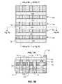
- FIGS. 2A-2Billustrate cross-sectional views of memory cells arranged in a cross-point array.
- FIGS. 3-16illustrate steps in a fabrication sequence for manufacturing the cross-point array of memory cells as illustrated in FIGS. 2A-2B .
- FIG. 17is a simplified block diagram of an integrated circuit including a cross-point memory array of fully self-aligned memory cells having diode access devices as described herein.
- FIG. 1illustrates a schematic diagram of a portion of a cross-point memory array 100 implemented using fully self-aligned pore-type memory cells having diode access devices as described herein.
- each of the memory cells of array 100includes a diode access device and a memory element (represented in FIG. 1 by a variable resistor) capable of being set to one of a plurality of resistive states and thus capable of storing one or more bits of data.
- a memory elementrepresented in FIG. 1 by a variable resistor
- the array 100comprises a plurality of word lines 130 including word lines 130 a , 130 b , and 130 c extending in parallel in a first direction, and a plurality of bit lines 120 including bit lines 120 a , 120 b , and 120 c extending in parallel in a second direction perpendicular to the first direction.
- the array 100is referred to as a cross-point array because the word lines 130 and bit lines 120 are arranged in such a manner that a given word line 130 and a given bit line 120 cross over each other but do not physically intersect, and the memory cells are located at these cross-point locations of the word lines 130 and bit lines 120 .
- Memory cell 115is representative of the memory cells of array 100 and is arranged at the cross-point location of the bit line 120 b and word line 130 b , the memory cell 115 comprising a diode 121 and memory element 160 arranged in series, the diode 121 electrically coupled to the word line 130 b and the memory element 160 electrically coupled to the bit line 120 b.
- Reading or writing to memory cell 115 of array 100can be achieved by applying appropriate voltages and/or currents to the corresponding word line 130 b and bit line 120 b to induce a current through a selected memory cell 115 .
- the level and duration of the voltages/currents appliedis dependent upon the operation performed, e.g. a reading operation or a writing operation.
- a reset pulseis applied to the corresponding word line 130 b and bit line 120 b to cause a transition of an active region of the phase change material into an amorphous phase, thereby setting the phase change material to a resistance within a resistive value range associated with the reset state.
- the reset pulseis a relatively high energy pulse, sufficient to raise the temperature of at least the active region of the memory element 160 above the transition (crystallization) temperature of the phase change material and also above the melting temperature to place at least the active region in a liquid state.
- the reset pulseis then quickly terminated, resulting in a relatively quick quenching time as the active region quickly cools to below the transition temperature so that the active region stabilizes to an amorphous phase.
- a program pulseis applied to the corresponding word line 130 b and bit line 120 b of suitable amplitude and duration to induce a current sufficient to raise the temperature of at least a portion of the active region above the transition temperature and cause a transition of a portion of the active region from the amorphous phase into a crystalline phase, this transition lowering the resistance of the memory element 160 and setting the memory cell 115 to the desired state.
- a read pulseis applied to the corresponding word line 130 b and bit line 120 b of suitable amplitude and duration to induce current to flow that does not result in the memory element 160 undergoing a change in resistive state.
- the current through the memory cell 115is dependent upon the resistance of the memory element 160 and thus the data value stored in the memory cell 115 .
- FIGS. 2A and 2Billustrate cross-sectional views of a portion of memory cells (including representative memory cell 115 ) arranged in the cross-point array 100 , FIG. 2A taken along the bit lines 120 and FIG. 2B taken along the word lines 130 .
- the memory cell 115includes a first doped semiconductor region 122 having a first conductivity type and a second doped semiconductor region 124 on the first doped semiconductor region 122 , the second doped semiconductor region 124 having a second conductivity type opposite the first conductivity type.
- the first doped semiconductor region 122 and the second doped semiconductor region 124define a pn junction 126 therebetween.
- the memory cell 115includes a conductive cap 180 on the second doped semiconductor region 124 .
- the first and second doped semiconductor regions 122 , 124 and the conductive cap 180comprise a multi-layer structure defining diode 121 .
- the conductive cap 180comprises a silicide containing, for example, Ti, W, Co, Ni, or Ta.
- the conductive cap 180assists in maintaining the uniformity of an electric field impressed across the first and second doped semiconductor regions 122 , 124 during operation by providing a contact surface that is more highly conductive than the semiconductor material of the first and second doped semiconductor regions 122 , 124 .
- the conductive cap 180can be used as a protective etch stop layer for the second doped semiconductor region 124 during the manufacturing of the memory cell 100 .
- the first doped semiconductor region 122is on word line 130 b , the word line 130 b extending into and out of the cross-section illustrated in FIG. 2A .
- the word lines 130comprise doped N + (highly doped N-type) semiconductor material
- the first doped semiconductor region 122comprises doped N ⁇ (lightly doped N-type) semiconductor material
- the second doped semiconductor region 124comprises doped P + (highly doped P-type) semiconductor material. It has been observed that the breakdown voltage of diode 121 comprising can be increased by increasing the distance between the P+ doped region and the N+ doped region and/or decreasing the doping concentration in the N ⁇ region.
- the word lines 130may comprise other conductive materials such as W, TiN, TaN, Al.
- the first doped semiconductor region 122may be omitted and the diode 121 formed from the second doped semiconductor region 124 , the conductive cap 180 and a portion of word line 130 b.
- Memory element 160is on a dielectric spacer 140 and electrically couples the diode 121 to the corresponding bit line 120 b .
- the memory element 160comprises memory material, for example, one or more materials from the group consisting of Ge, Sb, Te, Se, In, Ti, Ga, Bi, Sn, Cu, Pd, Pb, Ag, S, Si, O, P, As, N and Au.
- the memory element 160comprises a first portion 162 within an opening defined by the dielectric spacer 140 on the diode 121 to contact a top surface of the diode 121 , the first portion 262 being surrounded by the dielectric spacer 140 .
- the memory element 160also includes a second portion 164 on the first portion 162 .
- the dielectric spacer 140preferably comprises material resistive to diffusion of the memory material of memory element 160 .
- the material of dielectric spacer 140is chosen for low thermal conductivity for reasons discussed in more detail below.
- the dielectric spacer 140has sides 141 self-aligned with sides 127 of the diode 121 . In the manufacturing embodiment described in more detail below with reference to FIGS. 3-16 , material of the dielectric spacer 140 is patterned during patterning of material of the diode 121 .
- the bit lines 120extend into and out of the cross-section illustrated in FIG. 2B .
- the bit lines 120may comprise one or more layers of conductive material.
- the bit lines 120may comprise, for example, TiN or TaN.
- TiNmay be preferred in embodiments in which the memory element 160 comprises GST (discussed below) because it makes good contact with GST, it is a common material used in semiconductor manufacturing, and it provides a good diffusion barrier.
- bit lines 120may be TiAlN or TaAlN, or comprises, for further examples, one or more elements selected from the group consisting of Ti, W, Mo, Al, Ta, Cu, Pt, Ir, La, Ni, N, O, and Ru and combinations thereof.
- Dielectric 170comprising one or more layers of dielectric material, surrounds the memory cells and separates adjacent word lines 130 and adjacent bit lines 120 .
- voltages on the word line 130 b and bit line 120 bcan induce a current through the memory element 160 and the diode 121 .
- the active region 155is the region of the memory element 160 in which the memory material is induced to change between at least two solid phases. As can be appreciated, the active region 155 can be made extremely small in the illustrated structure, thus reducing the magnitude of the current needed to induce a phase change.
- the width 163 of the first portion 162 of memory element 160is less than that of the diode 121 and the second portion 164 of the memory element 160 , and preferably less than a minimum feature size for a process, typically a lithographic process, used to form the diodes 121 and word lines 130 of the memory array 100 .
- the small first portion 162 of the memory element 160concentrates current density in the first portion 162 of the memory element 160 , thereby reducing the magnitude of the current needed to induce a phase change in the active region 155 .
- the dielectric spacer 140preferably comprises material providing some thermal isolation to the active region 155 , which also helps to reduce the amount of current necessary to induce a phase change.
- the second portion 164 of the memory element 160can provide some thermal isolation from the corresponding bit line 120 for the active region 155 .
- the memory cells of the array 100are arranged at the cross-point locations of the word lines 130 and bit lines 120 .
- Memory cell 115is representative and is arranged at the cross-point location of word line 130 b and bit line 120 b .
- the diode 121 , dielectric spacer 140 , and memory element 160form a structure for memory cell 115 , the structure having a first width substantially the same as the width 134 of the word lines 130 (See FIG. 2A ).
- the structurehas a second width substantially the same as the width of the bit lines 120 (See FIG. 2B ).
- the term “substantially”is intended to accommodate manufacturing tolerances. Therefore, the cross-sectional area of the memory cells of array 100 is determined entirely by dimensions of the word lines 130 and bit lines 120 , allowing for a high memory density for array 100 .
- the word lines 130have word line widths 134 and adjacent word lines 130 are separated by a word line separation distance 132 (See FIG. 2A ), and the bit lines 120 have bit line widths 124 and adjacent bit lines 120 are separated by a bit line separation distance 125 (See FIG. 2B ).
- the summation of the word line width 134 and the word line separation distance 132is equal to twice a feature size F used to form the array 100
- the summation of the bit line width and the bit line separation distance 125is equal to twice the feature size F.
- Fis preferably a minimum feature size for a process (typically a lithographic process) used to form the bit lines 120 and word lines 130 , such that the memory cells of array 100 have a memory cell area of 4F 2 .
- the structure of memory cell 115 formed by the diode 121 , dielectric spacer 140 , and memory element 160has first and second sides 116 a , 116 b self-aligned with the sides 133 a , 133 b of the corresponding word line 130 b and has third and fourth sides 116 c , 116 d self-aligned with the sides 123 a , 123 b of the corresponding bit line 120 b .
- the diode 121is formed during the formation of the word lines 130 and the patterning of material which defines the locations of the dielectric spacer 140 , the memory element 160 and the bit lines 120 .
- the memory cells in the array 100 illustrated in the cross-sectional views of FIGS. 2A-2Bare fully self-aligned.
- FIGS. 3-16illustrate steps in a fabrication sequence for manufacturing the cross point array 100 of memory cells as illustrated in FIGS. 2A-2B .
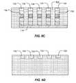
- FIGS. 3A-3Billustrate top and cross-sectional views of a first step of forming a structure 300 on a P-well.
- the multi-layer structure 300includes a word line material 310 and a diode material 312 on the word line material 310 .
- the diode material 312comprises a first doped semiconductor material layer 320 , a second doped semiconductor material layer 330 , and a conductive cap material layer 340 on the second doped semiconductor material layer 330 .
- the word line material 310comprises doped N+ (highly doped N-type) semiconductor material
- the first doped semiconductor material layer 320comprises doped N ⁇ (lightly doped N-type) semiconductor material
- the second doped semiconductor material 330comprises doped P+ (highly doped P-type) semiconductor material.
- the layers 310 , 320 , 330may be formed by implantation and activation annealing processes as known in the art.
- the conductive cap material layer 340comprises a silicide containing, for example, Ti, W, Co, Ni, or Ta.
- the layer 340comprises cobalt silicide (CoSi) and is formed by depositing a layer of cobalt and performing a rapid thermal process (RTP) such that the cobalt reacts with the silicon of layer 330 to form the layer 340 .
- RTPrapid thermal process
- other silicidesmay also be formed in this manner by depositing titanium, arsenic, doped nickel, or alloys thereof, in a manner similar to the example described herein using cobalt.
- a dielectric spacer material 350is on the diode material 312
- a sacrificial element material 360is on the dielectric spacer material 360 .
- the layers 350 , 360preferably comprise material which can be selectively processed (e.g. selectively etched) relative to one another.
- the dielectric spacer material 350comprises SiN and the sacrificial element material 360 comprises amorphous silicon.
- the layers 310 , 320 , and 330have a total thickness 315 of about 400 nm, layer 340 has a thickness 345 of about 50 nm, layer 350 has a thickness 355 of about 40 nm, and layer 360 has a thickness 365 of about 90 nm.
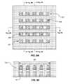
- the structure 300is patterned to form a plurality of first trenches 410 extending in a first direction to define a plurality of strips 400 , each strip 400 including word lines 130 comprising word line material of layer 310 , resulting in the structure illustrated in top and cross-sectional views of FIGS. 4A and 4B respectively.
- the word lines 130have width 134 and separation distance 132 , each preferably equal to the minimum feature size of a process, such as a lithographic process, used to form the first trenches 410 .
- the multi-layer strips 400have a pitch 420 of about 250 nm.
- the dielectric fill material 500may comprise, for example silicon dioxide, and may be formed by depositing the material 500 within the trenches 410 and then performing a planarizing process such as chemical mechanical polishing CMP.
- a sacrificial strip material 600is formed on the structure illustrated in FIGS. 5A-5B , resulting in the structure illustrated in the top and cross-sectional of FIGS. 6A and 6B respectively.
- the second sacrificial material 600comprises a layer amorphous silicon deposited having a thickness of about 90 nm.
- FIGS. 6A-6Bis patterned to form a plurality of second trenches 700 extending in parallel in a second direction to define a plurality of stacks 710 and sacrificial strips 720 comprising sacrificial strip material of layer 600 , resulting in the structure illustrated in the top view of FIG. 7A and the cross-sectional views of FIGS. 7B-7D respectively.
- the strips 720have a pitch 725 of about 250 nm.
- the trenches 700can be formed by patterning a layer of photoresist on the structure illustrated in FIGS. 6A-6B , and etching down to the word lines 130 using the patterned photoresist as an etch mask.
- each of the stacks 710includes a diode 121 comprising diode material 312 on the corresponding word line 130 , a dielectric element 730 comprising material of layer 350 on the diode 121 , and a sacrificial element 740 comprising material of layer 360 on the dielectric element 730 .
- the diodes 121include a first doped semiconductor region 122 comprising material from layer 320 , a second doped semiconductor region 124 comprising material from layer 330 , and a conductive cap 180 comprising material from layer 340 .
- the first doped semiconductor region 122 and the second doped semiconductor region 124define a pn junction 126 therebetween.
- the multi-layer stacks 710are self-aligned to the corresponding underlying word lines 130 and the corresponding overlying sacrificial strips 720 . Additionally, the stacks 710 have widths 712 , 714 and separation distances 716 , 718 both preferably equal to the minimum feature size of the process (typically a lithographic process) used to form the trenches 410 and 700 .
- the trenches 700 of the structure illustrated in FIGS. 7A-7Dare filled with additional dielectric fill material 500 , resulting in the structure illustrated in the top view of FIG. 8A and the cross-sectional views of FIGS. 8B-8D respectively.
- the trenches 700are filled with the same material as that of the dielectric 500 used to fill the trenches 410 as described above with reference to FIGS. 5A-5B .
- the dielectric fill material 500may be formed by depositing the material within the trenches 700 and then performing a planarizing process such as chemical mechanical polishing CMP to expose the top surfaces of the sacrificial strips 720 .
- the sacrificial strips 720 and the sacrificial elements 730are removed to form vias 900 at the locations of the elements 730 and trenches 920 at the locations of the strips 720 , resulting in the structure illustrated in the illustrated in the top view of FIG. 9A and the cross-sectional views of FIGS. 9B-9D .
- the sacrificial strips 720 and the sacrificial elements 730both comprise amorphous silicon and may be removed by etching using, for example, KOH or tetramethylammonium hydroxide (THMA).
- the vias 900have a height 902 of about 90 nm, and the trenches 920 have a height 922 of about 90 nm.
- sidewall spacers 1000are formed within the vias 900 of FIGS. 9A-9D , resulting in the structure illustrated in the top view of FIG. 10A and the cross-sectional views of FIGS. 10B-10D .
- the sidewall spacers 1000define openings 1010 within the vias 900 , and in the illustrated embodiment the sidewall spacers 1000 comprise silicon.
- the sidewall spacers 1000may be formed by forming a sidewall spacer material layer on the structure illustrated in FIGS. 9A-9D , and anisotropically etching the sidewall spacer material layer to expose a portion of the dielectric elements 730 .
- the openings 1010 of the sidewall spacers 1000are self-centered within the sidewall spacers 1000 .
- the sidewall spacers 1000define openings 1010 having a square-like cross-section.
- the openings 1010may have a cross-section that is circular, elliptical, rectangular or somewhat irregularly shaped, depending on the manufacturing technique applied to form the sidewall spacers 1000 .
- the dielectric elements 730are etched using the sidewall spacers 1000 as an etch mask, thereby forming dielectric spacers 140 and resulting in the structure illustrated in the top view of FIG. 11A and the cross-sectional views of FIGS. 11B-11D .
- the etchingcan be performed, for example, using Reactive Ion Etching RIE.
- the dielectric spacers 140have openings 1100 extending to the conductive caps 180 , the conductive caps 180 acting as an etch stop layer during the formation of the dielectric spacers 140 .
- the openings 1100have a width 1110 which can be sublithographic, and in the illustrated embodiment the width 1110 is about 40 nm.
- the openings 1010 of the sidewall spacers 1000can be self-centered, and thus it will be understood that the formation of the openings 1100 of the dielectric spacers 140 can also be self-centered.
- the sidewall spacers 1000are removed from the structure illustrated in FIGS. 11A-11D , resulting in the structure illustrated in the top view of FIG. 12A and cross-sectional views of FIGS. 12B-12D .
- the sidewall spacers 1000comprise silicon and may be removed by etching using, for example, KOH or THMA.
- memory elements 160are formed within the vias 900 including a first portion within the opening 1100 defined by the sidewall spacer 140 , and bit lines 120 are formed on the memory elements 160 and extend in the second direction, resulting in the structure illustrated the top view of FIG. 13A and the cross-sectional views of FIGS. 13B-13D .
- the memory elements 160 and bit lines 120may be formed by depositing a layer of phase change material on the structure illustrated in FIGS. 12A-12D , etching back the phase change material using for example Reactive Ion Etching to form elements 160 , and forming bit line material and performing a planarization process such as CMP to form the bit lines 120 .
- the memory elements 160 and bit lines 120may be formed by forming a layer of phase change material (having a thickness of about 90 nm for example) on the structure illustrated in FIGS. 12A-12D , forming a layer of bit line material (having a thickness of about 90 nm for example) on the layer of phase change material, and performing a planarizing process such as CMP.
- the diode 121was formed by the formation of the trenches 410 and 700 which also defined the word lines 130 , the sacrificial elements 730 , and the sacrificial strips 720 . Since the sacrificial elements 730 and the sacrificial strips 720 defined the locations of the subsequently formed memory elements 260 and bit lines 120 , it will be understood that the memory cells illustrated in FIG. 13A-13D are fully self-aligned.
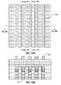
- an oxide layer 1400is formed on the structure illustrated in FIGS. 13A-13D , resulting in the structure illustrated in the top view of FIG. 14A and the cross-sectional views of FIGS. 14B-14D .
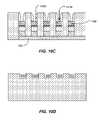
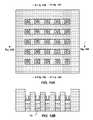
- an array of conductive plugs 1510are formed through the oxide layer 1400 to contact corresponding word lines 130 , and global word lines 1500 are formed on the oxide layer 1400 and in contact with corresponding conductive plug 1510 , resulting in the structure illustrated in FIGS. 15A-15D .
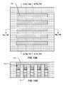
- the global word lines 1500extend to peripheral circuitry 1600 including CMOS devices as shown in the top view of FIG. 16A and the cross-sectional views of FIG. 16B .
- FIG. 17is a simplified block diagram of an integrated circuit 10 including a cross-point memory array 100 of fully self-aligned memory cells having diode access devices as described herein.
- a word line decoder 14is coupled to and in electrical communication with a plurality of word lines 16 .
- a bit line (column) decoder 18is in electrical communication with a plurality of bit lines 20 to read data from, and write data to, the phase change memory cells (not shown) in array 100 . Addresses are supplied on bus 22 to word line decoder and drivers 14 and bit line decoder 18 .
- Sense amplifiers and data-in structures in block 24are coupled to bit line decoder 18 via data bus 26 .
- Datais supplied via a data-in line 28 from input/output ports on integrated circuit 10 , or from other data sources internal or external to integrated circuit 10 , to data-in structures in block 24 .
- Other circuitry 30may be included on integrated circuit 10 , such as a general purpose processor or special purpose application circuitry, or a combination of modules providing system-on-a-chip functionality supported by array 100 .
- Datais supplied via a data-out line 32 from the sense amplifiers in block 24 to input/output ports on integrated circuit 10 , or to other data destinations internal or external to integrated circuit 10 .
- Controller 34may be implemented using special-purpose logic circuitry as known in the art.
- controller 34comprises a general-purpose processor, which may be implemented on the same integrated circuit to execute a computer program to control the operations of the device.
- a combination of special-purpose logic circuitry and a general-purpose processormay be utilized for implementation of controller 34 .
- Embodiments of the memory cells described hereininclude phase change based memory materials, including chalcogenide based materials and other materials, for the memory element.
- Chalcogensinclude any of the four elements oxygen (O), sulfur (S), selenium (Se), and tellurium (Te), forming part of group VIA of the periodic table.
- Chalcogenidescomprise compounds of a chalcogen with a more electropositive element or radical.
- Chalcogenide alloyscomprise combinations of chalcogenides with other materials such as transition metals.
- a chalcogenide alloyusually contains one or more elements from group IVA of the periodic table of elements, such as germanium (Ge) and tin (Sn).
- chalcogenide alloysinclude combinations including one or more of antimony (Sb), gallium (Ga), indium (In), and silver (Ag).
- Sbantimony
- Gagallium
- Inindium
- silversilver
- phase change based memory materialsinclude alloys of: Ga/Sb, In/Sb, In/Se, Sb/Te, Ge/Te, Ge/Sb/Te, In/Sb/Te, Ga/Se/Te, Sn/Sb/Te, In/Sb/Ge, Ag/In/Sb/Te, Ge/Sn/Sb/Te, Ge/Sb/Se/Te and Te/Ge/Sb/S.
- compositionscan be workable.
- the compositionscan be characterized as Te a Ge b Sb 100 ⁇ (a+b) .
- One researcherhas described the most useful alloys as having an average concentration of Te in the deposited materials well below 70%, typically below about 60% and ranged in general from as low as about 23% up to about 58% Te and most preferably about 48% to 58% Te.
- Concentrations of Gewere above about 5% and ranged from a low of about 8% to about 30% average in the material, remaining generally below 50%. Most preferably, concentrations of Ge ranged from about 8% to about 40%. The remainder of the principal constituent elements in this composition was Sb.
- a transition metalsuch as chromium (Cr), iron (Fe), nickel (Ni), niobium (Nb), palladium (Pd), platinum (Pt) and mixtures or alloys thereof may be combined with Ge/Sb/Te to form a phase change alloy that has programmable resistive properties.
- chromium (Cr)iron (Fe), nickel (Ni), niobium (Nb), palladium (Pd), platinum (Pt) and mixtures or alloys thereof
- Ge/Sb/Techromium
- Specific examples of memory materials that may be usefulare given in Ovshinsky '112 at columns 11-13, which examples are hereby incorporated by reference.
- Chalcogenides and other phase change materialsare doped with impurities in some embodiments to modify conductivity, transition temperature, melting temperature, and other properties of memory elements using the doped chalcogenides.
- Representative impurities used for doping chalcogenidesinclude nitrogen, silicon, oxygen, silicon dioxide, silicon nitride, copper, silver, gold, aluminum, aluminum oxide, tantalum, tantalum oxide, tantalum nitride, titanium and titanium oxide. See, e.g., U.S. Pat. No. 6,800,504, and U.S. Patent Application Publication No. U.S. 2005/0029502.
- Phase change alloysare capable of being switched between a first structural state in which the material is in a generally amorphous solid phase, and a second structural state in which the material is in a generally crystalline solid phase in its local order in the active channel region of the cell. These alloys are at least bistable.
- amorphousis used to refer to a relatively less ordered structure, more disordered than a single crystal, which has the detectable characteristics such as higher electrical resistivity than the crystalline phase.
- crystallineis used to refer to a relatively more ordered structure, more ordered than in an amorphous structure, which has detectable characteristics such as lower electrical resistivity than the amorphous phase.
- phase change materialsmay be electrically switched between different detectable states of local order across the spectrum between completely amorphous and completely crystalline states.
- Other material characteristics affected by the change between amorphous and crystalline phasesinclude atomic order, free electron density and activation energy.
- the materialmay be switched either into different solid phases or into mixtures of two or more solid phases, providing a gray scale between completely amorphous and completely crystalline states.
- the electrical properties in the materialmay vary accordingly.
- Phase change alloyscan be changed from one phase state to another by application of electrical pulses. It has been observed that a shorter, higher amplitude pulse tends to change the phase change material to a generally amorphous state. A longer, lower amplitude pulse tends to change the phase change material to a generally crystalline state. The energy in a shorter, higher amplitude pulse is high enough to allow for bonds of the crystalline structure to be broken and short enough to prevent the atoms from realigning into a crystalline state. Appropriate profiles for pulses can be determined, without undue experimentation, specifically adapted to a particular phase change alloy. In following sections of the disclosure, the phase change material is referred to as GST, and it will be understood that other types of phase change materials can be used. A material useful for implementation of a PCRAM described herein is Ge 2 Sb 2 Te 5 .
- programmable resistive memory materialsmay be used in other embodiments of the invention, including N 2 doped GST, GexSby, or other material that uses different crystal phase changes to determine resistance; Pr x Ca y MnO 3 , Pr x Sr y MnO 3 , ZrO x , or other material that uses an electrical pulse to change the resistance state; 7,7,8,8-tetracyanoquinodimethane (TCNQ), methanofullerene 6,6-phenyl C61-butyric acid methyl ester (PCBM), TCNQ-PCBM, Cu-TCNQ, Ag-TCNQ, C60-TCNQ, TCNQ doped with other metal, or any other polymer material that has a bistable or multi-stable resistance state controlled by an electrical pulse.
- TCNQ7,7,8,8-tetracyanoquinodimethane
- PCBMmethanofullerene 6,6-phenyl C61-butyric acid methyl ester
- An exemplary method for forming chalcogenide materialuses PVD-sputtering or magnetron-sputtering method with source gas(es) of Ar, N2, and/or He, etc. at the pressure of 1 mTorr ⁇ 100 mTorr.
- the depositionis usually done at room temperature.
- a collimator with an aspect ratio of 1 ⁇ 5can be used to improve the fill-in performance.
- a DC bias of several tens of volts to several hundreds of voltsis also used.
- the combination of DC bias and the collimatercan be used simultaneously.
- a post-deposition annealing treatment in a vacuum or in an N 2 ambientis optionally performed to improve the crystallize state of chalcogenide material.
- the annealing temperaturetypically ranges from 100° C. to 400° C. with an anneal time of less than 30 minutes.
- chalcogenide materialdepends on the design of cell structure.
- a chalcogenide material with thickness of higher than 8 nmcan have a phase change characterization so that the material exhibits at least two stable resistance states.
Landscapes
- Engineering & Computer Science (AREA)
- Manufacturing & Machinery (AREA)
- Chemical & Material Sciences (AREA)
- Materials Engineering (AREA)
- Semiconductor Memories (AREA)
Abstract
Description
Claims (22)
Priority Applications (3)
| Application Number | Priority Date | Filing Date | Title |
|---|---|---|---|
| US12/177,533US7932506B2 (en) | 2008-07-22 | 2008-07-22 | Fully self-aligned pore-type memory cell having diode access device |
| TW097128677ATWI387103B (en) | 2008-07-22 | 2008-07-29 | Fully self-aligned pore-type memory cell having diode access device |
| CN2009101597998ACN101685827B (en) | 2008-07-22 | 2009-07-22 | A storage device and its manufacturing method |
Applications Claiming Priority (1)
| Application Number | Priority Date | Filing Date | Title |
|---|---|---|---|
| US12/177,533US7932506B2 (en) | 2008-07-22 | 2008-07-22 | Fully self-aligned pore-type memory cell having diode access device |
Publications (2)
| Publication Number | Publication Date |
|---|---|
| US20100019221A1 US20100019221A1 (en) | 2010-01-28 |
| US7932506B2true US7932506B2 (en) | 2011-04-26 |
Family
ID=41567821
Family Applications (1)
| Application Number | Title | Priority Date | Filing Date |
|---|---|---|---|
| US12/177,533Active2029-05-04US7932506B2 (en) | 2008-07-22 | 2008-07-22 | Fully self-aligned pore-type memory cell having diode access device |
Country Status (3)
| Country | Link |
|---|---|
| US (1) | US7932506B2 (en) |
| CN (1) | CN101685827B (en) |
| TW (1) | TWI387103B (en) |
Cited By (4)
| Publication number | Priority date | Publication date | Assignee | Title |
|---|---|---|---|---|
| US20100078619A1 (en)* | 2008-09-30 | 2010-04-01 | Stmicroelectronics S.R.L. | Resistive memory cell and method for manufacturing a resistive memory cell |
| US20100112774A1 (en)* | 2008-10-30 | 2010-05-06 | Gyuhwan Oh | Variable Resistance Memory Device and Methods of Forming the Same |
| US20140231742A1 (en)* | 2013-02-21 | 2014-08-21 | Winbond Electronics Corp. | Resistance memory device |
| US9256126B2 (en) | 2012-11-14 | 2016-02-09 | Irresistible Materials Ltd | Methanofullerenes |
Families Citing this family (76)
| Publication number | Priority date | Publication date | Assignee | Title |
|---|---|---|---|---|
| US9178141B2 (en) | 2006-04-04 | 2015-11-03 | Micron Technology, Inc. | Memory elements using self-aligned phase change material layers and methods of manufacturing same |
| WO2010076827A1 (en)* | 2008-12-30 | 2010-07-08 | Fabio Pellizzer | Method for fabricating a phase-change memory cell |
| US8431492B2 (en)* | 2010-02-02 | 2013-04-30 | Sandisk 3D Llc | Memory cell that includes a sidewall collar for pillar isolation and methods of forming the same |
| US9601692B1 (en) | 2010-07-13 | 2017-03-21 | Crossbar, Inc. | Hetero-switching layer in a RRAM device and method |
| US9012307B2 (en) | 2010-07-13 | 2015-04-21 | Crossbar, Inc. | Two terminal resistive switching device structure and method of fabricating |
| US8946046B1 (en) | 2012-05-02 | 2015-02-03 | Crossbar, Inc. | Guided path for forming a conductive filament in RRAM |
| US9570678B1 (en) | 2010-06-08 | 2017-02-14 | Crossbar, Inc. | Resistive RAM with preferental filament formation region and methods |
| CN103081093B (en) | 2010-06-11 | 2015-06-03 | 科洛斯巴股份有限公司 | Pillar structure and method of memory device |
| US8310864B2 (en) | 2010-06-15 | 2012-11-13 | Macronix International Co., Ltd. | Self-aligned bit line under word line memory array |
| US8374018B2 (en) | 2010-07-09 | 2013-02-12 | Crossbar, Inc. | Resistive memory using SiGe material |
| US8395140B2 (en) | 2010-07-09 | 2013-03-12 | Micron Technology, Inc. | Cross-point memory utilizing Ru/Si diode |
| US8884261B2 (en) | 2010-08-23 | 2014-11-11 | Crossbar, Inc. | Device switching using layered device structure |
| US8168506B2 (en) | 2010-07-13 | 2012-05-01 | Crossbar, Inc. | On/off ratio for non-volatile memory device and method |
| US8467227B1 (en) | 2010-11-04 | 2013-06-18 | Crossbar, Inc. | Hetero resistive switching material layer in RRAM device and method |
| US8569172B1 (en) | 2012-08-14 | 2013-10-29 | Crossbar, Inc. | Noble metal/non-noble metal electrode for RRAM applications |
| US8947908B2 (en) | 2010-11-04 | 2015-02-03 | Crossbar, Inc. | Hetero-switching layer in a RRAM device and method |
| US8492195B2 (en) | 2010-08-23 | 2013-07-23 | Crossbar, Inc. | Method for forming stackable non-volatile resistive switching memory devices |
| US9401475B1 (en) | 2010-08-23 | 2016-07-26 | Crossbar, Inc. | Method for silver deposition for a non-volatile memory device |
| US8404553B2 (en) | 2010-08-23 | 2013-03-26 | Crossbar, Inc. | Disturb-resistant non-volatile memory device and method |
| US8889521B1 (en) | 2012-09-14 | 2014-11-18 | Crossbar, Inc. | Method for silver deposition for a non-volatile memory device |
| US8391049B2 (en) | 2010-09-29 | 2013-03-05 | Crossbar, Inc. | Resistor structure for a non-volatile memory device and method |
| US8558212B2 (en) | 2010-09-29 | 2013-10-15 | Crossbar, Inc. | Conductive path in switching material in a resistive random access memory device and control |
| US8502185B2 (en) | 2011-05-31 | 2013-08-06 | Crossbar, Inc. | Switching device having a non-linear element |
| USRE46335E1 (en) | 2010-11-04 | 2017-03-07 | Crossbar, Inc. | Switching device having a non-linear element |
| US8930174B2 (en) | 2010-12-28 | 2015-01-06 | Crossbar, Inc. | Modeling technique for resistive random access memory (RRAM) cells |
| US8815696B1 (en) | 2010-12-31 | 2014-08-26 | Crossbar, Inc. | Disturb-resistant non-volatile memory device using via-fill and etchback technique |
| US9153623B1 (en) | 2010-12-31 | 2015-10-06 | Crossbar, Inc. | Thin film transistor steering element for a non-volatile memory device |
| US8791010B1 (en) | 2010-12-31 | 2014-07-29 | Crossbar, Inc. | Silver interconnects for stacked non-volatile memory device and method |
| KR20120104031A (en)* | 2011-03-11 | 2012-09-20 | 삼성전자주식회사 | Phase change material layer, method of forming a phase change layer, phase change memory device and method of manufacturing a phase change memory device |
| US8486743B2 (en) | 2011-03-23 | 2013-07-16 | Micron Technology, Inc. | Methods of forming memory cells |
| US9620206B2 (en) | 2011-05-31 | 2017-04-11 | Crossbar, Inc. | Memory array architecture with two-terminal memory cells |
| US8619459B1 (en) | 2011-06-23 | 2013-12-31 | Crossbar, Inc. | High operating speed resistive random access memory |
| US9564587B1 (en) | 2011-06-30 | 2017-02-07 | Crossbar, Inc. | Three-dimensional two-terminal memory with enhanced electric field and segmented interconnects |
| US9627443B2 (en) | 2011-06-30 | 2017-04-18 | Crossbar, Inc. | Three-dimensional oblique two-terminal memory with enhanced electric field |
| US8946669B1 (en) | 2012-04-05 | 2015-02-03 | Crossbar, Inc. | Resistive memory device and fabrication methods |
| US9166163B2 (en) | 2011-06-30 | 2015-10-20 | Crossbar, Inc. | Sub-oxide interface layer for two-terminal memory |
| US8659929B2 (en) | 2011-06-30 | 2014-02-25 | Crossbar, Inc. | Amorphous silicon RRAM with non-linear device and operation |
| US9252191B2 (en) | 2011-07-22 | 2016-02-02 | Crossbar, Inc. | Seed layer for a p+ silicon germanium material for a non-volatile memory device and method |
| US10056907B1 (en) | 2011-07-29 | 2018-08-21 | Crossbar, Inc. | Field programmable gate array utilizing two-terminal non-volatile memory |
| US9729155B2 (en) | 2011-07-29 | 2017-08-08 | Crossbar, Inc. | Field programmable gate array utilizing two-terminal non-volatile memory |
| US8674724B2 (en) | 2011-07-29 | 2014-03-18 | Crossbar, Inc. | Field programmable gate array utilizing two-terminal non-volatile memory |
| JP5611903B2 (en)* | 2011-08-09 | 2014-10-22 | 株式会社東芝 | Resistance change memory |
| US8994489B2 (en) | 2011-10-19 | 2015-03-31 | Micron Technology, Inc. | Fuses, and methods of forming and using fuses |
| US8723155B2 (en) | 2011-11-17 | 2014-05-13 | Micron Technology, Inc. | Memory cells and integrated devices |
| US9252188B2 (en)* | 2011-11-17 | 2016-02-02 | Micron Technology, Inc. | Methods of forming memory cells |
| US8716098B1 (en) | 2012-03-09 | 2014-05-06 | Crossbar, Inc. | Selective removal method and structure of silver in resistive switching device for a non-volatile memory device |
| US9087576B1 (en) | 2012-03-29 | 2015-07-21 | Crossbar, Inc. | Low temperature fabrication method for a three-dimensional memory device and structure |
| US9685608B2 (en) | 2012-04-13 | 2017-06-20 | Crossbar, Inc. | Reduced diffusion in metal electrode for two-terminal memory |
| US8658476B1 (en) | 2012-04-20 | 2014-02-25 | Crossbar, Inc. | Low temperature P+ polycrystalline silicon material for non-volatile memory device |
| US9136467B2 (en) | 2012-04-30 | 2015-09-15 | Micron Technology, Inc. | Phase change memory cells and methods of forming phase change memory cells |
| US8765555B2 (en) | 2012-04-30 | 2014-07-01 | Micron Technology, Inc. | Phase change memory cells and methods of forming phase change memory cells |
| US8796658B1 (en) | 2012-05-07 | 2014-08-05 | Crossbar, Inc. | Filamentary based non-volatile resistive memory device and method |
| US8765566B2 (en) | 2012-05-10 | 2014-07-01 | Crossbar, Inc. | Line and space architecture for a non-volatile memory device |
| US8877628B2 (en) | 2012-07-12 | 2014-11-04 | Micron Technologies, Inc. | Methods of forming nano-scale pores, nano-scale electrical contacts, and memory devices including nano-scale electrical contacts, and related structures and devices |
| US9583701B1 (en) | 2012-08-14 | 2017-02-28 | Crossbar, Inc. | Methods for fabricating resistive memory device switching material using ion implantation |
| US9741765B1 (en) | 2012-08-14 | 2017-08-22 | Crossbar, Inc. | Monolithically integrated resistive memory using integrated-circuit foundry compatible processes |
| US8946673B1 (en) | 2012-08-24 | 2015-02-03 | Crossbar, Inc. | Resistive switching device structure with improved data retention for non-volatile memory device and method |
| US9312483B2 (en) | 2012-09-24 | 2016-04-12 | Crossbar, Inc. | Electrode structure for a non-volatile memory device and method |
| US9576616B2 (en) | 2012-10-10 | 2017-02-21 | Crossbar, Inc. | Non-volatile memory with overwrite capability and low write amplification |
| US11068620B2 (en) | 2012-11-09 | 2021-07-20 | Crossbar, Inc. | Secure circuit integrated with memory layer |
| US8982647B2 (en) | 2012-11-14 | 2015-03-17 | Crossbar, Inc. | Resistive random access memory equalization and sensing |
| US9412790B1 (en) | 2012-12-04 | 2016-08-09 | Crossbar, Inc. | Scalable RRAM device architecture for a non-volatile memory device and method |
| US9406379B2 (en) | 2013-01-03 | 2016-08-02 | Crossbar, Inc. | Resistive random access memory with non-linear current-voltage relationship |
| US9324942B1 (en) | 2013-01-31 | 2016-04-26 | Crossbar, Inc. | Resistive memory cell with solid state diode |
| US9112145B1 (en) | 2013-01-31 | 2015-08-18 | Crossbar, Inc. | Rectified switching of two-terminal memory via real time filament formation |
| US8934280B1 (en) | 2013-02-06 | 2015-01-13 | Crossbar, Inc. | Capacitive discharge programming for two-terminal memory cells |
| US9553262B2 (en) | 2013-02-07 | 2017-01-24 | Micron Technology, Inc. | Arrays of memory cells and methods of forming an array of memory cells |
| US9093635B2 (en) | 2013-03-14 | 2015-07-28 | Crossbar, Inc. | Controlling on-state current for two-terminal memory |
| US9691981B2 (en)* | 2013-05-22 | 2017-06-27 | Micron Technology, Inc. | Memory cell structures |
| US10290801B2 (en) | 2014-02-07 | 2019-05-14 | Crossbar, Inc. | Scalable silicon based resistive memory device |
| US9881971B2 (en) | 2014-04-01 | 2018-01-30 | Micron Technology, Inc. | Memory arrays |
| US9362494B2 (en) | 2014-06-02 | 2016-06-07 | Micron Technology, Inc. | Array of cross point memory cells and methods of forming an array of cross point memory cells |
| US9343506B2 (en) | 2014-06-04 | 2016-05-17 | Micron Technology, Inc. | Memory arrays with polygonal memory cells having specific sidewall orientations |
| KR102446863B1 (en)* | 2016-02-22 | 2022-09-23 | 삼성전자주식회사 | Memory device and method for manufacturing the same |
| US10580976B2 (en)* | 2018-03-19 | 2020-03-03 | Sandisk Technologies Llc | Three-dimensional phase change memory device having a laterally constricted element and method of making the same |
| US11417841B2 (en)* | 2019-08-13 | 2022-08-16 | Micron Technology, Inc. | Techniques for forming self-aligned memory structures |
Citations (274)
| Publication number | Priority date | Publication date | Assignee | Title |
|---|---|---|---|---|
| US3271591A (en) | 1963-09-20 | 1966-09-06 | Energy Conversion Devices Inc | Symmetrical current controlling device |
| US3530441A (en) | 1969-01-15 | 1970-09-22 | Energy Conversion Devices Inc | Method and apparatus for storing and retrieving information |
| US4452592A (en) | 1982-06-01 | 1984-06-05 | General Motors Corporation | Cyclic phase change coupling |
| US4599705A (en) | 1979-12-13 | 1986-07-08 | Energy Conversion Devices, Inc. | Programmable cell for use in programmable electronic arrays |
| US4719594A (en) | 1984-11-01 | 1988-01-12 | Energy Conversion Devices, Inc. | Grooved optical data storage device including a chalcogenide memory layer |
| US4769339A (en) | 1983-12-26 | 1988-09-06 | Kabushiki Kaisha Toshiba | Method of manufacturing a field effect transistor device having a multilayer gate electrode |
| US4876220A (en) | 1986-05-16 | 1989-10-24 | Actel Corporation | Method of making programmable low impedance interconnect diode element |
| US4959812A (en) | 1987-12-28 | 1990-09-25 | Kabushiki Kaisha Toshiba | Electrically erasable programmable read-only memory with NAND cell structure |
| US5106775A (en) | 1987-12-10 | 1992-04-21 | Hitachi, Ltd. | Process for manufacturing vertical dynamic random access memories |
| US5166096A (en) | 1991-10-29 | 1992-11-24 | International Business Machines Corporation | Process for fabricating self-aligned contact studs for semiconductor structures |
| US5166758A (en) | 1991-01-18 | 1992-11-24 | Energy Conversion Devices, Inc. | Electrically erasable phase change memory |
| US5177567A (en) | 1991-07-19 | 1993-01-05 | Energy Conversion Devices, Inc. | Thin-film structure for chalcogenide electrical switching devices and process therefor |
| US5332923A (en) | 1991-08-06 | 1994-07-26 | Nec Corporation | Semiconductor memory |
| US5391901A (en) | 1992-10-30 | 1995-02-21 | Nec Corporation | Semiconductor memory with oblique folded bit-line arrangement |
| US5515488A (en) | 1994-08-30 | 1996-05-07 | Xerox Corporation | Method and apparatus for concurrent graphical visualization of a database search and its search history |
| US5534712A (en) | 1991-01-18 | 1996-07-09 | Energy Conversion Devices, Inc. | Electrically erasable memory elements characterized by reduced current and improved thermal stability |
| US5550396A (en) | 1992-01-24 | 1996-08-27 | Mitsubishi Denki Kabushiki Kaisha | Vertical field effect transistor with a trench structure |
| US5687112A (en) | 1996-04-19 | 1997-11-11 | Energy Conversion Devices, Inc. | Multibit single cell memory element having tapered contact |
| US5688713A (en) | 1996-08-26 | 1997-11-18 | Vanguard International Semiconductor Corporation | Method of manufacturing a DRAM cell having a double-crown capacitor using polysilicon and nitride spacers |
| US5716883A (en) | 1996-11-06 | 1998-02-10 | Vanguard International Semiconductor Corporation | Method of making increased surface area, storage node electrode, with narrow spaces between polysilicon columns |
| US5754472A (en) | 1995-12-27 | 1998-05-19 | Hyundai Electronics Industries Co., Ltd. | Flash memory device having a program path the same as a read pre-condition path |
| US5789758A (en) | 1995-06-07 | 1998-08-04 | Micron Technology, Inc. | Chalcogenide memory cell with a plurality of chalcogenide electrodes |
| US5789277A (en) | 1996-07-22 | 1998-08-04 | Micron Technology, Inc. | Method of making chalogenide memory device |
| US5814527A (en) | 1996-07-22 | 1998-09-29 | Micron Technology, Inc. | Method of making small pores defined by a disposable internal spacer for use in chalcogenide memories |
| US5831276A (en) | 1995-06-07 | 1998-11-03 | Micron Technology, Inc. | Three-dimensional container diode for use with multi-state material in a non-volatile memory cell |
| US5837564A (en) | 1995-11-01 | 1998-11-17 | Micron Technology, Inc. | Method for optimal crystallization to obtain high electrical performance from chalcogenides |
| US5869843A (en) | 1995-06-07 | 1999-02-09 | Micron Technology, Inc. | Memory array having a multi-state element and method for forming such array or cells thereof |
| US5879955A (en) | 1995-06-07 | 1999-03-09 | Micron Technology, Inc. | Method for fabricating an array of ultra-small pores for chalcogenide memory cells |
| US5902704A (en) | 1997-07-02 | 1999-05-11 | Lsi Logic Corporation | Process for forming photoresist mask over integrated circuit structures with critical dimension control |
| US5933365A (en) | 1997-06-19 | 1999-08-03 | Energy Conversion Devices, Inc. | Memory element with energy control mechanism |
| US5952671A (en) | 1997-05-09 | 1999-09-14 | Micron Technology, Inc. | Small electrode for a chalcogenide switching device and method for fabricating same |
| US5958358A (en) | 1992-07-08 | 1999-09-28 | Yeda Research And Development Co., Ltd. | Oriented polycrystalline thin films of transition metal chalcogenides |
| US5970336A (en) | 1996-08-22 | 1999-10-19 | Micron Technology, Inc. | Method of making memory cell incorporating a chalcogenide element |
| US5985698A (en) | 1996-07-22 | 1999-11-16 | Micron Technology, Inc. | Fabrication of three dimensional container diode for use with multi-state material in a non-volatile memory cell |
| US6011725A (en) | 1997-08-01 | 2000-01-04 | Saifun Semiconductors, Ltd. | Two bit non-volatile electrically erasable and programmable semiconductor memory cell utilizing asymmetrical charge trapping |
| US6025220A (en) | 1996-06-18 | 2000-02-15 | Micron Technology, Inc. | Method of forming a polysilicon diode and devices incorporating such diode |
| US6031287A (en) | 1997-06-18 | 2000-02-29 | Micron Technology, Inc. | Contact structure and memory element incorporating the same |
| US6034882A (en) | 1998-11-16 | 2000-03-07 | Matrix Semiconductor, Inc. | Vertically stacked field programmable nonvolatile memory and method of fabrication |
| US6046951A (en) | 1998-01-23 | 2000-04-04 | Stmicroelectronics S.A. | Process for controlling the read circuit of a memory plane and corresponding memory device |
| US6066870A (en) | 1996-07-16 | 2000-05-23 | Micron Technology, Inc. | Single digit line with cell contact interconnect |
| US6077674A (en) | 1999-10-27 | 2000-06-20 | Agilent Technologies Inc. | Method of producing oligonucleotide arrays with features of high purity |
| US6087269A (en) | 1998-04-20 | 2000-07-11 | Advanced Micro Devices, Inc. | Method of making an interconnect using a tungsten hard mask |
| US6087674A (en) | 1996-10-28 | 2000-07-11 | Energy Conversion Devices, Inc. | Memory element with memory material comprising phase-change material and dielectric material |
| US6114713A (en) | 1997-01-28 | 2000-09-05 | Zahorik; Russell C. | Integrated circuit memory cell having a small active area and method of forming same |
| US6117720A (en) | 1995-06-07 | 2000-09-12 | Micron Technology, Inc. | Method of making an integrated circuit electrode having a reduced contact area |
| US6147395A (en) | 1996-10-02 | 2000-11-14 | Micron Technology, Inc. | Method for fabricating a small area of contact between electrodes |
| US6177317B1 (en) | 1999-04-14 | 2001-01-23 | Macronix International Co., Ltd. | Method of making nonvolatile memory devices having reduced resistance diffusion regions |
| US6271090B1 (en) | 2000-12-22 | 2001-08-07 | Macronix International Co., Ltd. | Method for manufacturing flash memory device with dual floating gates and two bits per cell |
| US6280684B1 (en) | 1994-12-13 | 2001-08-28 | Ricoh Company, Ltd. | Sputtering target, method of producing the target, optical recording medium fabricated by using the sputtering target, and method of fabricating the optical recording medium |
| US6291137B1 (en) | 1999-01-20 | 2001-09-18 | Advanced Micro Devices, Inc. | Sidewall formation for sidewall patterning of sub 100 nm structures |
| US6314014B1 (en) | 1999-12-16 | 2001-11-06 | Ovonyx, Inc. | Programmable resistance memory arrays with reference cells |
| US6316348B1 (en) | 1999-02-05 | 2001-11-13 | Taiwan Semiconductor Manufacturing Company | High selectivity Si-rich SiON etch-stop layer |
| US6320786B1 (en) | 2000-12-22 | 2001-11-20 | Macronix International Co., Ltd. | Method of controlling multi-state NROM |
| US6326307B1 (en) | 1999-11-15 | 2001-12-04 | Appllied Materials, Inc. | Plasma pretreatment of photoresist in an oxide etch process |
| US6339544B1 (en) | 2000-09-29 | 2002-01-15 | Intel Corporation | Method to enhance performance of thermal resistor device |
| US6351406B1 (en) | 1998-11-16 | 2002-02-26 | Matrix Semiconductor, Inc. | Vertically stacked field programmable nonvolatile memory and method of fabrication |
| US6372651B1 (en) | 1998-07-17 | 2002-04-16 | Advanced Micro Devices, Inc. | Method for trimming a photoresist pattern line for memory gate etching |
| US6380068B2 (en) | 2000-01-05 | 2002-04-30 | Macronix International Co., Ltd. | Method for planarizing a flash memory device |
| US20020070457A1 (en) | 2000-12-09 | 2002-06-13 | Samsung Electronics Co., Ltd. | Metal contact structure in semiconductor device and method for forming the same |
| US6420215B1 (en) | 2000-04-28 | 2002-07-16 | Matrix Semiconductor, Inc. | Three-dimensional memory array and method of fabrication |
| US6420216B1 (en) | 2000-03-14 | 2002-07-16 | International Business Machines Corporation | Fuse processing using dielectric planarization pillars |
| US6429064B1 (en) | 2000-09-29 | 2002-08-06 | Intel Corporation | Reduced contact area of sidewall conductor |
| US20020113273A1 (en) | 2001-02-22 | 2002-08-22 | Samsung Electronics Co., Ltd. | Semiconductor device having contact plug and method for manufacturing the same |
| US6440837B1 (en) | 2000-07-14 | 2002-08-27 | Micron Technology, Inc. | Method of forming a contact structure in a semiconductor device |
| US6483736B2 (en) | 1998-11-16 | 2002-11-19 | Matrix Semiconductor, Inc. | Vertically stacked field programmable nonvolatile memory and method of fabrication |
| US6487114B2 (en) | 2001-02-28 | 2002-11-26 | Macronix International Co., Ltd. | Method of reading two-bit memories of NROM cell |
| US6487106B1 (en) | 1999-01-12 | 2002-11-26 | Arizona Board Of Regents | Programmable microelectronic devices and method of forming and programming same |
| US6501111B1 (en) | 2000-06-30 | 2002-12-31 | Intel Corporation | Three-dimensional (3D) programmable device |
| US6511867B2 (en) | 2001-06-30 | 2003-01-28 | Ovonyx, Inc. | Utilizing atomic layer deposition for programmable device |
| US6512241B1 (en) | 2001-12-31 | 2003-01-28 | Intel Corporation | Phase change material memory device |
| US6514788B2 (en) | 2001-05-29 | 2003-02-04 | Bae Systems Information And Electronic Systems Integration Inc. | Method for manufacturing contacts for a Chalcogenide memory device |
| US6514820B2 (en) | 1998-08-27 | 2003-02-04 | Micron Technology, Inc. | Method for forming single electron resistor memory |
| US6534781B2 (en) | 2000-12-26 | 2003-03-18 | Ovonyx, Inc. | Phase-change memory bipolar array utilizing a single shallow trench isolation for creating an individual active area region for two memory array elements and one bipolar base contact |
| US6545903B1 (en) | 2001-12-17 | 2003-04-08 | Texas Instruments Incorporated | Self-aligned resistive plugs for forming memory cell with phase change material |
| US20030072195A1 (en) | 2001-06-12 | 2003-04-17 | Thomas Mikolajick | Semiconductor memory device and fabrication method |
| US6551866B1 (en) | 1998-11-27 | 2003-04-22 | Mitsubishi Denki Kabushiki Kaisha | Method of manufacturing a semiconductor memory device |
| US6555860B2 (en) | 2000-09-29 | 2003-04-29 | Intel Corporation | Compositionally modified resistive electrode |
| US6563156B2 (en) | 2001-03-15 | 2003-05-13 | Micron Technology, Inc. | Memory elements and methods for making same |
| US6566700B2 (en) | 2001-10-11 | 2003-05-20 | Ovonyx, Inc. | Carbon-containing interfacial layer for phase-change memory |
| US6567293B1 (en) | 2000-09-29 | 2003-05-20 | Ovonyx, Inc. | Single level metal memory cell using chalcogenide cladding |
| US20030095426A1 (en) | 2001-11-20 | 2003-05-22 | Glen Hush | Complementary bit PCRAM sense amplifier and method of operation |
| US6576546B2 (en) | 1999-12-22 | 2003-06-10 | Texas Instruments Incorporated | Method of enhancing adhesion of a conductive barrier layer to an underlying conductive plug and contact for ferroelectric applications |
| US6579760B1 (en) | 2002-03-28 | 2003-06-17 | Macronix International Co., Ltd. | Self-aligned, programmable phase change memory |
| US6586761B2 (en) | 2001-09-07 | 2003-07-01 | Intel Corporation | Phase change material memory device |
| US6589714B2 (en) | 2001-06-26 | 2003-07-08 | Ovonyx, Inc. | Method for making programmable resistance memory element using silylated photoresist |
| US6596589B2 (en) | 2001-04-30 | 2003-07-22 | Vanguard International Semiconductor Corporation | Method of manufacturing a high coupling ratio stacked gate flash memory with an HSG-SI layer |
| US6605527B2 (en) | 2001-06-30 | 2003-08-12 | Intel Corporation | Reduced area intersection between electrode and programming element |
| US6605821B1 (en) | 2002-05-10 | 2003-08-12 | Hewlett-Packard Development Company, L.P. | Phase change material electronic memory structure and method for forming |
| US6613604B2 (en) | 2001-08-02 | 2003-09-02 | Ovonyx, Inc. | Method for making small pore for use in programmable resistance memory element |
| US6617192B1 (en) | 1997-10-01 | 2003-09-09 | Ovonyx, Inc. | Electrically programmable memory element with multi-regioned contact |
| US6627530B2 (en) | 2000-12-22 | 2003-09-30 | Matrix Semiconductor, Inc. | Patterning three dimensional structures |
| US6639849B2 (en) | 2002-02-28 | 2003-10-28 | Fujitsu Limited | Nonvolatile semiconductor memory device programming second dynamic reference cell according to threshold value of first dynamic reference cell |
| US6673700B2 (en) | 2001-06-30 | 2004-01-06 | Ovonyx, Inc. | Reduced area intersection between electrode and programming element |
| US6674115B2 (en) | 2001-08-31 | 2004-01-06 | Intel Corporation | Multiple layer phrase-change memory |
| US6677678B2 (en) | 2000-03-14 | 2004-01-13 | International Business Machines Corporation | Damascene structure using a sacrificial conductive layer |
| US20040026686A1 (en) | 2002-08-09 | 2004-02-12 | Macronix International Co., Ltd. | Spacer chalcogenide memory method and device |
| US20040051094A1 (en) | 2002-09-13 | 2004-03-18 | Mitsubishi Denki Kabushiki Kaisha | Non-volatile semiconductor memory device allowing shrinking of memory cell |
| US6744088B1 (en) | 2002-12-13 | 2004-06-01 | Intel Corporation | Phase change memory device on a planar composite layer |
| US6750079B2 (en) | 1999-03-25 | 2004-06-15 | Ovonyx, Inc. | Method for making programmable resistance memory element |
| US20040113137A1 (en) | 2002-12-13 | 2004-06-17 | Lowrey Tyler A. | Memory and access device and method therefor |
| US20040165422A1 (en) | 2003-02-24 | 2004-08-26 | Horii Hideki | Phase changeable memory devices and methods for fabricating the same |
| US6791102B2 (en) | 2002-12-13 | 2004-09-14 | Intel Corporation | Phase change memory |
| US6797979B2 (en) | 2000-12-21 | 2004-09-28 | Intel Corporation | Metal structure for a phase-change memory device |
| US6800504B2 (en) | 2001-08-30 | 2004-10-05 | Micron Technology, Inc. | Integrated circuit device and fabrication using metal-doped chalcogenide materials |
| US6805563B2 (en) | 2002-09-10 | 2004-10-19 | Enplas Corporation | Socket for electrical parts |
| US6815704B1 (en) | 2003-09-04 | 2004-11-09 | Silicon Storage Technology, Inc. | Phase change memory device employing thermally insulating voids |
| US20040248339A1 (en) | 2003-06-06 | 2004-12-09 | Lung Hsiang Lan | High density chalcogenide memory cells |
| US20040256610A1 (en) | 2003-06-23 | 2004-12-23 | Hsiang-Lan Lung | Chalcogenide memory device with multiple bits per cell |
| US20050018526A1 (en) | 2003-07-21 | 2005-01-27 | Heon Lee | Phase-change memory device and manufacturing method thereof |
| US6850432B2 (en) | 2002-08-20 | 2005-02-01 | Macronix International Co., Ltd. | Laser programmable electrically readable phase-change memory method and device |
| US20050029502A1 (en) | 2003-08-04 | 2005-02-10 | Hudgens Stephen J. | Processing phase change material to improve programming speed |
| US6859389B2 (en) | 2002-10-31 | 2005-02-22 | Dai Nippon Printing Co., Ltd. | Phase change-type memory element and process for producing the same |
| US6861267B2 (en) | 2001-09-17 | 2005-03-01 | Intel Corporation | Reducing shunts in memories with phase-change material |
| US6864500B2 (en) | 2002-04-10 | 2005-03-08 | Micron Technology, Inc. | Programmable conductor memory cell structure |
| US6867638B2 (en) | 2002-01-10 | 2005-03-15 | Silicon Storage Technology, Inc. | High voltage generation and regulation system for digital multilevel nonvolatile memory |
| US20050062087A1 (en) | 2003-09-19 | 2005-03-24 | Yi-Chou Chen | Chalcogenide phase-change non-volatile memory, memory device and method for fabricating the same |
| US6888750B2 (en) | 2000-04-28 | 2005-05-03 | Matrix Semiconductor, Inc. | Nonvolatile memory on SOI and compound semiconductor substrates and method of fabrication |
| US6894305B2 (en) | 2003-02-24 | 2005-05-17 | Samsung Electronics Co., Ltd. | Phase-change memory devices with a self-heater structure |
| US6894304B2 (en) | 2001-08-27 | 2005-05-17 | Micron Technology, Inc. | Apparatus and method for dual cell common electrode PCRAM memory device |
| US6900517B2 (en) | 2002-04-09 | 2005-05-31 | Matsushita Electric Industrial Co., Ltd. | Non-volatile memory with phase-change recording layer |
| US6903362B2 (en) | 2001-05-09 | 2005-06-07 | Science Applications International Corporation | Phase change switches and circuits coupling to electromagnetic waves containing phase change switches |
| US20050127347A1 (en) | 2003-12-12 | 2005-06-16 | Suk-Hun Choi | Methods for fabricating memory devices using sacrificial layers and memory devices fabricated by same |
| US20050127349A1 (en) | 2003-12-10 | 2005-06-16 | Horak David V. | Phase change tip storage cell |
| US6909107B2 (en) | 2002-12-30 | 2005-06-21 | Bae Systems, Information And Electronic Systems Integration, Inc. | Method for manufacturing sidewall contacts for a chalcogenide memory device |
| US6910907B2 (en) | 2003-11-18 | 2005-06-28 | Agere Systems Inc. | Contact for use in an integrated circuit and a method of manufacture therefor |
| US20050145984A1 (en) | 2004-01-06 | 2005-07-07 | Yi-Chou Chen | Horizontal chalcogenide element defined by a pad for use in solid-state memories |
| US20050167656A1 (en) | 2004-01-30 | 2005-08-04 | International Business Machines Corporation | Phase-change memory cell and method of fabricating the phase-change memory cell |
| US6927410B2 (en) | 2003-09-04 | 2005-08-09 | Silicon Storage Technology, Inc. | Memory device with discrete layers of phase change memory material |
| US6928022B2 (en) | 2003-11-27 | 2005-08-09 | Samsung Electronics Co., Ltd. | Write driver circuit in phase change memory device and method for applying write current |
| US6933516B2 (en) | 2001-10-11 | 2005-08-23 | Ovonyx, Inc. | Forming tapered lower electrode phase-change memories |
| US6937507B2 (en) | 2003-12-05 | 2005-08-30 | Silicon Storage Technology, Inc. | Memory device and method of operating same |
| US6936544B2 (en) | 2003-03-11 | 2005-08-30 | Taiwan Semiconductor Manufacturing Co., Ltd. | Method of removing metal etching residues following a metal etchback process to improve a CMP process |
| US20050191804A1 (en) | 2004-03-01 | 2005-09-01 | Taiwan Semiconductor Manufacturing Co., Ltd. | Method for forming a reduced active area in a phase change memory structure |
| US6943365B2 (en) | 1999-03-25 | 2005-09-13 | Ovonyx, Inc. | Electrically programmable memory element with reduced area of contact and method for making same |
| US20050201182A1 (en) | 2004-03-12 | 2005-09-15 | Kenichi Osada | Semiconductor device |
| US20050212026A1 (en) | 2004-03-26 | 2005-09-29 | Suk-Jin Chung | Trench capacitors with insulating layer collars in undercut regions and method of fabricating the same |
| US20050215009A1 (en) | 2004-03-19 | 2005-09-29 | Sung-Lae Cho | Methods of forming phase-change memory devices |
| US20050212024A1 (en) | 2004-03-24 | 2005-09-29 | Infineon Technologies Ag | Memory device with an active material embedded in an insulating material |
| US6969866B1 (en) | 1997-10-01 | 2005-11-29 | Ovonyx, Inc. | Electrically programmable memory element with improved contacts |
| US20050263829A1 (en) | 2004-05-27 | 2005-12-01 | Yoon-Jong Song | Semiconductor devices having phase change memory cells, electronic systems employing the same and methods of fabricating the same |
| US6972430B2 (en) | 2002-02-20 | 2005-12-06 | Stmicroelectronics S.R.L. | Sublithographic contact structure, phase change memory cell with optimized heater shape, and manufacturing method thereof |
| US6972428B2 (en) | 2001-06-26 | 2005-12-06 | Ovonyx, Inc. | Programmable resistance memory element |
| US6977181B1 (en) | 2004-06-17 | 2005-12-20 | Infincon Technologies Ag | MTJ stack with crystallization inhibiting layer |
| US20060006472A1 (en) | 2003-06-03 | 2006-01-12 | Hai Jiang | Phase change memory with extra-small resistors |
| US6992932B2 (en) | 2002-10-29 | 2006-01-31 | Saifun Semiconductors Ltd | Method circuit and system for read error detection in a non-volatile memory array |
| US20060038221A1 (en) | 2004-08-21 | 2006-02-23 | Samsung Electronics Co., Ltd. | Antiferromagnetic/paramagnetic resistive device, non-volatile memory and method for fabricating the same |
| US20060066156A1 (en) | 2004-09-30 | 2006-03-30 | Dong Qimin J | Motor rotor cooling with rotation heat pipes |
| US7023009B2 (en) | 1997-10-01 | 2006-04-04 | Ovonyx, Inc. | Electrically programmable memory element with improved contacts |
| US20060073642A1 (en) | 2003-07-21 | 2006-04-06 | Macronix International Co., Ltd. | Method for manufacturing a multiple-bit-per-cell memory |
| US7038938B2 (en) | 2003-12-13 | 2006-05-02 | Hynix Semiconductor Inc. | Phase change resistor cell and nonvolatile memory device using the same |
| US20060094154A1 (en) | 2004-10-29 | 2006-05-04 | Hsiang-Lan Lung | Common word line edge contact phase-change memory |
| US20060091476A1 (en) | 2004-10-29 | 2006-05-04 | Cay-Uwe Pinnow | Sub-lithographic structures, devices including such structures, and methods for producing the same |
| US7042001B2 (en) | 2004-01-29 | 2006-05-09 | Samsung Electronics Co., Ltd. | Phase change memory devices including memory elements having variable cross-sectional areas |
| US20060110888A1 (en) | 2004-10-19 | 2006-05-25 | Byeong-Ok Cho | Phase changeable memory device and method of formation thereof |
| US20060108667A1 (en) | 2004-11-22 | 2006-05-25 | Macronix International Co., Ltd. | Method for manufacturing a small pin on integrated circuits or other devices |
| US7054183B2 (en) | 2002-10-31 | 2006-05-30 | Unity Semiconductor Corporation | Adaptive programming technique for a re-writable conductive memory device |
| US20060113521A1 (en) | 2004-11-30 | 2006-06-01 | Hsiang-Lan Lung | Chalcogenide memory having a small active region |
| US20060113520A1 (en) | 2004-12-01 | 2006-06-01 | Renesas Technology Corp. | Semiconductor integrated circuit device and method of manufacturing the same |
| US20060118913A1 (en) | 2004-12-06 | 2006-06-08 | Samsung Electronics Co., Ltd. | Phase changeable memory cells and methods of forming the same |
| US20060124916A1 (en) | 2004-12-09 | 2006-06-15 | Macronix International Co., Ltd. | Self-aligned small contact phase-change memory method and device |
| US20060126395A1 (en) | 2004-12-10 | 2006-06-15 | Shih-Hung Chen | Non-volatile memory cell and operating method thereof |
| US20060131555A1 (en) | 2004-12-22 | 2006-06-22 | Micron Technology, Inc. | Resistance variable devices with controllable channels |
| US7067837B2 (en) | 2003-04-02 | 2006-06-27 | Samsung Electronics Co., Ltd. | Phase-change memory devices |
| US7067864B2 (en) | 2001-01-30 | 2006-06-27 | Renesas Technology Corp. | SRAM having an improved capacitor |
| US20060138467A1 (en) | 2004-12-29 | 2006-06-29 | Hsiang-Lan Lung | Method of forming a small contact in phase-change memory and a memory cell produced by the method |
| US20060154185A1 (en) | 2005-01-11 | 2006-07-13 | Taiwan Semiconductor Manufacturing Co., Ltd. | Method for forming a finely patterned resist |
| US7078273B2 (en) | 2002-02-01 | 2006-07-18 | Hitachi, Ltd. | Semiconductor memory cell and method of forming same |
| US20060163554A1 (en) | 2002-10-11 | 2006-07-27 | Koninklijke Philips Electronics N.C. | Electric device comprising phase change material |
| US20060175599A1 (en) | 2005-02-10 | 2006-08-10 | Infineon Technologies North America Corp. | Phase change memory cell with high read margin at low power operation |
| US7099180B1 (en) | 2005-02-15 | 2006-08-29 | Intel Corporation | Phase change memory bits reset through a series of pulses of increasing amplitude |
| US20060198183A1 (en) | 2005-03-01 | 2006-09-07 | Takayuki Kawahara | Semiconductor device |
| US20060205108A1 (en) | 2001-09-19 | 2006-09-14 | Jon Maimon | Method for making tapered opening for programmable resistance memory element |
| US20060226409A1 (en) | 2005-04-06 | 2006-10-12 | International Business Machines Corporation | Structure for confining the switching current in phase memory (PCM) cells |
| US7122281B2 (en) | 2002-02-26 | 2006-10-17 | Synopsys, Inc. | Critical dimension control using full phase and trim masks |
| US7122824B2 (en) | 2003-01-15 | 2006-10-17 | Stmicroelectronics S.R.L. | Sublithographic contact structure, in particular for a phase change memory cell, and fabrication process thereof |
| US20060234138A1 (en) | 2003-09-30 | 2006-10-19 | Rodger Fehlhaber | Hard mask arrangement |
| US7126149B2 (en) | 2004-01-21 | 2006-10-24 | Renesas Technology Corp. | Phase change memory and phase change recording medium |
| US20060237756A1 (en) | 2005-04-20 | 2006-10-26 | Jae-Hyun Park | Phase change memory devices and their methods of fabrication |
| US20060266993A1 (en) | 2005-05-31 | 2006-11-30 | Samsung Electronics Co., Ltd. | Phase change random access memory devices and methods of operating the same |
| US7151273B2 (en) | 2002-02-20 | 2006-12-19 | Micron Technology, Inc. | Silver-selenide/chalcogenide glass stack for resistance variable memory |
| US20060286709A1 (en) | 2005-06-17 | 2006-12-21 | Macronix International Co., Ltd. | Manufacturing methods for thin film fuse phase change ram |
| US20060284157A1 (en) | 2005-06-17 | 2006-12-21 | Macronix International Co., Ltd. | Thin film plate phase change RAM circuit and manufacturing method |
| US20060284279A1 (en) | 2005-06-17 | 2006-12-21 | Macronix International Co., Ltd. | Thin film fuse phase change RAM and manufacturing method |
| US20060284214A1 (en) | 2005-06-17 | 2006-12-21 | Macronix International Co., Ltd. | Thin film fuse phase change cell with thermal isolation layer and manufacturing method |
| US20060286743A1 (en) | 2005-06-17 | 2006-12-21 | Macronix International Co., Ltd. | Method for Manufacturing a Narrow Structure on an Integrated Circuit |
| US20060284158A1 (en) | 2005-06-17 | 2006-12-21 | Macronix International Co., Ltd. | Self-aligned, embedded phase change ram and manufacturing method |
| US7154774B2 (en) | 2005-03-30 | 2006-12-26 | Ovonyx, Inc. | Detecting switching of access elements of phase change memory cells |
| US20060289848A1 (en) | 2005-06-28 | 2006-12-28 | Dennison Charles H | Reducing oxidation of phase change memory electrodes |
| US20070008786A1 (en) | 2005-07-11 | 2007-01-11 | Scheuerlein Roy E | Apparatus and method for reading an array of nonvolatile memory cells including switchable resistor memory elements |
| US7164147B2 (en) | 2003-05-23 | 2007-01-16 | Samsung Electronics Co., Ltd. | Semiconductor memory device and method of fabricating the same |
| US7166533B2 (en) | 2005-04-08 | 2007-01-23 | Infineon Technologies, Ag | Phase change memory cell defined by a pattern shrink material process |
| US7169635B2 (en) | 2000-02-11 | 2007-01-30 | Axon Technologies Corporation | Programmable structure, an array including the structure, and methods of forming the same |
| US20070030721A1 (en) | 2001-07-25 | 2007-02-08 | Nantero, Inc. | Device selection circuitry constructed with nanotube technology |
| US20070037101A1 (en) | 2005-08-15 | 2007-02-15 | Fujitsu Limited | Manufacture method for micro structure |
| US20070045606A1 (en) | 2005-08-30 | 2007-03-01 | Michele Magistretti | Shaping a phase change layer in a phase change memory cell |
| US20070096248A1 (en) | 2005-10-27 | 2007-05-03 | Philipp Jan B | Phase change memory cell |
| US20070096162A1 (en) | 2005-11-02 | 2007-05-03 | Thomas Happ | Phase change memory having multilayer thermal insulation |
| US20070108430A1 (en)* | 2005-11-15 | 2007-05-17 | Macronix International Co., Ltd. | Thermally contained/insulated phase change memory device and method (combined) |
| US20070108077A1 (en) | 2005-11-16 | 2007-05-17 | Macronix International Co., Ltd. | Spacer Electrode Small Pin Phase Change Memory RAM and Manufacturing Method |
| US20070109843A1 (en) | 2005-11-15 | 2007-05-17 | Macronix International Co., Ltd. | Phase Change Memory Device and Manufacturing Method |
| US20070108429A1 (en) | 2005-11-14 | 2007-05-17 | Macronix International Co., Ltd. | Pipe shaped phase change memory |
| US20070108431A1 (en) | 2005-11-15 | 2007-05-17 | Chen Shih H | I-shaped phase change memory cell |
| US20070111429A1 (en) | 2005-11-14 | 2007-05-17 | Macronix International Co., Ltd. | Method of manufacturing a pipe shaped phase change memory |
| US20070117315A1 (en) | 2005-11-22 | 2007-05-24 | Macronix International Co., Ltd. | Memory cell device and manufacturing method |
| US20070115794A1 (en) | 2005-11-21 | 2007-05-24 | Macronix International Co., Ltd. | Thermal isolation for an active-sidewall phase change memory cell |
| US20070121374A1 (en) | 2005-11-15 | 2007-05-31 | Macronix International Co., Ltd. | Phase Change Memory Device and Manufacturing Method |
| US20070120104A1 (en) | 2005-11-29 | 2007-05-31 | Dong Ho Ahn | Phase change material and non-volatile memory device using the same |
| US20070121363A1 (en) | 2005-11-28 | 2007-05-31 | Macronix International Co., Ltd. | Phase Change Memory Cell and Manufacturing Method |
| US20070126040A1 (en) | 2005-11-21 | 2007-06-07 | Hsiang-Lan Lung | Vacuum cell thermal isolation for a phase change memory device |
| US7229883B2 (en) | 2005-02-23 | 2007-06-12 | Taiwan Semiconductor Manufacturing Company, Ltd. | Phase change memory device and method of manufacture thereof |
| US20070131922A1 (en) | 2005-12-13 | 2007-06-14 | Macronix International Co., Ltd. | Thin Film Fuse Phase Change Cell with Thermal Isolation Pad and Manufacturing Method |
| US20070138458A1 (en) | 2005-06-17 | 2007-06-21 | Macronix International Co., Ltd. | Damascene Phase Change RAM and Manufacturing Method |
| US20070147105A1 (en) | 2005-11-28 | 2007-06-28 | Macronix International Co., Ltd. | Phase Change Memory Cell and Manufacturing Method |
| US7238959B2 (en) | 2004-11-01 | 2007-07-03 | Silicon Storage Technology, Inc. | Phase change memory device employing thermally insulating voids and sloped trench, and a method of making same |
| US20070155172A1 (en) | 2005-12-05 | 2007-07-05 | Macronix International Co., Ltd. | Manufacturing Method for Phase Change RAM with Electrode Layer Process |
| US20070154847A1 (en) | 2005-12-30 | 2007-07-05 | Macronix International Co., Ltd. | Chalcogenide layer etching method |
| US20070153563A1 (en) | 2006-01-03 | 2007-07-05 | Thomas Nirschl | Write circuit for resistive memory |
| US20070161186A1 (en) | 2006-01-09 | 2007-07-12 | Macronix International Co., Ltd. | Programmable Resistive RAM and Manufacturing Method |
| US20070158690A1 (en) | 2006-01-09 | 2007-07-12 | Macronix International Co., Ltd. | Programmable Resistive RAM and Manufacturing Method |
| US20070158632A1 (en) | 2006-01-09 | 2007-07-12 | Macronix International Co., Ltd. | Method for Fabricating a Pillar-Shaped Phase Change Memory Element |
| US20070158633A1 (en) | 2005-12-27 | 2007-07-12 | Macronix International Co., Ltd. | Method for Forming Self-Aligned Thermal Isolation Cell for a Variable Resistance Memory Array |
| US20070158645A1 (en) | 2006-01-11 | 2007-07-12 | Macronix International Co., Ltd. | Self-align planerized bottom electrode phase change memory and manufacturing method |
| US20070158862A1 (en) | 2005-11-21 | 2007-07-12 | Hsiang-Lan Lung | Vacuum jacketed electrode for phase change memory element |
| US7248494B2 (en) | 2004-09-06 | 2007-07-24 | Samsung Electronics Co., Ltd. | Semiconductor memory device capable of compensating for leakage current |
| US20070173019A1 (en) | 2006-01-09 | 2007-07-26 | Macronix International Co., Ltd. | Programmable Resistive Ram and Manufacturing Method |
| US20070170881A1 (en) | 2006-01-05 | 2007-07-26 | Samsung Electronics Co., Ltd. | Phase change materials, phase change random access memories having the same and methods of operating phase change random access memories |
| US20070173063A1 (en) | 2006-01-24 | 2007-07-26 | Macronix International Co., Ltd. | Self-aligned manufacturing method, and manufacturing method for thin film fuse phase change ram |
| US20070176261A1 (en) | 2006-01-30 | 2007-08-02 | Macronix International Co., Ltd. | Vertical Side Wall Active Pin Structures in a Phase Change Memory and Manufacturing Methods |
| US7253429B2 (en) | 1999-03-25 | 2007-08-07 | Ovonyx, Inc. | Electrically programmable memory element |
| US7254059B2 (en) | 2004-10-08 | 2007-08-07 | Industrial Technology Research Institut | Multilevel phase-change memory element and operating method |
| US20070201267A1 (en) | 2006-02-24 | 2007-08-30 | Thomas Happ | Sense circuit for resistive memory |
| US20070215852A1 (en) | 2006-03-15 | 2007-09-20 | Macronix International Co., Ltd. | Manufacturing method for pipe-shaped electrode phase change memory |
| US7277317B2 (en) | 2003-01-31 | 2007-10-02 | Nxp B.V. | MRAM architecture for low power consumption and high selectivity |
| US20070235811A1 (en) | 2006-04-07 | 2007-10-11 | International Business Machines Corporation | Simultaneous conditioning of a plurality of memory cells through series resistors |
| US20070246699A1 (en) | 2006-04-21 | 2007-10-25 | Hsiang-Lan Lung | Phase change memory cell with vacuum spacer |
| US20070249090A1 (en) | 2006-04-24 | 2007-10-25 | Philipp Jan B | Phase-change memory cell adapted to prevent over-etching or under-etching |
| US7291556B2 (en) | 2003-12-12 | 2007-11-06 | Samsung Electronics Co., Ltd. | Method for forming small features in microelectronic devices using sacrificial layers |
| US20070257300A1 (en) | 2006-05-05 | 2007-11-08 | Macronix International Co., Ltd. | Structures and Methods of a Bistable Resistive Random Access Memory |
| US20070262388A1 (en) | 2006-05-09 | 2007-11-15 | Macronix International Co., Ltd. | Bridge Resistance Random Access Memory Device and Method With A Singular Contact Structure |
| US20070267721A1 (en)* | 2006-05-19 | 2007-11-22 | Samsung Electronics Co., Ltd. | Phase Change Memory Cell Employing a GeBiTe Layer as a Phase Change Material Layer, Phase Change Memory Device Including the Same, Electronic System Including the Same and Method of Fabricating the Same |
| US20070274121A1 (en) | 2005-06-17 | 2007-11-29 | Macronix International Co., Ltd. | Multi-level memory cell having phase change element and asymmetrical thermal boundary |
| US20070285960A1 (en) | 2006-05-24 | 2007-12-13 | Macronix International Co., Ltd. | Single-Mask Phase Change Memory Element |
| US7309630B2 (en) | 2005-07-08 | 2007-12-18 | Nanochip, Inc. | Method for forming patterned media for a high density data storage device |
| US20070298535A1 (en) | 2006-06-27 | 2007-12-27 | Macronix International Co., Ltd. | Memory Cell With Memory Material Insulation and Manufacturing Method |
| US20080006811A1 (en) | 2006-07-10 | 2008-01-10 | Jan Boris Philipp | Integrated circuit havng a memory cell |
| US20080014676A1 (en) | 2006-07-12 | 2008-01-17 | Macronix International Co., Ltd. | Method for Making a Pillar-Type Phase Change Memory Element |
| US7323708B2 (en) | 2003-07-23 | 2008-01-29 | Samsung Electronics Co., Ltd. | Phase change memory devices having phase change area in porous dielectric layer |
| US20080025089A1 (en) | 2006-07-31 | 2008-01-31 | Scheuerlein Roy E | Method for reading a multi-level passive element memory cell array |
| US7332370B2 (en) | 2005-06-10 | 2008-02-19 | Hynix Semiconductor Inc. | Method of manufacturing a phase change RAM device utilizing reduced phase change current |
| US20080043520A1 (en) | 2006-02-07 | 2008-02-21 | Chen Shih H | I-shaped phase change memory cell with thermal isolation |
| US7336526B2 (en) | 2005-01-05 | 2008-02-26 | Renesas Technology Corp. | Semiconductor device |
| US7351648B2 (en) | 2006-01-19 | 2008-04-01 | International Business Machines Corporation | Methods for forming uniform lithographic features |
| US7359231B2 (en) | 2004-06-30 | 2008-04-15 | Intel Corporation | Providing current for phase change memories |
| US20080094871A1 (en) | 2006-10-13 | 2008-04-24 | Ward Parkinson | Sequential and video access for non-volatile memory arrays |
| US7365385B2 (en) | 2004-08-30 | 2008-04-29 | Micron Technology, Inc. | DRAM layout with vertical FETs and method of formation |
| US20080101110A1 (en) | 2006-10-25 | 2008-05-01 | Thomas Happ | Combined read/write circuit for memory |
| US20080137400A1 (en) | 2006-12-06 | 2008-06-12 | Macronix International Co., Ltd. | Phase Change Memory Cell with Thermal Barrier and Method for Fabricating the Same |
| US20080165570A1 (en) | 2007-01-05 | 2008-07-10 | Macronix International Co., Ltd. | Current Compliant Sensing Architecture for Multilevel Phase Change Memory |
| US20080165569A1 (en) | 2007-01-04 | 2008-07-10 | Chieh-Fang Chen | Resistance Limited Phase Change Memory Material |
| US20080165572A1 (en) | 2007-01-09 | 2008-07-10 | Macronix International Co., Ltd. | Method, Apparatus and Computer Program Product for Stepped Reset Programming Process on Programmable Resistive Memory Cell |
| US20080164453A1 (en) | 2007-01-07 | 2008-07-10 | Breitwisch Matthew J | Uniform critical dimension size pore for pcram application |
| US20080180990A1 (en) | 2007-01-31 | 2008-07-31 | Macronix International Co., Ltd. | Method to tighten set distribution for pcram |
| US20080179582A1 (en) | 2007-01-29 | 2008-07-31 | International Business Machines Corporation | Phase change memory element and method of making the same |
| US20080186755A1 (en) | 2007-02-05 | 2008-08-07 | Macronix International Co., Ltd. | Memory cell device and programming methods |
| US20080192534A1 (en) | 2007-02-08 | 2008-08-14 | Macronix International Co., Ltd. | Memory element with reduced-current phase change element |
| US20080191187A1 (en) | 2007-02-12 | 2008-08-14 | Macronix International Co., Ltd. | Method for manufacturing a phase change memory device with pillar bottom electrode |
| US20080197334A1 (en) | 2007-02-21 | 2008-08-21 | Macronix International Co., Ltd. | Phase Change Memory Cell with Heater and Method for Fabricating the Same |
| US20080225489A1 (en) | 2006-10-23 | 2008-09-18 | Teledyne Licensing, Llc | Heat spreader with high heat flux and high thermal conductivity |
| US7440308B2 (en) | 2005-09-05 | 2008-10-21 | Samsung Electronics Co., Ltd. | Phase-change random access memory device and method of operating the same |
| US20080265234A1 (en) | 2007-04-30 | 2008-10-30 | Breitwisch Matthew J | Method of Forming Phase Change Memory Cell With Reduced Switchable Volume |
| US7449710B2 (en) | 2005-11-21 | 2008-11-11 | Macronix International Co., Ltd. | Vacuum jacket for phase change memory element |
| US20090001341A1 (en) | 2007-06-29 | 2009-01-01 | Matthew Breitwisch | Phase Change Memory with Tapered Heater |
| US20090014704A1 (en) | 2007-07-11 | 2009-01-15 | International Business Machines Corporation | Current constricting phase change memory element structure |
| US20090027950A1 (en) | 2007-07-26 | 2009-01-29 | Chung Hon Lam | Block Erase for Phase Change Memory |
Family Cites Families (3)
| Publication number | Priority date | Publication date | Assignee | Title |
|---|---|---|---|---|
| CN100437983C (en)* | 2003-02-14 | 2008-11-26 | 旺宏电子股份有限公司 | Method for manufacturing mask ROM and structure thereof |
| JP2004259882A (en)* | 2003-02-25 | 2004-09-16 | Seiko Epson Corp | Semiconductor device and manufacturing method thereof |
| CN100403519C (en)* | 2003-08-07 | 2008-07-16 | 旺宏电子股份有限公司 | Method for manufacturing mask type read-only memory with diode memory cell |
- 2008
- 2008-07-22USUS12/177,533patent/US7932506B2/enactiveActive
- 2008-07-29TWTW097128677Apatent/TWI387103B/enactive
- 2009
- 2009-07-22CNCN2009101597998Apatent/CN101685827B/enactiveActive
Patent Citations (334)
| Publication number | Priority date | Publication date | Assignee | Title |
|---|---|---|---|---|
| US3271591A (en) | 1963-09-20 | 1966-09-06 | Energy Conversion Devices Inc | Symmetrical current controlling device |
| US3530441A (en) | 1969-01-15 | 1970-09-22 | Energy Conversion Devices Inc | Method and apparatus for storing and retrieving information |
| US4599705A (en) | 1979-12-13 | 1986-07-08 | Energy Conversion Devices, Inc. | Programmable cell for use in programmable electronic arrays |
| US4452592A (en) | 1982-06-01 | 1984-06-05 | General Motors Corporation | Cyclic phase change coupling |
| US4769339A (en) | 1983-12-26 | 1988-09-06 | Kabushiki Kaisha Toshiba | Method of manufacturing a field effect transistor device having a multilayer gate electrode |
| US4719594A (en) | 1984-11-01 | 1988-01-12 | Energy Conversion Devices, Inc. | Grooved optical data storage device including a chalcogenide memory layer |
| US4876220A (en) | 1986-05-16 | 1989-10-24 | Actel Corporation | Method of making programmable low impedance interconnect diode element |
| US5106775A (en) | 1987-12-10 | 1992-04-21 | Hitachi, Ltd. | Process for manufacturing vertical dynamic random access memories |
| US4959812A (en) | 1987-12-28 | 1990-09-25 | Kabushiki Kaisha Toshiba | Electrically erasable programmable read-only memory with NAND cell structure |
| US5166758A (en) | 1991-01-18 | 1992-11-24 | Energy Conversion Devices, Inc. | Electrically erasable phase change memory |
| US5534712A (en) | 1991-01-18 | 1996-07-09 | Energy Conversion Devices, Inc. | Electrically erasable memory elements characterized by reduced current and improved thermal stability |
| US5177567A (en) | 1991-07-19 | 1993-01-05 | Energy Conversion Devices, Inc. | Thin-film structure for chalcogenide electrical switching devices and process therefor |
| US5332923A (en) | 1991-08-06 | 1994-07-26 | Nec Corporation | Semiconductor memory |
| US5166096A (en) | 1991-10-29 | 1992-11-24 | International Business Machines Corporation | Process for fabricating self-aligned contact studs for semiconductor structures |
| US5550396A (en) | 1992-01-24 | 1996-08-27 | Mitsubishi Denki Kabushiki Kaisha | Vertical field effect transistor with a trench structure |
| US5958358A (en) | 1992-07-08 | 1999-09-28 | Yeda Research And Development Co., Ltd. | Oriented polycrystalline thin films of transition metal chalcogenides |
| US5391901A (en) | 1992-10-30 | 1995-02-21 | Nec Corporation | Semiconductor memory with oblique folded bit-line arrangement |
| US5515488A (en) | 1994-08-30 | 1996-05-07 | Xerox Corporation | Method and apparatus for concurrent graphical visualization of a database search and its search history |
| US6280684B1 (en) | 1994-12-13 | 2001-08-28 | Ricoh Company, Ltd. | Sputtering target, method of producing the target, optical recording medium fabricated by using the sputtering target, and method of fabricating the optical recording medium |
| US6420725B1 (en) | 1995-06-07 | 2002-07-16 | Micron Technology, Inc. | Method and apparatus for forming an integrated circuit electrode having a reduced contact area |
| US5789758A (en) | 1995-06-07 | 1998-08-04 | Micron Technology, Inc. | Chalcogenide memory cell with a plurality of chalcogenide electrodes |
| US6104038A (en) | 1995-06-07 | 2000-08-15 | Micron Technology, Inc. | Method for fabricating an array of ultra-small pores for chalcogenide memory cells |
| US6117720A (en) | 1995-06-07 | 2000-09-12 | Micron Technology, Inc. | Method of making an integrated circuit electrode having a reduced contact area |
| US5831276A (en) | 1995-06-07 | 1998-11-03 | Micron Technology, Inc. | Three-dimensional container diode for use with multi-state material in a non-volatile memory cell |
| US5869843A (en) | 1995-06-07 | 1999-02-09 | Micron Technology, Inc. | Memory array having a multi-state element and method for forming such array or cells thereof |
| US5879955A (en) | 1995-06-07 | 1999-03-09 | Micron Technology, Inc. | Method for fabricating an array of ultra-small pores for chalcogenide memory cells |
| US20080012000A1 (en) | 1995-06-07 | 2008-01-17 | Harshfield Steven T | Method and apparatus for forming an integrated circuit electrode having a reduced contact area |
| US5920788A (en) | 1995-06-07 | 1999-07-06 | Micron Technology, Inc. | Chalcogenide memory cell with a plurality of chalcogenide electrodes |
| US6077729A (en) | 1995-06-07 | 2000-06-20 | Micron Technology, Inc. | Memory array having a multi-state element and method for forming such array or cellis thereof |
| US5837564A (en) | 1995-11-01 | 1998-11-17 | Micron Technology, Inc. | Method for optimal crystallization to obtain high electrical performance from chalcogenides |
| US5754472A (en) | 1995-12-27 | 1998-05-19 | Hyundai Electronics Industries Co., Ltd. | Flash memory device having a program path the same as a read pre-condition path |
| USRE37259E1 (en) | 1996-04-19 | 2001-07-03 | Energy Conversion Devices, Inc. | Multibit single cell memory element having tapered contact |
| US5687112A (en) | 1996-04-19 | 1997-11-11 | Energy Conversion Devices, Inc. | Multibit single cell memory element having tapered contact |
| US6025220A (en) | 1996-06-18 | 2000-02-15 | Micron Technology, Inc. | Method of forming a polysilicon diode and devices incorporating such diode |
| US6066870A (en) | 1996-07-16 | 2000-05-23 | Micron Technology, Inc. | Single digit line with cell contact interconnect |
| US5985698A (en) | 1996-07-22 | 1999-11-16 | Micron Technology, Inc. | Fabrication of three dimensional container diode for use with multi-state material in a non-volatile memory cell |
| US5814527A (en) | 1996-07-22 | 1998-09-29 | Micron Technology, Inc. | Method of making small pores defined by a disposable internal spacer for use in chalcogenide memories |
| US6111264A (en) | 1996-07-22 | 2000-08-29 | Micron Technology, Inc. | Small pores defined by a disposable internal spacer for use in chalcogenide memories |
| US5789277A (en) | 1996-07-22 | 1998-08-04 | Micron Technology, Inc. | Method of making chalogenide memory device |
| US5970336A (en) | 1996-08-22 | 1999-10-19 | Micron Technology, Inc. | Method of making memory cell incorporating a chalcogenide element |
| US5998244A (en) | 1996-08-22 | 1999-12-07 | Micron Technology, Inc. | Memory cell incorporating a chalcogenide element and method of making same |
| US6236059B1 (en) | 1996-08-22 | 2001-05-22 | Micron Technology, Inc. | Memory cell incorporating a chalcogenide element and method of making same |
| US6153890A (en) | 1996-08-22 | 2000-11-28 | Micron Technology, Inc. | Memory cell incorporating a chalcogenide element |
| US5688713A (en) | 1996-08-26 | 1997-11-18 | Vanguard International Semiconductor Corporation | Method of manufacturing a DRAM cell having a double-crown capacitor using polysilicon and nitride spacers |
| US6423621B2 (en) | 1996-10-02 | 2002-07-23 | Micron Technology, Inc. | Controllable ovonic phase-change semiconductor memory device and methods of fabricating the same |
| US6462353B1 (en) | 1996-10-02 | 2002-10-08 | Micron Technology Inc. | Method for fabricating a small area of contact between electrodes |
| US6147395A (en) | 1996-10-02 | 2000-11-14 | Micron Technology, Inc. | Method for fabricating a small area of contact between electrodes |
| US6150253A (en) | 1996-10-02 | 2000-11-21 | Micron Technology, Inc. | Controllable ovonic phase-change semiconductor memory device and methods of fabricating the same |
| US6287887B1 (en) | 1996-10-02 | 2001-09-11 | Micron Technology, Inc. | Method for fabricating a small area of contact between electrodes |
| US6087674A (en) | 1996-10-28 | 2000-07-11 | Energy Conversion Devices, Inc. | Memory element with memory material comprising phase-change material and dielectric material |
| US5716883A (en) | 1996-11-06 | 1998-02-10 | Vanguard International Semiconductor Corporation | Method of making increased surface area, storage node electrode, with narrow spaces between polysilicon columns |
| US6114713A (en) | 1997-01-28 | 2000-09-05 | Zahorik; Russell C. | Integrated circuit memory cell having a small active area and method of forming same |
| US6189582B1 (en) | 1997-05-09 | 2001-02-20 | Micron Technology, Inc. | Small electrode for a chalcogenide switching device and method for fabricating same |
| US5952671A (en) | 1997-05-09 | 1999-09-14 | Micron Technology, Inc. | Small electrode for a chalcogenide switching device and method for fabricating same |
| US6031287A (en) | 1997-06-18 | 2000-02-29 | Micron Technology, Inc. | Contact structure and memory element incorporating the same |
| US5933365A (en) | 1997-06-19 | 1999-08-03 | Energy Conversion Devices, Inc. | Memory element with energy control mechanism |
| US5902704A (en) | 1997-07-02 | 1999-05-11 | Lsi Logic Corporation | Process for forming photoresist mask over integrated circuit structures with critical dimension control |
| US6011725A (en) | 1997-08-01 | 2000-01-04 | Saifun Semiconductors, Ltd. | Two bit non-volatile electrically erasable and programmable semiconductor memory cell utilizing asymmetrical charge trapping |
| US6617192B1 (en) | 1997-10-01 | 2003-09-09 | Ovonyx, Inc. | Electrically programmable memory element with multi-regioned contact |
| US7023009B2 (en) | 1997-10-01 | 2006-04-04 | Ovonyx, Inc. | Electrically programmable memory element with improved contacts |
| US6969866B1 (en) | 1997-10-01 | 2005-11-29 | Ovonyx, Inc. | Electrically programmable memory element with improved contacts |
| US6046951A (en) | 1998-01-23 | 2000-04-04 | Stmicroelectronics S.A. | Process for controlling the read circuit of a memory plane and corresponding memory device |
| US6087269A (en) | 1998-04-20 | 2000-07-11 | Advanced Micro Devices, Inc. | Method of making an interconnect using a tungsten hard mask |
| US6372651B1 (en) | 1998-07-17 | 2002-04-16 | Advanced Micro Devices, Inc. | Method for trimming a photoresist pattern line for memory gate etching |
| US6514820B2 (en) | 1998-08-27 | 2003-02-04 | Micron Technology, Inc. | Method for forming single electron resistor memory |
| US6034882A (en) | 1998-11-16 | 2000-03-07 | Matrix Semiconductor, Inc. | Vertically stacked field programmable nonvolatile memory and method of fabrication |
| US6351406B1 (en) | 1998-11-16 | 2002-02-26 | Matrix Semiconductor, Inc. | Vertically stacked field programmable nonvolatile memory and method of fabrication |
| US6185122B1 (en) | 1998-11-16 | 2001-02-06 | Matrix Semiconductor, Inc. | Vertically stacked field programmable nonvolatile memory and method of fabrication |
| US6483736B2 (en) | 1998-11-16 | 2002-11-19 | Matrix Semiconductor, Inc. | Vertically stacked field programmable nonvolatile memory and method of fabrication |
| US6551866B1 (en) | 1998-11-27 | 2003-04-22 | Mitsubishi Denki Kabushiki Kaisha | Method of manufacturing a semiconductor memory device |
| US6487106B1 (en) | 1999-01-12 | 2002-11-26 | Arizona Board Of Regents | Programmable microelectronic devices and method of forming and programming same |
| US6291137B1 (en) | 1999-01-20 | 2001-09-18 | Advanced Micro Devices, Inc. | Sidewall formation for sidewall patterning of sub 100 nm structures |
| US6316348B1 (en) | 1999-02-05 | 2001-11-13 | Taiwan Semiconductor Manufacturing Company | High selectivity Si-rich SiON etch-stop layer |
| US6750079B2 (en) | 1999-03-25 | 2004-06-15 | Ovonyx, Inc. | Method for making programmable resistance memory element |
| US7253429B2 (en) | 1999-03-25 | 2007-08-07 | Ovonyx, Inc. | Electrically programmable memory element |
| US6943365B2 (en) | 1999-03-25 | 2005-09-13 | Ovonyx, Inc. | Electrically programmable memory element with reduced area of contact and method for making same |
| US6177317B1 (en) | 1999-04-14 | 2001-01-23 | Macronix International Co., Ltd. | Method of making nonvolatile memory devices having reduced resistance diffusion regions |
| US6077674A (en) | 1999-10-27 | 2000-06-20 | Agilent Technologies Inc. | Method of producing oligonucleotide arrays with features of high purity |
| US6326307B1 (en) | 1999-11-15 | 2001-12-04 | Appllied Materials, Inc. | Plasma pretreatment of photoresist in an oxide etch process |
| US6314014B1 (en) | 1999-12-16 | 2001-11-06 | Ovonyx, Inc. | Programmable resistance memory arrays with reference cells |
| US6576546B2 (en) | 1999-12-22 | 2003-06-10 | Texas Instruments Incorporated | Method of enhancing adhesion of a conductive barrier layer to an underlying conductive plug and contact for ferroelectric applications |
| US6380068B2 (en) | 2000-01-05 | 2002-04-30 | Macronix International Co., Ltd. | Method for planarizing a flash memory device |
| US7169635B2 (en) | 2000-02-11 | 2007-01-30 | Axon Technologies Corporation | Programmable structure, an array including the structure, and methods of forming the same |
| US6677678B2 (en) | 2000-03-14 | 2004-01-13 | International Business Machines Corporation | Damascene structure using a sacrificial conductive layer |
| US6420216B1 (en) | 2000-03-14 | 2002-07-16 | International Business Machines Corporation | Fuse processing using dielectric planarization pillars |
| US6420215B1 (en) | 2000-04-28 | 2002-07-16 | Matrix Semiconductor, Inc. | Three-dimensional memory array and method of fabrication |
| US6888750B2 (en) | 2000-04-28 | 2005-05-03 | Matrix Semiconductor, Inc. | Nonvolatile memory on SOI and compound semiconductor substrates and method of fabrication |
| US6501111B1 (en) | 2000-06-30 | 2002-12-31 | Intel Corporation | Three-dimensional (3D) programmable device |
| US6440837B1 (en) | 2000-07-14 | 2002-08-27 | Micron Technology, Inc. | Method of forming a contact structure in a semiconductor device |
| US6607974B2 (en) | 2000-07-14 | 2003-08-19 | Micron Technology, Inc. | Method of forming a contact structure in a semiconductor device |
| US6555860B2 (en) | 2000-09-29 | 2003-04-29 | Intel Corporation | Compositionally modified resistive electrode |
| US6429064B1 (en) | 2000-09-29 | 2002-08-06 | Intel Corporation | Reduced contact area of sidewall conductor |
| US6621095B2 (en) | 2000-09-29 | 2003-09-16 | Ovonyx, Inc. | Method to enhance performance of thermal resistor device |
| US6597009B2 (en) | 2000-09-29 | 2003-07-22 | Intel Corporation | Reduced contact area of sidewall conductor |
| US6567293B1 (en) | 2000-09-29 | 2003-05-20 | Ovonyx, Inc. | Single level metal memory cell using chalcogenide cladding |
| US6339544B1 (en) | 2000-09-29 | 2002-01-15 | Intel Corporation | Method to enhance performance of thermal resistor device |
| US20020070457A1 (en) | 2000-12-09 | 2002-06-13 | Samsung Electronics Co., Ltd. | Metal contact structure in semiconductor device and method for forming the same |
| US6797979B2 (en) | 2000-12-21 | 2004-09-28 | Intel Corporation | Metal structure for a phase-change memory device |
| US6320786B1 (en) | 2000-12-22 | 2001-11-20 | Macronix International Co., Ltd. | Method of controlling multi-state NROM |
| US6627530B2 (en) | 2000-12-22 | 2003-09-30 | Matrix Semiconductor, Inc. | Patterning three dimensional structures |
| US6271090B1 (en) | 2000-12-22 | 2001-08-07 | Macronix International Co., Ltd. | Method for manufacturing flash memory device with dual floating gates and two bits per cell |
| US6593176B2 (en) | 2000-12-26 | 2003-07-15 | Ovonyx, Inc. | Method for forming phase-change memory bipolar array utilizing a single shallow trench isolation for creating an individual active area region for two memory array elements and one bipolar base contact |
| US6534781B2 (en) | 2000-12-26 | 2003-03-18 | Ovonyx, Inc. | Phase-change memory bipolar array utilizing a single shallow trench isolation for creating an individual active area region for two memory array elements and one bipolar base contact |
| US7067864B2 (en) | 2001-01-30 | 2006-06-27 | Renesas Technology Corp. | SRAM having an improved capacitor |
| US20020113273A1 (en) | 2001-02-22 | 2002-08-22 | Samsung Electronics Co., Ltd. | Semiconductor device having contact plug and method for manufacturing the same |
| US6487114B2 (en) | 2001-02-28 | 2002-11-26 | Macronix International Co., Ltd. | Method of reading two-bit memories of NROM cell |
| US6563156B2 (en) | 2001-03-15 | 2003-05-13 | Micron Technology, Inc. | Memory elements and methods for making same |
| US6596589B2 (en) | 2001-04-30 | 2003-07-22 | Vanguard International Semiconductor Corporation | Method of manufacturing a high coupling ratio stacked gate flash memory with an HSG-SI layer |
| US6903362B2 (en) | 2001-05-09 | 2005-06-07 | Science Applications International Corporation | Phase change switches and circuits coupling to electromagnetic waves containing phase change switches |
| US6514788B2 (en) | 2001-05-29 | 2003-02-04 | Bae Systems Information And Electronic Systems Integration Inc. | Method for manufacturing contacts for a Chalcogenide memory device |
| US20030072195A1 (en) | 2001-06-12 | 2003-04-17 | Thomas Mikolajick | Semiconductor memory device and fabrication method |
| US6972428B2 (en) | 2001-06-26 | 2005-12-06 | Ovonyx, Inc. | Programmable resistance memory element |
| US6589714B2 (en) | 2001-06-26 | 2003-07-08 | Ovonyx, Inc. | Method for making programmable resistance memory element using silylated photoresist |
| US6605527B2 (en) | 2001-06-30 | 2003-08-12 | Intel Corporation | Reduced area intersection between electrode and programming element |
| US6673700B2 (en) | 2001-06-30 | 2004-01-06 | Ovonyx, Inc. | Reduced area intersection between electrode and programming element |
| US6511867B2 (en) | 2001-06-30 | 2003-01-28 | Ovonyx, Inc. | Utilizing atomic layer deposition for programmable device |
| US7269052B2 (en) | 2001-07-25 | 2007-09-11 | Nantero, Inc. | Device selection circuitry constructed with nanotube technology |
| US20070030721A1 (en) | 2001-07-25 | 2007-02-08 | Nantero, Inc. | Device selection circuitry constructed with nanotube technology |
| US6613604B2 (en) | 2001-08-02 | 2003-09-02 | Ovonyx, Inc. | Method for making small pore for use in programmable resistance memory element |
| US6894304B2 (en) | 2001-08-27 | 2005-05-17 | Micron Technology, Inc. | Apparatus and method for dual cell common electrode PCRAM memory device |
| US6800504B2 (en) | 2001-08-30 | 2004-10-05 | Micron Technology, Inc. | Integrated circuit device and fabrication using metal-doped chalcogenide materials |
| US6674115B2 (en) | 2001-08-31 | 2004-01-06 | Intel Corporation | Multiple layer phrase-change memory |
| US6586761B2 (en) | 2001-09-07 | 2003-07-01 | Intel Corporation | Phase change material memory device |
| US6861267B2 (en) | 2001-09-17 | 2005-03-01 | Intel Corporation | Reducing shunts in memories with phase-change material |
| US20060205108A1 (en) | 2001-09-19 | 2006-09-14 | Jon Maimon | Method for making tapered opening for programmable resistance memory element |
| US6566700B2 (en) | 2001-10-11 | 2003-05-20 | Ovonyx, Inc. | Carbon-containing interfacial layer for phase-change memory |
| US6933516B2 (en) | 2001-10-11 | 2005-08-23 | Ovonyx, Inc. | Forming tapered lower electrode phase-change memories |
| US20030095426A1 (en) | 2001-11-20 | 2003-05-22 | Glen Hush | Complementary bit PCRAM sense amplifier and method of operation |
| US6545903B1 (en) | 2001-12-17 | 2003-04-08 | Texas Instruments Incorporated | Self-aligned resistive plugs for forming memory cell with phase change material |
| US6512241B1 (en) | 2001-12-31 | 2003-01-28 | Intel Corporation | Phase change material memory device |
| US6881603B2 (en) | 2001-12-31 | 2005-04-19 | Intel Corporation | Phase change material memory device |
| US6867638B2 (en) | 2002-01-10 | 2005-03-15 | Silicon Storage Technology, Inc. | High voltage generation and regulation system for digital multilevel nonvolatile memory |
| US7078273B2 (en) | 2002-02-01 | 2006-07-18 | Hitachi, Ltd. | Semiconductor memory cell and method of forming same |
| US6972430B2 (en) | 2002-02-20 | 2005-12-06 | Stmicroelectronics S.R.L. | Sublithographic contact structure, phase change memory cell with optimized heater shape, and manufacturing method thereof |
| US7151273B2 (en) | 2002-02-20 | 2006-12-19 | Micron Technology, Inc. | Silver-selenide/chalcogenide glass stack for resistance variable memory |
| US7122281B2 (en) | 2002-02-26 | 2006-10-17 | Synopsys, Inc. | Critical dimension control using full phase and trim masks |
| US6639849B2 (en) | 2002-02-28 | 2003-10-28 | Fujitsu Limited | Nonvolatile semiconductor memory device programming second dynamic reference cell according to threshold value of first dynamic reference cell |
| US20030186481A1 (en) | 2002-03-28 | 2003-10-02 | Macronix International Co., Ltd. | Self-aligned, programmable phase change memory |
| US6750101B2 (en) | 2002-03-28 | 2004-06-15 | Macronix International Co., Ltd. | Method of manufacturing self-aligned, programmable phase change memory |
| US6579760B1 (en) | 2002-03-28 | 2003-06-17 | Macronix International Co., Ltd. | Self-aligned, programmable phase change memory |
| US6900517B2 (en) | 2002-04-09 | 2005-05-31 | Matsushita Electric Industrial Co., Ltd. | Non-volatile memory with phase-change recording layer |
| US6864500B2 (en) | 2002-04-10 | 2005-03-08 | Micron Technology, Inc. | Programmable conductor memory cell structure |
| US7132675B2 (en) | 2002-04-10 | 2006-11-07 | Micron Technology, Inc. | Programmable conductor memory cell structure and method therefor |
| US6605821B1 (en) | 2002-05-10 | 2003-08-12 | Hewlett-Packard Development Company, L.P. | Phase change material electronic memory structure and method for forming |
| US6864503B2 (en) | 2002-08-09 | 2005-03-08 | Macronix International Co., Ltd. | Spacer chalcogenide memory method and device |
| US7033856B2 (en) | 2002-08-09 | 2006-04-25 | Macronix International Co. Ltd | Spacer chalcogenide memory method |
| US20040026686A1 (en) | 2002-08-09 | 2004-02-12 | Macronix International Co., Ltd. | Spacer chalcogenide memory method and device |
| US20050093022A1 (en) | 2002-08-09 | 2005-05-05 | Macronix International Co., Ltd. | Spacer chalcogenide memory device |
| US7385235B2 (en) | 2002-08-09 | 2008-06-10 | Macronix International Co., Ltd. | Spacer chalcogenide memory device |
| US6850432B2 (en) | 2002-08-20 | 2005-02-01 | Macronix International Co., Ltd. | Laser programmable electrically readable phase-change memory method and device |
| US6805563B2 (en) | 2002-09-10 | 2004-10-19 | Enplas Corporation | Socket for electrical parts |
| US20040051094A1 (en) | 2002-09-13 | 2004-03-18 | Mitsubishi Denki Kabushiki Kaisha | Non-volatile semiconductor memory device allowing shrinking of memory cell |
| US7208751B2 (en) | 2002-09-13 | 2007-04-24 | Renesas Technology Corp. | Non-volatile semiconductor memory device allowing shrinking of memory cell |
| US20060163554A1 (en) | 2002-10-11 | 2006-07-27 | Koninklijke Philips Electronics N.C. | Electric device comprising phase change material |
| US6992932B2 (en) | 2002-10-29 | 2006-01-31 | Saifun Semiconductors Ltd | Method circuit and system for read error detection in a non-volatile memory array |
| US6859389B2 (en) | 2002-10-31 | 2005-02-22 | Dai Nippon Printing Co., Ltd. | Phase change-type memory element and process for producing the same |
| US7054183B2 (en) | 2002-10-31 | 2006-05-30 | Unity Semiconductor Corporation | Adaptive programming technique for a re-writable conductive memory device |
| US20040113137A1 (en) | 2002-12-13 | 2004-06-17 | Lowrey Tyler A. | Memory and access device and method therefor |
| US6744088B1 (en) | 2002-12-13 | 2004-06-01 | Intel Corporation | Phase change memory device on a planar composite layer |
| US6791102B2 (en) | 2002-12-13 | 2004-09-14 | Intel Corporation | Phase change memory |
| US6909107B2 (en) | 2002-12-30 | 2005-06-21 | Bae Systems, Information And Electronic Systems Integration, Inc. | Method for manufacturing sidewall contacts for a chalcogenide memory device |
| US7122824B2 (en) | 2003-01-15 | 2006-10-17 | Stmicroelectronics S.R.L. | Sublithographic contact structure, in particular for a phase change memory cell, and fabrication process thereof |
| US7277317B2 (en) | 2003-01-31 | 2007-10-02 | Nxp B.V. | MRAM architecture for low power consumption and high selectivity |
| US7115927B2 (en) | 2003-02-24 | 2006-10-03 | Samsung Electronics Co., Ltd. | Phase changeable memory devices |
| US6894305B2 (en) | 2003-02-24 | 2005-05-17 | Samsung Electronics Co., Ltd. | Phase-change memory devices with a self-heater structure |
| US20040165422A1 (en) | 2003-02-24 | 2004-08-26 | Horii Hideki | Phase changeable memory devices and methods for fabricating the same |
| US6936544B2 (en) | 2003-03-11 | 2005-08-30 | Taiwan Semiconductor Manufacturing Co., Ltd. | Method of removing metal etching residues following a metal etchback process to improve a CMP process |
| US7067837B2 (en) | 2003-04-02 | 2006-06-27 | Samsung Electronics Co., Ltd. | Phase-change memory devices |
| US20060211165A1 (en) | 2003-04-02 | 2006-09-21 | Young-Nam Hwang | Methods for forming phase-change memory devices |
| US7164147B2 (en) | 2003-05-23 | 2007-01-16 | Samsung Electronics Co., Ltd. | Semiconductor memory device and method of fabricating the same |
| US20060006472A1 (en) | 2003-06-03 | 2006-01-12 | Hai Jiang | Phase change memory with extra-small resistors |
| US7067865B2 (en) | 2003-06-06 | 2006-06-27 | Macronix International Co., Ltd. | High density chalcogenide memory cells |
| US20040248339A1 (en) | 2003-06-06 | 2004-12-09 | Lung Hsiang Lan | High density chalcogenide memory cells |
| US20040256610A1 (en) | 2003-06-23 | 2004-12-23 | Hsiang-Lan Lung | Chalcogenide memory device with multiple bits per cell |
| US6838692B1 (en) | 2003-06-23 | 2005-01-04 | Macronix International Co., Ltd. | Chalcogenide memory device with multiple bits per cell |
| US20050018526A1 (en) | 2003-07-21 | 2005-01-27 | Heon Lee | Phase-change memory device and manufacturing method thereof |
| US20060073642A1 (en) | 2003-07-21 | 2006-04-06 | Macronix International Co., Ltd. | Method for manufacturing a multiple-bit-per-cell memory |
| US7323708B2 (en) | 2003-07-23 | 2008-01-29 | Samsung Electronics Co., Ltd. | Phase change memory devices having phase change area in porous dielectric layer |
| US20050029502A1 (en) | 2003-08-04 | 2005-02-10 | Hudgens Stephen J. | Processing phase change material to improve programming speed |
| US6927410B2 (en) | 2003-09-04 | 2005-08-09 | Silicon Storage Technology, Inc. | Memory device with discrete layers of phase change memory material |
| US6815704B1 (en) | 2003-09-04 | 2004-11-09 | Silicon Storage Technology, Inc. | Phase change memory device employing thermally insulating voids |
| US20050062087A1 (en) | 2003-09-19 | 2005-03-24 | Yi-Chou Chen | Chalcogenide phase-change non-volatile memory, memory device and method for fabricating the same |
| US20060234138A1 (en) | 2003-09-30 | 2006-10-19 | Rodger Fehlhaber | Hard mask arrangement |
| US6910907B2 (en) | 2003-11-18 | 2005-06-28 | Agere Systems Inc. | Contact for use in an integrated circuit and a method of manufacture therefor |
| US6928022B2 (en) | 2003-11-27 | 2005-08-09 | Samsung Electronics Co., Ltd. | Write driver circuit in phase change memory device and method for applying write current |
| US6937507B2 (en) | 2003-12-05 | 2005-08-30 | Silicon Storage Technology, Inc. | Memory device and method of operating same |
| US20050127349A1 (en) | 2003-12-10 | 2005-06-16 | Horak David V. | Phase change tip storage cell |
| US20050127347A1 (en) | 2003-12-12 | 2005-06-16 | Suk-Hun Choi | Methods for fabricating memory devices using sacrificial layers and memory devices fabricated by same |
| US7291556B2 (en) | 2003-12-12 | 2007-11-06 | Samsung Electronics Co., Ltd. | Method for forming small features in microelectronic devices using sacrificial layers |
| US7038938B2 (en) | 2003-12-13 | 2006-05-02 | Hynix Semiconductor Inc. | Phase change resistor cell and nonvolatile memory device using the same |
| US20060157681A1 (en) | 2004-01-06 | 2006-07-20 | Yi-Chou Chen | Horizontal chalcogenide element defined by a pad for use in solid-state memories |
| US20050145984A1 (en) | 2004-01-06 | 2005-07-07 | Yi-Chou Chen | Horizontal chalcogenide element defined by a pad for use in solid-state memories |
| US7038230B2 (en) | 2004-01-06 | 2006-05-02 | Macronix Internation Co., Ltd. | Horizontal chalcogenide element defined by a pad for use in solid-state memories |
| US7126149B2 (en) | 2004-01-21 | 2006-10-24 | Renesas Technology Corp. | Phase change memory and phase change recording medium |
| US7042001B2 (en) | 2004-01-29 | 2006-05-09 | Samsung Electronics Co., Ltd. | Phase change memory devices including memory elements having variable cross-sectional areas |
| US6936840B2 (en) | 2004-01-30 | 2005-08-30 | International Business Machines Corporation | Phase-change memory cell and method of fabricating the phase-change memory cell |
| US20050167656A1 (en) | 2004-01-30 | 2005-08-04 | International Business Machines Corporation | Phase-change memory cell and method of fabricating the phase-change memory cell |
| US20050191804A1 (en) | 2004-03-01 | 2005-09-01 | Taiwan Semiconductor Manufacturing Co., Ltd. | Method for forming a reduced active area in a phase change memory structure |
| US20050201182A1 (en) | 2004-03-12 | 2005-09-15 | Kenichi Osada | Semiconductor device |
| US7379328B2 (en) | 2004-03-12 | 2008-05-27 | Hitachi, Ltd. | Semiconductor device |
| US7251157B2 (en) | 2004-03-12 | 2007-07-31 | Hitachi, Ltd. | Semiconductor device |
| US20050215009A1 (en) | 2004-03-19 | 2005-09-29 | Sung-Lae Cho | Methods of forming phase-change memory devices |
| US20050212024A1 (en) | 2004-03-24 | 2005-09-29 | Infineon Technologies Ag | Memory device with an active material embedded in an insulating material |
| US20050212026A1 (en) | 2004-03-26 | 2005-09-29 | Suk-Jin Chung | Trench capacitors with insulating layer collars in undercut regions and method of fabricating the same |
| US20050263829A1 (en) | 2004-05-27 | 2005-12-01 | Yoon-Jong Song | Semiconductor devices having phase change memory cells, electronic systems employing the same and methods of fabricating the same |
| US6977181B1 (en) | 2004-06-17 | 2005-12-20 | Infincon Technologies Ag | MTJ stack with crystallization inhibiting layer |
| US7359231B2 (en) | 2004-06-30 | 2008-04-15 | Intel Corporation | Providing current for phase change memories |
| US20060038221A1 (en) | 2004-08-21 | 2006-02-23 | Samsung Electronics Co., Ltd. | Antiferromagnetic/paramagnetic resistive device, non-volatile memory and method for fabricating the same |
| US7365385B2 (en) | 2004-08-30 | 2008-04-29 | Micron Technology, Inc. | DRAM layout with vertical FETs and method of formation |
| US7248494B2 (en) | 2004-09-06 | 2007-07-24 | Samsung Electronics Co., Ltd. | Semiconductor memory device capable of compensating for leakage current |
| US20060066156A1 (en) | 2004-09-30 | 2006-03-30 | Dong Qimin J | Motor rotor cooling with rotation heat pipes |
| US7254059B2 (en) | 2004-10-08 | 2007-08-07 | Industrial Technology Research Institut | Multilevel phase-change memory element and operating method |
| US20060110888A1 (en) | 2004-10-19 | 2006-05-25 | Byeong-Ok Cho | Phase changeable memory device and method of formation thereof |
| US20070236989A1 (en) | 2004-10-29 | 2007-10-11 | Macronix International Co., Ltd. | Common word line edge contact phase-change memory |
| US20060094154A1 (en) | 2004-10-29 | 2006-05-04 | Hsiang-Lan Lung | Common word line edge contact phase-change memory |
| US7364935B2 (en) | 2004-10-29 | 2008-04-29 | Macronix International Co., Ltd. | Common word line edge contact phase-change memory |
| US20060091476A1 (en) | 2004-10-29 | 2006-05-04 | Cay-Uwe Pinnow | Sub-lithographic structures, devices including such structures, and methods for producing the same |
| US7238959B2 (en) | 2004-11-01 | 2007-07-03 | Silicon Storage Technology, Inc. | Phase change memory device employing thermally insulating voids and sloped trench, and a method of making same |
| US20060110878A1 (en) | 2004-11-22 | 2006-05-25 | Macronix International Co., Ltd. | Side wall active pin memory and manufacturing method |
| US20060108667A1 (en) | 2004-11-22 | 2006-05-25 | Macronix International Co., Ltd. | Method for manufacturing a small pin on integrated circuits or other devices |
| US20060113521A1 (en) | 2004-11-30 | 2006-06-01 | Hsiang-Lan Lung | Chalcogenide memory having a small active region |
| US7202493B2 (en) | 2004-11-30 | 2007-04-10 | Macronix International Co., Inc. | Chalcogenide memory having a small active region |
| US20060113520A1 (en) | 2004-12-01 | 2006-06-01 | Renesas Technology Corp. | Semiconductor integrated circuit device and method of manufacturing the same |
| US20060118913A1 (en) | 2004-12-06 | 2006-06-08 | Samsung Electronics Co., Ltd. | Phase changeable memory cells and methods of forming the same |
| US7220983B2 (en) | 2004-12-09 | 2007-05-22 | Macronix International Co., Ltd. | Self-aligned small contact phase-change memory method and device |
| US20060124916A1 (en) | 2004-12-09 | 2006-06-15 | Macronix International Co., Ltd. | Self-aligned small contact phase-change memory method and device |
| US20060126395A1 (en) | 2004-12-10 | 2006-06-15 | Shih-Hung Chen | Non-volatile memory cell and operating method thereof |
| US20060131555A1 (en) | 2004-12-22 | 2006-06-22 | Micron Technology, Inc. | Resistance variable devices with controllable channels |
| US20060138467A1 (en) | 2004-12-29 | 2006-06-29 | Hsiang-Lan Lung | Method of forming a small contact in phase-change memory and a memory cell produced by the method |
| US7336526B2 (en) | 2005-01-05 | 2008-02-26 | Renesas Technology Corp. | Semiconductor device |
| US20060154185A1 (en) | 2005-01-11 | 2006-07-13 | Taiwan Semiconductor Manufacturing Co., Ltd. | Method for forming a finely patterned resist |
| US20060175599A1 (en) | 2005-02-10 | 2006-08-10 | Infineon Technologies North America Corp. | Phase change memory cell with high read margin at low power operation |
| US7214958B2 (en) | 2005-02-10 | 2007-05-08 | Infineon Technologies Ag | Phase change memory cell with high read margin at low power operation |
| US20070187664A1 (en) | 2005-02-10 | 2007-08-16 | Infineon Technologies Ag | Phase change memory cell with high read margin at low power operation |
| US7099180B1 (en) | 2005-02-15 | 2006-08-29 | Intel Corporation | Phase change memory bits reset through a series of pulses of increasing amplitude |
| US7229883B2 (en) | 2005-02-23 | 2007-06-12 | Taiwan Semiconductor Manufacturing Company, Ltd. | Phase change memory device and method of manufacture thereof |
| US20060198183A1 (en) | 2005-03-01 | 2006-09-07 | Takayuki Kawahara | Semiconductor device |
| US7154774B2 (en) | 2005-03-30 | 2006-12-26 | Ovonyx, Inc. | Detecting switching of access elements of phase change memory cells |
| US20060226409A1 (en) | 2005-04-06 | 2006-10-12 | International Business Machines Corporation | Structure for confining the switching current in phase memory (PCM) cells |
| US7166533B2 (en) | 2005-04-08 | 2007-01-23 | Infineon Technologies, Ag | Phase change memory cell defined by a pattern shrink material process |
| US20060237756A1 (en) | 2005-04-20 | 2006-10-26 | Jae-Hyun Park | Phase change memory devices and their methods of fabrication |
| US20060266993A1 (en) | 2005-05-31 | 2006-11-30 | Samsung Electronics Co., Ltd. | Phase change random access memory devices and methods of operating the same |
| US7332370B2 (en) | 2005-06-10 | 2008-02-19 | Hynix Semiconductor Inc. | Method of manufacturing a phase change RAM device utilizing reduced phase change current |
| US7321130B2 (en) | 2005-06-17 | 2008-01-22 | Macronix International Co., Ltd. | Thin film fuse phase change RAM and manufacturing method |
| US20060286743A1 (en) | 2005-06-17 | 2006-12-21 | Macronix International Co., Ltd. | Method for Manufacturing a Narrow Structure on an Integrated Circuit |
| US20060284214A1 (en) | 2005-06-17 | 2006-12-21 | Macronix International Co., Ltd. | Thin film fuse phase change cell with thermal isolation layer and manufacturing method |
| US20060284158A1 (en) | 2005-06-17 | 2006-12-21 | Macronix International Co., Ltd. | Self-aligned, embedded phase change ram and manufacturing method |
| US20060284279A1 (en) | 2005-06-17 | 2006-12-21 | Macronix International Co., Ltd. | Thin film fuse phase change RAM and manufacturing method |
| US20070274121A1 (en) | 2005-06-17 | 2007-11-29 | Macronix International Co., Ltd. | Multi-level memory cell having phase change element and asymmetrical thermal boundary |
| US20070138458A1 (en) | 2005-06-17 | 2007-06-21 | Macronix International Co., Ltd. | Damascene Phase Change RAM and Manufacturing Method |
| US20060284157A1 (en) | 2005-06-17 | 2006-12-21 | Macronix International Co., Ltd. | Thin film plate phase change RAM circuit and manufacturing method |
| US7238994B2 (en) | 2005-06-17 | 2007-07-03 | Macronix International Co., Ltd. | Thin film plate phase change ram circuit and manufacturing method |
| US20060286709A1 (en) | 2005-06-17 | 2006-12-21 | Macronix International Co., Ltd. | Manufacturing methods for thin film fuse phase change ram |
| US20070224726A1 (en) | 2005-06-17 | 2007-09-27 | Macronix International Co., Ltd. | Thin film plate phase change ram circuit and manufacturing method |
| US20060289848A1 (en) | 2005-06-28 | 2006-12-28 | Dennison Charles H | Reducing oxidation of phase change memory electrodes |
| US7309630B2 (en) | 2005-07-08 | 2007-12-18 | Nanochip, Inc. | Method for forming patterned media for a high density data storage device |
| US20070008786A1 (en) | 2005-07-11 | 2007-01-11 | Scheuerlein Roy E | Apparatus and method for reading an array of nonvolatile memory cells including switchable resistor memory elements |
| US20070037101A1 (en) | 2005-08-15 | 2007-02-15 | Fujitsu Limited | Manufacture method for micro structure |
| US20070045606A1 (en) | 2005-08-30 | 2007-03-01 | Michele Magistretti | Shaping a phase change layer in a phase change memory cell |
| US7440308B2 (en) | 2005-09-05 | 2008-10-21 | Samsung Electronics Co., Ltd. | Phase-change random access memory device and method of operating the same |
| US20070096248A1 (en) | 2005-10-27 | 2007-05-03 | Philipp Jan B | Phase change memory cell |
| US20070096162A1 (en) | 2005-11-02 | 2007-05-03 | Thomas Happ | Phase change memory having multilayer thermal insulation |
| US20070111429A1 (en) | 2005-11-14 | 2007-05-17 | Macronix International Co., Ltd. | Method of manufacturing a pipe shaped phase change memory |
| US20070108429A1 (en) | 2005-11-14 | 2007-05-17 | Macronix International Co., Ltd. | Pipe shaped phase change memory |
| US7397060B2 (en) | 2005-11-14 | 2008-07-08 | Macronix International Co., Ltd. | Pipe shaped phase change memory |
| US20070108430A1 (en)* | 2005-11-15 | 2007-05-17 | Macronix International Co., Ltd. | Thermally contained/insulated phase change memory device and method (combined) |
| US20080166875A1 (en) | 2005-11-15 | 2008-07-10 | Macronix International Co., Ltd. | Thermally contained/insulated phase change memory device and method (combined) |
| US7394088B2 (en) | 2005-11-15 | 2008-07-01 | Macronix International Co., Ltd. | Thermally contained/insulated phase change memory device and method (combined) |
| US20070121374A1 (en) | 2005-11-15 | 2007-05-31 | Macronix International Co., Ltd. | Phase Change Memory Device and Manufacturing Method |
| US20070109836A1 (en) | 2005-11-15 | 2007-05-17 | Macronix International Co., Ltd. | Thermally insulated phase change memory device and manufacturing method |
| US20070108431A1 (en) | 2005-11-15 | 2007-05-17 | Chen Shih H | I-shaped phase change memory cell |
| US20070109843A1 (en) | 2005-11-15 | 2007-05-17 | Macronix International Co., Ltd. | Phase Change Memory Device and Manufacturing Method |
| US20070108077A1 (en) | 2005-11-16 | 2007-05-17 | Macronix International Co., Ltd. | Spacer Electrode Small Pin Phase Change Memory RAM and Manufacturing Method |
| US20070126040A1 (en) | 2005-11-21 | 2007-06-07 | Hsiang-Lan Lung | Vacuum cell thermal isolation for a phase change memory device |
| US20070158862A1 (en) | 2005-11-21 | 2007-07-12 | Hsiang-Lan Lung | Vacuum jacketed electrode for phase change memory element |
| US7449710B2 (en) | 2005-11-21 | 2008-11-11 | Macronix International Co., Ltd. | Vacuum jacket for phase change memory element |
| US7479649B2 (en) | 2005-11-21 | 2009-01-20 | Macronix International Co., Ltd. | Vacuum jacketed electrode for phase change memory element |
| US20090023242A1 (en) | 2005-11-21 | 2009-01-22 | Macronix International Co., Ltd. | Vacuum jacket for phase change memory element |
| US20070115794A1 (en) | 2005-11-21 | 2007-05-24 | Macronix International Co., Ltd. | Thermal isolation for an active-sidewall phase change memory cell |
| US20070117315A1 (en) | 2005-11-22 | 2007-05-24 | Macronix International Co., Ltd. | Memory cell device and manufacturing method |
| US20070147105A1 (en) | 2005-11-28 | 2007-06-28 | Macronix International Co., Ltd. | Phase Change Memory Cell and Manufacturing Method |
| US20090057641A1 (en) | 2005-11-28 | 2009-03-05 | Macronix International Co., Ltd. | Phase Change Memory Cell With First and Second Transition Temperature Portions |
| US20070121363A1 (en) | 2005-11-28 | 2007-05-31 | Macronix International Co., Ltd. | Phase Change Memory Cell and Manufacturing Method |
| US20070120104A1 (en) | 2005-11-29 | 2007-05-31 | Dong Ho Ahn | Phase change material and non-volatile memory device using the same |
| US20070155172A1 (en) | 2005-12-05 | 2007-07-05 | Macronix International Co., Ltd. | Manufacturing Method for Phase Change RAM with Electrode Layer Process |
| US20070131922A1 (en) | 2005-12-13 | 2007-06-14 | Macronix International Co., Ltd. | Thin Film Fuse Phase Change Cell with Thermal Isolation Pad and Manufacturing Method |
| US20070158633A1 (en) | 2005-12-27 | 2007-07-12 | Macronix International Co., Ltd. | Method for Forming Self-Aligned Thermal Isolation Cell for a Variable Resistance Memory Array |
| US20070154847A1 (en) | 2005-12-30 | 2007-07-05 | Macronix International Co., Ltd. | Chalcogenide layer etching method |
| US20070153563A1 (en) | 2006-01-03 | 2007-07-05 | Thomas Nirschl | Write circuit for resistive memory |
| US20070170881A1 (en) | 2006-01-05 | 2007-07-26 | Samsung Electronics Co., Ltd. | Phase change materials, phase change random access memories having the same and methods of operating phase change random access memories |
| US20070161186A1 (en) | 2006-01-09 | 2007-07-12 | Macronix International Co., Ltd. | Programmable Resistive RAM and Manufacturing Method |
| US20070158690A1 (en) | 2006-01-09 | 2007-07-12 | Macronix International Co., Ltd. | Programmable Resistive RAM and Manufacturing Method |
| US20070158632A1 (en) | 2006-01-09 | 2007-07-12 | Macronix International Co., Ltd. | Method for Fabricating a Pillar-Shaped Phase Change Memory Element |
| US20070173019A1 (en) | 2006-01-09 | 2007-07-26 | Macronix International Co., Ltd. | Programmable Resistive Ram and Manufacturing Method |
| US20070158645A1 (en) | 2006-01-11 | 2007-07-12 | Macronix International Co., Ltd. | Self-align planerized bottom electrode phase change memory and manufacturing method |
| US7351648B2 (en) | 2006-01-19 | 2008-04-01 | International Business Machines Corporation | Methods for forming uniform lithographic features |
| US20070173063A1 (en) | 2006-01-24 | 2007-07-26 | Macronix International Co., Ltd. | Self-aligned manufacturing method, and manufacturing method for thin film fuse phase change ram |
| US20090042335A1 (en) | 2006-01-30 | 2009-02-12 | Macronix International Co., Ltd. | Vertical side wall active pin structures in a phase change memory and manufacturing methods |
| US20070176261A1 (en) | 2006-01-30 | 2007-08-02 | Macronix International Co., Ltd. | Vertical Side Wall Active Pin Structures in a Phase Change Memory and Manufacturing Methods |
| US20080043520A1 (en) | 2006-02-07 | 2008-02-21 | Chen Shih H | I-shaped phase change memory cell with thermal isolation |
| US7426134B2 (en) | 2006-02-24 | 2008-09-16 | Infineon Technologies North America | Sense circuit for resistive memory |
| US20070201267A1 (en) | 2006-02-24 | 2007-08-30 | Thomas Happ | Sense circuit for resistive memory |
| US20070215852A1 (en) | 2006-03-15 | 2007-09-20 | Macronix International Co., Ltd. | Manufacturing method for pipe-shaped electrode phase change memory |
| US20070235811A1 (en) | 2006-04-07 | 2007-10-11 | International Business Machines Corporation | Simultaneous conditioning of a plurality of memory cells through series resistors |
| US20070246699A1 (en) | 2006-04-21 | 2007-10-25 | Hsiang-Lan Lung | Phase change memory cell with vacuum spacer |
| US20070249090A1 (en) | 2006-04-24 | 2007-10-25 | Philipp Jan B | Phase-change memory cell adapted to prevent over-etching or under-etching |
| US20070257300A1 (en) | 2006-05-05 | 2007-11-08 | Macronix International Co., Ltd. | Structures and Methods of a Bistable Resistive Random Access Memory |
| US20070262388A1 (en) | 2006-05-09 | 2007-11-15 | Macronix International Co., Ltd. | Bridge Resistance Random Access Memory Device and Method With A Singular Contact Structure |
| US20070267721A1 (en)* | 2006-05-19 | 2007-11-22 | Samsung Electronics Co., Ltd. | Phase Change Memory Cell Employing a GeBiTe Layer as a Phase Change Material Layer, Phase Change Memory Device Including the Same, Electronic System Including the Same and Method of Fabricating the Same |
| US7423300B2 (en) | 2006-05-24 | 2008-09-09 | Macronix International Co., Ltd. | Single-mask phase change memory element |
| US20070285960A1 (en) | 2006-05-24 | 2007-12-13 | Macronix International Co., Ltd. | Single-Mask Phase Change Memory Element |
| US20070298535A1 (en) | 2006-06-27 | 2007-12-27 | Macronix International Co., Ltd. | Memory Cell With Memory Material Insulation and Manufacturing Method |
| US20080006811A1 (en) | 2006-07-10 | 2008-01-10 | Jan Boris Philipp | Integrated circuit havng a memory cell |
| US20080014676A1 (en) | 2006-07-12 | 2008-01-17 | Macronix International Co., Ltd. | Method for Making a Pillar-Type Phase Change Memory Element |
| US20080025089A1 (en) | 2006-07-31 | 2008-01-31 | Scheuerlein Roy E | Method for reading a multi-level passive element memory cell array |
| US20080094871A1 (en) | 2006-10-13 | 2008-04-24 | Ward Parkinson | Sequential and video access for non-volatile memory arrays |
| US20080225489A1 (en) | 2006-10-23 | 2008-09-18 | Teledyne Licensing, Llc | Heat spreader with high heat flux and high thermal conductivity |
| US20080101110A1 (en) | 2006-10-25 | 2008-05-01 | Thomas Happ | Combined read/write circuit for memory |
| US20080137400A1 (en) | 2006-12-06 | 2008-06-12 | Macronix International Co., Ltd. | Phase Change Memory Cell with Thermal Barrier and Method for Fabricating the Same |
| US20080165569A1 (en) | 2007-01-04 | 2008-07-10 | Chieh-Fang Chen | Resistance Limited Phase Change Memory Material |
| US20080165570A1 (en) | 2007-01-05 | 2008-07-10 | Macronix International Co., Ltd. | Current Compliant Sensing Architecture for Multilevel Phase Change Memory |
| US20080164453A1 (en) | 2007-01-07 | 2008-07-10 | Breitwisch Matthew J | Uniform critical dimension size pore for pcram application |
| US20080165572A1 (en) | 2007-01-09 | 2008-07-10 | Macronix International Co., Ltd. | Method, Apparatus and Computer Program Product for Stepped Reset Programming Process on Programmable Resistive Memory Cell |
| US20080224119A1 (en) | 2007-01-29 | 2008-09-18 | International Business Machines Corporation | Phase change memory element and method of making the same |
| US20080179582A1 (en) | 2007-01-29 | 2008-07-31 | International Business Machines Corporation | Phase change memory element and method of making the same |
| US20080180990A1 (en) | 2007-01-31 | 2008-07-31 | Macronix International Co., Ltd. | Method to tighten set distribution for pcram |
| US20080186755A1 (en) | 2007-02-05 | 2008-08-07 | Macronix International Co., Ltd. | Memory cell device and programming methods |
| US20080192534A1 (en) | 2007-02-08 | 2008-08-14 | Macronix International Co., Ltd. | Memory element with reduced-current phase change element |
| US20080191187A1 (en) | 2007-02-12 | 2008-08-14 | Macronix International Co., Ltd. | Method for manufacturing a phase change memory device with pillar bottom electrode |
| US20080197334A1 (en) | 2007-02-21 | 2008-08-21 | Macronix International Co., Ltd. | Phase Change Memory Cell with Heater and Method for Fabricating the Same |
| US20080265234A1 (en) | 2007-04-30 | 2008-10-30 | Breitwisch Matthew J | Method of Forming Phase Change Memory Cell With Reduced Switchable Volume |
| US20090001341A1 (en) | 2007-06-29 | 2009-01-01 | Matthew Breitwisch | Phase Change Memory with Tapered Heater |
| US20090014704A1 (en) | 2007-07-11 | 2009-01-15 | International Business Machines Corporation | Current constricting phase change memory element structure |
| US20090027950A1 (en) | 2007-07-26 | 2009-01-29 | Chung Hon Lam | Block Erase for Phase Change Memory |
Non-Patent Citations (52)
| Title |
|---|
| "Magnetic Bit Boost," www.sciencenews.org, Dec. 18 & 25, 2004, p. 389, vol. 166. |
| "New Memories Tap Spin, Gird for Battle," Science News, Apr. 3, 1999, p. 223, vol. 155. |
| "Optimized Thermal Capacitance in a Phase Change Memory Cell Design," IPCOM000141986D, IP.com Prior Art Database, Oct. 18, 2006, 4pp. |
| "Remembering on the Cheap," www.sciencenews.org, Mar. 19, 2005, p. 189, vol. 167. |
| "Thermal Conductivity of Crystalline Dielectrics" in CRC Handbook of Chemistry and Physics, Internet Version 2007, (87th edition), David R. Lide, ed. Taylor and Francis, Boca Raton, Fl, 2pp. |
| Adler, D. et al., "Threshold Switching in Chalcogenide-Glass Thin Films," J. Appl/Phys 51(6), Jun. 1980, pp. 3289-3309. |
| Adler, David, "Amorphous-Semiconductor Devices," Sci. Amer., vol. 236, pp. 36-48, May 1977. |
| Ahn, S. J. et al., "A Highly Manufacturable High Density Phase Change Memory of 64 Mb and Beyond," IEEE IEDM 2004, pp. 907-910. |
| Ahn, S. J. et al., "Highly Reliable 5nm Contact Cell Technology for 256Mb PRAM," VLSI Technology, Digest of Technical Papers, Jun. 14-16, 2005, pp. 98-99. |
| Atwood, G, et al., "90 nm Phase Change Technology with u Trench and Lance Cell Elements," VLSI Technology, Systems and Applications, Apr. 23-25, 2007, pp. 1-2. |
| Axon Technologies Corporation paper: Technology Description, pp. 1-6. |
| Bedeschi, F. et al., "4-MB MOSFET-Selected Phase-Change Memory Experimental Chip," IEEE, 2004, 4 PP. |
| Blake thesis, "Investigation of GeTeSb5 Chalcogenide Films for Use as an Analog Memory," AFIT/GE/ENG/00M-04, Mar. 2000, 121 pages. |
| Chao, Der-Sheng, et al., "Low Programming Current Phase Change Memory Cell with Double GST Thermally Confined Structure," Int'l Symp on VLSI Technology, Systems and Applications, Apr. 23-25, 2007, pp. 1-2. |
| Chen, An et al., "Non-Volatile Resistive Switching for Advanced Memory Applications," IEEE IEDM, Dec. 5-7, 2005, 4 pp. |
| Cho, S. L. et al., "Highly Scalable On-axis Confined Cell Structure for High Density PRAM beyond 256Mb," 2005 Symposium on VLSI Technology Digest of Technical Papers, pp. 96-97. |
| Gibson, G. A. et al., "Phase-change Recording Medium that Enables Ultrahigh-density Electron-beam Data Storage," Applied Physics Letter, 2005, 3 pp., vol. 86. |
| Gill, Manzur et al., "A High-Performance Nonvolatile Memory Technology for Stand-Alone Memory and Embedded Applications," 2002 IEEE-ISSCC Technical Digest (TD 12.4), 7 pp. |
| Gleixner, "Phase Change Memory Reliability", 22nd NVSMW, Aug. 26, 2007, 46 pages. |
| Ha, Y. H. et al., "An Edge Contact Type Cell fro Phase Change RAM Featuring Very Low Power Consumption," 2003 Symposium on VLSI Technology Digest of Technical Papers, pp. 175-176. |
| Happ, T. D. et al., "Novel None-Mask Self-Heating Pillar Phase Change Memory," 2006 Symposium on VLSI Technology, 2 pp. |
| Haring Bolivar, P. et al., "Lateral Design for Phase Change Random Access Memory Cells with Low-Current Consumption," presented at 3rd EPCOS 04 Symposium in Balzers, Principality of Liechtenstein, Sep. 4-7, 2004, 4pp. |
| Horii, H. et al., "A Novel Cell Technology Using N-doped GeSbTe Films for Phase Change RAM," 2003 Symposium on VLSI Technology Digest of Technical Papers, pp. 177-178. |
| Hudgens, S. et al., "Overview of Phase-Change Chalcogenide Nonvolatile Memory Technology," MRS Bulletin, Nov. 2004, pp. 829-832. |
| Hwang, Y. N. et al., "Full Integration and Reliability Evaluation of Phase-change RAM Based on 0.24um-CMOS Technologies," 2003 Symposium on VLSI Technology Digest of Technical Papers, pp. 173-174. |
| Iwasaki, Hiroko et al., "Completely Erasable Phase Change Optical Disk," Jpn. J. Appl. Phys., Feb. 1992, pp. 461-465, vol. 31. |
| Jeong, C. W. et al., "Switching Current Scaling and Reliability Evaluation in PRAM," IEEE Non-Volatile Semiconductor Memory Workshop, Monterey, CA 2004, pp. 28-29 and workshop cover sheet. |
| Kim, Kinam et al., "Reliability Investigations for Manufacturable High Density PRAM," IEEE 43rd Annual International Reliability Physics Symposium, San Jose, 2005, pp. 157-162. |
| Kojima, Rie et al., "Ge-Sn-Sb-Te Phase-change Recording Material Having High Crystallization Speed," Proceedings of PCOS 2000, pp. 36-41. |
| Lacita, A. L., "Electrothermal and Phase-change Dynamics in Chalcogenide-based Memories," IEEE IEDM 2004, 4 pp. |
| Lai, Stefan, "Current Status of the Phase Change Memory and Its Future," IEEE IEDM 2003, pp. 255-258. |
| Lai, Stephan et al., "OUM-A 180 nm Nonvolatile Memory Cell Element Technology for Stand Alone and Embedded Applications," IEEE IEDM 2001, pp. 803-806. |
| Lankhorst, Martijn H.R., et al; Low-Cost and Nanoscale Non-Volatile Memory Concept for Future Silicon Chips, Mar. 13, 2005, 6 pp., Nature Materials Advance Online Publication, www.nature.com/naturematerials. |
| Mott, Nevill, "Electrons in Glass," Nobel Lecture, Dec. 8, 1977, Physics, 1977, pp. 403-413. |
| Ovonyx Non-Confidential paper entitled "Ovonic Unified Memory," Dec. 1999, pp. 1-80. |
| Ovshinsky, Sandford R., "Reversible Electrical Switching Phenomena in Disordered Structures," Physical Review Letters, vol. 21, No. 20, Nov. 11, 1968, pp. 1450-1453. |
| Owen, Alan E. et al., "Electronic Conduction and Switching in Chalcogenide Glasses," IEEE Transactions on Electron Devices, vol. Ed. 20, No. 2, Feb. 1973, pp. 105-122. |
| Pellizer, F. et al.,"Novel u Trench Phase-Change Memory Cell for Embedded and Stand-Alone Non-Volatile Memory Applications," 2004 Symposium on VLSI Technology Digest of Technical Papers, pp. 18-19. |
| Pirovano, Agostino et al.,"Reliability Study of Phase-Change Nonvolatile Memories," IEEE Transactions on Device and Materials Reliability, Sep. 2004, pp. 422-427, vol. 4, No. 3. |
| Prakash, S. et al., "A guideline for Designing Chalcogenide-Based Glasses for Threshold Switching Characteristics," IEEE Electron Device Letters, vol. 18, No. 2, Feb. 1997, pp. 45-47. |
| Radaelli, A. et al., "Electronic Switching Effect and Phase-Change Transition in Chalcogenide Materials," IEEE Electron Device Letters, Oct. 2004, pp. 684-686, vol. 25, No. 10. |
| Rochefort, C. et al., "Manufacturing of High Aspect-Ration p-n Junctions Using Vapor Phase Doping for Application in Multi-Resurf Devices," IEEE 2002, pp. 237-240. |
| Schafft, Harry A. et al., "Thermal Conductivity Measurements of Thin Films Silicon Dioxide," Proceedings of the IEEE 1989 International Conference on Microelectronic Test Structures vol. 2, No. 1, Mar. 1989, pp. 121-124. |
| Strauss, Karl F. et al., "Overview of Radiation Tolerant Unlimited Write Cycle Non-Volatile Memory," IEEE 2000, pp. 399-408. |
| Subramanian, Vivek et al., "Low Leakage Germanium-Seeded Laterally-Crystallized Single-Grain 100-nm TFT's for Vertical Integration Applications," IEEE Electron Device Letters, vol. 20, No. 7, Jul. 1999, pp. 341-343. |
| Wicker, Guy et al., Nonvolatile, High Density, High Performance Phase Change Memory, 1999, http://klabs.org/richcontent/MAPLDCon99/Papers/P21-Tyson-P.PDF#search='nonvolatile%20high%20density%20high%20performance%20phase%20change%20memory', 8pages. |
| Wicker, Guy, "A Comprehensive Model of Submicron Chalcogenide Switching Devices," Doctoral Dissertation, Wayne State University, Detroit, MI 1996, 137 pp. |
| Wolf, Stanley, Excerpt from: Silicon Processing for the VLSI Era-vol. 4, pp. 674-679, 2004. |
| Wuttig, Matthias, "Towards a Universal Memory?" Nature Materials, Apr. 2005, pp. 265-266, vol. 4. |
| Yamada, Noboru, "Potential of Ge-Sb-Te phase-change optical disks for high-data-rate recording in the near future," (Conference Proceedings Paper), Jul. 30, 1997, vol. 3109, 10 pages. |
| Yi, J. H. et al., "Novel Cell Structure of PRAM with Thin Metal Layer Inserted GeSbTe," IEEE IEDM 2003, 4 pages. |
| Yonehara, T. et al., "Control of Grain Boundary Location by Selective Nucleation Over Amorphous Substrates," Mat. Res. Soc. Symp. Proc., vol. 106, 1998, pp. 21-26. |
Cited By (8)
| Publication number | Priority date | Publication date | Assignee | Title |
|---|---|---|---|---|
| US20100078619A1 (en)* | 2008-09-30 | 2010-04-01 | Stmicroelectronics S.R.L. | Resistive memory cell and method for manufacturing a resistive memory cell |
| US20100112774A1 (en)* | 2008-10-30 | 2010-05-06 | Gyuhwan Oh | Variable Resistance Memory Device and Methods of Forming the Same |
| US8278206B2 (en)* | 2008-10-30 | 2012-10-02 | Samsung Electronics Co., Ltd. | Variable resistance memory device and methods of forming the same |
| US20120305884A1 (en)* | 2008-10-30 | 2012-12-06 | Gyuhwan Oh | Variable resistance memory device and methods of forming the same |
| US8558348B2 (en)* | 2008-10-30 | 2013-10-15 | Samsung Electronics Co., Ltd. | Variable resistance memory device and methods of forming the same |
| US9256126B2 (en) | 2012-11-14 | 2016-02-09 | Irresistible Materials Ltd | Methanofullerenes |
| US20140231742A1 (en)* | 2013-02-21 | 2014-08-21 | Winbond Electronics Corp. | Resistance memory device |
| US9012880B2 (en)* | 2013-02-21 | 2015-04-21 | Winbond Electronics Corp. | Resistance memory device |
Also Published As
| Publication number | Publication date |
|---|---|
| TWI387103B (en) | 2013-02-21 |
| CN101685827A (en) | 2010-03-31 |
| US20100019221A1 (en) | 2010-01-28 |
| TW201005936A (en) | 2010-02-01 |
| CN101685827B (en) | 2011-07-20 |
Similar Documents
| Publication | Publication Date | Title |
|---|---|---|
| US7932506B2 (en) | Fully self-aligned pore-type memory cell having diode access device | |
| US7791057B2 (en) | Memory cell having a buried phase change region and method for fabricating the same | |
| US8415651B2 (en) | Phase change memory cell having top and bottom sidewall contacts | |
| US20100019215A1 (en) | Mushroom type memory cell having self-aligned bottom electrode and diode access device | |
| CN102522374B (en) | A phase-change memory device with a columnar bottom electrode and its manufacturing method | |
| US7718989B2 (en) | Resistor random access memory cell device | |
| US8624236B2 (en) | Phase change memory cell having vertical channel access transistor | |
| US8106376B2 (en) | Method for manufacturing a resistor random access memory with a self-aligned air gap insulator | |
| US8084760B2 (en) | Ring-shaped electrode and manufacturing method for same | |
| US7932129B2 (en) | Vertical side wall active pin structures in a phase change memory and manufacturing methods | |
| US7825398B2 (en) | Memory cell having improved mechanical stability | |
| US8933536B2 (en) | Polysilicon pillar bipolar transistor with self-aligned memory element | |
| US7414258B2 (en) | Spacer electrode small pin phase change memory RAM and manufacturing method | |
| US9236568B2 (en) | Sidewall thin film electrode with self-aligned top electrode and programmable resistance memory | |
| US8350316B2 (en) | Phase change memory cells having vertical channel access transistor and memory plane | |
| US8084842B2 (en) | Thermally stabilized electrode structure | |
| US8237144B2 (en) | Polysilicon plug bipolar transistor for phase change memory | |
| US20060108667A1 (en) | Method for manufacturing a small pin on integrated circuits or other devices | |
| US7879643B2 (en) | Memory cell with memory element contacting an inverted T-shaped bottom electrode | |
| US7897954B2 (en) | Dielectric-sandwiched pillar memory device |
Legal Events
| Date | Code | Title | Description |
|---|---|---|---|
| AS | Assignment | Owner name:MACRONIX INTERNATIONAL CO., LTD., TAIWAN Free format text:ASSIGNMENT OF ASSIGNORS INTEREST;ASSIGNORS:LUNG, HSIANG LAN;LAM, CHUNG HON;REEL/FRAME:021557/0237;SIGNING DATES FROM 20080805 TO 20080911 Owner name:INTERNATIONAL BUSINESS MACHINES CORPORATION, NEW Y Free format text:ASSIGNMENT OF ASSIGNORS INTEREST;ASSIGNORS:LUNG, HSIANG LAN;LAM, CHUNG HON;REEL/FRAME:021557/0237;SIGNING DATES FROM 20080805 TO 20080911 Owner name:MACRONIX INTERNATIONAL CO., LTD., TAIWAN Free format text:ASSIGNMENT OF ASSIGNORS INTEREST;ASSIGNORS:LUNG, HSIANG LAN;LAM, CHUNG HON;SIGNING DATES FROM 20080805 TO 20080911;REEL/FRAME:021557/0237 Owner name:INTERNATIONAL BUSINESS MACHINES CORPORATION, NEW Y Free format text:ASSIGNMENT OF ASSIGNORS INTEREST;ASSIGNORS:LUNG, HSIANG LAN;LAM, CHUNG HON;SIGNING DATES FROM 20080805 TO 20080911;REEL/FRAME:021557/0237 | |
| STCF | Information on status: patent grant | Free format text:PATENTED CASE | |
| FPAY | Fee payment | Year of fee payment:4 | |
| AS | Assignment | Owner name:GLOBALFOUNDRIES U.S. 2 LLC, NEW YORK Free format text:ASSIGNMENT OF ASSIGNORS INTEREST;ASSIGNOR:INTERNATIONAL BUSINESS MACHINES CORPORATION;REEL/FRAME:036550/0001 Effective date:20150629 | |
| AS | Assignment | Owner name:GLOBALFOUNDRIES INC., CAYMAN ISLANDS Free format text:ASSIGNMENT OF ASSIGNORS INTEREST;ASSIGNORS:GLOBALFOUNDRIES U.S. 2 LLC;GLOBALFOUNDRIES U.S. INC.;REEL/FRAME:036779/0001 Effective date:20150910 | |
| MAFP | Maintenance fee payment | Free format text:PAYMENT OF MAINTENANCE FEE, 8TH YEAR, LARGE ENTITY (ORIGINAL EVENT CODE: M1552); ENTITY STATUS OF PATENT OWNER: LARGE ENTITY Year of fee payment:8 | |
| AS | Assignment | Owner name:WILMINGTON TRUST, NATIONAL ASSOCIATION, DELAWARE Free format text:SECURITY AGREEMENT;ASSIGNOR:GLOBALFOUNDRIES INC.;REEL/FRAME:049490/0001 Effective date:20181127 | |
| AS | Assignment | Owner name:GLOBALFOUNDRIES INC., CAYMAN ISLANDS Free format text:RELEASE BY SECURED PARTY;ASSIGNOR:WILMINGTON TRUST, NATIONAL ASSOCIATION;REEL/FRAME:054479/0842 Effective date:20200410 Owner name:TAIWAN SEMICONDUCTOR MANUFACTURING CO., LTD., TAIWAN Free format text:ASSIGNMENT OF ASSIGNORS INTEREST;ASSIGNOR:GLOBALFOUNDRIES INC.;REEL/FRAME:054482/0862 Effective date:20200515 | |
| AS | Assignment | Owner name:GLOBALFOUNDRIES INC., CAYMAN ISLANDS Free format text:RELEASE BY SECURED PARTY;ASSIGNOR:WILMINGTON TRUST, NATIONAL ASSOCIATION;REEL/FRAME:054636/0001 Effective date:20201117 | |
| MAFP | Maintenance fee payment | Free format text:PAYMENT OF MAINTENANCE FEE, 12TH YEAR, LARGE ENTITY (ORIGINAL EVENT CODE: M1553); ENTITY STATUS OF PATENT OWNER: LARGE ENTITY Year of fee payment:12 |