US7929269B2 - Wafer processing apparatus having a tunable electrical resistivity - Google Patents
Wafer processing apparatus having a tunable electrical resistivityDownload PDFInfo
- Publication number
- US7929269B2 US7929269B2US12/204,079US20407908AUS7929269B2US 7929269 B2US7929269 B2US 7929269B2US 20407908 AUS20407908 AUS 20407908AUS 7929269 B2US7929269 B2US 7929269B2
- Authority
- US
- United States
- Prior art keywords
- wafer carrier
- electrode
- carrier according
- aln
- outer coating
- Prior art date
- Legal status (The legal status is an assumption and is not a legal conclusion. Google has not performed a legal analysis and makes no representation as to the accuracy of the status listed.)
- Expired - Fee Related, expires
Links
- 238000012545processingMethods0.000titledescription13
- 239000000758substrateSubstances0.000claimsabstractdescription61
- 238000000576coating methodMethods0.000claimsabstractdescription50
- 239000011248coating agentSubstances0.000claimsabstractdescription47
- 239000000463materialSubstances0.000claimsabstractdescription34
- 238000010438heat treatmentMethods0.000claimsabstractdescription24
- 238000000034methodMethods0.000claimsdescription23
- OKTJSMMVPCPJKN-UHFFFAOYSA-NCarbonChemical compound[C]OKTJSMMVPCPJKN-UHFFFAOYSA-N0.000claimsdescription18
- PZNSFCLAULLKQX-UHFFFAOYSA-NBoron nitrideChemical compoundN#BPZNSFCLAULLKQX-UHFFFAOYSA-N0.000claimsdescription17
- 239000010439graphiteSubstances0.000claimsdescription17
- 229910002804graphiteInorganic materials0.000claimsdescription17
- PMHQVHHXPFUNSP-UHFFFAOYSA-Mcopper(1+);methylsulfanylmethane;bromideChemical compoundBr[Cu].CSCPMHQVHHXPFUNSP-UHFFFAOYSA-M0.000claimsdescription16
- 238000000151depositionMethods0.000claimsdescription14
- 229910052782aluminiumInorganic materials0.000claimsdescription11
- 239000013078crystalSubstances0.000claimsdescription7
- XAGFODPZIPBFFR-UHFFFAOYSA-NaluminiumChemical compound[Al]XAGFODPZIPBFFR-UHFFFAOYSA-N0.000claimsdescription6
- QVGXLLKOCUKJST-UHFFFAOYSA-Natomic oxygenChemical compound[O]QVGXLLKOCUKJST-UHFFFAOYSA-N0.000claimsdescription5
- 229910052760oxygenInorganic materials0.000claimsdescription5
- 239000001301oxygenSubstances0.000claimsdescription5
- 239000003989dielectric materialSubstances0.000claimsdescription4
- 239000004020conductorSubstances0.000claimsdescription3
- 239000002019doping agentSubstances0.000claimsdescription3
- 239000000919ceramicSubstances0.000abstractdescription10
- 235000012431wafersNutrition0.000description57
- 239000002585baseSubstances0.000description31
- 239000010408filmSubstances0.000description20
- 239000000203mixtureSubstances0.000description13
- XEEYBQQBJWHFJM-UHFFFAOYSA-NIronChemical compound[Fe]XEEYBQQBJWHFJM-UHFFFAOYSA-N0.000description10
- 230000008021depositionEffects0.000description10
- 230000008569processEffects0.000description10
- 238000004140cleaningMethods0.000description8
- 229910052735hafniumInorganic materials0.000description7
- 229910052751metalInorganic materials0.000description7
- 239000002184metalSubstances0.000description7
- 229910052710siliconInorganic materials0.000description7
- 229910052582BNInorganic materials0.000description6
- PXHVJJICTQNCMI-UHFFFAOYSA-NNickelChemical compound[Ni]PXHVJJICTQNCMI-UHFFFAOYSA-N0.000description6
- VSCWAEJMTAWNJL-UHFFFAOYSA-Kaluminium trichlorideChemical compoundCl[Al](Cl)ClVSCWAEJMTAWNJL-UHFFFAOYSA-K0.000description6
- 230000007797corrosionEffects0.000description6
- 238000005260corrosionMethods0.000description6
- 150000001247metal acetylidesChemical class0.000description6
- 229910052750molybdenumInorganic materials0.000description6
- 150000004767nitridesChemical class0.000description6
- BASFCYQUMIYNBI-UHFFFAOYSA-NplatinumChemical compound[Pt]BASFCYQUMIYNBI-UHFFFAOYSA-N0.000description6
- 229910052723transition metalInorganic materials0.000description6
- 150000003624transition metalsChemical class0.000description6
- 229910052721tungstenInorganic materials0.000description6
- QGZKDVFQNNGYKY-UHFFFAOYSA-NAmmoniaChemical compoundNQGZKDVFQNNGYKY-UHFFFAOYSA-N0.000description5
- 229910052684CeriumInorganic materials0.000description5
- 239000002131composite materialSubstances0.000description5
- 229910052742ironInorganic materials0.000description5
- 150000002739metalsChemical class0.000description5
- 239000011148porous materialSubstances0.000description5
- 229910052715tantalumInorganic materials0.000description5
- QCWXUUIWCKQGHC-UHFFFAOYSA-NZirconiumChemical compound[Zr]QCWXUUIWCKQGHC-UHFFFAOYSA-N0.000description4
- 239000000956alloySubstances0.000description4
- 229910045601alloyInorganic materials0.000description4
- GWXLDORMOJMVQZ-UHFFFAOYSA-NceriumChemical compound[Ce]GWXLDORMOJMVQZ-UHFFFAOYSA-N0.000description4
- 238000005229chemical vapour depositionMethods0.000description4
- 238000005660chlorination reactionMethods0.000description4
- VBJZVLUMGGDVMO-UHFFFAOYSA-Nhafnium atomChemical compound[Hf]VBJZVLUMGGDVMO-UHFFFAOYSA-N0.000description4
- 229910052726zirconiumInorganic materials0.000description4
- ZOKXTWBITQBERF-UHFFFAOYSA-NMolybdenumChemical compound[Mo]ZOKXTWBITQBERF-UHFFFAOYSA-N0.000description3
- 229910052796boronInorganic materials0.000description3
- 238000010276constructionMethods0.000description3
- 230000007547defectEffects0.000description3
- 239000007888film coatingSubstances0.000description3
- 238000009501film coatingMethods0.000description3
- 239000007789gasSubstances0.000description3
- 229910052736halogenInorganic materials0.000description3
- 150000002367halogensChemical class0.000description3
- 238000004519manufacturing processMethods0.000description3
- 239000011733molybdenumSubstances0.000description3
- 229910052759nickelInorganic materials0.000description3
- 229910052697platinumInorganic materials0.000description3
- 239000003870refractory metalSubstances0.000description3
- 229910052702rheniumInorganic materials0.000description3
- WUAPFZMCVAUBPE-UHFFFAOYSA-Nrhenium atomChemical compound[Re]WUAPFZMCVAUBPE-UHFFFAOYSA-N0.000description3
- VYPSYNLAJGMNEJ-UHFFFAOYSA-Nsilicon dioxideInorganic materialsO=[Si]=OVYPSYNLAJGMNEJ-UHFFFAOYSA-N0.000description3
- 239000007921spraySubstances0.000description3
- GUVRBAGPIYLISA-UHFFFAOYSA-Ntantalum atomChemical compound[Ta]GUVRBAGPIYLISA-UHFFFAOYSA-N0.000description3
- WFKWXMTUELFFGS-UHFFFAOYSA-NtungstenChemical compound[W]WFKWXMTUELFFGS-UHFFFAOYSA-N0.000description3
- 239000010937tungstenSubstances0.000description3
- VYZAMTAEIAYCRO-UHFFFAOYSA-NChromiumChemical compound[Cr]VYZAMTAEIAYCRO-UHFFFAOYSA-N0.000description2
- XUIMIQQOPSSXEZ-UHFFFAOYSA-NSiliconChemical compound[Si]XUIMIQQOPSSXEZ-UHFFFAOYSA-N0.000description2
- RTAQQCXQSZGOHL-UHFFFAOYSA-NTitaniumChemical compound[Ti]RTAQQCXQSZGOHL-UHFFFAOYSA-N0.000description2
- 230000004075alterationEffects0.000description2
- JNDMLEXHDPKVFC-UHFFFAOYSA-Naluminum;oxygen(2-);yttrium(3+)Chemical compound[O-2].[O-2].[O-2].[Al+3].[Y+3]JNDMLEXHDPKVFC-UHFFFAOYSA-N0.000description2
- 229910021529ammoniaInorganic materials0.000description2
- 239000000969carrierSubstances0.000description2
- 229910052804chromiumInorganic materials0.000description2
- 239000011651chromiumSubstances0.000description2
- 229910052681coesiteInorganic materials0.000description2
- 229910052906cristobaliteInorganic materials0.000description2
- 238000013461designMethods0.000description2
- 239000012535impuritySubstances0.000description2
- 238000002844meltingMethods0.000description2
- 230000008018meltingEffects0.000description2
- 238000012986modificationMethods0.000description2
- 230000004048modificationEffects0.000description2
- 238000005240physical vapour depositionMethods0.000description2
- 239000004065semiconductorSubstances0.000description2
- 239000010703siliconSubstances0.000description2
- 239000000377silicon dioxideSubstances0.000description2
- 238000005245sinteringMethods0.000description2
- 229910052682stishoviteInorganic materials0.000description2
- 229910052719titaniumInorganic materials0.000description2
- 239000010936titaniumSubstances0.000description2
- 229910052905tridymiteInorganic materials0.000description2
- 229910052727yttriumInorganic materials0.000description2
- 229910019901yttrium aluminum garnetInorganic materials0.000description2
- IJGRMHOSHXDMSA-UHFFFAOYSA-NAtomic nitrogenChemical compoundN#NIJGRMHOSHXDMSA-UHFFFAOYSA-N0.000description1
- KZBUYRJDOAKODT-UHFFFAOYSA-NChlorineChemical compoundClClKZBUYRJDOAKODT-UHFFFAOYSA-N0.000description1
- ZAMOUSCENKQFHK-UHFFFAOYSA-NChlorine atomChemical compound[Cl]ZAMOUSCENKQFHK-UHFFFAOYSA-N0.000description1
- RYGMFSIKBFXOCR-UHFFFAOYSA-NCopperChemical compound[Cu]RYGMFSIKBFXOCR-UHFFFAOYSA-N0.000description1
- 229910052692DysprosiumInorganic materials0.000description1
- 229910052693EuropiumInorganic materials0.000description1
- KRHYYFGTRYWZRS-UHFFFAOYSA-MFluoride anionChemical compound[F-]KRHYYFGTRYWZRS-UHFFFAOYSA-M0.000description1
- 229910052688GadoliniumInorganic materials0.000description1
- 229910020001NaZr2(PO4)3Inorganic materials0.000description1
- -1W and MoChemical compound0.000description1
- 238000005275alloyingMethods0.000description1
- WYTGDNHDOZPMIW-RCBQFDQVSA-NalstonineNatural productsC1=CC2=C3C=CC=CC3=NC2=C2N1C[C@H]1[C@H](C)OC=C(C(=O)OC)[C@H]1C2WYTGDNHDOZPMIW-RCBQFDQVSA-N0.000description1
- PNEYBMLMFCGWSK-UHFFFAOYSA-Naluminium oxideInorganic materials[O-2].[O-2].[O-2].[Al+3].[Al+3]PNEYBMLMFCGWSK-UHFFFAOYSA-N0.000description1
- 239000012298atmosphereSubstances0.000description1
- 230000004888barrier functionEffects0.000description1
- 239000013590bulk materialSubstances0.000description1
- 229910052799carbonInorganic materials0.000description1
- 238000003486chemical etchingMethods0.000description1
- 239000007795chemical reaction productSubstances0.000description1
- 239000003795chemical substances by applicationSubstances0.000description1
- 239000000460chlorineSubstances0.000description1
- 229910052801chlorineInorganic materials0.000description1
- 125000001309chloro groupChemical groupCl*0.000description1
- 238000002485combustion reactionMethods0.000description1
- 238000004891communicationMethods0.000description1
- 238000001816coolingMethods0.000description1
- 239000011889copper foilSubstances0.000description1
- 229910052593corundumInorganic materials0.000description1
- 238000005336crackingMethods0.000description1
- 230000003292diminished effectEffects0.000description1
- 238000009826distributionMethods0.000description1
- 238000010891electric arcMethods0.000description1
- 239000012777electrically insulating materialSubstances0.000description1
- 230000005611electricityEffects0.000description1
- 238000010894electron beam technologyMethods0.000description1
- 238000009713electroplatingMethods0.000description1
- VQCBHWLJZDBHOS-UHFFFAOYSA-Nerbium(III) oxideInorganic materialsO=[Er]O[Er]=OVQCBHWLJZDBHOS-UHFFFAOYSA-N0.000description1
- 238000005530etchingMethods0.000description1
- 230000001747exhibiting effectEffects0.000description1
- 229910052733galliumInorganic materials0.000description1
- 239000011521glassSubstances0.000description1
- 239000006112glass ceramic compositionSubstances0.000description1
- 238000007731hot pressingMethods0.000description1
- 239000001257hydrogenSubstances0.000description1
- 229910052739hydrogenInorganic materials0.000description1
- 150000002431hydrogenChemical class0.000description1
- 239000011810insulating materialSubstances0.000description1
- 238000007733ion platingMethods0.000description1
- 229910052746lanthanumInorganic materials0.000description1
- 238000000608laser ablationMethods0.000description1
- 238000003698laser cuttingMethods0.000description1
- 239000011104metalized filmSubstances0.000description1
- 238000001000micrographMethods0.000description1
- 238000005459micromachiningMethods0.000description1
- 229910000069nitrogen hydrideInorganic materials0.000description1
- 239000002245particleSubstances0.000description1
- 230000000737periodic effectEffects0.000description1
- 238000000623plasma-assisted chemical vapour depositionMethods0.000description1
- 239000002243precursorSubstances0.000description1
- 229910052761rare earth metalInorganic materials0.000description1
- 150000002910rare earth metalsChemical class0.000description1
- 238000000581reactive spray depositionMethods0.000description1
- 229910052706scandiumInorganic materials0.000description1
- 238000001878scanning electron micrographMethods0.000description1
- 238000007650screen-printingMethods0.000description1
- 239000013464silicone adhesiveSubstances0.000description1
- 238000001228spectrumMethods0.000description1
- 238000004528spin coatingMethods0.000description1
- 238000005118spray pyrolysisMethods0.000description1
- 238000004544sputter depositionMethods0.000description1
- 238000012360testing methodMethods0.000description1
- 238000002207thermal evaporationMethods0.000description1
- 238000005019vapor deposition processMethods0.000description1
- 229910001845yogo sapphireInorganic materials0.000description1
- 229910000166zirconium phosphateInorganic materials0.000description1
- LEHFSLREWWMLPU-UHFFFAOYSA-Bzirconium(4+);tetraphosphateChemical compound[Zr+4].[Zr+4].[Zr+4].[O-]P([O-])([O-])=O.[O-]P([O-])([O-])=O.[O-]P([O-])([O-])=O.[O-]P([O-])([O-])=OLEHFSLREWWMLPU-UHFFFAOYSA-B0.000description1
Images


Classifications
- H—ELECTRICITY
- H01—ELECTRIC ELEMENTS
- H01L—SEMICONDUCTOR DEVICES NOT COVERED BY CLASS H10
- H01L21/00—Processes or apparatus adapted for the manufacture or treatment of semiconductor or solid state devices or of parts thereof
- H01L21/67—Apparatus specially adapted for handling semiconductor or electric solid state devices during manufacture or treatment thereof; Apparatus specially adapted for handling wafers during manufacture or treatment of semiconductor or electric solid state devices or components ; Apparatus not specifically provided for elsewhere
- H01L21/683—Apparatus specially adapted for handling semiconductor or electric solid state devices during manufacture or treatment thereof; Apparatus specially adapted for handling wafers during manufacture or treatment of semiconductor or electric solid state devices or components ; Apparatus not specifically provided for elsewhere for supporting or gripping
- H01L21/6831—Apparatus specially adapted for handling semiconductor or electric solid state devices during manufacture or treatment thereof; Apparatus specially adapted for handling wafers during manufacture or treatment of semiconductor or electric solid state devices or components ; Apparatus not specifically provided for elsewhere for supporting or gripping using electrostatic chucks
- H01L21/6833—Details of electrostatic chucks
Definitions
- the present embodimentsrelate generally to devices primarily for use in semiconductor wafer processing equipment having an aluminum nitride coating provided thereon. More particularly, the embodiments relate to heating units, wafer carriers, and electrostatic chucks having a coating applied thereon having a plurality of zones of differing resistivities.
- the wafer processing apparatusis especially useful as an heated electrostatic chuck for applications where a semiconductor wafer needs to be heated from 100-600° C. while it is electrostatically clamped to the surface of the heated chuck.
- the chucking forceis achieved when the resistivity of the layer between the chucking electrode and the wafer falls within a range defined as the Johnson-Rahbeck regime (See FIG. 7 ).
- the current inventionallows for the bulk resistivity of the said layer to be tuned to fall within the Johnson-Rahbeck regime at a given temperature range.
- Prior art electrostatic Johnson-Rahbeck chucks using aluminum nitride materialsare used for room temperature chucking applications, and are not used at higher application temperatures of 150-500° C. That is because these prior art chucks typically have polymeric or silicone adhesives that do not survive the high temperature applications.
- An important property of a film coating on the outer surface of a wafer processing apparatusis its resistance to corrosion when exposed to halogen plasma environments. Due to its high resistance to corrosion when exposed to halogen plasma environments, aluminum nitride has become the state-of-the-art material for fabrication of high-temperature wafer processing supports.
- Typical resistivity values for AlN filmsrange from 10 11 to 10 14 ohm-cm and drop by approximately a factor of 20 per 100° C. temperature increase.
- the resistivity of these AlN filmsdrops sufficiently low to allow excessive leakage current between high and low electrical potential segments of the electrode path, or between the heating electrode and any electrically conductive films deposited onto the AlN during wafer processing, or between the electrode and the wafer itself.
- This leakage currentlimits the useful temperature range of a wafer heating apparatus.
- the AlN filmcan be replaced by materials with higher electrical resistivity, however, the resistance to halogen plasma may be diminished. As processing temperatures creep higher, there is a need for films with higher resistivity than AlN, which still maintain the excellent corrosion resistance.
- the current inventionprovides a method of modifying the bulk resistivity of a film coating while maintaining the excellent corrosion resistant properties of typical AlN films, thus allowing higher useful operating temperatures. It uses a film coating having different regions of differing resistivities. Thus, the bulk resistivity of a film at a given temperature can be modified by simply changing the relative amount of each region present in the film, without having to formulate new film materials to produce chucks having different bulk resistivities at a certain temperature.
- the heaters, electrostatic Johnson-Rahbeck chucks, and wafer carriers of the present embodimentsmeet the needs of maintaining a desired bulk resistivity at high temperatures, are relatively easy to fabricate, are capable of being thermally ramped at substantially high thermal ramp rates, and furthermore, where electrostatic chucking is desired, provide clamping at high power at relatively low voltages.
- a wafer carrierincluding a body, the body including a substrate and an electrode element mounted on the substrate, the article further having an outer coating comprising dielectric material encasing the body, the outer coating having at least two regions of different electrical resistivity.
- an electrostatic chuckincluding a body, a chuck electrode deposited on the body, and an outer coating deposited over the chuck electrode, the outer coating including a plurality of layers having different resistivities, the outer coating comprising an outer layer comprising AlN.
- a method of forming a wafer carrierincluding the steps of a) providing a base substrate, b) positioning an electrode on the base substrate, c) depositing an outer coating over the base substrate and electrode, wherein the step comprises depositing a plurality of materials having different resistivities, wherein the overall bulk resistivity of the outer coating at a given temperature can be controlled by modifying the relative amount of each of the materials deposited.
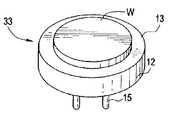
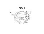
- FIG. 1is perspective view of a wafer carrier according to one of the present embodiments.
- FIGS. 2A and 2Bare cross-sectional views of a wafer carrier with an electrically insulating base substrate body.
- FIGS. 3A and 3Bare cross-sectional views of a wafer carrier with an electrically conducting base substrate body.
- FIG. 4is a cross-sectional view of a wafer carrier according to another embodiment.
- FIG. 5is a cross-sectional view of a wafer carrier according to still another embodiment.
- FIG. 6is a cross-section of one embodiment of an overcoat of the present invention having different layers of different resistivities.
- FIG. 7is a graph showing the volume resistivities for various materials along a temperature spectrum.
- FIG. 8is a micro-graph showing a cross section of an AlN overcoat consisting of 3 layers of two types of AlN with differing volume resistivity.
- the term “adjacent”includes both direct contact and lying near, as where an intervening layer exists between two layers or objects, or along side of another layer or object.
- the term “wafer carrier”may be used to denote a heater, an electrostatic chuck, or a combined heater/electrostatic chuck.
- circuitmay be used interchangeably with “electrode,” and the term “heating element” may be used interchangeably with “heating electrode,” “electrode,” “resistor,” “heating resistor,” or “heater.”
- the term “circuit”may be used in either the single or plural form, denoting that at least one unit is present.
- circuitmay be used interchangeably with “electrode,” and the term “electrode” may be used to denote either the single or plural form, denoting that at least one unit is present.
- heating elementmay be used interchangeably with “heating electrode,” “resistor,” “heating resistor,” or “heater.”
- the present embodimentsconcern a coated article for supporting a wafer in a process chamber.
- the coated articlemay be a heater, electrostatic chuck, wafer carrier, or similar article.
- the articlehas a body containing a base substrate and an electrode element deposited thereon, and also has an adjacent outer coating of dielectric material, such as aluminum nitride, which may be provided by chemical vapor deposition or other means (such as reactive physical vapor deposition, plasma spray, plasma-enhanced cvd, metal-organic cvd, photo-enhanced cvd).
- the outer coatinghas a plurality of zones or regions of differing electrical resistivity. The thicknesses or relative size of the different regions determines the overall bulk electrical resistivity of the coating.
- FIG. 1illustrates a wafer carrier 33 comprising a disk-shaped metallic, graphite or ceramic body 12 having an electrode disposed therein or thereon (not shown), and whose top surface 13 serves as a supporting surface for a substrate, e.g., a wafer W having a typical diameter of, e.g., 300 mm.
- the top surface 13is made of a high degree of flatness (within 0.05 mm surface variation) to further enhance the temperature control of the wafer W.
- Electric terminals 15 for supplying electricity to the wafer carriercan be attached at the center of the bottom surface of the body 12 , or in one embodiment, at the sides of the body 12 .
- one or more electrodescan be employed. Depending on the application, these electrodes may each function as a resistive heating element, an electromagnetic shielding electrode, a plasma-generating electrode, an electrostatic chuck electrode, or an electron-beam electrode. In one embodiment, two different electrodes are present, one acting as a heating element and the second as an electrostatic chuck electrode.
- the electrode(s)may be located within or on the base substrate of the wafer carrier toward the top (near the wafer substrate) or the bottom (away from the wafer substrate). A bottom location for the heating electrode may help diffuse localized heat generated by a pattern of the electrode and assist in the heat distribution to the wafer substrate.
- the electrodeis in the form of a film electrode and formed by processes known in the art including screen-printing, spin coating, plasma spray, thermal spray, spray pyrolysis, reactive spray deposition, sol-gel deposition, combustion torch, electric arc deposition, ion plating, physical vapor deposition, sputtering deposition, laser ablation, thermal evaporation, electroplating, and laser surface alloying.
- the film electrodecomprises a metal having a high melting point, e.g., iron, nickel, tungsten, tantalum, molybdenum, rhenium, and platinum or alloys thereof.
- the film electrodecomprises at least one of carbides or oxides of hafnium, zirconium, cerium, and mixtures thereof.
- an electrodeis in the form an elongated continuous strip of pyrolytic graphite.
- Pyrolytic graphite (“PG”)is first deposited onto the base substrate of the wafer carrier, via processes known in the art such as chemical vapor deposition. The PG is then is machined into a pre-determined pattern, e.g., a spiral, a serpentine, etc.
- the forming of the electrical pattern of the heating zones, i.e., an electrically isolated, resistive heater pathmay be done by techniques known in the art, including but not limited to micro machining, micro-brading, laser cutting, chemical etching, or e-beam etching.
- the base substrate of the bodycan be constructed of a bulk insulating material, such as ceramic.
- the base substratecan be made from a electrically conducting material that is then coated with an insulating layer.
- the base substrate 11 of the bodymay comprise an electrically insulating material (e.g., a sintered substrate) that may be selected from the group including oxides, nitrides, carbides, carbonitrides, and oxynitrides of elements selected from a group consisting of B, Al, Hf, Si, Ga, Y. refractory hard metals, transition metals; and combinations thereof.
- the base substrate 11may be characterized as having high wear resistance and high heat resistance properties.
- the base substratecomprises AlN of >99% purity and up to 5% of a sintering agent selected from Y 2 O 3 , Er 2 O 3 , and combinations thereof.
- the base substratecomprises pyrolytic boron nitride (pBN).
- a pBN base substratecan be substituted by (1) a pBN-coated graphite plate (the graphite plate being about 0.10-0.75 inches thick, optionally 0.12-0.50 inches thick, the pBN coating being about 0.005-0.035 inches, more preferably about 0.015-0.020 inches thick), (2) a hot-pressed boron nitride (BN) plate about 0.10-0.75 inches, more preferably about 0.25-0.50 inches thick, or (3) a pBN-coated hot-pressed BN plate (the hot-pressed BN plate being about 0.10-0.75 inches, more preferably about 0.25-0.50 inches thick, the PBN coating being about 0.005-0.035 inches, more preferably about 0.01-0.02 inches thick).
- a pBN-coated graphite platethe graphite plate being about 0.10-0.75 inches thick, optionally 0.12-0.50 inches thick, the pBN coating being about 0.005-0.035 inches, more preferably about 0.015-0.020 inches thick
- a heating electrode 14 having an optimized circuit designis formed on or embedded within the ceramic base substrate 11 .
- the electrode 14may comprise a material selected from the group of iron, nickel, tungsten, tantalum, molybdenum, rhenium and platinum or alloys thereof; carbides and nitrides of metals belonging to Groups IVa, Va and VIa of the Periodic Table; carbides or oxides of hafnium, zirconium, and cerium, and combinations thereof.
- the electrode 14may comprise a pyrolytic graphite (PG) or thermal pyrolytic graphite (TPG).
- the electrode 14comprises a material having a coefficient of thermal expansion (CTE) that closely matches the CTE of the base substrate 11 .
- CTEcoefficient of thermal expansion
- CTEsBy closely matching CTEs, it means one material having a CTE ranging from 0.75 to 1.25 the CTE of the base substrate. By closely matching the CTEs of the electrode and base substrate, this allows uniform repeated heating and cooling of the device without cracking or compromising the integrity of the device.
- the wafer carriercan also function as an electrostatic chuck.
- a chuck electrode 16e.g., a conductive layer such as formed from the materials above, a metallized film or a TPG electrode, is formed on the base substrate 11 using fabrication methods known in the art.
- an electrostatic chucksee U.S. Pat. Nos. 5,591,269; 5,566,043; 5,663,865; 5,606,484; 5,155,652; 5,665, 260; 5,909,355; and 5,693,581, the entire contents of which are incorporated herein by reference.
- the base substrate 11 and electrode(s)are coated with an overcoat 20 comprising AlN that is electrically insulating and comprising a plurality of zones or regions of differing electrical resistivities.
- an optional tie-layer(not shown) to help enhance the adhesion between the overcoat layer 20 and the base substrate 11 .
- the heater electrode 14is disposed on a bottom surface of the base substrate (away from the wafer substrate) to more easily spatially distribute and regulate heat in the wafer carrier.
- both the heater electrode 14 and the chucking electrode 16are disposed on the top of the base substrate.
- a separate insulating layer 20can be coated onto the base substrate and heater electrode prior to placement of the chucking electrode. This insulating layer can be formed of the same material as the base substrate, the overcoat, or a different material.
- FIGS. 3A-3BReferences are made to FIGS. 3A-3B for an embodiment of a wafer carrier having an electrically conductive base substrate 111 such as one with a graphite base substrate.
- graphiteis denoted as comprising the base substrate, depending on the application, other electrically conductive materials may be used, including but not limited to graphite; refractory metals such as W and Mo, transition metals, rare earth metals and alloys; oxides and carbides of hafnium, zirconium, and cerium, and mixtures thereof.
- the base substrate 111is coated with an insulating layer 130 that is electrically insulating, and optionally a tie-layer (not shown) to help enhance the adhesion between the insulating layer 130 and the base substrate 111 .
- the layermay comprise at least one of an oxide, nitride, carbide, carbonitride or oxynitride of elements selected from a group consisting of Hf, B, Al, Si, Ga, Y, refractory hard metals, transition metals; oxide, oxynitride of aluminum; and combinations thereof.
- An exampleis pyrolytic boron nitride (pBN).
- the layermay comprise at least one of: a nitride, carbide, carbonitride, boride, oxide, oxynitride of elements selected from Al, Si, refractory metals including Ta, W, Mo, transition metals including titanium, chromium, iron; and mixtures thereof.
- refractory metalsincluding Ta, W, Mo
- transition metalsincluding titanium, chromium, iron
- examplesinclude TiC, TaC, SiC, MoC, and mixtures thereof.
- Electrodes 134 , 136Deposited on the insulating layer 130 are one or more electrodes 134 , 136 . These electrodes may be similar in construction and function as heating 134 and chuck 136 electrodes, as in the embodiments described above. In one embodiment, as shown in FIG. 3A , the two electrodes 134 , 136 are on opposite sides of the base substrate. In another, they are on the same side, with an insulating layer 120 disposed between.
- either or both of the electrodescomprise a film electrode having a thickness ranging from 5-1000 ⁇ m, which is formed on an electrically insulating layer (either 130 or 120 depending on the embodiment) by processes known in the art.
- the film electrodecomprises a metal having a high melting point, e.g., iron, nickel, tantalum, tungsten, molybdenum, rhenium and platinum or alloys thereof.
- the film electrodecomprises at least one of carbides or oxides of hafnium, zirconium, cerium, and mixtures thereof.
- an electrolytic copper foil having a film thickness of 18 ⁇ mis used as electrode
- the base substrate and heaterare then further coated with an etch resistant overcoat 118 , that encases the base substrate and heater and forms a barrier between these elements and an operating atmosphere.
- the layermay comprise at least one of: a nitride, carbide, carbonitride, boride, oxide, oxynitride of elements selected from Al, Si, refractory metals including Ta, W, Mo, transition metals including titanium, chromium, iron; and mixtures thereof.
- refractory metalsincluding Ta, W, Mo
- transition metalsincluding titanium, chromium, iron
- examplesinclude TiC, TaC, SiC, MoC, and mixtures thereof.
- the wafer carriercan also contain a thermistor or thermocouple 250 , as shown in FIG. 4 , and/or an electro-magnetic shield 252 , as shown in FIG. 5 .
- the electromagnetic shieldcan function to eliminate the electrical interference between the chucking electrode 236 and the heating elements 234 , or between the heating elements and the wafer.
- the overcoatcomprises one or more regions or layers having different volume resistivities.
- the overcoatcomprises at least two different materials selected from the group including: an oxide, nitride, carbide, carbonitride or oxynitride of elements selected from a group consisting of Hf, B, Al, Si, Ga, Y, refractory hard metals, transition metals; oxide, oxynitride of aluminum; and combinations thereof; a high thermal stability zirconium phosphate having an NZP structure of NaZr 2 (PO 4 ) 3 ; a glass-ceramic composition containing at least one element selected from the group consisting of elements of the group 2 a , group 3 a and group 4 a ; a BaO—Al 2 O 3 —B 2 O 3 —SiO 2 glass; and a mixture of SiO 2 and a plasma-resistant material comprising an oxide of Y, Sc, La, Ce, Gd,
- the two or more regions having different volume resistivitiescomprise layers 80 , 82 , 84 , each of the layers being made from a material having different resistivity values, R 1 , R 2 , and R 3 , wherein R 1 , R 2 , and R 3 are simply the specific resistance (resistivity) of the material in the layer times the layer thickness, L.
- layer 80is considered to be the layer adjacent the wafer carrier body or electrodes while layer 84 is considered to be the outer layer in contact with the wafer processing chamber environment.
- layer 84is considered to be the outer layer in contact with the wafer processing chamber environment.
- the embodiment shown in FIG. 6has three different layers, the number of layers in the invention is not so limited and can be any number greater than or equal to two. However, it should be recognized that production cost and complexity generally increases as the number of layers increases.
- the various layerscan have relatively fine, distinct dividing lines between them, or they can be diffuse or graded, with significant interpenetration of each layer into the other and no apparent demarcation line between them.
- the layerscan each comprise AlN, or other materials having similar CTE's. However, it is preferred for the outermost layer 84 to comprise AlN, due to its excellent resistance to corrosion in wafer processing environments.
- each of the layerscomprise a material that includes AlN, wherein the volume resistivity of the AlN in each of the layers is different.
- the resistivity of AlNcan be changed. This include without limitation 1) changing the density of AlN by the inclusion of various defects or pores in the bulk material, or through other methods, 2) changing the stoichiometry of the material by changing the Al to N ratio in the material, 3) introducing impurities or dopants such as oxygen or carbon into the AlN material, 4) changing or altering the AlN crystal orientation, crystal structure or crystal size, and 5) changing the number of pores, pore size, pore shape, or pore location in the AlN layer. Methods 4) and 5) above can be considered as changing the microstructure of the AlN.
- Methods of modifying the density, crystal structure, stoichiometry, impurity composition, and defectsinclude varying the conditions under which the AlN is deposited, such as varying temperatures, pressures, precursor concentrations, gas flow rates, plasma energy densities, and substrate surface conditions, and other variations to process conditions.
- the overcoatingcomprises three layers, wherein the top and bottom layer comprise AlN having a volume resistivity of about 10 5 ohm-cm at 600° C.
- the middle layercomprises a blend of AlN and Al 2 O 3 having a lower volume resistivity, e.g. about 10 10 ohm-cm at 600° C.
- the entire thickness of the coatingmay be from about 5 um-1000 um.
- the thicknesses of the individual layersmay be from 1 um-999 um.
- the preferred entire thicknessis from about 25 um-500 um, and the preferred thickness of individual layers is from about 5 um-495 um.
- the coatingmay include 1) regions wherein the region adjacent the electrode is aluminum nitride and at least one region not in contact with the electrode comprises aluminum oxynitride, 2) a region adjacent the electrode has at least 25% lower electrical resistivity as compared to the bulk coating and at least one region not adjacent with the electrode has at least 25% higher electrical resistivity as compared to the bulk resisitivity of the coating, 3) a region adjacent the electrode comprising aluminum nitride comprising less than 0.6 wt % oxygen and at least one zone not adjacent the electrode is aluminum nitride comprising greater than 0.6 wt % oxygen, 4) a region adjacent the electrode comprising aluminum nitride having a 25° C. electrical resistivity between 10 ⁇ 3 and 10 14 ohm-cm and at least one zone not adjacent the electrode having a 25° C. electrical resistivity greater than the first region and between 10 9 and 10 15 ohm-cm.
- a wafer carrier according to the inventionis used in the processing of silicon wafers. Part of this processing involves layering of materials on the wafer by chemical vapor deposition, the wafer carrier is also subject to being coated with the materials during the processing. It becomes periodically necessary to clean the wafer carrier. The process of layering materials on the wafer is generally not damaging to the wafer carrier. However, harsh cleaning compositions such as NF 3 plasma are often used to clean the surface of these articles. This cleaning is typically undertaken after 30 to 40 process hours, or hours spent processing wafers. The wafer carrier is then typically subjected to plasma cleaning for 1-2 cleaning hours or less. A wafer carrier coated only with PBN is typically damaged sufficiently to require replacement after exposure to NF 3 plasma for 50 to 100 cleaning hours.
- CVD-AlN coatingis considerably more resistant to attack by NF 3 plasma than a PBN coating, and in testing has shown no detectable damage after 12-24 cleaning hours.
- a wafer carrier according to the inventionpreferably has sufficient CVD-AlN coating to effectively survive, that is, to maintain the article in a protected condition such that the coated article does not need to be replaced, for at least 10, 25, 50, 100, 200, 300, 400, 500, 600, 700, 800, 900, 1000, 1500, 2000, 3000, or 4000 cleaning hours, that is, hours of NF 3 plasma attack during cleaning of the article.
- outer coating 18 , 118preferably comprises CVD-AlN and is about 5-1000 microns, more preferably about 25-500 microns.
- the process of applying a CVD-AlN coatingis known; see, for example, U.S. Pat. Nos. 4,950,558; 5,672,420; 4,239,819; 5,178,911; 4,172,754; and 5,356,608, the contents of which are incorporated by reference.
- the vapor deposition processis performed in a reactor having a chlorination chamber in communication with a deposition chamber.
- the deposition chamberis contained within a vacuum chamber, which is connected to one or more vacuum pumps.
- the coating substrateis placed in the deposition chamber and the chlorination chamber is loaded with a bed of aluminum particles.
- the vacuum chamber and deposition chamberare then evacuated.
- the chlorination chamberis heated to a temperature between 200 and 400° C. by resistive heating elements. Chlorine (Cl 2 ) and nitrogen (N 2 ) gas are introduced into the chlorination chamber. At this temperature the aluminum and chlorine form aluminum chloride gas.
- the aluminum chloridethen passes into deposition chamber, which had previously been evacuated to a low pressure of about 1 to 10 torr, preferably about 2 torr.
- Ammonia (NH 3 ) and hydrogen (H 2 )are also introduced into the deposition chamber.
- the temperatureis maintained at 600 to 1100° C., by heaters.
- the wafer carrier substrateis then coated with AlN as the aluminum chloride and ammonia react to form AlN.
- the AlN coatingbuilds up on the wafer carrier substrate at a rate ranging from about 10 to 20 micrometers per hour.
- the aluminum nitride coating resulting from chemical vapor depositionis superior to that resulting from sintering or hot-pressing, as it is very dense and highly pure, and has an essentially uniform thickness.
- Other CVD-AlN coating processesare known in the art using other techniques and materials, all of which art is incorporated herein by reference.
- FIG. 7shows that the resistivity of CVD deposited Aluminum Nitride coatings are in the Johnson-Rahbeck regime and comparable to resistivity of carbon-doped pyrolitic boron nitride materials (CPBN).
- the region designated Ais the Johnson-Rahbeck regime according to Tamagawa, J Vac. Sci. Japan 45 (2002).
- the region designated Bis the Johnson-Rahbeck regime according to Kahno et al., JVSTB 21, pp 2371 (2003).
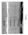
- Examples of the layered AlNare shown in Table 1 and in FIG. 8 .
- the examplesutilize 3 types of AlN film with varying resistivity.
- Type-A AlNis a low-density, low resistivity film
- Type-B AlNis a high density, mid-range resistivity film
- Type-C AlNis an ultra-high resistivity AlN film.
- the resistivity measured at 600 C. for each AlN typeis shown in Table 1.
- Sample 70858consists of 3 layers of AlN, in which layers 1 and 3 are Type-A AlN and layer 2 is Type-B AlN.
- the composite resistivity of the tri-layer coatingfalls between the resistivity of the individual layers, and is tuned to 1.5 ⁇ 10 7 ohm-cm by controlling the thickness of the individual layers.
- Sample 80153is a bi-layer structure, in which the resistivity was tuned from 1.3 ⁇ 10 10 ohm-cm, if only Type-C AlN was used, to 4.1 ⁇ 10 9 ohm-cm.
- a third exampleis provided showing the a tri-layer structure utilizing Type-B and Type-C AlN, in which the composite resistivity of the tri-layer structure is tuned to 6.9 ⁇ 10 8 ohm-cm.
- FIG. 8is an SEM micro-graph showing the cross section of an AlN overcoating consisting of 3 layers of two types of AlN with differing volume resistivity.
Landscapes
- Engineering & Computer Science (AREA)
- Physics & Mathematics (AREA)
- Condensed Matter Physics & Semiconductors (AREA)
- General Physics & Mathematics (AREA)
- Manufacturing & Machinery (AREA)
- Computer Hardware Design (AREA)
- Microelectronics & Electronic Packaging (AREA)
- Power Engineering (AREA)
- Container, Conveyance, Adherence, Positioning, Of Wafer (AREA)
Abstract
Description
ρ=resistivity=(R×A)/L
(ρ×L)/A=R, and
RT=(ρT×LT)/A=(ρ×L1)/A+(ρ2×L2)/A+ . . . (ρn×Ln)/A
RT=(ρT×LT)=(ρ1×L1)+(ρ2×L2)+ . . . (ρn×Ln)
| TABLE 1 | |||||||
| thk | 600 C. resistivity | ||||||
| Sample | Structure | AIN Type | (cm2) | (um) | R (ohm) | (ohm-cm) | |
| 70858 | Type-A | 9 | 75 | 3.67E+01 | 4.4E+04 | ||
| layer 2 | Type-B | 9 | 80 | 3.91E+04 | 4.4E+07 | ||
| layer 3 | Type-A | 9 | 75 | 3.67E+01 | 4.4E+04 | ||
| Composite | Type-A/Type-B/Type-A | 9 | 230 | 3.92E+04 | 1.5E+07 | ||
| 80153 | Type-C | 9 | 42 | 6.07E+06 | 1.3E+10 | ||
| layer 2 | Type-A | 9 | 90 | 4.40E+01 | 4.4E+04 | ||
| Composite | Type-A/Type-C | 9 | 132 | 6.07E+06 | 4.1E+09 | ||
| layer | 1 | Type-B | 9 | 95 | 4.64E+04 | 4.4E+07 | |
| layer 2 | Type-C | 9 | 10 | 1.44E+06 | 1.3E+10 | ||
| layer 3 | Type-B | 9 | 95 | 4.64E+04 | 4.4E+07 | ||
| Composite | Type-B/Type-C/Type-B | 9 | 200 | 1.54E+06 | 6.9E+08 | ||
Claims (22)
Priority Applications (5)
| Application Number | Priority Date | Filing Date | Title |
|---|---|---|---|
| US12/204,079US7929269B2 (en) | 2008-09-04 | 2008-09-04 | Wafer processing apparatus having a tunable electrical resistivity |
| CN200980143906.6ACN102203931B (en) | 2008-09-04 | 2009-09-02 | Wafer processing apparatus having a tunable electrical resistivity |
| JP2011526145AJP5524213B2 (en) | 2008-09-04 | 2009-09-02 | Wafer processing apparatus with adjustable electrical resistivity |
| PCT/US2009/055702WO2010028023A1 (en) | 2008-09-04 | 2009-09-02 | Wafer processing apparatus having a tunable electrical resistivity |
| EP09792160AEP2335279A1 (en) | 2008-09-04 | 2009-09-02 | Wafer processing apparatus having a tunable electrical resistivity |
Applications Claiming Priority (1)
| Application Number | Priority Date | Filing Date | Title |
|---|---|---|---|
| US12/204,079US7929269B2 (en) | 2008-09-04 | 2008-09-04 | Wafer processing apparatus having a tunable electrical resistivity |
Publications (2)
| Publication Number | Publication Date |
|---|---|
| US20100053841A1 US20100053841A1 (en) | 2010-03-04 |
| US7929269B2true US7929269B2 (en) | 2011-04-19 |
Family
ID=41562602
Family Applications (1)
| Application Number | Title | Priority Date | Filing Date |
|---|---|---|---|
| US12/204,079Expired - Fee RelatedUS7929269B2 (en) | 2008-09-04 | 2008-09-04 | Wafer processing apparatus having a tunable electrical resistivity |
Country Status (5)
| Country | Link |
|---|---|
| US (1) | US7929269B2 (en) |
| EP (1) | EP2335279A1 (en) |
| JP (1) | JP5524213B2 (en) |
| CN (1) | CN102203931B (en) |
| WO (1) | WO2010028023A1 (en) |
Cited By (3)
| Publication number | Priority date | Publication date | Assignee | Title |
|---|---|---|---|---|
| US9887121B2 (en)* | 2013-04-26 | 2018-02-06 | Applied Materials, Inc. | Protective cover for electrostatic chuck |
| US20210384014A1 (en)* | 2019-03-18 | 2021-12-09 | Ngk Insulators, Ltd. | Ceramic heater |
| US20220181126A1 (en)* | 2019-03-14 | 2022-06-09 | Lam Research Corporation | Lamellar ceramic structure |
Families Citing this family (34)
| Publication number | Priority date | Publication date | Assignee | Title |
|---|---|---|---|---|
| WO2012019017A2 (en)* | 2010-08-06 | 2012-02-09 | Applied Materials, Inc. | Electrostatic chuck and methods of use thereof |
| EP2742525A4 (en)* | 2011-08-10 | 2015-04-01 | Entegris Inc | Aion coated substrate with optional yttria overlayer |
| KR101372333B1 (en)* | 2012-02-16 | 2014-03-14 | 주식회사 유진테크 | Substrate processing module and substrate processing apparatus including the same |
| US9034199B2 (en) | 2012-02-21 | 2015-05-19 | Applied Materials, Inc. | Ceramic article with reduced surface defect density and process for producing a ceramic article |
| US9212099B2 (en) | 2012-02-22 | 2015-12-15 | Applied Materials, Inc. | Heat treated ceramic substrate having ceramic coating and heat treatment for coated ceramics |
| CN103302431B (en)* | 2012-03-09 | 2016-03-02 | 鸿富锦精密工业(深圳)有限公司 | Chip welding device |
| US9090046B2 (en) | 2012-04-16 | 2015-07-28 | Applied Materials, Inc. | Ceramic coated article and process for applying ceramic coating |
| US9394615B2 (en) | 2012-04-27 | 2016-07-19 | Applied Materials, Inc. | Plasma resistant ceramic coated conductive article |
| US9604249B2 (en) | 2012-07-26 | 2017-03-28 | Applied Materials, Inc. | Innovative top-coat approach for advanced device on-wafer particle performance |
| US9343289B2 (en) | 2012-07-27 | 2016-05-17 | Applied Materials, Inc. | Chemistry compatible coating material for advanced device on-wafer particle performance |
| CN104704608B (en)* | 2012-09-13 | 2017-03-22 | 松下知识产权经营株式会社 | Nitride semiconductor structure |
| JP2014093420A (en)* | 2012-11-02 | 2014-05-19 | Toyota Motor Corp | Jig for bonding wafer to support disk and semiconductor device manufacturing method using the same |
| US9916998B2 (en) | 2012-12-04 | 2018-03-13 | Applied Materials, Inc. | Substrate support assembly having a plasma resistant protective layer |
| US9685356B2 (en) | 2012-12-11 | 2017-06-20 | Applied Materials, Inc. | Substrate support assembly having metal bonded protective layer |
| US8941969B2 (en)* | 2012-12-21 | 2015-01-27 | Applied Materials, Inc. | Single-body electrostatic chuck |
| US9358702B2 (en) | 2013-01-18 | 2016-06-07 | Applied Materials, Inc. | Temperature management of aluminium nitride electrostatic chuck |
| US9669653B2 (en) | 2013-03-14 | 2017-06-06 | Applied Materials, Inc. | Electrostatic chuck refurbishment |
| US9543183B2 (en)* | 2013-04-01 | 2017-01-10 | Fm Industries, Inc. | Heated electrostatic chuck and semiconductor wafer heater and methods for manufacturing same |
| US9666466B2 (en) | 2013-05-07 | 2017-05-30 | Applied Materials, Inc. | Electrostatic chuck having thermally isolated zones with minimal crosstalk |
| US9865434B2 (en) | 2013-06-05 | 2018-01-09 | Applied Materials, Inc. | Rare-earth oxide based erosion resistant coatings for semiconductor application |
| CN104241182B (en)* | 2013-06-08 | 2017-07-25 | 中微半导体设备(上海)有限公司 | The manufacture method of electrostatic chuck, electrostatic chuck and plasma processing apparatus |
| US9850568B2 (en) | 2013-06-20 | 2017-12-26 | Applied Materials, Inc. | Plasma erosion resistant rare-earth oxide based thin film coatings |
| KR102119867B1 (en)* | 2013-10-21 | 2020-06-09 | 주식회사 미코세라믹스 | Electrostatic chuck |
| JP6277015B2 (en)* | 2014-02-28 | 2018-02-07 | 株式会社日立ハイテクノロジーズ | Plasma processing equipment |
| US9740111B2 (en)* | 2014-05-16 | 2017-08-22 | Applied Materials, Inc. | Electrostatic carrier for handling substrates for processing |
| US10020218B2 (en) | 2015-11-17 | 2018-07-10 | Applied Materials, Inc. | Substrate support assembly with deposited surface features |
| JP2018060905A (en)* | 2016-10-05 | 2018-04-12 | 株式会社ディスコ | Electrostatic chuck plate and method of manufacturing electrostatic chuck plate |
| US20180374736A1 (en)* | 2017-06-22 | 2018-12-27 | Applied Materials, Inc. | Electrostatic carrier for die bonding applications |
| JP6935132B2 (en)* | 2017-07-21 | 2021-09-15 | 株式会社ディスコ | Manufacturing method of electrostatic chuck plate |
| US11047035B2 (en) | 2018-02-23 | 2021-06-29 | Applied Materials, Inc. | Protective yttria coating for semiconductor equipment parts |
| US12381110B2 (en)* | 2020-02-13 | 2025-08-05 | Jabil Inc. | Apparatus, system and method for providing a substrate chuck |
| WO2022046830A1 (en)* | 2020-08-25 | 2022-03-03 | Momentive Performance Materials Quartz, Inc. | Graphite based thermal leveler with high thermal conductivity material encapsulated therein |
| JP7465771B2 (en)* | 2020-09-15 | 2024-04-11 | 日本碍子株式会社 | Compound sintered body, semiconductor manufacturing equipment member, and method for manufacturing compound sintered body |
| JP7718902B2 (en)* | 2021-08-06 | 2025-08-05 | 株式会社フェローテックマテリアルテクノロジーズ | Wafer Support |
Citations (26)
| Publication number | Priority date | Publication date | Assignee | Title |
|---|---|---|---|---|
| US4384918A (en) | 1980-09-30 | 1983-05-24 | Fujitsu Limited | Method and apparatus for dry etching and electrostatic chucking device used therein |
| JPH07226431A (en) | 1994-02-09 | 1995-08-22 | Kyocera Corp | Electrostatic chuck |
| JPH0851001A (en) | 1994-08-09 | 1996-02-20 | Kyocera Corp | Ceramic resistor |
| JPH0878202A (en) | 1994-09-01 | 1996-03-22 | Kyocera Corp | Ceramic resistor |
| JPH08102485A (en) | 1994-09-30 | 1996-04-16 | Kyocera Corp | Electrostatic chuck |
| JPH08153603A (en) | 1994-11-29 | 1996-06-11 | Kyocera Corp | Ceramic resistor |
| JPH08157263A (en) | 1994-11-30 | 1996-06-18 | Kyocera Corp | Ceramic resistor |
| US5663865A (en) | 1995-02-20 | 1997-09-02 | Shin-Etsu Chemical Co., Ltd. | Ceramic electrostatic chuck with built-in heater |
| US5668524A (en) | 1994-02-09 | 1997-09-16 | Kyocera Corporation | Ceramic resistor and electrostatic chuck having an aluminum nitride crystal phase |
| US5702764A (en) | 1993-12-22 | 1997-12-30 | Shin-Etsu Chemical Co., Ltd. | Method for the preparation of pyrolytic boron nitride-clad double-coated article |
| US5748436A (en) | 1996-10-02 | 1998-05-05 | Advanced Ceramics Corporation | Ceramic electrostatic chuck and method |
| WO1999029030A1 (en) | 1997-12-02 | 1999-06-10 | Applied Materials, Inc. | Improved ceramic electrostatic chuck and method of fabricating same |
| US5928960A (en) | 1996-10-24 | 1999-07-27 | International Business Machines Corporation | Process for reducing pattern factor effects in CMP planarization |
| EP0768389B1 (en) | 1995-10-03 | 2000-08-16 | Advanced Ceramics Corporation | Pyrolytic boron nitride compact and method of manufacture |
| US6122159A (en) | 1997-12-12 | 2000-09-19 | Shin Etsu-Chemical Co., Ltd. | Electrostatic holding apparatus |
| US6351367B1 (en) | 1997-09-30 | 2002-02-26 | Shin-Etsu Chemical Co., Ltd. | Electrostatic holding apparatus having insulating layer with enables easy attachment and detachment of semiconductor object |
| US6410172B1 (en) | 1999-11-23 | 2002-06-25 | Advanced Ceramics Corporation | Articles coated with aluminum nitride by chemical vapor deposition |
| US6535372B2 (en) | 2001-06-20 | 2003-03-18 | Applied Materials, Inc. | Controlled resistivity boron nitride electrostatic chuck apparatus for retaining a semiconductor wafer and method of fabricating the same |
| US20040011770A1 (en) | 2000-10-25 | 2004-01-22 | Strang Eric J. | Method of and structure for controlling electrode temperature |
| US6953918B2 (en) | 2002-11-01 | 2005-10-11 | Shin-Etsu Chemical Co., Ltd. | Heating apparatus which has electrostatic adsorption function, and method for producing it |
| EP1220311B1 (en) | 2000-12-11 | 2007-02-14 | GE Specialty Materials Japan Co., Ltd. | Electrostatic chuck and method of manufacturing the same |
| JP2007109827A (en) | 2005-10-12 | 2007-04-26 | Toto Ltd | Electrostatic chuck |
| WO2007058605A1 (en) | 2005-11-18 | 2007-05-24 | Replisaurus Technologies Ab | Master electrode and method of forming it |
| US20080016684A1 (en)* | 2006-07-06 | 2008-01-24 | General Electric Company | Corrosion resistant wafer processing apparatus and method for making thereof |
| US20080186647A1 (en) | 2007-02-07 | 2008-08-07 | Ngk Insulators, Ltd. | Electrostatic chuck and method of manufacturing the same |
| US20090242544A1 (en)* | 2005-10-12 | 2009-10-01 | Shin-Etsu Chemical Co., Ltd. | Wafer heating apparatus having electrostatic attraction function |
Family Cites Families (8)
| Publication number | Priority date | Publication date | Assignee | Title |
|---|---|---|---|---|
| JPH10154745A (en)* | 1996-11-26 | 1998-06-09 | Hitachi Ltd | Electrostatic suction device |
| JP4499431B2 (en)* | 2003-07-07 | 2010-07-07 | 日本碍子株式会社 | Aluminum nitride sintered body, electrostatic chuck, conductive member, member for semiconductor manufacturing apparatus, and method for manufacturing aluminum nitride sintered body |
| JP4744855B2 (en)* | 2003-12-26 | 2011-08-10 | 日本碍子株式会社 | Electrostatic chuck |
| JP2005317749A (en)* | 2004-04-28 | 2005-11-10 | Sumitomo Electric Ind Ltd | Semiconductor manufacturing apparatus holder and semiconductor manufacturing apparatus equipped with the same |
| JP2006060040A (en)* | 2004-08-20 | 2006-03-02 | Rasa Ind Ltd | Electrostatically chucking plate, and manufacturing method thereof |
| JP2006089345A (en)* | 2004-09-27 | 2006-04-06 | Kyocera Corp | Conductive porous ceramic sintered body and method for producing the same |
| US7446284B2 (en)* | 2005-12-21 | 2008-11-04 | Momentive Performance Materials Inc. | Etch resistant wafer processing apparatus and method for producing the same |
| CN101101887A (en)* | 2006-07-06 | 2008-01-09 | 通用电气公司 | Corrosion resistant wafer processing apparatus and method for making thereof |
- 2008
- 2008-09-04USUS12/204,079patent/US7929269B2/ennot_activeExpired - Fee Related
- 2009
- 2009-09-02WOPCT/US2009/055702patent/WO2010028023A1/enactiveApplication Filing
- 2009-09-02JPJP2011526145Apatent/JP5524213B2/ennot_activeExpired - Fee Related
- 2009-09-02CNCN200980143906.6Apatent/CN102203931B/ennot_activeExpired - Fee Related
- 2009-09-02EPEP09792160Apatent/EP2335279A1/ennot_activeWithdrawn
Patent Citations (27)
| Publication number | Priority date | Publication date | Assignee | Title |
|---|---|---|---|---|
| US4384918A (en) | 1980-09-30 | 1983-05-24 | Fujitsu Limited | Method and apparatus for dry etching and electrostatic chucking device used therein |
| US5702764A (en) | 1993-12-22 | 1997-12-30 | Shin-Etsu Chemical Co., Ltd. | Method for the preparation of pyrolytic boron nitride-clad double-coated article |
| US5777543A (en) | 1994-01-09 | 1998-07-07 | Kyocera Corporation | Ceramic resistor and electrostatic chuck having an aluminum nitride crystal phase |
| US5668524A (en) | 1994-02-09 | 1997-09-16 | Kyocera Corporation | Ceramic resistor and electrostatic chuck having an aluminum nitride crystal phase |
| JPH07226431A (en) | 1994-02-09 | 1995-08-22 | Kyocera Corp | Electrostatic chuck |
| JPH0851001A (en) | 1994-08-09 | 1996-02-20 | Kyocera Corp | Ceramic resistor |
| JPH0878202A (en) | 1994-09-01 | 1996-03-22 | Kyocera Corp | Ceramic resistor |
| JPH08102485A (en) | 1994-09-30 | 1996-04-16 | Kyocera Corp | Electrostatic chuck |
| JPH08153603A (en) | 1994-11-29 | 1996-06-11 | Kyocera Corp | Ceramic resistor |
| JPH08157263A (en) | 1994-11-30 | 1996-06-18 | Kyocera Corp | Ceramic resistor |
| US5663865A (en) | 1995-02-20 | 1997-09-02 | Shin-Etsu Chemical Co., Ltd. | Ceramic electrostatic chuck with built-in heater |
| EP0768389B1 (en) | 1995-10-03 | 2000-08-16 | Advanced Ceramics Corporation | Pyrolytic boron nitride compact and method of manufacture |
| US5748436A (en) | 1996-10-02 | 1998-05-05 | Advanced Ceramics Corporation | Ceramic electrostatic chuck and method |
| US5928960A (en) | 1996-10-24 | 1999-07-27 | International Business Machines Corporation | Process for reducing pattern factor effects in CMP planarization |
| US6351367B1 (en) | 1997-09-30 | 2002-02-26 | Shin-Etsu Chemical Co., Ltd. | Electrostatic holding apparatus having insulating layer with enables easy attachment and detachment of semiconductor object |
| WO1999029030A1 (en) | 1997-12-02 | 1999-06-10 | Applied Materials, Inc. | Improved ceramic electrostatic chuck and method of fabricating same |
| US6122159A (en) | 1997-12-12 | 2000-09-19 | Shin Etsu-Chemical Co., Ltd. | Electrostatic holding apparatus |
| US6410172B1 (en) | 1999-11-23 | 2002-06-25 | Advanced Ceramics Corporation | Articles coated with aluminum nitride by chemical vapor deposition |
| US20040011770A1 (en) | 2000-10-25 | 2004-01-22 | Strang Eric J. | Method of and structure for controlling electrode temperature |
| EP1220311B1 (en) | 2000-12-11 | 2007-02-14 | GE Specialty Materials Japan Co., Ltd. | Electrostatic chuck and method of manufacturing the same |
| US6535372B2 (en) | 2001-06-20 | 2003-03-18 | Applied Materials, Inc. | Controlled resistivity boron nitride electrostatic chuck apparatus for retaining a semiconductor wafer and method of fabricating the same |
| US6953918B2 (en) | 2002-11-01 | 2005-10-11 | Shin-Etsu Chemical Co., Ltd. | Heating apparatus which has electrostatic adsorption function, and method for producing it |
| JP2007109827A (en) | 2005-10-12 | 2007-04-26 | Toto Ltd | Electrostatic chuck |
| US20090242544A1 (en)* | 2005-10-12 | 2009-10-01 | Shin-Etsu Chemical Co., Ltd. | Wafer heating apparatus having electrostatic attraction function |
| WO2007058605A1 (en) | 2005-11-18 | 2007-05-24 | Replisaurus Technologies Ab | Master electrode and method of forming it |
| US20080016684A1 (en)* | 2006-07-06 | 2008-01-24 | General Electric Company | Corrosion resistant wafer processing apparatus and method for making thereof |
| US20080186647A1 (en) | 2007-02-07 | 2008-08-07 | Ngk Insulators, Ltd. | Electrostatic chuck and method of manufacturing the same |
Cited By (7)
| Publication number | Priority date | Publication date | Assignee | Title |
|---|---|---|---|---|
| US9887121B2 (en)* | 2013-04-26 | 2018-02-06 | Applied Materials, Inc. | Protective cover for electrostatic chuck |
| US10177023B2 (en) | 2013-04-26 | 2019-01-08 | Applied Materials, Inc. | Protective cover for electrostatic chuck |
| US10541171B2 (en) | 2013-04-26 | 2020-01-21 | Applied Materials, Inc. | Protective cover for electrostatic chuck |
| US20220181126A1 (en)* | 2019-03-14 | 2022-06-09 | Lam Research Corporation | Lamellar ceramic structure |
| US12368029B2 (en)* | 2019-03-14 | 2025-07-22 | Lam Research Corporation | Lamellar ceramic structure |
| US20210384014A1 (en)* | 2019-03-18 | 2021-12-09 | Ngk Insulators, Ltd. | Ceramic heater |
| US12165855B2 (en)* | 2019-03-18 | 2024-12-10 | Ngk Insulators, Ltd. | Ceramic heater |
Also Published As
| Publication number | Publication date |
|---|---|
| CN102203931A (en) | 2011-09-28 |
| US20100053841A1 (en) | 2010-03-04 |
| CN102203931B (en) | 2014-08-20 |
| WO2010028023A1 (en) | 2010-03-11 |
| JP2012502478A (en) | 2012-01-26 |
| JP5524213B2 (en) | 2014-06-18 |
| EP2335279A1 (en) | 2011-06-22 |
Similar Documents
| Publication | Publication Date | Title |
|---|---|---|
| US7929269B2 (en) | Wafer processing apparatus having a tunable electrical resistivity | |
| CN101026119B (en) | Etch resistant wafer processing apparatus and method for producing the same | |
| US7901509B2 (en) | Heating apparatus with enhanced thermal uniformity and method for making thereof | |
| US6410172B1 (en) | Articles coated with aluminum nitride by chemical vapor deposition | |
| CN101501834B (en) | Electrostatic chuck device | |
| KR101310521B1 (en) | Heating apparatus with enhanced thermal uniformity and method for making thereof | |
| KR101800337B1 (en) | Electrostatic chuck device | |
| CN101116170B (en) | Packaged chip processing device and manufacturing method thereof | |
| US20080141938A1 (en) | Processing apparatus, coated article and method | |
| US20030047283A1 (en) | Apparatus for supporting a substrate and method of fabricating same | |
| JP2008042140A (en) | Electrostatic chuck device | |
| EP1416520A1 (en) | Heating apparatus with electrostatic attraction function and method for producing it | |
| US8115141B2 (en) | Heating element | |
| CN110662314B (en) | Heater and preparation method thereof | |
| US20090308859A1 (en) | Ceramic heater and method of manufacturing the same | |
| WO2002001611A2 (en) | Electrostatic chuck and method of fabricating the same | |
| KR20000023534A (en) | Structural body and method of producing the same | |
| JP2004079734A (en) | Heating device | |
| KR20230096465A (en) | Method for Manufacturing Ceramic Susceptor | |
| JP4166383B2 (en) | Structure and manufacturing method thereof | |
| JP2001176646A (en) | Ceramic heater | |
| JP2001223066A (en) | Ceramic heater |
Legal Events
| Date | Code | Title | Description |
|---|---|---|---|
| AS | Assignment | Owner name:MOMENTIVE PERFORMANCE MATERIALS INC.,NEW YORK Free format text:ASSIGNMENT OF ASSIGNORS INTEREST;ASSIGNORS:RUSINKO, DAVID MICHAEL, JR.;SCHAEPKENS, MARC;ZENG, WANXUE;SIGNING DATES FROM 20080813 TO 20080829;REEL/FRAME:021481/0243 Owner name:MOMENTIVE PERFORMANCE MATERIALS INC., NEW YORK Free format text:ASSIGNMENT OF ASSIGNORS INTEREST;ASSIGNORS:RUSINKO, DAVID MICHAEL, JR.;SCHAEPKENS, MARC;ZENG, WANXUE;SIGNING DATES FROM 20080813 TO 20080829;REEL/FRAME:021481/0243 | |
| AS | Assignment | Owner name:THE BANK OF NEW YORK MELLON TRUST COMPANY, N.A., A Free format text:SECURITY AGREEMENT;ASSIGNORS:MOMENTIVE PERFORMANCE MATERIALS, INC.;JUNIPER BOND HOLDINGS I LLC;JUNIPER BOND HOLDINGS II LLC;AND OTHERS;REEL/FRAME:022902/0461 Effective date:20090615 | |
| FEPP | Fee payment procedure | Free format text:PAYER NUMBER DE-ASSIGNED (ORIGINAL EVENT CODE: RMPN); ENTITY STATUS OF PATENT OWNER: LARGE ENTITY Free format text:PAYOR NUMBER ASSIGNED (ORIGINAL EVENT CODE: ASPN); ENTITY STATUS OF PATENT OWNER: LARGE ENTITY | |
| STCF | Information on status: patent grant | Free format text:PATENTED CASE | |
| AS | Assignment | Owner name:BANK OF NEW YORK MELLON TRUST COMPANY, N.A., THE, PENNSYLVANIA Free format text:SECURITY AGREEMENT;ASSIGNOR:MOMENTIVE PERFORMANCE MATERIALS INC;REEL/FRAME:028344/0208 Effective date:20120525 Owner name:BANK OF NEW YORK MELLON TRUST COMPANY, N.A., THE, Free format text:SECURITY AGREEMENT;ASSIGNOR:MOMENTIVE PERFORMANCE MATERIALS INC;REEL/FRAME:028344/0208 Effective date:20120525 | |
| AS | Assignment | Owner name:BANK OF NEW YORK MELLON TRUST COMPANY, N.A., THE, PENNSYLVANIA Free format text:PATENT SECURITY AGREEMENT;ASSIGNOR:MOMENTIVE PERFORMANCE MATERIALS INC.;REEL/FRAME:030185/0001 Effective date:20121116 Owner name:BANK OF NEW YORK MELLON TRUST COMPANY, N.A., THE, Free format text:PATENT SECURITY AGREEMENT;ASSIGNOR:MOMENTIVE PERFORMANCE MATERIALS INC.;REEL/FRAME:030185/0001 Effective date:20121116 | |
| AS | Assignment | Owner name:JPMORGAN CHASE BANK, N.A., NEW YORK Free format text:SECURITY AGREEMENT;ASSIGNOR:MOMENTIVE PERFORMANCE MATERIALS INC.;REEL/FRAME:030311/0343 Effective date:20130424 | |
| FPAY | Fee payment | Year of fee payment:4 | |
| AS | Assignment | Owner name:THE BANK OF NEW YORK MELLON TRUST COMPANY, N.A., AS COLLATERAL AGENT, PENNSYLVANIA Free format text:SECURITY INTEREST;ASSIGNOR:MOMENTIVE PERFORMANCE MATERIALS INC.;REEL/FRAME:034066/0570 Effective date:20141024 Owner name:THE BANK OF NEW YORK MELLON TRUST COMPANY, N.A., AS COLLATERAL AGENT, PENNSYLVANIA Free format text:SECURITY INTEREST;ASSIGNOR:MOMENTIVE PERFORMANCE MATERIALS INC.;REEL/FRAME:034066/0662 Effective date:20141024 Owner name:THE BANK OF NEW YORK MELLON TRUST COMPANY, N.A., A Free format text:SECURITY INTEREST;ASSIGNOR:MOMENTIVE PERFORMANCE MATERIALS INC.;REEL/FRAME:034066/0662 Effective date:20141024 Owner name:THE BANK OF NEW YORK MELLON TRUST COMPANY, N.A., A Free format text:SECURITY INTEREST;ASSIGNOR:MOMENTIVE PERFORMANCE MATERIALS INC.;REEL/FRAME:034066/0570 Effective date:20141024 | |
| AS | Assignment | Owner name:MOMENTIVE PERFORMANCE MATERIALS INC., NEW YORK Free format text:TERMINATION AND RELEASE OF SECURITY INTEREST IN PATENT RIGHTS;ASSIGNOR:THE BANK OF NEW YORK MELLON TRUST COMPANY, N.A.;REEL/FRAME:034113/0252 Effective date:20141024 Owner name:MOMENTIVE PERFORMANCE MATERIALS INC., NEW YORK Free format text:TERMINATION AND RELEASE OF SECURITY INTEREST IN PATENT RIGHTS;ASSIGNOR:THE BANK OF NEW YORK MELLON TRUST COMPANY, N.A.;REEL/FRAME:034113/0331 Effective date:20141024 | |
| AS | Assignment | Owner name:BOKF, NA, AS SUCCESSOR COLLATERAL AGENT, OKLAHOMA Free format text:NOTICE OF CHANGE OF COLLATERAL AGENT - ASSIGNMENT OF SECURITY INTEREST IN INTELLECTUAL PROPERTY;ASSIGNOR:THE BANK OF NEW YORK MELLON TRUST COMPANY, N.A. AS COLLATERAL AGENT;REEL/FRAME:035136/0457 Effective date:20150302 Owner name:BOKF, NA, AS SUCCESSOR COLLATERAL AGENT, OKLAHOMA Free format text:NOTICE OF CHANGE OF COLLATERAL AGENT - ASSIGNMENT OF SECURITY INTEREST IN INTELLECTUAL PROPERTY - SECOND LIEN;ASSIGNOR:THE BANK OF NEW YORK MELLON TRUST COMPANY, N.A. AS COLLATERAL AGENT;REEL/FRAME:035137/0263 Effective date:20150302 | |
| FEPP | Fee payment procedure | Free format text:MAINTENANCE FEE REMINDER MAILED (ORIGINAL EVENT CODE: REM.); ENTITY STATUS OF PATENT OWNER: LARGE ENTITY | |
| AS | Assignment | Owner name:MOMENTIVE PERFORMANCE MATERIALS INC., NEW YORK Free format text:RELEASE BY SECURED PARTY;ASSIGNOR:BOKF, NA;REEL/FRAME:049194/0085 Effective date:20190515 Owner name:MOMENTIVE PERFORMANCE MATERIALS INC., NEW YORK Free format text:RELEASE BY SECURED PARTY;ASSIGNOR:BOKF, NA;REEL/FRAME:049249/0271 Effective date:20190515 | |
| AS | Assignment | Owner name:MOMENTIVE PERFORMANCE MATERIALS INC., NEW YORK Free format text:TERMINATION AND RELEASE OF SECURITY INTEREST IN PATENTS;ASSIGNOR:JPMORGAN CHASE BANK, N.A.;REEL/FRAME:050304/0555 Effective date:20190515 | |
| LAPS | Lapse for failure to pay maintenance fees | Free format text:PATENT EXPIRED FOR FAILURE TO PAY MAINTENANCE FEES (ORIGINAL EVENT CODE: EXP.); ENTITY STATUS OF PATENT OWNER: LARGE ENTITY | |
| STCH | Information on status: patent discontinuation | Free format text:PATENT EXPIRED DUE TO NONPAYMENT OF MAINTENANCE FEES UNDER 37 CFR 1.362 | |
| FP | Lapsed due to failure to pay maintenance fee | Effective date:20190419 | |
| AS | Assignment | Owner name:MOMENTIVE PERFORMANCE MATERIALS INC., NEW YORK Free format text:RELEASE BY SECURED PARTY;ASSIGNOR:THE BANK OF NEW YORK MELLON TRUST COMPANY, N.A., AS COLLATERAL AGENT;REEL/FRAME:054883/0855 Effective date:20201222 |