US7928940B2 - Drive method for MEMS devices - Google Patents
Drive method for MEMS devicesDownload PDFInfo
- Publication number
- US7928940B2 US7928940B2US11/511,908US51190806AUS7928940B2US 7928940 B2US7928940 B2US 7928940B2US 51190806 AUS51190806 AUS 51190806AUS 7928940 B2US7928940 B2US 7928940B2
- Authority
- US
- United States
- Prior art keywords
- interferometric modulator
- conductive plates
- charge differential
- charge
- row
- Prior art date
- Legal status (The legal status is an assumption and is not a legal conclusion. Google has not performed a legal analysis and makes no representation as to the accuracy of the status listed.)
- Expired - Fee Related, expires
Links
Images


Classifications
- G—PHYSICS
- G09—EDUCATION; CRYPTOGRAPHY; DISPLAY; ADVERTISING; SEALS
- G09G—ARRANGEMENTS OR CIRCUITS FOR CONTROL OF INDICATING DEVICES USING STATIC MEANS TO PRESENT VARIABLE INFORMATION
- G09G3/00—Control arrangements or circuits, of interest only in connection with visual indicators other than cathode-ray tubes
- G09G3/20—Control arrangements or circuits, of interest only in connection with visual indicators other than cathode-ray tubes for presentation of an assembly of a number of characters, e.g. a page, by composing the assembly by combination of individual elements arranged in a matrix no fixed position being assigned to or needed to be assigned to the individual characters or partial characters
- G09G3/34—Control arrangements or circuits, of interest only in connection with visual indicators other than cathode-ray tubes for presentation of an assembly of a number of characters, e.g. a page, by composing the assembly by combination of individual elements arranged in a matrix no fixed position being assigned to or needed to be assigned to the individual characters or partial characters by control of light from an independent source
- G09G3/3433—Control arrangements or circuits, of interest only in connection with visual indicators other than cathode-ray tubes for presentation of an assembly of a number of characters, e.g. a page, by composing the assembly by combination of individual elements arranged in a matrix no fixed position being assigned to or needed to be assigned to the individual characters or partial characters by control of light from an independent source using light modulating elements actuated by an electric field and being other than liquid crystal devices and electrochromic devices
- G09G3/3466—Control arrangements or circuits, of interest only in connection with visual indicators other than cathode-ray tubes for presentation of an assembly of a number of characters, e.g. a page, by composing the assembly by combination of individual elements arranged in a matrix no fixed position being assigned to or needed to be assigned to the individual characters or partial characters by control of light from an independent source using light modulating elements actuated by an electric field and being other than liquid crystal devices and electrochromic devices based on interferometric effect
- G—PHYSICS
- G02—OPTICS
- G02B—OPTICAL ELEMENTS, SYSTEMS OR APPARATUS
- G02B26/00—Optical devices or arrangements for the control of light using movable or deformable optical elements
- G02B26/001—Optical devices or arrangements for the control of light using movable or deformable optical elements based on interference in an adjustable optical cavity
- G—PHYSICS
- G09—EDUCATION; CRYPTOGRAPHY; DISPLAY; ADVERTISING; SEALS
- G09G—ARRANGEMENTS OR CIRCUITS FOR CONTROL OF INDICATING DEVICES USING STATIC MEANS TO PRESENT VARIABLE INFORMATION
- G09G2300/00—Aspects of the constitution of display devices
- G09G2300/04—Structural and physical details of display devices
- G09G2300/0469—Details of the physics of pixel operation
- G09G2300/0473—Use of light emitting or modulating elements having two or more stable states when no power is applied
- G—PHYSICS
- G09—EDUCATION; CRYPTOGRAPHY; DISPLAY; ADVERTISING; SEALS
- G09G—ARRANGEMENTS OR CIRCUITS FOR CONTROL OF INDICATING DEVICES USING STATIC MEANS TO PRESENT VARIABLE INFORMATION
- G09G2300/00—Aspects of the constitution of display devices
- G09G2300/06—Passive matrix structure, i.e. with direct application of both column and row voltages to the light emitting or modulating elements, other than LCD or OLED
- G—PHYSICS
- G09—EDUCATION; CRYPTOGRAPHY; DISPLAY; ADVERTISING; SEALS
- G09G—ARRANGEMENTS OR CIRCUITS FOR CONTROL OF INDICATING DEVICES USING STATIC MEANS TO PRESENT VARIABLE INFORMATION
- G09G2310/00—Command of the display device
- G09G2310/02—Addressing, scanning or driving the display screen or processing steps related thereto
- G09G2310/0243—Details of the generation of driving signals
- G09G2310/0254—Control of polarity reversal in general, other than for liquid crystal displays
- G—PHYSICS
- G09—EDUCATION; CRYPTOGRAPHY; DISPLAY; ADVERTISING; SEALS
- G09G—ARRANGEMENTS OR CIRCUITS FOR CONTROL OF INDICATING DEVICES USING STATIC MEANS TO PRESENT VARIABLE INFORMATION
- G09G2310/00—Command of the display device
- G09G2310/02—Addressing, scanning or driving the display screen or processing steps related thereto
- G09G2310/0264—Details of driving circuits
- G09G2310/0267—Details of drivers for scan electrodes, other than drivers for liquid crystal, plasma or OLED displays
- G—PHYSICS
- G09—EDUCATION; CRYPTOGRAPHY; DISPLAY; ADVERTISING; SEALS
- G09G—ARRANGEMENTS OR CIRCUITS FOR CONTROL OF INDICATING DEVICES USING STATIC MEANS TO PRESENT VARIABLE INFORMATION
- G09G2310/00—Command of the display device
- G09G2310/02—Addressing, scanning or driving the display screen or processing steps related thereto
- G09G2310/0264—Details of driving circuits
- G09G2310/0275—Details of drivers for data electrodes, other than drivers for liquid crystal, plasma or OLED displays, not related to handling digital grey scale data or to communication of data to the pixels by means of a current
- G—PHYSICS
- G09—EDUCATION; CRYPTOGRAPHY; DISPLAY; ADVERTISING; SEALS
- G09G—ARRANGEMENTS OR CIRCUITS FOR CONTROL OF INDICATING DEVICES USING STATIC MEANS TO PRESENT VARIABLE INFORMATION
- G09G2310/00—Command of the display device
- G09G2310/02—Addressing, scanning or driving the display screen or processing steps related thereto
- G09G2310/0264—Details of driving circuits
- G09G2310/0278—Details of driving circuits arranged to drive both scan and data electrodes
- G—PHYSICS
- G09—EDUCATION; CRYPTOGRAPHY; DISPLAY; ADVERTISING; SEALS
- G09G—ARRANGEMENTS OR CIRCUITS FOR CONTROL OF INDICATING DEVICES USING STATIC MEANS TO PRESENT VARIABLE INFORMATION
- G09G2310/00—Command of the display device
- G09G2310/06—Details of flat display driving waveforms
- G—PHYSICS
- G09—EDUCATION; CRYPTOGRAPHY; DISPLAY; ADVERTISING; SEALS
- G09G—ARRANGEMENTS OR CIRCUITS FOR CONTROL OF INDICATING DEVICES USING STATIC MEANS TO PRESENT VARIABLE INFORMATION
- G09G2320/00—Control of display operating conditions
- G09G2320/02—Improving the quality of display appearance
- G09G2320/029—Improving the quality of display appearance by monitoring one or more pixels in the display panel, e.g. by monitoring a fixed reference pixel
- G—PHYSICS
- G09—EDUCATION; CRYPTOGRAPHY; DISPLAY; ADVERTISING; SEALS
- G09G—ARRANGEMENTS OR CIRCUITS FOR CONTROL OF INDICATING DEVICES USING STATIC MEANS TO PRESENT VARIABLE INFORMATION
- G09G2330/00—Aspects of power supply; Aspects of display protection and defect management
- G09G2330/02—Details of power systems and of start or stop of display operation
- G09G2330/021—Power management, e.g. power saving
- G—PHYSICS
- G09—EDUCATION; CRYPTOGRAPHY; DISPLAY; ADVERTISING; SEALS
- G09G—ARRANGEMENTS OR CIRCUITS FOR CONTROL OF INDICATING DEVICES USING STATIC MEANS TO PRESENT VARIABLE INFORMATION
- G09G2330/00—Aspects of power supply; Aspects of display protection and defect management
- G09G2330/12—Test circuits or failure detection circuits included in a display system, as permanent part thereof
- G—PHYSICS
- G09—EDUCATION; CRYPTOGRAPHY; DISPLAY; ADVERTISING; SEALS
- G09G—ARRANGEMENTS OR CIRCUITS FOR CONTROL OF INDICATING DEVICES USING STATIC MEANS TO PRESENT VARIABLE INFORMATION
- G09G3/00—Control arrangements or circuits, of interest only in connection with visual indicators other than cathode-ray tubes
- G09G3/20—Control arrangements or circuits, of interest only in connection with visual indicators other than cathode-ray tubes for presentation of an assembly of a number of characters, e.g. a page, by composing the assembly by combination of individual elements arranged in a matrix no fixed position being assigned to or needed to be assigned to the individual characters or partial characters
- G09G3/34—Control arrangements or circuits, of interest only in connection with visual indicators other than cathode-ray tubes for presentation of an assembly of a number of characters, e.g. a page, by composing the assembly by combination of individual elements arranged in a matrix no fixed position being assigned to or needed to be assigned to the individual characters or partial characters by control of light from an independent source
- G09G3/36—Control arrangements or circuits, of interest only in connection with visual indicators other than cathode-ray tubes for presentation of an assembly of a number of characters, e.g. a page, by composing the assembly by combination of individual elements arranged in a matrix no fixed position being assigned to or needed to be assigned to the individual characters or partial characters by control of light from an independent source using liquid crystals
- G09G3/3611—Control of matrices with row and column drivers
- G09G3/3618—Control of matrices with row and column drivers with automatic refresh of the display panel using sense/write circuits
Definitions
- the field of the inventionrelates to microelectromechanical systems (MEMS).
- MEMSmicroelectromechanical systems
- Microelectromechanical systemsinclude micro mechanical elements, actuators, and electronics. Micromechanical elements may be created using deposition, etching, and or other micromachining processes that etch away parts of substrates and/or deposited material layers or that add layers to form electrical and electromechanical devices.
- An interferometric modulatormay comprise a pair of conductive plates, one or both of which may be transparent and/or reflective in whole or part and capable of relative motion upon application of an appropriate electrical signal.
- One platemay comprise a stationary layer deposited on a substrate, the other plate may comprise a metallic membrane separated from the stationary layer by an air gap.
- Such deviceshave a wide range of applications, and it would be beneficial in the art to utilize and/or modify the characteristics of these types of devices so that their features can be exploited in improving existing products and creating new products that have not yet been developed.
- an array of light modulatorsare arranged at intersections of rows and columns of electrodes and comprises a substrate, at least one first electrode having a first electrical resistance, and at least one second electrode having a second electrical resistance and crossing the at least one first electrode to form at least one light modulator at the intersection(s) of the at least one first electrode and the at least one second electrode, wherein the second electrical resistance is less than the first electrical resistance.
- the arrayfurther comprises a driving circuit having outputs connected to the at least one first electrode and to the at least one second electrode and being configured to apply a potential difference of a first polarity across at least one light modulator during a first phase and then quickly transition to applying a bias voltage having a polarity opposite to the first polarity across at least one light modulator during a second phase wherein the driving circuit applies a first voltage to the at least one first electrode during the first phase and a second voltage to the at least one first electrode during the second phase, and applies a third voltage to the at least one second electrode during the first phase and a fourth voltage to the at least one second electrode during the second phase wherein an absolute value of the difference between the first voltage and the second voltage is less than an absolute value of the difference between the third voltage and the fourth voltage.
- a driving circuithaving outputs connected to the at least one first electrode and to the at least one second electrode and being configured to apply a potential difference of a first polarity across at least one light modulator during a first phase and then quickly transition to applying
- an array of light modulatorsare arranged at intersections of rows and columns of electrodes and comprise a substrate, at least one first electrode having a first electrical resistance, and at least one second electrode having a second electrical resistance and crossing the at least one first electrode to form at least one light modulator at the intersection(s) of the at least one first electrode and the at least one second electrode wherein the second electrical resistance is less than the first electrical resistance.
- the arrayfurther comprises a driving circuit configured to apply a first voltage to the at least one first electrode during a first phase and apply a second voltage to the at least one first electrode during a second phase, and configured to apply a third voltage to the at least one second electrode during the first phase and apply a fourth voltage to the at least one second electrode during the second phase wherein an absolute value of the difference between the first voltage and the second voltage is less than the absolute value of the difference between the third voltage and the fourth voltage wherein the first voltage and the third voltage form an electric field between the at least one first electrode and the at least one second electrode pointing in a first direction and wherein the second voltage and the fourth voltage form an electric field between the at least one first electrode and the at least one second electrode pointing in a direction opposite to the first direction.
- a driving circuitconfigured to apply a first voltage to the at least one first electrode during a first phase and apply a second voltage to the at least one first electrode during a second phase, and configured to apply a third voltage to the at least one second electrode during the first phase and apply
- a methoddrives an array of light modulators arranged at intersections of rows of electrodes and columns of electrodes.
- the methodcomprises actuating a light modulator by applying a first potential difference having a first polarity across at least one light modulator during a first phase, wherein the first potential is greater than a bias voltage and maintaining the at least one light modulator in the actuated state by applying a second potential difference having the first polarity across the at least one light modulator during a second phase, wherein the second potential is substantially equal to the bias voltage.
- the methodfurther comprises applying a third potential difference opposite to the first polarity across the at least one light modulator during a third phase and wherein one of the columns of electrodes or the rows of electrodes forming the at least one light modulator has a higher conductivity and experiences a larger voltage shift between the first and third phases than the other one of the columns of electrodes and the rows of electrodes.
- a systemwrites data to a MEMS display element of an array, the system comprises a first set of electrodes characterized by a first resistivity, a second set of electrodes characterized by a second resistivity and crossing the first set of electrodes, and a driver circuit having outputs for applying voltages to the first and second sets of crossing and intersecting electrodes.
- the systemfurther comprises herein the driver circuitry is configured to periodically actuate at least one element of the array with a potential difference having a first polarity, and maintain the at least one element in an actuated state when transitioning to a bias voltage having an opposite polarity wherein an absolute value of the difference between voltages applied to the row electrode before and after the transition is less than an absolute value of the difference between voltages applied to the column electrode before and after the transition.
- Certain embodimentsinclude a display.
- the displaycomprises at least one driving circuit and an array comprising a plurality of interferometric modulators.
- Each of the interferometric modulatorsis connected to a column electric line and a row electrical line.
- the interferometric modulatorsare configured to be driven by the driving circuit.
- a plurality of circuitsis connected between the driver and each of columns of electrical lines and the row of electrical lines. The circuits are configured to electrically isolate the array from the driving circuit.
- Certain embodimentsinclude a method of controlling a display.
- the methodincludes applying a bias voltage to an array of interferometric modulators; and electrically isolating the array of interferometric modulators from at least one driving circuit.
- the displaymay include at least one driving circuit and an array comprising a plurality of bi-stable elements. Each of the bi-stable elements is connected to a column electric line and a row electrical line. The bi-stable elements are configured to be driven by the driving circuit. A plurality of circuits is connected between the driver and each of columns of electrical lines and the row of electrical lines. The circuits are configured to electrically isolate the array from the driving circuit.
- the inventionincludes a method of determining an operational state of a microelectromechanical device.
- the methodmay include applying an electrical signal to at least one electrode coupled to the device, detecting at least one capacitance dependent response of the device, and determining, based at least in part on the response, a state of the device.
- a display systemincludes an array of microelectromechanical pixels, row and column driver circuitry configured to apply electrical signals to the pixels, and a sensor, configured to sense a capacitance dependent response to at least some of the electrical signals.
- the sensormay include a comparator in some embodiments.
- a method of determining an operational state of a selected one of the microelectromechanical devices located in one row of the array, at one column of the arrayincludes isolating from column driver circuitry substantially every column electrode of the array except the column electrode connected to the selected device and isolating from row driver circuitry substantially every row electrode of the array except the row electrode connected to the selected device.
- An electrical signalis applied to the row electrode connected to the selected device, and at least one capacitance dependent response of the row electrode is detected.
- An operational state of the selected deviceis determined based at least in part on the response,
- a methodincludes measuring overall capacitive characteristics of the row containing the selected device, determining selected device testing parameters based at least in part on the measurements, testing the selected device using the determined testing parameters, and thereby determining an operational state of the selected device.
- a system for detecting a state of at least one display pixelincludes driver circuits coupled to the display and means for measuring a voltage across a display pixel.
- the systemmay additionally include means for determining, based upon the measured voltage, a state of the pixel.
- a method of writing data to a portion of an array of microelectromechanical elementsincludes applying a set of data signals to a series of column electrodes of the array, applying at least one write waveform to a row electrode, determining an actuation state of at least one element along the row, and applying at least one additional write waveform to the row electrode if it is determined that an actuation state of at least one element along the row is not consistent with the data signals.
- FIG. 1is an isometric view depicting a portion of one embodiment of an interferometric modulator display in which a movable reflective layer of a first interferometric modulator is in a released position and a movable reflective layer of a second interferometric modulator is in an actuated position.
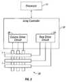
- FIG. 2is a system block diagram illustrating one embodiment of an electronic device incorporating a 3 ⁇ 3 interferometric modulator display.
- FIG. 3is a diagram of movable mirror position versus applied voltage for one exemplary embodiment of an interferometric modulator of FIG. 1 .
- FIG. 4is an illustration of a set of row and column voltages that may be used to drive an interferometric modulator display.
- FIGS. 5A and 5Billustrate one exemplary timing diagram for row and column signals that may be used to write a frame of display data to the 3 ⁇ 3 interferometric modulator display of FIG. 2 .
- FIG. 6Ais a cross section of the device of FIG. 1 .
- FIG. 6Bis a cross section of an alternative embodiment of an interferometric modulator.
- FIG. 6Cis a cross section of another alternative embodiment of an interferometric modulator.
- FIG. 7is a partial schematic diagram of one embodiment of a bi-stable display device, such as an interferometric modulator display incorporating tri-state buffers in the driver circuit.
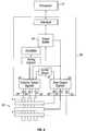
- FIG. 8illustrates the system of FIG. 2 incorporating tri-state isolating buffers.
- FIG. 9is a flowchart illustrating a process of operating a display incorporating tri-state buffers in the driver circuit.
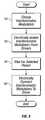
- FIG. 10is a schematic/block diagram of one embodiment of a state sensing circuit.
- FIG. 11is graph illustrating a voltage vs. time response to a voltage pulse for an inteferometric modulator.
- FIG. 12is a schematic/block diagram of another embodiment of a state sensing circuit.
- FIG. 13is graph illustrating a current vs. time response to a voltage pulse for an inteferometric modulator.
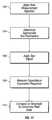
- FIG. 14is a flow chart of a state sensing process.
- FIG. 15is a timing diagram illustrating row and column voltages for setting and testing a row of interferometric modulators.
- FIG. 16is a block diagram of a state sensing apparatus for modulators embedded in arrays.
- FIG. 17is a flow chart of another embodiment of a state sensing process.
- An exemplary array of MEMS interferometric modulatorsare arranged at intersections of rows and columns of electrodes.
- the column electrodehas a lower electrical resistance than the row electrode.
- a driving circuitapplies a potential difference of a first polarity across the column and row electrodes during a first phase and then quickly transition to applying a bias voltage having a polarity opposite to the first polarity during a second phase. More specifically, the driving circuit applies a first voltage to the row electrode during the first phase and a second voltage to the row electrode during the second phase. The driving circuit applies a third voltage to the column electrode during the first phase and a fourth voltage to the column electrode during the second phase.
- the transition between the first phase and the second phasepreferably occurs quickly because the polarity of the voltage across the row and column electrodes is swinging from a positive voltage in one direction to a negative voltage in the opposite direction.
- the voltage swinghappens fast enough that an actuated pixel located at the intersection of the row and column electrodes experiences this polarity reversal does not release as the potential across the pixel passes through zero on its way to the other hysteresis window.
- an absolute value of the difference between the voltages applied to the row electrodeis less than an absolute value of the difference between the voltages applied to the column electrode.
- the following detailed descriptionis directed to certain specific embodiments of the invention. However, the invention can be embodied in a multitude of different ways. In this description, reference is made to the drawings wherein like parts are designated with like numerals throughout. As will be apparent from the following description, the invention may be implemented in any device that is configured to display an image, whether in motion (e.g., video) or stationary (e.g., still image), and whether textual or pictorial.
- motione.g., video
- stationarye.g., still image
- the inventionmay be implemented in or associated with a variety of electronic devices such as, but not limited to, mobile telephones, wireless devices, personal data assistants (PDAs), hand-held or portable computers, GPS receivers/navigators, cameras, MP3 players, camcorders, game consoles, wrist watches, clocks, calculators, television monitors, flat panel displays, computer monitors, auto displays (e.g., odometer display, etc.), cockpit controls and/or displays, display of camera views (e.g., display of a rear view camera in a vehicle), electronic photographs, electronic billboards or signs, projectors, architectural structures, packaging, and aesthetic structures (e.g., display of images on a piece of jewelry).
- MEMS devices of similar structure to those described hereincan also be used in non-display applications such as in electronic switching devices.
- FIG. 1One interferometric modulator display embodiment comprising an interferometric MEMS display element is illustrated in FIG. 1 .
- the pixelsare in either a bright or dark state.
- the display elementIn the bright (“on” or “open”) state, the display element reflects a large portion of incident visible light to a user.
- the dark (“off” or “closed”) stateWhen in the dark (“off” or “closed”) state, the display element reflects little incident visible light to the user.
- the light reflectance properties of the “on” and “off” statesmay be reversed.
- MEMS pixelscan be configured to reflect predominantly at selected colors, allowing for a color display in addition to black and white.
- FIG. 1is an isometric view depicting two adjacent pixels in a series of pixels of a visual display, wherein each pixel comprises a MEMS interferometric modulator.
- an interferometric modulator displaycomprises a row/column array of these interferometric modulators.
- Each interferometric modulatorincludes a pair of reflective layers positioned at a variable and controllable distance from each other to form a resonant optical cavity with at least one variable dimension.
- one of the reflective layersmay be moved between two positions. In the first position, referred to herein as the released state, the movable layer is positioned at a relatively large distance from a fixed partially reflective layer.
- the movable layerIn the second position, the movable layer is positioned more closely adjacent to the partially reflective layer. Incident light that reflects from the two layers interferes constructively or destructively depending on the position of the movable reflective layer, producing either an overall reflective or non-reflective state for each pixel.
- the depicted portion of the pixel array in FIG. 1includes two adjacent interferometric modulators 12 a and 12 b .
- a movable and highly reflective layer 14 ais illustrated in a released position at a predetermined distance from a fixed partially reflective layer 16 a .
- the movable highly reflective layer 14 bis illustrated in an actuated position adjacent to the fixed partially reflective layer 16 b.
- the fixed layers 16 a , 16 bare electrically conductive, partially transparent and partially reflective, and may be fabricated, for example, by depositing one or more layers each of chromium and indium-tin-oxide onto a transparent substrate 20 .
- the layersare patterned into parallel strips, and may form row electrodes in a display device as described further below.
- the movable layers 14 a , 14 bmay be formed as a series of parallel strips of a deposited metal layer or layers (orthogonal to the row electrodes 16 a , 16 b ) deposited on top of posts 18 and an intervening sacrificial material deposited between the posts 18 .
- the deformable metal layersare separated from the fixed metal layers by a defined air gap 19 .
- a highly conductive and reflective materialsuch as aluminum may be used for the deformable layers, and these strips may form column electrodes in a display device.
- the cavity 19remains between the layers 14 a , 16 a and the deformable layer is in a mechanically relaxed state as illustrated by the pixel 12 a in FIG. 1 .
- the capacitor formed at the intersection of the row and column electrodes at the corresponding pixelbecomes charged, and electrostatic forces pull the electrodes together.
- the movable layeris deformed and is forced against the fixed layer (a dielectric material which is not illustrated in this Figure may be deposited on the fixed layer to prevent shorting and control the separation distance) as illustrated by the pixel 12 b on the right in FIG. 1 .
- the behavioris the same regardless of the polarity of the applied potential difference. In this way, row/column actuation that can control the reflective vs. non-reflective pixel states is analogous in many ways to that used in conventional LCD and other display technologies.
- FIGS. 2 through 5illustrate one exemplary process and system for using an array of interferometric modulators in a display application.
- FIG. 2is a system block diagram illustrating one embodiment of an electronic device that may incorporate aspects of the invention.
- the electronic deviceincludes a processor 21 which may be any general purpose single-or multi-chip microprocessor such as an ARM, Pentium®, Pentium II®, Pentium III®, Pentium IV®, Pentium® Pro, an 8051, a MIPS®, a Power PC®, an ALPHA®, or any special purpose microprocessor such as a digital signal processor, microcontroller, or a programmable gate array.
- the processor 21may be configured to execute one or more software modules.
- the processormay be configured to execute one or more software applications, including a web browser, a telephone application, an email program, or any other software application.
- the processor 21is also configured to communicate with an array controller 22 .
- the array controller 22includes a row driver circuit 24 and a column driver circuit 26 that provide signals to a pixel array 30 .
- the row driver circuit 24 and the column driver circuit 26are combined into a driving circuit which applies voltages to both the movable layers 14 and the fixed layers 16 of the array.
- the row/column actuation protocolmay take advantage of a hysteresis property of these devices illustrated in FIG. 3 . It may require, for example, a 10 volt potential difference to cause a movable layer to deform from the released state to the actuated state. However, when the voltage is reduced from that value, the movable layer maintains its state as the voltage drops back below 10 volts. In the exemplary embodiment of FIG. 3 , the movable layer does not release completely until the voltage drops below 2 volts. There is thus a range of voltage, about 3 to 7 V in the example illustrated in FIG.
- the row/column actuation protocolcan be designed such that during row strobing, pixels in the strobed row that are to be actuated are exposed to a voltage difference of about 10 volts, and pixels that are to be released are exposed to a voltage difference of close to zero volts. After the strobe, the pixels are exposed to a steady state voltage difference of about 5 volts such that they remain in whatever state the row strobe put them in.
- each pixelsees a potential difference within the “stability window” of 3-7 volts in this example.
- This featuremakes the pixel design illustrated in FIG. 1 stable under the same applied voltage conditions in either an actuated or released pre-existing state. Since each pixel of the interferometric modulator, whether in the actuated or released state, is essentially a capacitor formed by the fixed and moving reflective layers, this stable state can be held at a voltage within the hysteresis window with almost no power dissipation. Essentially no current flows into the pixel if the applied potential is fixed.
- a display framemay be created by asserting the set of column electrodes in accordance with the desired set of actuated pixels in the first row.
- a row pulseis then applied to the row 1 electrode, actuating the pixels corresponding to the asserted column lines.
- the asserted set of column electrodesis then changed to correspond to the desired set of actuated pixels in the second row.
- a pulseis then applied to the row 2 electrode, actuating the appropriate pixels in row 2 in accordance with the asserted column electrodes.
- the row 1 pixelsare unaffected by the row 2 pulse, and remain in the state they were set to during the row 1 pulse. This may be repeated for the entire series of rows in a sequential fashion to produce the frame.
- the framesare refreshed and/or updated with new display data by continually repeating this process at some desired number of frames per second.
- protocols for driving row and column electrodes of pixel arrays to produce display framesare also well known and may be used in conjunction with the present invention.
- FIGS. 4 and 5illustrate one possible actuation protocol for creating a display frame on the 3 ⁇ 3 array of FIG. 2 .
- FIG. 4illustrates a possible set of column and row voltage levels that may be used for pixels exhibiting the hysteresis curves of FIG. 3 .
- actuating a pixelinvolves setting the appropriate column to ⁇ V bias , and the appropriate row to + ⁇ V, which may correspond to ⁇ 5 volts and +5 volts respectively Releasing the pixel is accomplished by setting the appropriate column to +V bias , and the appropriate row to the same + ⁇ V, producing a zero volt potential difference across the pixel.
- the pixelsare stable in whatever state they were originally in, regardless of whether the column is at +V bias , or ⁇ V bias .
- voltages of opposite polarity than those described abovecan be used, e.g., actuating a pixel can involve setting the appropriate column to +V bias , and the appropriate row to ⁇ V.
- releasing the pixelis accomplished by setting the appropriate column to ⁇ V bias , and the appropriate row to the same ⁇ V, producing a zero volt potential difference across the pixel.
- FIG. 5Bis a timing diagram showing a series of row and column signals applied to the 3 ⁇ 3 array of FIG. 2 which will result in the display arrangement illustrated in FIG. 5A , where actuated pixels are non-reflective.
- the pixelsPrior to writing the frame illustrated in FIG. 5A , the pixels can be in any state, and in this example, all the rows are at 0 volts, and all the columns are at +5 volts. With these applied voltages, all pixels are stable in their existing actuated or released states.
- pixels ( 1 , 1 ), ( 1 , 2 ), ( 2 , 2 ), ( 3 , 2 ) and ( 3 , 3 )are actuated.
- columns 1 and 2are set to ⁇ 5 volts
- column 3is set to +5 volts. This does not change the state of any pixels, because all the pixels remain in the 3-7 volt stability window.
- Row 1is then strobed with a pulse that goes from 0, up to 5 volts, and back to zero. This actuates the ( 1 , 1 ) and ( 1 , 2 ) pixels and releases the ( 1 , 3 ) pixel. No other pixels in the array are affected.
- row 2is set to ⁇ 5 volts, and columns 1 and 3 are set to +5 volts.
- the same strobe applied to row 2will then actuate pixel ( 2 , 2 ) and release pixels ( 2 , 1 ) and ( 2 , 3 ). Again, no other pixels of the array are affected.
- Row 3is similarly set by setting columns 2 and 3 to ⁇ 5 volts, and column 1 to +5 volts.
- the row 3strobe sets the row 3 pixels as shown in FIG. 5A . After writing the frame, the row potentials are zero, and the column potentials can remain at either +5 or ⁇ 5 volts, and the display is then stable in the arrangement of FIG. 5A .
- FIGS. 6A-6Cillustrate three different embodiments of the moving mirror structure.
- FIG. 6Ais a cross section of the embodiment of FIG. 1 , where a strip of metal material 14 is deposited on orthogonally extending supports 18 .
- the moveable reflective material 14is attached to supports at the corners only, on tethers 32 .
- the moveable reflective material 14is suspended from a deformable layer 34 .
- This embodimenthas benefits because the structural design and materials used for the reflective material 14 can be optimized with respect to the optical properties, and the structural design and materials used for the deformable layer 34 can be optimized with respect to desired mechanical properties.
- the column voltagesswing between +5 volts and ⁇ 5 volts between phases of the writing process.
- the driving circuitapplies +5 volts to the column electrode.
- the driving circuitapplies ⁇ 5 volts to the column electrode.
- the polarity reversalshould happen significantly faster than the mechanical response time of an actuated pixel.
- the deformed reflective layerwill stay deformed long enough for the voltage to swing back to the 5 V bias voltage, where the electrostatic force returns and continues to hold the pixel in the actuated state.
- the necessary speedis much easier to accomplish if the electrode to which these voltage swings are applied has a low electrical resistance.
- a low electrical resistanceminimizes the RC charging time constant of the pixels, and allows the voltage across each pixel to swing rapidly in response to the drive potentials applied by the driving circuit.
- one set of electrodesmay be fabricated from chromium and indium-tin-oxide, and the other from aluminum.
- the aluminum electrodeshave a much lower resistance than the chrome/ITO electrodes. It is therefore advantageous to apply any polarity reversing swings of potential to the aluminum electrodes rather than to the chrome/ITO electrodes.
- the deformable aluminum layersare used as the column electrodes because they receive these rapid voltage swings from the driving circuit between phases.
- the row electrodesmay be subject to polarity reversing voltage swings. In these embodiment, the low resistance layer would be attached to the row driver.
- the inventioncomprises an array of MEMS devices at the intersections of a set of row electrodes and a set of column electrodes.
- One of the set of row electrodes or set of column electrodeshas a lower electrical resistance than the other.
- a row drive circuitis connected to the row electrodes, and a column drive circuit is connected to the column electrodes.
- the row drive circuit and the column drive circuitare combined in a single driving circuit. Outputs from the driving circuit are connected to the row electrode and the column electrode.
- the MEMS devicesare driven with voltage signals applied to the row and column electrodes.
- the set of voltages applied to one of the set of row electrodes or the set of column electrodesincludes voltage swings that cause the polarity and magnitude of the voltage across at least some of the MEMS devices to swing from a stable bias potential of one polarity to a stable bias potential of the opposite polarity.
- the set of electrodes with the lower resistanceis coupled to the set of voltages that includes voltage swings that cause the polarity and magnitude of the voltage across at least some of the MEMS devices to swing from a stable bias potential of one polarity to a stable bias potential of the opposite polarity.
- the driving circuitapplies a potential difference of a first polarity across at least one MEMS device during a first phase and then quickly transitions to applying a bias voltage having a polarity opposite to the first polarity across the at least one MEMS device during a second phase. More specifically during the first phase, the driving circuit applies a first voltage to a first electrode and a third voltage to a second electrode having a lower electrical resistance than the first electrode. The first and third voltages together form the potential difference of the first polarity across the at least MEMS device the first phase.
- the driving circuitapplies a second voltage to the first electrode and a fourth voltage to the second electrode.
- the second and fourth voltagesform the bias voltage having the polarity opposite to the first polarity across the at least MEMS device the second phase.
- an absolute value of the difference between the first and second voltagesbeing less than an absolute value of the difference between the third and fourth voltages, the second electrode which has the lower electrical resistance experiences higher voltage swings than the first electrode.
- the first voltageis substantially equal to the second voltage and is between the third voltage and the fourth voltage.
- the first and second voltagesare zero and the third and fourth voltages are ⁇ 5 volts and +5 volts, respectively.
- two times a 5 volt bias voltageis substantially equal to the absolute value of the difference between the third voltage and the fourth voltage.
- FIG. 7is a partial schematic diagram of one embodiment of a MEMS array such as an interferometric modulator display array as described above.
- the elements of the arrayare stable in either the actuated state or the released state if an appropriate bias voltage is applied across the electrodes.
- the elementsare stable if the rows are at +5 V, and the columns are anywhere between ⁇ 2 and +2 volts.
- the driver circuitincludes a plurality of tri-state buffers 50 provided on each of the columns and each of the rows of array. Each of the tri-state buffers 50 are connected to a hold-mode select line from the array controller 22 .
- the charge pumps and analog circuitry in the array controllercan be cycled into the off state during a significant fraction of the total display operation time, significantly reducing power consumption. This cycling can occur during maintenance of a display of a static frame, between row strobes during the write process, etc.
- FIG. 8shows the array controller of FIG. 2 comprising a plurality of tri-state buffers 50 .
- the plurality of tri-state buffers 50are advantageously provided on each of the columns and each of the rows of array 30 .
- the tri-state buffers 50are connected to hold-mode signals which open the connection between the respective row or column of the array when they are asserted. When the hold-mode select lines are asserted, lines from the driver to the array are opened, substantially eliminating any leakage path for the charge stored on each pixel capacitance. The pixels are thus held in the previously charged or discharged state without any driver input, until the charge slowly dissipates, either through leakage across the pixel or through a non-infinite tri-state open resistance.
- the open or closed state of the rows and columnscan be individually controlled as desired.
- any controllable series switchsuch as a series FET could be used to implement this display/driver decoupling.
- the array controller 22may also include a boost circuit 42 for converting control signals to a voltage sufficient for driving the array 30 .
- the array controller 22also includes a frame buffer 44 .
- the frame buffer 44typically includes sufficient memory to store the current displayed frame for refresh purposes.
- Portions of the array controller 22 as well as additional circuitry and functionalitymay be provided by a graphics controller which is typically connected between the actual display drivers and a general purpose microprocessor. Exemplary embodiments of the graphics controller include 69030 or 69455 controllers from Chips and Technology, Inc., the S1D1300 series from Seiko Epson, and the Solomon Systech 1906.
- FIG. 9is a flowchart illustrating an exemplary process operating the display of FIG. 7 or 8 .
- activating a plurality of tri-state buffers 50the state of the interferometric modulators may be maintained with low power dissipation.
- additional stepscan be added, others removed, and the sequence of steps rearranged to the steps shown in FIG. 9 .
- each of the interferometric modulators in the pixelsare charged.
- the bias voltage used prior to disconnecting the arrayis increased to be closer to the actuation voltage, rather than right in the middle of the hysteresis window.
- the row voltagescould be +5 volts
- the column voltagescould be set to ⁇ 2 volts, rather than 0 volts.
- the interferometric modulatorsare charged proximate to but not higher than the actuation voltage for the respective interferometric modulators, e.g., 75%, 90%, or 95%, of the actuation voltage.
- the pixelsare highly charged but the voltage differential for any of interferometric modulators should not cause a change in state for any of the released elements of the array.
- the interferometric modulatorsare electrically isolated from the array controller 22 .
- the tri-state buffers 50are activated so as to cut the lines from the array controller 22 to the array elements.
- the array controller 22powers down at least a portion of its power consuming circuitry and waits for a selected period which will depend on the RC time constant of the circuit with the tri-state buffer open.
- capacitance valueswill be in the picofarad range, and the resistance in the 1000 Mohm range, putting the time constant in the millisecond range.
- the duration of the off periodis about 1 to 10 msec.
- Other exemplary time durationsinclude at least 0.5 seconds and at least two seconds for high capacitance arrays.
- the selected periodis user-definable.
- the interferometric modulatorsare reconnected to the array controller 22 .
- the process of FIG. 9is repeated during the course of image display and modification.
- the state of a pixelcan be determined by taking advantage of the fact that the capacitance across the pixel mirrors is much larger, often about ten times larger, when the pixels are in the actuated state than when they are in the released state.
- This pixel capacitance valuecan be sensed in a variety of ways by sensing capacitance dependent electrical properties of the pixel, some of which are described in more detail below.
- FIG. 10After pixel writing, whether the whole frame is complete or prior to that time, all the column tri-state buffers can be placed in the open (decoupled) configuration except one column containing the pixel to be tested.
- the row driverthen applies a low amplitude pulse to the row electrode containing the pixel to be tested, which charges up in response to the increased voltage.
- FIG. 11the voltage across the pixel will increase in response to this applied voltage in accordance with the RC time constant ( ⁇ ) of the circuit.
- the capacitanceis the capacitance of the pixel 61
- the resistance of the circuitmay include the row driver output impedance and/or any filter resistor 62 that might be placed in series with the row electrode.
- the voltage at the test point 63 when the pixel 61 is in a low capacitance state (e.g. in the released state)will increase faster as illustrated by curve 60 than when the pixel 61 is in a high capacitance state (e.g. in the actuated state) as illustrated by curve 69 . If the voltage across the pixel is determined at a certain time during this charging period, at ⁇ /3 for example, the state of the pixel can be determined. This voltage can be detected and measured by a voltage sensing circuit 64 .
- a pulse having a duration of ⁇ /3is applied to the pixel, the voltage across the pixel will increase and decrease as shown in the trace 66 (also shown in FIG. 11 ). If this signal is applied to the input of a comparator 68 with V thresh applied to the negative input, a pulse will be output from the comparator only if the voltage across the pixel exceeded V thresh at some time during the pulse, where V thresh is defined as shown in FIG. 11 .
- the output of the comparator 68can be latched to produce an indication of whether that pixel is actuated (latch low) or released (latch high).
- FIGS. 12 and 13illustrate an alternative method of detecting pixel state.
- a current sensing circuit 70is used rather than a voltage sensing circuit.
- a voltage pulseis applied as above, which causes a current pulse as the pixel capacitance charges. As illustrated in FIG. 13 , this current pulse decays slower (curve 75 ) for a larger capacitance of pixel 61 than for a smaller capacitance (curve 77 ).
- the current pulsecan be converted to a voltage pulse by measuring the voltage across a series resistance 72 in the column line (amplifiers configured as current to voltage converters could also be used). The voltage across the resistor can be sensed by an amplifier configured as an integrator 74 illustrated in FIG. 12 .
- the output of the integratorcan be routed to a similar comparator 76 and latch as is FIG. 10 .
- the comparator 76will only produce an output pulse if the current pulse through the circuit is sufficient (given the value of the resistor 72 and the time constant/amplification of the integrator 74 ) to produce a voltage at the comparator input greater than a threshold voltage V thresh2 shown in FIG. 12 .
- FIG. 12shows a switch 78 used to switch resistance 72 into the column line, but it will be appreciated that this would not be necessary if a suitable filter resistor, for example, was already present.
- FIG. 14is a flowchart illustrating an exemplary process for determining an open or closed state of an interferometric modulator.
- a test pulseis applied to the pixel at step 80 .
- a capacitance dependent response to the pulseis measured.
- the responseis compared to a threshold to determine the state of the pixel.
- Pixel state sensingcan be advantageous for a variety of reasons. For example, on the next frame update or refresh, only those pixels that are different from the next desired frame need be updated. For a static display, the pixel states may be monitored to detect which pixels have relaxed from an actuated state to a released state due to charge leakage. Selective updating could be performed in a variety of ways. For example, once one or more pixels change from the desired state, the driver circuitry could be turned back on, the tri-state buffers closed, and row strobing could be limited to only those rows which include pixels in an undesired state. Other rows could be skipped. This reduces the total energy required to update the display. Pixel state sensing could also be advantageous during the frame writing process, because as rows of pixels are written, they could be checked to determine if they were written correctly or not. If not, the row could be written again until correct.
- FIG. 15An implementation of this last process is illustrated in FIG. 15 .
- a row 1 test time 92is entered.
- row 1 and column 1are connected to the drive circuitry, and a test pulse 94 of about 1 volt or less is applied to row 1 .
- the capacitance dependent response of pixel ( 1 , 1 )is monitored to be sure it is in the actuated state as shown in FIG. 5A . This is repeated for pixels ( 1 , 2 ) and ( 1 , 3 ) during subsequent portions of the row 1 test time.
- the systemthen enters the row 2 line time, or alternatively, repeats the row 1 line time if it is determined that one or more pixels in row 1 have not been correctly written.
- the test time periodis shown much longer than would normally be necessary, as the pulse time periods for testing can be very short compared to the pulse periods used to actuate the pixels during the write process.
- the testing processmay be somewhat more complex. This is because the test pulse is applied to an entire row of pixels.
- the time constant of the charging processis dependent on the capacitance between the entire row electrode and the return column electrode, and this can be affected by the relative states of all the pixels in the row, not just on the state of the pixel being tested 61 , shown again in FIG. 16 .
- the dominant factor in the capacitancewill be the state of the pixel being tested, but since there may be hundreds of pixels in the row, the combined effect of the remainder can be significant.
- This determinationcan be done in several ways.
- One embodimentcan include in each row, at the end of the row outside the viewed area of the display, a test pixel 98 .
- This pixelcan be switched between states, and the rise times for the test pulse can be determined for both the actuated and released states. In this way, the time period having the maximum voltage difference between states, and the voltage values between which V thresh should be located between could be determined based on the test pixel response. These values could then be used to test the state of the other pixels in the row.
- a filter resistorcould be placed at the end of the row instead of a test pixel.
- a collective capacitance measurement for the whole row electrodecould then be made.
- the drive control circuitrycould use this information to compute or look up an appropriate value for ⁇ /3, V thresh , or both, to test the pixels in that row.
- FIG. 17A general state sensing process using these principles for pixels embedded in arrays of rows and columns is illustrated in FIG. 17 .
- row measurement signalsare applied to a row containing a pixel to be sensed. These signals could involve testing a test pixel or an overall row capacitance measurement as described above.
- appropriate test parameterssuch as period ⁇ /3 and/or V thresh are determined for later pixel testing in the row.
- a test pulseis then applied to the row at step 106 .
- a capacitance dependent response to the pulseis measured.
- the responseis compared to a threshold to determine the state of a selected pixel in the row.
- Pulse amplitudes and durations for the pixel state sensing processmay be selected based on a variety of desired factors.
- the pulsemay be shaped to control the total charge injected into the row.
- the pulse current and time profilecan be defined such that a pre-selected charge is injected into the pixel regardless of its capacitance value. In this case, the resulting voltage across the pixel will be inversely proportional to the pixel capacitance. It may be possible to use this method for pixels in an array as well, but its usefulness may be limited since the charge injected into the row may be distributed throughout the hundreds of row pixels in a way that is complicated and difficult to predict.
- Pulse durationsmay be selected based on the circuit ⁇ value, with short pulses preferred for time savings.
- the driverwill advantageously supply the appropriate bias voltage when not applying a charging pulse and when not decoupled by the tri-state amplifiers, and will generate pulses deviating from this bias voltage that are small enough (e.g. no more than 1 or 2 volts typically) such that the applied pixel voltages are never outside of the hysteresis window.
Landscapes
- Physics & Mathematics (AREA)
- General Physics & Mathematics (AREA)
- Engineering & Computer Science (AREA)
- Spectroscopy & Molecular Physics (AREA)
- Optics & Photonics (AREA)
- Computer Hardware Design (AREA)
- Theoretical Computer Science (AREA)
- Mechanical Light Control Or Optical Switches (AREA)
- Control Of Indicators Other Than Cathode Ray Tubes (AREA)
- Micromachines (AREA)
Abstract
Description
Claims (22)
Priority Applications (1)
| Application Number | Priority Date | Filing Date | Title |
|---|---|---|---|
| US11/511,908US7928940B2 (en) | 2004-08-27 | 2006-08-28 | Drive method for MEMS devices |
Applications Claiming Priority (8)
| Application Number | Priority Date | Filing Date | Title |
|---|---|---|---|
| US60489304P | 2004-08-27 | 2004-08-27 | |
| US60489204P | 2004-08-27 | 2004-08-27 | |
| US61403204P | 2004-09-27 | 2004-09-27 | |
| US2769304A | 2004-12-30 | 2004-12-30 | |
| US2655504A | 2004-12-30 | 2004-12-30 | |
| US64605305P | 2005-01-21 | 2005-01-21 | |
| US11/118,612US7889163B2 (en) | 2004-08-27 | 2005-04-29 | Drive method for MEMS devices |
| US11/511,908US7928940B2 (en) | 2004-08-27 | 2006-08-28 | Drive method for MEMS devices |
Related Parent Applications (1)
| Application Number | Title | Priority Date | Filing Date |
|---|---|---|---|
| US11/118,612ContinuationUS7889163B2 (en) | 2004-08-27 | 2005-04-29 | Drive method for MEMS devices |
Publications (2)
| Publication Number | Publication Date |
|---|---|
| US20070024550A1 US20070024550A1 (en) | 2007-02-01 |
| US7928940B2true US7928940B2 (en) | 2011-04-19 |
Family
ID=35466612
Family Applications (3)
| Application Number | Title | Priority Date | Filing Date |
|---|---|---|---|
| US11/118,612Expired - Fee RelatedUS7889163B2 (en) | 2004-08-27 | 2005-04-29 | Drive method for MEMS devices |
| US11/511,908Expired - Fee RelatedUS7928940B2 (en) | 2004-08-27 | 2006-08-28 | Drive method for MEMS devices |
| US12/985,228AbandonedUS20110096056A1 (en) | 2004-08-27 | 2011-01-05 | Drive method for mems devices |
Family Applications Before (1)
| Application Number | Title | Priority Date | Filing Date |
|---|---|---|---|
| US11/118,612Expired - Fee RelatedUS7889163B2 (en) | 2004-08-27 | 2005-04-29 | Drive method for MEMS devices |
Family Applications After (1)
| Application Number | Title | Priority Date | Filing Date |
|---|---|---|---|
| US12/985,228AbandonedUS20110096056A1 (en) | 2004-08-27 | 2011-01-05 | Drive method for mems devices |
Country Status (8)
| Country | Link |
|---|---|
| US (3) | US7889163B2 (en) |
| EP (1) | EP1789947A2 (en) |
| CN (1) | CN102214447A (en) |
| AU (1) | AU2005280271A1 (en) |
| BR (1) | BRPI0514655A (en) |
| IL (1) | IL180970A0 (en) |
| TW (1) | TWI375657B (en) |
| WO (1) | WO2006026227A2 (en) |
Cited By (1)
| Publication number | Priority date | Publication date | Assignee | Title |
|---|---|---|---|---|
| US20110043960A1 (en)* | 2009-08-20 | 2011-02-24 | Kabushiki Kaisha Toshiba | Programmable actuator and programming method thereof |
Families Citing this family (124)
| Publication number | Priority date | Publication date | Assignee | Title |
|---|---|---|---|---|
| US7471444B2 (en)* | 1996-12-19 | 2008-12-30 | Idc, Llc | Interferometric modulation of radiation |
| US8928967B2 (en) | 1998-04-08 | 2015-01-06 | Qualcomm Mems Technologies, Inc. | Method and device for modulating light |
| WO1999052006A2 (en) | 1998-04-08 | 1999-10-14 | Etalon, Inc. | Interferometric modulation of radiation |
| TWI289708B (en) | 2002-12-25 | 2007-11-11 | Qualcomm Mems Technologies Inc | Optical interference type color display |
| US7417782B2 (en) | 2005-02-23 | 2008-08-26 | Pixtronix, Incorporated | Methods and apparatus for spatial light modulation |
| US20070002009A1 (en)* | 2003-10-07 | 2007-01-04 | Pasch Nicholas F | Micro-electromechanical display backplane and improvements thereof |
| US7342705B2 (en) | 2004-02-03 | 2008-03-11 | Idc, Llc | Spatial light modulator with integrated optical compensation structure |
| US7889163B2 (en)* | 2004-08-27 | 2011-02-15 | Qualcomm Mems Technologies, Inc. | Drive method for MEMS devices |
| US7499208B2 (en)* | 2004-08-27 | 2009-03-03 | Udc, Llc | Current mode display driver circuit realization feature |
| US7560299B2 (en)* | 2004-08-27 | 2009-07-14 | Idc, Llc | Systems and methods of actuating MEMS display elements |
| US7551159B2 (en) | 2004-08-27 | 2009-06-23 | Idc, Llc | System and method of sensing actuation and release voltages of an interferometric modulator |
| US7515147B2 (en)* | 2004-08-27 | 2009-04-07 | Idc, Llc | Staggered column drive circuit systems and methods |
| US8878825B2 (en)* | 2004-09-27 | 2014-11-04 | Qualcomm Mems Technologies, Inc. | System and method for providing a variable refresh rate of an interferometric modulator display |
| US7136213B2 (en)* | 2004-09-27 | 2006-11-14 | Idc, Llc | Interferometric modulators having charge persistence |
| US7310179B2 (en)* | 2004-09-27 | 2007-12-18 | Idc, Llc | Method and device for selective adjustment of hysteresis window |
| TWI259424B (en)* | 2004-09-27 | 2006-08-01 | Au Optronics Corp | Method and device for adjusting driving voltage of microelectromechanical optical device and display using the same |
| AU2005289445A1 (en) | 2004-09-27 | 2006-04-06 | Idc, Llc | Method and device for multistate interferometric light modulation |
| US7345805B2 (en)* | 2004-09-27 | 2008-03-18 | Idc, Llc | Interferometric modulator array with integrated MEMS electrical switches |
| US7626581B2 (en)* | 2004-09-27 | 2009-12-01 | Idc, Llc | Device and method for display memory using manipulation of mechanical response |
| US8310441B2 (en) | 2004-09-27 | 2012-11-13 | Qualcomm Mems Technologies, Inc. | Method and system for writing data to MEMS display elements |
| US7724993B2 (en)* | 2004-09-27 | 2010-05-25 | Qualcomm Mems Technologies, Inc. | MEMS switches with deforming membranes |
| US7675669B2 (en)* | 2004-09-27 | 2010-03-09 | Qualcomm Mems Technologies, Inc. | Method and system for driving interferometric modulators |
| US7545550B2 (en)* | 2004-09-27 | 2009-06-09 | Idc, Llc | Systems and methods of actuating MEMS display elements |
| US20060066594A1 (en)* | 2004-09-27 | 2006-03-30 | Karen Tyger | Systems and methods for driving a bi-stable display element |
| US7532195B2 (en)* | 2004-09-27 | 2009-05-12 | Idc, Llc | Method and system for reducing power consumption in a display |
| US7446927B2 (en)* | 2004-09-27 | 2008-11-04 | Idc, Llc | MEMS switch with set and latch electrodes |
| US7843410B2 (en)* | 2004-09-27 | 2010-11-30 | Qualcomm Mems Technologies, Inc. | Method and device for electrically programmable display |
| US7679627B2 (en)* | 2004-09-27 | 2010-03-16 | Qualcomm Mems Technologies, Inc. | Controller and driver features for bi-stable display |
| US7304786B2 (en) | 2005-02-23 | 2007-12-04 | Pixtronix, Inc. | Methods and apparatus for bi-stable actuation of displays |
| US20070205969A1 (en) | 2005-02-23 | 2007-09-06 | Pixtronix, Incorporated | Direct-view MEMS display devices and methods for generating images thereon |
| US7271945B2 (en) | 2005-02-23 | 2007-09-18 | Pixtronix, Inc. | Methods and apparatus for actuating displays |
| US8519945B2 (en) | 2006-01-06 | 2013-08-27 | Pixtronix, Inc. | Circuits for controlling display apparatus |
| US9087486B2 (en) | 2005-02-23 | 2015-07-21 | Pixtronix, Inc. | Circuits for controlling display apparatus |
| US9261694B2 (en) | 2005-02-23 | 2016-02-16 | Pixtronix, Inc. | Display apparatus and methods for manufacture thereof |
| US7405852B2 (en) | 2005-02-23 | 2008-07-29 | Pixtronix, Inc. | Display apparatus and methods for manufacture thereof |
| US7746529B2 (en) | 2005-02-23 | 2010-06-29 | Pixtronix, Inc. | MEMS display apparatus |
| US7502159B2 (en) | 2005-02-23 | 2009-03-10 | Pixtronix, Inc. | Methods and apparatus for actuating displays |
| US8159428B2 (en) | 2005-02-23 | 2012-04-17 | Pixtronix, Inc. | Display methods and apparatus |
| US9229222B2 (en) | 2005-02-23 | 2016-01-05 | Pixtronix, Inc. | Alignment methods in fluid-filled MEMS displays |
| US7675665B2 (en) | 2005-02-23 | 2010-03-09 | Pixtronix, Incorporated | Methods and apparatus for actuating displays |
| US8310442B2 (en) | 2005-02-23 | 2012-11-13 | Pixtronix, Inc. | Circuits for controlling display apparatus |
| US9082353B2 (en) | 2010-01-05 | 2015-07-14 | Pixtronix, Inc. | Circuits for controlling display apparatus |
| US7304785B2 (en) | 2005-02-23 | 2007-12-04 | Pixtronix, Inc. | Display methods and apparatus |
| US9158106B2 (en) | 2005-02-23 | 2015-10-13 | Pixtronix, Inc. | Display methods and apparatus |
| US7616368B2 (en)* | 2005-02-23 | 2009-11-10 | Pixtronix, Inc. | Light concentrating reflective display methods and apparatus |
| US8482496B2 (en) | 2006-01-06 | 2013-07-09 | Pixtronix, Inc. | Circuits for controlling MEMS display apparatus on a transparent substrate |
| US7755582B2 (en)* | 2005-02-23 | 2010-07-13 | Pixtronix, Incorporated | Display methods and apparatus |
| US7999994B2 (en) | 2005-02-23 | 2011-08-16 | Pixtronix, Inc. | Display apparatus and methods for manufacture thereof |
| US7742016B2 (en)* | 2005-02-23 | 2010-06-22 | Pixtronix, Incorporated | Display methods and apparatus |
| US7948457B2 (en)* | 2005-05-05 | 2011-05-24 | Qualcomm Mems Technologies, Inc. | Systems and methods of actuating MEMS display elements |
| EP1878001A1 (en)* | 2005-05-05 | 2008-01-16 | QUALCOMM Incorporated, Inc. | Dynamic driver ic and display panel configuration |
| US7920136B2 (en) | 2005-05-05 | 2011-04-05 | Qualcomm Mems Technologies, Inc. | System and method of driving a MEMS display device |
| US7355779B2 (en)* | 2005-09-02 | 2008-04-08 | Idc, Llc | Method and system for driving MEMS display elements |
| US20070126673A1 (en)* | 2005-12-07 | 2007-06-07 | Kostadin Djordjev | Method and system for writing data to MEMS display elements |
| US8391630B2 (en) | 2005-12-22 | 2013-03-05 | Qualcomm Mems Technologies, Inc. | System and method for power reduction when decompressing video streams for interferometric modulator displays |
| US7916980B2 (en) | 2006-01-13 | 2011-03-29 | Qualcomm Mems Technologies, Inc. | Interconnect structure for MEMS device |
| US8194056B2 (en)* | 2006-02-09 | 2012-06-05 | Qualcomm Mems Technologies Inc. | Method and system for writing data to MEMS display elements |
| US8526096B2 (en) | 2006-02-23 | 2013-09-03 | Pixtronix, Inc. | Mechanical light modulators with stressed beams |
| US8049713B2 (en)* | 2006-04-24 | 2011-11-01 | Qualcomm Mems Technologies, Inc. | Power consumption optimized display update |
| US7876489B2 (en) | 2006-06-05 | 2011-01-25 | Pixtronix, Inc. | Display apparatus with optical cavities |
| EP1943555B1 (en) | 2006-10-06 | 2012-05-02 | QUALCOMM MEMS Technologies, Inc. | Optical loss structure integrated in an illumination apparatus of a display |
| EP1943551A2 (en) | 2006-10-06 | 2008-07-16 | Qualcomm Mems Technologies, Inc. | Light guide |
| EP2080045A1 (en) | 2006-10-20 | 2009-07-22 | Pixtronix Inc. | Light guides and backlight systems incorporating light redirectors at varying densities |
| US7556981B2 (en) | 2006-12-29 | 2009-07-07 | Qualcomm Mems Technologies, Inc. | Switches for shorting during MEMS etch release |
| US7852546B2 (en) | 2007-10-19 | 2010-12-14 | Pixtronix, Inc. | Spacers for maintaining display apparatus alignment |
| US9176318B2 (en) | 2007-05-18 | 2015-11-03 | Pixtronix, Inc. | Methods for manufacturing fluid-filled MEMS displays |
| WO2008088892A2 (en)* | 2007-01-19 | 2008-07-24 | Pixtronix, Inc. | Sensor-based feedback for display apparatus |
| EP2067841A1 (en)* | 2007-12-06 | 2009-06-10 | Agfa HealthCare NV | X-Ray imaging photostimulable phosphor screen or panel. |
| US8068710B2 (en)* | 2007-12-07 | 2011-11-29 | Qualcomm Mems Technologies, Inc. | Decoupled holographic film and diffuser |
| EP2252991A1 (en)* | 2008-02-11 | 2010-11-24 | QUALCOMM MEMS Technologies, Inc. | Method and apparatus for sensing, measurement or characterization of display elements integrated with the display drive scheme, and system and applications using the same |
| US20090201282A1 (en)* | 2008-02-11 | 2009-08-13 | Qualcomm Mems Technologies, Inc | Methods of tuning interferometric modulator displays |
| US8395371B2 (en)* | 2008-02-11 | 2013-03-12 | Qualcomm Mems Technologies, Inc. | Methods for characterizing the behavior of microelectromechanical system devices |
| WO2009102620A2 (en)* | 2008-02-11 | 2009-08-20 | Qualcomm Mems Technologies Inc. | Methods for measurement and characterization of interferometric modulators |
| US8466858B2 (en)* | 2008-02-11 | 2013-06-18 | Qualcomm Mems Technologies, Inc. | Sensing to determine pixel state in a passively addressed display array |
| RU2503068C2 (en)* | 2008-02-11 | 2013-12-27 | Квалкомм Мемс Текнолоджис, Инк. | Measurement of electric control parameters of display based on microelectromechanical systems and device for electric measurement of such parameters |
| US7977931B2 (en)* | 2008-03-18 | 2011-07-12 | Qualcomm Mems Technologies, Inc. | Family of current/power-efficient high voltage linear regulator circuit architectures |
| US8248560B2 (en) | 2008-04-18 | 2012-08-21 | Pixtronix, Inc. | Light guides and backlight systems incorporating prismatic structures and light redirectors |
| US7782522B2 (en) | 2008-07-17 | 2010-08-24 | Qualcomm Mems Technologies, Inc. | Encapsulation methods for interferometric modulator and MEMS devices |
| GB0814079D0 (en)* | 2008-08-01 | 2008-09-10 | Liquavista Bv | Electrowetting system |
| US20100045630A1 (en)* | 2008-08-19 | 2010-02-25 | Qualcomm Incorporated | Capacitive MEMS-Based Display with Touch Position Sensing |
| US8169679B2 (en) | 2008-10-27 | 2012-05-01 | Pixtronix, Inc. | MEMS anchors |
| US8736590B2 (en)* | 2009-03-27 | 2014-05-27 | Qualcomm Mems Technologies, Inc. | Low voltage driver scheme for interferometric modulators |
| TWI402737B (en)* | 2009-05-04 | 2013-07-21 | Mitac Int Corp | Multi - touch device and its method |
| US7990604B2 (en) | 2009-06-15 | 2011-08-02 | Qualcomm Mems Technologies, Inc. | Analog interferometric modulator |
| US9090456B2 (en)* | 2009-11-16 | 2015-07-28 | Qualcomm Mems Technologies, Inc. | System and method of manufacturing an electromechanical device by printing raised conductive contours |
| JP5310529B2 (en)* | 2009-12-22 | 2013-10-09 | 株式会社豊田中央研究所 | Oscillator for plate member |
| US8149496B2 (en)* | 2009-12-22 | 2012-04-03 | Qualcomm Mems Technologies, Inc. | Integrated touch for IMOD displays using back glass |
| US8884940B2 (en)* | 2010-01-06 | 2014-11-11 | Qualcomm Mems Technologies, Inc. | Charge pump for producing display driver output |
| US8310421B2 (en)* | 2010-01-06 | 2012-11-13 | Qualcomm Mems Technologies, Inc. | Display drive switch configuration |
| US20110164027A1 (en)* | 2010-01-06 | 2011-07-07 | Qualcomm Mems Technologies, Inc. | Method of detecting change in display data |
| US20110164068A1 (en)* | 2010-01-06 | 2011-07-07 | Qualcomm Mems Technologies, Inc. | Reordering display line updates |
| KR20120132680A (en) | 2010-02-02 | 2012-12-07 | 픽스트로닉스 인코포레이티드 | Methods for manufacturing cold seal fluid-filled display apparatus |
| US9398666B2 (en) | 2010-03-11 | 2016-07-19 | Pixtronix, Inc. | Reflective and transflective operation modes for a display device |
| WO2011112861A1 (en)* | 2010-03-12 | 2011-09-15 | Qualcomm Mems Technologies, Inc. | Line multiplying to enable increased refresh rate of a display |
| US8659611B2 (en)* | 2010-03-17 | 2014-02-25 | Qualcomm Mems Technologies, Inc. | System and method for frame buffer storage and retrieval in alternating orientations |
| US20110316832A1 (en)* | 2010-06-24 | 2011-12-29 | Qualcomm Mems Technologies, Inc. | Pixel drive scheme having improved release characteristics |
| JP2013541041A (en)* | 2010-09-03 | 2013-11-07 | クォルコム・メムズ・テクノロジーズ・インコーポレーテッド | System and method for compensating for leakage current when sensing the state of a display element |
| US8294184B2 (en) | 2011-02-23 | 2012-10-23 | Qualcomm Mems Technologies, Inc. | EMS tunable transistor |
| US8780104B2 (en) | 2011-03-15 | 2014-07-15 | Qualcomm Mems Technologies, Inc. | System and method of updating drive scheme voltages |
| US8345030B2 (en) | 2011-03-18 | 2013-01-01 | Qualcomm Mems Technologies, Inc. | System and method for providing positive and negative voltages from a single inductor |
| US8988409B2 (en) | 2011-07-22 | 2015-03-24 | Qualcomm Mems Technologies, Inc. | Methods and devices for voltage reduction for active matrix displays using variability of pixel device capacitance |
| US8786592B2 (en) | 2011-10-13 | 2014-07-22 | Qualcomm Mems Technologies, Inc. | Methods and systems for energy recovery in a display |
| US8836681B2 (en) | 2011-10-21 | 2014-09-16 | Qualcomm Mems Technologies, Inc. | Method and device for reducing effect of polarity inversion in driving display |
| US8749538B2 (en) | 2011-10-21 | 2014-06-10 | Qualcomm Mems Technologies, Inc. | Device and method of controlling brightness of a display based on ambient lighting conditions |
| US20130127794A1 (en)* | 2011-11-18 | 2013-05-23 | Qualcomm Mems Technologies, Inc. | Write waveform porch overlapping |
| US20130135325A1 (en)* | 2011-11-29 | 2013-05-30 | Qualcomm Mems Technologies, Inc. | Systems, devices, and methods for driving an analog interferometric modulator |
| US8847862B2 (en) | 2011-11-29 | 2014-09-30 | Qualcomm Mems Technologies, Inc. | Systems, devices, and methods for driving an interferometric modulator |
| US8669926B2 (en) | 2011-11-30 | 2014-03-11 | Qualcomm Mems Technologies, Inc. | Drive scheme for a display |
| US9030391B2 (en) | 2011-11-30 | 2015-05-12 | Qualcomm Mems Technologies, Inc. | Systems, devices, and methods for driving an analog interferometric modulator |
| US20130314449A1 (en)* | 2012-05-25 | 2013-11-28 | Qualcomm Mems Technologies, Inc. | Display with selective line updating and polarity inversion |
| US9135843B2 (en) | 2012-05-31 | 2015-09-15 | Qualcomm Mems Technologies, Inc. | Charge pump for producing display driver output |
| US9305497B2 (en) | 2012-08-31 | 2016-04-05 | Qualcomm Mems Technologies, Inc. | Systems, devices, and methods for driving an analog interferometric modulator |
| US9183812B2 (en) | 2013-01-29 | 2015-11-10 | Pixtronix, Inc. | Ambient light aware display apparatus |
| US20140267210A1 (en)* | 2013-03-12 | 2014-09-18 | Qualcomm Mems Technologies, Inc. | Active capacitor circuit for display voltage stabilization |
| US9134552B2 (en) | 2013-03-13 | 2015-09-15 | Pixtronix, Inc. | Display apparatus with narrow gap electrostatic actuators |
| CN105469732B (en)* | 2014-09-05 | 2019-02-05 | 联想(北京)有限公司 | Display device and electronic equipment |
| US20160313824A1 (en)* | 2015-04-22 | 2016-10-27 | Pixtronix, Inc. | Capacitance change tracking circuit |
| US20170084234A1 (en)* | 2015-09-23 | 2017-03-23 | Qualcomm Mems Technologies, Inc. | Driver circuits with shared node |
| DE102016206208B4 (en)* | 2016-04-13 | 2021-07-29 | Fraunhofer-Gesellschaft zur Förderung der angewandten Forschung e.V. | ELECTROMECHANICAL COMPONENT, ELECTROMECHANICAL COMPONENT ALARM, METHOD FOR DETECTING A POTENTIAL DIFFERENCE WITH AN ELECTROMECHANICAL COMPONENT AND METHOD FOR FUNCTIONAL TESTING OF THE ELECTROMECHANICAL COMPONENT |
| KR102717296B1 (en)* | 2019-03-14 | 2024-10-15 | 삼성디스플레이 주식회사 | Augmented reality providing device and method for driving the same |
| CN109817135B (en)* | 2019-03-29 | 2021-03-30 | 云谷(固安)科技有限公司 | Array substrate and testing, molding method, device, and display panel molding method |
| TWI712022B (en)* | 2020-01-09 | 2020-12-01 | 友達光電股份有限公司 | Display apparatus |
| CN117761585A (en)* | 2022-09-23 | 2024-03-26 | 群创光电股份有限公司 | Method for detecting electronic element and electronic device |
| JP2025001491A (en)* | 2023-06-20 | 2025-01-08 | 株式会社ジャパンディスプレイ | Display unit |
Citations (315)
| Publication number | Priority date | Publication date | Assignee | Title |
|---|---|---|---|---|
| US3982239A (en) | 1973-02-07 | 1976-09-21 | North Hills Electronics, Inc. | Saturation drive arrangements for optically bistable displays |
| US4082430A (en) | 1971-03-30 | 1978-04-04 | Bbc Aktiengesellschaft Brown, Boveri & Company, Ltd. | Driving circuit for a matrix-addressed liquid crystal display device |
| US4403248A (en) | 1980-03-04 | 1983-09-06 | U.S. Philips Corporation | Display device with deformable reflective medium |
| US4441791A (en) | 1980-09-02 | 1984-04-10 | Texas Instruments Incorporated | Deformable mirror light modulator |
| US4482213A (en) | 1982-11-23 | 1984-11-13 | Texas Instruments Incorporated | Perimeter seal reinforcement holes for plastic LCDs |
| US4500171A (en) | 1982-06-02 | 1985-02-19 | Texas Instruments Incorporated | Process for plastic LCD fill hole sealing |
| US4519676A (en) | 1982-02-01 | 1985-05-28 | U.S. Philips Corporation | Passive display device |
| US4566935A (en) | 1984-07-31 | 1986-01-28 | Texas Instruments Incorporated | Spatial light modulator and method |
| US4571603A (en) | 1981-11-03 | 1986-02-18 | Texas Instruments Incorporated | Deformable mirror electrostatic printer |
| US4596992A (en) | 1984-08-31 | 1986-06-24 | Texas Instruments Incorporated | Linear spatial light modulator and printer |
| US4608558A (en) | 1982-09-23 | 1986-08-26 | Bbc Brown, Boveri & Company, Limited | Addressing method for a multiplexable, bistable liquid crystal display |
| US4615595A (en) | 1984-10-10 | 1986-10-07 | Texas Instruments Incorporated | Frame addressed spatial light modulator |
| US4662746A (en) | 1985-10-30 | 1987-05-05 | Texas Instruments Incorporated | Spatial light modulator and method |
| US4681403A (en) | 1981-07-16 | 1987-07-21 | U.S. Philips Corporation | Display device with micromechanical leaf spring switches |
| US4710732A (en) | 1984-07-31 | 1987-12-01 | Texas Instruments Incorporated | Spatial light modulator and method |
| US4709995A (en) | 1984-08-18 | 1987-12-01 | Canon Kabushiki Kaisha | Ferroelectric display panel and driving method therefor to achieve gray scale |
| EP0300754A2 (en) | 1987-07-21 | 1989-01-25 | THORN EMI plc | Display device |
| EP0306308A2 (en) | 1987-09-04 | 1989-03-08 | New York Institute Of Technology | Video display apparatus |
| US4815035A (en) | 1986-04-08 | 1989-03-21 | Trw Inc. | Scrolling liquid crystal spatial light modulator |
| US4856863A (en) | 1988-06-22 | 1989-08-15 | Texas Instruments Incorporated | Optical fiber interconnection network including spatial light modulator |
| US4859060A (en) | 1985-11-26 | 1989-08-22 | 501 Sharp Kabushiki Kaisha | Variable interferometric device and a process for the production of the same |
| US4954789A (en) | 1989-09-28 | 1990-09-04 | Texas Instruments Incorporated | Spatial light modulator |
| US4956619A (en) | 1988-02-19 | 1990-09-11 | Texas Instruments Incorporated | Spatial light modulator |
| US4982184A (en) | 1989-01-03 | 1991-01-01 | General Electric Company | Electrocrystallochromic display and element |
| US5013137A (en) | 1985-09-04 | 1991-05-07 | Canon Kabushiki Kaisha | Ferroelectric liquid crystal device having increased tilt angle |
| US5018256A (en) | 1990-06-29 | 1991-05-28 | Texas Instruments Incorporated | Architecture and process for integrating DMD with control circuit substrates |
| US5028939A (en) | 1988-08-23 | 1991-07-02 | Texas Instruments Incorporated | Spatial light modulator system |
| US5037173A (en) | 1989-11-22 | 1991-08-06 | Texas Instruments Incorporated | Optical interconnection network |
| US5055833A (en) | 1986-10-17 | 1991-10-08 | Thomson Grand Public | Method for the control of an electro-optical matrix screen and control circuit |
| US5061049A (en) | 1984-08-31 | 1991-10-29 | Texas Instruments Incorporated | Spatial light modulator and method |
| US5078479A (en) | 1990-04-20 | 1992-01-07 | Centre Suisse D'electronique Et De Microtechnique Sa | Light modulation device with matrix addressing |
| US5079544A (en) | 1989-02-27 | 1992-01-07 | Texas Instruments Incorporated | Standard independent digitized video system |
| US5083857A (en) | 1990-06-29 | 1992-01-28 | Texas Instruments Incorporated | Multi-level deformable mirror device |
| US5096279A (en) | 1984-08-31 | 1992-03-17 | Texas Instruments Incorporated | Spatial light modulator and method |
| US5099353A (en) | 1990-06-29 | 1992-03-24 | Texas Instruments Incorporated | Architecture and process for integrating DMD with control circuit substrates |
| US5124834A (en) | 1989-11-16 | 1992-06-23 | General Electric Company | Transferrable, self-supporting pellicle for elastomer light valve displays and method for making the same |
| US5142405A (en) | 1990-06-29 | 1992-08-25 | Texas Instruments Incorporated | Bistable dmd addressing circuit and method |
| US5142414A (en) | 1991-04-22 | 1992-08-25 | Koehler Dale R | Electrically actuatable temporal tristimulus-color device |
| US5162787A (en) | 1989-02-27 | 1992-11-10 | Texas Instruments Incorporated | Apparatus and method for digitized video system utilizing a moving display surface |
| US5168406A (en) | 1991-07-31 | 1992-12-01 | Texas Instruments Incorporated | Color deformable mirror device and method for manufacture |
| US5170156A (en) | 1989-02-27 | 1992-12-08 | Texas Instruments Incorporated | Multi-frequency two dimensional display system |
| US5172262A (en) | 1985-10-30 | 1992-12-15 | Texas Instruments Incorporated | Spatial light modulator and method |
| US5179274A (en) | 1991-07-12 | 1993-01-12 | Texas Instruments Incorporated | Method for controlling operation of optical systems and devices |
| US5192395A (en) | 1990-10-12 | 1993-03-09 | Texas Instruments Incorporated | Method of making a digital flexure beam accelerometer |
| US5192946A (en) | 1989-02-27 | 1993-03-09 | Texas Instruments Incorporated | Digitized color video display system |
| US5206629A (en) | 1989-02-27 | 1993-04-27 | Texas Instruments Incorporated | Spatial light modulator and memory for digitized video display |
| US5212582A (en) | 1992-03-04 | 1993-05-18 | Texas Instruments Incorporated | Electrostatically controlled beam steering device and method |
| US5214420A (en) | 1989-02-27 | 1993-05-25 | Texas Instruments Incorporated | Spatial light modulator projection system with random polarity light |
| US5214419A (en) | 1989-02-27 | 1993-05-25 | Texas Instruments Incorporated | Planarized true three dimensional display |
| US5216537A (en) | 1990-06-29 | 1993-06-01 | Texas Instruments Incorporated | Architecture and process for integrating DMD with control circuit substrates |
| US5226099A (en) | 1991-04-26 | 1993-07-06 | Texas Instruments Incorporated | Digital micromirror shutter device |
| US5227900A (en) | 1990-03-20 | 1993-07-13 | Canon Kabushiki Kaisha | Method of driving ferroelectric liquid crystal element |
| US5231532A (en) | 1992-02-05 | 1993-07-27 | Texas Instruments Incorporated | Switchable resonant filter for optical radiation |
| US5233385A (en) | 1991-12-18 | 1993-08-03 | Texas Instruments Incorporated | White light enhanced color field sequential projection |
| US5233459A (en) | 1991-03-06 | 1993-08-03 | Massachusetts Institute Of Technology | Electric display device |
| US5233456A (en) | 1991-12-20 | 1993-08-03 | Texas Instruments Incorporated | Resonant mirror and method of manufacture |
| US5254980A (en) | 1991-09-06 | 1993-10-19 | Texas Instruments Incorporated | DMD display system controller |
| US5272473A (en) | 1989-02-27 | 1993-12-21 | Texas Instruments Incorporated | Reduced-speckle display system |
| US5278652A (en) | 1991-04-01 | 1994-01-11 | Texas Instruments Incorporated | DMD architecture and timing for use in a pulse width modulated display system |
| US5280277A (en) | 1990-06-29 | 1994-01-18 | Texas Instruments Incorporated | Field updated deformable mirror device |
| US5287096A (en) | 1989-02-27 | 1994-02-15 | Texas Instruments Incorporated | Variable luminosity display system |
| US5287215A (en) | 1991-07-17 | 1994-02-15 | Optron Systems, Inc. | Membrane light modulation systems |
| US5296950A (en) | 1992-01-31 | 1994-03-22 | Texas Instruments Incorporated | Optical signal free-space conversion board |
| US5312513A (en) | 1992-04-03 | 1994-05-17 | Texas Instruments Incorporated | Methods of forming multiple phase light modulators |
| US5323002A (en) | 1992-03-25 | 1994-06-21 | Texas Instruments Incorporated | Spatial light modulator based optical calibration system |
| US5325116A (en) | 1992-09-18 | 1994-06-28 | Texas Instruments Incorporated | Device for writing to and reading from optical storage media |
| US5327286A (en) | 1992-08-31 | 1994-07-05 | Texas Instruments Incorporated | Real time optical correlation system |
| US5331454A (en) | 1990-11-13 | 1994-07-19 | Texas Instruments Incorporated | Low reset voltage process for DMD |
| EP0608056A1 (en) | 1993-01-11 | 1994-07-27 | Canon Kabushiki Kaisha | Display line dispatcher apparatus |
| US5365283A (en) | 1993-07-19 | 1994-11-15 | Texas Instruments Incorporated | Color phase control for projection display using spatial light modulator |
| EP0655725A1 (en) | 1993-11-30 | 1995-05-31 | Rohm Co., Ltd. | Method and apparatus for reducing power consumption in a matrix display |
| EP0667548A1 (en) | 1994-01-27 | 1995-08-16 | AT&T Corp. | Micromechanical modulator |
| US5444566A (en) | 1994-03-07 | 1995-08-22 | Texas Instruments Incorporated | Optimized electronic operation of digital micromirror devices |
| US5446479A (en) | 1989-02-27 | 1995-08-29 | Texas Instruments Incorporated | Multi-dimensional array video processor system |
| US5448314A (en) | 1994-01-07 | 1995-09-05 | Texas Instruments | Method and apparatus for sequential color imaging |
| US5452024A (en) | 1993-11-01 | 1995-09-19 | Texas Instruments Incorporated | DMD display system |
| US5454906A (en) | 1994-06-21 | 1995-10-03 | Texas Instruments Inc. | Method of providing sacrificial spacer for micro-mechanical devices |
| US5457566A (en) | 1991-11-22 | 1995-10-10 | Texas Instruments Incorporated | DMD scanner |
| US5457493A (en) | 1993-09-15 | 1995-10-10 | Texas Instruments Incorporated | Digital micro-mirror based image simulation system |
| US5459602A (en) | 1993-10-29 | 1995-10-17 | Texas Instruments | Micro-mechanical optical shutter |
| US5461411A (en) | 1993-03-29 | 1995-10-24 | Texas Instruments Incorporated | Process and architecture for digital micromirror printer |
| US5488505A (en) | 1992-10-01 | 1996-01-30 | Engle; Craig D. | Enhanced electrostatic shutter mosaic modulator |
| US5489952A (en) | 1993-07-14 | 1996-02-06 | Texas Instruments Incorporated | Method and device for multi-format television |
| US5497172A (en) | 1994-06-13 | 1996-03-05 | Texas Instruments Incorporated | Pulse width modulation for spatial light modulator with split reset addressing |
| US5497197A (en) | 1993-11-04 | 1996-03-05 | Texas Instruments Incorporated | System and method for packaging data into video processor |
| US5499062A (en) | 1994-06-23 | 1996-03-12 | Texas Instruments Incorporated | Multiplexed memory timing with block reset and secondary memory |
| US5506597A (en) | 1989-02-27 | 1996-04-09 | Texas Instruments Incorporated | Apparatus and method for image projection |
| US5517347A (en) | 1993-12-01 | 1996-05-14 | Texas Instruments Incorporated | Direct view deformable mirror device |
| US5526051A (en) | 1993-10-27 | 1996-06-11 | Texas Instruments Incorporated | Digital television system |
| US5526172A (en) | 1993-07-27 | 1996-06-11 | Texas Instruments Incorporated | Microminiature, monolithic, variable electrical signal processor and apparatus including same |
| US5526688A (en) | 1990-10-12 | 1996-06-18 | Texas Instruments Incorporated | Digital flexure beam accelerometer and method |
| US5535047A (en) | 1995-04-18 | 1996-07-09 | Texas Instruments Incorporated | Active yoke hidden hinge digital micromirror device |
| EP0725380A1 (en) | 1995-01-31 | 1996-08-07 | Canon Kabushiki Kaisha | Display control method for display apparatus having maintainability of display-status function and display control system |
| US5548301A (en) | 1993-01-11 | 1996-08-20 | Texas Instruments Incorporated | Pixel control circuitry for spatial light modulator |
| US5550373A (en) | 1994-12-30 | 1996-08-27 | Honeywell Inc. | Fabry-Perot micro filter-detector |
| US5552924A (en) | 1994-11-14 | 1996-09-03 | Texas Instruments Incorporated | Micromechanical device having an improved beam |
| US5552925A (en) | 1993-09-07 | 1996-09-03 | John M. Baker | Electro-micro-mechanical shutters on transparent substrates |
| US5563398A (en) | 1991-10-31 | 1996-10-08 | Texas Instruments Incorporated | Spatial light modulator scanning system |
| US5567334A (en) | 1995-02-27 | 1996-10-22 | Texas Instruments Incorporated | Method for creating a digital micromirror device using an aluminum hard mask |
| US5578976A (en) | 1995-06-22 | 1996-11-26 | Rockwell International Corporation | Micro electromechanical RF switch |
| US5581272A (en) | 1993-08-25 | 1996-12-03 | Texas Instruments Incorporated | Signal generator for controlling a spatial light modulator |
| US5583688A (en) | 1993-12-21 | 1996-12-10 | Texas Instruments Incorporated | Multi-level digital micromirror device |
| US5597736A (en) | 1992-08-11 | 1997-01-28 | Texas Instruments Incorporated | High-yield spatial light modulator with light blocking layer |
| US5598565A (en) | 1993-12-29 | 1997-01-28 | Intel Corporation | Method and apparatus for screen power saving |
| US5602671A (en) | 1990-11-13 | 1997-02-11 | Texas Instruments Incorporated | Low surface energy passivation layer for micromechanical devices |
| US5610624A (en) | 1994-11-30 | 1997-03-11 | Texas Instruments Incorporated | Spatial light modulator with reduced possibility of an on state defect |
| US5610625A (en) | 1992-05-20 | 1997-03-11 | Texas Instruments Incorporated | Monolithic spatial light modulator and memory package |
| US5610438A (en) | 1995-03-08 | 1997-03-11 | Texas Instruments Incorporated | Micro-mechanical device with non-evaporable getter |
| US5612713A (en) | 1995-01-06 | 1997-03-18 | Texas Instruments Incorporated | Digital micro-mirror device with block data loading |
| US5619366A (en) | 1992-06-08 | 1997-04-08 | Texas Instruments Incorporated | Controllable surface filter |
| US5619061A (en) | 1993-07-27 | 1997-04-08 | Texas Instruments Incorporated | Micromechanical microwave switching |
| US5629790A (en) | 1993-10-18 | 1997-05-13 | Neukermans; Armand P. | Micromachined torsional scanner |
| US5633652A (en) | 1984-02-17 | 1997-05-27 | Canon Kabushiki Kaisha | Method for driving optical modulation device |
| US5636052A (en) | 1994-07-29 | 1997-06-03 | Lucent Technologies Inc. | Direct view display based on a micromechanical modulation |
| US5638084A (en) | 1992-05-22 | 1997-06-10 | Dielectric Systems International, Inc. | Lighting-independent color video display |
| US5638946A (en) | 1996-01-11 | 1997-06-17 | Northeastern University | Micromechanical switch with insulated switch contact |
| US5646768A (en) | 1994-07-29 | 1997-07-08 | Texas Instruments Incorporated | Support posts for micro-mechanical devices |
| US5650881A (en) | 1994-11-02 | 1997-07-22 | Texas Instruments Incorporated | Support post architecture for micromechanical devices |
| US5650834A (en) | 1994-07-05 | 1997-07-22 | Mitsubishi Denki Kabushiki Kaisha | Active-matrix device having silicide thin film resistor disposed between an input terminal and a short-circuit ring |
| US5654741A (en) | 1994-05-17 | 1997-08-05 | Texas Instruments Incorporation | Spatial light modulator display pointing device |
| US5659374A (en) | 1992-10-23 | 1997-08-19 | Texas Instruments Incorporated | Method of repairing defective pixels |
| US5665997A (en) | 1994-03-31 | 1997-09-09 | Texas Instruments Incorporated | Grated landing area to eliminate sticking of micro-mechanical devices |
| US5717421A (en) | 1992-12-25 | 1998-02-10 | Canon Kabushiki Kaisha | Liquid crystal display apparatus |
| US5745281A (en) | 1995-12-29 | 1998-04-28 | Hewlett-Packard Company | Electrostatically-driven light modulator and display |
| US5754160A (en) | 1994-04-18 | 1998-05-19 | Casio Computer Co., Ltd. | Liquid crystal display device having a plurality of scanning methods |
| US5771116A (en) | 1996-10-21 | 1998-06-23 | Texas Instruments Incorporated | Multiple bias level reset waveform for enhanced DMD control |
| EP0852371A1 (en) | 1995-09-20 | 1998-07-08 | Hitachi, Ltd. | Image display device |
| US5808780A (en) | 1997-06-09 | 1998-09-15 | Texas Instruments Incorporated | Non-contacting micromechanical optical switch |
| US5835255A (en) | 1986-04-23 | 1998-11-10 | Etalon, Inc. | Visible spectrum modulator arrays |
| US5838484A (en) | 1996-08-19 | 1998-11-17 | Lucent Technologies Inc. | Micromechanical optical modulator with linear operating characteristic |
| US5842088A (en) | 1994-06-17 | 1998-11-24 | Texas Instruments Incorporated | Method of calibrating a spatial light modulator printing system |
| US5867302A (en) | 1997-08-07 | 1999-02-02 | Sandia Corporation | Bistable microelectromechanical actuator |
| EP0911794A1 (en) | 1997-10-16 | 1999-04-28 | Sharp Kabushiki Kaisha | Display device and method of addressing the same with simultaneous addressing of groups of strobe electrodes and pairs of data electrodes in combination |
| US5912758A (en) | 1996-09-11 | 1999-06-15 | Texas Instruments Incorporated | Bipolar reset for spatial light modulators |
| US5943158A (en) | 1998-05-05 | 1999-08-24 | Lucent Technologies Inc. | Micro-mechanical, anti-reflection, switched optical modulator array and fabrication method |
| US5966235A (en) | 1997-09-30 | 1999-10-12 | Lucent Technologies, Inc. | Micro-mechanical modulator having an improved membrane configuration |
| WO1999052006A3 (en) | 1998-04-08 | 1999-12-29 | Etalon Inc | Interferometric modulation of radiation |
| US6028690A (en) | 1997-11-26 | 2000-02-22 | Texas Instruments Incorporated | Reduced micromirror mirror gaps for improved contrast ratio |
| US6038056A (en) | 1997-05-08 | 2000-03-14 | Texas Instruments Incorporated | Spatial light modulator having improved contrast ratio |
| US6040937A (en) | 1994-05-05 | 2000-03-21 | Etalon, Inc. | Interferometric modulation |
| US6057903A (en) | 1998-08-18 | 2000-05-02 | International Business Machines Corporation | Liquid crystal display device employing a guard plane between a layer for measuring touch position and common electrode layer |
| US6061075A (en) | 1992-01-23 | 2000-05-09 | Texas Instruments Incorporated | Non-systolic time delay and integration printing |
| US6100872A (en) | 1993-05-25 | 2000-08-08 | Canon Kabushiki Kaisha | Display control method and apparatus |
| US6099132A (en) | 1994-09-23 | 2000-08-08 | Texas Instruments Incorporated | Manufacture method for micromechanical devices |
| US6113239A (en) | 1998-09-04 | 2000-09-05 | Sharp Laboratories Of America, Inc. | Projection display system for reflective light valves |
| EP1039311A1 (en) | 1999-03-23 | 2000-09-27 | France Telecom | Dual mode radiofrequency receiver and associated multimedia receiver |
| US6147790A (en) | 1998-06-02 | 2000-11-14 | Texas Instruments Incorporated | Spring-ring micromechanical device |
| US6160833A (en) | 1998-05-06 | 2000-12-12 | Xerox Corporation | Blue vertical cavity surface emitting laser |
| US6180428B1 (en) | 1997-12-12 | 2001-01-30 | Xerox Corporation | Monolithic scanning light emitting devices using micromachining |
| WO2001008441A1 (en) | 1999-07-21 | 2001-02-01 | Koninklijke Philips Electronics N.V. | Communication system |
| US6201633B1 (en) | 1999-06-07 | 2001-03-13 | Xerox Corporation | Micro-electromechanical based bistable color display sheets |
| US6232936B1 (en) | 1993-12-03 | 2001-05-15 | Texas Instruments Incorporated | DMD Architecture to improve horizontal resolution |
| US6246398B1 (en) | 1997-12-15 | 2001-06-12 | Hyundai Electronics Industries Co., Ltd. | Application specific integrated circuit (ASIC) for driving an external display device |
| US6275326B1 (en) | 1999-09-21 | 2001-08-14 | Lucent Technologies Inc. | Control arrangement for microelectromechanical devices and systems |
| US6282010B1 (en) | 1998-05-14 | 2001-08-28 | Texas Instruments Incorporated | Anti-reflective coatings for spatial light modulators |
| US6295154B1 (en) | 1998-06-05 | 2001-09-25 | Texas Instruments Incorporated | Optical switching apparatus |
| US20010026250A1 (en) | 2000-03-30 | 2001-10-04 | Masao Inoue | Display control apparatus |
| US6304297B1 (en) | 1998-07-21 | 2001-10-16 | Ati Technologies, Inc. | Method and apparatus for manipulating display of update rate |
| US20010034075A1 (en) | 2000-02-08 | 2001-10-25 | Shigeru Onoya | Semiconductor device and method of driving semiconductor device |
| US6323982B1 (en) | 1998-05-22 | 2001-11-27 | Texas Instruments Incorporated | Yield superstructure for digital micromirror device |
| US20010046081A1 (en) | 2000-01-31 | 2001-11-29 | Naoyuki Hayashi | Sheet-like display, sphere-like resin body, and micro-capsule |
| US6327071B1 (en) | 1998-10-16 | 2001-12-04 | Fuji Photo Film Co., Ltd. | Drive methods of array-type light modulation element and flat-panel display |
| US20010051014A1 (en) | 2000-03-24 | 2001-12-13 | Behrang Behin | Optical switch employing biased rotatable combdrive devices and methods |
| US20020000959A1 (en) | 1998-10-08 | 2002-01-03 | International Business Machines Corporation | Micromechanical displays and fabrication method |
| US20020005827A1 (en) | 2000-06-13 | 2002-01-17 | Fuji Xerox Co. Ltd. | Photo-addressable type recording display apparatus |
| US20020010763A1 (en) | 2000-06-30 | 2002-01-24 | Juha Salo | Receiver |
| US20020012159A1 (en) | 1999-12-30 | 2002-01-31 | Tew Claude E. | Analog pulse width modulation cell for digital micromechanical device |
| US20020015215A1 (en) | 1994-05-05 | 2002-02-07 | Iridigm Display Corporation, A Delaware Corporation | Interferometric modulation of radiation |
| US20020024711A1 (en) | 1994-05-05 | 2002-02-28 | Iridigm Display Corporation, A Delaware Corporation | Interferometric modulation of radiation |
| JP2002062493A (en) | 2000-08-21 | 2002-02-28 | Canon Inc | Display element using coherent modulation element |
| US6356254B1 (en) | 1998-09-25 | 2002-03-12 | Fuji Photo Film Co., Ltd. | Array-type light modulating device and method of operating flat display unit |
| US6356085B1 (en) | 2000-05-09 | 2002-03-12 | Pacesetter, Inc. | Method and apparatus for converting capacitance to voltage |
| US20020036304A1 (en) | 1998-11-25 | 2002-03-28 | Raytheon Company, A Delaware Corporation | Method and apparatus for switching high frequency signals |
| US6381022B1 (en) | 1992-01-22 | 2002-04-30 | Northeastern University | Light modulating device |
| US20020051281A1 (en) | 2000-11-02 | 2002-05-02 | Fujitsu Limited | Galvano-mirror and method of making the same |
| US20020050882A1 (en) | 2000-10-27 | 2002-05-02 | Hyman Daniel J. | Microfabricated double-throw relay with multimorph actuator and electrostatic latch mechanism |
| US6384953B1 (en) | 2000-06-29 | 2002-05-07 | The United States Of America As Represented By The Secretary Of The Navy | Micro-dynamic optical device |
| US20020054424A1 (en) | 1994-05-05 | 2002-05-09 | Etalon, Inc. | Photonic mems and structures |
| US20020075226A1 (en) | 2000-12-19 | 2002-06-20 | Lippincott Louis A. | Obtaining a high refresh rate display using a low bandwidth digital interface |
| JP2002175053A (en) | 2000-12-07 | 2002-06-21 | Sony Corp | Active matrix display device and mobile terminal using the same |
| US20020093722A1 (en) | 2000-12-01 | 2002-07-18 | Edward Chan | Driver and method of operating a micro-electromechanical system device |
| US20020097133A1 (en) | 2000-12-27 | 2002-07-25 | Commissariat A L'energie Atomique | Micro-device with thermal actuator |
| US6429601B1 (en) | 1998-02-18 | 2002-08-06 | Cambridge Display Technology Ltd. | Electroluminescent devices |
| US6433917B1 (en) | 2000-11-22 | 2002-08-13 | Ball Semiconductor, Inc. | Light modulation device and system |
| US20020126354A1 (en) | 2001-01-19 | 2002-09-12 | Gazillion Bits, Inc. | Optical interleaving with enhanced spectral response and reduced polarization sensitivity |
| US6466354B1 (en) | 2000-09-19 | 2002-10-15 | Silicon Light Machines | Method and apparatus for interferometric modulation of light |
| US6465355B1 (en) | 2001-04-27 | 2002-10-15 | Hewlett-Packard Company | Method of fabricating suspended microstructures |
| US6473274B1 (en) | 2000-06-28 | 2002-10-29 | Texas Instruments Incorporated | Symmetrical microactuator structure for use in mass data storage devices, or the like |
| US6480177B2 (en)* | 1997-06-04 | 2002-11-12 | Texas Instruments Incorporated | Blocked stepped address voltage for micromechanical devices |
| US6483456B2 (en) | 2000-05-22 | 2002-11-19 | Koninklijke Philips Electronics N.V. | GPS receiver |
| EP1258860A1 (en) | 2001-05-09 | 2002-11-20 | Eastman Kodak Company | Drive circuit for cholesteric liquid crystal displays |
| US20020179421A1 (en) | 2001-04-26 | 2002-12-05 | Williams Byron L. | Mechanically assisted restoring force support for micromachined membranes |
| US20020186108A1 (en) | 2001-04-02 | 2002-12-12 | Paul Hallbjorner | Micro electromechanical switches |
| US6496122B2 (en) | 1998-06-26 | 2002-12-17 | Sharp Laboratories Of America, Inc. | Image display and remote control system capable of displaying two distinct images |
| US6501107B1 (en) | 1998-12-02 | 2002-12-31 | Microsoft Corporation | Addressable fuse array for circuits and mechanical devices |
| US20030004272A1 (en) | 2000-03-01 | 2003-01-02 | Power Mark P J | Data transfer method and apparatus |
| US6507331B1 (en) | 1999-05-27 | 2003-01-14 | Koninklijke Philips Electronics N.V. | Display device |
| US6507330B1 (en) | 1999-09-01 | 2003-01-14 | Displaytech, Inc. | DC-balanced and non-DC-balanced drive schemes for liquid crystal devices |
| WO2003007049A1 (en) | 1999-10-05 | 2003-01-23 | Iridigm Display Corporation | Photonic mems and structures |
| WO2003015071A2 (en) | 2001-08-03 | 2003-02-20 | Sendo International Limited | Image refresh in a display |
| US6545335B1 (en) | 1999-12-27 | 2003-04-08 | Xerox Corporation | Structure and method for electrical isolation of optoelectronic integrated circuits |
| US6549338B1 (en) | 1999-11-12 | 2003-04-15 | Texas Instruments Incorporated | Bandpass filter to reduce thermal impact of dichroic light shift |
| US6548908B2 (en) | 1999-12-27 | 2003-04-15 | Xerox Corporation | Structure and method for planar lateral oxidation in passive devices |
| US20030072070A1 (en) | 1995-05-01 | 2003-04-17 | Etalon, Inc., A Ma Corporation | Visible spectrum modulator arrays |
| US6552840B2 (en) | 1999-12-03 | 2003-04-22 | Texas Instruments Incorporated | Electrostatic efficiency of micromechanical devices |
| WO2003044765A2 (en) | 2001-11-20 | 2003-05-30 | E Ink Corporation | Methods for driving bistable electro-optic displays |
| US6574033B1 (en) | 2002-02-27 | 2003-06-03 | Iridigm Display Corporation | Microelectromechanical systems device and method for fabricating same |
| US20030122773A1 (en) | 2001-12-18 | 2003-07-03 | Hajime Washio | Display device and driving method thereof |
| US6589625B1 (en) | 2001-08-01 | 2003-07-08 | Iridigm Display Corporation | Hermetic seal and method to create the same |
| US6593934B1 (en) | 2000-11-16 | 2003-07-15 | Industrial Technology Research Institute | Automatic gamma correction system for displays |
| US20030137215A1 (en) | 2002-01-24 | 2003-07-24 | Cabuz Eugen I. | Method and circuit for the control of large arrays of electrostatic actuators |
| US20030137521A1 (en) | 1999-04-30 | 2003-07-24 | E Ink Corporation | Methods for driving bistable electro-optic displays, and apparatus for use therein |
| US6600201B2 (en) | 2001-08-03 | 2003-07-29 | Hewlett-Packard Development Company, L.P. | Systems with high density packing of micromachines |
| US6606175B1 (en) | 1999-03-16 | 2003-08-12 | Sharp Laboratories Of America, Inc. | Multi-segment light-emitting diode |
| WO2003069413A1 (en) | 2002-02-12 | 2003-08-21 | Iridigm Display Corporation | A method for fabricating a structure for a microelectromechanical systems (mems) device |
| US6625047B2 (en) | 2000-12-31 | 2003-09-23 | Texas Instruments Incorporated | Micromechanical memory element |
| US6630786B2 (en) | 2001-03-30 | 2003-10-07 | Candescent Technologies Corporation | Light-emitting device having light-reflective layer formed with, or/and adjacent to, material that enhances device performance |
| US20030189536A1 (en) | 2000-03-14 | 2003-10-09 | Ruigt Adolphe Johannes Gerardus | Liquid crystal diplay device |
| US6633306B1 (en) | 1998-03-13 | 2003-10-14 | Siemens Aktiengesellschaft | Active matrix liquid crystal display |
| US6632698B2 (en) | 2001-08-07 | 2003-10-14 | Hewlett-Packard Development Company, L.P. | Microelectromechanical device having a stiffened support beam, and methods of forming stiffened support beams in MEMS |
| US6635919B1 (en) | 2000-08-17 | 2003-10-21 | Texas Instruments Incorporated | High Q-large tuning range micro-electro mechanical system (MEMS) varactor for broadband applications |
| US20030202264A1 (en) | 2002-04-30 | 2003-10-30 | Weber Timothy L. | Micro-mirror device |
| WO2003090199A1 (en) | 2002-04-19 | 2003-10-30 | Koninklijke Philips Electronics N.V. | Programmable drivers for display devices |
| US20030202266A1 (en) | 2002-04-30 | 2003-10-30 | Ring James W. | Micro-mirror device with light angle amplification |
| US20030202265A1 (en) | 2002-04-30 | 2003-10-30 | Reboa Paul F. | Micro-mirror device including dielectrophoretic liquid |
| US6643069B2 (en) | 2000-08-31 | 2003-11-04 | Texas Instruments Incorporated | SLM-base color projection display having multiple SLM's and multiple projection lenses |
| US6666561B1 (en) | 2002-10-28 | 2003-12-23 | Hewlett-Packard Development Company, L.P. | Continuously variable analog micro-mirror device |
| US6674090B1 (en) | 1999-12-27 | 2004-01-06 | Xerox Corporation | Structure and method for planar lateral oxidation in active |
| JP2004004553A (en) | 2003-02-10 | 2004-01-08 | Seiko Epson Corp | Liquid crystal display panel and drive circuit |
| US20040008396A1 (en) | 2002-01-09 | 2004-01-15 | The Regents Of The University Of California | Differentially-driven MEMS spatial light modulator |
| WO2004006003A1 (en) | 2002-07-02 | 2004-01-15 | Iridigm Display Corporation | A device having a light-absorbing mask a method for fabricating same |
| US20040022044A1 (en) | 2001-01-30 | 2004-02-05 | Masazumi Yasuoka | Switch, integrated circuit device, and method of manufacturing switch |
| US20040027701A1 (en) | 2001-07-12 | 2004-02-12 | Hiroichi Ishikawa | Optical multilayer structure and its production method, optical switching device, and image display |
| US20040036132A1 (en)* | 2002-06-13 | 2004-02-26 | Coventor, Inc. | Micro-electro-mechanical system (MEMS) variable capacitor apparatuses and related methods |
| US20040051929A1 (en) | 1994-05-05 | 2004-03-18 | Sampsell Jeffrey Brian | Separable modulator |
| US6710908B2 (en) | 1994-05-05 | 2004-03-23 | Iridigm Display Corporation | Controlling micro-electro-mechanical cavities |
| US20040058532A1 (en) | 2002-09-20 | 2004-03-25 | Miles Mark W. | Controlling electromechanical behavior of structures within a microelectromechanical systems device |
| US20040080807A1 (en) | 2002-10-24 | 2004-04-29 | Zhizhang Chen | Mems-actuated color light modulator and methods |
| US6741384B1 (en)* | 2003-04-30 | 2004-05-25 | Hewlett-Packard Development Company, L.P. | Control of MEMS and light modulator arrays |
| US6741503B1 (en) | 2002-12-04 | 2004-05-25 | Texas Instruments Incorporated | SLM display data address mapping for four bank frame buffer |
| WO2004049034A1 (en) | 2002-11-22 | 2004-06-10 | Advanced Nano Systems | Mems scanning mirror with tunable natural frequency |
| US6762873B1 (en) | 1998-12-19 | 2004-07-13 | Qinetiq Limited | Methods of driving an array of optical elements |
| US20040145049A1 (en) | 2003-01-29 | 2004-07-29 | Mckinnell James C. | Micro-fabricated device with thermoelectric device and method of making |
| US20040147056A1 (en) | 2003-01-29 | 2004-07-29 | Mckinnell James C. | Micro-fabricated device and method of making |
| US6775174B2 (en) | 2000-12-28 | 2004-08-10 | Texas Instruments Incorporated | Memory architecture for micromirror cell |
| US6778155B2 (en) | 2000-07-31 | 2004-08-17 | Texas Instruments Incorporated | Display operation with inserted block clears |
| US20040160143A1 (en) | 2003-02-14 | 2004-08-19 | Shreeve Robert W. | Micro-mirror device with increased mirror tilt |
| US6781643B1 (en) | 1999-05-20 | 2004-08-24 | Nec Lcd Technologies, Ltd. | Active matrix liquid crystal display device |
| US6787384B2 (en) | 2001-08-17 | 2004-09-07 | Nec Corporation | Functional device, method of manufacturing therefor and driver circuit |
| US6788520B1 (en) | 2000-04-10 | 2004-09-07 | Behrang Behin | Capacitive sensing scheme for digital control state detection in optical switches |
| US6787438B1 (en) | 2001-10-16 | 2004-09-07 | Teravieta Technologies, Inc. | Device having one or more contact structures interposed between a pair of electrodes |
| US20040179281A1 (en) | 2003-03-12 | 2004-09-16 | Reboa Paul F. | Micro-mirror device including dielectrophoretic liquid |
| US20040209192A1 (en)* | 2003-04-21 | 2004-10-21 | Prime View International Co., Ltd. | Method for fabricating an interference display unit |
| US20040212026A1 (en) | 2002-05-07 | 2004-10-28 | Hewlett-Packard Company | MEMS device having time-varying control |
| US6811267B1 (en) | 2003-06-09 | 2004-11-02 | Hewlett-Packard Development Company, L.P. | Display system with nonvisible data projection |
| US6813060B1 (en) | 2002-12-09 | 2004-11-02 | Sandia Corporation | Electrical latching of microelectromechanical devices |
| GB2401200A (en) | 2003-04-30 | 2004-11-03 | Hewlett Packard Development Co | Selective updating of a Micro-electromechanical system (MEMS) device |
| EP1473691A2 (en) | 2003-04-30 | 2004-11-03 | Hewlett-Packard Development Company, L.P. | Charge control of micro-electromechanical device |
| US20040218251A1 (en) | 2003-04-30 | 2004-11-04 | Arthur Piehl | Optical interference pixel display with charge control |
| US20040217378A1 (en) | 2003-04-30 | 2004-11-04 | Martin Eric T. | Charge control circuit for a micro-electromechanical device |
| US20040217919A1 (en) | 2003-04-30 | 2004-11-04 | Arthur Piehl | Self-packaged optical interference display device having anti-stiction bumps, integral micro-lens, and reflection-absorbing layers |
| US20040223204A1 (en) | 2003-05-09 | 2004-11-11 | Minyao Mao | Bistable latching actuator for optical switching applications |
| US6819469B1 (en) | 2003-05-05 | 2004-11-16 | Igor M. Koba | High-resolution spatial light modulator for 3-dimensional holographic display |
| US20040227493A1 (en) | 2003-04-30 | 2004-11-18 | Van Brocklin Andrew L. | System and a method of driving a parallel-plate variable micro-electromechanical capacitor |
| US6822628B2 (en) | 2001-06-28 | 2004-11-23 | Candescent Intellectual Property Services, Inc. | Methods and systems for compensating row-to-row brightness variations of a field emission display |
| US20040240138A1 (en) | 2003-05-14 | 2004-12-02 | Eric Martin | Charge control circuit |
| US20040245588A1 (en) | 2003-06-03 | 2004-12-09 | Nikkel Eric L. | MEMS device and method of forming MEMS device |
| US20040263944A1 (en) | 2003-06-24 | 2004-12-30 | Miles Mark W. | Thin film precursor stack for MEMS manufacturing |
| US20050012577A1 (en) | 2002-05-07 | 2005-01-20 | Raytheon Company, A Delaware Corporation | Micro-electro-mechanical switch, and methods of making and using it |
| US20050017941A1 (en) | 2002-02-25 | 2005-01-27 | Diehl Ako Stiftung & Co. Kg | Driver circuit for an LCD display |
| US6853129B1 (en) | 2000-07-28 | 2005-02-08 | Candescent Technologies Corporation | Protected substrate structure for a field emission display device |
| US6855610B2 (en) | 2002-09-18 | 2005-02-15 | Promos Technologies, Inc. | Method of forming self-aligned contact structure with locally etched gate conductive layer |
| US20050038950A1 (en) | 2003-08-13 | 2005-02-17 | Adelmann Todd C. | Storage device having a probe and a storage cell with moveable parts |
| US6859218B1 (en) | 2000-11-07 | 2005-02-22 | Hewlett-Packard Development Company, L.P. | Electronic display devices and methods |
| US6862029B1 (en) | 1999-07-27 | 2005-03-01 | Hewlett-Packard Development Company, L.P. | Color display system |
| US6862022B2 (en) | 2001-07-20 | 2005-03-01 | Hewlett-Packard Development Company, L.P. | Method and system for automatically selecting a vertical refresh rate for a video display monitor |
| US6861277B1 (en) | 2003-10-02 | 2005-03-01 | Hewlett-Packard Development Company, L.P. | Method of forming MEMS device |
| US20050057442A1 (en) | 2003-08-28 | 2005-03-17 | Olan Way | Adjacent display of sequential sub-images |
| US6870581B2 (en) | 2001-10-30 | 2005-03-22 | Sharp Laboratories Of America, Inc. | Single panel color video projection display using reflective banded color falling-raster illumination |
| US20050069209A1 (en) | 2003-09-26 | 2005-03-31 | Niranjan Damera-Venkata | Generating and displaying spatially offset sub-frames |
| US20050068583A1 (en) | 2003-09-30 | 2005-03-31 | Gutkowski Lawrence J. | Organizing a digital image |
| US20050116924A1 (en) | 2003-10-07 | 2005-06-02 | Rolltronics Corporation | Micro-electromechanical switching backplane |
| US6903860B2 (en) | 2003-11-01 | 2005-06-07 | Fusao Ishii | Vacuum packaged micromirror arrays and methods of manufacturing the same |
| US20050206991A1 (en) | 2003-12-09 | 2005-09-22 | Clarence Chui | System and method for addressing a MEMS display |
| US20050286114A1 (en) | 1996-12-19 | 2005-12-29 | Miles Mark W | Interferometric modulation of radiation |
| US20060044928A1 (en) | 2004-08-27 | 2006-03-02 | Clarence Chui | Drive method for MEMS devices |
| US20060044246A1 (en) | 2004-08-27 | 2006-03-02 | Marc Mignard | Staggered column drive circuit systems and methods |
| US20060044298A1 (en) | 2004-08-27 | 2006-03-02 | Marc Mignard | System and method of sensing actuation and release voltages of an interferometric modulator |
| US20060057754A1 (en) | 2004-08-27 | 2006-03-16 | Cummings William J | Systems and methods of actuating MEMS display elements |
| US20060056000A1 (en) | 2004-08-27 | 2006-03-16 | Marc Mignard | Current mode display driver circuit realization feature |
| US20060066559A1 (en) | 2004-09-27 | 2006-03-30 | Clarence Chui | Method and system for writing data to MEMS display elements |
| US20060067648A1 (en) | 2004-09-27 | 2006-03-30 | Clarence Chui | MEMS switches with deforming membranes |
| US20060066561A1 (en) | 2004-09-27 | 2006-03-30 | Clarence Chui | Method and system for writing data to MEMS display elements |
| US20060066560A1 (en) | 2004-09-27 | 2006-03-30 | Gally Brian J | Systems and methods of actuating MEMS display elements |
| US20060066542A1 (en) | 2004-09-27 | 2006-03-30 | Clarence Chui | Interferometric modulators having charge persistence |
| US20060066938A1 (en) | 2004-09-27 | 2006-03-30 | Clarence Chui | Method and device for multistate interferometric light modulation |
| US20060066598A1 (en) | 2004-09-27 | 2006-03-30 | Floyd Philip D | Method and device for electrically programmable display |
| US20060066597A1 (en) | 2004-09-27 | 2006-03-30 | Sampsell Jeffrey B | Method and system for reducing power consumption in a display |
| US20060066601A1 (en) | 2004-09-27 | 2006-03-30 | Manish Kothari | System and method for providing a variable refresh rate of an interferometric modulator display |
| US20060067653A1 (en) | 2004-09-27 | 2006-03-30 | Gally Brian J | Method and system for driving interferometric modulators |
| US20060066937A1 (en) | 2004-09-27 | 2006-03-30 | Idc, Llc | Mems switch with set and latch electrodes |
| US20060066594A1 (en) | 2004-09-27 | 2006-03-30 | Karen Tyger | Systems and methods for driving a bi-stable display element |
| US20060077505A1 (en) | 2004-09-27 | 2006-04-13 | Clarence Chui | Device and method for display memory using manipulation of mechanical response |
| US20060077520A1 (en) | 2004-09-27 | 2006-04-13 | Clarence Chui | Method and device for selective adjustment of hysteresis window |
| US20060077127A1 (en) | 2004-09-27 | 2006-04-13 | Sampsell Jeffrey B | Controller and driver features for bi-stable display |
| US7034783B2 (en) | 2003-08-19 | 2006-04-25 | E Ink Corporation | Method for controlling electro-optic display |
| US20060103613A1 (en) | 2004-09-27 | 2006-05-18 | Clarence Chui | Interferometric modulator array with integrated MEMS electrical switches |
| US7126741B2 (en) | 2004-08-12 | 2006-10-24 | Hewlett-Packard Development Company, L.P. | Light modulator assembly |
| US20060250335A1 (en) | 2005-05-05 | 2006-11-09 | Stewart Richard A | System and method of driving a MEMS display device |
| US20060250350A1 (en) | 2005-05-05 | 2006-11-09 | Manish Kothari | Systems and methods of actuating MEMS display elements |
| US20060279495A1 (en) | 2005-05-05 | 2006-12-14 | Moe Douglas P | Dynamic driver IC and display panel configuration |
| US7161728B2 (en) | 2003-12-09 | 2007-01-09 | Idc, Llc | Area array modulation and lead reduction in interferometric modulators |
| US20070058095A1 (en) | 1994-05-05 | 2007-03-15 | Miles Mark W | System and method for charge control in a MEMS device |
| US20080036795A1 (en) | 1994-05-05 | 2008-02-14 | Idc, Llc | Method and device for modulating light |
| US20080088908A1 (en) | 1994-05-05 | 2008-04-17 | Idc, Llc | System and method for a mems device |
Family Cites Families (27)
| Publication number | Priority date | Publication date | Assignee | Title |
|---|---|---|---|---|
| US2009A (en)* | 1841-03-18 | Improvement in machines for boring war-rockets | ||
| US5074840A (en) | 1990-07-24 | 1991-12-24 | Inbae Yoon | Packing device and method of packing for endoscopic procedures |
| JP3171891B2 (en) | 1991-11-08 | 2001-06-04 | キヤノン株式会社 | Display control device |
| JP2585341Y2 (en)* | 1992-01-29 | 1998-11-18 | 池田物産株式会社 | Interior materials |
| US5449970A (en)* | 1992-03-16 | 1995-09-12 | Microelectronics And Computer Technology Corporation | Diode structure flat panel display |
| US5613103A (en) | 1992-05-19 | 1997-03-18 | Canon Kabushiki Kaisha | Display control system and method for controlling data based on supply of data |
| US5483260A (en) | 1993-09-10 | 1996-01-09 | Dell Usa, L.P. | Method and apparatus for simplified video monitor control |
| US6320394B1 (en) | 1996-02-14 | 2001-11-20 | Stmicroelectronics S.R.L. | Capacitive distance sensor |
| US6750876B1 (en) | 1997-11-16 | 2004-06-15 | Ess Technology, Inc. | Programmable display controller |
| US6590549B1 (en)* | 1998-12-30 | 2003-07-08 | Texas Instruments Incorporated | Analog pulse width modulation of video data |
| KR20010112456A (en) | 2000-02-24 | 2001-12-20 | 요트.게.아. 롤페즈 | Display device comprising a light guide |
| JP4357071B2 (en) | 2000-03-09 | 2009-11-04 | 株式会社東芝 | Semiconductor device and semiconductor memory device |
| AU2001250989A1 (en)* | 2000-03-24 | 2001-10-08 | Onix Microsystems, Inc. | Two-dimensional gimbaled scanning actuator with vertical electrostatic comb-drive for actuation and/or sensing |
| US6392233B1 (en) | 2000-08-10 | 2002-05-21 | Sarnoff Corporation | Optomechanical radiant energy detector |
| US6674383B2 (en) | 2000-11-01 | 2004-01-06 | Onix Microsystems, Inc. | PWM-based measurement interface for a micro-machined electrostatic actuator |
| JP2002221935A (en) | 2000-11-24 | 2002-08-09 | Mitsubishi Electric Corp | Display device |
| US6480645B1 (en) | 2001-01-30 | 2002-11-12 | Tellium, Inc. | Sidewall electrodes for electrostatic actuation and capacitive sensing |
| US6545495B2 (en) | 2001-04-17 | 2003-04-08 | Ut-Battelle, Llc | Method and apparatus for self-calibration of capacitive sensors |
| JP3749147B2 (en) | 2001-07-27 | 2006-02-22 | シャープ株式会社 | Display device |
| US6809851B1 (en)* | 2001-10-24 | 2004-10-26 | Decicon, Inc. | MEMS driver |
| WO2003072736A2 (en)* | 2002-02-21 | 2003-09-04 | Duke University | Reagents and treatment methods for autoimmune diseases |
| US20040004827A1 (en)* | 2002-07-08 | 2004-01-08 | Guest Christopher William | Light devices using light emitting diodes |
| US7532194B2 (en) | 2004-02-03 | 2009-05-12 | Idc, Llc | Driver voltage adjuster |
| US7026821B2 (en)* | 2004-04-17 | 2006-04-11 | Hewlett-Packard Development Company, L.P. | Testing MEM device array |
| US7834829B2 (en) | 2005-10-03 | 2010-11-16 | Hewlett-Packard Development Company, L.P. | Control circuit for overcoming stiction |
| US7556981B2 (en)* | 2006-12-29 | 2009-07-07 | Qualcomm Mems Technologies, Inc. | Switches for shorting during MEMS etch release |
| RU2503068C2 (en)* | 2008-02-11 | 2013-12-27 | Квалкомм Мемс Текнолоджис, Инк. | Measurement of electric control parameters of display based on microelectromechanical systems and device for electric measurement of such parameters |
- 2005
- 2005-04-29USUS11/118,612patent/US7889163B2/ennot_activeExpired - Fee Related
- 2005-08-23WOPCT/US2005/029797patent/WO2006026227A2/enactiveApplication Filing
- 2005-08-23EPEP05790431Apatent/EP1789947A2/ennot_activeWithdrawn
- 2005-08-23CNCN2011101956220Apatent/CN102214447A/enactivePending
- 2005-08-23BRBRPI0514655-0Apatent/BRPI0514655A/ennot_activeIP Right Cessation
- 2005-08-23AUAU2005280271Apatent/AU2005280271A1/ennot_activeAbandoned
- 2005-08-24TWTW094128946Apatent/TWI375657B/ennot_activeIP Right Cessation
- 2006
- 2006-08-28USUS11/511,908patent/US7928940B2/ennot_activeExpired - Fee Related
- 2007
- 2007-01-25ILIL180970Apatent/IL180970A0/enunknown
- 2011
- 2011-01-05USUS12/985,228patent/US20110096056A1/ennot_activeAbandoned
Patent Citations (368)
| Publication number | Priority date | Publication date | Assignee | Title |
|---|---|---|---|---|
| US4082430A (en) | 1971-03-30 | 1978-04-04 | Bbc Aktiengesellschaft Brown, Boveri & Company, Ltd. | Driving circuit for a matrix-addressed liquid crystal display device |
| US3982239A (en) | 1973-02-07 | 1976-09-21 | North Hills Electronics, Inc. | Saturation drive arrangements for optically bistable displays |
| US4403248A (en) | 1980-03-04 | 1983-09-06 | U.S. Philips Corporation | Display device with deformable reflective medium |
| US4459182A (en) | 1980-03-04 | 1984-07-10 | U.S. Philips Corporation | Method of manufacturing a display device |
| US4441791A (en) | 1980-09-02 | 1984-04-10 | Texas Instruments Incorporated | Deformable mirror light modulator |
| US4681403A (en) | 1981-07-16 | 1987-07-21 | U.S. Philips Corporation | Display device with micromechanical leaf spring switches |
| US4571603A (en) | 1981-11-03 | 1986-02-18 | Texas Instruments Incorporated | Deformable mirror electrostatic printer |
| US4519676A (en) | 1982-02-01 | 1985-05-28 | U.S. Philips Corporation | Passive display device |
| US4500171A (en) | 1982-06-02 | 1985-02-19 | Texas Instruments Incorporated | Process for plastic LCD fill hole sealing |
| US4608558A (en) | 1982-09-23 | 1986-08-26 | Bbc Brown, Boveri & Company, Limited | Addressing method for a multiplexable, bistable liquid crystal display |
| US4482213A (en) | 1982-11-23 | 1984-11-13 | Texas Instruments Incorporated | Perimeter seal reinforcement holes for plastic LCDs |
| US5633652A (en) | 1984-02-17 | 1997-05-27 | Canon Kabushiki Kaisha | Method for driving optical modulation device |
| US4566935A (en) | 1984-07-31 | 1986-01-28 | Texas Instruments Incorporated | Spatial light modulator and method |
| US4710732A (en) | 1984-07-31 | 1987-12-01 | Texas Instruments Incorporated | Spatial light modulator and method |
| US4709995A (en) | 1984-08-18 | 1987-12-01 | Canon Kabushiki Kaisha | Ferroelectric display panel and driving method therefor to achieve gray scale |
| US5096279A (en) | 1984-08-31 | 1992-03-17 | Texas Instruments Incorporated | Spatial light modulator and method |
| US5061049A (en) | 1984-08-31 | 1991-10-29 | Texas Instruments Incorporated | Spatial light modulator and method |
| US4596992A (en) | 1984-08-31 | 1986-06-24 | Texas Instruments Incorporated | Linear spatial light modulator and printer |
| US4615595A (en) | 1984-10-10 | 1986-10-07 | Texas Instruments Incorporated | Frame addressed spatial light modulator |
| US5013137A (en) | 1985-09-04 | 1991-05-07 | Canon Kabushiki Kaisha | Ferroelectric liquid crystal device having increased tilt angle |
| US4662746A (en) | 1985-10-30 | 1987-05-05 | Texas Instruments Incorporated | Spatial light modulator and method |
| US5172262A (en) | 1985-10-30 | 1992-12-15 | Texas Instruments Incorporated | Spatial light modulator and method |
| US4859060A (en) | 1985-11-26 | 1989-08-22 | 501 Sharp Kabushiki Kaisha | Variable interferometric device and a process for the production of the same |
| US4815035A (en) | 1986-04-08 | 1989-03-21 | Trw Inc. | Scrolling liquid crystal spatial light modulator |
| US5835255A (en) | 1986-04-23 | 1998-11-10 | Etalon, Inc. | Visible spectrum modulator arrays |
| US5055833A (en) | 1986-10-17 | 1991-10-08 | Thomson Grand Public | Method for the control of an electro-optical matrix screen and control circuit |
| EP0300754A2 (en) | 1987-07-21 | 1989-01-25 | THORN EMI plc | Display device |
| EP0306308A2 (en) | 1987-09-04 | 1989-03-08 | New York Institute Of Technology | Video display apparatus |
| US4956619A (en) | 1988-02-19 | 1990-09-11 | Texas Instruments Incorporated | Spatial light modulator |
| US4856863A (en) | 1988-06-22 | 1989-08-15 | Texas Instruments Incorporated | Optical fiber interconnection network including spatial light modulator |
| US5028939A (en) | 1988-08-23 | 1991-07-02 | Texas Instruments Incorporated | Spatial light modulator system |
| US4982184A (en) | 1989-01-03 | 1991-01-01 | General Electric Company | Electrocrystallochromic display and element |
| US5272473A (en) | 1989-02-27 | 1993-12-21 | Texas Instruments Incorporated | Reduced-speckle display system |
| US5192946A (en) | 1989-02-27 | 1993-03-09 | Texas Instruments Incorporated | Digitized color video display system |
| US5079544A (en) | 1989-02-27 | 1992-01-07 | Texas Instruments Incorporated | Standard independent digitized video system |
| US5287096A (en) | 1989-02-27 | 1994-02-15 | Texas Instruments Incorporated | Variable luminosity display system |
| US5515076A (en) | 1989-02-27 | 1996-05-07 | Texas Instruments Incorporated | Multi-dimensional array video processor system |
| US5589852A (en) | 1989-02-27 | 1996-12-31 | Texas Instruments Incorporated | Apparatus and method for image projection with pixel intensity control |
| US6049317A (en) | 1989-02-27 | 2000-04-11 | Texas Instruments Incorporated | System for imaging of light-sensitive media |
| US5162787A (en) | 1989-02-27 | 1992-11-10 | Texas Instruments Incorporated | Apparatus and method for digitized video system utilizing a moving display surface |
| US5506597A (en) | 1989-02-27 | 1996-04-09 | Texas Instruments Incorporated | Apparatus and method for image projection |
| US5170156A (en) | 1989-02-27 | 1992-12-08 | Texas Instruments Incorporated | Multi-frequency two dimensional display system |
| US5214419A (en) | 1989-02-27 | 1993-05-25 | Texas Instruments Incorporated | Planarized true three dimensional display |
| US5214420A (en) | 1989-02-27 | 1993-05-25 | Texas Instruments Incorporated | Spatial light modulator projection system with random polarity light |
| US5206629A (en) | 1989-02-27 | 1993-04-27 | Texas Instruments Incorporated | Spatial light modulator and memory for digitized video display |
| US5446479A (en) | 1989-02-27 | 1995-08-29 | Texas Instruments Incorporated | Multi-dimensional array video processor system |
| US4954789A (en) | 1989-09-28 | 1990-09-04 | Texas Instruments Incorporated | Spatial light modulator |
| US5124834A (en) | 1989-11-16 | 1992-06-23 | General Electric Company | Transferrable, self-supporting pellicle for elastomer light valve displays and method for making the same |
| US5037173A (en) | 1989-11-22 | 1991-08-06 | Texas Instruments Incorporated | Optical interconnection network |
| US5227900A (en) | 1990-03-20 | 1993-07-13 | Canon Kabushiki Kaisha | Method of driving ferroelectric liquid crystal element |
| US5078479A (en) | 1990-04-20 | 1992-01-07 | Centre Suisse D'electronique Et De Microtechnique Sa | Light modulation device with matrix addressing |
| US5083857A (en) | 1990-06-29 | 1992-01-28 | Texas Instruments Incorporated | Multi-level deformable mirror device |
| US5600383A (en) | 1990-06-29 | 1997-02-04 | Texas Instruments Incorporated | Multi-level deformable mirror device with torsion hinges placed in a layer different from the torsion beam layer |
| US5018256A (en) | 1990-06-29 | 1991-05-28 | Texas Instruments Incorporated | Architecture and process for integrating DMD with control circuit substrates |
| US5216537A (en) | 1990-06-29 | 1993-06-01 | Texas Instruments Incorporated | Architecture and process for integrating DMD with control circuit substrates |
| US5142405A (en) | 1990-06-29 | 1992-08-25 | Texas Instruments Incorporated | Bistable dmd addressing circuit and method |
| US5099353A (en) | 1990-06-29 | 1992-03-24 | Texas Instruments Incorporated | Architecture and process for integrating DMD with control circuit substrates |
| US5280277A (en) | 1990-06-29 | 1994-01-18 | Texas Instruments Incorporated | Field updated deformable mirror device |
| US5192395A (en) | 1990-10-12 | 1993-03-09 | Texas Instruments Incorporated | Method of making a digital flexure beam accelerometer |
| US5526688A (en) | 1990-10-12 | 1996-06-18 | Texas Instruments Incorporated | Digital flexure beam accelerometer and method |
| US5305640A (en) | 1990-10-12 | 1994-04-26 | Texas Instruments Incorporated | Digital flexure beam accelerometer |
| US5551293A (en) | 1990-10-12 | 1996-09-03 | Texas Instruments Incorporated | Micro-machined accelerometer array with shield plane |
| US5331454A (en) | 1990-11-13 | 1994-07-19 | Texas Instruments Incorporated | Low reset voltage process for DMD |
| US5602671A (en) | 1990-11-13 | 1997-02-11 | Texas Instruments Incorporated | Low surface energy passivation layer for micromechanical devices |
| US5411769A (en) | 1990-11-13 | 1995-05-02 | Texas Instruments Incorporated | Method of producing micromechanical devices |
| US5233459A (en) | 1991-03-06 | 1993-08-03 | Massachusetts Institute Of Technology | Electric display device |
| US5959763A (en) | 1991-03-06 | 1999-09-28 | Massachusetts Institute Of Technology | Spatial light modulator |
| US5784189A (en) | 1991-03-06 | 1998-07-21 | Massachusetts Institute Of Technology | Spatial light modulator |
| US5339116A (en) | 1991-04-01 | 1994-08-16 | Texas Instruments Incorporated | DMD architecture and timing for use in a pulse-width modulated display system |
| US5745193A (en) | 1991-04-01 | 1998-04-28 | Texas Instruments Incorporated | DMD architecture and timing for use in a pulse-width modulated display system |
| US5278652A (en) | 1991-04-01 | 1994-01-11 | Texas Instruments Incorporated | DMD architecture and timing for use in a pulse width modulated display system |
| US5523803A (en) | 1991-04-01 | 1996-06-04 | Texas Instruments Incorporated | DMD architecture and timing for use in a pulse-width modulated display system |
| US5142414A (en) | 1991-04-22 | 1992-08-25 | Koehler Dale R | Electrically actuatable temporal tristimulus-color device |
| US5226099A (en) | 1991-04-26 | 1993-07-06 | Texas Instruments Incorporated | Digital micromirror shutter device |
| US5179274A (en) | 1991-07-12 | 1993-01-12 | Texas Instruments Incorporated | Method for controlling operation of optical systems and devices |
| US5287215A (en) | 1991-07-17 | 1994-02-15 | Optron Systems, Inc. | Membrane light modulation systems |
| US5168406A (en) | 1991-07-31 | 1992-12-01 | Texas Instruments Incorporated | Color deformable mirror device and method for manufacture |
| US5254980A (en) | 1991-09-06 | 1993-10-19 | Texas Instruments Incorporated | DMD display system controller |
| US5563398A (en) | 1991-10-31 | 1996-10-08 | Texas Instruments Incorporated | Spatial light modulator scanning system |
| US5457566A (en) | 1991-11-22 | 1995-10-10 | Texas Instruments Incorporated | DMD scanner |
| US5233385A (en) | 1991-12-18 | 1993-08-03 | Texas Instruments Incorporated | White light enhanced color field sequential projection |
| US5233456A (en) | 1991-12-20 | 1993-08-03 | Texas Instruments Incorporated | Resonant mirror and method of manufacture |
| US6381022B1 (en) | 1992-01-22 | 2002-04-30 | Northeastern University | Light modulating device |
| US6061075A (en) | 1992-01-23 | 2000-05-09 | Texas Instruments Incorporated | Non-systolic time delay and integration printing |
| US5296950A (en) | 1992-01-31 | 1994-03-22 | Texas Instruments Incorporated | Optical signal free-space conversion board |
| US5231532A (en) | 1992-02-05 | 1993-07-27 | Texas Instruments Incorporated | Switchable resonant filter for optical radiation |
| US5212582A (en) | 1992-03-04 | 1993-05-18 | Texas Instruments Incorporated | Electrostatically controlled beam steering device and method |
| US5323002A (en) | 1992-03-25 | 1994-06-21 | Texas Instruments Incorporated | Spatial light modulator based optical calibration system |
| US5606441A (en) | 1992-04-03 | 1997-02-25 | Texas Instruments Incorporated | Multiple phase light modulation using binary addressing |
| US5312513A (en) | 1992-04-03 | 1994-05-17 | Texas Instruments Incorporated | Methods of forming multiple phase light modulators |
| US5610625A (en) | 1992-05-20 | 1997-03-11 | Texas Instruments Incorporated | Monolithic spatial light modulator and memory package |
| US5638084A (en) | 1992-05-22 | 1997-06-10 | Dielectric Systems International, Inc. | Lighting-independent color video display |
| US5619366A (en) | 1992-06-08 | 1997-04-08 | Texas Instruments Incorporated | Controllable surface filter |
| US5619365A (en) | 1992-06-08 | 1997-04-08 | Texas Instruments Incorporated | Elecronically tunable optical periodic surface filters with an alterable resonant frequency |
| US5818095A (en) | 1992-08-11 | 1998-10-06 | Texas Instruments Incorporated | High-yield spatial light modulator with light blocking layer |
| US5597736A (en) | 1992-08-11 | 1997-01-28 | Texas Instruments Incorporated | High-yield spatial light modulator with light blocking layer |
| US5327286A (en) | 1992-08-31 | 1994-07-05 | Texas Instruments Incorporated | Real time optical correlation system |
| US5325116A (en) | 1992-09-18 | 1994-06-28 | Texas Instruments Incorporated | Device for writing to and reading from optical storage media |
| US5488505A (en) | 1992-10-01 | 1996-01-30 | Engle; Craig D. | Enhanced electrostatic shutter mosaic modulator |
| US5659374A (en) | 1992-10-23 | 1997-08-19 | Texas Instruments Incorporated | Method of repairing defective pixels |
| US5717421A (en) | 1992-12-25 | 1998-02-10 | Canon Kabushiki Kaisha | Liquid crystal display apparatus |
| US5548301A (en) | 1993-01-11 | 1996-08-20 | Texas Instruments Incorporated | Pixel control circuitry for spatial light modulator |
| EP0608056A1 (en) | 1993-01-11 | 1994-07-27 | Canon Kabushiki Kaisha | Display line dispatcher apparatus |
| US5986796A (en) | 1993-03-17 | 1999-11-16 | Etalon Inc. | Visible spectrum modulator arrays |
| US5461411A (en) | 1993-03-29 | 1995-10-24 | Texas Instruments Incorporated | Process and architecture for digital micromirror printer |
| US6100872A (en) | 1993-05-25 | 2000-08-08 | Canon Kabushiki Kaisha | Display control method and apparatus |
| US5608468A (en) | 1993-07-14 | 1997-03-04 | Texas Instruments Incorporated | Method and device for multi-format television |
| US5570135A (en) | 1993-07-14 | 1996-10-29 | Texas Instruments Incorporated | Method and device for multi-format television |
| US5489952A (en) | 1993-07-14 | 1996-02-06 | Texas Instruments Incorporated | Method and device for multi-format television |
| US5657099A (en) | 1993-07-19 | 1997-08-12 | Texas Instruments Incorporated | Color phase control for projection display using spatial light modulator |
| US5365283A (en) | 1993-07-19 | 1994-11-15 | Texas Instruments Incorporated | Color phase control for projection display using spatial light modulator |
| US5526172A (en) | 1993-07-27 | 1996-06-11 | Texas Instruments Incorporated | Microminiature, monolithic, variable electrical signal processor and apparatus including same |
| US5619061A (en) | 1993-07-27 | 1997-04-08 | Texas Instruments Incorporated | Micromechanical microwave switching |
| US5581272A (en) | 1993-08-25 | 1996-12-03 | Texas Instruments Incorporated | Signal generator for controlling a spatial light modulator |
| US5552925A (en) | 1993-09-07 | 1996-09-03 | John M. Baker | Electro-micro-mechanical shutters on transparent substrates |
| US5457493A (en) | 1993-09-15 | 1995-10-10 | Texas Instruments Incorporated | Digital micro-mirror based image simulation system |
| US5629790A (en) | 1993-10-18 | 1997-05-13 | Neukermans; Armand P. | Micromachined torsional scanner |
| US5526051A (en) | 1993-10-27 | 1996-06-11 | Texas Instruments Incorporated | Digital television system |
| US5459602A (en) | 1993-10-29 | 1995-10-17 | Texas Instruments | Micro-mechanical optical shutter |
| US5452024A (en) | 1993-11-01 | 1995-09-19 | Texas Instruments Incorporated | DMD display system |
| US5497197A (en) | 1993-11-04 | 1996-03-05 | Texas Instruments Incorporated | System and method for packaging data into video processor |
| EP0655725A1 (en) | 1993-11-30 | 1995-05-31 | Rohm Co., Ltd. | Method and apparatus for reducing power consumption in a matrix display |
| US5517347A (en) | 1993-12-01 | 1996-05-14 | Texas Instruments Incorporated | Direct view deformable mirror device |
| US6232936B1 (en) | 1993-12-03 | 2001-05-15 | Texas Instruments Incorporated | DMD Architecture to improve horizontal resolution |
| US5583688A (en) | 1993-12-21 | 1996-12-10 | Texas Instruments Incorporated | Multi-level digital micromirror device |
| US5598565A (en) | 1993-12-29 | 1997-01-28 | Intel Corporation | Method and apparatus for screen power saving |
| US5448314A (en) | 1994-01-07 | 1995-09-05 | Texas Instruments | Method and apparatus for sequential color imaging |
| EP0667548A1 (en) | 1994-01-27 | 1995-08-16 | AT&T Corp. | Micromechanical modulator |
| US5444566A (en) | 1994-03-07 | 1995-08-22 | Texas Instruments Incorporated | Optimized electronic operation of digital micromirror devices |
| US5665997A (en) | 1994-03-31 | 1997-09-09 | Texas Instruments Incorporated | Grated landing area to eliminate sticking of micro-mechanical devices |
| US5754160A (en) | 1994-04-18 | 1998-05-19 | Casio Computer Co., Ltd. | Liquid crystal display device having a plurality of scanning methods |
| US20070058095A1 (en) | 1994-05-05 | 2007-03-15 | Miles Mark W | System and method for charge control in a MEMS device |
| US20080191978A1 (en) | 1994-05-05 | 2008-08-14 | Idc, Llc | Apparatus for driving micromechanical devices |
| US7123216B1 (en) | 1994-05-05 | 2006-10-17 | Idc, Llc | Photonic MEMS and structures |
| US6055090A (en) | 1994-05-05 | 2000-04-25 | Etalon, Inc. | Interferometric modulation |
| US20020015215A1 (en) | 1994-05-05 | 2002-02-07 | Iridigm Display Corporation, A Delaware Corporation | Interferometric modulation of radiation |
| US20080036795A1 (en) | 1994-05-05 | 2008-02-14 | Idc, Llc | Method and device for modulating light |
| US6650455B2 (en)* | 1994-05-05 | 2003-11-18 | Iridigm Display Corporation | Photonic mems and structures |
| US20020024711A1 (en) | 1994-05-05 | 2002-02-28 | Iridigm Display Corporation, A Delaware Corporation | Interferometric modulation of radiation |
| US20080088908A1 (en) | 1994-05-05 | 2008-04-17 | Idc, Llc | System and method for a mems device |
| US6867896B2 (en) | 1994-05-05 | 2005-03-15 | Idc, Llc | Interferometric modulation of radiation |
| US20040240032A1 (en) | 1994-05-05 | 2004-12-02 | Miles Mark W. | Interferometric modulation of radiation |
| US7379227B2 (en) | 1994-05-05 | 2008-05-27 | Idc, Llc | Method and device for modulating light |
| US6710908B2 (en) | 1994-05-05 | 2004-03-23 | Iridigm Display Corporation | Controlling micro-electro-mechanical cavities |
| US6040937A (en) | 1994-05-05 | 2000-03-21 | Etalon, Inc. | Interferometric modulation |
| US20020126364A1 (en) | 1994-05-05 | 2002-09-12 | Iridigm Display Corporation, A Delaware Corporation | Interferometric modulation of radiation |
| US20040051929A1 (en) | 1994-05-05 | 2004-03-18 | Sampsell Jeffrey Brian | Separable modulator |
| US6680792B2 (en) | 1994-05-05 | 2004-01-20 | Iridigm Display Corporation | Interferometric modulation of radiation |
| US20020075555A1 (en) | 1994-05-05 | 2002-06-20 | Iridigm Display Corporation | Interferometric modulation of radiation |
| US6674562B1 (en) | 1994-05-05 | 2004-01-06 | Iridigm Display Corporation | Interferometric modulation of radiation |
| US20020054424A1 (en) | 1994-05-05 | 2002-05-09 | Etalon, Inc. | Photonic mems and structures |
| US5654741A (en) | 1994-05-17 | 1997-08-05 | Texas Instruments Incorporation | Spatial light modulator display pointing device |
| US5497172A (en) | 1994-06-13 | 1996-03-05 | Texas Instruments Incorporated | Pulse width modulation for spatial light modulator with split reset addressing |
| US5842088A (en) | 1994-06-17 | 1998-11-24 | Texas Instruments Incorporated | Method of calibrating a spatial light modulator printing system |
| US5454906A (en) | 1994-06-21 | 1995-10-03 | Texas Instruments Inc. | Method of providing sacrificial spacer for micro-mechanical devices |
| US5499062A (en) | 1994-06-23 | 1996-03-12 | Texas Instruments Incorporated | Multiplexed memory timing with block reset and secondary memory |
| US5650834A (en) | 1994-07-05 | 1997-07-22 | Mitsubishi Denki Kabushiki Kaisha | Active-matrix device having silicide thin film resistor disposed between an input terminal and a short-circuit ring |
| US5636052A (en) | 1994-07-29 | 1997-06-03 | Lucent Technologies Inc. | Direct view display based on a micromechanical modulation |
| US5646768A (en) | 1994-07-29 | 1997-07-08 | Texas Instruments Incorporated | Support posts for micro-mechanical devices |
| US6099132A (en) | 1994-09-23 | 2000-08-08 | Texas Instruments Incorporated | Manufacture method for micromechanical devices |
| US5650881A (en) | 1994-11-02 | 1997-07-22 | Texas Instruments Incorporated | Support post architecture for micromechanical devices |
| US5784212A (en) | 1994-11-02 | 1998-07-21 | Texas Instruments Incorporated | Method of making a support post for a micromechanical device |
| US6447126B1 (en) | 1994-11-02 | 2002-09-10 | Texas Instruments Incorporated | Support post architecture for micromechanical devices |
| US5552924A (en) | 1994-11-14 | 1996-09-03 | Texas Instruments Incorporated | Micromechanical device having an improved beam |
| US5610624A (en) | 1994-11-30 | 1997-03-11 | Texas Instruments Incorporated | Spatial light modulator with reduced possibility of an on state defect |
| US5550373A (en) | 1994-12-30 | 1996-08-27 | Honeywell Inc. | Fabry-Perot micro filter-detector |
| US5612713A (en) | 1995-01-06 | 1997-03-18 | Texas Instruments Incorporated | Digital micro-mirror device with block data loading |
| EP0725380A1 (en) | 1995-01-31 | 1996-08-07 | Canon Kabushiki Kaisha | Display control method for display apparatus having maintainability of display-status function and display control system |
| US5567334A (en) | 1995-02-27 | 1996-10-22 | Texas Instruments Incorporated | Method for creating a digital micromirror device using an aluminum hard mask |
| US5610438A (en) | 1995-03-08 | 1997-03-11 | Texas Instruments Incorporated | Micro-mechanical device with non-evaporable getter |
| US5535047A (en) | 1995-04-18 | 1996-07-09 | Texas Instruments Incorporated | Active yoke hidden hinge digital micromirror device |
| US7236284B2 (en) | 1995-05-01 | 2007-06-26 | Idc, Llc | Photonic MEMS and structures |
| US20030072070A1 (en) | 1995-05-01 | 2003-04-17 | Etalon, Inc., A Ma Corporation | Visible spectrum modulator arrays |
| US20050286113A1 (en) | 1995-05-01 | 2005-12-29 | Miles Mark W | Photonic MEMS and structures |
| US5578976A (en) | 1995-06-22 | 1996-11-26 | Rockwell International Corporation | Micro electromechanical RF switch |
| EP0852371A1 (en) | 1995-09-20 | 1998-07-08 | Hitachi, Ltd. | Image display device |
| US5745281A (en) | 1995-12-29 | 1998-04-28 | Hewlett-Packard Company | Electrostatically-driven light modulator and display |
| US5638946A (en) | 1996-01-11 | 1997-06-17 | Northeastern University | Micromechanical switch with insulated switch contact |
| US5838484A (en) | 1996-08-19 | 1998-11-17 | Lucent Technologies Inc. | Micromechanical optical modulator with linear operating characteristic |
| US5912758A (en) | 1996-09-11 | 1999-06-15 | Texas Instruments Incorporated | Bipolar reset for spatial light modulators |
| US5771116A (en) | 1996-10-21 | 1998-06-23 | Texas Instruments Incorporated | Multiple bias level reset waveform for enhanced DMD control |
| US20050286114A1 (en) | 1996-12-19 | 2005-12-29 | Miles Mark W | Interferometric modulation of radiation |
| US6038056A (en) | 1997-05-08 | 2000-03-14 | Texas Instruments Incorporated | Spatial light modulator having improved contrast ratio |
| US6480177B2 (en)* | 1997-06-04 | 2002-11-12 | Texas Instruments Incorporated | Blocked stepped address voltage for micromechanical devices |
| US5808780A (en) | 1997-06-09 | 1998-09-15 | Texas Instruments Incorporated | Non-contacting micromechanical optical switch |
| US5867302A (en) | 1997-08-07 | 1999-02-02 | Sandia Corporation | Bistable microelectromechanical actuator |
| US5966235A (en) | 1997-09-30 | 1999-10-12 | Lucent Technologies, Inc. | Micro-mechanical modulator having an improved membrane configuration |
| EP0911794A1 (en) | 1997-10-16 | 1999-04-28 | Sharp Kabushiki Kaisha | Display device and method of addressing the same with simultaneous addressing of groups of strobe electrodes and pairs of data electrodes in combination |
| US6028690A (en) | 1997-11-26 | 2000-02-22 | Texas Instruments Incorporated | Reduced micromirror mirror gaps for improved contrast ratio |
| US6180428B1 (en) | 1997-12-12 | 2001-01-30 | Xerox Corporation | Monolithic scanning light emitting devices using micromachining |
| US6246398B1 (en) | 1997-12-15 | 2001-06-12 | Hyundai Electronics Industries Co., Ltd. | Application specific integrated circuit (ASIC) for driving an external display device |
| US6429601B1 (en) | 1998-02-18 | 2002-08-06 | Cambridge Display Technology Ltd. | Electroluminescent devices |
| US6633306B1 (en) | 1998-03-13 | 2003-10-14 | Siemens Aktiengesellschaft | Active matrix liquid crystal display |
| US20090135463A1 (en) | 1998-04-08 | 2009-05-28 | Idc, Llc | Moveable micro-electromechanical device |
| WO1999052006A3 (en) | 1998-04-08 | 1999-12-29 | Etalon Inc | Interferometric modulation of radiation |
| US7511875B2 (en) | 1998-04-08 | 2009-03-31 | Idc, Llc | Moveable micro-electromechanical device |
| US5943158A (en) | 1998-05-05 | 1999-08-24 | Lucent Technologies Inc. | Micro-mechanical, anti-reflection, switched optical modulator array and fabrication method |
| US6160833A (en) | 1998-05-06 | 2000-12-12 | Xerox Corporation | Blue vertical cavity surface emitting laser |
| US6282010B1 (en) | 1998-05-14 | 2001-08-28 | Texas Instruments Incorporated | Anti-reflective coatings for spatial light modulators |
| US6323982B1 (en) | 1998-05-22 | 2001-11-27 | Texas Instruments Incorporated | Yield superstructure for digital micromirror device |
| US6147790A (en) | 1998-06-02 | 2000-11-14 | Texas Instruments Incorporated | Spring-ring micromechanical device |
| US6295154B1 (en) | 1998-06-05 | 2001-09-25 | Texas Instruments Incorporated | Optical switching apparatus |
| US6496122B2 (en) | 1998-06-26 | 2002-12-17 | Sharp Laboratories Of America, Inc. | Image display and remote control system capable of displaying two distinct images |
| US6304297B1 (en) | 1998-07-21 | 2001-10-16 | Ati Technologies, Inc. | Method and apparatus for manipulating display of update rate |
| US6057903A (en) | 1998-08-18 | 2000-05-02 | International Business Machines Corporation | Liquid crystal display device employing a guard plane between a layer for measuring touch position and common electrode layer |
| US6113239A (en) | 1998-09-04 | 2000-09-05 | Sharp Laboratories Of America, Inc. | Projection display system for reflective light valves |
| US6356254B1 (en) | 1998-09-25 | 2002-03-12 | Fuji Photo Film Co., Ltd. | Array-type light modulating device and method of operating flat display unit |
| US20020000959A1 (en) | 1998-10-08 | 2002-01-03 | International Business Machines Corporation | Micromechanical displays and fabrication method |
| US6327071B1 (en) | 1998-10-16 | 2001-12-04 | Fuji Photo Film Co., Ltd. | Drive methods of array-type light modulation element and flat-panel display |
| US20020036304A1 (en) | 1998-11-25 | 2002-03-28 | Raytheon Company, A Delaware Corporation | Method and apparatus for switching high frequency signals |
| US6501107B1 (en) | 1998-12-02 | 2002-12-31 | Microsoft Corporation | Addressable fuse array for circuits and mechanical devices |
| US6762873B1 (en) | 1998-12-19 | 2004-07-13 | Qinetiq Limited | Methods of driving an array of optical elements |
| US6606175B1 (en) | 1999-03-16 | 2003-08-12 | Sharp Laboratories Of America, Inc. | Multi-segment light-emitting diode |
| EP1039311A1 (en) | 1999-03-23 | 2000-09-27 | France Telecom | Dual mode radiofrequency receiver and associated multimedia receiver |
| US20030137521A1 (en) | 1999-04-30 | 2003-07-24 | E Ink Corporation | Methods for driving bistable electro-optic displays, and apparatus for use therein |
| US6781643B1 (en) | 1999-05-20 | 2004-08-24 | Nec Lcd Technologies, Ltd. | Active matrix liquid crystal display device |
| US6507331B1 (en) | 1999-05-27 | 2003-01-14 | Koninklijke Philips Electronics N.V. | Display device |
| US6201633B1 (en) | 1999-06-07 | 2001-03-13 | Xerox Corporation | Micro-electromechanical based bistable color display sheets |
| WO2001008441A1 (en) | 1999-07-21 | 2001-02-01 | Koninklijke Philips Electronics N.V. | Communication system |
| US6862029B1 (en) | 1999-07-27 | 2005-03-01 | Hewlett-Packard Development Company, L.P. | Color display system |
| US6507330B1 (en) | 1999-09-01 | 2003-01-14 | Displaytech, Inc. | DC-balanced and non-DC-balanced drive schemes for liquid crystal devices |
| US6275326B1 (en) | 1999-09-21 | 2001-08-14 | Lucent Technologies Inc. | Control arrangement for microelectromechanical devices and systems |
| US20030043157A1 (en) | 1999-10-05 | 2003-03-06 | Iridigm Display Corporation | Photonic MEMS and structures |
| WO2003007049A1 (en) | 1999-10-05 | 2003-01-23 | Iridigm Display Corporation | Photonic mems and structures |
| US6549338B1 (en) | 1999-11-12 | 2003-04-15 | Texas Instruments Incorporated | Bandpass filter to reduce thermal impact of dichroic light shift |
| US6552840B2 (en) | 1999-12-03 | 2003-04-22 | Texas Instruments Incorporated | Electrostatic efficiency of micromechanical devices |
| US6545335B1 (en) | 1999-12-27 | 2003-04-08 | Xerox Corporation | Structure and method for electrical isolation of optoelectronic integrated circuits |
| US6674090B1 (en) | 1999-12-27 | 2004-01-06 | Xerox Corporation | Structure and method for planar lateral oxidation in active |
| US6548908B2 (en) | 1999-12-27 | 2003-04-15 | Xerox Corporation | Structure and method for planar lateral oxidation in passive devices |
| US20020012159A1 (en) | 1999-12-30 | 2002-01-31 | Tew Claude E. | Analog pulse width modulation cell for digital micromechanical device |
| US6466358B2 (en) | 1999-12-30 | 2002-10-15 | Texas Instruments Incorporated | Analog pulse width modulation cell for digital micromechanical device |
| US20010046081A1 (en) | 2000-01-31 | 2001-11-29 | Naoyuki Hayashi | Sheet-like display, sphere-like resin body, and micro-capsule |
| US20010034075A1 (en) | 2000-02-08 | 2001-10-25 | Shigeru Onoya | Semiconductor device and method of driving semiconductor device |
| US20030004272A1 (en) | 2000-03-01 | 2003-01-02 | Power Mark P J | Data transfer method and apparatus |
| US20030189536A1 (en) | 2000-03-14 | 2003-10-09 | Ruigt Adolphe Johannes Gerardus | Liquid crystal diplay device |
| US20010051014A1 (en) | 2000-03-24 | 2001-12-13 | Behrang Behin | Optical switch employing biased rotatable combdrive devices and methods |
| US20010026250A1 (en) | 2000-03-30 | 2001-10-04 | Masao Inoue | Display control apparatus |
| US6788520B1 (en) | 2000-04-10 | 2004-09-07 | Behrang Behin | Capacitive sensing scheme for digital control state detection in optical switches |
| US6356085B1 (en) | 2000-05-09 | 2002-03-12 | Pacesetter, Inc. | Method and apparatus for converting capacitance to voltage |
| US6483456B2 (en) | 2000-05-22 | 2002-11-19 | Koninklijke Philips Electronics N.V. | GPS receiver |
| US20020005827A1 (en) | 2000-06-13 | 2002-01-17 | Fuji Xerox Co. Ltd. | Photo-addressable type recording display apparatus |
| US6473274B1 (en) | 2000-06-28 | 2002-10-29 | Texas Instruments Incorporated | Symmetrical microactuator structure for use in mass data storage devices, or the like |
| US6384953B1 (en) | 2000-06-29 | 2002-05-07 | The United States Of America As Represented By The Secretary Of The Navy | Micro-dynamic optical device |
| US20020010763A1 (en) | 2000-06-30 | 2002-01-24 | Juha Salo | Receiver |
| US6853129B1 (en) | 2000-07-28 | 2005-02-08 | Candescent Technologies Corporation | Protected substrate structure for a field emission display device |
| US6778155B2 (en) | 2000-07-31 | 2004-08-17 | Texas Instruments Incorporated | Display operation with inserted block clears |
| US6635919B1 (en) | 2000-08-17 | 2003-10-21 | Texas Instruments Incorporated | High Q-large tuning range micro-electro mechanical system (MEMS) varactor for broadband applications |
| JP2002062493A (en) | 2000-08-21 | 2002-02-28 | Canon Inc | Display element using coherent modulation element |
| US6643069B2 (en) | 2000-08-31 | 2003-11-04 | Texas Instruments Incorporated | SLM-base color projection display having multiple SLM's and multiple projection lenses |
| US6466354B1 (en) | 2000-09-19 | 2002-10-15 | Silicon Light Machines | Method and apparatus for interferometric modulation of light |
| US20020050882A1 (en) | 2000-10-27 | 2002-05-02 | Hyman Daniel J. | Microfabricated double-throw relay with multimorph actuator and electrostatic latch mechanism |
| US20020051281A1 (en) | 2000-11-02 | 2002-05-02 | Fujitsu Limited | Galvano-mirror and method of making the same |
| US6859218B1 (en) | 2000-11-07 | 2005-02-22 | Hewlett-Packard Development Company, L.P. | Electronic display devices and methods |
| US6593934B1 (en) | 2000-11-16 | 2003-07-15 | Industrial Technology Research Institute | Automatic gamma correction system for displays |
| US6433917B1 (en) | 2000-11-22 | 2002-08-13 | Ball Semiconductor, Inc. | Light modulation device and system |
| US20020093722A1 (en) | 2000-12-01 | 2002-07-18 | Edward Chan | Driver and method of operating a micro-electromechanical system device |
| JP2002175053A (en) | 2000-12-07 | 2002-06-21 | Sony Corp | Active matrix display device and mobile terminal using the same |
| US20020075226A1 (en) | 2000-12-19 | 2002-06-20 | Lippincott Louis A. | Obtaining a high refresh rate display using a low bandwidth digital interface |
| US20020097133A1 (en) | 2000-12-27 | 2002-07-25 | Commissariat A L'energie Atomique | Micro-device with thermal actuator |
| US6775174B2 (en) | 2000-12-28 | 2004-08-10 | Texas Instruments Incorporated | Memory architecture for micromirror cell |
| US6625047B2 (en) | 2000-12-31 | 2003-09-23 | Texas Instruments Incorporated | Micromechanical memory element |
| US20020126354A1 (en) | 2001-01-19 | 2002-09-12 | Gazillion Bits, Inc. | Optical interleaving with enhanced spectral response and reduced polarization sensitivity |
| US20040022044A1 (en) | 2001-01-30 | 2004-02-05 | Masazumi Yasuoka | Switch, integrated circuit device, and method of manufacturing switch |
| US6630786B2 (en) | 2001-03-30 | 2003-10-07 | Candescent Technologies Corporation | Light-emitting device having light-reflective layer formed with, or/and adjacent to, material that enhances device performance |
| US20020186108A1 (en) | 2001-04-02 | 2002-12-12 | Paul Hallbjorner | Micro electromechanical switches |
| US20020179421A1 (en) | 2001-04-26 | 2002-12-05 | Williams Byron L. | Mechanically assisted restoring force support for micromachined membranes |
| US6465355B1 (en) | 2001-04-27 | 2002-10-15 | Hewlett-Packard Company | Method of fabricating suspended microstructures |
| EP1258860A1 (en) | 2001-05-09 | 2002-11-20 | Eastman Kodak Company | Drive circuit for cholesteric liquid crystal displays |
| US6822628B2 (en) | 2001-06-28 | 2004-11-23 | Candescent Intellectual Property Services, Inc. | Methods and systems for compensating row-to-row brightness variations of a field emission display |
| US20040027701A1 (en) | 2001-07-12 | 2004-02-12 | Hiroichi Ishikawa | Optical multilayer structure and its production method, optical switching device, and image display |
| US6862022B2 (en) | 2001-07-20 | 2005-03-01 | Hewlett-Packard Development Company, L.P. | Method and system for automatically selecting a vertical refresh rate for a video display monitor |
| US6589625B1 (en) | 2001-08-01 | 2003-07-08 | Iridigm Display Corporation | Hermetic seal and method to create the same |
| US6600201B2 (en) | 2001-08-03 | 2003-07-29 | Hewlett-Packard Development Company, L.P. | Systems with high density packing of micromachines |
| WO2003015071A2 (en) | 2001-08-03 | 2003-02-20 | Sendo International Limited | Image refresh in a display |
| US6632698B2 (en) | 2001-08-07 | 2003-10-14 | Hewlett-Packard Development Company, L.P. | Microelectromechanical device having a stiffened support beam, and methods of forming stiffened support beams in MEMS |
| US6787384B2 (en) | 2001-08-17 | 2004-09-07 | Nec Corporation | Functional device, method of manufacturing therefor and driver circuit |
| US6787438B1 (en) | 2001-10-16 | 2004-09-07 | Teravieta Technologies, Inc. | Device having one or more contact structures interposed between a pair of electrodes |
| US6870581B2 (en) | 2001-10-30 | 2005-03-22 | Sharp Laboratories Of America, Inc. | Single panel color video projection display using reflective banded color falling-raster illumination |
| WO2003044765A2 (en) | 2001-11-20 | 2003-05-30 | E Ink Corporation | Methods for driving bistable electro-optic displays |
| US20030122773A1 (en) | 2001-12-18 | 2003-07-03 | Hajime Washio | Display device and driving method thereof |
| US20040008396A1 (en) | 2002-01-09 | 2004-01-15 | The Regents Of The University Of California | Differentially-driven MEMS spatial light modulator |
| US20030137215A1 (en) | 2002-01-24 | 2003-07-24 | Cabuz Eugen I. | Method and circuit for the control of large arrays of electrostatic actuators |
| US6794119B2 (en) | 2002-02-12 | 2004-09-21 | Iridigm Display Corporation | Method for fabricating a structure for a microelectromechanical systems (MEMS) device |
| WO2003069413A1 (en) | 2002-02-12 | 2003-08-21 | Iridigm Display Corporation | A method for fabricating a structure for a microelectromechanical systems (mems) device |
| US20050017941A1 (en) | 2002-02-25 | 2005-01-27 | Diehl Ako Stiftung & Co. Kg | Driver circuit for an LCD display |
| US6574033B1 (en) | 2002-02-27 | 2003-06-03 | Iridigm Display Corporation | Microelectromechanical systems device and method for fabricating same |
| WO2003073151A1 (en) | 2002-02-27 | 2003-09-04 | Iridigm Display Corporation | A microelectromechanical systems device and method for fabricating same |
| WO2003090199A1 (en) | 2002-04-19 | 2003-10-30 | Koninklijke Philips Electronics N.V. | Programmable drivers for display devices |
| US20030202265A1 (en) | 2002-04-30 | 2003-10-30 | Reboa Paul F. | Micro-mirror device including dielectrophoretic liquid |
| US20030202264A1 (en) | 2002-04-30 | 2003-10-30 | Weber Timothy L. | Micro-mirror device |
| US20030202266A1 (en) | 2002-04-30 | 2003-10-30 | Ring James W. | Micro-mirror device with light angle amplification |
| US20040212026A1 (en) | 2002-05-07 | 2004-10-28 | Hewlett-Packard Company | MEMS device having time-varying control |
| US20050012577A1 (en) | 2002-05-07 | 2005-01-20 | Raytheon Company, A Delaware Corporation | Micro-electro-mechanical switch, and methods of making and using it |
| US20040036132A1 (en)* | 2002-06-13 | 2004-02-26 | Coventor, Inc. | Micro-electro-mechanical system (MEMS) variable capacitor apparatuses and related methods |
| WO2004006003A1 (en) | 2002-07-02 | 2004-01-15 | Iridigm Display Corporation | A device having a light-absorbing mask a method for fabricating same |
| US6741377B2 (en) | 2002-07-02 | 2004-05-25 | Iridigm Display Corporation | Device having a light-absorbing mask and a method for fabricating same |
| US6855610B2 (en) | 2002-09-18 | 2005-02-15 | Promos Technologies, Inc. | Method of forming self-aligned contact structure with locally etched gate conductive layer |
| WO2004026757A2 (en) | 2002-09-20 | 2004-04-01 | Iridigm Display Corporation | Controlling electromechanical behavior of structures within a microelectromechanical systems device |
| US20040058532A1 (en) | 2002-09-20 | 2004-03-25 | Miles Mark W. | Controlling electromechanical behavior of structures within a microelectromechanical systems device |
| US20040174583A1 (en) | 2002-10-24 | 2004-09-09 | Zhizhang Chen | MEMS-actuated color light modulator and methods |
| US6747785B2 (en) | 2002-10-24 | 2004-06-08 | Hewlett-Packard Development Company, L.P. | MEMS-actuated color light modulator and methods |
| US20040080807A1 (en) | 2002-10-24 | 2004-04-29 | Zhizhang Chen | Mems-actuated color light modulator and methods |
| US6666561B1 (en) | 2002-10-28 | 2003-12-23 | Hewlett-Packard Development Company, L.P. | Continuously variable analog micro-mirror device |
| US6843576B2 (en) | 2002-10-28 | 2005-01-18 | Hewlett-Packard Development Company, L.P. | Continuously variable analog micro-mirror device |
| WO2004049034A1 (en) | 2002-11-22 | 2004-06-10 | Advanced Nano Systems | Mems scanning mirror with tunable natural frequency |
| US6741503B1 (en) | 2002-12-04 | 2004-05-25 | Texas Instruments Incorporated | SLM display data address mapping for four bank frame buffer |
| US6813060B1 (en) | 2002-12-09 | 2004-11-02 | Sandia Corporation | Electrical latching of microelectromechanical devices |
| US20040145049A1 (en) | 2003-01-29 | 2004-07-29 | Mckinnell James C. | Micro-fabricated device with thermoelectric device and method of making |
| US20040147056A1 (en) | 2003-01-29 | 2004-07-29 | Mckinnell James C. | Micro-fabricated device and method of making |
| JP2004004553A (en) | 2003-02-10 | 2004-01-08 | Seiko Epson Corp | Liquid crystal display panel and drive circuit |
| US20040160143A1 (en) | 2003-02-14 | 2004-08-19 | Shreeve Robert W. | Micro-mirror device with increased mirror tilt |
| US20040179281A1 (en) | 2003-03-12 | 2004-09-16 | Reboa Paul F. | Micro-mirror device including dielectrophoretic liquid |
| US20040209192A1 (en)* | 2003-04-21 | 2004-10-21 | Prime View International Co., Ltd. | Method for fabricating an interference display unit |
| EP1473691A2 (en) | 2003-04-30 | 2004-11-03 | Hewlett-Packard Development Company, L.P. | Charge control of micro-electromechanical device |
| US20040217919A1 (en) | 2003-04-30 | 2004-11-04 | Arthur Piehl | Self-packaged optical interference display device having anti-stiction bumps, integral micro-lens, and reflection-absorbing layers |
| US20040217378A1 (en) | 2003-04-30 | 2004-11-04 | Martin Eric T. | Charge control circuit for a micro-electromechanical device |
| US6829132B2 (en) | 2003-04-30 | 2004-12-07 | Hewlett-Packard Development Company, L.P. | Charge control of micro-electromechanical device |
| US20040218251A1 (en) | 2003-04-30 | 2004-11-04 | Arthur Piehl | Optical interference pixel display with charge control |
| US20040218341A1 (en)* | 2003-04-30 | 2004-11-04 | Martin Eric T. | Charge control of micro-electromechanical device |
| US20040227493A1 (en) | 2003-04-30 | 2004-11-18 | Van Brocklin Andrew L. | System and a method of driving a parallel-plate variable micro-electromechanical capacitor |
| US20050001828A1 (en) | 2003-04-30 | 2005-01-06 | Martin Eric T. | Charge control of micro-electromechanical device |
| GB2401200A (en) | 2003-04-30 | 2004-11-03 | Hewlett Packard Development Co | Selective updating of a Micro-electromechanical system (MEMS) device |
| US7400489B2 (en)* | 2003-04-30 | 2008-07-15 | Hewlett-Packard Development Company, L.P. | System and a method of driving a parallel-plate variable micro-electromechanical capacitor |
| US20040218334A1 (en) | 2003-04-30 | 2004-11-04 | Martin Eric T | Selective update of micro-electromechanical device |
| US6741384B1 (en)* | 2003-04-30 | 2004-05-25 | Hewlett-Packard Development Company, L.P. | Control of MEMS and light modulator arrays |
| US6819469B1 (en) | 2003-05-05 | 2004-11-16 | Igor M. Koba | High-resolution spatial light modulator for 3-dimensional holographic display |
| US20040223204A1 (en) | 2003-05-09 | 2004-11-11 | Minyao Mao | Bistable latching actuator for optical switching applications |
| US20040240138A1 (en) | 2003-05-14 | 2004-12-02 | Eric Martin | Charge control circuit |
| US20040245588A1 (en) | 2003-06-03 | 2004-12-09 | Nikkel Eric L. | MEMS device and method of forming MEMS device |
| US6811267B1 (en) | 2003-06-09 | 2004-11-02 | Hewlett-Packard Development Company, L.P. | Display system with nonvisible data projection |
| US20040263944A1 (en) | 2003-06-24 | 2004-12-30 | Miles Mark W. | Thin film precursor stack for MEMS manufacturing |
| US20050038950A1 (en) | 2003-08-13 | 2005-02-17 | Adelmann Todd C. | Storage device having a probe and a storage cell with moveable parts |
| US7034783B2 (en) | 2003-08-19 | 2006-04-25 | E Ink Corporation | Method for controlling electro-optic display |
| US20050057442A1 (en) | 2003-08-28 | 2005-03-17 | Olan Way | Adjacent display of sequential sub-images |
| US20050069209A1 (en) | 2003-09-26 | 2005-03-31 | Niranjan Damera-Venkata | Generating and displaying spatially offset sub-frames |
| US20050068583A1 (en) | 2003-09-30 | 2005-03-31 | Gutkowski Lawrence J. | Organizing a digital image |
| US6861277B1 (en) | 2003-10-02 | 2005-03-01 | Hewlett-Packard Development Company, L.P. | Method of forming MEMS device |
| US20050116924A1 (en) | 2003-10-07 | 2005-06-02 | Rolltronics Corporation | Micro-electromechanical switching backplane |
| US6903860B2 (en) | 2003-11-01 | 2005-06-07 | Fusao Ishii | Vacuum packaged micromirror arrays and methods of manufacturing the same |
| US20050206991A1 (en) | 2003-12-09 | 2005-09-22 | Clarence Chui | System and method for addressing a MEMS display |
| US7161728B2 (en) | 2003-12-09 | 2007-01-09 | Idc, Llc | Area array modulation and lead reduction in interferometric modulators |
| US7126741B2 (en) | 2004-08-12 | 2006-10-24 | Hewlett-Packard Development Company, L.P. | Light modulator assembly |
| US7515147B2 (en) | 2004-08-27 | 2009-04-07 | Idc, Llc | Staggered column drive circuit systems and methods |
| US20060056000A1 (en) | 2004-08-27 | 2006-03-16 | Marc Mignard | Current mode display driver circuit realization feature |
| US20060057754A1 (en) | 2004-08-27 | 2006-03-16 | Cummings William J | Systems and methods of actuating MEMS display elements |
| US20060044298A1 (en) | 2004-08-27 | 2006-03-02 | Marc Mignard | System and method of sensing actuation and release voltages of an interferometric modulator |
| US20060044246A1 (en) | 2004-08-27 | 2006-03-02 | Marc Mignard | Staggered column drive circuit systems and methods |
| US20060044928A1 (en) | 2004-08-27 | 2006-03-02 | Clarence Chui | Drive method for MEMS devices |
| US20060066598A1 (en) | 2004-09-27 | 2006-03-30 | Floyd Philip D | Method and device for electrically programmable display |
| US20060066938A1 (en) | 2004-09-27 | 2006-03-30 | Clarence Chui | Method and device for multistate interferometric light modulation |
| US20060103613A1 (en) | 2004-09-27 | 2006-05-18 | Clarence Chui | Interferometric modulator array with integrated MEMS electrical switches |
| US20060077520A1 (en) | 2004-09-27 | 2006-04-13 | Clarence Chui | Method and device for selective adjustment of hysteresis window |
| US20060077505A1 (en) | 2004-09-27 | 2006-04-13 | Clarence Chui | Device and method for display memory using manipulation of mechanical response |
| US20090267934A1 (en) | 2004-09-27 | 2009-10-29 | Idc, Llc | Method and device for selective adjustment of hysteresis window |
| US20060066559A1 (en) | 2004-09-27 | 2006-03-30 | Clarence Chui | Method and system for writing data to MEMS display elements |
| US20060067648A1 (en) | 2004-09-27 | 2006-03-30 | Clarence Chui | MEMS switches with deforming membranes |
| US20060066594A1 (en) | 2004-09-27 | 2006-03-30 | Karen Tyger | Systems and methods for driving a bi-stable display element |
| US20060066937A1 (en) | 2004-09-27 | 2006-03-30 | Idc, Llc | Mems switch with set and latch electrodes |
| US20060067653A1 (en) | 2004-09-27 | 2006-03-30 | Gally Brian J | Method and system for driving interferometric modulators |
| US20060066601A1 (en) | 2004-09-27 | 2006-03-30 | Manish Kothari | System and method for providing a variable refresh rate of an interferometric modulator display |
| US20060066597A1 (en) | 2004-09-27 | 2006-03-30 | Sampsell Jeffrey B | Method and system for reducing power consumption in a display |
| US20060077127A1 (en) | 2004-09-27 | 2006-04-13 | Sampsell Jeffrey B | Controller and driver features for bi-stable display |
| US20060066542A1 (en) | 2004-09-27 | 2006-03-30 | Clarence Chui | Interferometric modulators having charge persistence |
| US20060066560A1 (en) | 2004-09-27 | 2006-03-30 | Gally Brian J | Systems and methods of actuating MEMS display elements |
| US20060066561A1 (en) | 2004-09-27 | 2006-03-30 | Clarence Chui | Method and system for writing data to MEMS display elements |
| US20060279495A1 (en) | 2005-05-05 | 2006-12-14 | Moe Douglas P | Dynamic driver IC and display panel configuration |
| US20060250350A1 (en) | 2005-05-05 | 2006-11-09 | Manish Kothari | Systems and methods of actuating MEMS display elements |
| US20060250335A1 (en) | 2005-05-05 | 2006-11-09 | Stewart Richard A | System and method of driving a MEMS display device |
Non-Patent Citations (21)
| Title |
|---|
| Bains, Digital paper display technology holds promise for portables, CommsDesign EE Times (2000). |
| Invitation to Pay Additional Fees for PCT/US05/029797 filed Aug. 23, 2005. |
| IPRP for PCT/US05/029797 filed Aug. 23, 2005. |
| ISR and WO for PCT/US05/029797 filed Aug. 23, 2005. |
| Lieberman, MEMS display looks to give PDAs sharper image, EE Times (2004). |
| Lieberman, Microbridges at heart of new MEMS displays, EE Times (2004). |
| Miles et al., 10.1: Digital Paper(TM) for reflective displays, SID 02 Digest, pp. 115-117 (2002). |
| Miles et al., 10.1: Digital Paper™ for reflective displays, SID 02 Digest, pp. 115-117 (2002). |
| Miles et al., 5.3: Digital PaperTM: Reflective displays using interferometric modulation, SID Digest, vol. XXXI, 2000 pp. 32-35. |
| Miles, Interferometric modulation: MOEMS as an enabling technology for high-performance reflective displays, Proceedings of SPIE, vol. 4985, pp. 131-139 (2003). |
| Miles, MEMS-based interferometric modulator for display applications, Part of the SPIE Conference on Micromachined Devices and Components, vol. 3876, pp. 20-28 (1999). |
| Office Action dated Apr. 13, 2010 in U.S. Appl. No. 11/118,612. |
| Office Action dated Dec. 8, 2009 in U.S. Appl. No. 11/118,612. |
| Office Action dated Dec. 9, 2008 in U.S. Appl. No. 11/118,612. |
| Office Action dated May 1, 2008 in U.S. Appl. No. 11/118,612. |
| Office Action dated May 15, 2009 in U.S. Appl. No. 11/118,612. |
| Office Action received Feb. 27, 2009 in Chinese App. No. 200580028767.4. |
| Office Action received Sep. 5, 2008 in Chinese App. No. 200580028767.4. |
| Official Communication dated Apr. 15, 2010 in European App. No. 05790431.0. |
| Peroulis et al., Low contact resistance series MEMS switches, 2002, pp. 223-226, vol. 1, IEEE MTT-S International Microwave Symposium Digest, New York, NY. |
| Seeger et al., Stabilization of electrostatically actuated mechanical devices, (1997) International Conference on Solid State Sensors and Actuators; vol. 2, pp. 1133-1136. |
Cited By (1)
| Publication number | Priority date | Publication date | Assignee | Title |
|---|---|---|---|---|
| US20110043960A1 (en)* | 2009-08-20 | 2011-02-24 | Kabushiki Kaisha Toshiba | Programmable actuator and programming method thereof |
Also Published As
| Publication number | Publication date |
|---|---|
| CN102214447A (en) | 2011-10-12 |
| AU2005280271A1 (en) | 2006-03-09 |
| BRPI0514655A (en) | 2008-06-24 |
| WO2006026227A3 (en) | 2006-08-17 |
| US20070024550A1 (en) | 2007-02-01 |
| WO2006026227A2 (en) | 2006-03-09 |
| TW200626474A (en) | 2006-08-01 |
| IL180970A0 (en) | 2007-07-04 |
| TWI375657B (en) | 2012-11-01 |
| US7889163B2 (en) | 2011-02-15 |
| US20060044928A1 (en) | 2006-03-02 |
| EP1789947A2 (en) | 2007-05-30 |
| US20110096056A1 (en) | 2011-04-28 |
Similar Documents
| Publication | Publication Date | Title |
|---|---|---|
| US7928940B2 (en) | Drive method for MEMS devices | |
| US8487846B2 (en) | System and method of sensing actuation and release voltages of an interferometric modulator | |
| CN101970340B (en) | Measurements and devices for electrically measuring electrical driving parameters of MEMS-based displays | |
| US8791897B2 (en) | Method and system for writing data to MEMS display elements | |
| KR101154927B1 (en) | Method and system for writing data to mems display elements | |
| US7388697B2 (en) | System and method for addressing a MEMS display | |
| US20060067643A1 (en) | System and method for multi-level brightness in interferometric modulation | |
| US20090213449A1 (en) | Mems display | |
| US8514169B2 (en) | Apparatus and system for writing data to electromechanical display elements | |
| KR20060092929A (en) | Apparatus and method for display memory using manipulation of mechanical response | |
| CN101010715B (en) | MEMS display device and method for driving same | |
| HK1105040A (en) | Mems display device and method of driving such a device | |
| HK1148725A (en) | Measurement and apparatus for electrical measurement of electrical drive parameters for a mems based display |
Legal Events
| Date | Code | Title | Description |
|---|---|---|---|
| AS | Assignment | Owner name:QUALCOMM MEMS TECHNOLOGIES, INC., CALIFORNIA Free format text:ASSIGNMENT OF ASSIGNORS INTEREST;ASSIGNOR:IDC, LLC;REEL/FRAME:023435/0918 Effective date:20090925 Owner name:QUALCOMM MEMS TECHNOLOGIES, INC.,CALIFORNIA Free format text:ASSIGNMENT OF ASSIGNORS INTEREST;ASSIGNOR:IDC, LLC;REEL/FRAME:023435/0918 Effective date:20090925 | |
| AS | Assignment | Owner name:IDC, LLC,CALIFORNIA Free format text:ASSIGNMENT OF ASSIGNORS INTEREST;ASSIGNORS:CHUI, CLARENCE;KOTHARI, MANISH;MIGNARD, MARC;AND OTHERS;SIGNING DATES FROM 20050705 TO 20050711;REEL/FRAME:024447/0546 Owner name:IDC, LLC, CALIFORNIA Free format text:ASSIGNMENT OF ASSIGNORS INTEREST;ASSIGNORS:CHUI, CLARENCE;KOTHARI, MANISH;MIGNARD, MARC;AND OTHERS;SIGNING DATES FROM 20050705 TO 20050711;REEL/FRAME:024447/0546 | |
| FEPP | Fee payment procedure | Free format text:PAYOR NUMBER ASSIGNED (ORIGINAL EVENT CODE: ASPN); ENTITY STATUS OF PATENT OWNER: LARGE ENTITY | |
| STCF | Information on status: patent grant | Free format text:PATENTED CASE | |
| CC | Certificate of correction | ||
| FPAY | Fee payment | Year of fee payment:4 | |
| AS | Assignment | Owner name:SNAPTRACK, INC., CALIFORNIA Free format text:ASSIGNMENT OF ASSIGNORS INTEREST;ASSIGNOR:QUALCOMM MEMS TECHNOLOGIES, INC.;REEL/FRAME:039891/0001 Effective date:20160830 | |
| FEPP | Fee payment procedure | Free format text:MAINTENANCE FEE REMINDER MAILED (ORIGINAL EVENT CODE: REM.); ENTITY STATUS OF PATENT OWNER: LARGE ENTITY | |
| LAPS | Lapse for failure to pay maintenance fees | Free format text:PATENT EXPIRED FOR FAILURE TO PAY MAINTENANCE FEES (ORIGINAL EVENT CODE: EXP.); ENTITY STATUS OF PATENT OWNER: LARGE ENTITY | |
| STCH | Information on status: patent discontinuation | Free format text:PATENT EXPIRED DUE TO NONPAYMENT OF MAINTENANCE FEES UNDER 37 CFR 1.362 | |
| FP | Lapsed due to failure to pay maintenance fee | Effective date:20190419 |