US7928565B2 - Semiconductor device with a high thermal dissipation efficiency - Google Patents
Semiconductor device with a high thermal dissipation efficiencyDownload PDFInfo
- Publication number
- US7928565B2 US7928565B2US12/709,674US70967410AUS7928565B2US 7928565 B2US7928565 B2US 7928565B2US 70967410 AUS70967410 AUS 70967410AUS 7928565 B2US7928565 B2US 7928565B2
- Authority
- US
- United States
- Prior art keywords
- layer
- semiconductor device
- thermally conducting
- manifold
- conducting structure
- Prior art date
- Legal status (The legal status is an assumption and is not a legal conclusion. Google has not performed a legal analysis and makes no representation as to the accuracy of the status listed.)
- Active
Links
- 239000004065semiconductorSubstances0.000titleclaimsabstractdescription157
- 238000005476solderingMethods0.000claimsabstractdescription11
- 238000001816coolingMethods0.000claimsdescription34
- 239000000758substrateSubstances0.000claimsdescription22
- 239000000110cooling liquidSubstances0.000claimsdescription13
- 239000004642PolyimideSubstances0.000claimsdescription8
- 229920001721polyimidePolymers0.000claimsdescription8
- RYGMFSIKBFXOCR-UHFFFAOYSA-NCopperChemical compound[Cu]RYGMFSIKBFXOCR-UHFFFAOYSA-N0.000claimsdescription6
- 229910052802copperInorganic materials0.000claimsdescription6
- 239000010949copperSubstances0.000claimsdescription6
- 238000002844meltingMethods0.000claimsdescription6
- 239000011248coating agentSubstances0.000claimsdescription5
- 238000000576coating methodMethods0.000claimsdescription5
- PXHVJJICTQNCMI-UHFFFAOYSA-NNickelChemical compound[Ni]PXHVJJICTQNCMI-UHFFFAOYSA-N0.000claimsdescription4
- 229920002120photoresistant polymerPolymers0.000claimsdescription4
- 239000012530fluidSubstances0.000claimsdescription3
- PCHJSUWPFVWCPO-UHFFFAOYSA-NgoldChemical compound[Au]PCHJSUWPFVWCPO-UHFFFAOYSA-N0.000claimsdescription2
- 229910052737goldInorganic materials0.000claimsdescription2
- 239000010931goldSubstances0.000claimsdescription2
- 230000008018meltingEffects0.000claimsdescription2
- 229910052759nickelInorganic materials0.000claimsdescription2
- 238000000034methodMethods0.000abstractdescription52
- 230000008569processEffects0.000abstractdescription34
- 239000004020conductorSubstances0.000abstractdescription13
- 238000004519manufacturing processMethods0.000description27
- 229910000679solderInorganic materials0.000description26
- 239000000463materialSubstances0.000description16
- 239000007788liquidSubstances0.000description10
- 238000007789sealingMethods0.000description8
- 230000007547defectEffects0.000description6
- 230000006698inductionEffects0.000description6
- 238000012546transferMethods0.000description6
- 238000005516engineering processMethods0.000description5
- 238000005530etchingMethods0.000description5
- XLYOFNOQVPJJNP-UHFFFAOYSA-NwaterSubstancesOXLYOFNOQVPJJNP-UHFFFAOYSA-N0.000description5
- XUIMIQQOPSSXEZ-UHFFFAOYSA-NSiliconChemical compound[Si]XUIMIQQOPSSXEZ-UHFFFAOYSA-N0.000description4
- 239000012809cooling fluidSubstances0.000description4
- 238000009713electroplatingMethods0.000description4
- 238000012545processingMethods0.000description4
- 239000011347resinSubstances0.000description4
- 229920005989resinPolymers0.000description4
- 229910052710siliconInorganic materials0.000description4
- 239000010703siliconSubstances0.000description4
- 235000012431wafersNutrition0.000description4
- 238000000151depositionMethods0.000description3
- 239000004205dimethyl polysiloxaneSubstances0.000description3
- 229920000435poly(dimethylsiloxane)Polymers0.000description3
- 238000013459approachMethods0.000description2
- 239000000969carrierSubstances0.000description2
- 239000002826coolantSubstances0.000description2
- 239000000498cooling waterSubstances0.000description2
- 238000001704evaporationMethods0.000description2
- 230000008020evaporationEffects0.000description2
- 230000017525heat dissipationEffects0.000description2
- 238000012986modificationMethods0.000description2
- 230000004048modificationEffects0.000description2
- 238000005498polishingMethods0.000description2
- 230000005855radiationEffects0.000description2
- 230000009467reductionEffects0.000description2
- 239000007921spraySubstances0.000description2
- 238000004544sputter depositionMethods0.000description2
- 239000000126substanceSubstances0.000description2
- 239000000853adhesiveSubstances0.000description1
- 230000001070adhesive effectEffects0.000description1
- 238000011161developmentMethods0.000description1
- 238000005538encapsulationMethods0.000description1
- 238000011010flushing procedureMethods0.000description1
- 230000004907fluxEffects0.000description1
- 239000011521glassSubstances0.000description1
- 239000002241glass-ceramicSubstances0.000description1
- 238000010348incorporationMethods0.000description1
- 230000010354integrationEffects0.000description1
- 238000005304joiningMethods0.000description1
- 238000002156mixingMethods0.000description1
- 238000005192partitionMethods0.000description1
- -1polydimethylsiloxanePolymers0.000description1
- 238000011160researchMethods0.000description1
- 238000003892spreadingMethods0.000description1
- 230000007480spreadingEffects0.000description1
Images


Classifications
- H—ELECTRICITY
- H01—ELECTRIC ELEMENTS
- H01L—SEMICONDUCTOR DEVICES NOT COVERED BY CLASS H10
- H01L21/00—Processes or apparatus adapted for the manufacture or treatment of semiconductor or solid state devices or of parts thereof
- H01L21/02—Manufacture or treatment of semiconductor devices or of parts thereof
- H01L21/04—Manufacture or treatment of semiconductor devices or of parts thereof the devices having potential barriers, e.g. a PN junction, depletion layer or carrier concentration layer
- H01L21/48—Manufacture or treatment of parts, e.g. containers, prior to assembly of the devices, using processes not provided for in a single one of the groups H01L21/18 - H01L21/326 or H10D48/04 - H10D48/07
- H01L21/4814—Conductive parts
- H01L21/4871—Bases, plates or heatsinks
- H01L21/4882—Assembly of heatsink parts
- H—ELECTRICITY
- H01—ELECTRIC ELEMENTS
- H01L—SEMICONDUCTOR DEVICES NOT COVERED BY CLASS H10
- H01L21/00—Processes or apparatus adapted for the manufacture or treatment of semiconductor or solid state devices or of parts thereof
- H01L21/02—Manufacture or treatment of semiconductor devices or of parts thereof
- H01L21/04—Manufacture or treatment of semiconductor devices or of parts thereof the devices having potential barriers, e.g. a PN junction, depletion layer or carrier concentration layer
- H01L21/48—Manufacture or treatment of parts, e.g. containers, prior to assembly of the devices, using processes not provided for in a single one of the groups H01L21/18 - H01L21/326 or H10D48/04 - H10D48/07
- H01L21/4814—Conductive parts
- H01L21/4871—Bases, plates or heatsinks
- H01L21/4875—Connection or disconnection of other leads to or from bases or plates
- H—ELECTRICITY
- H01—ELECTRIC ELEMENTS
- H01L—SEMICONDUCTOR DEVICES NOT COVERED BY CLASS H10
- H01L23/00—Details of semiconductor or other solid state devices
- H01L23/34—Arrangements for cooling, heating, ventilating or temperature compensation ; Temperature sensing arrangements
- H01L23/36—Selection of materials, or shaping, to facilitate cooling or heating, e.g. heatsinks
- H01L23/367—Cooling facilitated by shape of device
- H01L23/3677—Wire-like or pin-like cooling fins or heat sinks
- H—ELECTRICITY
- H01—ELECTRIC ELEMENTS
- H01L—SEMICONDUCTOR DEVICES NOT COVERED BY CLASS H10
- H01L2224/00—Indexing scheme for arrangements for connecting or disconnecting semiconductor or solid-state bodies and methods related thereto as covered by H01L24/00
- H01L2224/01—Means for bonding being attached to, or being formed on, the surface to be connected, e.g. chip-to-package, die-attach, "first-level" interconnects; Manufacturing methods related thereto
- H01L2224/10—Bump connectors; Manufacturing methods related thereto
- H01L2224/15—Structure, shape, material or disposition of the bump connectors after the connecting process
- H01L2224/16—Structure, shape, material or disposition of the bump connectors after the connecting process of an individual bump connector
- H—ELECTRICITY
- H01—ELECTRIC ELEMENTS
- H01L—SEMICONDUCTOR DEVICES NOT COVERED BY CLASS H10
- H01L2224/00—Indexing scheme for arrangements for connecting or disconnecting semiconductor or solid-state bodies and methods related thereto as covered by H01L24/00
- H01L2224/73—Means for bonding being of different types provided for in two or more of groups H01L2224/10, H01L2224/18, H01L2224/26, H01L2224/34, H01L2224/42, H01L2224/50, H01L2224/63, H01L2224/71
- H01L2224/732—Location after the connecting process
- H01L2224/73251—Location after the connecting process on different surfaces
- H01L2224/73253—Bump and layer connectors
- H—ELECTRICITY
- H01—ELECTRIC ELEMENTS
- H01L—SEMICONDUCTOR DEVICES NOT COVERED BY CLASS H10
- H01L2924/00—Indexing scheme for arrangements or methods for connecting or disconnecting semiconductor or solid-state bodies as covered by H01L24/00
- H01L2924/095—Indexing scheme for arrangements or methods for connecting or disconnecting semiconductor or solid-state bodies as covered by H01L24/00 with a principal constituent of the material being a combination of two or more materials provided in the groups H01L2924/013 - H01L2924/0715
- H01L2924/097—Glass-ceramics, e.g. devitrified glass
- H01L2924/09701—Low temperature co-fired ceramic [LTCC]
- H—ELECTRICITY
- H01—ELECTRIC ELEMENTS
- H01L—SEMICONDUCTOR DEVICES NOT COVERED BY CLASS H10
- H01L2924/00—Indexing scheme for arrangements or methods for connecting or disconnecting semiconductor or solid-state bodies as covered by H01L24/00
- H01L2924/10—Details of semiconductor or other solid state devices to be connected
- H01L2924/146—Mixed devices
- H01L2924/1461—MEMS
Definitions
- the present inventionrelates to a semiconductor device with higher thermal dissipation efficiency and to a method for fabricating the same.
- the multi-chip modulecomprises a plurality of semiconductor chips mounted on a common substrate and a plurality of thermally conductive blocks attached to the semiconductor chips.
- a resin package bodyencapsulates the semiconductor chips and the thermally conductive blocks together with the substrate.
- the resin package bodyfurthermore has an upper surface flushing with the upper surfaces of the thermally conductive blocks.
- a heat sink carrying heat radiation finsis mounted onto the upper surface of the resin package body in such a way that a thermally contact is established between the heat sink and the upper surfaces of the thermally conductive blocks.
- jet impingement coolingOne of the currently used cooling methods is the so-called jet impingement cooling.
- the idea behind this cooling methodis to spray a cooling fluid through nozzles directly onto the backside surface of the semiconductor chips in order to create a film of fluid thereon. Consequently, heat transfer to the cooling fluid is rendered easier.
- the cooling efficiency of jet impingement coolersis generally low due to the unstructured only flat impingement surface of the semiconductor chips.
- a drawback of this methodis that surface enlargement of processor chips by deep trench etching of wafers causes yield reduction, either due to the deep trench etch process stability or due to mechanical fracture of the patterned surface. Therefore, the method is cost ineffective. Moreover, deep trench backside etching of wafers can cause process compatibility issue problems, does not allow a re-working of this process in case of defects and makes the semiconductor chips more fragile to breaking. As a consequence, such etching processes are not accepted in chip manufacturing.
- Another object of the present inventionis to provide a method for fabricating a semiconductor device having a higher thermal dissipation efficiency with minimal induction of stress to the semiconductor device (well below fracture strength of the device), even if different materials are used.
- a semiconductor devicecomprising a thermally conducting structure attached to a surface of the semiconductor device via soldering.
- the thermally conducting structureis essentially formed of a thermally conducting material and comprises an array of freestanding fins, studs or frames, or a grid of connected fins.
- the surface of the semiconductor deviceis enlarged. Since the solder can be made relatively thin, for example less than 1 ⁇ m, the solder does not limit the thermally conduction from the semiconductor device to the thermally conducting structure. Consequently, the semiconductor device provides a higher thermal dissipation efficiency. Moreover, the semiconductor device has a good mechanical stability due to the absence of etched areas on the surface. In addition, the semiconductor device allows for re-working in case of defects by re-melting of the solder, removing the thermally conducting structure or a portion thereof and attaching a new thermally conducting structure or a portion thereof to the surface of the semiconductor device via soldering.
- the semiconductor devicefurther comprises a manifold layer attached to the thermally conducting structure.
- a manifold layerBy using a manifold layer, it is possible to supply a cooling liquid or water to the structural elements of the thermally conducting structure. Thereby, a very higher cooling efficiency of the semiconductor device can be obtained.
- the semiconductor deviceis integrated into a device for jet impingement cooling. Due to the fact that the surface of the semiconductor device is enlarged by the thermally conducting structure, a good cooling performance of the semiconductor device can be achieved.
- a method for fabricating a semiconductor deviceIn a first step, a carrier having a seed layer is provided. A patterned mask layer is provided on the seed layer of the carrier afterwards, wherein the patterned mask layer has a recess structure. A thermally conducting material is deposited on the patterned mask layer to fill up the recess structure of the patterned mask layer, thus forming a thermally conducting structure. Subsequently, a solder is deposited on the thermally conducting structure. After that, the patterned mask layer and the seed layer between the structural elements of the thermally conducting structure are removed and the thermally conducting structure formed on the carrier is attached to a surface of a semiconductor device via soldering. After joining the thermally conducting structure gets released.
- the thermally conducting structureallows for an enlargement of the surface of the semiconductor device and the solder can be rendered thinner that the thermally conduction from the semiconductor device to the thermally conducting structure is improved. Consequently, the method makes it possible to produce a semiconductor device with a higher thermal dissipation efficiency by forming, attaching and transferring a thermally conducting structure, e.g. an island or a high-aspect ratio structure such as an array of freestanding studs, to the semiconductor device. Due to the fact that the thermally conducting structure is formed on the carrier and thus separately from the semiconductor device, the used process steps do not have to be compatible with the manufacturing of the semiconductor device.
- the methodprovides the re-workability in case of defects merely by removing the thermally conducting structure or a portion thereof from the surface of the semiconductor device via re-melting of the solder and attaching a thermally conducting structure or a portion thereof formed on another carrier to the surface of the semiconductor device.
- the further step of planarizing the patterned mask layer and the thermally conducting structure after said step of depositing the thermally conducting materialis introduced in order to achieve a planar surface of the patterned mask layer and the thermally conducting structure.
- a further step of coating the surface of the semiconductor device with an adhesion layer prior to said step of attaching the thermally conducting structure formed on the carrier to the surface of the semiconductor deviceis introduced.
- the carrieris a manifold layer. Consequently, the semiconductor device can be provided with a liquid coolant, thus achieving a higher cooling efficiency of the semiconductor device.
- the methodincludes the step of providing the carrier as a transparent substrate coated with a polyimide layer, wherein the seed layer is being formed on top of the polyimide layer.
- the carrierit is preferred to remove the carrier after said step of attaching the thermally conducting structure formed on the carrier to the surface of the semiconductor device and to integrate the semiconductor device with the thermally conducting structure attached to the same into a device for jet impingement cooling. Since the surface of the semiconductor device is enlarged by the thermally conducting structure, a good cooling performance of the semiconductor device can be achieved.
- the present inventioncan in particular be used to fabricate a multi-chip module having a higher thermal dissipation efficiency.
- the semiconductor devicecomprises at least two semiconductor chips attached to a common substrate.
- the methodincludes the step of attaching the thermally conducting structure to the surfaces of the semiconductor chips.
- the backside of the semiconductor devicethat is defined as the side that comprises no device components, is preferred because the processing steps are less likely to harm the components and influence their functionality.
- FIG. 1is a cross-sectional view of a multi-chip module with two semiconductor chips according to a first embodiment of the present invention, which is integrated into a device for jet impingement cooling;
- FIG. 2is a plan view of a semiconductor chip of the multi-chip module of FIG. 1 ;
- FIGS. 3A to 3Fillustrate a fabrication process of the semiconductor chip of FIG. 2 in a cross-sectional view
- FIG. 4is a cross-sectional view of a multi-chip module with two semiconductor chips according to a second embodiment of the present invention, which comprises a manifold layer;
- FIG. 5is a plan view of a semiconductor chip of the multi-chip module of FIG. 4 ;
- FIG. 6is a plan view of the manifold layer of the multi-chip module of FIG. 4 ;
- FIG. 7is a plan view of a semiconductor chip of the multi-chip module of FIG. 4 according to an alternative embodiment of the present invention.
- FIGS. 8A to 8Hillustrate the fabrication process of a multi-chip module according to a third embodiment of the present invention, which comprises two semiconductor chips and two manifold layers attached to the same;
- FIG. 9is a plan view of the manifold layers of the multi-chip module of FIG. 8H ;
- FIG. 10is a cross-sectional view of the multi-chip module of FIG. 8H , which comprises an additional connection layer mounted on top of the manifold layers;
- FIG. 11is a plan view of the connection layer of the multi-chip module of FIG. 10 ;
- FIGS. 12A to 12Gillustrate an alternative fabrication process of the multi-chip module of FIG. 8H ;
- FIG. 13is a schematic cross-sectional view of a part of a manifold layer attached to a stud via a spring element;
- FIG. 14is a plan view of the part of the manifold layer attached to the stud via the spring element.
- FIG. 15is a cross-sectional view of a semiconductor chip comprising an array of T-shaped fins attached to the backside of the same.
- FIG. 1shows a multi-chip module 1 , according to a first embodiment of the present invention in a cross-sectional view, which is integrated into a device for jet impingement cooling 13 .
- the multi-chip module 1comprises a common substrate 3 carrying a multilayer interconnection structure thereon and two semiconductor chips 2 attached to the surface of the substrate 3 in a face-down state via solder balls 4 .
- the semiconductor chips 2are mounted onto the surface of the substrate 3 by a flip chip process such as the common C4 technology process.
- Each of the semiconductor chips 2comprises an adhesion layer 5 coating the backsides of the semiconductor chips 2 .
- the adhesion layers 5consist for example of nickel and gold.
- the multi-chip module 1further comprises a thermally conducting structure comprising an array of free-standing studs 7 attached to the adhesion layers 5 of the semiconductor chips 2 via solder bonds 6 .
- the studs 7are essentially formed of a thermally conducting material such as copper and preferably have a height of about or more than 100 ⁇ m. By means of the studs 7 , the surface of the backsides of the semiconductor chips 2 is enlarged.
- the solder bonds 6have a thickness of about or less than 1 ⁇ m.
- the adhesion layer 5has a thickness of about 1 ⁇ m.
- the device for jet impingement cooling 13comprises nozzles 14 in order to spray a cooling fluid 16 onto the backsides of the semiconductor chips 2 . Due to the fact that the backside surface of each chip 2 is enlarged by the array of studs 7 , a higher cooling performance is obtained.
- the fraction of cooling fluid 16 that evaporates or gets heated up and stays liquid during the cooling processexhausts through an outlet 15 .
- FIG. 2depicts a plan view of a semiconductor chip 2 of the multi-chip module 1 of FIG. 1 . From this view, the array of free-standing studs 7 joined with the backside of the chip 2 can be seen.
- the semiconductor chip 2may also comprise a thermally conducting structure with a different shape which consists for example of an array of free-standing fins attached to the backside thereon (not shown).
- FIGS. 3A to 3Fthe fabrication process of the semiconductor chip 2 of FIG. 2 will be described with references to FIGS. 3A to 3F .
- a carrier 8is provided having a seed layer 11 , as indicated in FIG. 3A .
- the carrier 8comprises a transparent substrate 9 of e.g. glass which is coated with a polyimide layer 10 .
- the seed layer 11 that comprises an electro-conductive materialis being formed on top of the polyimide layer 10 .
- a mask layer 12e.g. photoresist
- a thermally conducting materialsuch as copper is deposited on the patterned mask layer 12 in order to fill up the recess structure of the patterned mask layer 12 .
- the depositing of the thermally conducting materialis e.g. done by electroplating.
- a thermally conducting structure 7comprising an array of studs 7 is formed by the thermally conducting material in the recess structure of the patterned mask layer 12 , as shown in FIG. 3B .
- the patterned mask layer 12 and the thermally conducting structure 7are planarized to achieve a planar surface of the patterned mask layer 12 and the thermally conducting structure 7 , as indicated in FIG. 3C .
- This stepis e.g. carried out by chemical and mechanical polishing (CMP).
- CMPchemical and mechanical polishing
- a solder 6is deposited on the studs of the thermally conducting structure 7 , as shown in FIG. 3D .
- an additional patterned mask layer(not shown) is provided on the patterned mask layer 12 and removed after the solder depositing.
- the patterned mask layer 12 and the seed layer 11are removed between the studs 7 of the thermally conducting structure, as shown in FIG. 3E . This is e.g. performed by an etching process.
- the studs 7 formed on the carrier 8are solder-bonded and transferred to the backside of the semiconductor chip 2 which has been coated with an adhesion layer 5 .
- the carrier 8is removed by e.g. laser ablating of the polyimide layer 10 , so that the semiconductor chip 2 with an array of free-standing studs 7 attached to the backside of the chip 2 is obtained, as indicated in FIG. 3F .
- each stud 7is covered by the seed layer 11 .
- the seed layer 11 covering the studs 7has been left out in FIG. 1 .
- the described fabrication processis characterized by no or little mechanical stress induction to the semiconductor chip 2 , thus allowing an enlargement of the backside surface of the chip 2 without great changes in chip backend processing, even by using different materials with even better properties than silicon. Furthermore, the semiconductor chip 2 with the studs 7 can be re-worked in case of defects by simply re-melting of the solder bonds 6 , removing the studs 7 or a portion thereof from the backside of the semiconductor chip 2 and attaching newly formed studs 7 with a carrier 8 to the same via soldering.
- multi-chip module 1As depicted in FIG. 1 , two semiconductor chips 2 are processed according to the fabrication process shown in FIGS. 3A to 3F and are subsequently mounted onto the surface of a common substrate 3 by, for example, a standard C4 technology process. Afterwards, the multi-chip module 1 is integrated into a device for jet impingement cooling 13 .
- the semiconductor chips 2can be attached to the substrate 3 at first, and afterwards studs 7 formed on separate carriers 8 or one common carrier are transferred and bonded to the backsides of the semiconductor chips 2 .
- the studs 7can also be attached to the backside of the semiconductor chip 2 which is not coated with an adhesion layer 5 .
- a reactive solder materialis used as the solder 6 which directly joins with the backside of the semiconductor chip 2 .
- an adhesion layer 5allows a bigger variety of solder materials which can be used.
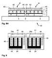
- FIG. 4illustrates, in a cross-sectional view, a multi-chip module 20 according to a second embodiment of the present invention.
- This multi-chip module 20also comprises two semiconductor chips 2 attached to the upper surface of a common substrate 3 in the face-down state via solder balls 4 .
- the backsides of the semiconductor chips 2are again each covered with an adhesion layer 5 .
- the multi-chip module 20further comprises two grids 21 of connected fins attached to each of the backsides of the semiconductor chips 2 for surface enlargement. These grids 21 , which comprise a thermally conducting material such as copper, are bonded to the adhesion layers 5 coating the backsides of the chips 2 via solder bonds 6 .
- FIG. 5depicts a plan view of a semiconductor chip 2 of the multi-chip module 20 of FIG. 4 with a grid 21 of connected fins.
- the grid 21comprises a plurality of recesses 23 exposing the backside surface of the semiconductor chip 2 .
- the multi-chip module 20further comprises a manifold layer 30 attached to the grids 21 of the semiconductor chips 2 via a sealing 36 .
- the manifold layer 30comprises an inlet 31 which can be connected to a liquid or water source (not shown) and an outlet 33 .
- the manifold layer 30further comprises an inlet channel 32 , an outlet channel 34 and a number of channels 35 extending from the inlet channel 32 and the outlet channel 34 towards the recesses 23 of the grids 21 .
- the inlet 31is connected thereby with the inlet channel 32 and the outlet 33 with the outlet channel 34 .
- the inlet 31 of the manifold layer 30is connected to a water or liquid source (not shown).
- a cooling liquid 24flows towards the recesses 23 of the grids 21 via the inlet 31 , the inlet channel 32 and respective ones of the channels 35 of the manifold layer 30 , which can be seen from FIGS. 4 , 5 and 6 .
- the cooling liquid 24then flows down into the recesses 23 of the grids 21 , is warmed up and flows up as warmed cooling liquid 24 a , as can be seen from FIG. 4 .
- the warmed cooling liquid 24 aflows through respective ones of the channels 35 , the outlet channel 34 and the outlet 33 of the manifold layer 30 , which can be seen from FIGS. 4 and 6 .
- the recesses 23 of the grids 21preferably have a width of about 50 ⁇ m and a depth of about between 100 to 500 ⁇ m.
- the backside surface of the semiconductor chipsis enlarged.
- the solder bonds 6 and the adhesion layers 5 of the multi-chip module 20have thicknesses of less or about 1 ⁇ m, so that the thermally conduction from the backsides of the semiconductor chips 2 to the grids 21 of connected fins is improved. As a consequence, a higher cooling performance of the liquid or water-cooled multi-chip module 20 is realized.
- the manifold layer 30can comprise a rigid material like e.g. glass ceramics. In order to reduce stress induction to the multi-chip module 20 due to different thermal expansions of the manifold layer 30 and the semiconductor chips 2 , it is preferred that the manifold layer 30 comprises the same material as the semiconductor chips 2 , i.e. silicon.
- the manifold layer 30comprises a thinning 37 between the semiconductor chips 2 and between the inlet and outlet channels 32 , 34 , as indicated in FIGS. 4 and 6 .
- These imperfectionsare additionally compensated by the flexible sealing 36 , which consists e.g. of polydimethylsiloxane (PDMS).
- the sealing 36may also comprise an adhesive.
- the manifold layer 30can also comprise a flexible material having a low Young's modulus like PDMS. Thus, geometrical imperfections between the chips 2 and different thermal expansions of the manifold layer 30 and the chips 2 can also be compensated.
- each of the grids 21is attached to the whole backside surface of a respective one of the semiconductor chips 2 , mechanical stress due to different thermal expansions of the grids 21 and the semiconductor chips 2 can occur.
- the backsides of the semiconductor chips 2 of the multi-chip module 20can alternatively be provided with an array of free-standing frames 22 , as indicated in the plan view of a semiconductor chip 2 in FIG. 7 .
- the frames 22which also comprise recesses 23 for receiving the cooling liquid 24 , form a structure similar to the grid 21 .
- the manifold layer 30can also be attached to the frames 22 via the sealing 36 .
- stress release gaps 25are provided which allow a reduction of mechanical stress induction caused by different thermal expansions of a semiconductor chip 2 and the frames 22 .
- the backsides of the semiconductor chips 2 of the multi-chip module 20can also be provided with an array of free-standing studs or fins (not shown), whereas the manifold layer 30 can be attached to the studs or fins via a sealing.
- the cooling performance achieved by liquid or water coolingis possibly better due to a spreading and mixing of cooling liquid between the studs or fins as well.
- the delivery rate of the liquid or water source connected to the inlet 32 of the manifold layer 30is possibly higher, however, due to an increased pressure drop between the studs or fins.
- a manifold layeris attached to the thermally conducting structure, i.e. a grid of connected fins or an array of frames, studs or fins, which is attached to the backsides of the semiconductor chips 2 .
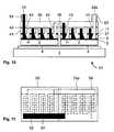
- FIGS. 8A to 8Hillustrate the fabrication process of a multi-chip module 40 according to a third embodiment of the present invention.
- a manifold structure or manifold layer 41 having an electro-conductive seed layer 11is provided, as shown in FIG. 8A .
- the manifold layer 41is covered with a top sealing 42 comprising holes 43 which serve as future inlet and outlet.
- a patterned mask layer 12e.g. photoresist having a recess structure is provided on the seed layer 11 .
- a thermally conducting materialsuch as copper is deposited on the patterned mask layer 12 to fill up the recess structure of the patterned mask layer 12 .
- This stepis e.g. performed by electroplating.
- a thermally conducting structure 21is formed by the thermally conducting material in the recess structure of the patterned mask layer 12 as can be seen in FIG. 8C .
- the thermally conducting structure 21exhibits the geometrical shape of the grid 21 of connected fins, for instance, which is depicted in the plan view of FIG. 5 .
- the thermally conducting structure 21could also comprise an array of frames, studs or fins.
- the patterned mask layer 12 and the thermally conducting structure 21are planarized by e.g. chemical and mechanical polishing to achieve a planar surface of the patterned mask layer 12 and the grid 21 .
- a solder 6is deposited on the grid 21 of connected fins, as illustrated in FIG. 8E . This step is for example carried out by electroplating.
- the patterned mask layer 12 and the seed layer 11 between the fins of the grid 21are removed by, for example, etching and the grid 21 of connected fins is transferred and solder-bonded to the backside of a semiconductor chip 2 .
- the backside of the semiconductor chip 2is again coated with an adhesion layer 5 .
- the adhesion layer 5can also be omitted.
- the front side of the semiconductor chip 2is provided with solder balls 4 , which can be performed by a standard C4 technology process.
- the semiconductor chip 2 depicted in FIG. 8G and a second chip 2 also fabricated in accordance with the process steps illustrated in FIGS. 8A to 8Gare mounted onto the upper surface of a common substrate 3 via soldering in order to obtain the multi-chip module 40 , which is depicted in FIG. 8H .
- FIGS. 8A to 8Hallows an enlargement of the backside surfaces of the semiconductor chips 2 with no or only little stress induction and without many changes in chip backend processing.
- the multi-chip module 40 or the semiconductor chips 2can also be re-worked if required by re-melting of the solder bonds 6 , removing a manifold layer 41 with a grid 21 and attaching another manifold layer 41 with a grid 21 to the backside of a semiconductor chip 2 .
- the fabrication process described with reference to FIGS. 8A to 8Hcan also be carried out with a bigger manifold layer, which extends over both of the semiconductor chips 2 when attached to the same (not shown).
- the multi-chip module 40 depicted in FIG. 8Hcomprises two separate manifold layers 31 .
- the manifold layers 41are connected to the grids 21 without a sealing.
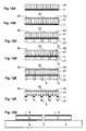
- FIG. 9shows a plan view of the manifold layers 41 of the multi-chip module 40 .
- Each of the manifold layers 41comprises an inlet channel 44 , an outlet channel 45 and channels 46 extending towards respective recesses 23 of the grids 21 .
- the inlet and outlet channels 44 , 45are connected to respective holes 43 of the top sealings 42 of the manifold layers 41 depicted in FIG. 8H , which serve as inlets and outlets.
- a flow of cooling liquid or water towards and away from the recesses 23 of the grids 21 of connected finscan be established.
- the manifold layers 41can again comprise a rigid or flexible material having a relatively low Young's modulus. In the case of a rigid material, it is preferred that the manifold layers 41 comprises the same material as the semiconductor chips 2 in order to reduce different thermal expansions of the manifold layers 41 and the semiconductor chips 2 .
- the multi-chip module 40can additionally be provided with a connection layer 50 attached to the manifold layers 41 , as illustrated in FIG. 10 .
- the connection layer 50comprises an inlet 51 and an outlet 53 .
- the inlet 51is connected to an inlet channel 52 and the outlet 53 is connected to an outlet channel 54 .
- the inlet channel 52 and the outlet channel 54can be seen from the plan view of the connection layer 50 depicted in FIG. 11 .
- the inlet and outlet channels 44 , 45 of the manifold layers 41are thereby connected to the inlet channel 52 and the outlet channel 54 of the connection layer 50 via respective ones of the holes 43 .
- a cooling liquid 24such as water flows towards the recesses 23 of the grids 21 via the inlet 51 and the inlet channel 52 of the connection layer 50 , the inlet channels 44 and respective ones of the channels 46 of the manifold layers 41 , and warmed cooling liquid 24 a flows away from the recesses 23 of the grids 21 towards the outlet 53 of the connection layer 50 via respective ones of the channels 46 , the outlet channels 45 and the outlet channel 54 , which can be seen from FIGS. 9 , 10 and 11 .
- connection layer 50can also comprise either a rigid or a flexible material having a relatively low Young's modulus.
- the connection layer 50preferably comprises the same material as the manifold layers 41 in order to reduce different thermal expansions.
- the connection layer 50can additionally be provided with a thinning 55 between the manifold layers 41 in order to compensate geometrical imperfections.
- FIGS. 12A to 12Gillustrate another fabrication process to provide the multi-chip module 40 as an alternative to the fabrication process described with reference to FIGS. 8A to 8H .
- This alternative fabrication processcomprises the same or similar process steps in order to provide a manifold layer 41 with a thermally conducting structure attached to the same, e.g. a grid 21 of connected fins, which is depicted in FIG. 12F .
- semiconductor chips 2are mounted onto the upper surface of a common substrate 3 separately from the manifold layers 41 , which can be seen from FIG. 12G .
- the semiconductor chips 2are again attached to the substrate 3 in a face-down state via solder balls 4 by utilizing e.g. a standard C4 technology process and comprise adhesion layers 5 coating the backsides.
- manifold layers 41 with grids 21are attached to the backsides of the semiconductor chips 2 via soldering in order to obtain the multi-chip module 40 depicted in FIG. 8H .
- a melting of the solder bonds 6 joined with an adhesion layer 5 due to mounting of a chip 2 onto the substrate 3 via soldering and a complete or partial dissolving of a grid 21 from the backside of the semiconductor chip 2 as a consequence thereof, which might occur during the previously described fabrication process illustrated in FIGS. 8A to 8His reduced.
- FIGS. 13 and 14Next, another aspect of the present invention will be described with reference to FIGS. 13 and 14 .
- FIG. 13depicts a schematic cross-sectional view of a part of a manifold layer 41 attached to a structural element of a thermally conducting structure, which is a stud 7 , for instance, via a spring element 47 and FIG. 14 depicts a plan view of the same.
- spring elements 47connecting the manifold layer 41 to the structural elements of a thermally conducting structure, the manifold layer 41 is mechanically decoupled from the thermally conducting structure.
- the spring elements 47can also be introduced between the manifold layers 41 and the grids 21 of the multi-chip module 40 of FIG. 8H and between the manifold layer 30 and the grids 21 of the multi-chip module 20 depicted in FIG. 4 , respectively.
- geometrical imperfections and different thermal expansions of e.g. a manifold layer and a thermally conducting structurecan be at least partially compensated so that mechanical stress induction to semiconductor chips and multi-chip modules, respectively, is further reduced. This allows the use of hybrid material systems with improved thermally capabilities such as solders for enhanced thermally transfer and reliability.
- a carriercomprising a manifold layer having a structured seed layer is provided in a first step.
- the structured seed layerprovides spring elements formed out of partitions of the seed layer.
- the seed layer 11 of the manifold layer 41 depicted in FIGS. 8A and 12Acan be partially formed in such a way as to provide spring elements.
- the subsequent processing stepsare carried out similar to the fabrication processes described above with reference to FIGS. 8A to 8H and FIGS. 12A to 12G , respectively, and in such a way that the structural elements of the thermally conducting structure, e.g. the fins of a grid 21 , are attached to these spring elements.
- thermally conducting structures depicted in the preceding figuresall have structural elements with essentially vertical side walls. Furthermore semiconductor devices comprising thermally conducting structures with different geometrical shapes are imaginable. Such thermally conducting structures can also be formed and attached to a semiconductor device by utilizing one of the fabrication methods described above.
- FIG. 15depicts, in a cross-sectional view, a semiconductor chip 2 with a thermally conducting structure comprising T-shaped fins 60 attached to the backside of the semiconductor chip 2 via solder bonds 6 .
- the T-shaped fins 60are essentially formed of a thermally conducting material like e.g. copper.
- the backside of the semiconductor chip 2is again coated with an adhesion layer 5 .
- the T-shaped fins 60build reentrant cavities acting as vapor traps, which are known to reduce the superheat by a factor of ten for two phase heat transfer systems.
- the semiconductor chip 2 shown in FIG. 15 or a multi-chip module comprising such semiconductor chips 2can be integrated into a device for two phase heat transfer, thus improving the thermally performance and the critical heat flux.
- fabrication methods described aboveare not limited to only semiconductor chips and multi-chip modules, respectively.
- the fabrication processescan also be carried out to transfer and attach thermally conducting structures formed on respective carriers to the backside surface of a semiconductor wafer, which is subsequently diced into semiconductor chips.
- the fabrication methods described abovemay also be used to manufacture other functional components on a carrier and to transfer and attach these components to the backside of a semiconductor device.
- Such functional componentscan e.g. comprise micro-electromechanical (MEMS) devices such as valves or pumps.
- MEMSmicro-electromechanical
- the fabrication methodscan be utilized to stack layers on the surface of a semiconductor device.
Landscapes
- Engineering & Computer Science (AREA)
- Physics & Mathematics (AREA)
- Condensed Matter Physics & Semiconductors (AREA)
- General Physics & Mathematics (AREA)
- Computer Hardware Design (AREA)
- Microelectronics & Electronic Packaging (AREA)
- Power Engineering (AREA)
- Manufacturing & Machinery (AREA)
- Chemical & Material Sciences (AREA)
- Materials Engineering (AREA)
- Cooling Or The Like Of Semiconductors Or Solid State Devices (AREA)
Abstract
Description
Claims (9)
Priority Applications (1)
| Application Number | Priority Date | Filing Date | Title |
|---|---|---|---|
| US12/709,674US7928565B2 (en) | 2004-06-15 | 2010-02-22 | Semiconductor device with a high thermal dissipation efficiency |
Applications Claiming Priority (4)
| Application Number | Priority Date | Filing Date | Title |
|---|---|---|---|
| EP04405362 | 2004-06-15 | ||
| EP04405362.7 | 2004-06-15 | ||
| US11/852,317US7713789B2 (en) | 2004-06-15 | 2007-09-09 | Semiconductor device with a high thermal dissipation efficiency |
| US12/709,674US7928565B2 (en) | 2004-06-15 | 2010-02-22 | Semiconductor device with a high thermal dissipation efficiency |
Related Parent Applications (1)
| Application Number | Title | Priority Date | Filing Date |
|---|---|---|---|
| US11/852,317DivisionUS7713789B2 (en) | 2004-06-15 | 2007-09-09 | Semiconductor device with a high thermal dissipation efficiency |
Publications (2)
| Publication Number | Publication Date |
|---|---|
| US20100148358A1 US20100148358A1 (en) | 2010-06-17 |
| US7928565B2true US7928565B2 (en) | 2011-04-19 |
Family
ID=35461086
Family Applications (3)
| Application Number | Title | Priority Date | Filing Date |
|---|---|---|---|
| US11/148,737Expired - LifetimeUS7271034B2 (en) | 2004-06-15 | 2005-06-09 | Semiconductor device with a high thermal dissipation efficiency |
| US11/852,317Expired - LifetimeUS7713789B2 (en) | 2004-06-15 | 2007-09-09 | Semiconductor device with a high thermal dissipation efficiency |
| US12/709,674ActiveUS7928565B2 (en) | 2004-06-15 | 2010-02-22 | Semiconductor device with a high thermal dissipation efficiency |
Family Applications Before (2)
| Application Number | Title | Priority Date | Filing Date |
|---|---|---|---|
| US11/148,737Expired - LifetimeUS7271034B2 (en) | 2004-06-15 | 2005-06-09 | Semiconductor device with a high thermal dissipation efficiency |
| US11/852,317Expired - LifetimeUS7713789B2 (en) | 2004-06-15 | 2007-09-09 | Semiconductor device with a high thermal dissipation efficiency |
Country Status (1)
| Country | Link |
|---|---|
| US (3) | US7271034B2 (en) |
Cited By (51)
| Publication number | Priority date | Publication date | Assignee | Title |
|---|---|---|---|---|
| US8408725B1 (en) | 2011-09-16 | 2013-04-02 | Lighting Science Group Corporation | Remote light wavelength conversion device and associated methods |
| US8465167B2 (en) | 2011-09-16 | 2013-06-18 | Lighting Science Group Corporation | Color conversion occlusion and associated methods |
| US8545034B2 (en) | 2012-01-24 | 2013-10-01 | Lighting Science Group Corporation | Dual characteristic color conversion enclosure and associated methods |
| US8608348B2 (en) | 2011-05-13 | 2013-12-17 | Lighting Science Group Corporation | Sealed electrical device with cooling system and associated methods |
| US8680457B2 (en) | 2012-05-07 | 2014-03-25 | Lighting Science Group Corporation | Motion detection system and associated methods having at least one LED of second set of LEDs to vary its voltage |
| US8686641B2 (en) | 2011-12-05 | 2014-04-01 | Biological Illumination, Llc | Tunable LED lamp for producing biologically-adjusted light |
| US8730558B2 (en) | 2011-03-28 | 2014-05-20 | Lighting Science Group Corporation | Wavelength converting lighting device and associated methods |
| US8743023B2 (en) | 2010-07-23 | 2014-06-03 | Biological Illumination, Llc | System for generating non-homogenous biologically-adjusted light and associated methods |
| US8754832B2 (en) | 2011-05-15 | 2014-06-17 | Lighting Science Group Corporation | Lighting system for accenting regions of a layer and associated methods |
| US8760370B2 (en) | 2011-05-15 | 2014-06-24 | Lighting Science Group Corporation | System for generating non-homogenous light and associated methods |
| US8761447B2 (en) | 2010-11-09 | 2014-06-24 | Biological Illumination, Llc | Sustainable outdoor lighting system for use in environmentally photo-sensitive area |
| US8841864B2 (en) | 2011-12-05 | 2014-09-23 | Biological Illumination, Llc | Tunable LED lamp for producing biologically-adjusted light |
| US8866414B2 (en) | 2011-12-05 | 2014-10-21 | Biological Illumination, Llc | Tunable LED lamp for producing biologically-adjusted light |
| US8899776B2 (en) | 2012-05-07 | 2014-12-02 | Lighting Science Group Corporation | Low-angle thoroughfare surface lighting device |
| US8901850B2 (en) | 2012-05-06 | 2014-12-02 | Lighting Science Group Corporation | Adaptive anti-glare light system and associated methods |
| US8899775B2 (en) | 2013-03-15 | 2014-12-02 | Lighting Science Group Corporation | Low-angle thoroughfare surface lighting device |
| US8963450B2 (en) | 2011-12-05 | 2015-02-24 | Biological Illumination, Llc | Adaptable biologically-adjusted indirect lighting device and associated methods |
| USD723729S1 (en) | 2013-03-15 | 2015-03-03 | Lighting Science Group Corporation | Low bay luminaire |
| US9006987B2 (en) | 2012-05-07 | 2015-04-14 | Lighting Science Group, Inc. | Wall-mountable luminaire and associated systems and methods |
| US9024536B2 (en) | 2011-12-05 | 2015-05-05 | Biological Illumination, Llc | Tunable LED lamp for producing biologically-adjusted light and associated methods |
| US9127818B2 (en) | 2012-10-03 | 2015-09-08 | Lighting Science Group Corporation | Elongated LED luminaire and associated methods |
| US9151482B2 (en) | 2011-05-13 | 2015-10-06 | Lighting Science Group Corporation | Sealed electrical device with cooling system |
| US9157581B2 (en) | 2009-10-05 | 2015-10-13 | Lighting Science Group Corporation | Low profile luminaire with light guide and associated systems and methods |
| US9173269B2 (en) | 2011-05-15 | 2015-10-27 | Lighting Science Group Corporation | Lighting system for accentuating regions of a layer and associated methods |
| US9174067B2 (en) | 2012-10-15 | 2015-11-03 | Biological Illumination, Llc | System for treating light treatable conditions and associated methods |
| US9185783B2 (en) | 2011-05-15 | 2015-11-10 | Lighting Science Group Corporation | Wireless pairing system and associated methods |
| US9220202B2 (en) | 2011-12-05 | 2015-12-29 | Biological Illumination, Llc | Lighting system to control the circadian rhythm of agricultural products and associated methods |
| US9255670B2 (en) | 2013-03-15 | 2016-02-09 | Lighting Science Group Corporation | Street lighting device for communicating with observers and associated methods |
| US9289574B2 (en) | 2011-12-05 | 2016-03-22 | Biological Illumination, Llc | Three-channel tuned LED lamp for producing biologically-adjusted light |
| US9303825B2 (en) | 2013-03-05 | 2016-04-05 | Lighting Science Group, Corporation | High bay luminaire |
| US9322516B2 (en) | 2012-11-07 | 2016-04-26 | Lighting Science Group Corporation | Luminaire having vented optical chamber and associated methods |
| US9347655B2 (en) | 2013-03-11 | 2016-05-24 | Lighting Science Group Corporation | Rotatable lighting device |
| US9360202B2 (en) | 2011-05-13 | 2016-06-07 | Lighting Science Group Corporation | System for actively cooling an LED filament and associated methods |
| US9402294B2 (en) | 2012-05-08 | 2016-07-26 | Lighting Science Group Corporation | Self-calibrating multi-directional security luminaire and associated methods |
| US9420240B2 (en) | 2011-05-15 | 2016-08-16 | Lighting Science Group Corporation | Intelligent security light and associated methods |
| US9429294B2 (en) | 2013-11-11 | 2016-08-30 | Lighting Science Group Corporation | System for directional control of light and associated methods |
| US9459397B2 (en) | 2013-03-12 | 2016-10-04 | Lighting Science Group Corporation | Edge lit lighting device |
| US9532423B2 (en) | 2010-07-23 | 2016-12-27 | Lighting Science Group Corporation | System and methods for operating a lighting device |
| US9581756B2 (en) | 2009-10-05 | 2017-02-28 | Lighting Science Group Corporation | Light guide for low profile luminaire |
| US9648284B2 (en) | 2011-05-15 | 2017-05-09 | Lighting Science Group Corporation | Occupancy sensor and associated methods |
| US9681522B2 (en) | 2012-05-06 | 2017-06-13 | Lighting Science Group Corporation | Adaptive light system and associated methods |
| US9693414B2 (en) | 2011-12-05 | 2017-06-27 | Biological Illumination, Llc | LED lamp for producing biologically-adjusted light |
| US9748381B1 (en) | 2016-10-11 | 2017-08-29 | International Business Machines Corporation | Pillar formation for heat dissipation and isolation in vertical field effect transistors |
| US9827439B2 (en) | 2010-07-23 | 2017-11-28 | Biological Illumination, Llc | System for dynamically adjusting circadian rhythm responsive to scheduled events and associated methods |
| US9953899B2 (en) | 2015-09-30 | 2018-04-24 | Microfabrica Inc. | Micro heat transfer arrays, micro cold plates, and thermal management systems for cooling semiconductor devices, and methods for using and making such arrays, plates, and systems |
| US10096537B1 (en) | 2015-12-31 | 2018-10-09 | Microfabrica Inc. | Thermal management systems, methods for making, and methods for using |
| US10490482B1 (en)* | 2018-12-05 | 2019-11-26 | Toyota Motor Engineering & Manufacturing North America, Inc. | Cooling devices including jet cooling with an intermediate mesh and methods for using the same |
| US10743442B2 (en) | 2018-12-11 | 2020-08-11 | Toyota Motor Engineering & Manufacturing North America, Inc. | Cooling devices including jet cooling with an intermediate mesh and methods for using the same |
| US11121061B2 (en) | 2018-11-20 | 2021-09-14 | Toyota Motor Engineering & Manufacturing North America, Inc. | Cooling chip structures having a jet impingement system and assembly having the same |
| US12255123B2 (en) | 2015-09-30 | 2025-03-18 | Microfabrica Inc. | Micro heat transfer arrays, micro cold plates, and thermal management systems for semiconductor devices, and methods for using and making such arrays, plates, and systems |
| US12414266B2 (en) | 2020-10-31 | 2025-09-09 | Huawei Technologies Co., Ltd. | Cooling apparatus and electronic device |
Families Citing this family (23)
| Publication number | Priority date | Publication date | Assignee | Title |
|---|---|---|---|---|
| US7271034B2 (en)* | 2004-06-15 | 2007-09-18 | International Business Machines Corporation | Semiconductor device with a high thermal dissipation efficiency |
| US8541876B2 (en) | 2005-09-30 | 2013-09-24 | Intel Corporation | Microelectronic package having direct contact heat spreader and method of manufacturing same |
| US7456479B2 (en)* | 2005-12-15 | 2008-11-25 | United Microelectronics Corp. | Method for fabricating a probing pad of an integrated circuit chip |
| US7769455B2 (en) | 2006-01-27 | 2010-08-03 | Cyberonics, Inc. | Power supply monitoring for an implantable device |
| US8456023B2 (en)* | 2007-04-27 | 2013-06-04 | Freescale Semiconductor, Inc. | Semiconductor wafer processing |
| US20090084931A1 (en)* | 2007-09-27 | 2009-04-02 | Intel Corporation | Enabling bare die liquid cooling for the bare die and hot spots |
| US8283776B2 (en) | 2010-01-26 | 2012-10-09 | Qualcomm Incorporated | Microfabricated pillar fins for thermal management |
| TWI446495B (en)* | 2011-01-19 | 2014-07-21 | Subtron Technology Co Ltd | Package carrier board and manufacturing method thereof |
| US9184108B2 (en)* | 2011-12-08 | 2015-11-10 | Oracle International Corporation | Heat dissipation structure for an integrated circuit (IC) chip |
| US9391000B2 (en)* | 2012-04-11 | 2016-07-12 | Taiwan Semiconductor Manufacturing Company, Ltd. | Methods for forming silicon-based hermetic thermal solutions |
| US9735087B2 (en) | 2012-09-20 | 2017-08-15 | Taiwan Semiconductor Manufacturing Company, Ltd. | Wafer level embedded heat spreader |
| US9230878B2 (en)* | 2013-04-12 | 2016-01-05 | Lenovo Enterprise Solutions (Singapore) Pte. Ltd. | Integrated circuit package for heat dissipation |
| US8987892B2 (en)* | 2013-05-10 | 2015-03-24 | Raytheon Company | Method for creating a selective solder seal interface for an integrated circuit cooling system |
| KR101695708B1 (en)* | 2014-01-09 | 2017-01-13 | 한국전자통신연구원 | Semiconductor device and method of fabricating the same |
| US9263366B2 (en)* | 2014-05-30 | 2016-02-16 | International Business Machines Corporation | Liquid cooling of semiconductor chips utilizing small scale structures |
| EP3498061B1 (en)* | 2016-08-11 | 2021-06-16 | Sharfi, Benjamin K. | Isolating liquid cool shock protection |
| WO2019005107A1 (en)* | 2017-06-30 | 2019-01-03 | Intel Corporation | Die backside structures for enhancing liquid cooling of high power multi-chip package (mcp) dice |
| KR102566772B1 (en)* | 2018-11-09 | 2023-08-14 | 삼성전자주식회사 | Semiconductor package |
| US11081424B2 (en)* | 2019-06-18 | 2021-08-03 | International Business Machines Corporation | Micro-fluidic channels having various critical dimensions |
| US11328975B2 (en)* | 2019-11-26 | 2022-05-10 | Taiwan Semiconductor Manufacturing Company, Ltd. | Semiconductor device |
| US11830786B2 (en)* | 2020-12-28 | 2023-11-28 | Innoscience (Suzhou) Technology Co., Ltd. | Semiconductor package and method for manufacturing the same |
| EP4340010B1 (en)* | 2021-07-14 | 2025-06-25 | Huawei Technologies Co., Ltd. | Chip packaging structure and packaging method and electronic device |
| CN117855171B (en)* | 2024-03-07 | 2024-05-03 | 江苏中科智芯集成科技有限公司 | Micro-channel heat dissipation structure of high-power chip and processing technology thereof |
Citations (2)
| Publication number | Priority date | Publication date | Assignee | Title |
|---|---|---|---|---|
| US20030017634A1 (en)* | 1997-05-22 | 2003-01-23 | Semiconductor Energy Laboratory Co., Ltd. | Electro-optical device |
| US6903929B2 (en)* | 2003-03-31 | 2005-06-07 | Intel Corporation | Two-phase cooling utilizing microchannel heat exchangers and channeled heat sink |
Family Cites Families (11)
| Publication number | Priority date | Publication date | Assignee | Title |
|---|---|---|---|---|
| US5842275A (en)* | 1995-09-05 | 1998-12-01 | Ford Motor Company | Reflow soldering to mounting pads with vent channels to avoid skewing |
| JP3518434B2 (en)* | 1999-08-11 | 2004-04-12 | 株式会社日立製作所 | Multi-chip module cooling system |
| US6908784B1 (en)* | 2002-03-06 | 2005-06-21 | Micron Technology, Inc. | Method for fabricating encapsulated semiconductor components |
| US6639800B1 (en)* | 2002-04-30 | 2003-10-28 | Advanced Micro Devices, Inc. | Heat sink subassembly |
| JP3934565B2 (en)* | 2003-02-21 | 2007-06-20 | 富士通株式会社 | Semiconductor device |
| US6934154B2 (en)* | 2003-03-31 | 2005-08-23 | Intel Corporation | Micro-channel heat exchangers and spreaders |
| JP3994924B2 (en)* | 2003-06-02 | 2007-10-24 | セイコーエプソン株式会社 | Circuit board manufacturing method |
| US7091586B2 (en)* | 2003-11-04 | 2006-08-15 | Intel Corporation | Detachable on package voltage regulation module |
| US7115987B2 (en)* | 2003-12-31 | 2006-10-03 | Intel Corporation | Integrated stacked microchannel heat exchanger and heat spreader |
| US6919231B1 (en)* | 2004-03-24 | 2005-07-19 | Intel Corporation | Methods of forming channels on an integrated circuit die and die cooling systems including such channels |
| US7271034B2 (en)* | 2004-06-15 | 2007-09-18 | International Business Machines Corporation | Semiconductor device with a high thermal dissipation efficiency |
- 2005
- 2005-06-09USUS11/148,737patent/US7271034B2/ennot_activeExpired - Lifetime
- 2007
- 2007-09-09USUS11/852,317patent/US7713789B2/ennot_activeExpired - Lifetime
- 2010
- 2010-02-22USUS12/709,674patent/US7928565B2/enactiveActive
Patent Citations (2)
| Publication number | Priority date | Publication date | Assignee | Title |
|---|---|---|---|---|
| US20030017634A1 (en)* | 1997-05-22 | 2003-01-23 | Semiconductor Energy Laboratory Co., Ltd. | Electro-optical device |
| US6903929B2 (en)* | 2003-03-31 | 2005-06-07 | Intel Corporation | Two-phase cooling utilizing microchannel heat exchangers and channeled heat sink |
Cited By (67)
| Publication number | Priority date | Publication date | Assignee | Title |
|---|---|---|---|---|
| US9157581B2 (en) | 2009-10-05 | 2015-10-13 | Lighting Science Group Corporation | Low profile luminaire with light guide and associated systems and methods |
| US9435930B2 (en) | 2009-10-05 | 2016-09-06 | Lighting Science Group Corporation | Low profile luminaire and associated systems and methods |
| US9581756B2 (en) | 2009-10-05 | 2017-02-28 | Lighting Science Group Corporation | Light guide for low profile luminaire |
| US9827439B2 (en) | 2010-07-23 | 2017-11-28 | Biological Illumination, Llc | System for dynamically adjusting circadian rhythm responsive to scheduled events and associated methods |
| US9265968B2 (en) | 2010-07-23 | 2016-02-23 | Biological Illumination, Llc | System for generating non-homogenous biologically-adjusted light and associated methods |
| US9532423B2 (en) | 2010-07-23 | 2016-12-27 | Lighting Science Group Corporation | System and methods for operating a lighting device |
| US8743023B2 (en) | 2010-07-23 | 2014-06-03 | Biological Illumination, Llc | System for generating non-homogenous biologically-adjusted light and associated methods |
| US8761447B2 (en) | 2010-11-09 | 2014-06-24 | Biological Illumination, Llc | Sustainable outdoor lighting system for use in environmentally photo-sensitive area |
| US9036868B2 (en) | 2010-11-09 | 2015-05-19 | Biological Illumination, Llc | Sustainable outdoor lighting system for use in environmentally photo-sensitive area |
| US9036244B2 (en) | 2011-03-28 | 2015-05-19 | Lighting Science Group Corporation | Wavelength converting lighting device and associated methods |
| US8730558B2 (en) | 2011-03-28 | 2014-05-20 | Lighting Science Group Corporation | Wavelength converting lighting device and associated methods |
| US9360202B2 (en) | 2011-05-13 | 2016-06-07 | Lighting Science Group Corporation | System for actively cooling an LED filament and associated methods |
| US9151482B2 (en) | 2011-05-13 | 2015-10-06 | Lighting Science Group Corporation | Sealed electrical device with cooling system |
| US8608348B2 (en) | 2011-05-13 | 2013-12-17 | Lighting Science Group Corporation | Sealed electrical device with cooling system and associated methods |
| US9185783B2 (en) | 2011-05-15 | 2015-11-10 | Lighting Science Group Corporation | Wireless pairing system and associated methods |
| US9648284B2 (en) | 2011-05-15 | 2017-05-09 | Lighting Science Group Corporation | Occupancy sensor and associated methods |
| US9420240B2 (en) | 2011-05-15 | 2016-08-16 | Lighting Science Group Corporation | Intelligent security light and associated methods |
| US8754832B2 (en) | 2011-05-15 | 2014-06-17 | Lighting Science Group Corporation | Lighting system for accenting regions of a layer and associated methods |
| US9681108B2 (en) | 2011-05-15 | 2017-06-13 | Lighting Science Group Corporation | Occupancy sensor and associated methods |
| US8760370B2 (en) | 2011-05-15 | 2014-06-24 | Lighting Science Group Corporation | System for generating non-homogenous light and associated methods |
| US9173269B2 (en) | 2011-05-15 | 2015-10-27 | Lighting Science Group Corporation | Lighting system for accentuating regions of a layer and associated methods |
| US9595118B2 (en) | 2011-05-15 | 2017-03-14 | Lighting Science Group Corporation | System for generating non-homogenous light and associated methods |
| US8702259B2 (en) | 2011-09-16 | 2014-04-22 | Lighting Science Group Corporation | Color conversion occlusion and associated methods |
| US8408725B1 (en) | 2011-09-16 | 2013-04-02 | Lighting Science Group Corporation | Remote light wavelength conversion device and associated methods |
| US8616715B2 (en) | 2011-09-16 | 2013-12-31 | Lighting Science Group Corporation | Remote light wavelength conversion device and associated methods |
| US8465167B2 (en) | 2011-09-16 | 2013-06-18 | Lighting Science Group Corporation | Color conversion occlusion and associated methods |
| US9220202B2 (en) | 2011-12-05 | 2015-12-29 | Biological Illumination, Llc | Lighting system to control the circadian rhythm of agricultural products and associated methods |
| US9131573B2 (en) | 2011-12-05 | 2015-09-08 | Biological Illumination, Llc | Tunable LED lamp for producing biologically-adjusted light |
| US8841864B2 (en) | 2011-12-05 | 2014-09-23 | Biological Illumination, Llc | Tunable LED lamp for producing biologically-adjusted light |
| US9024536B2 (en) | 2011-12-05 | 2015-05-05 | Biological Illumination, Llc | Tunable LED lamp for producing biologically-adjusted light and associated methods |
| US8686641B2 (en) | 2011-12-05 | 2014-04-01 | Biological Illumination, Llc | Tunable LED lamp for producing biologically-adjusted light |
| US8941329B2 (en) | 2011-12-05 | 2015-01-27 | Biological Illumination, Llc | Tunable LED lamp for producing biologically-adjusted light |
| US9913341B2 (en) | 2011-12-05 | 2018-03-06 | Biological Illumination, Llc | LED lamp for producing biologically-adjusted light including a cyan LED |
| US8866414B2 (en) | 2011-12-05 | 2014-10-21 | Biological Illumination, Llc | Tunable LED lamp for producing biologically-adjusted light |
| US8963450B2 (en) | 2011-12-05 | 2015-02-24 | Biological Illumination, Llc | Adaptable biologically-adjusted indirect lighting device and associated methods |
| US9289574B2 (en) | 2011-12-05 | 2016-03-22 | Biological Illumination, Llc | Three-channel tuned LED lamp for producing biologically-adjusted light |
| US9693414B2 (en) | 2011-12-05 | 2017-06-27 | Biological Illumination, Llc | LED lamp for producing biologically-adjusted light |
| US8545034B2 (en) | 2012-01-24 | 2013-10-01 | Lighting Science Group Corporation | Dual characteristic color conversion enclosure and associated methods |
| US9681522B2 (en) | 2012-05-06 | 2017-06-13 | Lighting Science Group Corporation | Adaptive light system and associated methods |
| US8901850B2 (en) | 2012-05-06 | 2014-12-02 | Lighting Science Group Corporation | Adaptive anti-glare light system and associated methods |
| US8680457B2 (en) | 2012-05-07 | 2014-03-25 | Lighting Science Group Corporation | Motion detection system and associated methods having at least one LED of second set of LEDs to vary its voltage |
| US9006987B2 (en) | 2012-05-07 | 2015-04-14 | Lighting Science Group, Inc. | Wall-mountable luminaire and associated systems and methods |
| US8899776B2 (en) | 2012-05-07 | 2014-12-02 | Lighting Science Group Corporation | Low-angle thoroughfare surface lighting device |
| US9402294B2 (en) | 2012-05-08 | 2016-07-26 | Lighting Science Group Corporation | Self-calibrating multi-directional security luminaire and associated methods |
| US9353916B2 (en) | 2012-10-03 | 2016-05-31 | Lighting Science Group Corporation | Elongated LED luminaire and associated methods |
| US9127818B2 (en) | 2012-10-03 | 2015-09-08 | Lighting Science Group Corporation | Elongated LED luminaire and associated methods |
| US9174067B2 (en) | 2012-10-15 | 2015-11-03 | Biological Illumination, Llc | System for treating light treatable conditions and associated methods |
| US9322516B2 (en) | 2012-11-07 | 2016-04-26 | Lighting Science Group Corporation | Luminaire having vented optical chamber and associated methods |
| US9303825B2 (en) | 2013-03-05 | 2016-04-05 | Lighting Science Group, Corporation | High bay luminaire |
| US9347655B2 (en) | 2013-03-11 | 2016-05-24 | Lighting Science Group Corporation | Rotatable lighting device |
| US9459397B2 (en) | 2013-03-12 | 2016-10-04 | Lighting Science Group Corporation | Edge lit lighting device |
| USD723729S1 (en) | 2013-03-15 | 2015-03-03 | Lighting Science Group Corporation | Low bay luminaire |
| US9255670B2 (en) | 2013-03-15 | 2016-02-09 | Lighting Science Group Corporation | Street lighting device for communicating with observers and associated methods |
| US9631780B2 (en) | 2013-03-15 | 2017-04-25 | Lighting Science Group Corporation | Street lighting device for communicating with observers and associated methods |
| US8899775B2 (en) | 2013-03-15 | 2014-12-02 | Lighting Science Group Corporation | Low-angle thoroughfare surface lighting device |
| US9429294B2 (en) | 2013-11-11 | 2016-08-30 | Lighting Science Group Corporation | System for directional control of light and associated methods |
| US10957624B2 (en) | 2015-09-30 | 2021-03-23 | Microfabrica Inc. | Micro heat transfer arrays, micro cold plates, and thermal management systems for cooling semiconductor devices, and methods for using and making such arrays, plates, and systems |
| US12255123B2 (en) | 2015-09-30 | 2025-03-18 | Microfabrica Inc. | Micro heat transfer arrays, micro cold plates, and thermal management systems for semiconductor devices, and methods for using and making such arrays, plates, and systems |
| US9953899B2 (en) | 2015-09-30 | 2018-04-24 | Microfabrica Inc. | Micro heat transfer arrays, micro cold plates, and thermal management systems for cooling semiconductor devices, and methods for using and making such arrays, plates, and systems |
| US11456235B1 (en) | 2015-09-30 | 2022-09-27 | Microfabrica Inc. | Micro heat transfer arrays, micro cold plates, and thermal management systems for cooling semiconductor devices, and methods for using and making such arrays, plates, and systems |
| US10665530B2 (en) | 2015-09-30 | 2020-05-26 | Microfabrica Inc. | Micro heat transfer arrays, micro cold plates, and thermal management systems for cooling semiconductor devices, and methods for using and making such arrays, plates, and systems |
| US10096537B1 (en) | 2015-12-31 | 2018-10-09 | Microfabrica Inc. | Thermal management systems, methods for making, and methods for using |
| US9748381B1 (en) | 2016-10-11 | 2017-08-29 | International Business Machines Corporation | Pillar formation for heat dissipation and isolation in vertical field effect transistors |
| US11121061B2 (en) | 2018-11-20 | 2021-09-14 | Toyota Motor Engineering & Manufacturing North America, Inc. | Cooling chip structures having a jet impingement system and assembly having the same |
| US10490482B1 (en)* | 2018-12-05 | 2019-11-26 | Toyota Motor Engineering & Manufacturing North America, Inc. | Cooling devices including jet cooling with an intermediate mesh and methods for using the same |
| US10743442B2 (en) | 2018-12-11 | 2020-08-11 | Toyota Motor Engineering & Manufacturing North America, Inc. | Cooling devices including jet cooling with an intermediate mesh and methods for using the same |
| US12414266B2 (en) | 2020-10-31 | 2025-09-09 | Huawei Technologies Co., Ltd. | Cooling apparatus and electronic device |
Also Published As
| Publication number | Publication date |
|---|---|
| US20100148358A1 (en) | 2010-06-17 |
| US7271034B2 (en) | 2007-09-18 |
| US7713789B2 (en) | 2010-05-11 |
| US20080017978A1 (en) | 2008-01-24 |
| US20050277280A1 (en) | 2005-12-15 |
Similar Documents
| Publication | Publication Date | Title |
|---|---|---|
| US7928565B2 (en) | Semiconductor device with a high thermal dissipation efficiency | |
| CN113257757B (en) | A kind of silicon-based fan-out package structure and preparation method thereof | |
| US11458717B2 (en) | Four D device process and structure | |
| US20240203823A1 (en) | Integrated systems for cooling high powered devices and methods of manufacturing the same | |
| US7888786B2 (en) | Electronic module comprising memory and integrated circuit processor chips formed on a microchannel cooling device | |
| JP5114414B2 (en) | Integrated microchannel for 3D through silicon architecture | |
| US7049697B2 (en) | Process for making fine pitch connections between devices and structure made by the process | |
| CN114300428B (en) | A microchannel packaging structure capable of dissipating heat on six sides and a manufacturing method thereof | |
| US20240128150A1 (en) | Semiconductor package structure for enhanced cooling | |
| CN114446907A (en) | Active heat dissipation packaging method and structure for three-dimensional integrated TSV pin fin micro channel | |
| CN113241332B (en) | Semiconductor structure with micro-channel, chip stacking structure and preparation method | |
| CN116130436B (en) | Packaging structure integrated with porous micro-channel heat dissipation structure array and preparation method thereof | |
| CN221102070U (en) | Package | |
| CN114429938A (en) | A three-dimensional integrated embedded micro-channel active heat dissipation packaging method and structure | |
| TW202516697A (en) | Integrated cooling assemblies including backside power/ground delivery and methods of manufacturing the same | |
| Steller et al. | Microfluidic Interposer for High Performance Fluidic Chip Cooling | |
| CN112908860B (en) | High bandwidth memory structure and method for making same | |
| CN119650532B (en) | A microchannel packaging structure based on coolant cooling and packaging method thereof | |
| CN116613122A (en) | Heat sink compatible with micro-channel embedded in liquid silicon through hole communication hole and manufacturing method thereof | |
| CN115966476A (en) | Wafer-level chip packaging method and packaging structure | |
| CN114975317A (en) | Active heat dissipation packaging structure of embedded flat heat pipe and packaging method thereof |
Legal Events
| Date | Code | Title | Description |
|---|---|---|---|
| STCF | Information on status: patent grant | Free format text:PATENTED CASE | |
| FPAY | Fee payment | Year of fee payment:4 | |
| AS | Assignment | Owner name:GLOBALFOUNDRIES U.S. 2 LLC, NEW YORK Free format text:ASSIGNMENT OF ASSIGNORS INTEREST;ASSIGNOR:INTERNATIONAL BUSINESS MACHINES CORPORATION;REEL/FRAME:036550/0001 Effective date:20150629 | |
| AS | Assignment | Owner name:GLOBALFOUNDRIES INC., CAYMAN ISLANDS Free format text:ASSIGNMENT OF ASSIGNORS INTEREST;ASSIGNORS:GLOBALFOUNDRIES U.S. 2 LLC;GLOBALFOUNDRIES U.S. INC.;REEL/FRAME:036779/0001 Effective date:20150910 | |
| MAFP | Maintenance fee payment | Free format text:PAYMENT OF MAINTENANCE FEE, 8TH YEAR, LARGE ENTITY (ORIGINAL EVENT CODE: M1552); ENTITY STATUS OF PATENT OWNER: LARGE ENTITY Year of fee payment:8 | |
| AS | Assignment | Owner name:WILMINGTON TRUST, NATIONAL ASSOCIATION, DELAWARE Free format text:SECURITY AGREEMENT;ASSIGNOR:GLOBALFOUNDRIES INC.;REEL/FRAME:049490/0001 Effective date:20181127 | |
| AS | Assignment | Owner name:GLOBALFOUNDRIES U.S. INC., CALIFORNIA Free format text:ASSIGNMENT OF ASSIGNORS INTEREST;ASSIGNOR:GLOBALFOUNDRIES INC.;REEL/FRAME:054633/0001 Effective date:20201022 | |
| AS | Assignment | Owner name:GLOBALFOUNDRIES INC., CAYMAN ISLANDS Free format text:RELEASE BY SECURED PARTY;ASSIGNOR:WILMINGTON TRUST, NATIONAL ASSOCIATION;REEL/FRAME:054636/0001 Effective date:20201117 | |
| AS | Assignment | Owner name:GLOBALFOUNDRIES U.S. INC., NEW YORK Free format text:RELEASE BY SECURED PARTY;ASSIGNOR:WILMINGTON TRUST, NATIONAL ASSOCIATION;REEL/FRAME:056987/0001 Effective date:20201117 | |
| MAFP | Maintenance fee payment | Free format text:PAYMENT OF MAINTENANCE FEE, 12TH YEAR, LARGE ENTITY (ORIGINAL EVENT CODE: M1553); ENTITY STATUS OF PATENT OWNER: LARGE ENTITY Year of fee payment:12 |