US7928542B2 - Lead frame for semiconductor package - Google Patents
Lead frame for semiconductor packageDownload PDFInfo
- Publication number
- US7928542B2 US7928542B2US12/399,600US39960009AUS7928542B2US 7928542 B2US7928542 B2US 7928542B2US 39960009 AUS39960009 AUS 39960009AUS 7928542 B2US7928542 B2US 7928542B2
- Authority
- US
- United States
- Prior art keywords
- ground ring
- die pad
- leads
- semiconductor package
- opposed relation
- Prior art date
- Legal status (The legal status is an assumption and is not a legal conclusion. Google has not performed a legal analysis and makes no representation as to the accuracy of the status listed.)
- Expired - Fee Related, expires
Links
Images


Classifications
- H—ELECTRICITY
- H01—ELECTRIC ELEMENTS
- H01L—SEMICONDUCTOR DEVICES NOT COVERED BY CLASS H10
- H01L23/00—Details of semiconductor or other solid state devices
- H01L23/28—Encapsulations, e.g. encapsulating layers, coatings, e.g. for protection
- H01L23/31—Encapsulations, e.g. encapsulating layers, coatings, e.g. for protection characterised by the arrangement or shape
- H01L23/3107—Encapsulations, e.g. encapsulating layers, coatings, e.g. for protection characterised by the arrangement or shape the device being completely enclosed
- H—ELECTRICITY
- H01—ELECTRIC ELEMENTS
- H01L—SEMICONDUCTOR DEVICES NOT COVERED BY CLASS H10
- H01L23/00—Details of semiconductor or other solid state devices
- H01L23/48—Arrangements for conducting electric current to or from the solid state body in operation, e.g. leads, terminal arrangements ; Selection of materials therefor
- H01L23/488—Arrangements for conducting electric current to or from the solid state body in operation, e.g. leads, terminal arrangements ; Selection of materials therefor consisting of soldered or bonded constructions
- H01L23/495—Lead-frames or other flat leads
- H01L23/49503—Lead-frames or other flat leads characterised by the die pad
- H—ELECTRICITY
- H01—ELECTRIC ELEMENTS
- H01L—SEMICONDUCTOR DEVICES NOT COVERED BY CLASS H10
- H01L23/00—Details of semiconductor or other solid state devices
- H01L23/48—Arrangements for conducting electric current to or from the solid state body in operation, e.g. leads, terminal arrangements ; Selection of materials therefor
- H01L23/488—Arrangements for conducting electric current to or from the solid state body in operation, e.g. leads, terminal arrangements ; Selection of materials therefor consisting of soldered or bonded constructions
- H01L23/495—Lead-frames or other flat leads
- H01L23/49541—Geometry of the lead-frame
- H01L23/49548—Cross section geometry
- H—ELECTRICITY
- H01—ELECTRIC ELEMENTS
- H01L—SEMICONDUCTOR DEVICES NOT COVERED BY CLASS H10
- H01L2224/00—Indexing scheme for arrangements for connecting or disconnecting semiconductor or solid-state bodies and methods related thereto as covered by H01L24/00
- H01L2224/01—Means for bonding being attached to, or being formed on, the surface to be connected, e.g. chip-to-package, die-attach, "first-level" interconnects; Manufacturing methods related thereto
- H01L2224/02—Bonding areas; Manufacturing methods related thereto
- H01L2224/04—Structure, shape, material or disposition of the bonding areas prior to the connecting process
- H01L2224/05—Structure, shape, material or disposition of the bonding areas prior to the connecting process of an individual bonding area
- H01L2224/0554—External layer
- H01L2224/05599—Material
- H—ELECTRICITY
- H01—ELECTRIC ELEMENTS
- H01L—SEMICONDUCTOR DEVICES NOT COVERED BY CLASS H10
- H01L2224/00—Indexing scheme for arrangements for connecting or disconnecting semiconductor or solid-state bodies and methods related thereto as covered by H01L24/00
- H01L2224/01—Means for bonding being attached to, or being formed on, the surface to be connected, e.g. chip-to-package, die-attach, "first-level" interconnects; Manufacturing methods related thereto
- H01L2224/26—Layer connectors, e.g. plate connectors, solder or adhesive layers; Manufacturing methods related thereto
- H01L2224/31—Structure, shape, material or disposition of the layer connectors after the connecting process
- H01L2224/32—Structure, shape, material or disposition of the layer connectors after the connecting process of an individual layer connector
- H01L2224/321—Disposition
- H01L2224/32151—Disposition the layer connector connecting between a semiconductor or solid-state body and an item not being a semiconductor or solid-state body, e.g. chip-to-substrate, chip-to-passive
- H01L2224/32221—Disposition the layer connector connecting between a semiconductor or solid-state body and an item not being a semiconductor or solid-state body, e.g. chip-to-substrate, chip-to-passive the body and the item being stacked
- H01L2224/32245—Disposition the layer connector connecting between a semiconductor or solid-state body and an item not being a semiconductor or solid-state body, e.g. chip-to-substrate, chip-to-passive the body and the item being stacked the item being metallic
- H—ELECTRICITY
- H01—ELECTRIC ELEMENTS
- H01L—SEMICONDUCTOR DEVICES NOT COVERED BY CLASS H10
- H01L2224/00—Indexing scheme for arrangements for connecting or disconnecting semiconductor or solid-state bodies and methods related thereto as covered by H01L24/00
- H01L2224/01—Means for bonding being attached to, or being formed on, the surface to be connected, e.g. chip-to-package, die-attach, "first-level" interconnects; Manufacturing methods related thereto
- H01L2224/42—Wire connectors; Manufacturing methods related thereto
- H01L2224/44—Structure, shape, material or disposition of the wire connectors prior to the connecting process
- H01L2224/45—Structure, shape, material or disposition of the wire connectors prior to the connecting process of an individual wire connector
- H01L2224/45001—Core members of the connector
- H01L2224/45099—Material
- H01L2224/451—Material with a principal constituent of the material being a metal or a metalloid, e.g. boron (B), silicon (Si), germanium (Ge), arsenic (As), antimony (Sb), tellurium (Te) and polonium (Po), and alloys thereof
- H01L2224/45117—Material with a principal constituent of the material being a metal or a metalloid, e.g. boron (B), silicon (Si), germanium (Ge), arsenic (As), antimony (Sb), tellurium (Te) and polonium (Po), and alloys thereof the principal constituent melting at a temperature of greater than or equal to 400°C and less than 950°C
- H01L2224/45124—Aluminium (Al) as principal constituent
- H—ELECTRICITY
- H01—ELECTRIC ELEMENTS
- H01L—SEMICONDUCTOR DEVICES NOT COVERED BY CLASS H10
- H01L2224/00—Indexing scheme for arrangements for connecting or disconnecting semiconductor or solid-state bodies and methods related thereto as covered by H01L24/00
- H01L2224/01—Means for bonding being attached to, or being formed on, the surface to be connected, e.g. chip-to-package, die-attach, "first-level" interconnects; Manufacturing methods related thereto
- H01L2224/42—Wire connectors; Manufacturing methods related thereto
- H01L2224/44—Structure, shape, material or disposition of the wire connectors prior to the connecting process
- H01L2224/45—Structure, shape, material or disposition of the wire connectors prior to the connecting process of an individual wire connector
- H01L2224/45001—Core members of the connector
- H01L2224/45099—Material
- H01L2224/451—Material with a principal constituent of the material being a metal or a metalloid, e.g. boron (B), silicon (Si), germanium (Ge), arsenic (As), antimony (Sb), tellurium (Te) and polonium (Po), and alloys thereof
- H01L2224/45138—Material with a principal constituent of the material being a metal or a metalloid, e.g. boron (B), silicon (Si), germanium (Ge), arsenic (As), antimony (Sb), tellurium (Te) and polonium (Po), and alloys thereof the principal constituent melting at a temperature of greater than or equal to 950°C and less than 1550°C
- H01L2224/45144—Gold (Au) as principal constituent
- H—ELECTRICITY
- H01—ELECTRIC ELEMENTS
- H01L—SEMICONDUCTOR DEVICES NOT COVERED BY CLASS H10
- H01L2224/00—Indexing scheme for arrangements for connecting or disconnecting semiconductor or solid-state bodies and methods related thereto as covered by H01L24/00
- H01L2224/01—Means for bonding being attached to, or being formed on, the surface to be connected, e.g. chip-to-package, die-attach, "first-level" interconnects; Manufacturing methods related thereto
- H01L2224/42—Wire connectors; Manufacturing methods related thereto
- H01L2224/47—Structure, shape, material or disposition of the wire connectors after the connecting process
- H01L2224/48—Structure, shape, material or disposition of the wire connectors after the connecting process of an individual wire connector
- H01L2224/4805—Shape
- H01L2224/4809—Loop shape
- H01L2224/48091—Arched
- H—ELECTRICITY
- H01—ELECTRIC ELEMENTS
- H01L—SEMICONDUCTOR DEVICES NOT COVERED BY CLASS H10
- H01L2224/00—Indexing scheme for arrangements for connecting or disconnecting semiconductor or solid-state bodies and methods related thereto as covered by H01L24/00
- H01L2224/01—Means for bonding being attached to, or being formed on, the surface to be connected, e.g. chip-to-package, die-attach, "first-level" interconnects; Manufacturing methods related thereto
- H01L2224/42—Wire connectors; Manufacturing methods related thereto
- H01L2224/47—Structure, shape, material or disposition of the wire connectors after the connecting process
- H01L2224/48—Structure, shape, material or disposition of the wire connectors after the connecting process of an individual wire connector
- H01L2224/481—Disposition
- H01L2224/48151—Connecting between a semiconductor or solid-state body and an item not being a semiconductor or solid-state body, e.g. chip-to-substrate, chip-to-passive
- H01L2224/48221—Connecting between a semiconductor or solid-state body and an item not being a semiconductor or solid-state body, e.g. chip-to-substrate, chip-to-passive the body and the item being stacked
- H01L2224/48245—Connecting between a semiconductor or solid-state body and an item not being a semiconductor or solid-state body, e.g. chip-to-substrate, chip-to-passive the body and the item being stacked the item being metallic
- H01L2224/48247—Connecting between a semiconductor or solid-state body and an item not being a semiconductor or solid-state body, e.g. chip-to-substrate, chip-to-passive the body and the item being stacked the item being metallic connecting the wire to a bond pad of the item
- H—ELECTRICITY
- H01—ELECTRIC ELEMENTS
- H01L—SEMICONDUCTOR DEVICES NOT COVERED BY CLASS H10
- H01L2224/00—Indexing scheme for arrangements for connecting or disconnecting semiconductor or solid-state bodies and methods related thereto as covered by H01L24/00
- H01L2224/01—Means for bonding being attached to, or being formed on, the surface to be connected, e.g. chip-to-package, die-attach, "first-level" interconnects; Manufacturing methods related thereto
- H01L2224/42—Wire connectors; Manufacturing methods related thereto
- H01L2224/47—Structure, shape, material or disposition of the wire connectors after the connecting process
- H01L2224/48—Structure, shape, material or disposition of the wire connectors after the connecting process of an individual wire connector
- H01L2224/481—Disposition
- H01L2224/48151—Connecting between a semiconductor or solid-state body and an item not being a semiconductor or solid-state body, e.g. chip-to-substrate, chip-to-passive
- H01L2224/48221—Connecting between a semiconductor or solid-state body and an item not being a semiconductor or solid-state body, e.g. chip-to-substrate, chip-to-passive the body and the item being stacked
- H01L2224/48245—Connecting between a semiconductor or solid-state body and an item not being a semiconductor or solid-state body, e.g. chip-to-substrate, chip-to-passive the body and the item being stacked the item being metallic
- H01L2224/48253—Connecting between a semiconductor or solid-state body and an item not being a semiconductor or solid-state body, e.g. chip-to-substrate, chip-to-passive the body and the item being stacked the item being metallic connecting the wire to a potential ring of the item
- H—ELECTRICITY
- H01—ELECTRIC ELEMENTS
- H01L—SEMICONDUCTOR DEVICES NOT COVERED BY CLASS H10
- H01L2224/00—Indexing scheme for arrangements for connecting or disconnecting semiconductor or solid-state bodies and methods related thereto as covered by H01L24/00
- H01L2224/73—Means for bonding being of different types provided for in two or more of groups H01L2224/10, H01L2224/18, H01L2224/26, H01L2224/34, H01L2224/42, H01L2224/50, H01L2224/63, H01L2224/71
- H01L2224/732—Location after the connecting process
- H01L2224/73251—Location after the connecting process on different surfaces
- H01L2224/73265—Layer and wire connectors
- H—ELECTRICITY
- H01—ELECTRIC ELEMENTS
- H01L—SEMICONDUCTOR DEVICES NOT COVERED BY CLASS H10
- H01L2224/00—Indexing scheme for arrangements for connecting or disconnecting semiconductor or solid-state bodies and methods related thereto as covered by H01L24/00
- H01L2224/80—Methods for connecting semiconductor or other solid state bodies using means for bonding being attached to, or being formed on, the surface to be connected
- H01L2224/85—Methods for connecting semiconductor or other solid state bodies using means for bonding being attached to, or being formed on, the surface to be connected using a wire connector
- H01L2224/8538—Bonding interfaces outside the semiconductor or solid-state body
- H01L2224/85399—Material
- H01L2224/854—Material with a principal constituent of the material being a metal or a metalloid, e.g. boron (B), silicon (Si), germanium (Ge), arsenic (As), antimony (Sb), tellurium (Te) and polonium (Po), and alloys thereof
- H01L2224/85438—Material with a principal constituent of the material being a metal or a metalloid, e.g. boron (B), silicon (Si), germanium (Ge), arsenic (As), antimony (Sb), tellurium (Te) and polonium (Po), and alloys thereof the principal constituent melting at a temperature of greater than or equal to 950°C and less than 1550°C
- H01L2224/85439—Silver (Ag) as principal constituent
- H—ELECTRICITY
- H01—ELECTRIC ELEMENTS
- H01L—SEMICONDUCTOR DEVICES NOT COVERED BY CLASS H10
- H01L2224/00—Indexing scheme for arrangements for connecting or disconnecting semiconductor or solid-state bodies and methods related thereto as covered by H01L24/00
- H01L2224/80—Methods for connecting semiconductor or other solid state bodies using means for bonding being attached to, or being formed on, the surface to be connected
- H01L2224/85—Methods for connecting semiconductor or other solid state bodies using means for bonding being attached to, or being formed on, the surface to be connected using a wire connector
- H01L2224/8538—Bonding interfaces outside the semiconductor or solid-state body
- H01L2224/85399—Material
- H01L2224/854—Material with a principal constituent of the material being a metal or a metalloid, e.g. boron (B), silicon (Si), germanium (Ge), arsenic (As), antimony (Sb), tellurium (Te) and polonium (Po), and alloys thereof
- H01L2224/85438—Material with a principal constituent of the material being a metal or a metalloid, e.g. boron (B), silicon (Si), germanium (Ge), arsenic (As), antimony (Sb), tellurium (Te) and polonium (Po), and alloys thereof the principal constituent melting at a temperature of greater than or equal to 950°C and less than 1550°C
- H01L2224/85444—Gold (Au) as principal constituent
- H—ELECTRICITY
- H01—ELECTRIC ELEMENTS
- H01L—SEMICONDUCTOR DEVICES NOT COVERED BY CLASS H10
- H01L2224/00—Indexing scheme for arrangements for connecting or disconnecting semiconductor or solid-state bodies and methods related thereto as covered by H01L24/00
- H01L2224/80—Methods for connecting semiconductor or other solid state bodies using means for bonding being attached to, or being formed on, the surface to be connected
- H01L2224/85—Methods for connecting semiconductor or other solid state bodies using means for bonding being attached to, or being formed on, the surface to be connected using a wire connector
- H01L2224/8538—Bonding interfaces outside the semiconductor or solid-state body
- H01L2224/85399—Material
- H01L2224/854—Material with a principal constituent of the material being a metal or a metalloid, e.g. boron (B), silicon (Si), germanium (Ge), arsenic (As), antimony (Sb), tellurium (Te) and polonium (Po), and alloys thereof
- H01L2224/85438—Material with a principal constituent of the material being a metal or a metalloid, e.g. boron (B), silicon (Si), germanium (Ge), arsenic (As), antimony (Sb), tellurium (Te) and polonium (Po), and alloys thereof the principal constituent melting at a temperature of greater than or equal to 950°C and less than 1550°C
- H01L2224/85455—Nickel (Ni) as principal constituent
- H—ELECTRICITY
- H01—ELECTRIC ELEMENTS
- H01L—SEMICONDUCTOR DEVICES NOT COVERED BY CLASS H10
- H01L2224/00—Indexing scheme for arrangements for connecting or disconnecting semiconductor or solid-state bodies and methods related thereto as covered by H01L24/00
- H01L2224/80—Methods for connecting semiconductor or other solid state bodies using means for bonding being attached to, or being formed on, the surface to be connected
- H01L2224/85—Methods for connecting semiconductor or other solid state bodies using means for bonding being attached to, or being formed on, the surface to be connected using a wire connector
- H01L2224/8538—Bonding interfaces outside the semiconductor or solid-state body
- H01L2224/85399—Material
- H01L2224/854—Material with a principal constituent of the material being a metal or a metalloid, e.g. boron (B), silicon (Si), germanium (Ge), arsenic (As), antimony (Sb), tellurium (Te) and polonium (Po), and alloys thereof
- H01L2224/85463—Material with a principal constituent of the material being a metal or a metalloid, e.g. boron (B), silicon (Si), germanium (Ge), arsenic (As), antimony (Sb), tellurium (Te) and polonium (Po), and alloys thereof the principal constituent melting at a temperature of greater than 1550°C
- H01L2224/85464—Palladium (Pd) as principal constituent
- H—ELECTRICITY
- H01—ELECTRIC ELEMENTS
- H01L—SEMICONDUCTOR DEVICES NOT COVERED BY CLASS H10
- H01L2224/00—Indexing scheme for arrangements for connecting or disconnecting semiconductor or solid-state bodies and methods related thereto as covered by H01L24/00
- H01L2224/80—Methods for connecting semiconductor or other solid state bodies using means for bonding being attached to, or being formed on, the surface to be connected
- H01L2224/85—Methods for connecting semiconductor or other solid state bodies using means for bonding being attached to, or being formed on, the surface to be connected using a wire connector
- H01L2224/8538—Bonding interfaces outside the semiconductor or solid-state body
- H01L2224/85399—Material
- H01L2224/854—Material with a principal constituent of the material being a metal or a metalloid, e.g. boron (B), silicon (Si), germanium (Ge), arsenic (As), antimony (Sb), tellurium (Te) and polonium (Po), and alloys thereof
- H01L2224/85463—Material with a principal constituent of the material being a metal or a metalloid, e.g. boron (B), silicon (Si), germanium (Ge), arsenic (As), antimony (Sb), tellurium (Te) and polonium (Po), and alloys thereof the principal constituent melting at a temperature of greater than 1550°C
- H01L2224/8547—Zirconium (Zr) as principal constituent
- H—ELECTRICITY
- H01—ELECTRIC ELEMENTS
- H01L—SEMICONDUCTOR DEVICES NOT COVERED BY CLASS H10
- H01L2224/00—Indexing scheme for arrangements for connecting or disconnecting semiconductor or solid-state bodies and methods related thereto as covered by H01L24/00
- H01L2224/91—Methods for connecting semiconductor or solid state bodies including different methods provided for in two or more of groups H01L2224/80 - H01L2224/90
- H01L2224/92—Specific sequence of method steps
- H01L2224/922—Connecting different surfaces of the semiconductor or solid-state body with connectors of different types
- H01L2224/9222—Sequential connecting processes
- H01L2224/92242—Sequential connecting processes the first connecting process involving a layer connector
- H01L2224/92247—Sequential connecting processes the first connecting process involving a layer connector the second connecting process involving a wire connector
- H—ELECTRICITY
- H01—ELECTRIC ELEMENTS
- H01L—SEMICONDUCTOR DEVICES NOT COVERED BY CLASS H10
- H01L24/00—Arrangements for connecting or disconnecting semiconductor or solid-state bodies; Methods or apparatus related thereto
- H01L24/01—Means for bonding being attached to, or being formed on, the surface to be connected, e.g. chip-to-package, die-attach, "first-level" interconnects; Manufacturing methods related thereto
- H01L24/42—Wire connectors; Manufacturing methods related thereto
- H01L24/44—Structure, shape, material or disposition of the wire connectors prior to the connecting process
- H01L24/45—Structure, shape, material or disposition of the wire connectors prior to the connecting process of an individual wire connector
- H—ELECTRICITY
- H01—ELECTRIC ELEMENTS
- H01L—SEMICONDUCTOR DEVICES NOT COVERED BY CLASS H10
- H01L24/00—Arrangements for connecting or disconnecting semiconductor or solid-state bodies; Methods or apparatus related thereto
- H01L24/01—Means for bonding being attached to, or being formed on, the surface to be connected, e.g. chip-to-package, die-attach, "first-level" interconnects; Manufacturing methods related thereto
- H01L24/42—Wire connectors; Manufacturing methods related thereto
- H01L24/47—Structure, shape, material or disposition of the wire connectors after the connecting process
- H01L24/48—Structure, shape, material or disposition of the wire connectors after the connecting process of an individual wire connector
- H—ELECTRICITY
- H01—ELECTRIC ELEMENTS
- H01L—SEMICONDUCTOR DEVICES NOT COVERED BY CLASS H10
- H01L2924/00—Indexing scheme for arrangements or methods for connecting or disconnecting semiconductor or solid-state bodies as covered by H01L24/00
- H01L2924/0001—Technical content checked by a classifier
- H01L2924/00014—Technical content checked by a classifier the subject-matter covered by the group, the symbol of which is combined with the symbol of this group, being disclosed without further technical details
- H—ELECTRICITY
- H01—ELECTRIC ELEMENTS
- H01L—SEMICONDUCTOR DEVICES NOT COVERED BY CLASS H10
- H01L2924/00—Indexing scheme for arrangements or methods for connecting or disconnecting semiconductor or solid-state bodies as covered by H01L24/00
- H01L2924/01—Chemical elements
- H01L2924/01046—Palladium [Pd]
- H—ELECTRICITY
- H01—ELECTRIC ELEMENTS
- H01L—SEMICONDUCTOR DEVICES NOT COVERED BY CLASS H10
- H01L2924/00—Indexing scheme for arrangements or methods for connecting or disconnecting semiconductor or solid-state bodies as covered by H01L24/00
- H01L2924/01—Chemical elements
- H01L2924/01078—Platinum [Pt]
- H—ELECTRICITY
- H01—ELECTRIC ELEMENTS
- H01L—SEMICONDUCTOR DEVICES NOT COVERED BY CLASS H10
- H01L2924/00—Indexing scheme for arrangements or methods for connecting or disconnecting semiconductor or solid-state bodies as covered by H01L24/00
- H01L2924/01—Chemical elements
- H01L2924/01079—Gold [Au]
- H—ELECTRICITY
- H01—ELECTRIC ELEMENTS
- H01L—SEMICONDUCTOR DEVICES NOT COVERED BY CLASS H10
- H01L2924/00—Indexing scheme for arrangements or methods for connecting or disconnecting semiconductor or solid-state bodies as covered by H01L24/00
- H01L2924/15—Details of package parts other than the semiconductor or other solid state devices to be connected
- H01L2924/181—Encapsulation
- H01L2924/183—Connection portion, e.g. seal
- H01L2924/18301—Connection portion, e.g. seal being an anchoring portion, i.e. mechanical interlocking between the encapsulation resin and another package part
Definitions
- Semiconductor chipsare typically enclosed in a sealing part that provides protection from hostile environments and enables the semiconductor chip to be electrically connected to a component such as a motherboard.
- the semiconductor chipin combination with the sealing part, is typically referred to as a semiconductor package, with the elements of such package including a lead frame, a semiconductor chip, conductive wires, and the hard sealing part.
- the lead frameis the central supporting structure of the package, with a portion of the lead frame being internal to the sealing part. Some portions of the leads of the lead frame extend from the sealing part and are used to connect the package externally.
- a conventional lead frame for a semiconductor packageis manufactured by mechanically stamping or chemically etching a continuous metal strip such as one fabricated from copper, a copper alloy, or other metal material.
- the lead frameserves a dual purpose by acting as a lead connecting the semiconductor chip to an external circuit (e.g., a motherboard) and as a frame which fixes the semiconductor chip on the motherboard at the same time.
- a deficiency of conventional lead frames in those semiconductor packages including the sameis that many of the leads of the lead frame cannot be used for signal transmission in that they must be used for providing ground to the semiconductor chip.
- the semiconductor chipincludes not only input-output pads for power supply and/or signal transmission, but also a plurality of input-output pads for ground.
- the input-output pads for groundare themselves bonded to respective ones of the leads by the conductive wires, thus preventing the usage of such leads for signal transmission.
- the leads of the lead framemust be finely pitched. However, such fine pitching is not preferable due to the resultant increases in manufacturing cost.
- Another alternative that has been developed to supplement the number of signal leadsinvolves a manufacturing method wherein the general size of the lead frame is enlarged. However, the use of an enlarged lead frame necessarily results in an increased volume or enlargement of the semiconductor package incorporating such lead frame. Such semiconductor package fails to satisfy or meet the trend of light, thin, small and short semiconductor package products.
- the conductive wire(s) for groundis/are directly bonded to a peripheral or circumferential portion of the top surface of the chip mounting board or die pad of the lead frame instead of one or more of the leads.
- the lead frameis typically located on a substantially planar upper surface of a heat block which generates intense heat. The lead frame is fixed to the heat block through the use of a clamp. Subsequent to such affixation, the wire bonding process is performed.
- a semiconductor packageincluding a lead frame comprising a frame including both a ground ring and a chip mounting board located therein. Extending between the ground ring and the chip mounting board are a plurality of elongate slots or apertures.
- the ground ringis formed to include recesses within the bottom surface thereof which create regions of reduced thickness.
- a semiconductor chip bonded to the chip mounting boardmay be electrically connected to leads of the lead frame and to the ground ring via conductive wires. Those conductive wires extending to the ground ring are bonded to the top surface thereof at locations which are not aligned with the recesses within the bottom surface, i.e., those regions of the ground ring of maximum thickness.
- the ground ringis supported within the frame, and the chip mounting board supported within the ground ring by one or more tie bars which are connected to and extend between the frame, the ground ring, and the chip mounting board.
- the chip mounting board, the ground ring, the tie bars, the leads, the semiconductor chip, and the conductive wiresare at least partially encapsulated by a sealing part. Within the sealing part, certain surfaces of the chip mounting board, the tie bars, the ground ring, and the leads are exposed. The completion of the semiconductor package is facilitated by a saw singulation process wherein excess portions of the lead frame outside the sealing part are removed.
- FIG. 1is a top plan view of a lead frame constructed in accordance with a first embodiment of the present invention
- FIG. 2is a bottom plan view of the lead frame shown in FIG. 1 ;
- FIG. 3is a top plan view of a lead frame constructed in accordance with a second embodiment of the present invention.
- FIG. 4is a bottom plan view of the lead frame shown in FIG. 3 ;
- FIG. 5is a cross-sectional view taken along lines I-I of FIGS. 1-4 ;
- FIG. 6is a cross-sectional view taken along lines II-II of FIGS. 1-4 ;
- FIG. 7is a cross-sectional view taken along lines III-III of FIGS. 1-4 ;
- FIG. 8is a cross-sectional view of a semiconductor package constructed in accordance with the present invention.
- FIG. 9is a cross-sectional view of a semiconductor package constructed in accordance with the present invention.
- FIG. 10is a cross-sectional view of a semiconductor package constructed in accordance with the present invention.
- FIG. 11is a bottom plan view of a semiconductor package constructed in accordance with the present invention.
- FIG. 12is a flow diagram illustrating an exemplary manufacturing method for the semiconductor package of the present invention.
- FIGS. 13-18are illustrations of respective ones of the steps set forth in FIG. 12 .
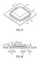
- FIGS. 1 and 2depict top and bottom plan views, respectively, of a lead frame 100 for use in a semiconductor package 200 constructed in accordance with the present invention.
- the lead frame 100comprises a frame 2 which is a substantially flat or planar plate. Located inside the frame 2 is a generally square ground ring 6 of the lead frame 100 , while located inside the ground ring 6 is a generally square, plate-like die pad or chip mounting board 8 . Formed on the inside of the frame 2 are a plurality of tie bars 4 which are connected to and support both the ground ring 6 and the chip mounting board 8 .
- a plurality of elongate slots 16which effectively separate the chip mounting board 8 and the ground ring 6 from each other by a fixed interval or gap. More particularly, four slots 16 are included in the lead frame 100 , with each defining a prescribed gap or space between each peripheral edge segments or sides of the chip mounting board 8 and a respective side or segment of the ground ring 6 . However, it will be recognized that specific areas between the chip mounting board 8 and the ground ring 6 are connected to each other via the tie bars 4 .
- the lead frame 100further comprises a plurality of leads 10 which are arranged about the periphery of the ground ring 6 .
- the leads 10are segregated into four equal sets, with each set being connected to and extending perpendicularly from a respective dambar 12 .
- the opposed ends of each dambar 12are connected to the frame 2 .
- Each dambar 12is itself connected to the distal ends of a plurality of supporting leads 14 , with the opposed ends of the supporting leads 14 themselves being connected to the frame 2 .
- the hatched portions in the drawingindicate partially etched portions of the lead frame 100 , and are described as third surfaces below.
- FIGS. 3 and 4there is depicted top and bottom plan views, respectively, of a lead frame 101 constructed in accordance with a second embodiment of the present invention.
- the lead frame 101 illustrated in FIGS. 3 and 4is substantially similar in construction to the lead frame 100 shown in FIGS. 1 and 2 , with the primary distinction being that apertures or holes 17 are formed between the chip mounting board 8 and the ground ring 6 as an alternative to the above-described slots 16 . More particularly, seven holes 17 are formed between each side of the chip mounting board 8 and the corresponding side of ground ring 6 . However, the number of holes 17 need not necessarily be restricted to seven.
- the boundary between the chip mounting board 8 and the ground ring 6is not as defined when holes 17 are employed as an alternative to the slots 16 , that portion of the lead frame 101 outside of the holes 17 is defined as the ground ring 6 in FIGS. 3 and 4 .
- the hatched portions in the drawingindicates partially etched portions of the lead frame 101 , and is also described as third surfaces below.
- the chip mounting board 8 of the lead frame 100 , 101includes a substantially flat or planar first surface 8 a .
- the chip mounting board 8defines substantially flat or planar second and third surfaces 8 b , 8 c which are opposed to the first surface 8 a .
- the third surface 8 ccircumvents the second surface 8 b , and is formed between the first and second surfaces 8 a , 8 b , i.e., the third surface 8 c is depressed (perpendicularly recessed) or partially etched in a predetermined depth relative to the second surface 8 b .
- the third surface 8 ccircumvents the second surface 8 b.
- the ground ring 6 of the lead frame 100 , 101extends about the periphery of the chip mounting board 8 and is spaced therefrom by a predetermined distance (i.e., the width of each slot 16 or diameter of each hole 17 ).
- the ground ring 6includes a substantially flat or planar first surface 6 a .
- the ground ring 6defines a substantially flat or planar second surface 6 b , and a plurality of substantially flat or planar third surfaces 6 c .
- the second and third surfaces 6 b , 6 care each opposed to the first surface 6 a , with the third surfaces 6 c being formed between the first and second surfaces 6 a , 6 b , i.e., depressed or partially etched in a predetermined depth so as to be perpendicularly recessed relative to the second surface 6 b .
- Each of the third surfaces 6 cis typically formed in a convex or concave form within the second surface 6 b .
- the ground ring 6further includes a plating layer (not shown) of a predetermined thickness applied to the first surface 6 a thereof.
- the plating layerwhich may be formed from silver or gold, provides excellent bonding with a conductive wire during a subsequent fabrication step for the semiconductor package 200 .
- a plurality of slots 16 or holes 17are disposed between the chip mounting board 8 and the ground ring 6 , though no corresponding reference numerals are included in FIGS. 5-7 .
- each of the leads 10includes a generally flat or planar first surface 10 a , and substantially flat or planar second and third surfaces 10 b , 10 c which are opposed to the first surface 10 a .
- the third surface 10 cis located at the distal end of the lead 10 closer to the ground ring 6 than the second surface 10 b .
- the third surface 10 cis formed between the first and second surfaces 10 a , 10 b , i.e., is depressed or partially etched in a predetermined depth so as to be perpendicularly recessed relative to the second surface 10 b .
- Each lead 10preferably has a plating layer of a predetermined thickness applied to the first surface 10 a thereof.
- the plating layermay comprise a metal such as silver or gold, and like the plating layer of the ground ring 6 , provides excellent bonding with a conductive wire.
- the leads 10 of the lead frame 100 , 101are each connected to a dambar 12 , with each dambar 12 being connected to the frame 2 via the supporting leads 14 .
- Each tie bar 14defines a substantially flat or planar first surface 4 a , and substantially flat or planar second and third surfaces 4 b , 4 c which are each opposed to the first surface 4 a .
- the third surface 4 cis depressed or partially etched in a predetermined depth so as to be perpendicularly recessed relative to the second surface 4 b .
- Each tie bar 4may itself include a plating layer of a predetermined thickness applied to the first surface 4 a thereof, with the plating layer being formed from metal such as silver or gold to provide superior bonding with a conductive wire as will be described in more detail below.
- the lead frame 100 , 101is manufactured by mechanically stamping or chemically etching a continuous metal strip.
- the metal stripmay be fabricated from copper, copper alloy, alloy 37 (37% nickel, 55% iron), or similar materials.
- a manufacturing method for the lead frame 100 , 101will be described in more detail below with reference to a manufacturing method for the semiconductor package 200 .
- FIGS. 8-11there is shown the semiconductor package 200 constructed in accordance with the present invention. As indicated above, FIGS. 8-10 provide cross-sectional views of the semiconductor package 200 , with a bottom plan view being shown in FIG. 11 .
- the semiconductor package 200 of the present inventionmay include either the lead frame 100 of the first embodiment or the lead frame 101 of the second embodiment. The structural attributes of the lead frame 100 , 101 are discussed above in relation to FIGS. 1-7 .
- a semiconductor chip 20 having a plurality of input-output pads 22is bonded to the first surface 8 a of the chip mounting board 8 through a layer 28 of bonding adhesive.
- the input-output pads 22 of the semiconductor chip 20 and the first surfaces 6 a , 10 a of the ground ring 6 and each lead 10 , respectively,are mechanically and electrically connected to each other through the use of conductive wires 24 .
- the conductive wires 24are each typically fabricated from gold or aluminum.
- the conductive wires 24 connected to respective ones of the leads 10are typically used for power supply or for signal transmission, with the conductive wires 24 connected to the ground ring 6 being used for grounding the semiconductor chip 20 .
- the conductive wires 24are preferably bonded only to those portions of the first surface 6 a of the ground ring 6 which are disposed in opposed relation to the second surface 6 b , i.e., those portions of the first surface 6 a which are not opposed to the third surfaces 6 b .
- the conductive wires 24are only bonded to those portions of the ground ring 6 of maximum thickness, and are not bonded to those portions of the ground ring 6 of reduced thickness attributable to the formation of the recesses defining the third surfaces 6 c therein.
- the bonding of the conductive wires 24 to only those regions of the ground ring 6 of maximum thicknessis for purposes of minimizing the bouncing phenomenon of the ground ring 6 described above during the wire bonding process.
- the chip mounting board 8 , the tie bars 4 , the ground ring 6 , the leads 10 , the semiconductor chip 20 and the conductive wires 24are all sealed with a sealing material which, when hardened, forms a sealing part 26 of the semiconductor package 200 of a specific form.
- the second surfaces 8 b , 4 b , 6 b , 10 b of the chip mounting board 8 , tie bars 4 , ground ring 6 and leads 10 , respectively,are exposed within the outer surface of the sealing part 26 .
- first surfaces 8 a , 4 a , 6 a , 10 a , the third surfaces 8 c , 4 c , 6 c , 10 c , and each of the peripheral edges or sides of the chip mounting board 8 , tie bars 4 , ground ring 6 and leads 10are located within or encapsulated by the sealing part 26 , and thus interlocked thereto.
- the second surfaces 8 b , 4 b , 6 b , 10 b of the chip mounting board 8 , tie bars 4 , ground ring 6 and leads 10 which are exposed within the sealing part 26may be mounted to an underlying substrate such as a motherboard or printed circuit board (PCB) at a later time.
- PCBprinted circuit board
- the second surfaces 8 b , 4 b , 6 b , 10 b of the chip mounting board 8 , tie bars 4 , ground ring 6 and leads 10 exposed within the sealing part 26may have a plating layer (not shown) of a predetermined thickness plated thereon, with such plating layer typically being a metal such as copper, gold, solder, tin, nickel, palladium, or others.
- the second surfaces 10 b , 6 b , 4 b of the leads 10 , ground ring 6 , and tie bars 4are mounted to a prescribed, corresponding pattern on a printed circuit board or motherboard.
- the second surface 8 b of the chip mounting board 8(which is also exposed) may also be mounted to the corresponding pattern on the motherboard through the use of a solder paste.
- the first step S 1is the step of preparing the lead frame 100 , 101 .
- the lead frames 100 , 101are each formed by chemical wet etching a metal strip.
- the chemical etchinguses photolithography, photoresist and chemical solutions for etching a pattern on the metal strip.
- a photoresist layeris formed on one side or two sides of the strip.
- the photoresist layeris exposed to light through a mask on which a desired pattern is formed.
- Chemical solutionis continuously applied to one or two sides of the strip. The exposed area of the strip is etched and removed, thus causing the desired pattern to remain on the strip.
- the lead frames 100 , 101 of the first and second embodiments of the present inventionmay be formed.
- the first etching stepis carried out on one or two sides of the strip along the photoresist pattern thereon, and by completely passing through a predetermined area of the metal strip in order to form the entire pattern on the lead frames 100 , 101 .
- a second photoresist patternis formed on a predetermined area of one side of the lead frame 100 , 101 .
- the circumferential area of the chip mounting board 8 and selected areas of the ground ring 6 , tie bars 4 , and leads 10are not wrapped by the second photoresist pattern, and therefore may be etched more by a second etching step which is carried out on one side of the lead frames 100 , 101 along the second photoresist pattern.
- the depressed surfacesare formed in the lead frames 100 , 101 , i.e., the third surface 8 c of the chip mounting board 8 , the third surfaces 6 c of the ground ring 6 , the third surface 4 c of each of the tie bars 4 , and the third surface 10 c of each of the leads 10 .
- the second etching stepis discontinued. That is, the second etching step is carried out in a manner such that the distance separating the third surface 8 c of the chip mounting board 8 from the second surface 8 b thereof, the distance separating the third surfaces 6 c of the ground ring 6 from the second surface 6 b thereof, the distance separating the third surface 4 c of each tie bar 4 from the second surface 4 b thereof, and the distance separating the third surface 10 c of each of the leads 10 from the second surface 10 b thereof allows a sufficient amount of sealing material (used to form the sealing part 26 ) to flow under the third surfaces 8 c , 6 c , 4 c , 10 c as needed to firmly secure the chip mounting board 8 , ground ring 6 , tie bars 4 and leads 10 to the sealing part 26 .
- the thickness between the first surfaces 8 a , 6 a , 4 a , 10 a and respective ones of the third surfaces 8 c , 6 c , 4 c , 10 cis in the range of from about twenty-five percent to about seventy-five percent (and preferably about fifty percent) of the thickness of the chip mounting board 8 , ground ring 6 , tie bars 4 , and leads 10 between the first surfaces 8 a , 6 a , 4 a , 10 a and respective ones of the second surfaces 8 b , 6 b , 4 b , 10 b thereof.
- the third surfaces 4 c , 6 c , 8 c , 10 cmay not be perfectly planar. Additionally, the corners defined between the second surfaces 8 b , 6 b , 4 b , 10 b and respective ones of the third surfaces 8 c , 6 c , 4 c , 10 c may not define an angle of ninety degrees, but rather may be rounded.
- the first and second etching stepsmay be changed in order, and that specific objects of the present invention may be achieved through the implementation of only the first etching step. That is, the pattern of the leads 10 may be formed by the first etching step, with the chip mounting board 8 , the ground ring 6 , the tie bars 4 and the leads 10 being etched over a prescribed thickness to form the same, and each including a stepped section.
- the lead frames 100 , 101may be formed by a first step wherein the whole pattern of the lead frames 100 , 101 is formed by stamping, followed by a second step of chemically etching the chip mounting board 8 , the ground ring 6 , the tie bars 4 , and the leads 10 of the stamped lead frame to form the depressed surfaces.
- the second step S 2 of the manufacturing methodis a chip mounting and bonding step. More particularly, the semiconductor chip 20 which includes the input-output pads 22 formed on the upper surface thereof is bonded to the approximate center of the first surface 8 a of the chip mounting board 8 through the use of a layer 28 of a bonding adhesive.
- the mounting and bonding of the semiconductor chip 20 to the chip mounting board 8may be accomplished through the use of typical semiconductor chip bonding equipment and a typical semiconductor chip bonding epoxy.
- the lead frame 100 , 101is grounded in such a manner that the same is protected from electrostatic discharge (ESD).
- the third step S 3 of the present manufacturing methodis a wire bonding step.
- each input-output pad 22 on the upper surface of the semiconductor chip 20is mechanically and electrically connected to respective ones of the first surfaces 6 a , 4 a , 10 a of the ground ring 6 , tie bars 4 and leads 10 through the use of the conductive wires 24 which, as indicated above, are typically fabricated from gold or aluminum.
- the first surfaces 6 a , 4 a , 10 acan be plated with gold, silver, nickel, palladium, copper or other metals.
- the lead frame 100 , 101is grounded to prevent a malfunction of the semiconductor chip 20 due to electrostatic discharge. Additionally, during the wire bonding process, the lead frames 100 , 101 are preferably located on an upper portion of a heat block (not shown). The second surface 6 b of the ground ring 6 remains fixed on the heat block without bouncing during the wire bonding process. Thus, the conductive wires 24 can be stably bonded to the first surface 6 a of the ground ring 6 . As indicated above, the conductive wires 24 are preferably bonded to those portions of the first surface 6 a which are disposed in opposed relation to the second surface 6 b , i.e., the surface in direct contact with the heat block.
- the conductive wires 24 mechanically and electrically connected to the ground ring 6are for ground use. That is, the ground input-output pads 22 of the semiconductor chip 20 are electrically connected to the ground ring 6 and the tie bars 4 by certain ones of the conductive wires 24 .
- the input-output pads 22 for power supply or for signal transmissionare mechanically and electrically connected to respective ones of the leads 10 by the conductive wires 24 .
- a fourth step S 4 in the present manufacturing methodis a sealing step.
- a sealing materialis applied to the lead frame 100 , 101 to form the sealing part 26 of a prescribed form.
- the sealing part 26covers the semiconductor chip 20 , the conductive wires 24 , the first and third surfaces 8 a , 8 c and peripheral edges or side surfaces of the chip mounting board 8 , the first and third surfaces 6 a , 6 c and peripheral edges or side surfaces of the ground ring 6 , the first and third surfaces 4 a , 4 c and peripheral edges or side surfaces of the tie bars 4 , and the first and third surfaces 10 a , 10 c and peripheral edges or side surfaces of the leads 10 .
- the second surfaces 8 b , 6 b , 4 b , 10 b of the chip mounting board 8 , ground ring 6 , tie bars 4 and leads 10are exposed within the outer surface of (are not covered by) the sealing part 26 .
- the sealing stepmay be performed through the use of various methodologies according to application field.
- the sealing stepcan be achieved through a general plastic sealing technique.
- the lead frame 100 , 101is located in the inside of a mold, and the sealing part 26 of the prescribed shape is formed on the upper surface of the lead frame 100 , 101 by the hardening of the sealing material injected into the mold.
- the sealing materialmay be an epoxy molding compound.
- a common gatecan be formed on the lead frame 100 , 101 to perform the sealing step smoothly.
- a side of the moldmay be tapered, so that the sealing part 26 can be easily removed from within the mold.
- An alternative sealing processcould employ the use of a liquid type sealing material. If a liquid type sealing material is to be used, a first step of the sealing process would involve the placement of the lead frame 100 , 101 onto a horizontal surface. In a second step, a common contact bead of hardenable adhesive material (e.g., a liquid-type sealing material) can be coated on the lead frame 100 , 101 to form a closed angle dam at a predetermined area of the leads 10 along the circumference of the semiconductor chip 20 . In a third step, the dam is hardened through a process such as heating at a temperature of about 140° Celsius for one hour. In a fourth step, the hardenable adhesive material is coated in the inside of the dam to form the complete sealing part. In the final step, the sealing part is hardened and formed on the lead frame 100 , 101 by heating at a temperature of about 140° Celsius for about one hour.
- a common contact bead of hardenable adhesive materiale.g., a liquid-type sealing material
- specific areas of the lead frame 100 , 101 which are not covered with the sealing part 26 and include the second surfaces 8 b , 6 b , 4 b , 10 b of the chip mounting board 8 , ground ring 6 , tie bars 4 and leads 10 , respectively,may be plated with the common plating metal which itself can be mounted to the motherboard.
- a suitable plating metalinclude gold, nickel, palladium, inconel, solder of lead and tin, or tantalum according to the application field.
- the plating stepmay be omitted if the metal used for forming the lead frame 100 , 101 does not require the plating or a pre-plating. For example, the plating step may be omitted in the event that the metal strip used for manufacturing the lead frame 100 , 101 is copper plated with nickel palladium.
- a sixth step S 6 of the present manufacturing methodis a singulation step.
- the lead frame 100 , 101 on which the sealing part 26 is formedis itself cut. That is, a specific area of each of the leads 10 which is inside of the corresponding dambar 12 is cut. The cutting is carried out by completely passing the second surface 10 b of each of the leads 10 . Furthermore, each of the tie bars 4 on the outside of the sealing part 26 is also cut. Finally, all areas which are positioned between the lead frame 100 , 101 and the sealing part 26 are removed during the singulation step.
- the singulation stepcan be carried out using a punch, a saw, or an equivalent cutting tool.
- the punch or sawcan be used in the outside of the sealing part 26 .
- the semiconductor package 200can be completely cut from the lead frame 100 , 101 by one punching motion. It is contemplated that the cutting of the leads 10 and tie bars 4 within the dambars 12 in the punching operation may occur when the lead frame 100 , 101 is turned over, i.e., flipped over from the orientation shown in FIG. 18 .
- the cutting positioncan change the cut areas of each of the leads 10 or the tie bars 4 (which each extend to side surfaces of the sealing part 26 ) from about 0.0 to about 0.5 millimeters.
- the conductive wires 24 for groundare bonded to those sections of the first surface 6 a of the ground ring 6 corresponding to the second surface 6 b , i.e., the surface in direct contact to the heat block during the wire bonding process, thereby restricting the bouncing phenomenon of the ground ring 6 during the wire bonding process. Therefore, the wire bonding is optimally performed, thereby improving the yield rate associated with the process.
- the present inventionimproves the yield rate of the wire bonding process due to the avoidance of the bouncing phenomenon as a result of not attempting to perform the wire bonding on those portions of the first surface 6 a of the ground ring 6 corresponding to (i.e., disposed in opposed relation to) the third surfaces 6 c which do not contact and are spaced from the heat block.
- the first and third surfaces 8 a , 8 c of the chip mounting board 8 , the first and third surfaces 10 a , 10 c of each of the leads 10 , and the first and third surfaces 6 a , 6 c of the ground ring 6are located inside of (are encapsulated by) the sealing part 26 , thereby improving the bonding strength between the chip mounting board 8 , leads 10 , ground ring 6 and the sealing part 26 .
- the first and third surfaces 6 a , 6 c of the ground ring 6are located inside the sealing part 26 , and the ground ring 6 is connected to the chip mounting board 8 (via the tie bars 4 ), the bonding strength between the chip mounting board 8 and the sealing part 26 is improved over semiconductor packages known in the prior art.
- the ground ring 6(as opposed to the leads 10 ) is used as the vehicle for grounding the semiconductor chip 20 , thereby having the effect of making more of the leads 10 available for processing signal from the semiconductor chip 20 .
- the input-output pads 22 of the semiconductor chip 20 for groundare all bonded not to the leads 10 , but to the ground ring 6 , thus allowing all of the leads 10 of the lead frame 100 , 101 to be used for the remaining input-output pads 22 for power supply and/or for signal transmission. Therefore, it is not necessary to manufacture the lead frame 100 , 101 as a fine-pitched lead frame or a large-sized lead frame as occurs in the prior art as explained above.
Landscapes
- Physics & Mathematics (AREA)
- Condensed Matter Physics & Semiconductors (AREA)
- General Physics & Mathematics (AREA)
- Engineering & Computer Science (AREA)
- Computer Hardware Design (AREA)
- Microelectronics & Electronic Packaging (AREA)
- Power Engineering (AREA)
- Geometry (AREA)
- Lead Frames For Integrated Circuits (AREA)
Abstract
Description
Claims (20)
Priority Applications (2)
| Application Number | Priority Date | Filing Date | Title |
|---|---|---|---|
| US12/399,600US7928542B2 (en) | 2001-03-27 | 2009-03-06 | Lead frame for semiconductor package |
| US13/036,359US8102037B2 (en) | 2001-03-27 | 2011-02-28 | Leadframe for semiconductor package |
Applications Claiming Priority (6)
| Application Number | Priority Date | Filing Date | Title |
|---|---|---|---|
| KR2001-15966 | 2001-03-27 | ||
| KR10-2001-0015966AKR100369393B1 (en) | 2001-03-27 | 2001-03-27 | Lead frame and semiconductor package using it and its manufacturing method |
| US10/013,160US6713322B2 (en) | 2001-03-27 | 2001-12-10 | Lead frame for semiconductor package |
| US10/774,893US7170150B2 (en) | 2001-03-27 | 2004-02-09 | Lead frame for semiconductor package |
| US11/510,544US7521294B2 (en) | 2001-03-27 | 2006-08-25 | Lead frame for semiconductor package |
| US12/399,600US7928542B2 (en) | 2001-03-27 | 2009-03-06 | Lead frame for semiconductor package |
Related Parent Applications (1)
| Application Number | Title | Priority Date | Filing Date |
|---|---|---|---|
| US11/510,544ContinuationUS7521294B2 (en) | 2001-03-27 | 2006-08-25 | Lead frame for semiconductor package |
Related Child Applications (1)
| Application Number | Title | Priority Date | Filing Date |
|---|---|---|---|
| US13/036,359ContinuationUS8102037B2 (en) | 2001-03-27 | 2011-02-28 | Leadframe for semiconductor package |
Publications (2)
| Publication Number | Publication Date |
|---|---|
| US20090166842A1 US20090166842A1 (en) | 2009-07-02 |
| US7928542B2true US7928542B2 (en) | 2011-04-19 |
Family
ID=19707477
Family Applications (5)
| Application Number | Title | Priority Date | Filing Date |
|---|---|---|---|
| US10/013,160Expired - LifetimeUS6713322B2 (en) | 2001-03-27 | 2001-12-10 | Lead frame for semiconductor package |
| US10/774,893Expired - LifetimeUS7170150B2 (en) | 2001-03-27 | 2004-02-09 | Lead frame for semiconductor package |
| US11/510,544Expired - LifetimeUS7521294B2 (en) | 2001-03-27 | 2006-08-25 | Lead frame for semiconductor package |
| US12/399,600Expired - Fee RelatedUS7928542B2 (en) | 2001-03-27 | 2009-03-06 | Lead frame for semiconductor package |
| US13/036,359Expired - Fee RelatedUS8102037B2 (en) | 2001-03-27 | 2011-02-28 | Leadframe for semiconductor package |
Family Applications Before (3)
| Application Number | Title | Priority Date | Filing Date |
|---|---|---|---|
| US10/013,160Expired - LifetimeUS6713322B2 (en) | 2001-03-27 | 2001-12-10 | Lead frame for semiconductor package |
| US10/774,893Expired - LifetimeUS7170150B2 (en) | 2001-03-27 | 2004-02-09 | Lead frame for semiconductor package |
| US11/510,544Expired - LifetimeUS7521294B2 (en) | 2001-03-27 | 2006-08-25 | Lead frame for semiconductor package |
Family Applications After (1)
| Application Number | Title | Priority Date | Filing Date |
|---|---|---|---|
| US13/036,359Expired - Fee RelatedUS8102037B2 (en) | 2001-03-27 | 2011-02-28 | Leadframe for semiconductor package |
Country Status (2)
| Country | Link |
|---|---|
| US (5) | US6713322B2 (en) |
| KR (1) | KR100369393B1 (en) |
Cited By (6)
| Publication number | Priority date | Publication date | Assignee | Title |
|---|---|---|---|---|
| US20120178220A1 (en)* | 2011-01-12 | 2012-07-12 | Renesas Electronics Corporation | Manufacturing method of semiconductor device |
| US9275939B1 (en)* | 2011-01-27 | 2016-03-01 | Amkor Technology, Inc. | Semiconductor device including leadframe with a combination of leads and lands and method |
| US9337140B1 (en)* | 2015-09-01 | 2016-05-10 | Freescale Semiconductor, Inc. | Signal bond wire shield |
| US9631481B1 (en)* | 2011-01-27 | 2017-04-25 | Amkor Technology, Inc. | Semiconductor device including leadframe with a combination of leads and lands and method |
| US9632487B2 (en)* | 2015-07-29 | 2017-04-25 | Lg Display Co., Ltd. | Organic light emitting display device |
| EP4383318A1 (en) | 2022-12-09 | 2024-06-12 | STMicroelectronics International N.V. | Method of manufacturing semiconductor devices, corresponding substrate and semiconductor device |
Families Citing this family (186)
| Publication number | Priority date | Publication date | Assignee | Title |
|---|---|---|---|---|
| US7071541B1 (en) | 1998-06-24 | 2006-07-04 | Amkor Technology, Inc. | Plastic integrated circuit package and method and leadframe for making the package |
| US7332375B1 (en) | 1998-06-24 | 2008-02-19 | Amkor Technology, Inc. | Method of making an integrated circuit package |
| US7005326B1 (en) | 1998-06-24 | 2006-02-28 | Amkor Technology, Inc. | Method of making an integrated circuit package |
| US6893900B1 (en) | 1998-06-24 | 2005-05-17 | Amkor Technology, Inc. | Method of making an integrated circuit package |
| US7112474B1 (en) | 1998-06-24 | 2006-09-26 | Amkor Technology, Inc. | Method of making an integrated circuit package |
| US6143981A (en) | 1998-06-24 | 2000-11-07 | Amkor Technology, Inc. | Plastic integrated circuit package and method and leadframe for making the package |
| US7030474B1 (en) | 1998-06-24 | 2006-04-18 | Amkor Technology, Inc. | Plastic integrated circuit package and method and leadframe for making the package |
| US6448633B1 (en) | 1998-11-20 | 2002-09-10 | Amkor Technology, Inc. | Semiconductor package and method of making using leadframe having lead locks to secure leads to encapsulant |
| KR100379089B1 (en) | 1999-10-15 | 2003-04-08 | 앰코 테크놀로지 코리아 주식회사 | leadframe and semiconductor package using it |
| KR20010037247A (en) | 1999-10-15 | 2001-05-07 | 마이클 디. 오브라이언 | Semiconductor package |
| KR100403142B1 (en) | 1999-10-15 | 2003-10-30 | 앰코 테크놀로지 코리아 주식회사 | semiconductor package |
| US6580159B1 (en) | 1999-11-05 | 2003-06-17 | Amkor Technology, Inc. | Integrated circuit device packages and substrates for making the packages |
| US6847103B1 (en) | 1999-11-09 | 2005-01-25 | Amkor Technology, Inc. | Semiconductor package with exposed die pad and body-locking leadframe |
| KR100421774B1 (en) | 1999-12-16 | 2004-03-10 | 앰코 테크놀로지 코리아 주식회사 | semiconductor package and its manufacturing method |
| US6639308B1 (en) | 1999-12-16 | 2003-10-28 | Amkor Technology, Inc. | Near chip size semiconductor package |
| KR100583494B1 (en) | 2000-03-25 | 2006-05-24 | 앰코 테크놀로지 코리아 주식회사 | Semiconductor Package |
| US7042068B2 (en) | 2000-04-27 | 2006-05-09 | Amkor Technology, Inc. | Leadframe and semiconductor package made using the leadframe |
| JP4417541B2 (en)* | 2000-10-23 | 2010-02-17 | ローム株式会社 | Semiconductor device and manufacturing method thereof |
| KR20020058209A (en) | 2000-12-29 | 2002-07-12 | 마이클 디. 오브라이언 | Semiconductor package |
| US6967395B1 (en) | 2001-03-20 | 2005-11-22 | Amkor Technology, Inc. | Mounting for a package containing a chip |
| US6545345B1 (en) | 2001-03-20 | 2003-04-08 | Amkor Technology, Inc. | Mounting for a package containing a chip |
| KR100393448B1 (en) | 2001-03-27 | 2003-08-02 | 앰코 테크놀로지 코리아 주식회사 | Semiconductor package and method for manufacturing the same |
| KR100369393B1 (en) | 2001-03-27 | 2003-02-05 | 앰코 테크놀로지 코리아 주식회사 | Lead frame and semiconductor package using it and its manufacturing method |
| US6597059B1 (en) | 2001-04-04 | 2003-07-22 | Amkor Technology, Inc. | Thermally enhanced chip scale lead on chip semiconductor package |
| US7064009B1 (en) | 2001-04-04 | 2006-06-20 | Amkor Technology, Inc. | Thermally enhanced chip scale lead on chip semiconductor package and method of making same |
| US7045883B1 (en) | 2001-04-04 | 2006-05-16 | Amkor Technology, Inc. | Thermally enhanced chip scale lead on chip semiconductor package and method of making same |
| US20070108609A1 (en)* | 2001-07-19 | 2007-05-17 | Samsung Electronics Co., Ltd. | Bumped chip carrier package using lead frame and method for manufacturing the same |
| KR100445072B1 (en)* | 2001-07-19 | 2004-08-21 | 삼성전자주식회사 | Bumped chip carrier package using lead frame and method for manufacturing the same |
| US7485952B1 (en) | 2001-09-19 | 2009-02-03 | Amkor Technology, Inc. | Drop resistant bumpers for fully molded memory cards |
| US6900527B1 (en) | 2001-09-19 | 2005-05-31 | Amkor Technology, Inc. | Lead-frame method and assembly for interconnecting circuits within a circuit module |
| US6630726B1 (en) | 2001-11-07 | 2003-10-07 | Amkor Technology, Inc. | Power semiconductor package with strap |
| JP4054188B2 (en)* | 2001-11-30 | 2008-02-27 | 富士通株式会社 | Semiconductor device |
| JP3939554B2 (en)* | 2002-01-15 | 2007-07-04 | シャープ株式会社 | Semiconductor lead frame |
| US6798046B1 (en)* | 2002-01-22 | 2004-09-28 | Amkor Technology, Inc. | Semiconductor package including ring structure connected to leads with vertically downset inner ends |
| EP1470587A1 (en)* | 2002-02-01 | 2004-10-27 | Infineon Technologies AG | A lead frame |
| US6838751B2 (en)* | 2002-03-06 | 2005-01-04 | Freescale Semiconductor Inc. | Multi-row leadframe |
| SG105544A1 (en)* | 2002-04-19 | 2004-08-27 | Micron Technology Inc | Ultrathin leadframe bga circuit package |
| US6818973B1 (en)* | 2002-09-09 | 2004-11-16 | Amkor Technology, Inc. | Exposed lead QFP package fabricated through the use of a partial saw process |
| US6919620B1 (en) | 2002-09-17 | 2005-07-19 | Amkor Technology, Inc. | Compact flash memory card with clamshell leadframe |
| US7135760B2 (en)* | 2002-09-30 | 2006-11-14 | St Assembly Test Services Ltd. | Moisture resistant integrated circuit leadframe package |
| US7042071B2 (en) | 2002-10-24 | 2006-05-09 | Matsushita Electric Industrial Co., Ltd. | Leadframe, plastic-encapsulated semiconductor device, and method for fabricating the same |
| US7190062B1 (en) | 2004-06-15 | 2007-03-13 | Amkor Technology, Inc. | Embedded leadframe semiconductor package |
| US7361533B1 (en) | 2002-11-08 | 2008-04-22 | Amkor Technology, Inc. | Stacked embedded leadframe |
| US6905914B1 (en) | 2002-11-08 | 2005-06-14 | Amkor Technology, Inc. | Wafer level package and fabrication method |
| US7723210B2 (en) | 2002-11-08 | 2010-05-25 | Amkor Technology, Inc. | Direct-write wafer level chip scale package |
| US8129222B2 (en)* | 2002-11-27 | 2012-03-06 | United Test And Assembly Test Center Ltd. | High density chip scale leadframe package and method of manufacturing the package |
| US20040124508A1 (en)* | 2002-11-27 | 2004-07-01 | United Test And Assembly Test Center Ltd. | High performance chip scale leadframe package and method of manufacturing the package |
| US6798047B1 (en) | 2002-12-26 | 2004-09-28 | Amkor Technology, Inc. | Pre-molded leadframe |
| SG157957A1 (en)* | 2003-01-29 | 2010-01-29 | Interplex Qlp Inc | Package for integrated circuit die |
| US6847099B1 (en) | 2003-02-05 | 2005-01-25 | Amkor Technology Inc. | Offset etched corner leads for semiconductor package |
| US6750545B1 (en) | 2003-02-28 | 2004-06-15 | Amkor Technology, Inc. | Semiconductor package capable of die stacking |
| US6927483B1 (en)* | 2003-03-07 | 2005-08-09 | Amkor Technology, Inc. | Semiconductor package exhibiting efficient lead placement |
| US7001799B1 (en) | 2003-03-13 | 2006-02-21 | Amkor Technology, Inc. | Method of making a leadframe for semiconductor devices |
| US6794740B1 (en) | 2003-03-13 | 2004-09-21 | Amkor Technology, Inc. | Leadframe package for semiconductor devices |
| US7095103B1 (en) | 2003-05-01 | 2006-08-22 | Amkor Technology, Inc. | Leadframe based memory card |
| US20040227216A1 (en)* | 2003-05-16 | 2004-11-18 | Mortan Robert F. | Flex resistant semiconductor die pad, leadframe, and package |
| US7008825B1 (en) | 2003-05-27 | 2006-03-07 | Amkor Technology, Inc. | Leadframe strip having enhanced testability |
| TWI250632B (en)* | 2003-05-28 | 2006-03-01 | Siliconware Precision Industries Co Ltd | Ground-enhancing semiconductor package and lead frame |
| CN100382295C (en)* | 2003-06-10 | 2008-04-16 | 矽品精密工业股份有限公司 | Semiconductor package capable of improving grounding quality and lead frame thereof |
| US6897550B1 (en) | 2003-06-11 | 2005-05-24 | Amkor Technology, Inc. | Fully-molded leadframe stand-off feature |
| US7049683B1 (en) | 2003-07-19 | 2006-05-23 | Ns Electronics Bangkok (1993) Ltd. | Semiconductor package including organo-metallic coating formed on surface of leadframe roughened using chemical etchant to prevent separation between leadframe and molding compound |
| KR100983304B1 (en) | 2003-08-22 | 2010-09-20 | 삼성테크윈 주식회사 | Lead frame, semiconductor package manufactured by applying same, and manufacturing method of semiconductor package |
| US7102209B1 (en)* | 2003-08-27 | 2006-09-05 | National Semiconductor Corporation | Substrate for use in semiconductor manufacturing and method of making same |
| US7245007B1 (en) | 2003-09-18 | 2007-07-17 | Amkor Technology, Inc. | Exposed lead interposer leadframe package |
| US6921967B2 (en) | 2003-09-24 | 2005-07-26 | Amkor Technology, Inc. | Reinforced die pad support structure |
| US7138707B1 (en) | 2003-10-21 | 2006-11-21 | Amkor Technology, Inc. | Semiconductor package including leads and conductive posts for providing increased functionality |
| KR100568225B1 (en)* | 2003-11-06 | 2006-04-07 | 삼성전자주식회사 | Lead frame and manufacturing method of semiconductor package using same |
| US7144517B1 (en) | 2003-11-07 | 2006-12-05 | Amkor Technology, Inc. | Manufacturing method for leadframe and for semiconductor package using the leadframe |
| US7211879B1 (en) | 2003-11-12 | 2007-05-01 | Amkor Technology, Inc. | Semiconductor package with chamfered corners and method of manufacturing the same |
| US7315077B2 (en)* | 2003-11-13 | 2008-01-01 | Fairchild Korea Semiconductor, Ltd. | Molded leadless package having a partially exposed lead frame pad |
| US7057268B1 (en) | 2004-01-27 | 2006-06-06 | Amkor Technology, Inc. | Cavity case with clip/plug for use on multi-media card |
| US7091594B1 (en) | 2004-01-28 | 2006-08-15 | Amkor Technology, Inc. | Leadframe type semiconductor package having reduced inductance and its manufacturing method |
| US7215009B1 (en)* | 2004-02-23 | 2007-05-08 | Altera Corporation | Expansion plane for PQFP/TQFP IR—package design |
| US7060536B2 (en)* | 2004-05-13 | 2006-06-13 | St Assembly Test Services Ltd. | Dual row leadframe and fabrication method |
| US8536688B2 (en)* | 2004-05-25 | 2013-09-17 | Stats Chippac Ltd. | Integrated circuit leadframe and fabrication method therefor |
| US7202554B1 (en) | 2004-08-19 | 2007-04-10 | Amkor Technology, Inc. | Semiconductor package and its manufacturing method |
| JP4525277B2 (en)* | 2004-09-30 | 2010-08-18 | ルネサスエレクトロニクス株式会社 | Semiconductor device |
| US7217991B1 (en)* | 2004-10-22 | 2007-05-15 | Amkor Technology, Inc. | Fan-in leadframe semiconductor package |
| US7387916B2 (en)* | 2004-12-02 | 2008-06-17 | Texas Instruments Incorporated | Sharp corner lead frame |
| WO2006090304A1 (en)* | 2005-02-23 | 2006-08-31 | Nxp B.V. | An integrated circuit package device with improved bond pad connections, a leadframe and an electronic device |
| TWM279015U (en)* | 2005-04-26 | 2005-10-21 | Lingsen Precision Ind Ltd | Metal leadframes for integrated circuits with different thickness of pins |
| US7504733B2 (en) | 2005-08-17 | 2009-03-17 | Ciclon Semiconductor Device Corp. | Semiconductor die package |
| US7968377B2 (en)* | 2005-09-22 | 2011-06-28 | Stats Chippac Ltd. | Integrated circuit protruding pad package system |
| US7560808B2 (en)* | 2005-10-19 | 2009-07-14 | Texas Instruments Incorporated | Chip scale power LDMOS device |
| US7507603B1 (en) | 2005-12-02 | 2009-03-24 | Amkor Technology, Inc. | Etch singulated semiconductor package |
| US7572681B1 (en) | 2005-12-08 | 2009-08-11 | Amkor Technology, Inc. | Embedded electronic component package |
| US20070132075A1 (en)* | 2005-12-12 | 2007-06-14 | Mutsumi Masumoto | Structure and method for thin single or multichip semiconductor QFN packages |
| US7446375B2 (en)* | 2006-03-14 | 2008-11-04 | Ciclon Semiconductor Device Corp. | Quasi-vertical LDMOS device having closed cell layout |
| US7816186B2 (en)* | 2006-03-14 | 2010-10-19 | Unisem (Mauritius) Holdings Limited | Method for making QFN package with power and ground rings |
| US7671463B2 (en)* | 2006-03-30 | 2010-03-02 | Stats Chippac Ltd. | Integrated circuit package system with ground ring |
| US7902660B1 (en) | 2006-05-24 | 2011-03-08 | Amkor Technology, Inc. | Substrate for semiconductor device and manufacturing method thereof |
| US7968998B1 (en) | 2006-06-21 | 2011-06-28 | Amkor Technology, Inc. | Side leaded, bottom exposed pad and bottom exposed lead fusion quad flat semiconductor package |
| US7556987B2 (en)* | 2006-06-30 | 2009-07-07 | Stats Chippac Ltd. | Method of fabricating an integrated circuit with etched ring and die paddle |
| US20080036078A1 (en)* | 2006-08-14 | 2008-02-14 | Ciclon Semiconductor Device Corp. | Wirebond-less semiconductor package |
| US8422243B2 (en)* | 2006-12-13 | 2013-04-16 | Stats Chippac Ltd. | Integrated circuit package system employing a support structure with a recess |
| US7608482B1 (en)* | 2006-12-21 | 2009-10-27 | National Semiconductor Corporation | Integrated circuit package with molded insulation |
| US8124461B2 (en)* | 2006-12-27 | 2012-02-28 | Mediatek Inc. | Method for manufacturing leadframe, packaging method for using the leadframe and semiconductor package product |
| US7834435B2 (en) | 2006-12-27 | 2010-11-16 | Mediatek Inc. | Leadframe with extended pad segments between leads and die pad, and leadframe package using the same |
| US7687893B2 (en) | 2006-12-27 | 2010-03-30 | Amkor Technology, Inc. | Semiconductor package having leadframe with exposed anchor pads |
| US8089166B2 (en)* | 2006-12-30 | 2012-01-03 | Stats Chippac Ltd. | Integrated circuit package with top pad |
| US7829990B1 (en) | 2007-01-18 | 2010-11-09 | Amkor Technology, Inc. | Stackable semiconductor package including laminate interposer |
| US20080179722A1 (en)* | 2007-01-31 | 2008-07-31 | Cyntec Co., Ltd. | Electronic package structure |
| EP2115773A4 (en)* | 2007-02-12 | 2011-11-02 | Agere Systems Inc | A quad flat no lead (qfn) integrated circuit (ic) package having a modified paddle and method for designing the package |
| US7982297B1 (en) | 2007-03-06 | 2011-07-19 | Amkor Technology, Inc. | Stackable semiconductor package having partially exposed semiconductor die and method of fabricating the same |
| TWI337387B (en)* | 2007-04-20 | 2011-02-11 | Chipmos Technologies Inc | Leadframe for leadless package, package structure and manufacturing method using the same |
| US7977774B2 (en) | 2007-07-10 | 2011-07-12 | Amkor Technology, Inc. | Fusion quad flat semiconductor package |
| US8283757B2 (en)* | 2007-07-18 | 2012-10-09 | Mediatek Inc. | Quad flat package with exposed common electrode bars |
| SG149724A1 (en)* | 2007-07-24 | 2009-02-27 | Micron Technology Inc | Semicoductor dies with recesses, associated leadframes, and associated systems and methods |
| US7687899B1 (en) | 2007-08-07 | 2010-03-30 | Amkor Technology, Inc. | Dual laminate package structure with embedded elements |
| US7777351B1 (en) | 2007-10-01 | 2010-08-17 | Amkor Technology, Inc. | Thin stacked interposer package |
| US8089159B1 (en) | 2007-10-03 | 2012-01-03 | Amkor Technology, Inc. | Semiconductor package with increased I/O density and method of making the same |
| US7847386B1 (en) | 2007-11-05 | 2010-12-07 | Amkor Technology, Inc. | Reduced size stacked semiconductor package and method of making the same |
| US7948066B2 (en)* | 2007-12-26 | 2011-05-24 | Stats Chippac Ltd. | Integrated circuit package system with lead locking structure |
| TWI385774B (en)* | 2007-12-26 | 2013-02-11 | Mediatek Inc | Lead frame package and lead frame |
| US7956453B1 (en) | 2008-01-16 | 2011-06-07 | Amkor Technology, Inc. | Semiconductor package with patterning layer and method of making same |
| US7723852B1 (en) | 2008-01-21 | 2010-05-25 | Amkor Technology, Inc. | Stacked semiconductor package and method of making same |
| US8067821B1 (en) | 2008-04-10 | 2011-11-29 | Amkor Technology, Inc. | Flat semiconductor package with half package molding |
| US7768135B1 (en) | 2008-04-17 | 2010-08-03 | Amkor Technology, Inc. | Semiconductor package with fast power-up cycle and method of making same |
| US7808084B1 (en) | 2008-05-06 | 2010-10-05 | Amkor Technology, Inc. | Semiconductor package with half-etched locking features |
| US8569872B2 (en)* | 2008-07-01 | 2013-10-29 | Stats Chippac Ltd. | Integrated circuit package system with lead-frame paddle scheme for single axis partial saw isolation |
| US8125064B1 (en) | 2008-07-28 | 2012-02-28 | Amkor Technology, Inc. | Increased I/O semiconductor package and method of making same |
| US8184453B1 (en)* | 2008-07-31 | 2012-05-22 | Amkor Technology, Inc. | Increased capacity semiconductor package |
| JP5493323B2 (en)* | 2008-09-30 | 2014-05-14 | 凸版印刷株式会社 | Manufacturing method of lead frame type substrate |
| US7847392B1 (en) | 2008-09-30 | 2010-12-07 | Amkor Technology, Inc. | Semiconductor device including leadframe with increased I/O |
| US7989933B1 (en)* | 2008-10-06 | 2011-08-02 | Amkor Technology, Inc. | Increased I/O leadframe and semiconductor device including same |
| US8008758B1 (en) | 2008-10-27 | 2011-08-30 | Amkor Technology, Inc. | Semiconductor device with increased I/O leadframe |
| US8089145B1 (en) | 2008-11-17 | 2012-01-03 | Amkor Technology, Inc. | Semiconductor device including increased capacity leadframe |
| US8072050B1 (en) | 2008-11-18 | 2011-12-06 | Amkor Technology, Inc. | Semiconductor device with increased I/O leadframe including passive device |
| US7875963B1 (en) | 2008-11-21 | 2011-01-25 | Amkor Technology, Inc. | Semiconductor device including leadframe having power bars and increased I/O |
| US7982298B1 (en) | 2008-12-03 | 2011-07-19 | Amkor Technology, Inc. | Package in package semiconductor device |
| US8487420B1 (en) | 2008-12-08 | 2013-07-16 | Amkor Technology, Inc. | Package in package semiconductor device with film over wire |
| US20170117214A1 (en) | 2009-01-05 | 2017-04-27 | Amkor Technology, Inc. | Semiconductor device with through-mold via |
| US8680656B1 (en) | 2009-01-05 | 2014-03-25 | Amkor Technology, Inc. | Leadframe structure for concentrated photovoltaic receiver package |
| US8058715B1 (en) | 2009-01-09 | 2011-11-15 | Amkor Technology, Inc. | Package in package device for RF transceiver module |
| US8049312B2 (en)* | 2009-01-12 | 2011-11-01 | Texas Instruments Incorporated | Semiconductor device package and method of assembly thereof |
| US8026589B1 (en) | 2009-02-23 | 2011-09-27 | Amkor Technology, Inc. | Reduced profile stackable semiconductor package |
| US7960818B1 (en) | 2009-03-04 | 2011-06-14 | Amkor Technology, Inc. | Conformal shield on punch QFN semiconductor package |
| US8575742B1 (en) | 2009-04-06 | 2013-11-05 | Amkor Technology, Inc. | Semiconductor device with increased I/O leadframe including power bars |
| US8383962B2 (en) | 2009-04-08 | 2013-02-26 | Marvell World Trade Ltd. | Exposed die pad package with power ring |
| US8810015B2 (en)* | 2009-06-14 | 2014-08-19 | STAT ChipPAC Ltd. | Integrated circuit packaging system with high lead count and method of manufacture thereof |
| US8551820B1 (en)* | 2009-09-28 | 2013-10-08 | Amkor Technology, Inc. | Routable single layer substrate and semiconductor package including same |
| US8796561B1 (en) | 2009-10-05 | 2014-08-05 | Amkor Technology, Inc. | Fan out build up substrate stackable package and method |
| US8937381B1 (en) | 2009-12-03 | 2015-01-20 | Amkor Technology, Inc. | Thin stackable package and method |
| US9691734B1 (en) | 2009-12-07 | 2017-06-27 | Amkor Technology, Inc. | Method of forming a plurality of electronic component packages |
| JP5255009B2 (en)* | 2010-02-26 | 2013-08-07 | ルネサスエレクトロニクス株式会社 | Semiconductor device |
| US8492887B2 (en)* | 2010-03-25 | 2013-07-23 | Stats Chippac Ltd. | Integrated circuit packaging system with leadframe and method of manufacture thereof |
| US8324511B1 (en) | 2010-04-06 | 2012-12-04 | Amkor Technology, Inc. | Through via nub reveal method and structure |
| US8294276B1 (en) | 2010-05-27 | 2012-10-23 | Amkor Technology, Inc. | Semiconductor device and fabricating method thereof |
| US8440554B1 (en) | 2010-08-02 | 2013-05-14 | Amkor Technology, Inc. | Through via connected backside embedded circuit features structure and method |
| US8409922B2 (en)* | 2010-09-14 | 2013-04-02 | Stats Chippac, Ltd. | Semiconductor device and method of forming leadframe interposer over semiconductor die and TSV substrate for vertical electrical interconnect |
| US8404524B2 (en)* | 2010-09-16 | 2013-03-26 | Stats Chippac Ltd. | Integrated circuit packaging system with paddle molding and method of manufacture thereof |
| US8487445B1 (en) | 2010-10-05 | 2013-07-16 | Amkor Technology, Inc. | Semiconductor device having through electrodes protruding from dielectric layer |
| KR101796116B1 (en) | 2010-10-20 | 2017-11-10 | 삼성전자 주식회사 | Semiconductor device, memory module and memory system having the same and operating method thereof |
| US8791501B1 (en) | 2010-12-03 | 2014-07-29 | Amkor Technology, Inc. | Integrated passive device structure and method |
| US8674485B1 (en) | 2010-12-08 | 2014-03-18 | Amkor Technology, Inc. | Semiconductor device including leadframe with downsets |
| US8377750B2 (en)* | 2010-12-14 | 2013-02-19 | Stats Chippac Ltd. | Integrated circuit packaging system with multiple row leads and method of manufacture thereof |
| US8390130B1 (en) | 2011-01-06 | 2013-03-05 | Amkor Technology, Inc. | Through via recessed reveal structure and method |
| KR101250529B1 (en)* | 2011-06-08 | 2013-04-03 | 에스티에스반도체통신 주식회사 | QFN(Quad Flat No-leads) package and the method of fabricating the same |
| US8552548B1 (en) | 2011-11-29 | 2013-10-08 | Amkor Technology, Inc. | Conductive pad on protruding through electrode semiconductor device |
| US9704725B1 (en) | 2012-03-06 | 2017-07-11 | Amkor Technology, Inc. | Semiconductor device with leadframe configured to facilitate reduced burr formation |
| US9129943B1 (en) | 2012-03-29 | 2015-09-08 | Amkor Technology, Inc. | Embedded component package and fabrication method |
| US9048298B1 (en) | 2012-03-29 | 2015-06-02 | Amkor Technology, Inc. | Backside warpage control structure and fabrication method |
| US8633575B1 (en)* | 2012-05-24 | 2014-01-21 | Amkor Technology, Inc. | IC package with integrated electrostatic discharge protection |
| KR101398016B1 (en)* | 2012-08-08 | 2014-05-30 | 앰코 테크놀로지 코리아 주식회사 | Lead frame package and manufacturing method thereof |
| DE102012215449A1 (en) | 2012-08-31 | 2014-03-27 | Osram Opto Semiconductors Gmbh | HOUSING FOR AN ELECTRONIC COMPONENT, ELECTRONIC MODULE, METHOD FOR MANUFACTURING A HOUSING FOR AN ELECTRONIC COMPONENT AND METHOD FOR PRODUCING AN ELECTRONIC MODULE |
| KR101486790B1 (en) | 2013-05-02 | 2015-01-28 | 앰코 테크놀로지 코리아 주식회사 | Micro Lead Frame for semiconductor package |
| US9000570B2 (en)* | 2013-07-11 | 2015-04-07 | Freescale Semiconductor, Inc. | Semiconductor device with corner tie bars |
| CN104425392A (en) | 2013-08-27 | 2015-03-18 | 优博创新科技有限公司 | Cavity package with pre-molded substrate |
| KR101563911B1 (en) | 2013-10-24 | 2015-10-28 | 앰코 테크놀로지 코리아 주식회사 | Semiconductor package |
| TW201539674A (en)* | 2014-04-10 | 2015-10-16 | Chipmos Technologies Inc | Quad flat no-lead package and manufacturing method thereof |
| US9673122B2 (en) | 2014-05-02 | 2017-06-06 | Amkor Technology, Inc. | Micro lead frame structure having reinforcing portions and method |
| JP6483498B2 (en)* | 2014-07-07 | 2019-03-13 | ローム株式会社 | Electronic device and its mounting structure |
| US9704785B2 (en) | 2015-01-14 | 2017-07-11 | Mediatek Inc. | Semiconductor package with die paddle |
| US9728510B2 (en) | 2015-04-10 | 2017-08-08 | Analog Devices, Inc. | Cavity package with composite substrate |
| CN106129035B (en)* | 2015-05-05 | 2021-01-29 | 恩智浦美国有限公司 | Exposed-pad integrated circuit package with mold lock |
| JP6352876B2 (en)* | 2015-09-15 | 2018-07-04 | 東芝メモリ株式会社 | Manufacturing method of semiconductor device |
| JP6603538B2 (en)* | 2015-10-23 | 2019-11-06 | 新光電気工業株式会社 | Lead frame and manufacturing method thereof |
| JP6608672B2 (en)* | 2015-10-30 | 2019-11-20 | 新光電気工業株式会社 | Semiconductor device and manufacturing method thereof, lead frame and manufacturing method thereof |
| US9966652B2 (en)* | 2015-11-03 | 2018-05-08 | Amkor Technology, Inc. | Packaged electronic device having integrated antenna and locking structure |
| CN105470234B (en)* | 2016-01-12 | 2017-12-22 | 气派科技股份有限公司 | A kind of SOT23 lead frames and its packaging technology flow |
| JP6788509B2 (en)* | 2017-01-17 | 2020-11-25 | 株式会社三井ハイテック | Lead frame manufacturing method and lead frame |
| JP1603175S (en)* | 2017-10-19 | 2018-05-07 | ||
| CN109037077B (en)* | 2018-06-13 | 2020-12-25 | 南通通富微电子有限公司 | Semiconductor chip packaging method |
| US11545418B2 (en)* | 2018-10-24 | 2023-01-03 | Texas Instruments Incorporated | Thermal capacity control for relative temperature-based thermal shutdown |
| US12046798B2 (en) | 2021-07-14 | 2024-07-23 | Amkor Technology Singapore Holding Pte. Ltd. | Semiconductor devices and methods of manufacturing semiconductor devices |
| US12317465B2 (en)* | 2022-11-29 | 2025-05-27 | Cisco Technology, Inc. | Slotted absorber |
Citations (344)
| Publication number | Priority date | Publication date | Assignee | Title |
|---|---|---|---|---|
| US2596993A (en) | 1949-01-13 | 1952-05-20 | United Shoe Machinery Corp | Method and mold for covering of eyelets by plastic injection |
| US3435815A (en) | 1966-07-15 | 1969-04-01 | Micro Tech Mfg Inc | Wafer dicer |
| US3734660A (en) | 1970-01-09 | 1973-05-22 | Tuthill Pump Co | Apparatus for fabricating a bearing device |
| US3838984A (en) | 1973-04-16 | 1974-10-01 | Sperry Rand Corp | Flexible carrier and interconnect for uncased ic chips |
| US4054238A (en) | 1976-03-23 | 1977-10-18 | Western Electric Company, Inc. | Method, apparatus and lead frame for assembling leads with terminals on a substrate |
| US4189342A (en) | 1971-10-07 | 1980-02-19 | U.S. Philips Corporation | Semiconductor device comprising projecting contact layers |
| US4221925A (en) | 1978-09-18 | 1980-09-09 | Western Electric Company, Incorporated | Printed circuit board |
| US4258381A (en) | 1977-12-07 | 1981-03-24 | Steag, Kernergie Gmbh | Lead frame for a semiconductor device suitable for mass production |
| US4289922A (en) | 1979-09-04 | 1981-09-15 | Plessey Incorporated | Integrated circuit package and lead frame |
| US4301464A (en) | 1978-08-02 | 1981-11-17 | Hitachi, Ltd. | Lead frame and semiconductor device employing the same with improved arrangement of supporting leads for securing the semiconductor supporting member |
| US4332537A (en) | 1978-07-17 | 1982-06-01 | Dusan Slepcevic | Encapsulation mold with removable cavity plates |
| US4417266A (en) | 1981-08-14 | 1983-11-22 | Amp Incorporated | Power and ground plane structure for chip carrier |
| US4451224A (en) | 1982-03-25 | 1984-05-29 | General Electric Company | Mold device for making plastic articles from resin |
| US4530152A (en) | 1982-04-01 | 1985-07-23 | Compagnie Industrielle Des Telecommunications Cit-Alcatel | Method for encapsulating semiconductor components using temporary substrates |
| US4541003A (en) | 1978-12-27 | 1985-09-10 | Hitachi, Ltd. | Semiconductor device including an alpha-particle shield |
| US4646710A (en) | 1982-09-22 | 1987-03-03 | Crystal Systems, Inc. | Multi-wafer slicing with a fixed abrasive |
| US4707724A (en) | 1984-06-04 | 1987-11-17 | Hitachi, Ltd. | Semiconductor device and method of manufacturing thereof |
| US4727633A (en) | 1985-08-08 | 1988-03-01 | Tektronix, Inc. | Method of securing metallic members together |
| US4737839A (en) | 1984-03-19 | 1988-04-12 | Trilogy Computer Development Partners, Ltd. | Semiconductor chip mounting system |
| US4756080A (en) | 1986-01-27 | 1988-07-12 | American Microsystems, Inc. | Metal foil semiconductor interconnection method |
| US4812896A (en) | 1986-11-13 | 1989-03-14 | Olin Corporation | Metal electronic package sealed with thermoplastic having a grafted metal deactivator and antioxidant |
| US4862246A (en) | 1984-09-26 | 1989-08-29 | Hitachi, Ltd. | Semiconductor device lead frame with etched through holes |
| US4862245A (en) | 1985-04-18 | 1989-08-29 | International Business Machines Corporation | Package semiconductor chip |
| US4907067A (en) | 1988-05-11 | 1990-03-06 | Texas Instruments Incorporated | Thermally efficient power device package |
| US4920074A (en) | 1987-02-25 | 1990-04-24 | Hitachi, Ltd. | Surface mount plastic package semiconductor integrated circuit, manufacturing method thereof, as well as mounting method and mounted structure thereof |
| US4935803A (en) | 1988-09-09 | 1990-06-19 | Motorola, Inc. | Self-centering electrode for power devices |
| US4942454A (en) | 1987-08-05 | 1990-07-17 | Mitsubishi Denki Kabushiki Kaisha | Resin sealed semiconductor device |
| US4987475A (en) | 1988-02-29 | 1991-01-22 | Digital Equipment Corporation | Alignment of leads for ceramic integrated circuit packages |
| US5018003A (en) | 1988-10-20 | 1991-05-21 | Mitsubishi Denki Kabushiki Kaisha | Lead frame and semiconductor device |
| US5029386A (en) | 1990-09-17 | 1991-07-09 | Hewlett-Packard Company | Hierarchical tape automated bonding method |
| US5041902A (en) | 1989-12-14 | 1991-08-20 | Motorola, Inc. | Molded electronic package with compression structures |
| US5057900A (en) | 1988-10-17 | 1991-10-15 | Semiconductor Energy Laboratory Co., Ltd. | Electronic device and a manufacturing method for the same |
| US5059379A (en) | 1987-07-20 | 1991-10-22 | Mitsubishi Denki Kabushiki Kaisha | Method of resin sealing semiconductor devices |
| US5065223A (en) | 1989-05-31 | 1991-11-12 | Fujitsu Vlsi Limited | Packaged semiconductor device |
| US5070039A (en) | 1989-04-13 | 1991-12-03 | Texas Instruments Incorporated | Method of making an integrated circuit using a pre-served dam bar to reduce mold flash and to facilitate flash removal |
| US5087961A (en) | 1987-01-28 | 1992-02-11 | Lsi Logic Corporation | Semiconductor device package |
| US5091341A (en) | 1989-05-22 | 1992-02-25 | Kabushiki Kaisha Toshiba | Method of sealing semiconductor device with resin by pressing a lead frame to a heat sink using an upper mold pressure member |
| US5096852A (en) | 1988-06-02 | 1992-03-17 | Burr-Brown Corporation | Method of making plastic encapsulated multichip hybrid integrated circuits |
| US5118298A (en) | 1991-04-04 | 1992-06-02 | Advanced Interconnections Corporation | Through hole mounting of integrated circuit adapter leads |
| US5122860A (en) | 1987-08-26 | 1992-06-16 | Matsushita Electric Industrial Co., Ltd. | Integrated circuit device and manufacturing method thereof |
| US5134773A (en) | 1989-05-26 | 1992-08-04 | Gerard Lemaire | Method for making a credit card containing a microprocessor chip |
| US5151039A (en) | 1990-04-06 | 1992-09-29 | Advanced Interconnections Corporation | Integrated circuit adapter having gullwing-shaped leads |
| US5157480A (en) | 1991-02-06 | 1992-10-20 | Motorola, Inc. | Semiconductor device having dual electrical contact sites |
| US5157475A (en) | 1988-07-08 | 1992-10-20 | Oki Electric Industry Co., Ltd. | Semiconductor device having a particular conductive lead structure |
| US5168368A (en) | 1991-05-09 | 1992-12-01 | International Business Machines Corporation | Lead frame-chip package with improved configuration |
| US5172213A (en) | 1991-05-23 | 1992-12-15 | At&T Bell Laboratories | Molded circuit package having heat dissipating post |
| US5172214A (en) | 1991-02-06 | 1992-12-15 | Motorola, Inc. | Leadless semiconductor device and method for making the same |
| US5175060A (en) | 1989-07-01 | 1992-12-29 | Ibiden Co., Ltd. | Leadframe semiconductor-mounting substrate having a roughened adhesive conductor circuit substrate and method of producing the same |
| US5200362A (en) | 1989-09-06 | 1993-04-06 | Motorola, Inc. | Method of attaching conductive traces to an encapsulated semiconductor die using a removable transfer film |
| US5200809A (en) | 1991-09-27 | 1993-04-06 | Vlsi Technology, Inc. | Exposed die-attach heatsink package |
| US5214845A (en) | 1992-05-11 | 1993-06-01 | Micron Technology, Inc. | Method for producing high speed integrated circuits |
| US5216278A (en) | 1990-12-04 | 1993-06-01 | Motorola, Inc. | Semiconductor device having a pad array carrier package |
| US5218231A (en) | 1989-08-30 | 1993-06-08 | Kabushiki Kaisha Toshiba | Mold-type semiconductor device |
| US5221642A (en) | 1991-08-15 | 1993-06-22 | Staktek Corporation | Lead-on-chip integrated circuit fabrication method |
| US5250841A (en) | 1992-04-06 | 1993-10-05 | Motorola, Inc. | Semiconductor device with test-only leads |
| US5252853A (en) | 1991-09-19 | 1993-10-12 | Mitsubishi Denki Kabushiki Kaisha | Packaged semiconductor device having tab tape and particular power distribution lead structure |
| US5258094A (en) | 1991-09-18 | 1993-11-02 | Nec Corporation | Method for producing multilayer printed wiring boards |
| US5266834A (en) | 1989-03-13 | 1993-11-30 | Hitachi Ltd. | Semiconductor device and an electronic device with the semiconductor devices mounted thereon |
| US5277972A (en) | 1988-09-29 | 1994-01-11 | Tomoegawa Paper Co., Ltd. | Adhesive tapes |
| US5278446A (en) | 1992-07-06 | 1994-01-11 | Motorola, Inc. | Reduced stress plastic package |
| US5279029A (en) | 1990-08-01 | 1994-01-18 | Staktek Corporation | Ultra high density integrated circuit packages method |
| US5281849A (en) | 1991-05-07 | 1994-01-25 | Singh Deo Narendra N | Semiconductor package with segmented lead frame |
| US5285352A (en) | 1992-07-15 | 1994-02-08 | Motorola, Inc. | Pad array semiconductor device with thermal conductor and process for making the same |
| US5294897A (en) | 1992-07-20 | 1994-03-15 | Mitsubishi Denki Kabushiki Kaisha | Microwave IC package |
| US5327008A (en) | 1993-03-22 | 1994-07-05 | Motorola Inc. | Semiconductor device having universal low-stress die support and method for making the same |
| US5332864A (en) | 1991-12-27 | 1994-07-26 | Vlsi Technology, Inc. | Integrated circuit package having an interposer |
| US5336931A (en) | 1993-09-03 | 1994-08-09 | Motorola, Inc. | Anchoring method for flow formed integrated circuit covers |
| US5335771A (en) | 1990-09-25 | 1994-08-09 | R. H. Murphy Company, Inc. | Spacer trays for stacking storage trays with integrated circuits |
| US5343076A (en) | 1990-07-21 | 1994-08-30 | Mitsui Petrochemical Industries, Ltd. | Semiconductor device with an airtight space formed internally within a hollow package |
| US5358905A (en) | 1993-04-02 | 1994-10-25 | Texas Instruments Incorporated | Semiconductor device having die pad locking to substantially reduce package cracking |
| US5365106A (en) | 1992-10-27 | 1994-11-15 | Kabushiki Kaisha Toshiba | Resin mold semiconductor device |
| US5381042A (en) | 1992-03-31 | 1995-01-10 | Amkor Electronics, Inc. | Packaged integrated circuit including heat slug having an exposed surface |
| EP0393997B1 (en) | 1989-04-20 | 1995-02-01 | Honeywell Inc. | Method of providing a variable-pitch leadframe assembly |
| US5391439A (en) | 1990-09-27 | 1995-02-21 | Dai Nippon Printing Co., Ltd. | Leadframe adapted to support semiconductor elements |
| US5406124A (en) | 1992-12-04 | 1995-04-11 | Mitsui Toatsu Chemicals, Inc. | Insulating adhesive tape, and lead frame and semiconductor device employing the tape |
| US5410180A (en) | 1992-07-28 | 1995-04-25 | Shinko Electric Industries Co., Ltd. | Metal plane support for multi-layer lead frames and a process for manufacturing such frames |
| US5414299A (en) | 1993-09-24 | 1995-05-09 | Vlsi Technology, Inc. | Semi-conductor device interconnect package assembly for improved package performance |
| US5417905A (en) | 1989-05-26 | 1995-05-23 | Esec (Far East) Limited | Method of making a card having decorations on both faces |
| US5428248A (en) | 1992-08-21 | 1995-06-27 | Goldstar Electron Co., Ltd. | Resin molded semiconductor package |
| US5435057A (en) | 1990-10-30 | 1995-07-25 | International Business Machines Corporation | Interconnection method and structure for organic circuit boards |
| US5444301A (en) | 1993-06-23 | 1995-08-22 | Goldstar Electron Co. Ltd. | Semiconductor package and method for manufacturing the same |
| US5452511A (en) | 1993-11-04 | 1995-09-26 | Chang; Alexander H. C. | Composite lead frame manufacturing method |
| US5454905A (en) | 1994-08-09 | 1995-10-03 | National Semiconductor Corporation | Method for manufacturing fine pitch lead frame |
| US5467032A (en) | 1993-11-09 | 1995-11-14 | Samsung Electronics Co., Ltd. | Word line driver circuit for a semiconductor memory device |
| US5474958A (en) | 1993-05-04 | 1995-12-12 | Motorola, Inc. | Method for making semiconductor device having no die supporting surface |
| US5484274A (en) | 1992-11-24 | 1996-01-16 | Neu Dynamics Corp. | Encapsulation molding equipment |
| US5493151A (en) | 1993-07-15 | 1996-02-20 | Kabushiki Kaisha Toshiba | Semiconductor device, lead frame and method for manufacturing semiconductor devices |
| US5508556A (en) | 1994-09-02 | 1996-04-16 | Motorola, Inc. | Leaded semiconductor device having accessible power supply pad terminals |
| US5517056A (en) | 1993-09-30 | 1996-05-14 | Motorola, Inc. | Molded carrier ring leadframe having a particular resin injecting area design for gate removal and semiconductor device employing the same |
| US5521429A (en) | 1993-11-25 | 1996-05-28 | Sanyo Electric Co., Ltd. | Surface-mount flat package semiconductor device |
| US5528076A (en) | 1995-02-01 | 1996-06-18 | Motorola, Inc. | Leadframe having metal impregnated silicon carbide mounting area |
| US5534467A (en) | 1993-03-18 | 1996-07-09 | Lsi Logic Corporation | Semiconductor packages for high I/O semiconductor dies |
| US5539251A (en) | 1992-05-11 | 1996-07-23 | Micron Technology, Inc. | Tie bar over chip lead frame design |
| US5543657A (en) | 1994-10-07 | 1996-08-06 | International Business Machines Corporation | Single layer leadframe design with groundplane capability |
| US5544412A (en) | 1994-05-24 | 1996-08-13 | Motorola, Inc. | Method for coupling a power lead to a bond pad in an electronic module |
| US5545923A (en) | 1993-10-22 | 1996-08-13 | Lsi Logic Corporation | Semiconductor device assembly with minimized bond finger connections |
| US5581122A (en) | 1994-10-25 | 1996-12-03 | Industrial Technology Research Institute | Packaging assembly with consolidated common voltage connections for integrated circuits |
| US5592019A (en) | 1994-04-19 | 1997-01-07 | Mitsubishi Denki Kabushiki Kaisha | Semiconductor device and module |
| US5592025A (en) | 1992-08-06 | 1997-01-07 | Motorola, Inc. | Pad array semiconductor device |
| US5594274A (en) | 1993-07-01 | 1997-01-14 | Nec Corporation | Lead frame for use in a semiconductor device and method of manufacturing the semiconductor device using the same |
| US5595934A (en) | 1995-05-17 | 1997-01-21 | Samsung Electronics Co., Ltd. | Method for forming oxide protective film on bonding pads of semiconductor chips by UV/O3 treatment |
| US5604376A (en) | 1994-06-30 | 1997-02-18 | Digital Equipment Corporation | Paddleless molded plastic semiconductor chip package |
| US5608267A (en) | 1992-09-17 | 1997-03-04 | Olin Corporation | Molded plastic semiconductor package including heat spreader |
| US5608265A (en) | 1993-03-17 | 1997-03-04 | Hitachi, Ltd. | Encapsulated semiconductor device package having holes for electrically conductive material |
| US5625222A (en) | 1993-11-18 | 1997-04-29 | Fujitsu Limited | Semiconductor device in a resin package housed in a frame having high thermal conductivity |
| US5633528A (en) | 1994-05-25 | 1997-05-27 | Texas Instruments Incorporated | Lead frame structure for IC devices with strengthened encapsulation adhesion |
| US5637922A (en) | 1994-02-07 | 1997-06-10 | General Electric Company | Wireless radio frequency power semiconductor devices using high density interconnect |
| US5640047A (en) | 1995-09-25 | 1997-06-17 | Mitsui High-Tec, Inc. | Ball grid assembly type semiconductor device having a heat diffusion function and an electric and magnetic shielding function |
| US5639990A (en) | 1992-06-05 | 1997-06-17 | Mitsui Toatsu Chemicals, Inc. | Solid printed substrate and electronic circuit package using the same |
| US5641997A (en) | 1993-09-14 | 1997-06-24 | Kabushiki Kaisha Toshiba | Plastic-encapsulated semiconductor device |
| US5643433A (en) | 1992-12-23 | 1997-07-01 | Shinko Electric Industries Co., Ltd. | Lead frame and method for manufacturing same |
| US5644169A (en) | 1993-03-04 | 1997-07-01 | Goldstar Electron Co., Ltd. | Mold and method for manufacturing a package for a semiconductor chip and the package manufactured thereby |
| US5646831A (en) | 1995-12-28 | 1997-07-08 | Vlsi Technology, Inc. | Electrically enhanced power quad flat pack arrangement |
| US5650663A (en) | 1995-07-03 | 1997-07-22 | Olin Corporation | Electronic package with improved thermal properties |
| US5661088A (en) | 1996-01-11 | 1997-08-26 | Motorola, Inc. | Electronic component and method of packaging |
| US5665996A (en) | 1994-12-30 | 1997-09-09 | Siliconix Incorporated | Vertical power mosfet having thick metal layer to reduce distributed resistance |
| EP0794572A2 (en) | 1996-03-07 | 1997-09-10 | Matsushita Electronics Corporation | Electronic component, method for making the same, and lead frame and mold assembly for use therein |
| US5673479A (en) | 1993-12-20 | 1997-10-07 | Lsi Logic Corporation | Method for mounting a microelectronic circuit peripherally-leaded package including integral support member with spacer |
| US5683806A (en) | 1988-09-29 | 1997-11-04 | Tomoegawa Paper Co., Ltd. | Adhesive tapes |
| US5683943A (en) | 1994-06-14 | 1997-11-04 | Dai Nippon Printing Co., Ltd. | Process for etching a semiconductor lead frame |
| US5689135A (en) | 1995-12-19 | 1997-11-18 | Micron Technology, Inc. | Multi-chip device and method of fabrication employing leads over and under processes |
| US5696666A (en) | 1995-10-11 | 1997-12-09 | Motorola, Inc. | Low profile exposed die chip carrier package |
| US5701034A (en) | 1994-05-03 | 1997-12-23 | Amkor Electronics, Inc. | Packaged semiconductor die including heat sink with locking feature |
| US5703407A (en) | 1995-02-14 | 1997-12-30 | Kabushiki Kaisha Toshiba | Resin-sealed type semiconductor device |
| US5710064A (en) | 1994-08-16 | 1998-01-20 | Samsung Electronics Co., Ltd. | Method for manufacturing a semiconductor package |
| US5724233A (en) | 1993-07-09 | 1998-03-03 | Fujitsu Limited | Semiconductor device having first and second semiconductor chips with a gap therebetween, a die stage in the gap and associated lead frames disposed in a package, the lead frames providing electrical connections from the chips to an exterior of the packag |
| US5723899A (en) | 1994-08-30 | 1998-03-03 | Amkor Electronics, Inc. | Semiconductor lead frame having connection bar and guide rings |
| US5726493A (en) | 1994-06-13 | 1998-03-10 | Fujitsu Limited | Semiconductor device and semiconductor device unit having ball-grid-array type package structure |
| US5736432A (en) | 1996-09-20 | 1998-04-07 | National Semiconductor Corporation | Lead frame with lead finger locking feature and method for making same |
| US5745984A (en) | 1995-07-10 | 1998-05-05 | Martin Marietta Corporation | Method for making an electronic module |
| US5753532A (en) | 1995-08-30 | 1998-05-19 | Samsung Electronics Co., Ltd. | Method of manufacturing semiconductor chip package |
| US5753977A (en) | 1996-03-22 | 1998-05-19 | Mitsubishi Denki Kabushiki Kaisha | Semiconductor device and lead frame therefor |
| EP0844665A2 (en) | 1996-11-21 | 1998-05-27 | Texas Instruments Incorporated | Wafer level packaging |
| US5767566A (en) | 1995-10-18 | 1998-06-16 | Kabushiki Kaisha Toshiba | Plastic mold type semiconductor device |
| US5766972A (en) | 1994-06-02 | 1998-06-16 | Mitsubishi Denki Kabushiki Kaisha | Method of making resin encapsulated semiconductor device with bump electrodes |
| US5770888A (en) | 1995-12-29 | 1998-06-23 | Lg Semicon Co., Ltd. | Integrated chip package with reduced dimensions and leads exposed from the top and bottom of the package |
| US5776798A (en) | 1996-09-04 | 1998-07-07 | Motorola, Inc. | Semiconductor package and method thereof |
| DE19734794A1 (en) | 1997-01-09 | 1998-07-16 | Mitsubishi Electric Corp | Wiring part and lead frame with the wiring part |
| US5783861A (en) | 1994-03-29 | 1998-07-21 | Lg Semicon Co., Ltd. | Semiconductor package and lead frame |
| US5801440A (en) | 1995-10-10 | 1998-09-01 | Acc Microelectronics Corporation | Chip package board having utility rings |
| US5814884A (en) | 1996-10-24 | 1998-09-29 | International Rectifier Corporation | Commonly housed diverse semiconductor die |
| US5814883A (en) | 1995-10-04 | 1998-09-29 | Mitsubishi Denki Kabushiki Kaisha | Packaged semiconductor chip |
| US5814881A (en) | 1996-12-20 | 1998-09-29 | Lsi Logic Corporation | Stacked integrated chip package and method of making same |
| US5817540A (en) | 1996-09-20 | 1998-10-06 | Micron Technology, Inc. | Method of fabricating flip-chip on leads devices and resulting assemblies |
| US5818105A (en) | 1994-07-22 | 1998-10-06 | Nec Corporation | Semiconductor device with plastic material covering a semiconductor chip mounted on a substrate of the device |
| US5821457A (en) | 1994-03-11 | 1998-10-13 | The Panda Project | Semiconductor die carrier having a dielectric epoxy between adjacent leads |
| US5821615A (en) | 1995-12-06 | 1998-10-13 | Lg Semicon Co., Ltd. | Semiconductor chip package having clip-type outlead and fabrication method of same |
| US5834830A (en) | 1995-12-18 | 1998-11-10 | Lg Semicon Co., Ltd. | LOC (lead on chip) package and fabricating method thereof |
| US5835988A (en) | 1996-03-27 | 1998-11-10 | Mitsubishi Denki Kabushiki Kaisha | Packed semiconductor device with wrap around external leads |
| US5844306A (en) | 1995-09-28 | 1998-12-01 | Mitsubishi Denki Kabushiki Kaisha | Die pad structure for solder bonding |
| US5854511A (en) | 1995-11-17 | 1998-12-29 | Anam Semiconductor, Inc. | Semiconductor package including heat sink with layered conductive plate and non-conductive tape bonding to leads |
| US5854512A (en) | 1996-09-20 | 1998-12-29 | Vlsi Technology, Inc. | High density leaded ball-grid array package |
| US5856911A (en) | 1996-11-12 | 1999-01-05 | National Semiconductor Corporation | Attachment assembly for integrated circuits |
| US5859471A (en) | 1992-11-17 | 1999-01-12 | Shinko Electric Industries Co., Ltd. | Semiconductor device having tab tape lead frame with reinforced outer leads |
| US5866939A (en) | 1996-01-21 | 1999-02-02 | Anam Semiconductor Inc. | Lead end grid array semiconductor package |
| US5866942A (en) | 1995-04-28 | 1999-02-02 | Nec Corporation | Metal base package for a semiconductor device |
| US5871782A (en) | 1995-12-30 | 1999-02-16 | Lg Semicon Co. Ltd. | Transfer molding apparatus having laminated chase block |
| US5874784A (en) | 1995-10-25 | 1999-02-23 | Sharp Kabushiki Kaisha | Semiconductor device having external connection terminals provided on an interconnection plate and fabrication process therefor |
| US5877043A (en) | 1996-02-01 | 1999-03-02 | International Business Machines Corporation | Electronic package with strain relief means and method of making |
| US5886397A (en) | 1996-09-05 | 1999-03-23 | International Rectifier Corporation | Crushable bead on lead finger side surface to improve moldability |
| KR100220154B1 (en) | 1996-04-01 | 1999-09-01 | 김규현 | Method manufacture of semiconductor package |
| US5973935A (en) | 1997-04-07 | 1999-10-26 | Micron Technology, Inc. | Interdigitated leads-over-chip lead frame for supporting an integrated circuit die |
| US5977630A (en) | 1997-08-15 | 1999-11-02 | International Rectifier Corp. | Plural semiconductor die housed in common package with split heat sink |
| JP2000150765A (en) | 1998-10-21 | 2000-05-30 | Amkor Technology Inc | Semiconductor integrated circuit plastic package, ultra- compact lead frame for manufacture thereof, and its manufacture |
| USRE36773E (en) | 1993-10-18 | 2000-07-11 | Motorola, Inc. | Method for plating using nested plating buses and semiconductor device having the same |
| US6107679A (en) | 1997-12-22 | 2000-08-22 | Oki Electric Industry Co., Ltd. | Semiconductor device |
| US6143981A (en) | 1998-06-24 | 2000-11-07 | Amkor Technology, Inc. | Plastic integrated circuit package and method and leadframe for making the package |
| KR20000072714A (en) | 2000-09-21 | 2000-12-05 | 이희영 | Mandibular angle retractor |
| US6166430A (en) | 1998-05-27 | 2000-12-26 | Matsushita Electronics Corporation | Lead frame, method for manufacturing the frame, resin-molded semiconductor device and method for manufacturing the device |
| US6169329B1 (en) | 1996-04-02 | 2001-01-02 | Micron Technology, Inc. | Semiconductor devices having interconnections using standardized bonding locations and methods of designing |
| US6177718B1 (en) | 1998-04-28 | 2001-01-23 | Kabushiki Kaisha Toshiba | Resin-sealed semiconductor device |
| US6181002B1 (en) | 1998-12-22 | 2001-01-30 | Sharp Kabushiki Kaisha | Semiconductor device having a plurality of semiconductor chips |
| US6184573B1 (en) | 1999-05-13 | 2001-02-06 | Siliconware Precision Industries Co., Ltd. | Chip packaging |
| US6184465B1 (en) | 1998-11-12 | 2001-02-06 | Micron Technology, Inc. | Semiconductor package |
| US6194777B1 (en) | 1998-06-27 | 2001-02-27 | Texas Instruments Incorporated | Leadframes with selective palladium plating |
| US6198171B1 (en) | 1999-12-30 | 2001-03-06 | Siliconware Precision Industries Co., Ltd. | Thermally enhanced quad flat non-lead package of semiconductor |
| US6197615B1 (en) | 1997-04-04 | 2001-03-06 | Samsung Electronics Co., Ltd. | Method of producing lead frame having uneven surfaces |
| US6201186B1 (en) | 1998-06-29 | 2001-03-13 | Motorola, Inc. | Electronic component assembly and method of making the same |
| US6201292B1 (en) | 1997-04-02 | 2001-03-13 | Dai Nippon Insatsu Kabushiki Kaisha | Resin-sealed semiconductor device, circuit member used therefor |
| US6204554B1 (en) | 1996-09-05 | 2001-03-20 | International Rectifier Corporation | Surface mount semiconductor package |
| US6208021B1 (en) | 1996-03-27 | 2001-03-27 | Oki Electric Industry Co., Ltd. | Semiconductor device, manufacturing method thereof and aggregate type semiconductor device |
| US6208020B1 (en) | 1999-02-24 | 2001-03-27 | Matsushita Electronics Corporation | Leadframe for use in manufacturing a resin-molded semiconductor device |
| US6208023B1 (en) | 1997-07-31 | 2001-03-27 | Matsushita Electronics Corporation | Lead frame for use with an RF powered semiconductor |
| US6211462B1 (en) | 1998-11-05 | 2001-04-03 | Texas Instruments Incorporated | Low inductance power package for integrated circuits |
| US6218731B1 (en) | 1999-05-21 | 2001-04-17 | Siliconware Precision Industries Co., Ltd. | Tiny ball grid array package |
| US6222259B1 (en) | 1998-09-15 | 2001-04-24 | Hyundai Electronics Industries Co., Ltd. | Stack package and method of fabricating the same |
| US6222258B1 (en) | 1996-11-11 | 2001-04-24 | Fujitsu Limited | Semiconductor device and method for producing a semiconductor device |
| US6225146B1 (en) | 1996-12-24 | 2001-05-01 | Matsushita Electronics Corporation | Lead frame, method of manufacturing lead frame, semiconductor device and method of manufacturing semiconductor device |
| US6229200B1 (en) | 1998-06-10 | 2001-05-08 | Asat Limited | Saw-singulated leadless plastic chip carrier |
| US6229205B1 (en) | 1997-06-30 | 2001-05-08 | Samsung Electronics Co., Ltd. | Semiconductor device package having twice-bent tie bar and small die pad |
| US6239367B1 (en) | 1999-01-29 | 2001-05-29 | United Microelectronics Corp. | Multi-chip chip scale package |
| US6239384B1 (en) | 1995-09-18 | 2001-05-29 | Tessera, Inc. | Microelectric lead structures with plural conductors |
| US6238952B1 (en) | 2000-02-29 | 2001-05-29 | Advanced Semiconductor Engineering, Inc. | Low-pin-count chip package and manufacturing method thereof |
| JP3177060B2 (en) | 1992-04-13 | 2001-06-18 | 株式会社リコー | Reversible thermosensitive recording label and card |
| US6256200B1 (en) | 1999-05-27 | 2001-07-03 | Allen K. Lam | Symmetrical package for semiconductor die |
| US6258629B1 (en) | 1999-08-09 | 2001-07-10 | Amkor Technology, Inc. | Electronic device package and leadframe and method for making the package |
| US6261864B1 (en) | 2000-01-28 | 2001-07-17 | Advanced Semiconductor Engineering, Inc. | Low-pin-count chip package and manufacturing method thereof |
| US20010008305A1 (en) | 1998-06-10 | 2001-07-19 | Asat Ltd. | Leadless plastic chip carrier with etch back pad singulation |
| US20010014538A1 (en) | 1998-06-10 | 2001-08-16 | Asat Ltd. | Leadless plastic chip carrier with etch back pad singulation and die attach pad array |
| EP0459493B1 (en) | 1990-06-01 | 2001-08-16 | Kabushiki Kaisha Toshiba | A semiconductor device comprising a TAB tape and its manufacturing method |
| US6281566B1 (en) | 1996-09-30 | 2001-08-28 | Sgs-Thomson Microelectronics S.R.L. | Plastic package for electronic devices |
| US6282094B1 (en) | 1999-04-12 | 2001-08-28 | Siliconware Precision Industries, Co., Ltd. | Ball-grid array integrated circuit package with an embedded type of heat-dissipation structure and method of manufacturing the same |
| US6282095B1 (en) | 1999-02-02 | 2001-08-28 | Compaq Computer Corporation | Method and system for controlling radio frequency radiation in microelectronic packages using heat dissipation structures |
| US6285075B1 (en) | 1998-11-02 | 2001-09-04 | Asat, Limited | Integrated circuit package with bonding planes on a ceramic ring using an adhesive assembly |
| US6291271B1 (en) | 1999-09-14 | 2001-09-18 | Advanced Semiconductor Engineering, Inc. | Method of making semiconductor chip package |
| US6291273B1 (en) | 1996-12-26 | 2001-09-18 | Hitachi, Ltd. | Plastic molded type semiconductor device and fabrication process thereof |
| US6294100B1 (en) | 1998-06-10 | 2001-09-25 | Asat Ltd | Exposed die leadless plastic chip carrier |
| US6294830B1 (en) | 1996-04-18 | 2001-09-25 | Tessera, Inc. | Microelectronic assembly with conductive terminals having an exposed surface through a dielectric layer |
| US6295977B1 (en) | 1998-11-05 | 2001-10-02 | Wacker Chemie Gmbh | Method and device for simultaneously cutting off a multiplicity of wafers from a workpiece |
| US6297548B1 (en) | 1998-06-30 | 2001-10-02 | Micron Technology, Inc. | Stackable ceramic FBGA for high thermal applications |
| US6303997B1 (en) | 1998-04-08 | 2001-10-16 | Anam Semiconductor, Inc. | Thin, stackable semiconductor packages |
| US6303984B1 (en) | 1997-08-12 | 2001-10-16 | Micron Technology, Inc. | Lead frame including angle iron tie bar |
| US6306685B1 (en) | 2000-02-01 | 2001-10-23 | Advanced Semiconductor Engineering, Inc. | Method of molding a bump chip carrier and structure made thereby |
| US6307272B1 (en) | 1998-05-27 | 2001-10-23 | Hitachi, Ltd. | Semiconductor device and method for manufacturing the same |
| US6309909B1 (en) | 1998-07-02 | 2001-10-30 | Mitsubishi Denki Kabushiki Kaisha | Semiconductor device and method of manufacturing the same |
| US6316822B1 (en) | 1998-09-16 | 2001-11-13 | Texas Instruments Incorporated | Multichip assembly semiconductor |
| US6316838B1 (en) | 1999-10-29 | 2001-11-13 | Fujitsu Limited | Semiconductor device |
| US6323550B1 (en) | 1995-06-06 | 2001-11-27 | Analog Devices, Inc. | Package for sealing an integrated circuit die |
| US6326243B1 (en) | 1995-08-15 | 2001-12-04 | Kabushiki Kaisha Toshiba | Resin sealed semiconductor device including a die pad uniformly having heat conducting paths and circulating holes for fluid resin |
| US6326244B1 (en) | 1998-09-03 | 2001-12-04 | Micron Technology, Inc. | Method of making a cavity ball grid array apparatus |
| US6326678B1 (en) | 1993-09-03 | 2001-12-04 | Asat, Limited | Molded plastic package with heat sink and enhanced electrical performance |
| US6335564B1 (en) | 1998-05-06 | 2002-01-01 | Conexant Systems, Inc. | Single Paddle having a semiconductor device and a passive electronic component |
| US6337510B1 (en) | 2000-11-17 | 2002-01-08 | Walsin Advanced Electronics Ltd | Stackable QFN semiconductor package |
| US6339255B1 (en) | 1998-10-24 | 2002-01-15 | Hyundai Electronics Industries Co., Ltd. | Stacked semiconductor chips in a single semiconductor package |
| US6342730B1 (en) | 2000-01-28 | 2002-01-29 | Advanced Semiconductor Engineering, Inc. | Low-pin-count chip package and manufacturing method thereof |
| US20020011654A1 (en) | 2000-07-25 | 2002-01-31 | Naoto Kimura | Semiconductor device |
| US6348726B1 (en)* | 2001-01-18 | 2002-02-19 | National Semiconductor Corporation | Multi row leadless leadframe package |
| US20020024122A1 (en) | 2000-08-25 | 2002-02-28 | Samsung Electronics Co., Ltd. | Lead frame having a side ring pad and semiconductor chip package including the same |
| US20020027297A1 (en) | 2000-09-04 | 2002-03-07 | Chikao Ikenaga | Semiconductor package |
| US6355502B1 (en) | 2000-04-25 | 2002-03-12 | National Science Council | Semiconductor package and method for making the same |
| US6359221B1 (en) | 1997-08-04 | 2002-03-19 | Dai Nippon Insatsu Kabushiki Kaisha | Resin sealed semiconductor device, circuit member for use therein |
| US6362525B1 (en) | 1999-11-09 | 2002-03-26 | Cypress Semiconductor Corp. | Circuit structure including a passive element formed within a grid array substrate and method for making the same |
| US20020038873A1 (en) | 2000-09-29 | 2002-04-04 | Michiaki Hiyoshi | Semiconductor device including intermediate wiring element |
| US6369447B2 (en) | 1998-04-20 | 2002-04-09 | Mitsubishi Denki Kabushiki Kaisha | Plastic-packaged semiconductor device including a plurality of chips |
| US6369454B1 (en) | 1998-12-31 | 2002-04-09 | Amkor Technology, Inc. | Semiconductor package and method for fabricating the same |
| US6373127B1 (en) | 1998-09-29 | 2002-04-16 | Texas Instruments Incorporated | Integrated capacitor on the back of a chip |
| US6377464B1 (en) | 1999-01-29 | 2002-04-23 | Conexant Systems, Inc. | Multiple chip module with integrated RF capabilities |
| US6380048B1 (en) | 2001-08-02 | 2002-04-30 | St Assembly Test Services Pte Ltd | Die paddle enhancement for exposed pad in semiconductor packaging |
| US6384472B1 (en) | 2000-03-24 | 2002-05-07 | Siliconware Precision Industries Co., Ltd | Leadless image sensor package structure and method for making the same |
| US6388336B1 (en) | 1999-09-15 | 2002-05-14 | Texas Instruments Incorporated | Multichip semiconductor assembly |
| US6395578B1 (en) | 1999-05-20 | 2002-05-28 | Amkor Technology, Inc. | Semiconductor package and method for fabricating the same |
| JP3289162B2 (en) | 1993-11-12 | 2002-06-04 | 本田技研工業株式会社 | Casting method for casting parts |
| US6400004B1 (en) | 2000-08-17 | 2002-06-04 | Advanced Semiconductor Engineering, Inc. | Leadless semiconductor package |
| US6399415B1 (en) | 2000-03-20 | 2002-06-04 | National Semiconductor Corporation | Electrical isolation in panels of leadless IC packages |
| US20020072147A1 (en) | 2000-10-24 | 2002-06-13 | Murata Manufacturing Co., Ltd. | High-frequency circuit board unit, high frequency module using the same unit, electronic apparatus using the same module, and manufacturing method for the high-frequency circuit board unit |
| US6410979B2 (en) | 1998-12-21 | 2002-06-25 | Nec Corporation | Ball-grid-array semiconductor device with protruding terminals |
| KR20020049944A (en) | 2000-12-20 | 2002-06-26 | 박종섭 | semiconductor package and method for fabricating the same |
| US6414385B1 (en) | 1999-11-08 | 2002-07-02 | Siliconware Precisionindustries Co., Ltd. | Quad flat non-lead package of semiconductor |
| US6420779B1 (en) | 1999-09-14 | 2002-07-16 | St Assembly Test Services Ltd. | Leadframe based chip scale package and method of producing the same |
| US6421013B1 (en) | 1999-10-04 | 2002-07-16 | Amerasia International Technology, Inc. | Tamper-resistant wireless article including an antenna |
| US6423643B1 (en) | 1999-10-01 | 2002-07-23 | Shinko Electric Industries Co., Ltd | Process of making carrier substrate and semiconductor device |
| US6429508B1 (en) | 2000-08-09 | 2002-08-06 | Kostat Semiconductor Co., Ltd. | Semiconductor package having implantable conductive lands and method for manufacturing the same |
| US20020111009A1 (en) | 2001-02-15 | 2002-08-15 | Megic Corporation | Reliable metal bumps on top of I/O pads after removal of test probe marks |
| US6437429B1 (en) | 2001-05-11 | 2002-08-20 | Walsin Advanced Electronics Ltd | Semiconductor package with metal pads |
| US6444499B1 (en) | 2000-03-30 | 2002-09-03 | Amkor Technology, Inc. | Method for fabricating a snapable multi-package array substrate, snapable multi-package array and snapable packaged electronic components |
| US6448633B1 (en) | 1998-11-20 | 2002-09-10 | Amkor Technology, Inc. | Semiconductor package and method of making using leadframe having lead locks to secure leads to encapsulant |
| US6452279B2 (en) | 2000-07-14 | 2002-09-17 | Mitsubishi Denki Kabushiki Kaisha | Semiconductor device |
| US6459148B1 (en) | 2000-11-13 | 2002-10-01 | Walsin Advanced Electronics Ltd | QFN semiconductor package |
| US20020140061A1 (en) | 2001-03-27 | 2002-10-03 | Lee Hyung Ju | Lead frame for semiconductor package |
| US20020140068A1 (en) | 2001-03-28 | 2002-10-03 | Ming-Hsun Lee | Leadframe-based semiconductor package for multi-media card |
| US20020140081A1 (en) | 2000-12-07 | 2002-10-03 | Young-Huang Chou | Highly integrated multi-layer circuit module having ceramic substrates with embedded passive devices |
| US6464121B2 (en) | 2000-12-21 | 2002-10-15 | Xerox Corporation | Specialized tool adapted for a process for manufacture and interconnection between adjoining printed wiring boards |
| US6465883B2 (en) | 1998-07-08 | 2002-10-15 | Telefonaktiebolaget Lm Ericsson (Publ) | Capsule for at least one high power transistor chip for high frequencies |
| US6472735B2 (en) | 2000-06-21 | 2002-10-29 | Harlan R. Isaak | Three-dimensional memory stacking using anisotropic epoxy interconnections |
| US20020158318A1 (en) | 2001-04-25 | 2002-10-31 | Chen Hung Nan | Multi-chip module |
| US6476474B1 (en) | 2000-10-10 | 2002-11-05 | Siliconware Precision Industries Co., Ltd. | Dual-die package structure and method for fabricating the same |
| US6475646B2 (en) | 2000-08-17 | 2002-11-05 | Samsung Techwin Co., Ltd. | Lead frame and method of manufacturing the lead frame |
| US6476469B2 (en) | 2000-11-23 | 2002-11-05 | Siliconware Precision Industries Co., Ltd. | Quad flat non-leaded package structure for housing CMOS sensor |
| US20020163015A1 (en) | 2001-02-27 | 2002-11-07 | Chippac, Inc. | Plastic semiconductor package |
| US20020167060A1 (en) | 2001-03-02 | 2002-11-14 | Buijsman Adrianus Alphonsus Jozef | Module and electronic device |
| US6482680B1 (en) | 2001-07-20 | 2002-11-19 | Carsem Semiconductor Sdn, Bhd. | Flip-chip on lead frame |
| US6483178B1 (en) | 2000-07-14 | 2002-11-19 | Siliconware Precision Industries Co., Ltd. | Semiconductor device package structure |
| US6492718B2 (en) | 1999-12-20 | 2002-12-10 | Kabushiki Kaisha Toshiba | Stacked semiconductor device and semiconductor system |
| US6495909B2 (en) | 2000-01-05 | 2002-12-17 | Advanced Semiconductor Engineering, Inc. | Low-pin-count chip package and manufacturing method thereof |
| US6498099B1 (en) | 1998-06-10 | 2002-12-24 | Asat Ltd. | Leadless plastic chip carrier with etch back pad singulation |
| US6498392B2 (en) | 2000-01-24 | 2002-12-24 | Nec Corporation | Semiconductor devices having different package sizes made by using common parts |
| US20030006055A1 (en) | 2001-07-05 | 2003-01-09 | Walsin Advanced Electronics Ltd | Semiconductor package for fixed surface mounting |
| US6507120B2 (en) | 2000-12-22 | 2003-01-14 | Siliconware Precision Industries Co., Ltd. | Flip chip type quad flat non-leaded package |
| US6507096B2 (en) | 2000-08-09 | 2003-01-14 | Kostat Semiconductor Co., Ltd. | Tape having implantable conductive lands for semiconductor packaging process and method for manufacturing the same |
| US6518089B2 (en) | 2001-02-02 | 2003-02-11 | Texas Instruments Incorporated | Flip chip semiconductor device in a molded chip scale package (CSP) and method of assembly |
| US20030030131A1 (en) | 2000-09-15 | 2003-02-13 | Samsung Techwin Co., Ltd., | Semiconductor package apparatus and method |
| US6525942B2 (en) | 2000-09-19 | 2003-02-25 | Siliconware Precision Industries Co., Ltd. | Heat dissipation ball grid array package |
| US20030059644A1 (en) | 2001-09-21 | 2003-03-27 | Intel Corporation | Thermo-mechanically robust C4 ball-limiting metallurgy to prevent failure due to die-package interaction and method of making same |
| US6545345B1 (en) | 2001-03-20 | 2003-04-08 | Amkor Technology, Inc. | Mounting for a package containing a chip |
| US6545332B2 (en) | 2001-01-17 | 2003-04-08 | Siliconware Precision Industries Co., Ltd. | Image sensor of a quad flat package |
| US20030073265A1 (en) | 2001-10-12 | 2003-04-17 | Tom Hu | Semiconductor package with singulation crease |
| US6552421B2 (en) | 2000-06-09 | 2003-04-22 | Hitachi, Ltd. | Semiconductor device and a method of manufacturing the same |
| US6559525B2 (en) | 2000-01-13 | 2003-05-06 | Siliconware Precision Industries Co., Ltd. | Semiconductor package having heat sink at the outer surface |
| EP0936671B1 (en) | 1998-02-12 | 2003-05-07 | Hitachi, Ltd. | Resin-moulded semiconductor hybrid module and manufacturing method thereof |
| US6580161B2 (en) | 2001-01-25 | 2003-06-17 | Rohm Co., Ltd. | Semiconductor device and method of making the same |
| US6583503B2 (en) | 1997-03-10 | 2003-06-24 | Micron Technology, Inc. | Semiconductor package with stacked substrates and multiple semiconductor dice |
| US6585905B1 (en) | 1998-06-10 | 2003-07-01 | Asat Ltd. | Leadless plastic chip carrier with partial etch die attach pad |
| JP2003243595A (en) | 2002-02-19 | 2003-08-29 | New Japan Radio Co Ltd | Semiconductor device with incorporated passive component |
| US20030164554A1 (en) | 2001-08-06 | 2003-09-04 | Fee Setho Sing | Quad flat no lead (QFN) grid array package, method of making and memory module and computer system including same |
| US20030168719A1 (en) | 2002-03-06 | 2003-09-11 | Cheng Man Hon | Multi-row leadframe |
| US6624005B1 (en) | 2000-09-06 | 2003-09-23 | Amkor Technology, Inc. | Semiconductor memory cards and method of making same |
| US6627977B1 (en) | 2002-05-09 | 2003-09-30 | Amkor Technology, Inc. | Semiconductor package including isolated ring structure |
| US20030198032A1 (en) | 2002-04-23 | 2003-10-23 | Paul Collander | Integrated circuit assembly and method for making same |
| US6646339B1 (en) | 1999-10-15 | 2003-11-11 | Amkor Technology, Inc. | Thin and heat radiant semiconductor package and method for manufacturing |
| US6667546B2 (en) | 2001-11-15 | 2003-12-23 | Siliconware Precision Industries Co., Ltd. | Ball grid array semiconductor package and substrate without power ring or ground ring |
| US6677663B1 (en) | 1999-12-30 | 2004-01-13 | Amkor Technology, Inc. | End grid array semiconductor package |
| US6686649B1 (en) | 2001-05-14 | 2004-02-03 | Amkor Technology, Inc. | Multi-chip semiconductor package with integral shield and antenna |
| US20040027788A1 (en) | 2002-08-08 | 2004-02-12 | Tz-Cheng Chiu | Polymer-embedded solder bumps for reliable plastic package attachment |
| US6696752B2 (en) | 2000-05-22 | 2004-02-24 | Siliconware Precision Industries Co., Ltd. | Encapsulated semiconductor device with flash-proof structure |
| US6700189B2 (en) | 2000-10-10 | 2004-03-02 | Rohm Co., Ltd. | Resin sealed semiconductor device |
| US20040056277A1 (en) | 2002-09-17 | 2004-03-25 | Chippac, Inc. | Semiconductor multi-package module including stacked-die package and having wire bond interconnect between stacked packages |
| US6713375B2 (en) | 1998-12-17 | 2004-03-30 | Koninklijke Philips Electronics N.V. | Method of making an electronic product including package-based inductor coupled to integrated circuit |
| US20040063246A1 (en) | 2002-09-17 | 2004-04-01 | Chippac, Inc. | Semiconductor multi-package module having package stacked over die-down flip chip ball grid array package and having wire bond interconnect between stacked packages |
| US20040061212A1 (en) | 2002-09-17 | 2004-04-01 | Chippac, Inc. | Semiconductor multi-package module having wire bond interconnect between stacked packages |
| US20040061213A1 (en) | 2002-09-17 | 2004-04-01 | Chippac, Inc. | Semiconductor multi-package module having package stacked over die-up flip chip ball grid array package and having wire bond interconnect between stacked packages |
| US20040063242A1 (en) | 2002-09-17 | 2004-04-01 | Chippac, Inc. | Semiconductor multi-package module having package stacked over ball grid array package and having wire bond interconnect between stacked packages |
| US20040065963A1 (en) | 2002-09-17 | 2004-04-08 | Chippac, Inc. | Semiconductor multi-package module having wire bond interconnect between stacked packages and having electrical shield |
| US20040080025A1 (en) | 2002-09-17 | 2004-04-29 | Shinko Electric Industries Co., Ltd. | Lead frame, method of manufacturing the same, and semiconductor device manufactured with the same |
| US20040089926A1 (en) | 2002-11-12 | 2004-05-13 | Taiwan Ic Packaging Corporation | Ultra thin semiconductor device |
| JP2004158753A (en) | 2002-11-08 | 2004-06-03 | Sony Corp | Lead frame material, manufacturing method, and semiconductor device and manufacturing method |
| US6757178B2 (en) | 2001-02-23 | 2004-06-29 | Renesas Technology Corp. | Electronic circuit equipment using multilayer circuit board |
| US20040164387A1 (en) | 2003-02-21 | 2004-08-26 | Dai Nippon Printing Co., Ltd. | Semiconductor device fabricating apparatus and semiconductor device fabricating method |
| US6800936B2 (en) | 2001-05-07 | 2004-10-05 | Sony Corporation | High-frequency module device |
| EP0720225B1 (en) | 1994-12-30 | 2004-10-27 | SILICONIX Incorporated | Lateral power MOSFET having metal strap layer to reduce distributed resistance and method of fabricating the same |
| US6812552B2 (en) | 2002-04-29 | 2004-11-02 | Advanced Interconnect Technologies Limited | Partially patterned lead frames and methods of making and using the same in semiconductor packaging |
| US6818973B1 (en) | 2002-09-09 | 2004-11-16 | Amkor Technology, Inc. | Exposed lead QFP package fabricated through the use of a partial saw process |
| US20040253803A1 (en) | 2003-06-16 | 2004-12-16 | Akira Tomono | Packaging assembly and method of assembling the same |
| US6858919B2 (en) | 2000-03-25 | 2005-02-22 | Amkor Technology, Inc. | Semiconductor package |
| US6867492B2 (en) | 2002-01-17 | 2005-03-15 | Infineon Technologies Ag | Radio-frequency power component, radio-frequency power module, method for producing a radio-frequency power component, and method for producing a radio-frequency power module |
| US6897552B2 (en) | 2001-12-12 | 2005-05-24 | Kabushiki Kaisha Toshiba | Semiconductor device wherein chips are stacked to have a fine pitch structure |
| US6927478B2 (en) | 2001-01-15 | 2005-08-09 | Amkor Technology, Inc. | Reduced size semiconductor package with stacked dies |
| US7002805B2 (en) | 2002-12-30 | 2006-02-21 | Advanced Semiconductor Engineering Inc. | Thermal enhance MCM package and manufacturing method thereof |
| US7005327B2 (en) | 2002-09-11 | 2006-02-28 | Advanced Semiconductor Engineering, Inc. | Process and structure for semiconductor package |
| US7015571B2 (en) | 2003-11-12 | 2006-03-21 | Advanced Semiconductor Engineering, Inc. | Multi-chips module assembly package |
| US20060087020A1 (en) | 2004-10-22 | 2006-04-27 | Matsushita Electric Industrial Co., Ltd. | Semiconductor device and method for producing the same |
| US7045396B2 (en) | 1999-12-16 | 2006-05-16 | Amkor Technology, Inc. | Stackable semiconductor package and method for manufacturing same |
| US7053469B2 (en) | 2004-03-30 | 2006-05-30 | Advanced Semiconductor Engineering, Inc. | Leadless semiconductor package and manufacturing method thereof |
| US20060157843A1 (en) | 2005-01-17 | 2006-07-20 | Sung-Wook Hwang | Stacked semiconductor package having interposing print circuit board |
| US7102209B1 (en) | 2003-08-27 | 2006-09-05 | National Semiconductor Corporation | Substrate for use in semiconductor manufacturing and method of making same |
| US20060216868A1 (en) | 2005-03-25 | 2006-09-28 | Advanced Semiconductor Engineering Inc. | Package structure and fabrication thereof |
| US20060231939A1 (en) | 2005-04-19 | 2006-10-19 | Takeshi Kawabata | Multilevel semiconductor module and method for fabricating the same |
| US20070023202A1 (en) | 2005-07-29 | 2007-02-01 | Sanyo Electric Co., Ltd. | Circuit board and circuit apparatus using the same |
| US7185426B1 (en) | 2002-05-01 | 2007-03-06 | Amkor Technology, Inc. | Method of manufacturing a semiconductor package |
| US7193298B2 (en) | 2002-02-01 | 2007-03-20 | Infineon Technologies Ag | Lead frame |
| US7242081B1 (en) | 2006-04-24 | 2007-07-10 | Advanced Semiconductor Engineering Inc. | Stacked package structure |
| US7245007B1 (en) | 2003-09-18 | 2007-07-17 | Amkor Technology, Inc. | Exposed lead interposer leadframe package |
| US7253503B1 (en) | 1999-11-05 | 2007-08-07 | Amkor Technology, Inc. | Integrated circuit device packages and substrates for making the packages |
| JP4098864B2 (en) | 1997-12-26 | 2008-06-11 | 東北リコー株式会社 | Paper discharge device |
| US20080230887A1 (en) | 2007-03-23 | 2008-09-25 | Advanced Semiconductor Engineering, Inc. | Semiconductor package and the method of making the same |
Family Cites Families (88)
| Publication number | Priority date | Publication date | Assignee | Title |
|---|---|---|---|---|
| JPS55163868A (en) | 1979-06-08 | 1980-12-20 | Fujitsu Ltd | Lead frame and semiconductor device using the same |
| JPS6010756Y2 (en) | 1979-06-13 | 1985-04-11 | アイダエンジニアリング株式会社 | Roll feed device |
| JPS5745959A (en) | 1980-09-02 | 1982-03-16 | Nec Corp | Resin-sealed semiconductor device |
| JPS5817705A (en) | 1981-07-23 | 1983-02-02 | Mazda Motor Corp | Antenna in common use for conductor for heating window glass of car |
| JPS58160096U (en) | 1982-04-20 | 1983-10-25 | 牧ケ谷 廣幸 | Rails for miniature car racing circuits |
| JPS6024398Y2 (en) | 1982-04-21 | 1985-07-20 | アルプス商事株式会社 | car toy |
| AU560682B2 (en) | 1982-07-13 | 1987-04-16 | Allied Corporation | Two piece chilled casting wheel |
| JPS59208756A (en) | 1983-05-12 | 1984-11-27 | Sony Corp | Manufacture of semiconductor device package |
| JPS59227143A (en) | 1983-06-07 | 1984-12-20 | Dainippon Printing Co Ltd | Package of integrated circuit |
| JPS60116239U (en) | 1984-01-12 | 1985-08-06 | 日産自動車株式会社 | Power MOSFET mounting structure |
| JPS60195957A (en) | 1984-03-19 | 1985-10-04 | Hitachi Ltd | lead frame |
| JPS60231349A (en) | 1984-05-01 | 1985-11-16 | Toshiba Corp | lead frame |
| JPS60195957U (en) | 1984-06-06 | 1985-12-27 | スズキ株式会社 | Engine intake air temperature automatic adjustment device |
| JPS6139555A (en) | 1984-07-31 | 1986-02-25 | Toshiba Corp | Resin sealed type semiconductor device with heat sink |
| JPS61248541A (en) | 1985-04-26 | 1986-11-05 | Matsushita Electronics Corp | Semiconductor device |
| JPS629639A (en) | 1985-07-05 | 1987-01-17 | Nec Yamagata Ltd | Manufacture of semiconductor device |
| JPS63205935A (en) | 1987-02-23 | 1988-08-25 | Toshiba Corp | Resin-encapsulated semiconductor device with heat sink |
| JP2509607B2 (en) | 1987-03-23 | 1996-06-26 | 株式会社東芝 | Resin-sealed semiconductor device |
| JPS63249345A (en) | 1987-04-06 | 1988-10-17 | Olympus Optical Co Ltd | Flexible mounting substrate |
| JP2548939B2 (en) | 1987-05-22 | 1996-10-30 | 大日本印刷株式会社 | Lead frame for IC card |
| JPS63188964U (en) | 1987-05-28 | 1988-12-05 | ||
| JP2656495B2 (en) | 1987-06-19 | 1997-09-24 | 株式会社フロンテック | Method for manufacturing thin film transistor |
| JPS6454749U (en) | 1987-09-30 | 1989-04-04 | ||
| JPH01106456A (en) | 1987-10-19 | 1989-04-24 | Matsushita Electric Ind Co Ltd | Semiconductor integrated circuit device |
| GB9216079D0 (en) | 1992-07-28 | 1992-09-09 | Foseco Int | Lining of molten metal handling vessel |
| JPH0692076A (en) | 1992-09-16 | 1994-04-05 | Oki Electric Ind Co Ltd | Lead frame form for ic card module |
| US5457340A (en)* | 1992-12-07 | 1995-10-10 | Integrated Device Technology, Inc. | Leadframe with power and ground planes |
| US5291061A (en) | 1993-04-06 | 1994-03-01 | Micron Semiconductor, Inc. | Multi-chip stacked devices |
| US5434057A (en)* | 1994-02-02 | 1995-07-18 | Quidel Corporation | Sperm motility assay and devices |
| JP3247384B2 (en) | 1994-03-18 | 2002-01-15 | 日立化成工業株式会社 | Semiconductor package manufacturing method and semiconductor package |
| JP3243116B2 (en) | 1994-05-17 | 2002-01-07 | 株式会社日立製作所 | Semiconductor device |
| JP3475306B2 (en) | 1994-10-26 | 2003-12-08 | 大日本印刷株式会社 | Method for manufacturing resin-encapsulated semiconductor device |
| JP3400877B2 (en) | 1994-12-14 | 2003-04-28 | 三菱電機株式会社 | Semiconductor device and manufacturing method thereof |
| JPH08306853A (en) | 1995-05-09 | 1996-11-22 | Fujitsu Ltd | Semiconductor device, method of manufacturing the same, and method of manufacturing lead frame |
| JPH098205A (en) | 1995-06-14 | 1997-01-10 | Dainippon Printing Co Ltd | Resin-sealed semiconductor device |
| JPH098206A (en) | 1995-06-19 | 1997-01-10 | Dainippon Printing Co Ltd | Lead frame and bga resin sealed semiconductor device |
| JPH098207A (en) | 1995-06-21 | 1997-01-10 | Dainippon Printing Co Ltd | Resin-sealed semiconductor device |
| JP3163961B2 (en) | 1995-09-22 | 2001-05-08 | 日立電線株式会社 | Semiconductor device |
| KR0163871B1 (en) | 1995-11-25 | 1998-12-01 | 김광호 | Solder Ball Array Package with Heat Sink Attached to Bottom |
| KR100186309B1 (en) | 1996-05-17 | 1999-03-20 | 문정환 | Stacked bottom lead package |
| US5917242A (en) | 1996-05-20 | 1999-06-29 | Micron Technology, Inc. | Combination of semiconductor interconnect |
| US5915998A (en) | 1996-06-19 | 1999-06-29 | Erico International Corporation | Electrical connector and method of making |
| JP2811170B2 (en) | 1996-06-28 | 1998-10-15 | 株式会社後藤製作所 | Resin-sealed semiconductor device and method of manufacturing the same |
| DE69735361T2 (en) | 1996-07-03 | 2006-10-19 | Seiko Epson Corp. | Resin-encapsulated semi-conductor arrangement and method of production therefor |
| KR0185512B1 (en) | 1996-08-19 | 1999-03-20 | 김광호 | Column lead type package and method of making the same |
| DE19635582C1 (en) | 1996-09-02 | 1998-02-19 | Siemens Ag | Power semiconductor component for bridge circuits with high or low side switches |
| KR100216991B1 (en) | 1996-09-11 | 1999-09-01 | 윤종용 | Leadframe having adhesive layer |
| JP3012816B2 (en) | 1996-10-22 | 2000-02-28 | 松下電子工業株式会社 | Resin-sealed semiconductor device and method of manufacturing the same |
| US6072228A (en) | 1996-10-25 | 2000-06-06 | Micron Technology, Inc. | Multi-part lead frame with dissimilar materials and method of manufacturing |
| US5981314A (en)* | 1996-10-31 | 1999-11-09 | Amkor Technology, Inc. | Near chip size integrated circuit package |
| JPH10163401A (en) | 1996-12-04 | 1998-06-19 | Sony Corp | Lead frame, semiconductor package, and manufacture of semiconductor package |
| KR100242994B1 (en) | 1996-12-28 | 2000-02-01 | 김영환 | Bottom Lead Frame and Bottom Lead Semiconductor Package Using the Same |
| JPH10256240A (en) | 1997-01-10 | 1998-09-25 | Sony Corp | Manufacture of semiconductor device |
| JPH10199934A (en) | 1997-01-13 | 1998-07-31 | Hitachi Ltd | Semiconductor element mounting structure and semiconductor element mounting method |
| US5894108A (en) | 1997-02-11 | 1999-04-13 | National Semiconductor Corporation | Plastic package with exposed die |
| JP3034814B2 (en) | 1997-02-27 | 2000-04-17 | 沖電気工業株式会社 | Lead frame structure and method of manufacturing semiconductor device |
| KR100214561B1 (en) | 1997-03-14 | 1999-08-02 | 구본준 | Rip Lead Package |
| JP2953424B2 (en) | 1997-03-31 | 1999-09-27 | 日本電気株式会社 | Lead frame for face down bonding |
| US5986885A (en) | 1997-04-08 | 1999-11-16 | Integrated Device Technology, Inc. | Semiconductor package with internal heatsink and assembly method |
| JP3022393B2 (en) | 1997-04-21 | 2000-03-21 | 日本電気株式会社 | Semiconductor device, lead frame, and method of manufacturing semiconductor device |
| JPH10303352A (en) | 1997-04-22 | 1998-11-13 | Toshiba Corp | Semiconductor device and method of manufacturing semiconductor device |
| US6113473A (en) | 1997-04-25 | 2000-09-05 | G.T. Equipment Technologies Inc. | Method and apparatus for improved wire saw slurry |
| KR19990004211A (en) | 1997-06-27 | 1999-01-15 | 한효용 | Substrate with Gate Slot |
| US6025640A (en) | 1997-07-16 | 2000-02-15 | Dai Nippon Insatsu Kabushiki Kaisha | Resin-sealed semiconductor device, circuit member for use therein and method of manufacturing resin-sealed semiconductor device |
| JP3359846B2 (en) | 1997-07-18 | 2002-12-24 | シャープ株式会社 | Semiconductor device |
| US5886398A (en) | 1997-09-26 | 1999-03-23 | Lsi Logic Corporation | Molded laminate package with integral mold gate |
| JP3644662B2 (en) | 1997-10-29 | 2005-05-11 | 株式会社ルネサステクノロジ | Semiconductor module |
| JP3481444B2 (en) | 1998-01-14 | 2003-12-22 | シャープ株式会社 | Semiconductor device and manufacturing method thereof |
| MY118338A (en) | 1998-01-26 | 2004-10-30 | Motorola Semiconductor Sdn Bhd | A leadframe, a method of manufacturing a leadframe and a method of packaging an electronic component utilising the leadframe. |
| JP3285815B2 (en) | 1998-03-12 | 2002-05-27 | 松下電器産業株式会社 | Lead frame, resin-encapsulated semiconductor device and method of manufacturing the same |
| JP3892139B2 (en) | 1998-03-27 | 2007-03-14 | 株式会社ルネサステクノロジ | Semiconductor device |
| US6130473A (en) | 1998-04-02 | 2000-10-10 | National Semiconductor Corporation | Lead frame chip scale package |
| US6034423A (en) | 1998-04-02 | 2000-03-07 | National Semiconductor Corporation | Lead frame design for increased chip pinout |
| JP3461720B2 (en) | 1998-04-20 | 2003-10-27 | 松下電器産業株式会社 | Resin-sealed semiconductor device |
| US6329224B1 (en) | 1998-04-28 | 2001-12-11 | Tessera, Inc. | Encapsulation of microelectronic assemblies |
| US5903050A (en) | 1998-04-30 | 1999-05-11 | Lsi Logic Corporation | Semiconductor package having capacitive extension spokes and method for making the same |
| KR100277438B1 (en) | 1998-05-28 | 2001-02-01 | 윤종용 | Multi Chip Package |
| KR100293815B1 (en) | 1998-06-30 | 2001-07-12 | 박종섭 | Stacked Package |
| US5951305A (en) | 1998-07-09 | 1999-09-14 | Tessera, Inc. | Lidless socket and method of making same |
| US6040626A (en) | 1998-09-25 | 2000-03-21 | International Rectifier Corp. | Semiconductor package |
| TW393744B (en) | 1998-11-10 | 2000-06-11 | Siliconware Precision Industries Co Ltd | A semicondutor packaging |
| JP4400802B2 (en) | 1999-08-23 | 2010-01-20 | 大日本印刷株式会社 | Lead frame, manufacturing method thereof, and semiconductor device |
| KR20010037254A (en)* | 1999-10-15 | 2001-05-07 | 마이클 디. 오브라이언 | Semiconductor package |
| JP2002004397A (en) | 2000-06-23 | 2002-01-09 | Kubota Corp | Pipeline construction method |
| US6611048B1 (en)* | 2000-08-25 | 2003-08-26 | Skyworks Solutions, Inc. | Exposed paddle leadframe for semiconductor die packaging |
| US6545347B2 (en)* | 2001-03-06 | 2003-04-08 | Asat, Limited | Enhanced leadless chip carrier |
| US6713311B2 (en)* | 2001-09-25 | 2004-03-30 | Texas Instruments Incorporated | Method for screening semiconductor devices for contact coplanarity |
| JP4426518B2 (en) | 2005-10-11 | 2010-03-03 | 東京エレクトロン株式会社 | Processing equipment |
- 2001
- 2001-03-27KRKR10-2001-0015966Apatent/KR100369393B1/ennot_activeExpired - Lifetime
- 2001-12-10USUS10/013,160patent/US6713322B2/ennot_activeExpired - Lifetime
- 2004
- 2004-02-09USUS10/774,893patent/US7170150B2/ennot_activeExpired - Lifetime
- 2006
- 2006-08-25USUS11/510,544patent/US7521294B2/ennot_activeExpired - Lifetime
- 2009
- 2009-03-06USUS12/399,600patent/US7928542B2/ennot_activeExpired - Fee Related
- 2011
- 2011-02-28USUS13/036,359patent/US8102037B2/ennot_activeExpired - Fee Related
Patent Citations (370)
| Publication number | Priority date | Publication date | Assignee | Title |
|---|---|---|---|---|
| US2596993A (en) | 1949-01-13 | 1952-05-20 | United Shoe Machinery Corp | Method and mold for covering of eyelets by plastic injection |
| US3435815A (en) | 1966-07-15 | 1969-04-01 | Micro Tech Mfg Inc | Wafer dicer |
| US3734660A (en) | 1970-01-09 | 1973-05-22 | Tuthill Pump Co | Apparatus for fabricating a bearing device |
| US4189342A (en) | 1971-10-07 | 1980-02-19 | U.S. Philips Corporation | Semiconductor device comprising projecting contact layers |
| US3838984A (en) | 1973-04-16 | 1974-10-01 | Sperry Rand Corp | Flexible carrier and interconnect for uncased ic chips |
| US4054238A (en) | 1976-03-23 | 1977-10-18 | Western Electric Company, Inc. | Method, apparatus and lead frame for assembling leads with terminals on a substrate |
| US4258381A (en) | 1977-12-07 | 1981-03-24 | Steag, Kernergie Gmbh | Lead frame for a semiconductor device suitable for mass production |
| US4332537A (en) | 1978-07-17 | 1982-06-01 | Dusan Slepcevic | Encapsulation mold with removable cavity plates |
| US4301464A (en) | 1978-08-02 | 1981-11-17 | Hitachi, Ltd. | Lead frame and semiconductor device employing the same with improved arrangement of supporting leads for securing the semiconductor supporting member |
| US4221925A (en) | 1978-09-18 | 1980-09-09 | Western Electric Company, Incorporated | Printed circuit board |
| US4541003A (en) | 1978-12-27 | 1985-09-10 | Hitachi, Ltd. | Semiconductor device including an alpha-particle shield |
| US4289922A (en) | 1979-09-04 | 1981-09-15 | Plessey Incorporated | Integrated circuit package and lead frame |
| US4417266A (en) | 1981-08-14 | 1983-11-22 | Amp Incorporated | Power and ground plane structure for chip carrier |
| US4451224A (en) | 1982-03-25 | 1984-05-29 | General Electric Company | Mold device for making plastic articles from resin |
| US4530152A (en) | 1982-04-01 | 1985-07-23 | Compagnie Industrielle Des Telecommunications Cit-Alcatel | Method for encapsulating semiconductor components using temporary substrates |
| US4646710A (en) | 1982-09-22 | 1987-03-03 | Crystal Systems, Inc. | Multi-wafer slicing with a fixed abrasive |
| US4737839A (en) | 1984-03-19 | 1988-04-12 | Trilogy Computer Development Partners, Ltd. | Semiconductor chip mounting system |
| US4707724A (en) | 1984-06-04 | 1987-11-17 | Hitachi, Ltd. | Semiconductor device and method of manufacturing thereof |
| US4862246A (en) | 1984-09-26 | 1989-08-29 | Hitachi, Ltd. | Semiconductor device lead frame with etched through holes |
| US4862245A (en) | 1985-04-18 | 1989-08-29 | International Business Machines Corporation | Package semiconductor chip |
| US4727633A (en) | 1985-08-08 | 1988-03-01 | Tektronix, Inc. | Method of securing metallic members together |
| US4756080A (en) | 1986-01-27 | 1988-07-12 | American Microsystems, Inc. | Metal foil semiconductor interconnection method |
| US4812896A (en) | 1986-11-13 | 1989-03-14 | Olin Corporation | Metal electronic package sealed with thermoplastic having a grafted metal deactivator and antioxidant |
| US5087961A (en) | 1987-01-28 | 1992-02-11 | Lsi Logic Corporation | Semiconductor device package |
| US4920074A (en) | 1987-02-25 | 1990-04-24 | Hitachi, Ltd. | Surface mount plastic package semiconductor integrated circuit, manufacturing method thereof, as well as mounting method and mounted structure thereof |
| US5059379A (en) | 1987-07-20 | 1991-10-22 | Mitsubishi Denki Kabushiki Kaisha | Method of resin sealing semiconductor devices |
| US4942454A (en) | 1987-08-05 | 1990-07-17 | Mitsubishi Denki Kabushiki Kaisha | Resin sealed semiconductor device |
| US5122860A (en) | 1987-08-26 | 1992-06-16 | Matsushita Electric Industrial Co., Ltd. | Integrated circuit device and manufacturing method thereof |
| US4987475A (en) | 1988-02-29 | 1991-01-22 | Digital Equipment Corporation | Alignment of leads for ceramic integrated circuit packages |
| US4907067A (en) | 1988-05-11 | 1990-03-06 | Texas Instruments Incorporated | Thermally efficient power device package |
| US5096852A (en) | 1988-06-02 | 1992-03-17 | Burr-Brown Corporation | Method of making plastic encapsulated multichip hybrid integrated circuits |
| US5157475A (en) | 1988-07-08 | 1992-10-20 | Oki Electric Industry Co., Ltd. | Semiconductor device having a particular conductive lead structure |
| US4935803A (en) | 1988-09-09 | 1990-06-19 | Motorola, Inc. | Self-centering electrode for power devices |
| US5277972A (en) | 1988-09-29 | 1994-01-11 | Tomoegawa Paper Co., Ltd. | Adhesive tapes |
| US5683806A (en) | 1988-09-29 | 1997-11-04 | Tomoegawa Paper Co., Ltd. | Adhesive tapes |
| US5277972B1 (en) | 1988-09-29 | 1996-11-05 | Tomoegawa Paper Co Ltd | Adhesive tapes |
| US5057900A (en) | 1988-10-17 | 1991-10-15 | Semiconductor Energy Laboratory Co., Ltd. | Electronic device and a manufacturing method for the same |
| US5018003A (en) | 1988-10-20 | 1991-05-21 | Mitsubishi Denki Kabushiki Kaisha | Lead frame and semiconductor device |
| US5266834A (en) | 1989-03-13 | 1993-11-30 | Hitachi Ltd. | Semiconductor device and an electronic device with the semiconductor devices mounted thereon |
| US5070039A (en) | 1989-04-13 | 1991-12-03 | Texas Instruments Incorporated | Method of making an integrated circuit using a pre-served dam bar to reduce mold flash and to facilitate flash removal |
| EP0393997B1 (en) | 1989-04-20 | 1995-02-01 | Honeywell Inc. | Method of providing a variable-pitch leadframe assembly |
| US5091341A (en) | 1989-05-22 | 1992-02-25 | Kabushiki Kaisha Toshiba | Method of sealing semiconductor device with resin by pressing a lead frame to a heat sink using an upper mold pressure member |
| US5417905A (en) | 1989-05-26 | 1995-05-23 | Esec (Far East) Limited | Method of making a card having decorations on both faces |
| US5134773A (en) | 1989-05-26 | 1992-08-04 | Gerard Lemaire | Method for making a credit card containing a microprocessor chip |
| US5065223A (en) | 1989-05-31 | 1991-11-12 | Fujitsu Vlsi Limited | Packaged semiconductor device |
| US5175060A (en) | 1989-07-01 | 1992-12-29 | Ibiden Co., Ltd. | Leadframe semiconductor-mounting substrate having a roughened adhesive conductor circuit substrate and method of producing the same |
| US5218231A (en) | 1989-08-30 | 1993-06-08 | Kabushiki Kaisha Toshiba | Mold-type semiconductor device |
| US5273938A (en) | 1989-09-06 | 1993-12-28 | Motorola, Inc. | Method for attaching conductive traces to plural, stacked, encapsulated semiconductor die using a removable transfer film |
| US5200362A (en) | 1989-09-06 | 1993-04-06 | Motorola, Inc. | Method of attaching conductive traces to an encapsulated semiconductor die using a removable transfer film |
| US5041902A (en) | 1989-12-14 | 1991-08-20 | Motorola, Inc. | Molded electronic package with compression structures |
| US5151039A (en) | 1990-04-06 | 1992-09-29 | Advanced Interconnections Corporation | Integrated circuit adapter having gullwing-shaped leads |
| EP0459493B1 (en) | 1990-06-01 | 2001-08-16 | Kabushiki Kaisha Toshiba | A semiconductor device comprising a TAB tape and its manufacturing method |
| US5343076A (en) | 1990-07-21 | 1994-08-30 | Mitsui Petrochemical Industries, Ltd. | Semiconductor device with an airtight space formed internally within a hollow package |
| US5279029A (en) | 1990-08-01 | 1994-01-18 | Staktek Corporation | Ultra high density integrated circuit packages method |
| US5029386A (en) | 1990-09-17 | 1991-07-09 | Hewlett-Packard Company | Hierarchical tape automated bonding method |
| US5335771A (en) | 1990-09-25 | 1994-08-09 | R. H. Murphy Company, Inc. | Spacer trays for stacking storage trays with integrated circuits |
| US5391439A (en) | 1990-09-27 | 1995-02-21 | Dai Nippon Printing Co., Ltd. | Leadframe adapted to support semiconductor elements |
| US5435057A (en) | 1990-10-30 | 1995-07-25 | International Business Machines Corporation | Interconnection method and structure for organic circuit boards |
| US5216278A (en) | 1990-12-04 | 1993-06-01 | Motorola, Inc. | Semiconductor device having a pad array carrier package |
| US5172214A (en) | 1991-02-06 | 1992-12-15 | Motorola, Inc. | Leadless semiconductor device and method for making the same |
| US5157480A (en) | 1991-02-06 | 1992-10-20 | Motorola, Inc. | Semiconductor device having dual electrical contact sites |
| US5118298A (en) | 1991-04-04 | 1992-06-02 | Advanced Interconnections Corporation | Through hole mounting of integrated circuit adapter leads |
| US5281849A (en) | 1991-05-07 | 1994-01-25 | Singh Deo Narendra N | Semiconductor package with segmented lead frame |
| US5168368A (en) | 1991-05-09 | 1992-12-01 | International Business Machines Corporation | Lead frame-chip package with improved configuration |
| US5172213A (en) | 1991-05-23 | 1992-12-15 | At&T Bell Laboratories | Molded circuit package having heat dissipating post |
| US5221642A (en) | 1991-08-15 | 1993-06-22 | Staktek Corporation | Lead-on-chip integrated circuit fabrication method |
| US5258094A (en) | 1991-09-18 | 1993-11-02 | Nec Corporation | Method for producing multilayer printed wiring boards |
| US5252853A (en) | 1991-09-19 | 1993-10-12 | Mitsubishi Denki Kabushiki Kaisha | Packaged semiconductor device having tab tape and particular power distribution lead structure |
| US5200809A (en) | 1991-09-27 | 1993-04-06 | Vlsi Technology, Inc. | Exposed die-attach heatsink package |
| US5332864A (en) | 1991-12-27 | 1994-07-26 | Vlsi Technology, Inc. | Integrated circuit package having an interposer |
| US5381042A (en) | 1992-03-31 | 1995-01-10 | Amkor Electronics, Inc. | Packaged integrated circuit including heat slug having an exposed surface |
| US5250841A (en) | 1992-04-06 | 1993-10-05 | Motorola, Inc. | Semiconductor device with test-only leads |
| JP3177060B2 (en) | 1992-04-13 | 2001-06-18 | 株式会社リコー | Reversible thermosensitive recording label and card |
| US5214845A (en) | 1992-05-11 | 1993-06-01 | Micron Technology, Inc. | Method for producing high speed integrated circuits |
| US5539251A (en) | 1992-05-11 | 1996-07-23 | Micron Technology, Inc. | Tie bar over chip lead frame design |
| US5639990A (en) | 1992-06-05 | 1997-06-17 | Mitsui Toatsu Chemicals, Inc. | Solid printed substrate and electronic circuit package using the same |
| US5278446A (en) | 1992-07-06 | 1994-01-11 | Motorola, Inc. | Reduced stress plastic package |
| US5285352A (en) | 1992-07-15 | 1994-02-08 | Motorola, Inc. | Pad array semiconductor device with thermal conductor and process for making the same |
| US5294897A (en) | 1992-07-20 | 1994-03-15 | Mitsubishi Denki Kabushiki Kaisha | Microwave IC package |
| US5410180A (en) | 1992-07-28 | 1995-04-25 | Shinko Electric Industries Co., Ltd. | Metal plane support for multi-layer lead frames and a process for manufacturing such frames |
| US5592025A (en) | 1992-08-06 | 1997-01-07 | Motorola, Inc. | Pad array semiconductor device |
| US5428248A (en) | 1992-08-21 | 1995-06-27 | Goldstar Electron Co., Ltd. | Resin molded semiconductor package |
| US5608267A (en) | 1992-09-17 | 1997-03-04 | Olin Corporation | Molded plastic semiconductor package including heat spreader |
| US5365106A (en) | 1992-10-27 | 1994-11-15 | Kabushiki Kaisha Toshiba | Resin mold semiconductor device |
| US5859471A (en) | 1992-11-17 | 1999-01-12 | Shinko Electric Industries Co., Ltd. | Semiconductor device having tab tape lead frame with reinforced outer leads |
| US5484274A (en) | 1992-11-24 | 1996-01-16 | Neu Dynamics Corp. | Encapsulation molding equipment |
| US5406124A (en) | 1992-12-04 | 1995-04-11 | Mitsui Toatsu Chemicals, Inc. | Insulating adhesive tape, and lead frame and semiconductor device employing the tape |
| US5643433A (en) | 1992-12-23 | 1997-07-01 | Shinko Electric Industries Co., Ltd. | Lead frame and method for manufacturing same |
| US5644169A (en) | 1993-03-04 | 1997-07-01 | Goldstar Electron Co., Ltd. | Mold and method for manufacturing a package for a semiconductor chip and the package manufactured thereby |
| US5608265A (en) | 1993-03-17 | 1997-03-04 | Hitachi, Ltd. | Encapsulated semiconductor device package having holes for electrically conductive material |
| US5534467A (en) | 1993-03-18 | 1996-07-09 | Lsi Logic Corporation | Semiconductor packages for high I/O semiconductor dies |
| US5327008A (en) | 1993-03-22 | 1994-07-05 | Motorola Inc. | Semiconductor device having universal low-stress die support and method for making the same |
| US5424576A (en) | 1993-03-22 | 1995-06-13 | Motorola, Inc. | Semiconductor device having x-shaped die support member and method for making the same |
| US5358905A (en) | 1993-04-02 | 1994-10-25 | Texas Instruments Incorporated | Semiconductor device having die pad locking to substantially reduce package cracking |
| US5474958A (en) | 1993-05-04 | 1995-12-12 | Motorola, Inc. | Method for making semiconductor device having no die supporting surface |
| US5444301A (en) | 1993-06-23 | 1995-08-22 | Goldstar Electron Co. Ltd. | Semiconductor package and method for manufacturing the same |
| US5594274A (en) | 1993-07-01 | 1997-01-14 | Nec Corporation | Lead frame for use in a semiconductor device and method of manufacturing the semiconductor device using the same |
| US5724233A (en) | 1993-07-09 | 1998-03-03 | Fujitsu Limited | Semiconductor device having first and second semiconductor chips with a gap therebetween, a die stage in the gap and associated lead frames disposed in a package, the lead frames providing electrical connections from the chips to an exterior of the packag |
| US5493151A (en) | 1993-07-15 | 1996-02-20 | Kabushiki Kaisha Toshiba | Semiconductor device, lead frame and method for manufacturing semiconductor devices |
| US6326678B1 (en) | 1993-09-03 | 2001-12-04 | Asat, Limited | Molded plastic package with heat sink and enhanced electrical performance |
| US5336931A (en) | 1993-09-03 | 1994-08-09 | Motorola, Inc. | Anchoring method for flow formed integrated circuit covers |
| US5641997A (en) | 1993-09-14 | 1997-06-24 | Kabushiki Kaisha Toshiba | Plastic-encapsulated semiconductor device |
| US5414299A (en) | 1993-09-24 | 1995-05-09 | Vlsi Technology, Inc. | Semi-conductor device interconnect package assembly for improved package performance |
| US5517056A (en) | 1993-09-30 | 1996-05-14 | Motorola, Inc. | Molded carrier ring leadframe having a particular resin injecting area design for gate removal and semiconductor device employing the same |
| USRE36773E (en) | 1993-10-18 | 2000-07-11 | Motorola, Inc. | Method for plating using nested plating buses and semiconductor device having the same |
| US5545923A (en) | 1993-10-22 | 1996-08-13 | Lsi Logic Corporation | Semiconductor device assembly with minimized bond finger connections |
| US5452511A (en) | 1993-11-04 | 1995-09-26 | Chang; Alexander H. C. | Composite lead frame manufacturing method |
| US5467032A (en) | 1993-11-09 | 1995-11-14 | Samsung Electronics Co., Ltd. | Word line driver circuit for a semiconductor memory device |
| JP3289162B2 (en) | 1993-11-12 | 2002-06-04 | 本田技研工業株式会社 | Casting method for casting parts |
| US5625222A (en) | 1993-11-18 | 1997-04-29 | Fujitsu Limited | Semiconductor device in a resin package housed in a frame having high thermal conductivity |
| US5521429A (en) | 1993-11-25 | 1996-05-28 | Sanyo Electric Co., Ltd. | Surface-mount flat package semiconductor device |
| US5673479A (en) | 1993-12-20 | 1997-10-07 | Lsi Logic Corporation | Method for mounting a microelectronic circuit peripherally-leaded package including integral support member with spacer |
| US5637922A (en) | 1994-02-07 | 1997-06-10 | General Electric Company | Wireless radio frequency power semiconductor devices using high density interconnect |
| US5821457A (en) | 1994-03-11 | 1998-10-13 | The Panda Project | Semiconductor die carrier having a dielectric epoxy between adjacent leads |
| US5783861A (en) | 1994-03-29 | 1998-07-21 | Lg Semicon Co., Ltd. | Semiconductor package and lead frame |
| US5592019A (en) | 1994-04-19 | 1997-01-07 | Mitsubishi Denki Kabushiki Kaisha | Semiconductor device and module |
| US5701034A (en) | 1994-05-03 | 1997-12-23 | Amkor Electronics, Inc. | Packaged semiconductor die including heat sink with locking feature |
| US5544412A (en) | 1994-05-24 | 1996-08-13 | Motorola, Inc. | Method for coupling a power lead to a bond pad in an electronic module |
| US5633528A (en) | 1994-05-25 | 1997-05-27 | Texas Instruments Incorporated | Lead frame structure for IC devices with strengthened encapsulation adhesion |
| US5766972A (en) | 1994-06-02 | 1998-06-16 | Mitsubishi Denki Kabushiki Kaisha | Method of making resin encapsulated semiconductor device with bump electrodes |
| US5726493A (en) | 1994-06-13 | 1998-03-10 | Fujitsu Limited | Semiconductor device and semiconductor device unit having ball-grid-array type package structure |
| US5683943A (en) | 1994-06-14 | 1997-11-04 | Dai Nippon Printing Co., Ltd. | Process for etching a semiconductor lead frame |
| US5604376A (en) | 1994-06-30 | 1997-02-18 | Digital Equipment Corporation | Paddleless molded plastic semiconductor chip package |
| US5818105A (en) | 1994-07-22 | 1998-10-06 | Nec Corporation | Semiconductor device with plastic material covering a semiconductor chip mounted on a substrate of the device |
| US5454905A (en) | 1994-08-09 | 1995-10-03 | National Semiconductor Corporation | Method for manufacturing fine pitch lead frame |
| US5710064A (en) | 1994-08-16 | 1998-01-20 | Samsung Electronics Co., Ltd. | Method for manufacturing a semiconductor package |
| US5723899A (en) | 1994-08-30 | 1998-03-03 | Amkor Electronics, Inc. | Semiconductor lead frame having connection bar and guide rings |
| US5508556A (en) | 1994-09-02 | 1996-04-16 | Motorola, Inc. | Leaded semiconductor device having accessible power supply pad terminals |
| US5814877A (en) | 1994-10-07 | 1998-09-29 | International Business Machines Corporation | Single layer leadframe design with groundplane capability |
| US5543657A (en) | 1994-10-07 | 1996-08-06 | International Business Machines Corporation | Single layer leadframe design with groundplane capability |
| US5581122A (en) | 1994-10-25 | 1996-12-03 | Industrial Technology Research Institute | Packaging assembly with consolidated common voltage connections for integrated circuits |
| EP0720225B1 (en) | 1994-12-30 | 2004-10-27 | SILICONIX Incorporated | Lateral power MOSFET having metal strap layer to reduce distributed resistance and method of fabricating the same |
| US5665996A (en) | 1994-12-30 | 1997-09-09 | Siliconix Incorporated | Vertical power mosfet having thick metal layer to reduce distributed resistance |
| EP0720234B1 (en) | 1994-12-30 | 2006-03-08 | SILICONIX Incorporated | Vertical power MOSFET having thick metal layer to reduce distributed resistance and method of fabricating the same |
| US5528076A (en) | 1995-02-01 | 1996-06-18 | Motorola, Inc. | Leadframe having metal impregnated silicon carbide mounting area |
| US5703407A (en) | 1995-02-14 | 1997-12-30 | Kabushiki Kaisha Toshiba | Resin-sealed type semiconductor device |
| US5866942A (en) | 1995-04-28 | 1999-02-02 | Nec Corporation | Metal base package for a semiconductor device |
| US5595934A (en) | 1995-05-17 | 1997-01-21 | Samsung Electronics Co., Ltd. | Method for forming oxide protective film on bonding pads of semiconductor chips by UV/O3 treatment |
| US6323550B1 (en) | 1995-06-06 | 2001-11-27 | Analog Devices, Inc. | Package for sealing an integrated circuit die |
| US5650663A (en) | 1995-07-03 | 1997-07-22 | Olin Corporation | Electronic package with improved thermal properties |
| US5745984A (en) | 1995-07-10 | 1998-05-05 | Martin Marietta Corporation | Method for making an electronic module |
| US6326243B1 (en) | 1995-08-15 | 2001-12-04 | Kabushiki Kaisha Toshiba | Resin sealed semiconductor device including a die pad uniformly having heat conducting paths and circulating holes for fluid resin |
| US5753532A (en) | 1995-08-30 | 1998-05-19 | Samsung Electronics Co., Ltd. | Method of manufacturing semiconductor chip package |
| US6239384B1 (en) | 1995-09-18 | 2001-05-29 | Tessera, Inc. | Microelectric lead structures with plural conductors |
| US5640047A (en) | 1995-09-25 | 1997-06-17 | Mitsui High-Tec, Inc. | Ball grid assembly type semiconductor device having a heat diffusion function and an electric and magnetic shielding function |
| US5844306A (en) | 1995-09-28 | 1998-12-01 | Mitsubishi Denki Kabushiki Kaisha | Die pad structure for solder bonding |
| US5814883A (en) | 1995-10-04 | 1998-09-29 | Mitsubishi Denki Kabushiki Kaisha | Packaged semiconductor chip |
| US5801440A (en) | 1995-10-10 | 1998-09-01 | Acc Microelectronics Corporation | Chip package board having utility rings |
| US5696666A (en) | 1995-10-11 | 1997-12-09 | Motorola, Inc. | Low profile exposed die chip carrier package |
| US5767566A (en) | 1995-10-18 | 1998-06-16 | Kabushiki Kaisha Toshiba | Plastic mold type semiconductor device |
| US5874784A (en) | 1995-10-25 | 1999-02-23 | Sharp Kabushiki Kaisha | Semiconductor device having external connection terminals provided on an interconnection plate and fabrication process therefor |
| US5854511A (en) | 1995-11-17 | 1998-12-29 | Anam Semiconductor, Inc. | Semiconductor package including heat sink with layered conductive plate and non-conductive tape bonding to leads |
| US5821615A (en) | 1995-12-06 | 1998-10-13 | Lg Semicon Co., Ltd. | Semiconductor chip package having clip-type outlead and fabrication method of same |
| US5834830A (en) | 1995-12-18 | 1998-11-10 | Lg Semicon Co., Ltd. | LOC (lead on chip) package and fabricating method thereof |
| US5689135A (en) | 1995-12-19 | 1997-11-18 | Micron Technology, Inc. | Multi-chip device and method of fabrication employing leads over and under processes |
| US5646831A (en) | 1995-12-28 | 1997-07-08 | Vlsi Technology, Inc. | Electrically enhanced power quad flat pack arrangement |
| US5770888A (en) | 1995-12-29 | 1998-06-23 | Lg Semicon Co., Ltd. | Integrated chip package with reduced dimensions and leads exposed from the top and bottom of the package |
| US5871782A (en) | 1995-12-30 | 1999-02-16 | Lg Semicon Co. Ltd. | Transfer molding apparatus having laminated chase block |
| US5661088A (en) | 1996-01-11 | 1997-08-26 | Motorola, Inc. | Electronic component and method of packaging |
| US5866939A (en) | 1996-01-21 | 1999-02-02 | Anam Semiconductor Inc. | Lead end grid array semiconductor package |
| US5877043A (en) | 1996-02-01 | 1999-03-02 | International Business Machines Corporation | Electronic package with strain relief means and method of making |
| EP0794572A2 (en) | 1996-03-07 | 1997-09-10 | Matsushita Electronics Corporation | Electronic component, method for making the same, and lead frame and mold assembly for use therein |
| US5753977A (en) | 1996-03-22 | 1998-05-19 | Mitsubishi Denki Kabushiki Kaisha | Semiconductor device and lead frame therefor |
| US6208021B1 (en) | 1996-03-27 | 2001-03-27 | Oki Electric Industry Co., Ltd. | Semiconductor device, manufacturing method thereof and aggregate type semiconductor device |
| US5835988A (en) | 1996-03-27 | 1998-11-10 | Mitsubishi Denki Kabushiki Kaisha | Packed semiconductor device with wrap around external leads |
| KR100220154B1 (en) | 1996-04-01 | 1999-09-01 | 김규현 | Method manufacture of semiconductor package |
| US6169329B1 (en) | 1996-04-02 | 2001-01-02 | Micron Technology, Inc. | Semiconductor devices having interconnections using standardized bonding locations and methods of designing |
| US6294830B1 (en) | 1996-04-18 | 2001-09-25 | Tessera, Inc. | Microelectronic assembly with conductive terminals having an exposed surface through a dielectric layer |
| US6150709A (en) | 1996-06-21 | 2000-11-21 | Anam Semiconductor Inc. | Grid array type lead frame having lead ends in different planes |
| US5776798A (en) | 1996-09-04 | 1998-07-07 | Motorola, Inc. | Semiconductor package and method thereof |
| US5886397A (en) | 1996-09-05 | 1999-03-23 | International Rectifier Corporation | Crushable bead on lead finger side surface to improve moldability |
| US6204554B1 (en) | 1996-09-05 | 2001-03-20 | International Rectifier Corporation | Surface mount semiconductor package |
| US5736432A (en) | 1996-09-20 | 1998-04-07 | National Semiconductor Corporation | Lead frame with lead finger locking feature and method for making same |
| US5817540A (en) | 1996-09-20 | 1998-10-06 | Micron Technology, Inc. | Method of fabricating flip-chip on leads devices and resulting assemblies |
| US5854512A (en) | 1996-09-20 | 1998-12-29 | Vlsi Technology, Inc. | High density leaded ball-grid array package |
| US6281566B1 (en) | 1996-09-30 | 2001-08-28 | Sgs-Thomson Microelectronics S.R.L. | Plastic package for electronic devices |
| US5814884A (en) | 1996-10-24 | 1998-09-29 | International Rectifier Corporation | Commonly housed diverse semiconductor die |
| US5814884C1 (en) | 1996-10-24 | 2002-01-29 | Int Rectifier Corp | Commonly housed diverse semiconductor die |
| US6222258B1 (en) | 1996-11-11 | 2001-04-24 | Fujitsu Limited | Semiconductor device and method for producing a semiconductor device |
| US5856911A (en) | 1996-11-12 | 1999-01-05 | National Semiconductor Corporation | Attachment assembly for integrated circuits |
| EP0844665A2 (en) | 1996-11-21 | 1998-05-27 | Texas Instruments Incorporated | Wafer level packaging |
| US5814881A (en) | 1996-12-20 | 1998-09-29 | Lsi Logic Corporation | Stacked integrated chip package and method of making same |
| US6225146B1 (en) | 1996-12-24 | 2001-05-01 | Matsushita Electronics Corporation | Lead frame, method of manufacturing lead frame, semiconductor device and method of manufacturing semiconductor device |
| US6291273B1 (en) | 1996-12-26 | 2001-09-18 | Hitachi, Ltd. | Plastic molded type semiconductor device and fabrication process thereof |
| DE19734794A1 (en) | 1997-01-09 | 1998-07-16 | Mitsubishi Electric Corp | Wiring part and lead frame with the wiring part |
| US6583503B2 (en) | 1997-03-10 | 2003-06-24 | Micron Technology, Inc. | Semiconductor package with stacked substrates and multiple semiconductor dice |
| US6201292B1 (en) | 1997-04-02 | 2001-03-13 | Dai Nippon Insatsu Kabushiki Kaisha | Resin-sealed semiconductor device, circuit member used therefor |
| US6197615B1 (en) | 1997-04-04 | 2001-03-06 | Samsung Electronics Co., Ltd. | Method of producing lead frame having uneven surfaces |
| US5973935A (en) | 1997-04-07 | 1999-10-26 | Micron Technology, Inc. | Interdigitated leads-over-chip lead frame for supporting an integrated circuit die |
| US6229205B1 (en) | 1997-06-30 | 2001-05-08 | Samsung Electronics Co., Ltd. | Semiconductor device package having twice-bent tie bar and small die pad |
| US6208023B1 (en) | 1997-07-31 | 2001-03-27 | Matsushita Electronics Corporation | Lead frame for use with an RF powered semiconductor |
| US6359221B1 (en) | 1997-08-04 | 2002-03-19 | Dai Nippon Insatsu Kabushiki Kaisha | Resin sealed semiconductor device, circuit member for use therein |
| US6303984B1 (en) | 1997-08-12 | 2001-10-16 | Micron Technology, Inc. | Lead frame including angle iron tie bar |
| US5977630A (en) | 1997-08-15 | 1999-11-02 | International Rectifier Corp. | Plural semiconductor die housed in common package with split heat sink |
| US6107679A (en) | 1997-12-22 | 2000-08-22 | Oki Electric Industry Co., Ltd. | Semiconductor device |
| JP4098864B2 (en) | 1997-12-26 | 2008-06-11 | 東北リコー株式会社 | Paper discharge device |
| EP0936671B1 (en) | 1998-02-12 | 2003-05-07 | Hitachi, Ltd. | Resin-moulded semiconductor hybrid module and manufacturing method thereof |
| US6303997B1 (en) | 1998-04-08 | 2001-10-16 | Anam Semiconductor, Inc. | Thin, stackable semiconductor packages |
| US6369447B2 (en) | 1998-04-20 | 2002-04-09 | Mitsubishi Denki Kabushiki Kaisha | Plastic-packaged semiconductor device including a plurality of chips |
| US6177718B1 (en) | 1998-04-28 | 2001-01-23 | Kabushiki Kaisha Toshiba | Resin-sealed semiconductor device |
| US6335564B1 (en) | 1998-05-06 | 2002-01-01 | Conexant Systems, Inc. | Single Paddle having a semiconductor device and a passive electronic component |
| US6307272B1 (en) | 1998-05-27 | 2001-10-23 | Hitachi, Ltd. | Semiconductor device and method for manufacturing the same |
| US6166430A (en) | 1998-05-27 | 2000-12-26 | Matsushita Electronics Corporation | Lead frame, method for manufacturing the frame, resin-molded semiconductor device and method for manufacturing the device |
| US6242281B1 (en) | 1998-06-10 | 2001-06-05 | Asat, Limited | Saw-singulated leadless plastic chip carrier |
| US20030102537A1 (en) | 1998-06-10 | 2003-06-05 | Mclellan Neil | Saw singulated leadless plastic chip carrier |
| US20010014538A1 (en) | 1998-06-10 | 2001-08-16 | Asat Ltd. | Leadless plastic chip carrier with etch back pad singulation and die attach pad array |
| US6229200B1 (en) | 1998-06-10 | 2001-05-08 | Asat Limited | Saw-singulated leadless plastic chip carrier |
| US6585905B1 (en) | 1998-06-10 | 2003-07-01 | Asat Ltd. | Leadless plastic chip carrier with partial etch die attach pad |
| US20010008305A1 (en) | 1998-06-10 | 2001-07-19 | Asat Ltd. | Leadless plastic chip carrier with etch back pad singulation |
| US6498099B1 (en) | 1998-06-10 | 2002-12-24 | Asat Ltd. | Leadless plastic chip carrier with etch back pad singulation |
| US6294100B1 (en) | 1998-06-10 | 2001-09-25 | Asat Ltd | Exposed die leadless plastic chip carrier |
| US6143981A (en) | 1998-06-24 | 2000-11-07 | Amkor Technology, Inc. | Plastic integrated circuit package and method and leadframe for making the package |
| JP2002519848A (en) | 1998-06-24 | 2002-07-02 | アムコール・テクノロジー・インコーポレイテッド | Integrated circuit plastic package, method of forming the same, and lead frame for forming the package |
| US6194777B1 (en) | 1998-06-27 | 2001-02-27 | Texas Instruments Incorporated | Leadframes with selective palladium plating |
| US6201186B1 (en) | 1998-06-29 | 2001-03-13 | Motorola, Inc. | Electronic component assembly and method of making the same |
| US6297548B1 (en) | 1998-06-30 | 2001-10-02 | Micron Technology, Inc. | Stackable ceramic FBGA for high thermal applications |
| US6309909B1 (en) | 1998-07-02 | 2001-10-30 | Mitsubishi Denki Kabushiki Kaisha | Semiconductor device and method of manufacturing the same |
| US6465883B2 (en) | 1998-07-08 | 2002-10-15 | Telefonaktiebolaget Lm Ericsson (Publ) | Capsule for at least one high power transistor chip for high frequencies |
| US6326244B1 (en) | 1998-09-03 | 2001-12-04 | Micron Technology, Inc. | Method of making a cavity ball grid array apparatus |
| US6222259B1 (en) | 1998-09-15 | 2001-04-24 | Hyundai Electronics Industries Co., Ltd. | Stack package and method of fabricating the same |
| US6316822B1 (en) | 1998-09-16 | 2001-11-13 | Texas Instruments Incorporated | Multichip assembly semiconductor |
| EP0989608A3 (en) | 1998-09-21 | 2001-01-10 | Amkor Technology Inc. | Plastic integrated circuit device package and method of making the same |
| US6373127B1 (en) | 1998-09-29 | 2002-04-16 | Texas Instruments Incorporated | Integrated capacitor on the back of a chip |
| JP2000150765A (en) | 1998-10-21 | 2000-05-30 | Amkor Technology Inc | Semiconductor integrated circuit plastic package, ultra- compact lead frame for manufacture thereof, and its manufacture |
| US6281568B1 (en) | 1998-10-21 | 2001-08-28 | Amkor Technology, Inc. | Plastic integrated circuit device package and leadframe having partially undercut leads and die pad |
| US6339255B1 (en) | 1998-10-24 | 2002-01-15 | Hyundai Electronics Industries Co., Ltd. | Stacked semiconductor chips in a single semiconductor package |
| US6285075B1 (en) | 1998-11-02 | 2001-09-04 | Asat, Limited | Integrated circuit package with bonding planes on a ceramic ring using an adhesive assembly |
| US6211462B1 (en) | 1998-11-05 | 2001-04-03 | Texas Instruments Incorporated | Low inductance power package for integrated circuits |
| US6295977B1 (en) | 1998-11-05 | 2001-10-02 | Wacker Chemie Gmbh | Method and device for simultaneously cutting off a multiplicity of wafers from a workpiece |
| US6184465B1 (en) | 1998-11-12 | 2001-02-06 | Micron Technology, Inc. | Semiconductor package |
| US6448633B1 (en) | 1998-11-20 | 2002-09-10 | Amkor Technology, Inc. | Semiconductor package and method of making using leadframe having lead locks to secure leads to encapsulant |
| US6713375B2 (en) | 1998-12-17 | 2004-03-30 | Koninklijke Philips Electronics N.V. | Method of making an electronic product including package-based inductor coupled to integrated circuit |
| US6410979B2 (en) | 1998-12-21 | 2002-06-25 | Nec Corporation | Ball-grid-array semiconductor device with protruding terminals |
| US6181002B1 (en) | 1998-12-22 | 2001-01-30 | Sharp Kabushiki Kaisha | Semiconductor device having a plurality of semiconductor chips |
| US6369454B1 (en) | 1998-12-31 | 2002-04-09 | Amkor Technology, Inc. | Semiconductor package and method for fabricating the same |
| US6239367B1 (en) | 1999-01-29 | 2001-05-29 | United Microelectronics Corp. | Multi-chip chip scale package |
| US6377464B1 (en) | 1999-01-29 | 2002-04-23 | Conexant Systems, Inc. | Multiple chip module with integrated RF capabilities |
| US6282095B1 (en) | 1999-02-02 | 2001-08-28 | Compaq Computer Corporation | Method and system for controlling radio frequency radiation in microelectronic packages using heat dissipation structures |
| EP1032037B1 (en) | 1999-02-24 | 2004-06-09 | Matsushita Electric Industrial Co., Ltd. | Resin-moulded semiconductor device, method for manufacturing the same, and leadframe |
| US6208020B1 (en) | 1999-02-24 | 2001-03-27 | Matsushita Electronics Corporation | Leadframe for use in manufacturing a resin-molded semiconductor device |
| US6282094B1 (en) | 1999-04-12 | 2001-08-28 | Siliconware Precision Industries, Co., Ltd. | Ball-grid array integrated circuit package with an embedded type of heat-dissipation structure and method of manufacturing the same |
| US6184573B1 (en) | 1999-05-13 | 2001-02-06 | Siliconware Precision Industries Co., Ltd. | Chip packaging |
| US6395578B1 (en) | 1999-05-20 | 2002-05-28 | Amkor Technology, Inc. | Semiconductor package and method for fabricating the same |
| US6218731B1 (en) | 1999-05-21 | 2001-04-17 | Siliconware Precision Industries Co., Ltd. | Tiny ball grid array package |
| US6256200B1 (en) | 1999-05-27 | 2001-07-03 | Allen K. Lam | Symmetrical package for semiconductor die |
| US6258629B1 (en) | 1999-08-09 | 2001-07-10 | Amkor Technology, Inc. | Electronic device package and leadframe and method for making the package |
| US6339252B1 (en) | 1999-08-09 | 2002-01-15 | Amkor Technology, Inc. | Electronic device package and leadframe |
| US6420779B1 (en) | 1999-09-14 | 2002-07-16 | St Assembly Test Services Ltd. | Leadframe based chip scale package and method of producing the same |
| US6291271B1 (en) | 1999-09-14 | 2001-09-18 | Advanced Semiconductor Engineering, Inc. | Method of making semiconductor chip package |
| US6388336B1 (en) | 1999-09-15 | 2002-05-14 | Texas Instruments Incorporated | Multichip semiconductor assembly |
| US6423643B1 (en) | 1999-10-01 | 2002-07-23 | Shinko Electric Industries Co., Ltd | Process of making carrier substrate and semiconductor device |
| US6421013B1 (en) | 1999-10-04 | 2002-07-16 | Amerasia International Technology, Inc. | Tamper-resistant wireless article including an antenna |
| US6646339B1 (en) | 1999-10-15 | 2003-11-11 | Amkor Technology, Inc. | Thin and heat radiant semiconductor package and method for manufacturing |
| US6316838B1 (en) | 1999-10-29 | 2001-11-13 | Fujitsu Limited | Semiconductor device |
| US7253503B1 (en) | 1999-11-05 | 2007-08-07 | Amkor Technology, Inc. | Integrated circuit device packages and substrates for making the packages |
| US6414385B1 (en) | 1999-11-08 | 2002-07-02 | Siliconware Precisionindustries Co., Ltd. | Quad flat non-lead package of semiconductor |
| US6362525B1 (en) | 1999-11-09 | 2002-03-26 | Cypress Semiconductor Corp. | Circuit structure including a passive element formed within a grid array substrate and method for making the same |
| US7045396B2 (en) | 1999-12-16 | 2006-05-16 | Amkor Technology, Inc. | Stackable semiconductor package and method for manufacturing same |
| US6492718B2 (en) | 1999-12-20 | 2002-12-10 | Kabushiki Kaisha Toshiba | Stacked semiconductor device and semiconductor system |
| US6198171B1 (en) | 1999-12-30 | 2001-03-06 | Siliconware Precision Industries Co., Ltd. | Thermally enhanced quad flat non-lead package of semiconductor |
| US6677663B1 (en) | 1999-12-30 | 2004-01-13 | Amkor Technology, Inc. | End grid array semiconductor package |
| US6495909B2 (en) | 2000-01-05 | 2002-12-17 | Advanced Semiconductor Engineering, Inc. | Low-pin-count chip package and manufacturing method thereof |
| US6559525B2 (en) | 2000-01-13 | 2003-05-06 | Siliconware Precision Industries Co., Ltd. | Semiconductor package having heat sink at the outer surface |
| US6498392B2 (en) | 2000-01-24 | 2002-12-24 | Nec Corporation | Semiconductor devices having different package sizes made by using common parts |
| US6528893B2 (en) | 2000-01-28 | 2003-03-04 | Advanced Semiconductor Engineering, Inc. | Low-pin-count chip package and manufacturing method thereof |
| US6342730B1 (en) | 2000-01-28 | 2002-01-29 | Advanced Semiconductor Engineering, Inc. | Low-pin-count chip package and manufacturing method thereof |
| US6261864B1 (en) | 2000-01-28 | 2001-07-17 | Advanced Semiconductor Engineering, Inc. | Low-pin-count chip package and manufacturing method thereof |
| US6306685B1 (en) | 2000-02-01 | 2001-10-23 | Advanced Semiconductor Engineering, Inc. | Method of molding a bump chip carrier and structure made thereby |
| US6238952B1 (en) | 2000-02-29 | 2001-05-29 | Advanced Semiconductor Engineering, Inc. | Low-pin-count chip package and manufacturing method thereof |
| US6399415B1 (en) | 2000-03-20 | 2002-06-04 | National Semiconductor Corporation | Electrical isolation in panels of leadless IC packages |
| US6384472B1 (en) | 2000-03-24 | 2002-05-07 | Siliconware Precision Industries Co., Ltd | Leadless image sensor package structure and method for making the same |
| US6858919B2 (en) | 2000-03-25 | 2005-02-22 | Amkor Technology, Inc. | Semiconductor package |
| US6444499B1 (en) | 2000-03-30 | 2002-09-03 | Amkor Technology, Inc. | Method for fabricating a snapable multi-package array substrate, snapable multi-package array and snapable packaged electronic components |
| US6355502B1 (en) | 2000-04-25 | 2002-03-12 | National Science Council | Semiconductor package and method for making the same |
| US6696752B2 (en) | 2000-05-22 | 2004-02-24 | Siliconware Precision Industries Co., Ltd. | Encapsulated semiconductor device with flash-proof structure |
| US6552421B2 (en) | 2000-06-09 | 2003-04-22 | Hitachi, Ltd. | Semiconductor device and a method of manufacturing the same |
| US6472735B2 (en) | 2000-06-21 | 2002-10-29 | Harlan R. Isaak | Three-dimensional memory stacking using anisotropic epoxy interconnections |
| US20030064548A1 (en) | 2000-06-21 | 2003-04-03 | Isaak Harlan R. | Panel stacking of BGA devices to form three-dimensional modules |
| US6878571B2 (en) | 2000-06-21 | 2005-04-12 | Staktek Group L.P. | Panel stacking of BGA devices to form three-dimensional modules |
| US6483178B1 (en) | 2000-07-14 | 2002-11-19 | Siliconware Precision Industries Co., Ltd. | Semiconductor device package structure |
| US6452279B2 (en) | 2000-07-14 | 2002-09-17 | Mitsubishi Denki Kabushiki Kaisha | Semiconductor device |
| US20020011654A1 (en) | 2000-07-25 | 2002-01-31 | Naoto Kimura | Semiconductor device |
| US6507096B2 (en) | 2000-08-09 | 2003-01-14 | Kostat Semiconductor Co., Ltd. | Tape having implantable conductive lands for semiconductor packaging process and method for manufacturing the same |
| US6429508B1 (en) | 2000-08-09 | 2002-08-06 | Kostat Semiconductor Co., Ltd. | Semiconductor package having implantable conductive lands and method for manufacturing the same |
| US6566168B2 (en) | 2000-08-09 | 2003-05-20 | Kostat Semiconductor Co., Inc. | Semiconductor package having implantable conductive lands and method for manufacturing the same |
| US6534849B1 (en) | 2000-08-09 | 2003-03-18 | Kostat Semiconductor Co., Ltd. | Tape having implantable conductive lands for semiconductor packaging process and method for manufacturing the same |
| US6400004B1 (en) | 2000-08-17 | 2002-06-04 | Advanced Semiconductor Engineering, Inc. | Leadless semiconductor package |
| US6475646B2 (en) | 2000-08-17 | 2002-11-05 | Samsung Techwin Co., Ltd. | Lead frame and method of manufacturing the lead frame |
| US20020024122A1 (en) | 2000-08-25 | 2002-02-28 | Samsung Electronics Co., Ltd. | Lead frame having a side ring pad and semiconductor chip package including the same |
| US20020027297A1 (en) | 2000-09-04 | 2002-03-07 | Chikao Ikenaga | Semiconductor package |
| US6624005B1 (en) | 2000-09-06 | 2003-09-23 | Amkor Technology, Inc. | Semiconductor memory cards and method of making same |
| US20030030131A1 (en) | 2000-09-15 | 2003-02-13 | Samsung Techwin Co., Ltd., | Semiconductor package apparatus and method |
| US6525942B2 (en) | 2000-09-19 | 2003-02-25 | Siliconware Precision Industries Co., Ltd. | Heat dissipation ball grid array package |
| KR20000072714A (en) | 2000-09-21 | 2000-12-05 | 이희영 | Mandibular angle retractor |
| US20020038873A1 (en) | 2000-09-29 | 2002-04-04 | Michiaki Hiyoshi | Semiconductor device including intermediate wiring element |
| US6476474B1 (en) | 2000-10-10 | 2002-11-05 | Siliconware Precision Industries Co., Ltd. | Dual-die package structure and method for fabricating the same |
| US6700189B2 (en) | 2000-10-10 | 2004-03-02 | Rohm Co., Ltd. | Resin sealed semiconductor device |
| US20020072147A1 (en) | 2000-10-24 | 2002-06-13 | Murata Manufacturing Co., Ltd. | High-frequency circuit board unit, high frequency module using the same unit, electronic apparatus using the same module, and manufacturing method for the high-frequency circuit board unit |
| US6459148B1 (en) | 2000-11-13 | 2002-10-01 | Walsin Advanced Electronics Ltd | QFN semiconductor package |
| US6337510B1 (en) | 2000-11-17 | 2002-01-08 | Walsin Advanced Electronics Ltd | Stackable QFN semiconductor package |
| US6476469B2 (en) | 2000-11-23 | 2002-11-05 | Siliconware Precision Industries Co., Ltd. | Quad flat non-leaded package structure for housing CMOS sensor |
| US20020140081A1 (en) | 2000-12-07 | 2002-10-03 | Young-Huang Chou | Highly integrated multi-layer circuit module having ceramic substrates with embedded passive devices |
| KR20020049944A (en) | 2000-12-20 | 2002-06-26 | 박종섭 | semiconductor package and method for fabricating the same |
| US6464121B2 (en) | 2000-12-21 | 2002-10-15 | Xerox Corporation | Specialized tool adapted for a process for manufacture and interconnection between adjoining printed wiring boards |
| US6507120B2 (en) | 2000-12-22 | 2003-01-14 | Siliconware Precision Industries Co., Ltd. | Flip chip type quad flat non-leaded package |
| US6927478B2 (en) | 2001-01-15 | 2005-08-09 | Amkor Technology, Inc. | Reduced size semiconductor package with stacked dies |
| US6545332B2 (en) | 2001-01-17 | 2003-04-08 | Siliconware Precision Industries Co., Ltd. | Image sensor of a quad flat package |
| US6348726B1 (en)* | 2001-01-18 | 2002-02-19 | National Semiconductor Corporation | Multi row leadless leadframe package |
| US6580161B2 (en) | 2001-01-25 | 2003-06-17 | Rohm Co., Ltd. | Semiconductor device and method of making the same |
| US6518089B2 (en) | 2001-02-02 | 2003-02-11 | Texas Instruments Incorporated | Flip chip semiconductor device in a molded chip scale package (CSP) and method of assembly |
| US20020111009A1 (en) | 2001-02-15 | 2002-08-15 | Megic Corporation | Reliable metal bumps on top of I/O pads after removal of test probe marks |
| US6757178B2 (en) | 2001-02-23 | 2004-06-29 | Renesas Technology Corp. | Electronic circuit equipment using multilayer circuit board |
| US20020163015A1 (en) | 2001-02-27 | 2002-11-07 | Chippac, Inc. | Plastic semiconductor package |
| US20020167060A1 (en) | 2001-03-02 | 2002-11-14 | Buijsman Adrianus Alphonsus Jozef | Module and electronic device |
| US6545345B1 (en) | 2001-03-20 | 2003-04-08 | Amkor Technology, Inc. | Mounting for a package containing a chip |
| US20020140061A1 (en) | 2001-03-27 | 2002-10-03 | Lee Hyung Ju | Lead frame for semiconductor package |
| US6603196B2 (en) | 2001-03-28 | 2003-08-05 | Siliconware Precision Industries Co., Ltd. | Leadframe-based semiconductor package for multi-media card |
| US20020140068A1 (en) | 2001-03-28 | 2002-10-03 | Ming-Hsun Lee | Leadframe-based semiconductor package for multi-media card |
| US20020158318A1 (en) | 2001-04-25 | 2002-10-31 | Chen Hung Nan | Multi-chip module |
| US6800936B2 (en) | 2001-05-07 | 2004-10-05 | Sony Corporation | High-frequency module device |
| US6437429B1 (en) | 2001-05-11 | 2002-08-20 | Walsin Advanced Electronics Ltd | Semiconductor package with metal pads |
| US6686649B1 (en) | 2001-05-14 | 2004-02-03 | Amkor Technology, Inc. | Multi-chip semiconductor package with integral shield and antenna |
| US20030006055A1 (en) | 2001-07-05 | 2003-01-09 | Walsin Advanced Electronics Ltd | Semiconductor package for fixed surface mounting |
| US6482680B1 (en) | 2001-07-20 | 2002-11-19 | Carsem Semiconductor Sdn, Bhd. | Flip-chip on lead frame |
| US6380048B1 (en) | 2001-08-02 | 2002-04-30 | St Assembly Test Services Pte Ltd | Die paddle enhancement for exposed pad in semiconductor packaging |
| US7075816B2 (en) | 2001-08-06 | 2006-07-11 | Micron Technology, Inc. | Quad flat no-lead (QFN) grid array package, method of making and memory module and computer system including same |
| US7109572B2 (en) | 2001-08-06 | 2006-09-19 | Micron Technology, Inc. | Quad flat no lead (QFN) grid array package |
| US6967125B2 (en) | 2001-08-06 | 2005-11-22 | Micron Technology, Inc. | Quad flat no lead (QFN) grid array package, method of making and memory module and computer system including same |
| US20030164554A1 (en) | 2001-08-06 | 2003-09-04 | Fee Setho Sing | Quad flat no lead (QFN) grid array package, method of making and memory module and computer system including same |
| US20030059644A1 (en) | 2001-09-21 | 2003-03-27 | Intel Corporation | Thermo-mechanically robust C4 ball-limiting metallurgy to prevent failure due to die-package interaction and method of making same |
| US20030073265A1 (en) | 2001-10-12 | 2003-04-17 | Tom Hu | Semiconductor package with singulation crease |
| US6667546B2 (en) | 2001-11-15 | 2003-12-23 | Siliconware Precision Industries Co., Ltd. | Ball grid array semiconductor package and substrate without power ring or ground ring |
| US6897552B2 (en) | 2001-12-12 | 2005-05-24 | Kabushiki Kaisha Toshiba | Semiconductor device wherein chips are stacked to have a fine pitch structure |
| US6867492B2 (en) | 2002-01-17 | 2005-03-15 | Infineon Technologies Ag | Radio-frequency power component, radio-frequency power module, method for producing a radio-frequency power component, and method for producing a radio-frequency power module |
| US7193298B2 (en) | 2002-02-01 | 2007-03-20 | Infineon Technologies Ag | Lead frame |
| JP2003243595A (en) | 2002-02-19 | 2003-08-29 | New Japan Radio Co Ltd | Semiconductor device with incorporated passive component |
| US20030168719A1 (en) | 2002-03-06 | 2003-09-11 | Cheng Man Hon | Multi-row leadframe |
| US20030198032A1 (en) | 2002-04-23 | 2003-10-23 | Paul Collander | Integrated circuit assembly and method for making same |
| US6812552B2 (en) | 2002-04-29 | 2004-11-02 | Advanced Interconnect Technologies Limited | Partially patterned lead frames and methods of making and using the same in semiconductor packaging |
| US7185426B1 (en) | 2002-05-01 | 2007-03-06 | Amkor Technology, Inc. | Method of manufacturing a semiconductor package |
| US6627977B1 (en) | 2002-05-09 | 2003-09-30 | Amkor Technology, Inc. | Semiconductor package including isolated ring structure |
| US20040027788A1 (en) | 2002-08-08 | 2004-02-12 | Tz-Cheng Chiu | Polymer-embedded solder bumps for reliable plastic package attachment |
| US6995459B2 (en) | 2002-09-09 | 2006-02-07 | Amkor Technology, Inc. | Semiconductor package with increased number of input and output pins |
| US6876068B1 (en) | 2002-09-09 | 2005-04-05 | Amkor Technology, Inc | Semiconductor package with increased number of input and output pins |
| US7211471B1 (en) | 2002-09-09 | 2007-05-01 | Amkor Technology, Inc. | Exposed lead QFP package fabricated through the use of a partial saw process |
| US6818973B1 (en) | 2002-09-09 | 2004-11-16 | Amkor Technology, Inc. | Exposed lead QFP package fabricated through the use of a partial saw process |
| US7005327B2 (en) | 2002-09-11 | 2006-02-28 | Advanced Semiconductor Engineering, Inc. | Process and structure for semiconductor package |
| US20040065963A1 (en) | 2002-09-17 | 2004-04-08 | Chippac, Inc. | Semiconductor multi-package module having wire bond interconnect between stacked packages and having electrical shield |
| US20040063246A1 (en) | 2002-09-17 | 2004-04-01 | Chippac, Inc. | Semiconductor multi-package module having package stacked over die-down flip chip ball grid array package and having wire bond interconnect between stacked packages |
| US20040080025A1 (en) | 2002-09-17 | 2004-04-29 | Shinko Electric Industries Co., Ltd. | Lead frame, method of manufacturing the same, and semiconductor device manufactured with the same |
| US20040063242A1 (en) | 2002-09-17 | 2004-04-01 | Chippac, Inc. | Semiconductor multi-package module having package stacked over ball grid array package and having wire bond interconnect between stacked packages |
| US20040056277A1 (en) | 2002-09-17 | 2004-03-25 | Chippac, Inc. | Semiconductor multi-package module including stacked-die package and having wire bond interconnect between stacked packages |
| US20040061212A1 (en) | 2002-09-17 | 2004-04-01 | Chippac, Inc. | Semiconductor multi-package module having wire bond interconnect between stacked packages |
| US20040061213A1 (en) | 2002-09-17 | 2004-04-01 | Chippac, Inc. | Semiconductor multi-package module having package stacked over die-up flip chip ball grid array package and having wire bond interconnect between stacked packages |
| JP2004158753A (en) | 2002-11-08 | 2004-06-03 | Sony Corp | Lead frame material, manufacturing method, and semiconductor device and manufacturing method |
| US20040089926A1 (en) | 2002-11-12 | 2004-05-13 | Taiwan Ic Packaging Corporation | Ultra thin semiconductor device |
| US7002805B2 (en) | 2002-12-30 | 2006-02-21 | Advanced Semiconductor Engineering Inc. | Thermal enhance MCM package and manufacturing method thereof |
| US20040164387A1 (en) | 2003-02-21 | 2004-08-26 | Dai Nippon Printing Co., Ltd. | Semiconductor device fabricating apparatus and semiconductor device fabricating method |
| US20040253803A1 (en) | 2003-06-16 | 2004-12-16 | Akira Tomono | Packaging assembly and method of assembling the same |
| US7102209B1 (en) | 2003-08-27 | 2006-09-05 | National Semiconductor Corporation | Substrate for use in semiconductor manufacturing and method of making same |
| US7245007B1 (en) | 2003-09-18 | 2007-07-17 | Amkor Technology, Inc. | Exposed lead interposer leadframe package |
| US7015571B2 (en) | 2003-11-12 | 2006-03-21 | Advanced Semiconductor Engineering, Inc. | Multi-chips module assembly package |
| US7053469B2 (en) | 2004-03-30 | 2006-05-30 | Advanced Semiconductor Engineering, Inc. | Leadless semiconductor package and manufacturing method thereof |
| US20060087020A1 (en) | 2004-10-22 | 2006-04-27 | Matsushita Electric Industrial Co., Ltd. | Semiconductor device and method for producing the same |
| US20060157843A1 (en) | 2005-01-17 | 2006-07-20 | Sung-Wook Hwang | Stacked semiconductor package having interposing print circuit board |
| US20060216868A1 (en) | 2005-03-25 | 2006-09-28 | Advanced Semiconductor Engineering Inc. | Package structure and fabrication thereof |
| US20060231939A1 (en) | 2005-04-19 | 2006-10-19 | Takeshi Kawabata | Multilevel semiconductor module and method for fabricating the same |
| US20070023202A1 (en) | 2005-07-29 | 2007-02-01 | Sanyo Electric Co., Ltd. | Circuit board and circuit apparatus using the same |
| US7242081B1 (en) | 2006-04-24 | 2007-07-10 | Advanced Semiconductor Engineering Inc. | Stacked package structure |
| US20080230887A1 (en) | 2007-03-23 | 2008-09-25 | Advanced Semiconductor Engineering, Inc. | Semiconductor package and the method of making the same |
Non-Patent Citations (3)
| Title |
|---|
| National Semiconductor Corporation, "Leadless Leadframe Package," Informational Pamphlet from webpage, 21 pages, Oct. 2002, www.national.com. |
| Patrick Mannion, "MOSFETs Break out of the Shackles of Wire Bonding," Informational Packet, 5 pages, Electronic Design, Mar. 22, 1999 vol. 47, No. 6, www.elecdesign.com/1999/mar2299/ti/0322ti1.shtml. |
| Vishay, "4 Milliohms in the So-8: Vishay Siliconix Sets New Record for Power MOSFET On-Resistance," Press Release from webpage, 3 pages, www.vishay.com/news/releases, Nov. 7, 2002. |
Cited By (10)
| Publication number | Priority date | Publication date | Assignee | Title |
|---|---|---|---|---|
| US20120178220A1 (en)* | 2011-01-12 | 2012-07-12 | Renesas Electronics Corporation | Manufacturing method of semiconductor device |
| US8349661B2 (en)* | 2011-01-12 | 2013-01-08 | Renesas Electronics Corporation | Manufacturing method of semiconductor device |
| US8597989B2 (en) | 2011-01-12 | 2013-12-03 | Renesas Electronics Corporation | Manufacturing method of semiconductor device |
| US9275939B1 (en)* | 2011-01-27 | 2016-03-01 | Amkor Technology, Inc. | Semiconductor device including leadframe with a combination of leads and lands and method |
| US9508631B1 (en)* | 2011-01-27 | 2016-11-29 | Amkor Technology, Inc. | Semiconductor device including leadframe with a combination of leads and lands and method |
| US9631481B1 (en)* | 2011-01-27 | 2017-04-25 | Amkor Technology, Inc. | Semiconductor device including leadframe with a combination of leads and lands and method |
| US9978695B1 (en)* | 2011-01-27 | 2018-05-22 | Amkor Technology, Inc. | Semiconductor device including leadframe with a combination of leads and lands and method |
| US9632487B2 (en)* | 2015-07-29 | 2017-04-25 | Lg Display Co., Ltd. | Organic light emitting display device |
| US9337140B1 (en)* | 2015-09-01 | 2016-05-10 | Freescale Semiconductor, Inc. | Signal bond wire shield |
| EP4383318A1 (en) | 2022-12-09 | 2024-06-12 | STMicroelectronics International N.V. | Method of manufacturing semiconductor devices, corresponding substrate and semiconductor device |
Also Published As
| Publication number | Publication date |
|---|---|
| KR100369393B1 (en) | 2003-02-05 |
| US20060289973A1 (en) | 2006-12-28 |
| US20020140061A1 (en) | 2002-10-03 |
| US20090166842A1 (en) | 2009-07-02 |
| US20110140250A1 (en) | 2011-06-16 |
| US7170150B2 (en) | 2007-01-30 |
| US8102037B2 (en) | 2012-01-24 |
| KR20020076017A (en) | 2002-10-09 |
| US7521294B2 (en) | 2009-04-21 |
| US20040159918A1 (en) | 2004-08-19 |
| US6713322B2 (en) | 2004-03-30 |
Similar Documents
| Publication | Publication Date | Title |
|---|---|---|
| US7928542B2 (en) | Lead frame for semiconductor package | |
| US6521987B1 (en) | Plastic integrated circuit device package and method for making the package | |
| US8963301B1 (en) | Integrated circuit package and method of making the same | |
| KR100265563B1 (en) | Ball grid array package and fabricating method thereof | |
| US8410585B2 (en) | Leadframe and semiconductor package made using the leadframe | |
| US7102214B1 (en) | Pre-molded leadframe | |
| US7732258B2 (en) | Lead frame and method for fabricating semiconductor package employing the same | |
| US7560804B1 (en) | Integrated circuit package and method of making the same | |
| US7598598B1 (en) | Offset etched corner leads for semiconductor package | |
| KR0156622B1 (en) | Semiconductor leadframe and the manufacturing method | |
| US7005326B1 (en) | Method of making an integrated circuit package | |
| US7030474B1 (en) | Plastic integrated circuit package and method and leadframe for making the package | |
| US7112474B1 (en) | Method of making an integrated circuit package | |
| US7071541B1 (en) | Plastic integrated circuit package and method and leadframe for making the package | |
| US6893900B1 (en) | Method of making an integrated circuit package | |
| JPH0521649A (en) | Semiconductor device | |
| JPH0547975A (en) | Lead frame and surface package-type semiconductor device | |
| JPH0320067B2 (en) |
Legal Events
| Date | Code | Title | Description |
|---|---|---|---|
| AS | Assignment | Owner name:BANK OF AMERICA, N.A., TEXAS Free format text:PATENT SECURITY AGREEMENT;ASSIGNOR:AMKOR TECHNOLOGY, INC.;REEL/FRAME:022764/0864 Effective date:20090416 Owner name:BANK OF AMERICA, N.A.,TEXAS Free format text:PATENT SECURITY AGREEMENT;ASSIGNOR:AMKOR TECHNOLOGY, INC.;REEL/FRAME:022764/0864 Effective date:20090416 | |
| STCF | Information on status: patent grant | Free format text:PATENTED CASE | |
| AS | Assignment | Owner name:BANK OF AMERICA, N.A., TEXAS Free format text:PATENT SECURITY AGREEMENT;ASSIGNOR:AMKOR TECHNOLOGY, INC.;REEL/FRAME:029422/0178 Effective date:20120913 | |
| FPAY | Fee payment | Year of fee payment:4 | |
| AS | Assignment | Owner name:BANK OF AMERICA, N.A., AS AGENT, CALIFORNIA Free format text:SECURITY INTEREST;ASSIGNOR:AMKOR TECHNOLOGY, INC.;REEL/FRAME:046683/0139 Effective date:20180713 | |
| MAFP | Maintenance fee payment | Free format text:PAYMENT OF MAINTENANCE FEE, 8TH YEAR, LARGE ENTITY (ORIGINAL EVENT CODE: M1552); ENTITY STATUS OF PATENT OWNER: LARGE ENTITY Year of fee payment:8 | |
| AS | Assignment | Owner name:AMKOR TECHNOLOGY SINGAPORE HOLDING PTE.LTD., SINGAPORE Free format text:ASSIGNMENT OF ASSIGNORS INTEREST;ASSIGNOR:AMKOR TECHNOLOGY, INC.;REEL/FRAME:054067/0135 Effective date:20191119 | |
| FEPP | Fee payment procedure | Free format text:MAINTENANCE FEE REMINDER MAILED (ORIGINAL EVENT CODE: REM.); ENTITY STATUS OF PATENT OWNER: LARGE ENTITY | |
| LAPS | Lapse for failure to pay maintenance fees | Free format text:PATENT EXPIRED FOR FAILURE TO PAY MAINTENANCE FEES (ORIGINAL EVENT CODE: EXP.); ENTITY STATUS OF PATENT OWNER: LARGE ENTITY | |
| STCH | Information on status: patent discontinuation | Free format text:PATENT EXPIRED DUE TO NONPAYMENT OF MAINTENANCE FEES UNDER 37 CFR 1.362 | |
| FP | Lapsed due to failure to pay maintenance fee | Effective date:20230419 |