US7928420B2 - Phase change tip storage cell - Google Patents
Phase change tip storage cellDownload PDFInfo
- Publication number
- US7928420B2 US7928420B2US10/732,580US73258003AUS7928420B2US 7928420 B2US7928420 B2US 7928420B2US 73258003 AUS73258003 AUS 73258003AUS 7928420 B2US7928420 B2US 7928420B2
- Authority
- US
- United States
- Prior art keywords
- electrode
- phase change
- tip
- stylus
- needle shaped
- Prior art date
- Legal status (The legal status is an assumption and is not a legal conclusion. Google has not performed a legal analysis and makes no representation as to the accuracy of the status listed.)
- Expired - Lifetime, expires
Links
- 230000008859changeEffects0.000titleclaimsabstractdescription45
- 210000000352storage cellAnatomy0.000titleclaimsabstractdescription20
- 150000004770chalcogenidesChemical class0.000claimsabstractdescription19
- NRTOMJZYCJJWKI-UHFFFAOYSA-NTitanium nitrideChemical compound[Ti]#NNRTOMJZYCJJWKI-UHFFFAOYSA-N0.000claimsabstractdescription6
- 229910052787antimonyInorganic materials0.000claimsabstractdescription6
- WATWJIUSRGPENY-UHFFFAOYSA-Nantimony atomChemical compound[Sb]WATWJIUSRGPENY-UHFFFAOYSA-N0.000claimsabstractdescription6
- 229910052732germaniumInorganic materials0.000claimsabstractdescription6
- GNPVGFCGXDBREM-UHFFFAOYSA-Ngermanium atomChemical compound[Ge]GNPVGFCGXDBREM-UHFFFAOYSA-N0.000claimsabstractdescription6
- 229910052714telluriumInorganic materials0.000claimsabstractdescription6
- PORWMNRCUJJQNO-UHFFFAOYSA-Ntellurium atomChemical compound[Te]PORWMNRCUJJQNO-UHFFFAOYSA-N0.000claimsabstractdescription6
- MZLGASXMSKOWSE-UHFFFAOYSA-Ntantalum nitrideChemical compound[Ta]#NMZLGASXMSKOWSE-UHFFFAOYSA-N0.000claimsabstractdescription4
- 210000004027cellAnatomy0.000claimsdescription41
- 230000015654memoryEffects0.000claimsdescription33
- 238000003860storageMethods0.000claimsdescription23
- 239000000463materialSubstances0.000claimsdescription16
- 238000005476solderingMethods0.000claimsdescription6
- 239000012782phase change materialSubstances0.000abstractdescription27
- 239000004020conductorSubstances0.000abstractdescription15
- 238000000034methodMethods0.000abstractdescription8
- 239000004065semiconductorSubstances0.000abstractdescription6
- 239000007772electrode materialSubstances0.000abstractdescription2
- 239000010410layerSubstances0.000description47
- 125000006850spacer groupChemical group0.000description21
- 238000000151depositionMethods0.000description11
- 241001422033ThestylusSpecies0.000description10
- 238000010438heat treatmentMethods0.000description10
- 238000004544sputter depositionMethods0.000description8
- 230000015572biosynthetic processEffects0.000description6
- 230000008021depositionEffects0.000description4
- 239000007787solidSubstances0.000description4
- 229910052581Si3N4Inorganic materials0.000description3
- 230000007423decreaseEffects0.000description3
- 230000003628erosive effectEffects0.000description3
- 238000005530etchingMethods0.000description3
- 239000012212insulatorSubstances0.000description3
- 210000002262tip cellAnatomy0.000description3
- QGZKDVFQNNGYKY-UHFFFAOYSA-NAmmoniaChemical compoundNQGZKDVFQNNGYKY-UHFFFAOYSA-N0.000description2
- BOTDANWDWHJENH-UHFFFAOYSA-NTetraethyl orthosilicateChemical compoundCCO[Si](OCC)(OCC)OCCBOTDANWDWHJENH-UHFFFAOYSA-N0.000description2
- 239000000956alloySubstances0.000description2
- 229910045601alloyInorganic materials0.000description2
- 230000004888barrier functionEffects0.000description2
- 238000010586diagramMethods0.000description2
- 238000005516engineering processMethods0.000description2
- 230000002708enhancing effectEffects0.000description2
- 230000008018meltingEffects0.000description2
- 238000002844meltingMethods0.000description2
- 238000000623plasma-assisted chemical vapour depositionMethods0.000description2
- 230000002441reversible effectEffects0.000description2
- 239000011669seleniumSubstances0.000description2
- HQVNEWCFYHHQES-UHFFFAOYSA-Nsilicon nitrideChemical compoundN12[Si]34N5[Si]62N3[Si]51N64HQVNEWCFYHHQES-UHFFFAOYSA-N0.000description2
- 239000011232storage materialSubstances0.000description2
- 230000007704transitionEffects0.000description2
- XPDWGBQVDMORPB-UHFFFAOYSA-NFluoroformChemical compoundFC(F)FXPDWGBQVDMORPB-UHFFFAOYSA-N0.000description1
- CBENFWSGALASAD-UHFFFAOYSA-NOzoneChemical compound[O-][O+]=OCBENFWSGALASAD-UHFFFAOYSA-N0.000description1
- BUGBHKTXTAQXES-UHFFFAOYSA-NSeleniumChemical compound[Se]BUGBHKTXTAQXES-UHFFFAOYSA-N0.000description1
- BLRPTPMANUNPDV-UHFFFAOYSA-NSilaneChemical compound[SiH4]BLRPTPMANUNPDV-UHFFFAOYSA-N0.000description1
- XUIMIQQOPSSXEZ-UHFFFAOYSA-NSiliconChemical compound[Si]XUIMIQQOPSSXEZ-UHFFFAOYSA-N0.000description1
- NINIDFKCEFEMDL-UHFFFAOYSA-NSulfurChemical compound[S]NINIDFKCEFEMDL-UHFFFAOYSA-N0.000description1
- 230000004075alterationEffects0.000description1
- 229910021529ammoniaInorganic materials0.000description1
- 238000003491arrayMethods0.000description1
- 229910052785arsenicInorganic materials0.000description1
- RQNWIZPPADIBDY-UHFFFAOYSA-Narsenic atomChemical compound[As]RQNWIZPPADIBDY-UHFFFAOYSA-N0.000description1
- 229910052798chalcogenInorganic materials0.000description1
- 150000001787chalcogensChemical class0.000description1
- 239000013078crystalSubstances0.000description1
- 239000002178crystalline materialSubstances0.000description1
- 230000000694effectsEffects0.000description1
- 230000005669field effectEffects0.000description1
- 229910021476group 6 elementInorganic materials0.000description1
- 238000004519manufacturing processMethods0.000description1
- 239000000203mixtureSubstances0.000description1
- 230000004048modificationEffects0.000description1
- 238000012986modificationMethods0.000description1
- 230000008569processEffects0.000description1
- 238000010791quenchingMethods0.000description1
- 229910052711seleniumInorganic materials0.000description1
- 229910052710siliconInorganic materials0.000description1
- 239000010703siliconSubstances0.000description1
- 229910052990silicon hydrideInorganic materials0.000description1
- 229910052717sulfurInorganic materials0.000description1
- 239000011593sulfurSubstances0.000description1
- 239000002344surface layerSubstances0.000description1
Images


Classifications
- H—ELECTRICITY
- H10—SEMICONDUCTOR DEVICES; ELECTRIC SOLID-STATE DEVICES NOT OTHERWISE PROVIDED FOR
- H10B—ELECTRONIC MEMORY DEVICES
- H10B63/00—Resistance change memory devices, e.g. resistive RAM [ReRAM] devices
- H10B63/80—Arrangements comprising multiple bistable or multi-stable switching components of the same type on a plane parallel to the substrate, e.g. cross-point arrays
- H—ELECTRICITY
- H10—SEMICONDUCTOR DEVICES; ELECTRIC SOLID-STATE DEVICES NOT OTHERWISE PROVIDED FOR
- H10N—ELECTRIC SOLID-STATE DEVICES NOT OTHERWISE PROVIDED FOR
- H10N70/00—Solid-state devices having no potential barriers, and specially adapted for rectifying, amplifying, oscillating or switching
- H10N70/20—Multistable switching devices, e.g. memristors
- H10N70/231—Multistable switching devices, e.g. memristors based on solid-state phase change, e.g. between amorphous and crystalline phases, Ovshinsky effect
- H—ELECTRICITY
- H10—SEMICONDUCTOR DEVICES; ELECTRIC SOLID-STATE DEVICES NOT OTHERWISE PROVIDED FOR
- H10N—ELECTRIC SOLID-STATE DEVICES NOT OTHERWISE PROVIDED FOR
- H10N70/00—Solid-state devices having no potential barriers, and specially adapted for rectifying, amplifying, oscillating or switching
- H10N70/011—Manufacture or treatment of multistable switching devices
- H10N70/061—Shaping switching materials
- H10N70/068—Shaping switching materials by processes specially adapted for achieving sub-lithographic dimensions, e.g. using spacers
- H—ELECTRICITY
- H10—SEMICONDUCTOR DEVICES; ELECTRIC SOLID-STATE DEVICES NOT OTHERWISE PROVIDED FOR
- H10N—ELECTRIC SOLID-STATE DEVICES NOT OTHERWISE PROVIDED FOR
- H10N70/00—Solid-state devices having no potential barriers, and specially adapted for rectifying, amplifying, oscillating or switching
- H10N70/801—Constructional details of multistable switching devices
- H10N70/821—Device geometry
- H10N70/826—Device geometry adapted for essentially vertical current flow, e.g. sandwich or pillar type devices
- H—ELECTRICITY
- H10—SEMICONDUCTOR DEVICES; ELECTRIC SOLID-STATE DEVICES NOT OTHERWISE PROVIDED FOR
- H10N—ELECTRIC SOLID-STATE DEVICES NOT OTHERWISE PROVIDED FOR
- H10N70/00—Solid-state devices having no potential barriers, and specially adapted for rectifying, amplifying, oscillating or switching
- H10N70/801—Constructional details of multistable switching devices
- H10N70/841—Electrodes
- H10N70/8418—Electrodes adapted for focusing electric field or current, e.g. tip-shaped
- H—ELECTRICITY
- H10—SEMICONDUCTOR DEVICES; ELECTRIC SOLID-STATE DEVICES NOT OTHERWISE PROVIDED FOR
- H10N—ELECTRIC SOLID-STATE DEVICES NOT OTHERWISE PROVIDED FOR
- H10N70/00—Solid-state devices having no potential barriers, and specially adapted for rectifying, amplifying, oscillating or switching
- H10N70/801—Constructional details of multistable switching devices
- H10N70/881—Switching materials
- H10N70/882—Compounds of sulfur, selenium or tellurium, e.g. chalcogenides
- H10N70/8828—Tellurides, e.g. GeSbTe
Definitions
- the present inventionis related to U.S. application Ser. No. 10/732,582 entitled “FIELD EMISSION PHASE CHANGE DIODE STORAGE ELEMENT AND MEMORY” to Stephen S. Furkay et al., now issued as U.S. Pat. No. 7,052,923 B2, and U.S. application Ser. No. 10/732,579 entitled “INTEGRATED CIRCUIT WITH UPSTANDING STYLUS” to David V. Horak et al., both filed coincident herewith and assigned to the assignee of the present invention.
- the present inventionis related to solid state storage and particularly to solid state storage cells with a phase change material memory element.
- Solid state, phase change materialsthat are chalcogen (Group VI elements such as sulfur (S), selenium (Se) and tellurium (Te)) alloys with at least one of germanium (Ge), arsenic (As), silicon (Si) and antimony (Sb) are known as chalcogenides and are well known.
- Chalcogenidesexist in at least two different classifiable solid states or phases. The most extreme two states can be classified simply as amorphous and crystalline states with other less easily discernable states ranging between those two states. The amorphous state has a disordered atomic structure and the crystalline state generally is polycrystalline. Each phase has very different electrical properties.
- the materialIn its amorphous state, the material behaves as an insulator, i.e., an open circuit; in its crystalline state, the same material behaves resistively, as a p-type semiconductor.
- the resistivity of these materialsvaries in between amorphous and crystalline states.
- phase change materialwhen heat is applied to some phase change chalcogenides, the material switches phases from one (e.g., amorphous phase) state to a second (e.g., crystalline phase) state.
- the transitions between these statesis selectively reversible with heat, i.e., the phase change material may be set/reset.
- each of the 2 stable statescan be designated as a logic one and the other a logic zero.
- phase change materialhas found use in storage devices and particularly, for non-volatile storage, e.g., as a memory cell storage media.
- multiple bit memory elementshave been made using the intermediate states inherent in the variation in resistivity between amorphous and crystalline.
- controlled heatmust be precisely provided to the phase change storage media to effect reversible transitions between amorphous and crystalline states and back. Normally, such heat is provided using resistive heating. Unfortunately, a relatively of large current is needed for each memory element to heat the phase change material. In particular, resetting the phase change material may require heating the crystalline material to its melting point, generally above 600° C. Thus, it maybe difficult on one hand to provide sufficient localized heat to raise the crystalline phase change material to its melting point and, on the other hand, to avoid accidentally heating other adjacent cells to the phase change set point and inadvertently setting adjacent cells.
- phase change material contact areaOne prior approach to localize heating in phase change switching is to minimize the phase change material contact area.
- reducing the contact areanormally increases cost, which is inversely proportional to the size of the contact.
- attaining a contact size below the minimum photolithographic image size for a particular technologycomplicates the process significantly and, correspondingly, increases cost.
- reducing contact sizereduces the heat delivery capability and increases resistance/reduces current delivered to the phase change material; all of which interferes with setting/resetting the material rather than enhancing it.
- the present inventionrelates to a storage cell, integrated circuit (IC) chip with one or more storage cells that may be in an array of the storage cells and a method of forming the storage cell and IC.
- Each storage cellincludes a stylus, the tip of which is phase change material.
- the phase change tipmay be sandwiched between an electrode and conductive material, e.g., n-type semiconductor.
- the phase change layermay be a chalcogenide and in particular a germanium (Ge), antimony (Sb), tellurium (Te) or GST alloy.
- FIG. 1shows a flow diagram for an example of a method of forming a preferred embodiment cross point array of nonvolatile storage devices
- FIGS. 2A-Bshow an example of a preferred method of forming tip molds for cells and styli with phase change tips
- FIG. 3shows that a plasma etch with enhanced sputtering enhances preferential erosion of horizontal layers
- FIGS. 4A-Gshow a cross sectional example of a preferred stylus tip cell
- FIG. 5Ashows an example of a current verses voltage (I-V) characteristic for a typical chalcogenide suitable as a phase change memory material for preferred embodiment cross point cells;
- FIG. 5Bshows an example of typical chalcogenide memory programming temperature evolution profiles for preferred embodiment cross point cells
- FIG. 6shows a cross-section of another example of forming a stylus by depositing sequentially thinner layers such that spacers decrease in thickness axially.
- FIG. 1shows a flow diagram for an example of a method 100 of forming preferred embodiment nonvolatile storage devices according to the present invention, e.g., in a cross point storage array.
- preferred embodiment deviceshave chalcogenide phase change storage media in a stylus tip with a focused heating field in the stylus for enhanced Joule heating power delivery that improves phase change alteration.
- Joule heating deliveryis enhanced by delivering heat through and to the phase change material in the tip or apex of the stylus.
- the hottest stylus regionis spaced away from the bulk of the stylus and at the apex and so, contained entirely within the phase change material in the soldering pencil like tip.
- CMOScomplementary metal-oxide-semiconductor
- CMOScomplementary metal-oxide-semiconductor
- Storage cellsare formed as described hereinbelow between 2 conductor layers, referred to as top and bottom electrode layers.
- circuit devicesboth N-type FETs (NFETs) and P-type FETs (PFETs), may be connected together by wiring that may be, in part, on one or both of the 2 conductor layers. So, in step 104 bottom electrodes are formed in a conductor layer at the surface of the layered wafer.
- NFETsN-type FETs
- PFETsP-type FETs
- a field layeris formed on the bottom electrode layer and orifices are formed in the field layer to define cell locations.
- a tip or stylus moldis formed in each of the cell locations.
- the tip moldis such that a preferred stylus is needle shaped with a soldering pencil like field tip and forms pointing down into the wafer and toward the bottom electrodes, e.g., described in U.S. application Ser. No. 10/732,579 entitled “INTEGRATED CIRCUIT WITH UPSTANDING STYLUS” to David V. Horak et al., filed coincident herewith, assigned to the assignee of the present invention and incorporated herein by reference.
- step 110a needle shaped stylus is formed in each cell location with phase change material contained in and forming the soldering pencil tip of the stylus.
- step 112the array is completed when top electrodes are formed over the cells. By orienting the bottom electrodes in one direction and the top electrodes in a second, each cell is uniquely identifiable by the intersection of one bottom electrode with one top electrode.
- step 114using standard semiconductor manufacturing end of the line (EOL) steps, the memory (macro, chip, etc.) is completed.
- EOLsemiconductor manufacturing end of the line
- stylus shaped field tipshave been formed using a hard mask and a wet etch to define tips upstanding like stalagmites, standing on and pointing upward from the wafer.
- a preferred embodiment stylus shaped field tipis formed inverted from these stalagmite shaped styli, i.e., effectively standing on the stylus apex with storage material contained within the tip, itself.
- a preferred embodiment stylus with a phase change tipis suitable for any storage cell or memory cell application and has use beyond memory cell applications.
- such a stylushas application to any circuit or chip wherein non-volatile storage may be needed, e.g., programmable logic arrays (PLAs), programmable array logic (PAL), programmable chip selects or even, circuits with programmable performance tailoring.
- PLAsprogrammable logic arrays
- PALprogrammable array logic
- FIGS. 2A-Bshow an example of a preferred method of forming tip molds for cells step 108 and styli with phase change tips in step 110 .
- the tip moldis formed by depositing successive dielectric layers and isotropically etching to remove horizontal portions of each. So, beginning in step 1080 a first conformal spacer layer is deposited.
- the conformal spacer layersmay be silicon nitride (e.g., Si 3 N 4 ) or oxide. Silicon nitride can be deposited with a mixture of ammonia and silicon hydride using plasma enhanced chemical vapor deposition (PECVD) or in a furnace reactor at a pressure of between about 10 milliTorr (10 mTorr) and 1 Torr. Deposition thickness can be time controlled.
- PECVDplasma enhanced chemical vapor deposition
- oxidecan be deposited by flowing ozone and tetraethylorthosilicate (TEOS) into a deposition reactor.
- TEOStetraethylorthosilicate
- the wafer temperature in each such depositionis between about 300° and 500° C. and under a pressure between about 10 and 400 Torr.
- Deposition thicknessis time controlled.
- each layeris anisotropically etched, preferably with a plasma etch, to remove horizontal surfaces of the conformal layer, which also slightly reduces the height of the vertical sidewall spacer that remains in the orifice.
- Each additional layeris deposited and etched, repeating steps 1080 and 1082 , until the tip mold is complete in step 1084 ; the layered spacers form the tip mold.
- Stylus formationbegins in step 1100 FIG. 2B with depositing a conformal phase change layer.
- the conformal phase change layeris isotropically etched in step 1102 , leaving a phase change tip in the tip mold.
- the volume or the remaining storage materialis minimal and as long as enough remains to form a crystal and exist amorphously, enough remains in the tip.
- the stylusis completed in step 1104 the mold is filled by depositing a conductive material, preferably, titanium nitride (TiN) or tantalum nitride (TaN) or alternately, n-type semiconductor.
- the conductive fillis planarized, e.g., CMP, to the upper surface of the field layer and tip mold for top electrode formation thereon.
- FIG. 3shows plasma etch sputtering yield with respect to target normal, which shows that enhancing sputtering enhances preferential erosion of horizontal layers with a maximum occurring at a sputtering angle ( ⁇ m ) of about 50° across an angular range of 0 to an upper angular limit ( ⁇ s ) of about 80°. So, if in step 1082 and 1102 the isotropic etch does not have a sputtering component, the curvature of the deposited conformal film normally would translate to the spacer that will become part of the tip mold. However, enhanced sputtering enhances preferential plasma erosion of the horizontal portions of the conformal layer for a more pronounced sidewall curvature.
- the waferis biased (either with a self bias or using an appropriate external DC bias) with respect to plasma.
- the conformal layermay be etched in step 1104 in a plasma reactor at pressures between 1 and 250 mTorr using a fluorinated plasma, e.g., using feed gasses such as CHF 3 , CF 4 and/or O 2 C 2 F 6 .
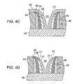
- FIGS. 4A-Gshow a cross sectional example of a preferred stylus tip cell formed according to the preferred method of FIG. 2A-B .
- the orifice 200has a circular horizontal cross section.
- Tip formation in step 108 of FIG. 2A as successive conformal layersare deposited in step 1080 and isotropically etched in step 1082 to form sidewall spacers 206 , 208 , forming a ring around the interior of the orifices 200 .
- a third 15 nm thick conformal layer 210is deposited completing the cross section in the example of FIG. 4A .
- a third spacer 212is formed in FIG. 4B , also forming a ring around the interior of the orifice 200 .
- a fourth 15 nm thick conformal layer 214is formed in step 1080 and isotropically etched in step 1082 to form fourth spacers 216 in FIG.
- spacer rings 206 , 208 , 212 and 216are shown as individual layers, this is primarily for illustration. If such spacers 206 , 208 , 212 and 216 are the same material, once formed, each would merge with previously formed spacer rings for a uniform, rather than layered, tip mold 218 .
- the spacerwould have the curvature of the deposited conformal film.
- heightis removed from each spacer 206 , 208 , 212 and 216 as it is slightly etched down with horizontal portion removal. Accordingly, the combined after etch thickness of the four spacers must be less than half the width of the orifice and may extend the full height of the orifice 200 to avoid plugging the orifice 200 .
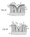
- Stylus tip cell formation in step 110 of FIG. 2Bbegins in step 1100 as shown in FIG. 4E as a phase change material layer 218 , preferably a conformal layer, is deposited in the orifice 200 .
- a conductive barrier layere.g., TiN, not shown
- the phase change material layer 218contacts the bottom electrode 204 , directly or indirectly, e.g., through a conductive barrier layer (not shown). Then, in step 1102 using RIE for example, the horizontal portions of phase change layer 218 are removed, leaving a phase change tip 222 in the orifice.
- the phase change tip 222 volumeis minimized with a cross section shaped similar to an arrowhead.
- the orificeis filled with conductive material 224 , plugging the mold and completing the stylus.
- conductive material 224is, preferably, TiN or TaN and, alternately, an n-type semiconductor.
- the phase change tip 222is sandwiched between the conductive material 224 (which may be formed with and act as a top electrode) and the bottom electrode 204 .
- the phase change tip 222in its crystalline phase, is an asymmetric resistor in the current path between the conductive material 224 and the bottom electrode 204 and favors electron conduction when the top electrode is biased negatively with respect to the bottom electrode.
- the phase change tip 222acts as an insulator, i.e., opening the current path.
- a one and a zerocan be represented by the absence and presence of asymmetric resistance (i.e., of crystalline phase change material) in the path or vice versa.
- the conductive material fill 224is planarized, e.g., CMP, leaving a conductive plug completing each stylus and top electrodes are formed.
- the conductive material fill 224may be patterned to integrally form the top electrodes with the conductive plugs.
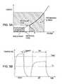
- FIG. 5Ashows an example of a current verses voltage (I-V) characteristic for a typical chalcogenide suitable as a phase change memory material for preferred embodiment cross point cells.
- FIG. 5Bshows an example of typical chalcogenide memory programming temperature evolution profiles for preferred embodiment cross point cells.
- Joule heatingis applied to the cell GST tip to switch phases: switching to its amorphous (RESET) phase by heating the GST to T melt and allowing it sufficient time to cool (t quench ); and, alternately, crystallizing (SET) the GST by heating it to T x and allowing it sufficient time to cool (t set ).
- REETamorphous
- SETcrystallizing
- amorphous GSTmay be a logic zero and crystalline GST may be a logic one.
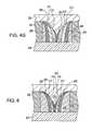
- FIG. 6shows a cross-section of another example of a preferred stylus 230 formed by depositing sequentially thinner layers such that spacers decrease in thickness axially, i.e., the initial spacer layer is much thicker than the final spacer layer.
- the first or outer layer 206 ′is substantially thicker than the inner layers 208 ′, 212 ′ and 216 ′.
- the outer layer 206 ′is from one quarter to one third the thickness of the horizontal dimension of the orifice.
- Subsequent spacer layersare each one quarter to one third as thick as the remaining opening at the bottom part of the spacer 208 ′. So, the effective thickness of each succeeding layer decreases geometrically the with the number of layers.
- a stylus tip and conductive materialare deposited to form the stylus 230 in the tapered mold.
- the phase change material layeris volume limited and concentrated in the stylus tip, bounded on all sides by the tip mold and on top by the conductor to the top electrode. So, the energy required to change phases is minimized because heat generated for setting/resetting the phase change material tip is, more or less, contained within the phase change material itself.
- the memory cellhas a more controlled resistance due to the limited for phase change material volume.
- the tip mold materialis a better heat insulator than conductor, which in combination with the conductive plug focuses the heat delivered to the cell on changing the phase, further improving device switching efficiency.
Landscapes
- Engineering & Computer Science (AREA)
- Manufacturing & Machinery (AREA)
- Semiconductor Memories (AREA)
Abstract
Description
Claims (18)
Priority Applications (3)
| Application Number | Priority Date | Filing Date | Title |
|---|---|---|---|
| US10/732,580US7928420B2 (en) | 2003-12-10 | 2003-12-10 | Phase change tip storage cell |
| CN200410094745.5ACN100524874C (en) | 2003-12-10 | 2004-11-17 | Phase change tip storage cell, integrated circuit and manufacturing method thereof |
| US12/136,158US7795068B2 (en) | 2003-12-10 | 2008-06-10 | Method of making integrated circuit (IC) including at least one storage cell |
Applications Claiming Priority (1)
| Application Number | Priority Date | Filing Date | Title |
|---|---|---|---|
| US10/732,580US7928420B2 (en) | 2003-12-10 | 2003-12-10 | Phase change tip storage cell |
Related Child Applications (1)
| Application Number | Title | Priority Date | Filing Date |
|---|---|---|---|
| US12/136,158DivisionUS7795068B2 (en) | 2003-12-10 | 2008-06-10 | Method of making integrated circuit (IC) including at least one storage cell |
Publications (2)
| Publication Number | Publication Date |
|---|---|
| US20050127349A1 US20050127349A1 (en) | 2005-06-16 |
| US7928420B2true US7928420B2 (en) | 2011-04-19 |
Family
ID=34652899
Family Applications (2)
| Application Number | Title | Priority Date | Filing Date |
|---|---|---|---|
| US10/732,580Expired - LifetimeUS7928420B2 (en) | 2003-12-10 | 2003-12-10 | Phase change tip storage cell |
| US12/136,158Expired - Fee RelatedUS7795068B2 (en) | 2003-12-10 | 2008-06-10 | Method of making integrated circuit (IC) including at least one storage cell |
Family Applications After (1)
| Application Number | Title | Priority Date | Filing Date |
|---|---|---|---|
| US12/136,158Expired - Fee RelatedUS7795068B2 (en) | 2003-12-10 | 2008-06-10 | Method of making integrated circuit (IC) including at least one storage cell |
Country Status (2)
| Country | Link |
|---|---|
| US (2) | US7928420B2 (en) |
| CN (1) | CN100524874C (en) |
Families Citing this family (90)
| Publication number | Priority date | Publication date | Assignee | Title |
|---|---|---|---|---|
| KR100598100B1 (en)* | 2004-03-19 | 2006-07-07 | 삼성전자주식회사 | Manufacturing method of phase change memory device |
| US20060034116A1 (en)* | 2004-08-13 | 2006-02-16 | Lam Chung H | Cross point array cell with series connected semiconductor diode and phase change storage media |
| US20070023857A1 (en)* | 2005-07-29 | 2007-02-01 | Ming Jin | Fabricating sub-lithographic contacts |
| US7786460B2 (en) | 2005-11-15 | 2010-08-31 | Macronix International Co., Ltd. | Phase change memory device and manufacturing method |
| US7635855B2 (en) | 2005-11-15 | 2009-12-22 | Macronix International Co., Ltd. | I-shaped phase change memory cell |
| US7449710B2 (en) | 2005-11-21 | 2008-11-11 | Macronix International Co., Ltd. | Vacuum jacket for phase change memory element |
| US7599217B2 (en) | 2005-11-22 | 2009-10-06 | Macronix International Co., Ltd. | Memory cell device and manufacturing method |
| US7459717B2 (en) | 2005-11-28 | 2008-12-02 | Macronix International Co., Ltd. | Phase change memory cell and manufacturing method |
| US7688619B2 (en)* | 2005-11-28 | 2010-03-30 | Macronix International Co., Ltd. | Phase change memory cell and manufacturing method |
| US7531825B2 (en) | 2005-12-27 | 2009-05-12 | Macronix International Co., Ltd. | Method for forming self-aligned thermal isolation cell for a variable resistance memory array |
| US8062833B2 (en) | 2005-12-30 | 2011-11-22 | Macronix International Co., Ltd. | Chalcogenide layer etching method |
| US7741636B2 (en) | 2006-01-09 | 2010-06-22 | Macronix International Co., Ltd. | Programmable resistive RAM and manufacturing method |
| US7560337B2 (en) | 2006-01-09 | 2009-07-14 | Macronix International Co., Ltd. | Programmable resistive RAM and manufacturing method |
| US7825396B2 (en)* | 2006-01-11 | 2010-11-02 | Macronix International Co., Ltd. | Self-align planerized bottom electrode phase change memory and manufacturing method |
| US7910907B2 (en)* | 2006-03-15 | 2011-03-22 | Macronix International Co., Ltd. | Manufacturing method for pipe-shaped electrode phase change memory |
| US7785920B2 (en) | 2006-07-12 | 2010-08-31 | Macronix International Co., Ltd. | Method for making a pillar-type phase change memory element |
| US8084799B2 (en)* | 2006-07-18 | 2011-12-27 | Qimonda Ag | Integrated circuit with memory having a step-like programming characteristic |
| US7688618B2 (en)* | 2006-07-18 | 2010-03-30 | Qimonda North America Corp. | Integrated circuit having memory having a step-like programming characteristic |
| US7772581B2 (en)* | 2006-09-11 | 2010-08-10 | Macronix International Co., Ltd. | Memory device having wide area phase change element and small electrode contact area |
| US7504653B2 (en) | 2006-10-04 | 2009-03-17 | Macronix International Co., Ltd. | Memory cell device with circumferentially-extending memory element |
| US7863655B2 (en) | 2006-10-24 | 2011-01-04 | Macronix International Co., Ltd. | Phase change memory cells with dual access devices |
| KR101275799B1 (en)* | 2006-11-21 | 2013-06-18 | 삼성전자주식회사 | Method of forming phase change layer using Ge precursor for low temperature deposition and method of manufacturing phase change memory device using the same |
| US7476587B2 (en) | 2006-12-06 | 2009-01-13 | Macronix International Co., Ltd. | Method for making a self-converged memory material element for memory cell |
| US7903447B2 (en) | 2006-12-13 | 2011-03-08 | Macronix International Co., Ltd. | Method, apparatus and computer program product for read before programming process on programmable resistive memory cell |
| US7718989B2 (en) | 2006-12-28 | 2010-05-18 | Macronix International Co., Ltd. | Resistor random access memory cell device |
| US7956344B2 (en) | 2007-02-27 | 2011-06-07 | Macronix International Co., Ltd. | Memory cell with memory element contacting ring-shaped upper end of bottom electrode |
| US7786461B2 (en) | 2007-04-03 | 2010-08-31 | Macronix International Co., Ltd. | Memory structure with reduced-size memory element between memory material portions |
| US7569844B2 (en)* | 2007-04-17 | 2009-08-04 | Macronix International Co., Ltd. | Memory cell sidewall contacting side electrode |
| US7729161B2 (en) | 2007-08-02 | 2010-06-01 | Macronix International Co., Ltd. | Phase change memory with dual word lines and source lines and method of operating same |
| US7919766B2 (en) | 2007-10-22 | 2011-04-05 | Macronix International Co., Ltd. | Method for making self aligning pillar memory cell device |
| US8084842B2 (en) | 2008-03-25 | 2011-12-27 | Macronix International Co., Ltd. | Thermally stabilized electrode structure |
| US8030634B2 (en)* | 2008-03-31 | 2011-10-04 | Macronix International Co., Ltd. | Memory array with diode driver and method for fabricating the same |
| US7825398B2 (en) | 2008-04-07 | 2010-11-02 | Macronix International Co., Ltd. | Memory cell having improved mechanical stability |
| US7791057B2 (en) | 2008-04-22 | 2010-09-07 | Macronix International Co., Ltd. | Memory cell having a buried phase change region and method for fabricating the same |
| KR20090116500A (en)* | 2008-05-07 | 2009-11-11 | 삼성전자주식회사 | Phase change memory device and forming method thereof |
| US8077505B2 (en) | 2008-05-07 | 2011-12-13 | Macronix International Co., Ltd. | Bipolar switching of phase change device |
| US7701750B2 (en) | 2008-05-08 | 2010-04-20 | Macronix International Co., Ltd. | Phase change device having two or more substantial amorphous regions in high resistance state |
| US8415651B2 (en) | 2008-06-12 | 2013-04-09 | Macronix International Co., Ltd. | Phase change memory cell having top and bottom sidewall contacts |
| US8134857B2 (en) | 2008-06-27 | 2012-03-13 | Macronix International Co., Ltd. | Methods for high speed reading operation of phase change memory and device employing same |
| US7932506B2 (en) | 2008-07-22 | 2011-04-26 | Macronix International Co., Ltd. | Fully self-aligned pore-type memory cell having diode access device |
| US7903457B2 (en) | 2008-08-19 | 2011-03-08 | Macronix International Co., Ltd. | Multiple phase change materials in an integrated circuit for system on a chip application |
| US7719913B2 (en) | 2008-09-12 | 2010-05-18 | Macronix International Co., Ltd. | Sensing circuit for PCRAM applications |
| US8324605B2 (en) | 2008-10-02 | 2012-12-04 | Macronix International Co., Ltd. | Dielectric mesh isolated phase change structure for phase change memory |
| US7897954B2 (en) | 2008-10-10 | 2011-03-01 | Macronix International Co., Ltd. | Dielectric-sandwiched pillar memory device |
| KR101486984B1 (en)* | 2008-10-30 | 2015-01-30 | 삼성전자주식회사 | Variable resistance memory device and method of forming the same |
| US8097870B2 (en)* | 2008-11-05 | 2012-01-17 | Seagate Technology Llc | Memory cell with alignment structure |
| US8036014B2 (en) | 2008-11-06 | 2011-10-11 | Macronix International Co., Ltd. | Phase change memory program method without over-reset |
| US7869270B2 (en) | 2008-12-29 | 2011-01-11 | Macronix International Co., Ltd. | Set algorithm for phase change memory cell |
| US8089137B2 (en) | 2009-01-07 | 2012-01-03 | Macronix International Co., Ltd. | Integrated circuit memory with single crystal silicon on silicide driver and manufacturing method |
| US8107283B2 (en) | 2009-01-12 | 2012-01-31 | Macronix International Co., Ltd. | Method for setting PCRAM devices |
| US8030635B2 (en) | 2009-01-13 | 2011-10-04 | Macronix International Co., Ltd. | Polysilicon plug bipolar transistor for phase change memory |
| US8064247B2 (en) | 2009-01-14 | 2011-11-22 | Macronix International Co., Ltd. | Rewritable memory device based on segregation/re-absorption |
| US8933536B2 (en)* | 2009-01-22 | 2015-01-13 | Macronix International Co., Ltd. | Polysilicon pillar bipolar transistor with self-aligned memory element |
| US8084760B2 (en)* | 2009-04-20 | 2011-12-27 | Macronix International Co., Ltd. | Ring-shaped electrode and manufacturing method for same |
| US8173987B2 (en) | 2009-04-27 | 2012-05-08 | Macronix International Co., Ltd. | Integrated circuit 3D phase change memory array and manufacturing method |
| US8097871B2 (en) | 2009-04-30 | 2012-01-17 | Macronix International Co., Ltd. | Low operational current phase change memory structures |
| US7933139B2 (en) | 2009-05-15 | 2011-04-26 | Macronix International Co., Ltd. | One-transistor, one-resistor, one-capacitor phase change memory |
| US8350316B2 (en)* | 2009-05-22 | 2013-01-08 | Macronix International Co., Ltd. | Phase change memory cells having vertical channel access transistor and memory plane |
| US7968876B2 (en) | 2009-05-22 | 2011-06-28 | Macronix International Co., Ltd. | Phase change memory cell having vertical channel access transistor |
| US8809829B2 (en) | 2009-06-15 | 2014-08-19 | Macronix International Co., Ltd. | Phase change memory having stabilized microstructure and manufacturing method |
| US8406033B2 (en) | 2009-06-22 | 2013-03-26 | Macronix International Co., Ltd. | Memory device and method for sensing and fixing margin cells |
| US8363463B2 (en) | 2009-06-25 | 2013-01-29 | Macronix International Co., Ltd. | Phase change memory having one or more non-constant doping profiles |
| US8238149B2 (en) | 2009-06-25 | 2012-08-07 | Macronix International Co., Ltd. | Methods and apparatus for reducing defect bits in phase change memory |
| US8110822B2 (en) | 2009-07-15 | 2012-02-07 | Macronix International Co., Ltd. | Thermal protect PCRAM structure and methods for making |
| US7894254B2 (en) | 2009-07-15 | 2011-02-22 | Macronix International Co., Ltd. | Refresh circuitry for phase change memory |
| US8198619B2 (en) | 2009-07-15 | 2012-06-12 | Macronix International Co., Ltd. | Phase change memory cell structure |
| US8064248B2 (en) | 2009-09-17 | 2011-11-22 | Macronix International Co., Ltd. | 2T2R-1T1R mix mode phase change memory array |
| US8159857B2 (en)* | 2009-09-21 | 2012-04-17 | Infineon Technologies Ag | Electronic device with a programmable resistive element and a method for blocking a device |
| US8178387B2 (en) | 2009-10-23 | 2012-05-15 | Macronix International Co., Ltd. | Methods for reducing recrystallization time for a phase change material |
| TWI449170B (en)* | 2009-12-29 | 2014-08-11 | Ind Tech Res Inst | Phase change memory devices and fabrication methods thereof |
| US8729521B2 (en) | 2010-05-12 | 2014-05-20 | Macronix International Co., Ltd. | Self aligned fin-type programmable memory cell |
| US8310864B2 (en) | 2010-06-15 | 2012-11-13 | Macronix International Co., Ltd. | Self-aligned bit line under word line memory array |
| US8395935B2 (en) | 2010-10-06 | 2013-03-12 | Macronix International Co., Ltd. | Cross-point self-aligned reduced cell size phase change memory |
| US8497705B2 (en) | 2010-11-09 | 2013-07-30 | Macronix International Co., Ltd. | Phase change device for interconnection of programmable logic device |
| US8467238B2 (en) | 2010-11-15 | 2013-06-18 | Macronix International Co., Ltd. | Dynamic pulse operation for phase change memory |
| CN102554783B (en) | 2010-12-23 | 2014-12-03 | 中芯国际集成电路制造(上海)有限公司 | Cleaning method of grinding pad |
| US8987700B2 (en) | 2011-12-02 | 2015-03-24 | Macronix International Co., Ltd. | Thermally confined electrode for programmable resistance memory |
| US9136473B2 (en)* | 2013-03-28 | 2015-09-15 | Stmicroelectronics, Inc. | Semiconductor device with PCM memory cells and nanotubes and related methods |
| US9112148B2 (en)* | 2013-09-30 | 2015-08-18 | Taiwan Semiconductor Manufacturing Co., Ltd. | RRAM cell structure with laterally offset BEVA/TEVA |
| US9336879B2 (en) | 2014-01-24 | 2016-05-10 | Macronix International Co., Ltd. | Multiple phase change materials in an integrated circuit for system on a chip application |
| US9178144B1 (en) | 2014-04-14 | 2015-11-03 | Taiwan Semiconductor Manufacturing Co., Ltd. | RRAM cell with bottom electrode |
| US9559113B2 (en) | 2014-05-01 | 2017-01-31 | Macronix International Co., Ltd. | SSL/GSL gate oxide in 3D vertical channel NAND |
| CN105098068A (en)* | 2014-05-22 | 2015-11-25 | 中芯国际集成电路制造(上海)有限公司 | Semiconductor device, manufacturing method thereof and electronic device |
| US9406522B2 (en) | 2014-07-24 | 2016-08-02 | Applied Materials, Inc. | Single platform, multiple cycle spacer deposition and etch |
| US9209392B1 (en) | 2014-10-14 | 2015-12-08 | Taiwan Semiconductor Manufacturing Co., Ltd. | RRAM cell with bottom electrode |
| JP2018500754A (en)* | 2014-11-26 | 2018-01-11 | マイクロチップ テクノロジー インコーポレイテッドMicrochip Technology Incorporated | Resistive memory cell with spacer region for reduced conductive path area / increased electric field |
| US9672906B2 (en) | 2015-06-19 | 2017-06-06 | Macronix International Co., Ltd. | Phase change memory with inter-granular switching |
| US11050023B2 (en)* | 2019-07-01 | 2021-06-29 | International Business Machines Corporation | CBRAM with controlled bridge location |
| US20210202839A1 (en)* | 2018-07-10 | 2021-07-01 | National Institute Of Advanced Industrial Science And Technology | Stacked structure and method of manufacturing same, and semiconductor device |
| US20230397511A1 (en)* | 2022-06-01 | 2023-12-07 | Taiwan Semiconductor Manufacturing Company Limited | Planarization-less phase change material switch |
Citations (5)
| Publication number | Priority date | Publication date | Assignee | Title |
|---|---|---|---|---|
| US5920788A (en)* | 1995-06-07 | 1999-07-06 | Micron Technology, Inc. | Chalcogenide memory cell with a plurality of chalcogenide electrodes |
| US6507061B1 (en)* | 2001-08-31 | 2003-01-14 | Intel Corporation | Multiple layer phase-change memory |
| US6586761B2 (en) | 2001-09-07 | 2003-07-01 | Intel Corporation | Phase change material memory device |
| US6937507B2 (en)* | 2003-12-05 | 2005-08-30 | Silicon Storage Technology, Inc. | Memory device and method of operating same |
| US7012273B2 (en)* | 2003-08-14 | 2006-03-14 | Silicon Storage Technology, Inc. | Phase change memory device employing thermal-electrical contacts with narrowing electrical current paths |
Family Cites Families (2)
| Publication number | Priority date | Publication date | Assignee | Title |
|---|---|---|---|---|
| US6074516A (en)* | 1998-06-23 | 2000-06-13 | Lam Research Corporation | High sputter, etch resistant window for plasma processing chambers |
| US6849868B2 (en)* | 2002-03-14 | 2005-02-01 | Micron Technology, Inc. | Methods and apparatus for resistance variable material cells |
- 2003
- 2003-12-10USUS10/732,580patent/US7928420B2/ennot_activeExpired - Lifetime
- 2004
- 2004-11-17CNCN200410094745.5Apatent/CN100524874C/ennot_activeExpired - Fee Related
- 2008
- 2008-06-10USUS12/136,158patent/US7795068B2/ennot_activeExpired - Fee Related
Patent Citations (6)
| Publication number | Priority date | Publication date | Assignee | Title |
|---|---|---|---|---|
| US5920788A (en)* | 1995-06-07 | 1999-07-06 | Micron Technology, Inc. | Chalcogenide memory cell with a plurality of chalcogenide electrodes |
| US6507061B1 (en)* | 2001-08-31 | 2003-01-14 | Intel Corporation | Multiple layer phase-change memory |
| US6586761B2 (en) | 2001-09-07 | 2003-07-01 | Intel Corporation | Phase change material memory device |
| US6908812B2 (en)* | 2001-09-07 | 2005-06-21 | Intel Corporation | Phase change material memory device |
| US7012273B2 (en)* | 2003-08-14 | 2006-03-14 | Silicon Storage Technology, Inc. | Phase change memory device employing thermal-electrical contacts with narrowing electrical current paths |
| US6937507B2 (en)* | 2003-12-05 | 2005-08-30 | Silicon Storage Technology, Inc. | Memory device and method of operating same |
Also Published As
| Publication number | Publication date |
|---|---|
| CN100524874C (en) | 2009-08-05 |
| CN1627547A (en) | 2005-06-15 |
| US20080248624A1 (en) | 2008-10-09 |
| US7795068B2 (en) | 2010-09-14 |
| US20050127349A1 (en) | 2005-06-16 |
Similar Documents
| Publication | Publication Date | Title |
|---|---|---|
| US7928420B2 (en) | Phase change tip storage cell | |
| US7928012B2 (en) | Integrated circuit with upstanding stylus | |
| US7057923B2 (en) | Field emission phase change diode memory | |
| US7825398B2 (en) | Memory cell having improved mechanical stability | |
| CN101461071B (en) | A vertical phase change memory cell and methods for manufacturing thereof | |
| US7923285B2 (en) | Method for forming self-aligned thermal isolation cell for a variable resistance memory array | |
| US7772581B2 (en) | Memory device having wide area phase change element and small electrode contact area | |
| US7791057B2 (en) | Memory cell having a buried phase change region and method for fabricating the same | |
| US7521281B2 (en) | Methods of forming phase-changeable memory devices | |
| CN102522374B (en) | A phase-change memory device with a columnar bottom electrode and its manufacturing method | |
| US8415651B2 (en) | Phase change memory cell having top and bottom sidewall contacts | |
| CN100593865C (en) | Structure and method for improving thermal insulation of active sidewall phase change memory cell | |
| KR100880667B1 (en) | Memory cells with sidewall spacers for improved homogeneity | |
| CN101877384B (en) | Low Operating Current Phase Change Memory Element Structure | |
| US20090023242A1 (en) | Vacuum jacket for phase change memory element | |
| CN101013737A (en) | Thermal insulation phase change memory element and manufacturing method thereof | |
| US20080023685A1 (en) | Memory device and method of making same | |
| CN101237026A (en) | Memory cell with side electrode | |
| US8759808B2 (en) | Phase-change memory cell | |
| US20090045386A1 (en) | Phase-change memory element | |
| US7755074B2 (en) | Low area contact phase-change memory | |
| CN107274927B (en) | Phase change memory element and its application |
Legal Events
| Date | Code | Title | Description |
|---|---|---|---|
| AS | Assignment | Owner name:INTERNATIONAL BUSINESS MACHINES CORPORATION, NEW Y Free format text:ASSIGNMENT OF ASSIGNORS INTEREST;ASSIGNORS:HORAK, DAVID V.;WONG, PHILIP HON-SUM;LAM, CHUNG H.;REEL/FRAME:014470/0032;SIGNING DATES FROM 20040225 TO 20040326 Owner name:INTERNATIONAL BUSINESS MACHINES CORPORATION, NEW Y Free format text:ASSIGNMENT OF ASSIGNORS INTEREST;ASSIGNORS:HORAK, DAVID V.;WONG, PHILIP HON-SUM;LAM, CHUNG H.;SIGNING DATES FROM 20040225 TO 20040326;REEL/FRAME:014470/0032 | |
| STCF | Information on status: patent grant | Free format text:PATENTED CASE | |
| FPAY | Fee payment | Year of fee payment:4 | |
| AS | Assignment | Owner name:GLOBALFOUNDRIES U.S. 2 LLC, NEW YORK Free format text:ASSIGNMENT OF ASSIGNORS INTEREST;ASSIGNOR:INTERNATIONAL BUSINESS MACHINES CORPORATION;REEL/FRAME:036550/0001 Effective date:20150629 | |
| AS | Assignment | Owner name:GLOBALFOUNDRIES INC., CAYMAN ISLANDS Free format text:ASSIGNMENT OF ASSIGNORS INTEREST;ASSIGNORS:GLOBALFOUNDRIES U.S. 2 LLC;GLOBALFOUNDRIES U.S. INC.;REEL/FRAME:036779/0001 Effective date:20150910 | |
| MAFP | Maintenance fee payment | Free format text:PAYMENT OF MAINTENANCE FEE, 8TH YEAR, LARGE ENTITY (ORIGINAL EVENT CODE: M1552); ENTITY STATUS OF PATENT OWNER: LARGE ENTITY Year of fee payment:8 | |
| AS | Assignment | Owner name:WILMINGTON TRUST, NATIONAL ASSOCIATION, DELAWARE Free format text:SECURITY AGREEMENT;ASSIGNOR:GLOBALFOUNDRIES INC.;REEL/FRAME:049490/0001 Effective date:20181127 | |
| AS | Assignment | Owner name:GLOBALFOUNDRIES U.S. INC., CALIFORNIA Free format text:ASSIGNMENT OF ASSIGNORS INTEREST;ASSIGNOR:GLOBALFOUNDRIES INC.;REEL/FRAME:054633/0001 Effective date:20201022 | |
| AS | Assignment | Owner name:GLOBALFOUNDRIES INC., CAYMAN ISLANDS Free format text:RELEASE BY SECURED PARTY;ASSIGNOR:WILMINGTON TRUST, NATIONAL ASSOCIATION;REEL/FRAME:054636/0001 Effective date:20201117 | |
| AS | Assignment | Owner name:GLOBALFOUNDRIES U.S. INC., NEW YORK Free format text:RELEASE BY SECURED PARTY;ASSIGNOR:WILMINGTON TRUST, NATIONAL ASSOCIATION;REEL/FRAME:056987/0001 Effective date:20201117 | |
| MAFP | Maintenance fee payment | Free format text:PAYMENT OF MAINTENANCE FEE, 12TH YEAR, LARGE ENTITY (ORIGINAL EVENT CODE: M1553); ENTITY STATUS OF PATENT OWNER: LARGE ENTITY Year of fee payment:12 |