US7928015B2 - Solar cell fabrication using extruded dopant-bearing materials - Google Patents
Solar cell fabrication using extruded dopant-bearing materialsDownload PDFInfo
- Publication number
- US7928015B2 US7928015B2US11/609,825US60982506AUS7928015B2US 7928015 B2US7928015 B2US 7928015B2US 60982506 AUS60982506 AUS 60982506AUS 7928015 B2US7928015 B2US 7928015B2
- Authority
- US
- United States
- Prior art keywords
- dopant
- semiconductor substrate
- extruded
- ink
- surface area
- Prior art date
- Legal status (The legal status is an assumption and is not a legal conclusion. Google has not performed a legal analysis and makes no representation as to the accuracy of the status listed.)
- Expired - Fee Related, expires
Links
Images


Classifications
- H—ELECTRICITY
- H10—SEMICONDUCTOR DEVICES; ELECTRIC SOLID-STATE DEVICES NOT OTHERWISE PROVIDED FOR
- H10F—INORGANIC SEMICONDUCTOR DEVICES SENSITIVE TO INFRARED RADIATION, LIGHT, ELECTROMAGNETIC RADIATION OF SHORTER WAVELENGTH OR CORPUSCULAR RADIATION
- H10F10/00—Individual photovoltaic cells, e.g. solar cells
- H—ELECTRICITY
- H01—ELECTRIC ELEMENTS
- H01L—SEMICONDUCTOR DEVICES NOT COVERED BY CLASS H10
- H01L21/00—Processes or apparatus adapted for the manufacture or treatment of semiconductor or solid state devices or of parts thereof
- H01L21/02—Manufacture or treatment of semiconductor devices or of parts thereof
- H01L21/04—Manufacture or treatment of semiconductor devices or of parts thereof the devices having potential barriers, e.g. a PN junction, depletion layer or carrier concentration layer
- H01L21/18—Manufacture or treatment of semiconductor devices or of parts thereof the devices having potential barriers, e.g. a PN junction, depletion layer or carrier concentration layer the devices having semiconductor bodies comprising elements of Group IV of the Periodic Table or AIIIBV compounds with or without impurities, e.g. doping materials
- H01L21/22—Diffusion of impurity materials, e.g. doping materials, electrode materials, into or out of a semiconductor body, or between semiconductor regions; Interactions between two or more impurities; Redistribution of impurities
- H01L21/225—Diffusion of impurity materials, e.g. doping materials, electrode materials, into or out of a semiconductor body, or between semiconductor regions; Interactions between two or more impurities; Redistribution of impurities using diffusion into or out of a solid from or into a solid phase, e.g. a doped oxide layer
- H01L21/2251—Diffusion into or out of group IV semiconductors
- H01L21/2254—Diffusion into or out of group IV semiconductors from or through or into an applied layer, e.g. photoresist, nitrides
- H—ELECTRICITY
- H01—ELECTRIC ELEMENTS
- H01L—SEMICONDUCTOR DEVICES NOT COVERED BY CLASS H10
- H01L21/00—Processes or apparatus adapted for the manufacture or treatment of semiconductor or solid state devices or of parts thereof
- H01L21/02—Manufacture or treatment of semiconductor devices or of parts thereof
- H01L21/04—Manufacture or treatment of semiconductor devices or of parts thereof the devices having potential barriers, e.g. a PN junction, depletion layer or carrier concentration layer
- H01L21/18—Manufacture or treatment of semiconductor devices or of parts thereof the devices having potential barriers, e.g. a PN junction, depletion layer or carrier concentration layer the devices having semiconductor bodies comprising elements of Group IV of the Periodic Table or AIIIBV compounds with or without impurities, e.g. doping materials
- H01L21/22—Diffusion of impurity materials, e.g. doping materials, electrode materials, into or out of a semiconductor body, or between semiconductor regions; Interactions between two or more impurities; Redistribution of impurities
- H01L21/228—Diffusion of impurity materials, e.g. doping materials, electrode materials, into or out of a semiconductor body, or between semiconductor regions; Interactions between two or more impurities; Redistribution of impurities using diffusion into or out of a solid from or into a liquid phase, e.g. alloy diffusion processes
- H—ELECTRICITY
- H10—SEMICONDUCTOR DEVICES; ELECTRIC SOLID-STATE DEVICES NOT OTHERWISE PROVIDED FOR
- H10F—INORGANIC SEMICONDUCTOR DEVICES SENSITIVE TO INFRARED RADIATION, LIGHT, ELECTROMAGNETIC RADIATION OF SHORTER WAVELENGTH OR CORPUSCULAR RADIATION
- H10F10/00—Individual photovoltaic cells, e.g. solar cells
- H10F10/10—Individual photovoltaic cells, e.g. solar cells having potential barriers
- H10F10/14—Photovoltaic cells having only PN homojunction potential barriers
- H10F10/146—Back-junction photovoltaic cells, e.g. having interdigitated base-emitter regions on the back side
- H—ELECTRICITY
- H10—SEMICONDUCTOR DEVICES; ELECTRIC SOLID-STATE DEVICES NOT OTHERWISE PROVIDED FOR
- H10F—INORGANIC SEMICONDUCTOR DEVICES SENSITIVE TO INFRARED RADIATION, LIGHT, ELECTROMAGNETIC RADIATION OF SHORTER WAVELENGTH OR CORPUSCULAR RADIATION
- H10F71/00—Manufacture or treatment of devices covered by this subclass
- H10F71/137—Batch treatment of the devices
- H10F71/1375—Apparatus for automatic interconnection of photovoltaic cells in a module
- H—ELECTRICITY
- H10—SEMICONDUCTOR DEVICES; ELECTRIC SOLID-STATE DEVICES NOT OTHERWISE PROVIDED FOR
- H10F—INORGANIC SEMICONDUCTOR DEVICES SENSITIVE TO INFRARED RADIATION, LIGHT, ELECTROMAGNETIC RADIATION OF SHORTER WAVELENGTH OR CORPUSCULAR RADIATION
- H10F77/00—Constructional details of devices covered by this subclass
- H10F77/20—Electrodes
- H10F77/206—Electrodes for devices having potential barriers
- H10F77/211—Electrodes for devices having potential barriers for photovoltaic cells
- Y—GENERAL TAGGING OF NEW TECHNOLOGICAL DEVELOPMENTS; GENERAL TAGGING OF CROSS-SECTIONAL TECHNOLOGIES SPANNING OVER SEVERAL SECTIONS OF THE IPC; TECHNICAL SUBJECTS COVERED BY FORMER USPC CROSS-REFERENCE ART COLLECTIONS [XRACs] AND DIGESTS
- Y02—TECHNOLOGIES OR APPLICATIONS FOR MITIGATION OR ADAPTATION AGAINST CLIMATE CHANGE
- Y02E—REDUCTION OF GREENHOUSE GAS [GHG] EMISSIONS, RELATED TO ENERGY GENERATION, TRANSMISSION OR DISTRIBUTION
- Y02E10/00—Energy generation through renewable energy sources
- Y02E10/50—Photovoltaic [PV] energy
- Y02E10/547—Monocrystalline silicon PV cells
Definitions
- This inventionrelates to the production of semiconductor devices, and in particular to the low cost production of large-area devices, such as silicon wafer-based solar cells, and power semiconductor devices by utilizing extrusion methods to form doped regions in the semiconductor substrate of the semiconductor device.
- Modern solar cellstypically include a large-area, single layer p-n junction diode that is capable of generating electrical energy from solar light. These cells are typically made using silicon wafers that are doped to include one or more n-type doped regions, and one or more p-type doped regions. Such solar cells (also known as silicon wafer-based solar cells) are currently the dominant technology in the commercial production of solar cells, and are the main focus of the present invention.
- a desirable solar cell geometrycommonly referred to as the interdigitated back contact (IBC) cell, consists of a semiconductor wafer, such as silicon, and alternating lines (interdigitated stripes) of p-type and n-type doping.
- This cell architecturehas the advantage that all of the electrical contacts to the p and n regions can be made to one side of the wafer. When the wafers are connected together into a module, the wiring is all done from one side.
- Device structure and fabrication means for this devicehave been described previously in co-owned and co-pending U.S. patent application Ser. No. 11/336,714 entitled “Solar Cell Production Using Non-Contact Patterning and Direct-Write Metallization”, which is incorporated herein by reference in its entirety.
- One method for forming the alternately doped line regions in an IBC solar cellis to dispose dopant bearing pastes of alternating dopant type on the wafer, and then to heat the wafer with the appropriate temperature profile to drive in the dopants.
- Solar cell doping and the patterning of doped regionsis typically carried out with costly steps that may include the use of barrier deposition, barrier patterning, laser processing, damage removal, and gas phase furnace diffusion.
- screen printing techniquesa distinct disadvantage of screen printing is that two separate print operations would be needed to write the two dopant bearing materials, and the two prints would need to beakily well registered.
- screen printingrequires contact with the wafer, which increases the risk of wafer damage (breakage), thus increasing overall production costs.
- the first screen printed layerneeds to be dried before a second screen print step is applied.
- One commonly used solar cell architectureutilizes the back surface of the cell wafer as a broad area metal pad, typically aluminum, to form a contact to the p-type side of the device.
- the aluminuminteracts with the silicon to form a p+ doped layer.
- the back surfaceis also doped with boron to produce a p+ layer.
- the role of this layeris to create a so-called back surface field which reduces the recombination of the photocurrent on the back metallization.
- the broad area metal layeris commonly applied either by screen printing or pad printing, both of which are contact printing methods, and therefore increase the risk of wafer breakage.
- What is neededis a low cost method and system for producing doped regions in solar cell substrates that avoids the problems associated with contact printing methods.
- what is neededis a simpler and more reliable method for producing self-registered p-type and n-type doped regions in the production of IBC solar cells.
- the present inventionis directed to a low cost method and system for producing large-area semiconductors that includes extruding a dopant bearing material (dopant ink) onto one or more predetermined surface areas of a semiconductor substrate (e.g., a monocrystalline silicon wafer), and then heating (thermal processing) the semiconductor substrate such that the dopant disposed in the dopant ink diffuses into the substrate to form the desired doped region or regions.
- a dopant bearing materialdopant ink
- a semiconductor substratee.g., a monocrystalline silicon wafer
- thermal processingthermal processing
- the extrusion of dopant material on the substrateprovides superior control of the feature resolution of the doped regions.
- the dopant inkcan be reliably disposed over the desired substrate regions without contacting the substrate, thereby avoiding the wafer breakage problem associated with conventional contact printing methods.
- the present inventionreduces the overall manufacturing costs associated with the production of large area semiconductor devices when compared with conventional production methods.
- a system for producing large area semiconductor devicesincludes forming desired doped regions in surface of a semiconductor substrate using the extrusion method described above, forming a passivation layer over the substrate surface, utilizing a laser ablation or other non-contact apparatus to form contact openings in the passivation layer, and then utilizing a direct-write metallization apparatus to deposit contact structures in the contact openings and to form metallization lines on the passivation layer.
- the present inventionfacilitates the reliable production of solar cells with minimal wafer breakage.
- residual dopant inkmay be removed from the substrate surface before forming the passivation layer.
- a system for production of IBC-type solar cellsincludes an extrusion head that is capable of simultaneously extruding interdigitated dopant ink structures having two different dopant types (e.g., n-type dopant ink and p-type dopant ink) in a self-registered arrangement on a substrate surface.
- the extrusion headincludes multiple nozzles (outlet channels) that respectively communicate at their inlet opening to a selected dopant ink source, and that have respective outlet openings disposed in a self-registered arrangement over the substrate surface.
- every other nozzlecommunicates with a p-type dopant ink source, and the remaining nozzles communicate with an n-type dopant ink source, whereby each p-type extruded structure is disposed between two n-type extruded structures.
- the systemincludes an x-y table or other mechanism for moving the substrate relative to the extrusion head during the extrusion process.
- the extrusion headis fabricated by laminating multiple sheets of micro-machined silicon, plastic or other non-ferrous materials. It is important to dispense the dopant ink without the introduction of harmful impurities, and transition metal impurities are in particular to be avoided. This requirement makes the use of ferrous metal-based fluidic systems undesirable.
- the bonding of micromachined silicon wafersis a well understood and reliable process.
- the extrusion headcan be formed such that the two dopant inks are fed from opposite sides of the nozzle array, or the extrusion head can be formed using a “side shooter” arrangement in which both dopant inks are fed from the same side to the nozzle array.
- a third (e.g., relatively light doping or non-doping) inkis extruded together with the two relatively heavy dopant inks such that each adjacent pair of heavy dopant ink structures is separated by a lightly or non-doping ink structure.
- the non-doping inkmay serve as a spacer between dopant ink structures and/or as barrier to prevent doping from the ambient.
- the heavily n-type and p-type doped structuresare separated by lightly doped ink that generates a lightly doped semiconductor region between the two heavily doped regions.
- the narrow lines of heavily doped inkare embedded between wider lines of a second (e.g., non-doping) ink.
- the narrow linesare generated by forming the extrusion head such that selected nozzle channels converge adjacent to their associated outlet openings.
- the nozzle channels for the non-doping inkdiverge prior to reaching the head outlet, which further squeezes the narrow lines and forms a continuous sheet in which the narrow lines are disposed between wide non-doping structures.
- Full control of the line widthis both a function of the extrusion head design as well as the relative flow rates of the materials.
- an extrusion headincludes a single plenum that feeds several diverging nozzle channels that terminate before an end facet of the extrusion head, thereby generating a flow merging section that produces a uniform extruded sheet of dopant or metal paste.
- This extrusion headprovides an alternative non-contact method for forming so-called back surface fields that reduce the recombination of the photocurrent on the back metallization, thereby reducing manufacturing costs by avoiding the wafer breakage associated with conventional screen printing or pad printing methods.
- a hybrid doping methoduses a combination of solid source doping and gas phase doping.
- Dopant ink structuresare extruded on a wafer in the manner described above, but non-doping structures are also formed on each side of the dopant ink structures, and gaps are intentionally formed such that selected surface areas are intentionally exposed between the extruded structures.
- a temperature anneal of the substrateis then performed in an ambient containing a gaseous phase dopant. The thermal processing in conjunction with the doping ambient results in both solid source doping in the covered regions, and ambient source doping in the exposed regions.
- extruded dopant ink structuresare capped (entirely covered) by a co-extruded material.
- a known problem with the solid source dopingis that while the dopants are diffusing, they diffuse out of the source and onto other parts of the wafer, creating an undesirable doping effect in the surrounding portions of the wafer.
- the capping structureis optionally removed after thermal treatment is completed.
- FIG. 1is a simplified perspective view showing a wafer processing apparatus in accordance with a generalized embodiment of the present invention
- FIG. 2is a block diagram showing a system for producing wafer-based solar cells using the wafer processing apparatus of FIG. 1 according to an embodiment of the present invention
- FIG. 3is a simplified perspective view showing a multiple dopant ink extrusion apparatus of a wafer processing apparatus according to another embodiment of the present invention.
- FIGS. 4(A) and 4(B)exploded and assembled perspective views, respectively, showing a portion of a multiple dopant ink extrusion head according to a specific embodiment of the present invention
- FIGS. 5(A) , 5 (B), 5 (C), 5 (D), 5 (E), 5 (F) and 5 (G)are perspective views illustrating various process stages during the fabrication of an IBC solar cell device using the system of FIG. 2 and extrusion head of FIG. 4(B) according to another embodiment of the present invention
- FIG. 6is an exploded perspective view showing a portion of a multiple dopant ink extrusion head according to another exemplary embodiment of the present invention.
- FIG. 7is a simplified perspective view showing a poly-extrusion head according to another exemplary embodiment of the present invention.
- FIG. 9is a simplified cross-sectional top view showing a poly-extrusion head according to another exemplary embodiment of the present invention.
- FIG. 10is a simplified cross-sectional top view showing a portion of an extrusion head for generating a wide sheet of dopant ink according to another exemplary embodiment of the present invention.
- FIG. 11is a simplified perspective view illustrating a hybrid doping method according to another embodiment of the present invention.
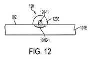
- FIG. 12is a simplified cross-sectional side view showing a capped dopant ink structure according to yet another embodiment of the present invention.
- FIG. 1is a simplified perspective view illustrating a wafer processing apparatus 100 for producing an integrated circuit (e.g., a solar cell) on a semiconductor substrate 101 in accordance with a generalized embodiment of the present invention.
- Wafer processing apparatus 100generally includes an extrusion apparatus 110 A for forming extruded structures 120 - 1 to 120 - 4 on substrate 101 during a first time period (Ti), and thermal processing (heating) apparatus 140 for heating substrate 101 during a second time period (T 2 ) such that dopant diffuses from extruded structures 120 - 1 to 120 - 4 into substrate 101 to form doped regions 101 - 1 to 101 - 4 , respectively. Subsequent processing of substrate 101 is described below.
- Extrusion apparatus 110 Aincludes an extrusion head (die) 130 that is operably coupled to a reservoir (dopant ink source) 111 containing a dopant ink 112 .
- Extrusionhas been utilized in a wide variety of applications, but is not believed to have been used in the production of large area semiconductor devices, and in particular in the formation of doped regions in a semiconductor substrate. Extrusion is a well-established manufacturing process that is typically used to create relatively long, narrow objects of a fixed cross-sectional profile.
- dopant ink 112is pushed and/or drawn through outlet orifices 135 - 1 to 135 - 4 , which are defined in extrusion head 130 using known techniques (e.g., using a suitable pump or auger), thereby generating multiple dopant ink beads 112 - 1 to 112 - 4 .
- Outlet orifices 135 - 1 to 135 - 4are formed in a selected shape (e.g., rectangular) such that beads 112 - 1 to 112 - 4 have the desired cross-sectional shape.
- extruded structures 120 - 1 to 120 - 4are separated by open (uncovered) regions of surface 102 .
- extruded structures 120 - 1 and 120 - 2are separated by an open surface region 102 - 31 .
- dopant ink 112includes a paste-like vehicle material into which a desired n-type or p-type dopant is disbursed.
- a suitable extrudable phosphorus dopant inkincludes one or more of a variety of organometallic phosphorus compounds in which phosphorus containing substituent groups are present in compounds with carbon chains of varying lengths. These compounds must either be liquids at room temperature or completely soluble in the other solvents present in the formulation.
- the phosphorus dopant inkalso includes dilute solutions of phosphoric acid.
- a fugitive organic vehicleis used that burns off or evaporates during processing. These vehicles are typically solutions of ethyl cellulose in high boiling solvents (b.p.
- the phosphorus dopant inkmay include Theological additives such as hydrogenated castor oil and plasticizers such as various phthalates (dimethyl phthalate, dibutyl phthalate, dioctyl phthalate, etc). Surfactants and wetting agents may be included as well.
- thermal processing apparatus 140is an oven or kiln maintained at a temperature of 850° C. or higher. This heating process causes the dopant disposed in extruded structures 120 - 1 to 120 - 4 to diffuse into substrate 101 through surface areas 102 - 1 to 102 - 4 , respectively, and to form doped regions 101 - 1 to 101 - 4 , respectively.
- extruded structures 120 - 1 to 120 - 4are separated by a sufficient distance such that each doped region is separated from adjacent doped regions by a region of lightly doped or intrinsic (undoped) silicon.
- doped regions 101 - 1 and 101 - 2are separated by an intrinsic region 101 - 31
- doped regions 101 - 2 and 101 - 3are separated by an intrinsic region 101 - 32
- doped regions 101 - 3 and 101 - 4are separated by an intrinsic region 101 - 33 .
- FIG. 2depicts a system 200 for fabricating wafer-based solar cells using extrusion-based wafer processing apparatus 100 ( FIG. 1 ) and other non-contact processing techniques in accordance with another embodiment of the present invention.
- the combined structure including substrate 101 and passivation layer 215is generally as “wafer” or “device 201”, and at each stage of the processing cycle is referenced with an appended suffix indicating the device's current processing stage (e.g., after formation of passivation layer 215 and prior to the ablation process described below, device 201 is referenced as “device 201T1”, with the suffix “T1” indicating a relatively early point in the process cycle).
- Device 201 T 1is then subjected to various non-contact processes in order to produce a usable solar cell.
- a laser ablation apparatus 230is utilized to define contact holes 217 through passivation layer 215 that expose corresponding portions of upper surface 102 of substrate 101 such that the contact holes are arranged in straight parallel rows over the doped diffusion regions.
- a suitable ablation processis described in additional detail in co-owned and co-pending U.S. patent application Ser. No. 11/562,383, filed Nov. 21, 2006, entitled “MULTIPLE STATION SCAN DISPLACEMENT INVARIANT LASER ABLATION APPARATUS”, which is incorporated herein by reference in its entirety.
- partially processed wafers 201 T 2are passed to a direct-write metallization apparatus 250 that is utilized to deposit contact structures 218 into contact holes 217 , and to form metal interconnect lines 219 on passivation layer 215 such that each metal interconnect line 219 connects the contact structures 218 disposed over an associated doped diffusion region. Additional details and alternative embodiments related to direct-write metallization device 250 are disclosed in co-owned U.S. patent application Ser. No. 11/336,714, cited above. Finally, metallized device 201 T 3 is passed from direct-write metallization apparatus 250 to an optional post-metallization processing apparatus 270 for subsequent processing to form the completed solar cell 201 T 4 .
- FIG. 3is a simplified illustration showing the extrusion portion of a wafer processing apparatus 100 B according to another embodiment of the present invention.
- Wafer processing apparatus 100 Bincludes an extrusion apparatus 110 B that supports an extrusion head 130 B over a substrate 101 B during the extrusion process.
- Wafer processing apparatus 100 Bdiffers from wafer processing apparatus 100 (described above) in that extrusion head 130 B communicates with two dopant bearing material sources 111 and 114 containing two different dopant inks 112 and 115 , and is capable of extruding dopant inks 112 and 115 such that they form extruded structures (lines) 120 in interdigitated arrangement onto semiconductor substrate 101 B.
- extrusion head 130 Bis formed such that dopant ink 112 is passed to a first set of outlet orifices 135 (e.g., outlet orifices 135 - 11 and 135 - 12 ), and dopant ink 115 is passed to a second, different set of outlet orifices 135 (e.g., orifice 135 - 21 and 135 - 22 ), where the first and second sets are alternately positioned along extrusion head 130 B.
- a first set of outlet orifices 135e.g., outlet orifices 135 - 11 and 135 - 12
- dopant ink 115is passed to a second, different set of outlet orifices 135 (e.g., orifice 135 - 21 and 135 - 22 )
- the first and second setsare alternately positioned along extrusion head 130 B.
- dopant ink 112is deposited as extruded structures 120 - 11 and 120 - 12 and dopant ink 115 is deposited as extruded structures 120 - 21 and 120 - 22 in an interdigitated arrangement (i.e., such that extruded structure 120 - 21 is disposed between extruded structures 120 - 11 and 120 - 12 ).
- extrusion apparatus 110 Boperates similar to an inkjet printing apparatus to provide for the translation of substrate 101 B-T 1 with respect to the extrusion head 130 B (i.e., either by moving extrusion head 130 B in the direction Y 1 over stationary substrate 101 B, or by moving substrate 101 B in the direction Y 2 under stationary extrusion head 130 B).
- Dopant inks 112 and 115are fed into extrusion head 130 B under pressure. Both applied fluid pressure and relative head-wafer motion are controlled by an automated system to produce lines 120 of controlled dimensions.
- a pitch of the interdigitated dopant ink lines 120is controlled by the spacing between adjacent outlet orifices 135 that is designed into extrusion head 130 B.
- an exposed surface area 102 - 31which is disposed between a first surface region 102 - 11 covered by extruded structure 120 - 11 and a second surface region 102 - 21 covered by extruded structure 120 - 21 , has a width that is determined by a spacing between adjacent edges of outlet orifices 135 - 11 and 135 - 21 .
- extrusion head 130 Bcan be fabricated with precision machining methods, such as lithographic etching and wafer bonding, very high precision, on the order of microns, is achievable for the spacing between adjacent extruded structures 120 . This novel approach to writing registered lines of dissimilar dopant inks exceeds all state of the art screen print methods.
- FIGS. 4(A) and 4(B)are exploded and assembled perspective views showing a portion of an extrusion head 130 B- 1 according to a specific embodiment of the present invention.
- Extrusion head 130 B- 1includes a central sheet 310 , upper and lower feedline sheets 320 and 330 , and upper and lower capping sheets 340 and 350 .
- Central sheet 310is micromachined to include multiple parallel nozzle channels (e.g., nozzle channels 315 - 11 , 315 - 12 , 315 - 21 and 315 - 22 ), where each nozzle channel has a closed end and an opposing open end defined in side edge 317 .
- feedline sheets 320 and 330are micromachined to include manifolds (plenums) and feed channels that are arranged to transfer dopant ink to corresponding nozzles of central sheet 310 .
- feedline sheet 320includes a plenum 322 that extends in a direction perpendicular to the nozzle channels, and includes feed channels 325 - 11 and 325 - 12 that communicate with plenum 322 and extend over the closed ends of nozzle channels 315 - 11 and 315 - 12 , respectively.
- feedline sheet 330includes a plenum 332 and feed channels 335 - 21 and 335 - 22 that extend over the closed ends of nozzle channels 315 - 21 and 315 - 12 , respectively.
- extrusion head 130 B- 1is produced using materials that do not introduce unwanted impurities, particularly impurities that would induce carrier recombination.
- Materialssuch as polytetrafluoroethylene (PTFE) and other chemically inert polymer materials or glass or silicon are preferred materials for constructing the extrusion head. It is important to dispense dopant ink 112 and 115 without the introduction of harmful impurities. Transition metal and other metal impurities are in particular to be avoided. These include gold, copper, iron etc. This makes the use of ferrous metal-based fluidic systems undesirable.
- sheet layers 310 to 350are fabricated using micromachined silicon. As indicated in FIG. 4(B) , sheet layers 310 to 350 are then stacked and bonded using known techniques to complete extrusion head 130 B- 1 .
- dopant ink 112is transmitted along plenum 322 , and is forced through feed channels 322 - 11 and 322 - 12 into nozzle channels 315 - 11 and 315 - 12 (FIG. 4 (A)), and thus exits through outlet orifices 135 - 11 and 135 - 12 as dopant ink beads 112 - 1 and 112 - 2 .
- dopant ink 115is transmitted along plenum 332 , and is forced through feed channels 332 - 21 and 332 - 22 into nozzle channels 315 - 21 and 315 - 22 (FIG. 4 (A)), and thus exits through outlet orifices 135 - 21 and 135 - 22 as dopant ink beads 115 - 1 and 115 - 2 .
- FIGS. 5(A) to 5(G)illustrate various process steps for fabricating an IBC solar cell device using system 200 ( FIG. 2 ) and extrusion head 130 B- 1 ( FIGS. 4(A) and 4(B) ).
- FIG. 5(A)shows extruded structures 120 - 11 , 120 - 21 , 120 - 12 and 120 - 22 that are respectively formed by dopant ink beads 112 - 1 , 115 - 1 , 112 - 2 and 115 - 2 (see FIG. 4 (B)).
- Extruded structures 120 - 11 , 120 - 21 , 120 - 12 and 120 - 22are respectively disposed on surface areas 102 - 11 , 102 - 21 , 102 - 12 and 102 - 22 of substrate 101 -Bl such that adjacent pairs of extruded structures are respectively separated by corresponding exposed surface areas 102 - 31 , 102 - 32 and 102 - 33 .
- extruded structures 120 - 11 , 120 - 21 , 120 - 12 and 120 - 22are relatively narrow in comparison to exposed surface areas 102 - 31 , 102 - 32 and 102 - 33 .
- dopant ink 112includes a p-type dopant and dopant ink 115 includes an n-type dopant.
- FIG. 5(B)shows substrate 101 B-T 2 during a subsequent heating process using thermal processing apparatus 140 , whereby dopant from each of extruded structures 120 - 11 , 120 - 21 , 120 - 12 and 120 - 22 is diffused into substrate 101 B-T 2 .
- the p-type dopant contained in dopant ink 112diffuses through surface areas 102 - 11 and 102 - 12 to form p-type (first) doped regions 101 - 11 and 101 - 12 .
- the n-type dopant contained in dopant ink 115diffuses through surface areas 102 - 21 and 102 - 22 to form n-type (second) doped regions 101 - 11 and 101 - 12 .
- each p-type doped region(e.g., doped region 101 - 11 ) is separated from all other p-type doped regions (e.g., doped region 101 - 12 ) by at least one n-type doped region (e.g., doped region 101 - 21 ).
- each doped region(e.g., doped region 101 - 11 ) is separated from its adjacent neighboring doped regions (e.g., doped region 101 - 21 ) by an undoped (intrinsic) or lightly doped region of substrate 101 B-T 2 (e.g., region 101 - 31 ).
- this alternating arrangement of p-type doped regions and n-type doped regionsis conducive to the fabrication of IBC type solar cells.
- FIG. 5(C)depicts an optional process of removing residual dopant ink from surface areas 102 - 11 , 102 - 21 , 102 - 12 and 102 - 22 of substrate 101 -T 3 after the heating/diffusion process is completed.
- This ink removal stepmay be avoided by utilizing dopant inks having vehicles that burn off during the heating/diffusion process.
- each of the doped diffusion regions 101 - 11 , 101 - 21 , 101 - 12 and 101 - 22extends to surface areas 102 - 11 , 102 - 21 , 102 - 12 and 102 - 22 .
- FIG. 5(D)illustrates the subsequent formation of a passivation layer 215 on upper surface 102 of substrate 101 -T 3 , thereby providing partially formed device 201 -T 1 (described above with reference to FIG. 2 ).
- FIG. 5(E)illustrates a subsequent laser ablation process during which laser pulses LP are used to remove portions of passivation layer 215 such that contact openings 217 are defined that expose portions of surface 102 disposed over doped regions 101 - 11 , 101 - 21 , 101 - 12 and 101 - 22 .
- contact openings 217 - 41 and 217 - 42extend through passivation layer 215 to corresponding portions of surface area 102 - 22 , which as described above is disposed over doped region 101 - 22 .
- contact openings 217are formed that extend through passivation layer 215 to surface areas disposed over doped regions 101 - 11 , 101 - 21 , and 101 - 12 .
- the laser ablation processis performed using laser ablation apparatus 230 , which is described above with reference to FIG. 2 .
- FIG. 5(F)depicts the sequential deposition of contact material M 1 from direct-write metallization apparatus 250 ( FIG. 2 ) into each opening 217 formed in passivation layer 215 such that contact structures 218 are formed directly on exposed portions of substrate 101 .
- contact structures 218 - 41 and 218 - 42are inserted into contact openings 217 - 41 and 217 - 42 , respectively, and contact portions of surface 102 that are disposed over doped region 101 - 22 .
- contact structures 218are formed in each contact opening 217 disposed over doped regions 101 - 11 , 101 - 12 , and 101 - 21 .
- FIG. 5(G)illustrates a subsequent process of depositing metal material M 2 in a manner that forms metal line structures 219 - 1 to 219 - 4 on an upper surface of passivation layer 214 such that each metal line structure contacts a group contact structures that are disposed over a corresponding one of doped regions 101 - 11 , 101 - 12 , 101 - 21 and 101 - 22 .
- metal line structure 219 - 4contacts the upper end of contact structures 218 - 41 and 218 - 42 , whereby an electrical connection is provided between doped region 101 - 22 and metal line structure 219 - 4 by way of contact structures 218 - 41 and 218 - 42 .
- each of metal line structures 219 - 1 , 219 - 2 and 219 - 3are electrically connected to doped regions 101 - 11 , 101 - 21 and 101 - 12 by way of corresponding contact structures.
- the metal line formation processis also performed using direct-write metallization apparatus 250 , which is described above with reference to FIG. 2 .
- First feedline sheet 420includes a first plenum 422 and feed channels 425 - 11 and 425 - 12 that are aligned with corresponding nozzles 415 - 11 and 415 - 12 of first sheet 410 .
- feedline sheet 420includes feed holes 425 - 21 and 425 - 22 that are aligned with corresponding nozzles 415 - 21 and 415 - 22 of first sheet 410 .
- First feed-thru sheet 430includes first and second feed holes 435 - 21 and 435 - 22 that are respectively aligned with feed holes 435 - 21 and 435 - 22 of first feedline sheet 420 , and a third feed hole 437 that is aligned with plenum 422 .
- Second feedline sheet 440includes a second plenum 442 and feed channels 445 - 21 and 445 - 22 that are respectively aligned with first and second feed holes 435 - 21 and 435 - 22 of first feed-thru sheet 430 .
- Upper feed-thru sheet 450includes a first feed hole 457 that is aligned with feed hole 447 of sheet 440 , and a second feed hole 459 that is aligned with plenum 442 of sheet 440 .
- Dopant ink beads 112 - 1 , 112 - 2 , 114 - 1 and 114 - 2form extrusion structures similar to those shown in FIG. 5 (A).
- At least one type of dopant inkis dispensed together with a non-doping ink.
- This non-doping inkmay serve as a spacer between dopant ink structures and/or as barrier to prevent doping from the ambient. It may be desirable for device performance reasons to have stripes of heavily n-type and p-type doped material separated by intrinsic or lightly doped semiconductor. This is achievable by providing a poly-extrusion head that simultaneously delivers three types of ink, each one bearing a different composition of dopant, or no dopant at all.
- a non-doping ink 117is dispensed from nozzles 515 - 31 to 515 - 35 that are respectively disposed between adjacent pairs of nozzles 515 - 11 , 515 - 12 , 515 - 21 and 515 - 22 .
- nozzle 515 - 32is disposed between nozzles 515 - 11 and 515 - 21 .
- the pitch of the dopant sourcesmay vary from 100 microns to several millimeters. For typical wafer sizes, this implies a quantity of nozzles on the order of 100 to 1000, far more than illustrated by the exemplary embodiments described herein.
- extruded structures 120 - 31 to 120 - 35are respectively formed by beads 117 - 1 to 117 - 5 such that non-doping material is disposed on each side of each dopant bearing extrusion structure 120 - 11 , 120 - 21 , 120 - 12 and 120 - 22 .
- the taper of the nozzle outlet orificesis designed such that the material is extruded with laminar flow and minimal mixing.
- the relative widths of the ink flowsare substantially equal.
- Poly-extrusion head 130 C- 2is characterized by converging nozzles 615 - 11 , 615 - 12 , 615 - 21 and 615 - 22 having tapered nozzle walls that create the useful embedding of compressed, relatively narrow dopant bearing beads 112 - 1 , 112 - 2 , 115 - 1 and 115 - 2 interleaved between wider beads 117 - 1 to 117 - 5 of a non-doping or lightly doped material. Note that the end of converging nozzles 615 - 11 , 615 - 12 , 615 - 21 and 615 - 22 are set back from head end facet 619 by a distance C.
- extrusion head 130 C- 2The resulting internal space within extrusion head 130 C- 2 between the end of the individual nozzles and head end facet 619 provides for the further compressing and narrowing of the dopant bearing material prior to leaving extrusion head 130 C- 1 , and subsequent deposition on a substrate.
- Full control of the line widthis both a function of the extrusion head design as well as the relative flow rates of the materials.
- extrusion head 130 C- 2is particularly useful is the writing of lines of heavily doped semiconductor fingers on to a surface of a solar cell. These semiconductor fingers serve to provide a low resistance path for carriers from the surface of the cell to the gridlines of the cell. Inclusion of these fingers improves cell performance in several ways including enabling a lightly doped emitter layer without a large resistive loss penalty, improving the blue photo-response of the cell, reducing the contact resistance, and allowing gridlines to be spaced farther apart, thereby decreasing light shadowing.
- the incorporation of semiconductor fingers into the emitter of a solar cellrequires additional process steps, and therefore, added cost.
- the cellsare first processed in a phosphorous diffusion reactor to produce a lightly doped emitter as with conventional cells, and then three steps are added: (1) laser writing of trenches in the silicon (2) a damage etch and (3) an additional phosphorous diffusion step.
- the light and heavy doping sourcesare applied simultaneously in a single extrusion operation, thereby eliminating the three additional process steps.
- the relatively narrow linesare a heavily doping ink
- the relatively wider linesare a lightly doping ink.
- Semiconductor fingersmay be applied to one or to both sides of the semiconductor wafer. If both sides are patterned, the thermal treatment to drive in the dopant may be performed in a single step.
- FIG. 10illustrates another extrusion head 130 D- 1 that includes a single plenum 722 feeding several nozzle channels 715 - 1 to 715 - 5 that diverge and terminate before end facet 719 in the manner described above with reference to FIG. 9 , thereby generating a flow merging section that produces a uniform extruded sheet of dopant or metal paste.
- the inkenters into and spreads throughout plenum 722 , at which point in encounters separated nozzle channels 715 - 1 to 715 - 5 .
- Nozzle channels 715 - 1 to 715 - 5add flow impedance, which ensures that even if the ink is fed into the plenum from a single point, the flows through each channel are substantially equal.
- This headcan be used for example to write on a broad area of the solar cell with metal or dopant in a non-contact fashion, thereby avoiding wafer breakage that is risked using conventional screen printing techniques. It can also be used to write lines of intermediate width, such as the bus bar metallization illustrated above.
- two structures similar to that illustrated in FIG. 10are mounted in a stacked arrangement with a separation layer therebetween, and two or more material layers (e.g., a dopant ink and a metal paste line) are simultaneously respectively extruded from the two structures in a vertical stacked arrangement.
- FIG. 11depicts a hybrid doping method according to another embodiment of the present invention that uses a combination of solid source doping (i.e., doping using a dopant ink) and gas phase doping.
- dopant ink structures 120 - 1 to 120 - 4are formed on substrate 101 D in the manner described above, and non-doping structures are formed on each side of an associated doping structure 120 - 1 to 120 - 4 (e.g., non-doping structures 120 - 31 and 120 - 32 are formed on opposite sides of doping structure 120 - 1 ).
- selected surface areas 102 - 31 to 102 - 35are intentionally exposed between the extruded structures.
- a gap between non-doping structures 120 - 32 and 120 - 33provides exposed upper surface area 102 - 22 .
- a temperature anneal of substrate 101 Dis performed in a phosphorous (n-type doping) ambient 145 , and p-type dopant ink structures 120 - 1 to 120 - 4 (e.g., a boron bearing paste) are used.
- the thermal processing in conjunction with doping ambient 145will result in both solid source doping in regions 101 - 11 to 101 - 14 and ambient source doping in regions 101 - 21 to 101 - 25 of substrate 101 D.
- a capping layer 120 Eis formed over each dopant ink extruded structure 120 - 1 to prevent it from contaminating other portions of the wafer.
- Capping structure 120 Eentirely covers extruded structure 120 - 1 in that it covers both the sides and upper surface of structure 120 - 1 .
- Dopant structure 120 - 1 and capping structure 120 Eare necessarily aligned to one another due to the co-extrusion process, which is described in co-owned U.S. patent application Ser.
- the ends of the line of solid dopant sourceare capped by the capping structure. It is an aspect of this invention that the flows of materials which form the doping source and the capping structure are varied. This variation in flow enables for example the production of a co-extruded line in which ends of the line are capped.
Landscapes
- Engineering & Computer Science (AREA)
- Physics & Mathematics (AREA)
- Condensed Matter Physics & Semiconductors (AREA)
- General Physics & Mathematics (AREA)
- Manufacturing & Machinery (AREA)
- Computer Hardware Design (AREA)
- Microelectronics & Electronic Packaging (AREA)
- Power Engineering (AREA)
- Photovoltaic Devices (AREA)
Abstract
Description
Claims (18)
Priority Applications (6)
| Application Number | Priority Date | Filing Date | Title |
|---|---|---|---|
| US11/609,825US7928015B2 (en) | 2006-12-12 | 2006-12-12 | Solar cell fabrication using extruded dopant-bearing materials |
| JP2007314993AJP2008147660A (en) | 2006-12-12 | 2007-12-05 | Method for fabricating a device on a semiconductor substrate and system for fabricating a wafer-based semiconductor device on a substrate |
| KR1020070127967AKR20080054357A (en) | 2006-12-12 | 2007-12-11 | Method for manufacturing solar cell using extruded dopant bearing materials |
| CN2007101989891ACN101202219B (en) | 2006-12-12 | 2007-12-11 | Method and system for preparing semiconductor device on semiconductor substrate |
| EP07122910AEP1933392A3 (en) | 2006-12-12 | 2007-12-11 | Solar cell fabrication using extruded dopant-bearing materials |
| US13/010,759US8168545B2 (en) | 2006-12-12 | 2011-01-20 | Solar cell fabrication using extruded dopant-bearing materials |
Applications Claiming Priority (1)
| Application Number | Priority Date | Filing Date | Title |
|---|---|---|---|
| US11/609,825US7928015B2 (en) | 2006-12-12 | 2006-12-12 | Solar cell fabrication using extruded dopant-bearing materials |
Related Child Applications (1)
| Application Number | Title | Priority Date | Filing Date |
|---|---|---|---|
| US13/010,759DivisionUS8168545B2 (en) | 2006-12-12 | 2011-01-20 | Solar cell fabrication using extruded dopant-bearing materials |
Publications (2)
| Publication Number | Publication Date |
|---|---|
| US20080138456A1 US20080138456A1 (en) | 2008-06-12 |
| US7928015B2true US7928015B2 (en) | 2011-04-19 |
Family
ID=39226761
Family Applications (2)
| Application Number | Title | Priority Date | Filing Date |
|---|---|---|---|
| US11/609,825Expired - Fee RelatedUS7928015B2 (en) | 2006-12-12 | 2006-12-12 | Solar cell fabrication using extruded dopant-bearing materials |
| US13/010,759Expired - Fee RelatedUS8168545B2 (en) | 2006-12-12 | 2011-01-20 | Solar cell fabrication using extruded dopant-bearing materials |
Family Applications After (1)
| Application Number | Title | Priority Date | Filing Date |
|---|---|---|---|
| US13/010,759Expired - Fee RelatedUS8168545B2 (en) | 2006-12-12 | 2011-01-20 | Solar cell fabrication using extruded dopant-bearing materials |
Country Status (5)
| Country | Link |
|---|---|
| US (2) | US7928015B2 (en) |
| EP (1) | EP1933392A3 (en) |
| JP (1) | JP2008147660A (en) |
| KR (1) | KR20080054357A (en) |
| CN (1) | CN101202219B (en) |
Cited By (1)
| Publication number | Priority date | Publication date | Assignee | Title |
|---|---|---|---|---|
| US8486747B1 (en) | 2012-04-17 | 2013-07-16 | Boris Gilman | Backside silicon photovoltaic cell and method of manufacturing thereof |
Families Citing this family (60)
| Publication number | Priority date | Publication date | Assignee | Title |
|---|---|---|---|---|
| US7906722B2 (en)* | 2005-04-19 | 2011-03-15 | Palo Alto Research Center Incorporated | Concentrating solar collector with solid optical element |
| US7765949B2 (en) | 2005-11-17 | 2010-08-03 | Palo Alto Research Center Incorporated | Extrusion/dispensing systems and methods |
| US7799371B2 (en)* | 2005-11-17 | 2010-09-21 | Palo Alto Research Center Incorporated | Extruding/dispensing multiple materials to form high-aspect ratio extruded structures |
| US20070107773A1 (en)* | 2005-11-17 | 2007-05-17 | Palo Alto Research Center Incorporated | Bifacial cell with extruded gridline metallization |
| US20070169806A1 (en)* | 2006-01-20 | 2007-07-26 | Palo Alto Research Center Incorporated | Solar cell production using non-contact patterning and direct-write metallization |
| US7855335B2 (en)* | 2006-04-26 | 2010-12-21 | Palo Alto Research Center Incorporated | Beam integration for concentrating solar collector |
| US7638708B2 (en)* | 2006-05-05 | 2009-12-29 | Palo Alto Research Center Incorporated | Laminated solar concentrating photovoltaic device |
| US7851693B2 (en)* | 2006-05-05 | 2010-12-14 | Palo Alto Research Center Incorporated | Passively cooled solar concentrating photovoltaic device |
| US7922471B2 (en) | 2006-11-01 | 2011-04-12 | Palo Alto Research Center Incorporated | Extruded structure with equilibrium shape |
| US7780812B2 (en)* | 2006-11-01 | 2010-08-24 | Palo Alto Research Center Incorporated | Extrusion head with planarized edge surface |
| US8322025B2 (en)* | 2006-11-01 | 2012-12-04 | Solarworld Innovations Gmbh | Apparatus for forming a plurality of high-aspect ratio gridline structures |
| US8226391B2 (en) | 2006-11-01 | 2012-07-24 | Solarworld Innovations Gmbh | Micro-extrusion printhead nozzle with tapered cross-section |
| US20080116182A1 (en)* | 2006-11-21 | 2008-05-22 | Palo Alto Research Center Incorporated | Multiple Station Scan Displacement Invariant Laser Ablation Apparatus |
| US20080116183A1 (en)* | 2006-11-21 | 2008-05-22 | Palo Alto Research Center Incorporated | Light Scanning Mechanism For Scan Displacement Invariant Laser Ablation Apparatus |
| US7928015B2 (en) | 2006-12-12 | 2011-04-19 | Palo Alto Research Center Incorporated | Solar cell fabrication using extruded dopant-bearing materials |
| US7638438B2 (en)* | 2006-12-12 | 2009-12-29 | Palo Alto Research Center Incorporated | Solar cell fabrication using extrusion mask |
| US7954449B2 (en)* | 2007-05-08 | 2011-06-07 | Palo Alto Research Center Incorporated | Wiring-free, plumbing-free, cooled, vacuum chuck |
| US20090107546A1 (en) | 2007-10-29 | 2009-04-30 | Palo Alto Research Center Incorporated | Co-extruded compositions for high aspect ratio structures |
| US8080181B2 (en) | 2008-05-13 | 2011-12-20 | Solarworld Innovations Gmbh | Coextrusion ink chemistry for improved feature definition |
| US8053867B2 (en) | 2008-08-20 | 2011-11-08 | Honeywell International Inc. | Phosphorous-comprising dopants and methods for forming phosphorous-doped regions in semiconductor substrates using phosphorous-comprising dopants |
| US7999175B2 (en) | 2008-09-09 | 2011-08-16 | Palo Alto Research Center Incorporated | Interdigitated back contact silicon solar cells with laser ablated grooves |
| US7951696B2 (en)* | 2008-09-30 | 2011-05-31 | Honeywell International Inc. | Methods for simultaneously forming N-type and P-type doped regions using non-contact printing processes |
| CN101728453B (en)* | 2008-10-28 | 2011-10-05 | 昱晶能源科技股份有限公司 | Method for manufacturing solar cells with differential doping |
| US20100221435A1 (en)* | 2008-11-07 | 2010-09-02 | Palo Alto Research Center Incorporated | Micro-Extrusion System With Airjet Assisted Bead Deflection |
| US8704086B2 (en)* | 2008-11-07 | 2014-04-22 | Solarworld Innovations Gmbh | Solar cell with structured gridline endpoints vertices |
| US8117983B2 (en) | 2008-11-07 | 2012-02-21 | Solarworld Innovations Gmbh | Directional extruded bead control |
| US9150966B2 (en)* | 2008-11-14 | 2015-10-06 | Palo Alto Research Center Incorporated | Solar cell metallization using inline electroless plating |
| US8080729B2 (en) | 2008-11-24 | 2011-12-20 | Palo Alto Research Center Incorporated | Melt planarization of solar cell bus bars |
| US20100130014A1 (en)* | 2008-11-26 | 2010-05-27 | Palo Alto Research Center Incorporated | Texturing multicrystalline silicon |
| US20100139754A1 (en)* | 2008-12-09 | 2010-06-10 | Palo Alto Research Center Incorporated | Solar Cell With Co-Planar Backside Metallization |
| US8960120B2 (en) | 2008-12-09 | 2015-02-24 | Palo Alto Research Center Incorporated | Micro-extrusion printhead with nozzle valves |
| US20100139756A1 (en)* | 2008-12-10 | 2010-06-10 | Palo Alto Research Center Incorporated | Simultaneously Writing Bus Bars And Gridlines For Solar Cell |
| US8518170B2 (en) | 2008-12-29 | 2013-08-27 | Honeywell International Inc. | Boron-comprising inks for forming boron-doped regions in semiconductor substrates using non-contact printing processes and methods for fabricating such boron-comprising inks |
| US20100206302A1 (en)* | 2009-02-18 | 2010-08-19 | Palo Alto Research Center Incorporated | Rotational Trough Reflector Array For Solar-Electricity Generation |
| US20100206357A1 (en)* | 2009-02-18 | 2010-08-19 | Palo Alto Research Center Incorporated | Two-Part Solar Energy Collection System With Replaceable Solar Collector Component |
| US20100206356A1 (en)* | 2009-02-18 | 2010-08-19 | Palo Alto Research Center Incorporated | Rotational Trough Reflector Array For Solar-Electricity Generation |
| US20100206379A1 (en)* | 2009-02-18 | 2010-08-19 | Palo Alto Research Center Incorporated | Rotational Trough Reflector Array With Solid Optical Element For Solar-Electricity Generation |
| US8324089B2 (en) | 2009-07-23 | 2012-12-04 | Honeywell International Inc. | Compositions for forming doped regions in semiconductor substrates, methods for fabricating such compositions, and methods for forming doped regions using such compositions |
| US20110083728A1 (en)* | 2009-10-14 | 2011-04-14 | Palo Alto Research Center Incorporated | Disordered Nanowire Solar Cell |
| US20110100419A1 (en)* | 2009-11-03 | 2011-05-05 | Palo Alto Research Center Incorporated | Linear Concentrating Solar Collector With Decentered Trough-Type Relectors |
| JPWO2011074467A1 (en)* | 2009-12-18 | 2013-04-25 | 東レ株式会社 | Semiconductor device manufacturing method and back junction solar cell |
| US8790957B2 (en)* | 2010-03-04 | 2014-07-29 | Sunpower Corporation | Method of fabricating a back-contact solar cell and device thereof |
| JP4831709B2 (en)* | 2010-05-21 | 2011-12-07 | シャープ株式会社 | Semiconductor device and manufacturing method of semiconductor device |
| US8586129B2 (en) | 2010-09-01 | 2013-11-19 | Solarworld Innovations Gmbh | Solar cell with structured gridline endpoints and vertices |
| CN102208482A (en)* | 2010-12-29 | 2011-10-05 | 袁晓 | Method for preparing light thermal diffusion junction for silicon solar cell |
| US8912083B2 (en)* | 2011-01-31 | 2014-12-16 | Nanogram Corporation | Silicon substrates with doped surface contacts formed from doped silicon inks and corresponding processes |
| US8962424B2 (en)* | 2011-03-03 | 2015-02-24 | Palo Alto Research Center Incorporated | N-type silicon solar cell with contact/protection structures |
| US8629294B2 (en) | 2011-08-25 | 2014-01-14 | Honeywell International Inc. | Borate esters, boron-comprising dopants, and methods of fabricating boron-comprising dopants |
| US9559228B2 (en)* | 2011-09-30 | 2017-01-31 | Sunpower Corporation | Solar cell with doped groove regions separated by ridges |
| US8975170B2 (en) | 2011-10-24 | 2015-03-10 | Honeywell International Inc. | Dopant ink compositions for forming doped regions in semiconductor substrates, and methods for fabricating dopant ink compositions |
| US9120190B2 (en) | 2011-11-30 | 2015-09-01 | Palo Alto Research Center Incorporated | Co-extruded microchannel heat pipes |
| US10371468B2 (en) | 2011-11-30 | 2019-08-06 | Palo Alto Research Center Incorporated | Co-extruded microchannel heat pipes |
| US8875653B2 (en) | 2012-02-10 | 2014-11-04 | Palo Alto Research Center Incorporated | Micro-extrusion printhead with offset orifices for generating gridlines on non-square substrates |
| US20130206220A1 (en) | 2012-02-10 | 2013-08-15 | Palo Alto Research Center Incorporated | Method For Generating Gridlines On Non-Square Substrates |
| US20150020863A1 (en) | 2013-07-22 | 2015-01-22 | International Business Machines Corporation | Segmented thin film solar cells |
| MY186316A (en)* | 2015-01-26 | 2021-07-08 | 1366 Tech Inc | Methods for creating a semiconductor wafer having profiled doping and wafers and solar cell components having a profiled field, such as drift and back surface |
| US10084098B2 (en)* | 2016-09-30 | 2018-09-25 | Sunpower Corporation | Metallization of conductive wires for solar cells |
| CN109638118B (en)* | 2018-11-30 | 2021-05-18 | 中国科学院半导体研究所 | Method for improving P-type doping efficiency of nitride material and nitride film |
| CN115050856B (en)* | 2022-06-23 | 2024-10-25 | 苏州迈为科技股份有限公司 | Heterojunction solar cell and preparation method thereof |
| FR3139738B1 (en)* | 2022-09-16 | 2024-09-06 | Commissariat Energie Atomique | Method for the simultaneous deposition of several different conductive inks adjacent to the same substrate |
Citations (198)
| Publication number | Priority date | Publication date | Assignee | Title |
|---|---|---|---|---|
| US2031387A (en) | 1934-08-22 | 1936-02-18 | Schwarz Arthur | Nozzle |
| US2789731A (en) | 1955-06-06 | 1957-04-23 | Leonard L Marraffino | Striping dispenser |
| US3032008A (en) | 1956-05-07 | 1962-05-01 | Polaroid Corp | Apparatus for manufacturing photographic films |
| US3159313A (en) | 1961-05-16 | 1964-12-01 | Dow Chemical Co | Multi-component proportioning meter system |
| US3602193A (en) | 1969-04-10 | 1971-08-31 | John R Adams | Apparatus for preparing coatings with extrusions |
| US3973994A (en) | 1974-03-11 | 1976-08-10 | Rca Corporation | Solar cell with grooved surface |
| US3988166A (en) | 1975-01-07 | 1976-10-26 | Beam Engineering, Inc. | Apparatus for enhancing the output of photovoltaic solar cells |
| US4018367A (en) | 1976-03-02 | 1977-04-19 | Fedco Inc. | Manifold dispensing apparatus having releasable subassembly |
| US4021267A (en) | 1975-09-08 | 1977-05-03 | United Technologies Corporation | High efficiency converter of solar energy to electricity |
| US4045246A (en) | 1975-08-11 | 1977-08-30 | Mobil Tyco Solar Energy Corporation | Solar cells with concentrators |
| US4053327A (en) | 1975-09-24 | 1977-10-11 | Communications Satellite Corporation | Light concentrating solar cell cover |
| US4084985A (en) | 1977-04-25 | 1978-04-18 | The United States Of America As Represented By The Administrator Of The National Aeronautics And Space Administration | Method for producing solar energy panels by automation |
| US4086485A (en) | 1976-05-26 | 1978-04-25 | Massachusetts Institute Of Technology | Solar-radiation collection apparatus with tracking circuitry |
| US4095997A (en) | 1976-10-07 | 1978-06-20 | Griffiths Kenneth F | Combined solar cell and hot air collector apparatus |
| US4104091A (en)* | 1977-05-20 | 1978-08-01 | The United States Of America As Represented By The Administrator Of The National Aeronautics And Space Administration | Application of semiconductor diffusants to solar cells by screen printing |
| US4119058A (en) | 1976-03-11 | 1978-10-10 | Alfred Schmermund | Glue applicators |
| US4131485A (en) | 1977-08-08 | 1978-12-26 | Motorola, Inc. | Solar energy collector and concentrator |
| US4141231A (en) | 1975-07-28 | 1979-02-27 | Maschinenfabrik Peter Zimmer Aktiengesellschaft | Machine for applying patterns to a substrate |
| US4148301A (en) | 1977-09-26 | 1979-04-10 | Cluff C Brent | Water-borne rotating solar collecting and storage systems |
| US4153476A (en) | 1978-03-29 | 1979-05-08 | Nasa | Double-sided solar cell package |
| US4177083A (en) | 1977-09-06 | 1979-12-04 | Acurex Corporation | Photovoltaic concentrator |
| US4205216A (en) | 1978-09-26 | 1980-05-27 | Western Electric Company, Inc. | Laser welding system and method |
| US4221468A (en) | 1979-02-26 | 1980-09-09 | Macken John A | Multi-cavity laser mirror |
| US4223202A (en) | 1978-12-14 | 1980-09-16 | United Technologies Corporation | Apparatus and method for welding boat subassemblies utilizing laser radiation |
| US4224081A (en) | 1974-11-27 | 1980-09-23 | Sharp Kabushiki Kaisha | Solar cell sealed by glass laminations |
| US4254894A (en) | 1979-08-23 | 1981-03-10 | The Continental Group, Inc. | Apparatus for dispensing a striped product and method of producing the striped product |
| US4331703A (en) | 1979-03-28 | 1982-05-25 | Solarex Corporation | Method of forming solar cell having contacts and antireflective coating |
| US4337758A (en) | 1978-06-21 | 1982-07-06 | Meinel Aden B | Solar energy collector and converter |
| US4355196A (en) | 1981-03-11 | 1982-10-19 | The United States Of America As Represented By The Administrator Of The National Aeronautics And Space Administration | Solar cell having improved back surface reflector |
| US4461403A (en) | 1980-12-17 | 1984-07-24 | Colgate-Palmolive Company | Striping dispenser |
| US4476165A (en) | 1982-06-07 | 1984-10-09 | Acumeter Laboratories, Inc. | Method of and apparatus for multi-layer viscous fluid deposition such as for the application of adhesives and the like |
| US4479027A (en)* | 1982-09-24 | 1984-10-23 | Todorof William J | Multi-layer thin-film, flexible silicon alloy photovoltaic cell |
| US4490418A (en) | 1982-04-16 | 1984-12-25 | Fuji Photo Film Co., Ltd. | Coating method and apparatus |
| JPS6082680A (en) | 1983-10-07 | 1985-05-10 | Fuji Photo Film Co Ltd | Surface treating device for metallic web |
| US4521457A (en) | 1982-09-21 | 1985-06-04 | Xerox Corporation | Simultaneous formation and deposition of multiple ribbon-like streams |
| US4533814A (en) | 1982-02-12 | 1985-08-06 | United Kingdom Atomic Energy Authority | Laser pipe welder/cutter |
| US4540843A (en) | 1983-03-09 | 1985-09-10 | Licentia Patent-Verwaltungs-Gmbh | Solar cell |
| US4589191A (en) | 1983-10-20 | 1986-05-20 | Unisearch Limited | Manufacture of high efficiency solar cells |
| US4602120A (en) | 1983-11-25 | 1986-07-22 | Atlantic Richfield Company | Solar cell manufacture |
| US4609037A (en) | 1985-10-09 | 1986-09-02 | Tencor Instruments | Apparatus for heating and cooling articles |
| US4683348A (en) | 1985-04-26 | 1987-07-28 | The Marconi Company Limited | Solar cell arrays |
| US4746370A (en) | 1987-04-29 | 1988-05-24 | Ga Technologies Inc. | Photothermophotovoltaic converter |
| US4747517A (en) | 1987-03-23 | 1988-05-31 | Minnesota Mining And Manufacturing Company | Dispenser for metering proportionate increments of polymerizable materials |
| US4792685A (en) | 1987-04-29 | 1988-12-20 | Masami Yamakawa | Photoelectric sensor |
| US4796038A (en) | 1985-07-24 | 1989-01-03 | Ateq Corporation | Laser pattern generation apparatus |
| US4826777A (en) | 1987-04-17 | 1989-05-02 | The Standard Oil Company | Making a photoresponsive array |
| US4841946A (en) | 1984-02-17 | 1989-06-27 | Marks Alvin M | Solar collector, transmitter and heater |
| US4847349A (en) | 1985-08-27 | 1989-07-11 | Mitsui Toatsu Chemicals, Inc. | Polyimide and high-temperature adhesive of polyimide from meta substituted phenoxy diamines |
| US4849028A (en) | 1986-07-03 | 1989-07-18 | Hughes Aircraft Company | Solar cell with integrated interconnect device and process for fabrication thereof |
| US4855884A (en) | 1987-12-02 | 1989-08-08 | Morpheus Lights, Inc. | Variable beamwidth stage light |
| US4896015A (en) | 1988-07-29 | 1990-01-23 | Refractive Laser Research & Development Program, Ltd. | Laser delivery system |
| US4933623A (en) | 1988-12-29 | 1990-06-12 | Westinghouse Electric Corp. | Generator voltage regulator power circuit |
| US4938994A (en) | 1987-11-23 | 1990-07-03 | Epicor Technology, Inc. | Method and apparatus for patch coating printed circuit boards |
| US4947825A (en) | 1989-09-11 | 1990-08-14 | Rockwell International Corporation | Solar concentrator - radiator assembly |
| US4952026A (en) | 1988-10-14 | 1990-08-28 | Corning Incorporated | Integral optical element and method |
| US4996405A (en) | 1989-04-18 | 1991-02-26 | Cableco | Inductive heated portable hot plate |
| US5000988A (en) | 1987-01-14 | 1991-03-19 | Matsushita Electric Industrial Co., Ltd. | Method of applying a coating of viscous materials |
| US5004319A (en) | 1988-12-29 | 1991-04-02 | The United States Of America As Represented By The Department Of Energy | Crystal diffraction lens with variable focal length |
| US5011565A (en) | 1989-12-06 | 1991-04-30 | Mobil Solar Energy Corporation | Dotted contact solar cell and method of making same |
| US5062899A (en) | 1990-03-30 | 1991-11-05 | The United States Of America As Represented By The Administrator Of The National Aeronautics And Space Administration | Wide acceptance angle, high concentration ratio, optical collector |
| US5075281A (en) | 1989-01-03 | 1991-12-24 | Testardi Louis R | Methods of making a high dielectric constant, resistive phase of YBA2 CU3 OX and methods of using the same |
| US5089055A (en) | 1989-12-12 | 1992-02-18 | Takashi Nakamura | Survivable solar power-generating systems for use with spacecraft |
| US5151377A (en) | 1991-03-07 | 1992-09-29 | Mobil Solar Energy Corporation | Method for forming contacts |
| US5167724A (en) | 1991-05-16 | 1992-12-01 | The United States Of America As Represented By The United States Department Of Energy | Planar photovoltaic solar concentrator module |
| US5180441A (en) | 1991-06-14 | 1993-01-19 | General Dynamics Corporation/Space Systems Division | Solar concentrator array |
| US5188789A (en) | 1990-09-14 | 1993-02-23 | Fuji Photo Film Co., Ltd. | Producing a photographic support |
| US5213628A (en) | 1990-09-20 | 1993-05-25 | Sanyo Electric Co., Ltd. | Photovoltaic device |
| US5216543A (en) | 1987-03-04 | 1993-06-01 | Minnesota Mining And Manufacturing Company | Apparatus and method for patterning a film |
| US5254388A (en) | 1990-12-21 | 1993-10-19 | Minnesota Mining And Manufacturing Company | Light control film with reduced ghost images |
| US5344496A (en) | 1992-11-16 | 1994-09-06 | General Dynamics Corporation, Space Systems Division | Lightweight solar concentrator cell array |
| US5353813A (en) | 1992-08-19 | 1994-10-11 | Philip Morris Incorporated | Reinforced carbon heater with discrete heating zones |
| US5356488A (en) | 1991-12-27 | 1994-10-18 | Rudolf Hezel | Solar cell and method for its manufacture |
| WO1994028361A1 (en) | 1993-06-02 | 1994-12-08 | Stirbl Robert C | Method for changing solar energy distribution |
| US5389159A (en) | 1992-09-01 | 1995-02-14 | Canon Kabushiki Kaisha | Solar cell module and method for producing the same |
| US5449413A (en) | 1993-05-12 | 1995-09-12 | Optical Coating Laboratory, Inc. | UV/IR reflecting solar cell cover |
| US5501743A (en) | 1994-08-11 | 1996-03-26 | Cherney; Matthew | Fiber optic power-generating system |
| US5529054A (en) | 1994-06-20 | 1996-06-25 | Shoen; Neil C. | Solar energy concentrator and collector system and associated method |
| US5536313A (en) | 1993-09-06 | 1996-07-16 | Matsushita Electric Industrial Co., Ltd. | Intermittent coating apparatus |
| US5538563A (en) | 1995-02-03 | 1996-07-23 | Finkl; Anthony W. | Solar energy concentrator apparatus for bifacial photovoltaic cells |
| US5540216A (en) | 1994-11-21 | 1996-07-30 | Rasmusson; James K. | Apparatus and method for concentrating radiant energy emanated by a moving energy source |
| US5543333A (en) | 1993-09-30 | 1996-08-06 | Siemens Solar Gmbh | Method for manufacturing a solar cell having combined metallization |
| US5552820A (en) | 1993-05-21 | 1996-09-03 | Xerox Corporation | Fly's eye optics for a raster output scanner in an electrophotographic printer |
| US5559677A (en) | 1994-04-29 | 1996-09-24 | Motorola, Inc. | Method of forming a device by selectively thermal spraying a metallic conductive material thereon |
| US5560518A (en) | 1992-02-25 | 1996-10-01 | Cambridge Consultants Limited | Fluid delivery system |
| US5569399A (en) | 1995-01-20 | 1996-10-29 | General Electric Company | Lasing medium surface modification |
| US5590818A (en) | 1994-12-07 | 1997-01-07 | Smithkline Beecham Corporation | Mulitsegmented nozzle for dispensing viscous materials |
| US5665175A (en) | 1990-05-30 | 1997-09-09 | Safir; Yakov | Bifacial solar cell |
| US5700325A (en) | 1994-08-03 | 1997-12-23 | Matsushita Electric Industrial Co., Ltd. | Coating device and a method of coating |
| US5733608A (en) | 1995-02-02 | 1998-03-31 | Minnesota Mining And Manufacturing Company | Method and apparatus for applying thin fluid coating stripes |
| US5751436A (en) | 1996-12-23 | 1998-05-12 | Rocky Mountain Instrument Company | Method and apparatus for cylindrical coordinate laser engraving |
| DE19735281A1 (en) | 1997-08-14 | 1999-02-18 | Rolf Hoericht | Energy generating arrangement using solar radiation |
| US5873495A (en) | 1996-11-21 | 1999-02-23 | Saint-Germain; Jean G. | Device for dispensing multi-components from a container |
| US5916461A (en) | 1997-02-19 | 1999-06-29 | Technolines, Llc | System and method for processing surfaces by a laser |
| US5918771A (en) | 1996-01-31 | 1999-07-06 | Airspray International B.V. | Aerosol intended for dispensing a multi-component material |
| US5929530A (en) | 1995-08-18 | 1999-07-27 | Mcdonnell Douglas Corporation | Advanced solar controller |
| US5949123A (en) | 1995-11-13 | 1999-09-07 | Photowatt International S.A. | Solar cell including multi-crystalline silicon and a method of texturizing the surface of p-type multi-crystalline silicon |
| US5981902A (en) | 1994-12-15 | 1999-11-09 | Mitsubishi Chemical Corporation | Texturing apparatus for magnetic recording medium and magnetic recording medium process thereby |
| US5990413A (en) | 1996-06-19 | 1999-11-23 | Ortabasi; Ugur | Bifacial lightweight array for solar power |
| US6008449A (en) | 1997-08-19 | 1999-12-28 | Cole; Eric D. | Reflective concentrating solar cell assembly |
| US6011307A (en) | 1997-08-12 | 2000-01-04 | Micron Technology, Inc. | Anisotropic conductive interconnect material for electronic devices, method of use and resulting product |
| US6020554A (en) | 1999-03-19 | 2000-02-01 | Photovoltaics International, Llc | Tracking solar energy conversion unit adapted for field assembly |
| US6032997A (en) | 1998-04-16 | 2000-03-07 | Excimer Laser Systems | Vacuum chuck |
| US6047862A (en) | 1995-04-12 | 2000-04-11 | Smithkline Beecham P.L.C. | Dispenser for dispensing viscous fluids |
| US6091017A (en) | 1999-08-23 | 2000-07-18 | Composite Optics Incorporated | Solar concentrator array |
| WO2000049658A1 (en) | 1999-02-16 | 2000-08-24 | Alien Technology Corporation | Functionally symmetric integrated circuit die |
| WO2000049421A1 (en) | 1999-02-16 | 2000-08-24 | Alien Technology Corporation | Testing integrated circuit dice |
| US6118067A (en) | 1998-11-20 | 2000-09-12 | Swales Aerospace | Method and apparatus for improved solar concentration arrays |
| US6130465A (en) | 1997-10-29 | 2000-10-10 | Light Point Systems Inc. | Micro-solar assembly |
| US6140570A (en) | 1997-10-29 | 2000-10-31 | Canon Kabushiki Kaisha | Photovoltaic element having a back side transparent and electrically conductive layer with a light incident side surface region having a specific cross section and a module comprising said photovolatic element |
| US6164633A (en) | 1999-05-18 | 2000-12-26 | International Business Machines Corporation | Multiple size wafer vacuum chuck |
| US6183186B1 (en) | 1997-08-29 | 2001-02-06 | Daitron, Inc. | Wafer handling system and method |
| US6203621B1 (en) | 1999-05-24 | 2001-03-20 | Trw Inc. | Vacuum chuck for holding thin sheet material |
| US6232217B1 (en) | 2000-06-05 | 2001-05-15 | Chartered Semiconductor Manufacturing Ltd. | Post treatment of via opening by N-containing plasma or H-containing plasma for elimination of fluorine species in the FSG near the surfaces of the via opening |
| US6257450B1 (en) | 1999-04-21 | 2001-07-10 | Pechiney Plastic Packaging, Inc. | Dual dispense container having cloverleaf orifice |
| US20010008230A1 (en) | 1996-07-08 | 2001-07-19 | David M. Keicher | Energy-beam-driven rapid fabrication system |
| US6274508B1 (en) | 1999-02-05 | 2001-08-14 | Alien Technology Corporation | Apparatuses and methods used in forming assemblies |
| US6278054B1 (en) | 1998-05-28 | 2001-08-21 | Tecstar Power Systems, Inc. | Solar cell having an integral monolithically grown bypass diode |
| US6293498B1 (en) | 1996-06-28 | 2001-09-25 | Honeywell International Inc. | Hybrid deicing system and method of operation |
| US6310281B1 (en) | 2000-03-16 | 2001-10-30 | Global Solar Energy, Inc. | Thin-film, flexible photovoltaic module |
| US6323415B1 (en) | 1998-09-18 | 2001-11-27 | Hitachi, Ltd. | Light concentrator photovoltaic module method of manufacturing same and light concentrator photovoltaic system |
| USRE37512E1 (en) | 1995-02-21 | 2002-01-15 | Interuniversitair Microelektronica Centrum (Imec) Vzw | Method of preparing solar cell front contacts |
| US6351098B1 (en) | 1999-10-05 | 2002-02-26 | Kabushiki Kaisha Toyoda Jidoshokki Seisakusho | Charging receptacle |
| US6354791B1 (en) | 1997-04-11 | 2002-03-12 | Applied Materials, Inc. | Water lift mechanism with electrostatic pickup and method for transferring a workpiece |
| JP2002111035A (en) | 2000-09-27 | 2002-04-12 | Sanyo Electric Co Ltd | Double-sided solar cell module |
| CN1346517A (en) | 1999-04-07 | 2002-04-24 | 西门子太阳公司 | Device and method for removing thin layers on support material |
| US6379521B1 (en) | 1998-01-06 | 2002-04-30 | Canon Kabushiki Kaisha | Method of producing zinc oxide film, method of producing photovoltaic element, and method of producing semiconductor element substrate |
| US20020056473A1 (en) | 2000-11-16 | 2002-05-16 | Mohan Chandra | Making and connecting bus bars on solar cells |
| US20020060208A1 (en) | 1999-12-23 | 2002-05-23 | Xinbing Liu | Apparatus for drilling holes with sub-wavelength pitch with laser |
| US6398370B1 (en) | 2000-11-15 | 2002-06-04 | 3M Innovative Properties Company | Light control device |
| US6407329B1 (en) | 1999-04-07 | 2002-06-18 | Bridgestone Corporation | Backside covering member for solar battery, sealing film and solar battery |
| US6410843B1 (en) | 1999-11-22 | 2002-06-25 | Sanyo Electric Co., Ltd. | Solar cell module |
| US6413113B2 (en) | 1999-07-14 | 2002-07-02 | Aehr Test Systems | Kinematic coupling |
| US6418986B1 (en) | 1997-07-01 | 2002-07-16 | Smithkline Beecham Corporation | Nozzle apparatus, a device for inserting materials into a container using such nozzle apparatus, and a container containing materials inserted therein with the use of such device |
| US6420266B1 (en) | 1999-11-02 | 2002-07-16 | Alien Technology Corporation | Methods for creating elements of predetermined shape and apparatuses using these elements |
| US6429037B1 (en) | 1998-06-29 | 2002-08-06 | Unisearch Limited | Self aligning method for forming a selective emitter and metallization in a solar cell |
| US20020127953A1 (en) | 1998-10-28 | 2002-09-12 | Doan Trung Tri | Method and apparatus for releasably attaching a polishing pad to a chemical-mechanical planarization machine |
| US6459418B1 (en)* | 1995-07-20 | 2002-10-01 | E Ink Corporation | Displays combining active and non-active inks |
| US20020149107A1 (en) | 2001-02-02 | 2002-10-17 | Avery Dennison Corporation | Method of making a flexible substrate containing self-assembling microstructures |
| US20020148497A1 (en) | 2001-03-23 | 2002-10-17 | Makoto Sasaoka | Concentrating photovoltaic module and concentrating photovoltaic power generating system |
| US20020154396A1 (en) | 1998-03-20 | 2002-10-24 | Overbeck James W. | Wide field of view and high speed scanning microscopy |
| US6479395B1 (en) | 1999-11-02 | 2002-11-12 | Alien Technology Corporation | Methods for forming openings in a substrate and apparatuses with these openings and methods for creating assemblies with openings |
| WO2002097724A1 (en) | 2001-05-31 | 2002-12-05 | Alien Technology Corporation | Multi-feature-size electronic structures |
| US20030015820A1 (en) | 2001-06-15 | 2003-01-23 | Hidekazu Yamazaki | Method of producing of cellulose ester film |
| US6527964B1 (en) | 1999-11-02 | 2003-03-04 | Alien Technology Corporation | Methods and apparatuses for improved flow in performing fluidic self assembly |
| US6531653B1 (en) | 2001-09-11 | 2003-03-11 | The Boeing Company | Low cost high solar flux photovoltaic concentrator receiver |
| US6555739B2 (en) | 2001-09-10 | 2003-04-29 | Ekla-Tek, Llc | Photovoltaic array and method of manufacturing same |
| US20030095175A1 (en) | 2001-11-16 | 2003-05-22 | Applied Materials, Inc. | Laser beam pattern generator having rotating scanner compensator and method |
| US6568863B2 (en) | 2000-04-07 | 2003-05-27 | Seiko Epson Corporation | Platform and optical module, method of manufacture thereof, and optical transmission device |
| US6590235B2 (en) | 1998-11-06 | 2003-07-08 | Lumileds Lighting, U.S., Llc | High stability optical encapsulation and packaging for light-emitting diodes in the green, blue, and near UV range |
| US20030129810A1 (en) | 2000-05-30 | 2003-07-10 | Barth Kurt L. | Apparatus and processes for the mass production of photovoltaic modules |
| US6597510B2 (en) | 2001-11-02 | 2003-07-22 | Corning Incorporated | Methods and apparatus for making optical devices including microlens arrays |
| US6623579B1 (en) | 1999-11-02 | 2003-09-23 | Alien Technology Corporation | Methods and apparatus for fluidic self assembly |
| US20030213429A1 (en) | 2000-09-27 | 2003-11-20 | Bernd Kreuzer | Device and method for the surface treatment of workpieces |
| US6663944B2 (en) | 2001-01-03 | 2003-12-16 | Samsung Sdi Co., Ltd. | Textured semiconductor wafer for solar cell |
| US6666165B2 (en) | 2001-03-29 | 2003-12-23 | Mitsubishi Paper Mills Limited | Curtain coating apparatus and curtain coating process |
| US6667434B2 (en) | 2000-01-31 | 2003-12-23 | Sanyo Electric Co., Ltd | Solar cell module |
| US20040012676A1 (en) | 2002-03-15 | 2004-01-22 | Affymetrix, Inc., A Corporation Organized Under The Laws Of Delaware | System, method, and product for scanning of biological materials |
| US20040031517A1 (en) | 2002-08-13 | 2004-02-19 | Bareis Bernard F. | Concentrating solar energy receiver |
| CN2606309Y (en) | 2001-06-22 | 2004-03-10 | 高增世 | Solar mirror double grooved single-way light conducting energy-collecting board |
| US20040048001A1 (en) | 1998-01-19 | 2004-03-11 | Hiroshi Kiguchi | Pattern formation method and substrate manufacturing apparatus |
| US20040070855A1 (en) | 2002-10-11 | 2004-04-15 | Light Prescriptions Innovators, Llc, A Delaware Limited Liability Company | Compact folded-optics illumination lens |
| US20040084077A1 (en) | 2001-09-11 | 2004-05-06 | Eric Aylaian | Solar collector having an array of photovoltaic cells oriented to receive reflected light |
| US6743478B1 (en) | 1999-09-01 | 2004-06-01 | Metso Paper, Inc. | Curtain coater and method for curtain coating |
| US20040151014A1 (en) | 1997-10-14 | 2004-08-05 | Speakman Stuart Philip | Method of forming an electronic device |
| JP2004266023A (en) | 2003-02-28 | 2004-09-24 | Sharp Corp | Solar cell and method of manufacturing the same |
| US20040191422A1 (en) | 2003-03-24 | 2004-09-30 | Canon Kabushiki Kaisha | Method for manufacturing solar cell module having a sealing resin layer formed on a metal oxide layer |
| US20040200520A1 (en) | 2003-04-10 | 2004-10-14 | Sunpower Corporation | Metal contact structure for solar cell and method of manufacture |
| US20040211460A1 (en) | 2003-04-22 | 2004-10-28 | Simburger Edward J. | Thin film solar cell thermal radiator |
| US20050000566A1 (en) | 2003-05-07 | 2005-01-06 | Niels Posthuma | Germanium solar cell and method for the production thereof |
| US20050029236A1 (en) | 2002-08-05 | 2005-02-10 | Richard Gambino | System and method for manufacturing embedded conformal electronics |
| US20050034751A1 (en) | 2003-07-10 | 2005-02-17 | William Gross | Solar concentrator array with individually adjustable elements |
| US20050046977A1 (en) | 2003-09-02 | 2005-03-03 | Eli Shifman | Solar energy utilization unit and solar energy utilization system |
| US20050067729A1 (en) | 2001-04-26 | 2005-03-31 | Laver Terry C. | Apparatus and method for low-density cellular wood plastic composites |
| US20050081908A1 (en) | 2003-03-19 | 2005-04-21 | Stewart Roger G. | Method and apparatus for generation of electrical power from solar energy |
| US6890167B1 (en) | 1996-10-08 | 2005-05-10 | Illinois Tool Works Inc. | Meltblowing apparatus |
| US20050133084A1 (en) | 2003-10-10 | 2005-06-23 | Toshio Joge | Silicon solar cell and production method thereof |
| US6924493B1 (en) | 1999-08-17 | 2005-08-02 | The Regents Of The University Of California | Ion beam lithography system |
| WO2005070224A1 (en) | 2004-01-15 | 2005-08-04 | Kellogg Company | Nozzle assembly for imprinting patterns on an extruded product |
| US20050194037A1 (en) | 2003-10-08 | 2005-09-08 | Sharp Kabushiki Kaisha | Method of manufacturing solar cell and solar cell manufactured thereby |
| US20050221613A1 (en) | 2004-04-06 | 2005-10-06 | Sharp Kabushiki Kaisha | Electrode formation method, electrode and solar battery |
| WO2005107957A1 (en) | 2004-04-29 | 2005-11-17 | The Procter & Gamble Company | Extrusion applicator having rotational operability |
| WO2005107958A1 (en) | 2004-04-29 | 2005-11-17 | The Procter & Gamble Company | Extrusion applicator having linear motion operability |
| US20050253308A1 (en) | 2002-05-07 | 2005-11-17 | 3D System, Inc. | Flash curing in selective deposition modeling |
| US6979798B2 (en) | 2003-03-07 | 2005-12-27 | Gsi Lumonics Corporation | Laser system and method for material processing with ultra fast lasers |
| US7002675B2 (en) | 2003-07-10 | 2006-02-21 | Synetics Solutions, Inc. | Method and apparatus for locating/sizing contaminants on a polished planar surface of a dielectric or semiconductor material |
| US20060046269A1 (en) | 2004-09-02 | 2006-03-02 | Thompson Allen C | Methods and devices for processing chemical arrays |
| US20060076105A1 (en) | 2004-06-07 | 2006-04-13 | Fujitsu Limited | Method of cutting laminate, apparatus for manufacturing laminate, method of manufacturing laminate, and laminate |
| US7045794B1 (en) | 2004-06-18 | 2006-05-16 | Novelx, Inc. | Stacked lens structure and method of use thereof for preventing electrical breakdown |
| US7101592B2 (en) | 2001-12-13 | 2006-09-05 | Dow Global Technologies Inc. | Method and apparatus for curtain coating |
| US20060207650A1 (en) | 2005-03-21 | 2006-09-21 | The Regents Of The University Of California | Multi-junction solar cells with an aplanatic imaging system and coupled non-imaging light concentrator |
| US20060231133A1 (en) | 2005-04-19 | 2006-10-19 | Palo Alto Research Center Incorporated | Concentrating solar collector with solid optical element |
| US7129592B1 (en) | 2005-03-02 | 2006-10-31 | Yetter Gary L | Portable, human-powered electrical energy source |
| US20060251796A1 (en) | 2001-06-01 | 2006-11-09 | Goerge Fellingham | Waveform generator for microdeposition control system |
| US20060266235A1 (en) | 2005-05-24 | 2006-11-30 | Micron Technology, Inc. | Supercritical fluid-assisted direct write for printing integrated circuits |
| US7160522B2 (en) | 1999-12-02 | 2007-01-09 | Light Prescriptions Innovators-Europe, S.L. | Device for concentrating or collimating radiant energy |
| US20080047605A1 (en) | 2005-07-28 | 2008-02-28 | Regents Of The University Of California | Multi-junction solar cells with a homogenizer system and coupled non-imaging light concentrator |
| US20080138456A1 (en) | 2006-12-12 | 2008-06-12 | Palo Alto Research Center Incorporated | Solar Cell Fabrication Using Extruded Dopant-Bearing Materials |
| US7394016B2 (en) | 2005-10-11 | 2008-07-01 | Solyndra, Inc. | Bifacial elongated solar cell devices with internal reflectors |
Family Cites Families (17)
| Publication number | Priority date | Publication date | Assignee | Title |
|---|---|---|---|---|
| US4514583A (en)* | 1983-11-07 | 1985-04-30 | Energy Conversion Devices, Inc. | Substrate for photovoltaic devices |
| EP0257157A1 (en) | 1986-08-29 | 1988-03-02 | General Systems Research Inc. | Optical apparatus for scanning radiation over a surface |
| JPH0255689A (en) | 1988-08-18 | 1990-02-26 | Fanuc Ltd | Joint structure of industrial articulated robot for laser apparatus |
| JPH02187291A (en) | 1989-01-11 | 1990-07-23 | Hitachi Ltd | Drilling method using laser light and drilling device thereof |
| US5194721A (en) | 1989-11-24 | 1993-03-16 | Optical Recording Corporation | Optical scanner |
| AUPN703895A0 (en) | 1995-12-07 | 1996-01-04 | Unisearch Limited | Solar cell contacting machine |
| US6037565A (en) | 1996-06-17 | 2000-03-14 | The Regents Of The University Of California | Laser illuminator and optical system for disk patterning |
| EP0851511A1 (en)* | 1996-12-24 | 1998-07-01 | IMEC vzw | Semiconductor device with two selectively diffused regions |
| US6180869B1 (en) | 1997-05-06 | 2001-01-30 | Ebara Solar, Inc. | Method and apparatus for self-doping negative and positive electrodes for silicon solar cells and other devices |
| US5986206A (en)* | 1997-12-10 | 1999-11-16 | Nanogram Corporation | Solar cell |
| US6433303B1 (en) | 2000-03-31 | 2002-08-13 | Matsushita Electric Industrial Co., Ltd. | Method and apparatus using laser pulses to make an array of microcavity holes |
| EP1356266A2 (en) | 2000-08-03 | 2003-10-29 | Perlegen Sciences, Inc. | Substrate scanning apparatus |
| DE60221426T2 (en)* | 2001-11-26 | 2007-11-29 | Shell Solar Gmbh | SOLAR CELL WITH BACK CONTACT and METHOD OF MANUFACTURE |
| JP3889644B2 (en) | 2002-03-25 | 2007-03-07 | 三洋電機株式会社 | Solar cell module |
| EP1763086A1 (en) | 2005-09-09 | 2007-03-14 | Interuniversitair Micro-Elektronica Centrum | Photovoltaic cell with thick silicon oxide and silicon nitride passivation and fabrication method |
| US20070169806A1 (en) | 2006-01-20 | 2007-07-26 | Palo Alto Research Center Incorporated | Solar cell production using non-contact patterning and direct-write metallization |
| US7765949B2 (en) | 2005-11-17 | 2010-08-03 | Palo Alto Research Center Incorporated | Extrusion/dispensing systems and methods |
- 2006
- 2006-12-12USUS11/609,825patent/US7928015B2/ennot_activeExpired - Fee Related
- 2007
- 2007-12-05JPJP2007314993Apatent/JP2008147660A/ennot_activeWithdrawn
- 2007-12-11EPEP07122910Apatent/EP1933392A3/ennot_activeWithdrawn
- 2007-12-11CNCN2007101989891Apatent/CN101202219B/ennot_activeExpired - Fee Related
- 2007-12-11KRKR1020070127967Apatent/KR20080054357A/ennot_activeCeased
- 2011
- 2011-01-20USUS13/010,759patent/US8168545B2/ennot_activeExpired - Fee Related
Patent Citations (204)
| Publication number | Priority date | Publication date | Assignee | Title |
|---|---|---|---|---|
| US2031387A (en) | 1934-08-22 | 1936-02-18 | Schwarz Arthur | Nozzle |
| US2789731A (en) | 1955-06-06 | 1957-04-23 | Leonard L Marraffino | Striping dispenser |
| US3032008A (en) | 1956-05-07 | 1962-05-01 | Polaroid Corp | Apparatus for manufacturing photographic films |
| US3159313A (en) | 1961-05-16 | 1964-12-01 | Dow Chemical Co | Multi-component proportioning meter system |
| US3602193A (en) | 1969-04-10 | 1971-08-31 | John R Adams | Apparatus for preparing coatings with extrusions |
| US3973994A (en) | 1974-03-11 | 1976-08-10 | Rca Corporation | Solar cell with grooved surface |
| US4224081A (en) | 1974-11-27 | 1980-09-23 | Sharp Kabushiki Kaisha | Solar cell sealed by glass laminations |
| US3988166A (en) | 1975-01-07 | 1976-10-26 | Beam Engineering, Inc. | Apparatus for enhancing the output of photovoltaic solar cells |
| US4141231A (en) | 1975-07-28 | 1979-02-27 | Maschinenfabrik Peter Zimmer Aktiengesellschaft | Machine for applying patterns to a substrate |
| US4045246A (en) | 1975-08-11 | 1977-08-30 | Mobil Tyco Solar Energy Corporation | Solar cells with concentrators |
| US4021267A (en) | 1975-09-08 | 1977-05-03 | United Technologies Corporation | High efficiency converter of solar energy to electricity |
| US4053327A (en) | 1975-09-24 | 1977-10-11 | Communications Satellite Corporation | Light concentrating solar cell cover |
| US4018367A (en) | 1976-03-02 | 1977-04-19 | Fedco Inc. | Manifold dispensing apparatus having releasable subassembly |
| US4119058A (en) | 1976-03-11 | 1978-10-10 | Alfred Schmermund | Glue applicators |
| US4086485A (en) | 1976-05-26 | 1978-04-25 | Massachusetts Institute Of Technology | Solar-radiation collection apparatus with tracking circuitry |
| US4095997A (en) | 1976-10-07 | 1978-06-20 | Griffiths Kenneth F | Combined solar cell and hot air collector apparatus |
| US4084985A (en) | 1977-04-25 | 1978-04-18 | The United States Of America As Represented By The Administrator Of The National Aeronautics And Space Administration | Method for producing solar energy panels by automation |
| US4104091A (en)* | 1977-05-20 | 1978-08-01 | The United States Of America As Represented By The Administrator Of The National Aeronautics And Space Administration | Application of semiconductor diffusants to solar cells by screen printing |
| US4131485A (en) | 1977-08-08 | 1978-12-26 | Motorola, Inc. | Solar energy collector and concentrator |
| US4177083A (en) | 1977-09-06 | 1979-12-04 | Acurex Corporation | Photovoltaic concentrator |
| US4148301A (en) | 1977-09-26 | 1979-04-10 | Cluff C Brent | Water-borne rotating solar collecting and storage systems |
| US4153476A (en) | 1978-03-29 | 1979-05-08 | Nasa | Double-sided solar cell package |
| US4337758A (en) | 1978-06-21 | 1982-07-06 | Meinel Aden B | Solar energy collector and converter |
| US4205216A (en) | 1978-09-26 | 1980-05-27 | Western Electric Company, Inc. | Laser welding system and method |
| US4223202A (en) | 1978-12-14 | 1980-09-16 | United Technologies Corporation | Apparatus and method for welding boat subassemblies utilizing laser radiation |
| US4221468A (en) | 1979-02-26 | 1980-09-09 | Macken John A | Multi-cavity laser mirror |
| US4331703A (en) | 1979-03-28 | 1982-05-25 | Solarex Corporation | Method of forming solar cell having contacts and antireflective coating |
| US4254894A (en) | 1979-08-23 | 1981-03-10 | The Continental Group, Inc. | Apparatus for dispensing a striped product and method of producing the striped product |
| US4461403A (en) | 1980-12-17 | 1984-07-24 | Colgate-Palmolive Company | Striping dispenser |
| US4355196A (en) | 1981-03-11 | 1982-10-19 | The United States Of America As Represented By The Administrator Of The National Aeronautics And Space Administration | Solar cell having improved back surface reflector |
| US4533814A (en) | 1982-02-12 | 1985-08-06 | United Kingdom Atomic Energy Authority | Laser pipe welder/cutter |
| US4490418A (en) | 1982-04-16 | 1984-12-25 | Fuji Photo Film Co., Ltd. | Coating method and apparatus |
| US4476165A (en) | 1982-06-07 | 1984-10-09 | Acumeter Laboratories, Inc. | Method of and apparatus for multi-layer viscous fluid deposition such as for the application of adhesives and the like |
| US4521457A (en) | 1982-09-21 | 1985-06-04 | Xerox Corporation | Simultaneous formation and deposition of multiple ribbon-like streams |
| US4479027A (en)* | 1982-09-24 | 1984-10-23 | Todorof William J | Multi-layer thin-film, flexible silicon alloy photovoltaic cell |
| US4540843A (en) | 1983-03-09 | 1985-09-10 | Licentia Patent-Verwaltungs-Gmbh | Solar cell |
| JPS6082680A (en) | 1983-10-07 | 1985-05-10 | Fuji Photo Film Co Ltd | Surface treating device for metallic web |
| US4589191A (en) | 1983-10-20 | 1986-05-20 | Unisearch Limited | Manufacture of high efficiency solar cells |
| US4602120A (en) | 1983-11-25 | 1986-07-22 | Atlantic Richfield Company | Solar cell manufacture |
| US4841946A (en) | 1984-02-17 | 1989-06-27 | Marks Alvin M | Solar collector, transmitter and heater |
| US4683348A (en) | 1985-04-26 | 1987-07-28 | The Marconi Company Limited | Solar cell arrays |
| US4796038A (en) | 1985-07-24 | 1989-01-03 | Ateq Corporation | Laser pattern generation apparatus |
| US4847349A (en) | 1985-08-27 | 1989-07-11 | Mitsui Toatsu Chemicals, Inc. | Polyimide and high-temperature adhesive of polyimide from meta substituted phenoxy diamines |
| US4609037A (en) | 1985-10-09 | 1986-09-02 | Tencor Instruments | Apparatus for heating and cooling articles |
| US4849028A (en) | 1986-07-03 | 1989-07-18 | Hughes Aircraft Company | Solar cell with integrated interconnect device and process for fabrication thereof |
| US5000988A (en) | 1987-01-14 | 1991-03-19 | Matsushita Electric Industrial Co., Ltd. | Method of applying a coating of viscous materials |
| US5216543A (en) | 1987-03-04 | 1993-06-01 | Minnesota Mining And Manufacturing Company | Apparatus and method for patterning a film |
| US4747517A (en) | 1987-03-23 | 1988-05-31 | Minnesota Mining And Manufacturing Company | Dispenser for metering proportionate increments of polymerizable materials |
| US4826777A (en) | 1987-04-17 | 1989-05-02 | The Standard Oil Company | Making a photoresponsive array |
| US4792685A (en) | 1987-04-29 | 1988-12-20 | Masami Yamakawa | Photoelectric sensor |
| US4746370A (en) | 1987-04-29 | 1988-05-24 | Ga Technologies Inc. | Photothermophotovoltaic converter |
| US4938994A (en) | 1987-11-23 | 1990-07-03 | Epicor Technology, Inc. | Method and apparatus for patch coating printed circuit boards |
| US4855884A (en) | 1987-12-02 | 1989-08-08 | Morpheus Lights, Inc. | Variable beamwidth stage light |
| US4896015A (en) | 1988-07-29 | 1990-01-23 | Refractive Laser Research & Development Program, Ltd. | Laser delivery system |
| US4952026A (en) | 1988-10-14 | 1990-08-28 | Corning Incorporated | Integral optical element and method |
| US5004319A (en) | 1988-12-29 | 1991-04-02 | The United States Of America As Represented By The Department Of Energy | Crystal diffraction lens with variable focal length |
| US4933623A (en) | 1988-12-29 | 1990-06-12 | Westinghouse Electric Corp. | Generator voltage regulator power circuit |
| US5075281A (en) | 1989-01-03 | 1991-12-24 | Testardi Louis R | Methods of making a high dielectric constant, resistive phase of YBA2 CU3 OX and methods of using the same |
| US4996405A (en) | 1989-04-18 | 1991-02-26 | Cableco | Inductive heated portable hot plate |
| US4947825A (en) | 1989-09-11 | 1990-08-14 | Rockwell International Corporation | Solar concentrator - radiator assembly |
| US5011565A (en) | 1989-12-06 | 1991-04-30 | Mobil Solar Energy Corporation | Dotted contact solar cell and method of making same |
| US5089055A (en) | 1989-12-12 | 1992-02-18 | Takashi Nakamura | Survivable solar power-generating systems for use with spacecraft |
| US5062899A (en) | 1990-03-30 | 1991-11-05 | The United States Of America As Represented By The Administrator Of The National Aeronautics And Space Administration | Wide acceptance angle, high concentration ratio, optical collector |
| US5665175A (en) | 1990-05-30 | 1997-09-09 | Safir; Yakov | Bifacial solar cell |
| US5188789A (en) | 1990-09-14 | 1993-02-23 | Fuji Photo Film Co., Ltd. | Producing a photographic support |
| US5213628A (en) | 1990-09-20 | 1993-05-25 | Sanyo Electric Co., Ltd. | Photovoltaic device |
| US5254388A (en) | 1990-12-21 | 1993-10-19 | Minnesota Mining And Manufacturing Company | Light control film with reduced ghost images |
| US5151377A (en) | 1991-03-07 | 1992-09-29 | Mobil Solar Energy Corporation | Method for forming contacts |
| US5167724A (en) | 1991-05-16 | 1992-12-01 | The United States Of America As Represented By The United States Department Of Energy | Planar photovoltaic solar concentrator module |
| US5180441A (en) | 1991-06-14 | 1993-01-19 | General Dynamics Corporation/Space Systems Division | Solar concentrator array |
| US5356488A (en) | 1991-12-27 | 1994-10-18 | Rudolf Hezel | Solar cell and method for its manufacture |
| US5560518A (en) | 1992-02-25 | 1996-10-01 | Cambridge Consultants Limited | Fluid delivery system |
| US5353813A (en) | 1992-08-19 | 1994-10-11 | Philip Morris Incorporated | Reinforced carbon heater with discrete heating zones |
| US5389159A (en) | 1992-09-01 | 1995-02-14 | Canon Kabushiki Kaisha | Solar cell module and method for producing the same |
| US5344496A (en) | 1992-11-16 | 1994-09-06 | General Dynamics Corporation, Space Systems Division | Lightweight solar concentrator cell array |
| US5449413A (en) | 1993-05-12 | 1995-09-12 | Optical Coating Laboratory, Inc. | UV/IR reflecting solar cell cover |
| US5552820A (en) | 1993-05-21 | 1996-09-03 | Xerox Corporation | Fly's eye optics for a raster output scanner in an electrophotographic printer |
| WO1994028361A1 (en) | 1993-06-02 | 1994-12-08 | Stirbl Robert C | Method for changing solar energy distribution |
| US5536313A (en) | 1993-09-06 | 1996-07-16 | Matsushita Electric Industrial Co., Ltd. | Intermittent coating apparatus |
| US5543333A (en) | 1993-09-30 | 1996-08-06 | Siemens Solar Gmbh | Method for manufacturing a solar cell having combined metallization |
| US5559677A (en) | 1994-04-29 | 1996-09-24 | Motorola, Inc. | Method of forming a device by selectively thermal spraying a metallic conductive material thereon |
| US5529054A (en) | 1994-06-20 | 1996-06-25 | Shoen; Neil C. | Solar energy concentrator and collector system and associated method |
| US5700325A (en) | 1994-08-03 | 1997-12-23 | Matsushita Electric Industrial Co., Ltd. | Coating device and a method of coating |
| US5501743A (en) | 1994-08-11 | 1996-03-26 | Cherney; Matthew | Fiber optic power-generating system |
| US5540216A (en) | 1994-11-21 | 1996-07-30 | Rasmusson; James K. | Apparatus and method for concentrating radiant energy emanated by a moving energy source |
| US5590818A (en) | 1994-12-07 | 1997-01-07 | Smithkline Beecham Corporation | Mulitsegmented nozzle for dispensing viscous materials |
| US5981902A (en) | 1994-12-15 | 1999-11-09 | Mitsubishi Chemical Corporation | Texturing apparatus for magnetic recording medium and magnetic recording medium process thereby |
| US5569399A (en) | 1995-01-20 | 1996-10-29 | General Electric Company | Lasing medium surface modification |
| US5733608A (en) | 1995-02-02 | 1998-03-31 | Minnesota Mining And Manufacturing Company | Method and apparatus for applying thin fluid coating stripes |
| US5538563A (en) | 1995-02-03 | 1996-07-23 | Finkl; Anthony W. | Solar energy concentrator apparatus for bifacial photovoltaic cells |
| USRE37512E1 (en) | 1995-02-21 | 2002-01-15 | Interuniversitair Microelektronica Centrum (Imec) Vzw | Method of preparing solar cell front contacts |
| US6047862A (en) | 1995-04-12 | 2000-04-11 | Smithkline Beecham P.L.C. | Dispenser for dispensing viscous fluids |
| US6459418B1 (en)* | 1995-07-20 | 2002-10-01 | E Ink Corporation | Displays combining active and non-active inks |
| US5929530A (en) | 1995-08-18 | 1999-07-27 | Mcdonnell Douglas Corporation | Advanced solar controller |
| US5949123A (en) | 1995-11-13 | 1999-09-07 | Photowatt International S.A. | Solar cell including multi-crystalline silicon and a method of texturizing the surface of p-type multi-crystalline silicon |
| US5918771A (en) | 1996-01-31 | 1999-07-06 | Airspray International B.V. | Aerosol intended for dispensing a multi-component material |
| US5990413A (en) | 1996-06-19 | 1999-11-23 | Ortabasi; Ugur | Bifacial lightweight array for solar power |
| US6293498B1 (en) | 1996-06-28 | 2001-09-25 | Honeywell International Inc. | Hybrid deicing system and method of operation |
| US20010008230A1 (en) | 1996-07-08 | 2001-07-19 | David M. Keicher | Energy-beam-driven rapid fabrication system |
| US6890167B1 (en) | 1996-10-08 | 2005-05-10 | Illinois Tool Works Inc. | Meltblowing apparatus |
| US5873495A (en) | 1996-11-21 | 1999-02-23 | Saint-Germain; Jean G. | Device for dispensing multi-components from a container |
| US5751436A (en) | 1996-12-23 | 1998-05-12 | Rocky Mountain Instrument Company | Method and apparatus for cylindrical coordinate laser engraving |
| US5916461A (en) | 1997-02-19 | 1999-06-29 | Technolines, Llc | System and method for processing surfaces by a laser |
| US6354791B1 (en) | 1997-04-11 | 2002-03-12 | Applied Materials, Inc. | Water lift mechanism with electrostatic pickup and method for transferring a workpiece |
| US6418986B1 (en) | 1997-07-01 | 2002-07-16 | Smithkline Beecham Corporation | Nozzle apparatus, a device for inserting materials into a container using such nozzle apparatus, and a container containing materials inserted therein with the use of such device |
| US6011307A (en) | 1997-08-12 | 2000-01-04 | Micron Technology, Inc. | Anisotropic conductive interconnect material for electronic devices, method of use and resulting product |
| DE19735281A1 (en) | 1997-08-14 | 1999-02-18 | Rolf Hoericht | Energy generating arrangement using solar radiation |
| US6008449A (en) | 1997-08-19 | 1999-12-28 | Cole; Eric D. | Reflective concentrating solar cell assembly |
| US6183186B1 (en) | 1997-08-29 | 2001-02-06 | Daitron, Inc. | Wafer handling system and method |
| US20040151014A1 (en) | 1997-10-14 | 2004-08-05 | Speakman Stuart Philip | Method of forming an electronic device |
| US6130465A (en) | 1997-10-29 | 2000-10-10 | Light Point Systems Inc. | Micro-solar assembly |
| US6140570A (en) | 1997-10-29 | 2000-10-31 | Canon Kabushiki Kaisha | Photovoltaic element having a back side transparent and electrically conductive layer with a light incident side surface region having a specific cross section and a module comprising said photovolatic element |
| US6379521B1 (en) | 1998-01-06 | 2002-04-30 | Canon Kabushiki Kaisha | Method of producing zinc oxide film, method of producing photovoltaic element, and method of producing semiconductor element substrate |
| US20040048001A1 (en) | 1998-01-19 | 2004-03-11 | Hiroshi Kiguchi | Pattern formation method and substrate manufacturing apparatus |
| US20020154396A1 (en) | 1998-03-20 | 2002-10-24 | Overbeck James W. | Wide field of view and high speed scanning microscopy |
| US6032997A (en) | 1998-04-16 | 2000-03-07 | Excimer Laser Systems | Vacuum chuck |
| US6278054B1 (en) | 1998-05-28 | 2001-08-21 | Tecstar Power Systems, Inc. | Solar cell having an integral monolithically grown bypass diode |
| US6429037B1 (en) | 1998-06-29 | 2002-08-06 | Unisearch Limited | Self aligning method for forming a selective emitter and metallization in a solar cell |
| US6323415B1 (en) | 1998-09-18 | 2001-11-27 | Hitachi, Ltd. | Light concentrator photovoltaic module method of manufacturing same and light concentrator photovoltaic system |
| US20020127953A1 (en) | 1998-10-28 | 2002-09-12 | Doan Trung Tri | Method and apparatus for releasably attaching a polishing pad to a chemical-mechanical planarization machine |
| US6590235B2 (en) | 1998-11-06 | 2003-07-08 | Lumileds Lighting, U.S., Llc | High stability optical encapsulation and packaging for light-emitting diodes in the green, blue, and near UV range |
| US6118067A (en) | 1998-11-20 | 2000-09-12 | Swales Aerospace | Method and apparatus for improved solar concentration arrays |
| US6274508B1 (en) | 1999-02-05 | 2001-08-14 | Alien Technology Corporation | Apparatuses and methods used in forming assemblies |
| WO2000049658A1 (en) | 1999-02-16 | 2000-08-24 | Alien Technology Corporation | Functionally symmetric integrated circuit die |
| WO2000049421A1 (en) | 1999-02-16 | 2000-08-24 | Alien Technology Corporation | Testing integrated circuit dice |
| US6020554A (en) | 1999-03-19 | 2000-02-01 | Photovoltaics International, Llc | Tracking solar energy conversion unit adapted for field assembly |
| CN1346517A (en) | 1999-04-07 | 2002-04-24 | 西门子太阳公司 | Device and method for removing thin layers on support material |
| US6407329B1 (en) | 1999-04-07 | 2002-06-18 | Bridgestone Corporation | Backside covering member for solar battery, sealing film and solar battery |
| US6257450B1 (en) | 1999-04-21 | 2001-07-10 | Pechiney Plastic Packaging, Inc. | Dual dispense container having cloverleaf orifice |
| US6164633A (en) | 1999-05-18 | 2000-12-26 | International Business Machines Corporation | Multiple size wafer vacuum chuck |
| US6203621B1 (en) | 1999-05-24 | 2001-03-20 | Trw Inc. | Vacuum chuck for holding thin sheet material |
| US6413113B2 (en) | 1999-07-14 | 2002-07-02 | Aehr Test Systems | Kinematic coupling |
| US6924493B1 (en) | 1999-08-17 | 2005-08-02 | The Regents Of The University Of California | Ion beam lithography system |
| US6091017A (en) | 1999-08-23 | 2000-07-18 | Composite Optics Incorporated | Solar concentrator array |
| US6743478B1 (en) | 1999-09-01 | 2004-06-01 | Metso Paper, Inc. | Curtain coater and method for curtain coating |
| US6351098B1 (en) | 1999-10-05 | 2002-02-26 | Kabushiki Kaisha Toyoda Jidoshokki Seisakusho | Charging receptacle |
| US6623579B1 (en) | 1999-11-02 | 2003-09-23 | Alien Technology Corporation | Methods and apparatus for fluidic self assembly |
| US6420266B1 (en) | 1999-11-02 | 2002-07-16 | Alien Technology Corporation | Methods for creating elements of predetermined shape and apparatuses using these elements |
| US6479395B1 (en) | 1999-11-02 | 2002-11-12 | Alien Technology Corporation | Methods for forming openings in a substrate and apparatuses with these openings and methods for creating assemblies with openings |
| US6527964B1 (en) | 1999-11-02 | 2003-03-04 | Alien Technology Corporation | Methods and apparatuses for improved flow in performing fluidic self assembly |
| US6410843B1 (en) | 1999-11-22 | 2002-06-25 | Sanyo Electric Co., Ltd. | Solar cell module |
| US7160522B2 (en) | 1999-12-02 | 2007-01-09 | Light Prescriptions Innovators-Europe, S.L. | Device for concentrating or collimating radiant energy |
| US20020060208A1 (en) | 1999-12-23 | 2002-05-23 | Xinbing Liu | Apparatus for drilling holes with sub-wavelength pitch with laser |
| US6667434B2 (en) | 2000-01-31 | 2003-12-23 | Sanyo Electric Co., Ltd | Solar cell module |
| US6310281B1 (en) | 2000-03-16 | 2001-10-30 | Global Solar Energy, Inc. | Thin-film, flexible photovoltaic module |
| US6568863B2 (en) | 2000-04-07 | 2003-05-27 | Seiko Epson Corporation | Platform and optical module, method of manufacture thereof, and optical transmission device |
| US20030129810A1 (en) | 2000-05-30 | 2003-07-10 | Barth Kurt L. | Apparatus and processes for the mass production of photovoltaic modules |
| US6232217B1 (en) | 2000-06-05 | 2001-05-15 | Chartered Semiconductor Manufacturing Ltd. | Post treatment of via opening by N-containing plasma or H-containing plasma for elimination of fluorine species in the FSG near the surfaces of the via opening |
| US20030213429A1 (en) | 2000-09-27 | 2003-11-20 | Bernd Kreuzer | Device and method for the surface treatment of workpieces |
| JP2002111035A (en) | 2000-09-27 | 2002-04-12 | Sanyo Electric Co Ltd | Double-sided solar cell module |
| US6398370B1 (en) | 2000-11-15 | 2002-06-04 | 3M Innovative Properties Company | Light control device |
| US20020056473A1 (en) | 2000-11-16 | 2002-05-16 | Mohan Chandra | Making and connecting bus bars on solar cells |
| US6663944B2 (en) | 2001-01-03 | 2003-12-16 | Samsung Sdi Co., Ltd. | Textured semiconductor wafer for solar cell |
| US20030232174A1 (en) | 2001-02-02 | 2003-12-18 | Avery Dennison Corporation | Method of making a flexible substrate containing self-assembling microstructures |
| US20020149107A1 (en) | 2001-02-02 | 2002-10-17 | Avery Dennison Corporation | Method of making a flexible substrate containing self-assembling microstructures |
| US20020148497A1 (en) | 2001-03-23 | 2002-10-17 | Makoto Sasaoka | Concentrating photovoltaic module and concentrating photovoltaic power generating system |
| US6666165B2 (en) | 2001-03-29 | 2003-12-23 | Mitsubishi Paper Mills Limited | Curtain coating apparatus and curtain coating process |
| US20050067729A1 (en) | 2001-04-26 | 2005-03-31 | Laver Terry C. | Apparatus and method for low-density cellular wood plastic composites |
| WO2002097724A1 (en) | 2001-05-31 | 2002-12-05 | Alien Technology Corporation | Multi-feature-size electronic structures |
| US20060251796A1 (en) | 2001-06-01 | 2006-11-09 | Goerge Fellingham | Waveform generator for microdeposition control system |
| US20030015820A1 (en) | 2001-06-15 | 2003-01-23 | Hidekazu Yamazaki | Method of producing of cellulose ester film |
| CN2606309Y (en) | 2001-06-22 | 2004-03-10 | 高增世 | Solar mirror double grooved single-way light conducting energy-collecting board |
| US6555739B2 (en) | 2001-09-10 | 2003-04-29 | Ekla-Tek, Llc | Photovoltaic array and method of manufacturing same |
| US20040084077A1 (en) | 2001-09-11 | 2004-05-06 | Eric Aylaian | Solar collector having an array of photovoltaic cells oriented to receive reflected light |
| US6531653B1 (en) | 2001-09-11 | 2003-03-11 | The Boeing Company | Low cost high solar flux photovoltaic concentrator receiver |
| US6597510B2 (en) | 2001-11-02 | 2003-07-22 | Corning Incorporated | Methods and apparatus for making optical devices including microlens arrays |
| US20030095175A1 (en) | 2001-11-16 | 2003-05-22 | Applied Materials, Inc. | Laser beam pattern generator having rotating scanner compensator and method |
| US7101592B2 (en) | 2001-12-13 | 2006-09-05 | Dow Global Technologies Inc. | Method and apparatus for curtain coating |
| US20040012676A1 (en) | 2002-03-15 | 2004-01-22 | Affymetrix, Inc., A Corporation Organized Under The Laws Of Delaware | System, method, and product for scanning of biological materials |
| US20050253308A1 (en) | 2002-05-07 | 2005-11-17 | 3D System, Inc. | Flash curing in selective deposition modeling |
| US20050029236A1 (en) | 2002-08-05 | 2005-02-10 | Richard Gambino | System and method for manufacturing embedded conformal electronics |
| US20040031517A1 (en) | 2002-08-13 | 2004-02-19 | Bareis Bernard F. | Concentrating solar energy receiver |
| US7181378B2 (en) | 2002-10-11 | 2007-02-20 | Light Prescriptions Innovators, Llc | Compact folded-optics illumination lens |
| US7152985B2 (en) | 2002-10-11 | 2006-12-26 | Light Prescriptions Innovators, Llc | Compact folded-optics illumination lens |
| US20040070855A1 (en) | 2002-10-11 | 2004-04-15 | Light Prescriptions Innovators, Llc, A Delaware Limited Liability Company | Compact folded-optics illumination lens |
| US6896381B2 (en) | 2002-10-11 | 2005-05-24 | Light Prescriptions Innovators, Llc | Compact folded-optics illumination lens |
| JP2004266023A (en) | 2003-02-28 | 2004-09-24 | Sharp Corp | Solar cell and method of manufacturing the same |
| US6979798B2 (en) | 2003-03-07 | 2005-12-27 | Gsi Lumonics Corporation | Laser system and method for material processing with ultra fast lasers |
| US20050081908A1 (en) | 2003-03-19 | 2005-04-21 | Stewart Roger G. | Method and apparatus for generation of electrical power from solar energy |
| US20040191422A1 (en) | 2003-03-24 | 2004-09-30 | Canon Kabushiki Kaisha | Method for manufacturing solar cell module having a sealing resin layer formed on a metal oxide layer |
| US7388147B2 (en) | 2003-04-10 | 2008-06-17 | Sunpower Corporation | Metal contact structure for solar cell and method of manufacture |
| US20040200520A1 (en) | 2003-04-10 | 2004-10-14 | Sunpower Corporation | Metal contact structure for solar cell and method of manufacture |
| US20040211460A1 (en) | 2003-04-22 | 2004-10-28 | Simburger Edward J. | Thin film solar cell thermal radiator |
| US20050000566A1 (en) | 2003-05-07 | 2005-01-06 | Niels Posthuma | Germanium solar cell and method for the production thereof |
| US7002675B2 (en) | 2003-07-10 | 2006-02-21 | Synetics Solutions, Inc. | Method and apparatus for locating/sizing contaminants on a polished planar surface of a dielectric or semiconductor material |
| US20050034751A1 (en) | 2003-07-10 | 2005-02-17 | William Gross | Solar concentrator array with individually adjustable elements |
| US20050046977A1 (en) | 2003-09-02 | 2005-03-03 | Eli Shifman | Solar energy utilization unit and solar energy utilization system |
| US20050194037A1 (en) | 2003-10-08 | 2005-09-08 | Sharp Kabushiki Kaisha | Method of manufacturing solar cell and solar cell manufactured thereby |
| US20050133084A1 (en) | 2003-10-10 | 2005-06-23 | Toshio Joge | Silicon solar cell and production method thereof |
| WO2005070224A1 (en) | 2004-01-15 | 2005-08-04 | Kellogg Company | Nozzle assembly for imprinting patterns on an extruded product |
| US20050221613A1 (en) | 2004-04-06 | 2005-10-06 | Sharp Kabushiki Kaisha | Electrode formation method, electrode and solar battery |
| WO2005107957A1 (en) | 2004-04-29 | 2005-11-17 | The Procter & Gamble Company | Extrusion applicator having rotational operability |
| WO2005107958A1 (en) | 2004-04-29 | 2005-11-17 | The Procter & Gamble Company | Extrusion applicator having linear motion operability |
| US20060076105A1 (en) | 2004-06-07 | 2006-04-13 | Fujitsu Limited | Method of cutting laminate, apparatus for manufacturing laminate, method of manufacturing laminate, and laminate |
| US7045794B1 (en) | 2004-06-18 | 2006-05-16 | Novelx, Inc. | Stacked lens structure and method of use thereof for preventing electrical breakdown |
| US20060046269A1 (en) | 2004-09-02 | 2006-03-02 | Thompson Allen C | Methods and devices for processing chemical arrays |
| US7129592B1 (en) | 2005-03-02 | 2006-10-31 | Yetter Gary L | Portable, human-powered electrical energy source |
| US20060207650A1 (en) | 2005-03-21 | 2006-09-21 | The Regents Of The University Of California | Multi-junction solar cells with an aplanatic imaging system and coupled non-imaging light concentrator |
| US20060231133A1 (en) | 2005-04-19 | 2006-10-19 | Palo Alto Research Center Incorporated | Concentrating solar collector with solid optical element |
| CN1854637A (en) | 2005-04-19 | 2006-11-01 | 帕洛阿尔托研究中心公司 | Concentrating solar collector with solid optical element |
| US20060266235A1 (en) | 2005-05-24 | 2006-11-30 | Micron Technology, Inc. | Supercritical fluid-assisted direct write for printing integrated circuits |
| US20080047605A1 (en) | 2005-07-28 | 2008-02-28 | Regents Of The University Of California | Multi-junction solar cells with a homogenizer system and coupled non-imaging light concentrator |
| US7394016B2 (en) | 2005-10-11 | 2008-07-01 | Solyndra, Inc. | Bifacial elongated solar cell devices with internal reflectors |
| US20080138456A1 (en) | 2006-12-12 | 2008-06-12 | Palo Alto Research Center Incorporated | Solar Cell Fabrication Using Extruded Dopant-Bearing Materials |
Non-Patent Citations (55)
| Title |
|---|
| Abbott et al. "Optical and Electrical Properties of Laser Texturing for High-efficiency Solar Cells," Progress in Photovoltaics: Research and Applications, Published online Jan. 5, 2006, vol. 14, pp. 225-235, 2006. |
| Alvarez et al. "RXI Concentrator For 1000X Photovoltaic Energy Conversion". |
| Bejan, A. "Chapter Five, Buckling Flows: A New Frontier in Fluid Mechanics," Annual Review of Numerical Fluid Mechanics and Heat Transfer, vol. 1, Ed. T. C. Chawla, Hemisphere Publishing Corporation, 1987, pp. 262-304. |
| Benitez et al. "High-Concentration Mirror-Based Kohler Integrating System for Tandem Solar Cells", WCPEC2006, 4 pages. |
| Bett et al. "FLATCON(TM) and FLASHCON(TM) Concepts for High Concentration PV", Presented at the 19th European Photovoltaic Solar Energy Conf., Jun. 7-11, 2004, Paris, 4 pages. |
| Bett et al. "FLATCON™ and FLASHCON™ Concepts for High Concentration PV", Presented at the 19th European Photovoltaic Solar Energy Conf., Jun. 7-11, 2004, Paris, 4 pages. |
| Brogren et al. "Optical properties, durability, and system aspects of a new aluminum-polymer-laminated steel reflector for solar concentrators", Jan. 2004, Solar Energy Materials and Solar Cells, 82, pp. 387-412. |
| Cousins et al. "Manufacturing and Design Issues for Thin Silicon Solar Cells Manufactured on FZ(B), MCZ(B), CZ(Ga) and CZ(B) Wafers", IEEE, pp. 987-990, 2005. |
| Cuevas et al. "50 Per Cent More Output Power from an Albedo-Collecting Flat Panel Using Bifacial Solar Cells", Solar Energy, vol. 29, No. 5, pp. 419-420, 1982. |
| Extrusion/Coextrusion Dies, Extrusion Dies Industries, LLC, http://www.extrusiondies.com/PRODUCTS/ExtrusionDies/multimanifoldDies.html, 1 page. |
| Finlayson et al. "Bi2O3-Wo3 compounds for photocatalytic applications by solid state and viscous processing", Title from a conference scheduled for Oct. 6-7, 2004 in Munich, 8 pages. |
| Fukui et al. "17.7% efficiency large area multicrystalline silicon solar cell using screen-printed metallization technique," 31st IEEE Photovoltaic Specialists Conf., Florida, 2005, pp. 979-982. |
| Gimac Compact Triplex TR12 Micro-Coextrusion Plant, NPE 2000, Jun. 19-23, 2000, McCormick Place, Chicago, IL, Booth 13154, http://www.citsco.com/NPE2000/npepage1.html, 2 pages. |
| Gordon et al. "Optical performance at the thermodynamic limit with tailored imaging designs", Applied Optics, in press, Dec. 2004, 16 pages. |
| Hitachi: Offering Total Environmental Solutions, Environmental Activities, http://greenweb.hitachi.co.jp/en/sustainable/total-solution.html, 5 pages, 2003. |
| Kenis et al. "Fabrication inside Microchannels Using Fluid Flow", Accounts of Chemical Research, vol. 33, No. 12, 2000, pp. 841-847. |
| Kenis et al. "Microfabrication Inside Capillaries Using Multiphase Laminar Flow Patterning", Science, vol. 285, Jul. 2, 1999, pp. 83-85. |
| Kerschaver et al. "Back-contact Solar Cells: A Review," Progress in Photovoltaics: Research and Applications, 2006, vol. 14, pp. 107-123. |
| Knight et al. "Hydrodynamic Focusing on a Silicon Chip: Mixing Nanoliters in Microseconds", Physical Review Letters, vol. 80, No. 17, Apr. 27, 1998, pp. 3863-3866. |
| Kränzl et al. "Bifacial Solar Cells on Multi-Crystalline Silicon", 15th International Photovoltaic Science & Engineering Conference, Shanghai, China, 2 pages, 2005. |
| Liang et al. "Co-Extrusion of Solid Oxide Fuel Cell Functional Elements", Ceramic Engineering and Science Proceedings, vol. 20, No. 4, 1999, pp. 587-594. |
| MacDonald et al. "Texturing industrial multicrystalline silicon solar cells," Solar Energy, vol. 76, 2004, pp. 277-283. |
| Mauk et al. "'Buried' Metal/Dielectric/Semiconductor Reflectors for Light Trapping in Epitaxial Thin-Film Solar Cells", May 1996, IEEE, 25th PVSC, pp. 147-150. |
| Mitsubishi Electric Corp., Mitsubishi Electric Develops Practical-Use Multi-Crystalline Silicon Solar Cell with World's Highest Conversion Efficiency Rate of 18.6%, News Release #2432, Tokyo, Mar. 19, 2008, Available URL: http://global.mitsubishielectric.com/news/news-releases/2008/mel0705.pdf. |
| Mueller et al. "Breathable Polymer Films Produced by the Microlayer Coextrusion Process", Journal of Applied Polymer Science, vol. 78, pp. 816-828, 2000. |
| Mulligan et al. "A Flat-Plate Concentrator: Micro-Concentrator Design Overview", 2000 IEEE, pp. 1495-1497. |
| Mulligan et al. "Development of Chip-Size Silicon Solar Cells". |
| Munzer et al. "Thin Monocrystalline Silicon Solar Cells, Oct. 1999, IEEE Transactions on Electron Devices", vol. 46, No. 10, pp. 2055-2061. |
| Murphy, Jr. "Home photovoltaic systems for physicists," Physics Today, Jul. 2008, pp. 42-47. |
| Neuhaus et al. "Industrial Silicon Wafer Solar Cells," Advances in OptoElectronics, vol. 2007, 2007, 15 pages. |
| Nguyen, Luu "Wafer Level Packaging For Analog/Mixed Signal Applications", MEPTEC Int. Wafer Level Packaging Conference, Aug. 22, 2002, 41 pages. |
| Nijs et al. "Overview of solar cell technologies and results on high efficiency multicrystalline silicon substrates," Solar Energy Materials and Solar Cells, vol. 48, No. 1-4, Nov. 1, 1997, pp. 199-217. |
| Raabe et al. "High Aspect Ratio Screen Printed Fingers", 20th European Solar Energy Conference and Exhibition, Barcelona, Spain, Jun. 6-10, 2005, 4 pages. |
| Rao et al. "Microfabricated Deposition Nozzles for Direct-Write Assembly of Three-Dimensional Periodic Structures", Advanced Materials, vol. 17, No. 3, Feb. 10, 2005, 5 pages. |
| Recart et al. "Large Area Thin BSF Solar Cells With Simultaneously Diffused Boron and Phosphorus Screen Printed Emitters", IEEE, pp. 1213-1216, 2005. |
| Ruthe et al. "Etching of CuInSe2 Thin Films-Comparison of Femtosecond and Picosecond Laser Ablation", Applied Surface Science, vol. 247, No. 1-4, Jul. 15, 2005, pp. 447-452. |
| Sanyo Solar Panels, Sanyo HIT Solar Panel Discount-Solar Electric Supply, Sanyo Solar Modules, http://www.solarelectricsupply.com/Solar-Panels/Sanyo/sanyo.html, 4 pages, 2005. |
| Schweizer, Peter M. "Curtain Coating Technology Can Mean Big Benefits," Paper, Film & Foil Converter website, Mar. 1, 2000, 5 pages, http://pffc-online.com/mag/paper-curtain-coating-technology/. |
| Shannon et al. "The Production of Alumina/Zirconia Laminated Composites by Co-Extrusion", Ceramic Engineering and Science Proceedings, vol. 16, No. 5, 1955, pp. 1115-1120. |
| Sparber et al. "Comparison of texturing methods for monocrystalline silicon solar cells using KOH and Na2CO3," 3rd World Conf. Photovoltaic Energy Conversion, Osaka, 2003, pp. 1372-1375. |
| Sun et al. "Modeling and Experimental Evaluation of Passive Heat Sinks for Miniature High-Flux Photovoltaic Concentrators", Transactions of the ASME, vol. 127, pp. 138-145 (2005). |
| Sundararajan et al. "Three-Dimensional Hydrodynamic Focusing in Polydimethylsiloxane (PDMS) Microchannels", Journal of Microelectromechanical Systems, vol. 13, No. 4, Aug. 2004, pp. 559-567. |
| SunPower Corp. News Release, May 12, 2008, Available URL: http://investors.sunpowercorp.com/releasedetail.cfm?ReleaseID=309613. |
| Swanson, Richard M. "The Promise of Concentrators", Prog. Photovolt. Res. Appl. 8, pp. 93-111 (2000). |
| Szlufcik et al. "Low-Cost Industrial Technologies of Crystalline Silicon Solar Cells", Proc. of the IEEE, vol. 85, No. 5, May 1, 1997, pp. 711-730. |
| Taguchi et al. An Approach for the Higher Efficiency in the HIT Cells, IEEE, pp. 866-871, 2005. |
| Terao et al. "A Mirror-Less Design for Micro-Concentrator Modules", Conference Record of the 28th IEEE Photovoltaic Specialists Conference (2000) pp. 1416-1419. |
| Terao, Akira "MicroDish: A Novel Reflective Optic for Flat-Plate Micro-Concentrator", SPIE's 49th Annual Meeting, Aug. 2-6, 2004, Denver, Colorado, USA, 9 pages. |
| Tool et al. "Straightforward in-line processing for 16.8% efficient mc-Si solar cells," 31st IEEE Photovoltaic Specialists Conf., Florida, 2005, pp. 1324-1327. |
| U.S. Appl. No. 11/282,829, filed Nov. 17, 2005, Fork et al. |
| U.S. Appl. No. 11/282,882, filed Nov. 17, 2005, Fork et al. |
| U.S. Appl. No. 11/336,714, filed Jan. 20, 2006, Fork et al. |
| Van Hoy et al. "Microfabrication of Ceramics by Co-extrusion", J. Am. Ceram. Soc., vol. 81, No. 1, pp. 152-158, 1998. |
| Weber et al. "Modelling of Sliver® Modules Incorporating a Lambertian Rear Reflector", The Australian National University, Canberra ACT 0200, Australia, 4 pages, 2005. |
| Zhao et al. "19.8% efficient 'honeycomb' textured multicrystalline and 24.4% monocrystalline silicon solar cells," Applied Physics Letters, vol. 73, pp. 1991-1993, 1998. |
Cited By (1)
| Publication number | Priority date | Publication date | Assignee | Title |
|---|---|---|---|---|
| US8486747B1 (en) | 2012-04-17 | 2013-07-16 | Boris Gilman | Backside silicon photovoltaic cell and method of manufacturing thereof |
Also Published As
| Publication number | Publication date |
|---|---|
| EP1933392A3 (en) | 2009-09-09 |
| US8168545B2 (en) | 2012-05-01 |
| KR20080054357A (en) | 2008-06-17 |
| US20080138456A1 (en) | 2008-06-12 |
| JP2008147660A (en) | 2008-06-26 |
| CN101202219B (en) | 2011-08-17 |
| US20110111076A1 (en) | 2011-05-12 |
| CN101202219A (en) | 2008-06-18 |
| EP1933392A2 (en) | 2008-06-18 |
Similar Documents
| Publication | Publication Date | Title |
|---|---|---|
| US7928015B2 (en) | Solar cell fabrication using extruded dopant-bearing materials | |
| US8322025B2 (en) | Apparatus for forming a plurality of high-aspect ratio gridline structures | |
| JP5329761B2 (en) | Photovoltaic device manufacturing method, photovoltaic device manufacturing system, and photovoltaic device | |
| EP2324985B1 (en) | Extrusion/dispensing method | |
| US9102084B2 (en) | Solar cell with high aspect ratio gridlines supported between co-extruded support structures | |
| US8178777B2 (en) | Method of manufacturing solar cell and solar cell manufactured thereby | |
| US8557689B2 (en) | Extruded structure with equilibrium shape | |
| KR101199822B1 (en) | Solar cell element, segmented solar cell element, solar cell module, and electronic appliance | |
| JP2007300128A (en) | Double-sided light receiving configuration | |
| KR20210046826A (en) | Hybrid emitter all back contact solar cell | |
| CN101743640A (en) | Method for producing a silicon solar cell with etch-back emitter and corresponding solar cell | |
| CN105103293A (en) | Photovoltaic module with printed photovoltaic cells connected in series by printed conductors | |
| US20120129342A1 (en) | Method for fabricating a semiconductor substrate with a co-planar backside metallization structure | |
| CN112673481A (en) | Solar cell with wrap-around fingers | |
| US20100126574A1 (en) | Melt Planarization Of Solar Cell Bus Bars |
Legal Events
| Date | Code | Title | Description |
|---|---|---|---|
| AS | Assignment | Owner name:PALO ALTO RESEARCH CENTER INCORPORATED, CALIFORNIA Free format text:ASSIGNMENT OF ASSIGNORS INTEREST;ASSIGNORS:FORK, DAVID K.;SHRADER, ERIC J.;REEL/FRAME:018621/0940;SIGNING DATES FROM 20061208 TO 20061211 Owner name:PALO ALTO RESEARCH CENTER INCORPORATED, CALIFORNIA Free format text:ASSIGNMENT OF ASSIGNORS INTEREST;ASSIGNORS:FORK, DAVID K.;SHRADER, ERIC J.;SIGNING DATES FROM 20061208 TO 20061211;REEL/FRAME:018621/0940 | |
| FEPP | Fee payment procedure | Free format text:PAYOR NUMBER ASSIGNED (ORIGINAL EVENT CODE: ASPN); ENTITY STATUS OF PATENT OWNER: LARGE ENTITY | |
| STCF | Information on status: patent grant | Free format text:PATENTED CASE | |
| AS | Assignment | Owner name:SOLARWORLD INNOVATIONS GMBH, GERMANY Free format text:ASSIGNMENT OF ASSIGNORS INTEREST;ASSIGNOR:PALO ALTO RESEARCH CENTER INCORPORATED;REEL/FRAME:026502/0517 Effective date:20110506 | |
| FPAY | Fee payment | Year of fee payment:4 | |
| AS | Assignment | Owner name:SOLARWORLD INDUSTRIES GMBH, GERMANY Free format text:ASSIGNMENT OF ASSIGNORS INTEREST;ASSIGNOR:SOLARWORLD INNOVATIONS GMBH;REEL/FRAME:044819/0001 Effective date:20170808 | |
| MAFP | Maintenance fee payment | Free format text:PAYMENT OF MAINTENANCE FEE, 8TH YEAR, LARGE ENTITY (ORIGINAL EVENT CODE: M1552); ENTITY STATUS OF PATENT OWNER: LARGE ENTITY Year of fee payment:8 | |
| FEPP | Fee payment procedure | Free format text:MAINTENANCE FEE REMINDER MAILED (ORIGINAL EVENT CODE: REM.); ENTITY STATUS OF PATENT OWNER: LARGE ENTITY | |
| LAPS | Lapse for failure to pay maintenance fees | Free format text:PATENT EXPIRED FOR FAILURE TO PAY MAINTENANCE FEES (ORIGINAL EVENT CODE: EXP.); ENTITY STATUS OF PATENT OWNER: LARGE ENTITY | |
| STCH | Information on status: patent discontinuation | Free format text:PATENT EXPIRED DUE TO NONPAYMENT OF MAINTENANCE FEES UNDER 37 CFR 1.362 | |
| FP | Lapsed due to failure to pay maintenance fee | Effective date:20230419 |