US7927976B2 - Reinforced composite stamp for dry transfer printing of semiconductor elements - Google Patents
Reinforced composite stamp for dry transfer printing of semiconductor elementsDownload PDFInfo
- Publication number
- US7927976B2 US7927976B2US12/177,963US17796308AUS7927976B2US 7927976 B2US7927976 B2US 7927976B2US 17796308 AUS17796308 AUS 17796308AUS 7927976 B2US7927976 B2US 7927976B2
- Authority
- US
- United States
- Prior art keywords
- stamp
- layer
- rigid support
- support layer
- reinforcement
- Prior art date
- Legal status (The legal status is an assumption and is not a legal conclusion. Google has not performed a legal analysis and makes no representation as to the accuracy of the status listed.)
- Active, expires
Links
- 239000002131composite materialSubstances0.000titleclaimsabstractdescription212
- 239000004065semiconductorSubstances0.000titleclaimsabstractdescription112
- 238000010023transfer printingMethods0.000titleclaimsabstractdescription38
- 239000000758substrateSubstances0.000claimsabstractdescription128
- 238000007639printingMethods0.000claimsabstractdescription81
- 238000000034methodMethods0.000claimsabstractdescription78
- 239000000203mixtureSubstances0.000claimsabstractdescription33
- 230000002787reinforcementEffects0.000claimsdescription184
- 239000011521glassSubstances0.000claimsdescription67
- 229920001971elastomerPolymers0.000claimsdescription40
- 239000000806elastomerSubstances0.000claimsdescription40
- 238000000059patterningMethods0.000claimsdescription39
- 238000012546transferMethods0.000claimsdescription33
- 238000000926separation methodMethods0.000claimsdescription30
- 229920000642polymerPolymers0.000claimsdescription28
- 238000009826distributionMethods0.000claimsdescription15
- 238000000465mouldingMethods0.000claimsdescription15
- 239000011152fibreglassSubstances0.000claimsdescription14
- 239000000835fiberSubstances0.000claimsdescription13
- 230000008878couplingEffects0.000claimsdescription7
- 238000010168coupling processMethods0.000claimsdescription7
- 238000005859coupling reactionMethods0.000claimsdescription7
- 230000003247decreasing effectEffects0.000claimsdescription6
- 239000003365glass fiberSubstances0.000claimsdescription6
- 238000003475laminationMethods0.000claimsdescription6
- 229920000049Carbon (fiber)Polymers0.000claimsdescription3
- 239000004917carbon fiberSubstances0.000claimsdescription3
- 238000006116polymerization reactionMethods0.000claimsdescription3
- 230000000379polymerizing effectEffects0.000claimsdescription3
- 230000006641stabilisationEffects0.000claimsdescription3
- 238000011105stabilizationMethods0.000claimsdescription3
- 230000007423decreaseEffects0.000claimsdescription2
- 229920005594polymer fiberPolymers0.000claimsdescription2
- HUAUNKAZQWMVFY-UHFFFAOYSA-Msodium;oxocalcium;hydroxideChemical compound[OH-].[Na+].[Ca]=OHUAUNKAZQWMVFY-UHFFFAOYSA-M0.000claimsdescription2
- 239000004973liquid crystal related substanceSubstances0.000claims1
- 238000009827uniform distributionMethods0.000abstractdescription2
- 239000010410layerSubstances0.000description445
- 239000000463materialSubstances0.000description53
- 235000012431wafersNutrition0.000description28
- 230000008569processEffects0.000description23
- -1poly(methylenmethacrylate)Polymers0.000description16
- 238000012545processingMethods0.000description13
- 229910052710siliconInorganic materials0.000description12
- XUIMIQQOPSSXEZ-UHFFFAOYSA-NSiliconChemical compound[Si]XUIMIQQOPSSXEZ-UHFFFAOYSA-N0.000description11
- 229920000435poly(dimethylsiloxane)Polymers0.000description11
- 239000010703siliconSubstances0.000description11
- 238000004519manufacturing processMethods0.000description10
- 238000002508contact lithographyMethods0.000description9
- 239000004205dimethyl polysiloxaneSubstances0.000description9
- 229910052751metalInorganic materials0.000description9
- 239000002184metalSubstances0.000description9
- 230000003287optical effectEffects0.000description9
- 230000008859changeEffects0.000description7
- 238000006073displacement reactionMethods0.000description7
- 230000014509gene expressionEffects0.000description7
- 238000010348incorporationMethods0.000description7
- 230000010354integrationEffects0.000description7
- 238000005259measurementMethods0.000description7
- 238000012986modificationMethods0.000description6
- 230000004048modificationEffects0.000description6
- 239000002086nanomaterialSubstances0.000description6
- 239000000126substanceSubstances0.000description6
- 230000009286beneficial effectEffects0.000description5
- 150000001875compoundsChemical class0.000description5
- 229920001577copolymerPolymers0.000description5
- 230000006870functionEffects0.000description5
- 238000013459approachMethods0.000description4
- 230000008901benefitEffects0.000description4
- 238000013461designMethods0.000description4
- 239000002019doping agentSubstances0.000description4
- 239000000178monomerSubstances0.000description4
- 229920003023plasticPolymers0.000description4
- 239000004033plasticSubstances0.000description4
- 229920002635polyurethanePolymers0.000description4
- 239000004814polyurethaneSubstances0.000description4
- 238000002174soft lithographyMethods0.000description4
- 238000012800visualizationMethods0.000description4
- 229910005542GaSbInorganic materials0.000description3
- 229910000673Indium arsenideInorganic materials0.000description3
- 239000004698PolyethyleneSubstances0.000description3
- 229910007709ZnTeInorganic materials0.000description3
- 239000012790adhesive layerSubstances0.000description3
- 230000008602contractionEffects0.000description3
- 230000002708enhancing effectEffects0.000description3
- 230000001747exhibiting effectEffects0.000description3
- 230000003116impacting effectEffects0.000description3
- 239000012535impuritySubstances0.000description3
- 230000001965increasing effectEffects0.000description3
- RPQDHPTXJYYUPQ-UHFFFAOYSA-Nindium arsenideChemical compound[In]#[As]RPQDHPTXJYYUPQ-UHFFFAOYSA-N0.000description3
- 239000002245particleSubstances0.000description3
- 229920000573polyethylenePolymers0.000description3
- 229920001296polysiloxanePolymers0.000description3
- SBIBMFFZSBJNJF-UHFFFAOYSA-Nselenium;zincChemical compound[Se]=[Zn]SBIBMFFZSBJNJF-UHFFFAOYSA-N0.000description3
- 238000001228spectrumMethods0.000description3
- 229920002725thermoplastic elastomerPolymers0.000description3
- 229910017115AlSbInorganic materials0.000description2
- 229910004613CdTeInorganic materials0.000description2
- 229910002601GaNInorganic materials0.000description2
- 229910005540GaPInorganic materials0.000description2
- 229910001218Gallium arsenideInorganic materials0.000description2
- 229910002665PbTeInorganic materials0.000description2
- 229920002367PolyisobutenePolymers0.000description2
- 238000005411Van der Waals forceMethods0.000description2
- 230000006978adaptationEffects0.000description2
- UHYPYGJEEGLRJD-UHFFFAOYSA-Ncadmium(2+);selenium(2-)Chemical compound[Se-2].[Cd+2]UHYPYGJEEGLRJD-UHFFFAOYSA-N0.000description2
- 230000032798delaminationEffects0.000description2
- 238000011161developmentMethods0.000description2
- 230000005489elastic deformationEffects0.000description2
- 229920002457flexible plasticPolymers0.000description2
- 229910052732germaniumInorganic materials0.000description2
- 229910001385heavy metalInorganic materials0.000description2
- 239000001257hydrogenSubstances0.000description2
- 229910052739hydrogenInorganic materials0.000description2
- 238000010191image analysisMethods0.000description2
- WPYVAWXEWQSOGY-UHFFFAOYSA-Nindium antimonideChemical compound[Sb]#[In]WPYVAWXEWQSOGY-UHFFFAOYSA-N0.000description2
- 230000003993interactionEffects0.000description2
- 150000002500ionsChemical class0.000description2
- 238000001459lithographyMethods0.000description2
- 239000011859microparticleSubstances0.000description2
- 239000002105nanoparticleSubstances0.000description2
- 238000004987plasma desorption mass spectroscopyMethods0.000description2
- 238000007747platingMethods0.000description2
- 229920001084poly(chloroprene)Polymers0.000description2
- 229920001843polymethylhydrosiloxanePolymers0.000description2
- 238000003672processing methodMethods0.000description2
- 229920005989resinPolymers0.000description2
- 239000011347resinSubstances0.000description2
- 238000007665saggingMethods0.000description2
- 238000001878scanning electron micrographMethods0.000description2
- OCGWQDWYSQAFTO-UHFFFAOYSA-NtellanylideneleadChemical compound[Pb]=[Te]OCGWQDWYSQAFTO-UHFFFAOYSA-N0.000description2
- 238000012360testing methodMethods0.000description2
- YBNMDCCMCLUHBL-UHFFFAOYSA-N(2,5-dioxopyrrolidin-1-yl) 4-pyren-1-ylbutanoateChemical compoundC=1C=C(C2=C34)C=CC3=CC=CC4=CC=C2C=1CCCC(=O)ON1C(=O)CCC1=OYBNMDCCMCLUHBL-UHFFFAOYSA-N0.000description1
- 229910000980Aluminium gallium arsenideInorganic materials0.000description1
- OYPRJOBELJOOCE-UHFFFAOYSA-NCalciumChemical compound[Ca]OYPRJOBELJOOCE-UHFFFAOYSA-N0.000description1
- OKTJSMMVPCPJKN-UHFFFAOYSA-NCarbonChemical compound[C]OKTJSMMVPCPJKN-UHFFFAOYSA-N0.000description1
- RYGMFSIKBFXOCR-UHFFFAOYSA-NCopperChemical compound[Cu]RYGMFSIKBFXOCR-UHFFFAOYSA-N0.000description1
- 229910021591Copper(I) chlorideInorganic materials0.000description1
- 229910005543GaSeInorganic materials0.000description1
- 229910000530Gallium indium arsenideInorganic materials0.000description1
- DGAQECJNVWCQMB-PUAWFVPOSA-MIlexoside XXIXChemical compoundC[C@@H]1CC[C@@]2(CC[C@@]3(C(=CC[C@H]4[C@]3(CC[C@@H]5[C@@]4(CC[C@@H](C5(C)C)OS(=O)(=O)[O-])C)C)[C@@H]2[C@]1(C)O)C)C(=O)O[C@H]6[C@@H]([C@H]([C@@H]([C@H](O6)CO)O)O)O.[Na+]DGAQECJNVWCQMB-PUAWFVPOSA-M0.000description1
- GPXJNWSHGFTCBW-UHFFFAOYSA-NIndium phosphideChemical compound[In]#PGPXJNWSHGFTCBW-UHFFFAOYSA-N0.000description1
- 229920000106Liquid crystal polymerPolymers0.000description1
- 239000004977Liquid-crystal polymers (LCPs)Substances0.000description1
- VVQNEPGJFQJSBK-UHFFFAOYSA-NMethyl methacrylateChemical compoundCOC(=O)C(C)=CVVQNEPGJFQJSBK-UHFFFAOYSA-N0.000description1
- 229920001890NovodurPolymers0.000description1
- 239000004952PolyamideSubstances0.000description1
- 239000004962Polyamide-imideSubstances0.000description1
- 239000004693PolybenzimidazoleSubstances0.000description1
- 239000005062PolybutadieneSubstances0.000description1
- 239000004697PolyetherimideSubstances0.000description1
- 239000004642PolyimideSubstances0.000description1
- 239000004721Polyphenylene oxideSubstances0.000description1
- 239000004734Polyphenylene sulfideSubstances0.000description1
- 239000004954PolyphthalamideSubstances0.000description1
- 239000004743PolypropyleneSubstances0.000description1
- 229910000577Silicon-germaniumInorganic materials0.000description1
- 239000004809TeflonSubstances0.000description1
- 229920006362Teflon®Polymers0.000description1
- XLOMVQKBTHCTTD-UHFFFAOYSA-NZinc monoxideChemical compound[Zn]=OXLOMVQKBTHCTTD-UHFFFAOYSA-N0.000description1
- 150000001252acrylic acid derivativesChemical class0.000description1
- 230000004913activationEffects0.000description1
- 239000000853adhesiveSubstances0.000description1
- 230000001070adhesive effectEffects0.000description1
- 230000002411adverseEffects0.000description1
- 229910045601alloyInorganic materials0.000description1
- 239000000956alloySubstances0.000description1
- 229910052782aluminiumInorganic materials0.000description1
- XAGFODPZIPBFFR-UHFFFAOYSA-NaluminiumChemical compound[Al]XAGFODPZIPBFFR-UHFFFAOYSA-N0.000description1
- QVGXLLKOCUKJST-UHFFFAOYSA-Natomic oxygenChemical compound[O]QVGXLLKOCUKJST-UHFFFAOYSA-N0.000description1
- 229920002988biodegradable polymerPolymers0.000description1
- 239000004621biodegradable polymerSubstances0.000description1
- 230000015572biosynthetic processEffects0.000description1
- 229910052791calciumInorganic materials0.000description1
- 239000011575calciumSubstances0.000description1
- 229910052799carbonInorganic materials0.000description1
- 230000015556catabolic processEffects0.000description1
- 125000003636chemical groupChemical group0.000description1
- 239000003795chemical substances by applicationSubstances0.000description1
- 239000011248coating agentSubstances0.000description1
- 238000000576coating methodMethods0.000description1
- 230000006835compressionEffects0.000description1
- 238000007906compressionMethods0.000description1
- 229910052802copperInorganic materials0.000description1
- 239000010949copperSubstances0.000description1
- OXBLHERUFWYNTN-UHFFFAOYSA-Mcopper(I) chlorideChemical compound[Cu]ClOXBLHERUFWYNTN-UHFFFAOYSA-M0.000description1
- BERDEBHAJNAUOM-UHFFFAOYSA-Ncopper(I) oxideInorganic materials[Cu]O[Cu]BERDEBHAJNAUOM-UHFFFAOYSA-N0.000description1
- 229920006037cross link polymerPolymers0.000description1
- KRFJLUBVMFXRPN-UHFFFAOYSA-Ncuprous oxideChemical compound[O-2].[Cu+].[Cu+]KRFJLUBVMFXRPN-UHFFFAOYSA-N0.000description1
- 230000007547defectEffects0.000description1
- 238000006731degradation reactionMethods0.000description1
- 229910003460diamondInorganic materials0.000description1
- 239000010432diamondSubstances0.000description1
- 239000003623enhancerSubstances0.000description1
- 238000005530etchingMethods0.000description1
- 238000002474experimental methodMethods0.000description1
- 239000004744fabricSubstances0.000description1
- 229920002313fluoropolymerPolymers0.000description1
- 239000004811fluoropolymerSubstances0.000description1
- 238000009472formulationMethods0.000description1
- 239000007789gasSubstances0.000description1
- GNPVGFCGXDBREM-UHFFFAOYSA-Ngermanium atomChemical compound[Ge]GNPVGFCGXDBREM-UHFFFAOYSA-N0.000description1
- 239000004615ingredientSubstances0.000description1
- 229920000592inorganic polymerPolymers0.000description1
- 239000012212insulatorSubstances0.000description1
- 238000010030laminatingMethods0.000description1
- RQQRAHKHDFPBMC-UHFFFAOYSA-Llead(ii) iodideChemical compoundI[Pb]IRQQRAHKHDFPBMC-UHFFFAOYSA-L0.000description1
- 230000000670limiting effectEffects0.000description1
- 239000007788liquidSubstances0.000description1
- 230000007246mechanismEffects0.000description1
- 230000001404mediated effectEffects0.000description1
- 150000002739metalsChemical class0.000description1
- 238000004377microelectronicMethods0.000description1
- 229910003465moissaniteInorganic materials0.000description1
- 229910052961molybdeniteInorganic materials0.000description1
- CWQXQMHSOZUFJS-UHFFFAOYSA-Nmolybdenum disulfideChemical compoundS=[Mo]=SCWQXQMHSOZUFJS-UHFFFAOYSA-N0.000description1
- 229910052982molybdenum disulfideInorganic materials0.000description1
- 229920001778nylonPolymers0.000description1
- 229920000620organic polymerPolymers0.000description1
- 229910052760oxygenInorganic materials0.000description1
- 239000001301oxygenSubstances0.000description1
- 230000036961partial effectEffects0.000description1
- 230000000737periodic effectEffects0.000description1
- 230000000704physical effectEffects0.000description1
- 229920002239polyacrylonitrilePolymers0.000description1
- 229920002647polyamidePolymers0.000description1
- 229920002312polyamide-imidePolymers0.000description1
- 229920001230polyarylatePolymers0.000description1
- 229920002480polybenzimidazolePolymers0.000description1
- 229920002857polybutadienePolymers0.000description1
- 229920001748polybutylenePolymers0.000description1
- 239000004417polycarbonateSubstances0.000description1
- 229920000515polycarbonatePolymers0.000description1
- 229910021420polycrystalline siliconInorganic materials0.000description1
- 229920000728polyesterPolymers0.000description1
- 229920001601polyetherimidePolymers0.000description1
- 229920001721polyimidePolymers0.000description1
- 229920001470polyketonePolymers0.000description1
- 229920000306polymethylpentenePolymers0.000description1
- 239000011116polymethylpenteneSubstances0.000description1
- 229920000098polyolefinPolymers0.000description1
- 229920006324polyoxymethylenePolymers0.000description1
- 229920006380polyphenylene oxidePolymers0.000description1
- 229920000069polyphenylene sulfidePolymers0.000description1
- 229920006375polyphtalamidePolymers0.000description1
- 229920001155polypropylenePolymers0.000description1
- 229910021426porous siliconInorganic materials0.000description1
- 239000002243precursorSubstances0.000description1
- 230000002062proliferating effectEffects0.000description1
- 230000009467reductionEffects0.000description1
- 230000002829reductive effectEffects0.000description1
- 238000011160researchMethods0.000description1
- 230000002441reversible effectEffects0.000description1
- 239000013545self-assembled monolayerSubstances0.000description1
- 238000007493shaping processMethods0.000description1
- 229910010271silicon carbideInorganic materials0.000description1
- 239000011856silicon-based particleSubstances0.000description1
- 229920005573silicon-containing polymerPolymers0.000description1
- 229910052708sodiumInorganic materials0.000description1
- 239000011734sodiumSubstances0.000description1
- 239000007787solidSubstances0.000description1
- 125000006850spacer groupChemical group0.000description1
- 230000000087stabilizing effectEffects0.000description1
- 239000010935stainless steelSubstances0.000description1
- 229910001220stainless steelInorganic materials0.000description1
- 238000010561standard procedureMethods0.000description1
- 125000001424substituent groupChemical group0.000description1
- 125000001174sulfone groupChemical group0.000description1
- 229920003051synthetic elastomerPolymers0.000description1
- 239000005061synthetic rubberSubstances0.000description1
- 238000010998test methodMethods0.000description1
- 229920001169thermoplasticPolymers0.000description1
- 239000004416thermosoftening plasticSubstances0.000description1
- 239000010409thin filmSubstances0.000description1
- 239000012780transparent materialSubstances0.000description1
- 239000013598vectorSubstances0.000description1
- 125000000391vinyl groupChemical group[H]C([*])=C([H])[H]0.000description1
- 229920002554vinyl polymerPolymers0.000description1
- 239000011800void materialSubstances0.000description1
Images


Classifications
- H—ELECTRICITY
- H01—ELECTRIC ELEMENTS
- H01L—SEMICONDUCTOR DEVICES NOT COVERED BY CLASS H10
- H01L21/00—Processes or apparatus adapted for the manufacture or treatment of semiconductor or solid state devices or of parts thereof
- H01L21/02—Manufacture or treatment of semiconductor devices or of parts thereof
- H01L21/027—Making masks on semiconductor bodies for further photolithographic processing not provided for in group H01L21/18 or H01L21/34
- H01L21/0271—Making masks on semiconductor bodies for further photolithographic processing not provided for in group H01L21/18 or H01L21/34 comprising organic layers
- H01L21/0273—Making masks on semiconductor bodies for further photolithographic processing not provided for in group H01L21/18 or H01L21/34 comprising organic layers characterised by the treatment of photoresist layers
- G—PHYSICS
- G03—PHOTOGRAPHY; CINEMATOGRAPHY; ANALOGOUS TECHNIQUES USING WAVES OTHER THAN OPTICAL WAVES; ELECTROGRAPHY; HOLOGRAPHY
- G03F—PHOTOMECHANICAL PRODUCTION OF TEXTURED OR PATTERNED SURFACES, e.g. FOR PRINTING, FOR PROCESSING OF SEMICONDUCTOR DEVICES; MATERIALS THEREFOR; ORIGINALS THEREFOR; APPARATUS SPECIALLY ADAPTED THEREFOR
- G03F7/00—Photomechanical, e.g. photolithographic, production of textured or patterned surfaces, e.g. printing surfaces; Materials therefor, e.g. comprising photoresists; Apparatus specially adapted therefor
- G03F7/0002—Lithographic processes using patterning methods other than those involving the exposure to radiation, e.g. by stamping
- B—PERFORMING OPERATIONS; TRANSPORTING
- B82—NANOTECHNOLOGY
- B82Y—SPECIFIC USES OR APPLICATIONS OF NANOSTRUCTURES; MEASUREMENT OR ANALYSIS OF NANOSTRUCTURES; MANUFACTURE OR TREATMENT OF NANOSTRUCTURES
- B82Y10/00—Nanotechnology for information processing, storage or transmission, e.g. quantum computing or single electron logic
- B—PERFORMING OPERATIONS; TRANSPORTING
- B82—NANOTECHNOLOGY
- B82Y—SPECIFIC USES OR APPLICATIONS OF NANOSTRUCTURES; MEASUREMENT OR ANALYSIS OF NANOSTRUCTURES; MANUFACTURE OR TREATMENT OF NANOSTRUCTURES
- B82Y40/00—Manufacture or treatment of nanostructures
- H—ELECTRICITY
- H01—ELECTRIC ELEMENTS
- H01L—SEMICONDUCTOR DEVICES NOT COVERED BY CLASS H10
- H01L21/00—Processes or apparatus adapted for the manufacture or treatment of semiconductor or solid state devices or of parts thereof
- H01L21/02—Manufacture or treatment of semiconductor devices or of parts thereof
- H01L21/027—Making masks on semiconductor bodies for further photolithographic processing not provided for in group H01L21/18 or H01L21/34
- H01L21/0271—Making masks on semiconductor bodies for further photolithographic processing not provided for in group H01L21/18 or H01L21/34 comprising organic layers
- H01L21/0273—Making masks on semiconductor bodies for further photolithographic processing not provided for in group H01L21/18 or H01L21/34 comprising organic layers characterised by the treatment of photoresist layers
- H01L21/0274—Photolithographic processes
Definitions
- the disclosure hereinrelates to the general field of systems, devices and methods for micro-and nanofabrication, including pattern transfer devices for soft lithography, contact printing, and dry transfer printing. More specifically, provided are reinforced composite stamps for printing-based assembly of semiconductor elements for the fabrication of electronic devices and systems, which provide high transfer yields and good transfer fidelity of printable semiconductor elements. In addition, processes for making and using reinforced composite stamps are disclosed.
- Distributed electronic systemsoften require large quantities of micro-scale and/or nano-scale semiconductor structures and/or devices sparsely patterned and assembled over large area substrates.
- low profile heliostat concentration solar photovoltaic systemsrequire prolific use of sparsely distributed micro-scale solar cells.
- Fabrication of such distributed electronic systemspredominantly relies on a two step process wherein high performance electronic circuits and solar cells are first fabricated on wafer substrates having relatively small areas.
- the semiconductor wafersare cingulated and each miniature semiconductor element or device is individually pick and placed to sparsely populate a large-area device substrate.
- Using conventional processing approaches, such processesbecome prohibitively costly and resource intensive as the number of semiconductor elements increases and their size approaches sub-millimeter dimensions.
- One alternative approach for populating such distributed electronic systemsis transfer printing batches of micro-scale and/or nano-scale semiconductor structures and/or devices onto device substrates using a massively parallel stamping approach.
- Processes related to developing a stamp-based dry transfer printing platform capable of accessing high yields, accuracy, consistency, reliability and excellent qualitypresents a number of challenges. These challenges arise, at least in part, from the small and hard-to-manage dimensions of the semiconductor structures and devices, as well as the properties of the stamp itself that inherently is made from fragile and miniature elements subject to flexion and other spurious properties that can hinder the ability to achieve accurate, consistent and reliable printing-based assembly.
- a variety of conventional composite stamps and printing systemssuffer from one or more of the above problems and limitations. Furthermore, many of those stamps and systems are designed for soft lithography on substrates which are never larger than the stamp and, therefore are not well suited for dry transfer printing to substrates having a surface area larger than the composite stamp surface area.
- U.S. Pat. No. 5,817,242 issued on Oct. 6, 1998discloses patterning using a stamp having posts that are defined in a hard material (such as poly(methylenmethacrylate) or poly-Si) in combination with a deformable layer and a backing layer that functions as a rigid support for the stamp.
- a hard materialsuch as poly(methylenmethacrylate) or poly-Si
- Incorporation of a hard material for posts in stamps of this referencemay result in limitations in the adaptability or conformability to uneven surfaces and even distribution of contact forces, thereby hindering high-fidelity patterning via dry transfer contact printing.
- U.S. Pat. No. 7,117,790discloses a stamp configuration incorporating a rigid glass backing that imparts a degree of reinforcement to the stamp.
- the glass backing of this referencehas a thickness that is greater than about 6 mm.
- Such a thick and rigid glass backplaneis likely to require large pressure forces in the range of 35 to 60 kPa (5 to 8.7 PSI) to establish effective conformal contact with some substrates.
- Such large pressurescan limit the effective lifetime of the stamp and damage fragile semiconductor structures upon transfer and assembly on substrate surfaces.
- the large pressuresapparently required in the systems and methods of Kendale et al.
- the stamp disclosed in Kendale et al.requires stiff coupling between the stamp and its actuating and sensing elements. Furthermore, to achieve co-planarity between the rigid stamp and a substrate (e.g., silicon), three coil actuators and stainless flexures are used. Due to the overall rigidity of the stamp in Kendale, it is not clear that this stamp configuration can attain a uniform pressure across the stamping area, especially in view of the excessive rigidity of the thick stamp glass backing layer. The limitations of the Kendale et al. stamps and processes are evident in the high level of printing defects shown in this reference, likely indicating that the printing pressure is non-uniform across the stamp.
- That stampuses a high pressure chamber to cause the stamp backing to deflect, creating a minimum point. Such stamp backing deflection may hinder high placement accuracy due to radial distortions, especially in the case of micro-scale and/or nanoscale semiconductors elements.
- patterning using the system in Kendale et al.is limited to receiving substrates having an area similar in size to that of the stamp element.
- U.S. Pat. No. 7,195,733, issued Mar. 27, 2007,discloses multilayer composite stamps for making patterns of microscale and/or nanoscale features on substrate surfaces.
- the composite stamps of this referencecomprise a plurality of polymer layers, wherein the Young's Modulus of each layer is selected to provide patterning exhibiting good resolution and high fidelity.
- stamps capable of high performanceare needed to enable a cost effective, high resolution printing-based fabrication platform for the assembly of distributed electronic devices and systems.
- Reinforced composite stamps of certain aspects of the present inventionhave a composition and architecture optimized for use in printing systems for dry transfer contact printing of semiconductor structures, and impart excellent control over relative spatial placement accuracy of the semiconductor structures being transferred.
- reinforced composite stamps of the present inventionallow for precise and repeatable vertical motion of the patterned surface of the printing apparatus with self-leveling of the stamp to the surface of a contacted substrate.
- Reinforced composite stamps of certain aspects of the present inventionachieve a uniform distribution of contact forces between the printing apparatus patterned surface and the top surface of a substrate being contacted by the reinforced composite stamp of the printing apparatus.
- the present inventionincludes process strategies for integrating a thin glass, flexible and high modulus backing into a reinforced composite stamp for printing apparatuses.
- methods of making reinforced composite stamps of the present inventionimpart a degree of flexibility to the sides of the glass backing of the reinforced composite stamp to enable application of an overall uniform vertical pressure by the stamp during dry transfer printing and, thus maintain a planar surface by avoiding deformation of the glass backing under pressure.
- processes for attaching reinforced stamps of the present invention to a semiconductor dry transfer printing tool for printing applicationsare also provided are processing methods using the present reinforced composite stamps wherein “step-and-repeat” printing is used to pattern large area substrates with semiconductor structures, including semiconductor devices.
- reinforced composite stamps of the present inventionintegrate a thin glass rigid backing layer (e.g., thickness ⁇ 500 microns), a reinforcement layer having an opening that vertically coincides with at least a portion of the printable surface region of the stamp (e.g., the relief features of the deformable layer).
- a reinforcement layerhaving an opening that vertically coincides with at least a portion of the printable surface region of the stamp (e.g., the relief features of the deformable layer).
- Such an opening configuration of the reinforcement layerprovides a composite stamp having mechanical properties useful accessing performance benefits over conventional stamps for soft lithographic patterning.
- Reinforced composite stamps of the inventionfor example, enable a fabrication platform for high-fidelity and high-yield dry transfer printing and assembly of semiconductor structures.
- the present composite stamps and processing methodsare suitable for a range of fabrication applications for distributed electronic systems, and are particularly attractive for applications involving sparse patterning of large-area substrates with semiconductor-based electronic devices and/or device components.
- the geometry of the reinforced composite stampfacilitates a convenient, reliable and mechanically robust attachment with related devices and processing systems, such as a print tool head or other stamp actuator or component thereof that provides clearance when a donor or a target substrate is brought into contact with the composite stamp.
- Composite stamps of the present inventionare capable of achieving high-accuracy and reliable printing by constraining unwanted in-plane motion along the receiving and/or printing surface of the stamp while preserving vertical flexibility. Minimal in plane motion is beneficial for achieving high-accuracy and high yield transfer printing. Vertical flexibility is important for achieving conformal contact, especially with uneven surfaces, which impacts the ability to pick-up structures (e.g., “inking” the stamp) and also to subsequently deposit the structures onto or into a target substrate. In general, conventional stamps suffer from not sufficiently addressing the need for the combination of in plane rigidity and vertical flexibility.
- a rigid support layer and reinforcement layersuch that unwanted in-plane motion is avoided without unduly impacting overall vertical flexibility of the stamp.
- shaping the reinforcement layer into a particular geometry or layoutallows the distribution of a mechanical parameter of the stamp to be effectively controlled and/or preselected for a desired patterning application.
- Reinforcement layers of certain embodimentsfor example, have a flexural rigidity lower than that of the rigid support layer and a central orifice shape corresponding to the shape and/or size of the printable region of the stamp. This combination of components provides useful in plane rigidity without unduly impacting vertical flexibility in the stamp printing region and enhances the overall mechanical stability and lifetime of the stamp.
- a composite stamp of the present inventionintegrates a thin rigid support layer with a reinforcement layer having an opening that vertically coincides with at least a portion of the relief features used to facilitate printing.
- This combination of device componentsenables composite stamps having vertical flexibility useful for enhancing conformal contact with the stamp and a substrate undergoing processing while maintaining a degree of in-plane rigidity useful for achieving high resolution and high yield transfer.
- the inventionprovides a composite stamp extending laterally along lateral dimensions and vertically along a vertical dimension comprising: (i) a deformable layer having an internal surface and an external surface positioned opposite the internal surface, the external surface of the deformable layer having a plurality of relief features; (ii) a rigid support layer connected to the internal surface of the deformable layer, wherein the rigid support layer has a bottom surface and a top surface positioned opposite the bottom surface, wherein the bottom surface is positioned proximate to the internal surface of the deformable layer; and (iii) a reinforcement layer operably connected to the rigid support layer, the reinforcement layer having an opening that vertically coincides with at least a portion of the relief features of the external surface of the deformable layer.
- the deformable layer, rigid layer and reinforcement layerare configured to provide the stamp having an anisotropic distribution Young's modulus or flexural rigidity providing flexibility along the vertical dimension and in-plane rigidity along the lateral dimensions of the composite stamp.
- “connected”broadly refers to either direct bonding between layers or indirect bonding between layers via one or more intermediate layers or structures, such as an adhesive layer. Connected structures and layers may be bonded, for example, by chemical bonding involving covalent bonds, dipole-dipole interactions, hydrogen bonding, Van der Waals forces, London forces or any combination of these.
- proximaterefers to a position of two stamp components, or features thereof, that are in physical contact, adjacent to and/or optionally within 1000 microns of each other.
- a reinforcement layer having an opening that vertically coincides with the relief featuresenables mechanically robust composite stamps having a thin (e.g., less than or equal to 500 microns) rigid support layer.
- This aspect of the present inventionis useful for providing stamps capable of high yields of transferred elements and patterning of non-planar surfaces, such as contoured substrates or uneven substrates pre-patterned with device components.
- Thin rigid support layers of the present inventionpreferably have a relative high Young's modulus, for example a Young's modulus selected over the range of about 10 GPa to about 100 GPa.
- a thin rigid support layer having a high Young's modulus and/or a high flexural rigidityis beneficial because it provides composite stamps having a lateral rigidity large enough to minimize distortions of the relief pattern which may occur upon formation of conformal contact between the stamp and the surface of a device substrate or donor substrate.
- the reduction in relief pattern distortion provided by incorporation of a thin rigid support layer having a high Young's modulus and/or high flexural rigidityenables effective transfer, assembly and/or integration of semiconductor structures having very small dimensions such as microscale and/or or nanoscale structures.
- the composition and vertical dimensions (e.g., thickness) of the thin rigid support layerare properties that determine, at least in part, the overall conformability and flexural rigidity of the stamps of the present invention.
- the rigid support layercomprises a thin glass layer, for example, a thin layer comprising one or more glasses selected from the group of low cost soda-lime type glass, low coefficient of thermal expansion borosilicate type glass or preferably alkali-free aluminoborosilicate E-type glass commonly used in flat panel displays.
- a thin rigid support layerhas an average thickness in the region vertically corresponding to the printing region or receiving region of the stamp (e.g., the region having relief features) that is less than or equal to 500 ⁇ m for some embodiments, and optionally less than or equal to 300 ⁇ m.
- the rigid support layerhas a thickness, optionally in the region vertically corresponding to the printing or receiving region of the stamp, selected over the range of 100 ⁇ m to 300 ⁇ m, and optionally having an average thickness selected over the range of 300 ⁇ m to 500 ⁇ m.
- Use of a glass rigid support layer having a thickness less than or equal to 300 ⁇ mprovides enhanced overall stamp conformability useful for high yield patterning of large substrate areas with microscale and/or nanoscale semiconductor elements.
- the rigid support layerhas a substantially uniform thickness, for example in the region of the receiving or printing surface of the stamp, with deviations from absolute uniformity of less than 20%, or less than 10% for some embodiments.
- the rigid support layeris optically transparent, for example in the visible region of the electromagnetic spectrum, to allow optical alignment, registration and/or positioning by visualization through the composite stamp.
- the rigid support layeris a glass backplane, or other rigid and optically transparent material.
- Reinforcement layersare positioned so as to mechanically support and strengthen the rigid support layer of the present composite stamps, thereby allowing use of thin rigid support layers.
- reinforcement layersare positioned so as to provide mechanically robust coupling between the rigid support layer and components of an actuating system, such as a tool head and/or mounting flange of a stamping system.
- the reinforcement layeris connected to the top surface of the rigid support layer, the bottom surface of the rigid support layer or both the top and bottom surfaces of the rigid support layer.
- the reinforcement layeris at least partially disposed between at least a portion of the deformable layer and the rigid support layer.
- the reinforcement layeris at least partially embedded in the deformable layer.
- the reinforcement layeris provided adjacent to the rigid support layer. As used herein “adjacent to” refers to a position directly adjacent to and in physical contact with the rigid support layer or a position wherein the reinforcement layer is connected to the rigid support layer.
- the reinforcement layeris described in terms of an area of overlap with the rigid support layer.
- “Area of overlap”refers to the portion of the rigid support layer for which there is vertical coincidence with the reinforcement layer.
- the area of overlapis confined to an outer surface area region of the rigid support layer, such as extending from the outer edge of the rigid support layer to within a specified distance. The extending distance is optionally selected from a range that is between 2 mm to 20 mm.
- the area of overlapis described in percentage terms relative to the surface area of the rigid support layer surface that faces the reinforcement layer (e.g., either the top surface or the bottom surface of the rigid support layer).
- the area of overlapis optionally greater or equal to than 5%, greater than or equal to 10%, greater than or equal to 25%.
- the area of overlapis described in terms of an absolute value, such as selected from a range that is between about 4 cm 2 and 180 cm 2 .
- the area of overlapis confined to an outer region of the rigid support layer, with an opening in the reinforcement layer that is centrally positioned and vertically coincident with at least a portion of centrally located plurality of relief features on the external surface of the deformable layer.
- the reinforcement layerextends substantially to the outer edge of the rigid support layer.
- the area of overlapextends to the outer edge of the rigid support layer.
- the area of overlapextends past the outer edge of the rigid support layer, such as continuing beyond the rigid support layer.
- the reinforcement layermay facilitate mounting the stamp to a printing tool, for example.
- the composition of the reinforcement layerdetermines, at least in part, the mechanical properties of composite stamps of the present invention.
- the reinforcement layercomprises a fiber component, such as a fiber component that is glass fibers, polymer fibers, liquid crystal polymer fibers, carbon fibers or a mixture of fibers, or alternatively a particle component, such as nanoparticles or microparticles.
- the reinforcement layercomprises a high tensile strength glass fiber component.
- glass fibers of the reinforcement layerare selected from the groups consisting of S-glass, S2-glass, E-glass.
- the reinforcement layercomprises fibers provided in a woven configuration, for example, a layer of woven fiberglass or woven carbon fibers.
- the reinforcement layercomprises one or more materials having a low coefficient of thermal expansion, for example, a coefficient of thermal expansion less than or equal to 5 PPM/K. In an embodiment, the reinforcement layer comprises materials having a coefficient of thermal expansion selected to match (e.g., to with 20%, 10% or 5%) the coefficient of thermal expansion of the reinforcement layer.
- the physical dimensions, including shape, of the reinforcement layerare also selected to impart useful mechanical properties and performance capabilities of composite stamps of the present invention.
- the reinforcement layerhas an average thickness along the vertical dimension of the stamp selected over the range of 100 microns and 1000 microns.
- the flexural rigidity of the reinforcement layeris selected so as to provide effective coupling of the rigid support layer and a component of an actuation system, such as a printing system.
- Reinforcement layers having a flexural rigidity that is at least ten times less than the flexural rigidity of the rigid support layer, for example,are useful for providing mechanically robust coupling to a tool head or mounting flange component of printing system such that mechanical failure is minimized, thereby achieving useful stamp lifetimes.
- the reinforcement layerhas a flexural rigidity selected over the range of 10 ⁇ 3 Nm to 1 Nm.
- Reinforcement layers of the present inventionmay have a range of shapes selected to enhance in plane rigidity, increase stamp lifetime and protect the relatively thin support layer, while preserving the vertical flexibility, elasticity and conformability of the stamp's printable or active region.
- the reinforcement layerhas one or more openings (or voids) that vertically coincides with at least a portion of the receiving or printing surface of the stamp (e.g., the external face of the deformable layer having a plurality of relief features).
- Use of a ring shaped reinforcement layerprovides functional benefits in the present invention such as increased placement accuracy, high transfer yield, and/or stamp lifetime.
- reinforcement central orifice and/or reinforcement edge shapesinclude, but are not limited to, rings, squares, ellipse, circles and rectangles and arbitrary shapes having smooth, sharp or a combination of smooth and sharp edges, depending on the specific device and stamp configuration.
- the opening of the reinforcement layerhas a surface area greater than or equal to 10 cm 2 .
- the opening area of the reinforcement layeris described in percentage terms relative to the surface area of the rigid support layer. In this aspect, the opening area is optionally greater or equal to than 75%, greater than or equal to 90%, greater than or equal to 95%.
- Reinforcement layers of the present inventionmay have a spatially varying distribution of at least one mechanical property that beneficially impacts stamp performance.
- modulation of the Young's modulus in the vertical direction, flexural rigidity, or stiffness provided by the spatially varying distributionenables vertical flexibility while maintaining a useful degree of in-plane rigidity.
- a “spatially varying distribution”refers to a distribution of values of at least one mechanical parameter that varies selectively along one or more lateral dimensions of a stamp or component thereof.
- the reinforcement layerhas an distribution of Young's modulus, flexural rigidity or stiffness in the direction corresponding to the vertical dimension of the stamp (e.g., thickness) that varies selectively along a lateral dimension selected from the group consisting of the length, width, diameter or radius of the reinforcement layer.
- the spatially varying distribution of Young's modulus or flexural rigidityis symmetrical about the center of the composite stamp along lateral dimensions, optionally with a minimum value at the center of the stamp and maximum values at the outer edges of the stamp.
- the rigid support layerterminates laterally at one or more outer edges, and the Young's modulus or flexural rigidity of the reinforcement layer is larger proximate to the outer edges than regions of the reinforcement layer corresponding to the printing or receiving surface of the stamp (e.g., regions of the deformable layer having relief features).
- the reinforcement layerhas a first region disposed between the relief features of the deformable layer and the rigid support layer and has a second region disposed between the outer edges of the rigid support layer and the deformable layer; wherein the Young's Modulus of the second region is larger than that of the first region.
- the reinforcement layeris only partially disposed between the deformable layer and the rigid support layer, and optionally has one or more openings or voids disposed between at least a portion of the relief features and the rigid support layer.
- the reinforcement layeris a ring, optionally having a thickness selected over the range of 200 microns to 500 microns, that is optionally positioned at least partially between the outer edges of the rigid support layer and the deformable layer.
- the reinforcement layeris a woven fiberglass ring, and optionally the woven fiber glass ring is at least partially embedded in or otherwise integrated into the deformable layer.
- any of the stamps disclosed hereinhave a reinforcement layer that is bonded to, or positioned at, an outer edge region of the support layer.
- the deformable layeris optionally bonded to or in direct contact with an inner region of the rigid support layer. This configuration is useful for constraining in-plane motion of the deformable layer by bonding to the rigid support layer.
- the reinforcement layerhas a central opening thereby allowing for direct bonding between the deformable layer and the rigid support layer.
- the central opening or voidis optically transparent, for example in the visible region of the electromagnetic spectrum, thereby allowing optical alignment, registration and/or positioning by visualization through the composite stamp.
- the reinforcement layer in the present inventioncan be achieved by a range of composite stamp configurations.
- the reinforcement layeris supported directly by, and optionally bonded directly to, the rigid support layer and/or the deformable layer.
- one or more intermediate layerssuch as adhesive layers or other structural elements, are used for bonding the reinforcement layer, the rigid support layer and/or the deformable layer.
- the reinforcement layer of a composite stampis at least partially embedded in the deformable layer. Bonding between components in these embodiments may be provided by chemical bonding, for example involving covalent bonds, dipole-dipole interactions, hydrogen bonding, Van der Waals forces, London forces or any combination of these.
- a fiberglass reinforcement layer in the present inventionis beneficial because it is capable of establishing strong bonding with an elastomeric deformable layer (e.g., PDMS layer), thereby resulting in mechanical robust composite stamps exhibiting long lifetimes.
- the reinforcement layeris shaped or selected so as to not interfere with optical alignment, registration and/or positioning by visualization through the composite stamp.
- a reinforcement layer that is not optically transparentmay be positioned so that the opening coincides with the region for which optical alignment, registration and/or positioning is visualized.
- Deformable layersfor some embodiments have a low Young's modulus, for example a Young's modulus selected over the range of about 0.5 MPa to about 10 MPa.
- a low modulus deformable layersuch as an elastomer layer, is beneficial in the present invention because it provides composite stamps having the capability to effectively establish conformal contact with large areas (up to several m 2 ) of smooth surfaces, flat surfaces, uneven surfaces, rough surfaces, particularly surfaces having roughness amplitudes up to about 1 micron, and uneven surfaces, preferably surfaces having waviness of less 100 microns.
- a low modulus deformable layerallows conformal contact to be established between the contact surface of the stamp and large areas of a substrate surface using relatively low pressures (about 0.1 kN m ⁇ 2 to about 10 kN m ⁇ 2 ) applied to the stamp. Further, incorporation of a low modulus deformable layer provides useful release characteristics of the present composite stamps with a range of substrate surfaces.
- the deformable layerhas a thickness selected over the range of 100 micron to about 500 microns.
- the deformable layeris a polymer layer, and is optionally an elastomer layer, such as a poly(dimethylsiloxane) (PDMS) layer.
- Deformable layers of the present inventionmay have any pattern of relief features useful for a given printing, patterning and/or device fabrication application, for example having one or more stabilization features, pattern transfer features (e.g., transfer posts), registration features, and/or alignment features. Patterns of relief features useable in the present invention may comprise a singular continuous relief feature or a plurality of continuous and/or discrete relief features.
- Patterns of relief features useable in composite stamps of the present inventionmay comprise one or more relief features having physical dimensions selected over the range of about 10 nanometers to about 100 millimeters, preferably selected over the range of about 10 micrometers to about 1 millimeters for some applications. Patterns of relief features useable in the present invention may occupy a wide range of receiving or printing surface areas, for example receiving or printing surface areas selected over the range of about 1 cm 2 to about 10 m 2 are preferred for some applications.
- the deformable layerhas a plurality of pattern transfer features configured to allow sparse transfer and/or integration of semiconductor elements onto or into a device substrate.
- the deformable layeris optically transparent, for example in the visible region of the electromagnetic spectrum, to allow optical alignment, registration and/or positioning by visualization through the composite stamp.
- the deformable layeris an optically transparent elastomeric layer.
- Composite stamps of the present inventionmay be further characterized by one or more physical properties and/or functional capabilities.
- a composite stamp of the present inventionhas a net flexural rigidity selected from the range of 1 ⁇ 10 ⁇ 3 Nm to 1 Nm.
- a composite stamp of the present inventionhas an average vertical direction Young's modulus that is between 0.5-10 MPa and an average in plane Young's modulus that is between 10-100 GPa.
- the stamps of the present inventionhave receiving or printing surfaces that experience a vertical bow (e.g., an unwanted localized vertical displacement) of less than about 100 ⁇ m, for an actuation force, such as for example an actuation force of less than or equal to 50 mPSI.
- the composite stamps of the present inventionprovide vertical bowing that is at least about 10 times less than the overall vertical displacement of the stamp.
- reinforced composite stamps of the present inventionare capable of achieving a placement accuracy of printable elements that is better than ⁇ 4 ⁇ m at 3 ⁇ over a patterned substrate surface area of 9 cm 2
- Adjacent layers or components of the present composite stampsmay be bonded by any means known in the art of soft lithography and microfabrication.
- bonding between the internal surface of the deformable layer and the rigid support layer or between the reinforcement layer and the rigid support layermay be provided using any composition, structure or bonding scheme providing a mechanically useful system capable of undergoing stretching and/or compression displacement encountered during dry transfer printing without mechanical failure, significant degradation or delamination.
- bonding between at least a portion of the surfacesis provided by covalent and/or non covalent bonding.
- bondingalso includes embodiments wherein bonding is provided by an adhesive or laminating layer, or a coating or thin film provided between the surfaces.
- Useful adhesive layersinclude, but are not limited to, metal layers, polymer layers, partial polymerized polymer precursor layers, and composite material layers. Also included are chemically modified surfaces to facilitate bonding with the adjacent layer.
- any of the stamps provided hereinhave a deformable layer that is bonded to the support layer.
- the reinforcement layeris chemically bonded to the deformable layer, the support layer, or both.
- a composite stamp of the present inventionis specially designed to provide a clearance distance or a vertical offset distance. That distance provides a means for fixing or clamping the stamp to a printing tool head in a manner such that there is adequate clearance for mounting or positioning donor or target substrates having larger surface areas without interference from the tool head.
- the deformable layerfurther comprises an annular mounting flange and a flange connector. The flange connector operably connects the annular mounting flange to the stamp external surface so that the external surface and the mounting flange surface are in different planes separated by a clearance distance.
- the clearance distanceis at least 200 ⁇ m, optionally at least 1 mm for some applications, and optionally at least 5 mm for some applications.
- the reinforcement layertraverses from next to the rigid support layer, along a plane parallel to the printable surface plane, up the flange connector and along a portion of the stamp mounting flange.
- the annular mounting flange and the flange connectorare formed from the deformable layer material.
- any of the stamps disclosed hereinhave a protruding reinforcement ring that anchors the support layer to the deformable layer, the reinforcement layer, or both.
- Composite stamps of this aspect of the present inventionare capable of establishing conformal contact between at least a portion of the printing and/or receiving surface(s) of the deformable layer and the substrate surface undergoing processing.
- the composite stampis operably connected to an actuator, such as a stamping device, for generating an external force capable of bringing the stamp into conformal contact with the substrate surface undergoing patterning.
- the substratemay be operably connected to an actuator, capable of bringing the substrate into conformal contact with the composite stamp.
- actuatorsfacilitate a controllable vertical displacement of the stamp useful for receiving structures from a donor substrate and/or printing structures from the stamp to a receiving surface.
- a method for making a reinforced composite stampcomprises the steps of: (i) providing a master relief pattern having a selected three-dimensional relief pattern; (ii) providing a thin rigid support layer having a thickness that is less than 500 ⁇ m, and optionally less than 300 ⁇ m, said rigid support layer having a bottom surface and a top surface opposite said bottom surface, wherein the bottom surface of the rigid support layer faces the master relief pattern, thereby defining a bottom surface and a top surface of a stamp-forming chamber; (iii) providing a reinforcement layer in contact with the top surface or bottom surface of the rigid support layer, the reinforcement layer having an opening that vertically coincides with at least a portion of the master relief pattern; (iv) introducing to the stamp-forming chamber a prepolymer; (v) polymerizing the prepolymer, thereby generating a polymer layer in contact with the bottom surface of the rigid support layer, and optionally in contact with
- the master relief patternfunctions as a mold for the deformable stamp surface having a plurality of relief features.
- the rigid support layercomprises a glass layer, such as a glass backing layer.
- the steps of introducing and polymerizing a prepolymergenerate an elastomer layer that provides the deformable layer of the reinforced composite stamp.
- a specific method of this aspectfurther comprises the step of at least partially embedding the reinforcement layer in the deformable layer.
- the relative position of the rigid support layer and the master relief patternis adjusted to obtain a vertical separation distance between the rigid support layer and the master relief pattern.
- the separation distancecan be selected to be less than or equal to 1 mm, and optionally is controllably adjusted by the user, such as having a separation distance that can be initially set to a first distance, and then reduced to a second distance, thereby facilitating complete filling of the stamp-forming chamber cavity.
- the method for making the reinforced composite stampfurther comprises the step of: (i) adjusting the relative position of the rigid support layer and the master relief pattern to obtain a vertical separation distance between the rigid support layer and the master relief pattern, wherein the separation distance is less than or equal to 1 mm.
- the method for making the reinforced composite stampfurther comprises the steps of: (i) providing a wafer holder assembly, wherein the wafer holder assembly securably holds the master relief pattern; (ii) providing a stamp molding assembly, wherein the stamp molding assembly securably holds the rigid support layer; (iii) coupling the wafer holder assembly to the stamp molding assembly to provide a separation distance between the silicon master and the rigid support layer, wherein the separation distance is greater than or equal to 1 mm; (iv) introducing the prepolymer to the stamp-forming chamber via an inlet port positioned through one or both of the wafer holder assembly and stamp molding assembly, wherein the prepolymer is a degassed elastomer mixture; (v) exhausting the excess degassed elastomer mixture out of the stamp-forming chamber by decreasing the separation distance to a decreased separation distance; and (vi) decoupling the wafer holder assembly from the stamp molding assembly after the polymerization step.
- the rigid support layeris a glass backing having a thickness selected over the range of 200 microns to 500 microns.
- the reinforcement layeris a shaped reinforcement layer having one or more openings, and optionally is a ring shaped structure, such as a ring of woven fiber glass.
- the ringis disposed at least partially between the outer edges and the deformable layer.
- the present inventionprovides devices and systems for making composite stamps.
- the deviceis made from: a wafer holder assembly; a fastener operably connected to the wafer holder assembly for securing a master to the wafer holder assembly; a stamp mold assembly releaseably connected to the wafer holder assembly; an elastomeric holder that is connected to the stamp mold assembly for supporting a rigid backing, wherein the rigid backing has a surface that faces a surface of the master; vertical adjusters connected to the wafer holder assembly, the stamp mold assembly, or both, to provide a user-selectable separation distance between the master and the thin glass backing, wherein the separation distance is variable and selectable over a range that is greater than or equal to 100 ⁇ m and less than or equal to 3 mm; and one or more openings for introducing or exhausting a prepolymer to or from a stamp-forming chamber that is between the master and the rigid backing faces.
- the elastomeric holdercomprises a chuck having an exhaust port, operably connected to a vacuum source for lamination of the rigid backing; and a shaped reinforcement layer supported by the rigid backing surface that faces the master.
- the rigid backingis glass, such as high-tensile glass having a thickness that is less than or equal to 500 ⁇ m.
- the vertical adjusterscomprise a plurality of fasteners (e.g., bolts, screws, etc.) that are mechanically coupled to each of the wafer holder assembly and stamp mold assembly to provide controllable and variable separation distance.
- fastenerse.g., bolts, screws, etc.
- the inventionprovides a printing tool device for dry transfer printing of semiconductors into or onto a target substrate, such as by incorporating any of the reinforced composite stamps of the present invention with a transfer printing tool head having a receiving surface that is connected to the reinforced composite stamp's mounting flange top surface.
- the inventionprovides a printing tool device for dry transfer printing of semiconductors into or onto a target substrate, the device comprising: (i) a reinforced composite stamp extending laterally along lateral dimensions and vertically along a vertical dimension, the reinforced composite stamp comprising: (a) a deformable layer having an internal surface and an external surface positioned opposite the internal surface, the external surface of the deformable layer having a plurality of relief features; (b) a rigid support layer connected to the internal surface of the deformable layer, wherein the rigid support layer has a bottom surface and a top surface positioned opposite the bottom surface, wherein the bottom surface is positioned proximate to the internal surface of the deformable layer; (c) a reinforcement layer operably connected to the rigid support layer, the reinforcement layer having an opening that vertically coincides with at least a portion of the relief features of the external surface of the deformable layer; (ii) a mounting flange having a top surface; (iii) a vertical section that operably connects the mounting flange
- the deformable layer, the rigid layer and the reinforcement layerare configured to provide the stamp having an anisotropic distribution providing flexibility along the vertical dimension and in-plane rigidity along the lateral dimensions of the composite stamp.
- the reinforcement layeris at least partially connected to a bottom surface of the rigid support layer.
- the reinforcement layeris at least partially connected to the top surface of the rigid support layer.
- the reinforcement layeris at least partially connected to the bottom surface and a top surface of the rigid support layer .
- the printing tool devicecan have a number of connection elements for securing the stamp to the tool head.
- the connection between the stamp and the tool headcomprises: a holding platform; and a fastener; wherein the fastener extends from the holding platform, through the stamp mounting flange to the receiving surface, thereby connecting the stamp to the tool head.
- a vacuum chuckfor holding the stamp to the tool head.
- the vacuum chuckoptionally has vacuum grooves positioned in the tool head receiving surface.
- the connectionis facilitated by a holding platform that opposes the printing tool receiving surface, wherein the holding platform has a cavity that is at least partially filled by or at least partially contains the stamp mounting flange.
- a fastenerthat extends through the receiving surface, the stamp mounting flange and at least partially through the holding platform provides a first-pass or a “rough” pre-alignment of the composite stamps.
- a portion of the holding platformcontacts the vacuum grooves to provide reliable vacuum-mediated contact.
- the printing tool systemoptionally has a target substrate operably connected to the stamp, wherein the target substrate has a surface area that is greater than the printable surface area of the stamp.
- the present inventionprovides methods of patterning, assembling and/or integrating semiconductor elements onto and/or into a substrate surface, such as the surface of a device substrate.
- the inventionprovides a method for patterning a substrate surface with semiconductor elements comprising the steps of: (i) providing a reinforced composite stamp extending laterally along lateral dimensions and vertically along a vertical dimension, the stamp comprising: (a) a deformable layer having an internal surface and an external surface positioned opposite the internal surface, the external surface of the deformable layer having a plurality of relief features; (b) a rigid support layer connected to the internal surface of the deformable layer, wherein the rigid support layer has a bottom surface and a top surface positioned opposite the bottom surface, wherein the bottom surface is positioned proximate to the internal surface of the deformable layer; and (c) a reinforcement layer operably connected to the rigid support layer, the reinforcement layer having an opening that vertically coincides with at least a portion of the relief features of the external surface of the deformable layer
- the deformable layer, rigid layer and reinforcement layerare configured to provide the stamp having an anisotropic distribution of Young's modulus or flexural rigidity providing flexibility along the vertical dimension and in-plane rigidity along the lateral dimensions of the composite stamp.
- a method of this aspectcomprises a method for patterning a substrate surface, or otherwise transferring, assembling or integrating semiconductor elements into and/or onto a substrate surface, via dry transfer contact printing.
- Patterning methods of this aspect of the present inventionmay include any feature or embodiment of the reinforced composite stamps disclosed herein.
- the step of contacting the reinforced composite stamp having the semiconductor elements and the substrate surfacecomprises establishing conformal contact between at least a portion of the external surface having the semiconductor elements and the substrate surface.
- the step of contacting the external surface of the deformable layer of the reinforced composite stamp with the semiconductor elementscomprises contacting the relief features of the external surface and the semiconductor elements.
- the step of separating the reinforced composite stamp and the substrate surfacecomprises moving the reinforced composite stamp in a direction away from the substrate surface.
- the substrate surfacehas a surface area that is larger than the reinforced composite stamp printing surface area.
- a method of this aspectfurther comprises repeating the steps of: (i) contacting the external surface of the deformable layer of the reinforced composite stamp with the semiconductor elements; (ii) contacting the reinforced composite stamp having the semiconductor elements and the substrate surface; and (iii) separating the reinforced composite stamp and the substrate surface; wherein repeating the steps provides semiconductor elements to different regions of the substrate surface.
- the substrate surfaceis prepatterned with electronic devices or components of electronic devices.
- the inventionprovides a composite stamp comprising: (i) an elastomer layer having an internal surface and an external surface positioned opposite the internal surface, the external surface of the elastomer layer having a plurality of relief features; (ii) a glass backing having a thickness less than or equal to 500 microns; the glass backing connected to the internal surface of the elastomer layer; wherein the glass backing has a bottom surface and a top surface positioned opposite the bottom surface, wherein the bottom surface is positioned proximate to the internal surface of the elastomer layer; and (iii) a reinforcement layer having a fiber component; wherein the reinforcement layer is connected to the bottom surface of the glass backing or the top surface of the glass backing, the reinforcement layer having an opening that vertically coincides with at least a portion of the relief features of the external surface of the elastomer layer.
- the reinforcement layercomprises woven fiber glass.
- the reinforcement layeris a ring; wherein the glass backing terminates laterally at one or more outer edges, where the ring is disposed at least partially between the outer edges and the elastomer layer.
- the reinforcement layerhas an average thickness selected over the range of 100 microns to 500 microns.
- the glass backing layerhas a flexural rigidity, and wherein the reinforcement layer has a flexural rigidity that is at least ten times less than the flexural rigidity of the glass backing.
- the reinforcement layerhas a flexural rigidity selected over the range of 10 ⁇ 5 Nm to 10 ⁇ 2 Nm.
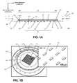
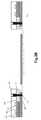
- FIG. 1Aprovides a schematic cross-sectional view of a reinforced composite stamp.
- FIGS. 1B and 1Care respectively optical image and scanning electron micrograph of the reinforced composite stamp schematically illustrated in 1 A, respectively.
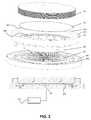
- FIG. 2provides schematic cross-sectional views of various transfer printing systems incorporating the composite stamps disclosed herein.
- FIG. 2Ashows a transfer printing tool head apparatus having a metal ring and metal screws that secures the composite stamp.
- FIG. 2Bshows a composite stamp vacuum-chucked to a transfer printing tool head apparatus by an intermediate metal apparatus.
- FIG. 2Cshows a composite stamp vacuum-chucked to a transfer printing tool head apparatus without an intermediate metal apparatus.
- FIG. 2Dshows a composite stamp vacuum-chucked to a transfer printing tool head apparatus by an intermediate elastomeric interposer.
- FIG. 3is a schematic view of a system of the present invention for molding a reinforced composite stamp of the present invention.
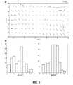
- FIG. 4provides measurements of the profile of a reinforced composite stamp that is subject to increasing levels of applied pressure to the stamp backing layer. Plotted is a measure of vertical displacement (mm) as a function of radial stamp position (mm).
- FIG. 5illustrates in-plane distortion measurements across a reinforced composite stamp, laminated against its own master.
- FIG. 5Ashow displacement vectors and
- FIG. 5Bprovide histogram plots of lateral displacement along x-direction (left side) and y-direction (right side).
- FIGS. 6A and Bprovide plots of placement accuracy measurements of silicon chiplets transferred onto a target substrate using a reinforced composite stamp.
- stamprefers to a device component for transfer, assembly and/or integration of structures and materials via printing, for example dry transfer contact printing.
- Composite stamps of the present inventionare particularly useful for pickup and release/print systems, wherein the stamp can be first laminated or contacted with a donor substrate to pickup micro- or nanostructures from that donor substrate and subsequently brought into contact with a receiving substrate to which it transfers the micro- or nanostructures.
- “Inked”refers to a stamp that has received micro- or nanostructures from a donor substrate.
- Inkingrefers to the step of pickup or transfer of micro- or nanostructures from a donor substrate to the stamp.
- “Substrate”refers to a structure or material on which, or in which, a process is conducted, such as patterning, assembly and/or integration of semiconductor elements.
- Substratesinclude, but are not limited to: (i) a structure upon which semiconductor elements are fabricated, deposited, transferred or supported; (ii) a device substrate, for example an electronic device substrate; (iii) a donor substrate having elements, such as semiconductor elements, for subsequent transfer, assembly or integration; and (iv) a target substrate for receiving printable structures, such as semiconductor elements.
- Compositerefers to a structure, material, layer, or device that comprises more than one component, such as more than one material and/or phase.
- composite patterning devices or “composite stamps”made from a deformable layer and a rigid support layer, wherein the deformable and support layers have different chemical compositions and mechanical properties.
- the deformable layeroptionally comprises a composite polymer layer comprising a combination of one or more polymer and a fiber, such as a glass or elastomeric fiber, particulate, such as nanoparticles or microparticles or any combinations of these.
- “Reinforced composite stamp”refers to a composite stamp having a reinforcement layer. Incorporation of reinforcement layers in composite stamps of the present invention is useful for achieving high yield, reliable and accurate transfer printing of semiconductor elements. Incorporation of reinforcement layers is useful for achieving long stamp lifetimes, and facilitating conformal contact between stamps of the present invention and substrates.
- Layerrefers to an element of a composite stamp. Exemplary layers have physical dimensions and mechanical properties which provide composite stamps capable of fabricating patterns on substrate surfaces having excellent fidelity and good placement accuracy. Layers of the present invention may be a continuous or unitary body or may be a collection of discontinuous bodies, such as a collection of relief features or protrusions. Layers of the present invention may have a homogenous composition or an inhomogeneous composition. An embodiment of the present invention provides a composite patterning device or composite stamp comprising a plurality of layers, such as a polymer layer, a reinforcement layer and a rigid backing layer.
- Layers in the present inventionmay be characterized in terms of their thickness along a layer alignment axis which extends through a patterning device, such as a layer alignment axis which is positioned orthogonal to a plane containing one or more contact surfaces.
- layers such as the reinforcement layermay be characterized by their geometric shape including orifice area, shape and position relative to the printable area of the composite stamp.
- Deformable layerrefers to an layer of material which can be stretched or deformed and return to substantially its original shape without substantial permanent deformation.
- Deformable layers of the present inventioninclude polymer layers, such as elastomer layers capable of undergoing substantially elastic deformations.
- Exemplary elastomers useful in deformable layers of the present inventionmay comprise polymers, copolymers, composite materials or mixtures of polymers and copolymers.
- Deformable layersmay also include dopants and other non-elastomeric materials and components.
- Elastomers useful in the present inventionmay include, but are not limited to, PDMS, h-PDMS, polybutadiene, polyisobutylene, poly(styrene-butadiene-styrene), polyurethanes, polychloroprene and silicones.
- “Reinforcement layer”refers to a material that imparts an additional influence on a desired mechanical property of the composite stamp, such as further reducing the deformable layer in-plane motion without adversely impacting vertical flexibility or elasticity.
- the reinforcement layercomprises a material that is distinct from the material of the deformable layer.
- the reinforcement layercorresponds to the deformable layer material, but whose polymer has been supplemented or doped with (i) fibers, such as glass fibers or polymeric fibers, (ii) particles, such as silicon particles and/or nanosized particles, and/or (iii) other structural enhancers.
- the reinforcement layerhelps prevents delamination of stamp elements during high yield use of the stamp.
- Relief featuresrefer to protrusions, extensions or projections on the external surface of the deformable layer, such as a three-dimensional relief pattern, that facilitates dry-transfer printing of semiconductor elements from a donor substrate to a target substrate.
- the relief features of the deformable layerdefine a printable surface area.
- Print surface areaor “region” refers to that portion of the stamp used to transfer structures from a donor substrate to a target substrate.
- Active surface regionis used interchangeably with “printable surface region.”
- “Rigid”refers to a mechanical property of a layer of the composite stamp that constrains in-plane deformation and unwanted motion of the deformable layer during any stage of transfer printing.
- a “rigid support layer”that is operably connected to the deformable layer permits vertical flexibility of the deformable layer and also minimizes unwanted in-plane motion of the deformable stamp.
- In planerefers to a plane that is parallel to a plane defined by the printable area of the composite stamp.
- “Vertical”refers to a direction that is orthogonal to the plane defined by the printable area of the composite stamp.
- “Vertically coincides”refers to an opening in the reinforcement layer that is positioned to encompass at least a portion of the relief features of the deformable layer (or the corresponding master mold from which the relief features are made), with the recognition that the opening and relief features are formed on different planes that are separated from each other by a vertical distance. In an aspect, all of the relief features vertically coincide with the opening in the reinforcement layer.
- “Anisotropic distribution”refers to a physical parameter whose magnitude depends on the direction in which the parameter is measured.
- the composite stampis designed so that the deformable layer motion is more constrained in plane than in a vertical (e.g., orthogonal) direction. This can be expressed by any number of mechanical parameters such as Young's modulus, flexural rigidity, or stiffness.
- Coefficient of thermal expansionrefers to a parameter which characterizes the change in size that a material undergoes upon experiencing a change in temperature.
- the present inventionprovides composite, multilayer patterning devices wherein thermal properties and physical dimensions of discrete layers are selected to provide a substantially symmetrical distribution of coefficients of thermal expansion about the center of the device along a layer alignment axis extending through the device.
- “Vacuum chuck”refers to a holder that uses vacuum to hold objects, and is particularly useful for creating a reversible connection where two parts that are held together by the vacuum chuck are readily released from each other when the vacuum is removed.
- “Lamination”refers to the process of bonding layers of a composite material or a process of producing contact between a first material or layer and a second layer or material (e.g, such as between the rigid backing and reinforcement layer, rigid backing and deformable layer, reinforcement layer and deformable layer, for example).
- Masterrefers to shaped surfaces used to mold corresponding replicas in polymers.
- the masteris a patterned silicon device having a three-dimensional relief pattern for generating a corresponding plurality of relief features in the deformable layer external surface.
- external surfaceof the deformable layer refers to the surface that is used to contact a donor and/or target substrate. Accordingly, internal surface of the deformable layer is that surface that makes contact with the rigid backing or the reinforcement layer.
- Pattern accuracyrefers to the ability of a pattern transfer method or device to generate a pattern in a selected region of a substrate. “Good placement” accuracy refers to methods and devices capable of generating patterning in a select region of a substrate with spatial deviations from the absolutely correct orientation less than or equal to 5 microns, particularly for generating patterns of semiconductor elements on target substrates.
- “Fidelity”refers to a measure of the similarity of a pattern transferred to a substrate surface and a relief pattern on a patterning device. Good fidelity refers to similarities between a pattern transferred to a substrate surface and a relief pattern on a patterning device characterized by deviations less than 100 nanometers.
- Young's modulusis a mechanical property of a material, device or layer which refers to the ratio of stress to strain for a given substance. Young's modulus may be provided by the expression;
- EYoung's modulus
- L 0the equilibrium length
- ⁇ Lthe length change under the applied stress
- Fthe force applied
- Athe area over which the force is applied.
- Young's modulusmay also be expressed in terms of Lame constants via the equation:
- Conformal contactrefers to contact established between surfaces and/or coated surfaces, which may be useful for fabricating structures on a substrate surface.
- conformal contactinvolves a macroscopic adaptation of one or more contact surfaces of a composite patterning device to the overall shape of a substrate surface.
- conformal contactinvolves a microscopic adaptation of one or more contact surfaces of a composite patterning device to a substrate surface leading to an intimate contact with out voids.
- conformal contactis intended to be consistent with use of this term in the art of dry transfer patterning. Conformal contact may be established between one or more bare contact surfaces of a composite patterning device and a substrate surface.
- conformal contactmay be established between one or more coated contact surfaces, for example contact surfaces having a transfer material such as a semiconductor element and/or patterning agent deposited thereon, of a composite patterning device and a substrate surface.
- patterning devices of the present inventionare capable of establishing conformal contact with flat surfaces.
- patterning devices of the present inventionare capable of establishing conformal contact with contoured surfaces.
- patterning devices of the present inventionare capable of establishing conformal contact with rough surfaces.
- patterning devices of the present inventionare capable of establishing conformal contact with smooth surfaces.
- Flexural rigidityis a mechanical property of a material, device or layer which refers to the ability of a material, device or layer to be deformed. Flexural rigidity may be provided by the expression:
- Dflexural rigidity
- EYoung's modulus
- hthickness
- vthe Poisson ratio
- Flexural rigiditymay be expressed in units of force multiplied by unit length, such as Nm.
- Polymerrefers to a molecule comprising a plurality of repeating chemical groups, typically referred to as monomers. Polymers are often characterized by high molecular masses. Polymers useable in the present invention may be organic polymers or inorganic polymers and may be in amorphous, semi-amorphous, crystalline or partially crystalline states. Polymers may comprise monomers having the same chemical composition or may comprise a plurality of monomers having different chemical compositions, such as a copolymer. Cross linked polymers having linked monomer chains are particularly useful for some applications of the present invention.
- Polymers useable in the methods, devices and device components of the present inventioninclude, but are not limited to, plastics, elastomers, thermoplastic elastomers, elastoplastics, thermostats, thermoplastics and acrylates.
- Exemplary polymersinclude, but are not limited to, acetal polymers, biodegradable polymers, cellulosic polymers, fluoropolymers, nylons, polyacrylonitrile polymers, polyamide-imide polymers, polyimides, polyarylates, polybenzimidazole, polybutylene, polycarbonate, polyesters, polyetherimide, polyethylene, polyethylene copolymers and modified polyethylenes, polyketones, poly(methyl methacrylate, polymethylpentene, polyphenylene oxides and polyphenylene sulfides, polyphthalamide, polypropylene, polyurethanes, styrenic resins, sulphone based resins, vinyl-based resins or any combinations of these.
- Prepolymerrefers to a material that is capable of undergoing polymerization but that is in its unpolymerized liquid or gel state.
- Useful prepolymersare those of sufficiently low viscosity such that they are readily introduced to the stamp-forming chamber of the composite stamp generating devices disclosed herein.
- Elastomerrefers to a polymeric material which can be stretched or deformed and return to its original shape without substantial permanent deformation. Elastomers commonly undergo substantially elastic deformations. Exemplary elastomers useful in the present invention may comprise, polymers, copolymers, composite materials or mixtures of polymers and copolymers. Elastomeric layer refers to a layer comprising at least one elastomer. Elastomeric layers may also include dopants and other non-elastomeric materials.
- Elastomers useful in the present inventionmay include, but are not limited to, silicon containing polymers such as polysiloxanes including poly(dimethyl siloxane) (i.e PDMS and h-PDMS), poly(methyl siloxane), partially alkylated poly(methyl siloxane), poly(alkyl methyl siloxane) and poly(phenyl methyl siloxane), silicon modified elastomers, thermoplastic elastomers, styrenic materials, olefenic materials, polyolefin, polyurethane thermoplastic elastomers, polyamides, synthetic rubbers, polyisobutylene, poly(styrene-butadiene-styrene), polyurethanes, polychloroprene and silicones.
- silicon containing polymerssuch as polysiloxanes including poly(dimethyl siloxane) (i.e PDMS and h-PDMS), poly(methyl siloxane), partially alky
- contact surfacerefers to one or more surfaces of the composite stamps that contacts a substrate undergoing processing, for example during inking, transfer printing, assembly or integration processes.
- the external surfaces of the deformable layerprovides one or more contact surfaces, receiving surfaces or printing surfaces of composite stamps of the present invention.
- relief features of the deformable layerprovide one or more contact surfaces, receiving surfaces or printing surfaces composite stamps of the present invention.
- semiconductor elementand “semiconductor structure” are used synonymously and broadly refer to a semiconductor material, structure, device and/or component of a device.
- Semiconductor elementsinclude high quality single crystalline and polycrystalline semiconductors, semiconductor materials fabricated via high temperature processing, doped semiconductor materials, organic and inorganic semiconductors and composite semiconductor materials and structures having one or more additional semiconductor components and/or non-semiconductor components, such as dielectric layers or materials and/or conducting layers or materials.
- Semiconductor elementsinclude semiconductor devices and device components including, but not limited to, transistors, photovoltaics including solar cells, diodes, light emitting diodes, lasers, p-n junctions, photodiodes, integrated circuits, and sensors
- semiconductorrefers to any material that is a material that is an insulator at a very low temperature, but which has a appreciable electrical conductivity at a temperatures of about 300 Kelvin. In the present description, use of the term semiconductor is intended to be consistent with use of this term in the art of microelectronics and electronic devices.
- Semiconductors useful in the present inventionmay comprise element semiconductors, such as silicon, germanium and diamond, and compound semiconductors, such as group IV compound semiconductors such as SiC and SiGe, group III-V semiconductors such as AlSb, AlAs, Aln, AlP, BN, GaSb, GaAs, GaN, GaP, InSb, InAs, InN, and InP, group III-V ternary semiconductors alloys such as Al x Ga 1-x As, group II-VI semiconductors such as CsSe, CdS, CdTe, ZnO, ZnSe, ZnS, and ZnTe, group I-VII semiconductors CuCl, group IV-VI semiconductors such as PbS, PbTe and SnS, layer semiconductors such as PbI 2 , MoS 2 and GaSe, oxide semiconductors such as CuO and Cu 2 O.
- group IV compound semiconductorssuch as SiC and SiGe
- group III-V semiconductorssuch as AlSb, Al
- semiconductorincludes intrinsic semiconductors and extrinsic semiconductors that are doped with one or more selected materials, including semiconductor having p-type doping materials and n-type doping materials, to provide beneficial electronic properties useful for a given application or device.
- semiconductorincludes composite materials comprising a mixture of semiconductors and/or dopants.
- Specific semiconductor materials useful for in some applications of the present inventioninclude, but are not limited to, Si, Ge, SiC, AlP, AlAs, AlSb, GaN, GaP, GaAs, GaSb, InP, InAs, GaSb, InP, InAs, InSb, ZnO, ZnSe, ZnTe, CdS, CdSe, ZnSe, ZnTe, CdS, CdSe, CdTe, HgS, PbS, PbSe, PbTe, AlGaAs, AlInAs, AlInP, GaAsP, GaInAs, GaInP, AlGaAsSb, AlGaInP, and GaInAsP.
- Porous silicon semiconductor materialsare useful for applications of the present invention in the field of sensors and light emitting materials, such as light emitting diodes (LEDs) and solid state lasers.
- Impurities of semiconductor materialsare atoms, elements, ions and/or molecules other than the semiconductor material(s) themselves or any dopants provided to the semiconductor material. Impurities are undesirable materials present in semiconductor materials which may negatively impact the electronic properties of semiconductor materials, and include but are not limited to oxygen, carbon, and metals including heavy metals. Heavy metal impurities include, but are not limited to, the group of elements between copper and lead on the periodic table, calcium, sodium, and all ions, compounds and/or complexes thereof.
- Operably connectedrefers to a configuration of layers and/or device components of composite patterning devices of the present invention such that functionality of the components or layers are preserved when connected.
- Operably connected layers or device componentsrefers to an arrangement wherein a force applied to a layer or device component is transmitted to another layer or device component.
- Operably connected layers or device componentsmay be in contact, such as layers having internal and/or external surfaces in physical contact.
- operably connected layers or device componentsmay be connected by one or more connecting layers, such as thin metal layers or reinforcement layers, positioned between the internal and/or external surfaces of two layers or device components, or that run between two or more layers or components.
- a rigid layer and a reinforcement layerare “operably connected” such that the stamp with the reinforcement layer is capable of withstanding a higher activation force without bowing or having the rigid layer fracturing or otherwise damaged compared to a stamp without the reinforcement layer.
- stamps for dry transfer contact printing applicationsare minimizing mechanical distortions induced by thermal contraction during stamp fabrication or application of in-plane stress forces during printing processes. Such distortions can significantly impact the fidelity and accuracy of the printing.
- a thin glass backing materialcan be effectively integrated into a composite stamp for the purpose of preventing in-plane mechanical deformation of the stamp.
- the thickness of the glass backing layeris less than 300 ⁇ m thick (e.g., about 100 ⁇ m to 200 ⁇ m thick)
- the elastomeric stampcan conform to the surface of uneven substrates such as flexible plastic substrates and substrate prepatterned with electronic devices and components.
- Such thin glass backing sheetsare relatively fragile, and therefore, may be subject to mechanical failure during printing. This attribute impedes use of thin glass backing materials in conventional composite stamps for dry transfer contact printing.
- a reinforcement layeris incorporated into a composite stamp of the present invention that effectively mitigates the fragility concern, while retaining the performance benefits accessed by use of a thin glass backing.
- a two-step molding processallows fabrication of the composite stamps in a reliable manner that addresses the fragility issue.
- a thick polydimethylsiloxane (PDMS) cylindrical blockis molded using an aluminum mold as described hereinafter. This thick PDMS block is used to temporarily hold the thin glass backing sheet during the composite stamp molding process as discussed in more detail hereinafter.
- a reinforcement layere.g., fiberglass
- a reinforcement layeris added to improve the mechanical properties and placement repeatability with printing by the reinforced composite stamps.
- FIGS. 1 through 3detail aspects of the reinforced composite stamp, printing devices and devices for making the reinforced composite stamps.
- the systemsare subjected to various testing and printing and FIGS. 4 through 6 summarize results of exemplary tests and indicate the systems achieve consistent accuracy, reliability and satisfy various other desired objectives.
- FIG. 1Aprovides a schematic cross-sectional view of an exemplary reinforced composite stamp 100 of the present invention.
- the composite stampcomprises a deformable layer 70 , a reinforcement layer 120 , and a rigid support layer 150 .
- An array of relief features 105are defined on the external surface 80 of the deformable layer 70 to facilitate selective transfer of printed structures, such as semiconductor elements.
- Array of relief features 105may comprise a relief pattern providing selective printing or patterning functionality.
- External surface 80is the surface of deformable layer 70 configured such that it is that is capable of contacting donor or target substrates for dry-transfer printing processes, for example providing a contact surface, printing surface or receiving surface of stamp 100 for dry transfer contact printing.
- the deformable layer 70also has an internal surface 75 that faces rigid support layer 150 . As shown in FIG. 1A , internal surface 75 is connected to the rigid support layer 150 and configured such that it does not directly contact a donor or target substrate during printing processing.
- deformable layer 70is an elastomer layer and rigid support layer 150 is a thin glass backing of composite stamp 100 .
- Rigid support layer 150has bottom surface 175 , top surface 185 , and outer edges 195 .
- reinforcement layer 120is positioned on top of rigid support layer 150 (e.g., facing top surface 185 ).
- reinforcement layer 120connected to both the top surface 185 and bottom surface 175 of rigid support layer 150 .
- reinforcement layeris disposed at least partially between the deformable or elastomer layer 70 and outer edge 195 of rigid backing layer 150 , such as by continuing past outer edge 195 toward a stamp mounting element, such as mounting flange 121 .
- reinforcement layer 120is connected to the bottom surface 175 of rigid support layer 150 and has an opening 197 (schematically illustrated in FIG. 1B with a dashed line) that is vertically coincident to the plurality of relief features 105 .
- the area of overlap between the reinforcement layer and the rigid support layercorresponds to the surface area of outer edge region 160 .
- the composite stamp 100is reinforced with the reinforcement layer 120 positioned such that it is partially disposed between deformable layer 70 and rigid support layer 150 .
- Reinforcement layer 120is configured to support and provide reinforcement to rigid support layer 150 , thereby conferring enhanced overall mechanical stability and stamp lifetime.
- reinforcement layer 120is a ring of woven fiberglass that is only partially disposed between the deformable layer 70 and the rigid support layer 150 .
- reinforcement layer 120is bonded to the outer edge region 160 of rigid support layer 150
- deformable layer 70is bound to a central region 170 of rigid support layer 150 .
- central region 170corresponds to the area of opening 197 in the reinforcement layer 120 .
- reinforcement layer 120is embedded in deformable layer 70 .
- composite stamp 100is operably connected to an annular mounting flange 121 such that reinforcement layer 120 and/or deformable layer 70 bridges the gap between the rigid support layer 150 and the annular mounting flange 121 .
- the annular mounting flange 121is populated with a circular array of mounting or registration features such as cylindrical perforations 122 .
- the direction of “lateral” and “vertical”is illustrated in FIG. 1A by the arrows labeled with the relevant dimension or direction description.
- the lateral dimension or directioncorresponds to the radial dimension or direction.
- the rigid backing thicknessis labeled 510 and is the distance between the ends of the two associated facing arrows.
- the thickness of the deformable layeris labeled 520 and is the distance between the ends of the two associated facing arrows.
- the deformable layer thicknesscorresponds to the separation distance between the uppermost relief feature on a mold used to form the relief features and the rigid backing.
- deformable layer thicknessis described in terms of thickness 520 plus the height of a relief feature on the deformable layer.
- relief features 105 of deformable layer 70are defined via a molding process using a master wafer mold (e.g., see 402 of FIG. 3 ) that is patterned with a desired three-dimensional relief pattern.
- the master mold patternis optionally obtained by a photo-defined pattern in a 5 to 100 ⁇ m photo-resist layer on the surface of a mechanical grade silicon wafer.
- relief features 105are provided with physical dimensions and positions selected to serve a number of functions useful for printing-based processing, including, but not limited to, stabilization patterns 110 for stabilizing the printable area or printing surface area 85 , transfer posts 111 to facilitate lift-off and release of printed elements, anti-sagging posts 112 to minimize stamp sagging, and alignment or registration features (not shown, such as lock-and-key features) for enhancing stamp alignment during printing.
- stabilization patterns 110for stabilizing the printable area or printing surface area 85
- transfer posts 111to facilitate lift-off and release of printed elements
- anti-sagging posts 112to minimize stamp sagging
- alignment or registration featuresnot shown, such as lock-and-key features
- the reinforcement layer 120is positioned to contact the rigid support layer 150 at an outer edge region 160 (e.g., the reinforcement layer extends into the rigid support layer outer edge region by a distance corresponding to 160 ).
- the portion of deformable layer 70 that is positioned inside the reinforcement layer 120 (e.g., within opening 197 )is referred to as the inner region 170 .
- the relative positions of the outer edge region 160 and inner region 170is selected for a specific processing application.
- outer edge region 160 and inner region 170are selected such that a substantial portion of the printing region 85 is vertically coincident to opening 197 so as to provide optical transparency and vertical flexibility of printing region 85 while reinforcement layer 120 maintains in-plane rigidity and mechanical robustness of composite stamp considering the fragility of the rigid support layer 150 (e.g., less than about 300 ⁇ m thick).
- the outer edge 160is entirely outside the printing surface area 85 , such as a printing surface area that is defined by the outer footprint of array of relief features 105 .
- the outer edge regionis defined as a range of outermost surface area of the rigid support layer 150 , such as the outermost surface area that comprises less than 20%, less than 10% or less than 5% the surface area of the rigid support layer surface that faces the reinforcement layer (e.g., the top or bottom surface of the rigid support layer).
- An important optional feature of a reinforced composite stampis the ability to contact donor or target substrates having a larger surface than the reinforced composite stamp.
- a number of composite stamps and related printing systems known in the artare designed to interact with surfaces that are equal or less than the surface area of the composite stamp. This is a significant disadvantage for step-and-repeat processing where the stamp is used to repeatedly print to a large area of a target substrate.
- FIG. 1AOne design strategy for ensuring adequate clearance between the composite stamp (and particularly the print tool head to which the stamp is mounted) is illustrated in FIG. 1A .
- the vertical section or flange connector 130enables the stamp patterned surface 105 to be located in a recessed plane.
- This stamp configurationprovides a number of benefits, including: (i) facilitating mounting of the stamp by providing geometrical clearance, (ii) and enhancing out-of-plane vertical motion of the stamp's printing surface useful for establishing conformal contact with a substrate surface.
- a protruding reinforcement ring 125is also provided to reduce mechanical stress at the interface between the deformable layer 70 and edge of internal surface 75 and the edge of the rigid support layer 150
- rigid support layer 150has a composition and physical dimensions provided to prevent in-plane mechanical deformations of the stamps in the lateral direction. This configuration ensures that mechanical distortions induced by thermal contraction during stamp fabrication or application of in-plane stress forces during printing are minimized.
- the rigid support layer 150is a glass layer having a thickness selected to be less than 500 ⁇ m thick, and optionally a thickness of 100 to 300 ⁇ m. Use of such a thin rigid support layer 150 comprising a glass layer as provided in the reinforced configuration shown in FIG. 1A is useful to achieve the capability to conform to the surface of uneven substrates such as flexible plastic substrates and substrates prepatterned with devices and components, while minimizing in-plane deformation during printing that can undermine transfer accuracy and pattern fidelity.
- FIGS. 1B and 1Crespectively, provide an optical image and a scanning electron micrograph of reinforced composite stamps.
- the reinforced composite stamphas a pattern of relief features comprising a plurality of posts having a rectangular cross section.
- the postsare provided in a 30 ⁇ 30 mm array arrangement with an average distance between adjacent posts equal to 370 microns.
- the composite stamp glass backingis round shaped with an overall diameter of 76.2 mm and a thickness of 200 microns.
- the woven glass fiber ring reinforcementconsist of Style 120 E-Glass fiberglass fabrics having a weight density of ⁇ 30z/Yd 2 , and an average thickness of 90-115 ⁇ m, with a 4-Harness Satin style weave pattern.
- the reinforcement ringis laser cut into a perforated ring shape having the following physical dimensions: inner diameter of 54 mm, outer diameter of 120 mm, holes diameters of 2 mm.
- FIGS. 2A-Dprovides a schematic cross-sectional view of a reinforced composite stamp illustrating different examples of how a stamp of FIG. 1 is attached to a transfer printing tool head apparatus 300 .
- Such a systemcan be used for a wide variety of printing methods, including dry transfer printing methods related to conformal contact with a target or a donor substrate, illustrated by 400 in FIG. 2C , where the dashed lines indicate the target or donor substrate extends and has a surface area that is larger than the printable area 85 or surface area of deformable layer 70 .
- the stamp and mounting designensures there is adequate clearance distance 320 between a target substrate 400 positioned in contact with the relief features and the apparatus to which the stamp is mounted, thereby facilitating printing to a target substrate that has a surface area that is larger than the printable surface area of the composite stamp.
- FIG. 2Aillustrates a reinforced composite stamp that is connected to the print tool head 300 , and specifically the tool head receiving surface 310 by a fastener 201 (exemplified by a metal screw) that extends through holding platform 200 , stamp flange 121 and tool receiving surface 310 .
- a fastener 201(exemplified by a metal screw) that extends through holding platform 200 , stamp flange 121 and tool receiving surface 310 .
- the fasteneris a screw
- the receiving surfaceis threaded to secureably receive the screw.
- the fasteneris oriented in the other direction, such that it extends through the tool head apparatus and at least partially through the holding platform 300 .
- FIG. 2Bis a schematic cross-section showing the reinforced composite stamp vacuum-chucked to a transfer printing tool head apparatus ( 300 ).
- a vacuum chuck 305is operably connected to vacuum grooves 302 to hold an upper portion and a lower portion positioned on either side of the stamp flange 130 .
- a holding platform 200is shaped to have a holder receiving chamber 220 in which flange 121 is at least partially disposed. A portion of the holder 200 contacts vacuum chuck 305 vacuum grooves ( 302 ) defined on the receiving surface 310 of the tool head 300 .
- An optional fastener 201is shown as a dowel pin. For further stability, the dowel pins 201 are arranged in a circular array to provide a first-pass pre-alignment of the composite stamps.
- FIG. 2Cis a schematic cross-section of a reinforced composite stamp vacuum-chucked to a transfer printing tool head apparatus ( 300 ).
- vacuum grooves ( 302 )are defined on the receiving surface 310 of the tool head apparatus ( 300 ).
- the composite stamp mounting flange 121is directly vacuum chucked to the tool head apparatus 300 (compare to FIG. 2B where the vacuum chuck directly vacuums holding platform 200 ).
- FIG. 2Dis a schematic cross-section of a reinforced composite stamp vacuum-chucked to a transfer printing tool head apparatus ( 300 ).
- vacuum grooves ( 302 )are defined in an intermediate elastomeric holder ( 350 ) to provide a ‘soft’ mechanical connection between the tool head 300 and the reinforced composite stamp.
- FIG. 3is a schematic illustration of a set of parts used in the process of making or molding reinforced composite stamps.
- One example of the steps used to make a reinforced composite stampare as follows:
- a master 402for example a patterned master is fabricated using standard techniques, such as a UV photo-lithographic process (as described in published lithography literature; see, e.g., US Pat. Pub. No. 20060286785 to Rogers et al.).
- master 402is a patterned silicon wafer having relief features corresponding to the relief feature pattern desired for the deformable stamp patterned surface.
- the master 402is placed with the surface 425 having the relief feature pattern facing down in a wafer holder subassembly 403 .
- An example wafer holder subassembly 403is machined stainless steel. As shown in FIG. 3 , the wafer holder subassembly 403 has vertical adjusters 403 a and 403 b , such as orifices for receiving adjustment bolts, for example, to provide controlled separation.
- a fastener 401depicted as a machined Teflon block is then screwed-in to secure in place the master 402 in the wafer holder 403 .
- Other fastenersmay be employed to hold the master in place including, but not limited to, clamps, levers, springs, screw-plates, etc.
- a rigid support layer 150such as a thin glass wafer, is placed on the surface of a holder.
- useful holders for this aspectinclude an elastomeric holder or elastomeric chuck 405 that is a sub-part of the stamp mold subassembly 406 .
- a vacuum lineis briefly connected to the vacuum chuck exhaust port 407 in order to insure a proper lamination of the thin (e.g., ⁇ 100 to 500 ⁇ m) rigid support layer 150 , depicted in FIG. 3 as a glass disk.
- a reinforcement layer 120such as a ring of woven fiberglass, is placed onto the thin glass disk.
- the wafer holder subassembly(e.g., fastener 401 , master 402 , holder 403 ) is coupled to the stamp mold subassembly 150 , 405 - 407 .
- a set of vertical adjusters all around wafer holder 403shown as bolts 403 a and 403 b are adjusted to maintain a greater than about 1 mm separation gap between the master surface 425 and the surface of the rigid support layer surface 150 .
- the combined assembly of the wafer holder subassembly 401 - 403 and stamp mold subassembly 404 - 407is placed inside a modified vacuum dessicator containing a plastic cup filled with freshly mixed 2-part elastomer mixture (also referred herein as “prepolymer” mixture).
- a plastic cupfilled with freshly mixed 2-part elastomer mixture (also referred herein as “prepolymer” mixture).
- prepolymeralso referred herein as “prepolymer” mixture.
- the plastic cupis mechanically coupled to a vacuum sealed rotary drive which enables the operator to empty the plastic cup under vacuum.
- the dessicatoris connected to a vacuum line in order to remove air and degas the elastomer 2-part mixture.
- the degassed elastomer mixture or prepolymeris introduced to the stamp-forming chamber 440 that is between said master and said rigid backing faces via the openings 406 a in the stamp mold subassembly (illustrated as ports).
- the dessicatoris vented to air and the combined wafer—stamp mold assembly of the wafer holder is removed.
- the adjustment bolts 403 aare un-screwed and the set of bolts 403 b are tightened in order to bring the silicon master in close proximity (e.g., ⁇ 500 ⁇ m) with the thin glass backing. During this process, any excess elastomer mixture exhausts through the stamp mold assembly openings or ports 406 a . Hard-stop spacers built in the stamp mold subassembly enable a fine control of the final separation gap.
- the elastomer mixtureis cured inside an oven, for example by following the elastomer manufacturer's recommendations.
- Conventional ovens, ultraviolet rays, infrared rays and other means for curing as appropriate for the particular prepolymer mixture in the stamp-forming chamberare employed.
- the resultant cured elastomer mixture that makes up the reinforced composite stampis taken out of the oven, cooled in air at room temperature or in a cooled environment.
- the set of bolts 403 a and 403 bare loosened to separate the wafer holder subassembly 401 - 403 and the stamp mold subassembly 404 - 407 .
- the vacuum chuck exhaust port 407is briefly connected to a pressurized N 2 gas line in order to facilitate the separation of the reinforced composite stamp from the stamp mold subassembly.
- FIG. 4provides measurements of the profile of a reinforced composite stamp of the invention subject to different pressure applied to the stamp's rigid support layer.
- the rigid support layeris a glass backing disk with a thickness of ⁇ 100 ⁇ m.
- This graphwas obtained by recording the focal plane position using a high resolution CCD camera and by maintaining the camera focus point on the stamp patterns.
- FIG. 5provides in-plane distortion measurements across a reinforced composite stamp of the invention laminated against its own master.
- a composite stamp with an array of 50 ⁇ 50 ⁇ m postswas fabricated and mounted on a transfer printing tool head.
- the stampwas precisely aligned optically and laminated on the silicon master wafer which was used to fabricate the stamp.
- an array of high resolution optical imageswas recorded to capture local misalignments between the composite stamp and its master.
- These imageswere then processed using an image analysis algorithm developed using Matlab image processing toolbox.
- the extracted local misalignment dataare presented in FIG. 5 as quiver ( FIG. 5A ) and histogram plots in the x-direction ( FIG. 5B ) and y-direction ( FIG. 5C ).
- the motion algorithm of the tool printing headwas optimized in order to obtain consistent stamp laminations and de-laminations.
- FIG. 6provides placement accuracy measurements of silicon chiplets transferred onto a target substrate using a reinforced composite stamp of the present invention. These measurements were obtained by analyzing a collection of images acquired using a high resolution CCD camera) and analyzed using a similar image analysis algorithm. Local metal alignment marks were defined using standard semiconductor process onto the surface of a target glass wafer. The misalignment results are reported on a color coded type ( FIG. 6A ) and histogram ( FIG. 6B ) plots. These results indicate that the presented reinforced composite stamps are capable of transferring a large array (1024 in this case) of semiconductor chiplets with a placement accuracy that is better than about 4 ⁇ m at 3 sigma.
- the placement accuracy in the present examplemay be limited by the alignment accuracy of the printer used to record this set of data (limited by the resolution of the dry transfer printer linear and rotary stages).
Landscapes
- Engineering & Computer Science (AREA)
- Chemical & Material Sciences (AREA)
- Nanotechnology (AREA)
- Physics & Mathematics (AREA)
- General Physics & Mathematics (AREA)
- Crystallography & Structural Chemistry (AREA)
- Manufacturing & Machinery (AREA)
- Condensed Matter Physics & Semiconductors (AREA)
- Mathematical Physics (AREA)
- Theoretical Computer Science (AREA)
- Computer Hardware Design (AREA)
- Microelectronics & Electronic Packaging (AREA)
- Power Engineering (AREA)
- Printing Plates And Materials Therefor (AREA)
- Exposure Of Semiconductors, Excluding Electron Or Ion Beam Exposure (AREA)
Abstract
Description
ΔL=αL0ΔT (I)
- U.S. Pat. No. 6,062,133 May 16, 2000 Blalock
- U.S. Pat. No. 6,829,988 Dec. 14, 2004 George et al.
- U.S. Pat. No. 5,947,027 Dec. 7, 1999 Burgin et al.
- U.S. Pat. No. 6,876,081 Apr. 5, 2005 Chow
- U.S. Pat. No. 6,855,378 Feb. 15, 2005 Narang
- U.S. Pat. No. 6,740,543 May 24, 2005 Rutiser
- U.S. Pat. No. 4,503,335 Mar. 5, 1985 Takahashi
- U.S. Pat. No. 6,918,982 Jul. 19, 2005 Afzali-Ardakani et al.
- U.S. Pat. No. 7,296,519 Nov. 20, 2007 Dona et al.
- U.S. Pat. No. 7,295,256 Nov. 13, 2007 Kim
- U.S. Pat. No. 6,976,424 Dec. 20, 2005 Bruno et al.
- U.S. Pat. No. 6,881,366 Apr. 19, 2005 Hougham et al.
- U.S. Pat. No. 6,792,856 Sep. 21, 2004 Hall et al.
- U.S. Pat. No. 6,521,489 Feb. 18, 2003 Duthaler et al.
- U.S. Pat. No. 5,937,758 Aug. 17, 1999 Maracas et al.
- U.S. Pat. No. 5,669,303 Sep. 23, 1997 Maracas et al.
- U.S. Pat. No. 5,512,131 Apr. 30, 1996 Kumar et al.
- U.S. Ser. No. 11/423,192, Khang et al., “Pattern Transfer Printing By Kinetic Control Of Adhesion To An Elastomeric Stamp.”
- U.S. Ser. No. 11/421,654, Khang et al., “Printable Semiconductor Structures An Related Methods Of Making And Assembling.”
- U.S. Ser. No. 11/145,574, Khang et al., “Methods And Devices For Fabricating And Assembling Printable Semiconductor Elements.”
- U.S. Ser. No. 11/001,689, Jeon et al., “Methods and Device For Fabricating Three-Dimensional Nanoscale Structures.”
- U.S. Pat. No. 7,195,733, Rogers et al., “Composite patterning devices for soft lithography.”
Claims (69)
Priority Applications (5)
| Application Number | Priority Date | Filing Date | Title |
|---|---|---|---|
| US12/177,963US7927976B2 (en) | 2008-07-23 | 2008-07-23 | Reinforced composite stamp for dry transfer printing of semiconductor elements |
| TW098124599ATWI396621B (en) | 2008-07-23 | 2009-07-21 | Reinforced composite stamp for dry transfer printing of semiconductor elements |
| EP09800920.2AEP2311073B1 (en) | 2008-07-23 | 2009-07-22 | Reinforced composite stamp for dry transfer printing of semiconductor elements |
| PCT/US2009/051350WO2010011713A1 (en) | 2008-07-23 | 2009-07-22 | Reinforced composite stamp for dry transfer printing of semiconductor elements |
| KR1020117004225AKR101850156B1 (en) | 2008-07-23 | 2009-07-22 | Reinforced composite stamp for dry transfer printing of semiconductor elements |
Applications Claiming Priority (1)
| Application Number | Priority Date | Filing Date | Title |
|---|---|---|---|
| US12/177,963US7927976B2 (en) | 2008-07-23 | 2008-07-23 | Reinforced composite stamp for dry transfer printing of semiconductor elements |
Publications (2)
| Publication Number | Publication Date |
|---|---|
| US20100018420A1 US20100018420A1 (en) | 2010-01-28 |
| US7927976B2true US7927976B2 (en) | 2011-04-19 |
Family
ID=41567480
Family Applications (1)
| Application Number | Title | Priority Date | Filing Date |
|---|---|---|---|
| US12/177,963Active2029-11-18US7927976B2 (en) | 2008-07-23 | 2008-07-23 | Reinforced composite stamp for dry transfer printing of semiconductor elements |
Country Status (5)
| Country | Link |
|---|---|
| US (1) | US7927976B2 (en) |
| EP (1) | EP2311073B1 (en) |
| KR (1) | KR101850156B1 (en) |
| TW (1) | TWI396621B (en) |
| WO (1) | WO2010011713A1 (en) |
Cited By (167)
| Publication number | Priority date | Publication date | Assignee | Title |
|---|---|---|---|---|
| US8333860B1 (en) | 2011-11-18 | 2012-12-18 | LuxVue Technology Corporation | Method of transferring a micro device |
| US8349116B1 (en) | 2011-11-18 | 2013-01-08 | LuxVue Technology Corporation | Micro device transfer head heater assembly and method of transferring a micro device |
| WO2013010113A1 (en)* | 2011-07-14 | 2013-01-17 | The Board Of Trustees Of The University Of Illinois | Non-contact transfer printing |
| US8383506B1 (en) | 2012-07-06 | 2013-02-26 | LuxVue Technology Corporation | Method of forming a compliant monopolar micro device transfer head with silicon electrode |
| US20130069275A1 (en)* | 2011-09-20 | 2013-03-21 | Etienne Menard | Printing transferable components using microstructured elastomeric surfaces with pressure modulated reversible adhesion |
| US8415771B1 (en) | 2012-05-25 | 2013-04-09 | LuxVue Technology Corporation | Micro device transfer head with silicon electrode |
| US8415768B1 (en) | 2012-07-06 | 2013-04-09 | LuxVue Technology Corporation | Compliant monopolar micro device transfer head with silicon electrode |
| US8415767B1 (en) | 2012-07-06 | 2013-04-09 | LuxVue Technology Corporation | Compliant bipolar micro device transfer head with silicon electrodes |
| US8426227B1 (en) | 2011-11-18 | 2013-04-23 | LuxVue Technology Corporation | Method of forming a micro light emitting diode array |
| US8518204B2 (en) | 2011-11-18 | 2013-08-27 | LuxVue Technology Corporation | Method of fabricating and transferring a micro device and an array of micro devices utilizing an intermediate electrically conductive bonding layer |
| US8569115B1 (en) | 2012-07-06 | 2013-10-29 | LuxVue Technology Corporation | Method of forming a compliant bipolar micro device transfer head with silicon electrodes |
| US8573469B2 (en) | 2011-11-18 | 2013-11-05 | LuxVue Technology Corporation | Method of forming a micro LED structure and array of micro LED structures with an electrically insulating layer |
| WO2014000024A1 (en)* | 2012-06-26 | 2014-01-03 | University Of South Australia | Apparatus for fabricating microstructured devices |
| WO2014093243A1 (en)* | 2012-12-14 | 2014-06-19 | LuxVue Technology Corporation | Micro pick up array with integrated pivot mount |
| US20140169924A1 (en)* | 2012-12-14 | 2014-06-19 | LuxVue Technology Corporation | Micro device transfer system with pivot mount |
| US8791474B1 (en) | 2013-03-15 | 2014-07-29 | LuxVue Technology Corporation | Light emitting diode display with redundancy scheme |
| US8791530B2 (en) | 2012-09-06 | 2014-07-29 | LuxVue Technology Corporation | Compliant micro device transfer head with integrated electrode leads |
| US8835940B2 (en) | 2012-09-24 | 2014-09-16 | LuxVue Technology Corporation | Micro device stabilization post |
| US8928021B1 (en) | 2013-06-18 | 2015-01-06 | LuxVue Technology Corporation | LED light pipe |
| US8933433B2 (en) | 2012-07-30 | 2015-01-13 | LuxVue Technology Corporation | Method and structure for receiving a micro device |
| US8941215B2 (en) | 2012-09-24 | 2015-01-27 | LuxVue Technology Corporation | Micro device stabilization post |
| US8987765B2 (en) | 2013-06-17 | 2015-03-24 | LuxVue Technology Corporation | Reflective bank structure and method for integrating a light emitting device |
| US9029880B2 (en) | 2012-12-10 | 2015-05-12 | LuxVue Technology Corporation | Active matrix display panel with ground tie lines |
| US9035279B2 (en) | 2013-07-08 | 2015-05-19 | LuxVue Technology Corporation | Micro device with stabilization post |
| US9034754B2 (en) | 2012-05-25 | 2015-05-19 | LuxVue Technology Corporation | Method of forming a micro device transfer head with silicon electrode |
| US20150140220A1 (en)* | 2013-11-20 | 2015-05-21 | Thomas W. Palone | Method for forming a non-deformable patterned template |
| US9087764B2 (en) | 2013-07-26 | 2015-07-21 | LuxVue Technology Corporation | Adhesive wafer bonding with controlled thickness variation |
| US9095980B2 (en) | 2013-02-25 | 2015-08-04 | LuxVue Technology Corporation | Micro pick up array mount with integrated displacement sensor |
| US9105714B2 (en) | 2012-12-11 | 2015-08-11 | LuxVue Technology Corporation | Stabilization structure including sacrificial release layer and staging bollards |
| US9105492B2 (en) | 2012-05-08 | 2015-08-11 | LuxVue Technology Corporation | Compliant micro device transfer head |
| US9111464B2 (en) | 2013-06-18 | 2015-08-18 | LuxVue Technology Corporation | LED display with wavelength conversion layer |
| US9136161B2 (en) | 2013-06-04 | 2015-09-15 | LuxVue Technology Corporation | Micro pick up array with compliant contact |
| US9153548B2 (en) | 2013-09-16 | 2015-10-06 | Lux Vue Technology Corporation | Adhesive wafer bonding with sacrificial spacers for controlled thickness variation |
| US9153171B2 (en) | 2012-12-17 | 2015-10-06 | LuxVue Technology Corporation | Smart pixel lighting and display microcontroller |
| US9159700B2 (en) | 2012-12-10 | 2015-10-13 | LuxVue Technology Corporation | Active matrix emissive micro LED display |
| US9162880B2 (en) | 2012-09-07 | 2015-10-20 | LuxVue Technology Corporation | Mass transfer tool |
| US9166114B2 (en) | 2012-12-11 | 2015-10-20 | LuxVue Technology Corporation | Stabilization structure including sacrificial release layer and staging cavity |
| US9178123B2 (en) | 2012-12-10 | 2015-11-03 | LuxVue Technology Corporation | Light emitting device reflective bank structure |
| WO2015184088A1 (en)* | 2014-05-28 | 2015-12-03 | The Trustees Of The University Of Pennsylvania | Surfaces with tunable adhesion based on composite structures and methods of making the same |
| US9217541B2 (en) | 2013-05-14 | 2015-12-22 | LuxVue Technology Corporation | Stabilization structure including shear release posts |
| US9236815B2 (en) | 2012-12-10 | 2016-01-12 | LuxVue Technology Corporation | Compliant micro device transfer head array with metal electrodes |
| US9252375B2 (en) | 2013-03-15 | 2016-02-02 | LuxVue Technology Corporation | Method of fabricating a light emitting diode display with integrated defect detection test |
| US9255001B2 (en) | 2012-12-10 | 2016-02-09 | LuxVue Technology Corporation | Micro device transfer head array with metal electrodes |
| US9296111B2 (en) | 2013-07-22 | 2016-03-29 | LuxVue Technology Corporation | Micro pick up array alignment encoder |
| US9308649B2 (en) | 2013-02-25 | 2016-04-12 | LuxVue Techonology Corporation | Mass transfer tool manipulator assembly |
| US9318475B2 (en) | 2014-05-15 | 2016-04-19 | LuxVue Technology Corporation | Flexible display and method of formation with sacrificial release layer |
| US9358775B2 (en) | 2014-07-20 | 2016-06-07 | X-Celeprint Limited | Apparatus and methods for micro-transfer-printing |
| US9367094B2 (en) | 2013-12-17 | 2016-06-14 | Apple Inc. | Display module and system applications |
| US9368683B1 (en) | 2015-05-15 | 2016-06-14 | X-Celeprint Limited | Printable inorganic semiconductor method |
| US9425151B2 (en) | 2014-06-17 | 2016-08-23 | Apple Inc. | Compliant electrostatic transfer head with spring support layer |
| US9437782B2 (en) | 2014-06-18 | 2016-09-06 | X-Celeprint Limited | Micro assembled LED displays and lighting elements |
| US9435968B1 (en)* | 2015-03-25 | 2016-09-06 | Fujikura Ltd. | Optical repeater and optical connector device |
| US9450147B2 (en) | 2013-12-27 | 2016-09-20 | Apple Inc. | LED with internally confined current injection area |
| US9468050B1 (en) | 2014-09-25 | 2016-10-11 | X-Celeprint Limited | Self-compensating circuit for faulty display pixels |
| US9478583B2 (en) | 2014-12-08 | 2016-10-25 | Apple Inc. | Wearable display having an array of LEDs on a conformable silicon substrate |
| US9484504B2 (en) | 2013-05-14 | 2016-11-01 | Apple Inc. | Micro LED with wavelength conversion layer |
| US9522468B2 (en) | 2014-05-08 | 2016-12-20 | Apple Inc. | Mass transfer tool manipulator assembly with remote center of compliance |
| US9537069B1 (en) | 2014-09-25 | 2017-01-03 | X-Celeprint Limited | Inorganic light-emitting diode with encapsulating reflector |
| US9542638B2 (en) | 2014-02-18 | 2017-01-10 | Apple Inc. | RFID tag and micro chip integration design |
| US9548332B2 (en) | 2012-04-27 | 2017-01-17 | Apple Inc. | Method of forming a micro LED device with self-aligned metallization stack |
| US9558721B2 (en) | 2012-10-15 | 2017-01-31 | Apple Inc. | Content-based adaptive refresh schemes for low-power displays |
| US9570002B2 (en) | 2014-06-17 | 2017-02-14 | Apple Inc. | Interactive display panel with IR diodes |
| US9576595B1 (en) | 2014-11-19 | 2017-02-21 | Seagate Technology Llc | Transfer printing an epitaxial layer to a read/write head to form an integral laser |
| US9583533B2 (en) | 2014-03-13 | 2017-02-28 | Apple Inc. | LED device with embedded nanowire LEDs |
| US9583466B2 (en) | 2013-12-27 | 2017-02-28 | Apple Inc. | Etch removal of current distribution layer for LED current confinement |
| US9601356B2 (en) | 2014-06-18 | 2017-03-21 | X-Celeprint Limited | Systems and methods for controlling release of transferable semiconductor structures |
| US9624100B2 (en) | 2014-06-12 | 2017-04-18 | Apple Inc. | Micro pick up array pivot mount with integrated strain sensing elements |
| US9640108B2 (en) | 2015-08-25 | 2017-05-02 | X-Celeprint Limited | Bit-plane pulse width modulated digital display system |
| US9705432B2 (en) | 2014-09-30 | 2017-07-11 | Apple Inc. | Micro pick up array pivot mount design for strain amplification |
| US9704821B2 (en) | 2015-08-11 | 2017-07-11 | X-Celeprint Limited | Stamp with structured posts |
| US9716082B2 (en) | 2014-08-26 | 2017-07-25 | X-Celeprint Limited | Micro assembled hybrid displays and lighting elements |
| US9741785B2 (en) | 2014-09-25 | 2017-08-22 | X-Celeprint Limited | Display tile structure and tiled display |
| US9741286B2 (en) | 2014-06-03 | 2017-08-22 | Apple Inc. | Interactive display panel with emitting and sensing diodes |
| US9761754B2 (en) | 2014-06-18 | 2017-09-12 | X-Celeprint Limited | Systems and methods for preparing GaN and related materials for micro assembly |
| US9768345B2 (en) | 2013-12-20 | 2017-09-19 | Apple Inc. | LED with current injection confinement trench |
| US9765934B2 (en) | 2011-05-16 | 2017-09-19 | The Board Of Trustees Of The University Of Illinois | Thermally managed LED arrays assembled by printing |
| US9773750B2 (en) | 2012-02-09 | 2017-09-26 | Apple Inc. | Method of transferring and bonding an array of micro devices |
| US9786646B2 (en) | 2015-12-23 | 2017-10-10 | X-Celeprint Limited | Matrix addressed device repair |
| US9799261B2 (en) | 2014-09-25 | 2017-10-24 | X-Celeprint Limited | Self-compensating circuit for faulty display pixels |
| US9818725B2 (en) | 2015-06-01 | 2017-11-14 | X-Celeprint Limited | Inorganic-light-emitter display with integrated black matrix |
| US9828244B2 (en) | 2014-09-30 | 2017-11-28 | Apple Inc. | Compliant electrostatic transfer head with defined cavity |
| US9865600B2 (en) | 2014-06-18 | 2018-01-09 | X-Celeprint Limited | Printed capacitors |
| US9871345B2 (en) | 2015-06-09 | 2018-01-16 | X-Celeprint Limited | Crystalline color-conversion device |
| US9923133B2 (en) | 2010-08-26 | 2018-03-20 | X-Celeprint Limited | Structures and methods for testing printable integrated circuits |
| US9929053B2 (en) | 2014-06-18 | 2018-03-27 | X-Celeprint Limited | Systems and methods for controlling release of transferable semiconductor structures |
| US9928771B2 (en) | 2015-12-24 | 2018-03-27 | X-Celeprint Limited | Distributed pulse width modulation control |
| US9930277B2 (en) | 2015-12-23 | 2018-03-27 | X-Celeprint Limited | Serial row-select matrix-addressed system |
| US20180138057A1 (en)* | 2015-08-03 | 2018-05-17 | Mikro Mesa Technology Co., Ltd. | Transfer head array |
| US9980341B2 (en) | 2016-09-22 | 2018-05-22 | X-Celeprint Limited | Multi-LED components |
| US9991163B2 (en) | 2014-09-25 | 2018-06-05 | X-Celeprint Limited | Small-aperture-ratio display with electrical component |
| US9997501B2 (en) | 2016-06-01 | 2018-06-12 | X-Celeprint Limited | Micro-transfer-printed light-emitting diode device |
| US9997102B2 (en) | 2016-04-19 | 2018-06-12 | X-Celeprint Limited | Wirelessly powered display and system |
| US10008483B2 (en) | 2016-04-05 | 2018-06-26 | X-Celeprint Limited | Micro-transfer printed LED and color filter structure |
| US10008465B2 (en) | 2011-06-08 | 2018-06-26 | X-Celeprint Limited | Methods for surface attachment of flipped active components |
| US10050351B2 (en) | 2014-06-18 | 2018-08-14 | X-Celeprint Limited | Multilayer printed capacitors |
| US10066819B2 (en) | 2015-12-09 | 2018-09-04 | X-Celeprint Limited | Micro-light-emitting diode backlight system |
| US10091446B2 (en) | 2015-12-23 | 2018-10-02 | X-Celeprint Limited | Active-matrix displays with common pixel control |
| US10103069B2 (en) | 2016-04-01 | 2018-10-16 | X-Celeprint Limited | Pressure-activated electrical interconnection by micro-transfer printing |
| US10102794B2 (en) | 2015-06-09 | 2018-10-16 | X-Celeprint Limited | Distributed charge-pump power-supply system |
| US10109753B2 (en) | 2016-02-19 | 2018-10-23 | X-Celeprint Limited | Compound micro-transfer-printed optical filter device |
| US10133426B2 (en) | 2015-06-18 | 2018-11-20 | X-Celeprint Limited | Display with micro-LED front light |
| US10153256B2 (en) | 2016-03-03 | 2018-12-11 | X-Celeprint Limited | Micro-transfer printable electronic component |
| US10150325B2 (en) | 2016-02-29 | 2018-12-11 | X-Celeprint Limited | Hybrid banknote with electronic indicia |
| US10153257B2 (en) | 2016-03-03 | 2018-12-11 | X-Celeprint Limited | Micro-printed display |
| US10150326B2 (en) | 2016-02-29 | 2018-12-11 | X-Celeprint Limited | Hybrid document with variable state |
| US10157880B2 (en) | 2016-10-03 | 2018-12-18 | X-Celeprint Limited | Micro-transfer printing with volatile adhesive layer |
| US10181483B2 (en) | 2010-03-29 | 2019-01-15 | X-Celeprint Limited | Laser assisted transfer welding process |
| US10193025B2 (en) | 2016-02-29 | 2019-01-29 | X-Celeprint Limited | Inorganic LED pixel structure |
| US10198890B2 (en) | 2016-04-19 | 2019-02-05 | X-Celeprint Limited | Hybrid banknote with electronic indicia using near-field-communications |
| US10199546B2 (en) | 2016-04-05 | 2019-02-05 | X-Celeprint Limited | Color-filter device |
| US10200013B2 (en) | 2016-02-18 | 2019-02-05 | X-Celeprint Limited | Micro-transfer-printed acoustic wave filter device |
| US10217730B2 (en) | 2016-02-25 | 2019-02-26 | X-Celeprint Limited | Efficiently micro-transfer printing micro-scale devices onto large-format substrates |
| US10224231B2 (en) | 2016-11-15 | 2019-03-05 | X-Celeprint Limited | Micro-transfer-printable flip-chip structures and methods |
| US10222698B2 (en) | 2016-07-28 | 2019-03-05 | X-Celeprint Limited | Chiplets with wicking posts |
| US10230048B2 (en) | 2015-09-29 | 2019-03-12 | X-Celeprint Limited | OLEDs for micro transfer printing |
| US10242977B2 (en) | 2014-10-31 | 2019-03-26 | eLux, Inc. | Fluid-suspended microcomponent harvest, distribution, and reclamation |
| US10255834B2 (en) | 2015-07-23 | 2019-04-09 | X-Celeprint Limited | Parallel redundant chiplet system for controlling display pixels |
| US10297502B2 (en) | 2016-12-19 | 2019-05-21 | X-Celeprint Limited | Isolation structure for micro-transfer-printable devices |
| US10297585B1 (en) | 2017-12-21 | 2019-05-21 | X-Celeprint Limited | Multi-resolution compound micro-devices |
| US10319878B2 (en) | 2014-10-31 | 2019-06-11 | eLux, Inc. | Stratified quantum dot phosphor structure |
| US10332868B2 (en) | 2017-01-26 | 2019-06-25 | X-Celeprint Limited | Stacked pixel structures |
| US10347168B2 (en) | 2016-11-10 | 2019-07-09 | X-Celeprint Limited | Spatially dithered high-resolution |
| US10360846B2 (en) | 2016-05-10 | 2019-07-23 | X-Celeprint Limited | Distributed pulse-width modulation system with multi-bit digital storage and output device |
| US10361677B2 (en) | 2016-02-18 | 2019-07-23 | X-Celeprint Limited | Transverse bulk acoustic wave filter |
| US10381176B2 (en) | 2013-06-12 | 2019-08-13 | Rohinni, LLC | Keyboard backlighting with deposited light-generating sources |
| US10380930B2 (en) | 2015-08-24 | 2019-08-13 | X-Celeprint Limited | Heterogeneous light emitter display system |
| US10381335B2 (en) | 2014-10-31 | 2019-08-13 | ehux, Inc. | Hybrid display using inorganic micro light emitting diodes (uLEDs) and organic LEDs (OLEDs) |
| US10395966B2 (en) | 2016-11-15 | 2019-08-27 | X-Celeprint Limited | Micro-transfer-printable flip-chip structures and methods |
| US10396137B2 (en) | 2017-03-10 | 2019-08-27 | X-Celeprint Limited | Testing transfer-print micro-devices on wafer |
| US10418331B2 (en) | 2010-11-23 | 2019-09-17 | X-Celeprint Limited | Interconnection structures and methods for transfer-printed integrated circuit elements with improved interconnection alignment tolerance |
| US10438859B2 (en) | 2016-12-19 | 2019-10-08 | X-Celeprint Limited | Transfer printed device repair |
| US10446728B2 (en) | 2014-10-31 | 2019-10-15 | eLux, Inc. | Pick-and remove system and method for emissive display repair |
| US10453826B2 (en) | 2016-06-03 | 2019-10-22 | X-Celeprint Limited | Voltage-balanced serial iLED pixel and display |
| US10468391B2 (en) | 2017-02-08 | 2019-11-05 | X-Celeprint Limited | Inorganic light-emitting-diode displays with multi-ILED pixels |
| US10468363B2 (en) | 2015-08-10 | 2019-11-05 | X-Celeprint Limited | Chiplets with connection posts |
| US10505079B2 (en) | 2018-05-09 | 2019-12-10 | X-Celeprint Limited | Flexible devices and methods using laser lift-off |
| US10535640B2 (en) | 2014-10-31 | 2020-01-14 | eLux Inc. | System and method for the fluidic assembly of micro-LEDs utilizing negative pressure |
| US10533080B2 (en) | 2016-07-26 | 2020-01-14 | The Board Of Trustees Of The University Of Illinois | Transfer printing using shape memory polymers |
| US10543486B2 (en) | 2014-10-31 | 2020-01-28 | eLux Inc. | Microperturbation assembly system and method |
| US10600671B2 (en) | 2016-11-15 | 2020-03-24 | X-Celeprint Limited | Micro-transfer-printable flip-chip structures and methods |
| US10622700B2 (en) | 2016-05-18 | 2020-04-14 | X-Celeprint Limited | Antenna with micro-transfer-printed circuit element |
| US10629393B2 (en) | 2016-01-15 | 2020-04-21 | Rohinni, LLC | Apparatus and method of backlighting through a cover on the apparatus |
| US10714001B2 (en) | 2018-07-11 | 2020-07-14 | X Display Company Technology Limited | Micro-light-emitting-diode displays |
| US10748793B1 (en) | 2019-02-13 | 2020-08-18 | X Display Company Technology Limited | Printing component arrays with different orientations |
| WO2020166184A1 (en) | 2019-02-12 | 2020-08-20 | 信越化学工業株式会社 | Microstructure transfer device, stamp head unit, stamp component for microstructure transfer, and method for transferring microstructure integrated component |
| US10752809B2 (en) | 2016-12-23 | 2020-08-25 | The Board Of Trustees Of The University Of Illinois | Reusable attaching apparatus and methods of making and using a reusable attaching apparatus |
| US10782002B2 (en) | 2016-10-28 | 2020-09-22 | X Display Company Technology Limited | LED optical components |
| US10790173B2 (en) | 2018-12-03 | 2020-09-29 | X Display Company Technology Limited | Printed components on substrate posts |
| US10796971B2 (en) | 2018-08-13 | 2020-10-06 | X Display Company Technology Limited | Pressure-activated electrical interconnection with additive repair |
| US10804880B2 (en) | 2018-12-03 | 2020-10-13 | X-Celeprint Limited | Device structures with acoustic wave transducers and connection posts |
| US10832609B2 (en) | 2017-01-10 | 2020-11-10 | X Display Company Technology Limited | Digital-drive pulse-width-modulated output system |
| US10832934B2 (en) | 2018-06-14 | 2020-11-10 | X Display Company Technology Limited | Multi-layer tethers for micro-transfer printing |
| US10832935B2 (en) | 2017-08-14 | 2020-11-10 | X Display Company Technology Limited | Multi-level micro-device tethers |
| US11024608B2 (en) | 2017-03-28 | 2021-06-01 | X Display Company Technology Limited | Structures and methods for electrical connection of micro-devices and substrates |
| US11062936B1 (en) | 2019-12-19 | 2021-07-13 | X Display Company Technology Limited | Transfer stamps with multiple separate pedestals |
| US11061276B2 (en) | 2015-06-18 | 2021-07-13 | X Display Company Technology Limited | Laser array display |
| US11064609B2 (en) | 2016-08-04 | 2021-07-13 | X Display Company Technology Limited | Printable 3D electronic structure |
| US11137641B2 (en) | 2016-06-10 | 2021-10-05 | X Display Company Technology Limited | LED structure with polarized light emission |
| US11274035B2 (en) | 2019-04-24 | 2022-03-15 | X-Celeprint Limited | Overhanging device structures and related methods of manufacture |
| US11338477B2 (en) | 2016-07-27 | 2022-05-24 | Koninklijke Philips N.V. | Polyorganosiloxane-based stamp manufacturing method, polyorganosiloxane-based stamp, use of the same for a printing process, and an imprinting method using the same |
| US11482979B2 (en) | 2018-12-03 | 2022-10-25 | X Display Company Technology Limited | Printing components over substrate post edges |
| US11528808B2 (en) | 2018-12-03 | 2022-12-13 | X Display Company Technology Limited | Printing components to substrate posts |
| US11834330B2 (en) | 2018-12-03 | 2023-12-05 | X-Celeprint Limited | Enclosed cavity structures |
| US12074583B2 (en) | 2021-05-11 | 2024-08-27 | X Display Company Technology Limited | Printing components to adhesive substrate posts |
| US12394657B2 (en) | 2021-08-17 | 2025-08-19 | X-Celeprint Limited | Transfer printing stamps and methods of stamp delamination |
| US12420543B2 (en) | 2021-08-17 | 2025-09-23 | X-Celeprint Limited | Transfer printing stamps and methods of stamp delamination |
| US12438015B2 (en) | 2021-12-17 | 2025-10-07 | X-Celeprint Limited | Stamps with structured microposts |
Families Citing this family (27)
| Publication number | Priority date | Publication date | Assignee | Title |
|---|---|---|---|---|
| US7927976B2 (en) | 2008-07-23 | 2011-04-19 | Semprius, Inc. | Reinforced composite stamp for dry transfer printing of semiconductor elements |
| GB0819449D0 (en)* | 2008-10-23 | 2008-12-03 | Cambridge Display Tech Ltd | Display drivers |
| KR101736722B1 (en)* | 2008-11-19 | 2017-05-17 | 셈프리어스 아이엔씨. | Printing semiconductor elements by shear-assisted elastomeric stamp transfer |
| WO2010091391A2 (en)* | 2009-02-09 | 2010-08-12 | Semprius, Inc. | Concentrator-type photovoltaic (cpv) modules, receivers and sub-receivers and methods of forming same |
| US8261660B2 (en)* | 2009-07-22 | 2012-09-11 | Semprius, Inc. | Vacuum coupled tool apparatus for dry transfer printing semiconductor elements |
| US20110151114A1 (en)* | 2009-12-18 | 2011-06-23 | Cooledge Lighting, Inc. | Composite patterning device and method for removing elements from host substrate by establishing conformal contact between device and a contact surface |
| US9809001B2 (en) | 2010-10-19 | 2017-11-07 | Massachusetts Institute Of Technology | Flexural digital material construction and transduction |
| US9566758B2 (en) | 2010-10-19 | 2017-02-14 | Massachusetts Institute Of Technology | Digital flexural materials |
| WO2012078246A1 (en)* | 2010-10-19 | 2012-06-14 | Massachusetts Institute Of Technology | Methods and apparatus for digital composites |
| US9597847B2 (en)* | 2011-09-20 | 2017-03-21 | Milliken & Company | Method and apparatus for inserting a spacer between annular reinforcement bands |
| US9506485B2 (en) | 2011-11-04 | 2016-11-29 | Massachusetts Institute Of Technology | Hierarchical functional digital materials |
| US8456969B1 (en) | 2012-03-27 | 2013-06-04 | Seagate Technology Llc | Laser integrated recording head for heat assisted magnetic recording |
| WO2013192599A1 (en) | 2012-06-21 | 2013-12-27 | Massachusetts Institute Of Technology | Methods and apparatus for digital material skins |
| EP2940526B1 (en)* | 2012-09-06 | 2021-07-14 | EV Group E. Thallner GmbH | Method for embossing |
| KR20140046266A (en)* | 2012-10-10 | 2014-04-18 | 삼성디스플레이 주식회사 | Patterning apparatus, fabrcation method of patterning apparatus and method for fabrcating pattern |
| EP2874182A1 (en)* | 2013-11-19 | 2015-05-20 | Gemalto SA | Method for manufacturing electronic devices |
| CN105511224B (en)* | 2014-09-26 | 2023-08-01 | 苏州光舵微纳科技股份有限公司 | Copying device for nano-imprinting composite template |
| US10418501B2 (en) | 2015-10-02 | 2019-09-17 | X-Celeprint Limited | Wafer-integrated, ultra-low profile concentrated photovoltaics (CPV) for space applications |
| US20180019169A1 (en)* | 2016-07-12 | 2018-01-18 | QMAT, Inc. | Backing substrate stabilizing donor substrate for implant or reclamation |
| JP2018163946A (en)* | 2017-03-24 | 2018-10-18 | 東芝メモリ株式会社 | Imprint apparatus and imprint method |
| JP7100485B2 (en)* | 2018-04-26 | 2022-07-13 | キヤノン株式会社 | Imprint device and device manufacturing method |
| DE102018210996A1 (en)* | 2018-07-04 | 2020-01-09 | Carl Zeiss Smt Gmbh | SUPPORT FOR AN OPTICAL UNIT |
| DK3662325T3 (en) | 2018-10-12 | 2021-02-01 | Morphotonics B V | FLEXIBLE STAMP WITH ADJUSTABLE HIGH DIMENSIONAL STABILITY |
| US20220024112A1 (en)* | 2018-11-29 | 2022-01-27 | Sharklet Technologies, Inc. | Soluble templates and methods of manufacture thereof |
| TWI757648B (en) | 2019-10-21 | 2022-03-11 | 隆達電子股份有限公司 | Picking apparatus |
| US12406866B2 (en)* | 2020-03-30 | 2025-09-02 | Tdk Corporation | Stamp tool, transfer device, and element array manufacturing method |
| KR102814909B1 (en) | 2023-11-23 | 2025-06-10 | 코스텍시스템(주) | Stamp type transfer apparatus for automatically replacing adhesive pattern portion and adhesive pattern portion automatically replacing method for the same |
Citations (56)
| Publication number | Priority date | Publication date | Assignee | Title |
|---|---|---|---|---|
| US3453714A (en) | 1967-02-10 | 1969-07-08 | Ibm | Vacuum operated chip placement head |
| US4503335A (en) | 1981-04-13 | 1985-03-05 | Canon Kabushiki Kaisha | Semiconductor printing apparatus with multiple independent temperature control |
| US5151386A (en) | 1990-08-01 | 1992-09-29 | Mobil Solar Energy Corporation | Method of applying metallized contacts to a solar cell |
| US5512131A (en) | 1993-10-04 | 1996-04-30 | President And Fellows Of Harvard College | Formation of microstamped patterns on surfaces and derivative articles |
| WO1997006012A1 (en) | 1995-08-04 | 1997-02-20 | International Business Machines Corporation | Stamp for a lithographic process |
| US5669303A (en) | 1996-03-04 | 1997-09-23 | Motorola | Apparatus and method for stamping a surface |
| US5789117A (en) | 1996-12-02 | 1998-08-04 | Taiwan Semiconductor Manufacturing Company, Ltd. | Transfer method for non-critical photoresist patterns |
| US5937758A (en) | 1997-11-26 | 1999-08-17 | Motorola, Inc. | Micro-contact printing stamp |
| US5947027A (en) | 1998-09-08 | 1999-09-07 | Motorola, Inc. | Printing apparatus with inflatable means for advancing a substrate towards the stamping surface |
| US6062133A (en) | 1995-11-17 | 2000-05-16 | Micron Technology, Inc. | Global planarization method and apparatus |
| US6333561B1 (en) | 2000-01-14 | 2001-12-25 | I-Ming Chen | Method for mounting a semiconductor chip on a substrate, and semiconductor device adapted for mounting on a substrate |
| US20020140298A1 (en) | 2001-03-29 | 2002-10-03 | Canon Kabushiki Kaisha | Electromagnetic actuator and exposure apparatus having the same |
| US6521489B2 (en) | 1999-07-21 | 2003-02-18 | E Ink Corporation | Preferred methods for producing electrical circuit elements used to control an electronic display |
| US20030047535A1 (en) | 2001-09-10 | 2003-03-13 | Schueller Olivier J.A. | System and process for automated microcontact printing |
| US20030213382A1 (en) | 2002-01-11 | 2003-11-20 | Massachusetts Institute Of Technology | Microcontact printing |
| US6675465B2 (en) | 2000-07-03 | 2004-01-13 | Esec Trading Sa | Pick-up tool |
| US6740543B2 (en) | 2002-03-07 | 2004-05-25 | Kulicke & Soffa Industries, Inc. | Method and apparatus for encapsulating articles by stencil printing |
| US6792856B2 (en) | 2002-07-16 | 2004-09-21 | International Business Machines Corporation | Method and apparatus for accurate, micro-contact printing |
| US6829988B2 (en) | 2003-05-16 | 2004-12-14 | Suss Microtec, Inc. | Nanoimprinting apparatus and method |
| US6855378B1 (en) | 1998-08-21 | 2005-02-15 | Sri International | Printing of electronic circuits and components |
| US20050062066A1 (en) | 2003-09-24 | 2005-03-24 | Lucent Technologies, Inc. | Semiconductor devices having regions of induced high and low conductivity, and methods of making the same |
| US6876081B2 (en) | 2002-08-08 | 2005-04-05 | Intel Corporation | Composite dielectric layers |
| US6881366B2 (en) | 2002-04-22 | 2005-04-19 | International Business Machines Corporation | Process of fabricating a precision microcontact printing stamp |
| US20050103270A1 (en) | 2002-02-22 | 2005-05-19 | Tokyo Electron Limited | Port structure in semiconductor processing system |
| US6918982B2 (en) | 2002-12-09 | 2005-07-19 | International Business Machines Corporation | System and method of transfer printing an organic semiconductor |
| US20050173049A1 (en) | 2002-05-27 | 2005-08-11 | Koninkijkle Phillips Electronics N.V | Method and device for transferring a pattern from stamp to a substrate |
| WO2005104756A2 (en) | 2004-04-27 | 2005-11-10 | The Board Of Trustees Of The University Of Illinois | Composite patterning devices for soft lithography |
| US6976424B2 (en) | 1999-12-31 | 2005-12-20 | International Business Machines Corporation | Stamp device for printing a pattern on a surface of a substrate |
| WO2005122285A2 (en) | 2004-06-04 | 2005-12-22 | The Board Of Trustees Of The University Of Illinois | Methods and devices for fabricating and assembling printable semiconductor elements |
| US20060196377A1 (en) | 2005-03-07 | 2006-09-07 | Asml Netherlands B.V. | Imprint lithography |
| US20060234499A1 (en) | 2005-03-29 | 2006-10-19 | Akira Kodera | Substrate processing method and substrate processing apparatus |
| WO2006130721A2 (en) | 2005-06-02 | 2006-12-07 | The Board Of Trustees Of The University Of Illinois | Printable semiconductor structures and related methods of making and assembling |
| US20060286785A1 (en) | 2004-06-04 | 2006-12-21 | The Board Of Trustees Of The University Of Illinois | A Stretchable Form of Single Crystal Silicon for High Performance Electronics on Rubber Substrates |
| US20060286488A1 (en) | 2003-12-01 | 2006-12-21 | Rogers John A | Methods and devices for fabricating three-dimensional nanoscale structures |
| US20070032089A1 (en) | 2004-06-04 | 2007-02-08 | The Board Of Trustees Of The University Of Illinois | Printable Semiconductor Structures and Related Methods of Making and Assembling |
| TW200710562A (en) | 2005-06-02 | 2007-03-16 | Univ Illinois | Pattern transfer printing by kinetic control of adhesion to an elastomeric stamp |
| US7207430B2 (en) | 2004-10-25 | 2007-04-24 | Ui Holding Company | Vacuum gripper for handling small components |
| US7235464B2 (en) | 2002-05-30 | 2007-06-26 | International Business Machines Corporation | Patterning method |
| WO2007126412A2 (en) | 2006-03-03 | 2007-11-08 | The Board Of Trustees Of The University Of Illinois | Methods of making spatially aligned nanotubes and nanotube arrays |
| US7295256B2 (en) | 2003-09-08 | 2007-11-13 | Lg.Philips Lcd Co., Ltd. | Method for forming pattern of liquid crystal display device and method for fabricating thin film transistor array substrate of liquid crystal display device using the same |
| US20080000373A1 (en) | 2006-06-30 | 2008-01-03 | Maria Petrucci-Samija | Printing form precursor and process for preparing a stamp from the precursor |
| US20080055581A1 (en) | 2004-04-27 | 2008-03-06 | Rogers John A | Devices and methods for pattern generation by ink lithography |
| WO2008030960A2 (en) | 2006-09-06 | 2008-03-13 | The Board Of Trustees Of The University Of Illinois | Controlled buckling structures in semiconductor interconnects and nanomembranes for stretchable electronics |
| WO2008036837A2 (en) | 2006-09-20 | 2008-03-27 | The Board Of Trustees Of The University Of Illinois | Release strategies for making transferable semiconductor structures, devices and device components |
| WO2008047144A1 (en) | 2006-10-20 | 2008-04-24 | 3T Technologies Limited | Methods and apparatus for the manufacture of microstructures |
| US7363854B2 (en) | 2004-12-16 | 2008-04-29 | Asml Holding N.V. | System and method for patterning both sides of a substrate utilizing imprint lithography |
| US20080157235A1 (en) | 2004-06-04 | 2008-07-03 | Rogers John A | Controlled buckling structures in semiconductor interconnects and nanomembranes for stretchable electronics |
| US7434512B2 (en) | 2002-09-09 | 2008-10-14 | International Business Machines Corporation | Printing in a medium |
| WO2008143635A1 (en) | 2007-01-17 | 2008-11-27 | The Board Of Trustees Of The University Of Illinois | Optical systems fabricated by printing-based assembly |
| WO2009011709A1 (en) | 2007-07-19 | 2009-01-22 | The Board Of Trustees Of The University Of Illinois | High resolution electrohydrodynamic jet printing for manufacturing systems |
| US20090199960A1 (en) | 2004-06-04 | 2009-08-13 | Nuzzo Ralph G | Pattern Transfer Printing by Kinetic Control of Adhesion to an Elastomeric Stamp |
| WO2009111641A1 (en) | 2008-03-05 | 2009-09-11 | The Board Of Trustees Of The University Of Illinois | Stretchable and foldable electronic devices |
| WO2010011713A1 (en) | 2008-07-23 | 2010-01-28 | Semprius, Inc. | Reinforced composite stamp for dry transfer printing of semiconductor elements |
| US20100052112A1 (en) | 2008-04-03 | 2010-03-04 | Rogers John A | Printable, Flexible and Stretchable Diamond for Thermal Management |
| WO2010036807A1 (en) | 2008-09-24 | 2010-04-01 | The Board Of Trustees Of The University Of Illinois | Arrays of ultrathin silicon solar microcells |
| US20100123268A1 (en) | 2008-11-19 | 2010-05-20 | Etienne Menard | Printing Semiconductor Elements by Shear-Assisted Elastomeric Stamp Transfer |
Family Cites Families (5)
| Publication number | Priority date | Publication date | Assignee | Title |
|---|---|---|---|---|
| EP1072954A3 (en)* | 1999-07-28 | 2002-05-22 | Lucent Technologies Inc. | Lithographic process for device fabrication |
| US7363584B1 (en)* | 2001-04-11 | 2008-04-22 | Oracle International Corporation (Oic) | Method and article for interactive data exploration |
| MY164487A (en)* | 2002-07-11 | 2017-12-29 | Molecular Imprints Inc | Step and repeat imprint lithography processes |
| US7140861B2 (en)* | 2004-04-27 | 2006-11-28 | Molecular Imprints, Inc. | Compliant hard template for UV imprinting |
| ATE549294T1 (en)* | 2005-12-09 | 2012-03-15 | Obducat Ab | DEVICE AND METHOD FOR TRANSFER OF PATTERN WITH INTERMEDIATE STAMP |
- 2008
- 2008-07-23USUS12/177,963patent/US7927976B2/enactiveActive
- 2009
- 2009-07-21TWTW098124599Apatent/TWI396621B/ennot_activeIP Right Cessation
- 2009-07-22WOPCT/US2009/051350patent/WO2010011713A1/enactiveApplication Filing
- 2009-07-22EPEP09800920.2Apatent/EP2311073B1/ennot_activeNot-in-force
- 2009-07-22KRKR1020117004225Apatent/KR101850156B1/enactiveActive
Patent Citations (71)
| Publication number | Priority date | Publication date | Assignee | Title |
|---|---|---|---|---|
| US3453714A (en) | 1967-02-10 | 1969-07-08 | Ibm | Vacuum operated chip placement head |
| US4503335A (en) | 1981-04-13 | 1985-03-05 | Canon Kabushiki Kaisha | Semiconductor printing apparatus with multiple independent temperature control |
| US5151386A (en) | 1990-08-01 | 1992-09-29 | Mobil Solar Energy Corporation | Method of applying metallized contacts to a solar cell |
| US5512131A (en) | 1993-10-04 | 1996-04-30 | President And Fellows Of Harvard College | Formation of microstamped patterns on surfaces and derivative articles |
| WO1997006012A1 (en) | 1995-08-04 | 1997-02-20 | International Business Machines Corporation | Stamp for a lithographic process |
| US5817242A (en) | 1995-08-04 | 1998-10-06 | International Business Machines Corporation | Stamp for a lithographic process |
| US6062133A (en) | 1995-11-17 | 2000-05-16 | Micron Technology, Inc. | Global planarization method and apparatus |
| US5669303A (en) | 1996-03-04 | 1997-09-23 | Motorola | Apparatus and method for stamping a surface |
| US5789117A (en) | 1996-12-02 | 1998-08-04 | Taiwan Semiconductor Manufacturing Company, Ltd. | Transfer method for non-critical photoresist patterns |
| US5937758A (en) | 1997-11-26 | 1999-08-17 | Motorola, Inc. | Micro-contact printing stamp |
| US6855378B1 (en) | 1998-08-21 | 2005-02-15 | Sri International | Printing of electronic circuits and components |
| US5947027A (en) | 1998-09-08 | 1999-09-07 | Motorola, Inc. | Printing apparatus with inflatable means for advancing a substrate towards the stamping surface |
| US6521489B2 (en) | 1999-07-21 | 2003-02-18 | E Ink Corporation | Preferred methods for producing electrical circuit elements used to control an electronic display |
| US6976424B2 (en) | 1999-12-31 | 2005-12-20 | International Business Machines Corporation | Stamp device for printing a pattern on a surface of a substrate |
| US6333561B1 (en) | 2000-01-14 | 2001-12-25 | I-Ming Chen | Method for mounting a semiconductor chip on a substrate, and semiconductor device adapted for mounting on a substrate |
| US6675465B2 (en) | 2000-07-03 | 2004-01-13 | Esec Trading Sa | Pick-up tool |
| US20020140298A1 (en) | 2001-03-29 | 2002-10-03 | Canon Kabushiki Kaisha | Electromagnetic actuator and exposure apparatus having the same |
| US20030047535A1 (en) | 2001-09-10 | 2003-03-13 | Schueller Olivier J.A. | System and process for automated microcontact printing |
| US20030213382A1 (en) | 2002-01-11 | 2003-11-20 | Massachusetts Institute Of Technology | Microcontact printing |
| US7117790B2 (en) | 2002-01-11 | 2006-10-10 | Massachusetts Institute Of Technology | Microcontact printing |
| US20050103270A1 (en) | 2002-02-22 | 2005-05-19 | Tokyo Electron Limited | Port structure in semiconductor processing system |
| US6740543B2 (en) | 2002-03-07 | 2004-05-25 | Kulicke & Soffa Industries, Inc. | Method and apparatus for encapsulating articles by stencil printing |
| US6881366B2 (en) | 2002-04-22 | 2005-04-19 | International Business Machines Corporation | Process of fabricating a precision microcontact printing stamp |
| US7296519B2 (en) | 2002-05-27 | 2007-11-20 | Koninklijke Philips Electronics N.V. | Method and device for transferring a pattern from stamp to a substrate |
| US20050173049A1 (en) | 2002-05-27 | 2005-08-11 | Koninkijkle Phillips Electronics N.V | Method and device for transferring a pattern from stamp to a substrate |
| US7235464B2 (en) | 2002-05-30 | 2007-06-26 | International Business Machines Corporation | Patterning method |
| US6792856B2 (en) | 2002-07-16 | 2004-09-21 | International Business Machines Corporation | Method and apparatus for accurate, micro-contact printing |
| US6876081B2 (en) | 2002-08-08 | 2005-04-05 | Intel Corporation | Composite dielectric layers |
| US7434512B2 (en) | 2002-09-09 | 2008-10-14 | International Business Machines Corporation | Printing in a medium |
| US6918982B2 (en) | 2002-12-09 | 2005-07-19 | International Business Machines Corporation | System and method of transfer printing an organic semiconductor |
| US7429552B2 (en) | 2002-12-09 | 2008-09-30 | International Business Machines Corporation | System and method of transfer printing an organic semiconductor |
| US6829988B2 (en) | 2003-05-16 | 2004-12-14 | Suss Microtec, Inc. | Nanoimprinting apparatus and method |
| US7295256B2 (en) | 2003-09-08 | 2007-11-13 | Lg.Philips Lcd Co., Ltd. | Method for forming pattern of liquid crystal display device and method for fabricating thin film transistor array substrate of liquid crystal display device using the same |
| US20050062066A1 (en) | 2003-09-24 | 2005-03-24 | Lucent Technologies, Inc. | Semiconductor devices having regions of induced high and low conductivity, and methods of making the same |
| US7704684B2 (en) | 2003-12-01 | 2010-04-27 | The Board Of Trustees Of The University Of Illinois | Methods and devices for fabricating three-dimensional nanoscale structures |
| US20060286488A1 (en) | 2003-12-01 | 2006-12-21 | Rogers John A | Methods and devices for fabricating three-dimensional nanoscale structures |
| WO2005104756A2 (en) | 2004-04-27 | 2005-11-10 | The Board Of Trustees Of The University Of Illinois | Composite patterning devices for soft lithography |
| US20080055581A1 (en) | 2004-04-27 | 2008-03-06 | Rogers John A | Devices and methods for pattern generation by ink lithography |
| US7195733B2 (en) | 2004-04-27 | 2007-03-27 | The Board Of Trustees Of The University Of Illinois | Composite patterning devices for soft lithography |
| US20060286785A1 (en) | 2004-06-04 | 2006-12-21 | The Board Of Trustees Of The University Of Illinois | A Stretchable Form of Single Crystal Silicon for High Performance Electronics on Rubber Substrates |
| WO2005122285A2 (en) | 2004-06-04 | 2005-12-22 | The Board Of Trustees Of The University Of Illinois | Methods and devices for fabricating and assembling printable semiconductor elements |
| US7622367B1 (en) | 2004-06-04 | 2009-11-24 | The Board Of Trustees Of The University Of Illinois | Methods and devices for fabricating and assembling printable semiconductor elements |
| US20070032089A1 (en) | 2004-06-04 | 2007-02-08 | The Board Of Trustees Of The University Of Illinois | Printable Semiconductor Structures and Related Methods of Making and Assembling |
| US20090199960A1 (en) | 2004-06-04 | 2009-08-13 | Nuzzo Ralph G | Pattern Transfer Printing by Kinetic Control of Adhesion to an Elastomeric Stamp |
| US7557367B2 (en) | 2004-06-04 | 2009-07-07 | The Board Of Trustees Of The University Of Illinois | Stretchable semiconductor elements and stretchable electrical circuits |
| US7521292B2 (en) | 2004-06-04 | 2009-04-21 | The Board Of Trustees Of The University Of Illinois | Stretchable form of single crystal silicon for high performance electronics on rubber substrates |
| US20080157235A1 (en) | 2004-06-04 | 2008-07-03 | Rogers John A | Controlled buckling structures in semiconductor interconnects and nanomembranes for stretchable electronics |
| US7207430B2 (en) | 2004-10-25 | 2007-04-24 | Ui Holding Company | Vacuum gripper for handling small components |
| US7363854B2 (en) | 2004-12-16 | 2008-04-29 | Asml Holding N.V. | System and method for patterning both sides of a substrate utilizing imprint lithography |
| US20060196377A1 (en) | 2005-03-07 | 2006-09-07 | Asml Netherlands B.V. | Imprint lithography |
| US20060234499A1 (en) | 2005-03-29 | 2006-10-19 | Akira Kodera | Substrate processing method and substrate processing apparatus |
| WO2006130721A2 (en) | 2005-06-02 | 2006-12-07 | The Board Of Trustees Of The University Of Illinois | Printable semiconductor structures and related methods of making and assembling |
| TW200710562A (en) | 2005-06-02 | 2007-03-16 | Univ Illinois | Pattern transfer printing by kinetic control of adhesion to an elastomeric stamp |
| WO2007126412A2 (en) | 2006-03-03 | 2007-11-08 | The Board Of Trustees Of The University Of Illinois | Methods of making spatially aligned nanotubes and nanotube arrays |
| US20080000373A1 (en) | 2006-06-30 | 2008-01-03 | Maria Petrucci-Samija | Printing form precursor and process for preparing a stamp from the precursor |
| WO2008030960A2 (en) | 2006-09-06 | 2008-03-13 | The Board Of Trustees Of The University Of Illinois | Controlled buckling structures in semiconductor interconnects and nanomembranes for stretchable electronics |
| US20080108171A1 (en) | 2006-09-20 | 2008-05-08 | Rogers John A | Release strategies for making transferable semiconductor structures, devices and device components |
| WO2008036837A2 (en) | 2006-09-20 | 2008-03-27 | The Board Of Trustees Of The University Of Illinois | Release strategies for making transferable semiconductor structures, devices and device components |
| WO2008047144A1 (en) | 2006-10-20 | 2008-04-24 | 3T Technologies Limited | Methods and apparatus for the manufacture of microstructures |
| WO2008055054A2 (en) | 2006-10-27 | 2008-05-08 | The Board Of Trustees Of The University Of Illinois | Devices and methods for pattern generation by ink lithography |
| WO2008143635A1 (en) | 2007-01-17 | 2008-11-27 | The Board Of Trustees Of The University Of Illinois | Optical systems fabricated by printing-based assembly |
| TW200848812A (en) | 2007-01-17 | 2008-12-16 | Univ Illinois | Optical systems fabricated by printing-based assembly |
| TW200904640A (en) | 2007-07-19 | 2009-02-01 | Univ Illinois | High resolution electrohydrodynamic jet printing for manufacturing systems |
| WO2009011709A1 (en) | 2007-07-19 | 2009-01-22 | The Board Of Trustees Of The University Of Illinois | High resolution electrohydrodynamic jet printing for manufacturing systems |
| WO2009111641A1 (en) | 2008-03-05 | 2009-09-11 | The Board Of Trustees Of The University Of Illinois | Stretchable and foldable electronic devices |
| US20100002402A1 (en) | 2008-03-05 | 2010-01-07 | Rogers John A | Stretchable and Foldable Electronic Devices |
| US20100052112A1 (en) | 2008-04-03 | 2010-03-04 | Rogers John A | Printable, Flexible and Stretchable Diamond for Thermal Management |
| WO2010011713A1 (en) | 2008-07-23 | 2010-01-28 | Semprius, Inc. | Reinforced composite stamp for dry transfer printing of semiconductor elements |
| WO2010036807A1 (en) | 2008-09-24 | 2010-04-01 | The Board Of Trustees Of The University Of Illinois | Arrays of ultrathin silicon solar microcells |
| US20100123268A1 (en) | 2008-11-19 | 2010-05-20 | Etienne Menard | Printing Semiconductor Elements by Shear-Assisted Elastomeric Stamp Transfer |
| WO2010059781A1 (en) | 2008-11-19 | 2010-05-27 | Semprius, Inc. | Printing semiconductor elements by shear-assisted elastomeric stamp transfer |
Non-Patent Citations (9)
| Title |
|---|
| Benkendorfer et al. (Jun. 2007) "Printing Unities III-Vs and Silicon," Compounds Semiconductor 3 pages. |
| International Search Report and Written Opinion, Corresponding to International Application No. PCT/US09/51350, Mailed Sep. 24, 2009. |
| International Search Report and Written Opinion, Corresponding to International Application No. PCT/US2009/065078, Mailed Apr. 23, 2010. |
| International Search Report and Written Opinion, Corresponding to International Application No. PCT/US2010/039414, Mailed Sep. 1, 2010. |
| Michel et al. (Sep. 2001) "Printing Meets Lithography: Soft Approaches to High-Resolution Patterning," IBM J. Res. Dev. 45(5):697-708. |
| Parker, J.L. (Aug. 1, 2006) "An Analytical Characterization of PCB Delamination and Comparison of Adhesion Tests," Printed Circuit Design FAB http://www.pcdandf.com/cms/magazine/172/2802-an-analytical-characterization-of-pcb-delamination-and-comparison-of-adhesion-tests. |
| PCT Chapter II Demand for Corresponding PCT Application, PCT/us2009/051350, Mailed Apr. 9, 2010. |
| Sun et al. (2004) "Fabricating Semiconductor Nano/Microwires and Transfer Printing Ordered Arrays of Them onto Plastic Substrates," Nano Lett. 4(10):1953-1959. |
| U.S. Appl. No. 11/145,574, filed Jun. 2, 2005, Nuzzo et al. |
Cited By (345)
| Publication number | Priority date | Publication date | Assignee | Title |
|---|---|---|---|---|
| US10181483B2 (en) | 2010-03-29 | 2019-01-15 | X-Celeprint Limited | Laser assisted transfer welding process |
| US9923133B2 (en) | 2010-08-26 | 2018-03-20 | X-Celeprint Limited | Structures and methods for testing printable integrated circuits |
| US10418331B2 (en) | 2010-11-23 | 2019-09-17 | X-Celeprint Limited | Interconnection structures and methods for transfer-printed integrated circuit elements with improved interconnection alignment tolerance |
| US9765934B2 (en) | 2011-05-16 | 2017-09-19 | The Board Of Trustees Of The University Of Illinois | Thermally managed LED arrays assembled by printing |
| US10262966B2 (en) | 2011-06-08 | 2019-04-16 | X-Celeprint Limited | Methods for surface attachment of flipped active components |
| US10008465B2 (en) | 2011-06-08 | 2018-06-26 | X-Celeprint Limited | Methods for surface attachment of flipped active components |
| US10029451B2 (en) | 2011-07-14 | 2018-07-24 | The Board Of Trustees Of The University Of Illinois | Non-contact transfer printing |
| WO2013010113A1 (en)* | 2011-07-14 | 2013-01-17 | The Board Of Trustees Of The University Of Illinois | Non-contact transfer printing |
| US9555644B2 (en) | 2011-07-14 | 2017-01-31 | The Board Of Trustees Of The University Of Illinois | Non-contact transfer printing |
| US10189243B2 (en) | 2011-09-20 | 2019-01-29 | X-Celeprint Limited | Printing transferable components using microstructured elastomeric surfaces with pressure modulated reversible adhesion |
| US10717267B2 (en) | 2011-09-20 | 2020-07-21 | X Display Company Technology Limited | Printing transferable components using microstructured elastomeric surfaces with pressure modulated reversible adhesion |
| US9412727B2 (en)* | 2011-09-20 | 2016-08-09 | Semprius, Inc. | Printing transferable components using microstructured elastomeric surfaces with pressure modulated reversible adhesion |
| US20130069275A1 (en)* | 2011-09-20 | 2013-03-21 | Etienne Menard | Printing transferable components using microstructured elastomeric surfaces with pressure modulated reversible adhesion |
| US8333860B1 (en) | 2011-11-18 | 2012-12-18 | LuxVue Technology Corporation | Method of transferring a micro device |
| US8552436B2 (en) | 2011-11-18 | 2013-10-08 | LuxVue Technology Corporation | Light emitting diode structure |
| US8646505B2 (en) | 2011-11-18 | 2014-02-11 | LuxVue Technology Corporation | Micro device transfer head |
| US8573469B2 (en) | 2011-11-18 | 2013-11-05 | LuxVue Technology Corporation | Method of forming a micro LED structure and array of micro LED structures with an electrically insulating layer |
| US9463613B2 (en) | 2011-11-18 | 2016-10-11 | Apple Inc. | Micro device transfer head heater assembly and method of transferring a micro device |
| US8558243B2 (en) | 2011-11-18 | 2013-10-15 | LuxVue Technology Corporation | Micro device array for transfer to a receiving substrate |
| US9831383B2 (en) | 2011-11-18 | 2017-11-28 | Apple Inc. | LED array |
| US10297712B2 (en) | 2011-11-18 | 2019-05-21 | Apple Inc. | Micro LED display |
| US8789573B2 (en) | 2011-11-18 | 2014-07-29 | LuxVue Technology Corporation | Micro device transfer head heater assembly and method of transferring a micro device |
| US10121864B2 (en) | 2011-11-18 | 2018-11-06 | Apple Inc. | Micro device transfer head heater assembly and method of transferring a micro device |
| US8794501B2 (en) | 2011-11-18 | 2014-08-05 | LuxVue Technology Corporation | Method of transferring a light emitting diode |
| US8809875B2 (en) | 2011-11-18 | 2014-08-19 | LuxVue Technology Corporation | Micro light emitting diode |
| US8518204B2 (en) | 2011-11-18 | 2013-08-27 | LuxVue Technology Corporation | Method of fabricating and transferring a micro device and an array of micro devices utilizing an intermediate electrically conductive bonding layer |
| US8426227B1 (en) | 2011-11-18 | 2013-04-23 | LuxVue Technology Corporation | Method of forming a micro light emitting diode array |
| US10607961B2 (en) | 2011-11-18 | 2020-03-31 | Apple Inc. | Micro device transfer head heater assembly and method of transferring a micro device |
| US11552046B2 (en) | 2011-11-18 | 2023-01-10 | Apple Inc. | Micro device transfer head assembly |
| US8349116B1 (en) | 2011-11-18 | 2013-01-08 | LuxVue Technology Corporation | Micro device transfer head heater assembly and method of transferring a micro device |
| US9620478B2 (en) | 2011-11-18 | 2017-04-11 | Apple Inc. | Method of fabricating a micro device transfer head |
| US12243955B2 (en) | 2011-11-18 | 2025-03-04 | Apple Inc. | Display and micro device array for transfer to a display substrate |
| US9773750B2 (en) | 2012-02-09 | 2017-09-26 | Apple Inc. | Method of transferring and bonding an array of micro devices |
| US9548332B2 (en) | 2012-04-27 | 2017-01-17 | Apple Inc. | Method of forming a micro LED device with self-aligned metallization stack |
| US9370864B2 (en) | 2012-05-08 | 2016-06-21 | Apple Inc. | Compliant micro device transfer head |
| US9505230B2 (en) | 2012-05-08 | 2016-11-29 | Apple Inc. | Compliant micro device transfer head |
| US9105492B2 (en) | 2012-05-08 | 2015-08-11 | LuxVue Technology Corporation | Compliant micro device transfer head |
| US9895902B2 (en) | 2012-05-08 | 2018-02-20 | Apple Inc. | Compliant micro device transfer head |
| US9034754B2 (en) | 2012-05-25 | 2015-05-19 | LuxVue Technology Corporation | Method of forming a micro device transfer head with silicon electrode |
| US8415771B1 (en) | 2012-05-25 | 2013-04-09 | LuxVue Technology Corporation | Micro device transfer head with silicon electrode |
| US9288899B2 (en) | 2012-05-25 | 2016-03-15 | LuxVue Technology Corporation | Micro device transfer head array |
| US9548233B2 (en) | 2012-05-25 | 2017-01-17 | Apple Inc. | Micro device transfer head array |
| WO2014000024A1 (en)* | 2012-06-26 | 2014-01-03 | University Of South Australia | Apparatus for fabricating microstructured devices |
| US9799547B2 (en) | 2012-07-06 | 2017-10-24 | Apple Inc. | Compliant bipolar micro device transfer head with silicon electrodes |
| US9044926B2 (en) | 2012-07-06 | 2015-06-02 | LuxVue Technology Corporation | Compliant bipolar micro device transfer head with silicon electrodes |
| US8383506B1 (en) | 2012-07-06 | 2013-02-26 | LuxVue Technology Corporation | Method of forming a compliant monopolar micro device transfer head with silicon electrode |
| US9406541B2 (en) | 2012-07-06 | 2016-08-02 | Apple Inc. | Compliant bipolar micro device transfer head with silicon electrodes |
| US8415768B1 (en) | 2012-07-06 | 2013-04-09 | LuxVue Technology Corporation | Compliant monopolar micro device transfer head with silicon electrode |
| US8415767B1 (en) | 2012-07-06 | 2013-04-09 | LuxVue Technology Corporation | Compliant bipolar micro device transfer head with silicon electrodes |
| US8569115B1 (en) | 2012-07-06 | 2013-10-29 | LuxVue Technology Corporation | Method of forming a compliant bipolar micro device transfer head with silicon electrodes |
| US9711387B2 (en) | 2012-07-06 | 2017-07-18 | Apple Inc. | Compliant bipolar micro device transfer head with silicon electrodes |
| US8686542B2 (en) | 2012-07-06 | 2014-04-01 | LuxVue Technology Corporation | Compliant monopolar micro device transfer head with silicon electrode |
| US8716767B2 (en) | 2012-07-06 | 2014-05-06 | LuxVue Technology Corporation | Compliant bipolar micro device transfer head |
| US9224629B2 (en) | 2012-07-06 | 2015-12-29 | LuxVue Technology Corporation | Compliant bipolar micro device transfer head with silicon electrodes |
| US9000566B2 (en) | 2012-07-06 | 2015-04-07 | LuxVue Technology Corporation | Compliant micro device transfer head |
| US12080696B2 (en) | 2012-07-30 | 2024-09-03 | Apple Inc. | Light emitting structure |
| US10192858B2 (en) | 2012-07-30 | 2019-01-29 | Apple Inc. | Light emitting structure |
| US11476239B2 (en) | 2012-07-30 | 2022-10-18 | Apple Inc. | Light emitting structure |
| US9263627B2 (en) | 2012-07-30 | 2016-02-16 | LuxVue Technology Corporation | Method and structure for receiving a micro device |
| US11837593B2 (en) | 2012-07-30 | 2023-12-05 | Apple Inc. | Light emitting structure |
| US8933433B2 (en) | 2012-07-30 | 2015-01-13 | LuxVue Technology Corporation | Method and structure for receiving a micro device |
| US10833058B2 (en) | 2012-07-30 | 2020-11-10 | Apple Inc. | Light emitting structure |
| US10510736B2 (en) | 2012-07-30 | 2019-12-17 | Apple Inc. | Light emitting structure |
| US9589944B2 (en) | 2012-07-30 | 2017-03-07 | Apple Inc. | Method and structure for receiving a micro device |
| US9911722B2 (en) | 2012-07-30 | 2018-03-06 | Apple Inc. | Method and structure for receiving a micro device |
| US8791530B2 (en) | 2012-09-06 | 2014-07-29 | LuxVue Technology Corporation | Compliant micro device transfer head with integrated electrode leads |
| US8945968B2 (en) | 2012-09-06 | 2015-02-03 | LuxVue Technology Corporation | Compliant micro device transfer head with integrated electrode leads |
| US9511498B2 (en) | 2012-09-07 | 2016-12-06 | Apple Inc. | Mass transfer tool |
| US9162880B2 (en) | 2012-09-07 | 2015-10-20 | LuxVue Technology Corporation | Mass transfer tool |
| US10183401B2 (en) | 2012-09-07 | 2019-01-22 | Apple Inc. | Mass transfer tool |
| US8835940B2 (en) | 2012-09-24 | 2014-09-16 | LuxVue Technology Corporation | Micro device stabilization post |
| US10424493B2 (en) | 2012-09-24 | 2019-09-24 | Apple Inc. | Micro device stabilization post |
| US8941215B2 (en) | 2012-09-24 | 2015-01-27 | LuxVue Technology Corporation | Micro device stabilization post |
| US11011390B2 (en) | 2012-09-24 | 2021-05-18 | Apple Inc. | Micro device stabilization post |
| US9741592B2 (en) | 2012-09-24 | 2017-08-22 | Apple Inc. | Micro device stabilization post |
| US9558721B2 (en) | 2012-10-15 | 2017-01-31 | Apple Inc. | Content-based adaptive refresh schemes for low-power displays |
| US12322738B2 (en) | 2012-12-10 | 2025-06-03 | Apple Inc. | Light emitting device reflective bank structure |
| US9620487B2 (en) | 2012-12-10 | 2017-04-11 | Apple Inc. | Light emitting device reflective bank structure |
| US9236815B2 (en) | 2012-12-10 | 2016-01-12 | LuxVue Technology Corporation | Compliant micro device transfer head array with metal electrodes |
| US9559142B2 (en) | 2012-12-10 | 2017-01-31 | Apple Inc. | Active matrix display panel with ground tie lines |
| US10043784B2 (en) | 2012-12-10 | 2018-08-07 | Apple Inc. | Light emitting device reflective bank structure |
| US9029880B2 (en) | 2012-12-10 | 2015-05-12 | LuxVue Technology Corporation | Active matrix display panel with ground tie lines |
| US11916048B2 (en) | 2012-12-10 | 2024-02-27 | Apple Inc. | Light emitting device reflective bank structure |
| US10784236B2 (en) | 2012-12-10 | 2020-09-22 | Apple Inc. | Light emitting device reflective bank structure |
| US9343448B2 (en) | 2012-12-10 | 2016-05-17 | LuxVue Technology Corporation | Active matrix emissive micro LED display |
| US9178123B2 (en) | 2012-12-10 | 2015-11-03 | LuxVue Technology Corporation | Light emitting device reflective bank structure |
| US11373986B2 (en) | 2012-12-10 | 2022-06-28 | Apple Inc. | Light emitting device reflective bank structure |
| US9214494B2 (en) | 2012-12-10 | 2015-12-15 | LuxVue Technology Corporation | Active matrix display panel with ground tie lines |
| US9159700B2 (en) | 2012-12-10 | 2015-10-13 | LuxVue Technology Corporation | Active matrix emissive micro LED display |
| US9255001B2 (en) | 2012-12-10 | 2016-02-09 | LuxVue Technology Corporation | Micro device transfer head array with metal electrodes |
| US9166114B2 (en) | 2012-12-11 | 2015-10-20 | LuxVue Technology Corporation | Stabilization structure including sacrificial release layer and staging cavity |
| US9105714B2 (en) | 2012-12-11 | 2015-08-11 | LuxVue Technology Corporation | Stabilization structure including sacrificial release layer and staging bollards |
| US9314930B2 (en) | 2012-12-14 | 2016-04-19 | LuxVue Technology Corporation | Micro pick up array with integrated pivot mount |
| US20140169924A1 (en)* | 2012-12-14 | 2014-06-19 | LuxVue Technology Corporation | Micro device transfer system with pivot mount |
| US9391042B2 (en)* | 2012-12-14 | 2016-07-12 | Apple Inc. | Micro device transfer system with pivot mount |
| WO2014093243A1 (en)* | 2012-12-14 | 2014-06-19 | LuxVue Technology Corporation | Micro pick up array with integrated pivot mount |
| US10043776B2 (en) | 2012-12-14 | 2018-08-07 | Apple Inc. | Micro device transfer system with pivot mount |
| US9959815B2 (en) | 2012-12-17 | 2018-05-01 | Apple Inc. | Smart pixel lighting and display microcontroller |
| US10380952B2 (en) | 2012-12-17 | 2019-08-13 | Apple Inc. | Smart pixel lighting and display microcontroller |
| US10796648B2 (en) | 2012-12-17 | 2020-10-06 | Apple Inc. | Smart pixel lighting and display microcontroller |
| US11837179B2 (en) | 2012-12-17 | 2023-12-05 | Apple Inc. | Smart pixel lighting and display microcontroller |
| US12175945B2 (en) | 2012-12-17 | 2024-12-24 | Apple Inc. | Smart pixel lighting and display microcontroller |
| US9626908B2 (en) | 2012-12-17 | 2017-04-18 | Apple Inc. | Smart pixel lighting and display microcontroller |
| US9153171B2 (en) | 2012-12-17 | 2015-10-06 | LuxVue Technology Corporation | Smart pixel lighting and display microcontroller |
| US9095980B2 (en) | 2013-02-25 | 2015-08-04 | LuxVue Technology Corporation | Micro pick up array mount with integrated displacement sensor |
| US10022859B2 (en) | 2013-02-25 | 2018-07-17 | Apple Inc. | Mass transfer tool manipulator assembly |
| US9308649B2 (en) | 2013-02-25 | 2016-04-12 | LuxVue Techonology Corporation | Mass transfer tool manipulator assembly |
| US10964900B2 (en) | 2013-03-15 | 2021-03-30 | Apple Inc. | Light emitting diode display with redundancy scheme |
| US9865832B2 (en) | 2013-03-15 | 2018-01-09 | Apple Inc. | Light emitting diode display with redundancy scheme |
| US10411210B2 (en) | 2013-03-15 | 2019-09-10 | Apple Inc. | Light emitting diode display with redundancy scheme |
| US8791474B1 (en) | 2013-03-15 | 2014-07-29 | LuxVue Technology Corporation | Light emitting diode display with redundancy scheme |
| US11380862B2 (en) | 2013-03-15 | 2022-07-05 | Apple Inc. | Light emitting diode display with redundancy scheme |
| US9252375B2 (en) | 2013-03-15 | 2016-02-02 | LuxVue Technology Corporation | Method of fabricating a light emitting diode display with integrated defect detection test |
| US11778842B2 (en) | 2013-03-15 | 2023-10-03 | Apple Inc. | Light emitting diode display with redundancy scheme |
| US9484504B2 (en) | 2013-05-14 | 2016-11-01 | Apple Inc. | Micro LED with wavelength conversion layer |
| US9217541B2 (en) | 2013-05-14 | 2015-12-22 | LuxVue Technology Corporation | Stabilization structure including shear release posts |
| US9136161B2 (en) | 2013-06-04 | 2015-09-15 | LuxVue Technology Corporation | Micro pick up array with compliant contact |
| US9484237B2 (en) | 2013-06-04 | 2016-11-01 | Apple Inc. | Mass transfer system |
| US10381176B2 (en) | 2013-06-12 | 2019-08-13 | Rohinni, LLC | Keyboard backlighting with deposited light-generating sources |
| US11676952B2 (en) | 2013-06-17 | 2023-06-13 | Apple Inc. | Method for integrating a light emitting device |
| US9240397B2 (en) | 2013-06-17 | 2016-01-19 | LuxVue Technology Corporation | Method for integrating a light emitting device |
| US10256221B2 (en) | 2013-06-17 | 2019-04-09 | Apple Inc. | Method for integrating a light emitting device |
| US8987765B2 (en) | 2013-06-17 | 2015-03-24 | LuxVue Technology Corporation | Reflective bank structure and method for integrating a light emitting device |
| US9876000B2 (en) | 2013-06-17 | 2018-01-23 | Apple Inc. | Method for integrating a light emitting device |
| US12094864B2 (en) | 2013-06-17 | 2024-09-17 | Apple Inc. | Light emitting structure |
| US9570427B2 (en) | 2013-06-17 | 2017-02-14 | Apple Inc. | Method for integrating a light emitting device |
| US10573629B2 (en) | 2013-06-17 | 2020-02-25 | Apple Inc. | Method for integrating a light emitting device |
| US11004836B2 (en) | 2013-06-17 | 2021-05-11 | Apple Inc. | Method for integrating a light emitting device |
| US9599857B2 (en) | 2013-06-18 | 2017-03-21 | Apple Inc. | LED display with wavelength conversion layer |
| US9111464B2 (en) | 2013-06-18 | 2015-08-18 | LuxVue Technology Corporation | LED display with wavelength conversion layer |
| US8928021B1 (en) | 2013-06-18 | 2015-01-06 | LuxVue Technology Corporation | LED light pipe |
| US9865577B2 (en) | 2013-06-18 | 2018-01-09 | Apple Inc. | LED display with wavelength conversion layer |
| US9620695B2 (en) | 2013-07-08 | 2017-04-11 | Apple Inc. | Micro device with stabilization post |
| US9379092B2 (en) | 2013-07-08 | 2016-06-28 | Apple Inc. | Micro device with stabilization post |
| US9035279B2 (en) | 2013-07-08 | 2015-05-19 | LuxVue Technology Corporation | Micro device with stabilization post |
| US9209348B2 (en) | 2013-07-08 | 2015-12-08 | LuxVue Technology Corporation | Micro device with stabilization post |
| US9296111B2 (en) | 2013-07-22 | 2016-03-29 | LuxVue Technology Corporation | Micro pick up array alignment encoder |
| US9087764B2 (en) | 2013-07-26 | 2015-07-21 | LuxVue Technology Corporation | Adhesive wafer bonding with controlled thickness variation |
| US9153548B2 (en) | 2013-09-16 | 2015-10-06 | Lux Vue Technology Corporation | Adhesive wafer bonding with sacrificial spacers for controlled thickness variation |
| US20150140220A1 (en)* | 2013-11-20 | 2015-05-21 | Thomas W. Palone | Method for forming a non-deformable patterned template |
| US9513543B2 (en)* | 2013-11-20 | 2016-12-06 | Eastman Kodak Company | Method for forming a non-deformable patterned template |
| US10535642B2 (en) | 2013-12-17 | 2020-01-14 | Apple Inc. | Display module and system applications |
| US9922966B2 (en) | 2013-12-17 | 2018-03-20 | Apple Inc. | Display module and system applications |
| US10147711B2 (en) | 2013-12-17 | 2018-12-04 | Apple Inc. | Display module and system applications |
| US11362076B2 (en) | 2013-12-17 | 2022-06-14 | Apple Inc | Display module and system applications |
| US12087749B2 (en) | 2013-12-17 | 2024-09-10 | Apple Inc. | Display module and system applications |
| US10957678B2 (en) | 2013-12-17 | 2021-03-23 | Apple Inc. | Display module and system applications |
| US11676953B2 (en) | 2013-12-17 | 2023-06-13 | Apple Inc. | Display module and system applications |
| US9367094B2 (en) | 2013-12-17 | 2016-06-14 | Apple Inc. | Display module and system applications |
| US9582036B2 (en) | 2013-12-17 | 2017-02-28 | Apple Inc. | Display module and system applications |
| US9768345B2 (en) | 2013-12-20 | 2017-09-19 | Apple Inc. | LED with current injection confinement trench |
| US9583466B2 (en) | 2013-12-27 | 2017-02-28 | Apple Inc. | Etch removal of current distribution layer for LED current confinement |
| US11978825B2 (en) | 2013-12-27 | 2024-05-07 | Apple Inc. | LED with internally confined current injection area |
| US10593832B2 (en) | 2013-12-27 | 2020-03-17 | Apple Inc. | LED with internally confined current injection area |
| US9450147B2 (en) | 2013-12-27 | 2016-09-20 | Apple Inc. | LED with internally confined current injection area |
| US11101405B2 (en) | 2013-12-27 | 2021-08-24 | Apple Inc. | LED with internally confined current injection area |
| US9542638B2 (en) | 2014-02-18 | 2017-01-10 | Apple Inc. | RFID tag and micro chip integration design |
| US9583533B2 (en) | 2014-03-13 | 2017-02-28 | Apple Inc. | LED device with embedded nanowire LEDs |
| US10183396B2 (en) | 2014-05-08 | 2019-01-22 | Apple Inc. | Mass transfer tool manipulator assembly with remote center of compliance |
| US9522468B2 (en) | 2014-05-08 | 2016-12-20 | Apple Inc. | Mass transfer tool manipulator assembly with remote center of compliance |
| US9318475B2 (en) | 2014-05-15 | 2016-04-19 | LuxVue Technology Corporation | Flexible display and method of formation with sacrificial release layer |
| WO2015184088A1 (en)* | 2014-05-28 | 2015-12-03 | The Trustees Of The University Of Pennsylvania | Surfaces with tunable adhesion based on composite structures and methods of making the same |
| US10549483B2 (en)* | 2014-05-28 | 2020-02-04 | The Trustees Of The University Of Pennsylvania | Surfaces with tunable adhesion based on composite structures and methods of making the same |
| US20170087763A1 (en)* | 2014-05-28 | 2017-03-30 | The Trustees Of The University Of Pennsylvania | Surfaces with tunable adhesion based on composite structures and methods of making the same |
| US9741286B2 (en) | 2014-06-03 | 2017-08-22 | Apple Inc. | Interactive display panel with emitting and sensing diodes |
| US10150669B2 (en) | 2014-06-12 | 2018-12-11 | Apple Inc. | Micro pick up array pivot mount |
| US9624100B2 (en) | 2014-06-12 | 2017-04-18 | Apple Inc. | Micro pick up array pivot mount with integrated strain sensing elements |
| US9570002B2 (en) | 2014-06-17 | 2017-02-14 | Apple Inc. | Interactive display panel with IR diodes |
| US9425151B2 (en) | 2014-06-17 | 2016-08-23 | Apple Inc. | Compliant electrostatic transfer head with spring support layer |
| US10050351B2 (en) | 2014-06-18 | 2018-08-14 | X-Celeprint Limited | Multilayer printed capacitors |
| US10833225B2 (en) | 2014-06-18 | 2020-11-10 | X Display Company Technology Limited | Micro assembled LED displays and lighting elements |
| US9929053B2 (en) | 2014-06-18 | 2018-03-27 | X-Celeprint Limited | Systems and methods for controlling release of transferable semiconductor structures |
| US10312405B2 (en) | 2014-06-18 | 2019-06-04 | X-Celeprint Limited | Systems and methods for preparing GaN and related materials for micro assembly |
| US9520537B2 (en) | 2014-06-18 | 2016-12-13 | X-Celeprint Limited | Micro assembled LED displays and lighting elements |
| US9947584B2 (en) | 2014-06-18 | 2018-04-17 | X-Celeprint Limited | Systems and methods for controlling release of transferable semiconductor structures |
| US9761754B2 (en) | 2014-06-18 | 2017-09-12 | X-Celeprint Limited | Systems and methods for preparing GaN and related materials for micro assembly |
| US10446719B2 (en) | 2014-06-18 | 2019-10-15 | X-Celeprint Limited | Micro assembled LED displays and lighting elements |
| US10985143B2 (en) | 2014-06-18 | 2021-04-20 | X Display Company Technology Limited | Micro assembled LED displays and lighting elements |
| US10224460B2 (en) | 2014-06-18 | 2019-03-05 | X-Celeprint Limited | Micro assembled LED displays and lighting elements |
| US9991413B2 (en) | 2014-06-18 | 2018-06-05 | X-Celeprint Limited | Systems and methods for preparing GaN and related materials for micro assembly |
| US10431719B2 (en) | 2014-06-18 | 2019-10-01 | X-Celeprint Limited | Display with color conversion |
| US9865600B2 (en) | 2014-06-18 | 2018-01-09 | X-Celeprint Limited | Printed capacitors |
| US9705042B2 (en) | 2014-06-18 | 2017-07-11 | X-Celeprint Limited | Micro assembled LED displays and lighting elements |
| US9601356B2 (en) | 2014-06-18 | 2017-03-21 | X-Celeprint Limited | Systems and methods for controlling release of transferable semiconductor structures |
| US9444015B2 (en) | 2014-06-18 | 2016-09-13 | X-Celeprint Limited | Micro assembled LED displays and lighting elements |
| US12080690B2 (en) | 2014-06-18 | 2024-09-03 | X Display Company Technology Limited | Micro assembled LED displays and lighting elements |
| US9991423B2 (en) | 2014-06-18 | 2018-06-05 | X-Celeprint Limited | Micro assembled LED displays and lighting elements |
| US10347535B2 (en) | 2014-06-18 | 2019-07-09 | X-Celeprint Limited | Systems and methods for controlling release of transferable semiconductor structures |
| US9698308B2 (en) | 2014-06-18 | 2017-07-04 | X-Celeprint Limited | Micro assembled LED displays and lighting elements |
| US9437782B2 (en) | 2014-06-18 | 2016-09-06 | X-Celeprint Limited | Micro assembled LED displays and lighting elements |
| US10361124B2 (en) | 2014-06-18 | 2019-07-23 | X-Celeprint Limited | Systems and methods for controlling release of transferable semiconductor structures |
| US9358775B2 (en) | 2014-07-20 | 2016-06-07 | X-Celeprint Limited | Apparatus and methods for micro-transfer-printing |
| US9434150B2 (en) | 2014-07-20 | 2016-09-06 | X-Celeprint Limited | Apparatus and methods for micro-transfer-printing |
| US11472171B2 (en) | 2014-07-20 | 2022-10-18 | X Display Company Technology Limited | Apparatus and methods for micro-transfer-printing |
| US9550353B2 (en) | 2014-07-20 | 2017-01-24 | X-Celeprint Limited | Apparatus and methods for micro-transfer-printing |
| US10252514B2 (en) | 2014-07-20 | 2019-04-09 | X-Celeprint Limited | Apparatus and methods for micro-transfer-printing |
| US9716082B2 (en) | 2014-08-26 | 2017-07-25 | X-Celeprint Limited | Micro assembled hybrid displays and lighting elements |
| US9468050B1 (en) | 2014-09-25 | 2016-10-11 | X-Celeprint Limited | Self-compensating circuit for faulty display pixels |
| US10381430B2 (en) | 2014-09-25 | 2019-08-13 | X-Celeprint Limited | Redistribution layer for substrate contacts |
| US9537069B1 (en) | 2014-09-25 | 2017-01-03 | X-Celeprint Limited | Inorganic light-emitting diode with encapsulating reflector |
| US9799261B2 (en) | 2014-09-25 | 2017-10-24 | X-Celeprint Limited | Self-compensating circuit for faulty display pixels |
| US9799719B2 (en) | 2014-09-25 | 2017-10-24 | X-Celeprint Limited | Active-matrix touchscreen |
| US9899465B2 (en) | 2014-09-25 | 2018-02-20 | X-Celeprint Limited | Redistribution layer for substrate contacts |
| US10170535B2 (en) | 2014-09-25 | 2019-01-01 | X-Celeprint Limited | Active-matrix touchscreen |
| US9741785B2 (en) | 2014-09-25 | 2017-08-22 | X-Celeprint Limited | Display tile structure and tiled display |
| US10181507B2 (en) | 2014-09-25 | 2019-01-15 | X-Celeprint Limited | Display tile structure and tiled display |
| US9997100B2 (en) | 2014-09-25 | 2018-06-12 | X-Celeprint Limited | Self-compensating circuit for faulty display pixels |
| US9991163B2 (en) | 2014-09-25 | 2018-06-05 | X-Celeprint Limited | Small-aperture-ratio display with electrical component |
| US9705432B2 (en) | 2014-09-30 | 2017-07-11 | Apple Inc. | Micro pick up array pivot mount design for strain amplification |
| US9828244B2 (en) | 2014-09-30 | 2017-11-28 | Apple Inc. | Compliant electrostatic transfer head with defined cavity |
| US10811403B2 (en) | 2014-10-31 | 2020-10-20 | eLux Inc. | Method for fabricating a hybrid display using inorganic micro light emitting diodes (uLEDs) and organic LEDs (OLEDs) |
| US10319878B2 (en) | 2014-10-31 | 2019-06-11 | eLux, Inc. | Stratified quantum dot phosphor structure |
| US10446728B2 (en) | 2014-10-31 | 2019-10-15 | eLux, Inc. | Pick-and remove system and method for emissive display repair |
| US10535640B2 (en) | 2014-10-31 | 2020-01-14 | eLux Inc. | System and method for the fluidic assembly of micro-LEDs utilizing negative pressure |
| US10242977B2 (en) | 2014-10-31 | 2019-03-26 | eLux, Inc. | Fluid-suspended microcomponent harvest, distribution, and reclamation |
| US10543486B2 (en) | 2014-10-31 | 2020-01-28 | eLux Inc. | Microperturbation assembly system and method |
| US10381335B2 (en) | 2014-10-31 | 2019-08-13 | ehux, Inc. | Hybrid display using inorganic micro light emitting diodes (uLEDs) and organic LEDs (OLEDs) |
| US9576595B1 (en) | 2014-11-19 | 2017-02-21 | Seagate Technology Llc | Transfer printing an epitaxial layer to a read/write head to form an integral laser |
| US9478583B2 (en) | 2014-12-08 | 2016-10-25 | Apple Inc. | Wearable display having an array of LEDs on a conformable silicon substrate |
| US9435968B1 (en)* | 2015-03-25 | 2016-09-06 | Fujikura Ltd. | Optical repeater and optical connector device |
| US10109764B2 (en) | 2015-05-15 | 2018-10-23 | X-Celeprint Limited | Printable inorganic semiconductor structures |
| US9640715B2 (en) | 2015-05-15 | 2017-05-02 | X-Celeprint Limited | Printable inorganic semiconductor structures |
| US10074768B2 (en) | 2015-05-15 | 2018-09-11 | X-Celeprint Limited | Printable inorganic semiconductor method |
| US9799794B2 (en) | 2015-05-15 | 2017-10-24 | X-Celeprint Limited | Printable inorganic semiconductor structures |
| US9368683B1 (en) | 2015-05-15 | 2016-06-14 | X-Celeprint Limited | Printable inorganic semiconductor method |
| US10522710B2 (en) | 2015-05-15 | 2019-12-31 | X-Celeprint Limited | Printable inorganic semiconductor structures |
| US10396238B2 (en) | 2015-05-15 | 2019-08-27 | X-Celeprint Limited | Printable inorganic semiconductor structures |
| US9818725B2 (en) | 2015-06-01 | 2017-11-14 | X-Celeprint Limited | Inorganic-light-emitter display with integrated black matrix |
| US9871345B2 (en) | 2015-06-09 | 2018-01-16 | X-Celeprint Limited | Crystalline color-conversion device |
| US10102794B2 (en) | 2015-06-09 | 2018-10-16 | X-Celeprint Limited | Distributed charge-pump power-supply system |
| US10164404B2 (en) | 2015-06-09 | 2018-12-25 | X-Celeprint Limited | Crystalline color-conversion device |
| US10289252B2 (en) | 2015-06-18 | 2019-05-14 | X-Celeprint Limited | Display with integrated electrodes |
| US11061276B2 (en) | 2015-06-18 | 2021-07-13 | X Display Company Technology Limited | Laser array display |
| US10133426B2 (en) | 2015-06-18 | 2018-11-20 | X-Celeprint Limited | Display with micro-LED front light |
| US10899067B2 (en) | 2015-07-20 | 2021-01-26 | X Display Company Technology Limited | Multi-layer stamp |
| US10395582B2 (en) | 2015-07-23 | 2019-08-27 | X-Celeprint Limited | Parallel redundant chiplet system with printed circuits for reduced faults |
| US10255834B2 (en) | 2015-07-23 | 2019-04-09 | X-Celeprint Limited | Parallel redundant chiplet system for controlling display pixels |
| US20180138057A1 (en)* | 2015-08-03 | 2018-05-17 | Mikro Mesa Technology Co., Ltd. | Transfer head array |
| US10373856B2 (en)* | 2015-08-03 | 2019-08-06 | Mikro Mesa Technology Co., Ltd. | Transfer head array |
| US11552034B2 (en) | 2015-08-10 | 2023-01-10 | X Display Company Technology Limited | Chiplets with connection posts |
| US10777521B2 (en) | 2015-08-10 | 2020-09-15 | X Display Company Technology Limited | Printable component structure with electrical contact |
| US10468363B2 (en) | 2015-08-10 | 2019-11-05 | X-Celeprint Limited | Chiplets with connection posts |
| US10262567B2 (en) | 2015-08-10 | 2019-04-16 | X-Celeprint Limited | Two-terminal store-and-control circuit |
| US11276657B2 (en) | 2015-08-10 | 2022-03-15 | X Display Company Technology Limited | Chiplets with connection posts |
| US9704821B2 (en) | 2015-08-11 | 2017-07-11 | X-Celeprint Limited | Stamp with structured posts |
| US10380930B2 (en) | 2015-08-24 | 2019-08-13 | X-Celeprint Limited | Heterogeneous light emitter display system |
| US9640108B2 (en) | 2015-08-25 | 2017-05-02 | X-Celeprint Limited | Bit-plane pulse width modulated digital display system |
| US10157563B2 (en) | 2015-08-25 | 2018-12-18 | X-Celeprint Limited | Bit-plane pulse width modulated digital display system |
| US10388205B2 (en) | 2015-08-25 | 2019-08-20 | X-Celeprint Limited | Bit-plane pulse width modulated digital display system |
| US10230048B2 (en) | 2015-09-29 | 2019-03-12 | X-Celeprint Limited | OLEDs for micro transfer printing |
| US11289652B2 (en) | 2015-09-29 | 2022-03-29 | X Display Company Technology Limited | OLEDs for micro transfer printing |
| US11318663B2 (en) | 2015-10-20 | 2022-05-03 | X Display Company Technology Limited | Multi-layer stamp |
| US10066819B2 (en) | 2015-12-09 | 2018-09-04 | X-Celeprint Limited | Micro-light-emitting diode backlight system |
| US10451257B2 (en) | 2015-12-09 | 2019-10-22 | X-Celeprint Limited | Micro-light-emitting diode backlight system |
| US9786646B2 (en) | 2015-12-23 | 2017-10-10 | X-Celeprint Limited | Matrix addressed device repair |
| US10091446B2 (en) | 2015-12-23 | 2018-10-02 | X-Celeprint Limited | Active-matrix displays with common pixel control |
| US9930277B2 (en) | 2015-12-23 | 2018-03-27 | X-Celeprint Limited | Serial row-select matrix-addressed system |
| US10158819B2 (en) | 2015-12-23 | 2018-12-18 | X-Celeprint Limited | Matrix-addressed systems with row-select circuits comprising a serial shift register |
| US9928771B2 (en) | 2015-12-24 | 2018-03-27 | X-Celeprint Limited | Distributed pulse width modulation control |
| US10818449B2 (en) | 2016-01-15 | 2020-10-27 | Rohinni, LLC | Apparatus and method of backlighting through a cover on the apparatus |
| US10629393B2 (en) | 2016-01-15 | 2020-04-21 | Rohinni, LLC | Apparatus and method of backlighting through a cover on the apparatus |
| US11139797B2 (en) | 2016-02-18 | 2021-10-05 | X-Celeprint Limited | Micro-transfer-printed acoustic wave filter device |
| US12068739B2 (en) | 2016-02-18 | 2024-08-20 | X-Celeprint Limited | Micro-transfer-printed acoustic wave filter device |
| US10361677B2 (en) | 2016-02-18 | 2019-07-23 | X-Celeprint Limited | Transverse bulk acoustic wave filter |
| US10200013B2 (en) | 2016-02-18 | 2019-02-05 | X-Celeprint Limited | Micro-transfer-printed acoustic wave filter device |
| US10109753B2 (en) | 2016-02-19 | 2018-10-23 | X-Celeprint Limited | Compound micro-transfer-printed optical filter device |
| US10468398B2 (en) | 2016-02-25 | 2019-11-05 | X-Celeprint Limited | Efficiently micro-transfer printing micro-scale devices onto large-format substrates |
| US10217730B2 (en) | 2016-02-25 | 2019-02-26 | X-Celeprint Limited | Efficiently micro-transfer printing micro-scale devices onto large-format substrates |
| US10193025B2 (en) | 2016-02-29 | 2019-01-29 | X-Celeprint Limited | Inorganic LED pixel structure |
| US10150325B2 (en) | 2016-02-29 | 2018-12-11 | X-Celeprint Limited | Hybrid banknote with electronic indicia |
| US10150326B2 (en) | 2016-02-29 | 2018-12-11 | X-Celeprint Limited | Hybrid document with variable state |
| US10675905B2 (en) | 2016-02-29 | 2020-06-09 | X-Celeprint Limited | Hybrid banknote with electronic indicia |
| US10153257B2 (en) | 2016-03-03 | 2018-12-11 | X-Celeprint Limited | Micro-printed display |
| US10930623B2 (en) | 2016-03-03 | 2021-02-23 | X Display Company Technology Limited | Micro-transfer printable electronic component |
| US10153256B2 (en) | 2016-03-03 | 2018-12-11 | X-Celeprint Limited | Micro-transfer printable electronic component |
| US10163735B2 (en) | 2016-04-01 | 2018-12-25 | X-Celeprint Limited | Pressure-activated electrical interconnection by micro-transfer printing |
| US10103069B2 (en) | 2016-04-01 | 2018-10-16 | X-Celeprint Limited | Pressure-activated electrical interconnection by micro-transfer printing |
| US10692844B2 (en) | 2016-04-05 | 2020-06-23 | X Display Company Technology Limited | Micro-transfer printed LED and color filter structures |
| US10199546B2 (en) | 2016-04-05 | 2019-02-05 | X-Celeprint Limited | Color-filter device |
| US10008483B2 (en) | 2016-04-05 | 2018-06-26 | X-Celeprint Limited | Micro-transfer printed LED and color filter structure |
| US10522719B2 (en) | 2016-04-05 | 2019-12-31 | X-Celeprint Limited | Color-filter device |
| US10217308B2 (en) | 2016-04-19 | 2019-02-26 | X-Celeprint Limited | Hybrid banknote with electronic indicia using near-field-communications |
| US10198890B2 (en) | 2016-04-19 | 2019-02-05 | X-Celeprint Limited | Hybrid banknote with electronic indicia using near-field-communications |
| US9997102B2 (en) | 2016-04-19 | 2018-06-12 | X-Celeprint Limited | Wirelessly powered display and system |
| US10360846B2 (en) | 2016-05-10 | 2019-07-23 | X-Celeprint Limited | Distributed pulse-width modulation system with multi-bit digital storage and output device |
| USRE50432E1 (en) | 2016-05-18 | 2025-05-13 | X-Celeprint Limited | Antenna with micro-transfer-printed circuit element |
| US10622700B2 (en) | 2016-05-18 | 2020-04-14 | X-Celeprint Limited | Antenna with micro-transfer-printed circuit element |
| US9997501B2 (en) | 2016-06-01 | 2018-06-12 | X-Celeprint Limited | Micro-transfer-printed light-emitting diode device |
| US10453826B2 (en) | 2016-06-03 | 2019-10-22 | X-Celeprint Limited | Voltage-balanced serial iLED pixel and display |
| US11137641B2 (en) | 2016-06-10 | 2021-10-05 | X Display Company Technology Limited | LED structure with polarized light emission |
| US10533080B2 (en) | 2016-07-26 | 2020-01-14 | The Board Of Trustees Of The University Of Illinois | Transfer printing using shape memory polymers |
| US11338477B2 (en) | 2016-07-27 | 2022-05-24 | Koninklijke Philips N.V. | Polyorganosiloxane-based stamp manufacturing method, polyorganosiloxane-based stamp, use of the same for a printing process, and an imprinting method using the same |
| US10222698B2 (en) | 2016-07-28 | 2019-03-05 | X-Celeprint Limited | Chiplets with wicking posts |
| US11064609B2 (en) | 2016-08-04 | 2021-07-13 | X Display Company Technology Limited | Printable 3D electronic structure |
| US9980341B2 (en) | 2016-09-22 | 2018-05-22 | X-Celeprint Limited | Multi-LED components |
| US10157880B2 (en) | 2016-10-03 | 2018-12-18 | X-Celeprint Limited | Micro-transfer printing with volatile adhesive layer |
| US10782002B2 (en) | 2016-10-28 | 2020-09-22 | X Display Company Technology Limited | LED optical components |
| US10347168B2 (en) | 2016-11-10 | 2019-07-09 | X-Celeprint Limited | Spatially dithered high-resolution |
| US10431487B2 (en) | 2016-11-15 | 2019-10-01 | X-Celeprint Limited | Micro-transfer-printable flip-chip structures and methods |
| US10224231B2 (en) | 2016-11-15 | 2019-03-05 | X-Celeprint Limited | Micro-transfer-printable flip-chip structures and methods |
| US10600671B2 (en) | 2016-11-15 | 2020-03-24 | X-Celeprint Limited | Micro-transfer-printable flip-chip structures and methods |
| US10395966B2 (en) | 2016-11-15 | 2019-08-27 | X-Celeprint Limited | Micro-transfer-printable flip-chip structures and methods |
| US10964583B2 (en) | 2016-11-15 | 2021-03-30 | X Display Company Technology Limited | Micro-transfer-printable flip-chip structures and methods |
| US10297502B2 (en) | 2016-12-19 | 2019-05-21 | X-Celeprint Limited | Isolation structure for micro-transfer-printable devices |
| US10438859B2 (en) | 2016-12-19 | 2019-10-08 | X-Celeprint Limited | Transfer printed device repair |
| US10752809B2 (en) | 2016-12-23 | 2020-08-25 | The Board Of Trustees Of The University Of Illinois | Reusable attaching apparatus and methods of making and using a reusable attaching apparatus |
| US11053411B2 (en) | 2016-12-23 | 2021-07-06 | The Board Of Trustees Of The University Of Illinois | Reusable attaching apparatus and methods of making and using a reusable attaching apparatus |
| US10832609B2 (en) | 2017-01-10 | 2020-11-10 | X Display Company Technology Limited | Digital-drive pulse-width-modulated output system |
| US10332868B2 (en) | 2017-01-26 | 2019-06-25 | X-Celeprint Limited | Stacked pixel structures |
| US10468391B2 (en) | 2017-02-08 | 2019-11-05 | X-Celeprint Limited | Inorganic light-emitting-diode displays with multi-ILED pixels |
| US10396137B2 (en) | 2017-03-10 | 2019-08-27 | X-Celeprint Limited | Testing transfer-print micro-devices on wafer |
| US11024608B2 (en) | 2017-03-28 | 2021-06-01 | X Display Company Technology Limited | Structures and methods for electrical connection of micro-devices and substrates |
| US12249532B2 (en) | 2017-08-14 | 2025-03-11 | X Display Company Technology Limited | Multi-level micro-device tethers |
| US11670533B2 (en) | 2017-08-14 | 2023-06-06 | X Display Company Technology Limited | Multi-level micro-device tethers |
| US10832935B2 (en) | 2017-08-14 | 2020-11-10 | X Display Company Technology Limited | Multi-level micro-device tethers |
| US10297585B1 (en) | 2017-12-21 | 2019-05-21 | X-Celeprint Limited | Multi-resolution compound micro-devices |
| US10505079B2 (en) | 2018-05-09 | 2019-12-10 | X-Celeprint Limited | Flexible devices and methods using laser lift-off |
| US11367648B2 (en) | 2018-06-14 | 2022-06-21 | X Display Company Technology Limited | Multi-layer tethers for micro-transfer printing |
| US10832934B2 (en) | 2018-06-14 | 2020-11-10 | X Display Company Technology Limited | Multi-layer tethers for micro-transfer printing |
| US10714001B2 (en) | 2018-07-11 | 2020-07-14 | X Display Company Technology Limited | Micro-light-emitting-diode displays |
| US10796971B2 (en) | 2018-08-13 | 2020-10-06 | X Display Company Technology Limited | Pressure-activated electrical interconnection with additive repair |
| US11387153B2 (en) | 2018-08-13 | 2022-07-12 | X Display Company Technology Limited | Pressure-activated electrical interconnection with additive repair |
| US11393730B2 (en) | 2018-08-13 | 2022-07-19 | X Display Company Technology Limited | Pressure-activated electrical interconnection with additive repair |
| US11981559B2 (en) | 2018-12-03 | 2024-05-14 | X-Celeprint Limited | Enclosed cavity structures |
| US11950375B2 (en) | 2018-12-03 | 2024-04-02 | X Display Company Technology Limited | Printing components to substrate posts |
| US11482979B2 (en) | 2018-12-03 | 2022-10-25 | X Display Company Technology Limited | Printing components over substrate post edges |
| US10804880B2 (en) | 2018-12-03 | 2020-10-13 | X-Celeprint Limited | Device structures with acoustic wave transducers and connection posts |
| US11528808B2 (en) | 2018-12-03 | 2022-12-13 | X Display Company Technology Limited | Printing components to substrate posts |
| US11897760B2 (en) | 2018-12-03 | 2024-02-13 | X-Celeprint Limited | Enclosed cavity structures |
| US10790173B2 (en) | 2018-12-03 | 2020-09-29 | X Display Company Technology Limited | Printed components on substrate posts |
| US11884537B2 (en) | 2018-12-03 | 2024-01-30 | X-Celeprint Limited | Enclosed cavity structures |
| US12162747B2 (en) | 2018-12-03 | 2024-12-10 | X-Celeprint Limited | Enclosed cavity structures |
| US11834330B2 (en) | 2018-12-03 | 2023-12-05 | X-Celeprint Limited | Enclosed cavity structures |
| KR20210125492A (en) | 2019-02-12 | 2021-10-18 | 신에쓰 가가꾸 고교 가부시끼가이샤 | Microstructure transfer device, stamp head unit, stamp parts for microstructure transfer and transfer method of microstructure integrated parts |
| WO2020166184A1 (en) | 2019-02-12 | 2020-08-20 | 信越化学工業株式会社 | Microstructure transfer device, stamp head unit, stamp component for microstructure transfer, and method for transferring microstructure integrated component |
| KR20250057941A (en) | 2019-02-12 | 2025-04-29 | 신에쓰 가가꾸 고교 가부시끼가이샤 | Microstructure transfer device, stamp head unit, stamp component for microstructure transfer, and method for transferring microstructure integrated component |
| US12342467B2 (en) | 2019-02-12 | 2025-06-24 | Shin-Etsu Chemical Co., Ltd. | Microstructure-transfer apparatus, stamp head unit, stamp component for transferring microstructure, and method for transferring microstructure-integrated component |
| US10748793B1 (en) | 2019-02-13 | 2020-08-18 | X Display Company Technology Limited | Printing component arrays with different orientations |
| US11274035B2 (en) | 2019-04-24 | 2022-03-15 | X-Celeprint Limited | Overhanging device structures and related methods of manufacture |
| US12043541B2 (en) | 2019-04-24 | 2024-07-23 | X-Celeprint Limited | Overhanging device structures and related methods of manufacture |
| US11062936B1 (en) | 2019-12-19 | 2021-07-13 | X Display Company Technology Limited | Transfer stamps with multiple separate pedestals |
| US12074583B2 (en) | 2021-05-11 | 2024-08-27 | X Display Company Technology Limited | Printing components to adhesive substrate posts |
| US12394657B2 (en) | 2021-08-17 | 2025-08-19 | X-Celeprint Limited | Transfer printing stamps and methods of stamp delamination |
| US12420543B2 (en) | 2021-08-17 | 2025-09-23 | X-Celeprint Limited | Transfer printing stamps and methods of stamp delamination |
| US12438015B2 (en) | 2021-12-17 | 2025-10-07 | X-Celeprint Limited | Stamps with structured microposts |
Also Published As
| Publication number | Publication date |
|---|---|
| EP2311073A1 (en) | 2011-04-20 |
| KR20110052654A (en) | 2011-05-18 |
| US20100018420A1 (en) | 2010-01-28 |
| EP2311073A4 (en) | 2012-06-06 |
| WO2010011713A1 (en) | 2010-01-28 |
| KR101850156B1 (en) | 2018-05-30 |
| TW201016442A (en) | 2010-05-01 |
| TWI396621B (en) | 2013-05-21 |
| EP2311073B1 (en) | 2016-06-22 |
Similar Documents
| Publication | Publication Date | Title |
|---|---|---|
| US7927976B2 (en) | Reinforced composite stamp for dry transfer printing of semiconductor elements | |
| US8261660B2 (en) | Vacuum coupled tool apparatus for dry transfer printing semiconductor elements | |
| US5937758A (en) | Micro-contact printing stamp | |
| US7195733B2 (en) | Composite patterning devices for soft lithography | |
| RU2695290C2 (en) | Method of making die with pattern, die with pattern and method for printing | |
| US11453232B2 (en) | Patterned stamp manufacturing method, patterned stamp imprinting method and imprinted article | |
| US20060258163A1 (en) | Methods of fabricating nano-scale and micro-scale mold for nano-imprint, and mold usage on nano-imprinting equipment | |
| KR20090077836A (en) | Apparatus and method for pattern formation by ink lithography | |
| KR20110118616A (en) | Printing semiconductor device by shear-assisted elastic stamp transfer | |
| JP2008512274A (en) | Flexible nanoimprint stamp | |
| CN1831645A (en) | Device for making fine patterns | |
| Kaneko et al. | Effect of surface property on transfer-print of Au thin-film to micro-structured substrate | |
| KR100544603B1 (en) | imprinting substrate holding device and imprinting device | |
| KR100699092B1 (en) | Pattern Forming Method and Pattern Forming Device | |
| TW202141177A (en) | Method and device for detaching a stamp | |
| CN101501569A (en) | A method of applying a material on a substrate | |
| KR20070106683A (en) | Flexible Nano-Imprinting Stamp | |
| KR101551772B1 (en) | Replica stamp for SCIL process and manufacturing method for thereof | |
| Pelzer et al. | Nanoimprint lithography: full wafer replication of nanometer features | |
| CN111383980A (en) | Patterned carrier wafer and methods of making and using the same | |
| CN120344909A (en) | Apparatus and method for processing substrates in a vacuum processing space | |
| Miller et al. | Industrial applications demanding low and high resolution features realized by soft UV-NIL and hot embossing |
Legal Events
| Date | Code | Title | Description |
|---|---|---|---|
| AS | Assignment | Owner name:SEMPRIUS, INC., NORTH CAROLINA Free format text:ASSIGNMENT OF ASSIGNORS INTEREST;ASSIGNOR:MENARD, ETIENNE;REEL/FRAME:021564/0278 Effective date:20080910 | |
| STCF | Information on status: patent grant | Free format text:PATENTED CASE | |
| FEPP | Fee payment procedure | Free format text:PAT HOLDER NO LONGER CLAIMS SMALL ENTITY STATUS, ENTITY STATUS SET TO UNDISCOUNTED (ORIGINAL EVENT CODE: STOL); ENTITY STATUS OF PATENT OWNER: LARGE ENTITY | |
| FPAY | Fee payment | Year of fee payment:4 | |
| AS | Assignment | Owner name:HORIZON FUNDING TRUST 2013-1, CONNECTICUT Free format text:SECURITY AGREEMENT;ASSIGNOR:SEMPRIUS INC.;REEL/FRAME:034098/0475 Effective date:20140214 Owner name:SILICON VALLEY BANK, CALIFORNIA Free format text:SECURITY AGREEMENT;ASSIGNOR:SEMPRIUS INC.;REEL/FRAME:034098/0475 Effective date:20140214 Owner name:HORIZON TECHNOLOGY FINANCE CORPORATION, AS COLLATE Free format text:SECURITY AGREEMENT;ASSIGNOR:SEMPRIUS INC.;REEL/FRAME:034098/0475 Effective date:20140214 | |
| AS | Assignment | Owner name:SEMPRIUS INC., NORTH CAROLINA Free format text:RELEASE BY SECURED PARTY;ASSIGNORS:SILICON VALLEY BANK;HORIZON TECHNOLOGY FINANCE CORPORATION, AS COLLATERAL AGENT;HORIZON FUNDING TRUST 2013-1;REEL/FRAME:041932/0462 Effective date:20170330 | |
| AS | Assignment | Owner name:SEMPRIUS (ASSIGNMENT FOR THE BENEFIT OF CREDITORS), LLC, CALIFORNIA Free format text:ASSIGNMENT OF ASSIGNORS INTEREST;ASSIGNOR:SEMPRIUS, INC.;REEL/FRAME:042231/0140 Effective date:20170131 Owner name:SEMPRIUS (ASSIGNMENT FOR THE BENEFIT OF CREDITORS) Free format text:ASSIGNMENT OF ASSIGNORS INTEREST;ASSIGNOR:SEMPRIUS, INC.;REEL/FRAME:042231/0140 Effective date:20170131 | |
| AS | Assignment | Owner name:X-CELEPRINT LIMITED, IRELAND Free format text:ASSIGNMENT OF ASSIGNORS INTEREST;ASSIGNOR:SEMPRIUS (ASSIGNMENT FOR THE BENEFIT OF CREDITORS), LLC;REEL/FRAME:042244/0531 Effective date:20170330 | |
| MAFP | Maintenance fee payment | Free format text:PAYMENT OF MAINTENANCE FEE, 8TH YEAR, LARGE ENTITY (ORIGINAL EVENT CODE: M1552); ENTITY STATUS OF PATENT OWNER: LARGE ENTITY Year of fee payment:8 | |
| AS | Assignment | Owner name:X DISPLAY COMPANY TECHNOLOGY LIMITED, IRELAND Free format text:CHANGE OF NAME;ASSIGNOR:X-CELEPRINT LIMITED;REEL/FRAME:052631/0800 Effective date:20191223 | |
| AS | Assignment | Owner name:X DISPLAY COMPANY TECHNOLOGY LIMITED, IRELAND Free format text:CHANGE OF NAME;ASSIGNOR:X-CELEPRINT LIMITED;REEL/FRAME:057501/0765 Effective date:20191223 | |
| MAFP | Maintenance fee payment | Free format text:PAYMENT OF MAINTENANCE FEE, 12TH YEAR, LARGE ENTITY (ORIGINAL EVENT CODE: M1553); ENTITY STATUS OF PATENT OWNER: LARGE ENTITY Year of fee payment:12 |