US7924269B2 - Display devices and methods forming the same - Google Patents
Display devices and methods forming the sameDownload PDFInfo
- Publication number
- US7924269B2 US7924269B2US11/311,986US31198605AUS7924269B2US 7924269 B2US7924269 B2US 7924269B2US 31198605 AUS31198605 AUS 31198605AUS 7924269 B2US7924269 B2US 7924269B2
- Authority
- US
- United States
- Prior art keywords
- digitizer
- display
- display panel
- film
- digitizer sensor
- Prior art date
- Legal status (The legal status is an assumption and is not a legal conclusion. Google has not performed a legal analysis and makes no representation as to the accuracy of the status listed.)
- Active, expires
Links
Images


Classifications
- G—PHYSICS
- G02—OPTICS
- G02F—OPTICAL DEVICES OR ARRANGEMENTS FOR THE CONTROL OF LIGHT BY MODIFICATION OF THE OPTICAL PROPERTIES OF THE MEDIA OF THE ELEMENTS INVOLVED THEREIN; NON-LINEAR OPTICS; FREQUENCY-CHANGING OF LIGHT; OPTICAL LOGIC ELEMENTS; OPTICAL ANALOGUE/DIGITAL CONVERTERS
- G02F1/00—Devices or arrangements for the control of the intensity, colour, phase, polarisation or direction of light arriving from an independent light source, e.g. switching, gating or modulating; Non-linear optics
- G02F1/01—Devices or arrangements for the control of the intensity, colour, phase, polarisation or direction of light arriving from an independent light source, e.g. switching, gating or modulating; Non-linear optics for the control of the intensity, phase, polarisation or colour
- G02F1/13—Devices or arrangements for the control of the intensity, colour, phase, polarisation or direction of light arriving from an independent light source, e.g. switching, gating or modulating; Non-linear optics for the control of the intensity, phase, polarisation or colour based on liquid crystals, e.g. single liquid crystal display cells
- G02F1/133—Constructional arrangements; Operation of liquid crystal cells; Circuit arrangements
- G02F1/1333—Constructional arrangements; Manufacturing methods
- G02F1/13338—Input devices, e.g. touch panels
- G—PHYSICS
- G06—COMPUTING OR CALCULATING; COUNTING
- G06F—ELECTRIC DIGITAL DATA PROCESSING
- G06F3/00—Input arrangements for transferring data to be processed into a form capable of being handled by the computer; Output arrangements for transferring data from processing unit to output unit, e.g. interface arrangements
- G06F3/01—Input arrangements or combined input and output arrangements for interaction between user and computer
- G06F3/03—Arrangements for converting the position or the displacement of a member into a coded form
- G06F3/041—Digitisers, e.g. for touch screens or touch pads, characterised by the transducing means
- G06F3/0412—Digitisers structurally integrated in a display
- G—PHYSICS
- G06—COMPUTING OR CALCULATING; COUNTING
- G06F—ELECTRIC DIGITAL DATA PROCESSING
- G06F3/00—Input arrangements for transferring data to be processed into a form capable of being handled by the computer; Output arrangements for transferring data from processing unit to output unit, e.g. interface arrangements
- G06F3/01—Input arrangements or combined input and output arrangements for interaction between user and computer
- G06F3/03—Arrangements for converting the position or the displacement of a member into a coded form
- G06F3/041—Digitisers, e.g. for touch screens or touch pads, characterised by the transducing means
- G06F3/044—Digitisers, e.g. for touch screens or touch pads, characterised by the transducing means by capacitive means
- G06F3/0442—Digitisers, e.g. for touch screens or touch pads, characterised by the transducing means by capacitive means using active external devices, e.g. active pens, for transmitting changes in electrical potential to be received by the digitiser
- G—PHYSICS
- G06—COMPUTING OR CALCULATING; COUNTING
- G06F—ELECTRIC DIGITAL DATA PROCESSING
- G06F3/00—Input arrangements for transferring data to be processed into a form capable of being handled by the computer; Output arrangements for transferring data from processing unit to output unit, e.g. interface arrangements
- G06F3/01—Input arrangements or combined input and output arrangements for interaction between user and computer
- G06F3/03—Arrangements for converting the position or the displacement of a member into a coded form
- G06F3/041—Digitisers, e.g. for touch screens or touch pads, characterised by the transducing means
- G06F3/044—Digitisers, e.g. for touch screens or touch pads, characterised by the transducing means by capacitive means
- G06F3/0446—Digitisers, e.g. for touch screens or touch pads, characterised by the transducing means by capacitive means using a grid-like structure of electrodes in at least two directions, e.g. using row and column electrodes
Definitions
- the inventionrelates to display devices, and more particularly, to display systems with digitizers.
- touch sensitive computer input devicesare currently touched on or in conjunction with computer displays. Such devices detect the position of a position pointer or finger contact on the sensor surface. The position coordinates are generated for interaction with the computer, for example in selecting icons on the display, menu items, editing images, or feedback for input of hand-drawn characters and graphics.
- Numbers of technologiescan be used for such devices, including capacitive sensing, resistive sensing using a conductive overlay sheet, infrared sensing, acoustic wave sensing, and piezoelectric force sensing.
- One of such device like digitizers which use hardwired handheld position pointer such as penstypically use electromagnetic, electrostatic, resistive, or sonic pulse sensing.
- Some of these input devicesare responsive to both user and position pointer contact, thereby providing the convenience of position pointer-based input, for example when writing on the screen, as well as the ease of touch input, which does not require position pointer.
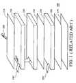
- FIG. 1is a structural diagram of a conventional display device with a digitizer.
- the display device 200comprises a top glass cover 210 , liquid crystal display (LCD) panel 220 , a backlighting module 230 , a reflector 240 , digitizer sensor board 250 , a shield film 260 , a back frame 270 and a position pointer 280 .
- the top glass cover 210 , the LCD panel 220 , the backlighting module 230 , the reflector 240 , the digitizer sensor board 250 , the shield film 260 and the back frame 270are assembled as a laminated construction.
- FIG. 2is a block diagram of a conventional display system with a digitizer.
- display system 100comprises LCD module 220 and digitizer module 250 .
- the LCD module 220 and the digitizer module 250are coupled to the host system 130 via corresponding interfaces 112 and 122 respectively.
- the digitizer module 250requires an oscillator 124 disposed in the microcontroller 126 to generate scan timing signals (SS) for the selection circuit 128 , thereby performing scan operation of sensor array 129 .
- SSscan timing signals
- the inventionis directed to provide a display device that integrates a digitizer sensor board on a LCD module so as to lower thickness and weight.
- a LCD moduledisplays image
- a digitizer sensor board integrated on the surface of the substrate of the LCD modulesenses position of a position pointer or finger contact on a surface.
- the inventiondiscloses an embodiment of a display system, in which the disclosed display device displays images and senses position of a position pointer or finger contact on a surface, and with a shield film laminate on the display system to screen external noise.
- the inventiondiscloses an embodiment of an electronic device, in which the disclosed display system displays images and senses position of a position pointer or finger contact on a surface, and a DC/DC converter is operatively coupled to the display system, powering the display system to display images and sense position of a position pointer or finger contact on a surface.
- the inventiondiscloses an embodiment of a fabrication method of a display device, in which a digitizer sensor board is formed on a glass substrate to serve as an upper substrate of a display device.
- a thin film transistor (TFT) array substrateis formed on lower substrate of the display device. The upper substrate and the lower substrate of the display device are assembled.
- TFTthin film transistor
- the inventiondiscloses an embodiment of another fabrication method of a display device, in which a digitizer sensor board is formed on a glass substrate.
- a thin film transistor (TFT) arrayis formed on the digitizer sensor board, such that the TFT array and the digitizer sensor board on the glass substrate serve as a lower substrate of a LCD module.
- An upper substrate of the LCD moduleis formed and the upper substrate and the lower substrate of the LCD module are assembled.
- FIG. 1is a structural diagram of a conventional display device with digitizer sensor board
- FIG. 2is a block diagram of a conventional display system with a digitizer
- FIG. 3Ashows a first embodiment of a display device
- FIG. 3Bshows a second embodiment of a display device
- FIG. 4is a block diagram of a display device according to the invention.
- FIG. 5is a block diagram of an embodiment of a display system
- FIG. 6shows an embodiment of a timing controller
- FIG. 7schematically shows an electronic device incorporating a display system in accordance with embodiments of the present invention.
- FIG. 3Ashows a first embodiment of a display device.
- the display device 400 Acomprises a top glass cover 410 , a display panel 420 , a backlight module 430 , a reflector 440 , a shield film 460 and a back frame 470 .
- the top glass cover 410 , the backlight module 430 , the reflector 440 , the shield film 460 and the back frame 470are laminated with the display panel 420 in the display device 400 A.
- the LCD module 428is not limited to LCD.
- the display panel 420comprises a LCD display module 428 and a digitizer sensor film 453 integrated on a surface of a glass substrate 452 of the LCD module 428 .
- the LCD module 428comprises an upper substrate 422 , a lower substrate 424 , and a liquid crystal layer 455 , in which the upper substrate 422 comprises a color filter layer 454 , a digitizer sensor board 426 , and a polarizer 450 and the lower substrate 424 comprises a thin film transistor (TFT) array 456 , a glass substrate 457 and a polarizer 458 .
- the color filter layer 454comprises a black matrix (BM) and a plurality of color coated films (CCF) formed therein, the black matrix BM resulting in a non-transparent area in the LCD module 428 .
- the LCD module 428also can be an organic light-emitting diode (OLED) display module or a field emission display (FED) module, although it is to be understood that the invention is not limited thereto.
- OLEDorganic light-emitting diode
- FEDfield emission display
- the backlight module 430 , the reflector 440 or the color filter 454can be omitted.
- the digitizer sensor board 426comprises a glass substrate 452 and a digitizer sensor film 453 formed thereon, with the digitizer sensor board 426 integrated with the color filter layer 454 of the LCD module 428 .
- the digitizer sensor board 426can be a capacitive digitizer sensor board, a resistive digitizer sensor board, an infrared digitizer sensor board, an acoustic wave digitizer sensor board, a piezoelectric force digitizer sensor board, an electrostatic digitizer sensor board or a sonic pulse digitizer sensor board.
- the digitizer sensor film 453can comprise a sensor array, metal coils, metal grids or conductor wires formed on the glass substrate 452 , in which in the sensor array, metal coils, metal grids or conductor are formed in the non-transparent area, thereby avoiding decrease in aperture ratio of the display panel.
- the sensor array, metal coils, metal grids or conductive wirescan be printed on the bottom surface of the glass substrate 452 by screen-printing, ink-jet printing or deposition.
- conductive metal pastes or inkssuch as Ag or Cu based formulations, can be used for screen-printing or ink-jet printing.
- FIG. 3Bshows a second embodiment of a display device.
- the display device 400 Bcomprises a top glass cover 410 , a display panel 420 , a backlight module 430 , a reflector 440 , a shield film 460 and a back frame 470 .
- the digital sensor board 426is integrated on the lower substrate of the LCD module 428 .
- the LCD module 428comprises an upper substrate 422 with a color filter layer 454 and a glass substrate 442 , a lower substrate 424 , and a liquid crystal layer 455 formed between the upper substrate and the lower substrate.
- the lower substrate 424comprises a thin film transistor (TFT) array 456 , a SiO 2 layer 457 and a polarizer 458 .
- the LCD module 428can also be an organic light-emitting diode (OLED) display module or a field emission display (FED) module, although it is to be understood that the invention is not limited thereto.
- OLEDorganic light-emitting diode
- FEDfield emission display
- the backlight module 430 , the reflector 440 or the color filter layer 454can be omitted.
- the digitizer sensor board 426comprises a glass substrate 452 and a digitizer sensor film 453 formed thereon.
- the digitizer sensor board 426is integrated on the lower substrate of LCD module 428 .
- the present inventionalso discloses a fabrication method for a display panel 420 .
- a digitizer sensor filmis formed on a glass substrate to serve as an upper substrate of a display panel.
- the digitizer sensor film 453can be formed on the glass substrate 452 and the color filter 454 is then formed on the digitizer sensor film 453 , as shown in FIG. 3A .
- a polarizer 458is formed on the glass substrate 452 , and a dielectric layer is formed between the color filter 454 and the digitizer sensor film 453 if needed.
- the digitizer sensor board 426comprises the digitizer sensor film 453 and the glass substrate 452 . Namely, the digitizer sensor board 426 is integrated on the upper substrate of the LCD module 428 .
- a thin film transistor (TFT) array substrateis formed to serve as a lower substrate of the display panel.
- the TFT array 456is formed on the glass substrate 457 to serve as a lower substrate 424 of the display panel 428 , in which a polarizer 458 is formed on the glass substrate 457 if needed.
- the upper substrate and the lower substrate of the LCD module 428are assembled into a display panel 420 .
- the LCD module 428can also be an organic light-emitting diode (OLED) display module or a field emission display (FED) module, although it is to be understood that the invention is not limited thereto.
- OLEDorganic light-emitting diode
- FEDfield emission display
- Liquid crystal materialis injected between the upper substrate and the lower substrate to form a liquid crystal layer 455 after the upper substrate and the lower substrate are assembled.
- the inventionalso discloses another fabrication method for a display panel.
- a digitizer sensor boardis formed on a glass substrate and a TFT array 456 is formed on the digitizer sensor board.
- the digitizer sensor film 453can be formed on the glass substrate 452
- a SiO 2 layer 457can be formed on the digitizer sensor film 453
- a thin film transistor (TFT) array 456can be formed on the SiO 2 layer 457 , as shown in FIG. 3B , in which a polarizer 458 is formed on the glass substrate 452 if needed.
- the digitizer sensor board 426 , the SiO 2 layer 457 and the TFT array 456serve as the lower substrate of the display panel 428 . Namely, the digitizer sensor board 426 is integrated on the lower substrate of the display panel 420 .
- An upper substrate of the LCD module 428is formed.
- the color filter 454 laminated with the polarizer 451can serve as the upper substrate of the display panel, as shown in FIG. 3B .
- the upper substrate and the lower substrate of the LCD module 428are assembled to a display panel 420 .
- the LCD module 428can be a liquid crystal display (LCD) module, an organic light-emitting diode (OLED) display module or a field emission display (FED) module, although it is to be understood that the invention is not limited thereto.
- LCDliquid crystal display
- OLEDorganic light-emitting diode
- FEDfield emission display
- liquid crystal materialis injected between the upper substrate and the lower substrate to from a liquid crystal layer 455 after the upper substrate and the lower substrate are assembled.
- FIG. 4shows an embodiment of a display device.
- the display device 400 Ccomprises a top glass cover 410 , a display panel 420 , a backlighting module 430 , a reflector 440 , a shield board 460 and a back frame 470 .
- the display panel 420is coupled to an external host system via a single interface 310 , such as a flexible printed circuit board (FPC).
- the display panel 420comprises a display module and a digitizer sensor board integrated in the display module.
- a control unit 482is mounted on the flexible printed circuit board to drive the display module and generate a scan timing signal SS to the digitizer sensor board according to an image signal from the host system via the interface.
- the display panel 420executes a scan operation to generate position data in response to the scan timing signal, the control unit 482 determines the corresponding coordinate data of the position pointer 480 according to the position data for output to the host system.
- the control unit 482can also, for example, be a chip on glass of the LCD module 428 .
- the LCD module 428can also be a liquid crystal display (LCD) module, an organic light-emitting diode (OLED) module, or a field emission display (FED) module, but it is to be understood that the invention is not limited thereto.
- LCDliquid crystal display
- OLEDorganic light-emitting diode
- FEDfield emission display
- the digitizer sensor board 426 in the display panel 420can be a capacitive sensing digitizer board, a resistive sensing digitizer board, an infrared sensing digitizer board, an acoustic wave sensing digitizer board, or a piezoelectric force sensing digitizer board, an electrostatic sensing digitizer board, or a sonic pulse sensing digitizer board.
- the display system of the embodiment of the inventionrequires only a display panel integrated with a display module and a digitizer sensor board, thickness and weight are less than a conventional display system with separate components.
- FIG. 5is a block diagram of an embodiment of a display system.
- the display system 400 Dcomprises an interface 310 , the control unit 482 , the described digitizer module 426 and the described LCD module 428 .
- the interface 310is coupled between the host system 600 and the control unit 482 , to exchange data with the host system 600 .
- the control unit 482is coupled to the interface 310 , the LCD module 428 and the digitizer module 426 .
- the control unit 482drives the LCD module 428 and generates a scan timing signal (SS) to the digitizer module 426 according to an image signal (IS) from the host system 600 via the interface 310 .
- the control unit 482comprises a timing controller 322 , an analog-to-digital converter 324 , a voltage adjustment circuit 326 and a digital-to-analog converter (DAC) 328 .
- the control unit 482also receives bus control signals (BCS) from the host system 600 via the interface 310 , controlling the operations of the ADC 324 , DAC 328 and the selection circuit 346 .
- BCSbus control signals
- the timing controller 322is coupled to the interface 310 , the LCD module 428 and the digitizer module 426 , generating a driving signal by the DAC 328 according to the image signal (IS) from the host system 600 .
- the image signal (IS) from the host systemcomprises image data (ID), a clock signal (CLKS) and common voltage Vcom, in which the clock signal CLKS includes a vertical scan signal Vs, a horizontal scan signal Hs, a data enable signal DE and a system clock CLK.
- the timing controller 322according to the clock signal CLKS of the image signal, provides reference timing signals comprising a vertical clock output CKV, a horizontal clock output CKH, a horizontal enable output ENBH, a vertical enable output ENBV, a horizontal scan direction CSH and a vertical scan direction CSV, for the LCD module 428 .
- the reference timing signal RTS and the image data IDserve as the driving signal and are output to the DAC 328 for conversion to analog signals driving the LCD module 428 .
- the voltage adjustment circuit 326is coupled to the timing controller 322 and the LCD module 428 , adjusting the voltage level of the analog signal driving the LCD module 428 according to the common voltage Vcom.
- timing controller 322generates the scan timing signal SS to the digitizer module 426 according to the image signal (IS) from the host system 600 . Because the frequency of scan timing signal (SS) required in the digitizer module 426 is between about 100 KHz and 300 KHz and the frequency of the clock signal CLKS in the image signal IS from the host system is typically between 5 MHz and 6 MHz, the embodiment down-converts the clock signal CLKS in the image signal from the host system to obtain a scan timing signal SS with a suitable frequency without utilizing an oscillator as a conventional digitizer board.
- the digitizer module 426 and the LCD 428are coupled to the host system 600 via a single interface.
- timing controller 322comprises a frequency divider 329 to convert the clock signal CLKS of the image signal IS to the scan timing signal SS at a frequency suitable for the digitizer module 426 .
- the LCD module 428is coupled to the control unit 482 to display images according to the analog signals from the DAC 328 .
- the LCD module 428can also be an organic light-emitting diode (OLED) display module, or a field emission display (FED) module.
- OLEDorganic light-emitting diode
- FEDfield emission display
- the digitizer module 426is typically used for cursor control applications, such as selection of displayed icons and menu items, creating or tracing drawings or blueprints, or for character or handwriting recognition.
- the digitizer module 426is coupled to the host system 600 via the interface 310 and executes a scan operation to generate position data PD in response to the scan timing signal SS.
- the digitizer module 426comprises a digitizer sensor array 342 , a selection circuit 346 , and an amplifier 348 .
- the digitizer sensor array 342 , the selection circuit 346 and the amplifier 348are formed on the flexible digitizer sensor film 442 shown in FIG. 3 .
- the selection circuit 346 and the amplifier 348can be integrated to the control unit 482 (not shown).
- the digitizer module 426can be an electromagnetic sensing digitizer board, in which electromagnetic signals are transmitted from the position pointer 480 and sensed by the sensor array 342 .
- the digitizer sensor array 342for example, comprises metal coil grids in both X and Y orientations, sensing the position of the position pointer.
- the position pointertransmits signals to the digitizer sensor array 342 , and the selection circuit 346 scans the coils in the sensor array 342 according to the scan timing signal SS from the control unit 482 , such that signals induced in the digitizer sensor array 342 are sent to the amplifier 348 , and the amplifier 348 amplifies the induced signals in the digitizer sensor array 342 .
- the amplified signals from the amplifier 348are output to the ADC 324 and converted to position data PD to and then to the timing controller 322 .
- the timing controller 322receives the position data PD relative to the position pointer 344 and determines the corresponding coordinate data CD of the digitizer sensor array 342 accordingly.
- the corresponding coordinate data CD of the digitizer sensor array 342is then output to the host system 600 via the interface 310 .
- the control unit 482can be a single chip integrated by the timing controller 322 , the ADC 324 , the voltage adjustment circuit 326 , and the DAC 328 .
- the control unit 320can be mounted directly on the display module 428 by chip on glass (SOG) process or mounted on a flexible printed circuit board (FPC) of the display module 428 .
- FIG. 6shows an embodiment of a timing controller.
- the timing controller 322comprises a processing device 311 , a frequency divider (FD) 329 , a timing generator 332 , a data latch 333 , a register 334 , and a receiving and decoding device 335 , and receives the image signal IS and bus control signal BCS from the host system 600 via the interface 310 .
- FDfrequency divider
- the processing device 331is coupled to the ADC 324 to receive the position data PD and calculate the corresponding coordinate data CD for output to the host system 600 via the interface 310 .
- the host system 600receives the coordinate data DC and converts to image signal to display on the display module.
- the frequency divider 329converts the clock signal CLKS of the image signal to the scan timing signal SS with a suitable frequency, such as 100 KHz ⁇ 300 KHz, for the digitizer sensor board 426 .
- the timing generator 332also receives the clock signal CLKS to provide reference timing signals RTS for the display module 322 .
- the image data ID in the image signal from the host system 600is temporarily stored by the data latch 333 and the register 334 and output to the DAC 328 to drive the display module 428 .
- the receiving and decoding device 335receives the bus control signal BCS from the host system 600 to generate control data controlling operations of the DAC 328 , the ADC 324 and the selection circuit 346 .
- the inventioncan use a single interface and integrate microprocessor 126 and the ADC 125 for digitizer sensor board and timing controller 127 , voltage adjustment circuit 132 , the DAC 131 for the LCD module shown in FIG. 1 into single control unit, such that cost, thickness and weight of the display system are be reduced.
- FIG. 7schematically shows an electronic device 500 deploying the disclosed display systems.
- the display device 400 A/ 400 B/ 400 C/ 400 Dcan be a liquid crystal display system, an organic light-emitting diode (OLED) display system, or a field emission display (FED) system, although it is to be understood that the invention is not limited thereto.
- the electronic device 500may be a portable device such as a PDA, notebook computer, tablet computer, cellular phone, or a display monitor device, etc.
- the electronic device 500includes a housing 510 , the display system 400 A/ 400 B/ 400 C/ 400 D shown in FIG. 4 , a DC/DC converter 520 , etc.
- the DC/DC converter 520is operatively coupled to the display system 400 A/ 400 B/ 400 C/ 400 D and provides an output voltage powering the display system 400 A/ 400 B/ 400 C/ 400 D to display images.
Landscapes
- Engineering & Computer Science (AREA)
- Physics & Mathematics (AREA)
- General Engineering & Computer Science (AREA)
- Theoretical Computer Science (AREA)
- General Physics & Mathematics (AREA)
- Human Computer Interaction (AREA)
- Nonlinear Science (AREA)
- Crystallography & Structural Chemistry (AREA)
- Chemical & Material Sciences (AREA)
- Mathematical Physics (AREA)
- Optics & Photonics (AREA)
- Liquid Crystal (AREA)
- Devices For Indicating Variable Information By Combining Individual Elements (AREA)
- Control Of Indicators Other Than Cathode Ray Tubes (AREA)
- Position Input By Displaying (AREA)
- Electroluminescent Light Sources (AREA)
Abstract
Description
Claims (29)
Priority Applications (6)
| Application Number | Priority Date | Filing Date | Title |
|---|---|---|---|
| US11/311,986US7924269B2 (en) | 2005-01-04 | 2005-12-20 | Display devices and methods forming the same |
| KR1020060068756AKR20070012277A (en) | 2005-07-21 | 2006-07-21 | The process of integrating the digitizer input device into the display |
| TW095126704ATW200710497A (en) | 2005-07-21 | 2006-07-21 | Process of integrating a digitizer input devices in a display |
| US11/490,835US7852324B2 (en) | 2005-07-21 | 2006-07-21 | Process of integrating a digitizer input device in a display |
| JP2006199501AJP2007048279A (en) | 2005-07-21 | 2006-07-21 | Process of integrating digitizer input device in display |
| EP06117673AEP1746485A2 (en) | 2005-07-21 | 2006-07-21 | Process of integrating a digitizer input device in a display |
Applications Claiming Priority (2)
| Application Number | Priority Date | Filing Date | Title |
|---|---|---|---|
| US64128505P | 2005-01-04 | 2005-01-04 | |
| US11/311,986US7924269B2 (en) | 2005-01-04 | 2005-12-20 | Display devices and methods forming the same |
Related Child Applications (1)
| Application Number | Title | Priority Date | Filing Date |
|---|---|---|---|
| US11/490,835Continuation-In-PartUS7852324B2 (en) | 2005-07-21 | 2006-07-21 | Process of integrating a digitizer input device in a display |
Publications (2)
| Publication Number | Publication Date |
|---|---|
| US20060146033A1 US20060146033A1 (en) | 2006-07-06 |
| US7924269B2true US7924269B2 (en) | 2011-04-12 |
Family
ID=36797052
Family Applications (1)
| Application Number | Title | Priority Date | Filing Date |
|---|---|---|---|
| US11/311,986Active2030-01-22US7924269B2 (en) | 2005-01-04 | 2005-12-20 | Display devices and methods forming the same |
Country Status (4)
| Country | Link |
|---|---|
| US (1) | US7924269B2 (en) |
| JP (1) | JP4660639B2 (en) |
| CN (2) | CN101393338A (en) |
| TW (1) | TWI305623B (en) |
Cited By (6)
| Publication number | Priority date | Publication date | Assignee | Title |
|---|---|---|---|---|
| US20090195516A1 (en)* | 2008-02-05 | 2009-08-06 | Au Optronics Corp. | Sensing Structure of a Display |
| US20110148859A1 (en)* | 2009-12-18 | 2011-06-23 | Au Optronics Corp. | Method of determining pointing object position for three-dimensional interactive system |
| US8427622B2 (en) | 2008-12-01 | 2013-04-23 | Hannstar Display Corp. | Liquid crystal display panel having a touch function |
| US9201542B2 (en) | 2012-01-19 | 2015-12-01 | E Ink Holdings Inc. | Light sensitive display apparatus and operating method thereof |
| US9459722B2 (en) | 2014-01-28 | 2016-10-04 | Samsung Display Co., Ltd. | Display apparatus and method of manufacturing the same |
| RU2710515C2 (en)* | 2016-09-14 | 2019-12-26 | Бейджин Сяоми Мобайл Софтвеа Ко., Лтд. | Display device and electronic device |
Families Citing this family (84)
| Publication number | Priority date | Publication date | Assignee | Title |
|---|---|---|---|---|
| US7663607B2 (en) | 2004-05-06 | 2010-02-16 | Apple Inc. | Multipoint touchscreen |
| US7649525B2 (en)* | 2005-01-04 | 2010-01-19 | Tpo Displays Corp. | Display systems with multifunctional digitizer module board |
| EP1746488A2 (en) | 2005-07-21 | 2007-01-24 | TPO Displays Corp. | Electromagnetic digitizer sensor array structure |
| JP2007048279A (en) | 2005-07-21 | 2007-02-22 | Toppoly Optoelectronics Corp | Process of integrating digitizer input device in display |
| JP5268262B2 (en)* | 2006-02-24 | 2013-08-21 | キヤノン株式会社 | Electroluminescence display device |
| CN102981678B (en) | 2006-06-09 | 2015-07-22 | 苹果公司 | Touch screen liquid crystal display |
| US8259078B2 (en)* | 2006-06-09 | 2012-09-04 | Apple Inc. | Touch screen liquid crystal display |
| US20070283832A1 (en)* | 2006-06-09 | 2007-12-13 | Apple Computer, Inc. | Imprint circuit patterning |
| CN104965621B (en) | 2006-06-09 | 2018-06-12 | 苹果公司 | Touch screen LCD and its operating method |
| JP4567028B2 (en) | 2006-09-26 | 2010-10-20 | エルジー ディスプレイ カンパニー リミテッド | Liquid crystal display device having multi-touch sensing function and driving method thereof |
| US8493330B2 (en) | 2007-01-03 | 2013-07-23 | Apple Inc. | Individual channel phase delay scheme |
| US7812827B2 (en)* | 2007-01-03 | 2010-10-12 | Apple Inc. | Simultaneous sensing arrangement |
| US9710095B2 (en) | 2007-01-05 | 2017-07-18 | Apple Inc. | Touch screen stack-ups |
| GB2459799B (en)* | 2007-01-16 | 2010-03-17 | N trig ltd | System and method for calibration of a capacitive touch digitizer system |
| TWI339806B (en)* | 2007-04-04 | 2011-04-01 | Htc Corp | Electronic device capable of executing commands therein and method for executing commands in the same |
| US8493331B2 (en) | 2007-06-13 | 2013-07-23 | Apple Inc. | Touch detection using multiple simultaneous frequencies |
| CN101118325A (en)* | 2007-08-20 | 2008-02-06 | 深圳市和而泰电子科技有限公司 | Touch screen LCD |
| TWI367437B (en)* | 2007-09-29 | 2012-07-01 | Au Optronics Corp | Touch panel and manufacturing method thereof |
| RU2440599C1 (en)* | 2007-12-20 | 2012-01-20 | Шарп Кабусики Кайся | Display with optical sensors |
| TWI374379B (en) | 2007-12-24 | 2012-10-11 | Wintek Corp | Transparent capacitive touch panel and manufacturing method thereof |
| TWM348999U (en)* | 2008-02-18 | 2009-01-11 | Tpk Touch Solutions Inc | Capacitive touch panel |
| CN101551722B (en)* | 2008-04-01 | 2011-01-12 | 晶宏半导体股份有限公司 | Touch panel structure with signal processing chip |
| TW200945596A (en)* | 2008-04-16 | 2009-11-01 | Mosel Vitelic Inc | A method for making a solar cell with a selective emitter |
| KR20090112118A (en)* | 2008-04-23 | 2009-10-28 | 엘지이노텍 주식회사 | Display |
| US8508495B2 (en) | 2008-07-03 | 2013-08-13 | Apple Inc. | Display with dual-function capacitive elements |
| TWI463354B (en) | 2008-08-13 | 2014-12-01 | Prime View Int Co Ltd | Display panel and touch-sensitive display module |
| US9606663B2 (en) | 2008-09-10 | 2017-03-28 | Apple Inc. | Multiple stimulation phase determination |
| US9348451B2 (en) | 2008-09-10 | 2016-05-24 | Apple Inc. | Channel scan architecture for multiple stimulus multi-touch sensor panels |
| US8592697B2 (en) | 2008-09-10 | 2013-11-26 | Apple Inc. | Single-chip multi-stimulus sensor controller |
| US8482545B2 (en)* | 2008-10-02 | 2013-07-09 | Wacom Co., Ltd. | Combination touch and transducer input system and method |
| KR101033997B1 (en)* | 2008-11-11 | 2011-05-11 | 주식회사 애트랩 | Touch panel and input device having the same |
| US8144295B2 (en) | 2008-11-18 | 2012-03-27 | Apple Inc. | Common bus design for a TFT-LCD display |
| US20100123686A1 (en)* | 2008-11-19 | 2010-05-20 | Sony Ericsson Mobile Communications Ab | Piezoresistive force sensor integrated in a display |
| US8749496B2 (en) | 2008-12-05 | 2014-06-10 | Apple Inc. | Integrated touch panel for a TFT display |
| US7995041B2 (en)* | 2009-02-02 | 2011-08-09 | Apple Inc. | Integrated touch screen |
| US8217913B2 (en) | 2009-02-02 | 2012-07-10 | Apple Inc. | Integrated touch screen |
| TWI414974B (en)* | 2009-06-17 | 2013-11-11 | Novatek Microelectronics Corp | Touch position sensing method and position sensing system of touch panel |
| CN101930134B (en)* | 2009-06-19 | 2013-08-07 | 台均科技(深圳)有限公司 | Electromagnetic induction type liquid crystal panel and its manufacturing method and liquid crystal display |
| JP5252309B2 (en)* | 2009-08-21 | 2013-07-31 | 凸版印刷株式会社 | Manufacturing method of color filter substrate with touch panel electrode |
| TWI419036B (en)* | 2009-10-23 | 2013-12-11 | Au Optronics Corp | Touch display panel and touch sensing unit thereof |
| TW201118456A (en)* | 2009-11-20 | 2011-06-01 | Prime View Int Co Ltd | Touch display module and touch display apparatus comprising the same |
| CN102214053A (en)* | 2010-04-02 | 2011-10-12 | 太瀚科技股份有限公司 | Lightweight full-plane electromagnetic induction tablet |
| CN102214027A (en)* | 2010-04-06 | 2011-10-12 | 元太科技工业股份有限公司 | Display panel |
| KR101799031B1 (en) | 2010-08-09 | 2017-12-21 | 삼성디스플레이 주식회사 | Liquid crystal display including touch sensor layer and method thereof |
| US8804056B2 (en) | 2010-12-22 | 2014-08-12 | Apple Inc. | Integrated touch screens |
| TW201237720A (en)* | 2011-03-11 | 2012-09-16 | Cando Corp | Thin type flexible capacitive touch device |
| CN102693030A (en)* | 2011-03-21 | 2012-09-26 | 奇美电子股份有限公司 | Manufacturing method of touch display panel |
| TWI534664B (en)* | 2011-07-28 | 2016-05-21 | 宸鴻光電科技股份有限公司 | Touch sensitive display |
| KR20130020313A (en)* | 2011-08-19 | 2013-02-27 | 삼성전기주식회사 | Touch sensor and method for manufacturing the same |
| TWI461979B (en)* | 2012-03-19 | 2014-11-21 | Mstar Semiconductor Inc | Control system for touch screen |
| US9395583B2 (en) | 2012-06-06 | 2016-07-19 | Apple Inc. | Column spacer design for a display incorporating a third metal layer |
| JP6055206B2 (en) | 2012-06-08 | 2016-12-27 | 株式会社ジャパンディスプレイ | Liquid crystal display |
| KR101391243B1 (en)* | 2012-07-17 | 2014-05-02 | 삼성디스플레이 주식회사 | display device having touch sensing function |
| CN103576963A (en)* | 2012-08-07 | 2014-02-12 | 英华达(上海)科技有限公司 | Touch display device and case thereof |
| KR102114212B1 (en) | 2012-08-10 | 2020-05-22 | 가부시키가이샤 한도오따이 에네루기 켄큐쇼 | Display device |
| US9000452B2 (en) | 2012-09-28 | 2015-04-07 | Industrial Technology Research Institute | Display with filter structure |
| KR20140045076A (en)* | 2012-10-08 | 2014-04-16 | 삼성전자주식회사 | Method and apparatus for increasing performance of in-cell touch-screen |
| CN103855182A (en)* | 2012-11-28 | 2014-06-11 | 瀚宇彩晶股份有限公司 | Organic light emitting diode touch display panel and electromagnetic touch display device thereof |
| TWI481933B (en)* | 2012-12-28 | 2015-04-21 | Ye Xin Technology Consulting Co Ltd | Touch display device |
| US9336723B2 (en) | 2013-02-13 | 2016-05-10 | Apple Inc. | In-cell touch for LED |
| KR102048941B1 (en)* | 2013-04-12 | 2020-01-09 | 삼성디스플레이 주식회사 | Flexible substrate and manufacturing method thereof, organic light emitting diode display |
| CN103257744A (en)* | 2013-04-16 | 2013-08-21 | 南昌欧菲光显示技术有限公司 | Optical filter module and touch display screen with same |
| KR102046296B1 (en)* | 2013-04-26 | 2019-11-19 | 엘지디스플레이 주식회사 | Touch-Type Organic Light-Emitting Diode Display Device |
| CN103927069B (en)* | 2013-05-08 | 2017-02-08 | 上海中航光电子有限公司 | Inductance touch screen and embedded inductance touch screen |
| KR101487463B1 (en)* | 2013-07-03 | 2015-01-28 | 주식회사 더한 | Tablet detecting induced electromagnetic field and capacitive touch |
| KR101681305B1 (en)* | 2014-08-01 | 2016-12-02 | 주식회사 하이딥 | Touch input device |
| KR101452302B1 (en) | 2013-07-29 | 2014-10-22 | 주식회사 하이딥 | Touch sensor panel |
| KR20160011196A (en) | 2013-09-20 | 2016-01-29 | 애플 인크. | Pressure-sensing stages for lamination systems |
| KR101712346B1 (en) | 2014-09-19 | 2017-03-22 | 주식회사 하이딥 | Touch input device |
| CN116560524B (en) | 2013-12-13 | 2024-10-01 | 苹果公司 | Integrated touch and display architecture for self-capacitance touch sensor |
| WO2015160377A1 (en) | 2014-04-16 | 2015-10-22 | Wrostix Technologies Llc | Structure for pixelated self-capacitance |
| US10133382B2 (en) | 2014-05-16 | 2018-11-20 | Apple Inc. | Structure for integrated touch screen |
| US9367188B2 (en) | 2014-05-23 | 2016-06-14 | Apple Inc. | RC matching in a touch screen |
| WO2015183334A1 (en) | 2014-05-28 | 2015-12-03 | Pylemta Management Llc | Narrow border touch screen |
| JP6527343B2 (en) | 2014-08-01 | 2019-06-05 | 株式会社 ハイディープHiDeep Inc. | Touch input device |
| US9671913B2 (en) | 2015-05-11 | 2017-06-06 | Microsoft Technology Licensing, Llc | Capacitive display device |
| CN106293170A (en)* | 2015-05-18 | 2017-01-04 | 中兴通讯股份有限公司 | Display floater, electronic equipment and be applied to the touch control inducing method of electronic equipment |
| TW201736814A (en)* | 2016-04-12 | 2017-10-16 | 原相科技股份有限公司 | Pressure measuring method and pressure measuring apparatus |
| CN205900543U (en)* | 2016-05-18 | 2017-01-18 | 武汉华星光电技术有限公司 | OLED (Organic light emitting diode) display panel |
| CN106129091A (en)* | 2016-07-22 | 2016-11-16 | 京东方科技集团股份有限公司 | A kind of electroluminescence display panel and el display device |
| TWI653570B (en) | 2018-03-15 | 2019-03-11 | 宏碁股份有限公司 | Electromagnetic touch-sensing device and method of operating the same |
| CN109085949B (en)* | 2018-07-27 | 2021-08-03 | 上海天马微电子有限公司 | Array substrate and display device |
| US20200192542A1 (en)* | 2018-12-12 | 2020-06-18 | Novatek Microelectronics Corp. | Display device with integrated antenna and method thereof |
| CN114341970B (en)* | 2019-09-06 | 2025-04-15 | 布瑞威利私人有限公司 | Display Components |
Citations (19)
| Publication number | Priority date | Publication date | Assignee | Title |
|---|---|---|---|---|
| JPH0713710A (en) | 1993-06-28 | 1995-01-17 | Canon Inc | Printing system |
| JPH07200177A (en) | 1993-12-28 | 1995-08-04 | Mitsumi Electric Co Ltd | Information processor |
| JPH0980467A (en) | 1995-09-14 | 1997-03-28 | Toshiba Corp | Active matrix display device with pen input position detection function |
| US5644653A (en)* | 1993-05-07 | 1997-07-01 | Canon Kabushiki Kaisha | Information processing apparatus and control method thereof having user character recognition |
| US5670755A (en) | 1994-04-21 | 1997-09-23 | Samsung Display Devices Co., Ltd. | Information input apparatus having functions of both touch panel and digitizer, and driving method thereof |
| JPH09258893A (en) | 1996-03-25 | 1997-10-03 | Toshiba Corp | Coordinate input device and input display device including the same |
| US5821916A (en)* | 1992-08-13 | 1998-10-13 | Calcomp, Inc. | Digitizer cursor velocity offset error correction system |
| JPH11271712A (en) | 1998-03-20 | 1999-10-08 | Toshiba Corp | Liquid crystal display device and position detection device |
| CN1286424A (en) | 1999-08-31 | 2001-03-07 | 大赛璐化学工业株式会社 | Touch screen and display device using said touch screen |
| JP2001183630A (en) | 1999-12-24 | 2001-07-06 | Casio Comput Co Ltd | Display device with coordinates input function |
| US6285417B1 (en) | 1997-10-31 | 2001-09-04 | Lg.Philips Lcd Co., Ltd. | Position sensing liquid crystal display and method for fabricating the same |
| JP2003196023A (en) | 2001-12-27 | 2003-07-11 | Sony Corp | Display device |
| US6661399B1 (en) | 1999-06-21 | 2003-12-09 | Lg.Philips Lcd Co., Ltd. | Liquid crystal display device having a digitizer |
| JP2004215057A (en) | 2003-01-07 | 2004-07-29 | Pac Interactive Technology Inc | Block type information electric appliance system structure |
| CN1534333A (en) | 2003-03-28 | 2004-10-06 | Lg.飞利浦Lcd有限公司 | Liquid crystal display device with electromagnetic type touch screen |
| US20050133279A1 (en) | 2003-12-17 | 2005-06-23 | Microsoft Corporation | Electromagnetic digitizer sensor array |
| US7196695B2 (en)* | 2002-07-30 | 2007-03-27 | Au Optronics Corp. | Flat panel display in which a digitizer is integrated |
| US7292229B2 (en) | 2002-08-29 | 2007-11-06 | N-Trig Ltd. | Transparent digitiser |
| US7298367B2 (en)* | 2003-11-25 | 2007-11-20 | 3M Innovative Properties Company | Light emitting stylus and user input device using same |
Family Cites Families (4)
| Publication number | Priority date | Publication date | Assignee | Title |
|---|---|---|---|---|
| KR100840670B1 (en)* | 2001-12-27 | 2008-06-24 | 엘지디스플레이 주식회사 | Touch panel integrated liquid crystal display panel |
| CN2569259Y (en)* | 2002-09-16 | 2003-08-27 | 台均实业有限公司 | Touch control display with built-in diaphragm antenna array grid electromagnetic induction layer |
| MXPA03009945A (en)* | 2002-11-05 | 2007-04-16 | Lg Electronics Inc | Touch screen mounting assembly for lcd monitor. |
| KR100519371B1 (en)* | 2002-12-24 | 2005-10-07 | 엘지.필립스 엘시디 주식회사 | liquid crystal display device with touch panel |
- 2005
- 2005-12-20USUS11/311,986patent/US7924269B2/enactiveActive
- 2005-12-28JPJP2005377161Apatent/JP4660639B2/ennot_activeExpired - Fee Related
- 2005-12-30TWTW094147615Apatent/TWI305623B/ennot_activeIP Right Cessation
- 2006
- 2006-01-04CNCNA2008101670166Apatent/CN101393338A/enactivePending
- 2006-01-04CNCNB2006100036013Apatent/CN100516988C/ennot_activeExpired - Fee Related
Patent Citations (20)
| Publication number | Priority date | Publication date | Assignee | Title |
|---|---|---|---|---|
| US5821916A (en)* | 1992-08-13 | 1998-10-13 | Calcomp, Inc. | Digitizer cursor velocity offset error correction system |
| US5644653A (en)* | 1993-05-07 | 1997-07-01 | Canon Kabushiki Kaisha | Information processing apparatus and control method thereof having user character recognition |
| JPH0713710A (en) | 1993-06-28 | 1995-01-17 | Canon Inc | Printing system |
| JPH07200177A (en) | 1993-12-28 | 1995-08-04 | Mitsumi Electric Co Ltd | Information processor |
| US5670755A (en) | 1994-04-21 | 1997-09-23 | Samsung Display Devices Co., Ltd. | Information input apparatus having functions of both touch panel and digitizer, and driving method thereof |
| JPH0980467A (en) | 1995-09-14 | 1997-03-28 | Toshiba Corp | Active matrix display device with pen input position detection function |
| JPH09258893A (en) | 1996-03-25 | 1997-10-03 | Toshiba Corp | Coordinate input device and input display device including the same |
| US6285417B1 (en) | 1997-10-31 | 2001-09-04 | Lg.Philips Lcd Co., Ltd. | Position sensing liquid crystal display and method for fabricating the same |
| US6388729B2 (en)* | 1997-10-31 | 2002-05-14 | Lg. Philips Lcd Co., Ltd. | Position sensing liquid crystal display and method for fabricating the same |
| JPH11271712A (en) | 1998-03-20 | 1999-10-08 | Toshiba Corp | Liquid crystal display device and position detection device |
| US6661399B1 (en) | 1999-06-21 | 2003-12-09 | Lg.Philips Lcd Co., Ltd. | Liquid crystal display device having a digitizer |
| CN1286424A (en) | 1999-08-31 | 2001-03-07 | 大赛璐化学工业株式会社 | Touch screen and display device using said touch screen |
| JP2001183630A (en) | 1999-12-24 | 2001-07-06 | Casio Comput Co Ltd | Display device with coordinates input function |
| JP2003196023A (en) | 2001-12-27 | 2003-07-11 | Sony Corp | Display device |
| US7196695B2 (en)* | 2002-07-30 | 2007-03-27 | Au Optronics Corp. | Flat panel display in which a digitizer is integrated |
| US7292229B2 (en) | 2002-08-29 | 2007-11-06 | N-Trig Ltd. | Transparent digitiser |
| JP2004215057A (en) | 2003-01-07 | 2004-07-29 | Pac Interactive Technology Inc | Block type information electric appliance system structure |
| CN1534333A (en) | 2003-03-28 | 2004-10-06 | Lg.飞利浦Lcd有限公司 | Liquid crystal display device with electromagnetic type touch screen |
| US7298367B2 (en)* | 2003-11-25 | 2007-11-20 | 3M Innovative Properties Company | Light emitting stylus and user input device using same |
| US20050133279A1 (en) | 2003-12-17 | 2005-06-23 | Microsoft Corporation | Electromagnetic digitizer sensor array |
Cited By (7)
| Publication number | Priority date | Publication date | Assignee | Title |
|---|---|---|---|---|
| US20090195516A1 (en)* | 2008-02-05 | 2009-08-06 | Au Optronics Corp. | Sensing Structure of a Display |
| US8427622B2 (en) | 2008-12-01 | 2013-04-23 | Hannstar Display Corp. | Liquid crystal display panel having a touch function |
| US20110148859A1 (en)* | 2009-12-18 | 2011-06-23 | Au Optronics Corp. | Method of determining pointing object position for three-dimensional interactive system |
| US8531458B2 (en)* | 2009-12-18 | 2013-09-10 | Au Optronics Corp. | Method of determining pointing object position for three-dimensional interactive system |
| US9201542B2 (en) | 2012-01-19 | 2015-12-01 | E Ink Holdings Inc. | Light sensitive display apparatus and operating method thereof |
| US9459722B2 (en) | 2014-01-28 | 2016-10-04 | Samsung Display Co., Ltd. | Display apparatus and method of manufacturing the same |
| RU2710515C2 (en)* | 2016-09-14 | 2019-12-26 | Бейджин Сяоми Мобайл Софтвеа Ко., Лтд. | Display device and electronic device |
Also Published As
| Publication number | Publication date |
|---|---|
| CN100516988C (en) | 2009-07-22 |
| JP4660639B2 (en) | 2011-03-30 |
| TWI305623B (en) | 2009-01-21 |
| CN1800928A (en) | 2006-07-12 |
| US20060146033A1 (en) | 2006-07-06 |
| CN101393338A (en) | 2009-03-25 |
| JP2006189859A (en) | 2006-07-20 |
Similar Documents
| Publication | Publication Date | Title |
|---|---|---|
| US7924269B2 (en) | Display devices and methods forming the same | |
| US7649525B2 (en) | Display systems with multifunctional digitizer module board | |
| US7552861B2 (en) | Display system | |
| JP5794810B2 (en) | Method and apparatus for compensating parasitic capacitance of touch panel | |
| JP5827807B2 (en) | Touch panel noise compensation method and apparatus | |
| CN102446026B (en) | There is the display device of touch panel | |
| EP2527962B1 (en) | Integrated digitizer display | |
| US9064772B2 (en) | Touch screen system having dual touch sensing function | |
| KR20190014926A (en) | Display device | |
| CN107025011B (en) | Display panel with built-in touch screen and touch display device including same | |
| KR20110051048A (en) | Touch screen input device and manufacturing method | |
| WO2020224309A1 (en) | Electronic apparatus having fingerprint sensing function | |
| US9361847B2 (en) | Display device and driving method thereof | |
| US20070216663A1 (en) | Method of producing a touch panel | |
| KR200234683Y1 (en) | Plat Panel Display with Input Device | |
| KR200455938Y1 (en) | Integrated board of graphic user interface | |
| KR20010094774A (en) | Plat Panel Display with Input Device |
Legal Events
| Date | Code | Title | Description |
|---|---|---|---|
| AS | Assignment | Owner name:TOPPOLY OPTOELECTRONICS CORP., TAIWAN Free format text:ASSIGNMENT OF ASSIGNORS INTEREST;ASSIGNORS:CHEN, DIN-GUO;LEE, YING-CHIH;HO, SHYUAN-JENG;REEL/FRAME:017355/0043 Effective date:20051213 | |
| AS | Assignment | Owner name:TPO DISPLAYS CORP., TAIWAN Free format text:CHANGE OF NAME;ASSIGNOR:TOPPOLY OPTOELECTRONICS CORP.;REEL/FRAME:025584/0544 Effective date:20060605 | |
| AS | Assignment | Owner name:TPO DISPLAYS CORP., TAIWAN Free format text:CHANGE OF NAME;ASSIGNOR:TOPPOLY OPTOELECTRONICS CORP.;REEL/FRAME:025681/0254 Effective date:20060605 | |
| AS | Assignment | Owner name:CHIMEI INNOLUX CORPORATION, TAIWAN Free format text:MERGER;ASSIGNOR:TPO DISPLAYS CORP.;REEL/FRAME:025919/0338 Effective date:20100318 Owner name:CHIMEI INNOLUX CORPORATION, TAIWAN Free format text:MERGER;ASSIGNOR:TPO DISPLAYS CORP.;REEL/FRAME:025918/0759 Effective date:20100318 | |
| STCF | Information on status: patent grant | Free format text:PATENTED CASE | |
| AS | Assignment | Owner name:INNOLUX CORPORATION, TAIWAN Free format text:CHANGE OF NAME;ASSIGNOR:CHIMEI INNOLUX CORPORATION;REEL/FRAME:032621/0718 Effective date:20121219 | |
| FPAY | Fee payment | Year of fee payment:4 | |
| MAFP | Maintenance fee payment | Free format text:PAYMENT OF MAINTENANCE FEE, 8TH YEAR, LARGE ENTITY (ORIGINAL EVENT CODE: M1552); ENTITY STATUS OF PATENT OWNER: LARGE ENTITY Year of fee payment:8 | |
| MAFP | Maintenance fee payment | Free format text:PAYMENT OF MAINTENANCE FEE, 12TH YEAR, LARGE ENTITY (ORIGINAL EVENT CODE: M1553); ENTITY STATUS OF PATENT OWNER: LARGE ENTITY Year of fee payment:12 | |
| AS | Assignment | Owner name:RED OAK INNOVATIONS LIMITED, IRELAND Free format text:ASSIGNMENT OF ASSIGNORS INTEREST;ASSIGNOR:INNOLUX CORPORATION;REEL/FRAME:069206/0903 Effective date:20240925 |