US7922474B2 - Imprint lithography - Google Patents
Imprint lithographyDownload PDFInfo
- Publication number
- US7922474B2 US7922474B2US11/155,941US15594105AUS7922474B2US 7922474 B2US7922474 B2US 7922474B2US 15594105 AUS15594105 AUS 15594105AUS 7922474 B2US7922474 B2US 7922474B2
- Authority
- US
- United States
- Prior art keywords
- substrate
- template
- force
- imprinting
- compensating
- Prior art date
- Legal status (The legal status is an assumption and is not a legal conclusion. Google has not performed a legal analysis and makes no representation as to the accuracy of the status listed.)
- Expired - Fee Related, expires
Links
Images


Classifications
- G—PHYSICS
- G03—PHOTOGRAPHY; CINEMATOGRAPHY; ANALOGOUS TECHNIQUES USING WAVES OTHER THAN OPTICAL WAVES; ELECTROGRAPHY; HOLOGRAPHY
- G03F—PHOTOMECHANICAL PRODUCTION OF TEXTURED OR PATTERNED SURFACES, e.g. FOR PRINTING, FOR PROCESSING OF SEMICONDUCTOR DEVICES; MATERIALS THEREFOR; ORIGINALS THEREFOR; APPARATUS SPECIALLY ADAPTED THEREFOR
- G03F7/00—Photomechanical, e.g. photolithographic, production of textured or patterned surfaces, e.g. printing surfaces; Materials therefor, e.g. comprising photoresists; Apparatus specially adapted therefor
- G03F7/0002—Lithographic processes using patterning methods other than those involving the exposure to radiation, e.g. by stamping
- B—PERFORMING OPERATIONS; TRANSPORTING
- B82—NANOTECHNOLOGY
- B82Y—SPECIFIC USES OR APPLICATIONS OF NANOSTRUCTURES; MEASUREMENT OR ANALYSIS OF NANOSTRUCTURES; MANUFACTURE OR TREATMENT OF NANOSTRUCTURES
- B82Y10/00—Nanotechnology for information processing, storage or transmission, e.g. quantum computing or single electron logic
- B—PERFORMING OPERATIONS; TRANSPORTING
- B82—NANOTECHNOLOGY
- B82Y—SPECIFIC USES OR APPLICATIONS OF NANOSTRUCTURES; MEASUREMENT OR ANALYSIS OF NANOSTRUCTURES; MANUFACTURE OR TREATMENT OF NANOSTRUCTURES
- B82Y40/00—Manufacture or treatment of nanostructures
- C—CHEMISTRY; METALLURGY
- C23—COATING METALLIC MATERIAL; COATING MATERIAL WITH METALLIC MATERIAL; CHEMICAL SURFACE TREATMENT; DIFFUSION TREATMENT OF METALLIC MATERIAL; COATING BY VACUUM EVAPORATION, BY SPUTTERING, BY ION IMPLANTATION OR BY CHEMICAL VAPOUR DEPOSITION, IN GENERAL; INHIBITING CORROSION OF METALLIC MATERIAL OR INCRUSTATION IN GENERAL
- C23F—NON-MECHANICAL REMOVAL OF METALLIC MATERIAL FROM SURFACE; INHIBITING CORROSION OF METALLIC MATERIAL OR INCRUSTATION IN GENERAL; MULTI-STEP PROCESSES FOR SURFACE TREATMENT OF METALLIC MATERIAL INVOLVING AT LEAST ONE PROCESS PROVIDED FOR IN CLASS C23 AND AT LEAST ONE PROCESS COVERED BY SUBCLASS C21D OR C22F OR CLASS C25
- C23F1/00—Etching metallic material by chemical means
- C23F1/02—Local etching
- Y—GENERAL TAGGING OF NEW TECHNOLOGICAL DEVELOPMENTS; GENERAL TAGGING OF CROSS-SECTIONAL TECHNOLOGIES SPANNING OVER SEVERAL SECTIONS OF THE IPC; TECHNICAL SUBJECTS COVERED BY FORMER USPC CROSS-REFERENCE ART COLLECTIONS [XRACs] AND DIGESTS
- Y10—TECHNICAL SUBJECTS COVERED BY FORMER USPC
- Y10S—TECHNICAL SUBJECTS COVERED BY FORMER USPC CROSS-REFERENCE ART COLLECTIONS [XRACs] AND DIGESTS
- Y10S977/00—Nanotechnology
- Y10S977/84—Manufacture, treatment, or detection of nanostructure
- Y10S977/887—Nanoimprint lithography, i.e. nanostamp
Definitions
- the present inventionrelates to imprint lithography.
- a lithographic apparatusis a machine that applies a desired pattern onto a target portion of a substrate.
- Lithographic apparatusare conventionally used, for example, in the manufacture of integrated circuits (ICs), flat panel displays and other devices involving fine structures.
- An alternative method to printing sub-100 nm featurescomprises transferring a pattern to a substrate by imprinting a pattern into an imprintable medium using a physical mould or template.
- the imprintable mediummay be the substrate or a material coated onto a surface of the substrate.
- the imprintable mediummay be functional or may be used as a “mask” to transfer a pattern to an underlying surface.
- the imprintable mediummay, for instance, be provided as a resist deposited on a substrate, such as a semiconductor material, to which the pattern defined by the template is to be transferred.
- Imprint lithographyis thus essentially a moulding process on a micrometer or nanometer scale in which the topography of a template defines the patterns created on a substrate. Patterns may be layered as with optical lithography processes so that in principle imprint lithography could be used for such applications as integrated circuit manufacture.
- imprint lithographyis limited only by the resolution of the template fabrication process.
- imprint lithographyhas been used to produce features in the sub-50 nm range with significantly improved resolution and line edge roughness compared to that achievable with conventional optical lithography processes.
- imprint processesmay not require the expensive optics, advanced illumination sources or specialized resist materials typically required for optical lithography processes.
- an imprinting methodcomprising applying an imprinting force to a template to cause the template to contact an imprintable medium on a target region of a first surface of a substrate to form an imprint in the medium, during application of the imprinting force, applying a compensating force to a second surface of the substrate which is opposite to the first surface so as to reduce deformation of the substrate caused by the application of the imprinting force, and separating the template from the imprinted medium.
- deformatione.g. bending or compression
- deformation of the substratemay be reduced, minimized, or substantially eliminated, by the application of an appropriate compensatory force provided by, e.g., a suitably arranged compensating member.
- the contact area of the compensating member employed to apply the compensating force to the second surface of the substratemay be greater than, similar to or smaller than the area of the second surface of the substrate.
- the compensating forcemay be applied at any convenient angle to any desirable portion of the second surface of the substrate
- the compensating forceis applied, in an embodiment, to a portion of the second (e.g. bottom) surface of the substrate which is directly opposite to the target region of the first (e.g. top) surface of the substrate.
- the magnitude of the compensating forcemay be reduced or minimized since its trajectory is aligned with that of the imprinting force.
- the target region of the first surface of the substrateis a fraction of the total surface area of the first surface of the substrate, i.e. the target region has a smaller surface area than the total area of the first surface of the substrate.
- the portion of the second surface of the substrate over which the compensating force is applied by the compensating memberis, in an embodiment, a fraction of the total area of the second surface of the substrate.
- the compensating forceis substantially equal to the imprinting force.
- the compensating forcemay be greater than the imprinting force so as to compensate for compression of a part of the target region of the first surface of the substrate.
- the compensating pressure exerted on the second surface of the substrate by virtue of the application of the compensating forcemay be substantially equal to or greater than the imprinting pressure exerted on the imprintable medium due to the application of the imprinting force.
- the substrateis supported on a first surface of a carrier and the compensating force is applied by a compensating member directly contacting a second surface of the carrier which is opposite to the first surface of the carrier.
- the compensating forceis applied using a resilient member.
- the compensating forceis applied using a compensating member selected from a group consisting of a spring, a piezoelectrically actuated member and a red displaceably mounted within a coil capable of carrying an electric current (e.g. a Lorentz motor).
- the imprinting methodmay further comprise providing a volume of this imprintable medium on the target region of the first surface of the substrate.
- an imprinting methodcomprising applying an imprinting force to a template to cause the template to contact an imprintable medium on a target region of the first surface of a substrate, the target region having an area less than the area of the first surface of the substrate, to form an imprint in the medium; during application of the imprinting force, applying a localized compensating force to a second surface of the substrate which is opposite to the first surface of the substrate so as to reduce deformation of the substrate caused by the application of the imprinting force; and separating the template from the imprinted medium.
- the applicationby any suitable means, e.g. mechanical force, fluid pressure, etc.
- an appropriate localized compensating forceto a specific portion of the second surface of the substrate enables the magnitude of the compensating force to be reduced.
- the portion or the second surface of the substrateis directly opposite to the target region of the first surface of the substrate.
- the trajectory of the compensating forcewill be aligned with that of the imprinting force allowing the magnitude of the compensating force to be reduced further. Since the target region of the first surface of the substrate is a fraction of the total surface area of the first surface of the substrate, the portion of the second surface of the substrate over which the localized compensating force is applied by the compensating member is, in an embodiment, a fraction of the total area of the second surface of the substrate.
- the imprinting methodfurther comprises providing a volume of the imprintable medium on the target region of the first surface of the substrate.
- a method for patterning a substratecomprising:
- an imprinting forceto a template to cause the template to contact an imprintable medium on a target region of a first surface of a substrate to form an imprint in the medium, the imprint comprising a pattern feature and an area of reduced thickness;
- the imprinting method described earliermay be incorporated in to a substrate patterning method as defined according to this aspect.
- the methodfurther comprises providing a volume of the imprintable medium on the target region of the first surface of the substrate.
- a method for patterning a substratecomprising:
- an imprinting forceto a template to cause the template to contact an imprintable medium on a target region of a first surface of a substrate, the target region having an area less than the area of the first surface of the substrate, to form an imprint in the medium, the imprint comprising a pattern feature and an area of reduced thickness;
- the methodfurther comprises providing a volume of the imprintable medium on the target region of the first surface of the substrate.
- an imprinting apparatuscomprising:
- a substrate holderconfigured to hold a substrate
- a template holderconfigured to hold a template, the template holder being operable to apply an imprinting force to the template to cause the template to contact an imprintable medium on a target region of a first surface of the substrate to form an imprint in the medium and to cause the template to separate from the imprinted medium;
- a compensating memberoperable to apply a compensating force, during application of the imprinting force, to a second surface of the substrate which is opposite to the first surface so as to reduce deformation of the substrate caused by the application of the imprinting force
- the compensating forcemay be applied an any convenient angle to any desirable portion of the second surface of the substrate, however, in an embodiment, the compensating member is operable to apply the compensating force to a portion of the second surface of the substrate which is directly opposite the first target region of the first surface of the substrate.
- the compensating memberis operable to provide a compensating force which is substantially equal to or greater than the imprinting force. Furthermore, the compensating member may be operable to provide a compensating force which exerts a compensating pressure on the second surface of the substrate which is substantially equal to or greater than the imprinting pressure exerted on the imprintable medium due to the application of the imprinting force by operation of the template holder.
- the substrateis supported on a first surface of a carrier and the compensating member directly contacts a second surface of the carrier which is opposite to the first surface of the carrier.
- the compensating memberis connected to the substrate holder.
- the compensating membermay be a resilient member.
- the compensating memberis selected from a group consisting of a spring, a piezoelectrically actuated member, and a rod displaceably mounted within a coil capable of carrying an electric current (e.g. a Lorentz motor).
- the imprinting apparatusfurther comprises dosing apparatus configured to provide a volume of the imprintable medium on the target region of the first surface of the substrate held on the substrate holder.
- an imprinting apparatuscomprising:
- a substrate holderconfigured to hold a substrate
- a template holderconfigured to hold a template, the template holder being operable to apply an imprinting force to the template to cause the template to contact an imprintable medium on a target region of a first surface of the substrate to form an imprint in the medium, the target region having an area less than the area of the first surface of the substrate, and to cause the template to separate from the imprinted medium;
- a compensating memberoperable to apply a localized compensating force, during application of the imprinting force, to a second surface of the substrate which is opposite to the first surface of the substrate so as to reduce deformation of the substrate caused by the application of the imprinting force.
- the imprinting apparatusfurther comprises a dosing apparatus configured to provide a volume of the imprintable medium on the target region of the first surface of the substrate held on the substrate holder.
- FIG. 1 a - 1 cillustrate examples of soft, hot and UV lithography processes respectively
- FIG. 2illustrates a two step etching process employed when hot and UV imprint lithography is used to pattern a resist layer
- FIG. 3illustrates relative dimensions of template features compared to the thickness of a typical imprintable resist layer deposited on a substrate
- FIG. 4illustrates flexure of a substrate when subjected to a stamping force
- FIG. 5illustrates provision of a counter force in accordance with an embodiment of the present invention.
- FIGS. 6 , 7 and 8illustrate mechanisms for releasing a template.
- FIGS. 1 a to 1 cThere are two principal approaches to imprint lithography which will be termed generally as hot imprint lithography and UV imprint lithography. There is also a third type of “printing” lithography known as soft lithography. Examples of these are illustrated in FIGS. 1 a to 1 c.
- FIG. 1 aschematically depicts the soft lithography process which involves transferring a layer of molecules 11 (typically an ink such as a thiol) from a flexible template 10 (typically fabricated from polydimethylsiloxane (PDMS)) onto a resist layer 13 which is supported upon a substrate 12 and planarization and transfer layer 12 ′.
- the template 10has a pattern of features on its surface, the molecular layer being disposed upon the features.
- the layer of molecules 11stick to the resist.
- the residual layer of resistis etched such that the areas of the resist not covered by the transferred molecular layer are etched down to the substrate.
- the template used in soft lithographymay be easily deformed and may therefore not be suited to high resolution applications, e.g. on a nanometer scale, since the deformation of the template may adversely affect the imprinted patter. Furthermore, when fabricating multiple layer structures, in which the same region will be overlaid multiple times, soft imprint lithography may not provide overlay accuracy on a nanometer scale.
- Hot imprint lithographyis also known as a nanoimprint lithography (NIL) when used on a nanometer scale.
- NILnanoimprint lithography
- the processuses a harder template made from, for example, silicon or nickel, which are more resistant to wear and deformation. This is described for instance in U.S. Pat. No. 6,482,742 and illustrated in FIG. 1 b .
- a solid template 14is imprinted into a thermosetting or a thermoplastic polymer resin 15 , which has been cast on the surface of substrate.
- the resinmay, for instance, be spin coated and baked onto the substrate surface or more typically (as in the example illustrated) onto a planarization and transfer layer 12 ′.
- hardwhen describing an imprint template includes materials which may generally be considered between “hard” and “soft” materials, such as for example “hard” rubber. The suitability of a particular material for use as an imprint template is determined by its application requirements.
- thermosetting polymer resinWhen a thermosetting polymer resin is used, the resin is heated to a temperature such that, upon contact with the template, the resin sufficiently flowable to flow into the pattern features defined on the template. The temperature of the resin is then increased to thermally cure (e.g. crosslink) the resin so that it solidifies and irreversibly adopts the desired pattern. The template may then be removed and the patterned resin cooled.
- thermally curee.g. crosslink
- thermoplastic polymer resins used in hot imprint lithography processesare poly (methyl methacrylate), polystyrene, poly (benzyl methacrylate) or poly (cyclohexylmethacrylate).
- the thermoplastic resinis heated so that it is in a freely flowable state immediately prior to imprinting with the template. It is typically necessary to heat thermoplastic resin to a temperature considerably above the glass transition temperature of the resin.
- the templateis pressed into the flowable resin and sufficient pressure is applied to ensure the resin flows into all the pattern features defined on the template.
- the resinis then cooled to below its glass transition temperature with the template in place whereupon the resin irreversibly adopts the desired pattern.
- the patternwill consist of the features in relief from a residual layer of the resin which may then be removed by an appropriate etch process to leave only the pattern features.
- FIGS. 2 a to 2 cUpon removal of the template from the solidified resin, a two-stop etching process is typically performed as illustrated in FIGS. 2 a to 2 c .
- the substrate 20has a planarization and transfer layer 21 immediately upon it, as shown in FIG. 2 a .
- the purpose of the planarization and transfer layeris twofold. It acts to provide a surface substantially parallel to that of the template, which helps ensure that the contact between the template and the resin is parallel, and also to improve the aspect ration of the printed features, as described herein.
- a residual layer 22 of the solidified resinis left on the planarization and transfer layer 21 , shaped in the desired pattern.
- the first etchis isotropic and removes parts of the residual layer 22 , resulting in a poor aspect ratio of features where L 1 is the height of the features 23 , as shown in FIG. 2 b .
- the second etchis anisotropic (or selective) and improves the aspect ratio.
- the anisotropic etchremoves those parts of the planarization and transfer layer 21 which are not covered by the solidified resin, increasing the aspect ratio of the features 23 to (L 2 /D), as shown in FIG. 2 c .
- the resulting polymer thickness contrast left on the substrate after etchingcan be used as for instance a mask for dry etching if the imprinted polymer is sufficiently resistant, for instance as a step in a lift-off process.
- Hot imprint lithographysuffers from a disadvantage in that not only must the pattern transfer be performed at a higher temperature, but also relatively large temperature differentials might be required in order to ensure the resin is adequately solidified before the template is removed. Temperature differentials between 35 and 100° C. may be needed. Differential thermal expansion between, for instance, the substrate and template may then lead to distortion in the transferred pattern. This may be exacerbated by the relatively high pressure required for the imprinting step, due the viscous nature of the imprintable material, which can induce mechanical deformation in the substrate, again distorting the pattern.
- UV imprint lithographydoes not involve such high temperatures and temperature changes nor dies it require such viscous imprintable materials. Rather, UV imprint lithography involves the use of a partially or wholly transparent template and a UV-curable liquid, typically a monomer such as an acrylate or methacrylate. In general, any photopolymerizable material could be used, such as a mixture of monomers and an initiator.
- the curable liquidmay also, for instance, include a dimethyl siloxane derivative.
- Such materialsare less viscous than the thermosetting and thermoplastic resins used in hot imprint lithography and consequently move much faster to fill template pattern features. Low temperature and low pressure operation also favors higher throughput capabilities.
- FIG. 1 cAn example of a UV imprint process is illustrated in FIG. 1 c .
- a quartz template 16is applied to a UV curable resin 17 in a similar manner to the process of FIG. 1 b .
- UV radiationis applied to the resin through the quartz template in order to polymerize and thus cure it.
- the remaining steps of etching the residual layer of resistare the same or similar as for the hot embossing process described herein.
- the UV curable resins typically usedhave a much lower viscosity than typical thermoplastic resins so that lower imprint pressures can be used.
- UV imprint lithographysuited to applications requiring high overlay accuracy.
- transparent nature of UV imprint templatescan accommodate optical alignment techniques simultaneously to the imprinting.
- UV imprint lithographymainly uses UV curable materials, and is thus generically referred to as UV imprint lithography
- other wavelengths of radiationmay be used to cure appropriately selected materials (e.g., activate a polymerization or cross linking reaction).
- any radiation capable of initiating such a chemical reactionmay be used if an appropriate imprintable material is available.
- Alternative “activating radiation”may, for instance, include visible light, infrared radiation, x-ray radiation and electron beam radiation.
- references to UV imprint lithography and use of UV radiationare not intended to exclude these and other activating radiation possibilities.
- references to an imprint templateinclude references to a roller template.
- step and flash imprint lithographySFIL
- step and flash imprint lithographymay be used to pattern a substrate in small steps in a similar manner to optical steppers conventionally used, for example, in IC manufacture.
- the small field size of such step and repeat processesmay help reduce pattern distortions and CD variations so the SFIL may be particularly suited to manufacture of IC and other devices requiring high overlay accuracy.
- UV curable resincan be applied to the entire substrate surface, for instance by spin coating, this may be problematic due to the volatile nature of UV curable resins.
- Dispensing the resin on demand as mentionedis not a trivial matter.
- the size and spacing of the dropletsare carefully controlled to ensure there is sufficient resin to fill template features while at the same time minimizing excess resin which can be rolled to an undesirably thick or uneven residual layer since as soon as neighboring drops touch the resin will have nowhere to flow.
- FIG. 3illustrates the relative dimensions of the template, imprintable material (curable monomer, thermosetting resin, thermoplastic, etc) and substrate.
- the ratio of the width of the substrate, D, to the thickness of the curable resin layer, t,is of the order of 10 6 . It will be appreciated that, in order to avoid the features projecting from the template damaging the substrate, the dimension t should be greater than the depth of the projecting features on the template.
- the residual layer left after stampingis useful in protecting the underlying substrate, but as mentioned herein it may also be the source of a problem, particularly when high resolution and/or overlay accuracy is required.
- the first ‘breakthrough’ etchis isotropic (non-selective) and will thus to some extent erode the features imprinted as well as the residual layer. This may be exacerbated if the residual layer is overly thick and/or uneven. This problem may, for instance, lead to variation in the thickness of lines ultimately formed in the underlying substrate (i.e. variation in the critical dimension).
- the uniformity of the thickness of a line that is etched in the transfer layer in the second anisotropic etchis dependant upon the aspect ratio and integrity of the shape of the feature left in the resin.
- the non-selective first etchcan leave some of these features with “rounded” tops so that they are not sufficiently well defined to ensure good uniformity of line thickness in the second and any subsequent etch process.
- the above problemmay be reduced by ensuring the residual layer is as thin as possible but this can require application of undesirably large pressures (possibly increasing substrate deformation) and relatively long imprinting times (possibly reducing throughput).
- the templateis a significant component of the imprint lithography system. As noted herein, the resolution of the features on the template surface is a limiting factor on the attainable resolution of features printed on the substrate.
- the templates used for hot and UV lithographyare generally formed in a two-stage process. Initially, the required pattern is written using, for example, electron beam writing, to give a high resolution pattern in resist. The resist pattern is then transferred into a thin layer of chrome which forms the mask for the final, anisotropic etch step to transfer the pattern into the base material of the template.
- ion-beam lithographyX-ray lithography
- extreme UV lithographyextreme UV lithography
- epitaxial growththin film deposition
- chemical etchingplasma etching
- ion etching or ion millingcould be used.
- a technique capable of very high resolutionwill be used as the template is effectively a 1 ⁇ mask with the resolution of the transferred pattern being limited by the resolution of the pattern on the template.
- the release characteristics of the templatemay also be a consideration.
- the templatemay, for instance, be treated with a surface treatment material to form a thin release layer on the template having a low surface energy (a thin release layer may also be deposited on the substrate).
- the templatemay be subjected to large forces during stamping of the resist, and in the case of hot lithography, may also be subjected to extremes of pressure and temperature. This may cause wearing of the template, and may adversely affect the shape of the pattern imprinted upon the substrate.
- the templateIn hot imprint lithography, there is a potential advantage in using a template of the same or similar material to the substrate to be patterned in order to reduce differential thermal expansion between the two.
- the templateIn UV imprint lithography, the template is at least partially transparent to the activation radiation and accordingly quartz templates are used.
- imprint apparatus and methods describedmay have other applications, such as the manufacture of integrated optical systems, guidance and detection patterns for magnetic domain memories, hard disc magnetic media, flat panel displays, thin-film magnetic heads, etc.
- the imprintable materialmay itself be a functional material, for instance having a functionally such as conductivity, optical linear or non-linear response, etc.
- the functional materialmay form a conductive layer, a semi-conductive layer, a dielectric layer or a layer having another desirable mechanical, electrical or optical property.
- Some organic substancesmay also be appropriate functional materials. Such applications may be within the scope of the present invention.
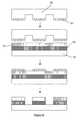
- FIG. 4illustrates a thin silicon substrate 40 supported on a thick glass carrier 41 which is supported at its periphery by supporting members 42 .
- a force F applied to an upper surface of a central part of the substrate 40causes significant downward deflection of the substrate 40 and carrier 41 leading to deformation of a volume of imprintable medium (e.g., curable resin—not shown) provided on the upper surface of the substrate 40 .
- imprintable mediume.g., curable resin—not shown
- FIG. 5illustrates an embodiment in which a compensating force F′ is applied underneath the substrate 40 and carrier 41 , on the opposing side to which the stamping force F is applied by a template (not shown).
- the value of F′is chosen to be approximately equal and opposite to F.
- the provision of the compensating force F′substantially eliminates bending of the substrate 40 and carrier 41 .
- the total compression of the substrate and carriermay be of the order of 400 nm. It may be desirable for the value of F′ to be slightly larger than F so as to raise the area A of the substrate 40 to compensate for compression of this area of the substrate 40 .
- the compensating force F′is applied in an embodiment via a spring or other compensating member positioned beneath the substrate.
- the spring or other compensating memberis moveable underneath the substrate in accordance with movement of the template above the substrate so as to maintain the effectiveness of the “cushioning” provided by the spring.
- a plurality of springs or other compensating membersmay be provided beneath the substrate.
- the other compensating membermay be a piezoelectrically actuated member and/or a rod displaceably mounted within a coil capable of carrying an electric current (e.g. a Lorentz motor).
- the substratewill incur damage if subjected to a force above a particular threshold.
- the force imparted by the template to the substratecan be held below this threshold by placing the template in a caddy which releases the template if the force is above the threshold.
- a template 70is attached to a board 71 .
- the board 71is biased against support blocks 72 , and has notches 73 formed between the points of support and the region of attachment to the template 70 .
- the notches 73are weak points in the board, and if the reactive force F 3 between the template and the substrate exceeds the force required to break the board at the notches, the board 71 will break and the template will be allowed to move upwards before it causes unwanted damage. This system will typically use a replacement board each time the threshold force is exceeded.
- the templateis attached at an upper end to a spring which acts to hold the template in place when it exceeds the threshold force. This prevents the patterned face of the template from being damaged by contact with other elements.
- FIG. 8illustrates a further method for separating a template 80 from an imprinted medium 81 supported on a transfer layer 82 which may reduce a problem connected with pulling or peeling the template 80 from the imprinted medium 81 .
- Pressurized fluide.g. air or liquid
- the imprinted medium 81is subjected to a compressive force rather than an extensive force, which imposes less stringent requirements on the strength of the imprinted medium 81 .
- By temporarily compressing the imprinted medium 81the chance of it sticking to the template 80 is reduced.
- the imprinted medium 81will typically shrink slightly following curing or polymerization, small gaps 83 are often present between regions of the imprinted medium 81 and the template 80 following imprinting, which can be exploited by the introduction of the pressurized fluid to urge the template 80 and the imprinted medium 81 apart.
Landscapes
- Engineering & Computer Science (AREA)
- Chemical & Material Sciences (AREA)
- Nanotechnology (AREA)
- Physics & Mathematics (AREA)
- Crystallography & Structural Chemistry (AREA)
- General Physics & Mathematics (AREA)
- Theoretical Computer Science (AREA)
- Organic Chemistry (AREA)
- General Chemical & Material Sciences (AREA)
- Mathematical Physics (AREA)
- Materials Engineering (AREA)
- Metallurgy (AREA)
- Chemical Kinetics & Catalysis (AREA)
- Condensed Matter Physics & Semiconductors (AREA)
- Mechanical Engineering (AREA)
- Manufacturing & Machinery (AREA)
- Exposure Of Semiconductors, Excluding Electron Or Ion Beam Exposure (AREA)
- Micromachines (AREA)
- Shaping Of Tube Ends By Bending Or Straightening (AREA)
Abstract
Description
Claims (15)
Priority Applications (3)
| Application Number | Priority Date | Filing Date | Title |
|---|---|---|---|
| US11/155,941US7922474B2 (en) | 2005-02-17 | 2005-02-17 | Imprint lithography |
| JP2006039322AJP4459914B2 (en) | 2005-02-17 | 2006-02-16 | Imprint lithography |
| JP2010003894AJP5249250B2 (en) | 2005-02-17 | 2010-01-12 | Imprint method and imprint apparatus |
Applications Claiming Priority (1)
| Application Number | Priority Date | Filing Date | Title |
|---|---|---|---|
| US11/155,941US7922474B2 (en) | 2005-02-17 | 2005-02-17 | Imprint lithography |
Publications (2)
| Publication Number | Publication Date |
|---|---|
| US20060180952A1 US20060180952A1 (en) | 2006-08-17 |
| US7922474B2true US7922474B2 (en) | 2011-04-12 |
Family
ID=36814864
Family Applications (1)
| Application Number | Title | Priority Date | Filing Date |
|---|---|---|---|
| US11/155,941Expired - Fee RelatedUS7922474B2 (en) | 2005-02-17 | 2005-02-17 | Imprint lithography |
Country Status (2)
| Country | Link |
|---|---|
| US (1) | US7922474B2 (en) |
| JP (2) | JP4459914B2 (en) |
Families Citing this family (9)
| Publication number | Priority date | Publication date | Assignee | Title |
|---|---|---|---|---|
| US20080160129A1 (en) | 2006-05-11 | 2008-07-03 | Molecular Imprints, Inc. | Template Having a Varying Thickness to Facilitate Expelling a Gas Positioned Between a Substrate and the Template |
| US7922474B2 (en)* | 2005-02-17 | 2011-04-12 | Asml Netherlands B.V. | Imprint lithography |
| US7789294B2 (en)* | 2005-02-18 | 2010-09-07 | Ebet Systems Pty Ltd | System and method for monitoring a validator |
| JP4595120B2 (en)* | 2005-05-27 | 2010-12-08 | 独立行政法人産業技術総合研究所 | Imprint method and apparatus by back surface pressurization |
| US7613538B2 (en)* | 2006-07-24 | 2009-11-03 | Hewlett-Packard Development Company, L.P. | Compensation for distortion in contact lithography |
| JP2010503993A (en)* | 2006-09-19 | 2010-02-04 | モレキュラー・インプリンツ・インコーポレーテッド | Improved etching techniques for lift-off patterning |
| US8652393B2 (en)* | 2008-10-24 | 2014-02-18 | Molecular Imprints, Inc. | Strain and kinetics control during separation phase of imprint process |
| WO2012016744A1 (en) | 2010-08-05 | 2012-02-09 | Asml Netherlands B.V. | Imprint lithography |
| JP5995567B2 (en)* | 2012-07-12 | 2016-09-21 | キヤノン株式会社 | Imprint apparatus and article manufacturing method using the same |
Citations (51)
| Publication number | Priority date | Publication date | Assignee | Title |
|---|---|---|---|---|
| US5512131A (en) | 1993-10-04 | 1996-04-30 | President And Fellows Of Harvard College | Formation of microstamped patterns on surfaces and derivative articles |
| US5772905A (en) | 1995-11-15 | 1998-06-30 | Regents Of The University Of Minnesota | Nanoimprint lithography |
| US6165911A (en) | 1999-12-29 | 2000-12-26 | Calveley; Peter Braden | Method of patterning a metal layer |
| WO2001079592A1 (en) | 2000-04-13 | 2001-10-25 | Obducat Aktiebolag | Apparatus and method for electrochemical processing of substrates |
| WO2001079591A1 (en) | 2000-04-13 | 2001-10-25 | Obducat Aktiebolag | Apparatus and method for electrochemical processing of substrates |
| US6309580B1 (en) | 1995-11-15 | 2001-10-30 | Regents Of The University Of Minnesota | Release surfaces, particularly for use in nanoimprint lithography |
| US6334960B1 (en) | 1999-03-11 | 2002-01-01 | Board Of Regents, The University Of Texas System | Step and flash imprint lithography |
| US6365059B1 (en) | 2000-04-28 | 2002-04-02 | Alexander Pechenik | Method for making a nano-stamp and for forming, with the stamp, nano-size elements on a substrate |
| US6375870B1 (en) | 1998-11-17 | 2002-04-23 | Corning Incorporated | Replicating a nanoscale pattern |
| US20020094496A1 (en) | 2000-07-17 | 2002-07-18 | Choi Byung J. | Method and system of automatic fluid dispensing for imprint lithography processes |
| US20020093122A1 (en) | 2000-08-01 | 2002-07-18 | Choi Byung J. | Methods for high-precision gap and orientation sensing between a transparent template and substrate for imprint lithography |
| US20020132482A1 (en) | 2000-07-18 | 2002-09-19 | Chou Stephen Y. | Fluid pressure imprint lithography |
| US6518189B1 (en) | 1995-11-15 | 2003-02-11 | Regents Of The University Of Minnesota | Method and apparatus for high density nanostructures |
| JP2003077867A (en) | 2001-09-04 | 2003-03-14 | National Institute Of Advanced Industrial & Technology | Moving stage for imprint lithography |
| US20030080472A1 (en) | 2001-10-29 | 2003-05-01 | Chou Stephen Y. | Lithographic method with bonded release layer for molding small patterns |
| US20030081193A1 (en) | 2001-06-01 | 2003-05-01 | White Donald L. | Holder, system, and process for improving overlay in lithography |
| US20030127580A1 (en) | 2000-01-21 | 2003-07-10 | Tornjorn Ling | Mold for nano imprinting |
| US20030139042A1 (en) | 2000-05-24 | 2003-07-24 | Babak Heidari | Method in connection with the production of a template and the template thus produced |
| US20030141291A1 (en) | 2000-02-23 | 2003-07-31 | Babak Heidari | Device for homogeneous heating of an object |
| US20030159608A1 (en) | 1999-12-10 | 2003-08-28 | Babak Heidari | Device and method in connection with the production of structures |
| US20030170053A1 (en) | 2000-03-15 | 2003-09-11 | Lars Montelius | Device for transferring a pattern to an object |
| US20030189273A1 (en) | 2002-04-04 | 2003-10-09 | Lennart Olsson | Imprint method and device |
| US20030215577A1 (en)* | 2002-05-16 | 2003-11-20 | Willson Carlton Grant | Method and system for fabricating nanoscale patterns in light curable compositions using an electric field |
| US6656341B2 (en) | 2000-09-18 | 2003-12-02 | Obducat Aktiebolag | Method of etching, as well as frame element, mask and prefabricated substrate element for use in such etching |
| WO2003099536A1 (en) | 2002-05-24 | 2003-12-04 | Chou Stephen Y | Methods and apparatus of field-induced pressure imprint lithography |
| US20040005444A1 (en) | 2000-04-18 | 2004-01-08 | Babak Heidari | Substrate for and a process in connection with the product of structures |
| US20040009673A1 (en) | 2002-07-11 | 2004-01-15 | Sreenivasan Sidlgata V. | Method and system for imprint lithography using an electric field |
| US20040022888A1 (en) | 2002-08-01 | 2004-02-05 | Sreenivasan Sidlgata V. | Alignment systems for imprint lithography |
| US20040021866A1 (en) | 2002-08-01 | 2004-02-05 | Watts Michael P.C. | Scatterometry alignment for imprint lithography |
| US6696220B2 (en) | 2000-10-12 | 2004-02-24 | Board Of Regents, The University Of Texas System | Template for room temperature, low pressure micro-and nano-imprint lithography |
| US20040036201A1 (en) | 2000-07-18 | 2004-02-26 | Princeton University | Methods and apparatus of field-induced pressure imprint lithography |
| US20040046288A1 (en) | 2000-07-18 | 2004-03-11 | Chou Stephen Y. | Laset assisted direct imprint lithography |
| US20040080734A1 (en)* | 2002-10-17 | 2004-04-29 | Yukio Taniguchi | Method and apparatus for forming pattern on thin substrate or the like |
| US20040081798A1 (en) | 2002-10-24 | 2004-04-29 | Heon Lee | Hardened nano-imprinting stamp |
| US20040124566A1 (en) | 2002-07-11 | 2004-07-01 | Sreenivasan Sidlgata V. | Step and repeat imprint lithography processes |
| US20040149367A1 (en) | 2002-06-20 | 2004-08-05 | Lennart Olsson | Devices and methods for aligning a stamp and a substrate |
| US20040169003A1 (en) | 2002-10-24 | 2004-09-02 | Heon Lee | Micro-casted silicon carbide nano-imprinting stamp |
| US20040192041A1 (en)* | 2003-03-27 | 2004-09-30 | Jun-Ho Jeong | UV nanoimprint lithography process using elementwise embossed stamp and selectively additive pressurization |
| US20040209470A1 (en) | 2003-04-17 | 2004-10-21 | Bajorek Christopher H. | Isothermal imprinting |
| US20040219249A1 (en) | 2003-05-02 | 2004-11-04 | Yong-Chen Chung | Uniform pressing apparatus |
| US20040219461A1 (en) | 2003-05-02 | 2004-11-04 | Yong-Chen Chung | Parallelism adjustment device |
| US6829988B2 (en)* | 2003-05-16 | 2004-12-14 | Suss Microtec, Inc. | Nanoimprinting apparatus and method |
| US20050039618A1 (en) | 2001-07-05 | 2005-02-24 | Babak Heidari | Stamp having an antisticking layer and a method of forming of repairing such a stamp |
| US20050064054A1 (en) | 2003-09-24 | 2005-03-24 | Canon Kabushiki Kaisha | Pattern forming apparatus |
| US6921615B2 (en) | 2000-07-16 | 2005-07-26 | Board Of Regents, The University Of Texas System | High-resolution overlay alignment methods for imprint lithography |
| US20050263077A1 (en) | 2004-05-28 | 2005-12-01 | Board Of Regents, The University Of Texas System | Adaptive shape substrate support method |
| JP2006100723A (en) | 2004-09-30 | 2006-04-13 | Toshiba Corp | Imprint apparatus and method |
| US20060273488A1 (en)* | 2005-06-07 | 2006-12-07 | Canon Kabushiki Kaisha | Processing apparatus, processing method, and process for producing chip |
| US7168939B2 (en)* | 2004-02-26 | 2007-01-30 | Hitachi Global Storage Technologies Netherlands Bv | System, method, and apparatus for multilevel UV molding lithography for air bearing surface patterning |
| US7207871B1 (en)* | 2005-10-06 | 2007-04-24 | Applied Materials, Inc. | Carrier head with multiple chambers |
| US7618752B2 (en)* | 2006-10-12 | 2009-11-17 | Hewlett-Packard Development Company, L.P. | Deformation-based contact lithography systems, apparatus and methods |
Family Cites Families (7)
| Publication number | Priority date | Publication date | Assignee | Title |
|---|---|---|---|---|
| JP3187014B2 (en)* | 1990-01-24 | 2001-07-11 | ホーヤ株式会社 | Lens mold |
| JP2691148B2 (en)* | 1995-08-22 | 1997-12-17 | エドカ工業株式会社 | Manufacturing method of sheet lens |
| JP2004034300A (en)* | 2002-06-28 | 2004-02-05 | Elionix Kk | Micro-extruder |
| JP4317375B2 (en)* | 2003-03-20 | 2009-08-19 | 株式会社日立製作所 | Nanoprint apparatus and fine structure transfer method |
| JP2005085965A (en)* | 2003-09-08 | 2005-03-31 | Canon Inc | Near-field exposure mask, near-field exposure method, and near-field exposure apparatus |
| JP4455092B2 (en)* | 2004-02-20 | 2010-04-21 | キヤノン株式会社 | Processing apparatus and processing method |
| US7922474B2 (en)* | 2005-02-17 | 2011-04-12 | Asml Netherlands B.V. | Imprint lithography |
- 2005
- 2005-02-17USUS11/155,941patent/US7922474B2/ennot_activeExpired - Fee Related
- 2006
- 2006-02-16JPJP2006039322Apatent/JP4459914B2/ennot_activeExpired - Fee Related
- 2010
- 2010-01-12JPJP2010003894Apatent/JP5249250B2/ennot_activeExpired - Fee Related
Patent Citations (60)
| Publication number | Priority date | Publication date | Assignee | Title |
|---|---|---|---|---|
| US5512131A (en) | 1993-10-04 | 1996-04-30 | President And Fellows Of Harvard College | Formation of microstamped patterns on surfaces and derivative articles |
| US5772905A (en) | 1995-11-15 | 1998-06-30 | Regents Of The University Of Minnesota | Nanoimprint lithography |
| US6518189B1 (en) | 1995-11-15 | 2003-02-11 | Regents Of The University Of Minnesota | Method and apparatus for high density nanostructures |
| US6309580B1 (en) | 1995-11-15 | 2001-10-30 | Regents Of The University Of Minnesota | Release surfaces, particularly for use in nanoimprint lithography |
| US20020167117A1 (en) | 1998-06-30 | 2002-11-14 | Regents Of The University Of Minnesota | Release surfaces, particularly for use in nanoimprint lithography |
| US20030034329A1 (en) | 1998-06-30 | 2003-02-20 | Chou Stephen Y. | Lithographic method for molding pattern with nanoscale depth |
| US6375870B1 (en) | 1998-11-17 | 2002-04-23 | Corning Incorporated | Replicating a nanoscale pattern |
| US6719915B2 (en) | 1999-03-11 | 2004-04-13 | Board Of Regents, The University Of Texas System | Step and flash imprint lithography |
| US6334960B1 (en) | 1999-03-11 | 2002-01-01 | Board Of Regents, The University Of Texas System | Step and flash imprint lithography |
| US20030159608A1 (en) | 1999-12-10 | 2003-08-28 | Babak Heidari | Device and method in connection with the production of structures |
| US6165911A (en) | 1999-12-29 | 2000-12-26 | Calveley; Peter Braden | Method of patterning a metal layer |
| US20030127580A1 (en) | 2000-01-21 | 2003-07-10 | Tornjorn Ling | Mold for nano imprinting |
| US20030141291A1 (en) | 2000-02-23 | 2003-07-31 | Babak Heidari | Device for homogeneous heating of an object |
| US20030170053A1 (en) | 2000-03-15 | 2003-09-11 | Lars Montelius | Device for transferring a pattern to an object |
| WO2001079592A1 (en) | 2000-04-13 | 2001-10-25 | Obducat Aktiebolag | Apparatus and method for electrochemical processing of substrates |
| WO2001079591A1 (en) | 2000-04-13 | 2001-10-25 | Obducat Aktiebolag | Apparatus and method for electrochemical processing of substrates |
| US20040005444A1 (en) | 2000-04-18 | 2004-01-08 | Babak Heidari | Substrate for and a process in connection with the product of structures |
| US6365059B1 (en) | 2000-04-28 | 2002-04-02 | Alexander Pechenik | Method for making a nano-stamp and for forming, with the stamp, nano-size elements on a substrate |
| US20030139042A1 (en) | 2000-05-24 | 2003-07-24 | Babak Heidari | Method in connection with the production of a template and the template thus produced |
| US6921615B2 (en) | 2000-07-16 | 2005-07-26 | Board Of Regents, The University Of Texas System | High-resolution overlay alignment methods for imprint lithography |
| US20020094496A1 (en) | 2000-07-17 | 2002-07-18 | Choi Byung J. | Method and system of automatic fluid dispensing for imprint lithography processes |
| US6482742B1 (en) | 2000-07-18 | 2002-11-19 | Stephen Y. Chou | Fluid pressure imprint lithography |
| US20040046288A1 (en) | 2000-07-18 | 2004-03-11 | Chou Stephen Y. | Laset assisted direct imprint lithography |
| US20020177319A1 (en) | 2000-07-18 | 2002-11-28 | Chou Stephen Y. | Fluid pressure bonding |
| US20040036201A1 (en) | 2000-07-18 | 2004-02-26 | Princeton University | Methods and apparatus of field-induced pressure imprint lithography |
| US20020132482A1 (en) | 2000-07-18 | 2002-09-19 | Chou Stephen Y. | Fluid pressure imprint lithography |
| US20020093122A1 (en) | 2000-08-01 | 2002-07-18 | Choi Byung J. | Methods for high-precision gap and orientation sensing between a transparent template and substrate for imprint lithography |
| US6656341B2 (en) | 2000-09-18 | 2003-12-02 | Obducat Aktiebolag | Method of etching, as well as frame element, mask and prefabricated substrate element for use in such etching |
| US6696220B2 (en) | 2000-10-12 | 2004-02-24 | Board Of Regents, The University Of Texas System | Template for room temperature, low pressure micro-and nano-imprint lithography |
| US20030081193A1 (en) | 2001-06-01 | 2003-05-01 | White Donald L. | Holder, system, and process for improving overlay in lithography |
| US20050039618A1 (en) | 2001-07-05 | 2005-02-24 | Babak Heidari | Stamp having an antisticking layer and a method of forming of repairing such a stamp |
| JP2003077867A (en) | 2001-09-04 | 2003-03-14 | National Institute Of Advanced Industrial & Technology | Moving stage for imprint lithography |
| US20030080472A1 (en) | 2001-10-29 | 2003-05-01 | Chou Stephen Y. | Lithographic method with bonded release layer for molding small patterns |
| US20030080471A1 (en) | 2001-10-29 | 2003-05-01 | Chou Stephen Y. | Lithographic method for molding pattern with nanoscale features |
| US20030189273A1 (en) | 2002-04-04 | 2003-10-09 | Lennart Olsson | Imprint method and device |
| US20040200411A1 (en) | 2002-05-16 | 2004-10-14 | The Board Of Regents, The University Of Texas System | Apparatus for fabricating nanoscale patterns in light curable compositions using an electric field |
| US20030215577A1 (en)* | 2002-05-16 | 2003-11-20 | Willson Carlton Grant | Method and system for fabricating nanoscale patterns in light curable compositions using an electric field |
| WO2003099536A1 (en) | 2002-05-24 | 2003-12-04 | Chou Stephen Y | Methods and apparatus of field-induced pressure imprint lithography |
| US20040149367A1 (en) | 2002-06-20 | 2004-08-05 | Lennart Olsson | Devices and methods for aligning a stamp and a substrate |
| US20040124566A1 (en) | 2002-07-11 | 2004-07-01 | Sreenivasan Sidlgata V. | Step and repeat imprint lithography processes |
| US20040009673A1 (en) | 2002-07-11 | 2004-01-15 | Sreenivasan Sidlgata V. | Method and system for imprint lithography using an electric field |
| US20040022888A1 (en) | 2002-08-01 | 2004-02-05 | Sreenivasan Sidlgata V. | Alignment systems for imprint lithography |
| US20040021866A1 (en) | 2002-08-01 | 2004-02-05 | Watts Michael P.C. | Scatterometry alignment for imprint lithography |
| US20040080734A1 (en)* | 2002-10-17 | 2004-04-29 | Yukio Taniguchi | Method and apparatus for forming pattern on thin substrate or the like |
| US20040081798A1 (en) | 2002-10-24 | 2004-04-29 | Heon Lee | Hardened nano-imprinting stamp |
| US20040169003A1 (en) | 2002-10-24 | 2004-09-02 | Heon Lee | Micro-casted silicon carbide nano-imprinting stamp |
| US6943117B2 (en)* | 2003-03-27 | 2005-09-13 | Korea Institute Of Machinery & Materials | UV nanoimprint lithography process using elementwise embossed stamp and selectively additive pressurization |
| WO2004086471A1 (en) | 2003-03-27 | 2004-10-07 | Korea Institute Of Machinery & Materials | Uv nanoimprint lithography process using elementwise embossed stamp and selectively additive pressurization |
| US20040192041A1 (en)* | 2003-03-27 | 2004-09-30 | Jun-Ho Jeong | UV nanoimprint lithography process using elementwise embossed stamp and selectively additive pressurization |
| US20040209470A1 (en) | 2003-04-17 | 2004-10-21 | Bajorek Christopher H. | Isothermal imprinting |
| US20040219249A1 (en) | 2003-05-02 | 2004-11-04 | Yong-Chen Chung | Uniform pressing apparatus |
| US20040219461A1 (en) | 2003-05-02 | 2004-11-04 | Yong-Chen Chung | Parallelism adjustment device |
| US6829988B2 (en)* | 2003-05-16 | 2004-12-14 | Suss Microtec, Inc. | Nanoimprinting apparatus and method |
| US20050064054A1 (en) | 2003-09-24 | 2005-03-24 | Canon Kabushiki Kaisha | Pattern forming apparatus |
| US7168939B2 (en)* | 2004-02-26 | 2007-01-30 | Hitachi Global Storage Technologies Netherlands Bv | System, method, and apparatus for multilevel UV molding lithography for air bearing surface patterning |
| US20050263077A1 (en) | 2004-05-28 | 2005-12-01 | Board Of Regents, The University Of Texas System | Adaptive shape substrate support method |
| JP2006100723A (en) | 2004-09-30 | 2006-04-13 | Toshiba Corp | Imprint apparatus and method |
| US20060273488A1 (en)* | 2005-06-07 | 2006-12-07 | Canon Kabushiki Kaisha | Processing apparatus, processing method, and process for producing chip |
| US7207871B1 (en)* | 2005-10-06 | 2007-04-24 | Applied Materials, Inc. | Carrier head with multiple chambers |
| US7618752B2 (en)* | 2006-10-12 | 2009-11-17 | Hewlett-Packard Development Company, L.P. | Deformation-based contact lithography systems, apparatus and methods |
Non-Patent Citations (3)
| Title |
|---|
| English translation of Official Action issued on Mar. 11, 2009 in Japanese Application No. 2006-039322. |
| Heon Lee et al. "Full wafer scale near zero residual nano-imprinting lithography using UV curable monomer solution", Microelectronic Engineering 77, pp. 42-47, (2005). |
| Stephen Y. Chou, et al., "Nanoimprint Lithography", J. Vac. Sci. Technol. B 14(6), Nov./Dec. 1996, pp. 4129-4133. |
Also Published As
| Publication number | Publication date |
|---|---|
| JP5249250B2 (en) | 2013-07-31 |
| US20060180952A1 (en) | 2006-08-17 |
| JP2006229232A (en) | 2006-08-31 |
| JP2010087533A (en) | 2010-04-15 |
| JP4459914B2 (en) | 2010-04-28 |
Similar Documents
| Publication | Publication Date | Title |
|---|---|---|
| US10025206B2 (en) | Imprint lithography | |
| US7363854B2 (en) | System and method for patterning both sides of a substrate utilizing imprint lithography | |
| US8571318B2 (en) | Imprint lithography | |
| US9341944B2 (en) | Imprint lithography | |
| US7862756B2 (en) | Imprint lithography | |
| US8318253B2 (en) | Imprint lithography | |
| US7418902B2 (en) | Imprint lithography including alignment | |
| KR100855725B1 (en) | Imprint lithography | |
| US8100684B2 (en) | Imprint lithography | |
| US7943080B2 (en) | Alignment for imprint lithography | |
| JP5249250B2 (en) | Imprint method and imprint apparatus | |
| US7490547B2 (en) | Imprint lithography | |
| US7611348B2 (en) | Imprint lithography | |
| US20070023976A1 (en) | Imprint lithography | |
| US20060144814A1 (en) | Imprint lithography |
Legal Events
| Date | Code | Title | Description |
|---|---|---|---|
| AS | Assignment | Owner name:ASML NETHERLANDS B.V., NETHERLANDS Free format text:ASSIGNMENT OF ASSIGNORS INTEREST;ASSIGNORS:KRUIJT-STEGEMAN, YVONNE WENDELA;JANSSEN, HENRICUS WILHELMUS ALOYSIUS;KOLESNYCHENKO, ALEKSEY YURIEVICH;AND OTHERS;SIGNING DATES FROM 20050818 TO 20050922;REEL/FRAME:017070/0070 Owner name:ASML NETHERLANDS B.V., NETHERLANDS Free format text:ASSIGNMENT OF ASSIGNORS INTEREST;ASSIGNORS:KRUIJT-STEGEMAN, YVONNE WENDELA;JANSSEN, HENRICUS WILHELMUS ALOYSIUS;KOLESNYCHENKO, ALEKSEY YURIEVICH;AND OTHERS;REEL/FRAME:017070/0070;SIGNING DATES FROM 20050818 TO 20050922 | |
| FEPP | Fee payment procedure | Free format text:PAYOR NUMBER ASSIGNED (ORIGINAL EVENT CODE: ASPN); ENTITY STATUS OF PATENT OWNER: LARGE ENTITY | |
| STCF | Information on status: patent grant | Free format text:PATENTED CASE | |
| FPAY | Fee payment | Year of fee payment:4 | |
| MAFP | Maintenance fee payment | Free format text:PAYMENT OF MAINTENANCE FEE, 8TH YEAR, LARGE ENTITY (ORIGINAL EVENT CODE: M1552); ENTITY STATUS OF PATENT OWNER: LARGE ENTITY Year of fee payment:8 | |
| FEPP | Fee payment procedure | Free format text:MAINTENANCE FEE REMINDER MAILED (ORIGINAL EVENT CODE: REM.); ENTITY STATUS OF PATENT OWNER: LARGE ENTITY | |
| LAPS | Lapse for failure to pay maintenance fees | Free format text:PATENT EXPIRED FOR FAILURE TO PAY MAINTENANCE FEES (ORIGINAL EVENT CODE: EXP.); ENTITY STATUS OF PATENT OWNER: LARGE ENTITY | |
| STCH | Information on status: patent discontinuation | Free format text:PATENT EXPIRED DUE TO NONPAYMENT OF MAINTENANCE FEES UNDER 37 CFR 1.362 | |
| FP | Lapsed due to failure to pay maintenance fee | Effective date:20230412 |