US7920596B2 - Method for high speed framing and a device having framing capabilities - Google Patents
Method for high speed framing and a device having framing capabilitiesDownload PDFInfo
- Publication number
- US7920596B2 US7920596B2US12/160,007US16000706AUS7920596B2US 7920596 B2US7920596 B2US 7920596B2US 16000706 AUS16000706 AUS 16000706AUS 7920596 B2US7920596 B2US 7920596B2
- Authority
- US
- United States
- Prior art keywords
- data
- framed
- framer
- data chunk
- operation sequence
- Prior art date
- Legal status (The legal status is an assumption and is not a legal conclusion. Google has not performed a legal analysis and makes no representation as to the accuracy of the status listed.)
- Active, expires
Links
Images


Classifications
- H—ELECTRICITY
- H04—ELECTRIC COMMUNICATION TECHNIQUE
- H04L—TRANSMISSION OF DIGITAL INFORMATION, e.g. TELEGRAPHIC COMMUNICATION
- H04L69/00—Network arrangements, protocols or services independent of the application payload and not provided for in the other groups of this subclass
- H04L69/30—Definitions, standards or architectural aspects of layered protocol stacks
- H04L69/32—Architecture of open systems interconnection [OSI] 7-layer type protocol stacks, e.g. the interfaces between the data link level and the physical level
- H04L69/322—Intralayer communication protocols among peer entities or protocol data unit [PDU] definitions
- H04L69/324—Intralayer communication protocols among peer entities or protocol data unit [PDU] definitions in the data link layer [OSI layer 2], e.g. HDLC
Definitions
- the inventionrelates to methods for high-speed framing and a device having framing capabilities, especially in telecommunication integrated circuits.
- Modern telecommunication devicesare required to manage large amounts of communication channels. This management process includes processing information frames (or packets) according to one or more telecommunication protocols. Some of these stages are referred to as framing.
- Various framersare known in the art.
- U.S. Pat. No. 6,442,178 of Arato et al., titled “System and method for data alignment in a communication system”describes a prior art framer.
- HDLCis a commonly used framing protocol.
- HDLC signalsmark an end or beginning of a frame by an open or close frame flag that includes a sequence of six consecutive “1” bits.
- HDLC framersinsert a zero bit after every sequence of five “1” bits of data in order to guarantee the identification of the end frame flag.
- framersare also capable of performing additional operations such as performing CRC error correction algorithms.
- the framing devices of this typecan support multiple protocols that are based, but not necessarily so, on HDLC, such as Signaling system No 7, PPP, etc.
- the metadata of a multi channel transmittercan include global (relevant to all channels) parameters, channel specific parameters, channel buffer descriptors and the like. Data can be stored in buffers that are pointed by pointers within buffer descriptors.
- Modern communication devicesare required to operate at ever growing rates.
- Various processing componentssuch as framers are required to operate more quickly.
- One way of increasing the throughput of framersis to duplicate them, but this is a costly solution.
- FIG. 1illustrates a device according to an embodiment of the invention
- FIG. 2illustrates a device according to another embodiment of the invention
- FIG. 3illustrates a device according to a further embodiment of the invention
- FIG. 4is a flow chart of a method for framing data according to an embodiment of the invention.
- FIG. 5illustrates an operation sequence according to an embodiment of the invention.
- a device having framing capabilitiesincludes a framer that is adapted to frame a data chunk per data chunk frame operation.
- the size of the data chunkis conveniently fixed.
- a typical data chunk frame operationis preceded by fetching data (one or more data chunks) as well as fetching metadata required for framing the data.
- the metadatacan include masks, instructions, status and control information and the like.
- the metadatacan include buffer descriptors.
- the aggregate size of metadataexceeds the size of the data chunk.
- the data and metadataare fetched from a memory unit that can be an internal or an external memory unit.
- a data chunk frame operationcan include framing a data chunk to provide a framed data chunk. This operation can include applying error correction algorithms such as but not limited to the CRC algorithm.
- error correction algorithmssuch as but not limited to the CRC algorithm.
- the inventorsapplied HDLC compliant framing operations but other framing mechanisms known in the art can be applied.
- the devicecan speed the framing process by fetching multiple data chunks as well as fetching metadata required for framing the multiple data chunks. These fetching operations are followed by executing multiple data chunk frame operations.
- Data chunkscan be associated to other chunks. This association is reflected by an option to re-use in one data chunk frame operations the products of a previous data chunk-operation. For example, if two data chunks that belong to a certain communication channel are consecutively framed than at least a portion of the meta-data used during the framing of the first data chunk can be used for framing the second data chunk.
- consecutively framing data chunks that are not associated with each otherwill involve a repetition of a full scale meta-data retrieval sequence.
- consecutively framing data chunks that are associated to each othercan dramatically speed the framing process.
- a framercan use internally stored masks or status information relating to previous framing operations.
- the inventorsused a framer that was capable of framing one byte at a time. In order to frame this data byte thirty fetch and frame related instructions were executed. More than half of these instructions include fetch and/or write instructions. By consecutively framing associated data chunks fewer instructions were executed. The framing of the first byte involved executing thirty instructions while the framing of consecutive associated bytes required only ten instructions.
- a single framermay be asked to frame data that is associated with multiple communication channels.
- the devicecan repetitively perform a data and meta-date fetch operation and then a data chunk frame operation.
- the devicecan fetch (during one or more fetch operations) multiple data chunks and metadata required for framing the data chunks and then perform consecutive data chunk frame operations.
- the framerAfter executing two or more data chunk frame operations the framer can output one or more framed data chunks simultaneously.
- the deviceincludes at least one memory unit that is adapted to store data and metadata required for framing the stored data and a framed data unit.
- the framed data unitcan selectively receive framed data chunks from the framer.
- the framed data unitcan include an internal memory, a multiplexer, a transmitter and the like.
- the frame data unitcan be connected to other data frame transmitters such as physical layer or other lower layer data transmitters.
- the data chunkincludes one or more bytes.
- the framed data chunkscan be slightly larger, due to zero insertion operations or other protocol derived processing.
- the framed data unitcan selectively ignore one or more framed data chunks that are provided during one or more data chunk frame operations.
- the framed data unitusually receives the framed data chunks later on. For example, it is assumed that the framer performs two consecutive data chunk frame operations. After the first data chunk frame operation the framer outputs a first framed data chunk. After the second data chunk frame operation the framer outputs concurrently the first framed data chunk and a second framed data chunk.
- the receiving Framed data unitis adapted to ignore the data chunks and provide the proper acknowledge.
- the framed data unitcan ignore the first framed data chunk that is provided after the first data chunk frame operation. This simplifies the management of framed data chunks and reduces the number of transactions between the framer and the framed data unit.
- a method for framing dataincludes: (i) Storing data and metadata required for framing the stored data at one or more memory devices.
- the datacan include multiple data chunks.
- Executing( 560 ) an operation sequence out of a first operation sequence and a second operation sequence; wherein the first operation sequence comprises a data chunk and metadata fetch operation followed by a data chunk frame operation and wherein the second operation sequence comprises a multiple data chunk fetch operation followed by multiple data chunk frame operations.
- a framerretrieves many instructions before starting to perform a framing operation. These multiple instructions form a framing code that can include multiple conditional branches. For example, a zero can be inserted after a sequence of five “1”. The presence of such sequence is not known in advance, and a conditional branch to a routine that inserts a zero is required. Due to the complexity of the framing code merely applying the code multiple times can greatly simplify the code that is required for executing multiple data chunk frame operations.
- FIG. 1illustrates a device 10 according to an embodiment of the invention.
- Device 10includes a processor 50 , a fetch data unit 45 , a memory unit 20 , a framer 30 and a framed data unit 40 .
- the processor 50is connected to the fetch data unit 45 , to the framer 30 and to the memory unit 20 via a shared bus.
- the processor 50is also connected to framed data unit 40 .
- the framed data unit 40can include one or more interfaces, one or more memory units, one or more multiplexers, transmitters (such as but not limited to MAC layer transmitters, physical layer transmitters) and the like.
- the framed data unit 40can also include various layer receivers. In such a case the framed data unit 40 can send framed data chunks to the framer and request the framer to de-frame the framed data chunks to provide data chunks (also referred to as raw data chunks). It is noted that the requests can be generated by another component.
- the framed data unit 40is adapted to receive framed data chunks from the framer 30 . It can selectively ignore one or more data chunks, conveniently in response to control signals provided by framer 30 .
- Memory unit 20can be connected to higher-level memory units via various buses, DMA controllers and the like. Data and metadata can be fetched from an external memory unit and just then fetched from memory unit 20 , and vice verse. It is noted that the data can be stored in various buffers and that the metadata can include buffer descriptors, HDLS mask and status information and the like.
- the framer 30can fetch multiple data chunks as well as metadata required for framing the data chunks, performs a sequence of data chunk frame operations and provides multiple frame data chunks to the frame data chunk unit 40 .
- the framer 30can operate in a single byte framing mode or in a double byte operational mode.
- the framer 30outputs a control signal (valid output flag) that indicates if the framed data unit 40 should accept the framed data unit that is outputted from the framer 30 or should it be ignored.
- the framer 30For example, assuming that the framer 30 is requested to consecutively frame two associated data chunks.
- the framer 30performs a first data chunk frame operation and generates a first framed data chunk. This first framed data chunk is stored at the framer 30 .
- the frameralso resets a valid output flag and in response the framed data unit 40 ignores the first framed data chunk.
- the framed data unit 40will not initiate a transaction to receive the first framed data chunk and will not store it.
- the framer 30then frames the second data chunk, while using various parameters that were fetched and even optionally updated during the first data chunk framing operation as well as using the framed data chunk. This dramatically speeds the second data chunk frame operation and does not require a change in the code handling a single byte or more then a single byte.
- the frameralso sets the valid output flag and outputs (in parallel or in a serial manner) the first and second framed data chunks to the framed data unit 40 .
- the framed data unit 40receives both framed data chunks and can store them, further process them, multiplex them, and the like.
- the valid output flagis usually set, unless some error occurred.
- the framer 30can also output a single framed data chunk per framing operation and that the framed data unit 40 can receive each framed data chunk.
- the output valid flagis irrelevant in such a scenario.
- the framer 30includes a register file 31 , an input bus interface 38 , a framer controller unit 34 , an error correction unit 33 , a framer circuit 35 , a framer status indictor 32 and an output bus interface 36 .
- the register file 31is connected to the error correction unit 33 , the framer circuit 35 to the input bus interface 36 and to the output but interface 36 .
- the register file 31can store one or more data chunks and metadata required for framing one or more data chunks. It conveniently receives data and metadata via input bus interface 38 and outputs one or more framed data chunks to the output bus interface 36 .
- the framer circuit 35 and the error correction unit 33are adapted to process a data chunk according to metadata associated with the data chunk.
- the framer circuit 35outputs framed data chunks to the output bus interface 36 .
- the framer controller 34controls the operation of various components of framer 30 and can, for example, determine from which entries to fetch data and metadata.
- the framer controller 34may include an address generator unit and a bus transaction unit.
- Each of the interfaces 38 and 36can include one or more buffers.
- the framer controller 34can set or reset various flags (such as valid output flag) that are stored at framer status unit 32 .
- FIG. 2illustrates device 10 ′ according to another embodiment of the invention.
- Device 10 ′ of FIG. 2differs from device 10 of FIG. 1 by: (i) having a framer 30 ′′ that is also adapted to perform de-framing operations, and (ii) having a processor 50 that includes framer 30 .
- Framer 30 ′′differs from framer 30 by including a framer/de-framer circuit 35 ′.
- the error correction unit 33 ′should perform error correction operations and reverse error correction stages. For example in one phase it generates a CRC codeword and in another phase it uses a received CRC codeword to correct errors in the received framed data chunk. Conveniently, the stream of data is reversed during reception operation while the stream of metadata flows at the same direction.
- FIG. 3illustrates a device 10 ′′, according to an embodiment of the invention.
- Device 10includes a general-purpose processor 12 , a security engine 14 , system interface unit 18 , communication engine 200 and multiple ports (not shown). Components 12 , 14 , 18 and 200 are connected to each other by local bus 16 .
- the general-purpose processor 12can include multiple execution units such as but not limited to an integer unit, a branch processing unit, a floating point unit, a load/store unit and a system register unit. It can also include various cache memories, dynamic power management unit, translation look aside buffers, and the like.
- the general-purpose processor 12controls device 10 ′′ and can execute various programs according to the required functionality of device 10 ′′.
- the general-purpose processor 12can be a member of the PowerPCTM family but this is not necessarily so.
- the security engine 14can apply various security mechanisms including encryption based mechanisms and the like.
- System interface unit 18may include some of the following components: external memory controllers, external DDR interface unit, PCI bridge, local bus, bus arbitrator, dual UART unit, dual I 2 C unit, a four channel DMA controller, an interrupt controller, and the like. It is noted that other interfacing components can be used.
- Communication engine 200is a versatile communication component that can manage multiple communication ports that operate according to different communication protocols.
- Communication engine 200includes multiple communication controllers of different types. Each communication controller can manage one or more communication channels. Conveniently, each communication channel is associated with a single virtual buffer. A bi-directional communication channel is viewed as a combination of a receive communication channel and a transmit communication channel. Each such communication channel can have its own information transfer controller, virtual buffers, hardware Buffer, and the like.
- one or more communication channelscan be controlled by a single information transfer controller, but this is not necessarily so.
- the communication engine 200includes two RISC processors 50 and 55 , second level DMA controller 250 , a shared data RAM memory unit 26 , a shared instruction RAM memory unit 28 , scheduler 240 , two first level DMA controllers 252 and 254 , a second memory unit 22 , eight universal communication controllers denoted UCC 1 -UCC 8 110 - 180 , one multi-channel communication controller (MCC 1 ) 190 , two serial peripheral interfaces denoted SP 1 -SP 2 210 - 220 , and two communication interfaces 60 and 65 . It is noted that additional components, such as but not limited to various ports, time slots assigners and the like were omitted for simplicity of explanation.
- the first RISC processor 50is connected to UCC 1 110 , UCC 3 130 , UCC 5 150 , UCC 7 170 , MCC 1 190 , SPI 1 210 , scheduler 240 , shared instruction RAM memory unit 28 and shared data RAM memory unit 260 .
- the access to the first RISC controllercan be managed by scheduler 240 .
- the second RISC processor 55is connected to UCC 2 120 , UCC 4 140 , UCC 6 160 , UCC 8 180 , SPI 2 220 , scheduler 240 , shared instruction RAM memory unit 25 and shared data RAM memory unit 26 .
- the access to the first RISC controllercan be managed by scheduler 240 .
- the first level DMA controllers 252 and 254are connected to the shared data RAM memory unit 26 and to information transfer controllers (not shown) within the various communication controllers.
- Each communication controller out of communication controllers UCC 1 -UCC 8 110 - 180 , MCC 1 190 , and SPI 1 -SPI 2 210 - 220can include transmission paths as well as reception paths.
- a UCCcan support the following communication protocols and interfaces (not all simultaneously): 10/100 Mbps Ethernet, 1000 Mpbs Ethernet, IPv4 and IPv6, L2 Ethernet switching using, ATM protocol via UTOPIA interface, various types of HDLC, UART, and BISYNC.
- MCC 1 190supports two hundred and fifty six HDLC or transparent channels, one hundred and twenty eight SS#7 channels or multiple channels that can be multiplexed to one or more TDM interfaces.
- the communication engine 200can include a controller (not shown) as well as an interrupt unit that coordinate the various components of the communication engine, as well as to enable the communication engine 200 to communicate with general-purpose processor 12 , security engine 14 and system interface unit 16 .
- first level DMA controller 310serves communication controllers UCC 1 , UCC 3 , UCC 5 , UCC 7 , MCC 1 and SPI 1 110 , 130 , 150 , 170 , 190 and 210 respectively
- first level DMA controller 252serves communication controllers UCC 2 , UCC 4 , UCC 6 , UCC 8 and SPI 2 120 , 140 , 160 , 180 and 220 respectively.
- Communication engine 200can include multiple components that are analogues to the components of FIG. 1 or FIG. 2 . It is assumed that each RISC processor (out of 50 and 55 ) includes a framer such as framer 30 of FIG. 1 or framer 30 ′ of FIG. 2 .
- first RISC processor 30includes framer 30 while second RISC processor 55 includes framer 30 ′ that is analogues to framer 30 .
- Memory unit 20 of FIG. 1can includes shared data memory RAM 26 and shared instruction RAM memory unit 28 . Metadata can be stored in both of these memory units.
- the fetch data unit 45 of FIG. 1can be an internal component of each of the RISC processors 50 and 55 or can be a full scale DMA controller.
- the framed data unit 40can include any of the multiple communication controllers UCC 1 -UCC 8 , MCC 190 an as well as first and second communication interfaces 60 and 65 and even include first and second physical layer units 80 and 90 .
- the framed data unit 40sends requests to receive framed data chunks (during a transmission phase) or to receive framed data chunks (during a reception phase).
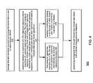
- FIG. 4illustrates a flow chart of method 500 , according to an embodiment of the invention.
- Method 500starts by stage 520 of storing data and metadata required for framing the stored data at one or more memory device.
- data and metadataare provided to shared data RAM memory unit 26 and to shared instruction RAM/ROM memory unit 28 .
- This stagecan involve executing one or more fetch operations from the second memory unit 22 , by the second level DMA controller 250 .
- Stage 520is followed by stage 540 of selecting between an execution of a first operation sequence and an execution of a second operation sequence.
- the first operation sequenceincludes a data chunk and metadata fetch operation followed by a data chunk frame operation.
- the second operation sequenceincludes a multiple data chunk fetch operation followed by multiple data chunk frame operations.
- the selectionis responsive to a predefined value of a certain control signal or a certain field within a memory unit.
- the selectioncan be made in advance to the framing process, by a programmer or by a user that can enter a selection parameter. Conveniently, the amount of consecutive data chunk frame operation can also be provided.
- stage 540can precede stage 520 .
- method 500can alternatively include receiving a selection indication and in response jumping to stage 560 of performing the selected operation.
- Stage 540is followed by stage 560 of executing an operation sequence out of the first operation sequence and a second operation sequence.
- the executionis conveniently responsive to selection made in stage 540 .
- stage 560includes executing at least one data chunk frame operation by a framer that is adapted to frame a single data chunk per one data chunk frame operation.
- a framerthat is adapted to frame a single data chunk per one data chunk frame operation.
- an execution of the second operation sequenceincludes generating multiple framed data chunks during the multiple data chunk frame operations and ignoring at least one of the multiple framed data chunks.
- the second operation sequenceincludes two data chunk frame operations.
- the second operation sequenceincludes two data chunk frame operations; and wherein the executing includes requesting to ignore a single data chunk that is outputted after a certain data chunk frame operation and requesting to receive a pair of data chunks that are outputted after a consecutive data chunk frame operation.
- stage 560includes temporarily storing one or more framed data chunks. These framed data chunks can be stored at the framer. This storage can allow to concurrently output multiple framed data chunks to the framed data unit, thus reducing the number of transactions between the framer and the framed data chunk unit. It is noted that the stored frame data chunks can be erased after they are accepted by the framed data unit.
- method 500further includes stage 570 of sending a notification relating to an amount of valid framed data chunks concurrently outputted by a framer.
- Stages 560 and 570are followed by stage 590 of repetitively generating multiplexes that include framed data chunks associated with different communication channels.
- a single multiplexcan include fewer data chunks (or one data chunks) than the number of data chunks that are outputted by a framer, thus the excessive framed data chunks can be temporarily stored.
- method 500includes concurrently outputting framed data chunks that belong to multiple multiplexes.
- the second operation sequenceis a fraction of the first operation sequence and replaces it in the second operation. In the first operation sequence the framed data unit will ignore any transaction from the framer allowing the use of the same code, conditional branches and conditional jumps as the first operation sequence.
- FIG. 5illustrates an operation sequence 600 according to an embodiment of the invention.
- Operation sequence 600starts by stage 610 of initializing a framer.
- the initializationcan involve fetching one or more data chunks and metadata required to the framing of the one or more data-chunks.
- the data chunkis one byte long and up to two data chunks can be fetched during stage 610 .
- Stage 610is followed by stage 620 of receiving a selection indication that determines whether one data chunk or multiple data chunks should be framed in a sequential manner. If one data chunk is to be framed then stage 620 is followed by stage 630 of framing the data chunk and sending a framed data chunk to a framed data unit.
- stage 620is followed by stage 640 of framing a first data chunk (out of the data chunks that were fetched during stage 610 ) to provide a first framed data chunk, storing the first data chunk and resetting a valid output flag to indicate that an outputted data chunk (or dummy data chunk) should be ignored.
- the framed data unitwill ignore the operation, provide all relevant acknowledges or hand-shake signals and clearing the ignore indication as preparation to the next write.
- Stage 640is followed by stage 650 of framing the second data chunk to provide a second framed data chunk, outputting concurrently the first and second data chunks and setting the valid output flag to indicate that the outputted data chunks should be accepted by a framed data unit.
- Stages 650 and 630can be followed by stage 610 . It is noted that once stage 630 and 650 end one or more data chunks that can be associated with another communication channel can be framed.
Landscapes
- Engineering & Computer Science (AREA)
- Computer Security & Cryptography (AREA)
- Computer Networks & Wireless Communication (AREA)
- Signal Processing (AREA)
- Detection And Prevention Of Errors In Transmission (AREA)
- Communication Control (AREA)
- Data Exchanges In Wide-Area Networks (AREA)
Abstract
Description
Claims (20)
Applications Claiming Priority (1)
| Application Number | Priority Date | Filing Date | Title |
|---|---|---|---|
| PCT/IB2006/050028WO2007077494A1 (en) | 2006-01-04 | 2006-01-04 | A method for high speed framing and a device having framing capabilities |
Publications (2)
| Publication Number | Publication Date |
|---|---|
| US20080313237A1 US20080313237A1 (en) | 2008-12-18 |
| US7920596B2true US7920596B2 (en) | 2011-04-05 |
Family
ID=36273255
Family Applications (1)
| Application Number | Title | Priority Date | Filing Date |
|---|---|---|---|
| US12/160,007Active2027-04-01US7920596B2 (en) | 2006-01-04 | 2006-01-04 | Method for high speed framing and a device having framing capabilities |
Country Status (5)
| Country | Link |
|---|---|
| US (1) | US7920596B2 (en) |
| EP (1) | EP1972126B1 (en) |
| JP (1) | JP4850918B2 (en) |
| DE (1) | DE602006015699D1 (en) |
| WO (1) | WO2007077494A1 (en) |
Cited By (1)
| Publication number | Priority date | Publication date | Assignee | Title |
|---|---|---|---|---|
| US12001355B1 (en) | 2019-05-24 | 2024-06-04 | Pure Storage, Inc. | Chunked memory efficient storage data transfers |
Families Citing this family (1)
| Publication number | Priority date | Publication date | Assignee | Title |
|---|---|---|---|---|
| US10693787B2 (en)* | 2017-08-25 | 2020-06-23 | Intel Corporation | Throttling for bandwidth imbalanced data transfers |
Citations (8)
| Publication number | Priority date | Publication date | Assignee | Title |
|---|---|---|---|---|
| EP0132644A2 (en) | 1983-07-28 | 1985-02-13 | International Business Machines Corporation | Method and apparatus for interfacing between a multiple access bus and user devices |
| US5671223A (en) | 1995-11-30 | 1997-09-23 | Motorola, Inc. | Multichannel HDLC framing/deframing machine |
| US6442178B1 (en) | 1997-10-01 | 2002-08-27 | Globespanvirata Inc. | System and method for data alignment in a communication system |
| US20020176449A1 (en) | 2001-05-23 | 2002-11-28 | Daniel Trippe | HDLC (high-level data link control) frames |
| US6738392B1 (en)* | 2000-09-27 | 2004-05-18 | Cisco Technology, Inc. | Method and apparatus of framing high-speed signals |
| US20050053083A1 (en) | 2003-09-04 | 2005-03-10 | Intel Corporation | Systems and methods for using HDLC channel context to simultaneously process multiple HDLC channels |
| US20050149602A1 (en) | 2003-12-16 | 2005-07-07 | Intel Corporation | Microengine to network processing engine interworking for network processors |
| US7533247B2 (en)* | 2005-12-30 | 2009-05-12 | Intel Corporation | Operation frame filtering, building, and execution |
Family Cites Families (1)
| Publication number | Priority date | Publication date | Assignee | Title |
|---|---|---|---|---|
| JPH06268709A (en)* | 1993-03-10 | 1994-09-22 | Fujitsu Ltd | High-speed HDLC framing processing transmission / reception circuit |
- 2006
- 2006-01-04EPEP06710626Apatent/EP1972126B1/enactiveActive
- 2006-01-04USUS12/160,007patent/US7920596B2/enactiveActive
- 2006-01-04WOPCT/IB2006/050028patent/WO2007077494A1/enactiveApplication Filing
- 2006-01-04DEDE602006015699Tpatent/DE602006015699D1/enactiveActive
- 2006-01-04JPJP2008549072Apatent/JP4850918B2/enactiveActive
Patent Citations (8)
| Publication number | Priority date | Publication date | Assignee | Title |
|---|---|---|---|---|
| EP0132644A2 (en) | 1983-07-28 | 1985-02-13 | International Business Machines Corporation | Method and apparatus for interfacing between a multiple access bus and user devices |
| US5671223A (en) | 1995-11-30 | 1997-09-23 | Motorola, Inc. | Multichannel HDLC framing/deframing machine |
| US6442178B1 (en) | 1997-10-01 | 2002-08-27 | Globespanvirata Inc. | System and method for data alignment in a communication system |
| US6738392B1 (en)* | 2000-09-27 | 2004-05-18 | Cisco Technology, Inc. | Method and apparatus of framing high-speed signals |
| US20020176449A1 (en) | 2001-05-23 | 2002-11-28 | Daniel Trippe | HDLC (high-level data link control) frames |
| US20050053083A1 (en) | 2003-09-04 | 2005-03-10 | Intel Corporation | Systems and methods for using HDLC channel context to simultaneously process multiple HDLC channels |
| US20050149602A1 (en) | 2003-12-16 | 2005-07-07 | Intel Corporation | Microengine to network processing engine interworking for network processors |
| US7533247B2 (en)* | 2005-12-30 | 2009-05-12 | Intel Corporation | Operation frame filtering, building, and execution |
Cited By (1)
| Publication number | Priority date | Publication date | Assignee | Title |
|---|---|---|---|---|
| US12001355B1 (en) | 2019-05-24 | 2024-06-04 | Pure Storage, Inc. | Chunked memory efficient storage data transfers |
Also Published As
| Publication number | Publication date |
|---|---|
| EP1972126A1 (en) | 2008-09-24 |
| DE602006015699D1 (en) | 2010-09-02 |
| US20080313237A1 (en) | 2008-12-18 |
| EP1972126B1 (en) | 2010-07-21 |
| JP2009522901A (en) | 2009-06-11 |
| WO2007077494A1 (en) | 2007-07-12 |
| JP4850918B2 (en) | 2012-01-11 |
Similar Documents
| Publication | Publication Date | Title |
|---|---|---|
| US6611883B1 (en) | Method and apparatus for implementing PCI DMA speculative prefetching in a message passing queue oriented bus system | |
| KR100555394B1 (en) | Method and Mechanism for Remote Key Verification for NVIO / IENFIENAIDN Applications | |
| US7281077B2 (en) | Elastic buffer module for PCI express devices | |
| KR100647949B1 (en) | Network Packet Delivery Methods and Packet Encapsulation-Decapsulation Methods and Computer-readable Media and Processors | |
| EP1358562B1 (en) | Method and apparatus for controlling flow of data between data processing systems via a memory | |
| US5392406A (en) | DMA data path aligner and network adaptor utilizing same | |
| US20080040519A1 (en) | Network interface device with 10 Gb/s full-duplex transfer rate | |
| US7203889B2 (en) | Error correction for memory | |
| US20040030712A1 (en) | Efficient routing of packet data in a scalable processing resource | |
| US9678891B2 (en) | Efficient search key controller with standard bus interface, external memory interface, and interlaken lookaside interface | |
| US8200877B2 (en) | Device for processing a stream of data words | |
| US9594702B2 (en) | Multi-processor with efficient search key processing | |
| US7551645B2 (en) | Apparatus and method to receive and align incoming data including SPI data in a buffer to expand data width by utilizing a single read port and single write port memory device | |
| US7319702B2 (en) | Apparatus and method to receive and decode incoming data and to handle repeated simultaneous small fragments | |
| US8238333B2 (en) | Method for transmitting data and a device having data transmission capabilities | |
| US7346078B2 (en) | Processing of received data within a multiple processor device | |
| US9594706B2 (en) | Island-based network flow processor with efficient search key processing | |
| US7920596B2 (en) | Method for high speed framing and a device having framing capabilities | |
| WO2007138385A1 (en) | Method for transmitting data from multiple clock domains and a device having data transmission capabilities | |
| US9274586B2 (en) | Intelligent memory interface | |
| CA2307968A1 (en) | A memory management technique for maintaining packet order in a packet processing system | |
| US8898339B2 (en) | Method of transferring data implying a network analyser card | |
| JP2011524038A (en) | Method for controlling access to memory area from a plurality of processes, and communication module including message memory for realizing the method | |
| US7886090B2 (en) | Method for managing under-runs and a device having under-run management capabilities | |
| US9632959B2 (en) | Efficient search key processing method |
Legal Events
| Date | Code | Title | Description |
|---|---|---|---|
| AS | Assignment | Owner name:CITIBANK, N.A., NEW YORK Free format text:SECURITY AGREEMENT;ASSIGNOR:FREESCALE SEMICONDUCTOR, INC.;REEL/FRAME:021936/0772 Effective date:20081107 Owner name:CITIBANK, N.A.,NEW YORK Free format text:SECURITY AGREEMENT;ASSIGNOR:FREESCALE SEMICONDUCTOR, INC.;REEL/FRAME:021936/0772 Effective date:20081107 | |
| AS | Assignment | Owner name:FREESCALE SEMICONDUCTOR, INC.,TEXAS Free format text:ASSIGNMENT OF ASSIGNORS INTEREST;ASSIGNORS:ASOLINE, KLOD;GLICKMAN, ERAN;KATZ, ADI;SIGNING DATES FROM 20060105 TO 20060109;REEL/FRAME:024019/0182 Owner name:FREESCALE SEMICONDUCTOR, INC., TEXAS Free format text:ASSIGNMENT OF ASSIGNORS INTEREST;ASSIGNORS:ASOLINE, KLOD;GLICKMAN, ERAN;KATZ, ADI;SIGNING DATES FROM 20060105 TO 20060109;REEL/FRAME:024019/0182 | |
| AS | Assignment | Owner name:CITIBANK, N.A.,NEW YORK Free format text:SECURITY AGREEMENT;ASSIGNOR:FREESCALE SEMICONDUCTOR, INC.;REEL/FRAME:024085/0001 Effective date:20100219 Owner name:CITIBANK, N.A., NEW YORK Free format text:SECURITY AGREEMENT;ASSIGNOR:FREESCALE SEMICONDUCTOR, INC.;REEL/FRAME:024085/0001 Effective date:20100219 | |
| AS | Assignment | Owner name:CITIBANK, N.A., AS COLLATERAL AGENT,NEW YORK Free format text:SECURITY AGREEMENT;ASSIGNOR:FREESCALE SEMICONDUCTOR, INC.;REEL/FRAME:024397/0001 Effective date:20100413 Owner name:CITIBANK, N.A., AS COLLATERAL AGENT, NEW YORK Free format text:SECURITY AGREEMENT;ASSIGNOR:FREESCALE SEMICONDUCTOR, INC.;REEL/FRAME:024397/0001 Effective date:20100413 | |
| FEPP | Fee payment procedure | Free format text:PAYOR NUMBER ASSIGNED (ORIGINAL EVENT CODE: ASPN); ENTITY STATUS OF PATENT OWNER: LARGE ENTITY | |
| STCF | Information on status: patent grant | Free format text:PATENTED CASE | |
| CC | Certificate of correction | ||
| AS | Assignment | Owner name:CITIBANK, N.A., AS NOTES COLLATERAL AGENT, NEW YORK Free format text:SECURITY AGREEMENT;ASSIGNOR:FREESCALE SEMICONDUCTOR, INC.;REEL/FRAME:030633/0424 Effective date:20130521 Owner name:CITIBANK, N.A., AS NOTES COLLATERAL AGENT, NEW YOR Free format text:SECURITY AGREEMENT;ASSIGNOR:FREESCALE SEMICONDUCTOR, INC.;REEL/FRAME:030633/0424 Effective date:20130521 | |
| FPAY | Fee payment | Year of fee payment:4 | |
| AS | Assignment | Owner name:ZENITH INVESTMENTS, LLC, DELAWARE Free format text:ASSIGNMENT OF ASSIGNORS INTEREST;ASSIGNOR:FREESCALE SEMICONDUCTOR, INC.;REEL/FRAME:033677/0920 Effective date:20130627 | |
| FEPP | Fee payment procedure | Free format text:PAYOR NUMBER ASSIGNED (ORIGINAL EVENT CODE: ASPN); ENTITY STATUS OF PATENT OWNER: LARGE ENTITY Free format text:PAYER NUMBER DE-ASSIGNED (ORIGINAL EVENT CODE: RMPN); ENTITY STATUS OF PATENT OWNER: LARGE ENTITY | |
| AS | Assignment | Owner name:APPLE INC., CALIFORNIA Free format text:ASSIGNMENT OF ASSIGNORS INTEREST;ASSIGNOR:ZENITH INVESTMENTS, LLC;REEL/FRAME:034749/0791 Effective date:20141219 | |
| FEPP | Fee payment procedure | Free format text:PAYOR NUMBER ASSIGNED (ORIGINAL EVENT CODE: ASPN); ENTITY STATUS OF PATENT OWNER: LARGE ENTITY Free format text:PAYER NUMBER DE-ASSIGNED (ORIGINAL EVENT CODE: RMPN); ENTITY STATUS OF PATENT OWNER: LARGE ENTITY | |
| AS | Assignment | Owner name:FREESCALE SEMICONDUCTOR, INC., TEXAS Free format text:PATENT RELEASE;ASSIGNOR:CITIBANK, N.A., AS COLLATERAL AGENT;REEL/FRAME:037354/0757 Effective date:20151207 Owner name:FREESCALE SEMICONDUCTOR, INC., TEXAS Free format text:PATENT RELEASE;ASSIGNOR:CITIBANK, N.A., AS COLLATERAL AGENT;REEL/FRAME:037356/0553 Effective date:20151207 Owner name:FREESCALE SEMICONDUCTOR, INC., TEXAS Free format text:PATENT RELEASE;ASSIGNOR:CITIBANK, N.A., AS COLLATERAL AGENT;REEL/FRAME:037356/0143 Effective date:20151207 | |
| AS | Assignment | Owner name:MORGAN STANLEY SENIOR FUNDING, INC., MARYLAND Free format text:ASSIGNMENT AND ASSUMPTION OF SECURITY INTEREST IN PATENTS;ASSIGNOR:CITIBANK, N.A.;REEL/FRAME:037486/0517 Effective date:20151207 | |
| AS | Assignment | Owner name:MORGAN STANLEY SENIOR FUNDING, INC., MARYLAND Free format text:SECURITY AGREEMENT SUPPLEMENT;ASSIGNOR:NXP B.V.;REEL/FRAME:038017/0058 Effective date:20160218 | |
| AS | Assignment | Owner name:MORGAN STANLEY SENIOR FUNDING, INC., MARYLAND Free format text:CORRECTIVE ASSIGNMENT TO CORRECT THE REMOVE APPLICATION 12092129 PREVIOUSLY RECORDED ON REEL 038017 FRAME 0058. ASSIGNOR(S) HEREBY CONFIRMS THE SECURITY AGREEMENT SUPPLEMENT;ASSIGNOR:NXP B.V.;REEL/FRAME:039361/0212 Effective date:20160218 | |
| AS | Assignment | Owner name:NXP B.V., NETHERLANDS Free format text:PATENT RELEASE;ASSIGNOR:MORGAN STANLEY SENIOR FUNDING, INC.;REEL/FRAME:039707/0471 Effective date:20160805 | |
| AS | Assignment | Owner name:NXP, B.V., F/K/A FREESCALE SEMICONDUCTOR, INC., NETHERLANDS Free format text:RELEASE BY SECURED PARTY;ASSIGNOR:MORGAN STANLEY SENIOR FUNDING, INC.;REEL/FRAME:040925/0001 Effective date:20160912 Owner name:NXP, B.V., F/K/A FREESCALE SEMICONDUCTOR, INC., NE Free format text:RELEASE BY SECURED PARTY;ASSIGNOR:MORGAN STANLEY SENIOR FUNDING, INC.;REEL/FRAME:040925/0001 Effective date:20160912 | |
| AS | Assignment | Owner name:NXP B.V., NETHERLANDS Free format text:RELEASE BY SECURED PARTY;ASSIGNOR:MORGAN STANLEY SENIOR FUNDING, INC.;REEL/FRAME:040928/0001 Effective date:20160622 | |
| AS | Assignment | Owner name:MORGAN STANLEY SENIOR FUNDING, INC., MARYLAND Free format text:CORRECTIVE ASSIGNMENT TO CORRECT THE REMOVE APPLICATION 12681366 PREVIOUSLY RECORDED ON REEL 039361 FRAME 0212. ASSIGNOR(S) HEREBY CONFIRMS THE SECURITY AGREEMENT SUPPLEMENT;ASSIGNOR:NXP B.V.;REEL/FRAME:042762/0145 Effective date:20160218 Owner name:MORGAN STANLEY SENIOR FUNDING, INC., MARYLAND Free format text:CORRECTIVE ASSIGNMENT TO CORRECT THE REMOVE APPLICATION 12681366 PREVIOUSLY RECORDED ON REEL 038017 FRAME 0058. ASSIGNOR(S) HEREBY CONFIRMS THE SECURITY AGREEMENT SUPPLEMENT;ASSIGNOR:NXP B.V.;REEL/FRAME:042985/0001 Effective date:20160218 | |
| MAFP | Maintenance fee payment | Free format text:PAYMENT OF MAINTENANCE FEE, 8TH YEAR, LARGE ENTITY (ORIGINAL EVENT CODE: M1552); ENTITY STATUS OF PATENT OWNER: LARGE ENTITY Year of fee payment:8 | |
| AS | Assignment | Owner name:NXP B.V., NETHERLANDS Free format text:RELEASE BY SECURED PARTY;ASSIGNOR:MORGAN STANLEY SENIOR FUNDING, INC.;REEL/FRAME:050745/0001 Effective date:20190903 | |
| AS | Assignment | Owner name:MORGAN STANLEY SENIOR FUNDING, INC., MARYLAND Free format text:CORRECTIVE ASSIGNMENT TO CORRECT THE REMOVE APPLICATION 12298143 PREVIOUSLY RECORDED ON REEL 042985 FRAME 0001. ASSIGNOR(S) HEREBY CONFIRMS THE SECURITY AGREEMENT SUPPLEMENT;ASSIGNOR:NXP B.V.;REEL/FRAME:051029/0001 Effective date:20160218 Owner name:MORGAN STANLEY SENIOR FUNDING, INC., MARYLAND Free format text:CORRECTIVE ASSIGNMENT TO CORRECT THE REMOVE APPLICATION 12298143 PREVIOUSLY RECORDED ON REEL 042762 FRAME 0145. ASSIGNOR(S) HEREBY CONFIRMS THE SECURITY AGREEMENT SUPPLEMENT;ASSIGNOR:NXP B.V.;REEL/FRAME:051145/0184 Effective date:20160218 Owner name:MORGAN STANLEY SENIOR FUNDING, INC., MARYLAND Free format text:CORRECTIVE ASSIGNMENT TO CORRECT THE REMOVE APPLICATION 12298143 PREVIOUSLY RECORDED ON REEL 039361 FRAME 0212. ASSIGNOR(S) HEREBY CONFIRMS THE SECURITY AGREEMENT SUPPLEMENT;ASSIGNOR:NXP B.V.;REEL/FRAME:051029/0387 Effective date:20160218 Owner name:MORGAN STANLEY SENIOR FUNDING, INC., MARYLAND Free format text:CORRECTIVE ASSIGNMENT TO CORRECT THE REMOVE APPLICATION12298143 PREVIOUSLY RECORDED ON REEL 039361 FRAME 0212. ASSIGNOR(S) HEREBY CONFIRMS THE SECURITY AGREEMENT SUPPLEMENT;ASSIGNOR:NXP B.V.;REEL/FRAME:051029/0387 Effective date:20160218 Owner name:MORGAN STANLEY SENIOR FUNDING, INC., MARYLAND Free format text:CORRECTIVE ASSIGNMENT TO CORRECT THE REMOVE APPLICATION12298143 PREVIOUSLY RECORDED ON REEL 042985 FRAME 0001. ASSIGNOR(S) HEREBY CONFIRMS THE SECURITY AGREEMENT SUPPLEMENT;ASSIGNOR:NXP B.V.;REEL/FRAME:051029/0001 Effective date:20160218 Owner name:MORGAN STANLEY SENIOR FUNDING, INC., MARYLAND Free format text:CORRECTIVE ASSIGNMENT TO CORRECT THE REMOVE APPLICATION 12298143 PREVIOUSLY RECORDED ON REEL 038017 FRAME 0058. ASSIGNOR(S) HEREBY CONFIRMS THE SECURITY AGREEMENT SUPPLEMENT;ASSIGNOR:NXP B.V.;REEL/FRAME:051030/0001 Effective date:20160218 Owner name:MORGAN STANLEY SENIOR FUNDING, INC., MARYLAND Free format text:CORRECTIVE ASSIGNMENT TO CORRECT THE REMOVE APPLICATION12298143 PREVIOUSLY RECORDED ON REEL 042762 FRAME 0145. ASSIGNOR(S) HEREBY CONFIRMS THE SECURITY AGREEMENT SUPPLEMENT;ASSIGNOR:NXP B.V.;REEL/FRAME:051145/0184 Effective date:20160218 | |
| AS | Assignment | Owner name:MORGAN STANLEY SENIOR FUNDING, INC., MARYLAND Free format text:CORRECTIVE ASSIGNMENT TO CORRECT THE REMOVE APPLICATION11759915 AND REPLACE IT WITH APPLICATION 11759935 PREVIOUSLY RECORDED ON REEL 037486 FRAME 0517. ASSIGNOR(S) HEREBY CONFIRMS THE ASSIGNMENT AND ASSUMPTION OF SECURITYINTEREST IN PATENTS;ASSIGNOR:CITIBANK, N.A.;REEL/FRAME:053547/0421 Effective date:20151207 | |
| AS | Assignment | Owner name:NXP B.V., NETHERLANDS Free format text:CORRECTIVE ASSIGNMENT TO CORRECT THE REMOVEAPPLICATION 11759915 AND REPLACE IT WITH APPLICATION11759935 PREVIOUSLY RECORDED ON REEL 040928 FRAME 0001. ASSIGNOR(S) HEREBY CONFIRMS THE RELEASE OF SECURITYINTEREST;ASSIGNOR:MORGAN STANLEY SENIOR FUNDING, INC.;REEL/FRAME:052915/0001 Effective date:20160622 | |
| AS | Assignment | Owner name:NXP, B.V. F/K/A FREESCALE SEMICONDUCTOR, INC., NETHERLANDS Free format text:CORRECTIVE ASSIGNMENT TO CORRECT THE REMOVEAPPLICATION 11759915 AND REPLACE IT WITH APPLICATION11759935 PREVIOUSLY RECORDED ON REEL 040925 FRAME 0001. ASSIGNOR(S) HEREBY CONFIRMS THE RELEASE OF SECURITYINTEREST;ASSIGNOR:MORGAN STANLEY SENIOR FUNDING, INC.;REEL/FRAME:052917/0001 Effective date:20160912 | |
| MAFP | Maintenance fee payment | Free format text:PAYMENT OF MAINTENANCE FEE, 12TH YEAR, LARGE ENTITY (ORIGINAL EVENT CODE: M1553); ENTITY STATUS OF PATENT OWNER: LARGE ENTITY Year of fee payment:12 |