US7919985B2 - Current-controlled CMOS circuits with inductive broadbanding - Google Patents
Current-controlled CMOS circuits with inductive broadbandingDownload PDFInfo
- Publication number
- US7919985B2 US7919985B2US12/368,934US36893409AUS7919985B2US 7919985 B2US7919985 B2US 7919985B2US 36893409 AUS36893409 AUS 36893409AUS 7919985 B2US7919985 B2US 7919985B2
- Authority
- US
- United States
- Prior art keywords
- circuit block
- frequency
- implemented
- logic
- coupled
- Prior art date
- Legal status (The legal status is an assumption and is not a legal conclusion. Google has not performed a legal analysis and makes no representation as to the accuracy of the status listed.)
- Expired - Fee Related
Links
Images


Classifications
- H—ELECTRICITY
- H03—ELECTRONIC CIRCUITRY
- H03F—AMPLIFIERS
- H03F1/00—Details of amplifiers with only discharge tubes, only semiconductor devices or only unspecified devices as amplifying elements
- H03F1/42—Modifications of amplifiers to extend the bandwidth
- H—ELECTRICITY
- H03—ELECTRONIC CIRCUITRY
- H03F—AMPLIFIERS
- H03F3/00—Amplifiers with only discharge tubes or only semiconductor devices as amplifying elements
- H03F3/45—Differential amplifiers
- H03F3/45071—Differential amplifiers with semiconductor devices only
- H03F3/45076—Differential amplifiers with semiconductor devices only characterised by the way of implementation of the active amplifying circuit in the differential amplifier
- H03F3/45179—Differential amplifiers with semiconductor devices only characterised by the way of implementation of the active amplifying circuit in the differential amplifier using MOSFET transistors as the active amplifying circuit
- H03F3/45183—Long tailed pairs
- H—ELECTRICITY
- H03—ELECTRONIC CIRCUITRY
- H03F—AMPLIFIERS
- H03F3/00—Amplifiers with only discharge tubes or only semiconductor devices as amplifying elements
- H03F3/72—Gated amplifiers, i.e. amplifiers which are rendered operative or inoperative by means of a control signal
- H—ELECTRICITY
- H03—ELECTRONIC CIRCUITRY
- H03K—PULSE TECHNIQUE
- H03K17/00—Electronic switching or gating, i.e. not by contact-making and –breaking
- H03K17/04—Modifications for accelerating switching
- H03K17/041—Modifications for accelerating switching without feedback from the output circuit to the control circuit
- H03K17/0416—Modifications for accelerating switching without feedback from the output circuit to the control circuit by measures taken in the output circuit
- H03K17/04163—Modifications for accelerating switching without feedback from the output circuit to the control circuit by measures taken in the output circuit in field-effect transistor switches
- H—ELECTRICITY
- H03—ELECTRONIC CIRCUITRY
- H03K—PULSE TECHNIQUE
- H03K17/00—Electronic switching or gating, i.e. not by contact-making and –breaking
- H03K17/51—Electronic switching or gating, i.e. not by contact-making and –breaking characterised by the components used
- H03K17/56—Electronic switching or gating, i.e. not by contact-making and –breaking characterised by the components used by the use, as active elements, of semiconductor devices
- H03K17/687—Electronic switching or gating, i.e. not by contact-making and –breaking characterised by the components used by the use, as active elements, of semiconductor devices the devices being field-effect transistors
- H03K17/693—Switching arrangements with several input- or output-terminals, e.g. multiplexers, distributors
- H—ELECTRICITY
- H03—ELECTRONIC CIRCUITRY
- H03K—PULSE TECHNIQUE
- H03K19/00—Logic circuits, i.e. having at least two inputs acting on one output; Inverting circuits
- H03K19/01—Modifications for accelerating switching
- H03K19/017—Modifications for accelerating switching in field-effect transistor circuits
- H03K19/01707—Modifications for accelerating switching in field-effect transistor circuits in asynchronous circuits
- H—ELECTRICITY
- H03—ELECTRONIC CIRCUITRY
- H03K—PULSE TECHNIQUE
- H03K19/00—Logic circuits, i.e. having at least two inputs acting on one output; Inverting circuits
- H03K19/02—Logic circuits, i.e. having at least two inputs acting on one output; Inverting circuits using specified components
- H03K19/08—Logic circuits, i.e. having at least two inputs acting on one output; Inverting circuits using specified components using semiconductor devices
- H03K19/094—Logic circuits, i.e. having at least two inputs acting on one output; Inverting circuits using specified components using semiconductor devices using field-effect transistors
- H03K19/09432—Logic circuits, i.e. having at least two inputs acting on one output; Inverting circuits using specified components using semiconductor devices using field-effect transistors with coupled sources or source coupled logic
- H—ELECTRICITY
- H03—ELECTRONIC CIRCUITRY
- H03F—AMPLIFIERS
- H03F2200/00—Indexing scheme relating to amplifiers
- H03F2200/36—Indexing scheme relating to amplifiers the amplifier comprising means for increasing the bandwidth
- H—ELECTRICITY
- H03—ELECTRONIC CIRCUITRY
- H03F—AMPLIFIERS
- H03F2203/00—Indexing scheme relating to amplifiers with only discharge tubes or only semiconductor devices as amplifying elements covered by H03F3/00
- H03F2203/45—Indexing scheme relating to differential amplifiers
- H03F2203/45506—Indexing scheme relating to differential amplifiers the CSC comprising only one switch
- H—ELECTRICITY
- H03—ELECTRONIC CIRCUITRY
- H03F—AMPLIFIERS
- H03F2203/00—Indexing scheme relating to amplifiers with only discharge tubes or only semiconductor devices as amplifying elements covered by H03F3/00
- H03F2203/45—Indexing scheme relating to differential amplifiers
- H03F2203/45631—Indexing scheme relating to differential amplifiers the LC comprising one or more capacitors, e.g. coupling capacitors
- H—ELECTRICITY
- H03—ELECTRONIC CIRCUITRY
- H03F—AMPLIFIERS
- H03F2203/00—Indexing scheme relating to amplifiers with only discharge tubes or only semiconductor devices as amplifying elements covered by H03F3/00
- H03F2203/45—Indexing scheme relating to differential amplifiers
- H03F2203/45638—Indexing scheme relating to differential amplifiers the LC comprising one or more coils
- H—ELECTRICITY
- H03—ELECTRONIC CIRCUITRY
- H03F—AMPLIFIERS
- H03F2203/00—Indexing scheme relating to amplifiers with only discharge tubes or only semiconductor devices as amplifying elements covered by H03F3/00
- H03F2203/45—Indexing scheme relating to differential amplifiers
- H03F2203/45702—Indexing scheme relating to differential amplifiers the LC comprising two resistors
- H—ELECTRICITY
- H03—ELECTRONIC CIRCUITRY
- H03F—AMPLIFIERS
- H03F2203/00—Indexing scheme relating to amplifiers with only discharge tubes or only semiconductor devices as amplifying elements covered by H03F3/00
- H03F2203/45—Indexing scheme relating to differential amplifiers
- H03F2203/45704—Indexing scheme relating to differential amplifiers the LC comprising one or more parallel resonance circuits
- H—ELECTRICITY
- H03—ELECTRONIC CIRCUITRY
- H03F—AMPLIFIERS
- H03F2203/00—Indexing scheme relating to amplifiers with only discharge tubes or only semiconductor devices as amplifying elements covered by H03F3/00
- H03F2203/72—Indexing scheme relating to gated amplifiers, i.e. amplifiers which are rendered operative or inoperative by means of a control signal
- H03F2203/7203—Indexing scheme relating to gated amplifiers, i.e. amplifiers which are rendered operative or inoperative by means of a control signal the gated amplifier being switched on or off by a switch in the bias circuit of the amplifier controlling a bias current in the amplifier
Definitions
- the present inventionrelates in general to high speed logic circuitry, and in particular to current-controlled CMOS (sometimes referred to as C3MOS, C 3 MOS, or C 3 MOSTM) logic circuits with inductive broadbanding.
- CMOSsometimes referred to as C3MOS, C 3 MOS, or C 3 MOSTM
- CMOScomplementary metal-oxide-semiconductor
- CMOS logicconsumes zero static power.
- CMOSalso readily scales with technology.
- CMOS logic familyremains its limited speed. That is, conventional CMOS logic has not achieved the highest attainable switching speeds made possible by modem sub-micron CMOS technologies.
- integrated circuit applications in the Giga Hertz frequency rangehave had to look to alternative technologies such as ultra high speed bipolar circuits and Gallium Arsenide (GaAs).
- GaAsGallium Arsenide
- These alternative technologieshave drawbacks of their own that have made them more of a specialized field with limited applications as compared to silicon MOSFET that has had widespread use and support by the industry.
- compound semiconductorssuch as GaAs are more susceptible to defects that degrade device performance, and suffer from increased gate leakage current and reduced noise margins.
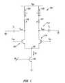
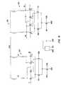
- FIG. 1is a schematic diagram of differential pair including inductive broadbanding implemented with CMOS technology
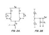
- FIG. 2( a )is a schematic diagram of the circuit of FIG. 1 without the shunt inductor
- FIG. 2( b )is a simplified diagram depicting the transient behavior of the circuit of FIG. 2( a );
- FIG. 2( c )is a graph depicting the difference between ideal and C 3 MOS step responses
- FIG. 3is a graph depicting the step response of the circuit of FIG. 1 for four values of series inductance
- FIG. 4( a )is a graph depicting inter-symbol interference (ISI) vs input pulse width for five values of series inductance;
- FIG. 4( b )is a graph depicting the output signal of the circuit of FIG. 1 with and without inductors;
- FIG. 5shows a block diagram for a circuit that combines C 3 MOS with inductive broadbanding, C 3 MOS, and conventional CMOS logic on a single silicon substrate to achieve optimum tradeoff between speed and power consumption;
- FIG. 6( a )is a schematic diagram of a serializer circuit utilizing features of the invention.
- FIG. 6( b )is a more detailed depiction of the 2:1 MUX depicted in FIG. 6( a );
- FIG. 7is a circuit diagram of a MUX utilizing features of the present invention.
- FIG. 8is a circuit diagram of a flip-flop utilizing features of the invention.
- FIG. 9is a simplified block diagram of a transceiver system that utilizes the C 3 MOS with inductive broadbanding C 3 MOS/CMOS combined logic according to the present invention to facilitate interconnecting high speed fiber optic communication channels.
- CMOS process technologyrefers generally to a variety of well established CMOS fabrication processes that form a field-effect transistor over a silicon substrate with a gate terminal typically made of polysilicon material disposed on top of an insulating material such as silicon dioxide.
- CMOS logicrefers to the use of complementary CMOS transistors (n-channel and p-channel) to form various logic gates and more complex logic circuitry, wherein zero static current is dissipated.
- the present inventionuses current-controlled mechanisms with inductive broadbanding to develop a family of very fast current-controlled CMOS (or C 3 MOSTM) with inductive broadbanding logic that can be fabricated using a variety of conventional CMOS process technologies, but that unlike conventional CMOS logic does dissipate static current.
- C 3 MOS with inductive broadbanding logic or current-controlled metal-oxide semiconductor field-effect transistor (MOSFET) logicare used herein interchangeably.
- the basic building block of this logic familyis an NMOS differential pair with series connected inductive/resistive (LR) loads.
- FIG. 1illustrates the basic C 3 MOS differential pair 200 with shunt inductors L, and load capacitors C L .
- a pair of n-channel MOSFETs 202 and 204receive differential logic signals V in + and V in ⁇ at their gate terminals, respectively.
- Resistive loads 206 and 207 in series with shunt inductors 208 and 209connect the drain terminals of MOSFETs 202 and 204 , respectively, to the power supply VDD. Drain terminals of MOSFETs 202 and 204 from the outputs V out ⁇ and V out + of the differential pair, respectively.
- the shunt inductors 208 and 209are spiral inductors coupled to the substrate utilizing standard techniques.
- Resistive loads 206 and 207may be made up of either p-channel MOSFETs operating in their linear region, or resistors made up of, for example, polysilicon material. In a preferred embodiment, polysilicon resistors are used to implement resistive loads 206 and 207 , which maximizes the speed of differential pair 200 .
- the source terminals of n-channel MOSFETs 202 and 204connect together at node 210 .
- a current-source n-channel MOSFET 212connects node 210 to ground (or negative power supply).
- a bias voltage VBdrives the gate terminal of current-source MOSFET 212 and sets up the amount of current I that flows through differential pair 200 .
- one of the two input n-channel MOSFETs 202 and 204switches on while the other switches off. All of current I, thus flows in one leg of the differential pair pulling the drain terminal (V out + or V out ⁇ ) of the on transistor down to logic low, while the drain of the other (off) transistor is pulled up toward logic high.
- Shunt peakingcan be selectively applied to those parts of an integrated circuit that require the bandwidth enhancement.
- the input levels V in + and V in ⁇vary symmetrically in opposite directions when a digital signal is received. For example if V in + swung positive then V in ⁇ would swing negative.
- the voltage levels at V out ⁇ and V out +swing in the same direction as the respective input signal levels. For reasons described more fully below, for broadband signals including frequencies in the range of over 5 GigaHz the transient response of the circuit must be fast.
- FIGS. 2( a ) and ( b )respectively depict the circuit of FIG. 1 with the inductors removed, resulting in a C 3 MOS buffer, and a simple equivalent circuit illustrating the transient behavior of the circuit.
- the output transient waveformis characterized by an exponential waveform with a time constant RC.
- This waveformis depicted in FIG. 2( c ) with a label “C 3 MOS” and has an initial slope of I/C L .
- the difference between the ideal and exponential step responseis also depicted in FIG. 2( c ).
- the transient response of the output signalwould be controlled by the RC time constant. It is clear from FIG. 2( c ) that the presence of the load resistor significantly slows down the transient step response. Thus, when an input signal is received with a very fast rise time the current increases rapidly to charge or discharge the load capacitor. However, the transient response of the output signal is controlled by the RC time constant and can have a longer rise time than the input pulse.
- FIG. 3shows the step response for 4 different values of series inductance.
- FIG. 4( b )depicts the output signals for the circuit of FIG. 1 with and without the inductors.
- the magnitude of the time intervals between zero crossing points of the output signalprovide important information for interpreting the input signal.
- the slope of the waveform zero-crossingsis sharper when the inductors are included in the circuit thereby more precisely defining the time intervals between zero-crossing points and reducing inter-symbol interference.
- a transceiver circuit along a fiber optic channeldeserializes an input data stream with a bit rate of, for example, 10 Gb/s. After processing the lower frequency deserialized data, the data is serialized before transmission back onto the fiber channel.
- this circuitrythat process the highest speed data (e.g., input to the deserializer and output of the serializer) are implemented by C 3 MOS circuitry with inductive broadbanding.
- FIG. 5shows a simplified block diagram illustrating this exemplary embodiment of the invention.
- a C 3 MOS with inductive broadbanding input circuit 40receives a high frequency input signal IN and outputs a first divided down version of the signal IN/n.
- a C 3 MOS MUX 42then receives this first divided down version and divides the received signal down by another factor of m to output a second divided down version of the signal IN/(n ⁇ m).
- the lower frequency signal IN/(n ⁇ m)is then processes by core circuitry 44 that is implemented in conventional CMOS logic.
- the low frequency signal from the core logicis then increased in frequency by the reverse process to form an output signal at the original high input frequency.
- FIG. 6( a )shows an exemplary 16:1 serializer according to the present invention.
- the serializerincludes a 16:8 multiplexer 50 that converts the data rate to 1.25 Gb/s, followed by an 8:4 multiplexer 54 that converts the data rate to 2.5 Gb/s.
- the 2.5 Gb/s datais further converted to a 5 Gb/s data by a 4:2 multiplexer 56 , and finally to a 10 Gb/s data by a 2:1 multiplexer 58 .
- a flip flop 60 at the outputre-times the 10 Gb/s data to generate the final output data stream.
- the circuit of FIG. 6( a )may combine conventional CMOS logic used for the lower speed multiplexers and core processing circuitry, with C 3 MOS logic for the mid-rate multiplexers, and C 3 MOS logic with inductive broadbanding for the highest speed multiplexer (i.e., the 2:1 multiplexer 58 ) as well as the output re-timing flip flop 60 .
- C 3 MOS with inductive broadbanding logic elementsall of the building blocks of any logic circuitry can be constructed using the C 3 MOS with inductive broadbanding technique of the present invention. More complex logic circuits such as shift registers, counters, frequency dividers, etc., can be constructed in C 3 MOS with inductive broadbanding using the basic elements described above. As mentioned above, however, both C 3 MOS and C 3 MOS with inductive broadbanding logic does consume static power. Additionally, the fabrication of C 3 MOS with inductive broadbanding logic is more expensive than C 3 MOS or CMOS because of the need to add inductors to the IC.
- the present inventioncombines C 3 MOS with inductive broadbanding and C 3 MOS logic with conventional CMOS logic to achieve an optimum balance between speed and power consumption.
- an integrated circuitutilizes C 3 MOS with inductive broadbanding logic for the ultra high speed (e.g., 10 Gb/s) portions of the circuitry, C 3 MOS for very high speed parts of the circuit (e.g., 2.5-5 Gb/s) and conventional CMOS logic for the relatively lower speed sections.
- the input and output circuitry that interfaces with and processes the high speed signalsis implemented using C 3 MOS with inductive broadbanding.
- the circuitalso employs C 3 MOS to divide down the frequency of the signals being processed to a low enough frequency where conventional CMOS logic can be used.
- the core of the circuit, according to this embodiment,is therefore implemented by conventional CMOS logic that consumes zero static current.
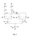
- FIG. 6( b )shows an implementation of the 2:1 multiplexer 58 wherein the actual output multiplexing circuit 62 uses C 3 MOS with inductive broadbanding an implementation of which is shown in FIG. 7 .
- FIG. 7shows an exemplary C 3 MOS with inductive broadbanding implementation for a 2:1 multiplexer 62 .
- multiplexer 62includes a differential pair for each input.
- the positive (left) input transistor of each differential pairis coupled to VDD through by a first resistor 206 connected in series with a first series inductor 208 and the negative (right) input transistor of each differential pair is coupled to VDD through by a second resistor 207 connected in series with a second series inductor 209 .
- the multiplexer 62further includes select transistors 502 and 504 inserted between the common source terminals of the differential pairs and the current source transistor 506 .
- the bias currentis steered to the differential pair associated with that select transistor.
- signal SELAsteers the bias current to the differential pair with AP and AN inputs
- signal SELBsteers the bias current to the differential pair with BP and BN inputs.
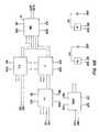
- FIG. 8shows an exemplary implementation of a C 3 MOS flip flop with inductive broadbanding for use as the re-timing flip flop in the serializer of FIG. 5 .
- a C 3 MOS master-slave flip-flop 800according to the present invention can be made by combining two latches 802 and 804 .
- a first latch 802receives differential input signals D and D and generates differential output signals QI and QI.
- the differential output signals QI and Q Iare then applied to the differential inputs of a second latch 804 .
- the differential outputs Q and Q of second latch 804provide the outputs of flip-flop 800 .
- the input transistors of each latchare coupled to VDD by a resistor and shunt inductor coupled in series.
- the combined C 3 MOS with inductive broadbanding/C 3 MOS/CMOS circuit techniqueis employed in a transceiver of the type illustrated in FIG. 9 .
- the exemplary transceiver of FIG. 9is typically found along fiber optic channels in high speed telecommunication networks.
- the transceiverincludes at its input a photo detect and driver circuit 1200 that receives the input signal from the fiber optic channel.
- Circuit 1200converts fiber-optic signal to packets of data and supplies it to a clock data recovery (CDR) circuit 1202 .
- CDR circuit 1202recovers the clock and data signals that may be in the frequency range of about 10 GHz, or higher.
- Established telecommunication standardsrequire the transceiver to perform various functions, including data monitoring and error correction.
- the transceiveruses a demultiplexer 1204 , depicted in FIGS. 5 and 6 , which deserializes the 10 Gb/s data stream into, for example, 16 parallel signals having a bit rate of about 622 Mb/s.
- An application specific integrated circuit (ASIC) 1206then performs the monitoring and error correction functions at the lower (622 Mb/s) bit rate.
- a multiplexer and clock multiplication unit (CMU) 1208converts the parallel signals back into a single bit stream at 10 Gb/s. This signal is then retransmitted back onto the fiber optic channel by a laser drive 1212 .
- the combined C 3 MOS with inductive broadbanding/C 3 MOS/CMOS technique of the present inventionallows fabrication of demultiplexer 1204 , ASIC 1206 and multiplexer and CMU 1208 on a single silicon die. That is, demultiplexer 1204 and multiplexer CMU 1208 are implemented in C 3 MOS with inductive broadbanding/C 3 MOS with ASIC 1206 implemented in conventional CMOS.
- the present inventionprovides various circuit techniques for implementing ultra high speed circuits using current-controlled CMOS (C 3 MOS) logic and C 3 MOS with inductive broadbanding logic fabricated in conventional CMOS process technology.
- the present inventionadvantageously combines high speed C 3 MOS with inductive broadbanding/C 3 MOS with inductive broadbanding/C 3 MOS logic with low power conventional CMOS logic.
- circuitssuch as transceivers along fiber optic channels can be fabricated on a single chip where the ultra-high speed portions of the circuit utilize C 3 MOS with inductive broadbanding/C 3 MOS and the relatively lower speed parts of the circuit use conventional CMOS logic.
- CMOS logicthat is based on current-controlled mechanism.
- Current-controlled CMOS (or C 3 MOS) logicis described in greater detail in commonly-assigned U.S. Utility application Ser. No. 09/484,856, entitled “Current-controlled CMOS logic family,” filed Jan. 18, 2000, now U.S. Pat. No. 6,424,194 B1, issued on Jun. 23, 2002, which is hereby incorporated in its entirety for all purposes.
- the basic building block of the C 3 MOS logic familyuses a pair of conventional MOSFETs that steer current between a pair of load devices in response to a difference between a pair of input signals.
- C 3 MOS logicdissipates static current, but operates at much higher speeds.
- the present inventionintroduces inductive elements in the C 3 MOS circuits.
- a spiral inductoris inserted in series with the load devices of selected C 3 MOS structures that process high-bandwidth data signals.
- the resulting series combination of inductor and resistive elemente.g., polysilicon resistors
- resistive elemente.g., polysilicon resistors
- Optimized values for the inductorsensure appropriate placement of the circuit's natural frequencies in the complex plane to achieve fast rise and fall times with appropriate overshoot and undershoot.
- the present inventioncombines the use of this type of shunt peaking with C 3 MOS circuits that process broadband bi-level (i.e., digital as opposed to analog) differential signals.
- the combination of these characteristicsallows for improvement of the output signal's inter-symbol interference without any increase in power dissipation.
- a multiplexer circuitincludes C 3 MOS with inductive broadbanding to facilitate operation at ultra-high frequencies.
- a flip-flopis implemented utilizing C 3 MOS with inductive broadbanding to operate at ultrahigh frequencies.
- CMOS logic circuitrycombines on the same silicon substrate, current-controlled MOSFET circuitry of the type described above for high speed signal processing, with conventional CMOS logic that does not dissipate static current.
- CMOS logicthat does not dissipate static current.
- Examples of such combined circuitryinclude serializer/deserializer circuitry used in high speed serial links, high speed phase-locked loop dividers, and the like.
Landscapes
- Engineering & Computer Science (AREA)
- Power Engineering (AREA)
- Physics & Mathematics (AREA)
- Computer Hardware Design (AREA)
- Computing Systems (AREA)
- General Engineering & Computer Science (AREA)
- Mathematical Physics (AREA)
- Logic Circuits (AREA)
- Electronic Switches (AREA)
- Control Of Electrical Variables (AREA)
- Networks Using Active Elements (AREA)
Abstract
Description
LS(opt)=(0.35)*CLR2
Claims (38)
Priority Applications (1)
| Application Number | Priority Date | Filing Date | Title |
|---|---|---|---|
| US12/368,934US7919985B2 (en) | 2000-02-24 | 2009-02-10 | Current-controlled CMOS circuits with inductive broadbanding |
Applications Claiming Priority (7)
| Application Number | Priority Date | Filing Date | Title |
|---|---|---|---|
| US18470300P | 2000-02-24 | 2000-02-24 | |
| US09/610,905US6340899B1 (en) | 2000-02-24 | 2000-07-06 | Current-controlled CMOS circuits with inductive broadbanding |
| US09/965,235US6525571B2 (en) | 2000-02-24 | 2001-09-26 | Current-controlled CMOS circuits with inductive broadbanding |
| US10/315,473US6909309B2 (en) | 2000-02-24 | 2002-12-09 | Current-controlled CMOS circuits with inductive broadbanding |
| US11/125,455US7015722B2 (en) | 2000-02-24 | 2005-05-10 | Current-controlled CMOS circuits with inductive broadbanding |
| US11/343,322US7498843B2 (en) | 2000-02-24 | 2006-01-31 | Current-controlled CMOS circuits with inductive broadbanding |
| US12/368,934US7919985B2 (en) | 2000-02-24 | 2009-02-10 | Current-controlled CMOS circuits with inductive broadbanding |
Related Parent Applications (1)
| Application Number | Title | Priority Date | Filing Date |
|---|---|---|---|
| US11/343,322ContinuationUS7498843B2 (en) | 2000-02-24 | 2006-01-31 | Current-controlled CMOS circuits with inductive broadbanding |
Publications (2)
| Publication Number | Publication Date |
|---|---|
| US20090140771A1 US20090140771A1 (en) | 2009-06-04 |
| US7919985B2true US7919985B2 (en) | 2011-04-05 |
Family
ID=26880400
Family Applications (6)
| Application Number | Title | Priority Date | Filing Date |
|---|---|---|---|
| US09/610,905Expired - LifetimeUS6340899B1 (en) | 2000-02-24 | 2000-07-06 | Current-controlled CMOS circuits with inductive broadbanding |
| US09/965,235Expired - LifetimeUS6525571B2 (en) | 2000-02-24 | 2001-09-26 | Current-controlled CMOS circuits with inductive broadbanding |
| US10/315,473Expired - LifetimeUS6909309B2 (en) | 2000-02-24 | 2002-12-09 | Current-controlled CMOS circuits with inductive broadbanding |
| US11/125,455Expired - LifetimeUS7015722B2 (en) | 2000-02-24 | 2005-05-10 | Current-controlled CMOS circuits with inductive broadbanding |
| US11/343,322Expired - Fee RelatedUS7498843B2 (en) | 2000-02-24 | 2006-01-31 | Current-controlled CMOS circuits with inductive broadbanding |
| US12/368,934Expired - Fee RelatedUS7919985B2 (en) | 2000-02-24 | 2009-02-10 | Current-controlled CMOS circuits with inductive broadbanding |
Family Applications Before (5)
| Application Number | Title | Priority Date | Filing Date |
|---|---|---|---|
| US09/610,905Expired - LifetimeUS6340899B1 (en) | 2000-02-24 | 2000-07-06 | Current-controlled CMOS circuits with inductive broadbanding |
| US09/965,235Expired - LifetimeUS6525571B2 (en) | 2000-02-24 | 2001-09-26 | Current-controlled CMOS circuits with inductive broadbanding |
| US10/315,473Expired - LifetimeUS6909309B2 (en) | 2000-02-24 | 2002-12-09 | Current-controlled CMOS circuits with inductive broadbanding |
| US11/125,455Expired - LifetimeUS7015722B2 (en) | 2000-02-24 | 2005-05-10 | Current-controlled CMOS circuits with inductive broadbanding |
| US11/343,322Expired - Fee RelatedUS7498843B2 (en) | 2000-02-24 | 2006-01-31 | Current-controlled CMOS circuits with inductive broadbanding |
Country Status (6)
| Country | Link |
|---|---|
| US (6) | US6340899B1 (en) |
| EP (1) | EP1269630B1 (en) |
| AT (1) | ATE266277T1 (en) |
| AU (1) | AU2001245332A1 (en) |
| DE (1) | DE60103142T2 (en) |
| WO (1) | WO2001063767A2 (en) |
Cited By (3)
| Publication number | Priority date | Publication date | Assignee | Title |
|---|---|---|---|---|
| US20110210767A1 (en)* | 2005-08-04 | 2011-09-01 | The Regents Of The University Of California | Phase coherent differential structures |
| US8200179B1 (en) | 2008-10-07 | 2012-06-12 | Lattice Semiconductor Corporation | Combined variable gain amplifier and analog equalizer circuit |
| US9614530B2 (en) | 2014-12-12 | 2017-04-04 | Samsung Display Co., Ltd. | Fast fall and rise time current mode logic buffer |
Families Citing this family (61)
| Publication number | Priority date | Publication date | Assignee | Title |
|---|---|---|---|---|
| US6897697B2 (en)* | 1999-06-28 | 2005-05-24 | Broadcom Corporation | Current-controlled CMOS circuit using higher voltage supply in low voltage CMOS process |
| US6909852B2 (en) | 2000-02-17 | 2005-06-21 | Broadcom Corporation | Linear full-rate phase detector and clock and data recovery circuit |
| US6847789B2 (en) | 2000-02-17 | 2005-01-25 | Broadcom Corporation | Linear half-rate phase detector and clock and data recovery circuit |
| US6340899B1 (en)* | 2000-02-24 | 2002-01-22 | Broadcom Corporation | Current-controlled CMOS circuits with inductive broadbanding |
| EP1162796B1 (en) | 2000-06-09 | 2012-08-15 | Broadcom Corporation | Cascading of gigabit switches |
| US20020149400A1 (en)* | 2001-04-16 | 2002-10-17 | Namik Kocaman | Low voltage differential to single-ended converter |
| US6614371B2 (en)* | 2001-07-19 | 2003-09-02 | Broadcom Corporation | Synchronous data serialization circuit |
| US7092474B2 (en)* | 2001-09-18 | 2006-08-15 | Broadcom Corporation | Linear phase detector for high-speed clock and data recovery |
| US6624699B2 (en)* | 2001-10-25 | 2003-09-23 | Broadcom Corporation | Current-controlled CMOS wideband data amplifier circuits |
| DE10156817C1 (en)* | 2001-11-20 | 2003-05-28 | Infineon Technologies Ag | Multi-phase comparator |
| DE10217375B4 (en) | 2002-04-18 | 2006-08-24 | Infineon Technologies Ag | Circuit arrangement and method for generating a dual-rail signal |
| US6777988B2 (en)* | 2002-04-30 | 2004-08-17 | John C. Tung | 2-level series-gated current mode logic with inductive components for high-speed circuits |
| US7127648B2 (en) | 2002-08-07 | 2006-10-24 | Broadcom Corporation | System and method for performing on-chip self-testing |
| US6650163B1 (en)* | 2002-08-08 | 2003-11-18 | International Business Machines Corporation | Clock generator for integrated circuit |
| US7111208B2 (en)* | 2002-10-02 | 2006-09-19 | Broadcom Corporation | On-chip standalone self-test system and method |
| US20040153681A1 (en)* | 2002-11-12 | 2004-08-05 | Broadcom Corporation | Phase detector for extended linear response and high-speed data regeneration |
| US6774721B1 (en) | 2003-03-07 | 2004-08-10 | Quake Technologies, Inc. | High speed logic circuits |
| JP2004304330A (en)* | 2003-03-28 | 2004-10-28 | Nec Electronics Corp | Frequency characteristics-variable amplifier circuit and semiconductor integrated circuit device |
| US7202706B1 (en) | 2003-04-10 | 2007-04-10 | Pmc-Sierra, Inc. | Systems and methods for actively-peaked current-mode logic |
| EP1471667B1 (en)* | 2003-04-22 | 2005-09-07 | Alcatel | Clock recovery from distorted optical signals |
| DE10342569A1 (en)* | 2003-09-15 | 2005-04-14 | Infineon Technologies Ag | Frequency divider for signals in gigahertz (GHZ) range, with mixer of input signal with feedback output signal, containing bandpass characteristic of mixer amplifying (MOS) transistors for working frequencies of several 10 GHz |
| US7822113B2 (en)* | 2003-12-19 | 2010-10-26 | Broadcom Corporation | Integrated decision feedback equalizer and clock and data recovery |
| US7057971B2 (en)* | 2004-01-28 | 2006-06-06 | Northop Grumman Corporation | Systems and methods that employ inductive current steering for digital logic circuits |
| US20050286641A1 (en)* | 2004-05-24 | 2005-12-29 | Jun Cao | Finite impulse response de-emphasis with inductive shunt peaking for near-end and far-end signal integrity |
| US7215194B2 (en)* | 2004-05-28 | 2007-05-08 | Cornell Research Foundation, Inc. | Extended bandwidth amplifier and oscillator using positive current feedback through inductive load |
| US20060006849A1 (en)* | 2004-06-28 | 2006-01-12 | Haslett James W | Inductor compensating circuit |
| US20060050809A1 (en)* | 2004-09-03 | 2006-03-09 | Broadcom Corporation | System and method for reducing phase distortion in a linear transmitter via the introduction of bias currents to a power amplifier |
| US7187212B1 (en)* | 2004-10-26 | 2007-03-06 | National Semiconductor Corporation | System and method for providing a fast turn on bias circuit for current mode logic transmitters |
| KR100672987B1 (en)* | 2004-12-20 | 2007-01-24 | 삼성전자주식회사 | High Speed Analog Envelope Detector |
| US7061279B1 (en)* | 2004-12-30 | 2006-06-13 | Broadcom Corporation | System and method for high frequency, high output swing buffers |
| TWI281317B (en)* | 2005-03-07 | 2007-05-11 | Sunplus Technology Co Ltd | Self DC-bias high frequency logic gate, NAND gate, and NOR gate using the same |
| US20060244519A1 (en)* | 2005-04-27 | 2006-11-02 | Broadcom Corporation | Digitally controlled uniform step size CTF |
| US7598811B2 (en) | 2005-07-29 | 2009-10-06 | Broadcom Corporation | Current-controlled CMOS (C3MOS) fully differential integrated wideband amplifier/equalizer with adjustable gain and frequency response without additional power or loading |
| US7362174B2 (en) | 2005-07-29 | 2008-04-22 | Broadcom Corporation | Current-controlled CMOS (C3MOS) wideband input data amplifier for reduced differential and common-mode reflection |
| US7598788B2 (en) | 2005-09-06 | 2009-10-06 | Broadcom Corporation | Current-controlled CMOS (C3MOS) fully differential integrated delay cell with variable delay and high bandwidth |
| JP2007173971A (en)* | 2005-12-19 | 2007-07-05 | Toyota Industries Corp | Analog frequency divider |
| US20070139079A1 (en)* | 2005-12-20 | 2007-06-21 | Tang George C | Reducing power noise in differential drivers |
| US7400169B2 (en)* | 2006-08-22 | 2008-07-15 | Broadcom Corporation | Inductor-tuned buffer circuit with improved modeling and design |
| TWI332760B (en)* | 2006-12-12 | 2010-11-01 | Realtek Semiconductor Corp | Latch |
| US7884658B2 (en)* | 2007-03-30 | 2011-02-08 | The Trustees Of Columbia University In The City Of New York | Circuits for forming the inputs of a latch |
| KR100951567B1 (en)* | 2008-02-29 | 2010-04-09 | 주식회사 하이닉스반도체 | Semiconductor memory device to ensure the reliability of data transfer |
| KR100929835B1 (en)* | 2008-02-29 | 2009-12-07 | 주식회사 하이닉스반도체 | Semiconductor memory device performing stable initial operation |
| US7656325B1 (en)* | 2008-07-09 | 2010-02-02 | Lsi Corporation | Serializer-deserializer (SerDes) having a predominantly digital architecture and method of deserializing data |
| US8248107B2 (en)* | 2010-03-11 | 2012-08-21 | Altera Corporation | High-speed differential comparator circuitry with accurately adjustable threshold |
| US20120057606A1 (en)* | 2010-09-07 | 2012-03-08 | Broadcom Corporation | Multiplexer circuit |
| US8258819B2 (en)* | 2010-10-25 | 2012-09-04 | Texas Instruments Incorporated | Latched comparator having isolation inductors |
| EP2456152B1 (en)* | 2010-11-17 | 2017-01-11 | Nxp B.V. | Integrated circuit for emulating a resistor |
| US8456202B2 (en)* | 2011-02-15 | 2013-06-04 | Texas Instruments Incorporated | Latch divider |
| US8451058B2 (en)* | 2011-06-22 | 2013-05-28 | Broadcom Corporation | Amplifier bandwidth extension for high-speed tranceivers |
| CN104054267A (en)* | 2011-09-23 | 2014-09-17 | 张量通讯公司 | High performance divider using feed forward, clock amplification and series peaking inductors |
| US8680899B2 (en)* | 2011-09-23 | 2014-03-25 | Tensorcom, Inc. | High performance divider using feed forward, clock amplification and series peaking inductors |
| JP2013085163A (en)* | 2011-10-12 | 2013-05-09 | Nippon Telegr & Teleph Corp <Ntt> | High speed input interface circuit |
| US8803609B2 (en) | 2012-05-10 | 2014-08-12 | Fujitsu Limited | Bandwidth extension of an amplifier |
| US8890566B2 (en)* | 2012-09-27 | 2014-11-18 | Semtech Corporation | Low-voltage, high-speed, current-mode latch with inductor tail and common-mode feedback for amplitude and current control |
| JP2015019134A (en)* | 2013-07-09 | 2015-01-29 | 日本電信電話株式会社 | Output circuit and transmission / reception circuit |
| US9413140B2 (en)* | 2013-12-19 | 2016-08-09 | Taiwan Semiconductor Manufacturing Company Limited | Semiconductor arrangement and formation thereof |
| US10122348B2 (en)* | 2016-03-30 | 2018-11-06 | Futurewei Technologies, Inc. | Interference-immunized multiplexer |
| US10833643B1 (en)* | 2018-12-21 | 2020-11-10 | Inphi Corporation | Method and structure for controlling bandwidth and peaking over gain in a variable gain amplifier (VGA) |
| KR102624454B1 (en) | 2019-04-05 | 2024-01-11 | 에스케이하이닉스 주식회사 | Data serializer circuit |
| US10840907B1 (en) | 2019-11-19 | 2020-11-17 | Honeywell International Inc. | Source-coupled logic with reference controlled inputs |
| US12438542B2 (en) | 2023-04-28 | 2025-10-07 | Avago Technologies International Sales Pte. Limited | Wide frequency range high speed clock multiplexer |
Citations (167)
| Publication number | Priority date | Publication date | Assignee | Title |
|---|---|---|---|---|
| US4333020A (en) | 1979-05-23 | 1982-06-01 | Motorola, Inc. | MOS Latch circuit |
| US4395774A (en) | 1981-01-12 | 1983-07-26 | National Semiconductor Corporation | Low power CMOS frequency divider |
| US4449248A (en) | 1982-02-01 | 1984-05-15 | General Electric Company | Battery saving radio circuit and system |
| US4519068A (en) | 1983-07-11 | 1985-05-21 | Motorola, Inc. | Method and apparatus for communicating variable length messages between a primary station and remote stations of a data communications system |
| US4545023A (en) | 1980-11-14 | 1985-10-01 | Engineering Project Development Limited | Hand-held computer |
| US4599526A (en) | 1983-05-13 | 1986-07-08 | At&T Bell Laboratories | Clocked latching circuit |
| US4649293A (en) | 1984-11-09 | 1987-03-10 | U.S. Philips Corporation | Clocked comparator |
| US4680787A (en) | 1984-11-21 | 1987-07-14 | Motorola, Inc. | Portable radiotelephone vehicular converter and remote handset |
| US4727309A (en) | 1987-01-22 | 1988-02-23 | Intel Corporation | Current difference current source |
| US4731796A (en) | 1984-10-25 | 1988-03-15 | Stc, Plc | Multi-mode radio transceiver |
| US4737975A (en) | 1984-09-18 | 1988-04-12 | Metrofone, Inc. | Programmable system for interfacing a standard telephone set with a radio transceiver |
| US4761822A (en) | 1985-08-23 | 1988-08-02 | Libera Developments Ltd. | Burst-mode two-way radio communications system |
| US4777657A (en) | 1987-04-01 | 1988-10-11 | Iss Engineering, Inc. | Computer controlled broadband receiver |
| JPS63280517A (en) | 1987-05-13 | 1988-11-17 | Nec Corp | Logic circuit |
| US4794649A (en) | 1986-05-06 | 1988-12-27 | Nec Corporation | Radio communication system with power saving disablement prior to call handling processes |
| US4804954A (en) | 1987-04-30 | 1989-02-14 | Motorola, Inc. | Battery saving method for portable communications receivers |
| US4806796A (en) | 1988-03-28 | 1989-02-21 | Motorola, Inc. | Active load for emitter coupled logic gate |
| US4807282A (en) | 1985-12-30 | 1989-02-21 | International Business Machines Corp. | Programmable P/C compatible communications card |
| US4817054A (en) | 1985-12-04 | 1989-03-28 | Advanced Micro Devices, Inc. | High speed RAM based data serializers |
| US4817115A (en) | 1987-02-27 | 1989-03-28 | Telxon Corporation | Encoding and decoding system for electronic data communication system |
| US4850009A (en) | 1986-05-12 | 1989-07-18 | Clinicom Incorporated | Portable handheld terminal including optical bar code reader and electromagnetic transceiver means for interactive wireless communication with a base communications station |
| US4890832A (en) | 1982-10-13 | 1990-01-02 | Sharp Kabushiki Kaisha | Compact electronic apparatus with removable processing units |
| US4894792A (en) | 1988-09-30 | 1990-01-16 | Tandy Corporation | Portable computer with removable and replaceable add-on modules |
| US4916441A (en) | 1988-09-19 | 1990-04-10 | Clinicom Incorporated | Portable handheld terminal |
| US4964121A (en) | 1989-08-30 | 1990-10-16 | Motorola, Inc. | Battery saver for a TDM system |
| US4969206A (en) | 1989-07-18 | 1990-11-06 | Phyle Industries Limited | Portable data collection device with RF transmission |
| US4970406A (en) | 1987-12-30 | 1990-11-13 | Gazelle Microcircuits, Inc. | Resettable latch circuit |
| US4977611A (en) | 1987-02-20 | 1990-12-11 | Nec Corporation | Portable radio apparatus having battery saved channel scanning function |
| US4995099A (en) | 1988-12-01 | 1991-02-19 | Motorola, Inc. | Power conservation method and apparatus for a portion of a predetermined signal |
| US5008879A (en) | 1988-11-14 | 1991-04-16 | Datapoint Corporation | LAN with interoperative multiple operational capabilities |
| US5025486A (en) | 1988-12-09 | 1991-06-18 | Dallas Semiconductor Corporation | Wireless communication system with parallel polling |
| US5029183A (en) | 1989-06-29 | 1991-07-02 | Symbol Technologies, Inc. | Packet data communication network |
| US5031231A (en) | 1988-09-26 | 1991-07-09 | Nec Corporation | Mobile telephone station with power saving circuit |
| US5033109A (en) | 1988-07-01 | 1991-07-16 | Mitsubishi Denki Kabushiki Kaisha | Pocket transceiver |
| US5041740A (en) | 1990-04-30 | 1991-08-20 | Motorola, Inc. | Parallel clocked latch |
| US5055659A (en) | 1990-02-06 | 1991-10-08 | Amtech Technology Corp. | High speed system for reading and writing data from and into remote tags |
| US5055660A (en) | 1988-06-16 | 1991-10-08 | Avicom International, Inc. | Portable transaction monitoring unit for transaction monitoring and security control systems |
| US5079452A (en) | 1990-06-29 | 1992-01-07 | Digital Equipment Corporation | High speed ECL latch with clock enable |
| US5081402A (en) | 1991-02-22 | 1992-01-14 | Comfortex Corporation | Low power consumption wireless data transmission and control system |
| US5087099A (en) | 1988-09-02 | 1992-02-11 | Stolar, Inc. | Long range multiple point wireless control and monitoring system |
| US5115151A (en) | 1990-06-08 | 1992-05-19 | Western Digital Corporation | Triple comparator circuit |
| US5117501A (en) | 1988-08-08 | 1992-05-26 | General Electric Company | Dynamic regrouping in a trunked radio communications system |
| US5119502A (en) | 1990-08-30 | 1992-06-02 | Telefonaktiebolaget L M Ericsson | Periodic system ordered rescan in a cellular communication system |
| US5121408A (en) | 1989-10-16 | 1992-06-09 | Hughes Aircraft Company | Synchronization for entry to a network in a frequency hopping communication system |
| US5123029A (en) | 1991-06-21 | 1992-06-16 | International Business Machines Corporation | Broadcast-initiated bipartite frame multi-access protocol |
| US5128938A (en) | 1989-03-03 | 1992-07-07 | Motorola, Inc. | Energy saving protocol for a communication system |
| US5134347A (en) | 1991-02-22 | 1992-07-28 | Comfortex Corporation | Low power consumption wireless data transmission and control system |
| US5142573A (en) | 1990-02-08 | 1992-08-25 | Oki Electric Industry Co., Ltd. | Telephone apparatus for radio communication with an adaptor |
| US5150361A (en) | 1989-01-23 | 1992-09-22 | Motorola, Inc. | Energy saving protocol for a TDM radio |
| US5152006A (en) | 1991-02-25 | 1992-09-29 | Motorola, Inc. | Receiver controller method and apparatus |
| US5153878A (en) | 1989-12-11 | 1992-10-06 | Motorola Inc. | Radio data communications system with diverse signaling capability |
| US5175870A (en) | 1988-12-23 | 1992-12-29 | U.S. Philips Corporation | Power economising in multiple user radio systems |
| US5177378A (en) | 1990-05-08 | 1993-01-05 | Kabushiki Kaisha Toshiba | Source-coupled FET logic circuit |
| US5179721A (en) | 1990-11-05 | 1993-01-12 | Motorola Inc. | Method for inter operation of a cellular communication system and a trunking communication system |
| US5181200A (en) | 1990-10-29 | 1993-01-19 | International Business Machines Corporation | Handoff method and apparatus for mobile wireless workstation |
| US5196805A (en) | 1992-01-31 | 1993-03-23 | Motorola, Inc. | Distributed differential amplifier arrangement |
| US5216295A (en) | 1991-08-30 | 1993-06-01 | General Instrument Corp. | Current mode logic circuits employing IGFETS |
| US5230084A (en) | 1990-12-06 | 1993-07-20 | Motorola, Inc. | Selective call receiver having extended battery saving capability |
| US5239662A (en) | 1986-09-15 | 1993-08-24 | Norand Corporation | System including multiple device communications controller which coverts data received from two different customer transaction devices each using different communications protocols into a single communications protocol |
| US5241691A (en) | 1990-03-09 | 1993-08-31 | U.S. Philips Corporation | Method of optimizing the transmission of idle beacon messages and a communications system using the method |
| US5241542A (en) | 1991-08-23 | 1993-08-31 | International Business Machines Corporation | Battery efficient operation of scheduled access protocol |
| US5247656A (en) | 1989-06-01 | 1993-09-21 | Matsushita Electric Industrial Co., Ltd. | Method and apparatus for controlling a clock signal |
| US5249302A (en) | 1987-10-09 | 1993-09-28 | Motorola, Inc. | Mixed-mode transceiver system |
| US5249220A (en) | 1991-04-18 | 1993-09-28 | Rts Electronics, Inc. | Handheld facsimile and alphanumeric message transceiver operating over telephone or wireless networks |
| US5265270A (en) | 1990-10-31 | 1993-11-23 | Motorola, Inc. | Method and apparatus for providing power conservation in a communication system |
| US5265238A (en) | 1991-01-25 | 1993-11-23 | International Business Machines Corporation | Automatic device configuration for dockable portable computers |
| US5274666A (en) | 1991-10-16 | 1993-12-28 | Telephonics Corporation | Wireless communication system |
| US5276680A (en) | 1991-04-11 | 1994-01-04 | Telesystems Slw Inc. | Wireless coupling of devices to wired network |
| US5278831A (en) | 1991-07-09 | 1994-01-11 | U.S. Philips Corporation | Information transmission system |
| US5289469A (en) | 1991-01-17 | 1994-02-22 | Kabushiki Kaisha Toshiba | Communication control unit with lower layer protocol control and higher layer protocol control |
| US5289055A (en) | 1992-11-17 | 1994-02-22 | At&T Bell Laboratories | Digital ECL bipolar logic gates suitable for low-voltage operation |
| US5291516A (en) | 1991-05-13 | 1994-03-01 | Omnipoint Data Company, Inc. | Dual mode transmitter and receiver |
| US5293639A (en) | 1991-08-09 | 1994-03-08 | Motorola, Inc. | Reduction of power consumption in a portable communication unit |
| US5297144A (en) | 1991-01-22 | 1994-03-22 | Spectrix Corporation | Reservation-based polling protocol for a wireless data communications network |
| US5296849A (en) | 1990-10-25 | 1994-03-22 | Nec Corporation | Pager receiver for enabling to omit power-on signal for receiving synchronization code in pager signal |
| US5301196A (en) | 1992-03-16 | 1994-04-05 | International Business Machines Corporation | Half-speed clock recovery and demultiplexer circuit |
| US5319369A (en) | 1992-07-20 | 1994-06-07 | France Telecom | Parallel-to-serial converter |
| US5323392A (en) | 1991-03-13 | 1994-06-21 | International Business Machines Corporation | Adaptation device and method for efficient interconnection of data processing devices and networks |
| US5331509A (en) | 1992-06-29 | 1994-07-19 | Cordata, Inc. | Modular notebook computer having a planar array of module bays and a pivotally attached flat-panel display |
| US5345449A (en) | 1989-07-07 | 1994-09-06 | Inmos Limited | Clock generation |
| US5349649A (en) | 1991-04-22 | 1994-09-20 | Kabushiki Kaisha Toshiba | Portable electronic device supporting multi-protocols |
| US5361397A (en) | 1991-08-26 | 1994-11-01 | Motorola, Inc. | Communication device and system capable of automatic programmable energizing |
| US5363121A (en) | 1990-06-29 | 1994-11-08 | International Business Machines Corporation | Multiple protocol communication interface for distributed transaction processing |
| US5373149A (en) | 1993-02-01 | 1994-12-13 | At&T Bell Laboratories | Folding electronic card assembly |
| US5373506A (en) | 1990-11-26 | 1994-12-13 | Motorola Inc. | Method and apparatus for paging in a communication system |
| US5390206A (en) | 1991-10-01 | 1995-02-14 | American Standard Inc. | Wireless communication system for air distribution system |
| US5392023A (en) | 1991-09-06 | 1995-02-21 | Motorola, Inc. | Data communication system with automatic power control |
| US5406615A (en) | 1993-08-04 | 1995-04-11 | At&T Corp. | Multi-band wireless radiotelephone operative in a plurality of air interface of differing wireless communications systems |
| US5406643A (en) | 1993-02-11 | 1995-04-11 | Motorola, Inc. | Method and apparatus for selecting between a plurality of communication paths |
| US5418837A (en) | 1993-07-30 | 1995-05-23 | Ericsson-Ge Mobile Communications Inc. | Method and apparatus for upgrading cellular mobile telephones |
| US5420529A (en) | 1994-05-19 | 1995-05-30 | Northern Telecom Limited | Current steering switch and hybrid BiCMOS multiplexer with CMOS commutation signal and CML/ECL data signals |
| US5423002A (en) | 1992-04-20 | 1995-06-06 | 3Com Corporation | System for extending network resources to remote networks |
| US5426637A (en) | 1992-12-14 | 1995-06-20 | International Business Machines Corporation | Methods and apparatus for interconnecting local area networks with wide area backbone networks |
| US5428636A (en) | 1993-05-03 | 1995-06-27 | Norand Corporation | Radio frequency local area network |
| US5430845A (en) | 1990-06-07 | 1995-07-04 | Unisys Corporation | Peripheral device interface for dynamically selecting boot disk device driver |
| US5434518A (en) | 1992-10-02 | 1995-07-18 | National Semiconductor Corporation | ECL-to-BICOMS/CMOS translator |
| US5438329A (en) | 1993-06-04 | 1995-08-01 | M & Fc Holding Company, Inc. | Duplex bi-directional multi-mode remote instrument reading and telemetry system |
| US5440560A (en) | 1991-12-24 | 1995-08-08 | Rypinski; Chandos A. | Sleep mode and contention resolution within a common channel medium access method |
| US5457412A (en) | 1992-11-17 | 1995-10-10 | Hitachi, Ltd. | Semiconductor integrated circuit device including input circuitry to permit operation of a Bi-CMOS memory with ECL level input signals |
| US5459412A (en) | 1993-07-01 | 1995-10-17 | National Semiconductor Corporation | BiCMOS circuit for translation of ECL logic levels to MOS logic levels |
| US5465081A (en) | 1990-03-03 | 1995-11-07 | Cedar-Dell Limited | Multicomponent wireless system with periodic shutdown of transmitting and receiving modes |
| EP0685933A1 (en) | 1994-06-02 | 1995-12-06 | Mitsubishi Denki Kabushiki Kaisha | Differential amplifier |
| US5481265A (en) | 1989-11-22 | 1996-01-02 | Russell; David C. | Ergonomic customizeable user/computer interface devices |
| US5481562A (en) | 1989-11-03 | 1996-01-02 | Microcom Systems, Inc. | Multi-mode modem and data transmission method |
| US5488319A (en) | 1994-08-18 | 1996-01-30 | International Business Machines Corporation | Latch interface for self-reset logic |
| US5510748A (en) | 1994-01-18 | 1996-04-23 | Vivid Semiconductor, Inc. | Integrated circuit having different power supplies for increased output voltage range while retaining small device geometries |
| US5510734A (en) | 1994-06-14 | 1996-04-23 | Nec Corporation | High speed comparator having two differential amplifier stages and latch stage |
| US5521530A (en) | 1994-08-31 | 1996-05-28 | Oki Semiconductor America, Inc. | Efficient method and resulting structure for integrated circuits with flexible I/O interface and power supply voltages |
| US5533029A (en) | 1993-11-12 | 1996-07-02 | Pacific Communication Sciences, Inc. | Cellular digital packet data mobile data base station |
| US5535373A (en) | 1991-11-27 | 1996-07-09 | International Business Machines Corporation | Protocol-to-protocol translator for interfacing disparate serial network nodes to a common parallel switching network |
| US5548230A (en) | 1994-05-31 | 1996-08-20 | Pmc-Sierra, Inc. | High-speed CMOS pseudo-ECL output driver |
| US5576644A (en) | 1994-06-10 | 1996-11-19 | International Business Machines Corporation | Fast edge triggered self-resetting CMOS receiver with parallel L1/L2 (master/slave) latch |
| US5579487A (en) | 1992-10-02 | 1996-11-26 | Teletransaction, Inc. | Portable work slate computer with multiple docking positions for interchangeably receiving removable modules |
| US5584048A (en) | 1990-08-17 | 1996-12-10 | Motorola, Inc. | Beacon based packet radio standby energy saver |
| US5600267A (en) | 1994-06-24 | 1997-02-04 | Cypress Semiconductor Corporation | Apparatus for a programmable CML to CMOS translator for power/speed adjustment |
| US5606268A (en) | 1993-03-24 | 1997-02-25 | Apple Computer, Inc. | Differential to single-ended CMOS converter |
| US5625308A (en) | 1995-06-08 | 1997-04-29 | Mitsubishi Denki Kabushiki Kaisha | Two input-two output differential latch circuit |
| US5628055A (en) | 1993-03-04 | 1997-05-06 | Telefonaktiebolaget L M Ericsson Publ | Modular radio communications system |
| US5630061A (en) | 1993-04-19 | 1997-05-13 | International Business Machines Corporation | System for enabling first computer to communicate over switched network with second computer located within LAN by using media access control driver in different modes |
| US5640356A (en) | 1995-12-29 | 1997-06-17 | Cypress Semiconductor Corp. | Two-stage differential sense amplifier with positive feedback in the first and second stages |
| US5675584A (en) | 1994-06-06 | 1997-10-07 | Sun Microsystems, Inc. | High speed serial link for fully duplexed data communication |
| US5680633A (en) | 1990-01-18 | 1997-10-21 | Norand Corporation | Modular, portable data processing terminal for use in a radio frequency communication network |
| US5724361A (en) | 1996-03-12 | 1998-03-03 | Lsi Logic Corporation | High performance n:1 multiplexer with overlap control of multi-phase clocks |
| US5726613A (en)* | 1995-02-01 | 1998-03-10 | Nippon Telegraph And Telephone Corporation | Active inductor |
| US5732346A (en) | 1993-06-17 | 1998-03-24 | Research In Motion Limited | Translation and connection device for radio frequency point of sale transaction systems |
| US5740366A (en) | 1991-10-01 | 1998-04-14 | Norand Corporation | Communication network having a plurality of bridging nodes which transmit a beacon to terminal nodes in power saving state that it has messages awaiting delivery |
| US5744366A (en) | 1992-05-01 | 1998-04-28 | Trustees Of The University Of Pennsylvania | Mesoscale devices and methods for analysis of motile cells |
| US5767699A (en) | 1996-05-28 | 1998-06-16 | Sun Microsystems, Inc. | Fully complementary differential output driver for high speed digital communications |
| US5796727A (en) | 1993-04-30 | 1998-08-18 | International Business Machines Corporation | Wide-area wireless lan access |
| US5798658A (en) | 1995-06-15 | 1998-08-25 | Werking; Paul M. | Source-coupled logic with reference controlled inputs |
| US5821809A (en) | 1996-05-23 | 1998-10-13 | International Business Machines Corporation | CMOS high-speed differential to single-ended converter circuit |
| US5839051A (en) | 1989-03-17 | 1998-11-17 | Technophone Limited | Host radio telephone to directly access a handset NAM through a connecter without requiring the handset controller to be employed |
| US5859669A (en) | 1996-11-26 | 1999-01-12 | Texas Instruments Incorporated | System for encoding an image control signal onto a pixel clock signal |
| US5877642A (en) | 1995-11-17 | 1999-03-02 | Nec Corporation | Latch circuit for receiving small amplitude signals |
| US5892382A (en) | 1997-03-25 | 1999-04-06 | Mitsubishi Denki Kabushiki Kaisha | Current mode logic circuit, source follower circuit and flip flop circuit |
| US5903176A (en) | 1996-09-04 | 1999-05-11 | Litton Systems, Inc. | Clock circuit for generating a high resolution output from a low resolution clock |
| US5905386A (en) | 1996-01-02 | 1999-05-18 | Pmc-Sierra Ltd. | CMOS SONET/ATM receiver suitable for use with pseudo ECL and TTL signaling environments |
| US5936475A (en) | 1996-06-11 | 1999-08-10 | Tchamov; Nikolay | High-speed ring oscillator |
| US5940771A (en) | 1991-05-13 | 1999-08-17 | Norand Corporation | Network supporting roaming, sleeping terminals |
| US5945847A (en) | 1997-05-20 | 1999-08-31 | Lucent Technologies | Distributed amplifier logic designs |
| US5945863A (en) | 1997-06-18 | 1999-08-31 | Applied Micro Circuits Corporation | Analog delay circuit |
| US5945858A (en) | 1997-03-31 | 1999-08-31 | Nec Corporation | Clocked flip flop circuit with built-in clock controller and frequency divider using the same |
| US5969556A (en) | 1997-03-05 | 1999-10-19 | Mitsubishi Denki Kabushiki Kaisha | Flip-flop circuit, parallel-serial converting circuit, and latch circuit |
| US6002279A (en) | 1997-10-24 | 1999-12-14 | G2 Networks, Inc. | Clock recovery circuit |
| US6014705A (en) | 1991-10-01 | 2000-01-11 | Intermec Ip Corp. | Modular portable data processing terminal having a higher layer and lower layer partitioned communication protocol stack for use in a radio frequency communications network |
| US6014041A (en) | 1997-09-26 | 2000-01-11 | Intel Corporation | Differential current switch logic gate |
| US6028454A (en) | 1997-04-11 | 2000-02-22 | The University Of Waterloo | Dynamic current mode logic family |
| US6037841A (en) | 1997-10-07 | 2000-03-14 | Applied Micro Circuits Corporation | Impedance matched CMOS transimpedance amplifier for high-speed fiber optic communications |
| US6037842A (en) | 1998-04-21 | 2000-03-14 | Applied Micro Circuits Corporation | Complementary metal-oxide semiconductor voltage controlled oscillator (CMOS VCO) |
| US6038254A (en) | 1996-06-07 | 2000-03-14 | International Business Machines Corporation | Adaptive filtering method and apparatus to compensate for a frequency difference between two clock sources |
| US6061747A (en) | 1997-10-16 | 2000-05-09 | Lsi Logic Corporation | System for sending data from-and-to a computer monitor using a high speed serial line |
| US6081162A (en) | 1999-06-17 | 2000-06-27 | Intel Corporation | Robust method and apparatus for providing a digital single-ended output from a differential input |
| US6094074A (en) | 1998-07-16 | 2000-07-25 | Seiko Epson Corporation | High speed common mode logic circuit |
| US6111425A (en) | 1998-10-15 | 2000-08-29 | International Business Machines Corporation | Very low power logic circuit family with enhanced noise immunity |
| US6114843A (en) | 1998-08-18 | 2000-09-05 | Xilinx, Inc. | Voltage down converter for multiple voltage levels |
| US6188339B1 (en) | 1998-01-23 | 2001-02-13 | Fuji Photo Film Co., Ltd. | Differential multiplexer and differential logic circuit |
| US6194950B1 (en) | 1997-08-28 | 2001-02-27 | Lucent Technologies Inc. | High-speed CMOS multiplexer |
| US6222380B1 (en) | 1998-06-15 | 2001-04-24 | International Business Machines Corporation | High speed parallel/serial link for data communication |
| US6232844B1 (en) | 1999-05-28 | 2001-05-15 | Vitesse Semiconductor Corporation | Controlled orthogonal current oscillator with ranging |
| US6259312B1 (en) | 1998-03-11 | 2001-07-10 | Nokia Mobile Phones Limited | Circuit arrangement for adjusting the impedance of a differential active component |
| US6265898B1 (en) | 1998-07-13 | 2001-07-24 | Texas Instruments Incorporated | Current mode logic gates for low-voltage high speed applications |
| US6265944B1 (en) | 1999-09-27 | 2001-07-24 | Conexant Systems, Inc. | Fully integrated broadband RF voltage amplifier with enhanced voltage gain and method |
| US6310501B1 (en) | 1998-11-27 | 2001-10-30 | Nec Corporation | Latch circuit for latching data at an edge of a clock signal |
| US6340899B1 (en) | 2000-02-24 | 2002-01-22 | Broadcom Corporation | Current-controlled CMOS circuits with inductive broadbanding |
| US6374311B1 (en) | 1991-10-01 | 2002-04-16 | Intermec Ip Corp. | Communication network having a plurality of bridging nodes which transmit a beacon to terminal nodes in power saving state that it has messages awaiting delivery |
| US6424194B1 (en) | 1999-06-28 | 2002-07-23 | Broadcom Corporation | Current-controlled CMOS logic family |
| US6463092B1 (en) | 1998-09-10 | 2002-10-08 | Silicon Image, Inc. | System and method for sending and receiving data signals over a clock signal line |
Family Cites Families (1)
| Publication number | Priority date | Publication date | Assignee | Title |
|---|---|---|---|---|
| CA1153076A (en) | 1979-12-10 | 1983-08-30 | General Electric Company | Resonator coupled differential amplifier |
- 2000
- 2000-07-06USUS09/610,905patent/US6340899B1/ennot_activeExpired - Lifetime
- 2001
- 2001-02-22WOPCT/US2001/005968patent/WO2001063767A2/enactiveIP Right Grant
- 2001-02-22EPEP01918232Apatent/EP1269630B1/ennot_activeExpired - Lifetime
- 2001-02-22ATAT01918232Tpatent/ATE266277T1/ennot_activeIP Right Cessation
- 2001-02-22DEDE60103142Tpatent/DE60103142T2/ennot_activeExpired - Lifetime
- 2001-02-22AUAU2001245332Apatent/AU2001245332A1/ennot_activeAbandoned
- 2001-09-26USUS09/965,235patent/US6525571B2/ennot_activeExpired - Lifetime
- 2002
- 2002-12-09USUS10/315,473patent/US6909309B2/ennot_activeExpired - Lifetime
- 2005
- 2005-05-10USUS11/125,455patent/US7015722B2/ennot_activeExpired - Lifetime
- 2006
- 2006-01-31USUS11/343,322patent/US7498843B2/ennot_activeExpired - Fee Related
- 2009
- 2009-02-10USUS12/368,934patent/US7919985B2/ennot_activeExpired - Fee Related
Patent Citations (177)
| Publication number | Priority date | Publication date | Assignee | Title |
|---|---|---|---|---|
| US4333020A (en) | 1979-05-23 | 1982-06-01 | Motorola, Inc. | MOS Latch circuit |
| US4545023A (en) | 1980-11-14 | 1985-10-01 | Engineering Project Development Limited | Hand-held computer |
| US4395774A (en) | 1981-01-12 | 1983-07-26 | National Semiconductor Corporation | Low power CMOS frequency divider |
| US4449248A (en) | 1982-02-01 | 1984-05-15 | General Electric Company | Battery saving radio circuit and system |
| US4890832A (en) | 1982-10-13 | 1990-01-02 | Sharp Kabushiki Kaisha | Compact electronic apparatus with removable processing units |
| US4599526A (en) | 1983-05-13 | 1986-07-08 | At&T Bell Laboratories | Clocked latching circuit |
| US4519068A (en) | 1983-07-11 | 1985-05-21 | Motorola, Inc. | Method and apparatus for communicating variable length messages between a primary station and remote stations of a data communications system |
| US4737975A (en) | 1984-09-18 | 1988-04-12 | Metrofone, Inc. | Programmable system for interfacing a standard telephone set with a radio transceiver |
| US4731796A (en) | 1984-10-25 | 1988-03-15 | Stc, Plc | Multi-mode radio transceiver |
| US4649293A (en) | 1984-11-09 | 1987-03-10 | U.S. Philips Corporation | Clocked comparator |
| US4680787A (en) | 1984-11-21 | 1987-07-14 | Motorola, Inc. | Portable radiotelephone vehicular converter and remote handset |
| US4761822A (en) | 1985-08-23 | 1988-08-02 | Libera Developments Ltd. | Burst-mode two-way radio communications system |
| US4817054A (en) | 1985-12-04 | 1989-03-28 | Advanced Micro Devices, Inc. | High speed RAM based data serializers |
| US4807282A (en) | 1985-12-30 | 1989-02-21 | International Business Machines Corp. | Programmable P/C compatible communications card |
| US4794649A (en) | 1986-05-06 | 1988-12-27 | Nec Corporation | Radio communication system with power saving disablement prior to call handling processes |
| US4850009A (en) | 1986-05-12 | 1989-07-18 | Clinicom Incorporated | Portable handheld terminal including optical bar code reader and electromagnetic transceiver means for interactive wireless communication with a base communications station |
| US5239662A (en) | 1986-09-15 | 1993-08-24 | Norand Corporation | System including multiple device communications controller which coverts data received from two different customer transaction devices each using different communications protocols into a single communications protocol |
| US4727309A (en) | 1987-01-22 | 1988-02-23 | Intel Corporation | Current difference current source |
| US4977611A (en) | 1987-02-20 | 1990-12-11 | Nec Corporation | Portable radio apparatus having battery saved channel scanning function |
| US4817115A (en) | 1987-02-27 | 1989-03-28 | Telxon Corporation | Encoding and decoding system for electronic data communication system |
| US4777657A (en) | 1987-04-01 | 1988-10-11 | Iss Engineering, Inc. | Computer controlled broadband receiver |
| US4804954A (en) | 1987-04-30 | 1989-02-14 | Motorola, Inc. | Battery saving method for portable communications receivers |
| JPS63280517A (en) | 1987-05-13 | 1988-11-17 | Nec Corp | Logic circuit |
| US5249302A (en) | 1987-10-09 | 1993-09-28 | Motorola, Inc. | Mixed-mode transceiver system |
| US4970406A (en) | 1987-12-30 | 1990-11-13 | Gazelle Microcircuits, Inc. | Resettable latch circuit |
| US4806796A (en) | 1988-03-28 | 1989-02-21 | Motorola, Inc. | Active load for emitter coupled logic gate |
| US5055660A (en) | 1988-06-16 | 1991-10-08 | Avicom International, Inc. | Portable transaction monitoring unit for transaction monitoring and security control systems |
| US5033109A (en) | 1988-07-01 | 1991-07-16 | Mitsubishi Denki Kabushiki Kaisha | Pocket transceiver |
| US5117501A (en) | 1988-08-08 | 1992-05-26 | General Electric Company | Dynamic regrouping in a trunked radio communications system |
| US5087099A (en) | 1988-09-02 | 1992-02-11 | Stolar, Inc. | Long range multiple point wireless control and monitoring system |
| US4916441A (en) | 1988-09-19 | 1990-04-10 | Clinicom Incorporated | Portable handheld terminal |
| US5031231A (en) | 1988-09-26 | 1991-07-09 | Nec Corporation | Mobile telephone station with power saving circuit |
| US4894792A (en) | 1988-09-30 | 1990-01-16 | Tandy Corporation | Portable computer with removable and replaceable add-on modules |
| US5008879A (en) | 1988-11-14 | 1991-04-16 | Datapoint Corporation | LAN with interoperative multiple operational capabilities |
| US5008879B1 (en) | 1988-11-14 | 2000-05-30 | Datapoint Corp | Lan with interoperative multiple operational capabilities |
| US4995099A (en) | 1988-12-01 | 1991-02-19 | Motorola, Inc. | Power conservation method and apparatus for a portion of a predetermined signal |
| US5025486A (en) | 1988-12-09 | 1991-06-18 | Dallas Semiconductor Corporation | Wireless communication system with parallel polling |
| US5175870A (en) | 1988-12-23 | 1992-12-29 | U.S. Philips Corporation | Power economising in multiple user radio systems |
| US5150361A (en) | 1989-01-23 | 1992-09-22 | Motorola, Inc. | Energy saving protocol for a TDM radio |
| US5128938A (en) | 1989-03-03 | 1992-07-07 | Motorola, Inc. | Energy saving protocol for a communication system |
| US5839051A (en) | 1989-03-17 | 1998-11-17 | Technophone Limited | Host radio telephone to directly access a handset NAM through a connecter without requiring the handset controller to be employed |
| US5247656A (en) | 1989-06-01 | 1993-09-21 | Matsushita Electric Industrial Co., Ltd. | Method and apparatus for controlling a clock signal |
| US5029183A (en) | 1989-06-29 | 1991-07-02 | Symbol Technologies, Inc. | Packet data communication network |
| US5345449A (en) | 1989-07-07 | 1994-09-06 | Inmos Limited | Clock generation |
| US4969206A (en) | 1989-07-18 | 1990-11-06 | Phyle Industries Limited | Portable data collection device with RF transmission |
| US4964121A (en) | 1989-08-30 | 1990-10-16 | Motorola, Inc. | Battery saver for a TDM system |
| US5121408A (en) | 1989-10-16 | 1992-06-09 | Hughes Aircraft Company | Synchronization for entry to a network in a frequency hopping communication system |
| US5481562A (en) | 1989-11-03 | 1996-01-02 | Microcom Systems, Inc. | Multi-mode modem and data transmission method |
| US5481265A (en) | 1989-11-22 | 1996-01-02 | Russell; David C. | Ergonomic customizeable user/computer interface devices |
| US5153878A (en) | 1989-12-11 | 1992-10-06 | Motorola Inc. | Radio data communications system with diverse signaling capability |
| US5680633A (en) | 1990-01-18 | 1997-10-21 | Norand Corporation | Modular, portable data processing terminal for use in a radio frequency communication network |
| US5055659A (en) | 1990-02-06 | 1991-10-08 | Amtech Technology Corp. | High speed system for reading and writing data from and into remote tags |
| US5142573A (en) | 1990-02-08 | 1992-08-25 | Oki Electric Industry Co., Ltd. | Telephone apparatus for radio communication with an adaptor |
| US5465081A (en) | 1990-03-03 | 1995-11-07 | Cedar-Dell Limited | Multicomponent wireless system with periodic shutdown of transmitting and receiving modes |
| US5241691A (en) | 1990-03-09 | 1993-08-31 | U.S. Philips Corporation | Method of optimizing the transmission of idle beacon messages and a communications system using the method |
| US5041740A (en) | 1990-04-30 | 1991-08-20 | Motorola, Inc. | Parallel clocked latch |
| US5177378A (en) | 1990-05-08 | 1993-01-05 | Kabushiki Kaisha Toshiba | Source-coupled FET logic circuit |
| US5430845A (en) | 1990-06-07 | 1995-07-04 | Unisys Corporation | Peripheral device interface for dynamically selecting boot disk device driver |
| US5115151A (en) | 1990-06-08 | 1992-05-19 | Western Digital Corporation | Triple comparator circuit |
| US5363121A (en) | 1990-06-29 | 1994-11-08 | International Business Machines Corporation | Multiple protocol communication interface for distributed transaction processing |
| US5079452A (en) | 1990-06-29 | 1992-01-07 | Digital Equipment Corporation | High speed ECL latch with clock enable |
| US5584048A (en) | 1990-08-17 | 1996-12-10 | Motorola, Inc. | Beacon based packet radio standby energy saver |
| US5119502A (en) | 1990-08-30 | 1992-06-02 | Telefonaktiebolaget L M Ericsson | Periodic system ordered rescan in a cellular communication system |
| US5296849A (en) | 1990-10-25 | 1994-03-22 | Nec Corporation | Pager receiver for enabling to omit power-on signal for receiving synchronization code in pager signal |
| US5181200A (en) | 1990-10-29 | 1993-01-19 | International Business Machines Corporation | Handoff method and apparatus for mobile wireless workstation |
| US5265270A (en) | 1990-10-31 | 1993-11-23 | Motorola, Inc. | Method and apparatus for providing power conservation in a communication system |
| US5179721A (en) | 1990-11-05 | 1993-01-12 | Motorola Inc. | Method for inter operation of a cellular communication system and a trunking communication system |
| US5373506A (en) | 1990-11-26 | 1994-12-13 | Motorola Inc. | Method and apparatus for paging in a communication system |
| US5230084A (en) | 1990-12-06 | 1993-07-20 | Motorola, Inc. | Selective call receiver having extended battery saving capability |
| US5289469A (en) | 1991-01-17 | 1994-02-22 | Kabushiki Kaisha Toshiba | Communication control unit with lower layer protocol control and higher layer protocol control |
| US5297144A (en) | 1991-01-22 | 1994-03-22 | Spectrix Corporation | Reservation-based polling protocol for a wireless data communications network |
| US5265238A (en) | 1991-01-25 | 1993-11-23 | International Business Machines Corporation | Automatic device configuration for dockable portable computers |
| US5134347A (en) | 1991-02-22 | 1992-07-28 | Comfortex Corporation | Low power consumption wireless data transmission and control system |
| US5081402A (en) | 1991-02-22 | 1992-01-14 | Comfortex Corporation | Low power consumption wireless data transmission and control system |
| US5152006A (en) | 1991-02-25 | 1992-09-29 | Motorola, Inc. | Receiver controller method and apparatus |
| US5323392A (en) | 1991-03-13 | 1994-06-21 | International Business Machines Corporation | Adaptation device and method for efficient interconnection of data processing devices and networks |
| US5276680A (en) | 1991-04-11 | 1994-01-04 | Telesystems Slw Inc. | Wireless coupling of devices to wired network |
| US5249220A (en) | 1991-04-18 | 1993-09-28 | Rts Electronics, Inc. | Handheld facsimile and alphanumeric message transceiver operating over telephone or wireless networks |
| US5349649A (en) | 1991-04-22 | 1994-09-20 | Kabushiki Kaisha Toshiba | Portable electronic device supporting multi-protocols |
| US5940771A (en) | 1991-05-13 | 1999-08-17 | Norand Corporation | Network supporting roaming, sleeping terminals |
| US5291516A (en) | 1991-05-13 | 1994-03-01 | Omnipoint Data Company, Inc. | Dual mode transmitter and receiver |
| US5123029A (en) | 1991-06-21 | 1992-06-16 | International Business Machines Corporation | Broadcast-initiated bipartite frame multi-access protocol |
| US5278831A (en) | 1991-07-09 | 1994-01-11 | U.S. Philips Corporation | Information transmission system |
| US5293639A (en) | 1991-08-09 | 1994-03-08 | Motorola, Inc. | Reduction of power consumption in a portable communication unit |
| US5241542A (en) | 1991-08-23 | 1993-08-31 | International Business Machines Corporation | Battery efficient operation of scheduled access protocol |
| US5361397A (en) | 1991-08-26 | 1994-11-01 | Motorola, Inc. | Communication device and system capable of automatic programmable energizing |
| US5216295A (en) | 1991-08-30 | 1993-06-01 | General Instrument Corp. | Current mode logic circuits employing IGFETS |
| US5392023A (en) | 1991-09-06 | 1995-02-21 | Motorola, Inc. | Data communication system with automatic power control |
| US6014705A (en) | 1991-10-01 | 2000-01-11 | Intermec Ip Corp. | Modular portable data processing terminal having a higher layer and lower layer partitioned communication protocol stack for use in a radio frequency communications network |
| US6374311B1 (en) | 1991-10-01 | 2002-04-16 | Intermec Ip Corp. | Communication network having a plurality of bridging nodes which transmit a beacon to terminal nodes in power saving state that it has messages awaiting delivery |
| US5390206A (en) | 1991-10-01 | 1995-02-14 | American Standard Inc. | Wireless communication system for air distribution system |
| US5740366A (en) | 1991-10-01 | 1998-04-14 | Norand Corporation | Communication network having a plurality of bridging nodes which transmit a beacon to terminal nodes in power saving state that it has messages awaiting delivery |
| US5274666A (en) | 1991-10-16 | 1993-12-28 | Telephonics Corporation | Wireless communication system |
| US5535373A (en) | 1991-11-27 | 1996-07-09 | International Business Machines Corporation | Protocol-to-protocol translator for interfacing disparate serial network nodes to a common parallel switching network |
| US5440560A (en) | 1991-12-24 | 1995-08-08 | Rypinski; Chandos A. | Sleep mode and contention resolution within a common channel medium access method |
| US5196805A (en) | 1992-01-31 | 1993-03-23 | Motorola, Inc. | Distributed differential amplifier arrangement |
| US5301196A (en) | 1992-03-16 | 1994-04-05 | International Business Machines Corporation | Half-speed clock recovery and demultiplexer circuit |
| US5423002A (en) | 1992-04-20 | 1995-06-06 | 3Com Corporation | System for extending network resources to remote networks |
| US5744366A (en) | 1992-05-01 | 1998-04-28 | Trustees Of The University Of Pennsylvania | Mesoscale devices and methods for analysis of motile cells |
| US5331509A (en) | 1992-06-29 | 1994-07-19 | Cordata, Inc. | Modular notebook computer having a planar array of module bays and a pivotally attached flat-panel display |
| US5319369A (en) | 1992-07-20 | 1994-06-07 | France Telecom | Parallel-to-serial converter |
| US5579487A (en) | 1992-10-02 | 1996-11-26 | Teletransaction, Inc. | Portable work slate computer with multiple docking positions for interchangeably receiving removable modules |
| US5434518A (en) | 1992-10-02 | 1995-07-18 | National Semiconductor Corporation | ECL-to-BICOMS/CMOS translator |
| US5457412A (en) | 1992-11-17 | 1995-10-10 | Hitachi, Ltd. | Semiconductor integrated circuit device including input circuitry to permit operation of a Bi-CMOS memory with ECL level input signals |
| US5289055A (en) | 1992-11-17 | 1994-02-22 | At&T Bell Laboratories | Digital ECL bipolar logic gates suitable for low-voltage operation |
| US5426637A (en) | 1992-12-14 | 1995-06-20 | International Business Machines Corporation | Methods and apparatus for interconnecting local area networks with wide area backbone networks |
| US5373149A (en) | 1993-02-01 | 1994-12-13 | At&T Bell Laboratories | Folding electronic card assembly |
| US5406643A (en) | 1993-02-11 | 1995-04-11 | Motorola, Inc. | Method and apparatus for selecting between a plurality of communication paths |
| US5628055A (en) | 1993-03-04 | 1997-05-06 | Telefonaktiebolaget L M Ericsson Publ | Modular radio communications system |
| US5606268A (en) | 1993-03-24 | 1997-02-25 | Apple Computer, Inc. | Differential to single-ended CMOS converter |
| US5630061A (en) | 1993-04-19 | 1997-05-13 | International Business Machines Corporation | System for enabling first computer to communicate over switched network with second computer located within LAN by using media access control driver in different modes |
| US5796727A (en) | 1993-04-30 | 1998-08-18 | International Business Machines Corporation | Wide-area wireless lan access |
| US5428636A (en) | 1993-05-03 | 1995-06-27 | Norand Corporation | Radio frequency local area network |
| US5438329A (en) | 1993-06-04 | 1995-08-01 | M & Fc Holding Company, Inc. | Duplex bi-directional multi-mode remote instrument reading and telemetry system |
| US5732346A (en) | 1993-06-17 | 1998-03-24 | Research In Motion Limited | Translation and connection device for radio frequency point of sale transaction systems |
| US5459412A (en) | 1993-07-01 | 1995-10-17 | National Semiconductor Corporation | BiCMOS circuit for translation of ECL logic levels to MOS logic levels |
| US5418837A (en) | 1993-07-30 | 1995-05-23 | Ericsson-Ge Mobile Communications Inc. | Method and apparatus for upgrading cellular mobile telephones |
| US5406615A (en) | 1993-08-04 | 1995-04-11 | At&T Corp. | Multi-band wireless radiotelephone operative in a plurality of air interface of differing wireless communications systems |
| US5533029A (en) | 1993-11-12 | 1996-07-02 | Pacific Communication Sciences, Inc. | Cellular digital packet data mobile data base station |
| US5544222A (en) | 1993-11-12 | 1996-08-06 | Pacific Communication Sciences, Inc. | Cellular digtial packet data mobile data base station |
| US5510748A (en) | 1994-01-18 | 1996-04-23 | Vivid Semiconductor, Inc. | Integrated circuit having different power supplies for increased output voltage range while retaining small device geometries |
| US5420529A (en) | 1994-05-19 | 1995-05-30 | Northern Telecom Limited | Current steering switch and hybrid BiCMOS multiplexer with CMOS commutation signal and CML/ECL data signals |
| US5548230A (en) | 1994-05-31 | 1996-08-20 | Pmc-Sierra, Inc. | High-speed CMOS pseudo-ECL output driver |
| EP0685933A1 (en) | 1994-06-02 | 1995-12-06 | Mitsubishi Denki Kabushiki Kaisha | Differential amplifier |
| EP0685933B1 (en) | 1994-06-02 | 2000-01-12 | Mitsubishi Denki Kabushiki Kaisha | Differential amplifier |
| US5675584A (en) | 1994-06-06 | 1997-10-07 | Sun Microsystems, Inc. | High speed serial link for fully duplexed data communication |
| US5576644A (en) | 1994-06-10 | 1996-11-19 | International Business Machines Corporation | Fast edge triggered self-resetting CMOS receiver with parallel L1/L2 (master/slave) latch |
| US5510734A (en) | 1994-06-14 | 1996-04-23 | Nec Corporation | High speed comparator having two differential amplifier stages and latch stage |
| US5600267A (en) | 1994-06-24 | 1997-02-04 | Cypress Semiconductor Corporation | Apparatus for a programmable CML to CMOS translator for power/speed adjustment |
| US5488319A (en) | 1994-08-18 | 1996-01-30 | International Business Machines Corporation | Latch interface for self-reset logic |
| US5521530A (en) | 1994-08-31 | 1996-05-28 | Oki Semiconductor America, Inc. | Efficient method and resulting structure for integrated circuits with flexible I/O interface and power supply voltages |
| US5726613A (en)* | 1995-02-01 | 1998-03-10 | Nippon Telegraph And Telephone Corporation | Active inductor |
| US5625308A (en) | 1995-06-08 | 1997-04-29 | Mitsubishi Denki Kabushiki Kaisha | Two input-two output differential latch circuit |
| US5798658A (en) | 1995-06-15 | 1998-08-25 | Werking; Paul M. | Source-coupled logic with reference controlled inputs |
| US5877642A (en) | 1995-11-17 | 1999-03-02 | Nec Corporation | Latch circuit for receiving small amplitude signals |
| US5640356A (en) | 1995-12-29 | 1997-06-17 | Cypress Semiconductor Corp. | Two-stage differential sense amplifier with positive feedback in the first and second stages |
| US5905386A (en) | 1996-01-02 | 1999-05-18 | Pmc-Sierra Ltd. | CMOS SONET/ATM receiver suitable for use with pseudo ECL and TTL signaling environments |
| US5724361A (en) | 1996-03-12 | 1998-03-03 | Lsi Logic Corporation | High performance n:1 multiplexer with overlap control of multi-phase clocks |
| US5726588A (en) | 1996-03-12 | 1998-03-10 | Lsi Logic Corporation | Differential-to-CMOS level converter having cross-over voltage adjustment |
| US5821809A (en) | 1996-05-23 | 1998-10-13 | International Business Machines Corporation | CMOS high-speed differential to single-ended converter circuit |
| US5767699A (en) | 1996-05-28 | 1998-06-16 | Sun Microsystems, Inc. | Fully complementary differential output driver for high speed digital communications |
| US6038254A (en) | 1996-06-07 | 2000-03-14 | International Business Machines Corporation | Adaptive filtering method and apparatus to compensate for a frequency difference between two clock sources |
| US5936475A (en) | 1996-06-11 | 1999-08-10 | Tchamov; Nikolay | High-speed ring oscillator |
| US5903176A (en) | 1996-09-04 | 1999-05-11 | Litton Systems, Inc. | Clock circuit for generating a high resolution output from a low resolution clock |
| US5859669A (en) | 1996-11-26 | 1999-01-12 | Texas Instruments Incorporated | System for encoding an image control signal onto a pixel clock signal |
| US5969556A (en) | 1997-03-05 | 1999-10-19 | Mitsubishi Denki Kabushiki Kaisha | Flip-flop circuit, parallel-serial converting circuit, and latch circuit |
| US6104214A (en) | 1997-03-25 | 2000-08-15 | Mitsubishi Denki Kabushiki Kaisha | Current mode logic circuit, source follower circuit, and flip flop circuit |
| US5892382A (en) | 1997-03-25 | 1999-04-06 | Mitsubishi Denki Kabushiki Kaisha | Current mode logic circuit, source follower circuit and flip flop circuit |
| US5945858A (en) | 1997-03-31 | 1999-08-31 | Nec Corporation | Clocked flip flop circuit with built-in clock controller and frequency divider using the same |
| US6028454A (en) | 1997-04-11 | 2000-02-22 | The University Of Waterloo | Dynamic current mode logic family |
| US5945847A (en) | 1997-05-20 | 1999-08-31 | Lucent Technologies | Distributed amplifier logic designs |
| US5945863A (en) | 1997-06-18 | 1999-08-31 | Applied Micro Circuits Corporation | Analog delay circuit |
| US6194950B1 (en) | 1997-08-28 | 2001-02-27 | Lucent Technologies Inc. | High-speed CMOS multiplexer |
| US6014041A (en) | 1997-09-26 | 2000-01-11 | Intel Corporation | Differential current switch logic gate |
| US6037841A (en) | 1997-10-07 | 2000-03-14 | Applied Micro Circuits Corporation | Impedance matched CMOS transimpedance amplifier for high-speed fiber optic communications |
| US6061747A (en) | 1997-10-16 | 2000-05-09 | Lsi Logic Corporation | System for sending data from-and-to a computer monitor using a high speed serial line |
| US6002279A (en) | 1997-10-24 | 1999-12-14 | G2 Networks, Inc. | Clock recovery circuit |
| US6188339B1 (en) | 1998-01-23 | 2001-02-13 | Fuji Photo Film Co., Ltd. | Differential multiplexer and differential logic circuit |
| US6259312B1 (en) | 1998-03-11 | 2001-07-10 | Nokia Mobile Phones Limited | Circuit arrangement for adjusting the impedance of a differential active component |
| US6037842A (en) | 1998-04-21 | 2000-03-14 | Applied Micro Circuits Corporation | Complementary metal-oxide semiconductor voltage controlled oscillator (CMOS VCO) |
| US6222380B1 (en) | 1998-06-15 | 2001-04-24 | International Business Machines Corporation | High speed parallel/serial link for data communication |
| US6265898B1 (en) | 1998-07-13 | 2001-07-24 | Texas Instruments Incorporated | Current mode logic gates for low-voltage high speed applications |
| US6094074A (en) | 1998-07-16 | 2000-07-25 | Seiko Epson Corporation | High speed common mode logic circuit |
| US6114843A (en) | 1998-08-18 | 2000-09-05 | Xilinx, Inc. | Voltage down converter for multiple voltage levels |
| US6463092B1 (en) | 1998-09-10 | 2002-10-08 | Silicon Image, Inc. | System and method for sending and receiving data signals over a clock signal line |
| US6111425A (en) | 1998-10-15 | 2000-08-29 | International Business Machines Corporation | Very low power logic circuit family with enhanced noise immunity |
| US6310501B1 (en) | 1998-11-27 | 2001-10-30 | Nec Corporation | Latch circuit for latching data at an edge of a clock signal |
| US6232844B1 (en) | 1999-05-28 | 2001-05-15 | Vitesse Semiconductor Corporation | Controlled orthogonal current oscillator with ranging |
| US6081162A (en) | 1999-06-17 | 2000-06-27 | Intel Corporation | Robust method and apparatus for providing a digital single-ended output from a differential input |
| US6424194B1 (en) | 1999-06-28 | 2002-07-23 | Broadcom Corporation | Current-controlled CMOS logic family |
| US6265944B1 (en) | 1999-09-27 | 2001-07-24 | Conexant Systems, Inc. | Fully integrated broadband RF voltage amplifier with enhanced voltage gain and method |
| US20020017921A1 (en) | 2000-02-24 | 2002-02-14 | Broadcom Corporation | Current-controlled CMOS circuits with inductive broadbanding |
| US6340899B1 (en) | 2000-02-24 | 2002-01-22 | Broadcom Corporation | Current-controlled CMOS circuits with inductive broadbanding |
| US6525571B2 (en) | 2000-02-24 | 2003-02-25 | Broadcom Corporation | Current-controlled CMOS circuits with inductive broadbanding |
| US6909309B2 (en) | 2000-02-24 | 2005-06-21 | Broadcom Corporation | Current-controlled CMOS circuits with inductive broadbanding |
| US7015722B2 (en) | 2000-02-24 | 2006-03-21 | Broadcom Corporation | Current-controlled CMOS circuits with inductive broadbanding |
| US7498843B2 (en) | 2000-02-24 | 2009-03-03 | Broadcom Corporation | Current-controlled CMOS circuits with inductive broadbanding |
Non-Patent Citations (67)
| Title |
|---|
| Atkinson, A Single Chip Radio Transceiver for DECT, IEEE 1997. |
| Bagby, "One Approach to Wireless Network Architecture," IEEE P802.11191-2, Jan. 1991, pp. 1-15, 17-21. |
| Baumert et al., A Monolithic 50-200 MHz CMOS Clock Recovery and Retiming Circuit, IEEE 1989 Custom Integrated Circuits Conference pp. 14.5.1-14.5.4, (May 1989). |
| Biba, A Modest Proposal for a Asynchronous, Data Intensive, Wireless Local Area Network, IEEE P802.11191-25, Mar. 1991; pp. 1-25. |
| Bida, "A Hybrid Wireless MAC Protocol Supporting Asynchronous and Synchronous MSDU Delivery Services," IEEE 802.11/91-92, Sep. 1991, pp. 1-46. |
| Buhanan, "CML and Flip TAB Joint Forces in the DPS 88's Micropackages," Electronics Nov. 3, 1982. |
| Cheah, "A Proposed Architecture and Access Protocol Outline for the IEEE 802.11 Radio LAN Standards," Document IEEE P802.11/91-54, May 1991; pp. 1-20. |
| Chen and Barker, A 1.25Gb/s, 460mW CMOS Transceiver for Serial Data Communication, 1997 IEEE International Solid-state Circuits Conference pp. 242-243, 465. |
| Chen and Waldron, A Single-Chip 266Mbls CMOS TransmitterlReceiver for Serial Data Communications, 1993 IEEE International Solid-State Circuits Conference Digest of Technical Papers, pp. 100-101, 269. |
| Chu et al.: "A comparison of CMOS circuit techniques: Differential cascode voltage switch logic versus conventional logic" IEEE Journal of Solid-State Circuits, vol. SC-22(4) pp. 528-532, (Aug. 1987). |
| Cox, "A Radio System Proposal for Widespread Low-Power Tetherless Communications," IEEE Transactions on Communications, vol. 39, No. 2 (Feb. 1991), pp. 324-335. |
| Djahanshahi et al., High-speed ECL-Compatible Serial I/0 in 0.35mum CMOS, IEEE 1998. |
| Djahanshahi et al., High-speed ECL-Compatible Serial I/0 in 0.35μm CMOS, IEEE 1998. |
| Dunlop et al., A 9 Gbitls Bandwidth MultiplexerfDemultiplexer CMOS Chip, 1992 Symposium on VLSI Circuits Digest of Technical Papers pp. 68-69. |
| Elrabaa et al; "Optimization of Digital BiCMOS Circuits, An Overview," IEEE 1992, 5 pages. |
| Elrabaa, Multimitter BiCMOS CML Circuits, IEEE Journal of Solid-State Circuits, vol. 27, No. 3, pp. 454-458 (Mar. 1992). |
| Elrabaa, Optimization of Digital BiCMOS Circuits, An Overview, IEEE 1992. |
| European Search Report; EP06008842.4-2215, dated Jun. 22, 2009. |
| Ewen et al., CMOS circuits for Gbls serial data communication, IBM J. Res. Develop., vol. 39 No. 12 pp. 73-81 (Mar. 1995). |
| Ewen et al., Single-Chip 1062Mbaud CMOS Transceiver for Serial Data Communication, 1995 IEEE International Solid-State Circuits Conference Digest of Technical Papers, pp. 32-33, 336. |
| Fiedler et al., A 1.0625Gbps Transceiver with 2x-Oversampling and Transmit Signal Pre-Emphasis, 1997 IEEE International Solid-state Circuits onference pp. 238-239,464. |
| Friedman et al, A Baseband Processor for IS-54 Cellular Telephony, IEEE Journal of Solid-state Circuits, vol. 31 No. 5 pp. 646-655 (May 1996). |
| Fukaishi et al., A 4.25-Gbls CMOS Fiber Channel Transceiver with Asynchronous Tree-Type Demultiplexer and Frequency Conversion Architecture, IEEE Journal of Solid-state Circuits, vol. 33 No. 12, pp. 2139-2147 (1998). |
| Gray et al., "Analysis and Design of Analog Integrated Circuits," John Wiley Sons, Inc., pp. 704-709, (1977). |
| Gray, P.R. and Meyer, R.G. "MOS amplifier design," Chapter 12 in Analysis and Design of Analog Integrated Circuits. 1977, John Wiley & Sons, Inc., New York, NY, pp. 704-709. |
| Harrold, "An Introduction to GaAs IC Design," Prentice Hall International, UK Ltd., pp. 43-45, 63, 160, (1993). |
| Harrold, S.J. "Source-coupled FET logic (SCFL) [29]," Chapter 3 In An Introduction to GaAs IC Design. 1993, Prentice Hall International, UK Ltd., Hertfordshire, Great Britain, pp. 43-45, 63, 160. |
| Heimsch, "Merged CMOSIBipolar Current Switch Logic (MCSL)," IEEE Journal of SolidState Circuits, vol. 24, No. 5, pp. 1307-1311 (Oct. 1989). |
| Heimschi et al; Merged CMOS/Bipolar Current Switch Logic (MCSL), IEEE Journal of Solid State Circuits, Oct. 1989, vol. 24, pp. 1307-1311. |
| Heller et al.: "Cascade voltage switch logic: A differential CMOS logic family", IEEE International Solid-State Circuits Conference, pp. 16-17 (Feb. 22, 1984). |
| Heller, L.G. et al. "Cascade voltage switch logic: A differential CMOS logic family," IEEE International Solid-State Circuits Conference Feb. 22, 1984, pp. 16-17. |
| Hoberecht, "A Layered network Protocol for Packet Voice and Data Integration," IEEE Journal on Selected Areas in Communications, vol. SAC-1, No. 6 (Dec. 1983), pp. 1006-1013. |
| Hodges et al., "Analysis and Design of Digital Integrated Circuits." McGraw Hill, Inc., pp. 271-283, (1983). |
| Hodges, D.A. and Jackson, H.G. "Emitter-coupled logic," Chapter 7 In Analysis and Design of Digital Integrated Circuits. 1983, McGraw Hill, Inc., New York, NY, pp. 271-283. |
| Katsu, S. et al. "A GaAs monolithic frequency divider using source coupled FET logic," IEEE Electron Device Letters Aug. 1982, pp. 197-199, vol. EDL-3, No. 8. |
| Katsu, S. et al. "A source coupled FET logic-A new current-mode approach to GaAs logics," IEEE Transactions on Electron Devices Jun. 1985, pp. 1114-1118, vol. ED-32, No. 6. |
| Klose, "Process-Optimization for Sub-30ps BiCMOS Technologies for Mixed ECLICMOS Applications," IEEE 1991. |
| Kurisu et al., 2.8Gb/s 176mW Byte-Interleaved and 3.0 Gbls 118mW Bit-Interleaved 8:1 Multiplexers, 1996 International Solid state Circuits Conference pp. 122-123, 429. |
| Lee et al., "A CMOS Serial Link for 1 Gbaud Fully Duplexed Data Communication," 1994 Symposium on VLSI Circuits Digest of Technical Papers, pp. 125-126. |
| Lee et al., A CMOS Serial Link for Fully Duplexed Data Communication, IEEE Journal of Solid-State Circuits, vol. 30, pp. 353-364 (Apr. 1995). |
| Lee, T.H. "High-frequency amplifier design," Chapter 8 In The Design of CMOS Radio-Frequency Integrated Circuits. 1998, Cambridge Press, New York, N.Y., pp. 178-185. |
| Madhavan and Levi, Low-Power 2.5 Gbitls VCSEL driver in 0.5mum CMOS technology, Electronics Letters, vol. 34 No. 2 pp. 178-179 (Jan. 1998). |
| Madhavan and Levi, Low-Power 2.5 Gbitls VCSEL driver in 0.5μm CMOS technology, Electronics Letters, vol. 34 No. 2 pp. 178-179 (Jan. 1998). |
| Mizuno, et al., "A GHZ MOS Adaptive Pipeline Technique Using MOS Current-Mode Logic," IEEE Journal of Solid-State Circuits, vol. 31, No. 6, pp. 784-791, (Jun. 1996). |
| Mizuno, M. et al. "A GHz MOS adaptive pipeline technique using MOS current-mode logic," IEEE J. of Solid-State Circuits Jun. 1996, pp. 784-791, vol. 31, No. 6. |
| Mudd et al, "Very High Speed ECLICMG Gate Arrays with Submicron Structures," IEEE 1989, 5 pages. |
| Natarajan et al, "Battery Efficient Operation of Radio MAC Protocol," IEEE P802.11191-102, Sep. 1991, pp. 1-5. |
| Navarro and Van Noije, Design of an 8:I MUX at 1.7Gbit/s in 0.8mum CMOS Technology, 1998 Great Lakes Symposium on VLSI. |
| Navarro and Van Noije, Design of an 8:I MUX at 1.7Gbit/s in 0.8μm CMOS Technology, 1998 Great Lakes Symposium on VLSI. |
| Oshima et al., "A Single CMOS SDH Terminal Chip for 622 Mbls STM 4C," 1994 IEEE International SolidState Circuits Conference Digest of Technical Papers, pp. 174-175. |
| Pederson and Metz, A CMOS to IOOK ECL Interface Circuit, 1989 IEEE International Solid-state Circuits Conference pp. 226-227, 345. |
| Pfennings, L.e.M.G. et al. "Differential split-level CMOS logic for subnanosecond speeds," IEEE Journal ofSolid State Circuits Oct. 1985, pp. 1050-1055, vol. SC-20, No. 5. |
| Quigley et al., Current Mode Transceiver Logic, (CMTL) for Reduced Swing CMOS, Chip to Chip Communication, IEEE 1993. |
| Robert Meier's Master's Thesis, Mobile Computer Network Architecture, May 1993, 82 pages. |
| Rudell, J. et al. "A 1.9-GHz wide-band IF double conversion CMOS receiver for cordless telephone applications," IEEE Journal of Solid State Circuits Dec. 1997, pp. 2071-2088, vol. 32, No. 12. |
| Runge and Thomas, 5Gbit/s 2:1 multiplexer fabricated in 0.35mum CMOS and 3Gbit/s 1:2 demultiplexer fabricated in 0.5mum CMOS technology, Electronics Letters, vol. 35 No. 19.pp. 163 1-33 (Sep. 1999). |
| Runge and Thomas, 5Gbit/s 2:1 multiplexer fabricated in 0.35μm CMOS and 3Gbit/s 1:2 demultiplexer fabricated in 0.5μm CMOS technology, Electronics Letters, vol. 35 No. 19.pp. 163 1-33 (Sep. 1999). |
| Rypinski, "Architecture-Topology and Protocol Stacks," IEEE 802.11191-21, Mar. 1991, 12 pages. |
| Rypinski, Power-Drain Considerations for Full Time and Sleep Mode Radio Receivers, IEEE P802.11/91-99, Sep. 1991, 11 pages. |
| Somasekhar, D'. and Kaushik, R. "Differential current switch logic a power DCVS logic family," IEEE Journal of Solid-State Circuits Jul. 1996, pp. 981-991, vol. 31, No. 7. |
| Thompson et al., A 300-MHz BiCMOS Serial Data Transceiver, IEEE Journal of Solid-state Circuits, vol. 29 No. 3 pp. 185-192 (1994). |
| Widmer et al., "Single-Chip 4xSOOMbaud CMOS Transceiver," 1996 IEEE International SolidState Circuits Conference Digest of Technical Papers, pp. 126-127, 430. |
| Widmer et al., Single-Chip 4x50CLMEd CMOS Transceiver, IEEE Journal of Solid-state Circuits, vol. 31 No. 12 pp. 2004-2014 (1996). |
| Yamashina et al., "A Low-Supply Voltage GHz MOS Integrated Circuit for Mobile Computing Systems," IEEE Symposium on Low Power Electronics, XP002386133, Oct. 1994, pp. 80-81. |
| Yamashina, M. and Yamada, H. "An MOS current mode logic (MCML) circuit for low-power sub-GHz processors," IEICE Trans. Electron. Oct. 1992, pp. 1181-1187, vol. E75-C, No. 10. |
| Yamashina, M. and Yamada, H. "An MOS current mode logic (MCML) circuit for low-power sub-GHz processors," NEC Res. Develop. Jan. 1995, pp. 54-63, vol. 36, No. 1. |
| Yuen et al., An ECL Gate Array with 2.5 GHz Embedded PLL, IEEE 1993. |
Cited By (4)
| Publication number | Priority date | Publication date | Assignee | Title |
|---|---|---|---|---|
| US20110210767A1 (en)* | 2005-08-04 | 2011-09-01 | The Regents Of The University Of California | Phase coherent differential structures |
| US8775984B2 (en)* | 2005-08-04 | 2014-07-08 | The Regents Of The University Of California | Phase coherent differential structures |
| US8200179B1 (en) | 2008-10-07 | 2012-06-12 | Lattice Semiconductor Corporation | Combined variable gain amplifier and analog equalizer circuit |
| US9614530B2 (en) | 2014-12-12 | 2017-04-04 | Samsung Display Co., Ltd. | Fast fall and rise time current mode logic buffer |
Also Published As
| Publication number | Publication date |
|---|---|
| US6340899B1 (en) | 2002-01-22 |
| ATE266277T1 (en) | 2004-05-15 |
| EP1269630A2 (en) | 2003-01-02 |
| AU2001245332A1 (en) | 2001-09-03 |
| WO2001063767A2 (en) | 2001-08-30 |
| WO2001063767A3 (en) | 2002-02-21 |
| US20050258873A1 (en) | 2005-11-24 |
| EP1269630B1 (en) | 2004-05-06 |
| US7015722B2 (en) | 2006-03-21 |
| US20030122603A1 (en) | 2003-07-03 |
| US20020017921A1 (en) | 2002-02-14 |
| US7498843B2 (en) | 2009-03-03 |
| DE60103142D1 (en) | 2004-06-09 |
| US20080012600A1 (en) | 2008-01-17 |
| US6909309B2 (en) | 2005-06-21 |
| US20090140771A1 (en) | 2009-06-04 |
| DE60103142T2 (en) | 2005-06-30 |
| US6525571B2 (en) | 2003-02-25 |
Similar Documents
| Publication | Publication Date | Title |
|---|---|---|
| US7919985B2 (en) | Current-controlled CMOS circuits with inductive broadbanding | |
| Heydari et al. | Design of ultrahigh-speed low-voltage CMOS CML buffers and latches | |
| US10396763B2 (en) | Current-controlled CMOS logic family | |
| US7560957B2 (en) | High-speed CML circuit design | |
| US6982583B2 (en) | Current-controlled CMOS circuit using higher voltage supply in low voltage CMOS process | |
| US6911855B2 (en) | Current-controlled CMOS circuit using higher voltage supply in low voltage CMOS process | |
| US7388406B2 (en) | CML circuit devices having improved headroom | |
| US7710159B2 (en) | Muller-c element | |
| US6788103B1 (en) | Activ shunt-peaked logic gates | |
| Steyaert et al. | ECL-CMOS and CMOS-ECL interface in 1.2-mu m CMOS for 150-MHz digital ECL data transmission systems | |
| US20030210097A1 (en) | CMOS amplifier for optoelectronic receivers | |
| Heydari | Design issues in low-voltage high-speed current-mode logic buffers | |
| Chalvatzis et al. | A 40-Gb/s decision circuit in 90-nm CMOS | |
| Mohanavelu et al. | A novel 40-GHz flip-flop-based frequency divider in 0.18/spl mu/m CMOS | |
| Sialm et al. | 40 Gbit/s limiting output buffer in 80 nm CMOS |
Legal Events
| Date | Code | Title | Description |
|---|---|---|---|
| FEPP | Fee payment procedure | Free format text:PAYOR NUMBER ASSIGNED (ORIGINAL EVENT CODE: ASPN); ENTITY STATUS OF PATENT OWNER: LARGE ENTITY | |
| STCF | Information on status: patent grant | Free format text:PATENTED CASE | |
| FPAY | Fee payment | Year of fee payment:4 | |
| SULP | Surcharge for late payment | ||
| AS | Assignment | Owner name:BANK OF AMERICA, N.A., AS COLLATERAL AGENT, NORTH CAROLINA Free format text:PATENT SECURITY AGREEMENT;ASSIGNOR:BROADCOM CORPORATION;REEL/FRAME:037806/0001 Effective date:20160201 Owner name:BANK OF AMERICA, N.A., AS COLLATERAL AGENT, NORTH Free format text:PATENT SECURITY AGREEMENT;ASSIGNOR:BROADCOM CORPORATION;REEL/FRAME:037806/0001 Effective date:20160201 | |
| AS | Assignment | Owner name:AVAGO TECHNOLOGIES GENERAL IP (SINGAPORE) PTE. LTD., SINGAPORE Free format text:ASSIGNMENT OF ASSIGNORS INTEREST;ASSIGNOR:BROADCOM CORPORATION;REEL/FRAME:041706/0001 Effective date:20170120 Owner name:AVAGO TECHNOLOGIES GENERAL IP (SINGAPORE) PTE. LTD Free format text:ASSIGNMENT OF ASSIGNORS INTEREST;ASSIGNOR:BROADCOM CORPORATION;REEL/FRAME:041706/0001 Effective date:20170120 | |
| AS | Assignment | Owner name:BROADCOM CORPORATION, CALIFORNIA Free format text:TERMINATION AND RELEASE OF SECURITY INTEREST IN PATENTS;ASSIGNOR:BANK OF AMERICA, N.A., AS COLLATERAL AGENT;REEL/FRAME:041712/0001 Effective date:20170119 | |
| AS | Assignment | Owner name:AVAGO TECHNOLOGIES INTERNATIONAL SALES PTE. LIMITE Free format text:MERGER;ASSIGNOR:AVAGO TECHNOLOGIES GENERAL IP (SINGAPORE) PTE. LTD.;REEL/FRAME:047196/0687 Effective date:20180509 | |
| MAFP | Maintenance fee payment | Free format text:PAYMENT OF MAINTENANCE FEE, 8TH YEAR, LARGE ENTITY (ORIGINAL EVENT CODE: M1552); ENTITY STATUS OF PATENT OWNER: LARGE ENTITY Year of fee payment:8 | |
| AS | Assignment | Owner name:AVAGO TECHNOLOGIES INTERNATIONAL SALES PTE. LIMITE Free format text:CORRECTIVE ASSIGNMENT TO CORRECT THE EFFECTIVE DATE OF MERGER TO 9/5/2018 PREVIOUSLY RECORDED AT REEL: 047196 FRAME: 0687. ASSIGNOR(S) HEREBY CONFIRMS THE MERGER;ASSIGNOR:AVAGO TECHNOLOGIES GENERAL IP (SINGAPORE) PTE. LTD.;REEL/FRAME:047630/0344 Effective date:20180905 | |
| AS | Assignment | Owner name:AVAGO TECHNOLOGIES INTERNATIONAL SALES PTE. LIMITE Free format text:CORRECTIVE ASSIGNMENT TO CORRECT THE PROPERTY NUMBERS PREVIOUSLY RECORDED AT REEL: 47630 FRAME: 344. ASSIGNOR(S) HEREBY CONFIRMS THE ASSIGNMENT;ASSIGNOR:AVAGO TECHNOLOGIES GENERAL IP (SINGAPORE) PTE. LTD.;REEL/FRAME:048883/0267 Effective date:20180905 | |
| FEPP | Fee payment procedure | Free format text:MAINTENANCE FEE REMINDER MAILED (ORIGINAL EVENT CODE: REM.); ENTITY STATUS OF PATENT OWNER: LARGE ENTITY | |
| LAPS | Lapse for failure to pay maintenance fees | Free format text:PATENT EXPIRED FOR FAILURE TO PAY MAINTENANCE FEES (ORIGINAL EVENT CODE: EXP.); ENTITY STATUS OF PATENT OWNER: LARGE ENTITY | |
| STCH | Information on status: patent discontinuation | Free format text:PATENT EXPIRED DUE TO NONPAYMENT OF MAINTENANCE FEES UNDER 37 CFR 1.362 | |
| FP | Lapsed due to failure to pay maintenance fee | Effective date:20230405 |