US7918938B2 - High temperature ALD inlet manifold - Google Patents
High temperature ALD inlet manifoldDownload PDFInfo
- Publication number
- US7918938B2 US7918938B2US11/654,372US65437207AUS7918938B2US 7918938 B2US7918938 B2US 7918938B2US 65437207 AUS65437207 AUS 65437207AUS 7918938 B2US7918938 B2US 7918938B2
- Authority
- US
- United States
- Prior art keywords
- reactant
- gas
- valve
- inert gas
- line
- Prior art date
- Legal status (The legal status is an assumption and is not a legal conclusion. Google has not performed a legal analysis and makes no representation as to the accuracy of the status listed.)
- Active, expires
Links
Images


Classifications
- C—CHEMISTRY; METALLURGY
- C23—COATING METALLIC MATERIAL; COATING MATERIAL WITH METALLIC MATERIAL; CHEMICAL SURFACE TREATMENT; DIFFUSION TREATMENT OF METALLIC MATERIAL; COATING BY VACUUM EVAPORATION, BY SPUTTERING, BY ION IMPLANTATION OR BY CHEMICAL VAPOUR DEPOSITION, IN GENERAL; INHIBITING CORROSION OF METALLIC MATERIAL OR INCRUSTATION IN GENERAL
- C23C—COATING METALLIC MATERIAL; COATING MATERIAL WITH METALLIC MATERIAL; SURFACE TREATMENT OF METALLIC MATERIAL BY DIFFUSION INTO THE SURFACE, BY CHEMICAL CONVERSION OR SUBSTITUTION; COATING BY VACUUM EVAPORATION, BY SPUTTERING, BY ION IMPLANTATION OR BY CHEMICAL VAPOUR DEPOSITION, IN GENERAL
- C23C16/00—Chemical coating by decomposition of gaseous compounds, without leaving reaction products of surface material in the coating, i.e. chemical vapour deposition [CVD] processes
- C23C16/44—Chemical coating by decomposition of gaseous compounds, without leaving reaction products of surface material in the coating, i.e. chemical vapour deposition [CVD] processes characterised by the method of coating
- C23C16/455—Chemical coating by decomposition of gaseous compounds, without leaving reaction products of surface material in the coating, i.e. chemical vapour deposition [CVD] processes characterised by the method of coating characterised by the method used for introducing gases into reaction chamber or for modifying gas flows in reaction chamber
- C23C16/45523—Pulsed gas flow or change of composition over time
- C23C16/45525—Atomic layer deposition [ALD]
- C23C16/45544—Atomic layer deposition [ALD] characterized by the apparatus
- C—CHEMISTRY; METALLURGY
- C23—COATING METALLIC MATERIAL; COATING MATERIAL WITH METALLIC MATERIAL; CHEMICAL SURFACE TREATMENT; DIFFUSION TREATMENT OF METALLIC MATERIAL; COATING BY VACUUM EVAPORATION, BY SPUTTERING, BY ION IMPLANTATION OR BY CHEMICAL VAPOUR DEPOSITION, IN GENERAL; INHIBITING CORROSION OF METALLIC MATERIAL OR INCRUSTATION IN GENERAL
- C23C—COATING METALLIC MATERIAL; COATING MATERIAL WITH METALLIC MATERIAL; SURFACE TREATMENT OF METALLIC MATERIAL BY DIFFUSION INTO THE SURFACE, BY CHEMICAL CONVERSION OR SUBSTITUTION; COATING BY VACUUM EVAPORATION, BY SPUTTERING, BY ION IMPLANTATION OR BY CHEMICAL VAPOUR DEPOSITION, IN GENERAL
- C23C16/00—Chemical coating by decomposition of gaseous compounds, without leaving reaction products of surface material in the coating, i.e. chemical vapour deposition [CVD] processes
- C23C16/44—Chemical coating by decomposition of gaseous compounds, without leaving reaction products of surface material in the coating, i.e. chemical vapour deposition [CVD] processes characterised by the method of coating
- C23C16/455—Chemical coating by decomposition of gaseous compounds, without leaving reaction products of surface material in the coating, i.e. chemical vapour deposition [CVD] processes characterised by the method of coating characterised by the method used for introducing gases into reaction chamber or for modifying gas flows in reaction chamber
- C23C16/45523—Pulsed gas flow or change of composition over time
- C23C16/45525—Atomic layer deposition [ALD]
- C23C16/45527—Atomic layer deposition [ALD] characterized by the ALD cycle, e.g. different flows or temperatures during half-reactions, unusual pulsing sequence, use of precursor mixtures or auxiliary reactants or activations
- C23C16/45536—Use of plasma, radiation or electromagnetic fields
- C—CHEMISTRY; METALLURGY
- C23—COATING METALLIC MATERIAL; COATING MATERIAL WITH METALLIC MATERIAL; CHEMICAL SURFACE TREATMENT; DIFFUSION TREATMENT OF METALLIC MATERIAL; COATING BY VACUUM EVAPORATION, BY SPUTTERING, BY ION IMPLANTATION OR BY CHEMICAL VAPOUR DEPOSITION, IN GENERAL; INHIBITING CORROSION OF METALLIC MATERIAL OR INCRUSTATION IN GENERAL
- C23C—COATING METALLIC MATERIAL; COATING MATERIAL WITH METALLIC MATERIAL; SURFACE TREATMENT OF METALLIC MATERIAL BY DIFFUSION INTO THE SURFACE, BY CHEMICAL CONVERSION OR SUBSTITUTION; COATING BY VACUUM EVAPORATION, BY SPUTTERING, BY ION IMPLANTATION OR BY CHEMICAL VAPOUR DEPOSITION, IN GENERAL
- C23C16/00—Chemical coating by decomposition of gaseous compounds, without leaving reaction products of surface material in the coating, i.e. chemical vapour deposition [CVD] processes
- C23C16/44—Chemical coating by decomposition of gaseous compounds, without leaving reaction products of surface material in the coating, i.e. chemical vapour deposition [CVD] processes characterised by the method of coating
- C23C16/455—Chemical coating by decomposition of gaseous compounds, without leaving reaction products of surface material in the coating, i.e. chemical vapour deposition [CVD] processes characterised by the method of coating characterised by the method used for introducing gases into reaction chamber or for modifying gas flows in reaction chamber
- C23C16/45561—Gas plumbing upstream of the reaction chamber
- C—CHEMISTRY; METALLURGY
- C23—COATING METALLIC MATERIAL; COATING MATERIAL WITH METALLIC MATERIAL; CHEMICAL SURFACE TREATMENT; DIFFUSION TREATMENT OF METALLIC MATERIAL; COATING BY VACUUM EVAPORATION, BY SPUTTERING, BY ION IMPLANTATION OR BY CHEMICAL VAPOUR DEPOSITION, IN GENERAL; INHIBITING CORROSION OF METALLIC MATERIAL OR INCRUSTATION IN GENERAL
- C23C—COATING METALLIC MATERIAL; COATING MATERIAL WITH METALLIC MATERIAL; SURFACE TREATMENT OF METALLIC MATERIAL BY DIFFUSION INTO THE SURFACE, BY CHEMICAL CONVERSION OR SUBSTITUTION; COATING BY VACUUM EVAPORATION, BY SPUTTERING, BY ION IMPLANTATION OR BY CHEMICAL VAPOUR DEPOSITION, IN GENERAL
- C23C16/00—Chemical coating by decomposition of gaseous compounds, without leaving reaction products of surface material in the coating, i.e. chemical vapour deposition [CVD] processes
- C23C16/44—Chemical coating by decomposition of gaseous compounds, without leaving reaction products of surface material in the coating, i.e. chemical vapour deposition [CVD] processes characterised by the method of coating
- C23C16/455—Chemical coating by decomposition of gaseous compounds, without leaving reaction products of surface material in the coating, i.e. chemical vapour deposition [CVD] processes characterised by the method of coating characterised by the method used for introducing gases into reaction chamber or for modifying gas flows in reaction chamber
- C23C16/45563—Gas nozzles
- C23C16/45565—Shower nozzles
- F—MECHANICAL ENGINEERING; LIGHTING; HEATING; WEAPONS; BLASTING
- F16—ENGINEERING ELEMENTS AND UNITS; GENERAL MEASURES FOR PRODUCING AND MAINTAINING EFFECTIVE FUNCTIONING OF MACHINES OR INSTALLATIONS; THERMAL INSULATION IN GENERAL
- F16K—VALVES; TAPS; COCKS; ACTUATING-FLOATS; DEVICES FOR VENTING OR AERATING
- F16K27/00—Construction of housing; Use of materials therefor
- F16K27/003—Housing formed from a plurality of the same valve elements
- F—MECHANICAL ENGINEERING; LIGHTING; HEATING; WEAPONS; BLASTING
- F16—ENGINEERING ELEMENTS AND UNITS; GENERAL MEASURES FOR PRODUCING AND MAINTAINING EFFECTIVE FUNCTIONING OF MACHINES OR INSTALLATIONS; THERMAL INSULATION IN GENERAL
- F16K—VALVES; TAPS; COCKS; ACTUATING-FLOATS; DEVICES FOR VENTING OR AERATING
- F16K51/00—Other details not peculiar to particular types of valves or cut-off apparatus
- F16K51/02—Other details not peculiar to particular types of valves or cut-off apparatus specially adapted for high-vacuum installations
- H—ELECTRICITY
- H01—ELECTRIC ELEMENTS
- H01L—SEMICONDUCTOR DEVICES NOT COVERED BY CLASS H10
- H01L21/00—Processes or apparatus adapted for the manufacture or treatment of semiconductor or solid state devices or of parts thereof
- H01L21/02—Manufacture or treatment of semiconductor devices or of parts thereof
- H01L21/02104—Forming layers
- H01L21/02365—Forming inorganic semiconducting materials on a substrate
- H01L21/02612—Formation types
- H01L21/02617—Deposition types
- Y—GENERAL TAGGING OF NEW TECHNOLOGICAL DEVELOPMENTS; GENERAL TAGGING OF CROSS-SECTIONAL TECHNOLOGIES SPANNING OVER SEVERAL SECTIONS OF THE IPC; TECHNICAL SUBJECTS COVERED BY FORMER USPC CROSS-REFERENCE ART COLLECTIONS [XRACs] AND DIGESTS
- Y10—TECHNICAL SUBJECTS COVERED BY FORMER USPC
- Y10T—TECHNICAL SUBJECTS COVERED BY FORMER US CLASSIFICATION
- Y10T137/00—Fluid handling
- Y10T137/8593—Systems
- Y10T137/87571—Multiple inlet with single outlet
- Y10T137/87676—With flow control
- Y10T137/87684—Valve in each inlet
Definitions
- the present inventiongenerally relates to a manifold assembly for an atomic layer deposition (ALD) reactor.
- ALDatomic layer deposition
- Atomic layer depositionis a well known process in the semiconductor industry for forming thin films of materials on substrates such as silicon wafers.
- ALDis a type of vapor deposition wherein a film is built up through deposition of multiple ultra-thin layers with the thickness of the film being determined by the number of layers deposited.
- gaseous molecules of one or more compounds (precursors) of the material to be depositedare supplied to the substrate or wafer to form a thin film of that material on the wafer.
- typically less than 1 monolayer of a first precursor materialis adsorbed largely intact in a self-limiting process on the wafer.
- the adsorbed precursor materialmay be decomposed or otherwise reacted in a subsequent reactant pulse or pulses to form a single molecular layer of the desired material.
- the adsorbed precursor materialmay react with the reactant of a subsequent reactant pulse to form a single molecular layer of an element or a compound.
- Examplesinclude reactant pulses that merely strip ligands from the adsorbed species, reactants that replace ligands with other species to form compounds, and sequences with three or more reactant and/or precursor pulses per cycle. Thicker films are produced through repeated growth cycles until the target thickness is achieved.
- one or more substrates with at least one surface to be coatedare introduced into the reactor or deposition chamber.
- the waferis typically heated to a desired temperature above the condensation temperature but below the thermal decomposition temperature of the selected vapor phase reactants.
- One reactantis capable of reacting with the adsorbed species of a prior reactant to form a desired product on the substrate surface.
- the productcan be in the form of a film, liner, or layer.
- the reactant pulsesare pulsed sequentially into the reactor with removal steps between reactant pulses.
- inert gas pulsesare provided between the pulses of reactants.
- the inert gaspurges the chamber of one reactant pulse before the next reactant pulse to avoid gas phase mixing or CVD type reactions.
- a characteristic feature of ALDis that each reactant (whether a precursor contributing species to the film or merely a reducing agent) is delivered to the substrate until a saturated surface condition is reached.
- the cyclesare repeated to form an atomic layer of the desired thickness.
- sufficient amount of each precursoris provided to saturate the substrate.
- the rate of growthis proportional to the repetition rate of the reaction sequences, rather than to the flux of reactant and/or temperature as in CVD.
- the devicecomprises a manifold body having a first passageway and a second passageway, the first passageway and the second passageway having no o-rings.
- the devicefurther comprises a bore located within the body and in flow communication with the first passageway and the second passageway.
- the devicealso comprises a vapor deposition chamber in flow communication with the bore and configured to deposit a thin film on a wafer mounted therein.
- the manifold assemblycomprises a body comprising a first metallic material and having a bore and a base plate comprising the first metallic material and being coupled to the body.
- the assemblyfurther comprises a cap comprising a second metallic material and being bonded to the base plate, the cap being configured to mount a valve thereon.
- the assemblyalso comprises an internal passage formed between the bore of the body and the cap. At least a portion of the internal passage extends through the body and the base plate without forming dead legs at a bond interface between the body and base plate.
- an atomic layer deposition devicethat comprises a dispersion assembly configured to disperse gas and an inlet manifold block mounted over the dispersion assembly and having a bore, a first internal reactant line, and a second internal reactant line, the first and second internal reactant lines being in flow communication with the bore.
- the assemblyfurther comprises a first reactant valve mounted on the inlet manifold block and configured to control a supply of a first reactant gas to the first internal reactant line and an inert gas valve mounted on the inlet manifold block and configured to control a supply of an inert gas to the first reactant gas valve.
- the assemblyfurther comprises a second reactant valve coupled to the inlet manifold block and configured to control a supply of a second reactant gas to the second internal reactant line and a second inert gas valve mounted on the inlet manifold block and configured to control a supply of the inert gas to the second reactant gas valve.
- Still another aspectis a method of distributing gases to an atomic layer deposition device having a manifold and a reactor.
- the methodcomprises routing a first reactant gas to the manifold via a first passageway having no o-rings between a first reactant valve and a manifold outlet, inhibiting the reactant gas flow, and routing an inert gas to the manifold through a second passageway upstream of the first passageway, the second passageway having no o-rings between a first inert gas valve and the first passageway.
- FIG. 1is a schematic view showing an atomic layer deposition (ALD) device according to an embodiment of the present invention.
- ALDatomic layer deposition
- FIG. 2is a schematic drawing showing one example of an intermediate dispersion element applicable to the apparatus according to an embodiment of the present invention.
- FIG. 3is a schematic drawing showing one example of thin-film formation steps according to an embodiment.
- FIG. 4is a cross sectional view of an ALD device showing a manifold assembly coupled to an ALD reactor according to an embodiment.
- FIG. 5is a perspective view of the manifold assembly illustrated in FIG. 4 .
- FIG. 6is a schematic view of gas flow paths through the manifold assembly from FIG. 5 according to an embodiment and shows four inert gas valves, each in flow communication with a separate reactant gas valve.
- FIG. 7is a top view of the manifold assembly from FIG. 5 .
- FIG. 8is a cross-sectional view taken along lines 8 - 8 of FIG. 7 .
- FIG. 9is an enlarged cross-sectional view taken along lines 9 - 9 of FIG. 7 , showing flow passageways among the reactant valves, the inert gas valves, and the body of the manifold.
- FIG. 10is another embodiment of a manifold assembly having sub-components of dissimilar materials, such as aluminum and stainless steel, bonded together.
- a manifold bodyhave one or more features. These features include an internal inert gas channel, an integral heater, no o-rings or dead zones within the precursor path, and short reactant gas passageways.
- o-ringscan also be the source of leaks, either through breach of the sealing surface itself or via permeability of the o-ring material selected for high temperature and chemistry compatibility.
- the temperatures of the mixing gasesmay vary within the manifold assembly and lead to CVD growth. While the addition of thermal integration to the manifold assembly may inhibit undesirable CVD reactions, it may have a detrimental impact on sub-components of the manifold assembly, for example, the high speed valves.
- the high speed valvesmay not be rated for operation in an elevated temperature environment. Furthermore, dead zones along the flow path can cause the reactant gases to re-circulate upstream of the deposition chamber.
- the times required to evacuate the precursorare of great importance during the ALD process.
- the ALD processis a “rapid fire” of precursors and purge gases. The shorter the lines and better the conductance (pumping efficiency), the shorter the process time. This is paramount to the ALD market.
- FIG. 1shows a cross section of one embodiment of the thin-film formation apparatus 100 according to an embodiment of the present invention.
- the thin-film deposition apparatus 100includes robotics (not shown) that convey a semiconductor substrate 15 , which is a work piece or object to be treated, from a vacuum transfer chamber (not shown) to a reaction chamber 1 via a gate valve 6 .
- the reaction chamber 1comprises an upper lid 2 , a dispersion plate 3 (a.k.a. “showerhead plate”), an exhaust duct 4 , a lower chamber 5 , the substrate-transfer gate valve 6 , an exhaust port 7 , a substrate support 8 , and an elevator mechanism 9 for moving the substrate support 8 up and down.
- the substrate 15is loaded onto the substrate support 8 while the support 8 is in a lowered position 8 ′.
- the substrate support 8is then moved upwards until the semiconductor substrate 15 is positioned at an appropriate distance from the dispersion plate 3 .
- the support 8is located within the device and is configured to support the substrate 15 or wafer during the deposition process.
- the support 8may also be provided with internal or external heaters (not shown) to heat the substrate 15 before and during processing.
- the thin-film deposition apparatusAfter the substrate 15 is transferred from the vacuum transfer chamber to the reaction chamber 1 , the thin-film deposition apparatus performs a thin-film formation process in the reaction space 22 by cycling, for example, reactant gases via valves 31 ( a ), 31 ( b ), 31 ( c ), and 31 ( d ) and inert gases via valves 30 ( a ), 30 ( b ), 30 ( c ), and 30 ( d ).
- each reactant gas valve 31 ( a )-( d )is in flow communication and associated with an inert gas valve 30 ( a )-( d ).
- each reactant gas lineis arranged in series with the associated inert gas valve 30 . In this way, the inert gas enters the flow path of the reactant gas preferably near, but upstream from, the associated reactant valve 31 to enhance purging of the entire reactant gas line.
- each reactant gas valve 31 ( a )-( d )may be a three port valve.
- the three port valvehas two input ports in flow communication with the reactant gas source and the inert gas valve.
- the output port of the three port valveis in flow communication with the reaction space 22 .
- the reactant gas valves 31 ( a )-( d )separately control flow of the reactant gases and the inert gases into the reaction space 22 .
- each inert gas valve 30 ( a )-( d )is a two port valve.
- the two port valvehas one input port in flow communication with an internal inert gas channel 610 ( FIG. 4 ) and an output port in flow communication with one of the reactant gas valves 31 ( a )-( d ).
- the two port valvecontrols flow of the inert gas between the internal inert gas channel 610 and an associated one of the reactant gas valves 31 ( a )-( d ).
- the reactant gas valve 31 ( a )-( d )is located in series with and downstream of the associated inert gas valve 30 ( a )-( d ). For gases flowing towards the reaction space 22 , a first location is downstream from a second location if gas at the second location flows towards the first location during substrate processing.
- Each inert gas valve 30 ( a )-( d )controls the flow of inert gas to the associated reactant gas valve 31 ( a )-( d ).
- the reactant gas valve 31 ( a )-( d )controls the flow of the inert gas received from the associated inert gas valve 30 ( a )-( d ) for purging the reactant vapor line after pulsing the reactant.
- the inert gas source(s) associated with the reactant vapor sources connected to valves 31 ( a ), 31 ( b ), 31 ( c ), and 31 ( d )are connected to valves 30 ( a ), 30 ( b ), 30 ( c ), and 30 ( d ), respectively.
- inert gas source(s)can be pressurized or not.
- These inert gas sourcescan be, for example, noble or nitrogen gas sources.
- the ALD control system(not shown) includes memory and processing modules, and is programmed to control these valves and other valves to selectively allow or prevent the various gases from reaching the reaction space 22 .
- the flow from an inert gas valve 30enters the associated reactant gas line and may continue into the reaction chamber 1 and purge the chamber of the reactant gas.
- the ALD devicemay include a separate inert gas line 54 and valve 32 connecting an inert gas source to the reaction chamber 1 .
- Inert gas valve 32provides additional inert gas to the ALD device and may be operated continuously or on a periodic basis depending on the desired substrate processing.
- inert gasalso flows to the internal inert gas channel 610 via the inert channel supply line 52 ( FIG. 6 ).
- the inert channel supply line 52may receive inert gas via the inert gas valve 32 or a separate inert gas valve (not shown).
- the internal inert gas channel 610is in flow communication with the inert gas valves 30 ( a )-( d ).
- the ALD device 100is configured to deposit a thin film on the substrate 15 when the substrate 15 is inserted in the reaction chamber 1 .
- the ALD devicereceives a first reactant gas via one or more of the valves 31 ( a ), 31 ( b ), 31 ( c ), 31 ( d ).
- the ALD device 100also receives inert gas via one or more of the other valves 30 ( a ), 30 ( b ), 30 ( c ), 30 ( d ).
- the flow of the first reactant gasis stopped and the deposition chamber and the gas lines are then purged with the inert gas from one or more valves 30 ( a ), 30 ( b ), 30 ( c ), 30 ( d ), along with the main purge flow from the inert gas line 54 .
- the deposition cycleis continued with one or more of the other reactant gases.
- the reactants from alternated pulsesreact with each other only on the substrate or wafer surface to form no more than a single monolayer of the desired product in each cycle and do not react or meet in the gas phase. It should be noted that in some operational modes an increased deposition speed above one monolayer per cycle can be achieved with some sacrifice to uniformity.
- two or more reactant gasesare sequentially flowed (separated by periods of purging) through the ALD device 100 in each cycle to form materials on the wafer.
- Excess of each reactant gas in the reaction spaceis subsequently exhausted via an exhaust pipe 24 after adsorbing or reacting in the reaction space 22 .
- the exhaust pipe 24may be connected to a turbo molecular pump (TMP) 50 to assist in the removal of the gases from the reaction chamber 1 and provide a low pressure condition in the reaction chamber 1 .
- TMPturbo molecular pump
- the entire ALD device 100can be pumped down to a low pressure by connecting any of the couplings on the bottom of the ALD device 100 to a vacuum pump (TMP 50 or dry pump (DRY).
- the ALD device 100includes a gas introduction manifold assembly 10 .
- the manifold assembly 10includes a body 27 ( FIG. 5 ), the internal inert gas channel 610 , and a central bore 28 .
- the manifold assembly 10further includes one or more of the reactant gas valves 31 ( a ), 31 ( b ), 31 ( c ), 31 ( d ), one or more of the inert gas valves 30 ( a ), 30 ( b ), 30 ( c ), 30 ( d ).
- the manifold assembly 10is configured to route reactant gases entering via the reactant valves 31 ( a ), 31 ( b ), 31 ( c ), 31 ( d ) and inert gases entering via inert gas valves 30 ( a ), 30 ( b ), 30 ( c ), 30 ( d ) through the ALD device 100 (see FIG. 3 ).
- the manifold assembly 10is further configured to selectively mix one or more of the inert gases entering via valves 30 ( a )-( d ) with one of reactant gases entering via valves 31 ( a )-( d ) during a given pulse. The resulting mixture enters the reaction chamber 1 .
- the ALD device 100After each pulse, the ALD device 100 exhausts any unreacted reactant and inert gases from the reaction chamber 1 via the exhaust pipe 24 , such as through purging.
- the locations of the valves shown hereinare for illustrative purposes only and can be located at different locations along a gas line. Preferably the valves are located in close proximity to or on the manifold assembly 10 itself to reduce the length of the gas line downstream of the valve.
- the reactant gas valves 31 ( a )- 31 ( d )may, for example, be disposed approximately 10 mm from the inlet manifold block, to provide a short and easily purged line.
- the various valves in the exemplary embodiments described hereinare designated to flow a gas or a mixture of one or more gases into the manifold assembly 10 . However, the invention is not limited to the exemplary embodiments disclosed herein.
- the order that the reactant gases are cycled through the ALD device 100depends on the desired product. To minimize any interaction between one or more reactant gases prior to each gas entering the reaction chamber 1 , the inert gas entering via valves 30 ( a )-( d ) is periodically cycled or continuously flowed through the ALD device 100 between pulses of the reactant gases. In this way, the inert gases purge the lines and the reaction chamber 1 . As will be explained below, various reactant gases and inert gases are systematically cycled through the ALD device 100 so as to form a deposit on the wafer inserted through the gate valve 6 .
- the gas-introduction manifold assembly 10is mounted over the dispersion plate 3 .
- the manifold assembly 10is coupled to a tubular gas-introduction member 11 that extends through the lid 2 (see FIG. 1 ).
- An embodiment of the manifold assembly 10is described below in connection with FIG. 1 .
- the member 11connects to a downstream end of the manifold assembly 10 and receives reactant and inert gases from the manifold assembly 10 .
- Exemplary inert gasesinclude nitrogen and argon gas.
- the deposition processutilizes the inert gases to purge and or mix with the reactant gases.
- a radical source 12is shown in the illustrated embodiment connected to the manifold assembly 10 via a valve 16 , which may be a fully-opening valve.
- the valve 16is a dual action gate valve. Opening of the valve 16 introduces radicals from various gases into the manifold assembly 10 .
- the member 11is in flow communication with a gas-dispersion portion 13 . Gas flowing from the member 11 is diffused by the gas-dispersion portion 13 .
- the remote plasmais primarily used for chamber cleaning but may also be used for processing.
- the member 11has an intermediate dispersion mechanism 43 .
- FIG. 2is a schematic drawing showing one example of an intermediate dispersion element 43 .
- the illustrated intermediate dispersion element 43has a cylindrical shape as shown in FIG. 2 and can be attached to the downstream end or tip of the member 11 (see FIG. 1 ).
- one or more pores or slits 44 in the walls of the element 43provide diffuse flow exit paths for gas entering from the member 11 .
- the pores 44may be located so as to evenly discharge the gas in a radial direction away from the element 43 .
- one or pores 45may extend through the bottom surface of the element 43 discharging gas in a vertical direction towards the dispersion plate 3 .
- the one or more pores 45do not line up with the pores in the dispersion plate 3 , for better distribution of gases across the plate 3 .
- the cross-sectional profile of the gas-dispersion portion 13 illustrated in FIG. 1has a horn shape.
- an internal capacity of the gas-dispersion portion 13is preferably small.
- the gas-dispersion portion 13has a flat truncated cone shape with approximately an angle of 3-30 degrees relative to the horizontal lower surface of the gas-dispersion portion 13 .
- Embodimentsmay include angles of 5, 10, 15, 20, 25, and values between these values, but preferably approximately 5-15 degrees, so as to more evenly distribute the dispersed gas.
- a distance between the lower surface of the gas-dispersion portion 13 and the gas-dispersion plate 3is approximately 2-10 mm, including 3 mm, 5 mm, 7 mm, and values between these values. Having the dispersion portion 13 closer to the dispersion plate 3 may more evenly distribute the gas across the plate 3 . In certain embodiments, the shape of internal walls of the gas-dispersion portion 13 may be smooth so as to promote smooth gas flow.
- a heater 42is provided in an internal wall of the dispersion portion 13 .
- the heater 42heats gas entering the dispersion portion 13 .
- a second heater 26may be provided in the dispersion plate 3 , particularly at the peripheral edge, so as to adjust thin-film formation.
- a slit exhaust port 17is formed between a tip of the gas-dispersion portion 13 and the dispersion plate 3 .
- the slithas an annular (e.g. circular) shape extending around the outer tip of the dispersion portion 13 .
- Various shapes for the exhaust portmay be utilized but is preferably selected so as to minimize regions where the gas flow is hydrodynamically disrupted.
- the shape of the exhaust portcan have multiple circular-arc-shaped slits, multiple circular pores, etc.
- the width of the opening through the slits or pores 17may be the same as the distance between the lower surface of the gas-dispersion portion 13 and the gas-dispersion plate 3 , or approximately between 2 mm and 5 mm.
- the exhaust slit 17is communicatively connected with an upper space 18 .
- the upper space 18is formed by an upper external wall of the dispersion portion 13 and the lower surface of the upper lid 2 .
- the upper space 18is communicatively connected with a showerhead plenum 14 located between a lower surface of the gas dispersion portion 13 and the dispersion plate 3 .
- the distance between the upper external wall of the dispersion portion 13 and the lower surface of the upper lid 2is approximately the same as the distance between the lower surface of the gas dispersion portion 13 and the dispersion plate 3 .
- An exhaust flange 19connects to the upper lid 2 and receives gas exhausted from the upper space 18 and the showerhead plenum 14 . Opening and closing of a showerhead exhaust valve 20 allows or prevents gas from exhausting from the upper space 18 and the showerhead plenum 14 .
- the exhaust flange 19is located offset relative to the annular duct, the annular duct does not uniformly exhaust gas as compared to embodiments using the upper space 18 .
- the exhaust flange 19can be located near the center of the upper space 18 and receive exhausted gas uniformly.
- the gaspasses through the gas-dispersion portion 13 and reaches the showerhead plenum 14 .
- the gasfurther travels through gas-discharge ports 21 in the dispersion plate 3 .
- the gas that passes through the gas-discharge ports 21reaches the reaction space 22 between the substrate support 8 and the dispersion or showerhead plate 3 .
- the gasmay then continue and reach a surface of the substrate 15 .
- the gasthen may continue through a ring-shaped slit 23 formed in the exhaust duct 4 and be exhausted from an exhaust pipe 24 communicatively connected with the slit 23 .
- the gas flow rate from the dispersion plate 3 and to the reaction space 22is approximately 2-3 liters/sec.
- plasmacan be generated between the dispersion plate 3 and the substrate support 8 .
- in situ plasmais created between the dispersion plate 3 and the substrate support 8 for plasma enhanced atomic layer deposition (PEALD) processing.
- PEALDplasma enhanced atomic layer deposition
- Remote plasma creationis used for performing certain processes of PEALD and for periodic reaction chamber 1 cleaning between substrate 15 processing, for example between every lot of wafers.
- the remote plasmais generated using an ex-situ plasma generator illustrated as the remote radical or excited species source 12 .
- the generatormay operate at, for example, a frequency of 400 kHz and be obtained from MKS Instruments located in Wilmington, Mass.
- the generatormay be mounted on top of the manifold assembly 10 or further upstream.
- the valve 16separates the remote plasma generator from the manifold assembly 10 . Radicals are generated in the remote plasma generator either for chamber cleaning or deposition. The radicals are allowed to flow/drift/diffuse throughout the dispersion portion 13 and to the surface of the substrate 15 . Preferably the radical source 12 is mounted close to the chamber 1 and the valve 16 opens wide to maximize excited species survival and thus cleaning efficiency.
- An RF generator for the in-situ direct plasma generationmay operate at, for example, 13.56 MHz.
- Such an RF generator and a matching networkmay be obtained from ADTEC Technology Inc. located in Fremont, Calif.
- the matching networkmay be mounted on top of the reaction chamber 1 .
- a transmission lineis connected between the output of the matching network and the dispersion plate 3 .
- the dispersion plate 3 ( FIG. 1 ), dispersion portion 13 ( FIG. 1 ) and upper lid ring 113 ( FIG. 4 )are RF hot.
- the remainder of the conductive elements defining the reaction space 22particularly the substrate support 8 , is at ground.
- the direct plasmais generated only between the dispersion plate 3 and the substrate support 8 .
- the substrate support 8is lowered and the substrate 15 can be removed from the deposition chamber via the same gate valve 6 .
- a control system(not shown) is configured to control the apparatus during processing of the substrate 15 .
- the control systemcan include a computer control system and electrically controlled valves to control the flow of reactant and inert gases into and out of the device and the application of RF power.
- the control systemcan include modules such as a software or hardware component, such as a FPGA or ASIC, which performs certain tasks.
- a modulemay advantageously be configured to reside on the addressable storage medium of the computer control system and be configured to execute on one or more processors.
- FIG. 3shows a representative sequence for introducing gases to the reaction chamber 1 .
- the showerhead exhaust valve 20is closed.
- Reactant gas valve 31 ( a )is opened to allow Gas A to enter a central bore 28 of the manifold assembly 10 .
- Gas Acontinues into the gas-dispersion portion 13 , passes through the dispersion plate 3 , and is supplied into the reaction space 22 .
- Gas Ais exhausted from the reaction space 22 through the exhaust slit 23 and to the exhaust pipe 24 .
- the reactant gas valve 31 ( a ) for Gas Ais configured to prevent gas A from entering the central bore 28 of the manifold assembly 10 and allow an inert gas flowing from the inert gas valve 30 ( a ) to enter the central bore 28 of the manifold assembly 10 .
- the showerhead exhaust valve 20may be fully opened.
- the remaining Gas Ais purged by the inert gas.
- the inert gasis introduced from the inert gas valve 30 ( a ) into the reactant gas line used for Gas A at a point upstream of reactant gas valve 31 ( a ).
- the inert gasflows through the reactant gas valve 31 ( a ) and flushes or purges the reactant gas lines to prevent reactant diffusion during subsequent steps.
- Internal inert gas channel 610supplies the inert gas entering the inert gas valve 30 ( a ).
- the internal inert gas channel 610is located within the manifold assembly 10 .
- the reactant gas valve 31 ( a )is configured to prevent both reactant Gas A and the inert gas from entering the central bore 28 of the manifold assembly 10 .
- the inert gas valve 30 ( a ) in FIG. 3is closed in step 3 , but this does not have to be the case.
- the three-way reactant gas valve 31 ( a )prevents inert gas from entering the central bore 28 of the manifold assembly 10 regardless of the configuration of the inert gas valve 30 ( a ).
- Gas Bis introduced in the central bore 28 of the manifold assembly 10 by opening the reactant gas valve 31 ( b ).
- Gas Bis introduced from the gas-introduction portion 11 ( FIG. 1 ) and into the gas-dispersion portion 13 .
- Gas Bthen continues through the dispersion plate 3 and is supplied onto the substrate surface 15 . While traversing the substrate surface 15 , Gas B pulse saturates the surface of the substrate. Adsorption or reaction occurs between Gas B and the surface of the substrate as left by the previous pulse.
- the Gas Bflows towards the exhaust pipe 24 and through the exhaust slit 23 .
- the exhaust pipe 24is configured to collect excess gas and any byproduct after the gas has saturated the wafer.
- a region within the exhaust pipe 24is at a lower pressure than the pressure in the reaction chamber 1 .
- a negative pressure source or vacuumcan be in flow communication with the exhaust pipe 24 and/or exhaust slit 23 to draw the gas from the reaction chamber 1 .
- Gas Bis exhausted from the exhaust slit 23 to the exhaust pipe 24 .
- each cycledeposits less than a molecular monolayer.
- the skilled artisanwill appreciate that steric hindrance from the bulky precursors tends to block reactive sites and reduce growth rates to less than a monolayer per cycle.
- one or more of the reactant linescan be open at all times during the process. This may occur, for example, when the reactant gas sources act as reducing agents for the precursors delivered in pulse steps, which only react when RF power is applied.
- the reaction gascan also be supplied as a direct plasma gas.
- the heater 42FIG. 1
- the gas-dispersion portion 13By providing the heater 42 ( FIG. 1 ) in the gas-dispersion portion 13 , it is possible to raise temperatures of the inside of the dispersion portion 13 . Consequently, when using organic metal materials which have low vapor pressure and easily cohere, it becomes possible to exhaust them without cohesion.
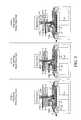
- FIG. 4is a cross sectional view showing in detail an embodiment of the ALD device 100 .
- This figuredoes not show a substrate support or susceptor and all gas valves.
- Gas A reactant gasis introduced to the manifold assembly 10 through valve 31 ( a ). Gas A is then introduced into a first compartment 82 of the dispersion portion 13 through the slits 44 in the intermediate dispersion element 43 .
- the first compartment 82is defined in part by a bottom plate having slits. Gas A reactant gas passes through the slits and flows into a second compartment 81 which is above an upper surface of the dispersion plate 3 having a plurality of bores (not shown).
- the first compartment 82 and the second compartment 81constitute a showerhead plenum.
- the first compartment 82does not have a bottom plate and there is no clear boundary between the first compartment 82 and the second compartment 81 .
- Gas Ais discharged to the reaction space 22 of the reaction chamber 1 through the bores formed in the dispersion plate 3 .
- the reaction space 22is located above the substrate support 8 ( FIG. 1 ).
- the reaction space 22is constantly exhausted using an exhaust duct 4 through an annular slit 23 , wherein the gas is drawn radially toward the outer periphery of the reaction space 22 .
- the annular slit 23is located around the outer periphery of the substrate support 8 .
- the gas dispersion portion 13is fixed to the dispersion plate 3 via an upper lid ring 113 above which an insulation plate 150 is placed.
- the gas dispersion portion 13 and the dispersion plate 3do not directly contact each other, and an annular gap 83 is formed along the outer periphery of the gas dispersion portion 13 .
- This annular gap 83communicates with the exhaust flange 19 (see FIG. 1 ) through the upper lid plate 113 .
- a purge gasis introduced thereto through one of the valves 30 ( a )-( d ), an associated one of the reactant gas valves 31 ( a )-( d ), the manifold assembly 10 , and the intermediate dispersion element 13 .
- the main purgeflows from the inert gas line 54 and through the manifold assembly 10 .
- Inert gas from the reactant gas valves 31 ( a )-( d ) and the inert gas valves 30 ( a )-( d )flush or purge the lines between the reactant valves and the central bore 28 .
- the first and second compartments 82 , 81are evacuated using the exhaust flange 19 through the annular gap 83 .
- the reaction space 22is constantly evacuated through the slit 23 and the exhaust duct 4 .
- the manifold assembly 10includes four reactant gas valves 31 ( a )-( d ), an inert channel supply line 52 , and an inert mixer supply line 54 .
- Each reactant valve 31 ( a )-( d )is paired with an inert gas valve 30 ( a )-( d ).
- Reactant valve 31 ( a )is coupled to inert valve 30 ( a ).
- Reactant valve 31 ( b )is paired with inert valve 30 ( b ).
- Reactant valve 31 ( c )is paired with inert valve 30 ( c ).
- Reactant valve 31 ( d )is paired with inert valve 30 ( d ).
- the ALD device 100can include greater or fewer reactant valves and inert valves depending on the configuration of the ALD device 100 .
- each reactant linemay or may not be paired to one inert gas valve.
- one or more of the reactant linesmay be paired to the inert gas valves while another reactant line is not.
- the reactant line that is not paired to the valvescould be purged by other means.
- Coupling 190 ( a )couples the reactant gas valve 31 ( a ) to a reactant source A 620 ( FIG. 6 ).
- Coupling 190 ( b )couples the reactant gas valve 31 ( b ) to a reactant source B 626 ( FIG. 6 ).
- Coupling 190 ( c )couples the reactant gas valve 31 ( c ) to a reactant source C 632 ( FIG. 6 ).
- Coupling 190 ( d )couples the reactant gas valve 31 ( d ) to a reactant source D 638 ( FIG. 6 ).
- Coupling 190 ( f )couples the internal inert gas channel 610 (see FIG. 6 ) to an inert or purge gas source 644 ( FIG. 6 ).
- Coupling 190 ( e )couples the central bore 28 or inside of the manifold assembly 10 with the inert gas source 644 separately from the internal inert gas channel 610 .
- inert channel supply line 52 and couplings 190 ( a )-( d )provide a flow path to a valve and toward the inside of the manifold assembly 10 .
- Inert channel supply line 52connects to the internal inert gas channel 610 .
- each of the inert gas valves 30 ( a )-( d )are located downstream of the internal inert gas channel 610 .
- Line 54provides a path to the inside of the manifold assembly 10 without passing through a valve.
- the couplings 190 ( a )-( d )flow reactant gases into the manifold assembly 10 .
- the inert gas line 54provides a passageway to flow inert gas directly to the central bore 28 .
- the resulting mixture(one reactant at a time with an inert gas) flows downward toward the reaction chamber 1 .
- An insulator plate 56lies adjacent to an insulation plate 150 ( FIG. 4 ) when assembled on the ALD device 100 .
- the manifold assembly 10includes one or more heater cartridges 180 configured to control wall temperature.
- the reactant gas passing through the manifold assembly 10is heated by the manifold and heater cartridges 180 . Controlling the temperature of the reactant gases as they pass through the manifold assembly 10 reduces the likelihood that condensation or thermal decomposition of the gas will occur.
- each reactant gas valve 31 ( a )-( d )is separately heated by one or more heater cartridges 180 .
- two of the reactant valveshave heaters to facilitate use of precursors with low vapor pressure (e.g., liquid or solid at standard conditions, such as ZrCl 2 , HfCl 2 , TMA and other metalorganics), while two do not.
- a first set of one or more heater cartridges 180may be located within the manifold assembly 10 and near to the lines carrying reactant gas A.
- a second set of one or more heater cartridges 180may be located within the manifold assembly 10 and near to the lines carrying reactant gas B.
- the first and second sets of heater cartridges 180may be separately controlled so as to heat gas A to a different temperature than gas B.
- the heater cartridges 180maintain a wall temperature up to 200° C. within the manifold assembly 10 .
- One or more thermal switchesmay be employed to monitor the temperature of the manifold assembly 10 . It will be understood that the system includes other temperature sensor and control mechanisms to maintain various components of the system at desired temperatures.
- the systemmay maintain a different temperature for a first pair of valves 30 , 31 and a second temperature for a second set of valves 30 , 31 depending on the desired processing.
- the illustrated embodimentcontemplates heater cartridges driven by temperature sensor(s) defining a single zone for temperature control of the monolithic ALD inlet manifold
- the illustrated embodimentcan also be adapted for separated zone control for each precursor within the ALD manifold. For example, in the illustrated case of 4 precursors with separate manifold paths, five zones can be provided for separate thermal control of the flow path for each precursor the center hub and each of the four precursor lines (including valves) are treated as separate zones.
- the hubcould be manufactured with a thermal air break limiting the mechanical and thermal connection between, for example, the body 27 and a base plate 606 (see FIG. 10 ) to small spot protrusions around the precursor gas inlet apertures. Additional heaters and thermocouples to monitor thermal control would be employed.
- temperatures of the flow paths upstream of the mixing pointe.g., the central bore
- FIG. 6is a schematic view of gas flow paths through the manifold assembly 10 illustrated in FIG. 5 and shows four inert gas valves 31 ( a )-( d ), each in flow communication with separate reactant gas valves 30 ( a )-( d ).
- the manifold assembly 10includes an internal inert gas channel 610 in flow communication with the four inert gas valves 30 ( a )-( d ).
- FIG. 6further illustrates the source for each reactant and inert gas.
- the reactant sourcesmay represent gas containers, bubblers or other vaporizers, depending on whether reactants are solid, liquid, or gas under standard conditions. Additional valves (not shown) associated with the reactant and inert gas sources may be located outside of the manifold assembly 10 .
- Gas Aflows from its source 620 and through line 622 before reaching reactant valve 31 ( a ).
- Reactant gas valve 31 ( a )may be configured to allow or prevent flow of gas A through line 624 and into the central bore 28 of the manifold assembly 10 depending on the desired processing step.
- Gas Bflows from its source 626 and through line 628 before reaching reactant valve 31 ( b ).
- Reactant gas valve 31 ( b )may be configured to allow or prevent flow of gas B through line 630 and into the central bore 28 of the manifold assembly 10 depending on the desired processing step.
- Gas Cflows from its source 632 and through line 634 before reaching reactant valve 31 ( c ).
- Reactant gas valve 31 ( c )may be configured to allow or prevent flow of gas C through line 636 and into the central bore 28 of the manifold assembly 10 depending on the desired processing step.
- Gas Dflows from its source 638 and through line 640 before reaching reactant valve 31 ( d ).
- Reactant gas valve 31 ( d )may be configured to allow or prevent flow of gas D through line 642 and into the central bore 28 of the manifold assembly 10 depending on the desired processing step.
- the illustrated four reactant valve embodimentis exemplary and more or less reactant valves could be used.
- the inert gasflows from source 644 (which may include multiple gas containers) and through the inert channel supply line 52 before reaching the internal inert gas channel 610 .
- the internal inert gas channel 610is preferably located within the manifold assembly 10 .
- the manifold assembly 10may be tested on a bench prior to re-assembly onto the reactor. With the inert gas channel 610 included in the manifold assembly 10 , thermal control of the inert gas is more uniform with the precursor gas since the inert gas and the precursor gas are fed through the same thermal mass or manifold assembly 10 .
- the internal inert gas channel 610is further in flow communication with one or more of the inert gas valves 30 ( a )-( d ). In the exemplary embodiment illustrated in FIG. 6 , the internal inert gas channel 610 is in flow communication with four inert gas valves 30 ( a )-( d ).
- the inert gas valve 30 ( a )is a two port valve.
- the two port valvecontrols flow of the inert gas between the internal inert gas channel 610 and the reactant gas valve 31 ( a ).
- the two port valvehas one input port in flow communication with the internal inert gas channel 610 and an output port in flow communication with reactant gas valve 31 ( a ) via line 648 .
- the inert gas valve 30 ( a )may be configured to allow or prevent flow of inert gas between line 646 and line 648 .
- Reactant gas valve 31 ( a )is in flow communication with line 648 .
- the reactant gas valve 31 ( a )is further configured to allow or prevent flow of inert gas through line 624 and into the central bore 28 of the manifold assembly 10 .
- the reactant gas valve 31 ( a )may be configured to separately allow or prevent the inert gas and the reactant gas A from entering line 624 .
- reactant gas valve 31 ( a )is a three port valve.
- a first port of reactant gas valve 31 ( a )is in flow communication with line 622 and receives reactant gas A.
- a second port of reactant gas valve 31 ( a )is in flow communication with line 648 and receives an inert gas.
- a third or exit port for reactant gas valve 31 ( a )is in flow communication with the central bore 28 of the manifold assembly 10 via line 624 .
- the inert gas valve 30 ( b )is a two port valve.
- the two port valvecontrols flow of the inert gas between the internal inert gas channel 610 and the reactant gas valve 31 ( b ).
- the two port valvehas one input port in flow communication with the internal inert gas channel 610 and an output port in flow communication with reactant gas valve 31 ( b ) via line 652 .
- the inert gas valve 30 ( b )may be configured to allow or prevent flow of inert gas between line 650 and line 652 .
- Reactant gas valve 31 ( b )is in flow communication with line 652 .
- the reactant gas valve 31 ( b )is further configured to allow or prevent flow of inert gas through line 630 and into the central bore 28 of the manifold assembly 10 .
- the reactant gas valve 31 ( b )may be configured to separately allow or prevent the inert gas and the reactant gas B from entering line 630 .
- reactant gas valve 31 ( b )is a three port valve.
- a first port of reactant gas valve 31 ( b )is in flow communication with line 628 and receives reactant gas B.
- a second port of reactant gas valve 31 ( b )is in flow communication with line 652 and receives an inert gas.
- a third or exit port for reactant gas valve 31 ( b )is in flow communication with the central bore 28 of the manifold assembly 10 via line 630 .
- the inert gas valve 30 ( c )is a two port valve.
- the two port valvecontrols flow of the inert gas between the internal inert gas channel 610 and the reactant gas valve 31 ( c ).
- the two port valvehas one input port in flow communication with the internal inert gas channel 610 and an output port in flow communication with reactant gas valve 31 ( c ) via line 656 .
- the inert gas valve 30 ( c )may be configured to allow or prevent flow of inert gas between line 654 and line 656 .
- Reactant gas valve 31 ( c )is in flow communication with line 656 .
- the reactant gas valve 31 ( c )is further configured to allow or prevent flow of inert gas through line 636 and into the central bore 28 of the manifold assembly 10 .
- the reactant gas valve 31 ( c )may be configured to separately allow or prevent the inert gas and the reactant gas C from entering line 636 .
- reactant gas valve 31 ( c )is a three port valve.
- a first port of reactant gas valve 31 ( c )is in flow communication with line 634 and receives reactant gas C.
- a second port of reactant gas valve 31 ( c )is in flow communication with line 656 and receives an inert gas.
- a third or exit port for reactant gas valve 31 ( c )is in flow communication with the central bore 28 of the manifold assembly 10 via line 636 .
- the inert gas valve 30 ( d )is a two port valve.
- the two port valvecontrols flow of the inert gas between the internal inert gas channel 610 and the reactant gas valve 31 ( d ).
- the two port valvehas one input port in flow communication with the internal inert gas channel 610 and an output port in flow communication with reactant gas valve 31 ( d ) via line 660 .
- the inert gas valve 30 ( d )may be configured to allow or prevent flow of inert gas between line 658 and line 660 .
- Reactant gas valve 31 ( d )is in flow communication with line 660 .
- the reactant gas valve 31 ( d )is further configured to allow or prevent flow of inert gas through line 642 and into the central bore 28 of the manifold assembly 10 .
- the reactant gas valve 31 ( d )may be configured to separately allow or prevent the inert gas and the reactant gas D from entering line 642 .
- reactant gas valve 31 ( d )is a three port valve.
- a first port of reactant gas valve 31 ( d )is in flow communication with line 640 and receives reactant gas D.
- a second port of reactant gas valve 31 ( d )is in flow communication with line 660 and receives an inert gas.
- a third or exit port for reactant gas valve 31 ( d )is in flow communication with the central bore 28 of the manifold assembly 10 via line 642 .
- reactant gas valve 31 ( a )is configured to allow reactant gas flow when reactant gas flowing through the valve is increased.
- reactant gas valve 31 ( a )is configured to prevent reactant gas flow when reactant gas flowing through the valve is decreased.
- the lengths of the lines illustrated in FIG. 6are for ease of identification and may shorter or longer depending on the desired configuration. In certain embodiments, it may be preferred to shorten one or more lines to reduce the amount of non-reacted reactants to be purged from the manifold assembly 10 .
- the “lines” of FIG. 6 within the manifold assembly 10are all machined channels within the central block and/or appended plates, such that the distances between the valves and the reaction chamber are minimal, reducing purge times, as will be appreciated from FIGS. 4-5 and 7 - 10 .
- An inert mixer supply line 54couples the central bore 28 or inside of the manifold assembly 10 with the inert gas source 644 separately from the internal inert gas channel 610 .
- Line 54provides a path to the central bore 28 without passing through a valve.
- a valve 662controls flow of the inert gas entering the manifold assembly 10 from line 54 .
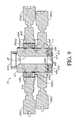
- FIG. 7is a top view of the manifold apparatus 10 from FIG. 5 illustrating reactant gas valves 31 ( a )-( d ) and inert gas valves 30 ( a )-( d ) coupled to the central body 27 of the manifold assembly 10 .
- the manifold assembly 10is configured to route reactant gases entering via couplings 190 ( a )-( d ) and inert gas entering via coupling 190 ( e ) to the central bore 28 of the manifold assembly 10 .
- the coupling 190 ( a )is in flow communication with reactant gas valve 31 ( a ) via line 622 .
- the coupling 190 ( b )is in flow communication with reactant gas valve 31 ( b ) via line 628 .
- the coupling 190 ( c )is in flow communication with reactant gas valve 31 ( c ) via line 634 .
- the coupling 190 ( d )is in flow communication with reactant gas valve 31 ( d ) via line 640 .
- the coupling 190 ( e )is in flow communication with the central bore 28 of the manifold assembly 10 via line 54 .
- the manifold assembly 10may route a single gas or multiple gases at the same time to the central bore 28 of the manifold assembly 10 during a given pulse.
- one reactant gasis mixed with inert gas in the bore 28 .
- the resulting mixtureenters the deposition chamber 1 ( FIG. 1 ).
- the ALDexhausts any unreacted reactant and inert gases from the deposition chamber via the exhaust pipe 24 and from the showerhead assembly via the showerhead exhaust valve 20 ( FIG. 1 ), such as through purging.
- Inert gasmay continually flow to the central bore 28 of the manifold assembly 10 via line 54 during processing, intermittingly, or only during purge operations. As discussed above, inert gas may also flow to the internal inert gas channel 610 via the inert channel supply line 52 ( FIG. 6 ) within the manifold assembly 10 .
- the internal inert gas channel 610is in flow communication with the inert gas valves 30 ( a )-( d ).
- each reactant gas valve 31 ( a )-( d )may be mounted on the body 27 using a spacer block 700 ( a )-( d ) which attaches to the body 27 .
- the spacer blocks 700 ( a )-( d )are provided with openings and screw holes which mate with the reactant gas valves 31 ( a )-( d ).
- the spacer blocks 700 ( a )-( d )ease manufacturing of the manifold assembly 10 .
- Spacer block 700 ( a )is associated with reactant gas valve 31 ( a ) and provides flow paths between the body 27 of the manifold assembly 10 and the reactant gas valve 31 ( a ).
- Spacer block 700 ( b )is associated with reactant gas valve 31 ( b ) and provides flow paths between the body 27 of the manifold assembly 10 and the reactant gas valve 31 ( b ).
- Spacer block 700 ( c )is associated with reactant gas valve 31 ( c ) and provides flow paths between the body 27 of the manifold assembly 10 and the reactant gas valve 31 ( c ).
- Spacer block 700 ( d )is associated with reactant gas valve 31 ( d ) and provides flow paths between the body 27 of the manifold assembly 10 and the reactant gas valve 31 ( d ).
- FIG. 8is a cross-sectional view taken along lines 8 - 8 of FIG. 7
- FIG. 9is a cross-sectional view taken along lines 9 - 9 of FIG. 7
- Each spacer block 700 ( a )-( d )provides a portion of the gas routing paths to and from the associated reactant gas valve 31 ( a )-( d ).
- the gas routing paths illustrated in FIGS. 8 and 9correspond to lines described with reference to FIG. 6 .
- An entire line described in FIG. 6may represent an entire passageway in a single component of the manifold assembly 10 or portions of passageways in multiple components of the manifold assembly 10 .
- Line 660 illustrated in FIGS. 6 and 8corresponds to at least portions of passageways in the body 27 of the manifold assembly 10 and in the spacer block 700 ( d ).
- the body 27 in the illustrated embodimenthas a tubular shape with a central bore 28 .
- the body 27includes an entrance 612 and an exit 614 .
- the central bore 28can have a lower portion having a cylindrical shape and an upper portion having a conical shape.
- the cross-sectional area in the region of the entrance 612is preferably greater than the cross-sectional area of the exit 614 .
- the cross-sectional flow area of the central bore 28gradually decreases as the mixture migrates towards the exit 614 and forms a tapered or “funnel” passage.
- the inner surface of the body 27has a conical shape which reduces the open cross-section area through the body 27 as the mixture flows towards the exit 614 .
- the body 27further includes attachment holes on the downstream or bottom surface for attaching the manifold assembly 10 to the showerhead plate of the reaction chamber 1 .
- each spacer block 700 ( a )-( d )has three distinct passageways connected to the two input ports and the single output port of the associated reactant gas valve 31 ( a )-( d ).
- a first passageway or line 652 in both the spacer block 700 ( b ) and the body 27 of the manifold assembly 10connects the output port of the inert gas valve 30 ( b ) to one of the two input ports for the reactant gas valve 31 ( b ).
- the second passageway or line 628connects coupling 190 ( b ) to the other input port for the reactant valve 31 ( b ).
- the third passageway or line 630connects the output port of the reactant gas valve 31 ( b ) with the central bore 28 of the manifold assembly 10 .
- a first passageway or line 660 in both the spacer block 700 ( d ) and the body 27 of the manifold assembly 10connects the output port of the inert gas valve 30 ( d ) to one of the two input ports for the reactant gas valve 31 ( d ).
- the second passageway or line 640connects coupling 190 ( d ) to the other input port for the reactant valve 31 ( d ).
- the third passageway or line 642connects the output port of the reactant gas valve 31 ( d ) with the central bore 28 of the manifold assembly 10 .
- the inert gas valves 30 ( a )-( d )are partially obstructed from view by the reactant gas valves 31 ( a )-( d ) in FIG. 7 .
- FIG. 9is an enlarged cross-sectional view taken along lines 9 - 9 of FIG. 7 , showing reactant valves 31 ( a ), 31 ( c ) and inert gas valves 30 ( a ), 30 ( c ) connected to the body 27 of the manifold assembly 10 .
- spacer block 700 ( a )is associated with reactant gas valve 31 ( a ) and provides flow paths between the body 27 of the manifold assembly 10 and the reactant gas valve 31 ( a ).
- Spacer block 700 ( c )is associated with reactant gas valve 31 ( c ) and provides flow paths between the body of the manifold assembly 10 and the reactant gas valve 31 ( c ).
- a first passageway or line 648 in both the spacer block 700 ( a ) and the body 27 of the manifold assembly 10connects the output port of the inert gas valve 30 ( a ) to one of the two input ports for the reactant gas valve 31 ( a ).
- the second passageway or line 622connects coupling 190 ( a ) to the other input port for the reactant valve 31 ( a ).
- the third passageway or line 624connects the output port of the reactant gas valve 31 ( a ) with the central bore 28 of the manifold assembly 10 .
- a first passageway or line 656 in both the spacer block 700 ( c ) and the body 27 of the manifold assembly 10connects the output port of the inert gas valve 30 ( c ) to one of the two input ports for the reactant gas valve 31 ( c ).
- the second passageway or line 634connects coupling 190 ( c ) to the other input port for the reactant valve 31 ( c ).
- the third passageway or line 636connects the output port of the reactant gas valve 31 ( c ) with the central bore 28 of the manifold assembly 10 .
- Passageway or line 654connects the input port of the inert gas valve 30 ( c ) with the internal inert gas channel 610 .
- Passageway or line 646connects the input port of the inert gas valve 30 ( a ) with the internal inert gas channel 610 .
- reactant gasenters the central bore 28 of the manifold assembly 10 via lines 624 , 630 , 636 , 642 preferably off center from a centerline 702 so as to swirl the gas within the central bore 28 to enhance mixing.
- Swirling gasmay promote mixing of the reactant gas with an inert gas and/or another reactant gas depending on the desired product.
- the gas mixturecircles around inside the tubular body as the mixture migrates towards the deposition chamber 1 .
- one or more of the body 27 , spacer 700 ( a )-( d ), and valve 30 ( a )-( d ), 31 ( a )-( d ) componentsare stainless steel or other metallic material. With stainless steel, the manifold assembly 10 need not include o-rings, resulting in no dead zones.
- the lines or passagewaysare integrally formed within a chemically resistant metal block or body 27 .
- the inert and reactant valves 30 , 31are stainless steel and commercially available from Swagelok Co. of Salon, Ohio.
- the Swagelok two port inert gas valves 30 ( a )-( d )are identified as part number 6LVV-MSM-ALD3T-W2-P-CS and the three port reactant gas valves 31 ( a )-( d ) are identified as part number 6LVV-MSM-ALD3T-W3-P-CS.
- Each of the metal valves 30 , 31may be sealed against the metal and preferably stainless steel spacer 700 and body 27 of the manifolds with metal seals.
- one or more components of the manifold assembly 10are made from a ceramic material.
- FIG. 9further illustrates various metal seals located between surfaces of mating components.
- more or less metal sealscould be used depending on, for example, the materials, tolerances, operating pressures, and gases associated with the mating components.
- one or more componentsmay be combined into a single component and therefore render any seals between the combined components unnecessary.
- the spacer block 700 ( a )-( d ) and associated reactant gas valve 31 ( a )-( d )could be combined into a single component and obviate the need for seals between the combined components.
- the spacer block 700 ( a )-( d ) associated with a reactant gas valvemay extend beyond the side of the reactant gas valve so as to form a spacer for the adjacent inert gas valve (see FIG. 10 ).
- the reactant gas valve and the inert gas valve associated with the reactant gas valvemay have separate spacers.
- Conventional seals 900 made from polymeric materials, such as for o-rings,are also employed to seal the manifold assembly 10 against the showerhead assembly.
- FIG. 10schematically illustrates another embodiment of a manifold assembly 10 wherein the spacer blocks comprise sub-components of dissimilar materials, such as aluminum and stainless steel, bonded between the reactant gas valve 31 ( a ) and its associated inert gas valve 30 ( a ) and the body 27 of the manifold assembly 10 .
- reactant gas valve 31 ( a ) and inert gas valve 30 ( a )are illustrated while reactant gas valves 31 ( b )-( d ) and inert gas valves 30 ( b )-( d ) are not.
- the following descriptionapplies equally to the other three pairs of reactant gas valves and associated inert gas valves 30 ( b ), 31 ( b ); 30 ( c ), 31 ( c ); 30 ( d ), 31 ( d ).
- the valves 31 ( a ), 30 ( a )are made of a stainless steel, for example 316 SS.
- Stainless steeladvantageously increases the durability of the valves over lesser strength metals.
- the body 27 of the manifold assembly 10is made from an aluminum or similar material and provides high thermal conductivity.
- aluminumis a relative light metal and provides enhanced thermal distribution in comparison to stainless steel.
- the body 27may be made from 316 stainless steel. Of course other materials may be used for the body 27 .
- FIG. 6many internal passageways within the manifold assembly 10 are shared between components.
- An interface between connecting passageways in different partsconventionally employs recesses in the mating surfaces to accommodate an o-ring or other sealing device 900 ( FIG. 9 ).
- the recesses and associated sealsincrease the likelihood of forming a dead zone at the interface. It is advantageous to have fewer recessed or embedded seals, o-rings, and any resulting dead zones along the flow paths between the central bore 28 of the manifold assembly 10 and the reactant and inert gas valves. Such dead zones would provide gaps or voids which inhibit complete purge of the flow paths.
- An incompletely purged first reactant gasmay undesirably react with a second reactant gas at the site of the void or at a location along the flow path to which the first reactant can diffuse.
- one or more membersare sandwiched between the body 27 and the valves 31 ( a ), 30 ( a ).
- an aluminum base plate 606 and a stainless steel cap 608connect the body 27 to the valves 30 ( a ), 31 ( a ).
- the base plate 606 and cap 608further connect to each other.
- the base plate 606 and cap 608are connected together before being connected to the body 27 .
- the base plate 606 and the cap 608are attached together using an explosion bonding technique known in the art. Explosion bonding fuses the dissimilar materials of the base plate 606 and cap 608 to provide a seal-free interface therebetween.
- the base plate 606is made from the same material as the body 27 to simplify their attachment to each other. In this exemplary embodiment, both are made from aluminum.
- the internal inert gas channel 610is machined in the body 27 .
- a surface of the base plate 606forms an outer surface of the internal inert gas channel 610 .
- the illustrated shape and size of the internal inert gas channel 610is only exemplary and may have a different shape and size. Further, the location of the internal inert gas channel 610 is only exemplary and may be moved from the illustrated location within the body 27 .
- the explosion bonded base plate 606 and cap 608are attached to the outer surface of the body 27 .
- An energy beam welding methodmay be employed to attach the base plate 606 to the body 27 .
- a laser beam or electron beammay be used and provide a highly focused beam of energy to weld the materials together.
- the base plate 606is electron beam welded to the body 27 .
- a metal sealis employed to form a seal between the valves 30 , 31 and the cap 608 .
- Metal sealsas opposed to polymeric o-rings, have increased chemical resistance.
- a W-shaped metal sealis employed at the interface between the valves 30 , 31 and the cap 608 .
- Metals sealsare also advantageous due to their ability to withstand higher loads without excessively deforming as compared to polymeric o-rings.
- the metal sealmay be coated or not.
- the inert gasflows from the internal inert gas channel 610 and through line 646 before reaching inert gas valve 30 ( a ).
- the bond between the body 27 and the base plate 606is an electron beam weld having no separate seals.
- the bond between the base plate 606 and the cap 608is an explosion bond having no separate seals.
- a releasable metal sealis employed between the valves 30 ( a ), 31 ( a ) and the cap 608 allowing removal of the valves 30 ( a ), 31 ( a ) for inspection, cleaning, and maintenance.
- the inert gas valve 30 ( a ) output portis in flow communication with reactant gas valve 31 ( a ) via line 648 .
- Line 648is preferably not shared among components of the internal inert gas channel 610 and requires no seals besides at the inlet and outlet for the line 648 .
- the seals sealing the exit from line 646 , the inlet to line 648 , the outlet from line 648 , the exit from line 622 , and the inlet to line 624are metal.
- the use of metal sealscan increase the seal life over conventional polymeric seals and enhance contamination exclusion due to their high chemical resistance.
- Reactant gas valve 31 ( a )is in flow communication with line 648 .
- the reactant gas valve 31 ( a )is further configured to allow or prevent flow of inert gas through line 624 and into the central bore 28 of the manifold assembly 10 .
- the reactant gas valve 31 ( a )may be configured to separately allow or prevent the inert gas and the reactant gas A from entering line 624 .
- reactant gas valve 31 ( a )is a three port valve.
- a first port of reactant gas valve 31 ( a )is in flow communication with line 622 and receives reactant gas A.
- a second port of reactant gas valve 31 ( a )is in flow communication with line 648 and receives an inert gas.
- a third or exit port for reactant gas valve 31 ( a )is in flow communication with the central bore 28 of the manifold assembly 10 via line 624 .
- Controlling the machining tolerances of the base plate 606 and cap 608can aid in aligning a first portion of a line on a first side of an interface with a second portion of that same line on a second side of the same interface thereby reducing recirculation or voids within the manifold assembly 10 .
- Controlling the surface finish and flatness on the mating surfaces of the sub-components of the manifold assembly 10can aid in sealing adjacent sub-components. In certain embodiments, a 16 to 32 micro finish surface is maintained on the sealing surfaces.
- the control systemcontrols one or more of the valves 30 , 31 to selectively allow or prevent one or more gases from reaching the central bore 28 of the manifold assembly 10 .
- the embodiments of the manifold assembly 10reduce the need for conventional seals at interfaces between components of the manifold assembly 10 . Reducing the number of conventional seals decreases the chance of forming dead legs or zones. For ALD operation, reducing dead legs reduces the duration of purging needed to avoid interaction of reactants upstream of the reaction space. Such interaction could lead to contamination or non-uniformities in the deposition on substrates. Where interfaces must occur, advanced fabrication techniques may be employed to minimize the formation of dead zones. These fabrication techniques include electron beam welding, employing metal seal technology, explosion bonding, and the like.
- the manifold assembly 10further employs discrete heaters 180 to individually control the temperature of the various gases entering the central bore 28 of the manifold assembly 10 .
Landscapes
- Chemical & Material Sciences (AREA)
- Engineering & Computer Science (AREA)
- Mechanical Engineering (AREA)
- General Chemical & Material Sciences (AREA)
- Organic Chemistry (AREA)
- Metallurgy (AREA)
- Materials Engineering (AREA)
- Chemical Kinetics & Catalysis (AREA)
- General Engineering & Computer Science (AREA)
- Physics & Mathematics (AREA)
- Electromagnetism (AREA)
- Plasma & Fusion (AREA)
- Condensed Matter Physics & Semiconductors (AREA)
- Power Engineering (AREA)
- Microelectronics & Electronic Packaging (AREA)
- Computer Hardware Design (AREA)
- Manufacturing & Machinery (AREA)
- General Physics & Mathematics (AREA)
- Chemical Vapour Deposition (AREA)
Abstract
Description
Claims (12)
Priority Applications (2)
| Application Number | Priority Date | Filing Date | Title |
|---|---|---|---|
| US11/654,372US7918938B2 (en) | 2006-01-19 | 2007-01-17 | High temperature ALD inlet manifold |
| US13/053,014US8372201B2 (en) | 2006-01-19 | 2011-03-21 | High temperature ALD inlet manifold |
Applications Claiming Priority (2)
| Application Number | Priority Date | Filing Date | Title |
|---|---|---|---|
| US76024306P | 2006-01-19 | 2006-01-19 | |
| US11/654,372US7918938B2 (en) | 2006-01-19 | 2007-01-17 | High temperature ALD inlet manifold |
Related Child Applications (1)
| Application Number | Title | Priority Date | Filing Date |
|---|---|---|---|
| US13/053,014ContinuationUS8372201B2 (en) | 2006-01-19 | 2011-03-21 | High temperature ALD inlet manifold |
Publications (2)
| Publication Number | Publication Date |
|---|---|
| US20080202416A1 US20080202416A1 (en) | 2008-08-28 |
| US7918938B2true US7918938B2 (en) | 2011-04-05 |
Family
ID=38185832
Family Applications (2)
| Application Number | Title | Priority Date | Filing Date |
|---|---|---|---|
| US11/654,372Active2029-07-09US7918938B2 (en) | 2006-01-19 | 2007-01-17 | High temperature ALD inlet manifold |
| US13/053,014ActiveUS8372201B2 (en) | 2006-01-19 | 2011-03-21 | High temperature ALD inlet manifold |
Family Applications After (1)
| Application Number | Title | Priority Date | Filing Date |
|---|---|---|---|
| US13/053,014ActiveUS8372201B2 (en) | 2006-01-19 | 2011-03-21 | High temperature ALD inlet manifold |
Country Status (6)
| Country | Link |
|---|---|
| US (2) | US7918938B2 (en) |
| JP (1) | JP5280861B2 (en) |
| KR (2) | KR101522725B1 (en) |
| CN (1) | CN101370963B (en) |
| TW (1) | TWI424084B (en) |
| WO (1) | WO2007084493A2 (en) |
Cited By (24)
| Publication number | Priority date | Publication date | Assignee | Title |
|---|---|---|---|---|
| US20100021631A1 (en)* | 2008-07-24 | 2010-01-28 | Yoshikazu Moriyama | Coating apparatus and coating method |
| US20110162580A1 (en)* | 2006-01-19 | 2011-07-07 | Asm America, Inc. | High temperature ald inlet manifold |
| US20110277690A1 (en)* | 2010-05-14 | 2011-11-17 | Sierra Solar Power, Inc. | Multi-channel gas-delivery system |
| US20120118231A1 (en)* | 2005-03-10 | 2012-05-17 | Tokyo Electron Limited | Substrate processing method, storage medium, and substrate processing apparatus |
| US20150152969A1 (en)* | 2012-02-29 | 2015-06-04 | Fujikin Incorporated | Purge line changing block joint and fluid control apparatus |
| CN104752273A (en)* | 2013-12-27 | 2015-07-01 | 株式会社日立国际电气 | Substrate processing apparatus and method for manufacturing semiconductor device |
| US9340879B2 (en) | 2014-03-18 | 2016-05-17 | Hitachi Kokusai Electric Inc. | Substrate processing apparatus, method for manufacturing semiconductor device and computer-readable recording medium |
| US9388492B2 (en) | 2011-12-27 | 2016-07-12 | Asm America, Inc. | Vapor flow control apparatus for atomic layer deposition |
| US9574268B1 (en) | 2011-10-28 | 2017-02-21 | Asm America, Inc. | Pulsed valve manifold for atomic layer deposition |
| US9748434B1 (en) | 2016-05-24 | 2017-08-29 | Tesla, Inc. | Systems, method and apparatus for curing conductive paste |
| US9954136B2 (en) | 2016-08-03 | 2018-04-24 | Tesla, Inc. | Cassette optimized for an inline annealing system |
| US9972740B2 (en) | 2015-06-07 | 2018-05-15 | Tesla, Inc. | Chemical vapor deposition tool and process for fabrication of photovoltaic structures |
| US10115856B2 (en) | 2016-10-31 | 2018-10-30 | Tesla, Inc. | System and method for curing conductive paste using induction heating |
| US10403515B2 (en)* | 2015-09-24 | 2019-09-03 | Applied Materials, Inc. | Loadlock integrated bevel etcher system |
| US10403474B2 (en)* | 2016-07-11 | 2019-09-03 | Lam Research Corporation | Collar, conical showerheads and/or top plates for reducing recirculation in a substrate processing system |
| US10662527B2 (en) | 2016-06-01 | 2020-05-26 | Asm Ip Holding B.V. | Manifolds for uniform vapor deposition |
| US10927459B2 (en) | 2017-10-16 | 2021-02-23 | Asm Ip Holding B.V. | Systems and methods for atomic layer deposition |
| US20210254216A1 (en)* | 2020-02-13 | 2021-08-19 | Asm Ip Holding B.V. | Gas distribution assembly and method of using same |
| US11492701B2 (en) | 2019-03-19 | 2022-11-08 | Asm Ip Holding B.V. | Reactor manifolds |
| US11584993B2 (en) | 2020-10-19 | 2023-02-21 | Applied Materials, Inc. | Thermally uniform deposition station |
| US11598004B2 (en)* | 2019-03-11 | 2023-03-07 | Applied Materials, Inc. | Lid assembly apparatus and methods for substrate processing chambers |
| US11830731B2 (en) | 2019-10-22 | 2023-11-28 | Asm Ip Holding B.V. | Semiconductor deposition reactor manifolds |
| US12179161B2 (en)* | 2019-10-18 | 2024-12-31 | Taiwan Semiconductor Manufacturing Company Limited | Gas mixing system for semiconductor fabrication |
| US12203168B2 (en) | 2019-08-28 | 2025-01-21 | Lam Research Corporation | Metal deposition |
Families Citing this family (430)
| Publication number | Priority date | Publication date | Assignee | Title |
|---|---|---|---|---|
| KR20090018290A (en)* | 2007-08-17 | 2009-02-20 | 에이에스엠지니텍코리아 주식회사 | Deposition equipment |
| KR101046520B1 (en)* | 2007-09-07 | 2011-07-04 | 어플라이드 머티어리얼스, 인코포레이티드 | Source gas flow path control in pecvd system to control a by-product film deposition on inside chamber |
| US7939447B2 (en)* | 2007-10-26 | 2011-05-10 | Asm America, Inc. | Inhibitors for selective deposition of silicon containing films |
| KR100949914B1 (en)* | 2007-11-28 | 2010-03-30 | 주식회사 케이씨텍 | Atomic layer deposition apparatus |
| US7655543B2 (en) | 2007-12-21 | 2010-02-02 | Asm America, Inc. | Separate injection of reactive species in selective formation of films |
| JP2009224590A (en)* | 2008-03-17 | 2009-10-01 | Tokyo Electron Ltd | Substrate treatment apparatus |
| JP2009239082A (en)* | 2008-03-27 | 2009-10-15 | Tokyo Electron Ltd | Gas feeding device, treating device, and treating method |
| FI122941B (en) | 2008-06-12 | 2012-09-14 | Beneq Oy | Device in an ALD reactor |
| US10378106B2 (en) | 2008-11-14 | 2019-08-13 | Asm Ip Holding B.V. | Method of forming insulation film by modified PEALD |
| US9394608B2 (en) | 2009-04-06 | 2016-07-19 | Asm America, Inc. | Semiconductor processing reactor and components thereof |
| US8486191B2 (en) | 2009-04-07 | 2013-07-16 | Asm America, Inc. | Substrate reactor with adjustable injectors for mixing gases within reaction chamber |
| US8802201B2 (en) | 2009-08-14 | 2014-08-12 | Asm America, Inc. | Systems and methods for thin-film deposition of metal oxides using excited nitrogen-oxygen species |
| US8580044B2 (en)* | 2010-08-13 | 2013-11-12 | Samsung Austin Semiconductor, L.P. | Apparatus for agitating and evacuating byproduct dust from a semiconductor processing chamber |
| TW201240087A (en)* | 2011-03-30 | 2012-10-01 | Anpec Electronics Corp | Power device with boundary trench structure |
| US9255346B2 (en)* | 2011-05-27 | 2016-02-09 | Crystal Solar, Incorporated | Silicon wafers by epitaxial deposition |
| US9312155B2 (en) | 2011-06-06 | 2016-04-12 | Asm Japan K.K. | High-throughput semiconductor-processing apparatus equipped with multiple dual-chamber modules |
| US10364496B2 (en) | 2011-06-27 | 2019-07-30 | Asm Ip Holding B.V. | Dual section module having shared and unshared mass flow controllers |
| US10707082B2 (en)* | 2011-07-06 | 2020-07-07 | Asm International N.V. | Methods for depositing thin films comprising indium nitride by atomic layer deposition |
| CN102868092A (en)* | 2011-07-08 | 2013-01-09 | 苏州徕卡节能电气技术有限公司 | Power saving cabinet with double front doors |
| US10854498B2 (en) | 2011-07-15 | 2020-12-01 | Asm Ip Holding B.V. | Wafer-supporting device and method for producing same |
| US20130023129A1 (en) | 2011-07-20 | 2013-01-24 | Asm America, Inc. | Pressure transmitter for a semiconductor processing environment |
| US9017481B1 (en) | 2011-10-28 | 2015-04-28 | Asm America, Inc. | Process feed management for semiconductor substrate processing |
| KR101308111B1 (en)* | 2011-11-17 | 2013-09-26 | 주식회사 유진테크 | Apparatus and method for processing substrate including exhaust ports |
| US8900364B2 (en)* | 2011-11-29 | 2014-12-02 | Intermolecular, Inc. | High productivity vapor processing system |
| JP5513544B2 (en)* | 2012-04-23 | 2014-06-04 | 東京エレクトロン株式会社 | Substrate processing equipment |
| US8985152B2 (en)* | 2012-06-15 | 2015-03-24 | Novellus Systems, Inc. | Point of use valve manifold for semiconductor fabrication equipment |
| US9558931B2 (en) | 2012-07-27 | 2017-01-31 | Asm Ip Holding B.V. | System and method for gas-phase sulfur passivation of a semiconductor surface |
| US9659799B2 (en) | 2012-08-28 | 2017-05-23 | Asm Ip Holding B.V. | Systems and methods for dynamic semiconductor process scheduling |
| US9021985B2 (en) | 2012-09-12 | 2015-05-05 | Asm Ip Holdings B.V. | Process gas management for an inductively-coupled plasma deposition reactor |
| US10714315B2 (en) | 2012-10-12 | 2020-07-14 | Asm Ip Holdings B.V. | Semiconductor reaction chamber showerhead |
| KR102003768B1 (en)* | 2012-11-13 | 2019-07-26 | 삼성디스플레이 주식회사 | Vapor deposition apparatus and method for manufacturing organic light emitting display apparatus |
| US20160376700A1 (en) | 2013-02-01 | 2016-12-29 | Asm Ip Holding B.V. | System for treatment of deposition reactor |
| US9589770B2 (en) | 2013-03-08 | 2017-03-07 | Asm Ip Holding B.V. | Method and systems for in-situ formation of intermediate reactive species |
| US9484191B2 (en) | 2013-03-08 | 2016-11-01 | Asm Ip Holding B.V. | Pulsed remote plasma method and system |
| US8993054B2 (en) | 2013-07-12 | 2015-03-31 | Asm Ip Holding B.V. | Method and system to reduce outgassing in a reaction chamber |
| US9240412B2 (en) | 2013-09-27 | 2016-01-19 | Asm Ip Holding B.V. | Semiconductor structure and device and methods of forming same using selective epitaxial process |
| KR102173047B1 (en)* | 2013-10-10 | 2020-11-03 | 삼성디스플레이 주식회사 | Vapor deposition apparatus |
| US9605343B2 (en) | 2013-11-13 | 2017-03-28 | Asm Ip Holding B.V. | Method for forming conformal carbon films, structures conformal carbon film, and system of forming same |
| JP5971870B2 (en)* | 2013-11-29 | 2016-08-17 | 株式会社日立国際電気 | Substrate processing apparatus, semiconductor device manufacturing method, and recording medium |
| JP5859583B2 (en)* | 2014-01-30 | 2016-02-10 | 株式会社日立国際電気 | Substrate processing apparatus and semiconductor device manufacturing method |
| US10683571B2 (en)* | 2014-02-25 | 2020-06-16 | Asm Ip Holding B.V. | Gas supply manifold and method of supplying gases to chamber using same |
| US9284644B2 (en)* | 2014-02-27 | 2016-03-15 | Lam Research Corporation | Apparatus and method for improving wafer uniformity |
| US10167557B2 (en) | 2014-03-18 | 2019-01-01 | Asm Ip Holding B.V. | Gas distribution system, reactor including the system, and methods of using the same |
| US11015245B2 (en) | 2014-03-19 | 2021-05-25 | Asm Ip Holding B.V. | Gas-phase reactor and system having exhaust plenum and components thereof |
| JP5762602B1 (en)* | 2014-06-24 | 2015-08-12 | 株式会社日立国際電気 | Substrate processing apparatus, semiconductor device manufacturing method, and program |
| JP6001015B2 (en) | 2014-07-04 | 2016-10-05 | 株式会社日立国際電気 | Substrate processing apparatus, semiconductor device manufacturing method, program, and recording medium |
| JP6446881B2 (en)* | 2014-07-17 | 2019-01-09 | 東京エレクトロン株式会社 | Gas supply device and valve device |
| US10858737B2 (en) | 2014-07-28 | 2020-12-08 | Asm Ip Holding B.V. | Showerhead assembly and components thereof |
| US9890456B2 (en)* | 2014-08-21 | 2018-02-13 | Asm Ip Holding B.V. | Method and system for in situ formation of gas-phase compounds |
| JP5800969B1 (en) | 2014-08-27 | 2015-10-28 | 株式会社日立国際電気 | Substrate processing apparatus, semiconductor device manufacturing method, program, and recording medium |
| WO2016043033A1 (en) | 2014-09-17 | 2016-03-24 | 東京エレクトロン株式会社 | Shower head and deposition system |
| US10941490B2 (en) | 2014-10-07 | 2021-03-09 | Asm Ip Holding B.V. | Multiple temperature range susceptor, assembly, reactor and system including the susceptor, and methods of using the same |
| US9657845B2 (en) | 2014-10-07 | 2017-05-23 | Asm Ip Holding B.V. | Variable conductance gas distribution apparatus and method |
| KR102300403B1 (en) | 2014-11-19 | 2021-09-09 | 에이에스엠 아이피 홀딩 비.브이. | Method of depositing thin film |
| KR102263121B1 (en) | 2014-12-22 | 2021-06-09 | 에이에스엠 아이피 홀딩 비.브이. | Semiconductor device and manufacuring method thereof |
| US9963782B2 (en)* | 2015-02-12 | 2018-05-08 | Asm Ip Holding B.V. | Semiconductor manufacturing apparatus |
| US10529542B2 (en) | 2015-03-11 | 2020-01-07 | Asm Ip Holdings B.V. | Cross-flow reactor and method |
| US10276355B2 (en) | 2015-03-12 | 2019-04-30 | Asm Ip Holding B.V. | Multi-zone reactor, system including the reactor, and method of using the same |
| US11384432B2 (en)* | 2015-04-22 | 2022-07-12 | Applied Materials, Inc. | Atomic layer deposition chamber with funnel-shaped gas dispersion channel and gas distribution plate |
| KR20160147482A (en)* | 2015-06-15 | 2016-12-23 | 삼성전자주식회사 | Apparatus for manufacturing Semiconductor Devices Having a Gas Mixing Part |
| US10458018B2 (en) | 2015-06-26 | 2019-10-29 | Asm Ip Holding B.V. | Structures including metal carbide material, devices including the structures, and methods of forming same |
| US10600673B2 (en) | 2015-07-07 | 2020-03-24 | Asm Ip Holding B.V. | Magnetic susceptor to baseplate seal |
| US10043661B2 (en) | 2015-07-13 | 2018-08-07 | Asm Ip Holding B.V. | Method for protecting layer by forming hydrocarbon-based extremely thin film |
| US10083836B2 (en) | 2015-07-24 | 2018-09-25 | Asm Ip Holding B.V. | Formation of boron-doped titanium metal films with high work function |
| US10087525B2 (en) | 2015-08-04 | 2018-10-02 | Asm Ip Holding B.V. | Variable gap hard stop design |
| US9647114B2 (en) | 2015-08-14 | 2017-05-09 | Asm Ip Holding B.V. | Methods of forming highly p-type doped germanium tin films and structures and devices including the films |
| US9960072B2 (en) | 2015-09-29 | 2018-05-01 | Asm Ip Holding B.V. | Variable adjustment for precise matching of multiple chamber cavity housings |
| US10211308B2 (en) | 2015-10-21 | 2019-02-19 | Asm Ip Holding B.V. | NbMC layers |
| US10322384B2 (en) | 2015-11-09 | 2019-06-18 | Asm Ip Holding B.V. | Counter flow mixer for process chamber |
| JP6333232B2 (en)* | 2015-12-02 | 2018-05-30 | 株式会社日立国際電気 | Substrate processing apparatus, semiconductor device manufacturing method, and program |
| US20170162366A1 (en)* | 2015-12-08 | 2017-06-08 | Asm Ip Holding B.V. | Film forming apparatus, recording medium, and film forming method |
| US9627221B1 (en) | 2015-12-28 | 2017-04-18 | Asm Ip Holding B.V. | Continuous process incorporating atomic layer etching |
| US11139308B2 (en) | 2015-12-29 | 2021-10-05 | Asm Ip Holding B.V. | Atomic layer deposition of III-V compounds to form V-NAND devices |
| US10215317B2 (en)* | 2016-01-15 | 2019-02-26 | Lam Research Corporation | Additively manufactured gas distribution manifold |
| US10529554B2 (en) | 2016-02-19 | 2020-01-07 | Asm Ip Holding B.V. | Method for forming silicon nitride film selectively on sidewalls or flat surfaces of trenches |
| US10468251B2 (en) | 2016-02-19 | 2019-11-05 | Asm Ip Holding B.V. | Method for forming spacers using silicon nitride film for spacer-defined multiple patterning |
| US10501866B2 (en) | 2016-03-09 | 2019-12-10 | Asm Ip Holding B.V. | Gas distribution apparatus for improved film uniformity in an epitaxial system |
| KR102632725B1 (en) | 2016-03-17 | 2024-02-05 | 에이에스엠 아이피 홀딩 비.브이. | Substrate support plate, thin film deposition apparatus including the same, and thin film deposition method |
| US10343920B2 (en) | 2016-03-18 | 2019-07-09 | Asm Ip Holding B.V. | Aligned carbon nanotubes |
| US9892913B2 (en) | 2016-03-24 | 2018-02-13 | Asm Ip Holding B.V. | Radial and thickness control via biased multi-port injection settings |
| US10190213B2 (en) | 2016-04-21 | 2019-01-29 | Asm Ip Holding B.V. | Deposition of metal borides |
| US10865475B2 (en) | 2016-04-21 | 2020-12-15 | Asm Ip Holding B.V. | Deposition of metal borides and silicides |
| US10087522B2 (en) | 2016-04-21 | 2018-10-02 | Asm Ip Holding B.V. | Deposition of metal borides |
| US10367080B2 (en) | 2016-05-02 | 2019-07-30 | Asm Ip Holding B.V. | Method of forming a germanium oxynitride film |
| US10032628B2 (en) | 2016-05-02 | 2018-07-24 | Asm Ip Holding B.V. | Source/drain performance through conformal solid state doping |
| KR102592471B1 (en) | 2016-05-17 | 2023-10-20 | 에이에스엠 아이피 홀딩 비.브이. | Method of forming metal interconnection and method of fabricating semiconductor device using the same |
| US11453943B2 (en) | 2016-05-25 | 2022-09-27 | Asm Ip Holding B.V. | Method for forming carbon-containing silicon/metal oxide or nitride film by ALD using silicon precursor and hydrocarbon precursor |
| CN105839079B (en)* | 2016-06-07 | 2019-05-14 | 江苏微导纳米装备科技有限公司 | Vacuum coater |
| US10388509B2 (en) | 2016-06-28 | 2019-08-20 | Asm Ip Holding B.V. | Formation of epitaxial layers via dislocation filtering |
| US10612137B2 (en) | 2016-07-08 | 2020-04-07 | Asm Ip Holdings B.V. | Organic reactants for atomic layer deposition |
| US9859151B1 (en) | 2016-07-08 | 2018-01-02 | Asm Ip Holding B.V. | Selective film deposition method to form air gaps |
| US9793135B1 (en) | 2016-07-14 | 2017-10-17 | ASM IP Holding B.V | Method of cyclic dry etching using etchant film |
| KR102514043B1 (en) | 2016-07-18 | 2023-03-24 | 삼성전자주식회사 | Method of manufacturing semiconductor device |
| US10714385B2 (en) | 2016-07-19 | 2020-07-14 | Asm Ip Holding B.V. | Selective deposition of tungsten |
| KR102354490B1 (en) | 2016-07-27 | 2022-01-21 | 에이에스엠 아이피 홀딩 비.브이. | Method of processing a substrate |
| US10177025B2 (en) | 2016-07-28 | 2019-01-08 | Asm Ip Holding B.V. | Method and apparatus for filling a gap |
| US9812320B1 (en) | 2016-07-28 | 2017-11-07 | Asm Ip Holding B.V. | Method and apparatus for filling a gap |
| US10395919B2 (en) | 2016-07-28 | 2019-08-27 | Asm Ip Holding B.V. | Method and apparatus for filling a gap |
| KR102532607B1 (en) | 2016-07-28 | 2023-05-15 | 에이에스엠 아이피 홀딩 비.브이. | Substrate processing apparatus and method of operating the same |
| US9887082B1 (en) | 2016-07-28 | 2018-02-06 | Asm Ip Holding B.V. | Method and apparatus for filling a gap |
| US10090316B2 (en) | 2016-09-01 | 2018-10-02 | Asm Ip Holding B.V. | 3D stacked multilayer semiconductor memory using doped select transistor channel |
| US10410943B2 (en) | 2016-10-13 | 2019-09-10 | Asm Ip Holding B.V. | Method for passivating a surface of a semiconductor and related systems |
| US10643826B2 (en) | 2016-10-26 | 2020-05-05 | Asm Ip Holdings B.V. | Methods for thermally calibrating reaction chambers |
| US11532757B2 (en) | 2016-10-27 | 2022-12-20 | Asm Ip Holding B.V. | Deposition of charge trapping layers |
| US10435790B2 (en) | 2016-11-01 | 2019-10-08 | Asm Ip Holding B.V. | Method of subatmospheric plasma-enhanced ALD using capacitively coupled electrodes with narrow gap |
| US10229833B2 (en) | 2016-11-01 | 2019-03-12 | Asm Ip Holding B.V. | Methods for forming a transition metal nitride film on a substrate by atomic layer deposition and related semiconductor device structures |
| US10714350B2 (en) | 2016-11-01 | 2020-07-14 | ASM IP Holdings, B.V. | Methods for forming a transition metal niobium nitride film on a substrate by atomic layer deposition and related semiconductor device structures |
| US10643904B2 (en) | 2016-11-01 | 2020-05-05 | Asm Ip Holdings B.V. | Methods for forming a semiconductor device and related semiconductor device structures |
| US10134757B2 (en) | 2016-11-07 | 2018-11-20 | Asm Ip Holding B.V. | Method of processing a substrate and a device manufactured by using the method |
| KR102546317B1 (en) | 2016-11-15 | 2023-06-21 | 에이에스엠 아이피 홀딩 비.브이. | Gas supply unit and substrate processing apparatus including the same |
| US10340135B2 (en) | 2016-11-28 | 2019-07-02 | Asm Ip Holding B.V. | Method of topologically restricted plasma-enhanced cyclic deposition of silicon or metal nitride |
| KR102204297B1 (en)* | 2016-12-02 | 2021-01-15 | 어플라이드 머티어리얼스, 인코포레이티드 | Thin Film Encapsulation Processing System and Process Kit |
| KR102762543B1 (en)* | 2016-12-14 | 2025-02-05 | 에이에스엠 아이피 홀딩 비.브이. | Substrate processing apparatus |
| US11581186B2 (en) | 2016-12-15 | 2023-02-14 | Asm Ip Holding B.V. | Sequential infiltration synthesis apparatus |
| US9916980B1 (en) | 2016-12-15 | 2018-03-13 | Asm Ip Holding B.V. | Method of forming a structure on a substrate |
| US11447861B2 (en) | 2016-12-15 | 2022-09-20 | Asm Ip Holding B.V. | Sequential infiltration synthesis apparatus and a method of forming a patterned structure |
| KR102700194B1 (en)* | 2016-12-19 | 2024-08-28 | 에이에스엠 아이피 홀딩 비.브이. | Substrate processing apparatus |
| US10269558B2 (en) | 2016-12-22 | 2019-04-23 | Asm Ip Holding B.V. | Method of forming a structure on a substrate |
| US10867788B2 (en) | 2016-12-28 | 2020-12-15 | Asm Ip Holding B.V. | Method of forming a structure on a substrate |
| US11390950B2 (en) | 2017-01-10 | 2022-07-19 | Asm Ip Holding B.V. | Reactor system and method to reduce residue buildup during a film deposition process |
| WO2018146370A1 (en) | 2017-02-08 | 2018-08-16 | Picosun Oy | Deposition or cleaning apparatus with movable structure and method of operation |
| US10655221B2 (en) | 2017-02-09 | 2020-05-19 | Asm Ip Holding B.V. | Method for depositing oxide film by thermal ALD and PEALD |
| US10468261B2 (en) | 2017-02-15 | 2019-11-05 | Asm Ip Holding B.V. | Methods for forming a metallic film on a substrate by cyclical deposition and related semiconductor device structures |
| US10400332B2 (en)* | 2017-03-14 | 2019-09-03 | Eastman Kodak Company | Deposition system with interlocking deposition heads |
| US10529563B2 (en) | 2017-03-29 | 2020-01-07 | Asm Ip Holdings B.V. | Method for forming doped metal oxide films on a substrate by cyclical deposition and related semiconductor device structures |
| US10283353B2 (en) | 2017-03-29 | 2019-05-07 | Asm Ip Holding B.V. | Method of reforming insulating film deposited on substrate with recess pattern |
| US10103040B1 (en) | 2017-03-31 | 2018-10-16 | Asm Ip Holding B.V. | Apparatus and method for manufacturing a semiconductor device |
| USD830981S1 (en) | 2017-04-07 | 2018-10-16 | Asm Ip Holding B.V. | Susceptor for semiconductor substrate processing apparatus |
| KR102457289B1 (en) | 2017-04-25 | 2022-10-21 | 에이에스엠 아이피 홀딩 비.브이. | Method for depositing a thin film and manufacturing a semiconductor device |
| US10446393B2 (en) | 2017-05-08 | 2019-10-15 | Asm Ip Holding B.V. | Methods for forming silicon-containing epitaxial layers and related semiconductor device structures |
| US10770286B2 (en) | 2017-05-08 | 2020-09-08 | Asm Ip Holdings B.V. | Methods for selectively forming a silicon nitride film on a substrate and related semiconductor device structures |
| US10892156B2 (en) | 2017-05-08 | 2021-01-12 | Asm Ip Holding B.V. | Methods for forming a silicon nitride film on a substrate and related semiconductor device structures |
| CN116978782A (en)* | 2017-05-12 | 2023-10-31 | 应用材料公司 | Deposition of metal silicide layers on substrates and chamber components |
| US10504742B2 (en) | 2017-05-31 | 2019-12-10 | Asm Ip Holding B.V. | Method of atomic layer etching using hydrogen plasma |
| US10886123B2 (en) | 2017-06-02 | 2021-01-05 | Asm Ip Holding B.V. | Methods for forming low temperature semiconductor layers and related semiconductor device structures |
| US12040200B2 (en) | 2017-06-20 | 2024-07-16 | Asm Ip Holding B.V. | Semiconductor processing apparatus and methods for calibrating a semiconductor processing apparatus |
| US11306395B2 (en) | 2017-06-28 | 2022-04-19 | Asm Ip Holding B.V. | Methods for depositing a transition metal nitride film on a substrate by atomic layer deposition and related deposition apparatus |
| US10685834B2 (en) | 2017-07-05 | 2020-06-16 | Asm Ip Holdings B.V. | Methods for forming a silicon germanium tin layer and related semiconductor device structures |
| KR20190009245A (en) | 2017-07-18 | 2019-01-28 | 에이에스엠 아이피 홀딩 비.브이. | Methods for forming a semiconductor device structure and related semiconductor device structures |
| US11374112B2 (en) | 2017-07-19 | 2022-06-28 | Asm Ip Holding B.V. | Method for depositing a group IV semiconductor and related semiconductor device structures |
| US10541333B2 (en) | 2017-07-19 | 2020-01-21 | Asm Ip Holding B.V. | Method for depositing a group IV semiconductor and related semiconductor device structures |
| US11018002B2 (en) | 2017-07-19 | 2021-05-25 | Asm Ip Holding B.V. | Method for selectively depositing a Group IV semiconductor and related semiconductor device structures |
| US10312055B2 (en) | 2017-07-26 | 2019-06-04 | Asm Ip Holding B.V. | Method of depositing film by PEALD using negative bias |
| US10590535B2 (en) | 2017-07-26 | 2020-03-17 | Asm Ip Holdings B.V. | Chemical treatment, deposition and/or infiltration apparatus and method for using the same |
| US10605530B2 (en) | 2017-07-26 | 2020-03-31 | Asm Ip Holding B.V. | Assembly of a liner and a flange for a vertical furnace as well as the liner and the vertical furnace |
| CN109321897B (en)* | 2017-07-31 | 2022-01-07 | 北京北方华创微电子装备有限公司 | Atomic layer deposition system and method |
| TWI815813B (en) | 2017-08-04 | 2023-09-21 | 荷蘭商Asm智慧財產控股公司 | Showerhead assembly for distributing a gas within a reaction chamber |
| US10770336B2 (en) | 2017-08-08 | 2020-09-08 | Asm Ip Holding B.V. | Substrate lift mechanism and reactor including same |
| US10692741B2 (en) | 2017-08-08 | 2020-06-23 | Asm Ip Holdings B.V. | Radiation shield |
| US10249524B2 (en) | 2017-08-09 | 2019-04-02 | Asm Ip Holding B.V. | Cassette holder assembly for a substrate cassette and holding member for use in such assembly |
| US11769682B2 (en) | 2017-08-09 | 2023-09-26 | Asm Ip Holding B.V. | Storage apparatus for storing cassettes for substrates and processing apparatus equipped therewith |
| US11139191B2 (en) | 2017-08-09 | 2021-10-05 | Asm Ip Holding B.V. | Storage apparatus for storing cassettes for substrates and processing apparatus equipped therewith |
| US20190048467A1 (en)* | 2017-08-10 | 2019-02-14 | Applied Materials, Inc. | Showerhead and process chamber incorporating same |
| US10236177B1 (en) | 2017-08-22 | 2019-03-19 | ASM IP Holding B.V.. | Methods for depositing a doped germanium tin semiconductor and related semiconductor device structures |
| USD900036S1 (en) | 2017-08-24 | 2020-10-27 | Asm Ip Holding B.V. | Heater electrical connector and adapter |
| JP2020532658A (en) | 2017-08-24 | 2020-11-12 | フォージ ナノ,インコーポレイティド | Manufacturing methods and uses for synthesizing, functionalizing, surface treating and / or encapsulating powders |
| US11830730B2 (en) | 2017-08-29 | 2023-11-28 | Asm Ip Holding B.V. | Layer forming method and apparatus |
| US11056344B2 (en) | 2017-08-30 | 2021-07-06 | Asm Ip Holding B.V. | Layer forming method |
| US11295980B2 (en) | 2017-08-30 | 2022-04-05 | Asm Ip Holding B.V. | Methods for depositing a molybdenum metal film over a dielectric surface of a substrate by a cyclical deposition process and related semiconductor device structures |
| KR102491945B1 (en) | 2017-08-30 | 2023-01-26 | 에이에스엠 아이피 홀딩 비.브이. | Substrate processing apparatus |
| KR102401446B1 (en) | 2017-08-31 | 2022-05-24 | 에이에스엠 아이피 홀딩 비.브이. | Substrate processing apparatus |
| US10607895B2 (en) | 2017-09-18 | 2020-03-31 | Asm Ip Holdings B.V. | Method for forming a semiconductor device structure comprising a gate fill metal |
| KR102630301B1 (en) | 2017-09-21 | 2024-01-29 | 에이에스엠 아이피 홀딩 비.브이. | Method of sequential infiltration synthesis treatment of infiltrateable material and structures and devices formed using same |
| US10844484B2 (en) | 2017-09-22 | 2020-11-24 | Asm Ip Holding B.V. | Apparatus for dispensing a vapor phase reactant to a reaction chamber and related methods |
| US10658205B2 (en) | 2017-09-28 | 2020-05-19 | Asm Ip Holdings B.V. | Chemical dispensing apparatus and methods for dispensing a chemical to a reaction chamber |
| US10403504B2 (en) | 2017-10-05 | 2019-09-03 | Asm Ip Holding B.V. | Method for selectively depositing a metallic film on a substrate |
| US10319588B2 (en) | 2017-10-10 | 2019-06-11 | Asm Ip Holding B.V. | Method for depositing a metal chalcogenide on a substrate by cyclical deposition |
| US10923344B2 (en) | 2017-10-30 | 2021-02-16 | Asm Ip Holding B.V. | Methods for forming a semiconductor structure and related semiconductor structures |
| KR102443047B1 (en) | 2017-11-16 | 2022-09-14 | 에이에스엠 아이피 홀딩 비.브이. | Method of processing a substrate and a device manufactured by the same |
| US10910262B2 (en) | 2017-11-16 | 2021-02-02 | Asm Ip Holding B.V. | Method of selectively depositing a capping layer structure on a semiconductor device structure |
| US11022879B2 (en) | 2017-11-24 | 2021-06-01 | Asm Ip Holding B.V. | Method of forming an enhanced unexposed photoresist layer |
| CN111344522B (en) | 2017-11-27 | 2022-04-12 | 阿斯莫Ip控股公司 | Including clean mini-environment device |
| WO2019103613A1 (en) | 2017-11-27 | 2019-05-31 | Asm Ip Holding B.V. | A storage device for storing wafer cassettes for use with a batch furnace |
| US10290508B1 (en) | 2017-12-05 | 2019-05-14 | Asm Ip Holding B.V. | Method for forming vertical spacers for spacer-defined patterning |
| US10872771B2 (en) | 2018-01-16 | 2020-12-22 | Asm Ip Holding B. V. | Method for depositing a material film on a substrate within a reaction chamber by a cyclical deposition process and related device structures |
| KR102695659B1 (en) | 2018-01-19 | 2024-08-14 | 에이에스엠 아이피 홀딩 비.브이. | Method for depositing a gap filling layer by plasma assisted deposition |
| TWI799494B (en) | 2018-01-19 | 2023-04-21 | 荷蘭商Asm 智慧財產控股公司 | Deposition method |
| USD903477S1 (en) | 2018-01-24 | 2020-12-01 | Asm Ip Holdings B.V. | Metal clamp |
| US11018047B2 (en) | 2018-01-25 | 2021-05-25 | Asm Ip Holding B.V. | Hybrid lift pin |
| US10535516B2 (en) | 2018-02-01 | 2020-01-14 | Asm Ip Holdings B.V. | Method for depositing a semiconductor structure on a surface of a substrate and related semiconductor structures |
| USD880437S1 (en) | 2018-02-01 | 2020-04-07 | Asm Ip Holding B.V. | Gas supply plate for semiconductor manufacturing apparatus |
| US11081345B2 (en) | 2018-02-06 | 2021-08-03 | Asm Ip Holding B.V. | Method of post-deposition treatment for silicon oxide film |
| WO2019158960A1 (en) | 2018-02-14 | 2019-08-22 | Asm Ip Holding B.V. | A method for depositing a ruthenium-containing film on a substrate by a cyclical deposition process |
| US10896820B2 (en) | 2018-02-14 | 2021-01-19 | Asm Ip Holding B.V. | Method for depositing a ruthenium-containing film on a substrate by a cyclical deposition process |
| US10731249B2 (en) | 2018-02-15 | 2020-08-04 | Asm Ip Holding B.V. | Method of forming a transition metal containing film on a substrate by a cyclical deposition process, a method for supplying a transition metal halide compound to a reaction chamber, and related vapor deposition apparatus |
| US10658181B2 (en) | 2018-02-20 | 2020-05-19 | Asm Ip Holding B.V. | Method of spacer-defined direct patterning in semiconductor fabrication |
| KR102636427B1 (en) | 2018-02-20 | 2024-02-13 | 에이에스엠 아이피 홀딩 비.브이. | Substrate processing method and apparatus |
| US10975470B2 (en) | 2018-02-23 | 2021-04-13 | Asm Ip Holding B.V. | Apparatus for detecting or monitoring for a chemical precursor in a high temperature environment |
| US11473195B2 (en) | 2018-03-01 | 2022-10-18 | Asm Ip Holding B.V. | Semiconductor processing apparatus and a method for processing a substrate |
| US11629406B2 (en) | 2018-03-09 | 2023-04-18 | Asm Ip Holding B.V. | Semiconductor processing apparatus comprising one or more pyrometers for measuring a temperature of a substrate during transfer of the substrate |
| US11114283B2 (en) | 2018-03-16 | 2021-09-07 | Asm Ip Holding B.V. | Reactor, system including the reactor, and methods of manufacturing and using same |
| KR102646467B1 (en) | 2018-03-27 | 2024-03-11 | 에이에스엠 아이피 홀딩 비.브이. | Method of forming an electrode on a substrate and a semiconductor device structure including an electrode |
| US11088002B2 (en) | 2018-03-29 | 2021-08-10 | Asm Ip Holding B.V. | Substrate rack and a substrate processing system and method |
| US10510536B2 (en) | 2018-03-29 | 2019-12-17 | Asm Ip Holding B.V. | Method of depositing a co-doped polysilicon film on a surface of a substrate within a reaction chamber |
| US11230766B2 (en) | 2018-03-29 | 2022-01-25 | Asm Ip Holding B.V. | Substrate processing apparatus and method |
| KR102501472B1 (en) | 2018-03-30 | 2023-02-20 | 에이에스엠 아이피 홀딩 비.브이. | Substrate processing method |
| KR102600229B1 (en) | 2018-04-09 | 2023-11-10 | 에이에스엠 아이피 홀딩 비.브이. | Substrate supporting device, substrate processing apparatus including the same and substrate processing method |
| TWI811348B (en) | 2018-05-08 | 2023-08-11 | 荷蘭商Asm 智慧財產控股公司 | Methods for depositing an oxide film on a substrate by a cyclical deposition process and related device structures |
| US12025484B2 (en) | 2018-05-08 | 2024-07-02 | Asm Ip Holding B.V. | Thin film forming method |
| US12272527B2 (en) | 2018-05-09 | 2025-04-08 | Asm Ip Holding B.V. | Apparatus for use with hydrogen radicals and method of using same |
| KR20190129718A (en) | 2018-05-11 | 2019-11-20 | 에이에스엠 아이피 홀딩 비.브이. | Methods for forming a doped metal carbide film on a substrate and related semiconductor device structures |
| KR102596988B1 (en) | 2018-05-28 | 2023-10-31 | 에이에스엠 아이피 홀딩 비.브이. | Method of processing a substrate and a device manufactured by the same |
| TWI840362B (en) | 2018-06-04 | 2024-05-01 | 荷蘭商Asm Ip私人控股有限公司 | Wafer handling chamber with moisture reduction |
| US11718913B2 (en) | 2018-06-04 | 2023-08-08 | Asm Ip Holding B.V. | Gas distribution system and reactor system including same |
| US11286562B2 (en) | 2018-06-08 | 2022-03-29 | Asm Ip Holding B.V. | Gas-phase chemical reactor and method of using same |
| US10797133B2 (en) | 2018-06-21 | 2020-10-06 | Asm Ip Holding B.V. | Method for depositing a phosphorus doped silicon arsenide film and related semiconductor device structures |
| KR102568797B1 (en) | 2018-06-21 | 2023-08-21 | 에이에스엠 아이피 홀딩 비.브이. | Substrate processing system |
| TWI873894B (en) | 2018-06-27 | 2025-02-21 | 荷蘭商Asm Ip私人控股有限公司 | Cyclic deposition methods for forming metal-containing material and films and structures including the metal-containing material |
| KR102854019B1 (en) | 2018-06-27 | 2025-09-02 | 에이에스엠 아이피 홀딩 비.브이. | Periodic deposition method for forming a metal-containing material and films and structures comprising the metal-containing material |
| KR102686758B1 (en) | 2018-06-29 | 2024-07-18 | 에이에스엠 아이피 홀딩 비.브이. | Method for depositing a thin film and manufacturing a semiconductor device |
| US10612136B2 (en) | 2018-06-29 | 2020-04-07 | ASM IP Holding, B.V. | Temperature-controlled flange and reactor system including same |
| US10388513B1 (en) | 2018-07-03 | 2019-08-20 | Asm Ip Holding B.V. | Method for depositing silicon-free carbon-containing film as gap-fill layer by pulse plasma-assisted deposition |
| US10755922B2 (en) | 2018-07-03 | 2020-08-25 | Asm Ip Holding B.V. | Method for depositing silicon-free carbon-containing film as gap-fill layer by pulse plasma-assisted deposition |
| US10767789B2 (en) | 2018-07-16 | 2020-09-08 | Asm Ip Holding B.V. | Diaphragm valves, valve components, and methods for forming valve components |
| US10483099B1 (en) | 2018-07-26 | 2019-11-19 | Asm Ip Holding B.V. | Method for forming thermally stable organosilicon polymer film |
| US11053591B2 (en) | 2018-08-06 | 2021-07-06 | Asm Ip Holding B.V. | Multi-port gas injection system and reactor system including same |
| US10883175B2 (en) | 2018-08-09 | 2021-01-05 | Asm Ip Holding B.V. | Vertical furnace for processing substrates and a liner for use therein |
| US10829852B2 (en) | 2018-08-16 | 2020-11-10 | Asm Ip Holding B.V. | Gas distribution device for a wafer processing apparatus |
| US11430674B2 (en) | 2018-08-22 | 2022-08-30 | Asm Ip Holding B.V. | Sensor array, apparatus for dispensing a vapor phase reactant to a reaction chamber and related methods |
| JP7119779B2 (en)* | 2018-08-30 | 2022-08-17 | 住友金属鉱山株式会社 | Deposition apparatus and deposition method |
| US11024523B2 (en) | 2018-09-11 | 2021-06-01 | Asm Ip Holding B.V. | Substrate processing apparatus and method |
| KR102707956B1 (en) | 2018-09-11 | 2024-09-19 | 에이에스엠 아이피 홀딩 비.브이. | Method for deposition of a thin film |
| US11049751B2 (en) | 2018-09-14 | 2021-06-29 | Asm Ip Holding B.V. | Cassette supply system to store and handle cassettes and processing apparatus equipped therewith |
| CN110970344B (en) | 2018-10-01 | 2024-10-25 | Asmip控股有限公司 | Substrate holding apparatus, system comprising the same and method of using the same |
| US11232963B2 (en) | 2018-10-03 | 2022-01-25 | Asm Ip Holding B.V. | Substrate processing apparatus and method |
| KR102592699B1 (en) | 2018-10-08 | 2023-10-23 | 에이에스엠 아이피 홀딩 비.브이. | Substrate support unit and apparatuses for depositing thin film and processing the substrate including the same |
| US10847365B2 (en) | 2018-10-11 | 2020-11-24 | Asm Ip Holding B.V. | Method of forming conformal silicon carbide film by cyclic CVD |
| US10811256B2 (en) | 2018-10-16 | 2020-10-20 | Asm Ip Holding B.V. | Method for etching a carbon-containing feature |
| KR102546322B1 (en) | 2018-10-19 | 2023-06-21 | 에이에스엠 아이피 홀딩 비.브이. | Substrate processing apparatus and substrate processing method |
| KR102605121B1 (en) | 2018-10-19 | 2023-11-23 | 에이에스엠 아이피 홀딩 비.브이. | Substrate processing apparatus and substrate processing method |
| USD948463S1 (en) | 2018-10-24 | 2022-04-12 | Asm Ip Holding B.V. | Susceptor for semiconductor substrate supporting apparatus |
| US10381219B1 (en) | 2018-10-25 | 2019-08-13 | Asm Ip Holding B.V. | Methods for forming a silicon nitride film |
| US12378665B2 (en) | 2018-10-26 | 2025-08-05 | Asm Ip Holding B.V. | High temperature coatings for a preclean and etch apparatus and related methods |
| US11087997B2 (en) | 2018-10-31 | 2021-08-10 | Asm Ip Holding B.V. | Substrate processing apparatus for processing substrates |
| KR102748291B1 (en) | 2018-11-02 | 2024-12-31 | 에이에스엠 아이피 홀딩 비.브이. | Substrate support unit and substrate processing apparatus including the same |
| US11572620B2 (en) | 2018-11-06 | 2023-02-07 | Asm Ip Holding B.V. | Methods for selectively depositing an amorphous silicon film on a substrate |
| US11031242B2 (en) | 2018-11-07 | 2021-06-08 | Asm Ip Holding B.V. | Methods for depositing a boron doped silicon germanium film |
| US10847366B2 (en) | 2018-11-16 | 2020-11-24 | Asm Ip Holding B.V. | Methods for depositing a transition metal chalcogenide film on a substrate by a cyclical deposition process |
| US10818758B2 (en) | 2018-11-16 | 2020-10-27 | Asm Ip Holding B.V. | Methods for forming a metal silicate film on a substrate in a reaction chamber and related semiconductor device structures |
| US10559458B1 (en) | 2018-11-26 | 2020-02-11 | Asm Ip Holding B.V. | Method of forming oxynitride film |
| US12040199B2 (en) | 2018-11-28 | 2024-07-16 | Asm Ip Holding B.V. | Substrate processing apparatus for processing substrates |
| US11217444B2 (en) | 2018-11-30 | 2022-01-04 | Asm Ip Holding B.V. | Method for forming an ultraviolet radiation responsive metal oxide-containing film |
| KR102636428B1 (en) | 2018-12-04 | 2024-02-13 | 에이에스엠 아이피 홀딩 비.브이. | A method for cleaning a substrate processing apparatus |
| CN111286721A (en)* | 2018-12-06 | 2020-06-16 | 北京北方华创微电子装备有限公司 | Film deposition method and equipment |
| US11158513B2 (en) | 2018-12-13 | 2021-10-26 | Asm Ip Holding B.V. | Methods for forming a rhenium-containing film on a substrate by a cyclical deposition process and related semiconductor device structures |
| TWI874340B (en) | 2018-12-14 | 2025-03-01 | 荷蘭商Asm Ip私人控股有限公司 | Method of forming device structure, structure formed by the method and system for performing the method |
| KR102610827B1 (en)* | 2018-12-20 | 2023-12-07 | 어플라이드 머티어리얼스, 인코포레이티드 | Method and apparatus for providing improved gas flow to the processing volume of a processing chamber |
| JP7477515B2 (en)* | 2019-01-08 | 2024-05-01 | アプライド マテリアルズ インコーポレイテッド | Pumping apparatus and method for a substrate processing chamber - Patents.com |
| TWI866480B (en) | 2019-01-17 | 2024-12-11 | 荷蘭商Asm Ip 私人控股有限公司 | Methods of forming a transition metal containing film on a substrate by a cyclical deposition process |
| KR102727227B1 (en) | 2019-01-22 | 2024-11-07 | 에이에스엠 아이피 홀딩 비.브이. | Semiconductor processing device |
| CN111524788B (en) | 2019-02-01 | 2023-11-24 | Asm Ip私人控股有限公司 | Method for forming topologically selective films of silicon oxide |
| TWI845607B (en) | 2019-02-20 | 2024-06-21 | 荷蘭商Asm Ip私人控股有限公司 | Cyclical deposition method and apparatus for filling a recess formed within a substrate surface |
| KR102626263B1 (en) | 2019-02-20 | 2024-01-16 | 에이에스엠 아이피 홀딩 비.브이. | Cyclical deposition method including treatment step and apparatus for same |
| TWI838458B (en) | 2019-02-20 | 2024-04-11 | 荷蘭商Asm Ip私人控股有限公司 | Apparatus and methods for plug fill deposition in 3-d nand applications |
| TWI873122B (en) | 2019-02-20 | 2025-02-21 | 荷蘭商Asm Ip私人控股有限公司 | Method of filling a recess formed within a surface of a substrate, semiconductor structure formed according to the method, and semiconductor processing apparatus |
| TWI842826B (en) | 2019-02-22 | 2024-05-21 | 荷蘭商Asm Ip私人控股有限公司 | Substrate processing apparatus and method for processing substrate |
| KR102858005B1 (en) | 2019-03-08 | 2025-09-09 | 에이에스엠 아이피 홀딩 비.브이. | Method for Selective Deposition of Silicon Nitride Layer and Structure Including Selectively-Deposited Silicon Nitride Layer |
| US11742198B2 (en) | 2019-03-08 | 2023-08-29 | Asm Ip Holding B.V. | Structure including SiOCN layer and method of forming same |
| KR102782593B1 (en) | 2019-03-08 | 2025-03-14 | 에이에스엠 아이피 홀딩 비.브이. | Structure Including SiOC Layer and Method of Forming Same |
| JP2020167398A (en) | 2019-03-28 | 2020-10-08 | エーエスエム・アイピー・ホールディング・ベー・フェー | Door openers and substrate processing equipment provided with door openers |
| KR102809999B1 (en) | 2019-04-01 | 2025-05-19 | 에이에스엠 아이피 홀딩 비.브이. | Method of manufacturing semiconductor device |
| KR20200123380A (en) | 2019-04-19 | 2020-10-29 | 에이에스엠 아이피 홀딩 비.브이. | Layer forming method and apparatus |
| KR20200125453A (en) | 2019-04-24 | 2020-11-04 | 에이에스엠 아이피 홀딩 비.브이. | Gas-phase reactor system and method of using same |
| KR20200130121A (en) | 2019-05-07 | 2020-11-18 | 에이에스엠 아이피 홀딩 비.브이. | Chemical source vessel with dip tube |
| US11289326B2 (en) | 2019-05-07 | 2022-03-29 | Asm Ip Holding B.V. | Method for reforming amorphous carbon polymer film |
| KR20200130652A (en) | 2019-05-10 | 2020-11-19 | 에이에스엠 아이피 홀딩 비.브이. | Method of depositing material onto a surface and structure formed according to the method |
| JP7598201B2 (en) | 2019-05-16 | 2024-12-11 | エーエスエム・アイピー・ホールディング・ベー・フェー | Wafer boat handling apparatus, vertical batch furnace and method |
| JP7612342B2 (en) | 2019-05-16 | 2025-01-14 | エーエスエム・アイピー・ホールディング・ベー・フェー | Wafer boat handling apparatus, vertical batch furnace and method |
| USD975665S1 (en) | 2019-05-17 | 2023-01-17 | Asm Ip Holding B.V. | Susceptor shaft |
| USD947913S1 (en) | 2019-05-17 | 2022-04-05 | Asm Ip Holding B.V. | Susceptor shaft |
| USD935572S1 (en) | 2019-05-24 | 2021-11-09 | Asm Ip Holding B.V. | Gas channel plate |
| TWI838240B (en) | 2019-05-28 | 2024-04-01 | 美商應用材料股份有限公司 | Thermal process chamber lid with backside pumping |
| USD922229S1 (en) | 2019-06-05 | 2021-06-15 | Asm Ip Holding B.V. | Device for controlling a temperature of a gas supply unit |
| KR20200141002A (en) | 2019-06-06 | 2020-12-17 | 에이에스엠 아이피 홀딩 비.브이. | Method of using a gas-phase reactor system including analyzing exhausted gas |
| KR102823972B1 (en) | 2019-06-06 | 2025-06-20 | 피코순 오와이 | Substrate processing method and device |
| KR20200141931A (en) | 2019-06-10 | 2020-12-21 | 에이에스엠 아이피 홀딩 비.브이. | Method for cleaning quartz epitaxial chambers |
| KR20200143254A (en) | 2019-06-11 | 2020-12-23 | 에이에스엠 아이피 홀딩 비.브이. | Method of forming an electronic structure using an reforming gas, system for performing the method, and structure formed using the method |
| USD944946S1 (en) | 2019-06-14 | 2022-03-01 | Asm Ip Holding B.V. | Shower plate |
| USD931978S1 (en) | 2019-06-27 | 2021-09-28 | Asm Ip Holding B.V. | Showerhead vacuum transport |
| KR20210005515A (en) | 2019-07-03 | 2021-01-14 | 에이에스엠 아이피 홀딩 비.브이. | Temperature control assembly for substrate processing apparatus and method of using same |
| JP7499079B2 (en) | 2019-07-09 | 2024-06-13 | エーエスエム・アイピー・ホールディング・ベー・フェー | Plasma device using coaxial waveguide and substrate processing method |
| CN112216646A (en) | 2019-07-10 | 2021-01-12 | Asm Ip私人控股有限公司 | Substrate supporting assembly and substrate processing device comprising same |
| KR20210010307A (en) | 2019-07-16 | 2021-01-27 | 에이에스엠 아이피 홀딩 비.브이. | Substrate processing apparatus |
| KR20210010816A (en) | 2019-07-17 | 2021-01-28 | 에이에스엠 아이피 홀딩 비.브이. | Radical assist ignition plasma system and method |
| KR102860110B1 (en) | 2019-07-17 | 2025-09-16 | 에이에스엠 아이피 홀딩 비.브이. | Methods of forming silicon germanium structures |
| US11643724B2 (en) | 2019-07-18 | 2023-05-09 | Asm Ip Holding B.V. | Method of forming structures using a neutral beam |
| KR20210010817A (en) | 2019-07-19 | 2021-01-28 | 에이에스엠 아이피 홀딩 비.브이. | Method of Forming Topology-Controlled Amorphous Carbon Polymer Film |
| TWI839544B (en) | 2019-07-19 | 2024-04-21 | 荷蘭商Asm Ip私人控股有限公司 | Method of forming topology-controlled amorphous carbon polymer film |
| TWI851767B (en) | 2019-07-29 | 2024-08-11 | 荷蘭商Asm Ip私人控股有限公司 | Methods for selective deposition utilizing n-type dopants and/or alternative dopants to achieve high dopant incorporation |
| US12169361B2 (en) | 2019-07-30 | 2024-12-17 | Asm Ip Holding B.V. | Substrate processing apparatus and method |
| CN112309900A (en) | 2019-07-30 | 2021-02-02 | Asm Ip私人控股有限公司 | Substrate processing apparatus |
| CN112309899A (en) | 2019-07-30 | 2021-02-02 | Asm Ip私人控股有限公司 | Substrate processing apparatus |
| US11227782B2 (en) | 2019-07-31 | 2022-01-18 | Asm Ip Holding B.V. | Vertical batch furnace assembly |
| US11587815B2 (en) | 2019-07-31 | 2023-02-21 | Asm Ip Holding B.V. | Vertical batch furnace assembly |
| US11587814B2 (en) | 2019-07-31 | 2023-02-21 | Asm Ip Holding B.V. | Vertical batch furnace assembly |
| CN112323048B (en) | 2019-08-05 | 2024-02-09 | Asm Ip私人控股有限公司 | Liquid level sensor for chemical source container |
| KR102738105B1 (en) | 2019-08-07 | 2024-12-04 | 주성엔지니어링(주) | Apparatus for supplying gas and apparatus for processing substrate using the same |
| CN112342526A (en) | 2019-08-09 | 2021-02-09 | Asm Ip私人控股有限公司 | Heater assembly including cooling device and method of using same |
| US11631571B2 (en)* | 2019-08-12 | 2023-04-18 | Kurt J. Lesker Company | Ultra high purity conditions for atomic scale processing |
| USD965044S1 (en) | 2019-08-19 | 2022-09-27 | Asm Ip Holding B.V. | Susceptor shaft |
| USD965524S1 (en) | 2019-08-19 | 2022-10-04 | Asm Ip Holding B.V. | Susceptor support |
| JP2021031769A (en) | 2019-08-21 | 2021-03-01 | エーエスエム アイピー ホールディング ビー.ブイ. | Production apparatus of mixed gas of film deposition raw material and film deposition apparatus |
| USD949319S1 (en) | 2019-08-22 | 2022-04-19 | Asm Ip Holding B.V. | Exhaust duct |
| USD940837S1 (en) | 2019-08-22 | 2022-01-11 | Asm Ip Holding B.V. | Electrode |
| USD930782S1 (en) | 2019-08-22 | 2021-09-14 | Asm Ip Holding B.V. | Gas distributor |
| KR20210024423A (en) | 2019-08-22 | 2021-03-05 | 에이에스엠 아이피 홀딩 비.브이. | Method for forming a structure with a hole |
| USD979506S1 (en) | 2019-08-22 | 2023-02-28 | Asm Ip Holding B.V. | Insulator |
| KR20210024420A (en) | 2019-08-23 | 2021-03-05 | 에이에스엠 아이피 홀딩 비.브이. | Method for depositing silicon oxide film having improved quality by peald using bis(diethylamino)silane |
| US11286558B2 (en) | 2019-08-23 | 2022-03-29 | Asm Ip Holding B.V. | Methods for depositing a molybdenum nitride film on a surface of a substrate by a cyclical deposition process and related semiconductor device structures including a molybdenum nitride film |
| KR102806450B1 (en) | 2019-09-04 | 2025-05-12 | 에이에스엠 아이피 홀딩 비.브이. | Methods for selective deposition using a sacrificial capping layer |
| KR102733104B1 (en) | 2019-09-05 | 2024-11-22 | 에이에스엠 아이피 홀딩 비.브이. | Substrate processing apparatus |
| WO2021050395A1 (en)* | 2019-09-10 | 2021-03-18 | Applied Materials, Inc. | Vapor delivery methods and apparatus |
| US11562901B2 (en) | 2019-09-25 | 2023-01-24 | Asm Ip Holding B.V. | Substrate processing method |
| CN112593212B (en) | 2019-10-02 | 2023-12-22 | Asm Ip私人控股有限公司 | Method for forming topologically selective silicon oxide film by cyclic plasma enhanced deposition process |
| TWI846953B (en) | 2019-10-08 | 2024-07-01 | 荷蘭商Asm Ip私人控股有限公司 | Substrate processing device |
| KR20210042810A (en) | 2019-10-08 | 2021-04-20 | 에이에스엠 아이피 홀딩 비.브이. | Reactor system including a gas distribution assembly for use with activated species and method of using same |
| TW202128273A (en) | 2019-10-08 | 2021-08-01 | 荷蘭商Asm Ip私人控股有限公司 | Gas injection system, reactor system, and method of depositing material on surface of substratewithin reaction chamber |
| TWI846966B (en) | 2019-10-10 | 2024-07-01 | 荷蘭商Asm Ip私人控股有限公司 | Method of forming a photoresist underlayer and structure including same |
| US12009241B2 (en) | 2019-10-14 | 2024-06-11 | Asm Ip Holding B.V. | Vertical batch furnace assembly with detector to detect cassette |
| TWI834919B (en) | 2019-10-16 | 2024-03-11 | 荷蘭商Asm Ip私人控股有限公司 | Method of topology-selective film formation of silicon oxide |
| US11637014B2 (en) | 2019-10-17 | 2023-04-25 | Asm Ip Holding B.V. | Methods for selective deposition of doped semiconductor material |
| KR102845724B1 (en) | 2019-10-21 | 2025-08-13 | 에이에스엠 아이피 홀딩 비.브이. | Apparatus and methods for selectively etching films |
| KR20210050453A (en) | 2019-10-25 | 2021-05-07 | 에이에스엠 아이피 홀딩 비.브이. | Methods for filling a gap feature on a substrate surface and related semiconductor structures |
| US11646205B2 (en) | 2019-10-29 | 2023-05-09 | Asm Ip Holding B.V. | Methods of selectively forming n-type doped material on a surface, systems for selectively forming n-type doped material, and structures formed using same |
| KR20210054983A (en) | 2019-11-05 | 2021-05-14 | 에이에스엠 아이피 홀딩 비.브이. | Structures with doped semiconductor layers and methods and systems for forming same |
| US11501968B2 (en) | 2019-11-15 | 2022-11-15 | Asm Ip Holding B.V. | Method for providing a semiconductor device with silicon filled gaps |
| KR102861314B1 (en) | 2019-11-20 | 2025-09-17 | 에이에스엠 아이피 홀딩 비.브이. | Method of depositing carbon-containing material on a surface of a substrate, structure formed using the method, and system for forming the structure |
| CN112951697B (en) | 2019-11-26 | 2025-07-29 | Asmip私人控股有限公司 | Substrate processing apparatus |
| US11450529B2 (en) | 2019-11-26 | 2022-09-20 | Asm Ip Holding B.V. | Methods for selectively forming a target film on a substrate comprising a first dielectric surface and a second metallic surface |
| CN112885692B (en) | 2019-11-29 | 2025-08-15 | Asmip私人控股有限公司 | Substrate processing apparatus |
| CN120432376A (en) | 2019-11-29 | 2025-08-05 | Asm Ip私人控股有限公司 | Substrate processing apparatus |
| JP7527928B2 (en) | 2019-12-02 | 2024-08-05 | エーエスエム・アイピー・ホールディング・ベー・フェー | Substrate processing apparatus and substrate processing method |
| KR20210070898A (en) | 2019-12-04 | 2021-06-15 | 에이에스엠 아이피 홀딩 비.브이. | Substrate processing apparatus |
| KR20210078405A (en) | 2019-12-17 | 2021-06-28 | 에이에스엠 아이피 홀딩 비.브이. | Method of forming vanadium nitride layer and structure including the vanadium nitride layer |
| KR20210080214A (en) | 2019-12-19 | 2021-06-30 | 에이에스엠 아이피 홀딩 비.브이. | Methods for filling a gap feature on a substrate and related semiconductor structures |
| JP7730637B2 (en) | 2020-01-06 | 2025-08-28 | エーエスエム・アイピー・ホールディング・ベー・フェー | Gas delivery assembly, components thereof, and reactor system including same |
| JP7636892B2 (en) | 2020-01-06 | 2025-02-27 | エーエスエム・アイピー・ホールディング・ベー・フェー | Channeled Lift Pins |
| US11993847B2 (en) | 2020-01-08 | 2024-05-28 | Asm Ip Holding B.V. | Injector |
| KR20210093163A (en) | 2020-01-16 | 2021-07-27 | 에이에스엠 아이피 홀딩 비.브이. | Method of forming high aspect ratio features |
| KR102675856B1 (en) | 2020-01-20 | 2024-06-17 | 에이에스엠 아이피 홀딩 비.브이. | Method of forming thin film and method of modifying surface of thin film |
| TWI889744B (en) | 2020-01-29 | 2025-07-11 | 荷蘭商Asm Ip私人控股有限公司 | Contaminant trap system, and baffle plate stack |
| TW202513845A (en) | 2020-02-03 | 2025-04-01 | 荷蘭商Asm Ip私人控股有限公司 | Semiconductor structures and methods for forming the same |
| KR20210100010A (en) | 2020-02-04 | 2021-08-13 | 에이에스엠 아이피 홀딩 비.브이. | Method and apparatus for transmittance measurements of large articles |
| US11776846B2 (en) | 2020-02-07 | 2023-10-03 | Asm Ip Holding B.V. | Methods for depositing gap filling fluids and related systems and devices |
| KR20210103956A (en) | 2020-02-13 | 2021-08-24 | 에이에스엠 아이피 홀딩 비.브이. | Substrate processing apparatus including light receiving device and calibration method of light receiving device |
| TWI855223B (en) | 2020-02-17 | 2024-09-11 | 荷蘭商Asm Ip私人控股有限公司 | Method for growing phosphorous-doped silicon layer |
| CN113410160A (en) | 2020-02-28 | 2021-09-17 | Asm Ip私人控股有限公司 | System specially used for cleaning parts |
| KR20210113043A (en) | 2020-03-04 | 2021-09-15 | 에이에스엠 아이피 홀딩 비.브이. | Alignment fixture for a reactor system |
| KR20210116240A (en) | 2020-03-11 | 2021-09-27 | 에이에스엠 아이피 홀딩 비.브이. | Substrate handling device with adjustable joints |
| US11876356B2 (en) | 2020-03-11 | 2024-01-16 | Asm Ip Holding B.V. | Lockout tagout assembly and system and method of using same |
| KR102775390B1 (en) | 2020-03-12 | 2025-02-28 | 에이에스엠 아이피 홀딩 비.브이. | Method for Fabricating Layer Structure Having Target Topological Profile |
| US12173404B2 (en) | 2020-03-17 | 2024-12-24 | Asm Ip Holding B.V. | Method of depositing epitaxial material, structure formed using the method, and system for performing the method |
| KR102755229B1 (en) | 2020-04-02 | 2025-01-14 | 에이에스엠 아이피 홀딩 비.브이. | Thin film forming method |
| TWI887376B (en) | 2020-04-03 | 2025-06-21 | 荷蘭商Asm Ip私人控股有限公司 | Method for manufacturing semiconductor device |
| TWI888525B (en) | 2020-04-08 | 2025-07-01 | 荷蘭商Asm Ip私人控股有限公司 | Apparatus and methods for selectively etching silcon oxide films |
| US11821078B2 (en) | 2020-04-15 | 2023-11-21 | Asm Ip Holding B.V. | Method for forming precoat film and method for forming silicon-containing film |
| KR20210128343A (en) | 2020-04-15 | 2021-10-26 | 에이에스엠 아이피 홀딩 비.브이. | Method of forming chromium nitride layer and structure including the chromium nitride layer |
| US11996289B2 (en) | 2020-04-16 | 2024-05-28 | Asm Ip Holding B.V. | Methods of forming structures including silicon germanium and silicon layers, devices formed using the methods, and systems for performing the methods |
| KR20210130646A (en) | 2020-04-21 | 2021-11-01 | 에이에스엠 아이피 홀딩 비.브이. | Method for processing a substrate |
| KR20210132600A (en) | 2020-04-24 | 2021-11-04 | 에이에스엠 아이피 홀딩 비.브이. | Methods and systems for depositing a layer comprising vanadium, nitrogen, and a further element |
| KR102866804B1 (en) | 2020-04-24 | 2025-09-30 | 에이에스엠 아이피 홀딩 비.브이. | Vertical batch furnace assembly comprising a cooling gas supply |
| CN113555279A (en) | 2020-04-24 | 2021-10-26 | Asm Ip私人控股有限公司 | Methods of forming vanadium nitride-containing layers and structures comprising the same |
| TW202208671A (en) | 2020-04-24 | 2022-03-01 | 荷蘭商Asm Ip私人控股有限公司 | Methods of forming structures including vanadium boride and vanadium phosphide layers |
| KR20210132612A (en) | 2020-04-24 | 2021-11-04 | 에이에스엠 아이피 홀딩 비.브이. | Methods and apparatus for stabilizing vanadium compounds |
| KR102783898B1 (en) | 2020-04-29 | 2025-03-18 | 에이에스엠 아이피 홀딩 비.브이. | Solid source precursor vessel |
| KR20210134869A (en) | 2020-05-01 | 2021-11-11 | 에이에스엠 아이피 홀딩 비.브이. | Fast FOUP swapping with a FOUP handler |
| JP7726664B2 (en) | 2020-05-04 | 2025-08-20 | エーエスエム・アイピー・ホールディング・ベー・フェー | Substrate processing system for processing a substrate |
| KR102788543B1 (en) | 2020-05-13 | 2025-03-27 | 에이에스엠 아이피 홀딩 비.브이. | Laser alignment fixture for a reactor system |
| TW202146699A (en) | 2020-05-15 | 2021-12-16 | 荷蘭商Asm Ip私人控股有限公司 | Method of forming a silicon germanium layer, semiconductor structure, semiconductor device, method of forming a deposition layer, and deposition system |
| KR20210143653A (en) | 2020-05-19 | 2021-11-29 | 에이에스엠 아이피 홀딩 비.브이. | Substrate processing apparatus |
| KR20210145079A (en) | 2020-05-21 | 2021-12-01 | 에이에스엠 아이피 홀딩 비.브이. | Flange and apparatus for processing substrates |
| KR102795476B1 (en) | 2020-05-21 | 2025-04-11 | 에이에스엠 아이피 홀딩 비.브이. | Structures including multiple carbon layers and methods of forming and using same |
| TWI873343B (en) | 2020-05-22 | 2025-02-21 | 荷蘭商Asm Ip私人控股有限公司 | Reaction system for forming thin film on substrate |
| KR20210146802A (en) | 2020-05-26 | 2021-12-06 | 에이에스엠 아이피 홀딩 비.브이. | Method for depositing boron and gallium containing silicon germanium layers |
| TWI876048B (en) | 2020-05-29 | 2025-03-11 | 荷蘭商Asm Ip私人控股有限公司 | Substrate processing device |
| TW202212620A (en) | 2020-06-02 | 2022-04-01 | 荷蘭商Asm Ip私人控股有限公司 | Apparatus for processing substrate, method of forming film, and method of controlling apparatus for processing substrate |
| TW202208659A (en) | 2020-06-16 | 2022-03-01 | 荷蘭商Asm Ip私人控股有限公司 | Method for depositing boron containing silicon germanium layers |
| US11447866B2 (en)* | 2020-06-17 | 2022-09-20 | Applied Materials, Inc. | High temperature chemical vapor deposition lid |
| TW202218133A (en) | 2020-06-24 | 2022-05-01 | 荷蘭商Asm Ip私人控股有限公司 | Method for forming a layer provided with silicon |
| TWI873359B (en) | 2020-06-30 | 2025-02-21 | 荷蘭商Asm Ip私人控股有限公司 | Substrate processing method |
| US12431354B2 (en) | 2020-07-01 | 2025-09-30 | Asm Ip Holding B.V. | Silicon nitride and silicon oxide deposition methods using fluorine inhibitor |
| TW202202649A (en) | 2020-07-08 | 2022-01-16 | 荷蘭商Asm Ip私人控股有限公司 | Substrate processing method |
| KR20220010438A (en) | 2020-07-17 | 2022-01-25 | 에이에스엠 아이피 홀딩 비.브이. | Structures and methods for use in photolithography |
| KR20220011092A (en) | 2020-07-20 | 2022-01-27 | 에이에스엠 아이피 홀딩 비.브이. | Method and system for forming structures including transition metal layers |
| TWI878570B (en) | 2020-07-20 | 2025-04-01 | 荷蘭商Asm Ip私人控股有限公司 | Method and system for depositing molybdenum layers |
| US12322591B2 (en) | 2020-07-27 | 2025-06-03 | Asm Ip Holding B.V. | Thin film deposition process |
| KR20220021863A (en) | 2020-08-14 | 2022-02-22 | 에이에스엠 아이피 홀딩 비.브이. | Method for processing a substrate |
| US12040177B2 (en) | 2020-08-18 | 2024-07-16 | Asm Ip Holding B.V. | Methods for forming a laminate film by cyclical plasma-enhanced deposition processes |
| TW202228863A (en) | 2020-08-25 | 2022-08-01 | 荷蘭商Asm Ip私人控股有限公司 | Method for cleaning a substrate, method for selectively depositing, and reaction system |
| US11725280B2 (en) | 2020-08-26 | 2023-08-15 | Asm Ip Holding B.V. | Method for forming metal silicon oxide and metal silicon oxynitride layers |
| TW202229601A (en) | 2020-08-27 | 2022-08-01 | 荷蘭商Asm Ip私人控股有限公司 | Method of forming patterned structures, method of manipulating mechanical property, device structure, and substrate processing system |
| TW202217045A (en) | 2020-09-10 | 2022-05-01 | 荷蘭商Asm Ip私人控股有限公司 | Methods for depositing gap filing fluids and related systems and devices |
| USD990534S1 (en) | 2020-09-11 | 2023-06-27 | Asm Ip Holding B.V. | Weighted lift pin |
| KR20220036866A (en) | 2020-09-16 | 2022-03-23 | 에이에스엠 아이피 홀딩 비.브이. | Silicon oxide deposition method |
| USD1012873S1 (en) | 2020-09-24 | 2024-01-30 | Asm Ip Holding B.V. | Electrode for semiconductor processing apparatus |
| TWI889903B (en) | 2020-09-25 | 2025-07-11 | 荷蘭商Asm Ip私人控股有限公司 | Semiconductor processing method |
| US12009224B2 (en) | 2020-09-29 | 2024-06-11 | Asm Ip Holding B.V. | Apparatus and method for etching metal nitrides |
| KR20220045900A (en) | 2020-10-06 | 2022-04-13 | 에이에스엠 아이피 홀딩 비.브이. | Deposition method and an apparatus for depositing a silicon-containing material |
| CN114293174A (en) | 2020-10-07 | 2022-04-08 | Asm Ip私人控股有限公司 | Gas supply unit and substrate processing apparatus including the same |
| TW202229613A (en) | 2020-10-14 | 2022-08-01 | 荷蘭商Asm Ip私人控股有限公司 | Method of depositing material on stepped structure |
| TW202232565A (en) | 2020-10-15 | 2022-08-16 | 荷蘭商Asm Ip私人控股有限公司 | Method of manufacturing semiconductor device, and substrate treatment apparatus using ether-cat |
| US11862475B2 (en)* | 2020-10-15 | 2024-01-02 | Applied Materials, Inc. | Gas mixer to enable RPS purging |
| US11401608B2 (en)* | 2020-10-20 | 2022-08-02 | Sky Tech Inc. | Atomic layer deposition equipment and process method |
| TW202217037A (en) | 2020-10-22 | 2022-05-01 | 荷蘭商Asm Ip私人控股有限公司 | Method of depositing vanadium metal, structure, device and a deposition assembly |
| TW202223136A (en) | 2020-10-28 | 2022-06-16 | 荷蘭商Asm Ip私人控股有限公司 | Method for forming layer on substrate, and semiconductor processing system |
| TW202229620A (en) | 2020-11-12 | 2022-08-01 | 特文特大學 | Deposition system, method for controlling reaction condition, method for depositing |
| TW202229795A (en) | 2020-11-23 | 2022-08-01 | 荷蘭商Asm Ip私人控股有限公司 | A substrate processing apparatus with an injector |
| TW202235649A (en) | 2020-11-24 | 2022-09-16 | 荷蘭商Asm Ip私人控股有限公司 | Methods for filling a gap and related systems and devices |
| TW202235675A (en) | 2020-11-30 | 2022-09-16 | 荷蘭商Asm Ip私人控股有限公司 | Injector, and substrate processing apparatus |
| US12255053B2 (en) | 2020-12-10 | 2025-03-18 | Asm Ip Holding B.V. | Methods and systems for depositing a layer |
| TW202233884A (en) | 2020-12-14 | 2022-09-01 | 荷蘭商Asm Ip私人控股有限公司 | Method of forming structures for threshold voltage control |
| US11946137B2 (en) | 2020-12-16 | 2024-04-02 | Asm Ip Holding B.V. | Runout and wobble measurement fixtures |
| TW202232639A (en) | 2020-12-18 | 2022-08-16 | 荷蘭商Asm Ip私人控股有限公司 | Wafer processing apparatus with a rotatable table |
| TW202226899A (en) | 2020-12-22 | 2022-07-01 | 荷蘭商Asm Ip私人控股有限公司 | Plasma treatment device having matching box |
| TW202231903A (en) | 2020-12-22 | 2022-08-16 | 荷蘭商Asm Ip私人控股有限公司 | Transition metal deposition method, transition metal layer, and deposition assembly for depositing transition metal on substrate |
| TW202242184A (en) | 2020-12-22 | 2022-11-01 | 荷蘭商Asm Ip私人控股有限公司 | Precursor capsule, precursor vessel, vapor deposition assembly, and method of loading solid precursor into precursor vessel |
| FI129868B (en)* | 2021-03-30 | 2022-10-14 | Beneq Oy | A gas feeding cup and a gas manifold assembly |
| USD981973S1 (en) | 2021-05-11 | 2023-03-28 | Asm Ip Holding B.V. | Reactor wall for substrate processing apparatus |
| USD1023959S1 (en) | 2021-05-11 | 2024-04-23 | Asm Ip Holding B.V. | Electrode for substrate processing apparatus |
| USD980813S1 (en) | 2021-05-11 | 2023-03-14 | Asm Ip Holding B.V. | Gas flow control plate for substrate processing apparatus |
| USD980814S1 (en) | 2021-05-11 | 2023-03-14 | Asm Ip Holding B.V. | Gas distributor for substrate processing apparatus |
| USD990441S1 (en) | 2021-09-07 | 2023-06-27 | Asm Ip Holding B.V. | Gas flow control plate |
| USD1060598S1 (en) | 2021-12-03 | 2025-02-04 | Asm Ip Holding B.V. | Split showerhead cover |
| TWI814435B (en)* | 2022-06-09 | 2023-09-01 | 友達光電股份有限公司 | Case with an air extraction structure |
| CN118136544A (en)* | 2022-12-02 | 2024-06-04 | 盛美半导体设备(上海)股份有限公司 | Rectifying device |
| CN116103640B (en)* | 2023-04-07 | 2023-06-27 | 上海陛通半导体能源科技股份有限公司 | ALD reaction cavity device and ALD film plating equipment |
| CN116641041B (en)* | 2023-05-06 | 2024-11-15 | 拓荆科技(上海)有限公司 | Gas distribution device |
| KR102801960B1 (en)* | 2023-11-22 | 2025-04-30 | 주식회사 유진테크 | Substrate processing apparatus |
| USD1089130S1 (en) | 2024-01-19 | 2025-08-19 | Applied Materials, Inc. | Process chamber manifold |
| WO2025188552A1 (en)* | 2024-03-08 | 2025-09-12 | Lam Research Corporation | Composite pulsed-valve manifold |
Citations (62)
| Publication number | Priority date | Publication date | Assignee | Title |
|---|---|---|---|---|
| US4747367A (en)* | 1986-06-12 | 1988-05-31 | Crystal Specialties, Inc. | Method and apparatus for producing a constant flow, constant pressure chemical vapor deposition |
| DE3715644A1 (en) | 1987-05-11 | 1988-12-01 | Fraunhofer Ges Forschung | MOLECULAR BEAM EPITAXY SYSTEM |
| US4828224A (en) | 1987-10-15 | 1989-05-09 | Epsilon Technology, Inc. | Chemical vapor deposition system |
| US4889609A (en) | 1988-09-06 | 1989-12-26 | Ovonic Imaging Systems, Inc. | Continuous dry etching system |
| US4895107A (en) | 1987-07-06 | 1990-01-23 | Kabushiki Kaisha Toshiba | Photo chemical reaction apparatus |
| US4907534A (en) | 1988-12-09 | 1990-03-13 | Siemens Aktiengesellschaft | Gas distributor for OMVPE Growth |
| US4949783A (en) | 1988-05-18 | 1990-08-21 | Veeco Instruments, Inc. | Substrate transport and cooling apparatus and method for same |
| US4951601A (en) | 1986-12-19 | 1990-08-28 | Applied Materials, Inc. | Multi-chamber integrated process system |
| WO1990010092A1 (en) | 1989-02-24 | 1990-09-07 | Massachusetts Institute Of Technology | A modified stagnation flow apparatus for chemical vapor deposition providing excellent control of the deposition |
| US4990047A (en) | 1988-05-24 | 1991-02-05 | Balzers Aktiengesellschaft | Vacuum apparatus |
| US5071460A (en) | 1988-03-04 | 1991-12-10 | Nippon Telegraph And Telephone Corporation | Process for the preparation of fluoride glass and process for the preparation of optical fiber preform using the fluoride glass |
| US5080549A (en) | 1987-05-11 | 1992-01-14 | Epsilon Technology, Inc. | Wafer handling system with Bernoulli pick-up |
| US5121705A (en) | 1991-04-05 | 1992-06-16 | Mbk Microtek Inc. | Loading lock for chemical vapor deposition apparatus |
| US5166092A (en) | 1988-01-28 | 1992-11-24 | Fujitsu Limited | Method of growing compound semiconductor epitaxial layer by atomic layer epitaxy |
| US5186718A (en) | 1989-05-19 | 1993-02-16 | Applied Materials, Inc. | Staged-vacuum wafer processing system and method |
| US5192371A (en) | 1991-05-21 | 1993-03-09 | Asm Japan K.K. | Substrate supporting apparatus for a CVD apparatus |
| US5199483A (en) | 1991-05-15 | 1993-04-06 | Applied Materials, Inc. | Method and apparatus for cooling wafers |
| US5217501A (en) | 1989-07-25 | 1993-06-08 | Tokyo Electron Limited | Vertical wafer heat treatment apparatus having dual load lock chambers |
| US5223001A (en) | 1991-11-21 | 1993-06-29 | Tokyo Electron Kabushiki Kaisha | Vacuum processing apparatus |
| US5229615A (en) | 1992-03-05 | 1993-07-20 | Eaton Corporation | End station for a parallel beam ion implanter |
| US5248253A (en) | 1992-01-28 | 1993-09-28 | Digital Equipment Corporation | Thermal processing furnace with improved plug flow |
| US5284519A (en) | 1990-05-16 | 1994-02-08 | Simon Fraser University | Inverted diffuser stagnation point flow reactor for vapor deposition of thin films |
| US5286296A (en) | 1991-01-10 | 1994-02-15 | Sony Corporation | Multi-chamber wafer process equipment having plural, physically communicating transfer means |
| US5288327A (en) | 1992-03-12 | 1994-02-22 | Bell Communications Research, Inc. | Deflected flow in chemical vapor deposition cell |
| US5350453A (en) | 1990-03-02 | 1994-09-27 | Hoechst Aktiengesellschaft | Device for producing thin films of mixed metal oxides from organic metal compounds on a substrate |
| US5388944A (en) | 1992-02-07 | 1995-02-14 | Tokyo Electron Tohoku Kabushiki Kaisha | Vertical heat-treating apparatus and heat-treating process by using the vertical heat-treating apparatus |
| US5391035A (en) | 1992-11-06 | 1995-02-21 | Applied Materials, Inc. | Micro-enviroment load lock |
| US5433785A (en) | 1992-10-14 | 1995-07-18 | Sony Corporation | Thermal treatment apparatus, semiconductor device fabrication apparatus, load-lock chamber |
| US5462397A (en) | 1993-03-16 | 1995-10-31 | Tokyo Electron Limited | Processing apparatus |
| US5488925A (en)* | 1993-10-28 | 1996-02-06 | Fujitsu Limited | Gas handling device assembly used for a CVD apparatus |
| US5516732A (en) | 1992-12-04 | 1996-05-14 | Sony Corporation | Wafer processing machine vacuum front end method and apparatus |
| US5520742A (en) | 1993-03-03 | 1996-05-28 | Tokyo Electron Kabushiki Kaisha | Thermal processing apparatus with heat shielding member |
| US5520743A (en) | 1992-09-03 | 1996-05-28 | Tokyo Electron Kabushiki Kaisha | Processing apparatus with means for rotating an object mounting means and a disk body located in the mounting means differently relative to each other |
| US5538390A (en) | 1993-10-29 | 1996-07-23 | Applied Materials, Inc. | Enclosure for load lock interface |
| US5571330A (en) | 1992-11-13 | 1996-11-05 | Asm Japan K.K. | Load lock chamber for vertical type heat treatment apparatus |
| US5586585A (en) | 1995-02-27 | 1996-12-24 | Asyst Technologies, Inc. | Direct loadlock interface |
| US5601651A (en) | 1992-09-17 | 1997-02-11 | Fujitsu Limited | Flow control valve for use in fabrication of semiconductor devices |
| US5609459A (en) | 1995-07-06 | 1997-03-11 | Brooks Automation, Inc. | Door drive mechanisms for substrate carrier and load lock |
| US5728223A (en) | 1995-06-09 | 1998-03-17 | Ebara Corporation | Reactant gas ejector head and thin-film vapor deposition apparatus |
| US5755878A (en) | 1994-10-25 | 1998-05-26 | Shin-Etsu Handotai Co., Ltd. | Method for vapor phase growth |
| US5789027A (en) | 1996-11-12 | 1998-08-04 | University Of Massachusetts | Method of chemically depositing material onto a substrate |
| US6070550A (en) | 1996-09-12 | 2000-06-06 | Applied Materials, Inc. | Apparatus for the stabilization of halogen-doped films through the use of multiple sealing layers |
| US6079353A (en) | 1998-03-28 | 2000-06-27 | Quester Technology, Inc. | Chamber for reducing contamination during chemical vapor deposition |
| WO2001029282A2 (en) | 1999-10-20 | 2001-04-26 | Cvd Systems, Inc. | Fluid processing system |
| US6224676B1 (en)* | 1998-12-02 | 2001-05-01 | Hitachi, Ltd. | Gas supply apparatus and film forming apparatus |
| US20010003015A1 (en) | 1997-12-02 | 2001-06-07 | Mei Chang | Method for in-situ, post deposition surface passivation of a chemical vapor deposited film |
| US20010006093A1 (en) | 1999-12-07 | 2001-07-05 | Toshihiro Tabuchi | Surface treatment apparatus |
| US6303501B1 (en) | 2000-04-17 | 2001-10-16 | Applied Materials, Inc. | Gas mixing apparatus and method |
| US20020007790A1 (en) | 2000-07-22 | 2002-01-24 | Park Young-Hoon | Atomic layer deposition (ALD) thin film deposition equipment having cleaning apparatus and cleaning method |
| US20020072164A1 (en) | 2000-09-13 | 2002-06-13 | Applied Materials, Inc. | Processing chamber with multi-layer brazed lid |
| US20020081381A1 (en) | 2000-10-10 | 2002-06-27 | Rensselaer Polytechnic Institute | Atomic layer deposition of cobalt from cobalt metallorganic compounds |
| US20030056720A1 (en) | 2000-02-04 | 2003-03-27 | Martin Dauelsberg | Device and method for depositing one or more layers on a substrate |
| US20030172872A1 (en)* | 2002-01-25 | 2003-09-18 | Applied Materials, Inc. | Apparatus for cyclical deposition of thin films |
| US6846516B2 (en)* | 2002-04-08 | 2005-01-25 | Applied Materials, Inc. | Multiple precursor cyclical deposition system |
| US20050092247A1 (en) | 2003-08-29 | 2005-05-05 | Schmidt Ryan M. | Gas mixer and manifold assembly for ALD reactor |
| US6899507B2 (en) | 2002-02-08 | 2005-05-31 | Asm Japan K.K. | Semiconductor processing apparatus comprising chamber partitioned into reaction and transfer sections |
| US6916398B2 (en) | 2001-10-26 | 2005-07-12 | Applied Materials, Inc. | Gas delivery apparatus and method for atomic layer deposition |
| US20050208217A1 (en)* | 2003-10-09 | 2005-09-22 | Asm Japan K.K. | Apparatus and method for forming thin film using upstream and downstream exhaust mechanisms |
| US20050263197A1 (en) | 1998-03-05 | 2005-12-01 | Eidsmore Paul E | Modular surface mount manifold |
| US20070128864A1 (en)* | 2005-11-04 | 2007-06-07 | Paul Ma | Apparatus and process for plasma-enhanced atomic layer deposition |
| US20070194470A1 (en)* | 2006-02-17 | 2007-08-23 | Aviza Technology, Inc. | Direct liquid injector device |
| US20080202416A1 (en)* | 2006-01-19 | 2008-08-28 | Provencher Timothy J | High temperature ALD inlet manifold |
Family Cites Families (12)
| Publication number | Priority date | Publication date | Assignee | Title |
|---|---|---|---|---|
| JPH01266715A (en)* | 1988-04-18 | 1989-10-24 | Hitachi Ltd | Thin film growth apparatus |
| JPH0364465A (en)* | 1989-08-02 | 1991-03-19 | Fujitsu Ltd | Metal-organic vapor phase epitaxy |
| JPH03166719A (en)* | 1989-11-27 | 1991-07-18 | Mitsubishi Electric Corp | Crystal vapor growth device |
| JPH04145621A (en)* | 1990-10-08 | 1992-05-19 | Furukawa Electric Co Ltd:The | Semiconductor thin film vapor phase growth equipment |
| JP3258885B2 (en) | 1995-12-27 | 2002-02-18 | 東京エレクトロン株式会社 | Film processing equipment |
| KR100275738B1 (en)* | 1998-08-07 | 2000-12-15 | 윤종용 | Method for producing thin film using atomatic layer deposition |
| TW511135B (en)* | 2000-12-06 | 2002-11-21 | Angstron Systems Inc | Method for integrated in-situ cleaning and subsequent atomic layer deposition within a single processing chamber |
| US6905547B1 (en)* | 2000-12-21 | 2005-06-14 | Genus, Inc. | Method and apparatus for flexible atomic layer deposition |
| US20080102208A1 (en)* | 2001-10-26 | 2008-05-01 | Dien-Yeh Wu | Vortex chamber lids for atomic layer deposition |
| US20080102203A1 (en)* | 2001-10-26 | 2008-05-01 | Dien-Yeh Wu | Vortex chamber lids for atomic layer deposition |
| US7780789B2 (en)* | 2001-10-26 | 2010-08-24 | Applied Materials, Inc. | Vortex chamber lids for atomic layer deposition |
| EP1420080A3 (en)* | 2002-11-14 | 2005-11-09 | Applied Materials, Inc. | Apparatus and method for hybrid chemical deposition processes |
- 2007
- 2007-01-17CNCN2007800027939Apatent/CN101370963B/enactiveActive
- 2007-01-17WOPCT/US2007/001114patent/WO2007084493A2/enactiveApplication Filing
- 2007-01-17KRKR1020147014131Apatent/KR101522725B1/enactiveActive
- 2007-01-17JPJP2008551324Apatent/JP5280861B2/enactiveActive
- 2007-01-17USUS11/654,372patent/US7918938B2/enactiveActive
- 2007-01-19TWTW96102030Apatent/TWI424084B/enactive
- 2008
- 2008-08-18KRKR1020087020164Apatent/KR101474879B1/enactiveActive
- 2011
- 2011-03-21USUS13/053,014patent/US8372201B2/enactiveActive
Patent Citations (69)
| Publication number | Priority date | Publication date | Assignee | Title |
|---|---|---|---|---|
| US4747367A (en)* | 1986-06-12 | 1988-05-31 | Crystal Specialties, Inc. | Method and apparatus for producing a constant flow, constant pressure chemical vapor deposition |
| US4951601A (en) | 1986-12-19 | 1990-08-28 | Applied Materials, Inc. | Multi-chamber integrated process system |
| DE3715644A1 (en) | 1987-05-11 | 1988-12-01 | Fraunhofer Ges Forschung | MOLECULAR BEAM EPITAXY SYSTEM |
| US5080549A (en) | 1987-05-11 | 1992-01-14 | Epsilon Technology, Inc. | Wafer handling system with Bernoulli pick-up |
| US4895107A (en) | 1987-07-06 | 1990-01-23 | Kabushiki Kaisha Toshiba | Photo chemical reaction apparatus |
| US4828224A (en) | 1987-10-15 | 1989-05-09 | Epsilon Technology, Inc. | Chemical vapor deposition system |
| US5166092A (en) | 1988-01-28 | 1992-11-24 | Fujitsu Limited | Method of growing compound semiconductor epitaxial layer by atomic layer epitaxy |
| US5071460A (en) | 1988-03-04 | 1991-12-10 | Nippon Telegraph And Telephone Corporation | Process for the preparation of fluoride glass and process for the preparation of optical fiber preform using the fluoride glass |
| US4949783A (en) | 1988-05-18 | 1990-08-21 | Veeco Instruments, Inc. | Substrate transport and cooling apparatus and method for same |
| US4990047A (en) | 1988-05-24 | 1991-02-05 | Balzers Aktiengesellschaft | Vacuum apparatus |
| US4889609A (en) | 1988-09-06 | 1989-12-26 | Ovonic Imaging Systems, Inc. | Continuous dry etching system |
| US4907534A (en) | 1988-12-09 | 1990-03-13 | Siemens Aktiengesellschaft | Gas distributor for OMVPE Growth |
| WO1990010092A1 (en) | 1989-02-24 | 1990-09-07 | Massachusetts Institute Of Technology | A modified stagnation flow apparatus for chemical vapor deposition providing excellent control of the deposition |
| US5186718A (en) | 1989-05-19 | 1993-02-16 | Applied Materials, Inc. | Staged-vacuum wafer processing system and method |
| US5217501A (en) | 1989-07-25 | 1993-06-08 | Tokyo Electron Limited | Vertical wafer heat treatment apparatus having dual load lock chambers |
| US5350453A (en) | 1990-03-02 | 1994-09-27 | Hoechst Aktiengesellschaft | Device for producing thin films of mixed metal oxides from organic metal compounds on a substrate |
| US5284519A (en) | 1990-05-16 | 1994-02-08 | Simon Fraser University | Inverted diffuser stagnation point flow reactor for vapor deposition of thin films |
| US5286296A (en) | 1991-01-10 | 1994-02-15 | Sony Corporation | Multi-chamber wafer process equipment having plural, physically communicating transfer means |
| US5121705A (en) | 1991-04-05 | 1992-06-16 | Mbk Microtek Inc. | Loading lock for chemical vapor deposition apparatus |
| US5199483A (en) | 1991-05-15 | 1993-04-06 | Applied Materials, Inc. | Method and apparatus for cooling wafers |
| US5192371A (en) | 1991-05-21 | 1993-03-09 | Asm Japan K.K. | Substrate supporting apparatus for a CVD apparatus |
| US5223001A (en) | 1991-11-21 | 1993-06-29 | Tokyo Electron Kabushiki Kaisha | Vacuum processing apparatus |
| US5248253A (en) | 1992-01-28 | 1993-09-28 | Digital Equipment Corporation | Thermal processing furnace with improved plug flow |
| US5388944A (en) | 1992-02-07 | 1995-02-14 | Tokyo Electron Tohoku Kabushiki Kaisha | Vertical heat-treating apparatus and heat-treating process by using the vertical heat-treating apparatus |
| US5229615A (en) | 1992-03-05 | 1993-07-20 | Eaton Corporation | End station for a parallel beam ion implanter |
| US5288327A (en) | 1992-03-12 | 1994-02-22 | Bell Communications Research, Inc. | Deflected flow in chemical vapor deposition cell |
| US5520743A (en) | 1992-09-03 | 1996-05-28 | Tokyo Electron Kabushiki Kaisha | Processing apparatus with means for rotating an object mounting means and a disk body located in the mounting means differently relative to each other |
| US5601651A (en) | 1992-09-17 | 1997-02-11 | Fujitsu Limited | Flow control valve for use in fabrication of semiconductor devices |
| US5433785A (en) | 1992-10-14 | 1995-07-18 | Sony Corporation | Thermal treatment apparatus, semiconductor device fabrication apparatus, load-lock chamber |
| US5391035A (en) | 1992-11-06 | 1995-02-21 | Applied Materials, Inc. | Micro-enviroment load lock |
| US5571330A (en) | 1992-11-13 | 1996-11-05 | Asm Japan K.K. | Load lock chamber for vertical type heat treatment apparatus |
| US5516732A (en) | 1992-12-04 | 1996-05-14 | Sony Corporation | Wafer processing machine vacuum front end method and apparatus |
| US5520742A (en) | 1993-03-03 | 1996-05-28 | Tokyo Electron Kabushiki Kaisha | Thermal processing apparatus with heat shielding member |
| US5462397A (en) | 1993-03-16 | 1995-10-31 | Tokyo Electron Limited | Processing apparatus |
| US5488925A (en)* | 1993-10-28 | 1996-02-06 | Fujitsu Limited | Gas handling device assembly used for a CVD apparatus |
| US5538390A (en) | 1993-10-29 | 1996-07-23 | Applied Materials, Inc. | Enclosure for load lock interface |
| US5938840A (en) | 1994-10-24 | 1999-08-17 | Shin-Etsu Handotai, Co., Ltd | Method for vapor phase growth |
| US5755878A (en) | 1994-10-25 | 1998-05-26 | Shin-Etsu Handotai Co., Ltd. | Method for vapor phase growth |
| US5586585A (en) | 1995-02-27 | 1996-12-24 | Asyst Technologies, Inc. | Direct loadlock interface |
| US5728223A (en) | 1995-06-09 | 1998-03-17 | Ebara Corporation | Reactant gas ejector head and thin-film vapor deposition apparatus |
| US5609459A (en) | 1995-07-06 | 1997-03-11 | Brooks Automation, Inc. | Door drive mechanisms for substrate carrier and load lock |
| US6070550A (en) | 1996-09-12 | 2000-06-06 | Applied Materials, Inc. | Apparatus for the stabilization of halogen-doped films through the use of multiple sealing layers |
| US5789027A (en) | 1996-11-12 | 1998-08-04 | University Of Massachusetts | Method of chemically depositing material onto a substrate |
| US20010003015A1 (en) | 1997-12-02 | 2001-06-07 | Mei Chang | Method for in-situ, post deposition surface passivation of a chemical vapor deposited film |
| US20050263197A1 (en) | 1998-03-05 | 2005-12-01 | Eidsmore Paul E | Modular surface mount manifold |
| US6114227A (en) | 1998-03-28 | 2000-09-05 | Quester Technology, Inc. | Chamber for reducing contamination during chemical vapor deposition |
| US6079353A (en) | 1998-03-28 | 2000-06-27 | Quester Technology, Inc. | Chamber for reducing contamination during chemical vapor deposition |
| US6224676B1 (en)* | 1998-12-02 | 2001-05-01 | Hitachi, Ltd. | Gas supply apparatus and film forming apparatus |
| WO2001029282A2 (en) | 1999-10-20 | 2001-04-26 | Cvd Systems, Inc. | Fluid processing system |
| US20010006093A1 (en) | 1999-12-07 | 2001-07-05 | Toshihiro Tabuchi | Surface treatment apparatus |
| US20030106643A1 (en) | 1999-12-07 | 2003-06-12 | Toshihiro Tabuchi | Surface treatment apparatus |
| US20030056720A1 (en) | 2000-02-04 | 2003-03-27 | Martin Dauelsberg | Device and method for depositing one or more layers on a substrate |
| US6303501B1 (en) | 2000-04-17 | 2001-10-16 | Applied Materials, Inc. | Gas mixing apparatus and method |
| US20020007790A1 (en) | 2000-07-22 | 2002-01-24 | Park Young-Hoon | Atomic layer deposition (ALD) thin film deposition equipment having cleaning apparatus and cleaning method |
| US20020072164A1 (en) | 2000-09-13 | 2002-06-13 | Applied Materials, Inc. | Processing chamber with multi-layer brazed lid |
| US20020081381A1 (en) | 2000-10-10 | 2002-06-27 | Rensselaer Polytechnic Institute | Atomic layer deposition of cobalt from cobalt metallorganic compounds |
| US6916398B2 (en) | 2001-10-26 | 2005-07-12 | Applied Materials, Inc. | Gas delivery apparatus and method for atomic layer deposition |
| US20030172872A1 (en)* | 2002-01-25 | 2003-09-18 | Applied Materials, Inc. | Apparatus for cyclical deposition of thin films |
| US20070095285A1 (en)* | 2002-01-25 | 2007-05-03 | Thakur Randhir P | Apparatus for cyclical depositing of thin films |
| US7175713B2 (en)* | 2002-01-25 | 2007-02-13 | Applied Materials, Inc. | Apparatus for cyclical deposition of thin films |
| US7021881B2 (en) | 2002-02-08 | 2006-04-04 | Asm Japan K.K. | Semiconductor processing apparatus comprising chamber partitioned into reaction and transfer sections |
| US6899507B2 (en) | 2002-02-08 | 2005-05-31 | Asm Japan K.K. | Semiconductor processing apparatus comprising chamber partitioned into reaction and transfer sections |
| US6846516B2 (en)* | 2002-04-08 | 2005-01-25 | Applied Materials, Inc. | Multiple precursor cyclical deposition system |
| US20050092247A1 (en) | 2003-08-29 | 2005-05-05 | Schmidt Ryan M. | Gas mixer and manifold assembly for ALD reactor |
| US20050208217A1 (en)* | 2003-10-09 | 2005-09-22 | Asm Japan K.K. | Apparatus and method for forming thin film using upstream and downstream exhaust mechanisms |
| US7408225B2 (en) | 2003-10-09 | 2008-08-05 | Asm Japan K.K. | Apparatus and method for forming thin film using upstream and downstream exhaust mechanisms |
| US20070128864A1 (en)* | 2005-11-04 | 2007-06-07 | Paul Ma | Apparatus and process for plasma-enhanced atomic layer deposition |
| US20080202416A1 (en)* | 2006-01-19 | 2008-08-28 | Provencher Timothy J | High temperature ALD inlet manifold |
| US20070194470A1 (en)* | 2006-02-17 | 2007-08-23 | Aviza Technology, Inc. | Direct liquid injector device |
Cited By (44)
| Publication number | Priority date | Publication date | Assignee | Title |
|---|---|---|---|---|
| US20120118231A1 (en)* | 2005-03-10 | 2012-05-17 | Tokyo Electron Limited | Substrate processing method, storage medium, and substrate processing apparatus |
| US20110162580A1 (en)* | 2006-01-19 | 2011-07-07 | Asm America, Inc. | High temperature ald inlet manifold |
| US8372201B2 (en)* | 2006-01-19 | 2013-02-12 | Asm America, Inc. | High temperature ALD inlet manifold |
| US20100021631A1 (en)* | 2008-07-24 | 2010-01-28 | Yoshikazu Moriyama | Coating apparatus and coating method |
| US8632634B2 (en)* | 2008-07-24 | 2014-01-21 | Nuflare Technology, Inc. | Coating apparatus and coating method |
| US20110277690A1 (en)* | 2010-05-14 | 2011-11-17 | Sierra Solar Power, Inc. | Multi-channel gas-delivery system |
| US9441295B2 (en)* | 2010-05-14 | 2016-09-13 | Solarcity Corporation | Multi-channel gas-delivery system |
| US10370761B2 (en) | 2011-10-28 | 2019-08-06 | Asm America, Inc. | Pulsed valve manifold for atomic layer deposition |
| US20170121818A1 (en) | 2011-10-28 | 2017-05-04 | Asm America, Inc. | Pulsed valve manifold for atomic layer deposition |
| US9574268B1 (en) | 2011-10-28 | 2017-02-21 | Asm America, Inc. | Pulsed valve manifold for atomic layer deposition |
| US9388492B2 (en) | 2011-12-27 | 2016-07-12 | Asm America, Inc. | Vapor flow control apparatus for atomic layer deposition |
| US11208722B2 (en) | 2011-12-27 | 2021-12-28 | Asm Ip Holding B.V. | Vapor flow control apparatus for atomic layer deposition |
| US9169940B2 (en)* | 2012-02-29 | 2015-10-27 | Fujikin Incorporated | Purge line changing block joint and fluid control apparatus |
| US20150152969A1 (en)* | 2012-02-29 | 2015-06-04 | Fujikin Incorporated | Purge line changing block joint and fluid control apparatus |
| US20150340226A1 (en)* | 2013-12-27 | 2015-11-26 | Hitachi Kokusai Electric Inc. | Substrate processing apparatus, method of manufacturing semiconductor device, and non-transitory computer-readable recording medium |
| CN104752273B (en)* | 2013-12-27 | 2018-08-28 | 株式会社日立国际电气 | Substrate processing apparatus and method for manufacturing semiconductor device |
| US20150187567A1 (en)* | 2013-12-27 | 2015-07-02 | Hitachi Kokusai Electric Inc. | Substrate processing apparatus, method of manufacturing semiconductor device, and non-transitory computer-readable recording medium |
| CN104752273A (en)* | 2013-12-27 | 2015-07-01 | 株式会社日立国际电气 | Substrate processing apparatus and method for manufacturing semiconductor device |
| US9824883B2 (en)* | 2013-12-27 | 2017-11-21 | Hitachi Kokusai Electric Inc. | Substrate processing apparatus, method of manufacturing semiconductor device, and non-transitory computer-readable recording medium |
| US9340879B2 (en) | 2014-03-18 | 2016-05-17 | Hitachi Kokusai Electric Inc. | Substrate processing apparatus, method for manufacturing semiconductor device and computer-readable recording medium |
| TWI549213B (en)* | 2014-03-18 | 2016-09-11 | 日立國際電氣股份有限公司 | Substrate processing apparatus, method for manufacturing semiconductor device and computer-readable recording medium |
| US9972740B2 (en) | 2015-06-07 | 2018-05-15 | Tesla, Inc. | Chemical vapor deposition tool and process for fabrication of photovoltaic structures |
| US10403515B2 (en)* | 2015-09-24 | 2019-09-03 | Applied Materials, Inc. | Loadlock integrated bevel etcher system |
| US11031262B2 (en)* | 2015-09-24 | 2021-06-08 | Applied Materials, Inc. | Loadlock integrated bevel etcher system |
| US10636684B2 (en)* | 2015-09-24 | 2020-04-28 | Applied Materials, Inc. | Loadlock integrated bevel etcher system |
| US10074765B2 (en) | 2016-05-24 | 2018-09-11 | Tesla, Inc. | Systems, method and apparatus for curing conductive paste |
| US9748434B1 (en) | 2016-05-24 | 2017-08-29 | Tesla, Inc. | Systems, method and apparatus for curing conductive paste |
| US12416081B2 (en) | 2016-06-01 | 2025-09-16 | Asm Ip Holding B.V. | Manifolds for uniform vapor deposition |
| US10662527B2 (en) | 2016-06-01 | 2020-05-26 | Asm Ip Holding B.V. | Manifolds for uniform vapor deposition |
| US11377737B2 (en) | 2016-06-01 | 2022-07-05 | Asm Ip Holding B.V. | Manifolds for uniform vapor deposition |
| US10840061B2 (en) | 2016-07-11 | 2020-11-17 | Lam Research Corporation | Substrate processing chamber including conical surface for reducing recirculation |
| US10403474B2 (en)* | 2016-07-11 | 2019-09-03 | Lam Research Corporation | Collar, conical showerheads and/or top plates for reducing recirculation in a substrate processing system |
| US9954136B2 (en) | 2016-08-03 | 2018-04-24 | Tesla, Inc. | Cassette optimized for an inline annealing system |
| US10115856B2 (en) | 2016-10-31 | 2018-10-30 | Tesla, Inc. | System and method for curing conductive paste using induction heating |
| US11814727B2 (en) | 2017-10-16 | 2023-11-14 | Asm Ip Holding B.V. | Systems and methods for atomic layer deposition |
| US10927459B2 (en) | 2017-10-16 | 2021-02-23 | Asm Ip Holding B.V. | Systems and methods for atomic layer deposition |
| US11598004B2 (en)* | 2019-03-11 | 2023-03-07 | Applied Materials, Inc. | Lid assembly apparatus and methods for substrate processing chambers |
| US11492701B2 (en) | 2019-03-19 | 2022-11-08 | Asm Ip Holding B.V. | Reactor manifolds |
| US12203168B2 (en) | 2019-08-28 | 2025-01-21 | Lam Research Corporation | Metal deposition |
| US12179161B2 (en)* | 2019-10-18 | 2024-12-31 | Taiwan Semiconductor Manufacturing Company Limited | Gas mixing system for semiconductor fabrication |
| US11830731B2 (en) | 2019-10-22 | 2023-11-28 | Asm Ip Holding B.V. | Semiconductor deposition reactor manifolds |
| US20210254216A1 (en)* | 2020-02-13 | 2021-08-19 | Asm Ip Holding B.V. | Gas distribution assembly and method of using same |
| US12431334B2 (en)* | 2020-02-13 | 2025-09-30 | Asm Ip Holding B.V. | Gas distribution assembly |
| US11584993B2 (en) | 2020-10-19 | 2023-02-21 | Applied Materials, Inc. | Thermally uniform deposition station |
Also Published As
| Publication number | Publication date |
|---|---|
| WO2007084493A2 (en) | 2007-07-26 |
| US20110162580A1 (en) | 2011-07-07 |
| KR20140081895A (en) | 2014-07-01 |
| US20080202416A1 (en) | 2008-08-28 |
| CN101370963B (en) | 2012-03-28 |
| TW200732501A (en) | 2007-09-01 |
| CN101370963A (en) | 2009-02-18 |
| JP2009524244A (en) | 2009-06-25 |
| US8372201B2 (en) | 2013-02-12 |
| JP5280861B2 (en) | 2013-09-04 |
| KR101474879B1 (en) | 2014-12-19 |
| TWI424084B (en) | 2014-01-21 |
| KR101522725B1 (en) | 2015-05-26 |
| WO2007084493A3 (en) | 2007-10-04 |
| KR20080106520A (en) | 2008-12-08 |
Similar Documents
| Publication | Publication Date | Title |
|---|---|---|
| US7918938B2 (en) | High temperature ALD inlet manifold | |
| US10190214B2 (en) | Deposition apparatus and deposition system having the same | |
| JP4630226B2 (en) | Chemical vapor deposition method and apparatus using showerhead | |
| US8465801B2 (en) | Gas mixer and manifold assembly for ALD reactor | |
| US7273526B2 (en) | Thin-film deposition apparatus | |
| TWI490366B (en) | Fluid control feature structure of CVD chamber | |
| US20190157054A1 (en) | Multi-zone reactor, system including the reactor, and method of using the same | |
| JP4629110B2 (en) | Thin film deposition apparatus and method | |
| CN101696494B (en) | Reactant deposition method | |
| US7648578B1 (en) | Substrate processing apparatus, and method for manufacturing semiconductor device | |
| KR20180070971A (en) | Substrate processing apparatus | |
| CN100505175C (en) | Gas treatment equipment and film formation equipment | |
| US20130160709A1 (en) | Vapor flow control apparatus for atomic layer deposition | |
| US20040154538A1 (en) | Reactors with isolated gas connectors and methods for depositing materials onto micro-device workpieces | |
| WO2014198134A1 (en) | Pipeline-cooling gas distribution device for metal organic chemical vapour deposition reactor | |
| US20070193637A1 (en) | Systems and methods for controlling fluid flow | |
| US20060112877A1 (en) | Nozzle and plasma apparatus incorporating the nozzle | |
| FI129501B (en) | Gas distribution unit in connection with ald reactor | |
| WO2022076232A1 (en) | Showerhead with integral divert flow path |
Legal Events
| Date | Code | Title | Description |
|---|---|---|---|
| AS | Assignment | Owner name:ASM AMERICA, INC., ARIZONA Free format text:ASSIGNMENT OF ASSIGNORS INTEREST;ASSIGNORS:PROVENCHER, TIMOTHY J.;HICKSON, CRAIG B.;REEL/FRAME:020013/0764;SIGNING DATES FROM 20070223 TO 20071012 Owner name:ASM AMERICA, INC.,ARIZONA Free format text:ASSIGNMENT OF ASSIGNORS INTEREST;ASSIGNORS:PROVENCHER, TIMOTHY J.;HICKSON, CRAIG B.;SIGNING DATES FROM 20070223 TO 20071012;REEL/FRAME:020013/0764 Owner name:ASM AMERICA, INC., ARIZONA Free format text:ASSIGNMENT OF ASSIGNORS INTEREST;ASSIGNORS:PROVENCHER, TIMOTHY J.;HICKSON, CRAIG B.;SIGNING DATES FROM 20070223 TO 20071012;REEL/FRAME:020013/0764 | |
| STCF | Information on status: patent grant | Free format text:PATENTED CASE | |
| FEPP | Fee payment procedure | Free format text:PAYOR NUMBER ASSIGNED (ORIGINAL EVENT CODE: ASPN); ENTITY STATUS OF PATENT OWNER: LARGE ENTITY | |
| FPAY | Fee payment | Year of fee payment:4 | |
| MAFP | Maintenance fee payment | Free format text:PAYMENT OF MAINTENANCE FEE, 8TH YEAR, LARGE ENTITY (ORIGINAL EVENT CODE: M1552); ENTITY STATUS OF PATENT OWNER: LARGE ENTITY Year of fee payment:8 | |
| AS | Assignment | Owner name:ASM IP HOLDING B.V., NETHERLANDS Free format text:ASSIGNMENT OF ASSIGNORS INTEREST;ASSIGNOR:ASM AMERICA, INC.;REEL/FRAME:056465/0280 Effective date:20201215 | |
| MAFP | Maintenance fee payment | Free format text:PAYMENT OF MAINTENANCE FEE, 12TH YEAR, LARGE ENTITY (ORIGINAL EVENT CODE: M1553); ENTITY STATUS OF PATENT OWNER: LARGE ENTITY Year of fee payment:12 |