US7917479B2 - Non-volatile memory devices, systems including same and associated methods - Google Patents
Non-volatile memory devices, systems including same and associated methodsDownload PDFInfo
- Publication number
- US7917479B2 US7917479B2US11/725,879US72587907AUS7917479B2US 7917479 B2US7917479 B2US 7917479B2US 72587907 AUS72587907 AUS 72587907AUS 7917479 B2US7917479 B2US 7917479B2
- Authority
- US
- United States
- Prior art keywords
- file
- cluster
- existing
- location
- pointer
- Prior art date
- Legal status (The legal status is an assumption and is not a legal conclusion. Google has not performed a legal analysis and makes no representation as to the accuracy of the status listed.)
- Active, expires
Links
Images


Classifications
- G—PHYSICS
- G06—COMPUTING OR CALCULATING; COUNTING
- G06F—ELECTRIC DIGITAL DATA PROCESSING
- G06F3/00—Input arrangements for transferring data to be processed into a form capable of being handled by the computer; Output arrangements for transferring data from processing unit to output unit, e.g. interface arrangements
- G06F3/06—Digital input from, or digital output to, record carriers, e.g. RAID, emulated record carriers or networked record carriers
- G06F3/0601—Interfaces specially adapted for storage systems
- G06F3/0602—Interfaces specially adapted for storage systems specifically adapted to achieve a particular effect
- G06F3/0614—Improving the reliability of storage systems
- G06F3/0619—Improving the reliability of storage systems in relation to data integrity, e.g. data losses, bit errors
- G—PHYSICS
- G06—COMPUTING OR CALCULATING; COUNTING
- G06F—ELECTRIC DIGITAL DATA PROCESSING
- G06F11/00—Error detection; Error correction; Monitoring
- G06F11/07—Responding to the occurrence of a fault, e.g. fault tolerance
- G06F11/14—Error detection or correction of the data by redundancy in operation
- G06F11/1402—Saving, restoring, recovering or retrying
- G06F11/1415—Saving, restoring, recovering or retrying at system level
- G06F11/1441—Resetting or repowering
- G—PHYSICS
- G06—COMPUTING OR CALCULATING; COUNTING
- G06F—ELECTRIC DIGITAL DATA PROCESSING
- G06F12/00—Accessing, addressing or allocating within memory systems or architectures
- G06F12/02—Addressing or allocation; Relocation
- G06F12/0223—User address space allocation, e.g. contiguous or non contiguous base addressing
- G06F12/023—Free address space management
- G06F12/0238—Memory management in non-volatile memory, e.g. resistive RAM or ferroelectric memory
- G06F12/0246—Memory management in non-volatile memory, e.g. resistive RAM or ferroelectric memory in block erasable memory, e.g. flash memory
- G—PHYSICS
- G06—COMPUTING OR CALCULATING; COUNTING
- G06F—ELECTRIC DIGITAL DATA PROCESSING
- G06F16/00—Information retrieval; Database structures therefor; File system structures therefor
- G06F16/10—File systems; File servers
- G06F16/17—Details of further file system functions
- G06F16/1727—Details of free space management performed by the file system
- G—PHYSICS
- G06—COMPUTING OR CALCULATING; COUNTING
- G06F—ELECTRIC DIGITAL DATA PROCESSING
- G06F16/00—Information retrieval; Database structures therefor; File system structures therefor
- G06F16/10—File systems; File servers
- G06F16/18—File system types
- G06F16/1847—File system types specifically adapted to static storage, e.g. adapted to flash memory or SSD
- G—PHYSICS
- G06—COMPUTING OR CALCULATING; COUNTING
- G06F—ELECTRIC DIGITAL DATA PROCESSING
- G06F16/00—Information retrieval; Database structures therefor; File system structures therefor
- G06F16/10—File systems; File servers
- G06F16/18—File system types
- G06F16/1865—Transactional file systems
- G—PHYSICS
- G06—COMPUTING OR CALCULATING; COUNTING
- G06F—ELECTRIC DIGITAL DATA PROCESSING
- G06F3/00—Input arrangements for transferring data to be processed into a form capable of being handled by the computer; Output arrangements for transferring data from processing unit to output unit, e.g. interface arrangements
- G06F3/06—Digital input from, or digital output to, record carriers, e.g. RAID, emulated record carriers or networked record carriers
- G06F3/0601—Interfaces specially adapted for storage systems
- G06F3/0628—Interfaces specially adapted for storage systems making use of a particular technique
- G06F3/0638—Organizing or formatting or addressing of data
- G06F3/0643—Management of files
- G—PHYSICS
- G06—COMPUTING OR CALCULATING; COUNTING
- G06F—ELECTRIC DIGITAL DATA PROCESSING
- G06F3/00—Input arrangements for transferring data to be processed into a form capable of being handled by the computer; Output arrangements for transferring data from processing unit to output unit, e.g. interface arrangements
- G06F3/06—Digital input from, or digital output to, record carriers, e.g. RAID, emulated record carriers or networked record carriers
- G06F3/0601—Interfaces specially adapted for storage systems
- G06F3/0628—Interfaces specially adapted for storage systems making use of a particular technique
- G06F3/0646—Horizontal data movement in storage systems, i.e. moving data in between storage devices or systems
- G06F3/065—Replication mechanisms
- G—PHYSICS
- G06—COMPUTING OR CALCULATING; COUNTING
- G06F—ELECTRIC DIGITAL DATA PROCESSING
- G06F3/00—Input arrangements for transferring data to be processed into a form capable of being handled by the computer; Output arrangements for transferring data from processing unit to output unit, e.g. interface arrangements
- G06F3/06—Digital input from, or digital output to, record carriers, e.g. RAID, emulated record carriers or networked record carriers
- G06F3/0601—Interfaces specially adapted for storage systems
- G06F3/0668—Interfaces specially adapted for storage systems adopting a particular infrastructure
- G06F3/0671—In-line storage system
- G06F3/0673—Single storage device
- G06F3/0679—Non-volatile semiconductor memory device, e.g. flash memory, one time programmable memory [OTP]
- G—PHYSICS
- G06—COMPUTING OR CALCULATING; COUNTING
- G06F—ELECTRIC DIGITAL DATA PROCESSING
- G06F2212/00—Indexing scheme relating to accessing, addressing or allocation within memory systems or architectures
- G06F2212/10—Providing a specific technical effect
- G06F2212/1032—Reliability improvement, data loss prevention, degraded operation etc
- G—PHYSICS
- G06—COMPUTING OR CALCULATING; COUNTING
- G06F—ELECTRIC DIGITAL DATA PROCESSING
- G06F2212/00—Indexing scheme relating to accessing, addressing or allocation within memory systems or architectures
- G06F2212/20—Employing a main memory using a specific memory technology
- G06F2212/202—Non-volatile memory
- G06F2212/2022—Flash memory
Definitions
- Embodiments of the present inventionrelate generally to the field of non-volatile memory devices and, more particularly, to protecting file integrity of data stored on a non-volatile memory device.
- Non-volatile memory typesretain stored data even when no electrical power is being supplied to the electronic system.
- Electronic systemsmay include various types of non-volatile memory devices such as disk drives including magnetic drives commonly referred to as “hard drives.”
- Disk drive systemstypically excel in the ability to store and retrieve large quantities of data.
- Hard drive form factorshave evolved to include portable removable media such as memory cards, memory sticks, flash cards and flash drives. Due to their portable nature, these types of memories include electromechanical interface components that may be timely or untimely disconnected from their host system or otherwise have their power source untimely interrupted.
- these removable non-volatile memory devicesoften incorporate data retention technology that is sluggish in writing or programming data to the storage medium. Accordingly, the probability that a power interruption may occur when data is being written to the memory device is significant enough to require attention.
- a file allocation tableis associated with the storage media in order to be able to determine which data was written to the medium, and to be able to determine a place on the medium where the stored data is located.
- FATfile allocation table
- FAT12, FAT16 and FAT32new data or changes to an existing file are written over and/or appended to a previous version of the file when a file is modified. Following writing of the new data or changes, the FAT is updated providing the memory device remains attached and powered.
- a conventional FAT file systemis vulnerable to corruption from an interrupted write or programming operation of the memory device resulting from, for example, an intervening power loss such as when the memory device or the power source to the memory device is prematurely disconnected.
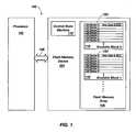
- FIG. 1is a simplified diagram of an embodiment of a system that incorporates a non-volatile memory device, in accordance with embodiments of the present invention.
- FIGS. 2A and 2Billustrate encoding of user data into blocks and sectors in a non-volatile memory array, in accordance with various embodiments of the present invention.
- FIG. 3is a memory map of a non-volatile memory array partitioned according to a file system, in accordance with various embodiments of the present invention.
- FIG. 4illustrates storage of an existing file stored in a file system.
- FIG. 5illustrates editing of an existing file in a file system.
- FIGS. 6A-6Dillustrate editing of an existing file in a file system, in accordance with an embodiment of the present invention.
- DOSdisk Operating System
- a DOS software-based systemstores and retrieves data based on these physical attributes.
- Magnetic hard disk drivesoperate by storing polarities on magnetic material. This material is able to be rewritten quickly and as often as desired. These characteristics allow DOS to develop a file structure that stores files at a given location, which is updated by a rewrite of that location as information is changed. Essentially all locations in DOS may be viewed as fixed and do not change over the life of the disk drive being used therewith, and are easily updated by rewrites of the smallest supported block of this structure.
- a sector(of a magnetic disk drive) is the smallest unit of storage that the DOS operating system supports.
- a logical block or sector(referred to herein as a logical block) has come to be defined as 512-bytes of information for DOS and most other operating systems in existence.
- Flash memoriessemiconductor non-volatile memory devices
- Flash and other non-volatile memory systemsthat emulate the storage characteristics of hard disk drives are preferably similarly structured to support storage in, by way of example and not limitation, 512-byte blocks along with additional storage for overhead associated with mass storage, such as ECC bits, status flags for the sector or erasable block, and/or redundant bits.
- the controller and/or software routinesadditionally allow the Flash memory device or a memory subsystem of Flash memory devices to appear as a read/write mass storage device (i.e., a magnetic disk) to the host by conforming the interface of the Flash memory device to be compatible with a standard interface for a conventional magnetic hard disk drive.
- a read/write mass storage devicei.e., a magnetic disk
- This approachallows the Flash memory device to appear to the operating system as a block read/write mass storage device or disk.
- Flash memoryincludes various known forms of non-volatile memory including without limitation NAND and NOR based non-volatile memory arrays.
- FIG. 1is a simplified diagram of an embodiment of an electronic system 100 that incorporates a Flash memory device 104 , in accordance with the present invention.
- the Flash memory 104is coupled to a processor 102 with an address/data bus 106 .
- a controller or a control state machine 110directs internal operation of the Flash memory device 104 , including managing the Flash memory array 108 .
- the Flash memory array 108contains floating gate memory cells arranged in a sequence of erasable blocks 116 , 118 .
- Electronic system 100may comprise, for example, computational and communication devices such as a computer, a cellular telephone, a personal digital assistant, an MP3 player, a digital camera, or other such devices that may find application to editing a stored file.
- all the cells in an erasable blockare generally erased all at once since a memory cell within an erasable block cannot be directly rewritten without first engaging in a block erase operation.
- the execution of erasable block managementis typically under the control of the internal controller or control state machine, an external memory controller, or software driver through a provided abstraction layer allowing the non-volatile device to appear as a freely rewriteable device.
- Other internal block management featuresinclude the logical address to physical address translation mapping with the translation layer, the assignment of erased and available erasable blocks for utilization, and scheduling for block erasure the erasable blocks that have been used and closed out.
- Erasable block managementmay also allow for load leveling of the internal floating gate memory cells to help prevent write fatigue failure.
- Write fatigueis where the floating gate memory cell, after repetitive writes and erasures, no longer properly erases and removes charge from the floating gate.
- Load leveling proceduresincrease the mean time between failure of the erasable block and non-volatile/Flash memory device as a whole.
- Flash memory array architecturesTwo common types of Flash memory array architectures are the “NAND” and “NOR” architectures.
- Other types of non-volatile memoryinclude, but are not limited to, Polymer Memory, Ferroelectric Random Access Memory (FeRAM), Ovionics Unified Memory (OUM), Nitride Read Only Memory (NROM), and Magnetoresistive Random Access Memory (MRAM).
- the floating gate memory cells of the memory arrayare arranged in a matrix.
- the gates of each floating gate memory cell of the array matrixare connected by rows to word select lines (word lines) and their drains are connected to column bit lines.
- the source of each floating gate memory cellis typically connected to a common source line.
- the NOR architecture floating gate memory arrayis accessed by a row decoder activating a row of floating gate memory cells by selecting the word line connected to their gates.
- the row of selected memory cellsthen place their stored data values on the column bit lines by flowing a differing current if in a programmed state or not programmed state from the connected source line to the connected column bit lines.
- a NAND Flash memory array architecturealso arranges its array of floating gate memory cells in a matrix such that the gates of each floating gate memory cell of the array are connected by rows to word lines. However each memory cell is not directly connected to a source line and a column bit line. Instead, the memory cells of the array are arranged together in strings, typically of 8, 16, 32 or more each, where the memory cells in the string are connected together in series, source to drain, between a common source line and a column bit line.
- the NAND architecture floating gate memory arrayis then accessed by a row decoder activating a row of floating gate memory cells by selecting the word select line connected to their gates. In addition, the word lines connected to the gates of the unselected memory cells of each string are also driven.
- the unselected memory cells of each stringare typically driven by a higher gate voltage so as to operate them as pass transistors and allowing them to pass current in a manner that is unrestricted by their stored data values.
- Currentthen flows from the source line to the column bit line through each floating gate memory cell of the series connected string, restricted only by the memory cells of each string that are selected to be read.
- the current encoded stored data values of the row of selected memory cellsare placed on the column bit lines.
- each erasable block 116 , 118contains a series of physical pages or rows 120 , each page containing physical storage for one or more logical sectors or blocks 124 (shown here for illustration purposes as a single logical sector/block 124 per physical page/row 120 ) that contain a user data space and a control/overhead data space.
- the overhead data spacecontains overhead information for operation of the logical block 124 , such as an error correction code (not shown), status flags, or an erasable block management data field area (not shown).
- the user data space in each logical block 124is typically 512 bytes long.
- Flash memory device 104may be incorporated into the system 100 as required.
- FIGS. 2A and 2Bdetail encoding 200 , 220 of user data into sector/logical blocks of a Flash memory array.
- user data 212 and header/overhead data 214are shown in a memory array 202 , which includes erasable blocks 116 , 118 ( FIG. 1 ), where a single 512-byte logical block is encoded in each physical page/row 210 of the memory array 202 .
- the memory array 202contains a series of rows 210 , each row containing a logical block having a user data area 204 and an overhead data area 206 .
- user data 226 and header/overhead data 228are shown in a memory array 222 , which includes erasable blocks 116 , 118 as illustrated in FIG. 1 , where multiple logical blocks 232 are encoded in each physical page/row 230 of the memory array 222 .
- many memoriessupport multiple logical sectors or logical block 232 within a single physical row page 230 .
- NAND architecture Flash memoriestypically utilize this approach due to their generally higher memory cell density and larger row page sizes.
- the memory row 230contains multiple logical blocks/sectors 232 , each logical block 232 having a user data area 226 and an overhead data/block header section 228 .
- the row page 230contains 2112 bytes of data (4 ⁇ 512 bytes user data+4 ⁇ 8 bytes ECC+32 bytes for overhead) and is formatted to contain four logical blocks 232 having a user data area 226 of 512-bytes each.
- the four logical sectors 232are typically sequentially addressed N, N+1, N+2, and N+3, where N is a base logical sector address for the row page 230 .
- Nis a base logical sector address for the row page 230 .
- the row pages 210 and 230 of FIGS. 2A and 2Bare for illustration purposes and that other row page sector formats of differing data sizes, numbers of logical blocks/sectors, and relative positioning of sectors are possible.
- the memory arrayis divided into a plurality of individually erasable groups of memory cells called erasable blocks, which are each typically further divided into a plurality of 512-byte physical blocks.
- the non-volatile memoryis formatted to conform to the data structures and management data fields/tables of the file system or memory structure being represented.
- Each physical block of the memory arrayalso may contain a header or overhead data area that typically includes various data used in the management of the physical block. This management data can include such items as the status of the physical block (valid, erased/available, or to be erased/invalid) and an error correction code (ECC) for the data of the logical block.
- the headertypically also includes an identifier that identifies the logical block address for the physical block.
- the translation layerin conjunction with the erasable block management (not shown) manages the storage of logical blocks in non-volatile memory devices or a non-volatile memory subsystem.
- the client of a translation layeris typically the file system or operating system of an associated host system or processor.
- the translation layer(not shown) allows the non-volatile memory to appear as a freely rewriteable device or magnetic disk/hard drive, allowing the client to read and write logical blocks to the non-volatile memory.
- FIG. 3is a memory map of a Flash memory array partitioned according to a file system, in accordance with one or more of the various embodiments of the present invention.
- a Flash memory arraymay be partitioned into one or more partitions.
- a single partition 126is illustrated and includes a system area 128 and a data area 130 .
- System area 128has various segments including, for example, the master boot record (“MBR”) area 132 , partition boot record (“PBR”) area 134 , FAT1 area 136 , FAT2 area 138 and root directory area 140 .
- MLRmaster boot record
- PBRpartition boot record
- MBR area 132stores overall partition information, including instructions to jump from MBR area 132 to PBR area 134 if the media is a bootable device.
- MBR area 132may also include a hidden area that is a reserved space (not shown) between MBR area 132 and PBR area 134 .
- PBR area 134includes partition/boot information for a partition.
- PBR area 134includes information for the type of FAT (for e.g., FAT12/16/32 bits depending on the FAT standard implemented, such as, respectively, FAT12, FAT16 or FAT32) a label (i.e., name of the drive), size of the drive; cluster size (i.e., the number of sectors per allocation unit) number of FAT areas (e.g., FAT 1 area and FAT 2 area) and the number of sectors per FAT.
- type of FATfor e.g., FAT12/16/32 bits depending on the FAT standard implemented, such as, respectively, FAT12, FAT16 or FAT32
- a labeli.e., name of the drive
- size of the drivesize of the drive
- cluster sizei.e., the number of sectors per allocation unit
- number of FAT arease.g., FAT 1 area and FAT 2 area
- FAT1 and FAT2 areas 136 , 138contain cluster information for each file.
- each entry in FAT1 and FAT2 areas 136 and 138contains 12 bits and there are a total of 4096 entries.
- Cluster 0 and 1are reserved for 0xFFFFF8 (for media type) and End of Cluster.
- a particular cluster(for e.g., cluster 4087 ) is used to indicate bad clusters.
- each entrycontains 16 bits and, for example, in a FAT32 file system, each entry contains 32 bits.
- Root directory area 140contains entries for each file.
- Each directory entryincludes a certain number of bytes for file name or directory (for e.g., 8 bytes), a number of bytes for extension (for e.g., 3 bytes), a number of bytes (for e.g., 1 byte) for file attributes (for e.g., if a file is read only, hidden, system file, volume label, directory or modified), a number of bytes indicating the time and date when a file was created, a certain number of bytes (for e.g., 2) for a starting cluster, and a certain number of bytes (for e.g., 4) indicating the file length.
- a certain number of bytes for file name or directoryfor e.g., 8 bytes
- a number of bytes for extensionfor e.g., 3 bytes
- a number of bytesfor e.g., 1 byte
- file attributesfor e.g., if a file is
- the number of bytes for the starting cluster points to the first cluster in the FAT and the last clustermay be indicated by 0xFFF, 0xFFFF or 0xFFFFFF.
- the host systemfinds free cluster space in FAT1 area 136 and data is written in data area 130 , including erasable blocks 116 , 118 ( FIG. 1 ). Entries in both the FAT1 area 136 and the FAT2 area 138 are then updated.
- the directory entry(e.g., the date/time/starting cluster/file length) is also updated.
- the root directory area 140is a table of, for example, 32-byte entries that each set forth certain attributes of a file.
- each directory entry making up the root directory in the root directory area 140includes a file name, a file extension, attribute flags, time and date stamps for the file, the starting cluster number for the clusters that make up the file, and the file size.
- Each file on the Flash memory device 104( FIG. 1 ) is made up of one or more clusters.
- the file allocation table (FAT) located in the FAT1 and FAT2 areas 136 , 138contains a record in the form of a chain identifying how the clusters making up the file are linked together.
- a typical FATcontains a list of two-byte entries, one for each cluster. For some prior FATs, the FAT entries are longer than two bytes. The length of each FAT entry depends upon the total number of clusters.
- the directory entry in the root directory area 140 for a filecontains the starting cluster number for that file, and the host system, such as processor 102 of FIG. 1 , uses that starting cluster number to access the FAT.
- Each FAT entryis a pointer to the next cluster of the file.
- the FAT entry retrieved by a first accesscontains the cluster number of the next cluster making up the file.
- the host systemsuch as processor 102 of FIG. 1 , uses that next cluster number to access the FAT to retrieve yet another cluster number, and continues this process until the end of the file is reached.
- Flash memory array 108When a file is being written or programmed into Flash memory array 108 ( FIG. 1 ), there exists an opportunity for the power to the memory device to be interrupted, resulting in an incomplete record of the chain of clusters identifying the file. While such interruptions may be reduced by physical locks or other preventive mechanisms, such mechanisms defeat the desirable portability and ease of configurability of Flash memory devices.
- the various embodiments of the present inventionprovide a mechanism to reduce the window of opportunity for creating errors in the chain of cluster as recorded in the FAT during an update or edit to an existing file.
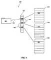
- FIGS. 4 and 5illustrate an edit to an existing file in accordance with a file system.
- FIG. 4illustrates an existing file 402 stored in a file system 400 .
- an indicia of an existing file 402is stored in the root directory area 140 of the system area 128 as described with respect to FIG. 3 .
- Included in the root directory area 140may be a file name, a file extension, attribute flags, time and date stamps for the file, the file size, and the starting cluster number or pointer 412 for the clusters that make up the file 402 .
- a location 406 in the FAT 404is pointed to by the root directory entry for the file 402 .
- Location 406corresponds to a cluster sector page 408 (used herein interchangeably depending upon the specific defined structure of the file system 400 ) of erasable block 410 .
- Location 406 in the FAT 404further includes a next cluster number or pointer 414 , which corresponds, by way of example, to cluster 416 of erasable block 418 .
- a location 420 in the FAT 404is pointed to by the next cluster number or pointer 414 for the file 402 .
- Location 420corresponds to a cluster 416 of erasable block 418 .
- Location 420 in the FAT 404further includes a next cluster number or pointer 422 , which corresponds, by way of example, to cluster 424 of erasable block 426 .
- a location 428 in the FAT 404includes an end-of-file indicator indicating that no more clusters are to be included in the file 402 .
- file 402includes clusters 408 , 416 , 424 from, for example, the respective erasable blocks 410 , 418 , 426 .
- FIG. 5illustrates an edit or update occurring to a file, illustrated as edited file 402 ′. It is recalled that the clusters or pages of the non-volatile memories as described herein are not rewriteable until the entire erasable block has been reclaimed by erasing or resetting the non-volatile memory cells within the block. Accordingly, FIG. 5 illustrates an edit to cluster 408 in file system 400 ′, which is rewritten at a new location in the Flash memory array as cluster 408 ′ in the erasable block 410 ′.
- the edited file 402 ′is correctly composed of clusters 408 ′, 416 , 424 ; however, FAT 404 has not yet been updated by redirecting starting cluster or pointer number 412 from pointing to location 406 to location 430 to reflect the relocation of amended cluster 408 ′ in erasable block 410 ′. If power to the memory device is interrupted prior to the completion of the change to the FAT, the edited file 402 ′ may become corrupt and unusable.
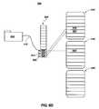
- FIGS. 6A-6Dillustrate an editing process of a file in a Flash memory device, in accordance with an embodiment of the present invention.
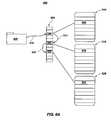
- FIG. 6Aillustrates an edit to an existing file in a file system.
- An existing file 502is stored in a file system 500 .
- an indicia of an existing file 502is stored in the root directory area 140 of the system area 128 as described with respect to FIG. 3 .
- Included in the root directory area 140may be a file name, a file extension, attribute flags, time and date stamps for the file, the file size, and the starting cluster number or pointer 512 for the clusters that make up the file 502 .
- a location 506 in the FAT 504is pointed to by the root directory entry for the file 502 .
- Location 506corresponds to a cluster sector page 508 (used herein interchangeably depending upon the specific defined structure of the file system 500 ) of erasable block 510 .
- Location 506 in the FAT 504further includes a next cluster number or pointer 514 , which corresponds, by way of example, to cluster 516 of erasable block 518 .
- a location 520 in the FAT 504is pointed to by the next cluster number or pointer 514 for the file 502 .
- Location 520corresponds to a cluster 516 of erasable block 518 .
- Location 520 in the FAT 504further includes a next cluster number or pointer 522 , which corresponds, by way of example, to cluster 524 of erasable block 526 .
- a location 528 in the FAT 504includes the last cluster in response to the end of the file 502 .
- file 502includes clusters 508 , 516 , 524 from, for example, the respective erasable blocks 510 , 518 , 526 .
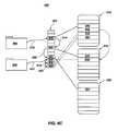
- FIG. 6Billustrates a further act in the editing of a file, in accordance with an embodiment of the present invention.
- a copy 602 of existing file 502 to be editedis created leaving the original unedited file 502 and the corresponding respective FAT entries intact during the editing process.
- the copy 602is stored in a file system 500 .
- a location 606 in the FAT 504is pointed to by a starting cluster number 612 for the file 602 .
- Location 606corresponds to a cluster sector page 608 of erasable block 510 .
- Location 606 in the FAT 504further includes a next cluster number or pointer 614 , which corresponds, by way of example, to cluster 616 of erasable block 510 .
- a location 620 in the FAT 504is pointed to by the next cluster number or pointer 614 for the file copy 602 .
- Location 620corresponds to a cluster 616 of erasable block 510 .
- Location 620 in the FAT 504further includes a next cluster number or pointer 622 , which corresponds, by way of example, to cluster 624 of erasable block 510 .
- a location 628 in the FAT 504includes an end-of-file indicator indicating that no more clusters are to be included in the file copy 602 .
- file copy 602includes clusters 608 , 616 , 624 from, for example, the erasable block 510 . It should be noted that the locations of the clusters within specific erasable blocks is merely illustrative and other arrangements are also contemplated.
- FIG. 6Cillustrates a further act in the editing of a file, in accordance with an embodiment of the present invention.
- the editsare performed on the file copy 602 .
- the clusters or pages of the non-volatile memories as described hereinare not rewriteable until the entire erasable block has been reclaimed by erasing or resetting the non-volatile memory cells within the block.
- one or more of the clusters 608 , 616 , 624 associated with the file copyare altered.
- the data in a cluster 608which is the copy of cluster 508 , is subjected to alterations.
- the altered datais written into cluster 608 ′ in the erasable block 518 . It is noted that the edited file copy 602 ′ is correctly composed of clusters 608 ′, 616 , 624 .
- one of the vulnerabilities of editing files in Flash memory devicesis the untimely interruption of power to the memory device prior to all of the entries in the file allocation table being correctly written or prior to all of the clusters associated with the edited file being correctly written into the Flash memory array.
- the occurrence of a power interruption during either the creation of the file copy 602 , or the editing of data stored in cluster 608 ′, or the reassociation of the location (e.g., location 606 from cluster 608 to cluster 608 ′) of the next cluster in the file allocation tablewould not result in the corruption of the original file 502 even though the edits may have been lost.
- the various embodiments of the present inventionnarrow the window of vulnerability of the files being corrupted during inadvertent power interruption by performing the editing on a copy of the original file while maintaining the root directory and FAT pointing to the original file in the Flash memory array. Should power interruption occur in any of these states, the original file remains uncorrupted on power up.
- the starting cluster number or pointer 512 in the root directory entry for file 502is reconfigured to point to location 606 in the FAT 504 .
- the window of vulnerability of corruption of a file stored in the Flash memory arrayhas, thus, been greatly narrowed down to power interruption occurring during the reconfiguration of the addressing of the single starting cluster in the root directory rather than during either the writing of data into clusters in the Flash memory array or the updating of the FAT.
Landscapes
- Engineering & Computer Science (AREA)
- Theoretical Computer Science (AREA)
- Physics & Mathematics (AREA)
- General Engineering & Computer Science (AREA)
- General Physics & Mathematics (AREA)
- Data Mining & Analysis (AREA)
- Databases & Information Systems (AREA)
- Human Computer Interaction (AREA)
- Quality & Reliability (AREA)
- Computer Security & Cryptography (AREA)
- Techniques For Improving Reliability Of Storages (AREA)
- Information Retrieval, Db Structures And Fs Structures Therefor (AREA)
Abstract
Description
Claims (27)
Priority Applications (5)
| Application Number | Priority Date | Filing Date | Title |
|---|---|---|---|
| US11/725,879US7917479B2 (en) | 2007-03-20 | 2007-03-20 | Non-volatile memory devices, systems including same and associated methods |
| PCT/US2008/057461WO2008115970A2 (en) | 2007-03-20 | 2008-03-19 | Non-volatile memory devices, systems including same and associated methods |
| US13/043,968US8655927B2 (en) | 2007-03-20 | 2011-03-09 | Memory device, electronic system, and methods associated with modifying data and a file of a memory device |
| US14/182,845US9075814B2 (en) | 2007-03-20 | 2014-02-18 | Memory device, electronic system, and methods associated with modifying data and a file of a memory device |
| US14/791,956US10037153B2 (en) | 2007-03-20 | 2015-07-06 | Memory device, electronic system, and methods associated with modifying data and a file of a memory device |
Applications Claiming Priority (1)
| Application Number | Priority Date | Filing Date | Title |
|---|---|---|---|
| US11/725,879US7917479B2 (en) | 2007-03-20 | 2007-03-20 | Non-volatile memory devices, systems including same and associated methods |
Related Child Applications (1)
| Application Number | Title | Priority Date | Filing Date |
|---|---|---|---|
| US13/043,968ContinuationUS8655927B2 (en) | 2007-03-20 | 2011-03-09 | Memory device, electronic system, and methods associated with modifying data and a file of a memory device |
Publications (2)
| Publication Number | Publication Date |
|---|---|
| US20080235486A1 US20080235486A1 (en) | 2008-09-25 |
| US7917479B2true US7917479B2 (en) | 2011-03-29 |
Family
ID=39766742
Family Applications (4)
| Application Number | Title | Priority Date | Filing Date |
|---|---|---|---|
| US11/725,879Active2028-10-07US7917479B2 (en) | 2007-03-20 | 2007-03-20 | Non-volatile memory devices, systems including same and associated methods |
| US13/043,968ActiveUS8655927B2 (en) | 2007-03-20 | 2011-03-09 | Memory device, electronic system, and methods associated with modifying data and a file of a memory device |
| US14/182,845ActiveUS9075814B2 (en) | 2007-03-20 | 2014-02-18 | Memory device, electronic system, and methods associated with modifying data and a file of a memory device |
| US14/791,956Active2028-02-05US10037153B2 (en) | 2007-03-20 | 2015-07-06 | Memory device, electronic system, and methods associated with modifying data and a file of a memory device |
Family Applications After (3)
| Application Number | Title | Priority Date | Filing Date |
|---|---|---|---|
| US13/043,968ActiveUS8655927B2 (en) | 2007-03-20 | 2011-03-09 | Memory device, electronic system, and methods associated with modifying data and a file of a memory device |
| US14/182,845ActiveUS9075814B2 (en) | 2007-03-20 | 2014-02-18 | Memory device, electronic system, and methods associated with modifying data and a file of a memory device |
| US14/791,956Active2028-02-05US10037153B2 (en) | 2007-03-20 | 2015-07-06 | Memory device, electronic system, and methods associated with modifying data and a file of a memory device |
Country Status (2)
| Country | Link |
|---|---|
| US (4) | US7917479B2 (en) |
| WO (1) | WO2008115970A2 (en) |
Cited By (2)
| Publication number | Priority date | Publication date | Assignee | Title |
|---|---|---|---|---|
| US20110179216A1 (en)* | 2010-01-20 | 2011-07-21 | Silicon Motion, Inc. | Data Storage Device and Data Access Method |
| US9075814B2 (en) | 2007-03-20 | 2015-07-07 | Micron Technology, Inc. | Memory device, electronic system, and methods associated with modifying data and a file of a memory device |
Families Citing this family (17)
| Publication number | Priority date | Publication date | Assignee | Title |
|---|---|---|---|---|
| US8429331B2 (en)* | 2008-12-03 | 2013-04-23 | Texas Instruments Incorporated | Storage optimizations by directory compaction in a fat file system |
| US8452934B2 (en)* | 2008-12-16 | 2013-05-28 | Sandisk Technologies Inc. | Controlled data access to non-volatile memory |
| TWI395100B (en)* | 2009-01-13 | 2013-05-01 | Innostor Technology Corp | Method for processing data of flash memory by separating levels and flash memory device thereof |
| CN102314490B (en)* | 2011-08-16 | 2013-07-10 | 晨星软件研发(深圳)有限公司 | Method and device for recovering Linux FAT (File Allocation Table) file system |
| TWI454912B (en)* | 2012-01-06 | 2014-10-01 | Phison Electronics Corp | Data processing method, memory controller and memory storage device |
| US10013322B2 (en)* | 2013-06-03 | 2018-07-03 | Hitachi, Ltd. | Storage apparatus and storage apparatus control method |
| TWI498732B (en)* | 2014-02-20 | 2015-09-01 | Phison Electronics Corp | Data transmitting method, memory control circuit unit and memory storage apparatus |
| TWI502345B (en)* | 2014-05-12 | 2015-10-01 | Via Tech Inc | Flash memory control chip and data storage device and flash memory control method |
| CN104462999B (en)* | 2014-12-12 | 2018-01-12 | 北京航星科技有限公司 | FAT32 file system data encryption methods |
| JP5974133B1 (en)* | 2015-03-20 | 2016-08-23 | 株式会社東芝 | Memory system |
| US10180788B2 (en)* | 2016-04-06 | 2019-01-15 | Sandisk Technologies Inc. | Data storage device having internal tagging capabilities |
| CN107229540A (en)* | 2017-06-06 | 2017-10-03 | 贵州易鲸捷信息技术有限公司 | A kind of database restoring method and system based on time point |
| WO2019148497A1 (en)* | 2018-02-05 | 2019-08-08 | 华为技术有限公司 | Date query method and device |
| US11016686B2 (en)* | 2019-09-18 | 2021-05-25 | Wolly Inc. | Apparatus and method of bad location management for storage class memory using distributed pointers |
| CN116775264A (en)* | 2022-03-11 | 2023-09-19 | 华为技术有限公司 | Process management method and electronic equipment |
| US12112052B2 (en) | 2022-03-30 | 2024-10-08 | Micron Technology, Inc. | Reading a master boot record for a namespace after reformatting the namespace |
| US12423008B2 (en) | 2022-04-21 | 2025-09-23 | Micron Technology, Inc. | Reading a master boot record for a namespace using a regular read operation |
Citations (32)
| Publication number | Priority date | Publication date | Assignee | Title |
|---|---|---|---|---|
| EP0444544A2 (en) | 1990-03-02 | 1991-09-04 | Fujitsu Limited | Updating or restoring method for stored data groups and system executing same |
| US5592669A (en)* | 1990-12-31 | 1997-01-07 | Intel Corporation | File structure for a non-volatile block-erasable semiconductor flash memory |
| US5630093A (en)* | 1990-12-31 | 1997-05-13 | Intel Corporation | Disk emulation for a non-volatile semiconductor memory utilizing a mapping table |
| US5983240A (en)* | 1995-12-15 | 1999-11-09 | Microsoft Corporation | Method and system of converting data from a source file system to a target file system |
| US6192376B1 (en) | 1998-11-13 | 2001-02-20 | International Business Machines Corporation | Method and apparatus for shadowing a hierarchical file system index structure to enable error recovery |
| US6275804B1 (en)* | 1996-08-21 | 2001-08-14 | Grundig Ag | Process and circuit arrangement for storing dictations in a digital dictating machine |
| US6704852B2 (en) | 2001-11-16 | 2004-03-09 | Key Technology Corporation | Control device applicable to flash memory card and method for building partial lookup table |
| US20040250172A1 (en)* | 2002-10-22 | 2004-12-09 | Microsoft Corporation | Transaction-safe FAT file system improvements |
| US20050055532A1 (en) | 2003-09-05 | 2005-03-10 | James Yu | Method for efficiently controlling read/write of flash memory |
| US20050108491A1 (en) | 2003-11-17 | 2005-05-19 | Micron Technology, Inc. | Method for testing flash memory power loss recovery |
| US6910054B1 (en)* | 1999-08-16 | 2005-06-21 | International Business Machines Corporation | Methods, systems and computer program products for storing data using a rolling window file |
| US6930503B2 (en) | 1997-08-21 | 2005-08-16 | Micron Technology, Inc. | System for testing integrated circuit devices |
| US6968439B2 (en) | 2002-08-29 | 2005-11-22 | Micron Technology, Inc. | Single segment data object management |
| US20050273648A1 (en) | 2000-07-06 | 2005-12-08 | Sreenath Mambakkam | Field-operable, stand-alone apparatus for media recovery and regeneration |
| US20060015676A1 (en) | 2004-07-15 | 2006-01-19 | Hiromichi Oribe | Semiconductor storage device |
| US20060044934A1 (en)* | 2004-09-02 | 2006-03-02 | Micron Technology, Inc. | Cluster based non-volatile memory translation layer |
| US20060047920A1 (en) | 2004-08-24 | 2006-03-02 | Matrix Semiconductor, Inc. | Method and apparatus for using a one-time or few-time programmable memory with a host device designed for erasable/rewriteable memory |
| US20060075395A1 (en) | 2004-10-01 | 2006-04-06 | Lee Charles C | Flash card system |
| US20060117072A1 (en)* | 2004-11-30 | 2006-06-01 | Mckenney Paul E | Cluster-wide read-copy update system and method |
| US7062606B2 (en) | 2002-11-01 | 2006-06-13 | Infineon Technologies Ag | Multi-threaded embedded processor using deterministic instruction memory to guarantee execution of pre-selected threads during blocking events |
| US7085908B2 (en)* | 2002-08-29 | 2006-08-01 | Micron Technology, Inc. | Linear object management for a range of flash memory |
| US20060184723A1 (en) | 2005-02-16 | 2006-08-17 | Sinclair Alan W | Direct file data programming and deletion in flash memories |
| US7130979B2 (en) | 2002-08-29 | 2006-10-31 | Micron Technology, Inc. | Dynamic volume management |
| US7139896B2 (en) | 2002-08-29 | 2006-11-21 | Micron Technology, Inc. | Linear and non-linear object management |
| US20060271725A1 (en) | 2005-05-24 | 2006-11-30 | Micron Technology, Inc. | Version based non-volatile memory translation layer |
| US20060282644A1 (en) | 2005-06-08 | 2006-12-14 | Micron Technology, Inc. | Robust index storage for non-volatile memory |
| US20070002612A1 (en) | 2005-06-29 | 2007-01-04 | Chang Robert C | Method and system for managing partitions in a storage device |
| US20070005560A1 (en) | 2005-07-01 | 2007-01-04 | Dan Dodge | Optimized startup verification of file system integrity |
| US7162606B2 (en) | 2002-08-29 | 2007-01-09 | Micron Technology, Inc. | Multiple segment data object management |
| US20070299888A1 (en)* | 2006-06-27 | 2007-12-27 | Microsoft Corporation | Automatically maintaining metadata in a file backup system |
| US7536507B1 (en)* | 2006-03-30 | 2009-05-19 | Emc Corporation | Methods, systems, and computer program products for preserving atomic writes using leaves and bitmaps |
| US7613738B2 (en)* | 2007-01-16 | 2009-11-03 | Microsoft Corporation | FAT directory structure for use in transaction safe file system |
Family Cites Families (3)
| Publication number | Priority date | Publication date | Assignee | Title |
|---|---|---|---|---|
| KR100484147B1 (en)* | 2002-07-26 | 2005-04-18 | 삼성전자주식회사 | Flash memory management method |
| US7747664B2 (en)* | 2007-01-16 | 2010-06-29 | Microsoft Corporation | Storage system format for transaction safe file system |
| US7917479B2 (en) | 2007-03-20 | 2011-03-29 | Micron Technology, Inc. | Non-volatile memory devices, systems including same and associated methods |
- 2007
- 2007-03-20USUS11/725,879patent/US7917479B2/enactiveActive
- 2008
- 2008-03-19WOPCT/US2008/057461patent/WO2008115970A2/enactiveApplication Filing
- 2011
- 2011-03-09USUS13/043,968patent/US8655927B2/enactiveActive
- 2014
- 2014-02-18USUS14/182,845patent/US9075814B2/enactiveActive
- 2015
- 2015-07-06USUS14/791,956patent/US10037153B2/enactiveActive
Patent Citations (32)
| Publication number | Priority date | Publication date | Assignee | Title |
|---|---|---|---|---|
| EP0444544A2 (en) | 1990-03-02 | 1991-09-04 | Fujitsu Limited | Updating or restoring method for stored data groups and system executing same |
| US5592669A (en)* | 1990-12-31 | 1997-01-07 | Intel Corporation | File structure for a non-volatile block-erasable semiconductor flash memory |
| US5630093A (en)* | 1990-12-31 | 1997-05-13 | Intel Corporation | Disk emulation for a non-volatile semiconductor memory utilizing a mapping table |
| US5983240A (en)* | 1995-12-15 | 1999-11-09 | Microsoft Corporation | Method and system of converting data from a source file system to a target file system |
| US6275804B1 (en)* | 1996-08-21 | 2001-08-14 | Grundig Ag | Process and circuit arrangement for storing dictations in a digital dictating machine |
| US6930503B2 (en) | 1997-08-21 | 2005-08-16 | Micron Technology, Inc. | System for testing integrated circuit devices |
| US6192376B1 (en) | 1998-11-13 | 2001-02-20 | International Business Machines Corporation | Method and apparatus for shadowing a hierarchical file system index structure to enable error recovery |
| US6910054B1 (en)* | 1999-08-16 | 2005-06-21 | International Business Machines Corporation | Methods, systems and computer program products for storing data using a rolling window file |
| US20050273648A1 (en) | 2000-07-06 | 2005-12-08 | Sreenath Mambakkam | Field-operable, stand-alone apparatus for media recovery and regeneration |
| US6704852B2 (en) | 2001-11-16 | 2004-03-09 | Key Technology Corporation | Control device applicable to flash memory card and method for building partial lookup table |
| US7085908B2 (en)* | 2002-08-29 | 2006-08-01 | Micron Technology, Inc. | Linear object management for a range of flash memory |
| US6968439B2 (en) | 2002-08-29 | 2005-11-22 | Micron Technology, Inc. | Single segment data object management |
| US7162606B2 (en) | 2002-08-29 | 2007-01-09 | Micron Technology, Inc. | Multiple segment data object management |
| US7139896B2 (en) | 2002-08-29 | 2006-11-21 | Micron Technology, Inc. | Linear and non-linear object management |
| US7130979B2 (en) | 2002-08-29 | 2006-10-31 | Micron Technology, Inc. | Dynamic volume management |
| US20040250172A1 (en)* | 2002-10-22 | 2004-12-09 | Microsoft Corporation | Transaction-safe FAT file system improvements |
| US7062606B2 (en) | 2002-11-01 | 2006-06-13 | Infineon Technologies Ag | Multi-threaded embedded processor using deterministic instruction memory to guarantee execution of pre-selected threads during blocking events |
| US20050055532A1 (en) | 2003-09-05 | 2005-03-10 | James Yu | Method for efficiently controlling read/write of flash memory |
| US20050108491A1 (en) | 2003-11-17 | 2005-05-19 | Micron Technology, Inc. | Method for testing flash memory power loss recovery |
| US20060015676A1 (en) | 2004-07-15 | 2006-01-19 | Hiromichi Oribe | Semiconductor storage device |
| US20060047920A1 (en) | 2004-08-24 | 2006-03-02 | Matrix Semiconductor, Inc. | Method and apparatus for using a one-time or few-time programmable memory with a host device designed for erasable/rewriteable memory |
| US20060044934A1 (en)* | 2004-09-02 | 2006-03-02 | Micron Technology, Inc. | Cluster based non-volatile memory translation layer |
| US20060075395A1 (en) | 2004-10-01 | 2006-04-06 | Lee Charles C | Flash card system |
| US20060117072A1 (en)* | 2004-11-30 | 2006-06-01 | Mckenney Paul E | Cluster-wide read-copy update system and method |
| US20060184723A1 (en) | 2005-02-16 | 2006-08-17 | Sinclair Alan W | Direct file data programming and deletion in flash memories |
| US20060271725A1 (en) | 2005-05-24 | 2006-11-30 | Micron Technology, Inc. | Version based non-volatile memory translation layer |
| US20060282644A1 (en) | 2005-06-08 | 2006-12-14 | Micron Technology, Inc. | Robust index storage for non-volatile memory |
| US20070002612A1 (en) | 2005-06-29 | 2007-01-04 | Chang Robert C | Method and system for managing partitions in a storage device |
| US20070005560A1 (en) | 2005-07-01 | 2007-01-04 | Dan Dodge | Optimized startup verification of file system integrity |
| US7536507B1 (en)* | 2006-03-30 | 2009-05-19 | Emc Corporation | Methods, systems, and computer program products for preserving atomic writes using leaves and bitmaps |
| US20070299888A1 (en)* | 2006-06-27 | 2007-12-27 | Microsoft Corporation | Automatically maintaining metadata in a file backup system |
| US7613738B2 (en)* | 2007-01-16 | 2009-11-03 | Microsoft Corporation | FAT directory structure for use in transaction safe file system |
Non-Patent Citations (2)
| Title |
|---|
| International Search Report for PCT/US2008/057461, dated Nov. 5, 2009, three (3) pages. |
| Written Opinion of the International Search Authority, dated Nov. 5, 2009, six (6) pages. |
Cited By (4)
| Publication number | Priority date | Publication date | Assignee | Title |
|---|---|---|---|---|
| US9075814B2 (en) | 2007-03-20 | 2015-07-07 | Micron Technology, Inc. | Memory device, electronic system, and methods associated with modifying data and a file of a memory device |
| US10037153B2 (en) | 2007-03-20 | 2018-07-31 | Micron Technology, Inc. | Memory device, electronic system, and methods associated with modifying data and a file of a memory device |
| US20110179216A1 (en)* | 2010-01-20 | 2011-07-21 | Silicon Motion, Inc. | Data Storage Device and Data Access Method |
| US8341378B2 (en)* | 2010-01-20 | 2012-12-25 | Silicon Motion, Inc. | Data storage device and data access method |
Also Published As
| Publication number | Publication date |
|---|---|
| US20140164445A1 (en) | 2014-06-12 |
| US20150324142A1 (en) | 2015-11-12 |
| WO2008115970A2 (en) | 2008-09-25 |
| US8655927B2 (en) | 2014-02-18 |
| US9075814B2 (en) | 2015-07-07 |
| US20080235486A1 (en) | 2008-09-25 |
| US20110161613A1 (en) | 2011-06-30 |
| US10037153B2 (en) | 2018-07-31 |
| WO2008115970A3 (en) | 2010-01-07 |
Similar Documents
| Publication | Publication Date | Title |
|---|---|---|
| US10037153B2 (en) | Memory device, electronic system, and methods associated with modifying data and a file of a memory device | |
| US8595424B2 (en) | Cluster based non-volatile memory translation layer | |
| US7944748B2 (en) | Erase block data splitting | |
| US9548108B2 (en) | Virtual memory device (VMD) application/driver for enhanced flash endurance | |
| US7350044B2 (en) | Data move method and apparatus | |
| JP4058322B2 (en) | Memory card | |
| US8954654B2 (en) | Virtual memory device (VMD) application/driver with dual-level interception for data-type splitting, meta-page grouping, and diversion of temp files to ramdisks for enhanced flash endurance | |
| JP4787266B2 (en) | Scratch pad block | |
| US7734891B2 (en) | Robust index storage for non-volatile memory | |
| US7752381B2 (en) | Version based non-volatile memory translation layer | |
| US7389397B2 (en) | Method of storing control information in a large-page flash memory device | |
| US7818492B2 (en) | Source and shadow wear-leveling method and apparatus | |
| US20100191897A1 (en) | System and method for wear leveling in a data storage device | |
| US20050138271A1 (en) | Rotational use of memory to minimize write cycles | |
| CN101408864B (en) | Data protection method for power failure and controller using the method | |
| JP2008112455A (en) | Memory card |
Legal Events
| Date | Code | Title | Description |
|---|---|---|---|
| AS | Assignment | Owner name:MICRON TECHNOLOGY, INC., IDAHO Free format text:ASSIGNMENT OF ASSIGNORS INTEREST;ASSIGNOR:SEPULVEDA, FRANK J.;REEL/FRAME:019089/0673 Effective date:20070309 | |
| FEPP | Fee payment procedure | Free format text:PAYOR NUMBER ASSIGNED (ORIGINAL EVENT CODE: ASPN); ENTITY STATUS OF PATENT OWNER: LARGE ENTITY | |
| STCF | Information on status: patent grant | Free format text:PATENTED CASE | |
| FPAY | Fee payment | Year of fee payment:4 | |
| AS | Assignment | Owner name:U.S. BANK NATIONAL ASSOCIATION, AS COLLATERAL AGENT, CALIFORNIA Free format text:SECURITY INTEREST;ASSIGNOR:MICRON TECHNOLOGY, INC.;REEL/FRAME:038669/0001 Effective date:20160426 Owner name:U.S. BANK NATIONAL ASSOCIATION, AS COLLATERAL AGEN Free format text:SECURITY INTEREST;ASSIGNOR:MICRON TECHNOLOGY, INC.;REEL/FRAME:038669/0001 Effective date:20160426 | |
| AS | Assignment | Owner name:MORGAN STANLEY SENIOR FUNDING, INC., AS COLLATERAL AGENT, MARYLAND Free format text:PATENT SECURITY AGREEMENT;ASSIGNOR:MICRON TECHNOLOGY, INC.;REEL/FRAME:038954/0001 Effective date:20160426 Owner name:MORGAN STANLEY SENIOR FUNDING, INC., AS COLLATERAL Free format text:PATENT SECURITY AGREEMENT;ASSIGNOR:MICRON TECHNOLOGY, INC.;REEL/FRAME:038954/0001 Effective date:20160426 | |
| AS | Assignment | Owner name:U.S. BANK NATIONAL ASSOCIATION, AS COLLATERAL AGENT, CALIFORNIA Free format text:CORRECTIVE ASSIGNMENT TO CORRECT THE REPLACE ERRONEOUSLY FILED PATENT #7358718 WITH THE CORRECT PATENT #7358178 PREVIOUSLY RECORDED ON REEL 038669 FRAME 0001. ASSIGNOR(S) HEREBY CONFIRMS THE SECURITY INTEREST;ASSIGNOR:MICRON TECHNOLOGY, INC.;REEL/FRAME:043079/0001 Effective date:20160426 Owner name:U.S. BANK NATIONAL ASSOCIATION, AS COLLATERAL AGEN Free format text:CORRECTIVE ASSIGNMENT TO CORRECT THE REPLACE ERRONEOUSLY FILED PATENT #7358718 WITH THE CORRECT PATENT #7358178 PREVIOUSLY RECORDED ON REEL 038669 FRAME 0001. ASSIGNOR(S) HEREBY CONFIRMS THE SECURITY INTEREST;ASSIGNOR:MICRON TECHNOLOGY, INC.;REEL/FRAME:043079/0001 Effective date:20160426 | |
| AS | Assignment | Owner name:JPMORGAN CHASE BANK, N.A., AS COLLATERAL AGENT, ILLINOIS Free format text:SECURITY INTEREST;ASSIGNORS:MICRON TECHNOLOGY, INC.;MICRON SEMICONDUCTOR PRODUCTS, INC.;REEL/FRAME:047540/0001 Effective date:20180703 Owner name:JPMORGAN CHASE BANK, N.A., AS COLLATERAL AGENT, IL Free format text:SECURITY INTEREST;ASSIGNORS:MICRON TECHNOLOGY, INC.;MICRON SEMICONDUCTOR PRODUCTS, INC.;REEL/FRAME:047540/0001 Effective date:20180703 | |
| AS | Assignment | Owner name:MICRON TECHNOLOGY, INC., IDAHO Free format text:RELEASE BY SECURED PARTY;ASSIGNOR:U.S. BANK NATIONAL ASSOCIATION, AS COLLATERAL AGENT;REEL/FRAME:047243/0001 Effective date:20180629 | |
| MAFP | Maintenance fee payment | Free format text:PAYMENT OF MAINTENANCE FEE, 8TH YEAR, LARGE ENTITY (ORIGINAL EVENT CODE: M1552); ENTITY STATUS OF PATENT OWNER: LARGE ENTITY Year of fee payment:8 | |
| AS | Assignment | Owner name:MICRON TECHNOLOGY, INC., IDAHO Free format text:RELEASE BY SECURED PARTY;ASSIGNOR:MORGAN STANLEY SENIOR FUNDING, INC., AS COLLATERAL AGENT;REEL/FRAME:050937/0001 Effective date:20190731 | |
| AS | Assignment | Owner name:MICRON TECHNOLOGY, INC., IDAHO Free format text:RELEASE BY SECURED PARTY;ASSIGNOR:JPMORGAN CHASE BANK, N.A., AS COLLATERAL AGENT;REEL/FRAME:051028/0001 Effective date:20190731 Owner name:MICRON SEMICONDUCTOR PRODUCTS, INC., IDAHO Free format text:RELEASE BY SECURED PARTY;ASSIGNOR:JPMORGAN CHASE BANK, N.A., AS COLLATERAL AGENT;REEL/FRAME:051028/0001 Effective date:20190731 | |
| MAFP | Maintenance fee payment | Free format text:PAYMENT OF MAINTENANCE FEE, 12TH YEAR, LARGE ENTITY (ORIGINAL EVENT CODE: M1553); ENTITY STATUS OF PATENT OWNER: LARGE ENTITY Year of fee payment:12 |