US7916295B2 - Alignment mark and method of getting position reference for wafer - Google Patents
Alignment mark and method of getting position reference for waferDownload PDFInfo
- Publication number
- US7916295B2 US7916295B2US12/203,310US20331008AUS7916295B2US 7916295 B2US7916295 B2US 7916295B2US 20331008 AUS20331008 AUS 20331008AUS 7916295 B2US7916295 B2US 7916295B2
- Authority
- US
- United States
- Prior art keywords
- pattern
- block
- alignment mark
- dense
- adjacent
- Prior art date
- Legal status (The legal status is an assumption and is not a legal conclusion. Google has not performed a legal analysis and makes no representation as to the accuracy of the status listed.)
- Expired - Fee Related, expires
Links
Images


Classifications
- H—ELECTRICITY
- H01—ELECTRIC ELEMENTS
- H01L—SEMICONDUCTOR DEVICES NOT COVERED BY CLASS H10
- H01L23/00—Details of semiconductor or other solid state devices
- H01L23/544—Marks applied to semiconductor devices or parts, e.g. registration marks, alignment structures, wafer maps
- G—PHYSICS
- G03—PHOTOGRAPHY; CINEMATOGRAPHY; ANALOGOUS TECHNIQUES USING WAVES OTHER THAN OPTICAL WAVES; ELECTROGRAPHY; HOLOGRAPHY
- G03F—PHOTOMECHANICAL PRODUCTION OF TEXTURED OR PATTERNED SURFACES, e.g. FOR PRINTING, FOR PROCESSING OF SEMICONDUCTOR DEVICES; MATERIALS THEREFOR; ORIGINALS THEREFOR; APPARATUS SPECIALLY ADAPTED THEREFOR
- G03F9/00—Registration or positioning of originals, masks, frames, photographic sheets or textured or patterned surfaces, e.g. automatically
- G03F9/70—Registration or positioning of originals, masks, frames, photographic sheets or textured or patterned surfaces, e.g. automatically for microlithography
- G03F9/7073—Alignment marks and their environment
- G03F9/7076—Mark details, e.g. phase grating mark, temporary mark
- G—PHYSICS
- G03—PHOTOGRAPHY; CINEMATOGRAPHY; ANALOGOUS TECHNIQUES USING WAVES OTHER THAN OPTICAL WAVES; ELECTROGRAPHY; HOLOGRAPHY
- G03F—PHOTOMECHANICAL PRODUCTION OF TEXTURED OR PATTERNED SURFACES, e.g. FOR PRINTING, FOR PROCESSING OF SEMICONDUCTOR DEVICES; MATERIALS THEREFOR; ORIGINALS THEREFOR; APPARATUS SPECIALLY ADAPTED THEREFOR
- G03F9/00—Registration or positioning of originals, masks, frames, photographic sheets or textured or patterned surfaces, e.g. automatically
- G03F9/70—Registration or positioning of originals, masks, frames, photographic sheets or textured or patterned surfaces, e.g. automatically for microlithography
- G03F9/7073—Alignment marks and their environment
- G03F9/7084—Position of mark on substrate, i.e. position in (x, y, z) of mark, e.g. buried or resist covered mark, mark on rearside, at the substrate edge, in the circuit area, latent image mark, marks in plural levels
- H—ELECTRICITY
- H01—ELECTRIC ELEMENTS
- H01L—SEMICONDUCTOR DEVICES NOT COVERED BY CLASS H10
- H01L2223/00—Details relating to semiconductor or other solid state devices covered by the group H01L23/00
- H01L2223/544—Marks applied to semiconductor devices or parts
- H01L2223/54426—Marks applied to semiconductor devices or parts for alignment
- H—ELECTRICITY
- H01—ELECTRIC ELEMENTS
- H01L—SEMICONDUCTOR DEVICES NOT COVERED BY CLASS H10
- H01L2223/00—Details relating to semiconductor or other solid state devices covered by the group H01L23/00
- H01L2223/544—Marks applied to semiconductor devices or parts
- H01L2223/54453—Marks applied to semiconductor devices or parts for use prior to dicing
- H01L2223/54466—Located in a dummy or reference die
- H—ELECTRICITY
- H01—ELECTRIC ELEMENTS
- H01L—SEMICONDUCTOR DEVICES NOT COVERED BY CLASS H10
- H01L2924/00—Indexing scheme for arrangements or methods for connecting or disconnecting semiconductor or solid-state bodies as covered by H01L24/00
- H01L2924/0001—Technical content checked by a classifier
- H01L2924/0002—Not covered by any one of groups H01L24/00, H01L24/00 and H01L2224/00
Definitions
- This inventionrelates to IC fabricating processes, and more particularly relates to an alignment mark, and a method of getting a position reference for a wafer that is based on the alignment mark.
- a wafer for IC fabricationusually requires a position reference to be defined thereon before subjected to a process, such as a checking process like overlay checking process.
- a position referenceis often got by forming two alignment marks in the pre-layer at different positions and locating the alignment marks as two reference points.
- FIG. 1illustrates a prior-art alignment mark 100 on a wafer 10 , which serves as one of two reference points 12 on the wafer 10 and includes an L-shaped pattern 110 and its surrounding 120 .
- the alignment mark 100is located by detecting brightness difference between the L-shaped pattern 110 and its surrounding 120 .
- the contrast between the L-shaped pattern 110 and its surrounding 120is insufficient, so that the alignment mark 100 is difficult to locate and the recipe cannot be setup.
- the contrastcan be increased by using near-IR light in the detection, additional tools for manipulating the near-IR detection are required.
- this inventionprovides an alignment mark, which has a higher contrast facilitating its locating so that the recipe can be setup readily.
- This inventionalso provides a method of getting a position reference for a wafer, which is based on the alignment mark of this invention.
- An alignment mark of the inventionincludes at least one dense pattern and at least one block-like pattern adjacent thereto, and is shown as at least one dark image and at least one bright image adjacent thereto.
- the method of getting a position reference for a waferis described below.
- An alignment mark of this inventionis formed.
- the alignment markwhich is shown as at least one dark image and at least one bright image adjacent thereto that are formed by the at least one dense pattern and the at least one block-like pattern, is then detected.
- the methodmay be applied to a checking process of the wafer, such as an overlay checking process.
- the at least one dense patternincludes an array pattern.
- the array patternmay include a plurality of parallel linear patterns, wherein each linear pattern may have an x-directional orientation or y-directional orientation.
- the array patternmay have only one pitch, or have two or more pitches.
- the array patternmay include a one-dimensional (1D) array pattern or a 2D array pattern.
- the at least one dense pattern and at least one block-like patternmay be formed from a portion of a pre-layer, or formed as openings in a portion of the pre-layer. It is also possible that at least one of the at least one dense pattern and the at least one block-like pattern has an irregular shape.
- the at least one block-like patternmay include a single block pattern, or include two or more neighboring block patterns.
- the alignment mark of the inventionis shown as at least one dark image and at least one bright image adjacent thereto as detected in visible light, and thus has a high contrast and can be located easily in visible light for the recipe setup. Hence, no additional tool for manipulating near-IR detection is required, and an opaque layer is allowed to be included in the film stack.
- FIG. 1illustrates a prior-art alignment mark on a wafer.
- FIG. 2Aillustrates an alignment mark according to a first embodiment of this invention as well as its use in a method of getting a position reference for a wafer according to the first embodiment of this invention.
- FIG. 2Billustrates another alignment mark according to the first embodiment of this invention.
- FIGS. 3A-3Billustrate two alignment marks according to a second embodiment of this invention.
- FIGS. 4A-4Billustrate two alignment marks according to a third embodiment of this invention.
- FIG. 5illustrates an alignment mark according to a fourth embodiment of this invention.
- FIG. 6illustrates an alignment mark according to a fifth embodiment of this invention.
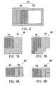
- FIGS. 7A-7Billustrate two alignment marks according to a sixth embodiment of this invention.
- FIGS. 8A-8Billustrate two alignment marks according to a seventh embodiment of this invention.
- the dense patterns of the alignment marks in the following embodiments of this inventionare all array patterns
- the dense pattern of this inventioncan be other types of pattern, such as a rectangular spiral pattern or a pattern including a plurality of concentric rectangular rings.
- FIG. 2Aillustrates an alignment mark according to the first embodiment of this invention as well as its use in a method of getting a position reference for a wafer according to the first embodiment.
- the alignment mark 200includes an array pattern 210 as a dense pattern and a single block pattern 220 as a block-like pattern that are formed from the pre-layer.
- the array pattern 210includes a plurality of parallel linear patterns having only one pitch, wherein each linear pattern has a y-directional orientation. As detected in visible light, the array pattern 210 is shown as a dark image 21 and the block pattern 220 is shown as a bright image 22 in the detector 20 of the alignment tool (not shown), so the alignment mark 200 has a high contrast and can be easily located on the wafer 10 to serve as a position reference.
- the alignment toolmay be one used in a wafer checking process, such as an overlay checking process.
- the overlay checking machine usedmay be one of the KLA-Tencor series, which is equipped with a overlay metrology tool as an alignment tool utilizing visible light for an alignment action.
- FIG. 2Billustrates another alignment mark according to the first embodiment.
- the alignment mark 200 ′is similar to that ( 200 ) in FIG. 2A except that the array pattern 210 ′ includes a plurality of parallel linear patterns each with an x-directional orientation.
- FIGS. 3A-3Billustrate two alignment marks according to the second embodiment of this invention where at least one of the array pattern and the block pattern has a number more than one.
- the alignment mark 300is derived from the alignment mark 200 in FIG. 2A by adding another block pattern 220 at the left side of the array pattern 210 adjacent to the array pattern 210 .
- the alignment mark of this embodimentmay include one array pattern 210 and a plurality of block patterns 220 adjacent thereto.
- the alignment markmay include one block pattern 220 and a plurality of array patterns 210 adjacent thereto.
- the alignment mark 300 ′is derived from the alignment mark 200 in FIG. 2A by adding another block pattern 220 at the upper side of the array pattern 210 adjacent to the array pattern 210 and adding another array pattern 210 at the upper side of the block pattern 220 adjacent to the block pattern 220 .
- the alignment markmay include a plurality of array patterns 210 and a plurality of block patterns 220 , wherein each array pattern 210 is adjacent to at least one block pattern 220 and each block pattern 220 is adjacent to at least one array pattern 210 .
- the array pattern as a dense patternis not limited to have only one pitch, and may have two or more pitches.
- FIGS. 4A-4Billustrate two such alignment marks according to the third embodiment of this invention.
- the alignment mark 400 in FIG. 4Aincludes an array pattern 410 having two pitches and a single block pattern 420 like the above block pattern 220 .
- the alignment mark 400 ′ in FIG. 4Bincludes an array pattern 410 ′ having more than two pitches and a block pattern 420 .
- the array pattern as a dense patternis not limited to be a 1D array pattern, and may be a 2D array pattern.
- FIG. 5illustrates such an alignment mark according to the fourth embodiment of this invention.
- the alignment mark 500 in FIG. 5includes a 2D array pattern 510 and a single block pattern 520 adjacent thereto.
- FIG. 6illustrates such an alignment mark 600 according to the fifth embodiment of this invention, which includes a single block pattern 620 as a wide opening in a portion of the pre-layer and an array pattern 610 including a plurality of y-orientation trenches in the portion of the pre-layer.
- the alignment mark 600is exactly in the inverse tone of the alignment mark 200 in FIG. 2A .
- each of the array pattern and the block patternis not limited to have a regular shape like a rectangular or square shape, and at least one of the array pattern and the block pattern may have an irregular shape.
- FIGS. 7A-7Billustrate two such alignment marks according to the sixth embodiment of this invention.
- the alignment mark 700includes an array pattern 710 with a regular (rectangular or square) shape and a single block pattern 720 with an irregular shape adjacent to two neighboring sides of the array pattern 710 .
- the alignment mark 700 ′ in FIG. 7Bincludes an array pattern 710 ′ with an irregular shape and a single block pattern 720 ′ also with an irregular shape.
- the block-like pattern of the alignment mark of this inventionis not limited to include a single block pattern, but may alternatively include two or more neighboring block patterns.
- FIGS. 8A-8Billustrate two such alignment marks according to the seventh embodiment of this invention.
- the alignment mark 800includes an array pattern 810 as a dense pattern and a block-like pattern 820 including two neighboring block patterns.
- the alignment mark 800 ′ in FIG. 8Bincludes an array pattern 810 and a block-like pattern 820 ′ including three neighboring block patterns.
- the alignment markmay include a 2D array pattern and a block-like pattern including two or more block patterns, wherein the 2D array pattern have two or more pitches and the 2D array pattern and the block patterns are all formed as openings in the pre-layer.
- the alignment mark of the inventionis shown as at least one dark image and at least one bright image adjacent thereto as detected in visible light, and thus has a high contrast and can be located easily in visible light for the recipe setup.
Landscapes
- Physics & Mathematics (AREA)
- General Physics & Mathematics (AREA)
- Condensed Matter Physics & Semiconductors (AREA)
- Engineering & Computer Science (AREA)
- Computer Hardware Design (AREA)
- Microelectronics & Electronic Packaging (AREA)
- Power Engineering (AREA)
- Exposure Of Semiconductors, Excluding Electron Or Ion Beam Exposure (AREA)
- Exposure And Positioning Against Photoresist Photosensitive Materials (AREA)
- Container, Conveyance, Adherence, Positioning, Of Wafer (AREA)
Abstract
Description
Claims (26)
Priority Applications (2)
| Application Number | Priority Date | Filing Date | Title |
|---|---|---|---|
| US12/203,310US7916295B2 (en) | 2008-09-03 | 2008-09-03 | Alignment mark and method of getting position reference for wafer |
| TW097146768ATWI487002B (en) | 2008-09-03 | 2008-12-02 | Method of aligning marks and obtaining a position reference point of a wafer |
Applications Claiming Priority (1)
| Application Number | Priority Date | Filing Date | Title |
|---|---|---|---|
| US12/203,310US7916295B2 (en) | 2008-09-03 | 2008-09-03 | Alignment mark and method of getting position reference for wafer |
Publications (2)
| Publication Number | Publication Date |
|---|---|
| US20100053616A1 US20100053616A1 (en) | 2010-03-04 |
| US7916295B2true US7916295B2 (en) | 2011-03-29 |
Family
ID=41724977
Family Applications (1)
| Application Number | Title | Priority Date | Filing Date |
|---|---|---|---|
| US12/203,310Expired - Fee RelatedUS7916295B2 (en) | 2008-09-03 | 2008-09-03 | Alignment mark and method of getting position reference for wafer |
Country Status (2)
| Country | Link |
|---|---|
| US (1) | US7916295B2 (en) |
| TW (1) | TWI487002B (en) |
Families Citing this family (6)
| Publication number | Priority date | Publication date | Assignee | Title |
|---|---|---|---|---|
| EP2410406A1 (en)* | 2010-07-23 | 2012-01-25 | Anoto AB | Display with coding pattern |
| CN102540737B (en)* | 2010-12-14 | 2013-12-11 | 无锡华润上华半导体有限公司 | Photomask for photoetching machine testing and testing method of photoetching machine |
| TWI588932B (en)* | 2015-05-29 | 2017-06-21 | Wafer positioning identification device and method thereof | |
| JP6595870B2 (en)* | 2015-09-30 | 2019-10-23 | 株式会社Screenホールディングス | Correction information generating apparatus, drawing apparatus, correction information generating method, and drawing method |
| CN114200796B (en)* | 2020-09-02 | 2024-01-26 | 中芯国际集成电路制造(上海)有限公司 | Alignment mark and forming method thereof |
| JP2023043534A (en)* | 2021-09-16 | 2023-03-29 | キオクシア株式会社 | Measuring method, measuring apparatus, and mark |
Citations (15)
| Publication number | Priority date | Publication date | Assignee | Title |
|---|---|---|---|---|
| US5294975A (en)* | 1992-10-15 | 1994-03-15 | Altera Corporation | Laser alignment target for semiconductor integrated circuits |
| US5528372A (en)* | 1990-03-12 | 1996-06-18 | Fujitsu Limited | Alignment mark, laser trimmer and semiconductor device manufacturing process |
| US6778275B2 (en)* | 2002-02-20 | 2004-08-17 | Micron Technology, Inc. | Aberration mark and method for estimating overlay error and optical aberrations |
| US20040185637A1 (en)* | 2003-03-20 | 2004-09-23 | Taiwan Semiconductor Manufacturing Co., Ltd., | Method to preserve alignment mark optical integrity |
| US20050097764A1 (en) | 2003-11-10 | 2005-05-12 | Kim Su H. | Enhanced visibility of overlay measurement marks |
| US6940609B2 (en) | 2001-08-08 | 2005-09-06 | Nova Measuring Instruments, Ltd. | Method and system for measuring the topography of a sample |
| US20070187606A1 (en) | 2005-11-18 | 2007-08-16 | Kla-Tencor Technologies Corporation | Overlay metrology using the near infra-red spectral range |
| US7288848B2 (en)* | 2003-11-24 | 2007-10-30 | Samsung Electronics Co., Ltd. | Overlay mark for measuring and correcting alignment errors |
| US20080106738A1 (en)* | 2006-11-03 | 2008-05-08 | Samsung Electronics Co., Ltd. | Alignment mark |
| US7408642B1 (en)* | 2006-02-17 | 2008-08-05 | Kla-Tencor Technologies Corporation | Registration target design for managing both reticle grid error and wafer overlay |
| US7440105B2 (en)* | 2002-12-05 | 2008-10-21 | Kla-Tencor Technologies Corporation | Continuously varying offset mark and methods of determining overlay |
| US20090096116A1 (en)* | 2007-10-16 | 2009-04-16 | Macronix International Co., Ltd. | Alignment mark and mehtod for forming the same |
| US20090225331A1 (en)* | 2008-03-04 | 2009-09-10 | Asml Netherlands B.V. | Method of Providing Alignment Marks, Device Manufacturing Method and Lithographic Apparatus |
| US20090246709A1 (en)* | 2008-03-25 | 2009-10-01 | Tetsuro Nakasugi | Manufacturing method of semiconductor device |
| US7684040B2 (en)* | 2007-06-07 | 2010-03-23 | Macronix International Co., Ltd. | Overlay mark and application thereof |
Family Cites Families (64)
| Publication number | Priority date | Publication date | Assignee | Title |
|---|---|---|---|---|
| US3660605A (en)* | 1970-04-15 | 1972-05-02 | Int Standard Electric Corp | Pulse code modulation switching system utilizing tasi |
| US4047157A (en)* | 1974-02-01 | 1977-09-06 | Digital Equipment Corporation | Secondary storage facility for data processing |
| FR2618624B1 (en)* | 1987-07-24 | 1992-04-30 | Michel Servel | HYBRID TIME MULTIPLEX SWITCHING SYSTEM WITH OPTIMIZED BUFFER MEMORY |
| US5596331A (en)* | 1988-05-13 | 1997-01-21 | Lockheed Martin Corporation | Real-time control sequencer with state matrix logic |
| EP0444315B1 (en)* | 1990-02-26 | 1997-10-01 | Digital Equipment Corporation | System and method for software application event collection |
| DE69513300T2 (en)* | 1994-08-29 | 2000-03-23 | Torsana A/S, Skodsborg | DETERMINATION PROCEDURE |
| US5912887A (en)* | 1996-06-27 | 1999-06-15 | Mciworldcom, Inc. | System and method for implementing user-to-user data transfer services |
| US6098033A (en)* | 1997-07-31 | 2000-08-01 | Microsoft Corporation | Determining similarity between words |
| US6282544B1 (en)* | 1999-05-24 | 2001-08-28 | Computer Associates Think, Inc. | Method and apparatus for populating multiple data marts in a single aggregation process |
| US6163774A (en)* | 1999-05-24 | 2000-12-19 | Platinum Technology Ip, Inc. | Method and apparatus for simplified and flexible selection of aggregate and cross product levels for a data warehouse |
| WO2001008041A1 (en)* | 1999-07-21 | 2001-02-01 | Mindpass A/S | Method and systems for making olap hierarchies summarisable |
| WO2001042937A1 (en)* | 1999-12-06 | 2001-06-14 | Henry Milan | Modular stackable component system including universal serial bus hub |
| US20010034679A1 (en)* | 2000-01-21 | 2001-10-25 | Wrigley Mark L. | Platform independent and non-invasive financial report mark-up |
| US20020029207A1 (en)* | 2000-02-28 | 2002-03-07 | Hyperroll, Inc. | Data aggregation server for managing a multi-dimensional database and database management system having data aggregation server integrated therein |
| US6662192B1 (en)* | 2000-03-29 | 2003-12-09 | Bizrate.Com | System and method for data collection, evaluation, information generation, and presentation |
| US7376573B1 (en)* | 2000-04-28 | 2008-05-20 | Accenture Llp | Claims data analysis toolkit |
| US20020004390A1 (en)* | 2000-05-05 | 2002-01-10 | Cutaia Rory Joseph | Method and system for managing telecommunications services and network interconnections |
| NZ522305A (en)* | 2000-05-22 | 2004-04-30 | Nero Res Oy | Method in monitoring the condition of machines |
| US7133858B1 (en)* | 2000-06-30 | 2006-11-07 | Microsoft Corporation | Partial pre-aggregation in relational database queries |
| US20020186818A1 (en)* | 2000-08-29 | 2002-12-12 | Osteonet, Inc. | System and method for building and manipulating a centralized measurement value database |
| US6687693B2 (en)* | 2000-12-18 | 2004-02-03 | Ncr Corporation | Architecture for distributed relational data mining systems |
| US7233998B2 (en)* | 2001-03-22 | 2007-06-19 | Sony Computer Entertainment Inc. | Computer architecture and software cells for broadband networks |
| US7191183B1 (en)* | 2001-04-10 | 2007-03-13 | Rgi Informatics, Llc | Analytics and data warehousing infrastructure and services |
| US20020161520A1 (en)* | 2001-04-27 | 2002-10-31 | International Business Machines Corporation | Method to display allowed parking areas in a vehicle |
| US7430532B2 (en)* | 2001-06-12 | 2008-09-30 | Blackrock Financial Management, Inc. | System and method for trade entry |
| JP4028844B2 (en)* | 2001-08-01 | 2007-12-26 | インターナショナル・ビジネス・マシーンズ・コーポレーション | Graphics image generating apparatus, method and program thereof |
| TW503479B (en)* | 2001-08-16 | 2002-09-21 | Mosel Vitelic Inc | Exposure time determination method of wafer photolithography process |
| US7437344B2 (en)* | 2001-10-01 | 2008-10-14 | L'oreal S.A. | Use of artificial intelligence in providing beauty advice |
| US20030088565A1 (en)* | 2001-10-15 | 2003-05-08 | Insightful Corporation | Method and system for mining large data sets |
| US20030149586A1 (en)* | 2001-11-07 | 2003-08-07 | Enkata Technologies | Method and system for root cause analysis of structured and unstructured data |
| US20030177055A1 (en)* | 2002-03-14 | 2003-09-18 | The Procter & Gamble Company | Virtual test market system and method |
| US7107285B2 (en)* | 2002-03-16 | 2006-09-12 | Questerra Corporation | Method, system, and program for an improved enterprise spatial system |
| US7483945B2 (en)* | 2002-04-19 | 2009-01-27 | Akamai Technologies, Inc. | Method of, and system for, webcasting with just-in-time resource provisioning, automated telephone signal acquisition and streaming, and fully-automated event archival |
| US20020194145A1 (en)* | 2002-05-28 | 2002-12-19 | Boucher Thomas Charles | Method and system for financing a renewable energy generating facility |
| US7023528B2 (en)* | 2002-06-10 | 2006-04-04 | International Business Machines Corporation | Hybrid electronic mask |
| US20040030593A1 (en)* | 2002-08-05 | 2004-02-12 | Webster Adam W. | On demand aircraft charter and air taxi booking and dispatch system |
| US7870148B2 (en)* | 2003-04-18 | 2011-01-11 | Unica Corporation | Scalable computation of data |
| US7516157B2 (en)* | 2003-05-08 | 2009-04-07 | Microsoft Corporation | Relational directory |
| ES2671059T3 (en)* | 2003-07-17 | 2018-06-04 | e-distribuzione S.p.A. | Procedure and system for remote meter updates to measure the consumption of electricity, water or gas |
| US7239989B2 (en)* | 2003-07-18 | 2007-07-03 | Oracle International Corporation | Within-distance query pruning in an R-tree index |
| US20050043097A1 (en)* | 2003-08-21 | 2005-02-24 | Spidermonk Entertainment, Llc | Interrelated game and information portals provided within the context of an encompassing virtual world |
| US7549145B2 (en)* | 2003-09-25 | 2009-06-16 | International Business Machines Corporation | Processor dedicated code handling in a multi-processor environment |
| US20050240085A1 (en)* | 2004-01-16 | 2005-10-27 | Basf Aktiengesellschaft | Balanced care product customization |
| US7650344B2 (en)* | 2004-02-09 | 2010-01-19 | Coremetrics, Inc. | System and method of managing software product-line customizations |
| US20090006156A1 (en)* | 2007-01-26 | 2009-01-01 | Herbert Dennis Hunt | Associating a granting matrix with an analytic platform |
| US20050216512A1 (en)* | 2004-03-26 | 2005-09-29 | Rahav Dor | Method of accessing a work of art, a product, or other tangible or intangible objects without knowing the title or name thereof using fractional sampling of the work of art or object |
| US7058544B2 (en)* | 2004-07-09 | 2006-06-06 | The United States Of America As Represented By The Secretary Of The Army | Knowledge-based condition survey inspection (KBCSI) framework and procedure |
| US7490009B2 (en)* | 2004-08-03 | 2009-02-10 | Fei Company | Method and system for spectroscopic data analysis |
| US7647328B2 (en)* | 2004-10-08 | 2010-01-12 | Sentillion, Inc. | Method and apparatus for processing a context change request in a CCOW environment |
| WO2007005909A2 (en)* | 2005-07-01 | 2007-01-11 | Fred Covely | Methods and apparatus for authentication of content delivery and playback applications |
| US20070061185A1 (en)* | 2005-09-09 | 2007-03-15 | International Business Machines Corporation | Method, system, and computer program product for implementing availability messaging services |
| US20070276676A1 (en)* | 2006-05-23 | 2007-11-29 | Christopher Hoenig | Social information system |
| US20080077469A1 (en)* | 2006-09-27 | 2008-03-27 | Philport Joseph C | Method and system for determining media exposure |
| US8160984B2 (en)* | 2007-01-26 | 2012-04-17 | Symphonyiri Group, Inc. | Similarity matching of a competitor's products |
| US20090006788A1 (en)* | 2007-01-26 | 2009-01-01 | Herbert Dennis Hunt | Associating a flexible data hierarchy with an availability condition in a granting matrix |
| US20080288522A1 (en)* | 2007-01-26 | 2008-11-20 | Herbert Dennis Hunt | Creating and storing a data field alteration datum using an analytic platform |
| US20080288209A1 (en)* | 2007-01-26 | 2008-11-20 | Herbert Dennis Hunt | Flexible projection facility within an analytic platform |
| WO2008092147A2 (en)* | 2007-01-26 | 2008-07-31 | Information Resources, Inc. | Analytic platform |
| US9390158B2 (en)* | 2007-01-26 | 2016-07-12 | Information Resources, Inc. | Dimensional compression using an analytic platform |
| US20080270363A1 (en)* | 2007-01-26 | 2008-10-30 | Herbert Dennis Hunt | Cluster processing of a core information matrix |
| US20090006309A1 (en)* | 2007-01-26 | 2009-01-01 | Herbert Dennis Hunt | Cluster processing of an aggregated dataset |
| US20080294372A1 (en)* | 2007-01-26 | 2008-11-27 | Herbert Dennis Hunt | Projection facility within an analytic platform |
| US20080294996A1 (en)* | 2007-01-31 | 2008-11-27 | Herbert Dennis Hunt | Customized retailer portal within an analytic platform |
| US20080228699A1 (en)* | 2007-03-16 | 2008-09-18 | Expanse Networks, Inc. | Creation of Attribute Combination Databases |
- 2008
- 2008-09-03USUS12/203,310patent/US7916295B2/ennot_activeExpired - Fee Related
- 2008-12-02TWTW097146768Apatent/TWI487002B/ennot_activeIP Right Cessation
Patent Citations (15)
| Publication number | Priority date | Publication date | Assignee | Title |
|---|---|---|---|---|
| US5528372A (en)* | 1990-03-12 | 1996-06-18 | Fujitsu Limited | Alignment mark, laser trimmer and semiconductor device manufacturing process |
| US5294975A (en)* | 1992-10-15 | 1994-03-15 | Altera Corporation | Laser alignment target for semiconductor integrated circuits |
| US6940609B2 (en) | 2001-08-08 | 2005-09-06 | Nova Measuring Instruments, Ltd. | Method and system for measuring the topography of a sample |
| US6778275B2 (en)* | 2002-02-20 | 2004-08-17 | Micron Technology, Inc. | Aberration mark and method for estimating overlay error and optical aberrations |
| US7440105B2 (en)* | 2002-12-05 | 2008-10-21 | Kla-Tencor Technologies Corporation | Continuously varying offset mark and methods of determining overlay |
| US20040185637A1 (en)* | 2003-03-20 | 2004-09-23 | Taiwan Semiconductor Manufacturing Co., Ltd., | Method to preserve alignment mark optical integrity |
| US20050097764A1 (en) | 2003-11-10 | 2005-05-12 | Kim Su H. | Enhanced visibility of overlay measurement marks |
| US7288848B2 (en)* | 2003-11-24 | 2007-10-30 | Samsung Electronics Co., Ltd. | Overlay mark for measuring and correcting alignment errors |
| US20070187606A1 (en) | 2005-11-18 | 2007-08-16 | Kla-Tencor Technologies Corporation | Overlay metrology using the near infra-red spectral range |
| US7408642B1 (en)* | 2006-02-17 | 2008-08-05 | Kla-Tencor Technologies Corporation | Registration target design for managing both reticle grid error and wafer overlay |
| US20080106738A1 (en)* | 2006-11-03 | 2008-05-08 | Samsung Electronics Co., Ltd. | Alignment mark |
| US7684040B2 (en)* | 2007-06-07 | 2010-03-23 | Macronix International Co., Ltd. | Overlay mark and application thereof |
| US20090096116A1 (en)* | 2007-10-16 | 2009-04-16 | Macronix International Co., Ltd. | Alignment mark and mehtod for forming the same |
| US20090225331A1 (en)* | 2008-03-04 | 2009-09-10 | Asml Netherlands B.V. | Method of Providing Alignment Marks, Device Manufacturing Method and Lithographic Apparatus |
| US20090246709A1 (en)* | 2008-03-25 | 2009-10-01 | Tetsuro Nakasugi | Manufacturing method of semiconductor device |
Also Published As
| Publication number | Publication date |
|---|---|
| US20100053616A1 (en) | 2010-03-04 |
| TW201011811A (en) | 2010-03-16 |
| TWI487002B (en) | 2015-06-01 |
Similar Documents
| Publication | Publication Date | Title |
|---|---|---|
| US10747123B2 (en) | Semiconductor device having overlay pattern | |
| US7916295B2 (en) | Alignment mark and method of getting position reference for wafer | |
| JP4926171B2 (en) | Apparatus and method for determining overlay of rotationally symmetric or mirror-symmetric objects | |
| US6484060B1 (en) | Layout for measurement of overlay error | |
| CN112447542B (en) | Semiconductor wafer inspection method and system | |
| JP3067732B2 (en) | Semiconductor device alignment device and alignment method | |
| KR102350548B1 (en) | Method of inspecting a wafer | |
| CN102486995B (en) | Dynamic Wafer Alignment Method and Exposure Scanning System | |
| US7211449B2 (en) | Enhanced uniqueness for pattern recognition | |
| US20090226078A1 (en) | Method and apparatus for aligning a substrate and for inspecting a pattern on a substrate | |
| CN102931114B (en) | A kind of crystal round test approach | |
| US9766559B2 (en) | Edge-dominant alignment method in exposure scanner system | |
| US20060121374A1 (en) | Method for determining pattern misalignment over a substrate | |
| CN104281010B (en) | forming method and substrate | |
| TWI820371B (en) | Inspection tool for use in lithographic device manufacturing processes and metrology method | |
| JP4525067B2 (en) | Misalignment detection mark | |
| US8729716B2 (en) | Alignment accuracy mark | |
| JP2007049074A (en) | Combined error measuring mark and method for manufacturing semiconductor device using same | |
| US20080185741A1 (en) | Semiconductor device having dummy pattern | |
| US8487644B2 (en) | Method and pattern carrier for optimizing inspection recipe of defect inspection tool | |
| KR100408722B1 (en) | Stepper alignment mark | |
| KR100713911B1 (en) | Miss alignment check method in laminated structure | |
| KR100642380B1 (en) | Wafer defect measurement method | |
| KR100896850B1 (en) | How to sort overlay keys | |
| JP2006108579A (en) | Dimension measuring method and semiconductor device manufacturing method |
Legal Events
| Date | Code | Title | Description |
|---|---|---|---|
| AS | Assignment | Owner name:MACRONIX INTERNATIONAL CO., LTD.,TAIWAN Free format text:ASSIGNMENT OF ASSIGNORS INTEREST;ASSIGNORS:YEH, CHIAO-WEN;HUANG, CHIH-HAO;REEL/FRAME:021477/0900 Effective date:20080805 Owner name:MACRONIX INTERNATIONAL CO., LTD., TAIWAN Free format text:ASSIGNMENT OF ASSIGNORS INTEREST;ASSIGNORS:YEH, CHIAO-WEN;HUANG, CHIH-HAO;REEL/FRAME:021477/0900 Effective date:20080805 | |
| STCF | Information on status: patent grant | Free format text:PATENTED CASE | |
| FPAY | Fee payment | Year of fee payment:4 | |
| MAFP | Maintenance fee payment | Free format text:PAYMENT OF MAINTENANCE FEE, 8TH YEAR, LARGE ENTITY (ORIGINAL EVENT CODE: M1552) Year of fee payment:8 | |
| FEPP | Fee payment procedure | Free format text:MAINTENANCE FEE REMINDER MAILED (ORIGINAL EVENT CODE: REM.); ENTITY STATUS OF PATENT OWNER: LARGE ENTITY | |
| LAPS | Lapse for failure to pay maintenance fees | Free format text:PATENT EXPIRED FOR FAILURE TO PAY MAINTENANCE FEES (ORIGINAL EVENT CODE: EXP.); ENTITY STATUS OF PATENT OWNER: LARGE ENTITY | |
| STCH | Information on status: patent discontinuation | Free format text:PATENT EXPIRED DUE TO NONPAYMENT OF MAINTENANCE FEES UNDER 37 CFR 1.362 | |
| FP | Lapsed due to failure to pay maintenance fee | Effective date:20230329 |