US7916180B2 - Simultaneous multiple field of view digital cameras - Google Patents
Simultaneous multiple field of view digital camerasDownload PDFInfo
- Publication number
- US7916180B2 US7916180B2US11/788,279US78827907AUS7916180B2US 7916180 B2US7916180 B2US 7916180B2US 78827907 AUS78827907 AUS 78827907AUS 7916180 B2US7916180 B2US 7916180B2
- Authority
- US
- United States
- Prior art keywords
- channel
- digital camera
- fov
- image sensor
- optics component
- Prior art date
- Legal status (The legal status is an assumption and is not a legal conclusion. Google has not performed a legal analysis and makes no representation as to the accuracy of the status listed.)
- Active, expires
Links
- 238000012545processingMethods0.000claimsabstractdescription63
- 238000000034methodMethods0.000claimsabstractdescription61
- 239000004065semiconductorSubstances0.000claimsabstractdescription26
- 239000000758substrateSubstances0.000claimsabstractdescription25
- 239000003086colorantSubstances0.000claimsdescription49
- 230000003287optical effectEffects0.000description77
- 238000003491arrayMethods0.000description65
- 238000010586diagramMethods0.000description25
- 230000010354integrationEffects0.000description18
- 230000008569processEffects0.000description18
- 238000004891communicationMethods0.000description14
- 238000003384imaging methodMethods0.000description14
- 238000001429visible spectrumMethods0.000description14
- 239000000463materialSubstances0.000description12
- 238000009500colour coatingMethods0.000description11
- 238000005516engineering processMethods0.000description10
- 230000002093peripheral effectEffects0.000description10
- 238000003860storageMethods0.000description9
- 238000000576coating methodMethods0.000description7
- 238000012546transferMethods0.000description7
- 230000008901benefitEffects0.000description6
- 238000001228spectrumMethods0.000description6
- 230000006870functionEffects0.000description5
- XUIMIQQOPSSXEZ-UHFFFAOYSA-NSiliconChemical compound[Si]XUIMIQQOPSSXEZ-UHFFFAOYSA-N0.000description4
- 239000011248coating agentSubstances0.000description4
- 239000004020conductorSubstances0.000description4
- 230000000694effectsEffects0.000description4
- 238000007689inspectionMethods0.000description4
- 238000004519manufacturing processMethods0.000description4
- 230000007246mechanismEffects0.000description4
- 230000035945sensitivityEffects0.000description4
- 238000000926separation methodMethods0.000description4
- 229910052710siliconInorganic materials0.000description4
- 239000010703siliconSubstances0.000description4
- 238000013461designMethods0.000description3
- 238000001514detection methodMethods0.000description3
- 239000000975dyeSubstances0.000description3
- 238000001914filtrationMethods0.000description3
- -1for exampleSubstances0.000description3
- 239000011159matrix materialSubstances0.000description3
- 229910044991metal oxideInorganic materials0.000description3
- 150000004706metal oxidesChemical class0.000description3
- 230000009467reductionEffects0.000description3
- 241000579895ChlorostilbonSpecies0.000description2
- RYGMFSIKBFXOCR-UHFFFAOYSA-NCopperChemical compound[Cu]RYGMFSIKBFXOCR-UHFFFAOYSA-N0.000description2
- 238000010521absorption reactionMethods0.000description2
- 230000008859changeEffects0.000description2
- 229910052876emeraldInorganic materials0.000description2
- 239000010976emeraldSubstances0.000description2
- 229910052732germaniumInorganic materials0.000description2
- GNPVGFCGXDBREM-UHFFFAOYSA-Ngermanium atomChemical compound[Ge]GNPVGFCGXDBREM-UHFFFAOYSA-N0.000description2
- 239000011521glassSubstances0.000description2
- 239000002184metalSubstances0.000description2
- 229910052751metalInorganic materials0.000description2
- 230000010287polarizationEffects0.000description2
- 230000004044responseEffects0.000description2
- 230000008685targetingEffects0.000description2
- 206010034960PhotophobiaDiseases0.000description1
- 239000000853adhesiveSubstances0.000description1
- 230000001070adhesive effectEffects0.000description1
- 230000003466anti-cipated effectEffects0.000description1
- 238000013459approachMethods0.000description1
- 230000000712assemblyEffects0.000description1
- 238000000429assemblyMethods0.000description1
- 230000004888barrier functionEffects0.000description1
- 230000003542behavioural effectEffects0.000description1
- 230000033228biological regulationEffects0.000description1
- 230000015572biosynthetic processEffects0.000description1
- 230000001413cellular effectEffects0.000description1
- 230000000295complement effectEffects0.000description1
- 239000002131composite materialSubstances0.000description1
- 150000001875compoundsChemical class0.000description1
- 238000004590computer programMethods0.000description1
- 238000011960computer-aided designMethods0.000description1
- 229920000547conjugated polymerPolymers0.000description1
- 229910052802copperInorganic materials0.000description1
- 239000010949copperSubstances0.000description1
- 239000011889copper foilSubstances0.000description1
- 238000012937correctionMethods0.000description1
- 239000006059cover glassSubstances0.000description1
- 230000007123defenseEffects0.000description1
- 230000002950deficientEffects0.000description1
- 230000001934delayEffects0.000description1
- 238000011982device technologyMethods0.000description1
- 230000003292diminished effectEffects0.000description1
- 230000002708enhancing effectEffects0.000description1
- 230000001815facial effectEffects0.000description1
- 239000000835fiberSubstances0.000description1
- 230000005669field effectEffects0.000description1
- 230000014509gene expressionEffects0.000description1
- 238000005286illuminationMethods0.000description1
- 230000008676importEffects0.000description1
- 238000010348incorporationMethods0.000description1
- 208000013469light sensitivityDiseases0.000description1
- 238000012986modificationMethods0.000description1
- 230000004048modificationEffects0.000description1
- 230000001537neural effectEffects0.000description1
- 230000035515penetrationEffects0.000description1
- 229920000642polymerPolymers0.000description1
- 238000005096rolling processMethods0.000description1
- 230000011664signalingEffects0.000description1
- 230000007704transitionEffects0.000description1
- 230000000007visual effectEffects0.000description1
Images


Classifications
- H—ELECTRICITY
- H10—SEMICONDUCTOR DEVICES; ELECTRIC SOLID-STATE DEVICES NOT OTHERWISE PROVIDED FOR
- H10F—INORGANIC SEMICONDUCTOR DEVICES SENSITIVE TO INFRARED RADIATION, LIGHT, ELECTROMAGNETIC RADIATION OF SHORTER WAVELENGTH OR CORPUSCULAR RADIATION
- H10F39/00—Integrated devices, or assemblies of multiple devices, comprising at least one element covered by group H10F30/00, e.g. radiation detectors comprising photodiode arrays
- H10F39/10—Integrated devices
- H10F39/12—Image sensors
- H10F39/18—Complementary metal-oxide-semiconductor [CMOS] image sensors; Photodiode array image sensors
- H10F39/182—Colour image sensors
- H—ELECTRICITY
- H04—ELECTRIC COMMUNICATION TECHNIQUE
- H04N—PICTORIAL COMMUNICATION, e.g. TELEVISION
- H04N23/00—Cameras or camera modules comprising electronic image sensors; Control thereof
- H04N23/45—Cameras or camera modules comprising electronic image sensors; Control thereof for generating image signals from two or more image sensors being of different type or operating in different modes, e.g. with a CMOS sensor for moving images in combination with a charge-coupled device [CCD] for still images
- H—ELECTRICITY
- H04—ELECTRIC COMMUNICATION TECHNIQUE
- H04N—PICTORIAL COMMUNICATION, e.g. TELEVISION
- H04N23/00—Cameras or camera modules comprising electronic image sensors; Control thereof
- H04N23/50—Constructional details
- H04N23/55—Optical parts specially adapted for electronic image sensors; Mounting thereof
- H—ELECTRICITY
- H04—ELECTRIC COMMUNICATION TECHNIQUE
- H04N—PICTORIAL COMMUNICATION, e.g. TELEVISION
- H04N25/00—Circuitry of solid-state image sensors [SSIS]; Control thereof
- H04N25/10—Circuitry of solid-state image sensors [SSIS]; Control thereof for transforming different wavelengths into image signals
- H04N25/11—Arrangement of colour filter arrays [CFA]; Filter mosaics
- H04N25/13—Arrangement of colour filter arrays [CFA]; Filter mosaics characterised by the spectral characteristics of the filter elements
- H04N25/133—Arrangement of colour filter arrays [CFA]; Filter mosaics characterised by the spectral characteristics of the filter elements including elements passing panchromatic light, e.g. filters passing white light
- H—ELECTRICITY
- H04—ELECTRIC COMMUNICATION TECHNIQUE
- H04N—PICTORIAL COMMUNICATION, e.g. TELEVISION
- H04N25/00—Circuitry of solid-state image sensors [SSIS]; Control thereof
- H04N25/40—Extracting pixel data from image sensors by controlling scanning circuits, e.g. by modifying the number of pixels sampled or to be sampled
- H04N25/41—Extracting pixel data from a plurality of image sensors simultaneously picking up an image, e.g. for increasing the field of view by combining the outputs of a plurality of sensors
- H—ELECTRICITY
- H04—ELECTRIC COMMUNICATION TECHNIQUE
- H04N—PICTORIAL COMMUNICATION, e.g. TELEVISION
- H04N5/00—Details of television systems
- H04N5/222—Studio circuitry; Studio devices; Studio equipment
- H04N5/262—Studio circuits, e.g. for mixing, switching-over, change of character of image, other special effects ; Cameras specially adapted for the electronic generation of special effects
- H04N5/2624—Studio circuits, e.g. for mixing, switching-over, change of character of image, other special effects ; Cameras specially adapted for the electronic generation of special effects for obtaining an image which is composed of whole input images, e.g. splitscreen
- H—ELECTRICITY
- H10—SEMICONDUCTOR DEVICES; ELECTRIC SOLID-STATE DEVICES NOT OTHERWISE PROVIDED FOR
- H10F—INORGANIC SEMICONDUCTOR DEVICES SENSITIVE TO INFRARED RADIATION, LIGHT, ELECTROMAGNETIC RADIATION OF SHORTER WAVELENGTH OR CORPUSCULAR RADIATION
- H10F77/00—Constructional details of devices covered by this subclass
- H10F77/40—Optical elements or arrangements
- H10F77/407—Optical elements or arrangements indirectly associated with the devices
- H—ELECTRICITY
- H10—SEMICONDUCTOR DEVICES; ELECTRIC SOLID-STATE DEVICES NOT OTHERWISE PROVIDED FOR
- H10F—INORGANIC SEMICONDUCTOR DEVICES SENSITIVE TO INFRARED RADIATION, LIGHT, ELECTROMAGNETIC RADIATION OF SHORTER WAVELENGTH OR CORPUSCULAR RADIATION
- H10F39/00—Integrated devices, or assemblies of multiple devices, comprising at least one element covered by group H10F30/00, e.g. radiation detectors comprising photodiode arrays
- H10F39/80—Constructional details of image sensors
- H10F39/805—Coatings
- H10F39/8053—Colour filters
- H—ELECTRICITY
- H10—SEMICONDUCTOR DEVICES; ELECTRIC SOLID-STATE DEVICES NOT OTHERWISE PROVIDED FOR
- H10F—INORGANIC SEMICONDUCTOR DEVICES SENSITIVE TO INFRARED RADIATION, LIGHT, ELECTROMAGNETIC RADIATION OF SHORTER WAVELENGTH OR CORPUSCULAR RADIATION
- H10F39/00—Integrated devices, or assemblies of multiple devices, comprising at least one element covered by group H10F30/00, e.g. radiation detectors comprising photodiode arrays
- H10F39/80—Constructional details of image sensors
- H10F39/806—Optical elements or arrangements associated with the image sensors
- H10F39/8063—Microlenses
Definitions
- the following disclosurerelates generally to optical devices and more particularly to digital imaging.
- zoomAs performed by the lens system, is known as “optical zoom”. This desirable “zoom lens” feature adds additional components, size and cost to a lens system.
- the zoom lensalso requires significant power and time to operate. The time to move the optical elements in the zoom lens limits the ability to acquire multiple fields of view in rapid and/or simultaneous fashion.
- Digital camera suppliershave one advantage over traditional film providers in the area of zoom capability.
- digital camerascan provide “electronic zoom” which provides the zoom capability by cropping the outer regions of an image and then electronically enlarging the center region to the original size of the image.
- electronic zoomprovides the zoom capability by cropping the outer regions of an image and then electronically enlarging the center region to the original size of the image.
- a degree of resolutionis lost when performing this process.
- digital camerascapture discrete input to form a picture rather than the ubiquitous process of film, the lost resolution is more pronounced.
- “electronic zoom”is a desired feature, it is not a direct substitute for “optical zoom.”
- Digital photographyoften requires imaging and subsequent display of different fields of views of the same or nearly the same scene. In some applications it is desirable to capture different fields of view of the same scene at the same time. This is not possible with optical zoom because of the time required to move the optical elements.
- Electronic zoomcan display wide and narrow field of view (FOV) by cropping and enlarging the size of a portion of an image, but the displayed narrow field is often of inferior resolution.
- Foveal image sensorsthat use multiple pixels arranged both within and about a central fovea region of the chip can be used to acquire both a wide and narrow field of view. The pixels in the central fovea region have a smaller size than the pixels arranged in peripheral rings about the central region. The foveal image sensor has high resolution only in the narrow field of view.
- FIG. 1is a block diagram of a conventional digital camera.
- FIG. 2Ashows the operation of conventional lens assembly in a retracted mode (also referred to as normal mode or a near focus setting).
- FIG. 2Bshows the operation of conventional lens assembly in an optical zoom mode (sometimes referred to as a far focus setting).
- FIG. 3shows a digital camera configured for simultaneous acquisition of multiple fields of view, under an embodiment.
- FIG. 4is a digital camera system that includes multiple camera channels, under an embodiment.
- FIG. 5is a flow diagram for simultaneous acquisition of multiple fields of view, under an embodiment.
- FIG. 6is a block diagram of a digital camera, under an embodiment.
- FIG. 7is an exploded view of a digital camera subsystem, under an embodiment.
- FIG. 8is a block diagram of a digital camera having a three array/lens configuration, under an embodiment.
- FIG. 9is a block diagram of a digital camera subsystem that employs separate arrays on one image sensor, under an embodiment.
- FIG. 10is a block diagram of arrays, each of which receives a respective color as passed by a respective lens, under an embodiment.
- FIG. 11is a block diagram of processing circuitry of a digital camera subsystem, under an embodiment.
- FIG. 12is a block diagram of signal processing circuitry, under an embodiment.
- FIG. 13is an exploded perspective view of a digital camera, under an embodiment.
- FIGS. 14A-14Dare schematic exploded representations of one embodiment of an optics portion, under an embodiment.
- FIGS. 15A-15Care schematic representations of a sensor array, under an embodiment.
- FIG. 16is a schematic cross-sectional view of a digital camera apparatus, under an embodiment.
- FIG. 17is a schematic perspective view of a digital camera apparatus having one or more optics portions with the capability to provide color separation, under an embodiment.
- FIG. 18Ais a block diagram of a processor of a digital camera subsystem, under an embodiment.
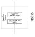
- FIG. 18Bis a block diagram of a channel processor of a digital camera subsystem, under an embodiment.
- FIG. 18Cis a block diagram of an image pipeline of a digital camera subsystem, under an embodiment.
- FIG. 18Dis a block diagram of an image post processor of a digital camera subsystem, under an embodiment.
- FIG. 19is a block diagram of digital camera system, including system control components, under an embodiment.
- a digital camera system and methodsare described below that provide a digital camera in which multiple fields of view (FOV) of an image are simultaneously acquired.
- the digital camera systemincludes a digital camera having two or more camera channels each with independent image sensors.
- the sensor of each camera channelhas an active area that includes multiple picture elements (pixels), and image capture includes simultaneous or nearly simultaneous use of the multiple camera channels.
- Each camera channel and associated optics of that camera channelhas a predetermined field of view that can be different from other camera channels of the digital camera system.
- the digital camera systemtherefore makes possible the formation of multiple high resolution images in which different fields of view are acquired simultaneously.
- the digital camera systemfurther includes methods for forming images as described below.
- the digital camera system of an embodimentincludes a multiple optical system configuration in which a scene is imaged onto multiple image sensors located on the same integrated circuit substrate. Each image sensor operates independently and, when combined with its own optics and electronics, forms a separate camera channel. Each image sensor is located beneath an optical assembly.
- the optical assemblyincluding optional mechanical or electromechanical mechanisms, can be processed on the image sensor wafer, applied to the image wafer by a separate wafer transfer, transferred individually by pick and place method, or attached at the die level.
- the combination of the focal plane or image sensor size along with the optical focal length associated with each image sensoris chosen to provide a desired field of view.
- the electrical operation of each camera channelis independent of the other camera channels and multiple fields of view can be acquired simultaneously.
- the pixel size, array size and image sensor configurationcan have approximately the same configuration in each camera channel or be configured so as to be optimized for each field of view.
- the imager electrical operationcan be similar in each camera channel or configured so as to be optimized for each field of view (such as imager frame rate and integration time).
- the multiple camera channelsoperate independently, however embodiments provide for sharing of electrical and/or mechanical components in a host digital camera.
- the digital camera systems described hereinenable visual imaging tasks including search, detection, recognition, and tracking, which may not be easily handled by conventional imaging systems with single optics.
- the digital camera systems of an embodimentcan be used in active vision systems of autonomous or semi-autonomous host systems. These systems range from commercial and industrial applications to surveillance and military applications.
- the commercial and industrial applicationsmay involve robots, unmanned vehicles, self-navigating cars, automatic assembly and product inspection systems.
- the surveillance and military applicationsmay involve iris and facial imaging, smart weapons and missile defense systems.
- the digital camera system of an embodimentimproves performance of imaging systems and improves functions of search, detection, recognition and tracking by providing simultaneous high resolution imaging in multiple fields of view with optimum electrical operation (such as independent frame rate and integration time control) in each field of view.
- FIG. 1is a block diagram of a conventional digital camera 100 .
- the digital camera 100includes a lens assembly 110 , a color filter array layer 112 , an image sensor 116 , and an electronic image storage media 120 .
- the digital camera 100also includes a power supply 124 , a peripheral user interface (represented as a shutter button) 132 , a circuit board 136 (which supports and electrically interconnects the aforementioned components), a housing 140 (including housing portions 141 , 142 , 143 , 144 , 145 and 146 ) and a shutter assembly (not shown), which controls an aperture 150 and passage of light into the digital camera 100 .
- a mechanical frame 164is used to couple or connect the various components or parts of the lens assembly 110 .
- the lens assembly 110includes lenses 161 and 162 and one or more electromechanical devices 163 to move the lenses 161 and 162 along a center axis 165 .
- the lenses 161 and 162may comprise multiple elements arranged together to form an integral optical component. Additional lenses may be included.
- the electromechanical device 163 of the lens assembly 110 and the mechanical frame 164 of the lens assembly 110can include numerous components and/or complex assemblies.
- the optional color filter array layer 112includes an array of color filters arranged in a Bayer pattern (e.g., a 2 ⁇ 2 matrix of colors with alternating red and green in one row and alternating green and blue in the other row, although other colors may be used).
- the Bayer pattern(often used in color camera applications) is repeated throughout the color filter array.
- the image sensor 116includes a plurality of identical photo detectors (sometimes referred to as “picture elements” or “pixels”) arranged in a matrix.
- the number of photo detectorsis usually in range of hundreds of thousands to millions.
- the pixel spacingis usually in the range of 2-5 ⁇ m for visible light.
- the lens assembly 110spans the diagonal of the array.
- Each of the color filters in the color filter array 112is disposed above a respective one of the photo detectors in the image sensor 116 , such that each photo detector in the image sensor receives a specific band of visible light (e.g., red, green or blue) and provides a signal indicative of the color intensity of the received visible light.
- Signal processing circuitryreceives signals from the photo detectors, processes the received signals, and outputs a color image.
- the peripheral user interface 132which includes the shutter button, may include one or more additional input devices (e.g., for settings, controls and/or input of other information).
- the user interface 132can also include one or more output devices (e.g., a display for output of images or other information), and associated electronics.
- FIG. 2Ashows the operation of conventional lens assembly 110 in a retracted mode (also referred to as normal mode or a near focus setting).
- the lens assembly 110is shown focused on a distant object (represented as a lightning bolt) 180 .
- a representation of the image sensor 116is included for reference purposes.
- a field of viewis defined between reference lines 182 and 184 .
- electro-mechanical devices 163have positioned lenses 161 and 162 relatively close together.
- the lens assembly 110passes the field of view through the lenses 161 and 162 and onto the image sensor 116 as indicated by reference lines 186 and 188 .
- An image of the object(indicated at 190 ) is presented onto the image sensor 116 in the same ratio as the width of the actual image 180 relative to the actual field of view 182 and 184 .
- FIG. 2Bshows the operation of conventional lens assembly 110 in an optical zoom mode (sometimes referred to as a far focus setting).
- the electro-mechanical devices 163 of the lens assembly 110re-position the lens 161 and 162 so as to reduce the field of view 182 and 184 over the same image area, thus making the object 180 appear closer (i.e., larger).
- One benefit of the lens assembly 110is that the resolution with the lens assembly 110 in zoom mode is typically equal to the resolution with the lens assembly 110 in retracted mode.
- One drawback, however,is that the lens assembly 110 can be costly and complex.
- providing a lens with zoom capabilityresults in less light sensitivity and thus increases the F-stop of the lens, thereby making the lens less effective in low light conditions.
- optical zoomThe other disadvantage of optical zoom is that the two fields-of-view must be acquired sequentially. Further, since the lens must be moved forward and backwards with respect to the image sensor, additional time and power are required. This is an undesirable aspect of digital cameras as it creates long delays in capture response time as well as diminished battery capacity.
- a narrow field of viewcan be displayed from a conventional digital camera without the use of optical zoom.
- digital camerascan provide “electronic zoom” which provides the zoom capability by cropping the outer regions of an image and then electronically enlarging the center region to the original size of the image. In a manner similar to traditional enlargements, a degree of resolution is lost when performing this process. Further, since digital cameras capture discrete input to form a picture rather than the ubiquitous process of film, the lost resolution is more pronounced. As such, although “electronic zoom” is a desired feature, it is not a direct substitute for “optical zoom.”
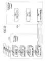
- FIG. 3shows a digital camera 200 configured for simultaneous acquisition of multiple fields of view, under an embodiment.
- the digital camera 200includes a digital camera subsystem 210 , an electronic image storage media 220 , a power supply 224 , a peripheral user interface (represented as a shutter button) 232 , a circuit board 236 that supports and/or electrically couples or interconnects the components, a housing 240 (including housing portions 241 , 242 , 243 , 244 , 245 and 246 ) and a shutter assembly (not shown), which controls an aperture 250 and passage of light into the digital camera 200 .
- a housing 240including housing portions 241 , 242 , 243 , 244 , 245 and 246
- a shutter assemblynot shown
- the digital camera subsystem (DCS) 210includes one or more camera channels (e.g., four camera channels 260 A- 260 D) and replaces and/or fulfills one, some or all of the roles fulfilled by the lens assembly 110 , the color filter 112 and the image sensor 116 of the digital camera 100 described above.
- the four camera channels 260 A- 260 Dare configured through pixel array size and/or optical focal length to provide a desired field of view for that channel.
- the four camera channels 260 A- 260 Dcan be operated simultaneously with independent electrical control of features such as integration time control and frame rate (in video applications) to name a few.
- the peripheral user interface 232which includes the shutter button, can include one or more additional input devices (e.g., for settings, controls and/or input of other information).
- the peripheral user interface 232can also include one or more output devices, (e.g., a display for output of images or other information) and associated electronics.
- the electronic image storage media 220 , power supply 224 , peripheral user interface 232 , circuit board 236 , housing 240 , shutter assembly (not shown), and aperture 250may be, for example, similar to the electronic image storage media 120 , power supply 124 , peripheral user interface 132 , circuit board 136 , housing 140 , shutter assembly (not shown), and aperture 150 of the digital camera 100 described above.
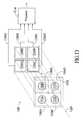
- FIG. 4is a digital camera system 210 that includes multiple camera channels, under an embodiment.
- the digital camera system 210 of this exampleincludes four camera channels 260 A- 260 D but is not limited to four camera channels; alternative embodiments can have any number of camera channels.
- Each of the camera channels 260 A- 260 Dincludes an optics component or portion and a sensor component or portion.
- camera channel 260 Aincludes an optics portion 290 A and a sensor portion 292 A.
- Camera channel Bincludes an optics portion 290 B and a sensor portion 292 B.
- Camera channel Cincludes an optics portion 290 C and a sensor portion 292 C.
- Camera channel Dincludes an optics portion 290 D and a sensor portion 292 D.
- the optics portions of the one or more camera channelsare collectively referred to herein as an optics subsystem.
- the sensor portions of the one or more camera channelsare collectively referred to herein as a sensor subsystem.
- Each camera channel of the digital camera subsystem 210 of an embodimentprovides a different FOV imaging capability relative to at least one other camera channel.
- one camera channele.g. camera channel 260 A
- one camera channele.g., camera channel 260 B
- detects a medium field of viewe.g. 20° ⁇ 15°
- one camera channele.g., camera channel 260 C
- detects a narrow field of viewe.g. 12° ⁇ 9°
- one camera channele.g., camera channel 260 D
- detects light in a very narrow field on viewe.g. 5° ⁇ 5°.
- the digital camera subsystems of one or more alternative embodimentsmay configure one or more of the camera channels to have different fields of view than those described above.
- one camera channele.g. camera channel 260 A
- one camera channele.g., camera channel 260 B
- detects a medium field of viewe.g. 30° ⁇ 15°
- one camera channele.g., camera channel 260 C
- detects a narrow field of viewe.g. 12° ⁇ 9°
- one camera channele.g., camera channel 260 D
- detects light in a very narrow field on viewe.g. 5° ⁇ 5°.
- one camera channele.g. camera channel 260 A
- two camera channelse.g., camera channel 260 B and 260 C
- medium field of viewe.g. 20° ⁇ 15°
- one camera channele.g., camera channel 260 D
- a narrow field of viewe.g. 12° ⁇ 9°
- the FOV(also referred to as angle of view) describes the angular extent of a given scene that is imaged by a camera.
- the FOV of a camerais a function of parameters that include the focal length of the photographic lens projecting the image and the dimensions of the image sensor. Therefore, the digital cameras of an embodiment can provide a different FOV in each channel by controlling or varying parameters of the focal length of the photographic lens in combination with parameters of the image sensor.
- the sensor dimensionscan be approximately the same for the sensors of all channels of the camera while the focal length of the optics component varies among the channels.
- the focal length of the optics componentscan be approximately the same in all channels while the sensor dimensions vary among the channels.
- the focal length of the optics component and the sensor dimensionsboth vary among the channels.
- the optics portion of each camera channelcan be configured similar to and/or different from the optics portion of at least one other camera channel.
- embodiments of the digital camera subsystem 210include optics portions that are configured approximately the same while having a different sensor array size (area) between camera channels to provide a different FOV capability.
- the sensor array area changecan be accomplished by changing the number of pixels and/or pixel size of the array.
- parameters of the image sensor electrical operatione.g., integration time, frame rate, etc.
- the optics portion of one or more camera channelsis configured differently, in one or more respects (e.g., focal length, f-number, etc.), from the optics portion of one or more other camera channels.
- at least one characteristice.g., type of element(s), size, performance, etc.
- the optics portionsis configured to the respective sensor portion and/or to achieve a desired result.
- the optics portion for that camera channelmay be configured to transmit only that particular color (or band of colors) or wavelength (or band of wavelengths) to the sensor portion of the particular camera channel.
- the optics portion for that camera channelmay be configured to filter out one or more other colors or wavelengths.
- the sensor portion of each camera channel of the digital camera subsystem 210can be configured similar to and/or different from the sensor portion of at least one other camera channel.
- the sensor portions of each camera channelare similarly configured.
- a configuration of one or more of sensor portionsis different, in one or more respects, from one or more of the other sensor portions.
- one or more of the characteristics (e.g., type of element(s), size, performance, etc.) of one or more of the sensor portionsis configured to the respective optics portion and/or to help achieve a desired result.
- the sensor portion for that camera channelmay be configured to have a sensitivity that is higher to that particular color (or band of colors) or wavelength (or band of wavelengths) than other colors or wavelengths and/or to sense only that particular color (or band of colors) or wavelength (or band of wavelengths).
- the sensor portion for other camera channelsmay be configured to have a relatively low sensitivity to that particular color (or band of colors) or wavelength (or band of wavelengths) and/or to not detect that particular color (or band of colors) or wavelength (or band of wavelengths).
- the digital camera system 210 of an embodimentincludes a processor.
- the processorincludes an image processor component or circuitry (referred to herein as image processor 270 ) and a controller component or circuitry (referred to herein as controller 300 ).
- the controller 300is part of a positioning system 280 .
- the processor 270is coupled or connected to the one or more sensor portions (e.g. sensor portions 292 A- 292 D) via one or more communication links, represented by a signal line 330 .
- the positioning system 280includes the controller 300 and one or more positioners (e.g., positioners 310 and 320 ).
- the controller 300is coupled or connected to the image processor 270 via one or more communication links 340 .
- the controller 300is coupled or connected to one or more of the positioners (e.g., positioners 310 and 320 ) via one or more communication links (e.g. some number of electrical signal lines) 350 and 360 .
- the positionersare adapted to support and/or position each of the one or more optics portions (e.g., optics portions 290 A- 290 D) of a camera channel above and/or in registration with the sensor portions (e.g., sensor portions 292 A- 292 D 0 of the respective camera channels.
- the positioner 310supports and positions the one or more optics portions (e.g. optics portions 290 A- 290 D) at least in part.
- the positioner 320supports and positions the one or more sensor portions (e.g. sensor portions 292 A- 292 D) at least in part.
- One or more of the positioners 310 and 320can also be configured to provide or help provide relative movement between one or more of the respective optics portions 290 A- 290 D and one or more of the respective sensor portions 292 A- 292 D.
- Aspects of the positioning system 280are described in detail in U.S. patent application Ser. No. 11/478,242, filed Jun. 29, 2006, which application claims the benefit of U.S. Patent Application No. 60/695,946, filed Jul. 1, 2005, both of which are herein incorporated by reference.
- an optics portion of a first camera channelreceives light from within a first field of view and transmits one or more portions of the received light to the corresponding sensor portion.
- the sensor portion of the first camera channelreceives one or more portions of the light transmitted by the optics portion and outputs a signal representative of the received light.
- the output signal from the sensor portionis coupled to the image processor, which can generate an image or data based at least in part on information of the output signal.
- An optics portion of a second camera channelreceives light from within a second field of view and transmits one or more portions of the received light to the corresponding sensor portion.
- the sensor portion of the second camera channelreceives one or more portions of the light transmitted by the optics portion and outputs a signal representative of the received light.
- the output signal from the sensor portionis coupled to the image processor, which can generate an image or data based at least in part on information of the output signal.
- the operations of the second camera channelare simultaneous or nearly simultaneous with the operations of the first camera channel. Operations of any additional camera channels are similar to operations of the first and/or second camera channels described above.
- the image processoris configured to generate or composite an image based on data from one or more of the camera channels.
- the image processor of an embodimentis configured to generate a combined image or data based at least in part on the images from the first and second camera channels (and additional camera channels when present), or to independently output camera channel data of each camera channel.
- the positioning systemcan control movement of the optics portion (or portions thereof) and/or the sensor portion (or portions thereof) of each camera channel to provide relative positioning with respect to one or operating modes of the digital camera system.
- FIG. 5is a flow diagram for simultaneous acquisition of multiple fields of view 500 , under an embodiment.
- the simultaneous acquisition of images having multiple fields of view 500includes configuring 502 a first camera channel to have a first optical focal length.
- the acquisition 500includes configuring 504 a second camera channel to have a second optical focal length that is different from the first optical focal length.
- An imageis captured 506 by the first camera channel, and the image of the first camera channel has a first field of view.
- the imageis captured 508 by the second camera channel.
- the image captured by the second camera channelhas a second field of view that is different from the first field of view.
- additional camera channelscapture the image with the first field of view, the second field of view, or a field of view different from the first and second field of view.
- FIGS. 6-19illustrate further examples of apparatus and systems in which the imaging module and focusing method embodiments disclosed above can be implemented.
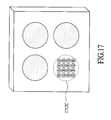
- FIG. 6is a block diagram of a digital camera 600 , under an embodiment.
- the digital cameraincludes a digital camera subsystem 602 , a circuit board 612 , a peripheral user interface electronics 610 (here represented as a shutter button, but could also include display and/or one or more other output devices, setting controls and/or one or more additional input devices etc), a power supply 606 , and electronic image storage media 604 .
- the digital camera 600may further include a housing and a shutter assembly (not shown), which controls an aperture 614 and passage of light into the digital camera 600 .
- FIG. 7is an exploded view of the digital camera subsystem 602 , under an embodiment.
- the digital camera subsystemincludes an image sensor 704 , an optics frame (also referred to as a frame) 702 , and lenses 712 A- 712 D.
- the frame 702is used to mount the lenses 712 A- 712 D to the image sensor 704 .
- the image sensor, or imager die 704generally includes a semiconductor integrated circuit or “chip” having several higher order features including multiple arrays 704 A- 704 D and signal processing circuits 708 and 710 . Each of the arrays 704 A- 704 D captures photons and outputs electronic signals.
- the signal processing circuit 708processes signals for each of the individual arrays 704 .
- the signal processing circuit 710may combine the output from signal processing 708 into output data (usually in the form of a recombined full color image). Each array and the related signal processing circuitry may be tailored to address a specific band of visible spectrum.
- Each of lenses 712 A- 712 Dmay be tailored for the respective wavelength of the respective array.
- Lensesare approximately the same size as the underlying array 704 , and will differ from one another in size and shape depending upon the dimensions of the underlying array. In alternative embodiments a lens could cover only a portion of an array, and could extend beyond the array.
- Lensescan comprise any suitable material or materials, including for example, glass and plastic. Lenses can be doped in any suitable manner, such as to impart a color filtering, polarization, or other property. Lenses can be rigid or flexible.
- each lens, array, and signal processing circuitconstitutes an image generating subsystem for a band of visible spectrum (e.g., red, blue, green, etc). These individual images are then combined with additional signal processing circuitry within the semiconductor chip to form a full image for output.
- a band of visible spectrume.g., red, blue, green, etc.
- FIG. 8is a block diagram of a digital camera 800 having a three array/lens configuration, under an embodiment.
- the digital camera 800includes a digital camera subsystem 802 that includes three lenses.
- the digital camera 800further includes a circuit board 812 , a peripheral user interface electronics 810 (here represented as a shutter button, but could also include display and/or one or more other output devices, setting controls and/or one or more additional input devices etc), a power supply 806 , and electronic image storage media 804 .
- the digital camera 800may further include a housing and a shutter assembly (not shown), which controls an aperture 814 and passage of light into the digital camera 800 .
- FIG. 9is a block diagram of a digital camera subsystem that employs separate arrays, e.g., arrays 904 A- 904 D, on one image sensor, in contrast to the prior art.
- arrays 904 A- 904 De.g., arrays 904 A- 904 D
- typical prior art approachesemploy a Bayer pattern (or variations thereof), perform operations across the array (a pixel at a time), and integrate each set of four pixels (for example, red/green/blue/green or variation thereof) from the array into a single full color pixel.
- Each of the arrays 904focuses on a specific band of visible spectrum. Each lens only needs to pass a respective color ( 906 A- 906 D) on to the image sensor. The traditional color filter sheet is eliminated.
- Each array 904outputs signals to signal processing circuitry. Signal processing circuitry for each of these arrays is also tailored for each of the bands of visible spectrum. In effect, individual images are created for each of these arrays. Following this process, the individual images are combined or to form one full color or black/white image. By tailoring each array and the associated signal processing circuitry, a higher quality image can be generated than the image resulting from traditional image sensors of like pixel count.
- each arraymay be tuned to be more efficient in capturing and processing the image in that particular color.
- Individual lenses ( 912 A-D)can be tailored for the array's band of spectrum.
- FIG. 10is a block diagram of arrays 1004 A- 1004 D.
- Each array 1004receives a respective color as passed by a respective lens. The traditional color filter sheet is eliminated.
- Each array 1004outputs signals to signal processing circuitry.
- Signal processing circuitry for each of these arraysis also tailored for each of the bands of visible spectrum. In effect, individual images are created for each of these arrays. Following this process, the individual images are combined or to form one full color or black/white image. By tailoring each array and the associated signal processing circuitry, a higher quality image can be generated than the image resulting from traditional image sensors of like pixel count.
- FIG. 11is a block diagram of processing circuitry of a digital camera subsystem, under an embodiment.
- FIG. 11includes an array 1104 , including arrays 1104 A- 1104 D, and signal processing circuitry (also referred to as image processing circuitry) 1214 and 1216 . Each array outputs signals to signal processing circuitry.
- FIG. 12is a block diagram of image processing circuitry 1214 and 1216 .
- each arraycan be processed separately to tailor the processing to the respective bands of spectrum.
- Column logic 1214 . 1 A- 1214 . 1 Dis the portion of the signal processing circuitry that reads the signals from the pixels.
- the column logic 1214 . 1 Areads signals from the pixels in array 1204 A.
- Column logic 1214 . 1 Breads signals from the pixels in array 1204 B.
- Column logic 1214 . 1 Creads signals from the pixels in array 1204 C.
- Column logic 1214 . 1 Dreads signals from the pixels in array 1204 D.
- the column logicmay have different integration times for each array enhancing dynamic range and/or color specificity. Signal processing circuitry complexity for each array can be substantially reduced since logic may not have to switch between extreme color shifts.
- Analog Signal Logic (ASL) 1214 . 2 A- 1214 . 2 D for each arraymay be color specific. As such, the ASL processes a single color and therefore can be optimized for gain, noise, dynamic range, linearity, etc. Due to color signal separation, dramatic shifts in the logic and settling time are not required as the amplifiers and logic do not change on a pixel by pixel (color to color) basis as in traditional Bayer patterned designs.
- ASLAnalog Signal Logic
- Black level control 1214 . 3 A- 1214 . 3 Dassesses the level of noise within the signal, and filters it out. With each array focused upon a narrower band of visible spectrum than traditional image sensors, the black level control can be more finely tuned to eliminate noise.
- Exposure control 1214 . 4 A- 1214 . 4 Dmeasures the overall volume of light being captured by the array and adjusts the capture time for image quality. Traditional cameras must make this determination on a global basis (for all colors). The embodiments describe herein allow for exposure control to occur differently for each array and targeted band of wavelengths.
- image processing logic 1216 . 1integrates the multiple color planes into a single color image. The image is adjusted for saturation, sharpness, intensity, hue, artifact removal, and defective pixel correction.
- the final two operationsinclude encoding the signal into standard protocols such as MPEG, JPEG, etc. in an encoder 1216 . 2 before passing the result to a standard output interface 1216 . 3 , such as USB.
- standard protocolssuch as MPEG, JPEG, etc.
- the signal processing circuitries 1214 and 1216are shown at specific areas of the image sensor, the signal processing circuitries 1214 and 1216 can be placed anywhere on the chip and subdivided in any fashion. The signal processing circuitries are often placed in multiple locations.
- the image sensor 1204generally includes a semiconductor chip having several higher order features including multiple arrays ( 1204 A- 1204 D), and signal processing circuitry 1214 , in which each array and the related signal processing circuitry is preferably tailored to address a specific band of visible spectrum.
- the image sensor arraycan be configured using any multiple numbers and shapes of arrays.
- the image sensor 1204can be constructed using any suitable technology, including silicon and germanium technologies.
- the pixelscan be formed in any suitable manner, can be sized and dimensioned as desired, and can be distributed in any desired pattern. Pixels that are distributed without any regular pattern may also be used.
- any range of visible spectrumcan be applied to each array depending on the specific interest of the customer. Further, an infrared array could also be employed as one of the array/lens combinations giving low light capabilities to the sensor.
- arrays 1204 A- 1204 Dmay be of any size or shape. While some figures referenced herein show the arrays as individual, discrete sections of the image sensor, these arrays may also be touching. There may also be one large array configured such that the array is subdivided into sections, and each section is focused upon one band of spectrum, creating the same effect as separate arrays on the same chip.
- a photo detectorincludes an area or portion of the photo detector that captures, collects, is responsive to, detects and/or senses the intensity illumination of incident light.
- the well depthis the distance from the surface of the photo detector to a doped region.
- Selection of an appropriate well depthdepends on many factors, including the targeted band of visible spectrum. Since each entire array is likely to be targeted at one band of visible spectrum (e.g., red) the well depth can be configured to capture that wavelength and ignore others (e.g., blue, green). Doping of the semiconductor material in the color specific arrays can further be used to enhance the selectivity of the photon absorption for color-specific wavelengths.
- a digital camera subsystemcan have multiple separate arrays on a single image sensor, each with its own lens.
- the simple geometry of smaller, multiple arraysallows for a smaller lenses (e.g., smaller diameter, thickness and focal length), which allows for reduced stack height in the digital camera.
- the lens and frame conceptis applicable to traditional image sensors (without the traditional color filter sheet) to gain physical size, cost and performance advantages.
- Each arraycan advantageously be focused on one band of visible and/or detectable spectrum.
- each lensmay be tuned for passage of one specific band of wavelength. Since each lens would therefore not need to pass the entire light spectrum, the number of elements may be reduced, for example, to one or two.
- each of the lensesmay be dyed during the manufacturing process for its respective bandwidth (e.g., red for the array targeting the red band of visible spectrum).
- a single color filtermay be applied across each lens. This process eliminates the traditional color filters (such as the sheet of individual pixel filters) thereby reducing cost, improving signal strength and eliminating the pixel reduction barrier.
- the above-described devicescan include any suitable number of combinations, including as few as two arrays/lenses, and many more than two arrays/lenses. Examples include: two arrays/lenses configured as red/green and blue; two arrays/lenses configured as red and blue/green; two arrays/lenses configured as red, green, blue; four arrays/lenses configured as red, blue, green, emerald (for color enhancement); four arrays/lenses configured as red, blue, green, infrared (for low light conditions); and eight arrays/lenses configured as double the above configurations for additional pixel count and image quality.
- the cameras or camera subsystems described hereinare intended to be emblematic of a generic appliance containing the digital camera subsystem.
- the description hereinshould be interpreted as being emblematic of still and video cameras, cell phones, other personal communications devices, surveillance equipment, automotive applications, computers, manufacturing and inspection devices, toys, plus a wide range of other and continuously expanding applications.
- these alternative interpretationsmay or may not include the specific components as depicted herein.
- the circuit boardmay not be unique to the camera function but rather the digital camera subsystem may be an add-on to an existing circuit board, such as in a cell phone.
- any or all of the methods and/or apparatus disclosed hereinmay be employed in any type of apparatus or process including, but not limited to still and video cameras, cell phones, other personal communications devices, surveillance equipment, automotive applications, computers, manufacturing and inspection devices, toys, plus a wide range of other and continuously expanding applications.
- each array and the related signal processing circuitryis can be tailored to address a specific band of visible spectrum, and each lens may be tuned for passage of that one specific band of wavelength, there is no requirement that each such array and the related signal processing circuitry be tailored to address a specific band of the visible spectrum. Nor is there any requirement that each lens be tuned for passage of a specific band of wavelength or that each of the arrays be located on the same semiconductor device. Indeed, the embodiments described and illustrated herein, including the specific components thereof, need not employ wavelength-specific features. For example, the arrays and/or signal processing circuitry need not be tailored to address a specific wavelength or band of wavelengths.
- FIG. 13is an exploded perspective view of a digital camera 1300 , under an embodiment.
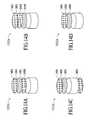
- the digital camera apparatus 1300includes one or more sensor arrays, e.g., four sensor arrays 1304 A- 1304 D, and one or more optics portions, e.g., four optics portions 1312 A- 1312 D.
- Each of the optics portions 1304 A- 1304 Dmay include a lens, and may be associated with a respective one of the sensor arrays sensor arrays 1304 A- 1304 D.
- a support 1302for example a frame, is provided to support the one or more optics portions 1312 A- 1312 D, at least in part.
- Each sensor array and the respective optics portionmay define an optical channel.
- an optical channel 1306 Amay be defined by the optics portion 1312 A and the sensor array 1304 A.
- An optical channel 1306 Bmay be defined by the optics portion 1312 B and the sensor array 1304 B.
- An optical channel 1306 Cmay be defined by optics portion 1312 C and the sensor array 1304 C.
- An optical channel 1306 Dmay be defined by optics portion 1312 D and a sensor array 1304 D.
- the optics portions of the one or more optical channelsare also collectively referred to as an optics subsystem.
- the sensor arrays of the one or more optical channelsare collectively referred as a sensor subsystem.
- the two or more sensor arraysmay be integrated in or disposed on a common substrate, referred to as an image device, on separate substrates, or any combination thereof.
- the systemincludes three or more sensor arrays, two or more sensor arrays may be integrated in a first substrate, and one or more other sensor arrays may be integrated in or disposed on a second substrate.
- the one or more sensor arrays 1304 A- 1304 Dmay or may not be disposed on a common substrate.
- two or more of the sensor arraysare disposed on a common substrate.
- one or more of the sensor arraysis not disposed on the same substrate as one or more of the other sensor arrays.
- the one or more optical channelsmay or may not be identical to one another.
- one of the optical channels 1306detects red light, one of the optical channels 1306 detects green light, and one of the optical channels 1306 detects blue light. In some of such embodiments, one of the optical channels 1306 detects infrared light, cyan light, or emerald light. In some other embodiments, one of the optical channels 1306 detects cyan light, one of the optical channels 1306 detects yellow light, one of the optical channels 1306 detects magenta light and one of the optical channels 1306 detects clear light (black and white). Any other wavelength or band of wavelengths (whether visible or invisible) combinations can also be used.
- a processor 1314is coupled to the one or more sensor arrays 1304 A- 1304 D, via one or more communication links, e.g., communication links 1308 A- 1308 D, respectively.
- a communication linkmay be any kind of communication link including but not limited to, for example, wired (e.g., conductors, fiber optic cables) or wireless (e.g., acoustic links, electromagnetic links or any combination thereof including but not limited to microwave links, satellite links, infrared links), and combinations thereof, each of which may be public or private, dedicated and/or shared (e.g., a network).
- a communication linkmay include for example circuit switching or packet switching or combinations thereof. Other examples of communication links include dedicated point-to-point systems, wired networks, and cellular telephone systems.
- a communication linkmay employ any protocol or combination of protocols including but not limited to the Internet Protocol.
- the communication linkmay transmit any type of information.
- the informationmay have any form, including, for example, but not limited to, analog and/or digital) e.g., a sequence of binary values, or a bit string).
- the informationmay or may not be divided into blocks. If divided into blocks, the amount of information in a block may be predetermined or determined dynamically, and/or may be fixed (e.g., uniform) or variable.
- the processormay include one or more channel processors, each of which is coupled to a respective one (or more) of the optical channels and generates an image based at least in part on the signal(s) received from the respective optical channel, although this is not required.
- one or more of the channel processorsis tailored to its respective optical channel, for example, as described herein. For example, when one of the optical channels is dedicated to a specific wavelength or color (or band of wavelengths or colors) the respective channel processor may be adapted or tailored to such wavelength or color (or band of wavelengths or colors).
- the gain, noise reduction, dynamic range, linearity and/or any other characteristic of the processor, or combinations of such characteristicsmay be adapted to improve and/or optimize the processor to such wavelength or color (or band of wavelengths or colors). Tailoring the channel processing to the respective optical channel may facilitate generating an image of a quality that is higher than the quality of images resulting from traditional image sensors of like pixel count.
- providing each optical channel with a dedicated channel processormay help to reduce or simplify the amount of logic in the channel processors as the channel processor may not need to accommodate extreme shifts in color or wavelength, e.g., from a color (or band of colors) or wavelength (or band of wavelengths) at one extreme to a color (or band of colors) or wavelength (or band of wavelengths) at another extreme.
- an optics portion of a optical channelreceives light from within a field of view and transmits one or more portions of such light, e.g., in the form of an image at an image plane.
- the sensor arrayreceives one or more portions of the light transmitted by the optics portion and provides one or more output signals indicative thereof.
- the one or more output signals from the sensor arrayare supplied to the processor.
- the processorgenerates one or more output signals based, at least in part, on the one or more signals from the sensor array.
- the processormay generate a combined image based, at least in part, on the images from two or more of such optical channels.
- the processor 1314may have any configuration and may be disposed in one or more locations. For example, certain operations of the processor may be distributed to or performed by circuitry that is integrated in or disposed on the same substrate or substrates as one or more of the one or more of the sensor arrays and certain operations of the processor are distributed to or performed by circuitry that is integrated in or disposed on one or more substrates that are different from (whether such one or more different substrates are physically located within the camera or not) the substrates the one or more of the sensor arrays are integrated in or disposed on.
- the digital camera apparatus 1300may or may not include a shutter, a flash and/or a frame to hold the components together.
- FIGS. 14A-14Dare schematic exploded representations of one embodiment of an optics portion, such as optic portion 1312 A, under an embodiment.
- the optics portion 1312 Aincludes one or more lenses, e.g., a complex aspherical lens module 1480 , one or more color coatings, e.g., a color coating 1482 , one or more masks, e.g., an auto focus mask 1484 , and one or more IR coatings, e.g., an IR coating 1486 .
- Lensescan comprise any suitable material or materials, including for example, glass and plastic. Lenses can be doped in any suitable manner, such as to impart a color filtering, polarization, or other property. Lenses can be rigid or flexible. In this regard, some embodiments employ a lens (or lenses) having a dye coating, a dye diffused in an optical medium (e.g., a lens or lenses), a substantially uniform color filter and/or any other filtering technique through which light passes to the underlying array.
- an optical mediume.g., a lens or lenses
- the color coating 1482helps the optics portion filter (or substantially attenuate) one or more wavelengths or bands of wavelengths.
- the auto focus mask 1484may define one or more interference patterns that help the digital camera apparatus perform one or more auto focus functions.
- the IR coating 1486helps the optics portion 1312 A filter a wavelength or band of wavelength in the IR portion of the spectrum.
- the one or more color coatingse.g., color coating 1482 , one or more masks, e.g., mask 1484 , and one or more IR coatings, e.g., IR coating 1486 may have any size, shape and/or configuration.
- one or more of the one or more color coatingsare disposed at the top of the optics portion.
- Some embodiments of the optics portionmay or may not include the one or more color coatings, one or more masks and one or more IR coatings and may or may not include features in addition thereto or in place thereof.
- one or more of the one or more color coatingsare replaced by one or more filters 1488 disposed in the optics portion, e.g., disposed below the lens.
- one or more of the color coatingsare replaced by one or more dyes diffused in the lens.
- the one or more optics portionsmay or may not be identical to one another.
- the optics portionsare identical to one another.
- one or more of the optics portionsare different, in one or more respects, from one or more of the other optics portions.
- one or more of the characteristicsfor example, but not limited to, its type of element(s), size, response, and/or performance
- the characteristicsfor example, but not limited to, its type of element(s), size, response, and/or performance
- the optics portion for that optical channelmay be adapted to transmit only that particular color (or band of colors) or wavelength (or band of wavelengths) to the sensor array of the particular optical channel and/or to filter out one or more other colors or wavelengths.
- the design of an optical portionis optimized for the respective wavelength or bands of wavelengths to which the respective optical channel is dedicated. It should be understood, however, that any other configurations may also be employed.
- Each of the one or more optics portionsmay have any configuration.
- each of the optics portionscomprises a single lens element or a stack of lens elements (or lenslets), although, as stated above.
- a single lens element, multiple lens elements and/or compound lenses, with or without one or more filters, prisms and/or masksare employed.
- An optical portioncan also contain other optical features that are desired for digital camera functionality and/or performance.
- these featurescan include electronically tunable filters, polarizers, wavefront coding, spatial filters (masks), and other features not yet anticipated.
- Some of the featuresare electrically operated (such as a tunable filter), or are mechanically movable with MEMs mechanisms.
- one or more photochromic (or photochromatic) materialsare employed in one or more of the optical portions.
- the one or more materialsmay be incorporated into an optical lens element or as another feature in the optical path, for example, above one or more of the sensor arrays.
- photochromatic materialsmay be incorporated into a cover glass at the camera entrance (common aperture) to all optics (common to all optical channels), or put into the lenses of one or more optical channels, or into one or more of the other optical features included into the optical path of an optics portion over any sensor array.
- FIGS. 15A-15Care schematic representations of one embodiment of a sensor array 1504 .
- the sensor arrayis similar to one of the sensor arrays 1304 A- 1304 D of FIG. 13 , foe example.
- the sensor array 1504is coupled to circuits 1570 , 1572 , and 1574 .
- the sensor array sensor array 1504captures light and converts it into one or more signals, such as electrical signals, which are supplied to one or more of the circuits 1570 , 1572 , and 1574 .
- the sensor array 1504includes a plurality of sensor elements such as for example, a plurality of identical photo detectors (sometimes referred to as “picture elements” or “pixels”), e.g., pixels 1580 1,1 - 1580 n,m .
- the photo detectors 1580 1,1 - 1580 n,mare arranged in an array, for example a matrix-type array.
- the number of pixels in the arraymay be, for example, in a range from hundreds of thousands to millions.
- the pixelsmay be arranged for example, in a two-dimensional array configuration, for example, having a plurality of rows and a plurality of columns, e.g., 640 ⁇ 480, 1280 ⁇ 1024, etc.
- a pixelfor example pixel 1580 1,1
- a pixelmay be viewed as having x and y dimensions, although the photon capturing portion of a pixel may or may not occupy the entire area of the pixel and may or may not have a regular shape.
- the sensor elementsare disposed in a plane, referred to herein as a sensor plane.
- the sensormay have orthogonal sensor reference axes, including for example, an x-axis, a y-axis, and a z-axis, and may be configured so as to have the sensor plane parallel to the x-y plane XY and directed toward the optics portion of the optical channel.
- Each optical channelhas a field of view corresponding to an expanse viewable by the sensor array.
- Each of the sensor elementsmay be associated with a respective portion of the field of view.
- the sensor arraymay employ any type of technology, for example, but not limited to MOS pixel technologies (e.g., one or more portions of the sensor are implemented in “Metal Oxide Semiconductor” technology), charge coupled device (CCD) pixel technologies, or combination of both.
- MOS pixel technologiese.g., one or more portions of the sensor are implemented in “Metal Oxide Semiconductor” technology
- CCDcharge coupled device
- the sensor arraymay comprise any suitable material or materials, including, but not limited to, silicon, germanium and/or combinations thereof.
- the sensor elements or pixelsmay be formed in any suitable manner.
- the sensor array 1504 Ais exposed to light on a sequential line per line basis (similar to a scanner, for example) or globally (similar to conventional film camera exposure, for example). After being exposed to light for certain period of time (exposure time), the pixels 1580 1,1 - 1580 n,m , are read out, e.g., on a sequential line per line basis.
- circuitry 1570is used to read the signals from the pixels 1580 1,1 - 1580 n,m .
- FIG. 15Cis a schematic representation of a pixel circuit.
- the pixels 1580 1,1 - 1580 nalso referred to as sensor elements, may be accessed one row at a time by asserting one of the word lines 1582 , which run horizontally through the sensor array 1504 A.
- a single pixel 1580 1,1is shown.
- Datais passed into and/or out of the pixel 1580 1,1 via bit lines (such as bit line 1584 ) which run vertically through the sensor array 1504 A.
- each of the one or more sensor arraysmay have any configuration (e.g., size, shape, pixel design).
- the sensor arrays 1302 A- 1302 D of FIG. 13may or may not be identical to one another. In some embodiments, for example, the sensor arrays are identical to one another. In some other embodiments, one or more of the sensor arrays are different, in one or more respects, from one or more of the other sensor arrays. For example, in some embodiments, one or more of the characteristics (for example, but not limited to, its type of element(s), size (for example, surface area), and/or performance) of one or more of the sensor arrays is tailored to the respective optics portion and/or to help achieve a desired result.
- the characteristicsfor example, but not limited to, its type of element(s), size (for example, surface area), and/or performance
- FIG. 16is a schematic cross-sectional view of a digital camera apparatus 1600 including a printed circuit board 1620 of a digital camera on which the digital camera elements are mounted, under an embodiment.
- the one or more optics portionse.g., optics portions 1612 A and 1612 B are seated in and/or affixed to a support 1614 .
- the support 1614(for example a frame) is disposed superjacent a first bond layer 1622 , which is disposed superjacent an image device 1620 , in or on which sensor portions 1612 A- 1612 D (sensor portions 1612 C and 1612 D are not shown), are disposed and/or integrated.
- the image device 1620is disposed superjacent a second bond layer 1624 which is disposed superjacent the printed circuit board 1621 .
- the printed circuit board 1621includes a major outer surface 1630 that defines a mounting region on which the image device 1620 is mounted.
- the major outer surface 1630may further define and one or more additional mounting regions (not shown) on which one or more additional devices used in the digital camera may be mounted.
- One or more pads 1632are provided on the major outer surface 1630 of the printed circuit board to connect to one or more of the devices mounted thereon.
- the image device 1620includes the one or more sensor arrays (not shown), and one or more electrically conductive layers. In some embodiments, the image device 1620 further includes one, some or all portions of a processor for the digital camera apparatus 1600 . The image device 1620 further includes a major outer surface 1640 that defines a mounting region on which the support 1614 is mounted.
- the one or more electrically conductive layersmay be patterned to define one or more pads 1642 and one or more traces (not shown) that connect the one or more pads to one or more of the one or more sensor arrays.
- the pads 1642are disposed, for example, in the vicinity of the perimeter of the image device 1620 , for example along one, two, three or four sides of the image device 1620 .
- the one or more conductive layersmay comprise, for example, copper, copper foil, and/or any other suitably conductive material(s).
- a plurality of electrical conductors 1650may connect one or more of the pads 1642 on the image device 1620 to one or more of the pads 1632 on the circuit board 1621 .
- the conductors 1650may be used, for example, to connect one or more circuits on the image device 1620 to one or more circuits on the printed circuit board 1621 .
- the first and second bond layers 1622 and 1624may comprise any suitable material(s), including but not limited to adhesive, and may comprise any suitable configuration.
- the first and second bond layers 1622 , 1624may comprise the same material(s) although this is not required.
- a bond layermay be continuous or discontinuous.
- a conductive layermay be an etched printed circuit layer.
- a bond layermay or may not be planar or even substantially planar.
- a conformal bond layer on a non-planar surfacewill be non-planar.
- FIG. 17is a schematic perspective view of a digital camera apparatus having one or more optics portions with the capability to provide color separation in accordance with one embodiment of the present invention.
- one or more of the optics portions, e.g., optics portion 1712 Cincludes an array of color filters, for example, but not limited to a Bayer patter.
- one or more of the optics portions, e.g., optics portion 1712 Chas the capability to provide color separation similar to that which is provided by a color filter array.
- the lens and/or filter of the optical channelmay transmit both of such colors or bands of colors, and the optical channel may include one or more mechanisms elsewhere in the optical channel to separate the two colors or two bands of colors.
- a color filter arraymay be disposed between the lens and the sensor array, and/or the optical channel may employ a sensor capable of separating the colors or bands of colors.
- the sensor arraymay be provided with pixels that have multiband capability, e.g., two or three colors.
- each pixelmay comprise two or three photodiodes, wherein a first photodiode is adapted to detect a first color or first band of colors, a second photodiode is adapted to detect a second color or band of colors and a third photodiode is adapted to detect a third color or band of colors.
- One way to accomplish thisis to provide the photodiodes with different structures and/or characteristics that make them selective, such that the first photodiode has a higher sensitivity to the first color or first band of colors than to the second color or band of colors, and the second photodiode has a higher sensitivity to the second color or second band of colors than to the first color or first band of colors.
- the photodiodesare disposed at different depths in the pixel, taking advantage of the different penetration and absorption characteristics of the different colors or bands of colors. For example, blue and blue bands of colors penetrate less (and are thus absorbed at a lesser depth) than green and green bands of colors, which in turn penetrate less (and are thus absorbed at a lesser depth) than red and red bands of colors.
- such a sensor arrayis employed, even though the pixels may see only one particular color or band of colors, for example, to in order to adapt such sensor array to the particular color or band of colors.
- FIG. 18Ais a block diagram of a processor 1802 of a digital camera subsystem 1800 , under an embodiment.
- the processor 1802includes one or more channel processors, one or more image pipelines, and/or one or more image post processors.
- Each of the channel processorsis coupled to a respective one of the optical channels (not shown) and generates an image based at least in part on the signal(s) received from the respective optical channel.
- the processor 1802generates a combined imaged based at least in part on the images from two or more of the optical channels.
- one or more of the channel processorsare tailored to its respective optical channel, as previously described.
- the gain, noise reduction, dynamic range, linearity and/or any other characteristic of the processor, or combinations of such characteristicsmay be adapted to improve and/or optimize the processor to a wavelength or color (or band of wavelengths or colors). Tailoring the channel processing to the respective optical channel makes it possible to generate an image of a quality that is higher than the quality of images resulting from traditional image sensors of like pixel count.
- providing each optical channel with a dedicated channel processorhelps to reduce or simplify the amount of logic in the channel processors, as the channel processor may not need to accommodate extreme shifts in color or wavelength, e.g., from a color (or band of colors) or wavelength (or band of wavelengths) at one extreme to a color (or band of colors) or wavelength (or band of wavelengths) at another extreme
- the images (and/or data which is representative thereof) generated by the channel processorsare supplied to the image pipeline, which may combine the images to form a full color or black/white image.
- the output of the image pipelineis supplied to the post processor, which generates output data in accordance with one or more output formats.
- FIG. 18Bshows one embodiment of a channel processor.
- the channel processorincludes column logic, analog signal logic, and black level control and exposure control.
- the column logicis coupled to the sensor and reads the signals from the pixels.
- Each of the column logic, analog signal logic, black level control and exposure controlcan be configured for processing as appropriate to the corresponding optical channel configuration (e.g., specific wavelength or color, etc.).
- the analog signal logicis optimized, if desired, for processing. Therefore, gain, noise, dynamic range and/or linearity, etc., are optimized as appropriate to the corresponding optical channel configuration (e.g., a specific wavelength or color, etc.).
- the column logicmay employ an integration time or integration times adapted to provide a particular dynamic range as appropriate to the corresponding optical channel.
- the digital camera systems of an embodimentprovide digital cameras with large effective single-frame dynamic exposure ranges through the use of multiple camera channels, including multiple optics and image sensors.
- the multiple camera channelsare all configured to image the same field of view simultaneously, and each operates independently under a different integration time.
- the digital cameracan include, for example, a 3 ⁇ 3 assembly of image sensors, perhaps three sensor of each color (e.g., red (R), green (G), and blue (B)) and the integration time of the sensors associated with each color can be varied, for example, each color can have three distinct values (e.g., 0.1 msec, 1 msec, and 10 msec integration time, respectively).
- the data from all sensorscan be digitally combined to provide a much greater dynamic range within one frame of digital camera data.
- the raw digital camera datacould be used by digital signal processing of the scene.
- the digital datacan also be stored and displayed to exhibit low light or bright light characteristics as desired.
- Exposureis the total amount of light allowed to fall on a sensor during the process of taking a photograph.
- Exposure controlis control of the total amount of light incident on a sensor during the process of taking a photograph.
- the digital camera systems of an embodimentuse integration time control to control the time the electrical signal is integrated on a charge storage device (capacitance) within a sensor (pixel), as described herein.
- Integration time controlalso referred to as “focal plane shutter” control, controls the time the electrical signal is integrated or accumulated by controlling a switch (e.g., charge integration switch) coupled or connected to the sensor or a photo-detection mechanism of a sensor.
- the charge integration switchis placed in a state to allow charge to accumulate within the sensor for a period of time approximately equal to the integration time corresponding to that sensor; upon completion of the integration period, the switch is placed in a state to transfer the accumulated charge as a photo-signal to a processing component.
- Digital camera components or circuitryare configured to allow independent control of the charge integration switch associated with each sensor, thereby making possible dynamic range control for each sensor.
- the integration time controlcan be executed (depending on readout configuration) according to a number of techniques, for example, rolling mode and/or snap-shot mode to name a few.
- the output of the analog signal logicis supplied to the black level control, which determines the level of noise within the signal, and filters out some or all of such noise. If the sensor coupled to the channel processor is focused upon a narrower band of visible spectrum than traditional image sensors, the black level control can be more finely tuned to eliminate noise.
- the output of the black level controlis supplied to the exposure control, which measures the overall volume of light being captured by the array and adjusts the capture time for image quality.
- the exposure controlcan be specifically adapted to the wavelength (or band of wavelengths) to which the sensor is configured.
- Each channel processoris thus able to provide a capture time that is specifically adapted to the sensor and/or specific color (or band of colors) targeted, and which may be different than the capture time provided by another channel processor for another optical channel.
- FIG. 18Cis a block diagram of the image pipeline, under an embodiment.
- the image pipelineincludes two portions.
- the first portionincludes a color plane integrator and an image adjustor.
- the color plane integratorreceives an output from each of the channel processors and integrates the multiple color planes into a single color image.
- the output of the color plane integratorwhich is indicative of the single color image, is supplied to the image adjustor, which adjusts the single color image for saturation, sharpness, intensity and hue.
- the adjustoralso adjusts the image to remove artifacts and any undesired effects related to bad pixels in the one or more color channels.
- the output of the image adjustoris supplied to the second portion of the pipeline, which provides auto focus, zoom, windowing, pixel binning and camera functions.
- FIG. 18Dis a block diagram of the image post processor, under an embodiment.
- the image post processorincludes an encoder and an output interface.
- the encoderreceives the output signal from the image pipeline and provides encoding to supply an output signal in accordance with one or more standard protocols (e.g., MPEG and/or JPEG).
- the output of the encoderis supplied to the output interface, which provides encoding to supply an output signal in accordance with a standard output interface, e.g., universal serial bus (USB) interface.
- a standard output interfacee.g., universal serial bus (USB) interface.
- USBuniversal serial bus
- FIG. 19is a block diagram of digital camera system, including system control components, under an embodiment.
- the system control portionincludes a serial interface, configuration registers, power management, voltage regulation and control, timing and control, a camera control interface and a serial interface, but is not so limited.
- the camera interfacecomprises an interface that processes signals that are in the form of high level language (HLL) instructions.
- the camera interfacecomprises an interface that processes control signals that are in the form of low level language (LLL) instructions and/or of any other form now known or later developed. Some embodiments may process both HLL instructions and LLL instructions.
- Arraymeans a group of photodetectors, also know as pixels, which operate in concert to create one image.
- the arraycaptures photons and converts the data to an electronic signal.
- the arrayoutputs this raw data to signal processing circuitry that generates the image sensor image output.
- Digital Camerameans a single assembly that receives photons, converts them to electrical signals on a semiconductor device (“image sensor”), and processes those signals into an output that yields a photographic image.
- the digital camerawould included any necessary lenses, image sensor, shutter, flash, signal processing circuitry, memory device, user interface features, power supply and any mechanical structure (e.g. circuit board, housing, etc) to house these components.
- a digital cameramay be a stand-alone product or may be imbedded in other appliances, such as cell phones, computers or the myriad of other imaging platforms now available or to be created in the future, such as those that become feasible as a result of this invention.
- Digital Camera Subsystemmeans a single assembly that receives photons, converts them to electrical signals on a semiconductor device (“image sensor”) and processes those signals into an output that yields a photographic image.
- the Digital Camera Subsystemincludes any necessary lenses, image sensor, signal processing circuitry, shutter, flash and any frame to hold the components as may be required.
- the power supply, memory devices and any mechanical structureare not necessarily included.
- Electronic mediameans that images are captured, processed and stored electronically as opposed to the use of film.
- “Frame” or “thin plate”means the component of the DCS that is used to hold the lenses and mount to the image sensor.
- Image sensormeans the semiconductor device that includes the photon detectors (“pixels”), processing circuitry and output channels. The inputs are the photons and the output is the image data.
- “Lens”means a single lens or series of stacked lenses (a column one above the other) that shape light rays above an individual array. When multiple stacks of lenses are employed over different arrays, they are called “lenses.”
- Packagemeans a case or frame that an image sensor (or any semiconductor chip) is mounted in or on, which protects the imager and provides a hermetic seal.
- Packagelessrefers to those semiconductor chips that can be mounted directly to a circuit board without need of a package.
- Photo-detectorand “pixels” mean an electronic device that senses and captures photons and converts them to electronic signals. These extremely small devices are used in large quantities (hundreds of thousands to millions) in a matrix to capture an image.
- “Semiconductor Chip”means a discrete electronic device fabricated on a silicon or similar substrate, which is commonly used in virtually all electronic equipment.
- Signal Processing Circuitrymeans the hardware and software within the image sensor that translates the photon input information into electronic signals and ultimately into an image output signal.
- aspects of the digital camera systems and methods described hereinmay be implemented as functionality programmed into any of a variety of circuitry, including programmable logic devices (PLDs), such as field programmable gate arrays (FPGAs), programmable array logic (PAL) devices, electrically programmable logic and memory devices and standard cell-based devices, as well as application specific integrated circuits (ASICs).
- PLDsprogrammable logic devices
- FPGAsfield programmable gate arrays
- PALprogrammable array logic
- ASICsapplication specific integrated circuits
- microcontrollers with memorysuch as electronically erasable programmable read only memory (EEPROM)
- EEPROMelectronically erasable programmable read only memory
- embedded microprocessorsfirmware, software, etc.
- aspects of the digital camera systems and methodsmay be embodied in microprocessors having software-based circuit emulation, discrete logic (sequential and combinatorial), custom devices, fuzzy (neural) logic, quantum devices, and hybrids of any of the above device types.
- the underlying device technologiesmay be provided in a variety of component types, e.g., metal-oxide semiconductor field-effect transistor (MOSFET) technologies like complementary metal-oxide semiconductor (CMOS), bipolar technologies like emitter-coupled logic (ECL), polymer technologies (e.g., silicon-conjugated polymer and metal-conjugated polymer-metal structures), mixed analog and digital, etc.
- MOSFETmetal-oxide semiconductor field-effect transistor
- CMOScomplementary metal-oxide semiconductor
- ECLemitter-coupled logic
- polymer technologiese.g., silicon-conjugated polymer and metal-conjugated polymer-metal structures
- mixed analog and digitaletc.
- Computer-readable media in which such formatted data and/or instructions may be embodiedinclude, but are not limited to, non-volatile storage media in various forms (e.g., optical, magnetic or semiconductor storage media) and carrier waves that may be used to transfer such formatted data and/or instructions through wireless, optical, or wired signaling media or any combination thereof.
- Examples of transfers of such formatted data and/or instructions by carrier wavesinclude, but are not limited to, transfers (uploads, downloads, e-mail, etc.) over the Internet and/or other computer networks via one or more data transfer protocols (e.g., HTTP, FTP, SMTP, etc.).
- data transfer protocolse.g., HTTP, FTP, SMTP, etc.
- a processing entitye.g., one or more processors
- processorswithin the computer system in conjunction with execution of one or more other computer programs.
- the words “comprise,” “comprising,” and the likeare to be construed in an inclusive sense as opposed to an exclusive or exhaustive sense; that is to say, in a sense of “including, but not limited to.” Words using the singular or plural number also include the plural or singular number respectively. Additionally, the words “herein,” “hereunder,” “above,” “below,” and words of similar import refer to this application as a whole and not to any particular portions of this application. When the word “or” is used in reference to a list of two or more items, that word covers all of the following interpretations of the word: any of the items in the list, all of the items in the list and any combination of the items in the list.
Landscapes
- Engineering & Computer Science (AREA)
- Multimedia (AREA)
- Signal Processing (AREA)
- Human Computer Interaction (AREA)
- Physics & Mathematics (AREA)
- Spectroscopy & Molecular Physics (AREA)
- Studio Devices (AREA)
- Cameras In General (AREA)
Abstract
Description
Claims (39)
Priority Applications (1)
| Application Number | Priority Date | Filing Date | Title |
|---|---|---|---|
| US11/788,279US7916180B2 (en) | 2004-08-25 | 2007-04-19 | Simultaneous multiple field of view digital cameras |
Applications Claiming Priority (5)
| Application Number | Priority Date | Filing Date | Title |
|---|---|---|---|
| US60485404P | 2004-08-25 | 2004-08-25 | |
| US69594605P | 2005-07-01 | 2005-07-01 | |
| US11/212,803US20060054782A1 (en) | 2004-08-25 | 2005-08-25 | Apparatus for multiple camera devices and method of operating same |
| US79594606P | 2006-04-28 | 2006-04-28 | |
| US11/788,279US7916180B2 (en) | 2004-08-25 | 2007-04-19 | Simultaneous multiple field of view digital cameras |
Related Parent Applications (1)
| Application Number | Title | Priority Date | Filing Date |
|---|---|---|---|
| US11/212,803Continuation-In-PartUS20060054782A1 (en) | 2004-08-25 | 2005-08-25 | Apparatus for multiple camera devices and method of operating same |
Publications (3)
| Publication Number | Publication Date |
|---|---|
| US20080174670A1 US20080174670A1 (en) | 2008-07-24 |
| US20100060746A9 US20100060746A9 (en) | 2010-03-11 |
| US7916180B2true US7916180B2 (en) | 2011-03-29 |
Family
ID=39640810
Family Applications (1)
| Application Number | Title | Priority Date | Filing Date |
|---|---|---|---|
| US11/788,279Active2027-12-15US7916180B2 (en) | 2004-08-25 | 2007-04-19 | Simultaneous multiple field of view digital cameras |
Country Status (1)
| Country | Link |
|---|---|
| US (1) | US7916180B2 (en) |
Cited By (7)
| Publication number | Priority date | Publication date | Assignee | Title |
|---|---|---|---|---|
| US20100283826A1 (en)* | 2007-09-01 | 2010-11-11 | Michael Andrew Henshaw | Audiovisual terminal |
| US20110289228A1 (en)* | 2010-05-19 | 2011-11-24 | Hon Hai Precision Industry Co., Ltd. | Internet protocol camera management system and method |
| US20120293634A1 (en)* | 2010-09-24 | 2012-11-22 | Panasonic Corporation | Three-dimensional imaging device |
| US8928796B2 (en) | 2010-09-15 | 2015-01-06 | E-Vision Smart Optics, Inc. | Systems, devices, and/or methods for managing images |
| US20160116419A1 (en)* | 2014-10-28 | 2016-04-28 | Sri Rama Prasanna Pavani | Multiple camera wafer inspection |
| US9380273B1 (en)* | 2009-10-02 | 2016-06-28 | Rockwell Collins, Inc. | Multiple aperture video image enhancement system |
| TWI869866B (en)* | 2022-06-08 | 2025-01-11 | 美商豪威科技股份有限公司 | Compact camera incorporating microlens arrays for ultra-short distance imaging and the ultra-short distance imaging method |
Families Citing this family (141)
| Publication number | Priority date | Publication date | Assignee | Title |
|---|---|---|---|---|
| US20090102939A1 (en)* | 2007-10-18 | 2009-04-23 | Narendra Ahuja | Apparatus and method for simultaneously acquiring multiple images with a given camera |
| CN101430417B (en)* | 2007-11-05 | 2010-04-07 | 鸿富锦精密工业(深圳)有限公司 | Wide-angle lens and imaging device |
| US8866920B2 (en) | 2008-05-20 | 2014-10-21 | Pelican Imaging Corporation | Capturing and processing of images using monolithic camera array with heterogeneous imagers |
| DK3876510T3 (en) | 2008-05-20 | 2024-11-11 | Adeia Imaging Llc | CAPTURE AND PROCESSING OF IMAGES USING MONOLITHIC CAMERA ARRAY WITH HETEROGENEOUS IMAGES |
| US11792538B2 (en) | 2008-05-20 | 2023-10-17 | Adeia Imaging Llc | Capturing and processing of images including occlusions focused on an image sensor by a lens stack array |
| KR100910175B1 (en)* | 2009-04-06 | 2009-07-30 | (주)에이직뱅크 | 3D image sensor |
| US20100328471A1 (en)* | 2009-06-24 | 2010-12-30 | Justin Boland | Wearable Multi-Channel Camera |
| EP2502115A4 (en) | 2009-11-20 | 2013-11-06 | Pelican Imaging Corp | CAPTURE AND IMAGE PROCESSING USING A MONOLITHIC CAMERAS NETWORK EQUIPPED WITH HETEROGENEOUS IMAGERS |
| US9369621B2 (en) | 2010-05-03 | 2016-06-14 | Invisage Technologies, Inc. | Devices and methods for high-resolution image and video capture |
| US8928793B2 (en) | 2010-05-12 | 2015-01-06 | Pelican Imaging Corporation | Imager array interfaces |
| US20120002084A1 (en)* | 2010-06-30 | 2012-01-05 | True Vision Systems, Inc. | Systems, apparatus, and methods for digital image capture with variable density display and high resolution electronic zoom |
| US20120075489A1 (en)* | 2010-09-24 | 2012-03-29 | Nishihara H Keith | Zoom camera image blending technique |
| US8575527B2 (en) | 2010-11-10 | 2013-11-05 | Lockheed Martin Corporation | Vehicle having side portholes and an array of fixed EO imaging sub-systems utilizing the portholes |
| US8878950B2 (en) | 2010-12-14 | 2014-11-04 | Pelican Imaging Corporation | Systems and methods for synthesizing high resolution images using super-resolution processes |
| EP2708019B1 (en) | 2011-05-11 | 2019-10-16 | FotoNation Limited | Systems and methods for transmitting and receiving array camera image data |
| US20130265459A1 (en) | 2011-06-28 | 2013-10-10 | Pelican Imaging Corporation | Optical arrangements for use with an array camera |
| KR20140045458A (en) | 2011-06-28 | 2014-04-16 | 펠리칸 이매징 코포레이션 | Optical arrangements for use with an array camera |
| US9407819B2 (en)* | 2011-06-30 | 2016-08-02 | Dvp Technologies Ltd. | System and method for multidirectional imaging |
| US9229096B2 (en)* | 2011-07-27 | 2016-01-05 | Semiconductor Components Industries, Llc | Time-of-flight imaging systems |
| US20130070091A1 (en)* | 2011-09-19 | 2013-03-21 | Michael Mojaver | Super resolution imaging and tracking system |
| US20130070060A1 (en) | 2011-09-19 | 2013-03-21 | Pelican Imaging Corporation | Systems and methods for determining depth from multiple views of a scene that include aliasing using hypothesized fusion |
| CN104081414B (en) | 2011-09-28 | 2017-08-01 | Fotonation开曼有限公司 | Systems and methods for encoding and decoding light field image files |
| US9473702B2 (en) | 2011-12-23 | 2016-10-18 | Nokia Technologies Oy | Controlling image capture and/or controlling image processing |
| EP2817955B1 (en) | 2012-02-21 | 2018-04-11 | FotoNation Cayman Limited | Systems and methods for the manipulation of captured light field image data |
| US9210392B2 (en) | 2012-05-01 | 2015-12-08 | Pelican Imaging Coporation | Camera modules patterned with pi filter groups |
| EP2677734A3 (en)* | 2012-06-18 | 2016-01-13 | Sony Mobile Communications AB | Array camera imaging system and method |
| JP2015534734A (en) | 2012-06-28 | 2015-12-03 | ペリカン イメージング コーポレイション | System and method for detecting defective camera arrays, optical arrays, and sensors |
| US20140002674A1 (en) | 2012-06-30 | 2014-01-02 | Pelican Imaging Corporation | Systems and Methods for Manufacturing Camera Modules Using Active Alignment of Lens Stack Arrays and Sensors |
| PL4296963T3 (en) | 2012-08-21 | 2025-04-28 | Adeia Imaging Llc | Method for depth detection in images captured using array cameras |
| WO2014032020A2 (en) | 2012-08-23 | 2014-02-27 | Pelican Imaging Corporation | Feature based high resolution motion estimation from low resolution images captured using an array source |
| US9214013B2 (en) | 2012-09-14 | 2015-12-15 | Pelican Imaging Corporation | Systems and methods for correcting user identified artifacts in light field images |
| EP4307659A1 (en) | 2012-09-28 | 2024-01-17 | Adeia Imaging LLC | Generating images from light fields utilizing virtual viewpoints |
| US9087402B2 (en)* | 2013-03-13 | 2015-07-21 | Microsoft Technology Licensing, Llc | Augmenting images with higher resolution data |
| WO2014078443A1 (en) | 2012-11-13 | 2014-05-22 | Pelican Imaging Corporation | Systems and methods for array camera focal plane control |
| CN112911252B (en) | 2012-11-28 | 2023-07-04 | 核心光电有限公司 | Multi-aperture imaging system |
| US9462164B2 (en) | 2013-02-21 | 2016-10-04 | Pelican Imaging Corporation | Systems and methods for generating compressed light field representation data using captured light fields, array geometry, and parallax information |
| US9374512B2 (en) | 2013-02-24 | 2016-06-21 | Pelican Imaging Corporation | Thin form factor computational array cameras and modular array cameras |
| US9638883B1 (en) | 2013-03-04 | 2017-05-02 | Fotonation Cayman Limited | Passive alignment of array camera modules constructed from lens stack arrays and sensors based upon alignment information obtained during manufacture of array camera modules using an active alignment process |
| US9774789B2 (en) | 2013-03-08 | 2017-09-26 | Fotonation Cayman Limited | Systems and methods for high dynamic range imaging using array cameras |
| US8866912B2 (en) | 2013-03-10 | 2014-10-21 | Pelican Imaging Corporation | System and methods for calibration of an array camera using a single captured image |
| US9521416B1 (en) | 2013-03-11 | 2016-12-13 | Kip Peli P1 Lp | Systems and methods for image data compression |
| US9124831B2 (en) | 2013-03-13 | 2015-09-01 | Pelican Imaging Corporation | System and methods for calibration of an array camera |
| US9106784B2 (en) | 2013-03-13 | 2015-08-11 | Pelican Imaging Corporation | Systems and methods for controlling aliasing in images captured by an array camera for use in super-resolution processing |
| US9888194B2 (en) | 2013-03-13 | 2018-02-06 | Fotonation Cayman Limited | Array camera architecture implementing quantum film image sensors |
| WO2014165244A1 (en) | 2013-03-13 | 2014-10-09 | Pelican Imaging Corporation | Systems and methods for synthesizing images from image data captured by an array camera using restricted depth of field depth maps in which depth estimation precision varies |
| WO2014153098A1 (en) | 2013-03-14 | 2014-09-25 | Pelican Imaging Corporation | Photmetric normalization in array cameras |
| US9578259B2 (en) | 2013-03-14 | 2017-02-21 | Fotonation Cayman Limited | Systems and methods for reducing motion blur in images or video in ultra low light with array cameras |
| US9633442B2 (en) | 2013-03-15 | 2017-04-25 | Fotonation Cayman Limited | Array cameras including an array camera module augmented with a separate camera |
| US9445003B1 (en) | 2013-03-15 | 2016-09-13 | Pelican Imaging Corporation | Systems and methods for synthesizing high resolution images using image deconvolution based on motion and depth information |
| US9438888B2 (en) | 2013-03-15 | 2016-09-06 | Pelican Imaging Corporation | Systems and methods for stereo imaging with camera arrays |
| WO2014150856A1 (en) | 2013-03-15 | 2014-09-25 | Pelican Imaging Corporation | Array camera implementing quantum dot color filters |
| US10122993B2 (en) | 2013-03-15 | 2018-11-06 | Fotonation Limited | Autofocus system for a conventional camera that uses depth information from an array camera |
| US9497429B2 (en) | 2013-03-15 | 2016-11-15 | Pelican Imaging Corporation | Extended color processing on pelican array cameras |
| KR101634516B1 (en) | 2013-06-13 | 2016-06-28 | 코어포토닉스 리미티드 | Dual aperture zoom digital camera |
| US9736461B2 (en)* | 2013-06-19 | 2017-08-15 | TrackThings LLC | Method and apparatus for an attachable unit for a portable wireless system |
| JP2016523389A (en) | 2013-07-04 | 2016-08-08 | コアフォトニクス リミテッド | Compact telephoto lens assembly |
| CN108989649B (en) | 2013-08-01 | 2021-03-19 | 核心光电有限公司 | Slim multi-aperture imaging system with autofocus and method of use |
| US9898856B2 (en) | 2013-09-27 | 2018-02-20 | Fotonation Cayman Limited | Systems and methods for depth-assisted perspective distortion correction |
| US9264592B2 (en) | 2013-11-07 | 2016-02-16 | Pelican Imaging Corporation | Array camera modules incorporating independently aligned lens stacks |
| US10119808B2 (en) | 2013-11-18 | 2018-11-06 | Fotonation Limited | Systems and methods for estimating depth from projected texture using camera arrays |
| WO2015081279A1 (en) | 2013-11-26 | 2015-06-04 | Pelican Imaging Corporation | Array camera configurations incorporating multiple constituent array cameras |
| US10089740B2 (en) | 2014-03-07 | 2018-10-02 | Fotonation Limited | System and methods for depth regularization and semiautomatic interactive matting using RGB-D images |
| US9247117B2 (en) | 2014-04-07 | 2016-01-26 | Pelican Imaging Corporation | Systems and methods for correcting for warpage of a sensor array in an array camera module by introducing warpage into a focal plane of a lens stack array |
| US9521319B2 (en) | 2014-06-18 | 2016-12-13 | Pelican Imaging Corporation | Array cameras and array camera modules including spectral filters disposed outside of a constituent image sensor |
| US9392188B2 (en) | 2014-08-10 | 2016-07-12 | Corephotonics Ltd. | Zoom dual-aperture camera with folded lens |
| WO2016048402A2 (en)* | 2014-09-26 | 2016-03-31 | Reald | Multiscopic image capture system |
| JP2017531976A (en) | 2014-09-29 | 2017-10-26 | フォトネイション ケイマン リミテッド | System and method for dynamically calibrating an array camera |
| US9560287B2 (en)* | 2014-12-19 | 2017-01-31 | Sony Corporation | Noise level based exposure time control for sequential subimages |
| CN112433331B (en) | 2015-01-03 | 2022-07-08 | 核心光电有限公司 | Miniature telephoto lens module and camera using the same |
| CN107407849B (en) | 2015-04-02 | 2018-11-06 | 核心光电有限公司 | Dual Voice Coil Coil Motor Structure in Dual Optical Module Camera |
| CN112394467B (en) | 2015-04-16 | 2023-06-09 | 核心光电有限公司 | Autofocus and Optical Image Stabilization in a Compact Folding Camera |
| US9942474B2 (en) | 2015-04-17 | 2018-04-10 | Fotonation Cayman Limited | Systems and methods for performing high speed video capture and depth estimation using array cameras |
| KR102378518B1 (en)* | 2015-05-15 | 2022-03-25 | 삼성전자주식회사 | Camera module and electronic apparatus having the same |
| CN110687655B (en) | 2015-05-28 | 2022-10-21 | 核心光电有限公司 | Bi-directional stiffness for optical image stabilization and auto-focus in dual aperture digital cameras |
| US10230898B2 (en) | 2015-08-13 | 2019-03-12 | Corephotonics Ltd. | Dual aperture zoom camera with video support and switching / non-switching dynamic control |
| EP3474070B1 (en) | 2015-09-06 | 2020-06-24 | Corephotonics Ltd. | Auto focus and optical image stabilization with roll compensation in a compact folded camera |
| KR102369223B1 (en) | 2015-12-29 | 2022-03-02 | 코어포토닉스 리미티드 | Dual-aperture zoom digital camera with automatic adjustable tele field of view |
| KR102002718B1 (en) | 2016-05-30 | 2019-10-18 | 코어포토닉스 리미티드 | Rotary Ball-Guid Voice Coil Motor |
| US9936129B2 (en) | 2016-06-15 | 2018-04-03 | Obsidian Sensors, Inc. | Generating high resolution images |
| KR20240036133A (en) | 2016-06-19 | 2024-03-19 | 코어포토닉스 리미티드 | Frame synchronization in a dual-aperture camera system |
| KR20240051317A (en) | 2016-07-07 | 2024-04-19 | 코어포토닉스 리미티드 | Linear ball guided voice coil motor for folded optic |
| US10706518B2 (en) | 2016-07-07 | 2020-07-07 | Corephotonics Ltd. | Dual camera system with improved video smooth transition by image blending |
| KR20230131497A (en) | 2016-07-15 | 2023-09-13 | 라이트 필드 랩 인코포레이티드 | Energy Propagation and Transverse Anderson Localization with Two-Dimensional, Light Field and Holographic Relays |
| EP3529656B1 (en)* | 2016-10-18 | 2023-08-16 | Baden-Württemberg Stiftung gGmbH | Method of fabricating a multi-aperture system for foveated imaging and corresponding multi-aperture system |
| EP3842853B1 (en) | 2016-12-28 | 2024-03-06 | Corephotonics Ltd. | Folded camera structure with an extended light-folding-element scanning range |
| US10884321B2 (en) | 2017-01-12 | 2021-01-05 | Corephotonics Ltd. | Compact folded camera |
| KR102212611B1 (en) | 2017-02-23 | 2021-02-05 | 코어포토닉스 리미티드 | Folded camera lens designs |
| KR102530535B1 (en) | 2017-03-15 | 2023-05-08 | 코어포토닉스 리미티드 | Cameras with panoramic scanning range |
| US10951817B2 (en)* | 2017-06-26 | 2021-03-16 | Mitsubishi Electric Corporation | Compound-eye imaging device, image processing method, and recording medium |
| US10482618B2 (en) | 2017-08-21 | 2019-11-19 | Fotonation Limited | Systems and methods for hybrid depth regularization |
| WO2019048904A1 (en) | 2017-09-06 | 2019-03-14 | Corephotonics Ltd. | Combined stereoscopic and phase detection depth mapping in a dual aperture camera |
| US10951834B2 (en) | 2017-10-03 | 2021-03-16 | Corephotonics Ltd. | Synthetically enlarged camera aperture |
| US11333955B2 (en) | 2017-11-23 | 2022-05-17 | Corephotonics Ltd. | Compact folded camera structure |
| CN112105976B (en) | 2018-01-14 | 2022-12-09 | 光场实验室公司 | Energy Field 3D Printing System |
| US11650354B2 (en) | 2018-01-14 | 2023-05-16 | Light Field Lab, Inc. | Systems and methods for rendering data from a 3D environment |
| CN114609746A (en) | 2018-02-05 | 2022-06-10 | 核心光电有限公司 | Folding camera device |
| US10735640B2 (en)* | 2018-02-08 | 2020-08-04 | Facebook Technologies, Llc | Systems and methods for enhanced optical sensor devices |
| CN113568251B (en) | 2018-02-12 | 2022-08-30 | 核心光电有限公司 | Digital camera and method for providing focus and compensating for camera tilt |
| CN111641778B (en)* | 2018-03-26 | 2021-05-04 | 华为技术有限公司 | A shooting method, device and equipment |
| US10694168B2 (en) | 2018-04-22 | 2020-06-23 | Corephotonics Ltd. | System and method for mitigating or preventing eye damage from structured light IR/NIR projector systems |
| KR20250053984A (en) | 2018-04-23 | 2025-04-22 | 코어포토닉스 리미티드 | An optical-path folding-element with an extended two degree of freedom rotation range |
| US10756228B2 (en)* | 2018-04-30 | 2020-08-25 | Stmicroelectronics (Research & Development) Limited | Optical sensor and method of manufacture |
| CN119919618A (en) | 2018-07-04 | 2025-05-02 | 核心光电有限公司 | Cameras with folded scanning beam path for automotive or surveillance applications |
| CN111316346B (en) | 2018-08-04 | 2022-11-29 | 核心光电有限公司 | Switchable continuous display information system above camera |
| US11635596B2 (en) | 2018-08-22 | 2023-04-25 | Corephotonics Ltd. | Two-state zoom folded camera |
| US11287081B2 (en) | 2019-01-07 | 2022-03-29 | Corephotonics Ltd. | Rotation mechanism with sliding joint |
| EP4224841B1 (en) | 2019-03-09 | 2025-06-25 | Corephotonics Ltd. | Method for dynamic stereoscopic calibration |
| US11368631B1 (en) | 2019-07-31 | 2022-06-21 | Corephotonics Ltd. | System and method for creating background blur in camera panning or motion |
| US11270110B2 (en) | 2019-09-17 | 2022-03-08 | Boston Polarimetrics, Inc. | Systems and methods for surface modeling using polarization cues |
| WO2021071992A1 (en) | 2019-10-07 | 2021-04-15 | Boston Polarimetrics, Inc. | Systems and methods for augmentation of sensor systems and imaging systems with polarization |
| US11659135B2 (en) | 2019-10-30 | 2023-05-23 | Corephotonics Ltd. | Slow or fast motion video using depth information |
| CN110855883B (en)* | 2019-11-05 | 2021-07-20 | 浙江大华技术股份有限公司 | Image processing system, method, device equipment and storage medium |
| DE112020005932T5 (en) | 2019-11-30 | 2023-01-05 | Boston Polarimetrics, Inc. | SYSTEMS AND METHODS FOR SEGMENTATION OF TRANSPARENT OBJECTS USING POLARIZATION CHARACTERISTICS |
| CN114641983A (en) | 2019-12-09 | 2022-06-17 | 核心光电有限公司 | System and method for obtaining intelligent panoramic image |
| US11949976B2 (en) | 2019-12-09 | 2024-04-02 | Corephotonics Ltd. | Systems and methods for obtaining a smart panoramic image |
| EP4081933A4 (en) | 2020-01-29 | 2024-03-20 | Intrinsic Innovation LLC | Systems and methods for characterizing object pose detection and measurement systems |
| US11797863B2 (en) | 2020-01-30 | 2023-10-24 | Intrinsic Innovation Llc | Systems and methods for synthesizing data for training statistical models on different imaging modalities including polarized images |
| EP4546027A3 (en) | 2020-02-22 | 2025-08-13 | Corephotonics Ltd. | Split screen feature for macro photography |
| EP4097773A4 (en) | 2020-04-26 | 2023-11-01 | Corephotonics Ltd. | TEMPERATURE CONTROL FOR HALL BAR SENSOR CORRECTION |
| CN117372249A (en) | 2020-05-17 | 2024-01-09 | 核心光电有限公司 | Image stitching of full field of view reference images |
| US11953700B2 (en) | 2020-05-27 | 2024-04-09 | Intrinsic Innovation Llc | Multi-aperture polarization optical systems using beam splitters |
| US11770609B2 (en) | 2020-05-30 | 2023-09-26 | Corephotonics Ltd. | Systems and methods for obtaining a super macro image |
| US11637977B2 (en) | 2020-07-15 | 2023-04-25 | Corephotonics Ltd. | Image sensors and sensing methods to obtain time-of-flight and phase detection information |
| KR102862382B1 (en) | 2020-07-15 | 2025-09-18 | 코어포토닉스 리미티드 | Point of view aberrations correction in a scanning folded camera |
| CN118433505A (en) | 2020-07-31 | 2024-08-02 | 核心光电有限公司 | camera |
| WO2022034402A1 (en) | 2020-08-12 | 2022-02-17 | Corephotonics Ltd. | Optical image stabilization in a scanning folded camera |
| JPWO2022102515A1 (en)* | 2020-11-10 | 2022-05-19 | ||
| KR102696960B1 (en) | 2020-12-26 | 2024-08-19 | 코어포토닉스 리미티드 | Video support in a multi-aperture mobile camera with a scanning zoom camera |
| US12069227B2 (en) | 2021-03-10 | 2024-08-20 | Intrinsic Innovation Llc | Multi-modal and multi-spectral stereo camera arrays |
| US12020455B2 (en) | 2021-03-10 | 2024-06-25 | Intrinsic Innovation Llc | Systems and methods for high dynamic range image reconstruction |
| KR102589548B1 (en) | 2021-03-11 | 2023-10-13 | 코어포토닉스 리미티드 | Pop-out camera system |
| US11954886B2 (en) | 2021-04-15 | 2024-04-09 | Intrinsic Innovation Llc | Systems and methods for six-degree of freedom pose estimation of deformable objects |
| US11290658B1 (en) | 2021-04-15 | 2022-03-29 | Boston Polarimetrics, Inc. | Systems and methods for camera exposure control |
| US12067746B2 (en) | 2021-05-07 | 2024-08-20 | Intrinsic Innovation Llc | Systems and methods for using computer vision to pick up small objects |
| US12007671B2 (en) | 2021-06-08 | 2024-06-11 | Corephotonics Ltd. | Systems and cameras for tilting a focal plane of a super-macro image |
| US12175741B2 (en) | 2021-06-22 | 2024-12-24 | Intrinsic Innovation Llc | Systems and methods for a vision guided end effector |
| US12340538B2 (en) | 2021-06-25 | 2025-06-24 | Intrinsic Innovation Llc | Systems and methods for generating and using visual datasets for training computer vision models |
| US12172310B2 (en) | 2021-06-29 | 2024-12-24 | Intrinsic Innovation Llc | Systems and methods for picking objects using 3-D geometry and segmentation |
| US11689813B2 (en) | 2021-07-01 | 2023-06-27 | Intrinsic Innovation Llc | Systems and methods for high dynamic range imaging using crossed polarizers |
| US12293535B2 (en) | 2021-08-03 | 2025-05-06 | Intrinsic Innovation Llc | Systems and methods for training pose estimators in computer vision |
| US12328505B2 (en) | 2022-03-24 | 2025-06-10 | Corephotonics Ltd. | Slim compact lens optical image stabilization |
Citations (88)
| Publication number | Priority date | Publication date | Assignee | Title |
|---|---|---|---|---|
| US3609367A (en)* | 1968-09-04 | 1971-09-28 | Emi Ltd | Static split photosensor arrangement having means for reducing the dark current thereof |
| US3971065A (en) | 1975-03-05 | 1976-07-20 | Eastman Kodak Company | Color imaging array |
| US4323925A (en)* | 1980-07-07 | 1982-04-06 | Avco Everett Research Laboratory, Inc. | Method and apparatus for arraying image sensor modules |
| US4385373A (en) | 1980-11-10 | 1983-05-24 | Eastman Kodak Company | Device for focus and alignment control in optical recording and/or playback apparatus |
| JPS6211264A (en) | 1985-07-09 | 1987-01-20 | Fuji Photo Film Co Ltd | Solid-state image pickup device |
| US4894672A (en) | 1987-12-18 | 1990-01-16 | Asahi Kogaku Kogyo K.K. | Camera having focal length adjusting lens |
| US5005083A (en) | 1988-05-19 | 1991-04-02 | Siemens Aktiengesellschaft | FLIR system with two optical channels for observing a wide and a narrow field of view |
| US5051830A (en) | 1989-08-18 | 1991-09-24 | Messerschmitt-Bolkow-Blohm Gmbh | Dual lens system for electronic camera |
| EP0599470A1 (en) | 1992-11-20 | 1994-06-01 | Picker International, Inc. | Panoramic camera systems |
| US5436660A (en) | 1991-03-13 | 1995-07-25 | Sharp Kabushiki Kaisha | Image sensing apparatus having plurality of optical systems and method of operating such apparatus |
| US5654752A (en) | 1992-10-16 | 1997-08-05 | Canon Kabushiki Kaisha | Imaging apparatus with multiple pickups, processing and displays |
| US5691765A (en)* | 1995-07-27 | 1997-11-25 | Sensormatic Electronics Corporation | Image forming and processing device and method for use with no moving parts camera |
| US5694165A (en) | 1993-10-22 | 1997-12-02 | Canon Kabushiki Kaisha | High definition image taking apparatus having plural image sensors |
| US5742659A (en) | 1996-08-26 | 1998-04-21 | Universities Research Assoc., Inc. | High resolution biomedical imaging system with direct detection of x-rays via a charge coupled device |
| US5760832A (en) | 1994-12-16 | 1998-06-02 | Minolta Co., Ltd. | Multiple imager with shutter control |
| US5766980A (en) | 1994-03-25 | 1998-06-16 | Matsushita Electronics Corporation | Method of manufacturing a solid state imaging device |
| US5850479A (en)* | 1992-11-13 | 1998-12-15 | The Johns Hopkins University | Optical feature extraction apparatus and encoding method for detection of DNA sequences |
| EP1032045A2 (en) | 1999-02-26 | 2000-08-30 | SANYO ELECTRIC Co., Ltd. | Electroluminescence display apparatus |
| US6137535A (en) | 1996-11-04 | 2000-10-24 | Eastman Kodak Company | Compact digital camera with segmented fields of view |
| US20020024606A1 (en)* | 2000-07-27 | 2002-02-28 | Osamu Yuki | Image sensing apparatus |
| US6375075B1 (en) | 1999-10-18 | 2002-04-23 | Intermec Ip Corp. | Method and apparatus for reading machine-readable symbols including color symbol elements |
| US6381072B1 (en) | 1998-01-23 | 2002-04-30 | Proxemics | Lenslet array systems and methods |
| US20020051071A1 (en) | 2000-10-17 | 2002-05-02 | Tetsuya Itano | Image pickup apparatus |
| US20020089596A1 (en) | 2000-12-28 | 2002-07-11 | Yasuo Suda | Image sensing apparatus |
| US6429898B1 (en) | 1997-02-26 | 2002-08-06 | Nikon Corporation | Solid state imaging devices and driving methods that produce image signals having wide dynamic range and multiple grey scales |
| US6437335B1 (en) | 2000-07-06 | 2002-08-20 | Hewlett-Packard Company | High speed scanner using multiple sensing devices |
| US20020113888A1 (en) | 2000-12-18 | 2002-08-22 | Kazuhiro Sonoda | Image pickup apparatus |
| US20020122124A1 (en) | 2000-10-25 | 2002-09-05 | Yasuo Suda | Image sensing apparatus and its control method, control program, and storage medium |
| US20030020814A1 (en) | 2001-07-25 | 2003-01-30 | Fuji Photo Film Co., Ltd. | Image capturing apparatus |
| US20030086013A1 (en) | 2001-11-02 | 2003-05-08 | Michiharu Aratani | Compound eye image-taking system and apparatus with the same |
| US6570613B1 (en) | 1999-02-26 | 2003-05-27 | Paul Howell | Resolution-enhancement method for digital imaging |
| US20030151685A1 (en) | 2002-02-11 | 2003-08-14 | Ia Grone Marcus J. | Digital video camera having only two CCDs |
| US6611289B1 (en) | 1999-01-15 | 2003-08-26 | Yanbin Yu | Digital cameras using multiple sensors with multiple lenses |
| US20030160886A1 (en) | 2002-02-22 | 2003-08-28 | Fuji Photo Film Co., Ltd. | Digital camera |
| US6617565B2 (en) | 2001-11-06 | 2003-09-09 | Omnivision Technologies, Inc. | CMOS image sensor with on-chip pattern recognition |
| US20030209651A1 (en) | 2002-05-08 | 2003-11-13 | Canon Kabushiki Kaisha | Color image pickup device and color light-receiving device |
| US20030234907A1 (en) | 2002-06-24 | 2003-12-25 | Takashi Kawai | Compound eye image pickup apparatus and electronic apparatus equipped therewith |
| US20040012689A1 (en)* | 2002-07-16 | 2004-01-22 | Fairchild Imaging | Charge coupled devices in tiled arrays |
| US20040012688A1 (en)* | 2002-07-16 | 2004-01-22 | Fairchild Imaging | Large area charge coupled device camera |
| US20040027687A1 (en) | 2002-07-03 | 2004-02-12 | Wilfried Bittner | Compact zoom lens barrel and system |
| US6714239B2 (en) | 1997-10-29 | 2004-03-30 | Eastman Kodak Company | Active pixel sensor with programmable color balance |
| US6727521B2 (en) | 2000-09-25 | 2004-04-27 | Foveon, Inc. | Vertical color filter detector group and array |
| US20040080638A1 (en) | 2002-10-23 | 2004-04-29 | Won-Ho Lee | CMOS image sensor including photodiodes having different depth accordong to wavelength of light |
| US6765617B1 (en) | 1997-11-14 | 2004-07-20 | Tangen Reidar E | Optoelectronic camera and method for image formatting in the same |
| US20040183918A1 (en) | 2003-03-20 | 2004-09-23 | Eastman Kodak Company | Producing enhanced photographic products from images captured at known picture sites |
| US6833873B1 (en) | 1999-06-30 | 2004-12-21 | Canon Kabushiki Kaisha | Image pickup apparatus |
| US6834161B1 (en) | 2003-05-29 | 2004-12-21 | Eastman Kodak Company | Camera assembly having coverglass-lens adjuster |
| US6841816B2 (en) | 2002-03-20 | 2005-01-11 | Foveon, Inc. | Vertical color filter sensor group with non-sensor filter and method for fabricating such a sensor group |
| US6859299B1 (en) | 1999-06-11 | 2005-02-22 | Jung-Chih Chiao | MEMS optical components |
| US6882368B1 (en) | 1999-06-30 | 2005-04-19 | Canon Kabushiki Kaisha | Image pickup apparatus |
| US6882864B2 (en) | 2001-03-28 | 2005-04-19 | Mitsubishi Denki Kabushiki Kaisha | Cellular phone with imaging device |
| US6885508B2 (en) | 2002-10-28 | 2005-04-26 | Konica Minolta Holdings, Inc. | Image pickup lens, image pickup unit and cellphone terminal equipped therewith |
| US6885404B1 (en) | 1999-06-30 | 2005-04-26 | Canon Kabushiki Kaisha | Image pickup apparatus |
| US6885398B1 (en) | 1998-12-23 | 2005-04-26 | Nokia Mobile Phones Limited | Image sensor with color filtering arrangement |
| US6903770B1 (en) | 1998-07-27 | 2005-06-07 | Sanyo Electric Co., Ltd. | Digital camera which produces a single image based on two exposures |
| US20050128509A1 (en) | 2003-12-11 | 2005-06-16 | Timo Tokkonen | Image creating method and imaging device |
| US20050134712A1 (en) | 2003-12-18 | 2005-06-23 | Gruhlke Russell W. | Color image sensor having imaging element array forming images on respective regions of sensor elements |
| US20050160112A1 (en) | 2003-12-11 | 2005-07-21 | Jakke Makela | Image creating method and imaging apparatus |
| US6946647B1 (en)* | 2000-08-10 | 2005-09-20 | Raytheon Company | Multicolor staring missile sensor system |
| US6952228B2 (en) | 2000-10-13 | 2005-10-04 | Canon Kabushiki Kaisha | Image pickup apparatus |
| US6960817B2 (en) | 2000-04-21 | 2005-11-01 | Canon Kabushiki Kaisha | Solid-state imaging device |
| US20050248667A1 (en) | 2004-05-07 | 2005-11-10 | Dialog Semiconductor Gmbh | Extended dynamic range in color imagers |
| US20050285955A1 (en) | 2004-06-14 | 2005-12-29 | Dialog Semiconductor Gmbh | Imaging sensors |
| US20060087572A1 (en) | 2004-10-27 | 2006-04-27 | Schroeder Dale W | Imaging system |
| US20060108505A1 (en) | 2004-11-19 | 2006-05-25 | Gruhlke Russell W | Imaging systems and methods |
| US20060125936A1 (en) | 2004-12-15 | 2006-06-15 | Gruhike Russell W | Multi-lens imaging systems and methods |
| US7095159B2 (en) | 2004-06-29 | 2006-08-22 | Avago Technologies Sensor Ip (Singapore) Pte. Ltd. | Devices with mechanical drivers for displaceable elements |
| US7095561B2 (en) | 2003-07-29 | 2006-08-22 | Wavefront Research, Inc. | Compact telephoto imaging lens systems |
| US20060187322A1 (en) | 2005-02-18 | 2006-08-24 | Janson Wilbert F Jr | Digital camera using multiple fixed focal length lenses and multiple image sensors to provide an extended zoom range |
| US20060187312A1 (en) | 2005-02-18 | 2006-08-24 | Peter Labaziewicz | Digital camera using multiple lenses and image sensors to provide an extended zoom range |
| US20060187338A1 (en) | 2005-02-18 | 2006-08-24 | May Michael J | Camera phone using multiple lenses and image sensors to provide an extended zoom range |
| US7115853B2 (en) | 2003-09-23 | 2006-10-03 | Micron Technology, Inc. | Micro-lens configuration for small lens focusing in digital imaging devices |
| US7123298B2 (en) | 2003-12-18 | 2006-10-17 | Avago Technologies Sensor Ip Pte. Ltd. | Color image sensor with imaging elements imaging on respective regions of sensor elements |
| US20070002159A1 (en) | 2005-07-01 | 2007-01-04 | Olsen Richard I | Method and apparatus for use in camera and systems employing same |
| US7164113B2 (en) | 2002-09-30 | 2007-01-16 | Matsushita Electric Industrial Co., Ltd. | Solid state imaging device with semiconductor imaging and processing chips |
| US7170665B2 (en) | 2002-07-24 | 2007-01-30 | Olympus Corporation | Optical unit provided with an actuator |
| US7199348B2 (en) | 2004-08-25 | 2007-04-03 | Newport Imaging Corporation | Apparatus for multiple camera devices and method of operating same |
| US7223954B2 (en) | 2003-02-03 | 2007-05-29 | Goodrich Corporation | Apparatus for accessing an active pixel sensor array |
| US7236306B2 (en) | 2005-02-18 | 2007-06-26 | Eastman Kodak Company | Digital camera using an express zooming mode to provide expedited operation over an extended zoom range |
| US7239345B1 (en)* | 2001-10-12 | 2007-07-03 | Worldscape, Inc. | Camera arrangements with backlighting detection and methods of using same |
| US7256944B2 (en) | 2005-02-18 | 2007-08-14 | Eastman Kodak Company | Compact image capture assembly using multiple lenses and image sensors to provide an extended zoom range |
| US7280290B2 (en) | 2004-09-16 | 2007-10-09 | Sony Corporation | Movable lens mechanism |
| US7358483B2 (en) | 2005-06-30 | 2008-04-15 | Konica Minolta Holdings, Inc. | Method of fixing an optical element and method of manufacturing optical module including the use of a light transmissive loading jig |
| US7362357B2 (en) | 2001-08-07 | 2008-04-22 | Signature Research, Inc. | Calibration of digital color imagery |
| US7379104B2 (en) | 2003-05-02 | 2008-05-27 | Canon Kabushiki Kaisha | Correction apparatus |
| US7417674B2 (en) | 2004-08-25 | 2008-08-26 | Micron Technology, Inc. | Multi-magnification color image sensor |
| US7453510B2 (en) | 2003-12-11 | 2008-11-18 | Nokia Corporation | Imaging device |
| US7460160B2 (en) | 2004-09-24 | 2008-12-02 | Microsoft Corporation | Multispectral digital camera employing both visible light and non-visible light sensing on a single image sensor |
- 2007
- 2007-04-19USUS11/788,279patent/US7916180B2/enactiveActive
Patent Citations (90)
| Publication number | Priority date | Publication date | Assignee | Title |
|---|---|---|---|---|
| US3609367A (en)* | 1968-09-04 | 1971-09-28 | Emi Ltd | Static split photosensor arrangement having means for reducing the dark current thereof |
| US3971065A (en) | 1975-03-05 | 1976-07-20 | Eastman Kodak Company | Color imaging array |
| US4323925A (en)* | 1980-07-07 | 1982-04-06 | Avco Everett Research Laboratory, Inc. | Method and apparatus for arraying image sensor modules |
| US4385373A (en) | 1980-11-10 | 1983-05-24 | Eastman Kodak Company | Device for focus and alignment control in optical recording and/or playback apparatus |
| JPS6211264A (en) | 1985-07-09 | 1987-01-20 | Fuji Photo Film Co Ltd | Solid-state image pickup device |
| US4894672A (en) | 1987-12-18 | 1990-01-16 | Asahi Kogaku Kogyo K.K. | Camera having focal length adjusting lens |
| US5005083A (en) | 1988-05-19 | 1991-04-02 | Siemens Aktiengesellschaft | FLIR system with two optical channels for observing a wide and a narrow field of view |
| US5051830A (en) | 1989-08-18 | 1991-09-24 | Messerschmitt-Bolkow-Blohm Gmbh | Dual lens system for electronic camera |
| US5436660A (en) | 1991-03-13 | 1995-07-25 | Sharp Kabushiki Kaisha | Image sensing apparatus having plurality of optical systems and method of operating such apparatus |
| US5654752A (en) | 1992-10-16 | 1997-08-05 | Canon Kabushiki Kaisha | Imaging apparatus with multiple pickups, processing and displays |
| US5850479A (en)* | 1992-11-13 | 1998-12-15 | The Johns Hopkins University | Optical feature extraction apparatus and encoding method for detection of DNA sequences |
| EP0599470A1 (en) | 1992-11-20 | 1994-06-01 | Picker International, Inc. | Panoramic camera systems |
| US5694165A (en) | 1993-10-22 | 1997-12-02 | Canon Kabushiki Kaisha | High definition image taking apparatus having plural image sensors |
| US5766980A (en) | 1994-03-25 | 1998-06-16 | Matsushita Electronics Corporation | Method of manufacturing a solid state imaging device |
| US5760832A (en) | 1994-12-16 | 1998-06-02 | Minolta Co., Ltd. | Multiple imager with shutter control |
| US5691765A (en)* | 1995-07-27 | 1997-11-25 | Sensormatic Electronics Corporation | Image forming and processing device and method for use with no moving parts camera |
| US5742659A (en) | 1996-08-26 | 1998-04-21 | Universities Research Assoc., Inc. | High resolution biomedical imaging system with direct detection of x-rays via a charge coupled device |
| US6137535A (en) | 1996-11-04 | 2000-10-24 | Eastman Kodak Company | Compact digital camera with segmented fields of view |
| US6429898B1 (en) | 1997-02-26 | 2002-08-06 | Nikon Corporation | Solid state imaging devices and driving methods that produce image signals having wide dynamic range and multiple grey scales |
| US6714239B2 (en) | 1997-10-29 | 2004-03-30 | Eastman Kodak Company | Active pixel sensor with programmable color balance |
| US6765617B1 (en) | 1997-11-14 | 2004-07-20 | Tangen Reidar E | Optoelectronic camera and method for image formatting in the same |
| US6381072B1 (en) | 1998-01-23 | 2002-04-30 | Proxemics | Lenslet array systems and methods |
| US6903770B1 (en) | 1998-07-27 | 2005-06-07 | Sanyo Electric Co., Ltd. | Digital camera which produces a single image based on two exposures |
| US6885398B1 (en) | 1998-12-23 | 2005-04-26 | Nokia Mobile Phones Limited | Image sensor with color filtering arrangement |
| US6611289B1 (en) | 1999-01-15 | 2003-08-26 | Yanbin Yu | Digital cameras using multiple sensors with multiple lenses |
| EP1032045A2 (en) | 1999-02-26 | 2000-08-30 | SANYO ELECTRIC Co., Ltd. | Electroluminescence display apparatus |
| US6570613B1 (en) | 1999-02-26 | 2003-05-27 | Paul Howell | Resolution-enhancement method for digital imaging |
| US6859299B1 (en) | 1999-06-11 | 2005-02-22 | Jung-Chih Chiao | MEMS optical components |
| US6882368B1 (en) | 1999-06-30 | 2005-04-19 | Canon Kabushiki Kaisha | Image pickup apparatus |
| US6885404B1 (en) | 1999-06-30 | 2005-04-26 | Canon Kabushiki Kaisha | Image pickup apparatus |
| US6833873B1 (en) | 1999-06-30 | 2004-12-21 | Canon Kabushiki Kaisha | Image pickup apparatus |
| US6375075B1 (en) | 1999-10-18 | 2002-04-23 | Intermec Ip Corp. | Method and apparatus for reading machine-readable symbols including color symbol elements |
| US6960817B2 (en) | 2000-04-21 | 2005-11-01 | Canon Kabushiki Kaisha | Solid-state imaging device |
| US6437335B1 (en) | 2000-07-06 | 2002-08-20 | Hewlett-Packard Company | High speed scanner using multiple sensing devices |
| US20020024606A1 (en)* | 2000-07-27 | 2002-02-28 | Osamu Yuki | Image sensing apparatus |
| US6946647B1 (en)* | 2000-08-10 | 2005-09-20 | Raytheon Company | Multicolor staring missile sensor system |
| US6727521B2 (en) | 2000-09-25 | 2004-04-27 | Foveon, Inc. | Vertical color filter detector group and array |
| US6952228B2 (en) | 2000-10-13 | 2005-10-04 | Canon Kabushiki Kaisha | Image pickup apparatus |
| US20020051071A1 (en) | 2000-10-17 | 2002-05-02 | Tetsuya Itano | Image pickup apparatus |
| US20020122124A1 (en) | 2000-10-25 | 2002-09-05 | Yasuo Suda | Image sensing apparatus and its control method, control program, and storage medium |
| US20020113888A1 (en) | 2000-12-18 | 2002-08-22 | Kazuhiro Sonoda | Image pickup apparatus |
| US20020089596A1 (en) | 2000-12-28 | 2002-07-11 | Yasuo Suda | Image sensing apparatus |
| US6882864B2 (en) | 2001-03-28 | 2005-04-19 | Mitsubishi Denki Kabushiki Kaisha | Cellular phone with imaging device |
| US20030020814A1 (en) | 2001-07-25 | 2003-01-30 | Fuji Photo Film Co., Ltd. | Image capturing apparatus |
| US7362357B2 (en) | 2001-08-07 | 2008-04-22 | Signature Research, Inc. | Calibration of digital color imagery |
| US7239345B1 (en)* | 2001-10-12 | 2007-07-03 | Worldscape, Inc. | Camera arrangements with backlighting detection and methods of using same |
| US20030086013A1 (en) | 2001-11-02 | 2003-05-08 | Michiharu Aratani | Compound eye image-taking system and apparatus with the same |
| US6617565B2 (en) | 2001-11-06 | 2003-09-09 | Omnivision Technologies, Inc. | CMOS image sensor with on-chip pattern recognition |
| US20030151685A1 (en) | 2002-02-11 | 2003-08-14 | Ia Grone Marcus J. | Digital video camera having only two CCDs |
| US20030160886A1 (en) | 2002-02-22 | 2003-08-28 | Fuji Photo Film Co., Ltd. | Digital camera |
| US6841816B2 (en) | 2002-03-20 | 2005-01-11 | Foveon, Inc. | Vertical color filter sensor group with non-sensor filter and method for fabricating such a sensor group |
| US20030209651A1 (en) | 2002-05-08 | 2003-11-13 | Canon Kabushiki Kaisha | Color image pickup device and color light-receiving device |
| US20030234907A1 (en) | 2002-06-24 | 2003-12-25 | Takashi Kawai | Compound eye image pickup apparatus and electronic apparatus equipped therewith |
| US20040027687A1 (en) | 2002-07-03 | 2004-02-12 | Wilfried Bittner | Compact zoom lens barrel and system |
| US20040012689A1 (en)* | 2002-07-16 | 2004-01-22 | Fairchild Imaging | Charge coupled devices in tiled arrays |
| US20040012688A1 (en)* | 2002-07-16 | 2004-01-22 | Fairchild Imaging | Large area charge coupled device camera |
| US7170665B2 (en) | 2002-07-24 | 2007-01-30 | Olympus Corporation | Optical unit provided with an actuator |
| US7164113B2 (en) | 2002-09-30 | 2007-01-16 | Matsushita Electric Industrial Co., Ltd. | Solid state imaging device with semiconductor imaging and processing chips |
| US20040080638A1 (en) | 2002-10-23 | 2004-04-29 | Won-Ho Lee | CMOS image sensor including photodiodes having different depth accordong to wavelength of light |
| US6885508B2 (en) | 2002-10-28 | 2005-04-26 | Konica Minolta Holdings, Inc. | Image pickup lens, image pickup unit and cellphone terminal equipped therewith |
| US7223954B2 (en) | 2003-02-03 | 2007-05-29 | Goodrich Corporation | Apparatus for accessing an active pixel sensor array |
| US20040183918A1 (en) | 2003-03-20 | 2004-09-23 | Eastman Kodak Company | Producing enhanced photographic products from images captured at known picture sites |
| US7379104B2 (en) | 2003-05-02 | 2008-05-27 | Canon Kabushiki Kaisha | Correction apparatus |
| US6834161B1 (en) | 2003-05-29 | 2004-12-21 | Eastman Kodak Company | Camera assembly having coverglass-lens adjuster |
| US7095561B2 (en) | 2003-07-29 | 2006-08-22 | Wavefront Research, Inc. | Compact telephoto imaging lens systems |
| US7115853B2 (en) | 2003-09-23 | 2006-10-03 | Micron Technology, Inc. | Micro-lens configuration for small lens focusing in digital imaging devices |
| US7453510B2 (en) | 2003-12-11 | 2008-11-18 | Nokia Corporation | Imaging device |
| US20050160112A1 (en) | 2003-12-11 | 2005-07-21 | Jakke Makela | Image creating method and imaging apparatus |
| US20050128509A1 (en) | 2003-12-11 | 2005-06-16 | Timo Tokkonen | Image creating method and imaging device |
| US20050134712A1 (en) | 2003-12-18 | 2005-06-23 | Gruhlke Russell W. | Color image sensor having imaging element array forming images on respective regions of sensor elements |
| US7123298B2 (en) | 2003-12-18 | 2006-10-17 | Avago Technologies Sensor Ip Pte. Ltd. | Color image sensor with imaging elements imaging on respective regions of sensor elements |
| US20050248667A1 (en) | 2004-05-07 | 2005-11-10 | Dialog Semiconductor Gmbh | Extended dynamic range in color imagers |
| US20050285955A1 (en) | 2004-06-14 | 2005-12-29 | Dialog Semiconductor Gmbh | Imaging sensors |
| US7095159B2 (en) | 2004-06-29 | 2006-08-22 | Avago Technologies Sensor Ip (Singapore) Pte. Ltd. | Devices with mechanical drivers for displaceable elements |
| US7199348B2 (en) | 2004-08-25 | 2007-04-03 | Newport Imaging Corporation | Apparatus for multiple camera devices and method of operating same |
| US7417674B2 (en) | 2004-08-25 | 2008-08-26 | Micron Technology, Inc. | Multi-magnification color image sensor |
| US7280290B2 (en) | 2004-09-16 | 2007-10-09 | Sony Corporation | Movable lens mechanism |
| US7460160B2 (en) | 2004-09-24 | 2008-12-02 | Microsoft Corporation | Multispectral digital camera employing both visible light and non-visible light sensing on a single image sensor |
| US20060087572A1 (en) | 2004-10-27 | 2006-04-27 | Schroeder Dale W | Imaging system |
| US20060108505A1 (en) | 2004-11-19 | 2006-05-25 | Gruhlke Russell W | Imaging systems and methods |
| US7214926B2 (en) | 2004-11-19 | 2007-05-08 | Micron Technology, Inc. | Imaging systems and methods |
| US20060125936A1 (en) | 2004-12-15 | 2006-06-15 | Gruhike Russell W | Multi-lens imaging systems and methods |
| US20060187322A1 (en) | 2005-02-18 | 2006-08-24 | Janson Wilbert F Jr | Digital camera using multiple fixed focal length lenses and multiple image sensors to provide an extended zoom range |
| US7256944B2 (en) | 2005-02-18 | 2007-08-14 | Eastman Kodak Company | Compact image capture assembly using multiple lenses and image sensors to provide an extended zoom range |
| US7236306B2 (en) | 2005-02-18 | 2007-06-26 | Eastman Kodak Company | Digital camera using an express zooming mode to provide expedited operation over an extended zoom range |
| US7305180B2 (en) | 2005-02-18 | 2007-12-04 | Kodak Company | Digital camera using multiple lenses and image sensors to provide an extended zoom range |
| US20060187312A1 (en) | 2005-02-18 | 2006-08-24 | Peter Labaziewicz | Digital camera using multiple lenses and image sensors to provide an extended zoom range |
| US20060187338A1 (en) | 2005-02-18 | 2006-08-24 | May Michael J | Camera phone using multiple lenses and image sensors to provide an extended zoom range |
| US7358483B2 (en) | 2005-06-30 | 2008-04-15 | Konica Minolta Holdings, Inc. | Method of fixing an optical element and method of manufacturing optical module including the use of a light transmissive loading jig |
| US20070002159A1 (en) | 2005-07-01 | 2007-01-04 | Olsen Richard I | Method and apparatus for use in camera and systems employing same |
Non-Patent Citations (38)
| Title |
|---|
| Duparre et al., "Artificial apposition compound eye fabricated by micro-optics technology," Applied Optics, vol. 43, No. 22, Aug. 2004, pp. 4303-4310. |
| Duparre et al., "Artificial compound eyes-different concepts and their application to ultra flat image acquisition sensors," Proceeding so SPIE, vol. 5346 (SPIE, Bellingham, WA, 2004), pp. 89-100. |
| Duparre et al., "Microoptical telescope compound eye," Optics Express, vol. 13, No. 3, Feb. 2005, pp. 889-903. |
| Duparre et al., "Theoretical analysis of an artificial superposition compound eye for application in ultra flat digital image acquisition devices," Proceedings of SPIE, vol. 5249, 2004, pp. 408-418. |
| Duparre et al., "Ultra-Thin Camera Based on Artificial Apposition Compound Eyes," Proc 10th Microoptics Conference MOC '04, Jena, 2004, Paper E-2 (2 pages). |
| Final Office Action on U.S. Appl. No. 11/788,120, mailed Jul. 30, 2010. |
| First Office Action for Chinese Application 200580032374.0, notification date Feb. 5, 2010. |
| International Preliminary Report on Patentability for PCT/US2005/030256 issued Mar. 17, 2009. |
| International Preliminary Report on Patentability for PCT/US2006/025781 issued Mar. 10, 2009. |
| International Search Report and Written Opinion for PCT/US2005/30256 mailed Jul. 7, 2008. |
| International Search Report and Written Opinion for PCT/US2006/25781 mailed Jul. 22, 2008. |
| Kitamura et al., "Reconstruction of a high-resolution image on a compound-eye image-capturing system," Applied Optics, vol. 43, No. 8, Mar. 2004, pp. 1719-1727. |
| Miki et al., "A Study of Multi-Stack Silicon-Directed Wafer Bonding for MEMS Manufacturing," 2002., IEEE, pp. 407-410. |
| Miyatake et al., "Thin observation module by bound optics (TOMBO) with color filters," SPEI and IS&T, vol. 5301, 2004, pp. 7-12. |
| Non-Final Office Action on U.S. Appl. No. 11/810,623, mailed Aug. 18, 2010. |
| Norvell, Robin, Shellcase Debuts Ultra-Thin Miniaturization for Optics, Jul. 8, 2005, (1 page). |
| Notice of Allowance for U.S. Appl. No. 11/478,242, mailed Dec. 30, 2009. |
| Notice of Allowance for U.S. Appl. No. 11/888,546, mailed Dec. 14, 2009. |
| Notice of Allowance for U.S. Appl. No. 11/888,546, mailed Jun. 3, 2009. |
| Notice of Allowance of U.S. Appl. No. 11/825,382, mailed May 5, 2010. |
| Notice of Allowance on U.S. Appl. No. 11/888,582, mailed Aug. 6, 2010. |
| Office Action for U.S. Appl. No. 11/478,242, mailed Sep. 16, 2009. |
| Office Action for U.S. Appl. No. 11/788,120, mailed May 19, 2009. |
| Office Action for U.S. Appl. No. 11/788,120, mailed Sep. 18, 2009. |
| Office Action for U.S. Appl. No. 11/825,382, mailed Oct. 29, 2009. |
| Office Action for U.S. Appl. No. 11/888,582, mailed Sep. 3, 2009. |
| Office Action on U.S. Appl. No. 11/788,120, mailed Apr. 16, 2010. |
| Office Action on U.S. Appl. No. 11/810,623 mailed Feb. 4, 2010. |
| Search Report for EP Application 05793927.4, dated Feb. 26, 2010. |
| Second Office Action on Chinese Application 200580032374.0, issued Sep. 9, 2010. |
| Shogenji et al., "Bimodal fingerprint capturing system based on compound-eye imaging module," Applied Optcs, vol. 43, No. 6, Feb. 2004, pp. 1355-1359. |
| Shogenji et al., "Multispectral imaging using compact compound optics," Optics Express, vol. 12, No. 8., Apr. 2004, pp. 1643-1655. |
| Stager et al., "Replicated Micro-Optics for Automotive Applications," SPIE European Workshop on Photonics in the Automobile, Geneva, 2004, (8 pages). |
| Tanida et al., "Compact image capturing system based on compound imaging and digital reconstruction," Proceedings of SPIE, vol. 4455, 2001, pp. 34-41. |
| Tanida, "Color imaging with an integrated compound imaging system," Optics Express, vol. 11, No. 18, Sep. 2003, pp. 2109-2117. |
| Völkel et al., "Miniaturization of Imaging Systems," mstnews, Feb. 2003, pp. 36-38. |
| Volkel et al., "Miniaturized imaging systems," Elsevier Science B.V., Microelectronic Engineering 67-68 (2003), pp. 461-472. |
| Wood et al., "Resolution Improvement for Compound Eye Images Through Lens Diversity," IEEE, Signal Processing Society, DSP/SPE Workshop, Aug. 2, 2004 (5 pages). |
Cited By (10)
| Publication number | Priority date | Publication date | Assignee | Title |
|---|---|---|---|---|
| US20100283826A1 (en)* | 2007-09-01 | 2010-11-11 | Michael Andrew Henshaw | Audiovisual terminal |
| US9380273B1 (en)* | 2009-10-02 | 2016-06-28 | Rockwell Collins, Inc. | Multiple aperture video image enhancement system |
| US20110289228A1 (en)* | 2010-05-19 | 2011-11-24 | Hon Hai Precision Industry Co., Ltd. | Internet protocol camera management system and method |
| US8271665B2 (en)* | 2010-05-19 | 2012-09-18 | Hon Hai Precision Industry Co., Ltd. | Internet protocol camera management system and method |
| US8928796B2 (en) | 2010-09-15 | 2015-01-06 | E-Vision Smart Optics, Inc. | Systems, devices, and/or methods for managing images |
| US20120293634A1 (en)* | 2010-09-24 | 2012-11-22 | Panasonic Corporation | Three-dimensional imaging device |
| US9429834B2 (en)* | 2010-09-24 | 2016-08-30 | Panasonic Intellectual Property Management Co., Ltd. | Three-dimensional imaging device |
| US20160116419A1 (en)* | 2014-10-28 | 2016-04-28 | Sri Rama Prasanna Pavani | Multiple camera wafer inspection |
| US10027928B2 (en)* | 2014-10-28 | 2018-07-17 | Exnodes Inc. | Multiple camera computational wafer inspection |
| TWI869866B (en)* | 2022-06-08 | 2025-01-11 | 美商豪威科技股份有限公司 | Compact camera incorporating microlens arrays for ultra-short distance imaging and the ultra-short distance imaging method |
Also Published As
| Publication number | Publication date |
|---|---|
| US20100060746A9 (en) | 2010-03-11 |
| US20080174670A1 (en) | 2008-07-24 |
Similar Documents
| Publication | Publication Date | Title |
|---|---|---|
| US7916180B2 (en) | Simultaneous multiple field of view digital cameras | |
| US12200374B2 (en) | Digital cameras with direct luminance and chrominance detection | |
| US10009556B2 (en) | Large dynamic range cameras | |
| US8124929B2 (en) | Imager module optical focus and assembly method | |
| US7795577B2 (en) | Lens frame and optical focus assembly for imager module | |
| US20070258006A1 (en) | Solid state camera optics frame and assembly | |
| US10142548B2 (en) | Digital camera with multiple pipeline signal processors |
Legal Events
| Date | Code | Title | Description |
|---|---|---|---|
| AS | Assignment | Owner name:NEWPORT IMAGING CORPORATION, CALIFORNIA Free format text:ASSIGNMENT OF ASSIGNORS INTEREST;ASSIGNORS:OLSEN, RICHARD IAN;SATO, DARRYL L.;SUN, FENG-QING;AND OTHERS;REEL/FRAME:019576/0206;SIGNING DATES FROM 20070607 TO 20070608 Owner name:NEWPORT IMAGING CORPORATION,CALIFORNIA Free format text:ASSIGNMENT OF ASSIGNORS INTEREST;ASSIGNORS:OLSEN, RICHARD IAN;SATO, DARRYL L.;SUN, FENG-QING;AND OTHERS;SIGNING DATES FROM 20070607 TO 20070608;REEL/FRAME:019576/0206 Owner name:NEWPORT IMAGING CORPORATION, CALIFORNIA Free format text:ASSIGNMENT OF ASSIGNORS INTEREST;ASSIGNORS:OLSEN, RICHARD IAN;SATO, DARRYL L.;SUN, FENG-QING;AND OTHERS;SIGNING DATES FROM 20070607 TO 20070608;REEL/FRAME:019576/0206 | |
| AS | Assignment | Owner name:PROTARIUS FILO AG, L.L.C., DELAWARE Free format text:ASSIGNMENT OF ASSIGNORS INTEREST;ASSIGNOR:NEWPORT IMAGING CORPORATION;REEL/FRAME:022046/0438 Effective date:20081201 Owner name:PROTARIUS FILO AG, L.L.C.,DELAWARE Free format text:ASSIGNMENT OF ASSIGNORS INTEREST;ASSIGNOR:NEWPORT IMAGING CORPORATION;REEL/FRAME:022046/0438 Effective date:20081201 | |
| FEPP | Fee payment procedure | Free format text:PAYOR NUMBER ASSIGNED (ORIGINAL EVENT CODE: ASPN); ENTITY STATUS OF PATENT OWNER: LARGE ENTITY | |
| STCF | Information on status: patent grant | Free format text:PATENTED CASE | |
| CC | Certificate of correction | ||
| FPAY | Fee payment | Year of fee payment:4 | |
| AS | Assignment | Owner name:CALLAHAN CELLULAR L.L.C., DELAWARE Free format text:MERGER;ASSIGNOR:PROTARIUS FILO AG, L.L.C.;REEL/FRAME:036743/0514 Effective date:20150827 | |
| MAFP | Maintenance fee payment | Free format text:PAYMENT OF MAINTENANCE FEE, 8TH YEAR, LARGE ENTITY (ORIGINAL EVENT CODE: M1552); ENTITY STATUS OF PATENT OWNER: LARGE ENTITY Year of fee payment:8 | |
| AS | Assignment | Owner name:INTELLECTUAL VENTURES II LLC, DELAWARE Free format text:ASSIGNMENT OF ASSIGNORS INTEREST;ASSIGNOR:CALLAHAN CELLULAR L.L.C.;REEL/FRAME:057795/0618 Effective date:20211014 | |
| MAFP | Maintenance fee payment | Free format text:PAYMENT OF MAINTENANCE FEE, 12TH YEAR, LARGE ENTITY (ORIGINAL EVENT CODE: M1553); ENTITY STATUS OF PATENT OWNER: LARGE ENTITY Year of fee payment:12 | |
| IPR | Aia trial proceeding filed before the patent and appeal board: inter partes review | Free format text:TRIAL NO: IPR2025-00339 Opponent name:TESLA, INC. Effective date:20241230 |