US7915669B2 - NROM flash memory devices on ultrathin silicon - Google Patents
NROM flash memory devices on ultrathin siliconDownload PDFInfo
- Publication number
- US7915669B2 US7915669B2US12/829,702US82970210AUS7915669B2US 7915669 B2US7915669 B2US 7915669B2US 82970210 AUS82970210 AUS 82970210AUS 7915669 B2US7915669 B2US 7915669B2
- Authority
- US
- United States
- Prior art keywords
- source
- drain regions
- vertical nrom
- pillar
- nrom device
- Prior art date
- Legal status (The legal status is an assumption and is not a legal conclusion. Google has not performed a legal analysis and makes no representation as to the accuracy of the status listed.)
- Expired - Lifetime
Links
- 229910052710siliconInorganic materials0.000titleclaimsabstractdescription36
- 239000010703siliconSubstances0.000titleclaimsabstractdescription35
- XUIMIQQOPSSXEZ-UHFFFAOYSA-NSiliconChemical compound[Si]XUIMIQQOPSSXEZ-UHFFFAOYSA-N0.000claimsabstractdescription38
- 210000000746body regionAnatomy0.000claimsabstractdescription27
- 239000000758substrateSubstances0.000claimsabstractdescription9
- 239000002131composite materialSubstances0.000claimsdescription14
- 229910021420polycrystalline siliconInorganic materials0.000claimsdescription5
- 229920005591polysiliconPolymers0.000claimsdescription5
- 150000004767nitridesChemical class0.000claimsdescription4
- 239000011232storage materialSubstances0.000claims9
- 239000003989dielectric materialSubstances0.000claims2
- 229910021417amorphous siliconInorganic materials0.000claims1
- 230000015654memoryEffects0.000abstractdescription39
- 239000012212insulatorSubstances0.000abstractdescription35
- 238000009413insulationMethods0.000abstract1
- 239000010410layerSubstances0.000description35
- 239000000463materialSubstances0.000description11
- 238000007667floatingMethods0.000description7
- 238000005516engineering processMethods0.000description6
- 239000004065semiconductorSubstances0.000description4
- 230000000694effectsEffects0.000description3
- 230000006870functionEffects0.000description3
- 238000000034methodMethods0.000description3
- 229910052814silicon oxideInorganic materials0.000description3
- VYPSYNLAJGMNEJ-UHFFFAOYSA-NSilicium dioxideChemical compoundO=[Si]=OVYPSYNLAJGMNEJ-UHFFFAOYSA-N0.000description2
- 230000006978adaptationEffects0.000description2
- 229910052782aluminiumInorganic materials0.000description2
- 229910021419crystalline siliconInorganic materials0.000description2
- 238000010586diagramMethods0.000description2
- 239000012535impuritySubstances0.000description2
- 239000000203mixtureSubstances0.000description2
- 239000002105nanoparticleSubstances0.000description2
- 238000003491arrayMethods0.000description1
- 238000004891communicationMethods0.000description1
- 230000008878couplingEffects0.000description1
- 238000010168coupling processMethods0.000description1
- 238000005859coupling reactionMethods0.000description1
- 230000007547defectEffects0.000description1
- 230000001934delayEffects0.000description1
- 238000005530etchingMethods0.000description1
- 239000011521glassSubstances0.000description1
- 229910052735hafniumInorganic materials0.000description1
- 229910052746lanthanumInorganic materials0.000description1
- 230000014759maintenance of locationEffects0.000description1
- 230000000873masking effectEffects0.000description1
- 229910052757nitrogenInorganic materials0.000description1
- -1oxideSubstances0.000description1
- TWNQGVIAIRXVLR-UHFFFAOYSA-Noxo(oxoalumanyloxy)alumaneChemical compoundO=[Al]O[Al]=OTWNQGVIAIRXVLR-UHFFFAOYSA-N0.000description1
- HBMJWWWQQXIZIP-UHFFFAOYSA-Nsilicon carbideChemical compound[Si+]#[C-]HBMJWWWQQXIZIP-UHFFFAOYSA-N0.000description1
- 229910010271silicon carbideInorganic materials0.000description1
- LIVNPJMFVYWSIS-UHFFFAOYSA-Nsilicon monoxideChemical class[Si-]#[O+]LIVNPJMFVYWSIS-UHFFFAOYSA-N0.000description1
- 239000002356single layerSubstances0.000description1
- 229910052715tantalumInorganic materials0.000description1
- 229910052719titaniumInorganic materials0.000description1
- 238000009279wet oxidation reactionMethods0.000description1
- 229910052726zirconiumInorganic materials0.000description1
Images


Classifications
- H—ELECTRICITY
- H01—ELECTRIC ELEMENTS
- H01L—SEMICONDUCTOR DEVICES NOT COVERED BY CLASS H10
- H01L21/00—Processes or apparatus adapted for the manufacture or treatment of semiconductor or solid state devices or of parts thereof
- H01L21/02—Manufacture or treatment of semiconductor devices or of parts thereof
- H01L21/04—Manufacture or treatment of semiconductor devices or of parts thereof the devices having potential barriers, e.g. a PN junction, depletion layer or carrier concentration layer
- H01L21/18—Manufacture or treatment of semiconductor devices or of parts thereof the devices having potential barriers, e.g. a PN junction, depletion layer or carrier concentration layer the devices having semiconductor bodies comprising elements of Group IV of the Periodic Table or AIIIBV compounds with or without impurities, e.g. doping materials
- H01L21/28—Manufacture of electrodes on semiconductor bodies using processes or apparatus not provided for in groups H01L21/20 - H01L21/268
- H01L21/28008—Making conductor-insulator-semiconductor electrodes
- H01L21/28017—Making conductor-insulator-semiconductor electrodes the insulator being formed after the semiconductor body, the semiconductor being silicon
- H01L21/28158—Making the insulator
- H01L21/28167—Making the insulator on single crystalline silicon, e.g. using a liquid, i.e. chemical oxidation
- H01L21/28211—Making the insulator on single crystalline silicon, e.g. using a liquid, i.e. chemical oxidation in a gaseous ambient using an oxygen or a water vapour, e.g. RTO, possibly through a layer
- H—ELECTRICITY
- H10—SEMICONDUCTOR DEVICES; ELECTRIC SOLID-STATE DEVICES NOT OTHERWISE PROVIDED FOR
- H10B—ELECTRONIC MEMORY DEVICES
- H10B43/00—EEPROM devices comprising charge-trapping gate insulators
- H10B43/30—EEPROM devices comprising charge-trapping gate insulators characterised by the memory core region
- H—ELECTRICITY
- H01—ELECTRIC ELEMENTS
- H01L—SEMICONDUCTOR DEVICES NOT COVERED BY CLASS H10
- H01L21/00—Processes or apparatus adapted for the manufacture or treatment of semiconductor or solid state devices or of parts thereof
- H01L21/70—Manufacture or treatment of devices consisting of a plurality of solid state components formed in or on a common substrate or of parts thereof; Manufacture of integrated circuit devices or of parts thereof
- H01L21/71—Manufacture of specific parts of devices defined in group H01L21/70
- H01L21/768—Applying interconnections to be used for carrying current between separate components within a device comprising conductors and dielectrics
- H01L21/76838—Applying interconnections to be used for carrying current between separate components within a device comprising conductors and dielectrics characterised by the formation and the after-treatment of the conductors
- H—ELECTRICITY
- H10—SEMICONDUCTOR DEVICES; ELECTRIC SOLID-STATE DEVICES NOT OTHERWISE PROVIDED FOR
- H10B—ELECTRONIC MEMORY DEVICES
- H10B69/00—Erasable-and-programmable ROM [EPROM] devices not provided for in groups H10B41/00 - H10B63/00, e.g. ultraviolet erasable-and-programmable ROM [UVEPROM] devices
- H—ELECTRICITY
- H10—SEMICONDUCTOR DEVICES; ELECTRIC SOLID-STATE DEVICES NOT OTHERWISE PROVIDED FOR
- H10D—INORGANIC ELECTRIC SEMICONDUCTOR DEVICES
- H10D1/00—Resistors, capacitors or inductors
- H10D1/60—Capacitors
- H10D1/68—Capacitors having no potential barriers
- H—ELECTRICITY
- H10—SEMICONDUCTOR DEVICES; ELECTRIC SOLID-STATE DEVICES NOT OTHERWISE PROVIDED FOR
- H10D—INORGANIC ELECTRIC SEMICONDUCTOR DEVICES
- H10D30/00—Field-effect transistors [FET]
- H10D30/01—Manufacture or treatment
- H10D30/021—Manufacture or treatment of FETs having insulated gates [IGFET]
- H10D30/0413—Manufacture or treatment of FETs having insulated gates [IGFET] of FETs having charge-trapping gate insulators, e.g. MNOS transistors
- H—ELECTRICITY
- H10—SEMICONDUCTOR DEVICES; ELECTRIC SOLID-STATE DEVICES NOT OTHERWISE PROVIDED FOR
- H10D—INORGANIC ELECTRIC SEMICONDUCTOR DEVICES
- H10D30/00—Field-effect transistors [FET]
- H10D30/60—Insulated-gate field-effect transistors [IGFET]
- H10D30/69—IGFETs having charge trapping gate insulators, e.g. MNOS transistors
- H10D30/691—IGFETs having charge trapping gate insulators, e.g. MNOS transistors having more than two programming levels
- H—ELECTRICITY
- H10—SEMICONDUCTOR DEVICES; ELECTRIC SOLID-STATE DEVICES NOT OTHERWISE PROVIDED FOR
- H10D—INORGANIC ELECTRIC SEMICONDUCTOR DEVICES
- H10D30/00—Field-effect transistors [FET]
- H10D30/60—Insulated-gate field-effect transistors [IGFET]
- H10D30/69—IGFETs having charge trapping gate insulators, e.g. MNOS transistors
- H10D30/693—Vertical IGFETs having charge trapping gate insulators
- H—ELECTRICITY
- H10—SEMICONDUCTOR DEVICES; ELECTRIC SOLID-STATE DEVICES NOT OTHERWISE PROVIDED FOR
- H10D—INORGANIC ELECTRIC SEMICONDUCTOR DEVICES
- H10D30/00—Field-effect transistors [FET]
- H10D30/60—Insulated-gate field-effect transistors [IGFET]
- H10D30/69—IGFETs having charge trapping gate insulators, e.g. MNOS transistors
- H10D30/694—IGFETs having charge trapping gate insulators, e.g. MNOS transistors characterised by the shapes, relative sizes or dispositions of the gate electrodes
- H—ELECTRICITY
- H10—SEMICONDUCTOR DEVICES; ELECTRIC SOLID-STATE DEVICES NOT OTHERWISE PROVIDED FOR
- H10D—INORGANIC ELECTRIC SEMICONDUCTOR DEVICES
- H10D64/00—Electrodes of devices having potential barriers
- H10D64/60—Electrodes characterised by their materials
- H10D64/66—Electrodes having a conductor capacitively coupled to a semiconductor by an insulator, e.g. MIS electrodes
- H10D64/68—Electrodes having a conductor capacitively coupled to a semiconductor by an insulator, e.g. MIS electrodes characterised by the insulator, e.g. by the gate insulator
- H10D64/681—Electrodes having a conductor capacitively coupled to a semiconductor by an insulator, e.g. MIS electrodes characterised by the insulator, e.g. by the gate insulator having a compositional variation, e.g. multilayered
- H10D64/685—Electrodes having a conductor capacitively coupled to a semiconductor by an insulator, e.g. MIS electrodes characterised by the insulator, e.g. by the gate insulator having a compositional variation, e.g. multilayered being perpendicular to the channel plane
- H—ELECTRICITY
- H10—SEMICONDUCTOR DEVICES; ELECTRIC SOLID-STATE DEVICES NOT OTHERWISE PROVIDED FOR
- H10D—INORGANIC ELECTRIC SEMICONDUCTOR DEVICES
- H10D64/00—Electrodes of devices having potential barriers
- H10D64/60—Electrodes characterised by their materials
- H10D64/66—Electrodes having a conductor capacitively coupled to a semiconductor by an insulator, e.g. MIS electrodes
- H10D64/68—Electrodes having a conductor capacitively coupled to a semiconductor by an insulator, e.g. MIS electrodes characterised by the insulator, e.g. by the gate insulator
- H10D64/691—Electrodes having a conductor capacitively coupled to a semiconductor by an insulator, e.g. MIS electrodes characterised by the insulator, e.g. by the gate insulator comprising metallic compounds, e.g. metal oxides or metal silicates
- H—ELECTRICITY
- H10—SEMICONDUCTOR DEVICES; ELECTRIC SOLID-STATE DEVICES NOT OTHERWISE PROVIDED FOR
- H10D—INORGANIC ELECTRIC SEMICONDUCTOR DEVICES
- H10D64/00—Electrodes of devices having potential barriers
- H10D64/60—Electrodes characterised by their materials
- H10D64/66—Electrodes having a conductor capacitively coupled to a semiconductor by an insulator, e.g. MIS electrodes
- H10D64/68—Electrodes having a conductor capacitively coupled to a semiconductor by an insulator, e.g. MIS electrodes characterised by the insulator, e.g. by the gate insulator
- H10D64/693—Electrodes having a conductor capacitively coupled to a semiconductor by an insulator, e.g. MIS electrodes characterised by the insulator, e.g. by the gate insulator the insulator comprising nitrogen, e.g. nitrides, oxynitrides or nitrogen-doped materials
- H—ELECTRICITY
- H10—SEMICONDUCTOR DEVICES; ELECTRIC SOLID-STATE DEVICES NOT OTHERWISE PROVIDED FOR
- H10D—INORGANIC ELECTRIC SEMICONDUCTOR DEVICES
- H10D86/00—Integrated devices formed in or on insulating or conducting substrates, e.g. formed in silicon-on-insulator [SOI] substrates or on stainless steel or glass substrates
- H10D86/01—Manufacture or treatment
- H—ELECTRICITY
- H10—SEMICONDUCTOR DEVICES; ELECTRIC SOLID-STATE DEVICES NOT OTHERWISE PROVIDED FOR
- H10D—INORGANIC ELECTRIC SEMICONDUCTOR DEVICES
- H10D30/00—Field-effect transistors [FET]
- H10D30/60—Insulated-gate field-effect transistors [IGFET]
- H10D30/67—Thin-film transistors [TFT]
- H10D30/6728—Vertical TFTs
Definitions
- the present inventionrelates generally to memory devices and in particular the present invention relates to nitride read only memory flash memory devices.
- SOIsilicon-on-insulator
- CMOScomplementary metal-oxide-semiconductor
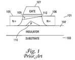
- FIG. 1illustrates a typical prior art SOI semiconductor.
- the transistoris formed in the silicon layer 101 that is over the insulator 102 .
- the insulatoris formed on top of the substrate 103 .
- the drain/source regions 105 and 106are formed within the silicon layer 101 .
- the gate 107is formed above the partially depleted channel 109 .
- a floating body 110is within the depleted region 112 and results from the partial depletion.
- the silicon film used for SOI transistorsmust be perfect crystalline silicon.
- the insulator layeris not crystalline. It is very difficult to make perfect crystalline silicon-on-oxide or silicon with other insulators since the insulator layer's crystalline properties are so different from the pure silicon. If perfect crystalline silicon is not obtained, defects will find their way onto the SOI film. This degrades the transistor performance.
- floating body effects in partially depleted CMOS devices using SOI technologyare undesirable in many logic and memory applications.
- the floating bodiescause threshold voltages and switching speeds to be variable and complex functions of the switching history of a particular logic gate.
- the floating bodiesIn dynamic logic and DRAM memories, the floating bodies cause excess charge leakage and short retention times that can cause data loss.
- the floating bodiescause reduced erase fields and slower erase times.
- FIG. 1shows a cross-sectional view of a typical prior art SOI semiconductor.
- FIG. 2shows a cross-sectional view of one embodiment for a planar NOR NROM cell using ultra-thin SOI.
- FIG. 3shows a cross-sectional view of one embodiment of two vertical NOR NROM cells of the present invention using ultra-thin SOI.
- FIG. 4shows a cross-sectional view of another embodiment of two vertical NOR NROM cells of the present invention using ultra-thin SOI.
- FIG. 5shows an electrical equivalent circuit of a NOR NROM flash memory array of the present invention.
- FIG. 6shows a cross-sectional view of yet another alternate embodiment of a vertical NOR NROM memory array of the present invention using ultra-thin SOI.
- FIG. 7shows an electrical equivalent circuit of a NOR NROM flash memory array of the present invention in accordance with the embodiment of FIG. 6 .
- FIG. 8shows a cross-sectional view of one embodiment of a planar NAND NROM cell of the present invention using ultra-thin SOI.
- FIG. 9shows a cross-sectional view of one embodiment of two vertical NAND NROM cells of the present invention using ultra-thin SOI.
- FIG. 10shows an electrical equivalent circuit of a NAND NROM flash memory array of the present invention in accordance with the embodiment of FIG. 9 .
- FIG. 11shows a block diagram of one embodiment of an electronic system of the present invention.
- FIG. 2illustrates a cross-sectional view of one embodiment of a planar NROM cell using ultra-thin silicon-on-insulator (SOI) technology.
- the NROM flash memory cell of FIG. 2is a NOR array cell with virtual ground bit lines.
- the NROM flash memory cellis comprised of the silicon layer 201 on the insulator 202 .
- the silicon 201 in an ultra-thin SOI cellis less than 100 nm (1000 ⁇ ).
- This layer 201is comprised of two source/drain areas 220 and 221 that act as bit lines 220 and 221 . In one embodiment, these areas 220 and 221 are n-type material. Alternate embodiments use p-type material if the substrate is an n-type material.
- the body region 200 between the bit lines 220 and 221is normally fully depleted in ultra-thin SOI.
- the body region 200is comprised of ionized acceptor impurities 203 and ionized donor impurities 205 .
- Two oxide areas 210 and 211are deposited on the silicon 201 .
- a gate insulator 207in one embodiment, is a composite structure of oxide-nitride-oxide (ONO) formed between the control gate 230 and the silicon layer 201 .
- the control gate 230in one embodiment, is a polysilicon material and extends in the ‘x’ direction in the NOR flash cell embodiment.
- the nitride layer 225has two charge storage areas 231 and 232 .
- Alternate embodiments of the present inventionuse other gate insulators besides the ONO composite structure shown. These structures may include oxide-nitride-aluminum oxide composite layers, oxide-aluminum oxide-oxide composite layers, oxide, silicon oxycarbide-oxide composite layers as well as other composite layers.
- the gate insulatormay include thicker than normal silicon oxides formed by wet oxidation and not annealed, silicon rich oxides with inclusions of nanoparticles of silicon, silicon oxynitride layer that are not composite layers, silicon rich aluminum oxide insulators that are not composite layers, silicon oxycarbide insulators that are not composite layers, silicon oxide insulators with inclusions of nanoparticles of silicon carbide, in addition to other non-stoichiometric single layers of gate insulators of two or more commonly used insulator materials such as Si, N, Al, Ti, Ta, Hf, Zr, and La.
- FIG. 3illustrates a cross-sectional view of one embodiment of two vertical NOR NROM cells 350 and 351 of the present invention using ultra-thin SOI.
- the vertical embodimentprovides for higher density memory arrays.
- the cells 350 and 351 of FIG. 3each have source/drain areas 330 and 331 that operate as bit lines and are comprised of n+ doped silicon. Alternate embodiments use p-type material if the substrate is comprised of n-type material. Additional source/drain areas 320 and 321 for each transistor are formed at the top of a vertical oxide pillar 310 .
- the left transistor 350uses source/drain areas 320 and 331 while the right transistor uses source/drain areas 321 and 330 .
- the upper source/drain areas 320 and 321are separated by a grain boundary but are electrically coupled.
- the vertical oxide pillar 310is an insulator between the two transistors 350 and 351 .
- Ultra-thin silicon 300 and 301are used to provide crystalline layers of ultra-thin silicon 300 and 301 along the sidewalls of the vertical oxide pillar 310 . These layers are the ultra-thin silicon (i.e., ⁇ 100 nm) body regions 300 and 301 and are normally fully depleted. The direction of thickness of the silicon body region 300 and 301 is illustrated in each region.
- the left ultra-thin silicon body regionis part of the left transistor 350 while the right body region 300 is part of the right transistor 351 .
- the gate insulator layer 307in one embodiment, is a composite ONO structure. Alternate embodiments of this layer 307 are disclosed above.
- the control gate 330is formed above this insulator layer 307 and is common to both transistors 350 and 351 such that it acts as a word line in a memory array. In one embodiment, the control gate 330 is a polysilicon material.
- FIG. 4illustrates a cross-sectional view of another embodiment of two vertical NOR NROM cells of the present invention using ultra-thin SOI.
- This embodimenthas an architecture that is substantially similar to the embodiment of FIG. 3 in that the ultra-thin silicon body regions 400 and 401 are formed by epitaxial regrowth along the sidewalls of the oxide pillar 410 .
- the top source/drain areas 420 and 421are formed at the top of the oxide pillar 410 and the common poly control gate 405 is formed over the gate insulator 407 coupling both transistors 450 and 451 by a word line.
- the bottom oxide layer 402 and 404 of the gate insulator 407is thicker in the trench than in the previous embodiment. Additionally, the two source/drain areas of FIG. 3 are replaced by a single n+ source/drain region 430 that is isolated between the portions of the thicker oxide layer.
- FIG. 5illustrates an electrical equivalent circuit of a NOR NROM flash memory array of the present invention. This circuit can represent the planar embodiments of the present invention as well as the vertical embodiment of FIG. 3 .
- the control gate 501crosses all of the devices 510 - 512 in the array.
- the n+ source/drain regions 503 and 504are used as virtual ground data or bit lines.
- the bit lines of the arrayare coupled to a sense amplifier in order to read data from the cells 510 - 512 .
- the control gate 501is the word line used to select the cells 510 - 512 .
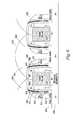
- FIG. 6illustrates a cross-sectional view of yet another alternate embodiment of a vertical NOR NROM memory array of the present invention using ultra-thin SOI.
- This figureillustrates four vertical transistors 650 - 653 .
- the transistors formed around the first oxide pillar 632are described.
- the remaining transistorsare substantially identical in structure and operation.
- the two ultra-thin silicon body regions 608 and 609are formed by epitaxial regrowth along the sidewalls of the oxide pillar 632 .
- the gate insulator layers 601 and 602are formed alongside of the silicon body regions 608 and 609 .
- the n+ polysilicon gate structures 630 and 631 for each transistor 650 and 651are then formed on the insulator layers 601 and 602 .
- the nitride layers 603 and 604provide two charge storage areas 610 and 611 for each transistor 650 - 653 .
- the lower oxide layer 605has a thicker composition than the rest of the gate insulator layer.
- the above cells 650 - 653are formed on a lower n+ region 620 on the substrate that acts as a common source/drain area, depending on the direction that each transistor is biased.
- the upper n+ regions 660 and 661are the second common source/drain area for each transistor 650 and 651 .
- the upper n+ region 660 and 661 of each transistoris coupled to other transistors in the array by a bonding wire 640 or other conductive device.
- FIG. 7illustrates an electrical equivalent circuit of a NOR NROM flash memory array of the present invention in accordance with the embodiment of FIG. 6 .
- This figureillustrates the respective cells 650 - 653 as described in FIG. 6 above.
- the control gates 701 - 704are coupled to other cells in the array and act as word lines. Two of these control gates 701 - 704 are illustrated in FIGS. 6 as 630 and 631 .
- the top common source/drain areas 660 and 661are shown as virtual ground or data bit line 709 while the common source/drain area 620 is shown as virtual ground or data bit line 708 .
- FIG. 8illustrates a cross-sectional view of one embodiment of a planar NAND NROM cell of the present invention using ultra-thin SOI.
- This embodimentis comprised of the two source/drain regions 803 and 804 with the fully depleted body region 801 in the ultra-thin SOI.
- the two oxide regions 807 and 808are formed above the n+ areas and the gate insulator 805 is formed over this architecture.
- the gate insulator 805is a composite ONO layer but can be any other type of material including those described above.
- the control gate 806is formed above the gate insulator 805 .
- the gate 806extends in the ‘z’ direction instead of the ‘x’ direction as in the NOR embodiment.
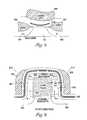
- FIG. 9illustrates a cross-sectional view of one embodiment of two vertical NAND NROM cells 910 and 911 of the present invention using ultra-thin SOI.
- Each transistor 910 and 911is comprised of a source/drain region 905 and 906 formed in a p-type substrate material.
- Second source/drain regions 920 and 921are formed on top of the oxide pillar 930 and separated by the grain boundary while still electrically coupled.
- the source/drain regions 905 , 906 , 920 , and 921function as electrical connections down the row.
- Epitaxial regrowthis used to grow ultra-thin silicon body regions 901 and 902 on the sidewalls of the oxide pillar 930 . As in previous embodiments, these regions 901 and 902 are each less than 100 nm thick.
- the gate insulator 950is formed on top of the transistors 910 and 911 .
- the gate insulator 950is an ONO composite layer. Alternate embodiments for the composition of this layer have been illustrated previously.
- Control gates 907 and 908 for each transistor 910 and 911 respectivelyare formed from a polysilicon material on each side of the gate insulator 950 .
- the control gates 907 and 908are coupled to other transistors to act as word lines.
- FIG. 10illustrates an electrical equivalent circuit of a NAND NROM flash memory array of the present invention in accordance with the embodiment of FIG. 9 .
- the two transistors 910 and 911 of FIG. 9are shown.
- the n+ source/drain connection 1005 of FIG. 10corresponds to the two source/drain regions 920 and 921 of FIG. 9 .
- the word lines 1001 and 1002 of FIG. 10correspond to the control gate 907 and 908 respectively of FIG. 9 .
- the source/drain regions 905 and 906 formed in the substrate of FIG. 9correspond to the source/drain connections 1009 and 1007 of FIG. 10 .
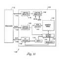
- FIG. 11illustrates a functional block diagram of a memory device 1100 that can incorporate the ultra-thin SOI flash memory cells of the present invention.
- the memory device 1100is coupled to a processor 1110 .
- the processor 1110may be a microprocessor or some other type of controlling circuitry.
- the memory device 1100 and the processor 1110form part of an electronic system 1120 .
- the memory device 1100has been simplified to focus on features of the memory that are helpful in understanding the present invention.
- the memory deviceincludes an array of flash memory cells 1130 .
- the memory cellsare NROM flash memory cells and the memory array 1130 is arranged in banks of rows and columns.
- the control gates of each row of memory cellsis coupled with a wordline while the drain and source connections of the memory cells are coupled to bitlines.
- bitlinesAs is well known in the art, the connection of the cells to the bitlines depends on whether the array is a NAND architecture or a NOR architecture.
- An address buffer circuit 1140is provided to latch address signals provided on address input connections A 0 -Ax 1142 . Address signals are received and decoded by a row decoder 1144 and a column decoder 1146 to access the memory array 1130 . It will be appreciated by those skilled in the art, with the benefit of the present description, that the number of address input connections depends on the density and architecture of the memory array 1130 . That is, the number of addresses increases with both increased memory cell counts and increased bank and block counts.
- the memory device 1100reads data in the memory array 1130 by sensing voltage or current changes in the memory array columns using sense/buffer circuitry 1150 .
- the sense/buffer circuitryin one embodiment, is coupled to read and latch a row of data from the memory array 1130 .
- Data input and output buffer circuitry 1160is included for bi-directional data communication over a plurality of data connections 1162 with the controller 1110 ).
- Write circuitry 1155is provided to write data to the memory array.
- Control circuitry 1170decodes signals provided on control connections 1172 from the processor 1110 . These signals are used to control the operations on the memory array 1130 , including data read, data write, and erase operations.
- the control circuitry 1170may be a state machine, a sequencer, or some other type of controller.
- the memory device 1100 of FIG. 11may be an embedded device with a CMOS processor.
- the flash memory device illustrated in FIG. 11has been simplified to facilitate a basic understanding of the features of the memory. A more detailed understanding of internal circuitry and functions of flash memories are known to those skilled in the art.
- the NROM flash memory cells of the present inventionutilize ultra-thin SOI to provide a fully depleted body region. This eliminates the undesirable floating body effects experienced by partially depleted CMOS devices.
Landscapes
- Engineering & Computer Science (AREA)
- Computer Hardware Design (AREA)
- Power Engineering (AREA)
- Microelectronics & Electronic Packaging (AREA)
- Physics & Mathematics (AREA)
- Manufacturing & Machinery (AREA)
- Condensed Matter Physics & Semiconductors (AREA)
- General Physics & Mathematics (AREA)
- Chemical Kinetics & Catalysis (AREA)
- Chemical & Material Sciences (AREA)
- General Chemical & Material Sciences (AREA)
- Crystallography & Structural Chemistry (AREA)
- Non-Volatile Memory (AREA)
- Semiconductor Memories (AREA)
- Thin Film Transistor (AREA)
Abstract
Description
Claims (20)
Priority Applications (2)
| Application Number | Priority Date | Filing Date | Title |
|---|---|---|---|
| US12/829,702US7915669B2 (en) | 2003-11-17 | 2010-07-02 | NROM flash memory devices on ultrathin silicon |
| US13/051,050US8183625B2 (en) | 2003-11-17 | 2011-03-18 | NROM flash memory devices on ultrathin silicon |
Applications Claiming Priority (5)
| Application Number | Priority Date | Filing Date | Title |
|---|---|---|---|
| US10/714,753US7202523B2 (en) | 2003-11-17 | 2003-11-17 | NROM flash memory devices on ultrathin silicon |
| US11/211,207US7276413B2 (en) | 2003-11-17 | 2005-08-25 | NROM flash memory devices on ultrathin silicon |
| US11/693,105US7378316B2 (en) | 2003-11-17 | 2007-03-29 | Method for fabricating semiconductor vertical NROM memory cells |
| US12/114,897US7768058B2 (en) | 2003-11-17 | 2008-05-05 | NROM flash memory devices on ultrathin silicon |
| US12/829,702US7915669B2 (en) | 2003-11-17 | 2010-07-02 | NROM flash memory devices on ultrathin silicon |
Related Parent Applications (1)
| Application Number | Title | Priority Date | Filing Date |
|---|---|---|---|
| US12/114,897ContinuationUS7768058B2 (en) | 2003-11-17 | 2008-05-05 | NROM flash memory devices on ultrathin silicon |
Related Child Applications (1)
| Application Number | Title | Priority Date | Filing Date |
|---|---|---|---|
| US13/051,050ContinuationUS8183625B2 (en) | 2003-11-17 | 2011-03-18 | NROM flash memory devices on ultrathin silicon |
Publications (2)
| Publication Number | Publication Date |
|---|---|
| US20100270610A1 US20100270610A1 (en) | 2010-10-28 |
| US7915669B2true US7915669B2 (en) | 2011-03-29 |
Family
ID=34574051
Family Applications (9)
| Application Number | Title | Priority Date | Filing Date |
|---|---|---|---|
| US10/714,753Expired - LifetimeUS7202523B2 (en) | 2003-11-17 | 2003-11-17 | NROM flash memory devices on ultrathin silicon |
| US11/211,207Expired - LifetimeUS7276413B2 (en) | 2003-11-17 | 2005-08-25 | NROM flash memory devices on ultrathin silicon |
| US11/211,208Expired - LifetimeUS7244987B2 (en) | 2003-11-17 | 2005-08-25 | NROM flash memory devices on ultrathin silicon |
| US11/211,201Expired - LifetimeUS7276762B2 (en) | 2003-11-17 | 2005-08-25 | NROM flash memory devices on ultrathin silicon |
| US11/693,150Expired - LifetimeUS7358562B2 (en) | 2003-11-17 | 2007-03-29 | NROM flash memory devices on ultrathin silicon |
| US11/693,105Expired - LifetimeUS7378316B2 (en) | 2003-11-17 | 2007-03-29 | Method for fabricating semiconductor vertical NROM memory cells |
| US12/114,897Expired - LifetimeUS7768058B2 (en) | 2003-11-17 | 2008-05-05 | NROM flash memory devices on ultrathin silicon |
| US12/829,702Expired - LifetimeUS7915669B2 (en) | 2003-11-17 | 2010-07-02 | NROM flash memory devices on ultrathin silicon |
| US13/051,050Expired - Fee RelatedUS8183625B2 (en) | 2003-11-17 | 2011-03-18 | NROM flash memory devices on ultrathin silicon |
Family Applications Before (7)
| Application Number | Title | Priority Date | Filing Date |
|---|---|---|---|
| US10/714,753Expired - LifetimeUS7202523B2 (en) | 2003-11-17 | 2003-11-17 | NROM flash memory devices on ultrathin silicon |
| US11/211,207Expired - LifetimeUS7276413B2 (en) | 2003-11-17 | 2005-08-25 | NROM flash memory devices on ultrathin silicon |
| US11/211,208Expired - LifetimeUS7244987B2 (en) | 2003-11-17 | 2005-08-25 | NROM flash memory devices on ultrathin silicon |
| US11/211,201Expired - LifetimeUS7276762B2 (en) | 2003-11-17 | 2005-08-25 | NROM flash memory devices on ultrathin silicon |
| US11/693,150Expired - LifetimeUS7358562B2 (en) | 2003-11-17 | 2007-03-29 | NROM flash memory devices on ultrathin silicon |
| US11/693,105Expired - LifetimeUS7378316B2 (en) | 2003-11-17 | 2007-03-29 | Method for fabricating semiconductor vertical NROM memory cells |
| US12/114,897Expired - LifetimeUS7768058B2 (en) | 2003-11-17 | 2008-05-05 | NROM flash memory devices on ultrathin silicon |
Family Applications After (1)
| Application Number | Title | Priority Date | Filing Date |
|---|---|---|---|
| US13/051,050Expired - Fee RelatedUS8183625B2 (en) | 2003-11-17 | 2011-03-18 | NROM flash memory devices on ultrathin silicon |
Country Status (7)
| Country | Link |
|---|---|
| US (9) | US7202523B2 (en) |
| EP (1) | EP1692728B1 (en) |
| JP (1) | JP2007534161A (en) |
| KR (2) | KR100813374B1 (en) |
| CN (1) | CN1883054A (en) |
| SG (1) | SG141431A1 (en) |
| WO (1) | WO2005050740A2 (en) |
Cited By (1)
| Publication number | Priority date | Publication date | Assignee | Title |
|---|---|---|---|---|
| US10199464B2 (en) | 2017-02-21 | 2019-02-05 | International Business Machines Corporation | Techniques for VFET top source/drain epitaxy |
Families Citing this family (50)
| Publication number | Priority date | Publication date | Assignee | Title |
|---|---|---|---|---|
| US7202523B2 (en)* | 2003-11-17 | 2007-04-10 | Micron Technology, Inc. | NROM flash memory devices on ultrathin silicon |
| US7183166B2 (en)* | 2003-11-25 | 2007-02-27 | Macronix International Co., Ltd. | Method for forming oxide on ONO structure |
| US20050156228A1 (en)* | 2004-01-16 | 2005-07-21 | Jeng Erik S. | Manufacture method and structure of a nonvolatile memory |
| KR100564628B1 (en)* | 2004-06-16 | 2006-03-28 | 삼성전자주식회사 | Split gate type flash memory device and manufacturing method thereof |
| US7138681B2 (en)* | 2004-07-27 | 2006-11-21 | Micron Technology, Inc. | High density stepped, non-planar nitride read only memory |
| US7518179B2 (en) | 2004-10-08 | 2009-04-14 | Freescale Semiconductor, Inc. | Virtual ground memory array and method therefor |
| KR100630746B1 (en)* | 2005-05-06 | 2006-10-02 | 삼성전자주식회사 | Multi-bit and multi-level nonvolatile memory device and its operation and manufacturing method |
| US7211858B2 (en)* | 2005-07-25 | 2007-05-01 | Freescale Semiconductor, Inc. | Split gate storage device including a horizontal first gate and a vertical second gate in a trench |
| US7394686B2 (en)* | 2005-07-25 | 2008-07-01 | Freescale Semiconductor, Inc. | Programmable structure including discontinuous storage elements and spacer control gates in a trench |
| US20070020840A1 (en)* | 2005-07-25 | 2007-01-25 | Freescale Semiconductor, Inc. | Programmable structure including nanocrystal storage elements in a trench |
| US7619270B2 (en)* | 2005-07-25 | 2009-11-17 | Freescale Semiconductor, Inc. | Electronic device including discontinuous storage elements |
| US7582929B2 (en)* | 2005-07-25 | 2009-09-01 | Freescale Semiconductor, Inc | Electronic device including discontinuous storage elements |
| US7226840B2 (en)* | 2005-07-25 | 2007-06-05 | Freescale Semiconductor, Inc. | Process for forming an electronic device including discontinuous storage elements |
| US7619275B2 (en)* | 2005-07-25 | 2009-11-17 | Freescale Semiconductor, Inc. | Process for forming an electronic device including discontinuous storage elements |
| US7262997B2 (en)* | 2005-07-25 | 2007-08-28 | Freescale Semiconductor, Inc. | Process for operating an electronic device including a memory array and conductive lines |
| US7285819B2 (en)* | 2005-07-25 | 2007-10-23 | Freescale Semiconductor, Inc. | Nonvolatile storage array with continuous control gate employing hot carrier injection programming |
| US7642594B2 (en)* | 2005-07-25 | 2010-01-05 | Freescale Semiconductor, Inc | Electronic device including gate lines, bit lines, or a combination thereof |
| US7205608B2 (en)* | 2005-07-25 | 2007-04-17 | Freescale Semiconductor, Inc. | Electronic device including discontinuous storage elements |
| US7314798B2 (en)* | 2005-07-25 | 2008-01-01 | Freescale Semiconductor, Inc. | Method of fabricating a nonvolatile storage array with continuous control gate employing hot carrier injection programming |
| US7211487B2 (en)* | 2005-07-25 | 2007-05-01 | Freescale Semiconductor, Inc. | Process for forming an electronic device including discontinuous storage elements |
| US7250340B2 (en)* | 2005-07-25 | 2007-07-31 | Freescale Semiconductor, Inc. | Method of fabricating programmable structure including discontinuous storage elements and spacer control gates in a trench |
| US7112490B1 (en)* | 2005-07-25 | 2006-09-26 | Freescale Semiconductor, Inc. | Hot carrier injection programmable structure including discontinuous storage elements and spacer control gates in a trench |
| US7256454B2 (en)* | 2005-07-25 | 2007-08-14 | Freescale Semiconductor, Inc | Electronic device including discontinuous storage elements and a process for forming the same |
| US7439576B2 (en)* | 2005-08-29 | 2008-10-21 | Micron Technology, Inc. | Ultra-thin body vertical tunneling transistor |
| US7446372B2 (en)* | 2005-09-01 | 2008-11-04 | Micron Technology, Inc. | DRAM tunneling access transistor |
| KR100685121B1 (en)* | 2005-10-14 | 2007-02-22 | 동부일렉트로닉스 주식회사 | Nonvolatile Memory Device and Manufacturing Method Thereof |
| US20070246765A1 (en)* | 2006-03-30 | 2007-10-25 | Lars Bach | Semiconductor memory device and method for production |
| US7592224B2 (en) | 2006-03-30 | 2009-09-22 | Freescale Semiconductor, Inc | Method of fabricating a storage device including decontinuous storage elements within and between trenches |
| JP5248819B2 (en)* | 2006-08-07 | 2013-07-31 | 三星電子株式会社 | Transistor and manufacturing method thereof |
| JP2008053270A (en)* | 2006-08-22 | 2008-03-06 | Nec Electronics Corp | Semiconductor memory device and manufacturing method thereof |
| US7880232B2 (en)* | 2006-11-01 | 2011-02-01 | Micron Technology, Inc. | Processes and apparatus having a semiconductor fin |
| JP2008166442A (en)* | 2006-12-27 | 2008-07-17 | Spansion Llc | Semiconductor device and manufacturing method thereof |
| US7572699B2 (en)* | 2007-01-24 | 2009-08-11 | Freescale Semiconductor, Inc | Process of forming an electronic device including fins and discontinuous storage elements |
| US7838922B2 (en)* | 2007-01-24 | 2010-11-23 | Freescale Semiconductor, Inc. | Electronic device including trenches and discontinuous storage elements |
| US7651916B2 (en)* | 2007-01-24 | 2010-01-26 | Freescale Semiconductor, Inc | Electronic device including trenches and discontinuous storage elements and processes of forming and using the same |
| US7416945B1 (en)* | 2007-02-19 | 2008-08-26 | Freescale Semiconductor, Inc. | Method for forming a split gate memory device |
| US7790560B2 (en)* | 2007-03-12 | 2010-09-07 | Board Of Regents Of The Nevada System Of Higher Education | Construction of flash memory chips and circuits from ordered nanoparticles |
| US8686487B2 (en) | 2007-06-14 | 2014-04-01 | Micron Technology, Inc. | Semiconductor devices and electronic systems comprising floating gate transistors |
| US7737488B2 (en)* | 2007-08-09 | 2010-06-15 | Macronix International Co., Ltd. | Blocking dielectric engineered charge trapping memory cell with high speed erase |
| US8320191B2 (en) | 2007-08-30 | 2012-11-27 | Infineon Technologies Ag | Memory cell arrangement, method for controlling a memory cell, memory array and electronic device |
| US8409952B2 (en)* | 2008-04-14 | 2013-04-02 | Spansion Llc | Method of forming an electronic device including forming a charge storage element in a trench of a workpiece |
| US8551858B2 (en)* | 2010-02-03 | 2013-10-08 | Spansion Llc | Self-aligned SI rich nitride charge trap layer isolation for charge trap flash memory |
| US8207032B2 (en) | 2010-08-31 | 2012-06-26 | Micron Technology, Inc. | Methods of forming pluralities of vertical transistors, and methods of forming memory arrays |
| CN102769016B (en)* | 2012-08-14 | 2015-01-14 | 北京大学 | Anti-radiation complementary metal oxide semiconductor (CMOS) device and preparation method thereof |
| KR102050561B1 (en)* | 2012-12-18 | 2020-01-09 | 삼성디스플레이 주식회사 | Vertical thin film transistor and fabrivating method thereof |
| US9093530B2 (en) | 2012-12-28 | 2015-07-28 | Taiwan Semiconductor Manufacturing Company, Ltd. | Fin structure of FinFET |
| US9082735B1 (en)* | 2014-08-14 | 2015-07-14 | Srikanth Sundararajan | 3-D silicon on glass based organic light emitting diode display |
| JP6100854B2 (en)* | 2014-11-19 | 2017-03-22 | 株式会社日立国際電気 | Semiconductor device manufacturing method, substrate processing apparatus, gas supply system, and program |
| US9385240B1 (en)* | 2015-03-03 | 2016-07-05 | Macronix International Co., Ltd. | Memory device and method for fabricating the same |
| US20170345834A1 (en)* | 2016-05-25 | 2017-11-30 | Globalfoundries Inc. | Soi memory device |
Citations (108)
| Publication number | Priority date | Publication date | Assignee | Title |
|---|---|---|---|---|
| US4184207A (en) | 1978-01-27 | 1980-01-15 | Texas Instruments Incorporated | High density floating gate electrically programmable ROM |
| US4420504A (en) | 1980-12-22 | 1983-12-13 | Raytheon Company | Programmable read only memory |
| US4755864A (en) | 1984-12-25 | 1988-07-05 | Kabushiki Kaisha Toshiba | Semiconductor read only memory device with selectively present mask layer |
| US4881114A (en) | 1986-05-16 | 1989-11-14 | Actel Corporation | Selectively formable vertical diode circuit element |
| US5241496A (en) | 1991-08-19 | 1993-08-31 | Micron Technology, Inc. | Array of read-only memory cells, eacch of which has a one-time, voltage-programmable antifuse element constructed within a trench shared by a pair of cells |
| US5330930A (en) | 1992-12-31 | 1994-07-19 | Chartered Semiconductor Manufacturing Pte Ltd. | Formation of vertical polysilicon resistor having a nitride sidewall for small static RAM cell |
| US5378647A (en) | 1993-10-25 | 1995-01-03 | United Microelectronics Corporation | Method of making a bottom gate mask ROM device |
| US5379253A (en) | 1992-06-01 | 1995-01-03 | National Semiconductor Corporation | High density EEPROM cell array with novel programming scheme and method of manufacture |
| US5397725A (en) | 1993-10-28 | 1995-03-14 | National Semiconductor Corporation | Method of controlling oxide thinning in an EPROM or flash memory array |
| US5467305A (en) | 1992-03-12 | 1995-11-14 | International Business Machines Corporation | Three-dimensional direct-write EEPROM arrays and fabrication methods |
| US5576236A (en) | 1995-06-28 | 1996-11-19 | United Microelectronics Corporation | Process for coding and code marking read-only memory |
| US5768192A (en) | 1996-07-23 | 1998-06-16 | Saifun Semiconductors, Ltd. | Non-volatile semiconductor memory cell utilizing asymmetrical charge trapping |
| US5792697A (en) | 1997-01-07 | 1998-08-11 | United Microelectronics Corporation | Method for fabricating a multi-stage ROM |
| US5811852A (en) | 1996-01-17 | 1998-09-22 | Advanced Materials Engineering Research, Inc. | Memory cell structure fabricated with improved fabrication process by forming dielectric layer directly on an insulated surface of a substrate |
| US5858841A (en) | 1997-01-20 | 1999-01-12 | United Microelectronics Corporation | ROM device having memory units arranged in three dimensions, and a method of making the same |
| US5911106A (en) | 1996-08-29 | 1999-06-08 | Nec Corporation | Semiconductor memory device and fabrication thereof |
| US5946558A (en) | 1997-02-05 | 1999-08-31 | United Microelectronics Corp. | Method of making ROM components |
| US5966603A (en) | 1997-06-11 | 1999-10-12 | Saifun Semiconductors Ltd. | NROM fabrication method with a periphery portion |
| US5973358A (en) | 1997-07-01 | 1999-10-26 | Citizen Watch Co., Ltd. | SOI device having a channel with variable thickness |
| US5994745A (en) | 1994-04-08 | 1999-11-30 | United Microelectronics Corp. | ROM device having shaped gate electrodes and corresponding code implants |
| US6011725A (en) | 1997-08-01 | 2000-01-04 | Saifun Semiconductors, Ltd. | Two bit non-volatile electrically erasable and programmable semiconductor memory cell utilizing asymmetrical charge trapping |
| US6028342A (en) | 1996-11-22 | 2000-02-22 | United Microelectronics Corp. | ROM diode and a method of making the same |
| US6030871A (en) | 1998-05-05 | 2000-02-29 | Saifun Semiconductors Ltd. | Process for producing two bit ROM cell utilizing angled implant |
| US6044022A (en) | 1999-02-26 | 2000-03-28 | Tower Semiconductor Ltd. | Programmable configuration for EEPROMS including 2-bit non-volatile memory cell arrays |
| US6081456A (en) | 1999-02-04 | 2000-06-27 | Tower Semiconductor Ltd. | Bit line control circuit for a memory array using 2-bit non-volatile memory cells |
| US6108240A (en) | 1999-02-04 | 2000-08-22 | Tower Semiconductor Ltd. | Implementation of EEPROM using intermediate gate voltage to avoid disturb conditions |
| US6134156A (en) | 1999-02-04 | 2000-10-17 | Saifun Semiconductors Ltd. | Method for initiating a retrieval procedure in virtual ground arrays |
| US6133102A (en) | 1998-06-19 | 2000-10-17 | Wu; Shye-Lin | Method of fabricating double poly-gate high density multi-state flat mask ROM cells |
| US6147904A (en) | 1999-02-04 | 2000-11-14 | Tower Semiconductor Ltd. | Redundancy method and structure for 2-bit non-volatile memory cells |
| US6157570A (en) | 1999-02-04 | 2000-12-05 | Tower Semiconductor Ltd. | Program/erase endurance of EEPROM memory cells |
| US6172396B1 (en) | 1998-02-03 | 2001-01-09 | Worldwide Semiconductor Manufacturing Corp. | ROM structure and method of manufacture |
| US6174758B1 (en) | 1999-03-03 | 2001-01-16 | Tower Semiconductor Ltd. | Semiconductor chip having fieldless array with salicide gates and methods for making same |
| US6175523B1 (en) | 1999-10-25 | 2001-01-16 | Advanced Micro Devices, Inc | Precharging mechanism and method for NAND-based flash memory devices |
| US6180461B1 (en) | 1998-08-03 | 2001-01-30 | Halo Lsi Design & Device Technology, Inc. | Double sidewall short channel split gate flash memory |
| US6181597B1 (en) | 1999-02-04 | 2001-01-30 | Tower Semiconductor Ltd. | EEPROM array using 2-bit non-volatile memory cells with serial read operations |
| US6184089B1 (en) | 1999-01-27 | 2001-02-06 | United Microelectronics Corp. | Method of fabricating one-time programmable read only memory |
| US6201737B1 (en) | 2000-01-28 | 2001-03-13 | Advanced Micro Devices, Inc. | Apparatus and method to characterize the threshold distribution in an NROM virtual ground array |
| US6204529B1 (en) | 1999-08-27 | 2001-03-20 | Hsing Lan Lung | 8 bit per cell non-volatile semiconductor memory structure utilizing trench technology and dielectric floating gate |
| US6207504B1 (en) | 1998-07-29 | 2001-03-27 | United Semiconductor Corp. | Method of fabricating flash erasable programmable read only memory |
| US6208557B1 (en) | 1999-05-21 | 2001-03-27 | National Semiconductor Corporation | EPROM and flash memory cells with source-side injection and a gate dielectric that traps hot electrons during programming |
| US6215702B1 (en) | 2000-02-16 | 2001-04-10 | Advanced Micro Devices, Inc. | Method of maintaining constant erasing speeds for non-volatile memory cells |
| US6218695B1 (en) | 1999-06-28 | 2001-04-17 | Tower Semiconductor Ltd. | Area efficient column select circuitry for 2-bit non-volatile memory cells |
| US6222768B1 (en) | 2000-01-28 | 2001-04-24 | Advanced Micro Devices, Inc. | Auto adjusting window placement scheme for an NROM virtual ground array |
| US20010001075A1 (en) | 1997-03-25 | 2001-05-10 | Vantis Corporation | Process for fabricating semiconductor memory device with high data retention including silicon nitride etch stop layer formed at high temperature with low hydrogen ion concentration |
| US6240020B1 (en) | 1999-10-25 | 2001-05-29 | Advanced Micro Devices | Method of bitline shielding in conjunction with a precharging scheme for nand-based flash memory devices |
| US6243300B1 (en) | 2000-02-16 | 2001-06-05 | Advanced Micro Devices, Inc. | Substrate hole injection for neutralizing spillover charge generated during programming of a non-volatile memory cell |
| US20010004332A1 (en) | 1998-05-20 | 2001-06-21 | Saifun Semiconductors Ltd. | NROM cell with improved programming, erasing and cycling |
| US6251731B1 (en) | 1998-08-10 | 2001-06-26 | Acer Semiconductor Manufacturing, Inc. | Method for fabricating high-density and high-speed nand-type mask roms |
| US6256231B1 (en) | 1999-02-04 | 2001-07-03 | Tower Semiconductor Ltd. | EEPROM array using 2-bit non-volatile memory cells and method of implementing same |
| US6255166B1 (en) | 1999-08-05 | 2001-07-03 | Aalo Lsi Design & Device Technology, Inc. | Nonvolatile memory cell, method of programming the same and nonvolatile memory array |
| US6266281B1 (en) | 2000-02-16 | 2001-07-24 | Advanced Micro Devices, Inc. | Method of erasing non-volatile memory cells |
| US6269023B1 (en) | 2000-05-19 | 2001-07-31 | Advanced Micro Devices, Inc. | Method of programming a non-volatile memory cell using a current limiter |
| US6272043B1 (en) | 2000-01-28 | 2001-08-07 | Advanced Micro Devices, Inc. | Apparatus and method of direct current sensing from source side in a virtual ground array |
| US6275414B1 (en) | 2000-05-16 | 2001-08-14 | Advanced Micro Devices, Inc. | Uniform bitline strapping of a non-volatile memory cell |
| US6282118B1 (en) | 2000-10-06 | 2001-08-28 | Macronix International Co. Ltd. | Nonvolatile semiconductor memory device |
| US6291854B1 (en) | 1999-12-30 | 2001-09-18 | United Microelectronics Corp. | Electrically erasable and programmable read only memory device and manufacturing therefor |
| US6297096B1 (en) | 1997-06-11 | 2001-10-02 | Saifun Semiconductors Ltd. | NROM fabrication method |
| US6303436B1 (en) | 1999-09-21 | 2001-10-16 | Mosel Vitelic, Inc. | Method for fabricating a type of trench mask ROM cell |
| US6327174B1 (en) | 2000-02-14 | 2001-12-04 | United Microelectronics Corp. | Method of manufacturing mask read-only memory cell |
| US6348711B1 (en) | 1998-05-20 | 2002-02-19 | Saifun Semiconductors Ltd. | NROM cell with self-aligned programming and erasure areas |
| US20020043682A1 (en) | 1997-08-29 | 2002-04-18 | Semiconductor Energy Laboratory Co., Ltd. | Non-volatile memory and semiconductor device |
| US6417053B1 (en) | 2001-11-20 | 2002-07-09 | Macronix International Co., Ltd. | Fabrication method for a silicon nitride read-only memory |
| US6421275B1 (en) | 2002-01-22 | 2002-07-16 | Macronix International Co. Ltd. | Method for adjusting a reference current of a flash nitride read only memory (NROM) and device thereof |
| US6424001B1 (en) | 2001-02-09 | 2002-07-23 | Micron Technology, Inc. | Flash memory with ultra thin vertical body transistors |
| US6429063B1 (en) | 1999-10-26 | 2002-08-06 | Saifun Semiconductors Ltd. | NROM cell with generally decoupled primary and secondary injection |
| US6432778B1 (en) | 2001-08-07 | 2002-08-13 | Macronix International Co. Ltd. | Method of forming a system on chip (SOC) with nitride read only memory (NROM) |
| US20020142569A1 (en) | 2001-03-29 | 2002-10-03 | Chang Kent Kuohua | Method for fabricating a nitride read-only -memory (nrom) |
| US20020146885A1 (en) | 2001-04-04 | 2002-10-10 | Chia-Hsing Chen | Method of fabricating a nitride read only memory cell |
| US20020151138A1 (en) | 2001-04-13 | 2002-10-17 | Chien-Hung Liu | Method for fabricating an NROM |
| US6468864B1 (en) | 2001-06-21 | 2002-10-22 | Macronix International Co., Ltd. | Method of fabricating silicon nitride read only memory |
| US6469342B1 (en) | 2001-10-29 | 2002-10-22 | Macronix International Co., Ltd. | Silicon nitride read only memory that prevents antenna effect |
| US20020168875A1 (en) | 2001-05-10 | 2002-11-14 | Chang Kent Kuohua | Method for fabricating an ONO layer of an NROM |
| US6486028B1 (en) | 2001-11-20 | 2002-11-26 | Macronix International Co., Ltd. | Method of fabricating a nitride read-only-memory cell vertical structure |
| US6487050B1 (en) | 1999-02-22 | 2002-11-26 | Seagate Technology Llc | Disc drive with wear-resistant ramp coating of carbon nitride or metal nitride |
| US20020177275A1 (en) | 2001-05-28 | 2002-11-28 | Chien-Hung Liu | Fabrication method for a silicon nitride read-only memory |
| US20020182829A1 (en) | 2001-05-31 | 2002-12-05 | Chia-Hsing Chen | Method for forming nitride read only memory with indium pocket region |
| US6496034B2 (en) | 2001-02-09 | 2002-12-17 | Micron Technology, Inc. | Programmable logic arrays with ultra thin body transistors |
| US6498377B1 (en) | 2002-03-21 | 2002-12-24 | Macronix International, Co., Ltd. | SONOS component having high dielectric property |
| US6514831B1 (en) | 2001-11-14 | 2003-02-04 | Macronix International Co., Ltd. | Nitride read only memory cell |
| WO2003017374A2 (en) | 2001-08-06 | 2003-02-27 | Infineon Technologies Ag | Memory cell |
| US20030040152A1 (en) | 2001-08-22 | 2003-02-27 | Chen-Chin Liu | Method of fabricating a NROM cell to prevent charging |
| US6531887B2 (en) | 2001-06-01 | 2003-03-11 | Macronix International Co., Ltd. | One cell programmable switch using non-volatile cell |
| US6545309B1 (en) | 2002-03-11 | 2003-04-08 | Macronix International Co., Ltd. | Nitride read-only memory with protective diode and operating method thereof |
| US20030067807A1 (en) | 2001-09-28 | 2003-04-10 | Hung-Sui Lin | Erasing method for p-channel NROM |
| US6552387B1 (en) | 1997-07-30 | 2003-04-22 | Saifun Semiconductors Ltd. | Non-volatile electrically erasable and programmable semiconductor memory cell utilizing asymmetrical charge trapping |
| US6559013B1 (en) | 2002-06-20 | 2003-05-06 | Macronix International Co., Ltd. | Method for fabricating mask ROM device |
| US6576511B2 (en) | 2001-05-02 | 2003-06-10 | Macronix International Co., Ltd. | Method for forming nitride read only memory |
| US6580135B2 (en) | 2001-06-18 | 2003-06-17 | Macronix International Co., Ltd. | Silicon nitride read only memory structure and method of programming and erasure |
| US6580630B1 (en) | 2002-04-02 | 2003-06-17 | Macronix International Co., Ltd. | Initialization method of P-type silicon nitride read only memory |
| US20030117861A1 (en) | 2001-12-20 | 2003-06-26 | Eduardo Maayan | NROM NOR array |
| US6602805B2 (en) | 2000-12-14 | 2003-08-05 | Macronix International Co., Ltd. | Method for forming gate dielectric layer in NROM |
| US6607957B1 (en) | 2002-07-31 | 2003-08-19 | Macronix International Co., Ltd. | Method for fabricating nitride read only memory |
| US6610586B1 (en) | 2002-09-04 | 2003-08-26 | Macronix International Co., Ltd. | Method for fabricating nitride read-only memory |
| US6617204B2 (en) | 2001-08-13 | 2003-09-09 | Macronix International Co., Ltd. | Method of forming the protective film to prevent nitride read only memory cell charging |
| US20030183873A1 (en) | 1998-11-04 | 2003-10-02 | Ichiro Fujiwara | Nonvolatile semiconductor memory device and process of production and write method thereof |
| US6657252B2 (en) | 2002-03-19 | 2003-12-02 | International Business Machines Corporation | FinFET CMOS with NVRAM capability |
| US20030222294A1 (en) | 2002-05-29 | 2003-12-04 | Nec Electronics Corporation | Nonvolatile semiconductor storage device |
| US6664143B2 (en) | 2000-11-22 | 2003-12-16 | North Carolina State University | Methods of fabricating vertical field effect transistors by conformal channel layer deposition on sidewalls |
| US6830963B1 (en) | 2003-10-09 | 2004-12-14 | Micron Technology, Inc. | Fully depleted silicon-on-insulator CMOS logic |
| US20050023574A1 (en)* | 2002-07-08 | 2005-02-03 | Micron Technology, Inc. | Memory utilizing oxide-nitride nanolaminates |
| US6906390B2 (en) | 2000-10-26 | 2005-06-14 | Sony Corporation | Nonvolatile semiconductor storage and method for manufacturing the same |
| US6943402B2 (en) | 2003-05-30 | 2005-09-13 | Kabushiki Kaisha Toshiba | Nonvolatile semiconductor memory device including MOS transistors each having a floating gate and control gate |
| US6949788B2 (en) | 1999-12-17 | 2005-09-27 | Sony Corporation | Nonvolatile semiconductor memory device and method for operating the same |
| US7138681B2 (en) | 2004-07-27 | 2006-11-21 | Micron Technology, Inc. | High density stepped, non-planar nitride read only memory |
| US20070034922A1 (en)* | 2005-08-11 | 2007-02-15 | Micron Technology, Inc. | Integrated surround gate multifunctional memory device |
| US20080099830A1 (en)* | 2006-11-01 | 2008-05-01 | Macronix International Co., Ltd. | Cylindrical channel charge trapping devices with effectively high coupling ratios |
| US20090085088A1 (en)* | 2007-09-28 | 2009-04-02 | Elpida Memory, Inc. | Semiconductor device and method of forming the same as well as data processing system including the semiconductor device |
| US20090256187A1 (en)* | 2008-04-10 | 2009-10-15 | Kyung Do Kim | Semiconductor device having vertical pillar transistors and method for manufacturing the same |
Family Cites Families (38)
| Publication number | Priority date | Publication date | Assignee | Title |
|---|---|---|---|---|
| US4513494A (en) | 1983-07-19 | 1985-04-30 | American Microsystems, Incorporated | Late mask process for programming read only memories |
| FR2640428B1 (en)* | 1988-12-09 | 1992-10-30 | Thomson Csf | METHOD OF HARDENING WITH RESPECT TO IONIZING RADIATION OF ACTIVE ELECTRONIC COMPONENTS, AND HARDENED COMPONENTS OF LARGE DIMENSIONS |
| JP2509706B2 (en) | 1989-08-18 | 1996-06-26 | 株式会社東芝 | Mask ROM manufacturing method |
| US5547236A (en)* | 1995-02-23 | 1996-08-20 | Gregory; John E. | Removable door lock |
| JP3524213B2 (en)* | 1995-06-07 | 2004-05-10 | 株式会社ルネサステクノロジ | Semiconductor memory device and method of manufacturing the same |
| US5994765A (en)* | 1996-07-01 | 1999-11-30 | Sun Microsystems, Inc. | Clock distribution network with efficient shielding |
| US6281695B1 (en)* | 1996-12-17 | 2001-08-28 | Robbie M. K. Chung | Integrated circuit package pin indicator |
| US5990509A (en)* | 1997-01-22 | 1999-11-23 | International Business Machines Corporation | 2F-square memory cell for gigabit memory applications |
| US6034389A (en)* | 1997-01-22 | 2000-03-07 | International Business Machines Corporation | Self-aligned diffused source vertical transistors with deep trench capacitors in a 4F-square memory cell array |
| WO1998047044A1 (en)* | 1997-04-11 | 1998-10-22 | Hitachi, Ltd. | Liquid crystal display device |
| US6124729A (en)* | 1998-02-27 | 2000-09-26 | Micron Technology, Inc. | Field programmable logic arrays with vertical transistors |
| US5991225A (en)* | 1998-02-27 | 1999-11-23 | Micron Technology, Inc. | Programmable memory address decode array with vertical transistors |
| US6468684B1 (en)* | 1999-01-22 | 2002-10-22 | California Institute Of Technology | Proton conducting membrane using a solid acid |
| JP2001085422A (en)* | 1999-09-17 | 2001-03-30 | Tokyo Electron Ltd | Method of forming laminated gate insulating film and system for forming the same |
| US6941644B2 (en)* | 1999-09-27 | 2005-09-13 | Reliance Electric Technologies, Llc | Method for winding segments of a segmented wound member of an electromechanical device |
| FR2799570B1 (en)* | 1999-10-08 | 2001-11-16 | Itt Mfg Enterprises Inc | IMPROVED ELECTRICAL SWITCH WITH MULTI-WAY TACTILE EFFECT AND SINGLE TRIGGER |
| JP3578688B2 (en)* | 1999-12-24 | 2004-10-20 | Necエレクトロニクス株式会社 | Manufacturing method of nonvolatile memory |
| JP2001326289A (en)* | 2000-03-08 | 2001-11-22 | Semiconductor Energy Lab Co Ltd | Nonvolatile memory and semiconductor device |
| US6273043B1 (en)* | 2000-03-16 | 2001-08-14 | Raymond A. Barton | Mounting plate and rocker arm assembly |
| KR100821456B1 (en)* | 2000-08-14 | 2008-04-11 | 샌디스크 쓰리디 엘엘씨 | Dense array and charge storage device and manufacturing method thereof |
| JP3984020B2 (en)* | 2000-10-30 | 2007-09-26 | 株式会社東芝 | Nonvolatile semiconductor memory device |
| US6566682B2 (en)* | 2001-02-09 | 2003-05-20 | Micron Technology, Inc. | Programmable memory address and decode circuits with ultra thin vertical body transistors |
| EP1263051A1 (en) | 2001-05-30 | 2002-12-04 | Infineon Technologies AG | Bitline contacts in a memory cell array |
| JP4198903B2 (en)* | 2001-08-31 | 2008-12-17 | 株式会社東芝 | Semiconductor memory device |
| US6903977B2 (en)* | 2001-09-25 | 2005-06-07 | Sony Corporation | Nonvolatile semiconductor memory device and method of producing the same |
| JP2003142610A (en)* | 2001-11-07 | 2003-05-16 | Sony Corp | Nonvolatile semiconductor memory device and method for injecting charge thereof |
| JP2003218242A (en)* | 2002-01-24 | 2003-07-31 | Hitachi Ltd | Nonvolatile semiconductor memory device and method of manufacturing the same |
| JP4472934B2 (en)* | 2002-03-27 | 2010-06-02 | イノテック株式会社 | Semiconductor device and semiconductor memory |
| US20040157466A1 (en)* | 2003-02-12 | 2004-08-12 | Songlin Xu | Methods of forming polymer films and of using such polymer films to form structures on substrates |
| JP2004356207A (en)* | 2003-05-27 | 2004-12-16 | Fujio Masuoka | Semiconductor storage device and method of manufacturing the same |
| US6977412B2 (en)* | 2003-09-05 | 2005-12-20 | Micron Technology, Inc. | Trench corner effect bidirectional flash memory cell |
| US7184315B2 (en)* | 2003-11-04 | 2007-02-27 | Micron Technology, Inc. | NROM flash memory with self-aligned structural charge separation |
| US7202523B2 (en)* | 2003-11-17 | 2007-04-10 | Micron Technology, Inc. | NROM flash memory devices on ultrathin silicon |
| US7388251B2 (en)* | 2004-08-11 | 2008-06-17 | Micron Technology, Inc. | Non-planar flash memory array with shielded floating gates on silicon mesas |
| US7312495B2 (en)* | 2005-04-07 | 2007-12-25 | Spansion Llc | Split gate multi-bit memory cell |
| US20060273370A1 (en)* | 2005-06-07 | 2006-12-07 | Micron Technology, Inc. | NROM flash memory with vertical transistors and surrounding gates |
| US8734583B2 (en)* | 2006-04-04 | 2014-05-27 | Micron Technology, Inc. | Grown nanofin transistors |
| KR100764745B1 (en)* | 2006-08-31 | 2007-10-08 | 삼성전자주식회사 | Semiconductor device having semi-cylindrical active region and manufacturing method thereof |
- 2003
- 2003-11-17USUS10/714,753patent/US7202523B2/ennot_activeExpired - Lifetime
- 2004
- 2004-11-16CNCNA2004800338366Apatent/CN1883054A/enactivePending
- 2004-11-16JPJP2006541306Apatent/JP2007534161A/enactivePending
- 2004-11-16EPEP04811109.0Apatent/EP1692728B1/ennot_activeExpired - Lifetime
- 2004-11-16SGSG200801927-5Apatent/SG141431A1/enunknown
- 2004-11-16KRKR1020077017396Apatent/KR100813374B1/ennot_activeExpired - Lifetime
- 2004-11-16WOPCT/US2004/038261patent/WO2005050740A2/enactiveApplication Filing
- 2004-11-16KRKR1020067009516Apatent/KR100813373B1/ennot_activeExpired - Lifetime
- 2005
- 2005-08-25USUS11/211,207patent/US7276413B2/ennot_activeExpired - Lifetime
- 2005-08-25USUS11/211,208patent/US7244987B2/ennot_activeExpired - Lifetime
- 2005-08-25USUS11/211,201patent/US7276762B2/ennot_activeExpired - Lifetime
- 2007
- 2007-03-29USUS11/693,150patent/US7358562B2/ennot_activeExpired - Lifetime
- 2007-03-29USUS11/693,105patent/US7378316B2/ennot_activeExpired - Lifetime
- 2008
- 2008-05-05USUS12/114,897patent/US7768058B2/ennot_activeExpired - Lifetime
- 2010
- 2010-07-02USUS12/829,702patent/US7915669B2/ennot_activeExpired - Lifetime
- 2011
- 2011-03-18USUS13/051,050patent/US8183625B2/ennot_activeExpired - Fee Related
Patent Citations (118)
| Publication number | Priority date | Publication date | Assignee | Title |
|---|---|---|---|---|
| US4184207A (en) | 1978-01-27 | 1980-01-15 | Texas Instruments Incorporated | High density floating gate electrically programmable ROM |
| US4420504A (en) | 1980-12-22 | 1983-12-13 | Raytheon Company | Programmable read only memory |
| US4755864A (en) | 1984-12-25 | 1988-07-05 | Kabushiki Kaisha Toshiba | Semiconductor read only memory device with selectively present mask layer |
| US4881114A (en) | 1986-05-16 | 1989-11-14 | Actel Corporation | Selectively formable vertical diode circuit element |
| US5241496A (en) | 1991-08-19 | 1993-08-31 | Micron Technology, Inc. | Array of read-only memory cells, eacch of which has a one-time, voltage-programmable antifuse element constructed within a trench shared by a pair of cells |
| US5467305A (en) | 1992-03-12 | 1995-11-14 | International Business Machines Corporation | Three-dimensional direct-write EEPROM arrays and fabrication methods |
| US5379253A (en) | 1992-06-01 | 1995-01-03 | National Semiconductor Corporation | High density EEPROM cell array with novel programming scheme and method of manufacture |
| US5330930A (en) | 1992-12-31 | 1994-07-19 | Chartered Semiconductor Manufacturing Pte Ltd. | Formation of vertical polysilicon resistor having a nitride sidewall for small static RAM cell |
| US5378647A (en) | 1993-10-25 | 1995-01-03 | United Microelectronics Corporation | Method of making a bottom gate mask ROM device |
| US5397725A (en) | 1993-10-28 | 1995-03-14 | National Semiconductor Corporation | Method of controlling oxide thinning in an EPROM or flash memory array |
| US5994745A (en) | 1994-04-08 | 1999-11-30 | United Microelectronics Corp. | ROM device having shaped gate electrodes and corresponding code implants |
| US5576236A (en) | 1995-06-28 | 1996-11-19 | United Microelectronics Corporation | Process for coding and code marking read-only memory |
| US5811852A (en) | 1996-01-17 | 1998-09-22 | Advanced Materials Engineering Research, Inc. | Memory cell structure fabricated with improved fabrication process by forming dielectric layer directly on an insulated surface of a substrate |
| US5768192A (en) | 1996-07-23 | 1998-06-16 | Saifun Semiconductors, Ltd. | Non-volatile semiconductor memory cell utilizing asymmetrical charge trapping |
| US20010011755A1 (en) | 1996-08-29 | 2001-08-09 | Kazuhiro Tasaka | Semiconductor memory device and fabrication thereof |
| US5911106A (en) | 1996-08-29 | 1999-06-08 | Nec Corporation | Semiconductor memory device and fabrication thereof |
| US6028342A (en) | 1996-11-22 | 2000-02-22 | United Microelectronics Corp. | ROM diode and a method of making the same |
| US5792697A (en) | 1997-01-07 | 1998-08-11 | United Microelectronics Corporation | Method for fabricating a multi-stage ROM |
| US5858841A (en) | 1997-01-20 | 1999-01-12 | United Microelectronics Corporation | ROM device having memory units arranged in three dimensions, and a method of making the same |
| US5946558A (en) | 1997-02-05 | 1999-08-31 | United Microelectronics Corp. | Method of making ROM components |
| US20010001075A1 (en) | 1997-03-25 | 2001-05-10 | Vantis Corporation | Process for fabricating semiconductor memory device with high data retention including silicon nitride etch stop layer formed at high temperature with low hydrogen ion concentration |
| US5966603A (en) | 1997-06-11 | 1999-10-12 | Saifun Semiconductors Ltd. | NROM fabrication method with a periphery portion |
| US6297096B1 (en) | 1997-06-11 | 2001-10-02 | Saifun Semiconductors Ltd. | NROM fabrication method |
| US5973358A (en) | 1997-07-01 | 1999-10-26 | Citizen Watch Co., Ltd. | SOI device having a channel with variable thickness |
| US6552387B1 (en) | 1997-07-30 | 2003-04-22 | Saifun Semiconductors Ltd. | Non-volatile electrically erasable and programmable semiconductor memory cell utilizing asymmetrical charge trapping |
| US6011725A (en) | 1997-08-01 | 2000-01-04 | Saifun Semiconductors, Ltd. | Two bit non-volatile electrically erasable and programmable semiconductor memory cell utilizing asymmetrical charge trapping |
| US20020043682A1 (en) | 1997-08-29 | 2002-04-18 | Semiconductor Energy Laboratory Co., Ltd. | Non-volatile memory and semiconductor device |
| US6172396B1 (en) | 1998-02-03 | 2001-01-09 | Worldwide Semiconductor Manufacturing Corp. | ROM structure and method of manufacture |
| US6030871A (en) | 1998-05-05 | 2000-02-29 | Saifun Semiconductors Ltd. | Process for producing two bit ROM cell utilizing angled implant |
| US6201282B1 (en) | 1998-05-05 | 2001-03-13 | Saifun Semiconductors Ltd. | Two bit ROM cell and process for producing same |
| US20010004332A1 (en) | 1998-05-20 | 2001-06-21 | Saifun Semiconductors Ltd. | NROM cell with improved programming, erasing and cycling |
| US6348711B1 (en) | 1998-05-20 | 2002-02-19 | Saifun Semiconductors Ltd. | NROM cell with self-aligned programming and erasure areas |
| US6477084B2 (en) | 1998-05-20 | 2002-11-05 | Saifun Semiconductors Ltd. | NROM cell with improved programming, erasing and cycling |
| US6133102A (en) | 1998-06-19 | 2000-10-17 | Wu; Shye-Lin | Method of fabricating double poly-gate high density multi-state flat mask ROM cells |
| US6207504B1 (en) | 1998-07-29 | 2001-03-27 | United Semiconductor Corp. | Method of fabricating flash erasable programmable read only memory |
| US6180461B1 (en) | 1998-08-03 | 2001-01-30 | Halo Lsi Design & Device Technology, Inc. | Double sidewall short channel split gate flash memory |
| US6580116B2 (en) | 1998-08-03 | 2003-06-17 | Halo Lsi, Inc. | Double sidewall short channel split gate flash memory |
| US6251731B1 (en) | 1998-08-10 | 2001-06-26 | Acer Semiconductor Manufacturing, Inc. | Method for fabricating high-density and high-speed nand-type mask roms |
| US6794712B1 (en) | 1998-11-04 | 2004-09-21 | Sony Corporation | Nonvolatile semiconductor memory device and process of production and write method thereof |
| US20030183873A1 (en) | 1998-11-04 | 2003-10-02 | Ichiro Fujiwara | Nonvolatile semiconductor memory device and process of production and write method thereof |
| US6184089B1 (en) | 1999-01-27 | 2001-02-06 | United Microelectronics Corp. | Method of fabricating one-time programmable read only memory |
| US6108240A (en) | 1999-02-04 | 2000-08-22 | Tower Semiconductor Ltd. | Implementation of EEPROM using intermediate gate voltage to avoid disturb conditions |
| US6147904A (en) | 1999-02-04 | 2000-11-14 | Tower Semiconductor Ltd. | Redundancy method and structure for 2-bit non-volatile memory cells |
| US6081456A (en) | 1999-02-04 | 2000-06-27 | Tower Semiconductor Ltd. | Bit line control circuit for a memory array using 2-bit non-volatile memory cells |
| US6134156A (en) | 1999-02-04 | 2000-10-17 | Saifun Semiconductors Ltd. | Method for initiating a retrieval procedure in virtual ground arrays |
| US6256231B1 (en) | 1999-02-04 | 2001-07-03 | Tower Semiconductor Ltd. | EEPROM array using 2-bit non-volatile memory cells and method of implementing same |
| US6181597B1 (en) | 1999-02-04 | 2001-01-30 | Tower Semiconductor Ltd. | EEPROM array using 2-bit non-volatile memory cells with serial read operations |
| US6157570A (en) | 1999-02-04 | 2000-12-05 | Tower Semiconductor Ltd. | Program/erase endurance of EEPROM memory cells |
| US6487050B1 (en) | 1999-02-22 | 2002-11-26 | Seagate Technology Llc | Disc drive with wear-resistant ramp coating of carbon nitride or metal nitride |
| US6044022A (en) | 1999-02-26 | 2000-03-28 | Tower Semiconductor Ltd. | Programmable configuration for EEPROMS including 2-bit non-volatile memory cell arrays |
| US6174758B1 (en) | 1999-03-03 | 2001-01-16 | Tower Semiconductor Ltd. | Semiconductor chip having fieldless array with salicide gates and methods for making same |
| US6208557B1 (en) | 1999-05-21 | 2001-03-27 | National Semiconductor Corporation | EPROM and flash memory cells with source-side injection and a gate dielectric that traps hot electrons during programming |
| US6218695B1 (en) | 1999-06-28 | 2001-04-17 | Tower Semiconductor Ltd. | Area efficient column select circuitry for 2-bit non-volatile memory cells |
| US6255166B1 (en) | 1999-08-05 | 2001-07-03 | Aalo Lsi Design & Device Technology, Inc. | Nonvolatile memory cell, method of programming the same and nonvolatile memory array |
| US6204529B1 (en) | 1999-08-27 | 2001-03-20 | Hsing Lan Lung | 8 bit per cell non-volatile semiconductor memory structure utilizing trench technology and dielectric floating gate |
| US6303436B1 (en) | 1999-09-21 | 2001-10-16 | Mosel Vitelic, Inc. | Method for fabricating a type of trench mask ROM cell |
| US6240020B1 (en) | 1999-10-25 | 2001-05-29 | Advanced Micro Devices | Method of bitline shielding in conjunction with a precharging scheme for nand-based flash memory devices |
| US6175523B1 (en) | 1999-10-25 | 2001-01-16 | Advanced Micro Devices, Inc | Precharging mechanism and method for NAND-based flash memory devices |
| US6429063B1 (en) | 1999-10-26 | 2002-08-06 | Saifun Semiconductors Ltd. | NROM cell with generally decoupled primary and secondary injection |
| US6949788B2 (en) | 1999-12-17 | 2005-09-27 | Sony Corporation | Nonvolatile semiconductor memory device and method for operating the same |
| US6291854B1 (en) | 1999-12-30 | 2001-09-18 | United Microelectronics Corp. | Electrically erasable and programmable read only memory device and manufacturing therefor |
| US6201737B1 (en) | 2000-01-28 | 2001-03-13 | Advanced Micro Devices, Inc. | Apparatus and method to characterize the threshold distribution in an NROM virtual ground array |
| US6222768B1 (en) | 2000-01-28 | 2001-04-24 | Advanced Micro Devices, Inc. | Auto adjusting window placement scheme for an NROM virtual ground array |
| US6272043B1 (en) | 2000-01-28 | 2001-08-07 | Advanced Micro Devices, Inc. | Apparatus and method of direct current sensing from source side in a virtual ground array |
| US6327174B1 (en) | 2000-02-14 | 2001-12-04 | United Microelectronics Corp. | Method of manufacturing mask read-only memory cell |
| US6392930B2 (en) | 2000-02-14 | 2002-05-21 | United Microelectronics Corp. | Method of manufacturing mask read-only memory cell |
| US6266281B1 (en) | 2000-02-16 | 2001-07-24 | Advanced Micro Devices, Inc. | Method of erasing non-volatile memory cells |
| US6243300B1 (en) | 2000-02-16 | 2001-06-05 | Advanced Micro Devices, Inc. | Substrate hole injection for neutralizing spillover charge generated during programming of a non-volatile memory cell |
| US6215702B1 (en) | 2000-02-16 | 2001-04-10 | Advanced Micro Devices, Inc. | Method of maintaining constant erasing speeds for non-volatile memory cells |
| US6275414B1 (en) | 2000-05-16 | 2001-08-14 | Advanced Micro Devices, Inc. | Uniform bitline strapping of a non-volatile memory cell |
| US6269023B1 (en) | 2000-05-19 | 2001-07-31 | Advanced Micro Devices, Inc. | Method of programming a non-volatile memory cell using a current limiter |
| US6282118B1 (en) | 2000-10-06 | 2001-08-28 | Macronix International Co. Ltd. | Nonvolatile semiconductor memory device |
| US6906390B2 (en) | 2000-10-26 | 2005-06-14 | Sony Corporation | Nonvolatile semiconductor storage and method for manufacturing the same |
| US6664143B2 (en) | 2000-11-22 | 2003-12-16 | North Carolina State University | Methods of fabricating vertical field effect transistors by conformal channel layer deposition on sidewalls |
| US6602805B2 (en) | 2000-12-14 | 2003-08-05 | Macronix International Co., Ltd. | Method for forming gate dielectric layer in NROM |
| US6424001B1 (en) | 2001-02-09 | 2002-07-23 | Micron Technology, Inc. | Flash memory with ultra thin vertical body transistors |
| US6496034B2 (en) | 2001-02-09 | 2002-12-17 | Micron Technology, Inc. | Programmable logic arrays with ultra thin body transistors |
| US6461949B1 (en) | 2001-03-29 | 2002-10-08 | Macronix International Co. Ltd. | Method for fabricating a nitride read-only-memory (NROM) |
| US20020142569A1 (en) | 2001-03-29 | 2002-10-03 | Chang Kent Kuohua | Method for fabricating a nitride read-only -memory (nrom) |
| US20020146885A1 (en) | 2001-04-04 | 2002-10-10 | Chia-Hsing Chen | Method of fabricating a nitride read only memory cell |
| US20020151138A1 (en) | 2001-04-13 | 2002-10-17 | Chien-Hung Liu | Method for fabricating an NROM |
| US6576511B2 (en) | 2001-05-02 | 2003-06-10 | Macronix International Co., Ltd. | Method for forming nitride read only memory |
| US20020168875A1 (en) | 2001-05-10 | 2002-11-14 | Chang Kent Kuohua | Method for fabricating an ONO layer of an NROM |
| US6548425B2 (en) | 2001-05-10 | 2003-04-15 | Macronix International Co. Ltd. | Method for fabricating an ONO layer of an NROM |
| US6613632B2 (en) | 2001-05-28 | 2003-09-02 | Macronix International Co., Ltd. | Fabrication method for a silicon nitride read-only memory |
| US20020177275A1 (en) | 2001-05-28 | 2002-11-28 | Chien-Hung Liu | Fabrication method for a silicon nitride read-only memory |
| US20020182829A1 (en) | 2001-05-31 | 2002-12-05 | Chia-Hsing Chen | Method for forming nitride read only memory with indium pocket region |
| US20030057997A1 (en) | 2001-06-01 | 2003-03-27 | Macronix International Co., Ltd. | One cell programmable switch using non-volatile cell |
| US6531887B2 (en) | 2001-06-01 | 2003-03-11 | Macronix International Co., Ltd. | One cell programmable switch using non-volatile cell |
| US6580135B2 (en) | 2001-06-18 | 2003-06-17 | Macronix International Co., Ltd. | Silicon nitride read only memory structure and method of programming and erasure |
| US6468864B1 (en) | 2001-06-21 | 2002-10-22 | Macronix International Co., Ltd. | Method of fabricating silicon nitride read only memory |
| WO2003017374A2 (en) | 2001-08-06 | 2003-02-27 | Infineon Technologies Ag | Memory cell |
| US6432778B1 (en) | 2001-08-07 | 2002-08-13 | Macronix International Co. Ltd. | Method of forming a system on chip (SOC) with nitride read only memory (NROM) |
| US6617204B2 (en) | 2001-08-13 | 2003-09-09 | Macronix International Co., Ltd. | Method of forming the protective film to prevent nitride read only memory cell charging |
| US20030040152A1 (en) | 2001-08-22 | 2003-02-27 | Chen-Chin Liu | Method of fabricating a NROM cell to prevent charging |
| US20030067807A1 (en) | 2001-09-28 | 2003-04-10 | Hung-Sui Lin | Erasing method for p-channel NROM |
| US6469342B1 (en) | 2001-10-29 | 2002-10-22 | Macronix International Co., Ltd. | Silicon nitride read only memory that prevents antenna effect |
| US6514831B1 (en) | 2001-11-14 | 2003-02-04 | Macronix International Co., Ltd. | Nitride read only memory cell |
| US6417053B1 (en) | 2001-11-20 | 2002-07-09 | Macronix International Co., Ltd. | Fabrication method for a silicon nitride read-only memory |
| US6486028B1 (en) | 2001-11-20 | 2002-11-26 | Macronix International Co., Ltd. | Method of fabricating a nitride read-only-memory cell vertical structure |
| US20030117861A1 (en) | 2001-12-20 | 2003-06-26 | Eduardo Maayan | NROM NOR array |
| US6421275B1 (en) | 2002-01-22 | 2002-07-16 | Macronix International Co. Ltd. | Method for adjusting a reference current of a flash nitride read only memory (NROM) and device thereof |
| US6545309B1 (en) | 2002-03-11 | 2003-04-08 | Macronix International Co., Ltd. | Nitride read-only memory with protective diode and operating method thereof |
| US6657252B2 (en) | 2002-03-19 | 2003-12-02 | International Business Machines Corporation | FinFET CMOS with NVRAM capability |
| US6498377B1 (en) | 2002-03-21 | 2002-12-24 | Macronix International, Co., Ltd. | SONOS component having high dielectric property |
| US6580630B1 (en) | 2002-04-02 | 2003-06-17 | Macronix International Co., Ltd. | Initialization method of P-type silicon nitride read only memory |
| US20030222294A1 (en) | 2002-05-29 | 2003-12-04 | Nec Electronics Corporation | Nonvolatile semiconductor storage device |
| US6559013B1 (en) | 2002-06-20 | 2003-05-06 | Macronix International Co., Ltd. | Method for fabricating mask ROM device |
| US20050023574A1 (en)* | 2002-07-08 | 2005-02-03 | Micron Technology, Inc. | Memory utilizing oxide-nitride nanolaminates |
| US6607957B1 (en) | 2002-07-31 | 2003-08-19 | Macronix International Co., Ltd. | Method for fabricating nitride read only memory |
| US6610586B1 (en) | 2002-09-04 | 2003-08-26 | Macronix International Co., Ltd. | Method for fabricating nitride read-only memory |
| US6943402B2 (en) | 2003-05-30 | 2005-09-13 | Kabushiki Kaisha Toshiba | Nonvolatile semiconductor memory device including MOS transistors each having a floating gate and control gate |
| US6830963B1 (en) | 2003-10-09 | 2004-12-14 | Micron Technology, Inc. | Fully depleted silicon-on-insulator CMOS logic |
| US7138681B2 (en) | 2004-07-27 | 2006-11-21 | Micron Technology, Inc. | High density stepped, non-planar nitride read only memory |
| US20070034922A1 (en)* | 2005-08-11 | 2007-02-15 | Micron Technology, Inc. | Integrated surround gate multifunctional memory device |
| US20080099830A1 (en)* | 2006-11-01 | 2008-05-01 | Macronix International Co., Ltd. | Cylindrical channel charge trapping devices with effectively high coupling ratios |
| US20090085088A1 (en)* | 2007-09-28 | 2009-04-02 | Elpida Memory, Inc. | Semiconductor device and method of forming the same as well as data processing system including the semiconductor device |
| US20090256187A1 (en)* | 2008-04-10 | 2009-10-15 | Kyung Do Kim | Semiconductor device having vertical pillar transistors and method for manufacturing the same |
Non-Patent Citations (62)
| Title |
|---|
| A. Nughin, "n-Channel 256kb and 1Mb EEPROMs," ISSCC91, Session 134, Special Session on Technology in the USSR, Paper 13.4, 1991 IEEE InternationalSolid State Circuits Conference, Digest of Technical Papers, pp. 228-229, 319. |
| A. Shappir, et al., "Subthreshold slope degradation model for localized-charge-trapping based non-volatile memory devices," Solid State Electronics, 47 (2003) pp. 937-941, Copyright 2003 Elsevier Science Ltd. |
| A. Shappir, et al., "Subtreshold slope degradation model for localized-charge-trapping based non-volatile memory devices," Solid-State Electronics 47 (2003), pp. 937-941. Copyright 2003 Elsevier Science Ltd. |
| B. Eitan et al., "Can NROM, a 2-bit, Trapping Storage NVM Cell, Give a Real Challenge to Floating Gate Cells?" Int. Conf. on Solid State Devices and Materials, Tokyo, (1999), pp. 1-3, Copyright 1999 Saifun Semiconductors Ltd. |
| B. Eitan et al., "Characterization of Channel Hot Electron Injection by the Subthreshold Slope of NROM(TM) Device," IEEE Electron Device Lett., vol. 22, No. 11, (Nov. 2001) pp. 556-558, Copyright 2001 IEEE. |
| B. Eitan et al., "Characterization of Channel Hot Electron Injection by the Subthreshold Slope of NROM™ Device," IEEE Electron Device Lett., vol. 22, No. 11, (Nov. 2001) pp. 556-558, Copyright 2001 IEEE. |
| B. Eitan et al., "Electrons Retention Model for Localized Charge in Oxide-Nitride-Oxide (ONO) Dielectric," IEEE Device Lett., vol. 23, No. 9, (Sep. 2002), pp. 556-558. Copyright 2002 IEEE. |
| B. Eitan et al., "Impact of Programming Charge Distribution on Threshold Voltage and Subthreshold Slope of NROM Memory cells," IEEE Transactions on Electron Devices, vol. 49, No. 11, (Nov. 2002), pp. 1939-1946, Copyright 2002 IEEE. |
| B. Eitan et al., "NROM: A Novel Localized Trapping, 2-Bit Nonvolatile Memory Cell," IEEE Electron Device Lett, vol. 21, No. 11, (Nov. 2000), pp. 543-545, Copyright 2000 IEEE. |
| B. Eitan et al., "Spatial characterization of Channel hot electron injection utilizing subthreshold slope of the localized charge storage NROM(TM) memory device," Non-Volatile Semiconductor Memory Workshop (NVSMW), Monterey, CA, (Aug. 2001), pp. 1-2. |
| B. Eitan et al., "Spatial characterization of Channel hot electron injection utilizing subthreshold slope of the localized charge storage NROM™ memory device," Non-Volatile Semiconductor Memory Workshop (NVSMW), Monterey, CA, (Aug. 2001), pp. 1-2. |
| B. Eitan et al., "Spatial Characterization of Hot Carriers Injected into the Gate Dielectric Stack of a MOFSET Based on Non-Volatile Memory Device," date unknown, pp. 58-60. |
| C. C. Yeh, et al., "A Modified Read Scheme to Improve Read Disturb and Second Bit Effect in a Scaled MXVAND Flash Memory Cell," Macronix International Co., Ltd. and Department of Electronics Engineering, National Chiao-Tung University, Date Unknown. |
| C. Pan, K. Wu, P. Freiberger, A. Chatterjee, G. Sery, "A Scaling Methodology for OxideNitride-Oxide Interpoly Dielectric for EPROM Applications," IEEE Transactions on Electron Devices, vol. 37, No. 6, (Jun. 1990), pp. 1439-1443, Copyright 1990 IEEE. |
| Certified Translation, "Flash cell that seeks to replace current technology introduced enabling both low cost and high performance" Nikkei Microdevices, Nov. 1999, pp. 147-148. |
| E. J. Prinz, et al., "An Embedded 90nm SONOS Flash EEPROM Utilizing Hot Electron Injection Programming and 2-Sided Hot Hole Injection Erase," Motorola Embedded Memory Center, Date Unknown. |
| E. Lusky, et al., "Electron Discharge Model of Locally-Trapped Charge in Oxide-Nitride-Oxide (ONO) Gates for NROM(TM) Non-Volatile Semiconductor Memory Devices," Extended Abstracts of the 2001 International Conference on Solid State Devices and Materials, Tokyo, 2001 pp. 534-535. |
| E. Lusky, et al., "Electron Discharge Model of Locally-Trapped Charge in Oxide-Nitride-Oxide (ONO) Gates for NROM™ Non-Volatile Semiconductor Memory Devices," Extended Abstracts of the 2001 International Conference on Solid State Devices and Materials, Tokyo, 2001 pp. 534-535. |
| E. Lusky, et al., "Investigation of Spatial Distribution of CHE Injection Utilizing the Subthreshold Slope and the Gate Induced Drain Leakage (GIDL) Characteristics of the NROM(TM) Device," Saifun Semiconductors, Ltd. and Tel Aviv University, Dept of Physical Electronics, pp. 1-2., Date Unknown. |
| E. Lusky, et al., "Investigation of Spatial Distribution of CHE Injection Utilizing the Subthreshold Slope and the Gate Induced Drain Leakage (GIDL) Characteristics of the NROM™ Device," Saifun Semiconductors, Ltd. and Tel Aviv University, Dept of Physical Electronics, pp. 1-2., Date Unknown. |
| E. Maayan et al., "A 512Mb NROM Flash Data Storage Memory with 8MB/s Data Range," Dig. IEEE Int. Solid-State Circuits Conf., San Francisco, (Feb 2002), pp. 1-8, Copyright Saifun Semiconductors Ltd. 2002. |
| E. Maayan et al., "A 512Mb NROM Flash Data Storage Memory with 8MB/s Data Range," ISSCC 2002 Visuals Supplement, Session 6, SRAM and Non-Volatile Memories, 6.1 and 6.2, pp. 76-77, 407-408. Copyright 1990 IEEE. |
| F. Vollebregt, R. Cuppens, F. Druyts, G. Lemmen, F. Verberne, J. Solo, "A New E(E)PROM Technology With a TiSi2 Control Gate," IEEE 1989, pp. 25.8.1-25.8.4, Copyright 1989 IEEE. |
| G. Xue, et al., "Low Voltage Low Cost Nitride Embedded Flash Memory Cell" IMEC., Date Unknown. |
| H. Kim, et al., "Highly Manufacturable SONOS Non-Volatile Memory for the Embedded SoC Solution," 2003 Symposium on VLSI Technology Digest of Technical Papers, pp. 31-32. |
| H. Tomiye, et al., "A novel 2-bit/cell MONOS memory device with a wrapped-control-gate structure that applies source-side hot-electron injection," 2002 Symposium on VLSI Technology Digest of Technical Papers, Copyright 2002 IEEE. |
| I. Bloom, et al., "NROM(TM) -a new technology for non-volatile memory products" Solid-State Electronics 46 (2002), pp. 1757-1763. Copyright 2002 Elsevier Science Ltd. |
| I. Bloom, et al., "NROM(TM) NVM technology for Multi-Media Applications," Saifun Semiconductors, Ltd. Ingentix, Ltd. and Infineon Technologies, Date Unknown. |
| I. Bloom, et al., "NROM™ —a new technology for non-volatile memory products" Solid-State Electronics 46 (2002), pp. 1757-1763. Copyright 2002 Elsevier Science Ltd. |
| I. Bloom, et al., "NROM™ NVM technology for Multi-Media Applications," Saifun Semiconductors, Ltd. Ingentix, Ltd. and Infineon Technologies, Date Unknown. |
| I. Fujiwara, et al., "High speed program/erase sub 100 nm MONOS memory cell," Sony Corporation, Date Unknown. |
| J. Bu and M. White, "Electrical characterization on ONO triple dielectric in SONOS nonvolatile memory devices," Solid-State Electronics 45 (2001) pp. 47-51. Copyright 2001 Elsevier Science Ltd. |
| J. Bu, et al., "Retention Reliability Enhanced SONOS NVSM with Scaled Programming Voltage," Microelectronics Lab., Date Unknown. |
| J. Willer, et al., "UMEM: A U-shape Non-Volatile-Memory Cell," Ingentix GmbH &Co. KG., Infineon Technologies and Saifun Semiconductors, Date Unknown. |
| L. Breuil, et al., "A new 2 isolated-bits/cell flash memory device with self aligned split gate structure using ONO stacks for charge storage," IMEC, Date Unknown. |
| M. Janai, "Data Retention, Endurance and Acceleration Factors of NROM Devices," IEEE 41st Annual International Reliability Physics Symposium, Dallas, TX (2003), pp. 502-505, Copyright 1989 IEEE. |
| M. Janai, "Data Retention, Endurance and Acceleration Factors of NROM Devices," IEEE 41st Annual International Reliability Physics Symposium, Dallas, TX (2003), pp. 502-505, Copyright 1989 IEEE. |
| M. K. Cho and D. M. Kim, "High Performance SONOS Memory Cells Free of Drain Turn-On and Over-Erase: Compatibility Issue with Current Flash Technology," IEEE Electron Device Letters, vol. 21, No. 8, Aug. 2000, pp. 399-401, Copyright 2000 IEEE. |
| P. Manos and C. Hart, "A Self-Aligned EPROM Structure with Superior Data Retention," IEEE Electron Device Letters, vol. 11, No. 7, (Jul. 1990) pp. 309-311, Copyright 1990 IEEE. |
| R. Neale, "AMD's MirrorBit -a big step in Flash progress," Electronic Engineering Design, V. 74, No. 906, pp. 47-50. |
| S. Kang, et al., "A Study of SONOS Nonvolatile Memory Cell Controlled Structurally by Localizing Charge-Trapping Layer," Samsung Electrons Co., Ltd., Date Unknown. |
| S. Minami and Y. Kamigaki, "A Novel MONOS Nonvolatile Memory Device Ensuring 10-Year Data Retention after 107 Erase/Write Cycles," IEEE Transactions on Electron Devices, vol. 40, No. 11 (Nov. 1993) pp. 2011-2017, Copyright 1998 IEEE. |
| S. Ogura, et al. "Twin MONOS Cell with Dual Control Gates," Halo LSI and New Halo, pp. 187-187.3, Date Unknown. |
| Saifun Semiconductors, LTD. PowerPoint Presentation, Date Unknown. |
| T. Huang, F. Jong, T. Chao, H. Lin, L. Leu, K. Young, C. Lin, K. Chiu, "Improving Radiation Hardness of EEPROM/Flash Cell by N20 Annealing," IEEE Electron Device Letters, vol. 19, No. 7 (Jul. 1998), pp. 256-258, Copyright 1998 IEEE. |
| T. Nozaki, T. Tanaka, Y. Kijiya, E. Kinoshita, T. Tsuchiya, Y. Hayashi, "A 1-Mb EEPROM with MONOS Memory Cell for Semiconductor Disk Application," IEEE Journal of Solid-State Circuits, vol. 26, No. 4 (Apr. 1991), pp. 497-501, Copyright 1991 IEEE. |
| T. Saito, et al. "Hot Hole Erase Characteristics and Reliability in Twin MONOS Device" Halo LSI, Date Unknown. |
| T. Saito, et al., "CHE Program Behavior in MONOS Device," Halo LSI., Date Unknown. |
| T. Sugizaki, et al. "New 2-bit/Tr MONOS Type Flash Memory using A12O3 as Charge Trapping Layer," Fujitsu Laboratories Ltd, Date Unknown. |
| T. Y. Chan, K.K. Young and C. Hu, "A True Single-Transistor Oxide-Nitride-Oxide EEPROM Device," IEEE Electron Device Letters, vol. EDL-8, No. 3, Mar. 1987, pp. 93-95., Copyright 1987 IEEE. |
| W. J. Tsai, et al. "Cause of Data Retention Loss in a Nitride-Based Localized Trapping Storage Flash Memory Cell," IEEE 40th Annual International Reliability Physics Symposium, Dallas, (2002), pp. 34-38. Copyright 2002 IEEE. |
| W. Owen and W. Tchon, "E2PROM Product Issues and Technology Trends," IEEE 1989, pp. 17-19, Copryright 1989 IEEE. |
| W.J. Tsai, et al. "Data Retention Behavior of a SONOS Type Two-Bit Storage Flash Memory Cell," IEDM 01-0179-01-722, Copyright 2001 IEEE. |
| Y. Hayashi, et al., "Twin MONOS Cell with Dual Control Gates," 2000 Symposium on VLSI Technology Digest of Technical Papers, 2000 IEEE, pp. 122-123. |
| Y. K. Lee, et al., "30-nm Twin Silicon-Oxide-Nitride-Oxide-Silicon (SONOS) Memory (TSM) with High Erase Speed and Reliability," School of Electrical Engineering, Seoul National University, C&M, System LSI, ATD, PD, Samsung Electronics Co., Date Unknown. |
| Y. K. Lee, et al., "Multi-Level Vertical Channel SONOS Nonvolatile Memory on SOI," 2002 Symposium on VLSI Technology Digest of Technical Papers, Copyright 2002 IEEE. |
| Y. Kamigaki and S. Minami, "MNOS Nonvolatile Semiconductor Memory Technology: Present and Future," IEICE Trans. Electron, vol. E84-C, No. 6, pp. 713-723 (Jun. 2001). |
| Y. Roizin, et al. "Novel Techniques for data retention and Leff measurements in two bit MicroFlash® Memory Cells," Characterization and Metrology for ULSI Technology: 200 International Conf., pp. 181-185, Copyright 2001 American Institute of Physics, 1-56396-967-X/01. |
| Y. Roizin, et al., "Activation Energy of Traps in the ONO Stack of microFLASH® Memory Cells," Tower Semiconductor, Ltd., Date Unknown. |
| Y. Roizin, et al., "'Dummy' Gox for Optimization of microFLASH® Technology," Tower Semiconductor, Ltd., Date Unknown. |
| Y. Roizin, et al., "In-Process Charging in microFLASH® Memory Cells," Tower Semiconductor, Ltd., Date Unknown. |
| Y. Roizin, et al., "Retention Characteristics of microFLASH® Memory (Activation Energy of Traps in the ONO Stack)," Tower Semiconductor, Ltd., Date Unknown. |
Cited By (2)
| Publication number | Priority date | Publication date | Assignee | Title |
|---|---|---|---|---|
| US10199464B2 (en) | 2017-02-21 | 2019-02-05 | International Business Machines Corporation | Techniques for VFET top source/drain epitaxy |
| US10680064B2 (en) | 2017-02-21 | 2020-06-09 | International Business Machines Corporation | Techniques for VFET top source/drain epitaxy |
Also Published As
| Publication number | Publication date |
|---|---|
| EP1692728A2 (en) | 2006-08-23 |
| US20050280094A1 (en) | 2005-12-22 |
| US20070170496A1 (en) | 2007-07-26 |
| SG141431A1 (en) | 2008-04-28 |
| US7244987B2 (en) | 2007-07-17 |
| CN1883054A (en) | 2006-12-20 |
| US7358562B2 (en) | 2008-04-15 |
| US7202523B2 (en) | 2007-04-10 |
| US8183625B2 (en) | 2012-05-22 |
| KR100813373B1 (en) | 2008-03-12 |
| US20100270610A1 (en) | 2010-10-28 |
| US7276413B2 (en) | 2007-10-02 |
| KR20070087228A (en) | 2007-08-27 |
| JP2007534161A (en) | 2007-11-22 |
| US20110163321A1 (en) | 2011-07-07 |
| US7378316B2 (en) | 2008-05-27 |
| US20070166927A1 (en) | 2007-07-19 |
| WO2005050740A3 (en) | 2005-10-06 |
| US7768058B2 (en) | 2010-08-03 |
| US20050106811A1 (en) | 2005-05-19 |
| US7276762B2 (en) | 2007-10-02 |
| WO2005050740A2 (en) | 2005-06-02 |
| KR100813374B1 (en) | 2008-03-12 |
| US20080203467A1 (en) | 2008-08-28 |
| EP1692728B1 (en) | 2015-11-04 |
| US20050282334A1 (en) | 2005-12-22 |
| US20050280089A1 (en) | 2005-12-22 |
| KR20060090265A (en) | 2006-08-10 |
Similar Documents
| Publication | Publication Date | Title |
|---|---|---|
| US7915669B2 (en) | NROM flash memory devices on ultrathin silicon | |
| US8174081B2 (en) | Fully depleted silicon-on-insulator CMOS logic | |
| US7411823B2 (en) | In-service reconfigurable DRAM and flash memory device | |
| US7772066B2 (en) | DRAM tunneling access transistor | |
| US7553735B2 (en) | Scalable high performance non-volatile memory cells using multi-mechanism carrier transport | |
| US20060214220A1 (en) | Ballistic direct injection NROM cell on strained silicon structures | |
| US6657250B1 (en) | Vertical flash memory cell with buried source rail | |
| US7480186B2 (en) | NROM flash memory with self-aligned structural charge separation | |
| JPH0536991A (en) | Semiconductor memory device |
Legal Events
| Date | Code | Title | Description |
|---|---|---|---|
| STCF | Information on status: patent grant | Free format text:PATENTED CASE | |
| FPAY | Fee payment | Year of fee payment:4 | |
| AS | Assignment | Owner name:U.S. BANK NATIONAL ASSOCIATION, AS COLLATERAL AGENT, CALIFORNIA Free format text:SECURITY INTEREST;ASSIGNOR:MICRON TECHNOLOGY, INC.;REEL/FRAME:038669/0001 Effective date:20160426 Owner name:U.S. BANK NATIONAL ASSOCIATION, AS COLLATERAL AGEN Free format text:SECURITY INTEREST;ASSIGNOR:MICRON TECHNOLOGY, INC.;REEL/FRAME:038669/0001 Effective date:20160426 | |
| AS | Assignment | Owner name:MORGAN STANLEY SENIOR FUNDING, INC., AS COLLATERAL AGENT, MARYLAND Free format text:PATENT SECURITY AGREEMENT;ASSIGNOR:MICRON TECHNOLOGY, INC.;REEL/FRAME:038954/0001 Effective date:20160426 Owner name:MORGAN STANLEY SENIOR FUNDING, INC., AS COLLATERAL Free format text:PATENT SECURITY AGREEMENT;ASSIGNOR:MICRON TECHNOLOGY, INC.;REEL/FRAME:038954/0001 Effective date:20160426 | |
| AS | Assignment | Owner name:U.S. BANK NATIONAL ASSOCIATION, AS COLLATERAL AGENT, CALIFORNIA Free format text:CORRECTIVE ASSIGNMENT TO CORRECT THE REPLACE ERRONEOUSLY FILED PATENT #7358718 WITH THE CORRECT PATENT #7358178 PREVIOUSLY RECORDED ON REEL 038669 FRAME 0001. ASSIGNOR(S) HEREBY CONFIRMS THE SECURITY INTEREST;ASSIGNOR:MICRON TECHNOLOGY, INC.;REEL/FRAME:043079/0001 Effective date:20160426 Owner name:U.S. BANK NATIONAL ASSOCIATION, AS COLLATERAL AGEN Free format text:CORRECTIVE ASSIGNMENT TO CORRECT THE REPLACE ERRONEOUSLY FILED PATENT #7358718 WITH THE CORRECT PATENT #7358178 PREVIOUSLY RECORDED ON REEL 038669 FRAME 0001. ASSIGNOR(S) HEREBY CONFIRMS THE SECURITY INTEREST;ASSIGNOR:MICRON TECHNOLOGY, INC.;REEL/FRAME:043079/0001 Effective date:20160426 | |
| AS | Assignment | Owner name:JPMORGAN CHASE BANK, N.A., AS COLLATERAL AGENT, ILLINOIS Free format text:SECURITY INTEREST;ASSIGNORS:MICRON TECHNOLOGY, INC.;MICRON SEMICONDUCTOR PRODUCTS, INC.;REEL/FRAME:047540/0001 Effective date:20180703 Owner name:JPMORGAN CHASE BANK, N.A., AS COLLATERAL AGENT, IL Free format text:SECURITY INTEREST;ASSIGNORS:MICRON TECHNOLOGY, INC.;MICRON SEMICONDUCTOR PRODUCTS, INC.;REEL/FRAME:047540/0001 Effective date:20180703 | |
| AS | Assignment | Owner name:MICRON TECHNOLOGY, INC., IDAHO Free format text:RELEASE BY SECURED PARTY;ASSIGNOR:U.S. BANK NATIONAL ASSOCIATION, AS COLLATERAL AGENT;REEL/FRAME:047243/0001 Effective date:20180629 | |
| MAFP | Maintenance fee payment | Free format text:PAYMENT OF MAINTENANCE FEE, 8TH YEAR, LARGE ENTITY (ORIGINAL EVENT CODE: M1552); ENTITY STATUS OF PATENT OWNER: LARGE ENTITY Year of fee payment:8 | |
| AS | Assignment | Owner name:MICRON TECHNOLOGY, INC., IDAHO Free format text:RELEASE BY SECURED PARTY;ASSIGNOR:MORGAN STANLEY SENIOR FUNDING, INC., AS COLLATERAL AGENT;REEL/FRAME:050937/0001 Effective date:20190731 | |
| AS | Assignment | Owner name:MICRON SEMICONDUCTOR PRODUCTS, INC., IDAHO Free format text:RELEASE BY SECURED PARTY;ASSIGNOR:JPMORGAN CHASE BANK, N.A., AS COLLATERAL AGENT;REEL/FRAME:051028/0001 Effective date:20190731 Owner name:MICRON TECHNOLOGY, INC., IDAHO Free format text:RELEASE BY SECURED PARTY;ASSIGNOR:JPMORGAN CHASE BANK, N.A., AS COLLATERAL AGENT;REEL/FRAME:051028/0001 Effective date:20190731 | |
| MAFP | Maintenance fee payment | Free format text:PAYMENT OF MAINTENANCE FEE, 12TH YEAR, LARGE ENTITY (ORIGINAL EVENT CODE: M1553); ENTITY STATUS OF PATENT OWNER: LARGE ENTITY Year of fee payment:12 |