US7915644B2 - Wide bandgap HEMTs with source connected field plates - Google Patents
Wide bandgap HEMTs with source connected field platesDownload PDFInfo
- Publication number
- US7915644B2 US7915644B2US12/437,505US43750509AUS7915644B2US 7915644 B2US7915644 B2US 7915644B2US 43750509 AUS43750509 AUS 43750509AUS 7915644 B2US7915644 B2US 7915644B2
- Authority
- US
- United States
- Prior art keywords
- gate
- transistor
- field plate
- layer
- source
- Prior art date
- Legal status (The legal status is an assumption and is not a legal conclusion. Google has not performed a legal analysis and makes no representation as to the accuracy of the status listed.)
- Expired - Lifetime
Links
- 125000006850spacer groupChemical group0.000claimsabstractdescription48
- 239000000758substrateSubstances0.000claimsabstractdescription22
- 239000004065semiconductorSubstances0.000claimsabstractdescription16
- 230000005684electric fieldEffects0.000claimsabstractdescription10
- 230000004888barrier functionEffects0.000claimsdescription38
- 229910002601GaNInorganic materials0.000claimsdescription22
- 238000002955isolationMethods0.000claimsdescription7
- 238000002161passivationMethods0.000claimsdescription7
- 239000003989dielectric materialSubstances0.000claimsdescription5
- 230000009467reductionEffects0.000claimsdescription5
- JMASRVWKEDWRBT-UHFFFAOYSA-NGallium nitrideChemical compound[Ga]#NJMASRVWKEDWRBT-UHFFFAOYSA-N0.000claimsdescription3
- 230000015556catabolic processEffects0.000claimsdescription2
- 229910002704AlGaNInorganic materials0.000description17
- 239000000463materialSubstances0.000description16
- 230000006911nucleationEffects0.000description13
- 238000010899nucleationMethods0.000description13
- 238000000034methodMethods0.000description8
- 229910010271silicon carbideInorganic materials0.000description8
- PXHVJJICTQNCMI-UHFFFAOYSA-NNickelChemical compound[Ni]PXHVJJICTQNCMI-UHFFFAOYSA-N0.000description6
- HBMJWWWQQXIZIP-UHFFFAOYSA-Nsilicon carbideChemical compound[Si+]#[C-]HBMJWWWQQXIZIP-UHFFFAOYSA-N0.000description6
- 230000005533two-dimensional electron gasEffects0.000description6
- 229910052581Si3N4Inorganic materials0.000description5
- 230000008901benefitEffects0.000description5
- 230000005669field effectEffects0.000description5
- HQVNEWCFYHHQES-UHFFFAOYSA-Nsilicon nitrideChemical compoundN12[Si]34N5[Si]62N3[Si]51N64HQVNEWCFYHHQES-UHFFFAOYSA-N0.000description5
- PCHJSUWPFVWCPO-UHFFFAOYSA-NgoldChemical compound[Au]PCHJSUWPFVWCPO-UHFFFAOYSA-N0.000description4
- 229910052737goldInorganic materials0.000description4
- 239000010931goldSubstances0.000description4
- 229910052751metalInorganic materials0.000description4
- 239000002184metalSubstances0.000description4
- 150000004767nitridesChemical class0.000description4
- VYPSYNLAJGMNEJ-UHFFFAOYSA-NSilicium dioxideChemical compoundO=[Si]=OVYPSYNLAJGMNEJ-UHFFFAOYSA-N0.000description3
- 238000000151depositionMethods0.000description3
- 230000008021depositionEffects0.000description3
- 230000000694effectsEffects0.000description3
- 238000004519manufacturing processMethods0.000description3
- 229910052759nickelInorganic materials0.000description3
- XLOMVQKBTHCTTD-UHFFFAOYSA-Nzinc oxideInorganic materials[Zn]=OXLOMVQKBTHCTTD-UHFFFAOYSA-N0.000description3
- IJGRMHOSHXDMSA-UHFFFAOYSA-NAtomic nitrogenChemical compoundN#NIJGRMHOSHXDMSA-UHFFFAOYSA-N0.000description2
- -1MgNxInorganic materials0.000description2
- 229910001069Ti alloyInorganic materials0.000description2
- RTAQQCXQSZGOHL-UHFFFAOYSA-NTitaniumChemical compound[Ti]RTAQQCXQSZGOHL-UHFFFAOYSA-N0.000description2
- 229910045601alloyInorganic materials0.000description2
- 239000000956alloyChemical group0.000description2
- 229910052782aluminiumInorganic materials0.000description2
- 238000013459approachMethods0.000description2
- 230000015572biosynthetic processEffects0.000description2
- 239000004020conductorSubstances0.000description2
- 238000002248hydride vapour-phase epitaxyMethods0.000description2
- 238000001465metallisationMethods0.000description2
- 238000001451molecular beam epitaxyMethods0.000description2
- BASFCYQUMIYNBI-UHFFFAOYSA-NplatinumChemical compound[Pt]BASFCYQUMIYNBI-UHFFFAOYSA-N0.000description2
- 229910052594sapphireInorganic materials0.000description2
- 239000010980sapphireSubstances0.000description2
- 229910052710siliconInorganic materials0.000description2
- 229910052719titaniumInorganic materials0.000description2
- 239000010936titaniumSubstances0.000description2
- ZXEYZECDXFPJRJ-UHFFFAOYSA-N$l^{3}-silane;platinumChemical compound[SiH3].[Pt]ZXEYZECDXFPJRJ-UHFFFAOYSA-N0.000description1
- 229910016920AlzGa1−zInorganic materials0.000description1
- VYZAMTAEIAYCRO-UHFFFAOYSA-NChromiumChemical compound[Cr]VYZAMTAEIAYCRO-UHFFFAOYSA-N0.000description1
- 241000408659DarpaSpecies0.000description1
- 229910017947MgOxInorganic materials0.000description1
- 238000000342Monte Carlo simulationMethods0.000description1
- 229910004205SiNXInorganic materials0.000description1
- XUIMIQQOPSSXEZ-UHFFFAOYSA-NSiliconChemical compound[Si]XUIMIQQOPSSXEZ-UHFFFAOYSA-N0.000description1
- 229910001080W alloyInorganic materials0.000description1
- XAGFODPZIPBFFR-UHFFFAOYSA-NaluminiumChemical compound[Al]XAGFODPZIPBFFR-UHFFFAOYSA-N0.000description1
- 230000003321amplificationEffects0.000description1
- 230000005540biological transmissionEffects0.000description1
- 239000003990capacitorSubstances0.000description1
- 238000005229chemical vapour depositionMethods0.000description1
- 229910052804chromiumInorganic materials0.000description1
- 239000011651chromiumSubstances0.000description1
- 229910052681coesiteInorganic materials0.000description1
- 230000006835compressionEffects0.000description1
- 238000007906compressionMethods0.000description1
- PMHQVHHXPFUNSP-UHFFFAOYSA-Mcopper(1+);methylsulfanylmethane;bromideChemical compoundBr[Cu].CSCPMHQVHHXPFUNSP-UHFFFAOYSA-M0.000description1
- 230000008878couplingEffects0.000description1
- 238000010168coupling processMethods0.000description1
- 238000005859coupling reactionMethods0.000description1
- 229910052906cristobaliteInorganic materials0.000description1
- 238000011161developmentMethods0.000description1
- 238000010893electron trapMethods0.000description1
- 229910052733galliumInorganic materials0.000description1
- 229910052732germaniumInorganic materials0.000description1
- 239000012212insulatorSubstances0.000description1
- 150000002500ionsChemical class0.000description1
- 238000005259measurementMethods0.000description1
- 229910044991metal oxideInorganic materials0.000description1
- 150000004706metal oxidesChemical class0.000description1
- 150000002739metalsChemical class0.000description1
- 229910052757nitrogenInorganic materials0.000description1
- 238000003199nucleic acid amplification methodMethods0.000description1
- 238000005424photoluminescenceMethods0.000description1
- 229910052697platinumInorganic materials0.000description1
- 229910021339platinum silicideInorganic materials0.000description1
- 238000011160researchMethods0.000description1
- 239000010703siliconSubstances0.000description1
- 239000000377silicon dioxideSubstances0.000description1
- 235000012239silicon dioxideNutrition0.000description1
- 229910052814silicon oxideInorganic materials0.000description1
- 239000007787solidSubstances0.000description1
- 229910052682stishoviteInorganic materials0.000description1
- 238000012360testing methodMethods0.000description1
- 229910052905tridymiteInorganic materials0.000description1
- WFKWXMTUELFFGS-UHFFFAOYSA-NtungstenChemical compound[W]WFKWXMTUELFFGS-UHFFFAOYSA-N0.000description1
- 239000010937tungstenSubstances0.000description1
Images


Classifications
- H—ELECTRICITY
- H10—SEMICONDUCTOR DEVICES; ELECTRIC SOLID-STATE DEVICES NOT OTHERWISE PROVIDED FOR
- H10D—INORGANIC ELECTRIC SEMICONDUCTOR DEVICES
- H10D30/00—Field-effect transistors [FET]
- H10D30/40—FETs having zero-dimensional [0D], one-dimensional [1D] or two-dimensional [2D] charge carrier gas channels
- H10D30/47—FETs having zero-dimensional [0D], one-dimensional [1D] or two-dimensional [2D] charge carrier gas channels having 2D charge carrier gas channels, e.g. nanoribbon FETs or high electron mobility transistors [HEMT]
- H10D30/471—High electron mobility transistors [HEMT] or high hole mobility transistors [HHMT]
- H10D30/475—High electron mobility transistors [HEMT] or high hole mobility transistors [HHMT] having wider bandgap layer formed on top of lower bandgap active layer, e.g. undoped barrier HEMTs such as i-AlGaN/GaN HEMTs
- H10D30/4755—High electron mobility transistors [HEMT] or high hole mobility transistors [HHMT] having wider bandgap layer formed on top of lower bandgap active layer, e.g. undoped barrier HEMTs such as i-AlGaN/GaN HEMTs having wide bandgap charge-carrier supplying layers, e.g. modulation doped HEMTs such as n-AlGaAs/GaAs HEMTs
- H—ELECTRICITY
- H10—SEMICONDUCTOR DEVICES; ELECTRIC SOLID-STATE DEVICES NOT OTHERWISE PROVIDED FOR
- H10D—INORGANIC ELECTRIC SEMICONDUCTOR DEVICES
- H10D30/00—Field-effect transistors [FET]
- H10D30/01—Manufacture or treatment
- H10D30/015—Manufacture or treatment of FETs having heterojunction interface channels or heterojunction gate electrodes, e.g. HEMT
- H—ELECTRICITY
- H10—SEMICONDUCTOR DEVICES; ELECTRIC SOLID-STATE DEVICES NOT OTHERWISE PROVIDED FOR
- H10D—INORGANIC ELECTRIC SEMICONDUCTOR DEVICES
- H10D62/00—Semiconductor bodies, or regions thereof, of devices having potential barriers
- H10D62/80—Semiconductor bodies, or regions thereof, of devices having potential barriers characterised by the materials
- H10D62/85—Semiconductor bodies, or regions thereof, of devices having potential barriers characterised by the materials being Group III-V materials, e.g. GaAs
- H10D62/8503—Nitride Group III-V materials, e.g. AlN or GaN
- H—ELECTRICITY
- H10—SEMICONDUCTOR DEVICES; ELECTRIC SOLID-STATE DEVICES NOT OTHERWISE PROVIDED FOR
- H10D—INORGANIC ELECTRIC SEMICONDUCTOR DEVICES
- H10D64/00—Electrodes of devices having potential barriers
- H10D64/111—Field plates
- H—ELECTRICITY
- H10—SEMICONDUCTOR DEVICES; ELECTRIC SOLID-STATE DEVICES NOT OTHERWISE PROVIDED FOR
- H10D—INORGANIC ELECTRIC SEMICONDUCTOR DEVICES
- H10D64/00—Electrodes of devices having potential barriers
- H10D64/20—Electrodes characterised by their shapes, relative sizes or dispositions
- H10D64/23—Electrodes carrying the current to be rectified, amplified, oscillated or switched, e.g. sources, drains, anodes or cathodes
- H10D64/251—Source or drain electrodes for field-effect devices
- H—ELECTRICITY
- H10—SEMICONDUCTOR DEVICES; ELECTRIC SOLID-STATE DEVICES NOT OTHERWISE PROVIDED FOR
- H10D—INORGANIC ELECTRIC SEMICONDUCTOR DEVICES
- H10D64/00—Electrodes of devices having potential barriers
- H10D64/20—Electrodes characterised by their shapes, relative sizes or dispositions
- H10D64/27—Electrodes not carrying the current to be rectified, amplified, oscillated or switched, e.g. gates
- H10D64/311—Gate electrodes for field-effect devices
- H10D64/411—Gate electrodes for field-effect devices for FETs
Definitions
- the present inventionrelates to transistors and particularly to transistors utilizing field plates.
- AlGaN/GaN semiconductor materialshave helped advance the development of AlGaN/GaN transistors, such as high electron mobility transistors (HEMTs) for high frequency, high temperature and high power applications.
- HEMTshigh electron mobility transistors
- AlGaN/GaNhas large bandgaps, high peak and saturation electron velocity values [B. Gelmont, K. Kim and M. Shur, Monte Carlo Simulation of Electron Transport in Gallium Nitride , J. Appl. Phys. 74, (1993), pp. 1818-1821].
- AlGaN/GaN HEMTscan also have 2 DEG sheet densities in excess of 10 13 cm ⁇ 2 and relatively high electron mobility (up to 2019 cm 2 /Vs) [R.
- AlGaN/GaN HEMTshave been grown on sapphire substrates and have shown a power density of 4.6 W/mm and a total power of 7.6 W [Y. F. Wu et al., GaN - Based FETs for Microwave Power Amplification , IEICE Trans. Electron. E-82-C, (1999). pp. 1895-1905]. More recently, AlGaN/GaN HEMTs grown on SiC have shown a power density of 9.8 W/mm at 8 GHz [Y. F. Wu, et al., Very - High Power Density AlGaN/GaN HEMTs , IEEE Trans. Electron. Dev. 48, (2001), pp.
- U.S. Pat. No. 5,192,987 to Khan et al.discloses GaN/AlGaN based HEMTs grown on a buffer and a substrate.
- Other AlGaN/GaN HEMTs and field effect transistors (FETs)have been described by Gaska et al., High - Temperature Performance of AlGaN/GaN HFET's on SiC Substrates , IEEE Electron Device Letters, 18, (1997), pp. 492-494; and Ping et al., DC and Microwave Performance of High Current AlGaN Heterostructure Field Effect Transistors Grown on P - type SiC Substrates , IEEE Electron Devices Letters 19, (1998), pp. 54-56.
- f Tgain-bandwidth product
- f Tgain-bandwidth product
- Some of these deviceshave shown a gain-bandwidth product (f T ) as high as 67 gigahertz [K. Chu et al. WOCSEMMAD, Monterey, Calif. (February 1998)] and high power densities up to 2.84 W/mm at 10 GHz [G. Sullivan et al., High Power 10- GHz Operation of AlGaN HFET's in Insulating SiC , IEEE Electron Device Letters 19, (1998), pp. 198-200; and Wu et al., High Al - Content AlGaN/GaN MODFETs for Ultrahigh Performance , IEEE Electron Device Letters 19, (1998), pp. 50-53].
- SiN passivationhas been successfully employed to alleviate this trapping problem resulting in high performance devices with power densities over 10 W/mm at 10 Ghz.
- SiNSilicon nitride
- U.S. Pat. No. 6,586,781which is incorporated herein by reference in its entirety, discloses methods and structures for reducing the trapping effect in GaN-based transistors. However, due to the high electric fields existing in these structures, charge trapping is still an issue.
- the present inventionprovides transistors with a field plate connected to the source electrode, with typical transistors utilizing the invention being HEMTs.
- One embodiment of a HEMT according to the present inventioncomprises a plurality of active semiconductor layers formed on a substrate with a two dimensional electron gas (2 DEG) at the heterointerface between two of said plurality of active layers.
- Source and drain electrodesare formed in contact with the 2 DEG and a gate is formed between the source and drain electrodes and on the plurality of active layers.
- a spacer layeris formed on at least part of the surface of the plurality of active layers between the gate and the drain electrode.
- a field plateis formed on the spacer layer with at least one conductive path electrically connecting the field plate to the source electrode, the at least one conductive path covering less than all of the topmost surface between gate and source electrode.
- a HEMTcomprises a buffer layer and barrier layer formed successively on a substrate and a two dimensional electron gas (2 DEG) at the heterointerface between the buffer and barrier layers.
- a source and a drain electrodeare included both making ohmic contact with the 2 DEG and a gate is included on the barrier layer between the source and drain electrodes.
- a spacer layercovers at least a portion of the barrier layer between the gate and drain electrode.
- a field plateis included on the spacer layer isolated from the barrier layer and extending a distance L f from the gate toward the drain electrode. The field plate is electrically connected to the source electrode by at least one conductive path that covers less than all of the topmost layer between the gate and source electrode.
- Still another embodiment of a HEMT according to the present inventioncomprises a plurality of active semiconductor layers formed on a substrate and a two dimensional electron gas (2 DEG) at the heterointerface between two of the plurality of active layers.
- Source and drain electrodesare included in contact with the 2 DEG.
- a gateis included between the source and drain electrodes and on the plurality of active layers.
- a field plateextends a distance L f from the edge of the gate to the drain electrode, with the field plate isolated from the gate electrode and active layers.
- At least one conductive pathelectrically connects the field plate to the source electrode, with the at least one conductive path covering less than all of the topmost surface between gate and source electrode.
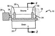
- FIG. 1is a plan view of one embodiment of a HEMT according to the present invention.
- FIG. 2is a sectional view of the HEMT in FIG. 1 ;
- FIG. 3is a plan view of another embodiment of a HEMT according to the present invention.
- FIG. 4is a sectional view of the HEMT in FIG. 3 ;
- FIG. 5is a table comparing the operating characteristics of a HEMT according to the present invention compared to a HEMT with no field plate and a HEMT with a gate connected field plate;
- FIG. 6is a chart showing the operating characteristics of a HEMT with a gate connected field plate
- FIG. 7is a chart showing the operating characteristics of a HEMT with a source connected field plate
- FIG. 8is a sectional view of a HEMT according to the present invention having a gamma shaped gate
- FIG. 9is a sectional view of a HEMT according to the present invention having a recessed gate.
- Wide bandgap transistor structuresgenerally include an active region, with metal source and drain electrodes formed in electrical contact with the active region, and a gate electrode formed between the source and drain electrodes for modulating electric fields within the active region.
- a spacer layeris formed above the active region.
- the spacer layercan comprise a dielectric layer, or a combination of multiple dielectric layers.
- a conductive field plateis formed above the spacer layer and extends a distance L f from the edge of the gate electrode toward the drain electrode.
- the field platecan be electrically connected to the source electrode.
- This field plate arrangementcan reduce the peak electric field in the device, resulting in increased breakdown voltage and reduced trapping. The reduction of the electric field can also yield other benefits such as reduced leakage currents and enhanced reliability.
- the field plate electrically connected to the source electrodeBy having the field plate electrically connected to the source electrode, the reduced gain and instability resulting from gate connected field plates is reduced.
- the shielding effect of a source-connected field platecan reduce Cgd, which enhances input-output isolation.
- One type of transistor that can utilize the field plate arrangement according to the present inventionis a high electron mobility transistor (HEMT), which typically includes a buffer layer and a barrier layer on the buffer layer.
- HEMThigh electron mobility transistor
- a two dimensional electron gas (2 DEG) layer/channelis formed at the junction between the buffer layer and the barrier layer.
- a gate electrodeis formed on the barrier layer between source and drain electrodes.
- a spacer layeris formed on the barrier layer covering at least a portion of the barrier layer between the gate and drain electrode such that a field plate can be formed on the spacer layer in electric isolation from the barrier layer.
- the spacer layercan also cover all or some of the gate such that the field plate can overlap the gate while remaining in electrical isolation from the gate and the barrier layer.
- the spacer layercovers the gate and the surface of the barrier layer between the gate and the source and drain electrodes.
- the spacer layercan comprise a dielectric layer, or a combination of multiple dielectric layers. Different dielectric materials can be used such as a SiN, SiO2, Si, Ge, MgOx, MgNx, ZnO, SiNx, SiOx, alloys or layer sequences thereof, or epitaxial materials as described below.
- a conductive field plateis formed on the spacer layer and extends a distance L f from the edge of the gate towards the drain electrode, with the field plate and gate electrode typically being formed during separate deposition steps.
- the field plateis also electrically connected to the source electrode.
- FIGS. 1 and 2show one embodiment of a nitride based HEMT 10 according to the present invention which comprises a substrate 12 of silicon carbide, sapphire, spinet, ZnO, silicon, gallium nitride, aluminum nitride, or any other material capable of supporting growth of a Group-III nitride material.
- the substrate 12can comprise semi-insulating 4H—SiC commercially available from Cree, Inc. of Durham, N.C.
- a nucleation layer 14can be formed on the substrate 12 to reduce the lattice mismatch between the substrate 12 and the next layer in the HEMT 10 .
- the nucleation layer 14should be approximately 1000 angstroms ( ⁇ ) thick, although other thicknesses can be used.
- the nucleation layer 14can be formed on the substrate 12 using known semiconductor growth techniques such as Metal Oxide Chemical Vapor Deposition (MOCVD), Hydride Vapor Phase Epitaxy (HVPE), or Molecular Beam Epitaxy (MBE).
- MOCVDMetal Oxide Chemical Vapor Deposition
- HVPEHydride Vapor Phase Epitaxy
- MBEMolecular Beam Epitaxy
- the formation of the nucleation layer 14can depend on the material used for the substrate 12 .
- methods of forming a nucleation layer 14 on various substratesare taught in U.S. Pat. Nos. 5,290,393 and 5,686,738, each of which are incorporated by reference as if fully set forth herein.
- Methods of forming nucleation layers on silicon carbide substratesare disclosed in U.S. Pat. Nos. 5,393,993, 5,523,589, and 5,739,554 each of which is incorporated herein by reference as if fully set forth herein.
- the buffer layer 16comprises a GaN layer that is approximately 2 ⁇ m thick, with part of the layer doped with Fe.
- a barrier layer 18is formed on the buffer layer 16 such that the buffer layer 16 is sandwiched between the barrier layer 18 and the nucleation layer 14 .
- Each of the buffer layer 16 and barrier layer 18can comprise doped or undoped layers of Group III-nitride materials.
- the barrier layer 18can comprise one or more layers of different materials such as InGaN, AlGaN, AlN, or combinations thereof.
- the barrier layer 18comprises 0.8 nm of AlN and 22.5 nm of Al x Ga 1-x N (x ⁇ 0.195, as measured by photo luminescence). Exemplary structures are illustrated in U.S. Pat. Nos. 6,316,793, 6,586,781, 6,548,333 and U.S. Published Patent Application Nos.
- nitride based HEMT structuresare illustrated in U.S. Pat. Nos. 5,192,987 and 5,296,395 each of which is incorporated herein by reference as if fully set forth herein.
- the buffer and barrier layers 16 , 18can be made using the same methods used to grow the nucleation layer 14 .
- a two dimensional electron gas (2 DEG) layer/channel 17is formed at the heterointerface between the buffer and barrier layer 16 , 18 . Electric isolation between the devices is achieved with mesa etch or ion implementation outside the active area of the HEMT.
- Metal source and drain electrodes 20 , 22are formed making ohmic contact through the barrier layer 18 , and a gate 24 is formed on the barrier layer 18 between the source and drain electrodes 20 , 22 .
- Electric currentcan flow between the source and drain electrodes 20 , 22 through a two-dimensional electron gas (2 DEG) 17 induced at the heterointerface between the buffer layer 16 and the barrier layer 18 when the gate 24 is biased at the appropriate level.
- 2 DEGtwo-dimensional electron gas
- the source and drain electrodes 20 , 22can be made of different materials including but not limited to alloys of titanium, aluminum, gold or nickel.
- the gate 24can also be made of different materials including but not limited to nickel, gold, platinum, titanium, chromium, alloys of titanium and tungsten, or platinum silicide.
- the gate 24can have many different lengths, with a preferred gate length (L g ) being approximately 0.5 microns. As best shown in FIG. 1 , the gate 24 is connected to and contacted at a gate electrode 28 . As described below, in other transistor embodiments according to the present invention the gate 24 can be at least partially recessed in barrier layer 18 .
- a non-conducting spacer layer 26can be formed over the gate 24 and the surface of the barrier layer 18 between the gate 24 and the source and drain electrodes 20 , 22 , although as described above the spacer layer can cover less.
- the spacer layer 26can comprise a layer of non-conducting material such as a dielectric. Alternatively, it can comprise a number of different layers of dielectrics or a combination of dielectric layers.
- the spacer layercan be many different thicknesses, with a suitable range of thicknesses being approximately 0.05 to 2 microns.
- the spacer layer 26can comprise an epitaxial material such as a Group III nitride material having different Group III elements such as alloys of Al, Ga, or In, with a suitable spacer layer material being Al x Ga 1-x N (0 ⁇ x ⁇ 1).
- the spacer layer 26can be grown using the same epitaxial growth method.
- the spacer layer 26is then etched such that the gate 24 , source electrode 20 and drain electrode 22 can be properly formed in contact with the buffer layer 18 and the 2 DEG 17 .
- a field platecan then be deposited on the spacer layer between the gate 24 and drain electrode 22 . In those embodiments where the field plate overlaps the gate, an additional spacer layer of dielectric material should be included at least partially over the gate to isolate the gate from the field plate.
- a field plate 30is formed on the spacer layer 26 between the gate 24 and the drain electrode 22 , with the field plate 30 being in close proximity to the gate 24 but not overlapping it.
- a space between the gate 24 and field plate (L gf )remains and should be wide enough to isolate from the field plate 30 , while being small enough to maximize the field effect provided by the field plate 30 . If L gf is too wide the field effect can be reduced. In one embodiment according to the present invention L gf should be approximately 0.4 microns or less, although larger and smaller spaces can also be used.
- the field plate 30can extend different distances L f from the edge of the gate 24 , with a suitable range of distances for L f being approximately 0.1 to 2 microns.
- the field plate 30can comprise many different conductive materials with a suitable material being a metal, or combinations of metals, deposited using standard metallization methods.
- the field plate 30comprises titanium/gold or nickel/gold.
- the field plate 30is electrically connected to the source electrode 20 and FIG. 1 shows two connection structures that can be used according to the present invention, although other connection structures can also be used.
- Conductive buses 32can be formed on the spacer layer 26 to extend between the field plate 30 and the source electrode 20 . Different numbers of buses 32 can be used although the greater the number of buses the greater the unwanted capacitance that can be introduced by the buses and the buses 32 should cover less than all of the all of the topmost surface between gate 24 and source electrode 20 .
- the busesshould have a sufficient number so that current effectively spreads from the source electrode 20 into the field plate 30 , while not covering too much of the HEMT's active region, with a suitable number of buses 32 being two.
- the field plate 30can alternatively be electrically connected to the source electrode 20 through a conductive path 34 that runs outside of the active regions of the HEMT 10 , the field plate and the source electrode 20 .
- the path 34runs outside the active area of the HEMT at the side opposite the gate electrode 28 .
- the conductive pathcould run outside the active area of the HEMT 10 on the side of the gate electrode 28 , or the HEMT 10 could include two or more conductive paths running out the same or different sides of the HEMT 10 .
- the active structurecan be covered by a dielectric passivation layer (not shown), such as silicon nitride.
- a dielectric passivation layersuch as silicon nitride.
- FIGS. 3 and 4show another embodiment of a HEMT 40 according to the present invention having many features that are similar to those in HEMT 10 of FIGS. 1 and 2 .
- the same reference numeralsare used and the features are introduced without full description with the understanding that the description of the features above applies equally to the HEMT 40 .
- the HEMT 40comprises a substrate 12 , nucleation layer 14 , buffer layer 16 , 2 DEG 17 , barrier layer 18 , source electrode 20 , drain electrode 22 , gate 24 , spacer layer 26 and gate electrode 28 .
- the HEMT 40also comprises a field plate 42 that is formed on the spacer layer 26 primarily between the gate 24 and the drain electrode 22 , but also overlapping a portion of the gate 24 .
- L gfis small, which can present some difficulties during fabrication.
- the field plate 42overlap the gate 24 the HEMT 40 can be fabricated without having to meet the tolerances of L gf .
- the overlapping section of the field plate 42can introduce additional unwanted capacitance. In determining whether to use a field plate 30 or 42 the ease of manufacturing using field plate 42 must be balanced with the reduced capacitance provided by field plate 30 .
- the HEMT 40also comprises either buses 44 or a conductive path 46 to electrically connect the field plate 42 to the source electrode 20 .
- the active structurecan also be covered by a dielectric passivation layer (not shown), such as silicon nitride.
- FIG. 5shows a table 50 comparing the operating characteristics of GaN based HEMTs with no field plate to HEMTs having a field plate connected to the gate, and field plate connected to the source.
- HEMTs with source connected field platesexhibit improved maximum stable gain (MSG) and reduced reverse power transmission (S 12 ).
- MSGmaximum stable gain
- S 12 of a HEMT with a gate connected field plateis increased by 71% at 4 GHz, while that of the device with a source connected field plate is actually reduced by 28%.
- FIG. 6is a graph 60 showing the performance of a gate connected field plate device
- FIG. 7is a graph 70 showing the performance of a source connected field plate device.
- Both field plate deviceswere able to operate at 118 V dc bias wherein tuning was optimized for the best combination of gain, PAE and output power at 3 dB compression (P 3 dB ). While both devices generate power densities of approximately 20 W/mm, the source connected field plate device provides a 7 dB higher associated gain. With the achieved large-signal gain of 21 dB at 4 GHz and the estimated voltage swing of 224V, the voltage-frequency-gain product approaches 10 kV-GHz.
- FIG. 8shows another embodiment of a HEMT 80 according to the present invention that has many features similar to those in HEMTs 10 and 40 , including a substrate 12 , nucleation layer 14 , buffer layer 16 , 2 DEG 17 , barrier layer 18 , source electrode 20 , and drain electrode 22 .
- HEMT 80has a gamma ( ⁇ ) shaped gate 82 that is particularly adapted to high frequency operation.
- the gate length (L g )is one of the important device dimensions in determining the speed of the device, and with higher frequency devices the gate length is shorter. Shorter gate length can lead to high resistance that can negatively impact high frequency operation.
- T-gatesare commonly used in high frequency operation, but it can be difficult to achieve a well-coupled placement of a field plate with a T-gate.
- the gamma gate 82provides for low gate resistance and allows for controlled definition of the gate footprint.
- a spacer layer 84is included that covers the gamma gate 82 and the surface of barrier layer 18 between the gamma gate 82 and the source and drain electrodes 20 , 22 .
- a spacecan remain between the horizontal portion of the gamma gate 82 and the top of the spacer layer 84 .
- the HEMT 80also includes a field plate 86 on the spacer layer 84 that overlaps that gamma gate 82 , with the field plate 86 preferably deposited on the side of the gamma gate 82 not having a horizontal overhanging section. This arrangement allows for tight placement and effective coupling between the field plate 86 and the active layers below it.
- the field platecan be similarly arranged to field plate 86 , but instead of overlapping the gate, there can be a space between the edge of the gate and the field plate similar to space Lgf shown in FIG. 2 .
- the field plate 86can be electrically connected to the source electrode 20 in many different ways. Because of the space between the lower surface of the horizontal section of the gate 82 and the spacer layer 84 , it can be difficult to provide a conductive path directly between the field plate 86 and the source electrode 20 . Instead, conductive path can be included between the field plate 86 and the source electrode 20 that runs outside the active area of the HEMT 80 . Alternatively, the gamma gate 82 can be completely covered by the spacer layer 84 with the space under the gate's horizontal section filled. Conductive paths can then run directly from the field plate 86 to the source electrode over the spacer layer 84 . The active structure can then be covered by a dielectric passivation layer (not shown).
- FIG. 9shows still another HEMT 90 according to the present invention that can also be arranged with a source connected field plate.
- HEMT 90also has many features similar to those in HEMTs 10 and 40 in FIGS. 1-4 , including a substrate 12 , nucleation layer 14 , buffer layer 16 , 2 DEG 17 , barrier layer 18 , source electrode 20 , and drain electrode 22 .
- the gate 92is recessed in the barrier layer 18 , and is covered by a spacer layer 94 . In other embodiments the bottom surface of the gate can be only partially recessed or different portions of the gate can be recessed to different depths in the barrier layer 18 .
- a field plate 96is arranged on the spacer layer 94 and is electrically connected to the source electrode 20 and the active structure can be covered by a dielectric passivation layer (not shown).
- the embodiments aboveprovide wide bandgap transistors, particularly HEMTs, with improved power at microwave and millimeter wave frequencies.
- the HEMTsexhibit simultaneous high gain, high power, and more stable operation due to higher input-output isolation.
- the structurecould be extended to larger dimensions for high voltage applications at lower frequencies.
Landscapes
- Junction Field-Effect Transistors (AREA)
- Electrodes Of Semiconductors (AREA)
Abstract
Description
This application is a divisional of and claims the benefit of U.S. patent application Ser. No. 10/958,970 filed on Oct. 4, 2004 now U.S. Pat. No. 7,550,783, which claims the benefit of U.S. Provisional patent application Ser. No. 60/570,519 filed May 11, 2004.
This invention was made with Government support under ONR/DARPA Government Contract No. N00014-02-0306. The Government has certain rights in this invention.
1. Field of the Invention
The present invention relates to transistors and particularly to transistors utilizing field plates.
2. Description of the Related Art
Improvements in the manufacturing of AlGaN/GaN semiconductor materials have helped advance the development of AlGaN/GaN transistors, such as high electron mobility transistors (HEMTs) for high frequency, high temperature and high power applications. AlGaN/GaN has large bandgaps, high peak and saturation electron velocity values [B. Gelmont, K. Kim and M. Shur,Monte Carlo Simulation of Electron Transport in Gallium Nitride, J. Appl. Phys. 74, (1993), pp. 1818-1821]. AlGaN/GaN HEMTs can also have 2 DEG sheet densities in excess of 1013cm−2and relatively high electron mobility (up to 2019 cm2/Vs) [R. Gaska, et al.,Electron Transport in AlGaN—GaN Heterostructures Grown on6H—SiC Substrates, Appl. Phys. Lett. 72, (1998), pp. 707-709]. These characteristics allow AlGaN/GaN HEMTs to provide very high voltage and high power operation at RF, microwave and millimeter wave frequencies.
AlGaN/GaN HEMTs have been grown on sapphire substrates and have shown a power density of 4.6 W/mm and a total power of 7.6 W [Y. F. Wu et al.,GaN-Based FETs for Microwave Power Amplification, IEICE Trans. Electron. E-82-C, (1999). pp. 1895-1905]. More recently, AlGaN/GaN HEMTs grown on SiC have shown a power density of 9.8 W/mm at 8 GHz [Y. F. Wu, et al.,Very-High Power Density AlGaN/GaN HEMTs, IEEE Trans. Electron. Dev. 48, (2001), pp. 586-590] and a total output power of 22.9 W at 9 GHz [M. Micovic, et al.,AlGaN/GaN Heterojunction Field Effect Transistors Grown by Nitrogen Plasma Assisted Molecular Beam Epitaxy, IEEE Trans. Electron. Dev. 48, (2001), pp. 591-596].
U.S. Pat. No. 5,192,987 to Khan et al. discloses GaN/AlGaN based HEMTs grown on a buffer and a substrate. Other AlGaN/GaN HEMTs and field effect transistors (FETs) have been described by Gaska et al.,High-Temperature Performance of AlGaN/GaN HFET's on SiC Substrates, IEEE Electron Device Letters, 18, (1997), pp. 492-494; and Ping et al.,DC and Microwave Performance of High Current AlGaN Heterostructure Field Effect Transistors Grown on P-type SiC Substrates, IEEE Electron Devices Letters 19, (1998), pp. 54-56. Some of these devices have shown a gain-bandwidth product (fT) as high as 67 gigahertz [K. Chu et al. WOCSEMMAD, Monterey, Calif. (February 1998)] and high power densities up to 2.84 W/mm at 10 GHz [G. Sullivan et al.,High Power10-GHz Operation of AlGaN HFET's in Insulating SiC, IEEE Electron Device Letters 19, (1998), pp. 198-200; and Wu et al.,High Al-Content AlGaN/GaN MODFETs for Ultrahigh Performance, IEEE Electron Device Letters 19, (1998), pp. 50-53].
Electron trapping and the resulting difference between DC and RF characteristics have been a limiting factor in the performance of these devices. Silicon nitride (SiN) passivation has been successfully employed to alleviate this trapping problem resulting in high performance devices with power densities over 10 W/mm at 10 Ghz. For example, U.S. Pat. No. 6,586,781, which is incorporated herein by reference in its entirety, discloses methods and structures for reducing the trapping effect in GaN-based transistors. However, due to the high electric fields existing in these structures, charge trapping is still an issue.
Field plates (FP) have been used to enhance the performance of GaN-based HEMTs at microwave frequencies [See S Kamalkar and U. K. Mishra,Very High Voltage AlGaN/GaN High Electron Mobility Transistors Using a Field Plate Deposited on a Stepped Insulator, Solid State Electronics 45, (2001), pp. 1645-1662]. These approaches, however, have involved a field plate connected to the gate of the transistor with the field plate on top of the drain side of the channel. This can result in a significant FP-to-drain capacitance and the field plate being connected to the gate adds additional gate-to-drain capacitance (Cgd) to the device. This can not only reduce gain, but can also cause instability due to poorer input-output isolation.
The present invention provides transistors with a field plate connected to the source electrode, with typical transistors utilizing the invention being HEMTs. One embodiment of a HEMT according to the present invention comprises a plurality of active semiconductor layers formed on a substrate with a two dimensional electron gas (2 DEG) at the heterointerface between two of said plurality of active layers. Source and drain electrodes are formed in contact with the 2 DEG and a gate is formed between the source and drain electrodes and on the plurality of active layers. A spacer layer is formed on at least part of the surface of the plurality of active layers between the gate and the drain electrode. A field plate is formed on the spacer layer with at least one conductive path electrically connecting the field plate to the source electrode, the at least one conductive path covering less than all of the topmost surface between gate and source electrode.
Another embodiment of a HEMT according to the present invention comprises a buffer layer and barrier layer formed successively on a substrate and a two dimensional electron gas (2 DEG) at the heterointerface between the buffer and barrier layers. A source and a drain electrode are included both making ohmic contact with the 2 DEG and a gate is included on the barrier layer between the source and drain electrodes. A spacer layer covers at least a portion of the barrier layer between the gate and drain electrode. A field plate is included on the spacer layer isolated from the barrier layer and extending a distance Lffrom the gate toward the drain electrode. The field plate is electrically connected to the source electrode by at least one conductive path that covers less than all of the topmost layer between the gate and source electrode.
Still another embodiment of a HEMT according to the present invention comprises a plurality of active semiconductor layers formed on a substrate and a two dimensional electron gas (2 DEG) at the heterointerface between two of the plurality of active layers. Source and drain electrodes are included in contact with the 2 DEG. A gate is included between the source and drain electrodes and on the plurality of active layers. A field plate extends a distance Lffrom the edge of the gate to the drain electrode, with the field plate isolated from the gate electrode and active layers. At least one conductive path electrically connects the field plate to the source electrode, with the at least one conductive path covering less than all of the topmost surface between gate and source electrode.
These and other further features and advantages of the invention would be apparent to those skilled in the art from the following detailed description, taking together with the accompanying drawings, in which:
The field plate arrangements according to the present invention can be used with many different transistor structures. Wide bandgap transistor structures generally include an active region, with metal source and drain electrodes formed in electrical contact with the active region, and a gate electrode formed between the source and drain electrodes for modulating electric fields within the active region. A spacer layer is formed above the active region. The spacer layer can comprise a dielectric layer, or a combination of multiple dielectric layers. A conductive field plate is formed above the spacer layer and extends a distance Lffrom the edge of the gate electrode toward the drain electrode.
The field plate can be electrically connected to the source electrode. This field plate arrangement can reduce the peak electric field in the device, resulting in increased breakdown voltage and reduced trapping. The reduction of the electric field can also yield other benefits such as reduced leakage currents and enhanced reliability. By having the field plate electrically connected to the source electrode, the reduced gain and instability resulting from gate connected field plates is reduced. When arranged according to the present invention, the shielding effect of a source-connected field plate can reduce Cgd, which enhances input-output isolation.
One type of transistor that can utilize the field plate arrangement according to the present invention is a high electron mobility transistor (HEMT), which typically includes a buffer layer and a barrier layer on the buffer layer. A two dimensional electron gas (2 DEG) layer/channel is formed at the junction between the buffer layer and the barrier layer. A gate electrode is formed on the barrier layer between source and drain electrodes.
According to the present invention, a spacer layer is formed on the barrier layer covering at least a portion of the barrier layer between the gate and drain electrode such that a field plate can be formed on the spacer layer in electric isolation from the barrier layer. In other embodiments the spacer layer can also cover all or some of the gate such that the field plate can overlap the gate while remaining in electrical isolation from the gate and the barrier layer. In a preferred embodiment the spacer layer covers the gate and the surface of the barrier layer between the gate and the source and drain electrodes. The spacer layer can comprise a dielectric layer, or a combination of multiple dielectric layers. Different dielectric materials can be used such as a SiN, SiO2, Si, Ge, MgOx, MgNx, ZnO, SiNx, SiOx, alloys or layer sequences thereof, or epitaxial materials as described below.
A conductive field plate is formed on the spacer layer and extends a distance Lffrom the edge of the gate towards the drain electrode, with the field plate and gate electrode typically being formed during separate deposition steps. The field plate is also electrically connected to the source electrode.
It will be understood that when an element or layer is referred to as being “on”, “connected to”, “coupled to” or “in contact with” another element or layer, it can be directly on, connected or coupled to, or in contact with the other element or layer or intervening elements or layers may be present. In contrast, when an element is referred to as being “directly on,” “directly connected to”, “directly coupled to” or “directly in contact with” another element or layer, there are no intervening elements or layers present. Likewise, when a first element or layer is referred to as being “in electrical contact with” or “electrically coupled to” a second element or layer, there is an electrical path that permits current flow between the first element or layer and the second element or layer. The electrical path may include capacitors, coupled inductors, and/or other elements that permit current flow even without direct contact between conductive elements.
Anucleation layer 14 can be formed on thesubstrate 12 to reduce the lattice mismatch between thesubstrate 12 and the next layer in theHEMT 10. Thenucleation layer 14 should be approximately 1000 angstroms (Å) thick, although other thicknesses can be used. Thenucleation layer 14 can comprise many different materials, with a suitable material being AlzGa1-zN (0<=z<=1). Thenucleation layer 14 can be formed on thesubstrate 12 using known semiconductor growth techniques such as Metal Oxide Chemical Vapor Deposition (MOCVD), Hydride Vapor Phase Epitaxy (HVPE), or Molecular Beam Epitaxy (MBE).
The formation of thenucleation layer 14 can depend on the material used for thesubstrate 12. For example, methods of forming anucleation layer 14 on various substrates are taught in U.S. Pat. Nos. 5,290,393 and 5,686,738, each of which are incorporated by reference as if fully set forth herein. Methods of forming nucleation layers on silicon carbide substrates are disclosed in U.S. Pat. Nos. 5,393,993, 5,523,589, and 5,739,554 each of which is incorporated herein by reference as if fully set forth herein.
TheHEMT 10 further comprises a highresistivity buffer layer 16 formed on thenucleation layer 14, with asuitable buffer layer 16 made of a Group III-nitride material such as AlxGayIn(1-x-y)N (0<=x<=1, 0<=y<=1, x+y<=1). In another embodiment according to the present invention thebuffer layer 16 comprises a GaN layer that is approximately 2 μm thick, with part of the layer doped with Fe.
Abarrier layer 18 is formed on thebuffer layer 16 such that thebuffer layer 16 is sandwiched between thebarrier layer 18 and thenucleation layer 14. Each of thebuffer layer 16 andbarrier layer 18 can comprise doped or undoped layers of Group III-nitride materials. Thebarrier layer 18 can comprise one or more layers of different materials such as InGaN, AlGaN, AlN, or combinations thereof. In one embodiment thebarrier layer 18 comprises 0.8 nm of AlN and 22.5 nm of AlxGa1-xN (x≈0.195, as measured by photo luminescence). Exemplary structures are illustrated in U.S. Pat. Nos. 6,316,793, 6,586,781, 6,548,333 and U.S. Published Patent Application Nos. 2002/0167023 and 2003/00020092 each of which is incorporated by reference as though fully set forth herein. Other nitride based HEMT structures are illustrated in U.S. Pat. Nos. 5,192,987 and 5,296,395 each of which is incorporated herein by reference as if fully set forth herein. The buffer and barrier layers16,18 can be made using the same methods used to grow thenucleation layer 14. A two dimensional electron gas (2 DEG) layer/channel 17 is formed at the heterointerface between the buffer andbarrier layer
Metal source and drainelectrodes barrier layer 18, and agate 24 is formed on thebarrier layer 18 between the source and drainelectrodes electrodes buffer layer 16 and thebarrier layer 18 when thegate 24 is biased at the appropriate level. The formation of source and drainohmic contacts
The source and drainelectrodes gate 24 can also be made of different materials including but not limited to nickel, gold, platinum, titanium, chromium, alloys of titanium and tungsten, or platinum silicide. Thegate 24 can have many different lengths, with a preferred gate length (Lg) being approximately 0.5 microns. As best shown inFIG. 1 , thegate 24 is connected to and contacted at agate electrode 28. As described below, in other transistor embodiments according to the present invention thegate 24 can be at least partially recessed inbarrier layer 18.
Anon-conducting spacer layer 26 can be formed over thegate 24 and the surface of thebarrier layer 18 between thegate 24 and the source and drainelectrodes spacer layer 26 can comprise a layer of non-conducting material such as a dielectric. Alternatively, it can comprise a number of different layers of dielectrics or a combination of dielectric layers. The spacer layer can be many different thicknesses, with a suitable range of thicknesses being approximately 0.05 to 2 microns.
When thespacer layer 26 is formed before device metallization thespacer layer 26 can comprise an epitaxial material such as a Group III nitride material having different Group III elements such as alloys of Al, Ga, or In, with a suitable spacer layer material being AlxGa1-xN (0<x<1). After epitaxial growth of thebarrier layer 18, thespacer layer 26 can be grown using the same epitaxial growth method. Thespacer layer 26 is then etched such that thegate 24,source electrode 20 anddrain electrode 22 can be properly formed in contact with thebuffer layer 18 and the 2DEG 17. A field plate can then be deposited on the spacer layer between thegate 24 anddrain electrode 22. In those embodiments where the field plate overlaps the gate, an additional spacer layer of dielectric material should be included at least partially over the gate to isolate the gate from the field plate.
Afield plate 30 is formed on thespacer layer 26 between thegate 24 and thedrain electrode 22, with thefield plate 30 being in close proximity to thegate 24 but not overlapping it. A space between thegate 24 and field plate (Lgf) remains and should be wide enough to isolate from thefield plate 30, while being small enough to maximize the field effect provided by thefield plate 30. If Lgfis too wide the field effect can be reduced. In one embodiment according to the present invention Lgfshould be approximately 0.4 microns or less, although larger and smaller spaces can also be used.
Thefield plate 30 can extend different distances Lffrom the edge of thegate 24, with a suitable range of distances for Lfbeing approximately 0.1 to 2 microns. Thefield plate 30 can comprise many different conductive materials with a suitable material being a metal, or combinations of metals, deposited using standard metallization methods. In one embodiment according to the present invention thefield plate 30 comprises titanium/gold or nickel/gold.
Thefield plate 30 is electrically connected to thesource electrode 20 andFIG. 1 shows two connection structures that can be used according to the present invention, although other connection structures can also be used.Conductive buses 32 can be formed on thespacer layer 26 to extend between thefield plate 30 and thesource electrode 20. Different numbers ofbuses 32 can be used although the greater the number of buses the greater the unwanted capacitance that can be introduced by the buses and thebuses 32 should cover less than all of the all of the topmost surface betweengate 24 andsource electrode 20. The buses should have a sufficient number so that current effectively spreads from thesource electrode 20 into thefield plate 30, while not covering too much of the HEMT's active region, with a suitable number ofbuses 32 being two.
Thefield plate 30 can alternatively be electrically connected to thesource electrode 20 through aconductive path 34 that runs outside of the active regions of theHEMT 10, the field plate and thesource electrode 20. As shown inFIG. 1 , thepath 34 runs outside the active area of the HEMT at the side opposite thegate electrode 28. In alternative embodiments according to the present invention, the conductive path could run outside the active area of theHEMT 10 on the side of thegate electrode 28, or theHEMT 10 could include two or more conductive paths running out the same or different sides of theHEMT 10.
After deposition of thefield plate 30 and its connection to thesource electrode 20, the active structure can be covered by a dielectric passivation layer (not shown), such as silicon nitride. Methods of forming the dielectric passivation layer are described in detail in the patents and publications referenced above.
TheHEMT 40 comprises asubstrate 12,nucleation layer 14,buffer layer DEG 17,barrier layer 18,source electrode 20,drain electrode 22,gate 24,spacer layer 26 andgate electrode 28. TheHEMT 40 also comprises afield plate 42 that is formed on thespacer layer 26 primarily between thegate 24 and thedrain electrode 22, but also overlapping a portion of thegate 24. For theHEMT 10 inFIGS. 1 and 2 , Lgfis small, which can present some difficulties during fabrication. By having thefield plate 42 overlap thegate 24 theHEMT 40 can be fabricated without having to meet the tolerances of Lgf. The overlapping section of thefield plate 42, however, can introduce additional unwanted capacitance. In determining whether to use afield plate field plate 42 must be balanced with the reduced capacitance provided byfield plate 30.
TheHEMT 40 also comprises eitherbuses 44 or aconductive path 46 to electrically connect thefield plate 42 to thesource electrode 20. After deposition of thefield plate 42 and its connection to thesource electrode 20, the active structure can also be covered by a dielectric passivation layer (not shown), such as silicon nitride.
The source connected field plate arrangement according to the present invention can be used in many different HEMTs beyond those described above. For example,FIG. 8 shows another embodiment of aHEMT 80 according to the present invention that has many features similar to those inHEMTs substrate 12,nucleation layer 14,buffer layer DEG 17,barrier layer 18,source electrode 20, and drainelectrode 22.HEMT 80, however, has a gamma (Γ) shapedgate 82 that is particularly adapted to high frequency operation. The gate length (Lg) is one of the important device dimensions in determining the speed of the device, and with higher frequency devices the gate length is shorter. Shorter gate length can lead to high resistance that can negatively impact high frequency operation. T-gates are commonly used in high frequency operation, but it can be difficult to achieve a well-coupled placement of a field plate with a T-gate.
Thegamma gate 82 provides for low gate resistance and allows for controlled definition of the gate footprint. Aspacer layer 84 is included that covers thegamma gate 82 and the surface ofbarrier layer 18 between thegamma gate 82 and the source and drainelectrodes gamma gate 82 and the top of thespacer layer 84. TheHEMT 80 also includes afield plate 86 on thespacer layer 84 that overlaps thatgamma gate 82, with thefield plate 86 preferably deposited on the side of thegamma gate 82 not having a horizontal overhanging section. This arrangement allows for tight placement and effective coupling between thefield plate 86 and the active layers below it. In other gamma gate embodiments the field plate can be similarly arranged tofield plate 86, but instead of overlapping the gate, there can be a space between the edge of the gate and the field plate similar to space Lgf shown inFIG. 2 .
Thefield plate 86 can be electrically connected to thesource electrode 20 in many different ways. Because of the space between the lower surface of the horizontal section of thegate 82 and thespacer layer 84, it can be difficult to provide a conductive path directly between thefield plate 86 and thesource electrode 20. Instead, conductive path can be included between thefield plate 86 and thesource electrode 20 that runs outside the active area of theHEMT 80. Alternatively, thegamma gate 82 can be completely covered by thespacer layer 84 with the space under the gate's horizontal section filled. Conductive paths can then run directly from thefield plate 86 to the source electrode over thespacer layer 84. The active structure can then be covered by a dielectric passivation layer (not shown).
The embodiments above provide wide bandgap transistors, particularly HEMTs, with improved power at microwave and millimeter wave frequencies. The HEMTs exhibit simultaneous high gain, high power, and more stable operation due to higher input-output isolation. The structure could be extended to larger dimensions for high voltage applications at lower frequencies.
Although the present invention has been described in considerable detail with reference to certain preferred configurations thereof, other versions are possible. The field plate arrangement can be used in many different devices. The field plates can also have many different shapes and can be connected to the source electrode in many different ways. The spirit and scope of the invention should not be limited to the preferred versions of the invention described above.
Claims (21)
1. A transistor, comprising:
a plurality of semiconductor layers;
source and drain electrodes on said semiconductor layers;
a gate between said source and drain electrodes and on said semiconductor layers;
a spacer layer covering at least part of a surface of the semiconductor layers between said gate and said drain, or covering at least part of the surface of said semiconductor layers between said gate and said source;
a field plate on said spacer layer; and
a conductive path running outside an area covered by said semiconductor layers, and between said field plate and said source electrode to electrically connect said field plate to said source electrode.
2. The transistor ofclaim 1 , further comprising a gate electrode, wherein said conductive path runs outside of said semiconductor layers at a side opposite said gate electrode.
3. The transistor ofclaim 1 , further comprising a gate electrode, wherein said conductive path runs outside of said semiconductor layers on the same side as said gate electrode.
4. The transistor ofclaim 1 , further comprising a second conductive path electrically connecting said field plate to said source electrode and running outside of the area covered by said semiconductor layers on a side opposite said conductive path.
5. The transistor ofclaim 1 , wherein said field plate extends on said spacer layer from an edge of said gate toward said drain electrode.
6. The transistor ofclaim 1 , wherein said spacer layer at least partially covers said gate and said field plate at least partially overlaps said gate and extends on said spacer layer from an edge of said gate toward said drain electrode.
7. The transistor ofclaim 1 , wherein said semiconductor layers are gallium nitride based.
8. The transistor ofclaim 1 , wherein said spacer layer comprises a dielectric material.
9. The transistor ofclaim 1 , wherein said gate is gamma shaped.
10. The transistor ofclaim 1 , wherein said gate is at least partially recessed in one of said semiconductor layers.
11. The transistor ofclaim 1 , wherein said field plate reduces the peak operating electric field.
12. The transistor ofclaim 11 , wherein said reduction in peak operating electric field increases the breakdown voltage.
13. The transistor ofclaim 11 , wherein said reduction in peak operating electric field reduces trapping.
14. The transistor ofclaim 11 , wherein said reduction in peak operating electric field reduces leakage current.
15. A transistor, comprising:
a barrier layer on a buffer layer;
source and drain electrodes on said barrier layer;
a gate on said barrier layer and between said source and drain electrodes;
a spacer layer covering at least a portion of said buffer layer between said gate and said source, and at least a portion of said barrier layer between said gate and drain electrode; and
a field plate formed on said spacer layer isolated from the barrier layer and extending a distance Lf from said gate toward said drain electrode, said field plate electrically connected to said source electrode by at least one conductive structure, whereby a surface between said gate and said source electrode is not covered by said conductive structure.
16. The transistor ofclaim 15 , wherein said at least one conductive structure comprising one or more conductive paths running outside of an area covered by said buffer layer and between said field plate and said source electrode.
17. The transistor ofclaim 15 , said spacer layer providing electrical isolation between said buffer layer and said field plate.
18. The transistor ofclaim 15 , wherein said spacer layer comprises a dielectric material.
19. The transistor ofclaim 15 , further comprising a substrate wherein said buffer and barrier layer are on said substrate.
20. The transistor ofclaim 15 , covered by a passivation layer.
21. The transistor ofclaim 15 , wherein said field plate reduces the peak operating electric field in said HEMT.
Priority Applications (2)
| Application Number | Priority Date | Filing Date | Title |
|---|---|---|---|
| US12/437,505US7915644B2 (en) | 2004-05-11 | 2009-05-07 | Wide bandgap HEMTs with source connected field plates |
| US13/072,449US8592867B2 (en) | 2004-05-11 | 2011-03-25 | Wide bandgap HEMTS with source connected field plates |
Applications Claiming Priority (3)
| Application Number | Priority Date | Filing Date | Title |
|---|---|---|---|
| US57051904P | 2004-05-11 | 2004-05-11 | |
| US10/958,970US7550783B2 (en) | 2004-05-11 | 2004-10-04 | Wide bandgap HEMTs with source connected field plates |
| US12/437,505US7915644B2 (en) | 2004-05-11 | 2009-05-07 | Wide bandgap HEMTs with source connected field plates |
Related Parent Applications (1)
| Application Number | Title | Priority Date | Filing Date |
|---|---|---|---|
| US10/958,970DivisionUS7550783B2 (en) | 2004-05-11 | 2004-10-04 | Wide bandgap HEMTs with source connected field plates |
Related Child Applications (1)
| Application Number | Title | Priority Date | Filing Date |
|---|---|---|---|
| US13/072,449ContinuationUS8592867B2 (en) | 2004-05-11 | 2011-03-25 | Wide bandgap HEMTS with source connected field plates |
Publications (2)
| Publication Number | Publication Date |
|---|---|
| US20090236635A1 US20090236635A1 (en) | 2009-09-24 |
| US7915644B2true US7915644B2 (en) | 2011-03-29 |
Family
ID=34964651
Family Applications (3)
| Application Number | Title | Priority Date | Filing Date |
|---|---|---|---|
| US10/958,970Expired - LifetimeUS7550783B2 (en) | 2004-05-11 | 2004-10-04 | Wide bandgap HEMTs with source connected field plates |
| US12/437,505Expired - LifetimeUS7915644B2 (en) | 2004-05-11 | 2009-05-07 | Wide bandgap HEMTs with source connected field plates |
| US13/072,449Expired - LifetimeUS8592867B2 (en) | 2004-05-11 | 2011-03-25 | Wide bandgap HEMTS with source connected field plates |
Family Applications Before (1)
| Application Number | Title | Priority Date | Filing Date |
|---|---|---|---|
| US10/958,970Expired - LifetimeUS7550783B2 (en) | 2004-05-11 | 2004-10-04 | Wide bandgap HEMTs with source connected field plates |
Family Applications After (1)
| Application Number | Title | Priority Date | Filing Date |
|---|---|---|---|
| US13/072,449Expired - LifetimeUS8592867B2 (en) | 2004-05-11 | 2011-03-25 | Wide bandgap HEMTS with source connected field plates |
Country Status (8)
| Country | Link |
|---|---|
| US (3) | US7550783B2 (en) |
| EP (4) | EP2270871B1 (en) |
| JP (3) | JP5390768B2 (en) |
| KR (1) | KR101101671B1 (en) |
| CN (1) | CN100580954C (en) |
| CA (1) | CA2566756C (en) |
| TW (2) | TWI397998B (en) |
| WO (1) | WO2005114744A2 (en) |
Cited By (38)
| Publication number | Priority date | Publication date | Assignee | Title |
|---|---|---|---|---|
| US20090072269A1 (en)* | 2007-09-17 | 2009-03-19 | Chang Soo Suh | Gallium nitride diodes and integrated components |
| US20090267078A1 (en)* | 2008-04-23 | 2009-10-29 | Transphorm Inc. | Enhancement Mode III-N HEMTs |
| US20100073067A1 (en)* | 2008-09-23 | 2010-03-25 | Transphorm Inc. | Inductive Load Power Switching Circuits |
| US20100289067A1 (en)* | 2009-05-14 | 2010-11-18 | Transphorm Inc. | High Voltage III-Nitride Semiconductor Devices |
| US20110049526A1 (en)* | 2009-08-28 | 2011-03-03 | Transphorm Inc. | Semiconductor Devices with Field Plates |
| US20110095336A1 (en)* | 2009-10-26 | 2011-04-28 | Infineon Technologies Austria Ag | Lateral hemt and method for the production of a lateral hemt |
| US20110127541A1 (en)* | 2008-12-10 | 2011-06-02 | Transphorm Inc. | Semiconductor heterostructure diodes |
| US20110140172A1 (en)* | 2009-12-10 | 2011-06-16 | Transphorm Inc. | Reverse side engineered iii-nitride devices |
| US20110169054A1 (en)* | 2004-05-11 | 2011-07-14 | Cree, Inc. | Wide bandgap hemts with source connected field plates |
| US20130228789A1 (en)* | 2012-03-02 | 2013-09-05 | Kabushiki Kaisha Toshiba | Semiconductor device |
| US20130228788A1 (en)* | 2012-03-01 | 2013-09-05 | Kabushiki Kaisha Toshiba | Semiconductor device |
| US8598937B2 (en) | 2011-10-07 | 2013-12-03 | Transphorm Inc. | High power semiconductor electronic components with increased reliability |
| US8643062B2 (en) | 2011-02-02 | 2014-02-04 | Transphorm Inc. | III-N device structures and methods |
| US8716141B2 (en) | 2011-03-04 | 2014-05-06 | Transphorm Inc. | Electrode configurations for semiconductor devices |
| US8742460B2 (en) | 2010-12-15 | 2014-06-03 | Transphorm Inc. | Transistors with isolation regions |
| US8772842B2 (en) | 2011-03-04 | 2014-07-08 | Transphorm, Inc. | Semiconductor diodes with low reverse bias currents |
| US8901604B2 (en) | 2011-09-06 | 2014-12-02 | Transphorm Inc. | Semiconductor devices with guard rings |
| US20150056765A1 (en)* | 2011-09-09 | 2015-02-26 | Renesas Electronics Corporation | Semiconductor device and method of manufacturing the same |
| US9093366B2 (en) | 2012-04-09 | 2015-07-28 | Transphorm Inc. | N-polar III-nitride transistors |
| US9165766B2 (en) | 2012-02-03 | 2015-10-20 | Transphorm Inc. | Buffer layer structures suited for III-nitride devices with foreign substrates |
| US9171730B2 (en) | 2013-02-15 | 2015-10-27 | Transphorm Inc. | Electrodes for semiconductor devices and methods of forming the same |
| US9184275B2 (en) | 2012-06-27 | 2015-11-10 | Transphorm Inc. | Semiconductor devices with integrated hole collectors |
| US9245992B2 (en) | 2013-03-15 | 2016-01-26 | Transphorm Inc. | Carbon doping semiconductor devices |
| US9257547B2 (en) | 2011-09-13 | 2016-02-09 | Transphorm Inc. | III-N device structures having a non-insulating substrate |
| US9306012B2 (en)* | 2013-03-15 | 2016-04-05 | Taiwan Semiconductor Manufacturing Company Limited | Strip-ground field plate |
| US9318593B2 (en) | 2014-07-21 | 2016-04-19 | Transphorm Inc. | Forming enhancement mode III-nitride devices |
| US9443941B2 (en) | 2012-06-04 | 2016-09-13 | Infineon Technologies Austria Ag | Compound semiconductor transistor with self aligned gate |
| US9443938B2 (en) | 2013-07-19 | 2016-09-13 | Transphorm Inc. | III-nitride transistor including a p-type depleting layer |
| US9536967B2 (en) | 2014-12-16 | 2017-01-03 | Transphorm Inc. | Recessed ohmic contacts in a III-N device |
| US9536966B2 (en) | 2014-12-16 | 2017-01-03 | Transphorm Inc. | Gate structures for III-N devices |
| US9590060B2 (en) | 2013-03-13 | 2017-03-07 | Transphorm Inc. | Enhancement-mode III-nitride devices |
| US9647075B2 (en) | 2015-09-16 | 2017-05-09 | Nxp Usa, Inc. | Segmented field plate structure |
| US9905658B2 (en) | 2013-11-26 | 2018-02-27 | Nxp Usa, Inc. | Transistors with field plates resistant to field plate material migration and methods of their fabrication |
| US10224401B2 (en) | 2016-05-31 | 2019-03-05 | Transphorm Inc. | III-nitride devices including a graded depleting layer |
| WO2019060046A1 (en) | 2017-09-25 | 2019-03-28 | Raytheon Company | Electrode structure for field effect transistor |
| WO2019083706A1 (en) | 2017-10-24 | 2019-05-02 | Raytheon Company | Transistor having low capacitance field plate structure |
| US11322599B2 (en) | 2016-01-15 | 2022-05-03 | Transphorm Technology, Inc. | Enhancement mode III-nitride devices having an Al1-xSixO gate insulator |
| US12446285B2 (en) | 2020-04-28 | 2025-10-14 | Infineon Technologies Ag | Group III nitride-based transistor device |
Families Citing this family (110)
| Publication number | Priority date | Publication date | Assignee | Title |
|---|---|---|---|---|
| US7230284B2 (en) | 2001-07-24 | 2007-06-12 | Cree, Inc. | Insulating gate AlGaN/GaN HEMT |
| KR100514379B1 (en)* | 2002-07-23 | 2005-09-13 | 김용철 | Apple wine production process |
| US7501669B2 (en) | 2003-09-09 | 2009-03-10 | Cree, Inc. | Wide bandgap transistor devices with field plates |
| US7573078B2 (en)* | 2004-05-11 | 2009-08-11 | Cree, Inc. | Wide bandgap transistors with multiple field plates |
| US9773877B2 (en)* | 2004-05-13 | 2017-09-26 | Cree, Inc. | Wide bandgap field effect transistors with source connected field plates |
| JP4744109B2 (en)* | 2004-07-20 | 2011-08-10 | トヨタ自動車株式会社 | Semiconductor device and manufacturing method thereof |
| US20060073621A1 (en)* | 2004-10-01 | 2006-04-06 | Palo Alto Research Center Incorporated | Group III-nitride based HEMT device with insulating GaN/AlGaN buffer layer |
| US11791385B2 (en)* | 2005-03-11 | 2023-10-17 | Wolfspeed, Inc. | Wide bandgap transistors with gate-source field plates |
| US20060226442A1 (en)* | 2005-04-07 | 2006-10-12 | An-Ping Zhang | GaN-based high electron mobility transistor and method for making the same |
| US7855401B2 (en) | 2005-06-29 | 2010-12-21 | Cree, Inc. | Passivation of wide band-gap based semiconductor devices with hydrogen-free sputtered nitrides |
| US7525122B2 (en)* | 2005-06-29 | 2009-04-28 | Cree, Inc. | Passivation of wide band-gap based semiconductor devices with hydrogen-free sputtered nitrides |
| US7598576B2 (en)* | 2005-06-29 | 2009-10-06 | Cree, Inc. | Environmentally robust passivation structures for high-voltage silicon carbide semiconductor devices |
| EP1938385B1 (en)* | 2005-09-07 | 2014-12-03 | Cree, Inc. | Transistors with fluorine treatment |
| JP5162823B2 (en)* | 2005-12-08 | 2013-03-13 | 三菱電機株式会社 | Semiconductor device and manufacturing method of semiconductor device |
| US7388236B2 (en) | 2006-03-29 | 2008-06-17 | Cree, Inc. | High efficiency and/or high power density wide bandgap transistors |
| EP1921669B1 (en) | 2006-11-13 | 2015-09-02 | Cree, Inc. | GaN based HEMTs with buried field plates |
| US7692263B2 (en) | 2006-11-21 | 2010-04-06 | Cree, Inc. | High voltage GaN transistors |
| US8212290B2 (en) | 2007-03-23 | 2012-07-03 | Cree, Inc. | High temperature performance capable gallium nitride transistor |
| CN101320750A (en)* | 2007-06-06 | 2008-12-10 | 西安能讯微电子有限公司 | HEMT device and its manufacturing method |
| CN101252088B (en)* | 2008-03-28 | 2010-04-14 | 西安电子科技大学 | A Realization Method of Enhanced AlGaN/GaN HEMT Device |
| CN101419985B (en)* | 2008-12-01 | 2011-06-01 | 西安电子科技大学 | Insulated Gate Source Field Plate Heterojunction Field Effect Transistor |
| US7884394B2 (en)* | 2009-02-09 | 2011-02-08 | Transphorm Inc. | III-nitride devices and circuits |
| SE533700C2 (en)* | 2009-03-24 | 2010-12-07 | Transic Ab | Silicon carbide bipolar transistor |
| US8754496B2 (en)* | 2009-04-14 | 2014-06-17 | Triquint Semiconductor, Inc. | Field effect transistor having a plurality of field plates |
| US8008977B2 (en)* | 2009-04-14 | 2011-08-30 | Triquint Semiconductor, Inc. | Field-plated transistor including feedback resistor |
| US8168486B2 (en)* | 2009-06-24 | 2012-05-01 | Intersil Americas Inc. | Methods for manufacturing enhancement-mode HEMTs with self-aligned field plate |
| US9306050B2 (en) | 2009-06-26 | 2016-04-05 | Cornell University | III-V semiconductor structures including aluminum-silicon nitride passivation |
| US8791034B2 (en) | 2009-06-26 | 2014-07-29 | Cornell University | Chemical vapor deposition process for aluminum silicon nitride |
| CN102013437B (en)* | 2009-09-07 | 2014-11-05 | 苏州捷芯威半导体有限公司 | Semiconductor device and making method thereof |
| WO2011100304A1 (en) | 2010-02-09 | 2011-08-18 | Massachusetts Institute Of Technology | Dual-gate normally-off nitride transistors |
| EP2383786B1 (en) | 2010-04-29 | 2018-08-15 | Ampleon Netherlands B.V. | Semiconductor transistor comprising two electrically conductive shield elements |
| US8829999B2 (en) | 2010-05-20 | 2014-09-09 | Cree, Inc. | Low noise amplifiers including group III nitride based high electron mobility transistors |
| JP5688556B2 (en) | 2010-05-25 | 2015-03-25 | パナソニックIpマネジメント株式会社 | Field effect transistor |
| JP2011249728A (en)* | 2010-05-31 | 2011-12-08 | Toshiba Corp | Semiconductor device and method for manufacturing the same |
| JP5712516B2 (en)* | 2010-07-14 | 2015-05-07 | 住友電気工業株式会社 | Semiconductor device |
| JP5649347B2 (en) | 2010-07-20 | 2015-01-07 | 住友電工デバイス・イノベーション株式会社 | Semiconductor device |
| US8513703B2 (en)* | 2010-10-20 | 2013-08-20 | National Semiconductor Corporation | Group III-nitride HEMT with multi-layered substrate having a second layer of one conductivity type touching a top surface of a first layers of different conductivity type and a method for forming the same |
| JP2012109492A (en)* | 2010-11-19 | 2012-06-07 | Sanken Electric Co Ltd | Compound semiconductor device |
| JP5866773B2 (en)* | 2011-02-25 | 2016-02-17 | 富士通株式会社 | Compound semiconductor device and manufacturing method thereof |
| JP5597581B2 (en)* | 2011-03-23 | 2014-10-01 | 株式会社東芝 | Nitride semiconductor device and manufacturing method thereof |
| SE1150386A1 (en) | 2011-05-03 | 2012-11-04 | Fairchild Semiconductor | Silicon carbide bipolar transistor with improved breakthrough voltage |
| US8772833B2 (en)* | 2011-09-21 | 2014-07-08 | Electronics And Telecommunications Research Institute | Power semiconductor device and fabrication method thereof |
| KR101616157B1 (en)* | 2011-09-21 | 2016-04-27 | 한국전자통신연구원 | Power semiconductor device and fabrication method thereof |
| US8664718B2 (en)* | 2011-11-30 | 2014-03-04 | Taiwan Semiconductor Manufacturing Company, Ltd. | Power MOSFETs and methods for forming the same |
| US10002957B2 (en)* | 2011-12-21 | 2018-06-19 | Power Integrations, Inc. | Shield wrap for a heterostructure field effect transistor |
| JP2013183061A (en)* | 2012-03-02 | 2013-09-12 | Toshiba Corp | Semiconductor device |
| JP2013183060A (en)* | 2012-03-02 | 2013-09-12 | Toshiba Corp | Semiconductor device |
| JP5895666B2 (en)* | 2012-03-30 | 2016-03-30 | 富士通株式会社 | Compound semiconductor device and manufacturing method thereof |
| US9024324B2 (en)* | 2012-09-05 | 2015-05-05 | Freescale Semiconductor, Inc. | GaN dual field plate device with single field plate metal |
| WO2014050054A1 (en)* | 2012-09-28 | 2014-04-03 | パナソニック株式会社 | Semiconductor device |
| US9812338B2 (en) | 2013-03-14 | 2017-11-07 | Cree, Inc. | Encapsulation of advanced devices using novel PECVD and ALD schemes |
| US8994073B2 (en) | 2012-10-04 | 2015-03-31 | Cree, Inc. | Hydrogen mitigation schemes in the passivation of advanced devices |
| US9991399B2 (en) | 2012-10-04 | 2018-06-05 | Cree, Inc. | Passivation structure for semiconductor devices |
| KR101946009B1 (en) | 2012-10-11 | 2019-02-08 | 삼성전자주식회사 | High electron mobility transistor and method of driving the same |
| US8969927B2 (en) | 2013-03-13 | 2015-03-03 | Cree, Inc. | Gate contact for a semiconductor device and methods of fabrication thereof |
| US9343561B2 (en) | 2013-03-13 | 2016-05-17 | Cree, Inc. | Semiconductor device with self-aligned ohmic contacts |
| US9048184B2 (en)* | 2013-03-15 | 2015-06-02 | Northrop Grumman Systems Corporation | Method of forming a gate contact |
| US9082722B2 (en)* | 2013-03-25 | 2015-07-14 | Raytheon Company | Monolithic integrated circuit (MMIC) structure and method for forming such structure |
| KR102065113B1 (en) | 2013-05-01 | 2020-01-10 | 삼성전자주식회사 | High electron mobility transistor and method of driving the same |
| US9847411B2 (en) | 2013-06-09 | 2017-12-19 | Cree, Inc. | Recessed field plate transistor structures |
| US9755059B2 (en) | 2013-06-09 | 2017-09-05 | Cree, Inc. | Cascode structures with GaN cap layers |
| US9679981B2 (en) | 2013-06-09 | 2017-06-13 | Cree, Inc. | Cascode structures for GaN HEMTs |
| US9407214B2 (en) | 2013-06-28 | 2016-08-02 | Cree, Inc. | MMIC power amplifier |
| TWI615977B (en)* | 2013-07-30 | 2018-02-21 | 高效電源轉換公司 | Integrated circuit with matching threshold voltage and manufacturing method thereof |
| CN103367403B (en)* | 2013-08-01 | 2019-10-08 | 苏州能讯高能半导体有限公司 | Semiconductor devices and its manufacturing method |
| JP2015046445A (en)* | 2013-08-27 | 2015-03-12 | 富士通株式会社 | Compound semiconductor device and manufacturing method thereof |
| KR102100928B1 (en)* | 2013-10-17 | 2020-05-15 | 삼성전자주식회사 | High electron mobility transistor |
| US9123791B2 (en) | 2014-01-09 | 2015-09-01 | Infineon Technologies Austria Ag | Semiconductor device and method |
| JP2015195288A (en)* | 2014-03-31 | 2015-11-05 | 住友電工デバイス・イノベーション株式会社 | Semiconductor device and semiconductor device manufacturing method |
| CN106170866A (en)* | 2014-04-25 | 2016-11-30 | 美国休斯研究所 | There is the FET transistor on the III V race material structure of base material transfer |
| CN104332498B (en)* | 2014-09-01 | 2018-01-05 | 苏州捷芯威半导体有限公司 | A kind of tiltedly preparation method of field plate power device and oblique field plate power device |
| US9640623B2 (en) | 2014-10-17 | 2017-05-02 | Cree, Inc. | Semiconductor device with improved field plate |
| US9608078B2 (en)* | 2014-10-17 | 2017-03-28 | Cree, Inc. | Semiconductor device with improved field plate |
| JP6496149B2 (en) | 2015-01-22 | 2019-04-03 | ローム株式会社 | Semiconductor device and manufacturing method of semiconductor device |
| CN106206309A (en)* | 2015-05-07 | 2016-12-07 | 中国科学院苏州纳米技术与纳米仿生研究所 | Secondary epitaxy p-type nitride realizes method and enhancement mode HEMT of enhancement mode HEMT |
| CN106328523B (en)* | 2015-06-15 | 2019-10-15 | 北大方正集团有限公司 | Fabrication method of radio frequency lateral double diffused MOS device |
| US10177225B2 (en)* | 2015-08-12 | 2019-01-08 | Mediatek Inc. | Electronic component and manufacturing method thereof |
| US10056478B2 (en)* | 2015-11-06 | 2018-08-21 | Taiwan Semiconductor Manufacturing Company Ltd. | High-electron-mobility transistor and manufacturing method thereof |
| US20170128658A1 (en)* | 2015-11-11 | 2017-05-11 | CreatiVasc Medical Inc. | Arteriovenous access valve system with separate valve tubes |
| JP6544264B2 (en)* | 2016-02-23 | 2019-07-17 | サンケン電気株式会社 | Semiconductor device |
| DE102016123931A1 (en) | 2016-12-09 | 2018-06-14 | United Monolithic Semiconductors Gmbh | transistor |
| DE102016123934A1 (en) | 2016-12-09 | 2018-06-14 | United Monolithic Semiconductors Gmbh | Method for producing a transistor |
| CN107170804B (en)* | 2017-03-29 | 2020-06-16 | 西安电子科技大学 | Composite Source Field Plate Current Aperture Heterojunction Field Effect Transistor |
| US11508821B2 (en) | 2017-05-12 | 2022-11-22 | Analog Devices, Inc. | Gallium nitride device for high frequency and high power applications |
| US10700188B2 (en) | 2017-11-02 | 2020-06-30 | Rohm Co., Ltd. | Group III nitride semiconductor device with first and second conductive layers |
| CN112368843B (en)* | 2018-07-06 | 2025-02-11 | 美国亚德诺半导体公司 | Composite device with back field plate |
| US11424330B2 (en)* | 2018-10-03 | 2022-08-23 | Mitsubishi Electric Corporation | Field-effect transistor |
| TWI732155B (en)* | 2018-11-19 | 2021-07-01 | 世界先進積體電路股份有限公司 | Semiconductor devices and methods for forming the same |
| US10903350B2 (en) | 2019-02-21 | 2021-01-26 | Vanguard International Semiconductor Corporation | Semiconductor devices and methods for forming the same |
| JP7227048B2 (en)* | 2019-03-25 | 2023-02-21 | 株式会社アドバンテスト | semiconductor equipment |
| TWI719484B (en)* | 2019-05-20 | 2021-02-21 | 世界先進積體電路股份有限公司 | Semiconductor structure |
| US11607226B2 (en) | 2019-05-21 | 2023-03-21 | DePuy Synthes Products, Inc. | Layered braided aneurysm treatment device with corrugations |
| US11862691B2 (en) | 2019-11-01 | 2024-01-02 | Raytheon Company | Field effect transistor having field plate |
| CN113035943A (en)* | 2019-12-25 | 2021-06-25 | 华润微电子(重庆)有限公司 | HEMT device with field plate structure and preparation method thereof |
| US20210359118A1 (en)* | 2020-05-18 | 2021-11-18 | Cree, Inc. | Group III-Nitride High-Electron Mobility Transistors Configured with Recessed Source and/or Drain Contacts for Reduced On State Resistance and Process for Implementing the Same |
| JP2021190501A (en)* | 2020-05-27 | 2021-12-13 | ローム株式会社 | Nitride semiconductor equipment |
| US12211912B2 (en) | 2020-06-30 | 2025-01-28 | Innoscience (Zhuhai) Technology Co., Ltd. | Semiconductor device and fabrication method thereof |
| US20220102344A1 (en)* | 2020-09-25 | 2022-03-31 | Intel Corporation | Gallium nitride (gan) three-dimensional integrated circuit technology |
| US11658234B2 (en) | 2020-10-27 | 2023-05-23 | Wolfspeed, Inc. | Field effect transistor with enhanced reliability |
| US12266721B2 (en) | 2020-10-27 | 2025-04-01 | Wolfspeed, Inc. | Field effect transistor with multiple stepped field plate |
| US11749726B2 (en) | 2020-10-27 | 2023-09-05 | Wolfspeed, Inc. | Field effect transistor with source-connected field plate |
| US11502178B2 (en) | 2020-10-27 | 2022-11-15 | Wolfspeed, Inc. | Field effect transistor with at least partially recessed field plate |
| US12408403B2 (en) | 2020-10-27 | 2025-09-02 | Macom Technology Solutions Holdings, Inc. | Field effect transistor with stacked unit subcell structure |
| US11869964B2 (en) | 2021-05-20 | 2024-01-09 | Wolfspeed, Inc. | Field effect transistors with modified access regions |
| US12402348B2 (en) | 2021-05-20 | 2025-08-26 | Wolfspeed, Inc. | Field effect transistor with selective channel layer doping |
| EP4342001A4 (en)* | 2021-05-20 | 2025-04-23 | Wolfspeed, Inc. | Field-effect transistor with source-connected field plate |
| JP7445093B2 (en)* | 2021-08-03 | 2024-03-06 | ヌヴォトンテクノロジージャパン株式会社 | variable capacitance element |
| US11621672B2 (en) | 2021-08-05 | 2023-04-04 | Wolfspeed, Inc. | Compensation of trapping in field effect transistors |
| US12113114B2 (en) | 2021-10-22 | 2024-10-08 | Wolfspeed, Inc. | Transistor with ohmic contacts |
| US12438103B2 (en) | 2022-04-29 | 2025-10-07 | Wolfspeed, Inc. | Transistor including a discontinuous barrier layer |
Citations (60)
| Publication number | Priority date | Publication date | Assignee | Title |
|---|---|---|---|---|
| EP0069429A2 (en) | 1981-07-06 | 1983-01-12 | Koninklijke Philips Electronics N.V. | Insulated gate field effect transistor |
| US4551905A (en) | 1982-12-09 | 1985-11-12 | Cornell Research Foundation, Inc. | Fabrication of metal lines for semiconductor devices |
| US4947232A (en) | 1980-03-22 | 1990-08-07 | Sharp Kabushiki Kaisha | High voltage MOS transistor |
| JPH0521793A (en) | 1991-07-09 | 1993-01-29 | Mitsubishi Electric Corp | Semiconductor device and manufacturing method thereof |
| US5192987A (en) | 1991-05-17 | 1993-03-09 | Apa Optics, Inc. | High electron mobility transistor with GaN/Alx Ga1-x N heterojunctions |
| US5196359A (en) | 1988-06-30 | 1993-03-23 | Texas Instruments Incorporated | Method of forming heterostructure field effect transistor |
| US5290393A (en) | 1991-01-31 | 1994-03-01 | Nichia Kagaku Kogyo K.K. | Crystal growth method for gallium nitride-based compound semiconductor |
| US5393993A (en) | 1993-12-13 | 1995-02-28 | Cree Research, Inc. | Buffer structure between silicon carbide and gallium nitride and resulting semiconductor devices |
| US5399886A (en) | 1993-01-27 | 1995-03-21 | Fujitsu Limited | Heterojunction FET with a high potential barrier layer and gate structure |
| JPH07176544A (en) | 1993-12-20 | 1995-07-14 | Nec Corp | Semiconductor device and manufacture thereof |
| US5523589A (en) | 1994-09-20 | 1996-06-04 | Cree Research, Inc. | Vertical geometry light emitting diode with group III nitride active layer and extended lifetime |
| US5569937A (en) | 1995-08-28 | 1996-10-29 | Motorola | High breakdown voltage silicon carbide transistor |
| US5652179A (en) | 1996-04-24 | 1997-07-29 | Watkins-Johnson Company | Method of fabricating sub-micron gate electrode by angle and direct evaporation |
| EP0792028A2 (en) | 1996-02-21 | 1997-08-27 | Oki Electric Industry Co., Ltd. | Solid-state antenna switch and field-effect transistor |
| US5686738A (en) | 1991-03-18 | 1997-11-11 | Trustees Of Boston University | Highly insulating monocrystalline gallium nitride thin films |
| US5739554A (en) | 1995-05-08 | 1998-04-14 | Cree Research, Inc. | Double heterojunction light emitting diode with gallium nitride active layer |
| WO1999008323A1 (en) | 1997-08-06 | 1999-02-18 | Spectrian | Rf power device having voltage controlled linearity |
| US5929467A (en) | 1996-12-04 | 1999-07-27 | Sony Corporation | Field effect transistor with nitride compound |
| US6033948A (en) | 1995-12-02 | 2000-03-07 | Lg Semicon Co., Ltd. | Method of making high voltage metal oxide silicon field effect transistor |
| US6057564A (en) | 1997-07-30 | 2000-05-02 | Kabushiki Kaisha Toshiba | Semiconductor device having a GaNO region intermediate a GaN-based contact region and an electrode |
| US6100571A (en) | 1998-06-16 | 2000-08-08 | Nec Corporation | Fet having non-overlapping field control electrode between gate and drain |
| US6127703A (en) | 1999-08-31 | 2000-10-03 | Philips Electronics North America Corporation | Lateral thin-film silicon-on-insulator (SOI) PMOS device having a drain extension region |
| US20010015446A1 (en) | 1999-12-08 | 2001-08-23 | Kaoru Inoue | Semiconductor device |
| US20010023964A1 (en) | 2000-02-04 | 2001-09-27 | Yifeng Wu | Group III nitride based FETs and hemts with reduced trapping and method for producing the same |
| US6307232B1 (en) | 1997-06-06 | 2001-10-23 | Mitsubishi Denki Kabushiki Kaisha | Semiconductor device having lateral high breakdown voltage element |
| US6316793B1 (en) | 1998-06-12 | 2001-11-13 | Cree, Inc. | Nitride based transistors on semi-insulating silicon carbide substrates |
| US20020005528A1 (en) | 2000-07-17 | 2002-01-17 | Fujitsu Quantum Devices Limited | High-speed compound semiconductor device operable at large output power with minimum leakage current |
| US6346451B1 (en) | 1997-12-24 | 2002-02-12 | Philips Electronics North America Corporation | Laterial thin-film silicon-on-insulator (SOI) device having a gate electrode and a field plate electrode |
| US20020017648A1 (en) | 2000-06-29 | 2002-02-14 | Kensuke Kasahara | Semiconductor device |
| US6445038B1 (en) | 1998-01-09 | 2002-09-03 | Infineon Technologies Ag | Silicon on insulator high-voltage switch |
| US20020137318A1 (en) | 2001-03-23 | 2002-09-26 | Koninklijke Philips Electronics N.V. | Field effect transistor structure and method of manufacture |
| US6468878B1 (en) | 2001-02-27 | 2002-10-22 | Koninklijke Philips Electronics N.V. | SOI LDMOS structure with improved switching characteristics |
| US6475857B1 (en) | 2001-06-21 | 2002-11-05 | Samsung Electronics Co., Ltd. | Method of making a scalable two transistor memory device |
| US20020167023A1 (en) | 2001-05-11 | 2002-11-14 | Cree Lighting Company And Regents Of The University Of California | Group-III nitride based high electron mobility transistor (HEMT) with barrier/spacer layer |
| US6483135B1 (en) | 1998-09-22 | 2002-11-19 | Nec Compound Semiconductor Devices, Ltd. | Field effect transistor |
| US6495409B1 (en) | 1999-01-26 | 2002-12-17 | Agere Systems Inc. | MOS transistor having aluminum nitride gate structure and method of manufacturing same |
| US20030020092A1 (en) | 2001-07-24 | 2003-01-30 | Primit Parikh | Insulating gate AlGaN/GaN HEMT |
| US6559513B1 (en) | 2002-04-22 | 2003-05-06 | M/A-Com, Inc. | Field-plate MESFET |
| WO2003038905A2 (en) | 2001-11-01 | 2003-05-08 | Koninklijke Philips Electronics N.V. | Lateral soi field-effect transistor |
| US20030107081A1 (en) | 2001-12-12 | 2003-06-12 | Lee Dae Woo | Extended drain metal oxide semiconductor field effect transistor with a source field plate and a method for fabricating the same |
| US6584333B1 (en) | 1998-08-05 | 2003-06-24 | Nexans Superconductors Gmbh | Protected superconducting component and method for producing the same |
| CN1428870A (en) | 2001-12-28 | 2003-07-09 | 韩国电子通信研究院 | Pseudo-isomorphous high electronic mobility transistor power device and its production method |
| US20030132463A1 (en) | 2002-01-08 | 2003-07-17 | Yosuke Miyoshi | Schottky gate field effect transistor |
| EP1336989A2 (en) | 2002-02-18 | 2003-08-20 | Infineon Technologies AG | Transistor device |
| US6624488B1 (en) | 2000-08-07 | 2003-09-23 | Advanced Micro Devices, Inc. | Epitaxial silicon growth and usage of epitaxial gate insulator for low power, high performance devices |
| US20030183844A1 (en) | 2002-03-28 | 2003-10-02 | Fujitsu Quantum Devices Limited | Semiconductor device and method of fabricating the same |
| US20030222327A1 (en) | 2002-03-18 | 2003-12-04 | Kabushiki Kaisha Toshiba | Semiconductor device and method of manufacturing semiconductor device |
| US6686616B1 (en) | 2000-05-10 | 2004-02-03 | Cree, Inc. | Silicon carbide metal-semiconductor field effect transistors |
| US6690042B2 (en) | 2000-09-27 | 2004-02-10 | Sensor Electronic Technology, Inc. | Metal oxide semiconductor heterostructure field effect transistor |
| WO2004068590A1 (en) | 2003-01-29 | 2004-08-12 | Kabushiki Kaisha Toshiba | Power semiconductor device |
| US20040188775A1 (en) | 2001-09-13 | 2004-09-30 | Peake Steven T. | Trench-gate semiconductor devices and their manufacture |
| US20050051796A1 (en) | 2003-09-09 | 2005-03-10 | Cree, Inc. | Wide bandgap transistor devices with field plates |
| US20050062069A1 (en) | 2003-09-19 | 2005-03-24 | Wataru Saito | Power semiconductor device |
| US20050082611A1 (en) | 2002-02-02 | 2005-04-21 | Peake Steven T. | Cellular mosfet devices and their manufacture |
| US20050110042A1 (en) | 2003-01-29 | 2005-05-26 | Wataru Saito | Power semiconductor device |
| US20050189559A1 (en)* | 2004-02-27 | 2005-09-01 | Kabushiki Kaisha Toshiba | Semiconductor device |
| US6940090B2 (en) | 2003-05-16 | 2005-09-06 | Kabushiki Kaisha Toshiba | Wideband gap having a low on-resistance and having a high avalanche capability |
| WO2005114743A2 (en) | 2004-05-11 | 2005-12-01 | Cree, Inc. | Wide bandgap transistors with multiple field plates |
| WO2006025971A1 (en) | 2004-08-25 | 2006-03-09 | Freescale Semiconductor, Inc. | Recessed semiconductor device |
| US20060071247A1 (en) | 2004-10-01 | 2006-04-06 | Texas Instruments Incorporated | Reliable high-voltage junction field effect transistor and method of manufacture therefor |
Family Cites Families (60)
| Publication number | Priority date | Publication date | Assignee | Title |
|---|---|---|---|---|
| US316793A (en)* | 1885-04-28 | William klose | ||
| US5187552A (en)* | 1979-03-28 | 1993-02-16 | Hendrickson Thomas E | Shielded field-effect transistor devices |
| US4290077A (en)* | 1979-05-30 | 1981-09-15 | Xerox Corporation | High voltage MOSFET with inter-device isolation structure |
| JPS56169368A (en)* | 1980-05-30 | 1981-12-26 | Sharp Corp | High withstand voltage mos field effect semiconductor device |
| JPH0335536A (en)* | 1989-06-30 | 1991-02-15 | Fujitsu Ltd | Field effect type semiconductor device |
| US5053348A (en)* | 1989-12-01 | 1991-10-01 | Hughes Aircraft Company | Fabrication of self-aligned, t-gate hemt |
| US5192957A (en)* | 1991-07-01 | 1993-03-09 | Motorola, Inc. | Sequencer for a shared channel global positioning system receiver |
| JPH0661266A (en)* | 1992-08-06 | 1994-03-04 | Mitsubishi Electric Corp | Semiconductor device and manufacturing method thereof |
| JPH06267991A (en)* | 1993-03-12 | 1994-09-22 | Hitachi Ltd | Semiconductor device and its manufacture |
| JP3188346B2 (en)* | 1993-06-10 | 2001-07-16 | ローム株式会社 | Field effect transistor |
| US6002148A (en)* | 1995-06-30 | 1999-12-14 | Motorola, Inc. | Silicon carbide transistor and method |
| US5959307A (en)* | 1995-11-06 | 1999-09-28 | Nichia Chemical Industries Ltd. | Nitride semiconductor device |
| US6734496B2 (en)* | 1996-01-22 | 2004-05-11 | Fuji Electric Co., Ltd. | Semiconductor device |
| TW360982B (en)* | 1996-01-26 | 1999-06-11 | Matsushita Electric Works Ltd | Thin film transistor of silicon-on-insulator type |
| US5710455A (en)* | 1996-07-29 | 1998-01-20 | Motorola | Lateral MOSFET with modified field plates and damage areas |
| JPH118256A (en)* | 1997-06-13 | 1999-01-12 | Oki Electric Ind Co Ltd | Manufacture of field-effect transistor |
| JP4219433B2 (en)* | 1997-12-04 | 2009-02-04 | ユーディナデバイス株式会社 | Semiconductor device |
| JP3233207B2 (en)* | 1998-03-20 | 2001-11-26 | 日本電気株式会社 | Method for manufacturing field effect transistor |
| US6621121B2 (en)* | 1998-10-26 | 2003-09-16 | Silicon Semiconductor Corporation | Vertical MOSFETs having trench-based gate electrodes within deeper trench-based source electrodes |
| JP2000164926A (en) | 1998-11-24 | 2000-06-16 | Sony Corp | Selective etching method for compound semiconductor, selective etching method for nitride-based compound semiconductor, semiconductor device, and method for manufacturing semiconductor device |
| JP4182376B2 (en)* | 1998-12-02 | 2008-11-19 | 富士通株式会社 | Semiconductor device |
| US5973341A (en)* | 1998-12-14 | 1999-10-26 | Philips Electronics North America Corporation | Lateral thin-film silicon-on-insulator (SOI) JFET device |
| JP3429700B2 (en)* | 1999-03-19 | 2003-07-22 | 富士通カンタムデバイス株式会社 | High electron mobility transistor |
| KR100302611B1 (en)* | 1999-06-07 | 2001-10-29 | 김영환 | High power semiconductor device and fabrication method thereof |
| JP3438133B2 (en)* | 1999-09-27 | 2003-08-18 | 富士通株式会社 | Field effect semiconductor device and method of manufacturing the same |
| JP3371871B2 (en)* | 1999-11-16 | 2003-01-27 | 日本電気株式会社 | Method for manufacturing semiconductor device |
| JP2001160656A (en)* | 1999-12-01 | 2001-06-12 | Sharp Corp | Nitride compound semiconductor device |
| JP4592938B2 (en) | 1999-12-08 | 2010-12-08 | パナソニック株式会社 | Semiconductor device |
| US6891235B1 (en)* | 2000-11-15 | 2005-05-10 | International Business Machines Corporation | FET with T-shaped gate |
| US6548333B2 (en) | 2000-12-01 | 2003-04-15 | Cree, Inc. | Aluminum gallium nitride/gallium nitride high electron mobility transistors having a gate contact on a gallium nitride based cap segment |
| JP2001230263A (en) | 2001-01-29 | 2001-08-24 | Nec Corp | Field effect transistor |
| US6791119B2 (en) | 2001-02-01 | 2004-09-14 | Cree, Inc. | Light emitting diodes including modifications for light extraction |
| JP2002270830A (en) | 2001-03-12 | 2002-09-20 | Fuji Electric Co Ltd | Semiconductor device |
| US6617652B2 (en)* | 2001-03-22 | 2003-09-09 | Matsushita Electric Industrial Co., Ltd. | High breakdown voltage semiconductor device |
| JP4220683B2 (en)* | 2001-03-27 | 2009-02-04 | パナソニック株式会社 | Semiconductor device |
| JP4972842B2 (en)* | 2001-05-11 | 2012-07-11 | 富士電機株式会社 | Semiconductor device |
| JP2003174039A (en)* | 2001-09-27 | 2003-06-20 | Murata Mfg Co Ltd | Heterojunction field effect transistor |
| US6906350B2 (en) | 2001-10-24 | 2005-06-14 | Cree, Inc. | Delta doped silicon carbide metal-semiconductor field effect transistors having a gate disposed in a double recess structure |
| JP2003203923A (en) | 2002-01-10 | 2003-07-18 | Mitsubishi Electric Corp | Semiconductor device and method of manufacturing the same |
| JP3723780B2 (en)* | 2002-03-29 | 2005-12-07 | ユーディナデバイス株式会社 | Semiconductor device and manufacturing method thereof |
| WO2003103036A1 (en)* | 2002-05-31 | 2003-12-11 | Koninklijke Philips Electronics N.V. | Trench-gate semiconductor device and method of manufacturing |
| US6740535B2 (en)* | 2002-07-29 | 2004-05-25 | International Business Machines Corporation | Enhanced T-gate structure for modulation doped field effect transistors |
| US20040021152A1 (en)* | 2002-08-05 | 2004-02-05 | Chanh Nguyen | Ga/A1GaN Heterostructure Field Effect Transistor with dielectric recessed gate |
| US6884704B2 (en)* | 2002-08-05 | 2005-04-26 | Hrl Laboratories, Llc | Ohmic metal contact and channel protection in GaN devices using an encapsulation layer |
| US6838325B2 (en)* | 2002-10-24 | 2005-01-04 | Raytheon Company | Method of forming a self-aligned, selectively etched, double recess high electron mobility transistor |
| US8089097B2 (en)* | 2002-12-27 | 2012-01-03 | Momentive Performance Materials Inc. | Homoepitaxial gallium-nitride-based electronic devices and method for producing same |
| US7126426B2 (en)* | 2003-09-09 | 2006-10-24 | Cree, Inc. | Cascode amplifier structures including wide bandgap field effect transistor with field plates |
| US7812369B2 (en)* | 2003-09-09 | 2010-10-12 | The Regents Of The University Of California | Fabrication of single or multiple gate field plates |
| US7488992B2 (en)* | 2003-12-04 | 2009-02-10 | Lockheed Martin Corporation | Electronic device comprising enhancement mode pHEMT devices, depletion mode pHEMT devices, and power pHEMT devices on a single substrate and method of creation |
| US7071498B2 (en)* | 2003-12-17 | 2006-07-04 | Nitronex Corporation | Gallium nitride material devices including an electrode-defining layer and methods of forming the same |
| US7550783B2 (en)* | 2004-05-11 | 2009-06-23 | Cree, Inc. | Wide bandgap HEMTs with source connected field plates |
| US9773877B2 (en)* | 2004-05-13 | 2017-09-26 | Cree, Inc. | Wide bandgap field effect transistors with source connected field plates |
| JP2006032552A (en) | 2004-07-14 | 2006-02-02 | Toshiba Corp | Nitride-containing semiconductor device |
| JP2006114652A (en)* | 2004-10-14 | 2006-04-27 | Hitachi Cable Ltd | Semiconductor epitaxial wafer and field effect transistor |
| US7506015B1 (en) | 2004-11-05 | 2009-03-17 | Xilinx, Inc. | Generation of a remainder from division of a first polynomial by a second polynomial |
| US11791385B2 (en)* | 2005-03-11 | 2023-10-17 | Wolfspeed, Inc. | Wide bandgap transistors with gate-source field plates |
| US7465967B2 (en)* | 2005-03-15 | 2008-12-16 | Cree, Inc. | Group III nitride field effect transistors (FETS) capable of withstanding high temperature reverse bias test conditions |
| JP4968068B2 (en)* | 2005-06-10 | 2012-07-04 | 日本電気株式会社 | Field effect transistor |
| EP1901341A4 (en)* | 2005-06-10 | 2009-07-15 | Nec Corp | FIELD EFFECT TRANSISTOR |
| EP2080228B1 (en)* | 2006-10-04 | 2020-12-02 | LEONARDO S.p.A. | Single voltage supply pseudomorphic high electron mobility transistor (phemt) power device and process for manufacturing the same |
- 2004
- 2004-10-04USUS10/958,970patent/US7550783B2/ennot_activeExpired - Lifetime
- 2005
- 2005-03-24EPEP10183607.0Apatent/EP2270871B1/ennot_activeExpired - Lifetime
- 2005-03-24JPJP2007513132Apatent/JP5390768B2/ennot_activeExpired - Lifetime
- 2005-03-24EPEP05731252.2Apatent/EP1751803B1/ennot_activeExpired - Lifetime
- 2005-03-24EPEP10183441.4Apatent/EP2270870B1/ennot_activeExpired - Lifetime
- 2005-03-24EPEP18192908.4Apatent/EP3432362A1/enactivePending
- 2005-03-24WOPCT/US2005/009884patent/WO2005114744A2/enactiveSearch and Examination
- 2005-03-24KRKR1020067026090Apatent/KR101101671B1/ennot_activeExpired - Lifetime
- 2005-03-24CACA2566756Apatent/CA2566756C/ennot_activeExpired - Lifetime
- 2005-03-24CNCN200580015278Apatent/CN100580954C/ennot_activeExpired - Lifetime
- 2005-04-12TWTW094111532Apatent/TWI397998B/ennot_activeIP Right Cessation
- 2005-04-12TWTW101124701Apatent/TWI485785B/ennot_activeIP Right Cessation
- 2009
- 2009-05-07USUS12/437,505patent/US7915644B2/ennot_activeExpired - Lifetime
- 2011
- 2011-03-25USUS13/072,449patent/US8592867B2/ennot_activeExpired - Lifetime
- 2012
- 2012-07-13JPJP2012157890Apatent/JP5809608B2/ennot_activeExpired - Lifetime
- 2015
- 2015-07-23JPJP2015145765Apatent/JP6228167B2/ennot_activeExpired - Lifetime
Patent Citations (68)
| Publication number | Priority date | Publication date | Assignee | Title |
|---|---|---|---|---|
| US4947232A (en) | 1980-03-22 | 1990-08-07 | Sharp Kabushiki Kaisha | High voltage MOS transistor |
| EP0069429A2 (en) | 1981-07-06 | 1983-01-12 | Koninklijke Philips Electronics N.V. | Insulated gate field effect transistor |
| US4551905A (en) | 1982-12-09 | 1985-11-12 | Cornell Research Foundation, Inc. | Fabrication of metal lines for semiconductor devices |
| US5196359A (en) | 1988-06-30 | 1993-03-23 | Texas Instruments Incorporated | Method of forming heterostructure field effect transistor |
| US5290393A (en) | 1991-01-31 | 1994-03-01 | Nichia Kagaku Kogyo K.K. | Crystal growth method for gallium nitride-based compound semiconductor |
| US5686738A (en) | 1991-03-18 | 1997-11-11 | Trustees Of Boston University | Highly insulating monocrystalline gallium nitride thin films |
| US5296395A (en) | 1991-05-17 | 1994-03-22 | Apa Optics, Inc. | Method of making a high electron mobility transistor |
| US5192987A (en) | 1991-05-17 | 1993-03-09 | Apa Optics, Inc. | High electron mobility transistor with GaN/Alx Ga1-x N heterojunctions |
| JPH0521793A (en) | 1991-07-09 | 1993-01-29 | Mitsubishi Electric Corp | Semiconductor device and manufacturing method thereof |
| US5399886A (en) | 1993-01-27 | 1995-03-21 | Fujitsu Limited | Heterojunction FET with a high potential barrier layer and gate structure |
| US5393993A (en) | 1993-12-13 | 1995-02-28 | Cree Research, Inc. | Buffer structure between silicon carbide and gallium nitride and resulting semiconductor devices |
| JPH07176544A (en) | 1993-12-20 | 1995-07-14 | Nec Corp | Semiconductor device and manufacture thereof |
| US5523589A (en) | 1994-09-20 | 1996-06-04 | Cree Research, Inc. | Vertical geometry light emitting diode with group III nitride active layer and extended lifetime |
| US5739554A (en) | 1995-05-08 | 1998-04-14 | Cree Research, Inc. | Double heterojunction light emitting diode with gallium nitride active layer |
| US5569937A (en) | 1995-08-28 | 1996-10-29 | Motorola | High breakdown voltage silicon carbide transistor |
| US6033948A (en) | 1995-12-02 | 2000-03-07 | Lg Semicon Co., Ltd. | Method of making high voltage metal oxide silicon field effect transistor |
| EP0792028A2 (en) | 1996-02-21 | 1997-08-27 | Oki Electric Industry Co., Ltd. | Solid-state antenna switch and field-effect transistor |
| US5652179A (en) | 1996-04-24 | 1997-07-29 | Watkins-Johnson Company | Method of fabricating sub-micron gate electrode by angle and direct evaporation |
| US6140169A (en) | 1996-12-04 | 2000-10-31 | Sony Corporation | Method for manufacturing field effect transistor |
| US5929467A (en) | 1996-12-04 | 1999-07-27 | Sony Corporation | Field effect transistor with nitride compound |
| US6307232B1 (en) | 1997-06-06 | 2001-10-23 | Mitsubishi Denki Kabushiki Kaisha | Semiconductor device having lateral high breakdown voltage element |
| US6057564A (en) | 1997-07-30 | 2000-05-02 | Kabushiki Kaisha Toshiba | Semiconductor device having a GaNO region intermediate a GaN-based contact region and an electrode |
| WO1999008323A1 (en) | 1997-08-06 | 1999-02-18 | Spectrian | Rf power device having voltage controlled linearity |
| US6346451B1 (en) | 1997-12-24 | 2002-02-12 | Philips Electronics North America Corporation | Laterial thin-film silicon-on-insulator (SOI) device having a gate electrode and a field plate electrode |
| US6445038B1 (en) | 1998-01-09 | 2002-09-03 | Infineon Technologies Ag | Silicon on insulator high-voltage switch |
| US6316793B1 (en) | 1998-06-12 | 2001-11-13 | Cree, Inc. | Nitride based transistors on semi-insulating silicon carbide substrates |
| US6100571A (en) | 1998-06-16 | 2000-08-08 | Nec Corporation | Fet having non-overlapping field control electrode between gate and drain |
| US6584333B1 (en) | 1998-08-05 | 2003-06-24 | Nexans Superconductors Gmbh | Protected superconducting component and method for producing the same |
| US6483135B1 (en) | 1998-09-22 | 2002-11-19 | Nec Compound Semiconductor Devices, Ltd. | Field effect transistor |
| US20030006437A1 (en) | 1998-09-22 | 2003-01-09 | Nec Corporation | Field effect transistor |
| US6495409B1 (en) | 1999-01-26 | 2002-12-17 | Agere Systems Inc. | MOS transistor having aluminum nitride gate structure and method of manufacturing same |
| US6127703A (en) | 1999-08-31 | 2000-10-03 | Philips Electronics North America Corporation | Lateral thin-film silicon-on-insulator (SOI) PMOS device having a drain extension region |
| US20010015446A1 (en) | 1999-12-08 | 2001-08-23 | Kaoru Inoue | Semiconductor device |
| US20010023964A1 (en) | 2000-02-04 | 2001-09-27 | Yifeng Wu | Group III nitride based FETs and hemts with reduced trapping and method for producing the same |
| US6586781B2 (en) | 2000-02-04 | 2003-07-01 | Cree Lighting Company | Group III nitride based FETs and HEMTs with reduced trapping and method for producing the same |
| US6686616B1 (en) | 2000-05-10 | 2004-02-03 | Cree, Inc. | Silicon carbide metal-semiconductor field effect transistors |
| US20020017648A1 (en) | 2000-06-29 | 2002-02-14 | Kensuke Kasahara | Semiconductor device |
| US20020005528A1 (en) | 2000-07-17 | 2002-01-17 | Fujitsu Quantum Devices Limited | High-speed compound semiconductor device operable at large output power with minimum leakage current |
| US6586813B2 (en) | 2000-07-17 | 2003-07-01 | Fujitsu Quantum Devices Limited | High-speed compound semiconductor device operable at large output power with minimum leakage current |
| US6624488B1 (en) | 2000-08-07 | 2003-09-23 | Advanced Micro Devices, Inc. | Epitaxial silicon growth and usage of epitaxial gate insulator for low power, high performance devices |
| US6690042B2 (en) | 2000-09-27 | 2004-02-10 | Sensor Electronic Technology, Inc. | Metal oxide semiconductor heterostructure field effect transistor |
| US20020155646A1 (en) | 2001-02-27 | 2002-10-24 | John Petruzzello | Soi ldmos structure with improved switching characteristics |
| US6468878B1 (en) | 2001-02-27 | 2002-10-22 | Koninklijke Philips Electronics N.V. | SOI LDMOS structure with improved switching characteristics |
| US20020137318A1 (en) | 2001-03-23 | 2002-09-26 | Koninklijke Philips Electronics N.V. | Field effect transistor structure and method of manufacture |
| US20020167023A1 (en) | 2001-05-11 | 2002-11-14 | Cree Lighting Company And Regents Of The University Of California | Group-III nitride based high electron mobility transistor (HEMT) with barrier/spacer layer |
| US6475857B1 (en) | 2001-06-21 | 2002-11-05 | Samsung Electronics Co., Ltd. | Method of making a scalable two transistor memory device |
| US20030020092A1 (en) | 2001-07-24 | 2003-01-30 | Primit Parikh | Insulating gate AlGaN/GaN HEMT |
| US20040188775A1 (en) | 2001-09-13 | 2004-09-30 | Peake Steven T. | Trench-gate semiconductor devices and their manufacture |
| WO2003038905A2 (en) | 2001-11-01 | 2003-05-08 | Koninklijke Philips Electronics N.V. | Lateral soi field-effect transistor |
| US20030107081A1 (en) | 2001-12-12 | 2003-06-12 | Lee Dae Woo | Extended drain metal oxide semiconductor field effect transistor with a source field plate and a method for fabricating the same |
| CN1428870A (en) | 2001-12-28 | 2003-07-09 | 韩国电子通信研究院 | Pseudo-isomorphous high electronic mobility transistor power device and its production method |
| US20030132463A1 (en) | 2002-01-08 | 2003-07-17 | Yosuke Miyoshi | Schottky gate field effect transistor |
| US20050082611A1 (en) | 2002-02-02 | 2005-04-21 | Peake Steven T. | Cellular mosfet devices and their manufacture |
| EP1336989A2 (en) | 2002-02-18 | 2003-08-20 | Infineon Technologies AG | Transistor device |
| US20030222327A1 (en) | 2002-03-18 | 2003-12-04 | Kabushiki Kaisha Toshiba | Semiconductor device and method of manufacturing semiconductor device |
| US20030183844A1 (en) | 2002-03-28 | 2003-10-02 | Fujitsu Quantum Devices Limited | Semiconductor device and method of fabricating the same |
| US6559513B1 (en) | 2002-04-22 | 2003-05-06 | M/A-Com, Inc. | Field-plate MESFET |
| US20050110042A1 (en) | 2003-01-29 | 2005-05-26 | Wataru Saito | Power semiconductor device |
| WO2004068590A1 (en) | 2003-01-29 | 2004-08-12 | Kabushiki Kaisha Toshiba | Power semiconductor device |
| CN1639875A (en) | 2003-01-29 | 2005-07-13 | 株式会社东芝 | Power semiconductor device |
| US6933544B2 (en) | 2003-01-29 | 2005-08-23 | Kabushiki Kaisha Toshiba | Power semiconductor device |
| US6940090B2 (en) | 2003-05-16 | 2005-09-06 | Kabushiki Kaisha Toshiba | Wideband gap having a low on-resistance and having a high avalanche capability |
| US20050051796A1 (en) | 2003-09-09 | 2005-03-10 | Cree, Inc. | Wide bandgap transistor devices with field plates |
| US20050062069A1 (en) | 2003-09-19 | 2005-03-24 | Wataru Saito | Power semiconductor device |
| US20050189559A1 (en)* | 2004-02-27 | 2005-09-01 | Kabushiki Kaisha Toshiba | Semiconductor device |
| WO2005114743A2 (en) | 2004-05-11 | 2005-12-01 | Cree, Inc. | Wide bandgap transistors with multiple field plates |
| WO2006025971A1 (en) | 2004-08-25 | 2006-03-09 | Freescale Semiconductor, Inc. | Recessed semiconductor device |
| US20060071247A1 (en) | 2004-10-01 | 2006-04-06 | Texas Instruments Incorporated | Reliable high-voltage junction field effect transistor and method of manufacture therefor |
Non-Patent Citations (74)
| Title |
|---|
| Asano K et al: 'Novel High Power AlGaAs/GaAs HFET With a Field-Modulating Plate Operated At 35 V Drain Voltage°, Electron Devices Meeting, 1998. IDM'98 Technical Digest. International San Francisco, CA USA Dec. 6-9, 1998, Piscataway, NJ, USA IEEE US, Dec. 6, 1998, pp. 59-62 XP010321500. |
| B. Gelmont, K. Kim, and M. Shur. "Monte Carlo Simulation of Electron Transport in Gallium Nitrate." Journal of Applied Physics, vol. 74, Issue 3, (Aug. 1, 1993) p. 1818. |
| Communication Pursuant to Article 94(3) EPC re: related European Application No. 07018026.0. |
| CRC Press, The Electrical Engineering Handbook, Second Edition, Dorf, (1997) p. 994. |
| European Examination Report Application No. 05731252.2-2203 Dated: Jul. 30, 2008. |
| Examiner's First Report on Patent Application re related Australian Application No. 2005246697 dated Mar. 19, 2010. |
| First Examination Report from related European Application No. 04 788 642.9-2203, Dated: Dec. 22, 2009. |
| First Office Action from related China, Application No. 200480032782.1, Dated: Jul. 18, 2008. |
| First Office Action re related Chinese Application No. 200580015278.5, Dated May 9, 2008. |
| First Official Communication regarding the related European Application No. 07018026.0, Dated: Dec. 17, 2008. |
| From related application: Chinese Patent Application No. 200580014868.6, Second Office Action dated Feb. 24, 2010. |
| G. Sullivan et al., "High Power 10-GHz Operation of AlGaN HFET's in Insulating SiC." IEEE Electron Device Letters vol. 19, No. 6, (Jun. 1999) p. 198. |
| Gaska et al., "High Temperature Performance of AlGaN/GaN HFET's on SiC Substrates." IEEE Electron Device Letters vol. 18, No. 10, (Oct. 1997) p. 492. |
| Heikman et al. "Growth of FE Doped Semi-Insulating GaN by Metalorganic Chemical Vapor Deposition" Applied Physics Letters, vol. 81, No. 3, Jul. 2002, pp. 439-441. |
| Heikman, Growth and Characteristics of FE-Doped GaN, Journal of Crystal Growth 248 (2003), 513-517. |
| IEEE Electron Device Letters, vol. 18, No. 10, (Oct. 1997), p. 492. |
| IEEE Transactions on Electron Devices, vol. 48, No. 3 Mar. 2001, p. 581-585. |
| International Preliminary Examination Report re related PCT Application, PCT/US05/13725 mailed May 25, 2007. |
| Japanese Patent Application Laid-open No. 2001-230263 Patent Abstracts of Japan. |
| Japanese Patent Application Laid-open No. 2001230407 Patent Abstracts of Japan. |
| Japanese Patent Application Laid-open No. 2002-016245 Patent Abstracts of Japan. |
| Japanese Patent Application Laid-open No. 2002-343814 Patent Abstracts of Japan. |
| Japanese Patent Application Laid-open No. 63-087773 Patent Abstracts of Japan. |
| Japanese Patent Application No. 2003-081849 (Laid-open No. 2004-289038) Patent Abstracts of Japan. |
| Japanese Patent Application No. 2003-307916 (Laid-open No. 2005-079346) Patent Abstracts of Japan. |
| Kahn et al., "AlGaN/GaN Metal-Oxide-Semiconductor Heterostructure Field-Effect Transistors on SIC Substrates", Applied Physics Letters, American Institute of Physics. New York, US, vol. 77, No. 9, Aug. 2000, p. 1339-1341, XP000951319 ISSN: 0003-6951. |
| L. Eastman, K. Chu, J. Smart, J. R. Shealy, "GaN Materials for High Power Microwave Amplifiers." Materials Research Society vol. 512 WOCSEMMAD, Monterey, CA (Feb. 1998) p. 3-7. |
| Li J, et al "High Breakdown Voltage GaN HFET With Field Palte" Electronics Letters, IEE Stevenage, GB vol. 37, No. 3, Feb. 1, 2001, pp. 196-197, XP006016221. |
| Lu et al. "P-Type SiGe Transistors With Low Gate Leakage Using Sin Gate Dielectric", IEEE Electron Device Letters, IEEE, Inc., New York, US, vol. 20, No. 10, Oct. 1999, p. 514-516, XP000890470, ISSN: 0741-3106. |
| M. Micovic, A. Kurdoghlian, P. Janke, P. Hashimoto, D.W.S. Wong, J. S. Moon, L. McRAY, and C. Nguyen. "AlGaN/GaN Heterojunction Field Effect Transistors Grown by Nitrogen Plasma Assisted Molecular Beam Epitaxy." IEEE Transactions on Electronic Devices, vol. 48, Issue 3, (Mar. 2001). |
| Mok P K T et al, "A Novel High-Voltage High-Speed MESFET Using a Standard GAAS Digital IC Process" IEEE Transactions on Electron Devices, IEEE Inc. New York, US. vol. 41, No. 2, Feb. 1, 1994, pp. 246-250, XP000478051. |
| Notice of Allowance from related U.S. Appl. No. 10/958,970, dated: Feb. 10, 2009. |
| Office Action from European Patent Application No. 05756258.9 dated Jun. 10, 2010. |
| Office Action from related U.S. Appl. No. 10/958,945, Dated: Jan. 28, 2010. |
| Office Action from related U.S. Appl. No. 10/958,970, dated: Jan. 8, 2008. |
| Office Action from related U.S. Appl. No. 10/958,970, dated: Jun. 29, 2006. |
| Office Action from related U.S. Appl. No. 10/958,970, dated: Mar. 29, 2007. |
| Office Action from related U.S. Appl. No. 10/958,970, dated: Nov. 10, 2005. |
| Office Action from related U.S. Appl. No. 10/958,970, dated: Sep. 10, 2008. |
| Office Action from related U.S. Appl. No. 11/078,265, Dated: Jan. 20, 2010. |
| Office Action from related U.S. Appl. No. 11/807,701, Dated: Jan. 26, 2010. |
| Office Action from related, U.S. Appl. No. 10/958,970, dated Sep. 10, 2008. |
| Office Action from related, U.S. Appl. No. 11/807,701, dated Aug. 22, 2008. |
| Official Notice of Final Decision of Rejection re Japan Patent App. No. 2006-526270, Dated: Jan. 23, 2009. |
| Official Notice of Rejection mailed on Jun. 24, 2008, Japanese Patent Application No. 2006-526270 and comments. |
| Patent Abstracts of Japan, Pub. No. 07176544, Pub. Date: Jul. 14, 1995. |
| PCT International Preliminary Report for Group of Related Applications, PCT/US05/09884, Dated: Aug. 25, 2008. |
| Ping et al., "DC and Microwave Performance of High Current AlGaN Heterostructure Field Effect Transistors Grown on P-Type SiC Substrate." IEEE Electron Device Letters vol. 19, No. 2, (Feb. 1998) p. 54. |
| R. Gaska, J.W. Yang, A. Osinsky, Q. Chen, M.A. Khan, A.O. Orlov, G.L. Snider, M.S. Shur. "Electron Transport in AlGaN Heterostructures Grown on 6H-SiC Substrates." Applied Physics Letters, vol. 72, No. 6 (Feb. 9, 1998) p. 707. |
| Response to related Office Action U.S. Appl. No. 10/958,970, dated: Apr. 10, 2006. |
| Response to related Office Action U.S. Appl. No. 10/958,970, dated: Dec. 29, 2006. |
| Response to related Office Action U.S. Appl. No. 10/958,970, dated: Dec. 5, 2008. |
| Response to related Office Action U.S. Appl. No. 10/958,970, dated: Jun. 8, 2008. |
| Response to related Office Action U.S. Appl. No. 10/958,970, dated: Oct. 1, 2007. |
| S. Karmalkar, U.K. Mishra, "Very High Voltage AlGaN/GaN High Electron Mobility Transistors Using a Field Plate Deposited on a Stepped Insulator." Solid-State Electronics vol. 45, (2001) pp. 1645-1652. |
| Saito et al. "Design and Demonstration of High Breakdown Voltage GaN High Electron Mobility Transistor (HEMT) Using Field Plate Structure for Power Electronics Applications", Japanese Journal of Applied Physics, Japan Society of Applied Physics, Tokyo, JP vol. 43, No. 4B, Apr. 2004 pp. 2239-2242, XP001227744, ISSN: 0021-4922. |
| Saito et al. "High Breakdown Voltage A1GaN-GaN Power HEMT Design and High Current Density Switching Behavior", IEEE Transactions on Electron Devices, vol. 50, No. 12, Dec. 2003, pp. 2528-2531. |
| Saito et al. Solid State Electronics, Theoretical Limit Estimation of Lateral Wide Bandgap Semiconductor Power-Switching Device Apr. 1, 2003, p. 1555-1562. |
| Second Office Action from related China Application No. 200580015278.5, Dated: Dec. 19, 2008. |
| Second Office Action From Related Chinese Application No. 200480032782.1, Dated: Dec. 28, 2009. |
| Second Office Action from related Chinese Application No. 200580014866.7, Dated: Nov. 25, 2009. |
| Third Office Action regarding related Chinese Application No. 200580015278.5, dated: May 15, 2009. |
| Tillak, et al., "Effect of Passivation on AlGaN/GaN HEMT Device Performance" 2000 IEEE International Symposium on Compound Semiconductor. Proceedings of the IEEE 27th International Symposium on Compound Semiconductors (CAT. No. 00th 8498), 2000 IEEE International Symposium on Compound Semicocnductors Proceedings of the, p. 357-363, XP002239700, 2000 Piscataway, NY, USA, IEEE, US ISBN: 0-7803-6258-6. |
| W. Saito et al., "600V AlGaN/GaN Power-HEMT: Design, Fabrication and Demonstration on High Voltage DC-DC Converter." IEEE IEDM vol. 23, No. 7, (2003) pp. 587-590. |
| Wakejima A et al, "High Power Density and Low Distortion INGAP Channel FETS With Field-Modulating Plate", IEICE Transactions on Electronics, Institute of Electronics Information and Comm. Eng. Tokyo, JP, vol. E85-C, No. 12, Dec. 2002, pp. 2041-2045, XP001161324. |
| Wu et al. "High A1 Content AlGaN/GaN HEMTS With Very High Performance", IEDM 1999 Digest pp. 925-927, Washington, D.C. Dec. 1999. |
| Wu et al., "30-W/MM GaN HEMTS by Field Plate Optimization", IEEE,vol. 25, No. 3, Mar. 2004, p. 117-119. |
| Wu et al., "High AL-Content AlGaN/GaN MODFETs for Ultrhigh Performance." IEEE Electron Device Letters vol. 19, No. 2, (Feb. 1998), p. 50. |
| Wu et al., "High-Gain Microwave GaN HEMTS With Source-Terminated Field-Plates", CREE Santa Barbara Technology Center. |
| Xing H. et al. "High Breakdown Voltage AlGaN-GaN HEMTS Achieved by Multiple Field Plates" IEEE Electron Device Letters, IEEE Inc. New York, US. vol. 25, No. 4, Apr. 2004, pp. 161-163, XP001190361. |
| Y. Ando, et al., "10-W/mm AlGaN-GaN HFET With a Field Modulating Plate." IEEE Electron Device Letters vol. 24, No. 5, (May 2003) p. 289-292. |
| Y. F. Wu et. al. "GaN-Based FETs for Microwave Power Amplification." IEICE Transactions on Electronics, E-82-C, (1999) p. 1895. |
| Y.F. Wu, D. Kapolnek, J.P. Ibettson, P. Parikh, B.P. Keller, and U.K. Mishra. "Very-High Power Density AlGaN/GaN HEMTS." IEEE Transactions on Electronic Devices, vol. 48, Issue 3 (Mar. 2001) p. 586. |
| Zhang N-Q et al., "High Breakdown GaN HEMT With Overlapping Gate Structure", IEEE Electron Device Letters, IEEE, Inc. New York, US, vol. 9, Sep. 2000, p. 373-375, XP000954354, ISSN: 0741-3106. |
Cited By (91)
| Publication number | Priority date | Publication date | Assignee | Title |
|---|---|---|---|---|
| US8592867B2 (en)* | 2004-05-11 | 2013-11-26 | Cree, Inc. | Wide bandgap HEMTS with source connected field plates |
| US20110169054A1 (en)* | 2004-05-11 | 2011-07-14 | Cree, Inc. | Wide bandgap hemts with source connected field plates |
| US20090072269A1 (en)* | 2007-09-17 | 2009-03-19 | Chang Soo Suh | Gallium nitride diodes and integrated components |
| US8519438B2 (en) | 2008-04-23 | 2013-08-27 | Transphorm Inc. | Enhancement mode III-N HEMTs |
| US20090267078A1 (en)* | 2008-04-23 | 2009-10-29 | Transphorm Inc. | Enhancement Mode III-N HEMTs |
| US9437708B2 (en) | 2008-04-23 | 2016-09-06 | Transphorm Inc. | Enhancement mode III-N HEMTs |
| US9941399B2 (en) | 2008-04-23 | 2018-04-10 | Transphorm Inc. | Enhancement mode III-N HEMTs |
| US9196716B2 (en) | 2008-04-23 | 2015-11-24 | Transphorm Inc. | Enhancement mode III-N HEMTs |
| US8841702B2 (en) | 2008-04-23 | 2014-09-23 | Transphorm Inc. | Enhancement mode III-N HEMTs |
| US8493129B2 (en) | 2008-09-23 | 2013-07-23 | Transphorm Inc. | Inductive load power switching circuits |
| US8816751B2 (en) | 2008-09-23 | 2014-08-26 | Transphorm Inc. | Inductive load power switching circuits |
| US8289065B2 (en) | 2008-09-23 | 2012-10-16 | Transphorm Inc. | Inductive load power switching circuits |
| US9690314B2 (en) | 2008-09-23 | 2017-06-27 | Transphorm Inc. | Inductive load power switching circuits |
| US8531232B2 (en) | 2008-09-23 | 2013-09-10 | Transphorm Inc. | Inductive load power switching circuits |
| US20100073067A1 (en)* | 2008-09-23 | 2010-03-25 | Transphorm Inc. | Inductive Load Power Switching Circuits |
| US9041065B2 (en) | 2008-12-10 | 2015-05-26 | Transphorm Inc. | Semiconductor heterostructure diodes |
| US20110127541A1 (en)* | 2008-12-10 | 2011-06-02 | Transphorm Inc. | Semiconductor heterostructure diodes |
| US8541818B2 (en) | 2008-12-10 | 2013-09-24 | Transphorm Inc. | Semiconductor heterostructure diodes |
| US8237198B2 (en) | 2008-12-10 | 2012-08-07 | Transphorm Inc. | Semiconductor heterostructure diodes |
| US9293561B2 (en) | 2009-05-14 | 2016-03-22 | Transphorm Inc. | High voltage III-nitride semiconductor devices |
| US20100289067A1 (en)* | 2009-05-14 | 2010-11-18 | Transphorm Inc. | High Voltage III-Nitride Semiconductor Devices |
| US8742459B2 (en) | 2009-05-14 | 2014-06-03 | Transphorm Inc. | High voltage III-nitride semiconductor devices |
| US8390000B2 (en) | 2009-08-28 | 2013-03-05 | Transphorm Inc. | Semiconductor devices with field plates |
| US8692294B2 (en) | 2009-08-28 | 2014-04-08 | Transphorm Inc. | Semiconductor devices with field plates |
| US20110049526A1 (en)* | 2009-08-28 | 2011-03-03 | Transphorm Inc. | Semiconductor Devices with Field Plates |
| US9373699B2 (en) | 2009-08-28 | 2016-06-21 | Transphorm Inc. | Semiconductor devices with field plates |
| US9831315B2 (en) | 2009-08-28 | 2017-11-28 | Transphorm Inc. | Semiconductor devices with field plates |
| US9111961B2 (en) | 2009-08-28 | 2015-08-18 | Transphorm Inc. | Semiconductor devices with field plates |
| US7999287B2 (en)* | 2009-10-26 | 2011-08-16 | Infineon Technologies Austria Ag | Lateral HEMT and method for the production of a lateral HEMT |
| US20110095336A1 (en)* | 2009-10-26 | 2011-04-28 | Infineon Technologies Austria Ag | Lateral hemt and method for the production of a lateral hemt |
| US20110140172A1 (en)* | 2009-12-10 | 2011-06-16 | Transphorm Inc. | Reverse side engineered iii-nitride devices |
| US8389977B2 (en) | 2009-12-10 | 2013-03-05 | Transphorm Inc. | Reverse side engineered III-nitride devices |
| US9496137B2 (en) | 2009-12-10 | 2016-11-15 | Transphorm Inc. | Methods of forming reverse side engineered III-nitride devices |
| US10199217B2 (en) | 2009-12-10 | 2019-02-05 | Transphorm Inc. | Methods of forming reverse side engineered III-nitride devices |
| US8742460B2 (en) | 2010-12-15 | 2014-06-03 | Transphorm Inc. | Transistors with isolation regions |
| US9147760B2 (en) | 2010-12-15 | 2015-09-29 | Transphorm Inc. | Transistors with isolation regions |
| US9437707B2 (en) | 2010-12-15 | 2016-09-06 | Transphorm Inc. | Transistors with isolation regions |
| US9224671B2 (en) | 2011-02-02 | 2015-12-29 | Transphorm Inc. | III-N device structures and methods |
| US8643062B2 (en) | 2011-02-02 | 2014-02-04 | Transphorm Inc. | III-N device structures and methods |
| US8895421B2 (en) | 2011-02-02 | 2014-11-25 | Transphorm Inc. | III-N device structures and methods |
| US8772842B2 (en) | 2011-03-04 | 2014-07-08 | Transphorm, Inc. | Semiconductor diodes with low reverse bias currents |
| US9142659B2 (en) | 2011-03-04 | 2015-09-22 | Transphorm Inc. | Electrode configurations for semiconductor devices |
| US8895423B2 (en) | 2011-03-04 | 2014-11-25 | Transphorm Inc. | Method for making semiconductor diodes with low reverse bias currents |
| US8716141B2 (en) | 2011-03-04 | 2014-05-06 | Transphorm Inc. | Electrode configurations for semiconductor devices |
| US8901604B2 (en) | 2011-09-06 | 2014-12-02 | Transphorm Inc. | Semiconductor devices with guard rings |
| US9224805B2 (en) | 2011-09-06 | 2015-12-29 | Transphorm Inc. | Semiconductor devices with guard rings |
| US20150056765A1 (en)* | 2011-09-09 | 2015-02-26 | Renesas Electronics Corporation | Semiconductor device and method of manufacturing the same |
| US9406773B2 (en)* | 2011-09-09 | 2016-08-02 | Renesas Electronics Corporation | Semiconductor device and method of manufacturing the same |
| US9257547B2 (en) | 2011-09-13 | 2016-02-09 | Transphorm Inc. | III-N device structures having a non-insulating substrate |
| US8860495B2 (en) | 2011-10-07 | 2014-10-14 | Transphorm Inc. | Method of forming electronic components with increased reliability |
| US9171836B2 (en) | 2011-10-07 | 2015-10-27 | Transphorm Inc. | Method of forming electronic components with increased reliability |
| US8598937B2 (en) | 2011-10-07 | 2013-12-03 | Transphorm Inc. | High power semiconductor electronic components with increased reliability |
| US9685323B2 (en) | 2012-02-03 | 2017-06-20 | Transphorm Inc. | Buffer layer structures suited for III-nitride devices with foreign substrates |
| US9165766B2 (en) | 2012-02-03 | 2015-10-20 | Transphorm Inc. | Buffer layer structures suited for III-nitride devices with foreign substrates |
| US20130228788A1 (en)* | 2012-03-01 | 2013-09-05 | Kabushiki Kaisha Toshiba | Semiconductor device |
| US8890263B2 (en)* | 2012-03-02 | 2014-11-18 | Kabushiki Kaisha Toshiba | Semiconductor device |
| US20130228789A1 (en)* | 2012-03-02 | 2013-09-05 | Kabushiki Kaisha Toshiba | Semiconductor device |
| US9093366B2 (en) | 2012-04-09 | 2015-07-28 | Transphorm Inc. | N-polar III-nitride transistors |
| US9490324B2 (en) | 2012-04-09 | 2016-11-08 | Transphorm Inc. | N-polar III-nitride transistors |
| US9443941B2 (en) | 2012-06-04 | 2016-09-13 | Infineon Technologies Austria Ag | Compound semiconductor transistor with self aligned gate |
| US9184275B2 (en) | 2012-06-27 | 2015-11-10 | Transphorm Inc. | Semiconductor devices with integrated hole collectors |
| US9634100B2 (en) | 2012-06-27 | 2017-04-25 | Transphorm Inc. | Semiconductor devices with integrated hole collectors |
| US9171730B2 (en) | 2013-02-15 | 2015-10-27 | Transphorm Inc. | Electrodes for semiconductor devices and methods of forming the same |
| US9520491B2 (en) | 2013-02-15 | 2016-12-13 | Transphorm Inc. | Electrodes for semiconductor devices and methods of forming the same |
| US10043898B2 (en) | 2013-03-13 | 2018-08-07 | Transphorm Inc. | Enhancement-mode III-nitride devices |
| US9590060B2 (en) | 2013-03-13 | 2017-03-07 | Transphorm Inc. | Enhancement-mode III-nitride devices |
| US10535763B2 (en) | 2013-03-13 | 2020-01-14 | Transphorm Inc. | Enhancement-mode III-nitride devices |
| US9306012B2 (en)* | 2013-03-15 | 2016-04-05 | Taiwan Semiconductor Manufacturing Company Limited | Strip-ground field plate |
| US9245993B2 (en) | 2013-03-15 | 2016-01-26 | Transphorm Inc. | Carbon doping semiconductor devices |
| US9865719B2 (en) | 2013-03-15 | 2018-01-09 | Transphorm Inc. | Carbon doping semiconductor devices |
| US9245992B2 (en) | 2013-03-15 | 2016-01-26 | Transphorm Inc. | Carbon doping semiconductor devices |
| US9443938B2 (en) | 2013-07-19 | 2016-09-13 | Transphorm Inc. | III-nitride transistor including a p-type depleting layer |
| US10043896B2 (en) | 2013-07-19 | 2018-08-07 | Transphorm Inc. | III-Nitride transistor including a III-N depleting layer |
| US9842922B2 (en) | 2013-07-19 | 2017-12-12 | Transphorm Inc. | III-nitride transistor including a p-type depleting layer |
| US9905658B2 (en) | 2013-11-26 | 2018-02-27 | Nxp Usa, Inc. | Transistors with field plates resistant to field plate material migration and methods of their fabrication |
| US9935190B2 (en) | 2014-07-21 | 2018-04-03 | Transphorm Inc. | Forming enhancement mode III-nitride devices |
| US9318593B2 (en) | 2014-07-21 | 2016-04-19 | Transphorm Inc. | Forming enhancement mode III-nitride devices |
| US9536966B2 (en) | 2014-12-16 | 2017-01-03 | Transphorm Inc. | Gate structures for III-N devices |
| US9536967B2 (en) | 2014-12-16 | 2017-01-03 | Transphorm Inc. | Recessed ohmic contacts in a III-N device |
| US9647075B2 (en) | 2015-09-16 | 2017-05-09 | Nxp Usa, Inc. | Segmented field plate structure |
| US9893156B2 (en) | 2015-09-16 | 2018-02-13 | Nxp Usa, Inc. | Segmented field plate structure |
| US11322599B2 (en) | 2016-01-15 | 2022-05-03 | Transphorm Technology, Inc. | Enhancement mode III-nitride devices having an Al1-xSixO gate insulator |
| US11121216B2 (en) | 2016-05-31 | 2021-09-14 | Transphorm Technology, Inc. | III-nitride devices including a graded depleting layer |
| US10224401B2 (en) | 2016-05-31 | 2019-03-05 | Transphorm Inc. | III-nitride devices including a graded depleting layer |
| US10629681B2 (en) | 2016-05-31 | 2020-04-21 | Transphorm Technology, Inc. | III-nitride devices including a graded depleting layer |
| WO2019060046A1 (en) | 2017-09-25 | 2019-03-28 | Raytheon Company | Electrode structure for field effect transistor |
| US11239326B2 (en) | 2017-09-25 | 2022-02-01 | Raytheon Company | Electrode structure for field effect transistor |
| WO2019083706A1 (en) | 2017-10-24 | 2019-05-02 | Raytheon Company | Transistor having low capacitance field plate structure |
| US11038030B2 (en) | 2017-10-24 | 2021-06-15 | Raytheon Company | Transistor having low capacitance field plate structure |
| US10720497B2 (en) | 2017-10-24 | 2020-07-21 | Raytheon Company | Transistor having low capacitance field plate structure |
| US12446285B2 (en) | 2020-04-28 | 2025-10-14 | Infineon Technologies Ag | Group III nitride-based transistor device |
Also Published As
| Publication number | Publication date |
|---|---|
| JP2015228508A (en) | 2015-12-17 |
| JP5390768B2 (en) | 2014-01-15 |
| EP2270871A1 (en) | 2011-01-05 |
| JP2012235153A (en) | 2012-11-29 |
| WO2005114744A3 (en) | 2006-04-13 |
| KR101101671B1 (en) | 2011-12-30 |
| TWI397998B (en) | 2013-06-01 |
| CN100580954C (en) | 2010-01-13 |
| WO2005114744A2 (en) | 2005-12-01 |
| EP2270870B1 (en) | 2021-08-04 |
| JP6228167B2 (en) | 2017-11-08 |
| EP2270870A1 (en) | 2011-01-05 |
| EP1751803A2 (en) | 2007-02-14 |
| EP1751803B1 (en) | 2019-01-09 |
| US20110169054A1 (en) | 2011-07-14 |
| TWI485785B (en) | 2015-05-21 |
| TW201243964A (en) | 2012-11-01 |
| JP5809608B2 (en) | 2015-11-11 |
| EP2270871B1 (en) | 2023-01-11 |
| US20090236635A1 (en) | 2009-09-24 |
| KR20070012852A (en) | 2007-01-29 |
| CN1954440A (en) | 2007-04-25 |
| TW200618278A (en) | 2006-06-01 |
| US20060006415A1 (en) | 2006-01-12 |
| CA2566756C (en) | 2015-05-19 |
| EP3432362A1 (en) | 2019-01-23 |
| JP2007537593A (en) | 2007-12-20 |
| CA2566756A1 (en) | 2005-12-01 |
| US8592867B2 (en) | 2013-11-26 |
| US7550783B2 (en) | 2009-06-23 |
Similar Documents
| Publication | Publication Date | Title |
|---|---|---|
| US7915644B2 (en) | Wide bandgap HEMTs with source connected field plates | |
| US20230420526A1 (en) | Wide bandgap transistors with gate-source field plates | |
| US7573078B2 (en) | Wide bandgap transistors with multiple field plates | |
| US8120064B2 (en) | Wide bandgap transistor devices with field plates | |
| US20120049243A1 (en) | Gan based hemts with buried field plates |
Legal Events
| Date | Code | Title | Description |
|---|---|---|---|
| STCF | Information on status: patent grant | Free format text:PATENTED CASE | |
| FPAY | Fee payment | Year of fee payment:4 | |
| MAFP | Maintenance fee payment | Free format text:PAYMENT OF MAINTENANCE FEE, 8TH YEAR, LARGE ENTITY (ORIGINAL EVENT CODE: M1552); ENTITY STATUS OF PATENT OWNER: LARGE ENTITY Year of fee payment:8 | |
| MAFP | Maintenance fee payment | Free format text:PAYMENT OF MAINTENANCE FEE, 12TH YEAR, LARGE ENTITY (ORIGINAL EVENT CODE: M1553); ENTITY STATUS OF PATENT OWNER: LARGE ENTITY Year of fee payment:12 | |
| AS | Assignment | Owner name:U.S. BANK TRUST COMPANY, NATIONAL ASSOCIATION, NORTH CAROLINA Free format text:SECURITY INTEREST;ASSIGNOR:WOLFSPEED, INC.;REEL/FRAME:064185/0755 Effective date:20230623 |